SHARP
[ SPEC No. 1 E
ISSUE: Aug. 29. 1996
SPECIFICATIONS
Product Type 5 V Drive 240 Outputs TFT-LCD Source Driver’
Model No.
LH1684F
L 0
8 8 1 3
2 1
Kl’his specifications contains 34 pages including the cover and appendix.
If you have any objections,please contact us before issuing purchasing order.
CUSTOMERS ACCEPTANCE
DATE:
BY:-
PRESENTED
Y. SHIOTAw
Dept. General Manager
REVIEWED BY: PREPARED BY:
ENGINEERING DEPARTMENT ! ..--
LOGIC IC ENGINEERING CENTER
TENRI INTEGRATED CIRCUITS (I0 GRQUP 7'::
SHARP CORPORATION ‘-; . -.”
,_ ---. - ._ ;*
- -___.
---
._
,

SHARP
GHandIe this document carefully for it contains material protected by international copyright law.
Any reproduction , full or in part , of this material is prohibited without the express written
permission of the company.
OWhen using the produc?s covered herein , please observe the conditions written herein and the
precautions outlined in the following paragraphs. In no event shall the company be iiable for
any damages resulting from failure to strictly adhere to these conditions and precautions.
(1) The products covered herein are designed and manufactured for the following application
LH1684F
areas. When using the products covered herein for the equipment listed in Paragraph
(2) , even for the following application areas , be sure to observe the precautions given
in Paragraph (2) .
* Office electronics
- Instrumentation and measuring equipment
* Machine tools
* Audiovisual equipment
* Home appliances
* Communication equipment other than for trunk lines
Never use the products for the equipment listed in Paragraph (3) .
(2) Those contemplating using the products covered herein for the following equipment which
demands high reliability, should first contact a sales representative of the company and
then accept responsibility for incorporating into the design fail-safe operation , redundancy
, and other appropriate measures for ensuring reliability and safety of the equipment and
the overall system.
* Control and safety devices for airplanes , trains , automobiles, and other
transportation equipment
- Mainframe computers
- Traffic control systems
- Gas leak detectors and automatic cutoff devices
* Rescue and security equipment
- Other safety devices and safety equipment, etc.
(3) Do not use the products covered herein for the following equipment which demands
extremely high performance in terms of functionality , reliability , or accuracy.
- Aerospace equipment
+ Communications equipment for trunk lines
* Control equipment for the nuclear power industry
- Medical equipment related to life support, etc.
(4) Please direct all queries and comments regarding the interpretation of the above three
Paragraphs to a sales representative of the company.
OPlease direct all queries regarding the products covered herein to a sales representative of the
company.

SHARP
1.
LH1684F
Contents
Summary . . . . . . . . . . . . . . . . . . . . . . . .._..................................................................... 2
2.
Features . . . . . . . . . . . . . . . . . . . . . . . . . . . . . . . . . . . . . . . . . . . . . . . . . . . . . . . . . . . . . . . . . . . . . . . . . . . . . . . . . . . . . . . . . . . . . . . .
3.
Pin Configuration . . . . . .._........................_............................................_..... 2
Block Diagram . . . . . . . . . . . . .._.__..___.....___._.._..._........_....................................... 3
4.
5.
Description of Pins .................................................................................
5.1 Designation of pins .......................................................................
5.2 Input/output circuit types
6.
Description of Functions and Operations ..................................................
6.1 Functions of pin ............................................................................
6.2 Operation of function ....................................................................
6.3 Outline of operation timing ...........................................................
Timing chart for normal sampling operation .................................... 1 2
6.4
6.5 Timing chart for 3-point simultaneous sampling operation.. ............ 16
6.6 Precautions..
7. Absolute Maximum Ratings . . . . . . . . . . . . . . . . . . . . . . . . . . . . . . . . . . . . . . . . . . . . . . . . . . . . . . . . . . . . . . . . . . .
8. Recommended Operating Conditions . . . . . . . . . . . . . . . . . . . . . . . . . . . . . . . . . . . . . . . . . . . . . . . . . . . 21
9. Electrical Characteristics ........................................................................
9.1 DC characteristics ........................................................................
9.2 AC characteristics .......................................................................
9.3 Timing diagram ...........................................................................
.............................................................................. 20
...............................................................
11
21
21
21
.22
.23
2
4
4
5
6
6
7
10.
1 1..
12.
Example of System Configuration . . . . . . . . . . . . . . . . . . . . . . . . . . . . . . . . . . . . . . . . . . . . . . . . . . . . . . . . . . 24
Example of Typical Characteristics . . . . . . . . . . . . . . . . . . . . . . . . . . . . . . . . . . . . . . . . . . . . . . . . . . . . . . . . .
Package and Packing Specification . . . . . . . . . . . . . . . . . . . . . . . . . . . . . . . . . . . . . . . . . . . . . . . . . . . . . . . 26
25

SHARP
LH1684F
1. Summary
The LH1684F is a source driverforthe TFT liquid crystal panel used for LCD unit such as aTV set
and has 240 LCD drive outputs.
The LH1684F samples and holds three video signals of R, G, and B by the sample and hold circuits
at the synchronized with the clock CK , and output simultaneously the output voltage from all
output pins.
2. Features
. No. of LCD drive outputs : 240 outputs
. Supply voltage :
* Output amplitude voltage : 4.0 VP-P (at 5.0 V supply voltage)
+ Sampling frequency :
+ Video signals sampling : Shift direction can be selected.
* Sampling timing : Normal sampling operation and 3-point simultaneous sampling
* Video signal setting :
. Cascade connection :
* Package: 263 pinsTCP (Tape Carrier Package)
* Process configuration :
- Not designed or rated as radiation hardened.
4.5to5.5v
2 0 MHz (MAX)
(OS 1 - OS240 or OS240 - OS 1)
operation can be selected.
Compatible to stripe pixel array panels and delta pixel array panels
by mode setting circuit.
Max. 4 cascades (Internal counting system)
CMOS silicon gate (p-type silicon substrate)
2
3
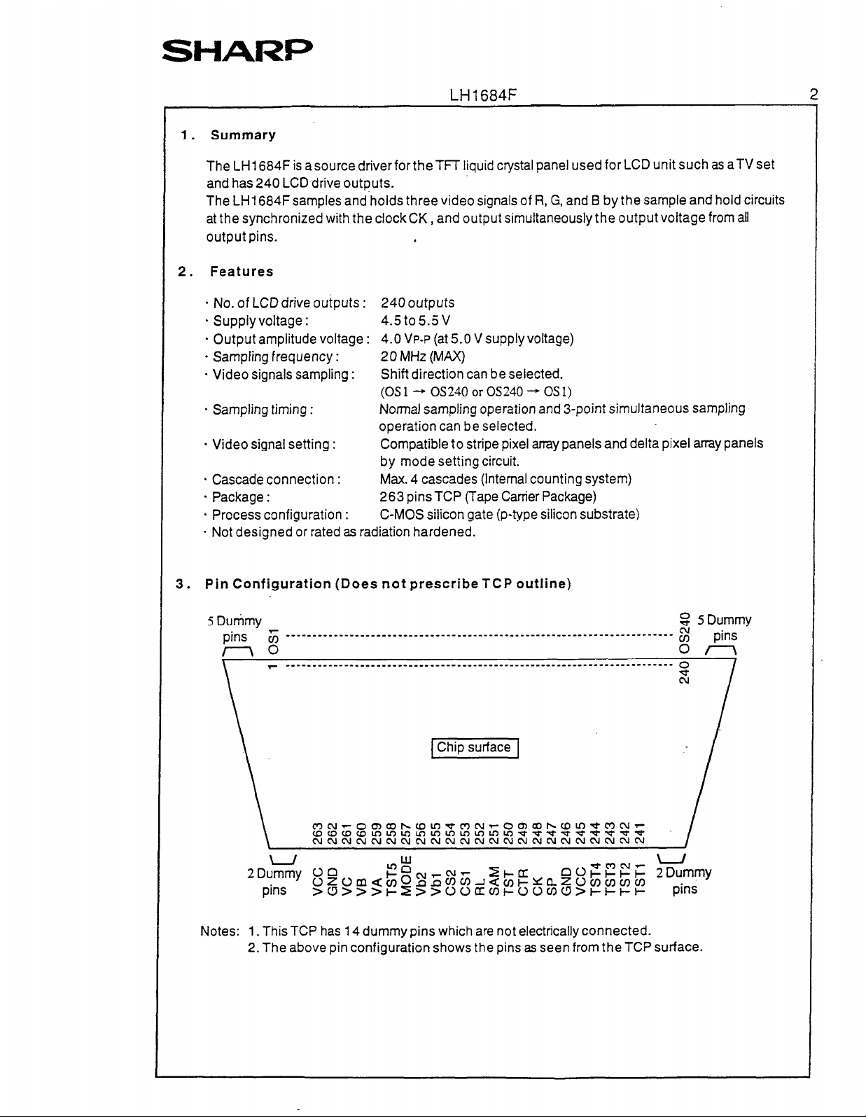
Pin Configuration (Does not prescribeTCP outline)
5 Dummy
Pi0
Notes: 1. This TCP has 14 dummy pins which are not electrically connected.
_-.-----__----__--_-____________________---------------------------------
;5
2. The above pin configuration shows the pins as seen from the TCP surface.
$j? 5Dummy
pins
s:
On

SHARP
LH 1684F 3
4. Block Diagram
RL
CSl
cs2
TST
TSTl
TST2
TST3
1
Numerals in circles indicate the pin number.
Bkdirectional shift
Control
logic
. . . . . . . . . . . . . . . . . . . . . . . . . . . .
, --_-_-_-____------_--
6
. . . . . . . . . . . . . . . . . . . . . . . . . . OS240
vcc
Block name I Block function
Control logic
Bi-directional shift register ~ Used as transfer circuit of video sampling start signals.
Sampling signal creation circuit Used to create the sampling signals corresponding to each output
Mode setting circuit / Used to set the form of the video signals to be sent to the sample
Sample and hold circuit
Output circuit
GND
I Used to create signals necessary for controlling cascade sequence
’ and for discharge signal and sampling signals creation circuits, etc.
’ It is possible to set the direction of sampling start signals sequence
/ by setting the FVL pin, from OS1 to OS240 or from OS240 to OS1 .
j pin based on the sampling start signals transferred by the bii directional shift register.
1 and hold circuits.
Used to sample the video signals input from the mode setting circuit I
: at the timing of the sampling signals and hold the sampling datas
I until the next sampling operation.
i The circuit comprises an operational amplifier and an output buffer
1 and outputs the voltage corresponding to the data held in the
/ sample and hold circuit.
OS1
i
I
i
I

SHARP
5. Description of Pins
5.1 Designation of pins
LH 1684F
Pin No. I Pinsymbol / I/O
1 to 240 / OS1 to OS240 0 LCD drive output pins
241 j
242 j
1 243 (
244
245,263 ’
246,262 1
247 1 SP
248 ’
249 ~
250 /
251 : SAM ! I
252
253
254 ’
255 ’ Vbl 1 I
256 Vb2 I
257 I
258
259
260 :
261 i
TSTl / I LSI test pin
TST2 / I LSI test pin
TST3 j I LSI test pin
TST4 ~ I LSI test pin
vcc / - Power supply pins
GND i - GNDpins
/ I Horizontal scanning start pulse input pin
CK j I Horizontal shift clock input pin
CTR / I Analog circuit operation selecting pin .
TST j I LSI test pin
Sampling mode selecting pin
RL : I Sampling sequence selecting pin
CSl I I Cascade sequence setting pin 1
cs2 ~ I Cascade sequence setting pin 2 ,
Bias voltage setting pin for output operational amplifiers ’
Bias voltage setting pin for output buffers
MODE 1 I Video signals form setting pin
TST5 j I LSI test pin
VA I Video signal input pin
VB / I Video signal input pin
vc I I Video signal input pin I
Designation
j Remarks
I
I
i
I
I
I
I
I
I
/
/
/
/
! /
I
I
I
1
I

SHARP
’ “‘684F
l-1 I IL- .
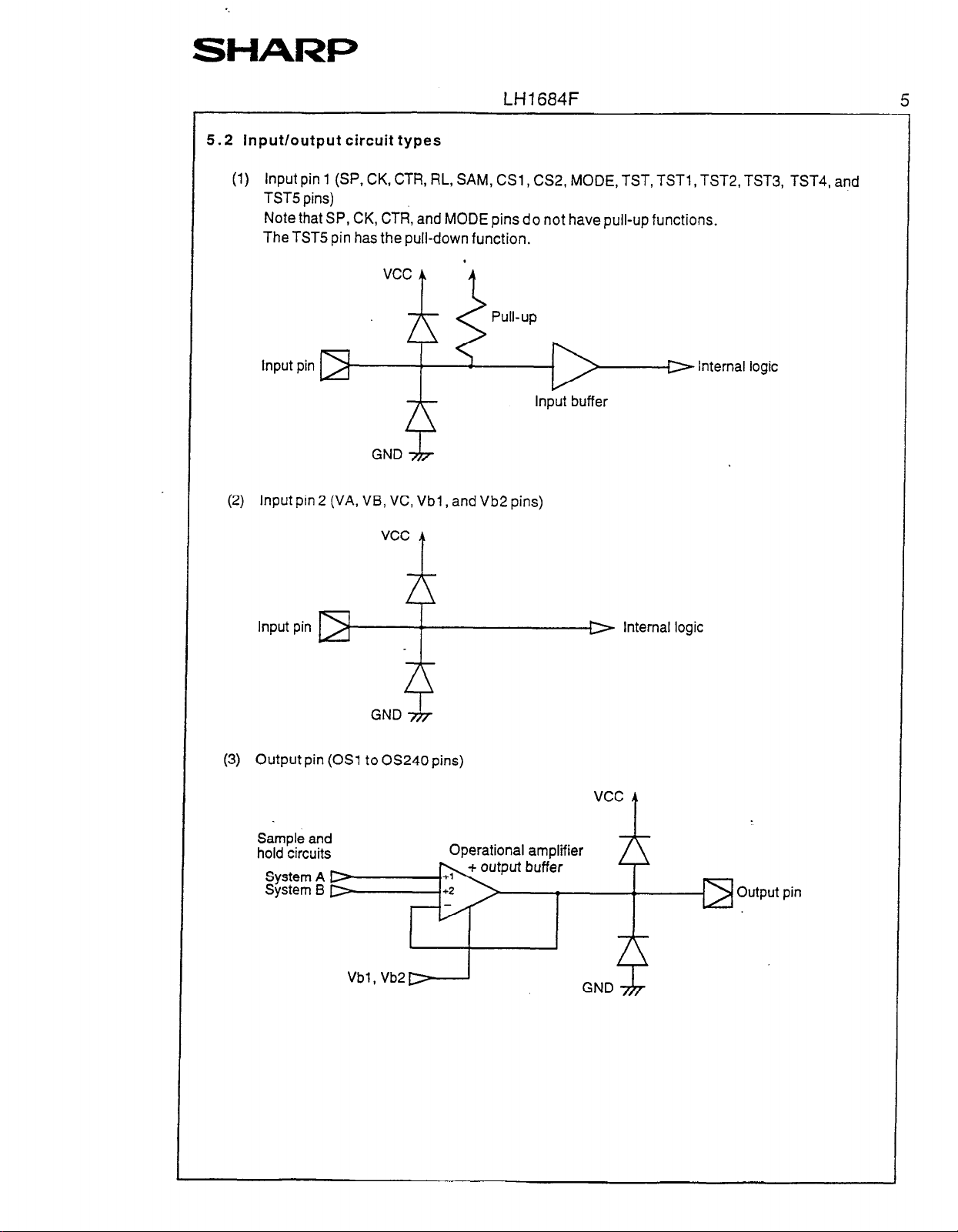
5.2 input/output circuit
(1) Input pin 1 (SP, CK, CTR, RL, SAM, CSl, CS2, MODE, TST, TSTl, TST2, TSTS, TST4, and
TST5 pins)
Note that SP, CK, CTP, and MODE pins do not have pull-up functions.
TheTST.5 pin has the pull-down function.
Input pin
(2) Input pin 2 (VA, VB, VC, Vbl , and Vb2 pins)
types
Input buffer
Internal
logic
Input pin BBp fnternal logic
Output pin (OS1 to OS240 pins)
(3)
vcc
Sample and
hold circuits
Operational
--,:I:-- 7k
ampwer
tput buffer
4
t
Outpu
pin

SHARP
Description of Functions
1 Functions of
Pin symbol
vcc Used as power supply pin, which is normally connected to +5.6 V.
GND / Used as GND pin, which is connected to OV.
TST : Used as pin for LSI testing. Must be connected to VCC.
TSTl to TST4 I Used as pins for LSI testing. Must be connected to VCC.
TST5
SP
CK
CTR i Used as input pin of selecting video signals sampling circuits and selecting input
SAM Used as input pin for setting the selecting of normal sampling operation or S-point
i-
RL
CSl, cs2 1 Used as input pins for setting of chip cascade sequence.
pin
: Used as pin for LSI testing. Must be connected to GND.
j Used as input pin of horizontal scanning start pulse.
j Used as input pin of horizontal shift clock.
/ Video signals are sampled in order at rise timing and fall timinglof CK.
/ signals of output operational amplifiers.
j simultaneous sampling operation.
i For normal sampling operation, video signals are sampled in order 7 LCD drive output.
For 3-point simultaneous sampling operation, video signals are sampled in order
I simultaneously 3 LCD drive outputs.
j For either operation, sampling signals are shifted at every rise timing and fall timing of
j horfzontal shift clock of CK pin (half cfock) , and their sampling perfod is equal to the
period of one clock.
Used as input pin for setting the shift direction of video signals sampling sequence.
~ Video signals are sampled in the order of from OS1 to OS240 when set to “H” and in tht
order of from OS.240 to OS1 when set to “L”.
/ Set chip cascade sequence as shown in the table below.
and
Operations
Pin functions
’ Cascadesequence ’ cs1 cs2
I
I
; For details, refer to “6-2. Operation of function” on page 7.
MODE ’ Used as input pin for setting form of video signals for sampling.
/ By mode setting circuit, video signals are sampled and output with respect to OS1 to
i OS246 in the order of VB, VA, and VC when set to “H” and in the order of VC, VB, and
VA when set to ‘IL”.
/ For details, refer to “6-2. Operation of function” on page 7.
1 Do not use this function in “OPEN” condition.
Vbl r Used as pin for setting the bias voltage of operational amplifiers in output circuits.
Vb2
VA, VB, VC Used as input pins of video signals.
OS1 to OS240 j Used as LCD drive output pins.
i Used as pin for setting bias voltage of buffers in output circuits.
/ VB, VA, VC, ._. VB. VA, VC or VC, VB, VA. . . .
; drive outputs OSl, OS2,OS3. . . . 08238,05239,OS240 by MODE pin setting
1 condition.
i All output pins discharge simultaneously at the timing of internal
; after discharge is completed, they output voltage corresponding to sampled video
: signals.
1st H I H
I
2nd
3rd
4th / L j L
L ! H
I
H ; L
VC, VB, VA are input with respect to LCD
discharge signal and

-.
SHARP
6.2 Operation of function
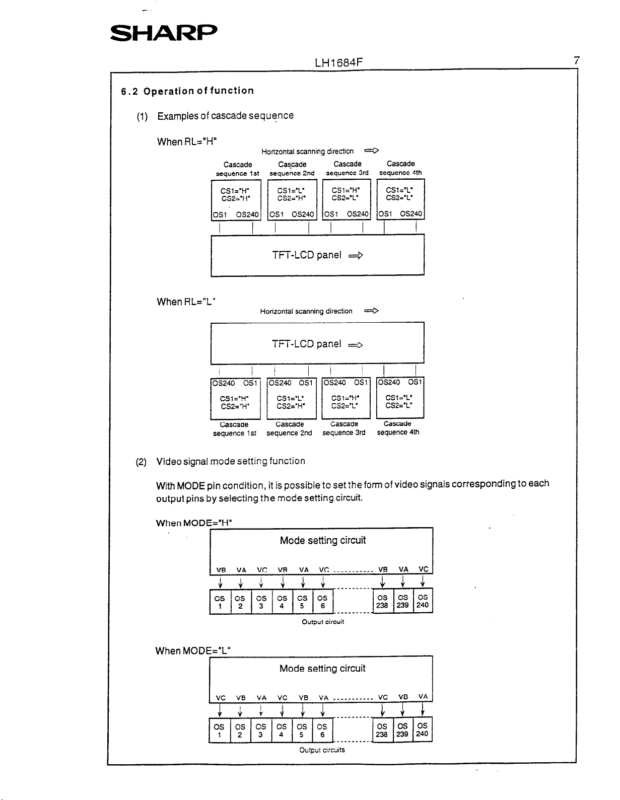
(1) Examples
of cascade
When RL=“H”
Cascade Cascade Cascade Cascade
When RL=“L”
LH1684F
sequence
Horizontal scanning direction e
I
I
TFT-LCD panel c‘,
Horizontal scanning direction
TFT-LCD panel =>
7
e
CSl=‘H’
CSP=‘H’ CSP=‘H’
I
--I
Cascade
sequence 1st sequence2nd sequence 3rd
CSl=‘L
II
Cascade
II
CSl=‘H’
CSL=‘L
Cascade
Cascade
sequence 4th
(2) Video signal mode setting function
With MODE pin condition, it is possible to set the fon of video signals corresponding to each
output pins by selecting the mode setting circuit.
When
MODE=“H”
j..
I I I I
OS OS OS OS OS OS
1 2 3 4 5
6
Output circuit
When MODE=‘L”
Mode setting circuit
Output ciicuits

LH 1684F
(3)
Output circuit type
The LH1684F samples video signals by the sample and hold circuits of 2 systems and outputs
the voltage corresponding to the sampled data by the input switching operational amplifiers.
Sample and hold circuits and output circuits are as shown in the diagram below.
When CTR=“H”, the LH1684F samples the data to system A of the sample and hold circuits
and outputs the voltage corresponding to the voltage sampled by capacitor B of system B.
When CTR=“L”, the LH1684F samples the data to system B of the sample and hold circuits
and outputs the voltage corresponding to the voltage sampled by capacitor A of system A.
System A of sample and hold circuits
r---------------------------------.
L_____________---__________________
System B of sampie and hold circuits
.1
8
Therefore, it
is necessary to repeat sampling operation
and output operation by exchanging
CTR signal to “H” and “L” for every SP signal, usually.
When CTFI signal is set to “H” or “L” several times for SP signal, the same voltage is output
continuously during such period.
The output voltage corresponds to the data sampled by the previous sampling operation.
Timing of operation is as follows.
SP
CTR
I
4 4
System
A
System B output 0 Sampling
Sampling 1 output 1
--A
Sampling
2 output 2 output 2 Sampling 4
3 Sampling 3’ output 3’

SHARP
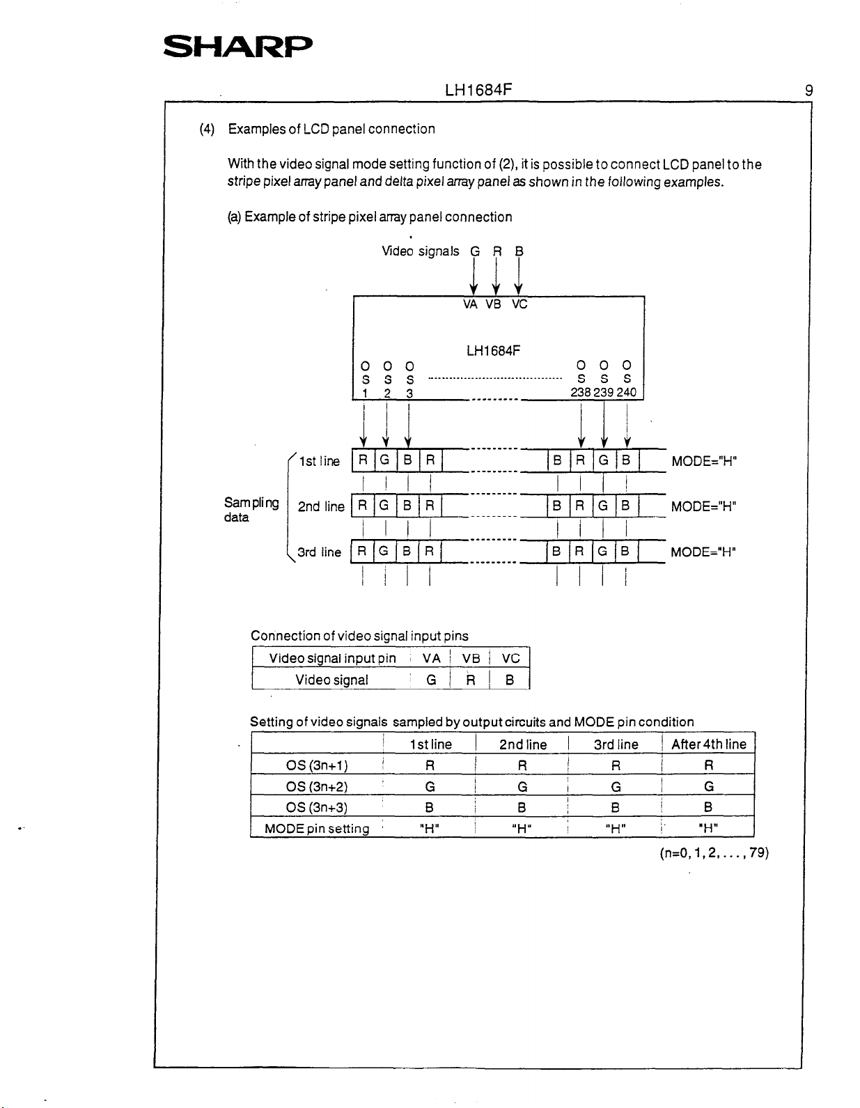
(4) Examples of LCD panel connection
With the video signal mode setting function of (2) it is possible to connect LCD panel to the
stripe pixel array panel and delta pixel array panel as shown in the following examples.
(a) Example of stripe pixel array panel connection
‘1st line
LH1684F
Video signals p 7 f
Sampling
data
Connection of video signal input pins
Setting of video signals sampled by output circuits and MODE pin condition
2nd line R G B R
3rd line R G B R
Videosignal input pin ; VA / VB 1 VC
Video signal ‘G/RIB
OS(3n+l) j R / R j R ; R
OS (3n+2) G
OS (3n+3) B i
MODE pin setting
m::;:-;;:: MODE=“H”
I 1 I I
~:]::-:::: IB IR IG /B 1
I I I I
1
lstline I 2nd line 1 3rd line
I
U,,” 1
1 ; 1 d 1; 1 Ii /
I i I
i
I I I I
G
B B j
“,,” ;
I
I G
/
“H” ! “H”
MODE=“H”
/ After 4th line
/
I
;.
(n=O, 1,2,. . . ,79)
G
B
 Loading...