

Page 1
q
SERVICE MANUAL
■ LEAD-FREE SOLDER
CODE : 00Z
LD26SH3U/E
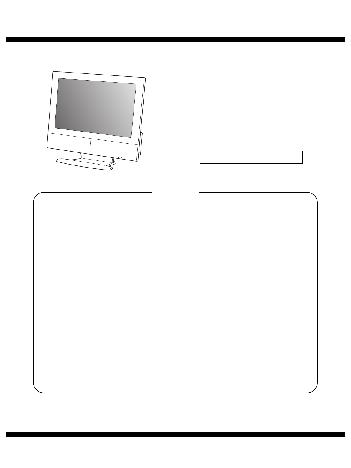
LCD COLOR TV
MODEL
LEAD-FREE SOLDER MODEL
CONTENTS
LD-26SH3U
LEAD-FREE SOLDER MODEL
CHAPTER 1. OUTLINE OF THE PRODUCT,
NOMENCLATURE AND FUNCTION. . . . . . . . . . . . . . . . . .1 - 1
CHAPTER 2. CONNECTION, ADJUSTMENT, OPERATION,
AND FUNCTIONS . . . . . . . . . . . . . . . . . . . . . . . . . . . . . . . .2 - 1
CHAPTER 3. DISASSEMBLY AND ASSEMBLY . . . . . . . . . . . . . . . . . . . .3 - 1
CHAPTER 4. TROUBLE SHOOTING . . . . . . . . . . . . . . . . . . . . . . . . . . . .4 - 1
CHAPTER 5. BLOCK DIAGRAM . . . . . . . . . . . . . . . . . . . . . . . . . . . . . . . .5 - 1
CHAPTER 6. HARDWARE DESCRIPTION. . . . . . . . . . . . . . . . . . . . . . . .6 - 1
CHAPTER 7. CIRCUIT DIAGRAM & PWB LAYOUT. . . . . . . . . . . . . . . . .7 - 1
Parts marked with "!" are important for maintaining the safety of the set. Be sure to replace these parts with specified
ones for maintaining the safety and performance of the set.
This document has been published to be used
SHARP CORPORATION
for after sales service only.
The contents are subject to change without notice.
Page 2
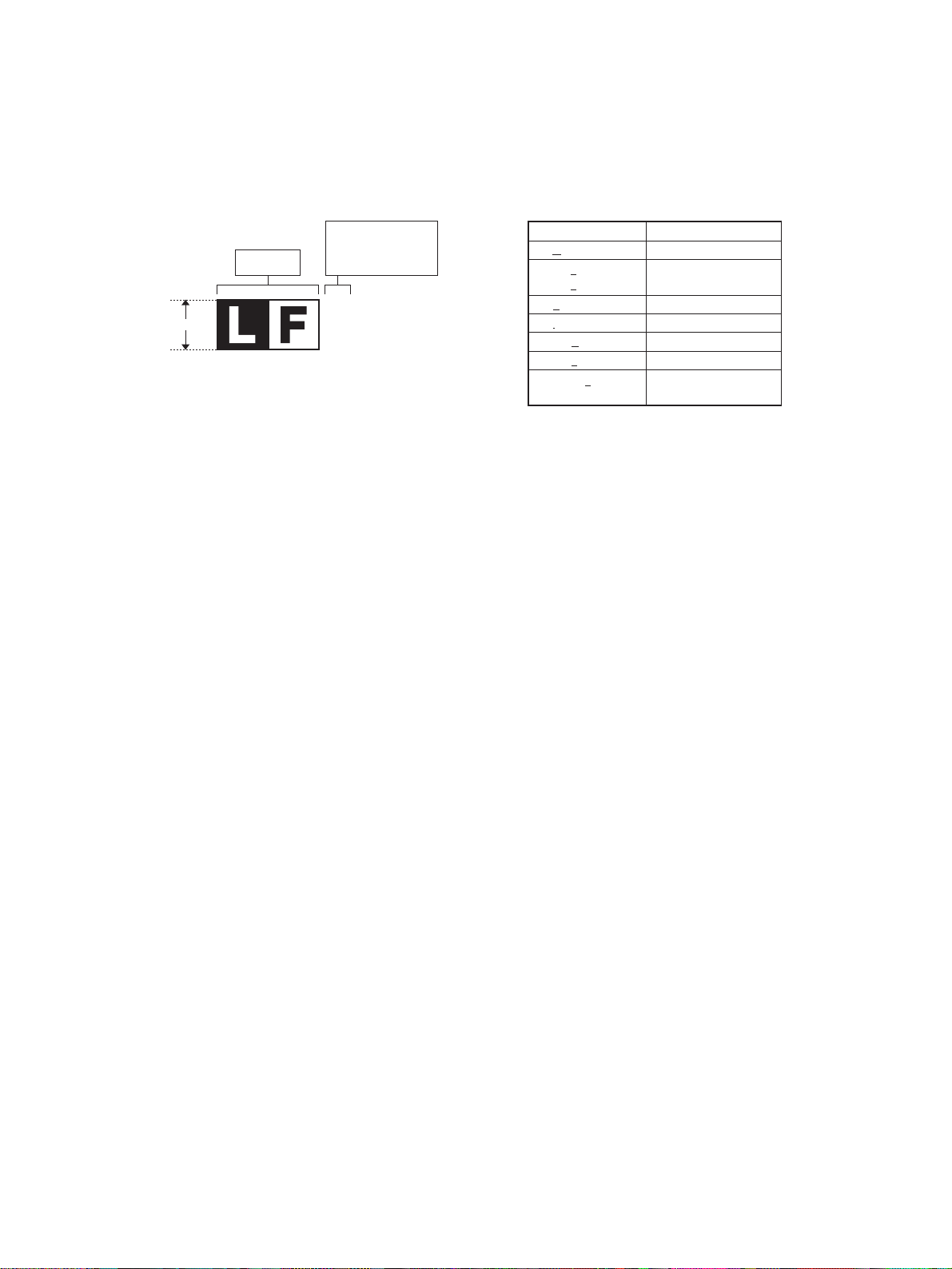
■ LEAD-FREE SOLDER
The PWB’ s of this model employs lead-free solder. The “LF” marks indicated on the PWB’s and the Service Manual mean “Lead-Free” solder. The
alphabet following the LF mark shows the kind of lead-free solder.
Example:
<Solder composition code of lead-free solder>
Solder composition
Sn-Ag-Cu
Sn-Ag-Bi
Sn-Ag-Bi-Cu
Sn-Zn-Bi
Sn-In-Ag-Bi
Sn-Cu-Ni
Sn-Ag-Sb
Bi-Sn-Ag-P
Bi-Sn-Ag
5mm
Lead-Free
Solder composition
code (Refer to the
table at the right.)
a
(1) NOTE FOR THE USE OF LEAD-FREE SOLDER THREAD
When repairing a lead-free solder PWB, use lead-free solder thread. Never use conventional lead solder thread, which may cause a breakdown or an
accident.
Since the melting point of lead-free solder thread is about 40°C higher than that of conventional lead solder thread, the use of the exclusive-use soldering iron is recommendable.
Solder composition code
a
b
z
i
n
s
p
(2) NOTE FOR SOLDERING WORK
Since the melting point of lead-free solder is about 220°C, which is about 40°C higher than that of conventional lead solder, and its soldering capacity
is inferior to conventional one, it is apt to keep the soldering iron in contact with the PWB for longer time. This may cause land separation or may
exceed the heat-resistive temperature of components. Use enough care to separate the soldering iron from the PWB when completion of soldering is
confirmed.
Since lead-free solder includes a greater quantity of tin, the iron tip may corrode easily. Turn ON/OFF the soldering iron power frequently.
If different-kind solder remains on the soldering iron tip, it is melted together with lead-free solder. To avoid this, clean the soldering iron tip after completion of soldering work.
If the soldering iron tip is discolored black during soldering work, clean
and file the tip with steel wool or a fine filer.
LD-26SH3U
Page 3
CHAPTER 1. OUTLINE OF THE PRODUCT, NOMENCLATURE AND FUNCTION
1. SPECIFICATIONS
PRODUCT SPECIFICATIONS
Model name LD-26SH3U
LCD display 26" Advanced Super-V and Anti-Glare
Low-Reflection TFT LCD module
Actual display size 25
Resolution (max.) 1366
Displayable colors
33
/64" (64.8 cm) measured diagonally
768
u
Approx. 16.77 million colors (8 bit)
(max.)
Dot pitch (H
Brightness (max.) 450 cd/m
V) 0.4135 mm u 0.4135 mm
u
2
(The screen brightness deteriorates over time.
Constant brightness cannot be maintained.)
Contrast ratio 800:1
Angle of visibility Left-right 170°; up-down 170°
Screen display size
V)
(H
u
(contrast ratio
564.8 mm
u
(22 ¼"
s
317.6 mm
u
12 33/64")
10)
Video signal Analog: Analog RGB (0.7 Vp-p) [75Ω]
Digital: DVI standard based on 1.0
Sync signal Separate Sync (TTL level: +/-),
Sync on Green,
Composite Sync (TTL level: +/-)
Video signal format NTSC
Expansion
compensation
Digital scaling (Enlarges VGA/SVGA/XGA
etc. to full screen size.)
[Enlarged display (full screen, fixed aspect
ratio)]
- 1:1 display is not possible.
Plug & Play VESA DDC2B compatible
Power management VESA : based on DPMS
DVI : based on DMPM
Speaker output 20 W in total
3
Input terminals Video image : RCA pin
Component image:
S-video image :
u
u
HDMI : u
DVI-D 24 pin
1
u
u
1
2
1
(Also used as a computer digital signal input
terminal)
Audio : RCA pin (L/R
4)
u
Antenna : F-type
Computer signal:
Analog : mini D-sub 15 pin (3 rows)
Digital : DVI-D 24 pin
1
u
(Also used as a DVI image input terminal)
Computer audio: mini stereo jack (3.5mm)
Output terminals Video image: RCA pin
Audio : RCA pin (L/R
1
u
1)
u
Headphone : mini stereo jack (φ 3.5 mm) u
Antenna : F-type
Receivable TV
channels
VHF: 2 through 13; UHF: 14 through 69;
Cable: 1 through 125
Screen tilt Upward approx. 0° - 5°;
downward approx. 0° - 5°
Screen swivel Approx. 30° from left through right
Power supply 100 VAC - 240 VAC, 50/60 Hz
Temperature of
operating environment
Power consumption 118 W; 0.1 W in standby;
Dimensions
D u H)
(W
u
Weight Approx. 18.5 kg; 40.7 lb. (with stand)
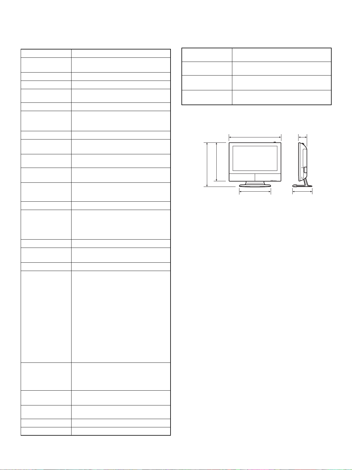
■ Dimensions (Units: mm (inch))
)
16
)
/
64
11
1
500 (19
559 (22 /
• Power cord: approx. 1.8 m (5' 10")
• PC analog signal cable: approx. 1.8 m (5' 10")
• PC audio cable: approx. 1.8 m (5' 10")
• Digital signal cable, NL-C04J (purchased separately):
approx. 2.0 m (6' 6")
Note: As a part of our policy of continuous improvement, SHARP
reserves the right to make design and specification changes for
product improvement without prior notice. The performance
specification figures indicated are nominal values of production
units. There may be some deviations from these values in individual units.
1
u
1
u
1
5°C - 35°C (41°F - 95°F)
1.0 W in power-saving mode
Approx. 667 mm
(Approx. 26
280 mm u 559 mm
u
17
/64" u 11 1/32" u 22 1/64")
Approx. 15.6 kg; 34.4 lb. (without stand)
667 (26
398(15
1
/64
43
/64
)
)
110 (41 /32)
280 (11
/32
1
1
)
LD-26SH3U OUTLINE OF THE PRODUCT, NOMENCLATURE AND FUNCTION
1 – 1
Page 4
■ Relevant signal timings (PC mode)
Screen resolution Hsync Vsyn
VESA 640
Wide 1280u720 44.7kHz 60Hz 74.4MHz
US text 720u400 31.5kHz 70Hz 28.3MHz
Power
Macintosh
series
: Available
o
• Recommended resolution is 1360
• All are compliant only with non-interlaced.
• Depending on the type of computer to be connected, the display may
not work correctly even when the above relevant signals are input.
• Frequencies for Power Macintosh are reference values. To connect,
another adapter (commercially available) may be required.
• For digital connection, the TV can be connected to a computer with a
DVI-compatible output terminal (DVI-D 24 pin or DVI-I 29 pin).
(Depending on the type of computer to be connected, the display may
not work correctly.)
• If the TV is receiving timing signals that are not compatible, "Out of
Timing" will appear. Follow your computer's operation manual to set
the timing so that it is compatible with the TV.
• If the TV is not receiving any signal (sync signal), "No Signal" will
appear.
480 31.5kHz 60Hz 25.175MHz
u
37.9kHz 72Hz 31.5MHz
37.5kHz 75Hz 31.5MHz
800u600 35.1kHz 56Hz 36.0MHz
37.9kHz 60Hz 40.0MHz
48.1kHz 72Hz 50.0MHz
46.9kHz 75Hz 49.5MHz
848u480 31.0kHz 60Hz 33.75MHz
1024u768 48.4kHz 60Hz 65.0MHz
56.5kHz 70Hz 75.0MHz
60.0kHz 75Hz 78.75MHz
1280u768 47.8kHz 60Hz 79.5MHz
60.3kHz 75Hz 102.25MHz
1360u768 47.7kHz 60Hz 85.5MHz
480 35.0kHz 66.7Hz 30.2MHz
u
640
832u624 49.7kHz 74.6Hz 57.3MHz
1024u768 60.2kHz 75Hz 80.0MHz
768, 1280 u 768, or 1024 u 768.
u
Dot
frequency
Ana-
log
oo
oo
oo
o -
oo
oo
oo
oo
oo
oo
oo
oo
oo
oo
oo
oo
o -
o -
o -
Digi-
tal
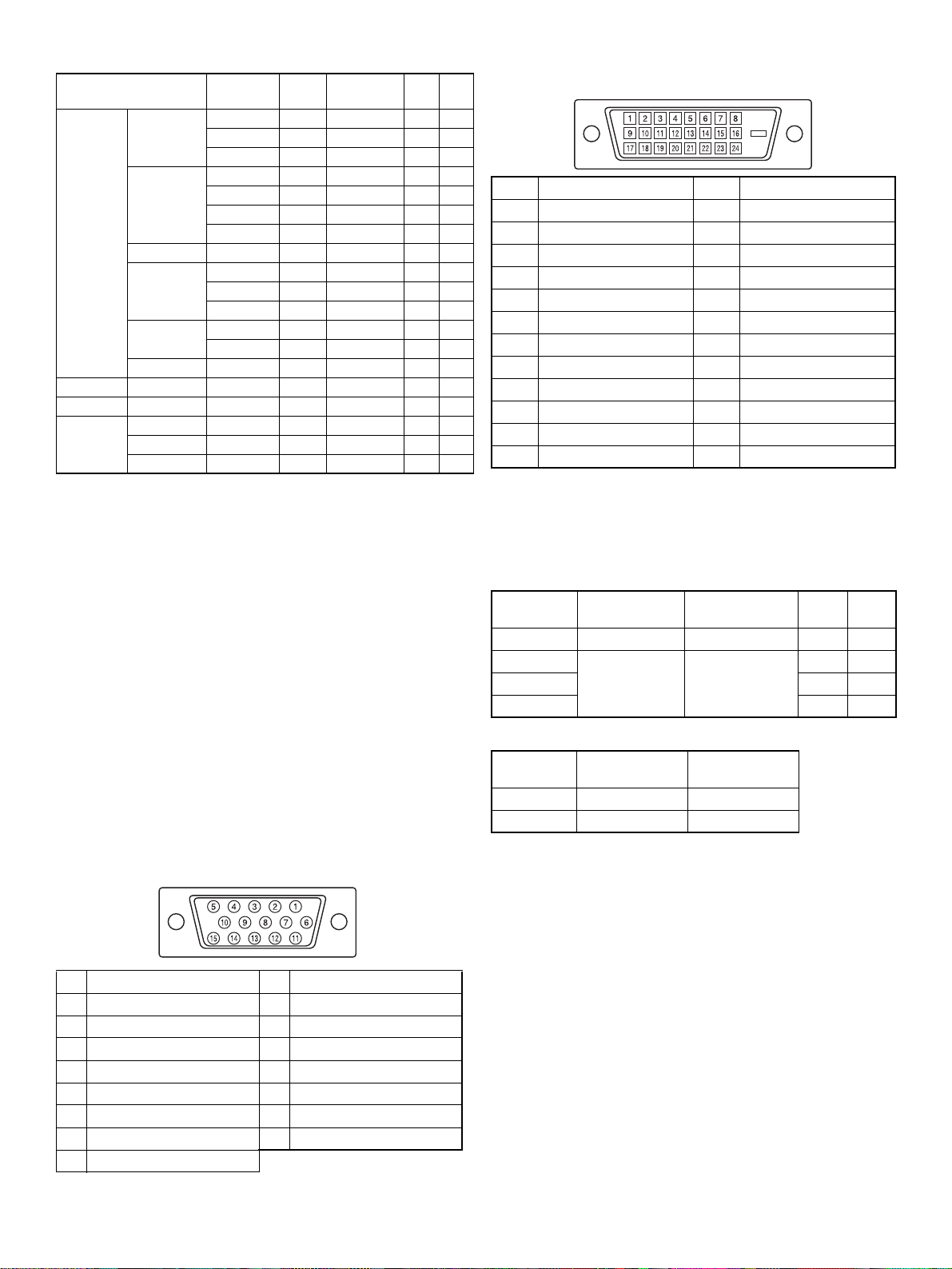
■ The DVI-D input connector pin
(DVI-D connector with 24 pins)
No. Function No. Function
1 TMDS data 2
2 TMDS data 2+ 14 +5V
3 TMDS data 2/4 shield 15 GND
4 N.C. 16 Hot plug detection
5 N.C. 17 TMDS data 0
6 DDC clock 18 TMDS data 0+
7 DDC data 19 TMDS data 0/5 shield
8N.C. 20N.C.
9 TMDS data 1
10 TMDS data 1+ 22 TMDS clock shield
11 TMDS data 1/3 shield 23 TMDS clock +
12 N.C. 24 TMDS clock
-
-
13 N.C.
-
21 N.C.
-
■ Power management
The monitor is based on the VESA DPMS and the DVI DMPM standards. To activate the power management function, the video card and
the computer used with it must also conform to these standard.
• DPMS: Display Power Management Signaling
DPMS mode Screen
ON Display on 118 W Yes Yes
STANDBY
SUSPEND Yes No
OFF No No
• DMPM: Digital Monitor Power Management
DMPM mode Screen
ON Display on 118 W
OFF Display off 1.0 W
Display off 1.0 W
Power
consumption
Power
consumption
H-sync V-sync
No Yes
■ The analog RGB input connector pin
(Mini D-sub connector with 15 pins)
No. Function No. Function
1 Red video signal input 9 +5V
2 Green video signal input 10 GND
3 Blue video signal input 11 N.C.
4 N.C. 12 DDC data
5 GND 13 For Hsync signal input
6 For red video signal GND 14 For Vsync signal input
7 For green video signal GND 15 DDC clock
8 For blue video signal GND
LD-26SH3U OUTLINE OF THE PRODUCT, NOMENCLATURE AND FUNCTION
■ DDC (Plug & Play)
This monitor supports the VESA DDC (Display Data Channel) standard.
DDC is a signal standard for carrying out Plug & Play functions on the
monitor or computer. It transfers information such as degree of resolution between the monitor and computer. You can use this function if
your computer is DDC compliant and if it is set so that it can detect the
Plug & Play monitor.
There are many varieties of DDC due to the differences between systems. This monitor works with DDC2B.
1 – 2
Page 5
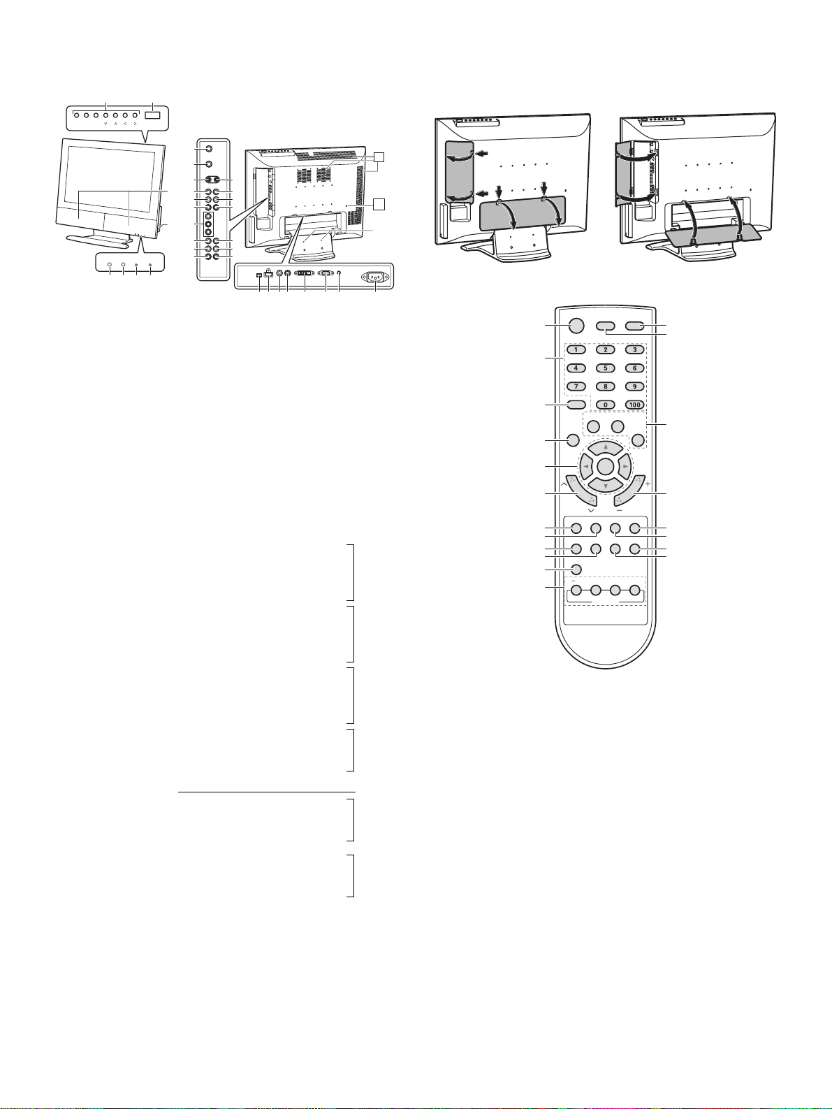
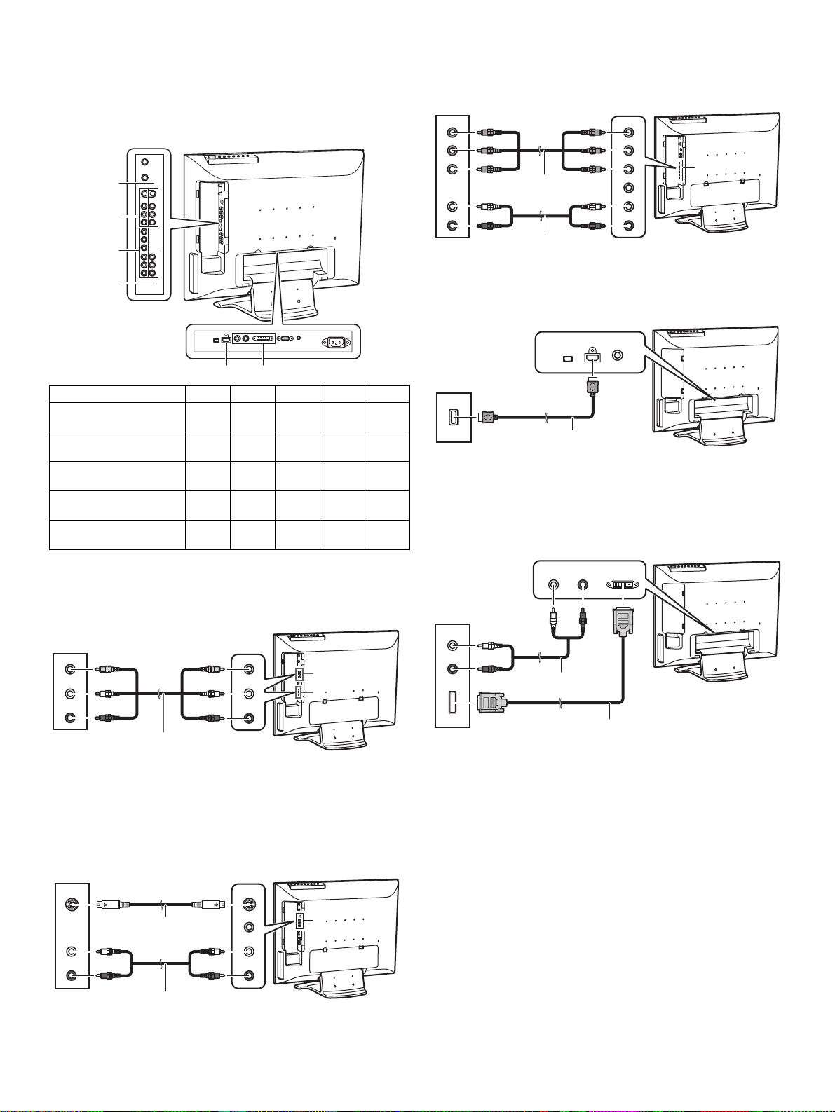
2. PRODUCT DESCRIPTION
■ Main unit ■ Removing/replacing the terminal cover
12
POWERVOL
CH
ENTERMENUINPUT
Removing the cover Replacing the cover
9
F
G
3
H
I
J
4
K
L
M
OPC POWER
56
Control buttons
1
POWER button
2
Speakers
3
Headphone terminal
4
Remote control sensor
5
OPC (Optical Picture Control) sensor
6
OPC LED
7
N
87
O
P
Q
R
S
T
U
Y
VW X
Z[\
Green : OPC is on.
Off : OPC is off.
POWER LED
8
Green : in use
Red : in standby mode
Orange : in power-saving mode (only for PC mode)
Off : power off
Antenna input terminal
9
Antenna output terminal
F
S-video input terminal
G
Video input terminal
H
Audio input terminal - Left
I
Audio input terminal - Right
J
Component input terminals
K
Video input terminal
L
Audio input terminal - Left
M
Audio input terminal - Right
N
S-video input terminal
O
Video input terminal
P
Audio input terminal - Left
Q
Audio input terminal - Right
R
Video output terminal
S
Audio output terminal - Left AV-OUT
T
Audio output terminal - Right
U
Optional terminal (For factory use only)
V
HDMI input terminal AV-IN 4
W
Audio input terminal - Left
X
Audio input terminal - Right AV-IN 5
Y
DVI input terminal
Z
(DVI-D 24 pin)
(Also available as a digital RGB input terminal for PC mode)
PC analog RGB input terminal (Mini D-sub 15 pin) PC-IN
[
PC audio input terminal
\
Power input terminal
]
Lug-hole for cable clamp
^
A Ventilation openings
Never block these openings as this may lead to overheating inside
the TV and result in malfunction.
B Security lock anchor
By connecting a security lock (commercially available) to the security lock anchor, the TV is fixed so that it cannot be transported.
The security slot works in conjunction with Kensington Micro Saver
Security Systems.
A
B
^
]
AV-IN 1
AV-IN 2
AV-IN 3
■ Remote control
POWER
1
2
3
4
5
6
7
8
9
F
G
H
POWER button
1
Channel buttons
2
FLASHBACK button
3
MENU button
4
5 b c e d
CH (channel) buttons
6
RETURN button
7
EXIT button
8
VIEW MODE button
9
PICT MODE button
F
SLEEP button
G
PIP/SPLIT buttons (ON/OFF, SIZE/MOVE, SWAP, and SELECT)
H
INPUT button
I
DISPLAY button
J
Input buttons (TV, AV, and PC)
K
VOL (volume) buttons
L
MUTE button
M
MTS (Multi ch TV Sound) button
N
FREEZE button
O
CC (Closed Caption) button
P
buttons and [ENTER] button
DISPLAY INPUT
FLASH
BACK
TV AV
MENU PC
ENTER
RETURN
EXIT MTS MUTE
VIEW MODE PICT MODE
SLEEP
ON/OFF SIZE/MOVE
CC FREEZE
SWAP SELECT
PIP/SPLIT
I
J
K
L
VOLCH
M
N
O
P
LD-26SH3U OUTLINE OF THE PRODUCT, NOMENCLATURE AND FUNCTION
1 – 3
Page 6
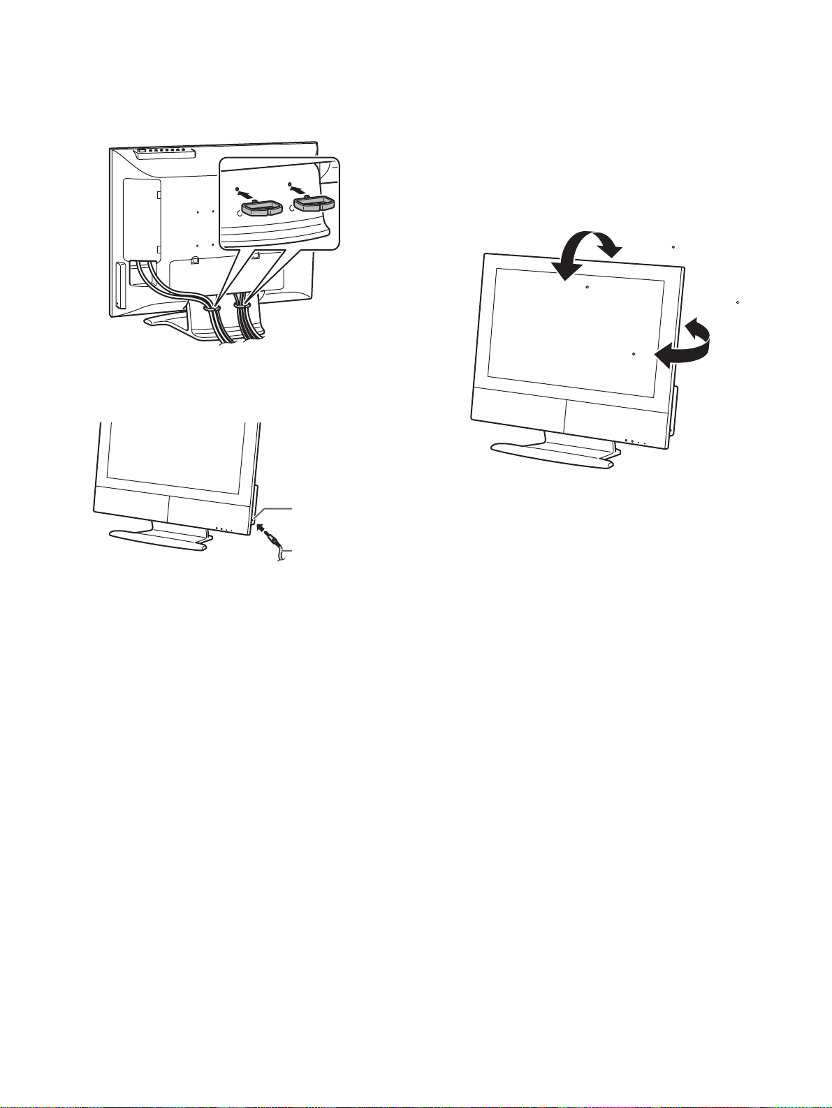
■ Cable clamp
Use the supplied cable clamps to secure the cables connected to the
terminals.
Caution: When adjusting the viewing angle, cables may be pulled.
Therefore, ensure that the cables have sufficient slack.
■ Using headphones (commercially available)
You can connect headphones with a mini stereo jack ( φ 3.5 mm) to the TV
.
■ Angle adjustment
Adjust to an easy to view angle.
Caution: • Be sure to hold both sides of the TV when adjusting the view-
ing angle. The LCD panel used in this TV is made of glass.
Pressure from hands on the LCD panel could cause damage.
• Be careful not to allow your fingers to be pinched.
• Do not put your hand or objects near the stand.
When changing the viewing angle horizontally, the stand
moves and may hit the objects or cause injury to your hand
or fingertips.
approx. 5
approx. 5
approx.15
approx. 15
Headphone
terminal
Headphones
Notes:
• When headphones are connected:
- No sound can be heard from the TV speakers.
- In addition, when "Output Select" is set to "Variable1" or
"Variable2" in the Option menu, no sound via the audio output
terminals can be heard either.
• The Virtual Dolby Surround function cannot be used.
• The Audio menu cannot be adjusted.
LD-26SH3U OUTLINE OF THE PRODUCT, NOMENCLATURE AND FUNCTION
1 – 4
Page 7
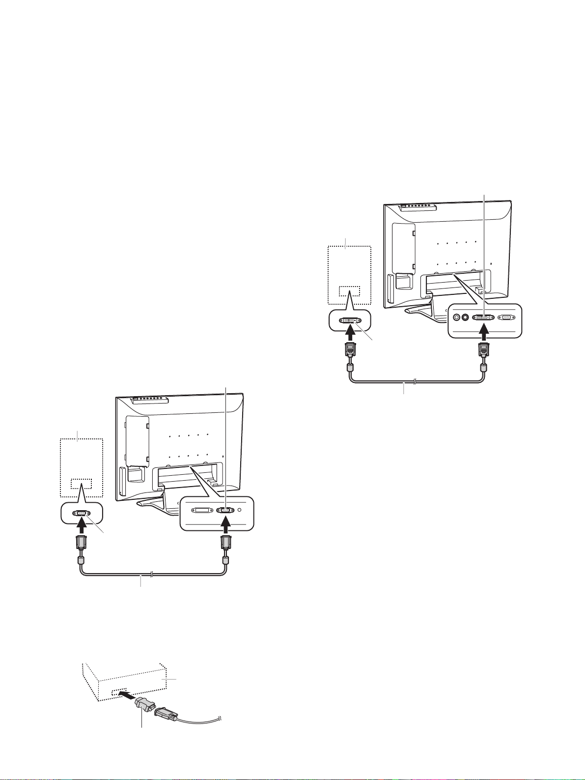
CHAPTER 2. CONNECTION, ADJUSTMENT, OPERATION, AND FUNCTIONS
1. CONNECTING THE MONITOR AND TURNING THE MONITOR ON AND OFF
1-1. Connecting the TV to a computer
Caution:
• When connecting, ensure that the TV and all the equipment you are connecting to it are switched off.
• Be careful not to over bend the cable or add extension
cords as this could lead to a malfunction.
Notes:
• When using the TV with an analog connection, perform an automatic
screen adjustment under the following conditions:
- Using the TV for the first time.
- After having changed the system settings during use.
• When using the TV with a digital connection, automatic screen
adjustment is unnecessary.
• When connecting to a notebook computer and the notebook computer's screen is set so that it is displaying at the same time, the MSDOS screen may not be able to display properly.
In this case, change the settings so that only the TV is displaying.
Installing the set-up information
Depending on the computer or OS, you may have to install the set-up
information for the TV. Refer to "readmee.pdf" (in English) on the
supplied CD-ROM. You need Adobe Reader installed on your computer
to view this PDF file.
■ Analog connection
Connect the supplied PC analog signal cable to the analog RGB output
terminal of the computer.
PC analog RGB input terminal
(Mini D-sub 15 pin, 3 rows)
■ Digital connection
Connect the separately-sold digital signal cable (model name: NLC04J) to the digital RGB output terminal of the computer.
• The TV has an input terminal for connecting to a computer with a
DVI-compatible output terminal (DVI-D 24 pin or DVI-I 29 pin).
(Depending on the type of computer to be connected, the display may
not work correctly.)
DVI input terminal
(DVI-D 24 pin)
Computer
Digital RGB output terminal
(DVI-D 24 pin or DVI-I 29 pin)
Computer
Analog RGB
output terminal
(Mini D-sub 15 pin, 3 rows)
PC analog signal cable (supplied)
• Paying attention to the connector direction, firmly insert the signal cable
straight into the connector, and then tighten the screws at both ends.
If connecting to a D-sub 15 pin 2 row Apple Power Macintosh, attach a
Macintosh conversion adapter (commercially available) to the analog
signal cable.
Power Macintosh
Digital signal cable (separately-sold)
• Paying attention to the connector direction, firmly insert the signal
cable straight into the connector, and then tighten the screws at both
ends.
Notes:
• The DVI input terminal is used for either AV equipment or a computer.Before using this terminal, you need to set "DVI Select" to "PC"
in the Option menu.The factory setting is "AV". After making the connection, follow the procedure below.(Make sure that the connected
computer is switched off.)
1. Press the POWER button to turn on the TV.
2. Press the MENU button to display the MENU screen.
3. Select the Option menu.
4. Set "DVI Select" to "PC".
5. Press the MENU or EXIT button to exit the screen.
6. Press the INPUT or PC button to select "PC DIGITAL" as the dis-
play mode.
7. Turn on power to the connected computer.
• If the image does not appear properly, turn off power to both the TV
and the connected computer. Again, set "DVI Select" to "PC" following steps 1 through 7 above.
Macintosh conversion adapter
LD-26SH3U CONNECTION, ADJUSTMENT, OPERATION, AND FUNCTIONS
2 – 1
Page 8
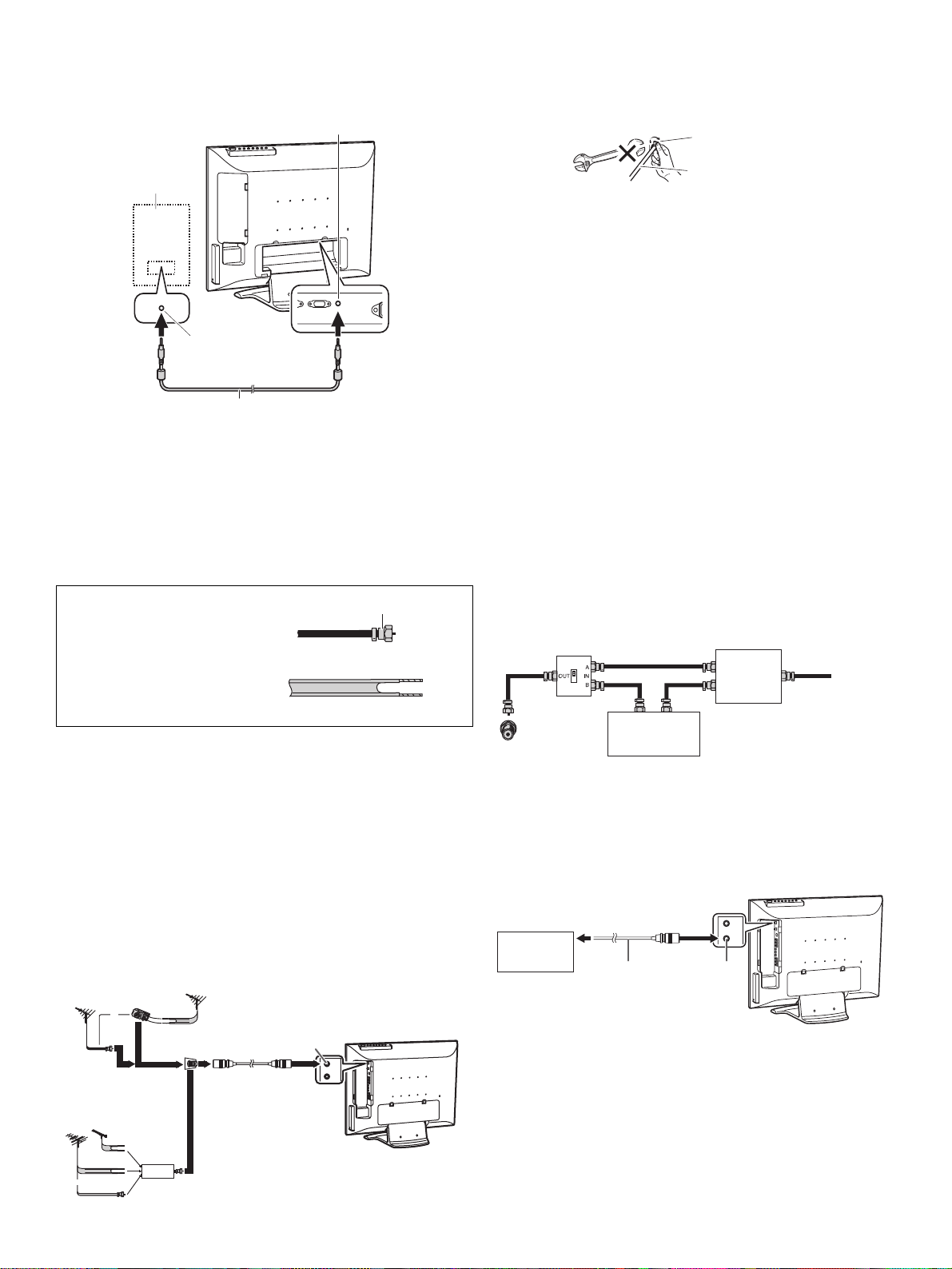
■ Connecting the audio cable
Connect the supplied PC audio cable to the audio output terminal of the
computer.
PC audio input terminal
Caution: When connecting the coaxial cable to the TV, do not tighten F-
type connector with tools. If tools are used, it may cause damage to your TV. (The breaking of internal circuit, etc.)
breaking of internal circuit, etc.)
F-type connector
Computer
Audio output
terminal
PC audio cable (supplied)
1-2. Connecting the TV to a home antenna terminal
Caution: When connecting, ensure that the TV is switched off.
The antenna requirements for good color television reception are more
important than those for black & white television reception. For this reason, a good quality outdoor antenna is strongly recommended.
The following is a brief explanation of the type of connections that are
provided with the various antenna systems.
1. A 75-ohm system is generally
around cable with F-type connector that can easily be attached to a
terminal without tools (commercially available).
A 300-ohm system is a flat "twin-lead"
2.
cable that can be attached to a 75ohm terminal through a 300-75-ohm
adapter (commercially available).
Notes:
• The 75-ohm coaxial cable is recommended.
• When you first receive this TV, it has no memory of any chan-
nels. To receive channels, perform the EZ Setup after the first
power-on, or use "CH Setup" in the Setup menu.
■ Outdoor antenna connection
• Use one of the following two diagrams if you connect an outdoor antenna.
A: Using a VHF/UHF combination outdoor antenna.
B: Using separate VHF and/or UHF outdoor antennas.
• Connect the outdoor antenna cable lead-in to the antenna input
terminal (ANT-IN) on the right side of the TV.
A. Combination VHF/UHF Antenna
VHF/UHF
antenna
coaxial cable
B.Separate VHF and/or
VHF
antenna
300/75-ohm
adapter
(commercially available)
or
75-ohm
UHF Antennas
UHF
antenna
300-ohm
twin-lead
300-ohm
twin-lead
75-ohm
or
coaxial cable
(commercially
Home Antenna
terminal (75-ohm)
Combiner
available)
OUTIN
300-ohm
twin-lead
VHF/UHF
antenna
Antenna input terminal (ANT-IN)
Antenna cable
(commercially available)
F-type connector
75-ohm coaxial cable (round)
300-ohm twin-lead cable (flat)
75-ohm coaxial cable
■ Cable TV (CATV) connection
• A 75-ohm coaxial cable connector is built into the set for easy hookup.
When connecting the 75-ohm coaxial cable to the set, screw the
75-ohm cable to the antenna input terminal (ANT-IN).
• Some cable TV companies offer "premium pay channels".
Since the signals of these premium pay channels are scrambled, a
cable TV converter/descrambler is generally provided to the
subscriber by the cable TV company. This converter/descrambler is
necessary for normal viewing of the scrambled channels.
(Set your TV to channel 3 or 4, typically one of these channels is
used. If this is unknown, consult your cable TV company.)
For more specific instructions on installing cable TV, consult your
cable TV company. One possible method of utilizing the converter/
descrambler provided by your cable TV company is explained below.
Note: An RF switch provided with two inputs (A and B) is required
(commercially available).
"A" position on the RF switch (commercially available):
You can view all unscrambled channels by using the TV's channel
buttons.
"B" position on the RF switch (commercially available):
You can view the scrambled channels via the converter/descrambler by using the converter's channel keys.
RF switch (commercially available)
OUT
Cable TV converter/
descrambler
Antenna input terminal
(ANT-IN)
(commercially
available)
Note: Consult your SHARP Dealer or Service Center for the type of
splitter, RF switch, or combiner that might be required.
■
Connection to an antenna input terminal of AV equipment
A different type of antenna cable is required depending on the shape of
the antenna input terminal of the AV equipment to be connected.
Antenna input
terminal of AV
equipment
Antenna cable
(commercially
available)
Antenna output
terminal
(ANT-OUT)
Note: The signal from the antenna output terminal is less powerful than
when it first enters the TV. Please use a booster (commercially
available), if necessary.
IN
Two-set
signal
splitter
(commercially
available)
Cable TV Line
LD-26SH3U CONNECTION, ADJUSTMENT, OPERATION, AND FUNCTIONS
2 – 2
Page 9
1-3. Connecting the TV to AV equipment
-IN 1 or A
-IN 3
Caution: Ensure that the TV and all the equipment you are connecting
to it are switched off before you begin.
■ Examples of equipment you can connect
Right side of the TV
AV-IN 3
AV-IN 1
AV-IN 2
AV-OUT
AV-IN 4 AV-IN 5
AV-IN 1 AV-IN 2 AV-IN 3 AV-IN 4 AV-IN 5
AV equipment with
video output terminals
AV equipment with
S-video output terminals
AV equipment with
component output terminals
AV equipment with
HDMI output terminals
AV equipment with
DVI output terminals
: Available
o
Note: For information on the connection using the AV-OUT terminals.
ooo--
o - o --
- o ---
---o -
----o
■ AV equipment with component output terminals
Output terminals of
AV equipment
(Green) (Green)
Y
(Blue) (Blue)
Pb
(Red) (Red)
Pr
AUDIO-L
AUDIO-R
Component video cable
(commercially available)
(White) (White)
(Red) (Red)
RCA pin cable (commercially available)
Y
Pb
Pr
VIDEO
AUDIO-L
AUDIO-R
Note: When using the component input terminals, do not connect the
cable to the video input terminal of AV-IN 2.
Right side of the TV
AV-IN 2
■ AV equipment with HDMI output terminals
Rear of the TV
OPTIONHDMIAUDIO-L
Output terminals of
AV equipment
HDMI
HDMI cable (commercially available)
Notes:
• To display an image via the HDMI input terminal, be sure to
select "AV4" as the display mode.
• If necessary, you can make adjustments for HDMI setup using
the Option menu in AV4 mode.
■ AV equipment with DVI output terminals
Rear of the TV
AUDIO-L AUDIO-R DIGITAL
■ AV equipment with video output terminals
Output terminals of
AV equipment
VIDEO
(Yellow)
AUDIO-L
AUDIO-R
Notes:
(White)
(Red)
RCA pin cable (commercially available)
• When using the video input terminal of AV-IN 1 or AV-IN 3, do not
(Yellow)
(White)
(Red)
VIDEO
AUDIO-L
AUDIO-R
connect the cable to the S-video input terminal of the same group.
• When using the video input terminal of AV-IN 2, do not connect the cable to the component input terminals of AV-IN 2.
Right side of the TV
AV-IN 1 or AV-IN 3
AV-IN 2
■ AV equipment with S-video output terminals
Output terminals of
AV equipment
S-VIDEO
S-video cable (commercially available)
AUDIO-L
AUDIO-R
(White)
(Red)
RCA pin cable (commercially available)
(White)
(Red)
S-VIDEO
VIDEO
AUDIO-L
AUDIO-R
Note: When using the S-video input terminal of AV-IN 1 or AV-IN 3, do
not connect the cable to the video input terminal of the same
group.
Right side of the TV
AVAV-IN 1 or A
AV-IN 1 or AV-IN 3
V-IN 3
Output terminals of
AV equipment
AUDIO-L
AUDIO-R
DVI OUT
(White)
(Red)
(White) (Red)
RCA pin cable
(commercially available)
Digital signal cable
(separately-sold, NL-C04J)
Notes:
The DVI input terminal is used for either AV equipment or a computer.
•
Before using this terminal, you need to set "DVI Select" to "AV" or
"PC" in the Option menu. Since the factory setting is "AV", you can use
the DVI input terminal for AV equipment without changing any setting.
To display an image, be sure to select "AV5" as the display mode.
• Once you have set "DVI Select" to "PC" in the Option menu, be sure
to set "DVI Select" back to "AV" before using the DVI input terminal
for AV equipment.After making the connection, follow the procedure
below. (Make sure that the connected equipment is switched off.)
1. Press the POWER button to turn on the TV.
2. Press the MENU button to display the MENU screen.
3. Select the Option menu.
4. Set "DVI Select" to "AV".
5. Press the MENU or EXIT button to exit the screen.
6.
Press the INPUT or AV button to select "AV5" as the display mode.
7. Turn on power to the connected equipment.
• If the image does not appear properly, turn off power to both the TV
and the connected AV equipment.
Again, set "DVI Select" to "AV" following steps 1 through 7 above.
LD-26SH3U CONNECTION, ADJUSTMENT, OPERATION, AND FUNCTIONS
2 – 3
Page 10
1-4. Other features
■ Outputting images and sound to AV equipment
Caution: Ensure that the TV and all the equipment you are connecting
to it are switched off before you begin.
Input terminals of
AV equipment
VIDEO
AUDIO-L
AUDIO-R
(Yellow)
(White)
(Red)
(commercially available)
RCA pin cable
(Yellow)
(White)
(Red)
VIDEO
AUDIO-L
AUDIO-R
The image displayed on the TV screen and the sound can be output via
the AV-OUT terminals to AV equipment. (In PIP/Split mode, the image
displayed in the active window and the sound can be output.)
Image displayed on the TV screen Output from AV-OUT terminals
TV image
Image input from the video
input terminal
Image input from the S-video
input terminal
Image input from the component
input terminals
Image input from the DVI
input terminal
Image input from the HDMI
input terminal
Computer Image
: Available
o
Only the sound is output.
*
After making the connection, select the item you want to set in "Output
Select" using the Option menu, according to your requirements.
(The factory setting is "Fixed". )
• Fixed : Use when connecting to a VCR for recording, etc.
The volume of the sound via the audio output terminals is
fixed.
• Variable1: Use to enjoy the sound from both the TV speakers and
external speakers while watching the image on the TV.
VOL +/- buttons allow you to adjust the sound volume for
both the TV and external speakers.
• Variable2 : Use to enjoy only the sound from the external speakers
while watching the image on the TV. No sound can be
heard from the TV speakers with this setting.
VOL +/- buttons allow you to adjust the sound volume for
the external speakers.
Right side of the TV
AV-OUT
o
o
o
*
-
-
-
*
-
1-5. Connecting the TV to a power source
Caution:
• When connecting, ensure that the TV is switched off.
• Use only the power cord supplied with the TV.
• Be careful not to over bend the cable or add extension cords as this
could lead to a malfunction.
1. Connect the power cord (supplied) to the power input terminal.
2. Place the power plug into an AC outlet.
Power input terminal
1
Power cord (supplied)
Note: If the TV does not operate, disconnect the power cord from the
AC outlet and reconnect it again. The setup must be completed
in the proper order for the TV to function.
AC outlet
2
LD-26SH3U CONNECTION, ADJUSTMENT, OPERATION, AND FUNCTIONS
2 – 4
Page 11
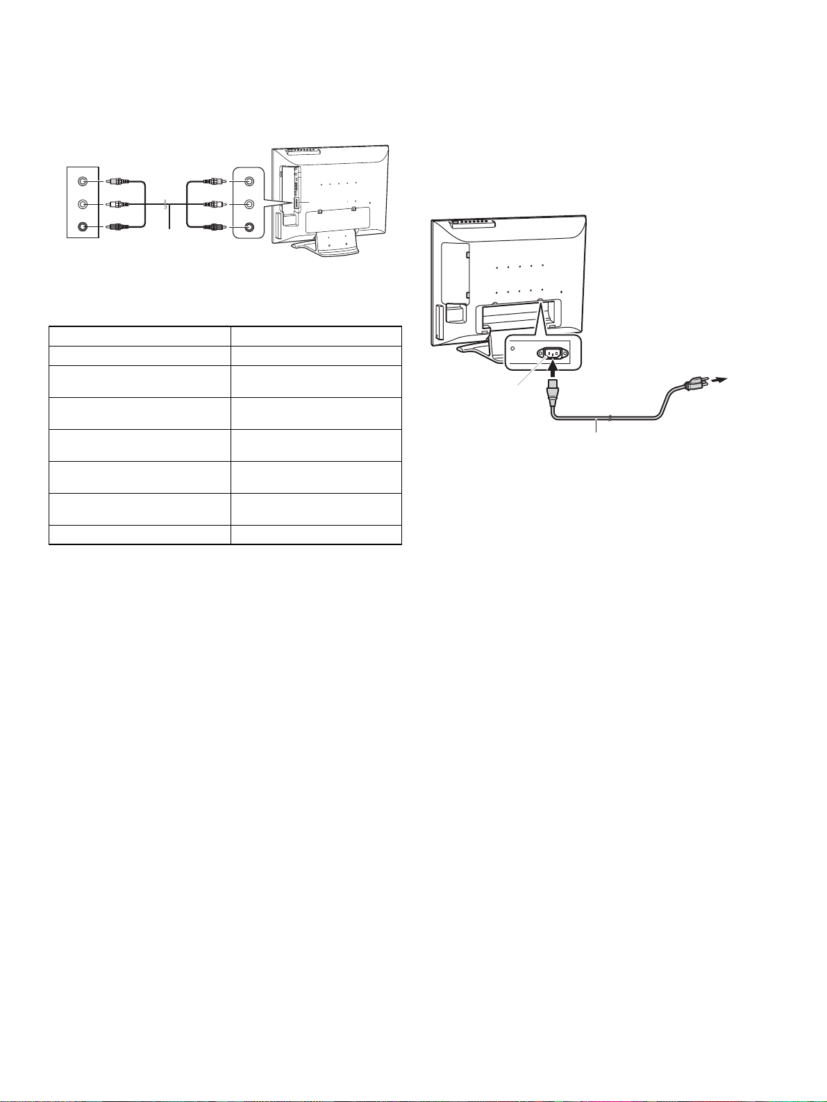
1-6. Setting TV channels (EZ Setup)
When you turn on the TV for the first time, it will automatically memorize
the broadcasting channels where you live.
Make sure you have performed the following steps before you turn on
the TV.
• Insert the batteries into the remote control.
• Connect the antenna cable to the TV.
Make sure what kind of connection (receiving mode) is made with
your TV.
• Plug in the power cord to the TV and AC outlet.
PO WE RVO L
PO W E R
DISPLA Y I NPUT
3. Press [
] buttons to select the desired receiving mode, and
b][c
press [ENTER] button.
Channel search
The tuner will search through all available channels in your area
and save them to the TV memory.
Note:To interrupt the search, press [RETURN] button. It will stop
at the current channel.
EZ Se t u p
Lang uag e
Air/ Cab le
CH Sea rc h
Sea r c h i n g
Air [ 12]
When the search completes, the search screen becomes off and
TV screen becomes minimum channel of TV memory.
Notes:
• You can also select the language using the Setup menu.
• Even if this setup fails to memorize channels in your area, you can
still set the channels using "CH Setup" in the Setup menu.
• EZ Setup will start also after the ALL RESET operation.
FLASH
BA CK
1. Press the POWER button on the TV to turn on the TV.
When the POWER LED lights red, press the POWER button on the
remote control.
Language setting
The language selection screen will be displayed.
EZ Se t u p
2. Press [
Lang uag e
Air/ Cab le
CH Sea rc h
] buttons to select the desired language, and press
b][c
Set th e on-screen d ispla y l anguag e
English
Fr a n çai s
Esp a ñol
[ENTER] button.
Antenna setting
The air/cable selection screen will be displayed.
EZ Se t u p
Lang uag e
Air/ Cab le
CH Sea rc h
Selecting Air/Cab le channel s
Air
Cab l e ( STD)
Cab l e ( HRC)
Cab l e ( IRC)
LD-26SH3U CONNECTION, ADJUSTMENT, OPERATION, AND FUNCTIONS
2 – 5
Page 12
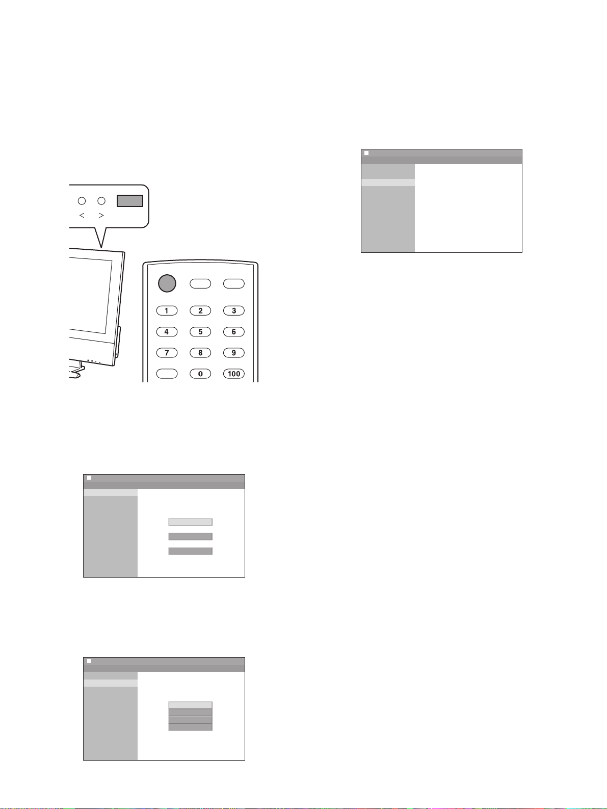
1-7. Instructions for attaching a VESA-compliant mount
An arm or stand based on the VESA standard (commercially available)
can be attached to the TV.
Procurement of the arm or stand is at the customer's discretion.
■ Arms or stands able to be used
Attachments must satisfy the following.
• Compatible with the VESA standard.
• The six screw holes on the section to be attached have a gap of 100
mm between them.
• Not be likely to fall off or break off after being attached to the TV.
■ How to attach the arm or stand
• Be careful not to over bend the cable or add extension cords as this
could lead to a malfunction.
• While following these instructions, please also refer to the installation
instructions in the operation manual included with the arm or stand.
• Because the TV is heavy, we recommend that you perform the operation with two or more persons including yourself.
Caution: • Be careful not to get your fingers pinched between the dis-
play and stand nor to let the stand drop. These could lead
to injury.
• Do not cover or block ventilation openings since insufficient
ventilation can cause overheating.
1. Turn off the TV power using the POWER button on the TV.
2. Remove the terminal covers and the cables.
3. Spread out a soft cloth on a flat surface.
Being careful not to damage the TV, gently lay the TV on it displayside down.
4. Remove the two screws and then remove the rear cover of the
stand.
Notes: • If the stand is hard to remove, pull it toward you while holding it
up slightly.
• The stand is specially made for use with this TV. Once having
removed the stand, never attempt to attach it to another equipment.
• Once having removed the screws, store them together with the
stand.If the stand is ever re-attached, be sure to use the original screws.
Using different screws could lead to a malfunction.
6. Attach the arm to the TV with the six screws.
Note: The screws used to attach the arm should be M4 screws with a
length of 10 mm protruding from the surface to be attached.
Using different screws could cause the TV to fall off or to be
internally damaged.
10 mm
Screw used to attach arm
Soft cloth
5. Remove the four screws and then remove the stand from the TV.
Arm
Part of TV to which arm is attached
7. Reconnect the cables and replace the terminal covers.
Note: You can attach a stand or an arm that has four screw holes
located at an interval of 100 mm.
Please fully confirm that the stand or arm will not drop and the
TV will not fall before use.
LD-26SH3U CONNECTION, ADJUSTMENT, OPERATION, AND FUNCTIONS
2 – 6
Page 13
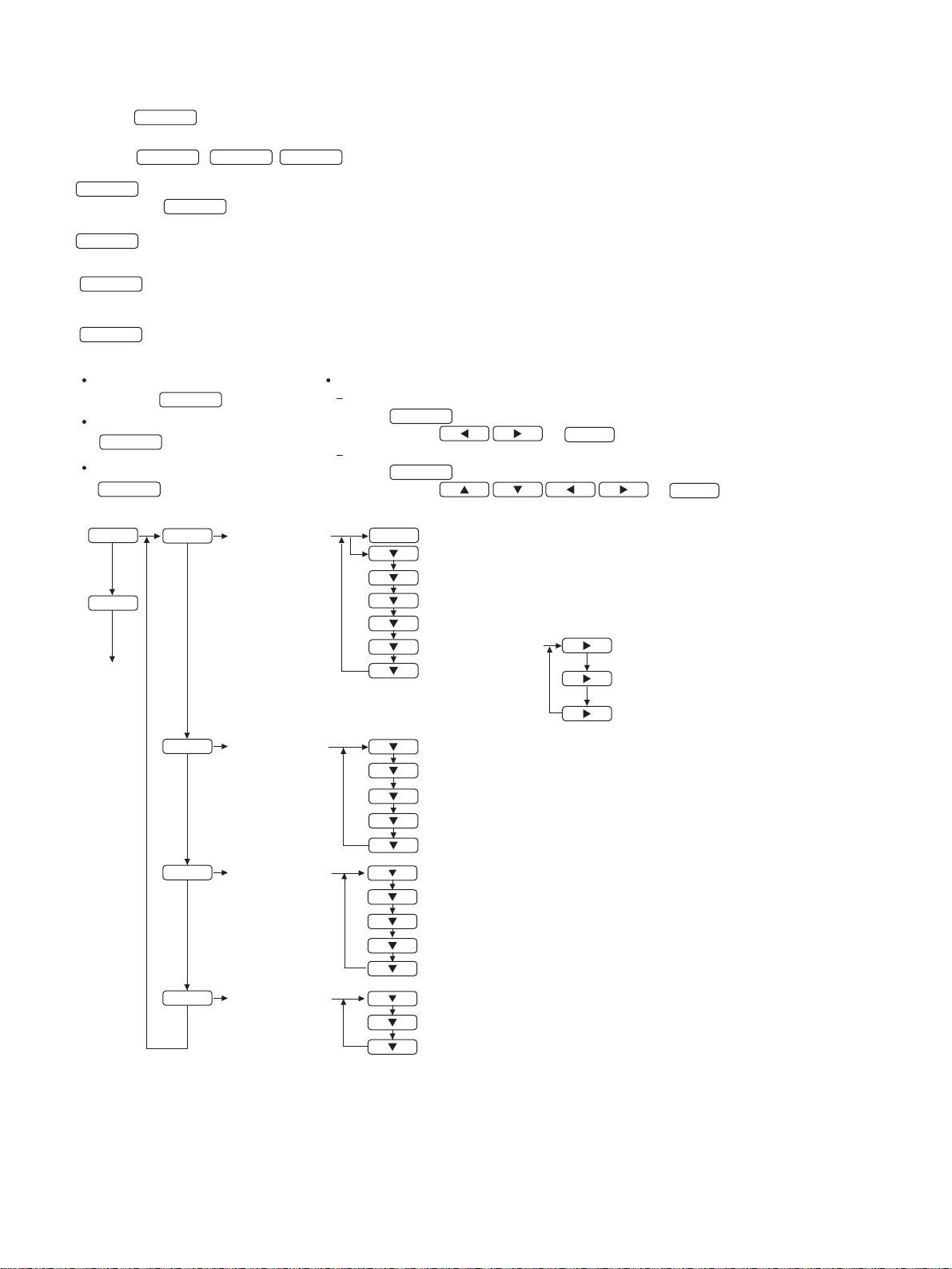
2. ADJUSTMENT
2-1. ADJUSTMENT METHOD (PC MODE)
* Press the PC button to select PC mode.
1) Resetting all adjustment values
Press the
MENU , , POWER buttons.
ENTER
2) Adjustment lock function
MENU
+ Power ON
(And press the button. )
d
3) INPUT
INPUT
CHANGE
4) VIEW MODE
VIEW MODE
PICT MODE
5)
PICT MODE
Watching two images simultaneously (PIP/SPLIT)
6)
CHANGE
CHANGE
Switching ON/OFF
Press the button.
ON/OFF
Selecting the active window
SELECT
to change the setting.
Swapping images (SWAP)
SWAP
7)
Adjustment pattern
MENU
MENU
to change the setting.
c
PICTURE MENU
END
AUDIO MENU
c
SETUP MENU
c
*
If you do not press any buttons for about 30 seconds
while in a menu screen, the settings you made up to
that point will be applied and the screen will
automatically disappear.
Adjusting the size or position of the small window
SIZE
When is pushed, "PIP Size" is displayed.
SIZE/MOVE
And press the .
+
ENTER
MOVE
When is pushed, "PIP Move"" is displayed.
SIZE/MOVE
And press the .
ENTER
AUTO
OPC
BRIGHTNESS
BLACK LEVEL
CONTRAST
(e d buttons)
(e d buttons)
(e d buttons)
(e d buttons)
COLOR CONTROL
RESET
+
ENTER
COLOR MODE
(STANDARD, sRGB, VIVID, TV/AV)
COLOR TEMP
(HIGH, MID-HIGH, MIDDLE MID-LOW, LOW, USER)
USER
(R-CONTRAST, G-CONTRAST, B-CONTRAST)
TREBLE
BASS
BALANCE
(e d buttons)
(e d buttons)
(e d buttons)
DOLBY VIRTUAL
RESET
AUTO SYNC
FINE SYNC
INPUT SIGNAL
SCALING
(e d buttons)
LANGUAGE
(bc buttons)
(bc buttons)
(bc buttons)
c
OPTION MENU
QUICK SHOOT
OUTPUT SELECT
DVI SELECT
LD-26SH3U CONNECTION, ADJUSTMENT, OPERATION, AND FUNCTIONS
2 – 7
Page 14
2-2. ADJUSTMENT ITEM LIST (PC MODE)
BUTTON ITEM ADJUSTMENT DESCRIPTION
MENU MENU 1:
PICTURE MENU
MENU 2:
AUDIO MENU
MENU 3:
SETUP MENU
AUTO
Automatically adjusts "Black Level" and "Contrast" based on the
brightest and darkest colors of the image displayed.
OPC
ON, OFF
Automatic the backlight brightness Adjustment.
Make sure no object obstructs the OPC sensor, which could
*
affect its ability to sense surrounding light.
BRIGHTNESS 0 ~ 31
Adjusts the backlight brightness.
If you adjust "Brightness" while "OPC" is "On", "OPC" is automati
cally set to "Off".
BLACK LEVEL 0~100 BLACK LEVEL: Total screen brightness can be adjusted
CONTRAST 0~100 CONTRAST: While watching the color pattern, adjustments can be
COLOR CONTROL Color Mode, Color
RESET Resets adjustment values for this menu to their original factory settings.
TREBLE -30~0~+30 Adjusts high-pitch sounds.
BASS -30~0~+30 Adjusts low-pitch sounds.
BALANCE -30~0~+30 Adjusts the balance between the right and left speakers.
DOLBY VIRTUAL ON/OFF Turns the Virtual Dolby Surround function "ON" or "OFF".
RESET Resets adjustment values for this menu to their original factory settings.
AUTO SYNC
FINE SYNC Clock, Phase,
INPUT SIGNAL 480 Lines,
SCALING 1~4
LANGUAGE
Temp.,
User : 0 ~255
H-Pos, V-Pos
768 Lines
English, French,
Spanish
Color Mode : Selects the color tone.
Standard : Displays images using the original color tone of the LCD
sRGB : sRGB is an international standard for color representation
Vivid : Displays images in vivid primary colors.
TV/AV : Provides a proper color tone to watch DVDs and TV
Color Temp. : Adjusts the color temperature (white balance).
High : Color tone bluer than "Middle".
Mid-High : Color tone slightly bluer than "Middle".
Middle : Standard setting for color tone.
Mid-Low : Color tone slightly redder than "Middle".
Low : Color tone redder than "Middle".
User : Allows you to individually adjust red, green, and blue
User : When "Color Temp." is set to "User", you can adjust red, green,
and blue contrast individually.
You can also set this item directly using the remote control, instead
of the adjustment screen.
Automatically adjusts "Clock", "Phase", "H-Pos.", and "V-Pos.".
Clock: Adjusts the clock so that no vertical flicker noise is
emitted.
Phase : Makes an adjustment after "Clock" is properly
H-Pos., V-Pos. : Adjusts the position of the adjustment pattern so
RESET : Resets the image's position to the monitor's
480 Lines : Specifies the horizontal resolution of a 480-line screen.
768 Lines : Specifies the horizontal resolution of a 768-line screen.
Adjusts the image to optimum sharpness when it is enlarged.
Selects the language (English, French or Spanish) on the screen.
while watching the color pattern. (
made so that all graduations appear. (
monitor.
defined by the IEC (International Electrotechnical Commission). Colors are converted by taking into account the
liquid crystal's characteristics and thereby represent color
tone close to the original image.
programs that are received from the computer
connected to the TV.
Set "Color Temp." to "Middle" if you want to display
all gradations.
contrast.
adjusted so that no horizontal flicker noise is emitted.
that it appears centered on screen.
original factory setting.
e d
buttons)
buttons)
e d
LD-26SH3U CONNECTION, ADJUSTMENT, OPERATION, AND FUNCTIONS
2 – 8
Page 15
BUTTON ITEM ADJUSTMENT DESCRIPTION
QS :
MENU
MENU 4:
OPTION MENU
QUICK SHOOT ON/OFF
OUTPUT SELECT F I XE D ,
VARIABLE1,
VARIABLE2
QUICK SHOOT
Reduces the visual lag inherent in fast-motion scenes.
Selects how to adjust the sound via the audio output terminals.
• FIXED : : Set "FIXED" when connecting to a VCR for
recording, etc.The volume is fixed.
Image and sound are simultaneously output via
the output terminals. (Image and sound are output via the output terminals a little earlier than
when image is displayed on the TV and sound is
output from the TV speakers.)
• VARIABLE1 : Set to enjoy the sound from both the TV speakers and external speakers while watching the
image on the TV, etc.
The volume can be adjusted.
Image is displayed on the TV at the same time
as when sound is output via the output terminals. (Sound is output via the output terminals a
little later than when image is output via the output terminal.)
• VARIABLE2 :
Set to enjoy only the sound from the external speakers while watching the image on the TV, etc.
The volume can be adjusted.
However, no sound can be heard from the TV
speakers with this setting. (Sound can be output
via the headphone terminal.)
Image is displayed on the TV at the same time
as when sound is output via the output terminals. (Sound is output via the output terminals a
little later than when image is output via the output terminal.)
DVI SELECT AV, PC Set depending on equipment connected to the DVI input terminal.
• A V : AV equipment (AV5 mode is available.)
• P C : Computer (PC DIGITAL mode is available.)r
For information on connecting to AV equipment or a computer.
LD-26SH3U CONNECTION, ADJUSTMENT, OPERATION, AND FUNCTIONS
2 – 9
Page 16
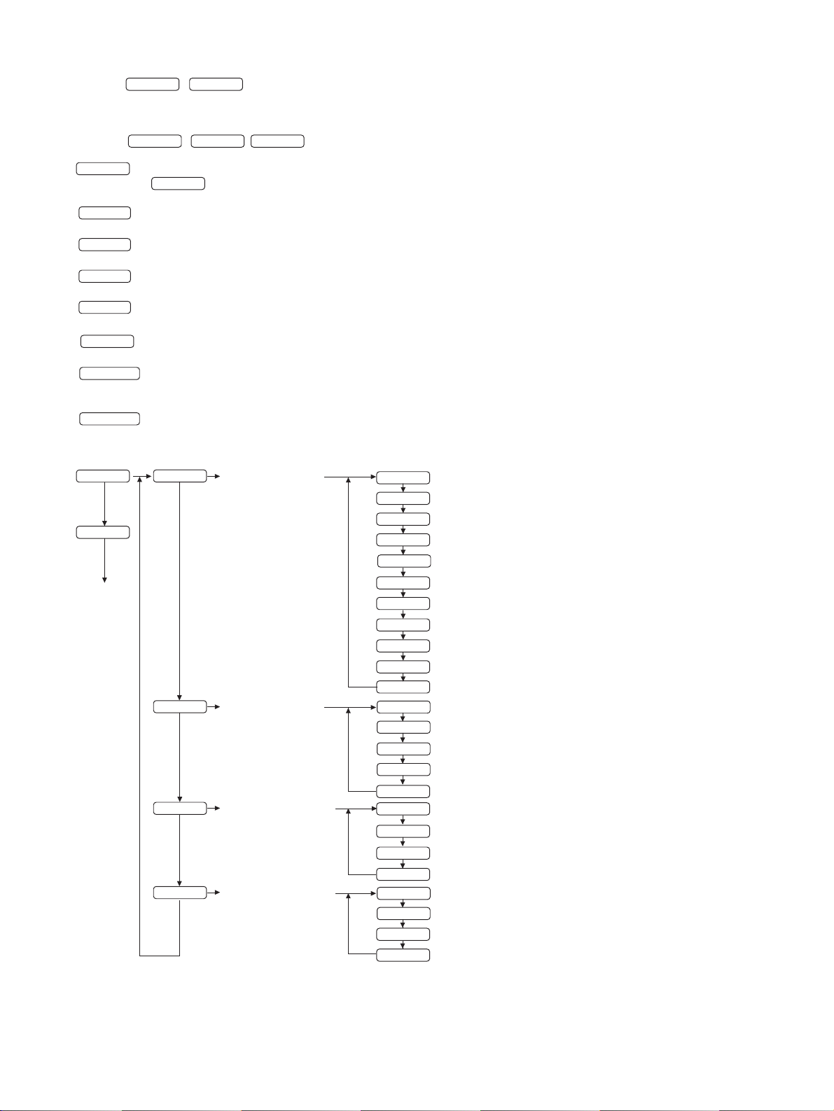
2-3. ADJUSTMENT METHOD (TV/AV MODE)
Press the
* /
*
If you do not press any buttons for about 30 seconds while in a menu screen, the settings you made up to
TV
that point will be applied and the screen will automatically disappear.
1) Resetting all adjustment values
Press the
MENU
ENTER
,
2) Adjustment lock function
MENU
(And press the button.)
+ Power ON
d
3) INPUT
INPUT
ON/OFF
4) PICT MODE
PICT
CHANGE
5) MUTE
MUTE
ON/OFF
6) MULTI CH TV SOUND
MTS
ON/OFF
7) VIEW MODE
VIEW MODE
CHANGE
8) SLEEP
SLEEP
to change the setting.
(The time changes in the following order each time you press the button)
9) CC
CC
to change the setting.
(The setting changes in the following order:)
10)
Adjustment pattern
MENU
MENU
END
c
c
c
c
button to select TV or AV, HDMI, DVI mode.
AV
,
POWER
buttons.
PICTURE MENU
AUDIO MENU
SETUP MENU
OPTION MENU
c
c
c
c
c
c
c
c
c
c
c
c
c
c
c
c
c
c
c
c
c
c
c
c
OPC
BRIGHTNESS
BLACK LEVEL
CONTRAST
COLOR
TINT
SHARPNESS
FLESH TONE
3D-Y/C
COLOR TEMP
RESET
TREBLE
BASS
BALANCE
DOLBY VIRTUAL
RESET
CH SETUP
V-C HI P
POSITION
LANGUAGE
QUICK SHOOT
OUTPUT SELECT
DVI SELECT
HDMI SETUP
(e d buttons)
(e d buttons)
(e d buttons)
(e d buttons)
(e d buttons)
(e d buttons)
(e d buttons)
(e d buttons)
(e d buttons)
(e d buttons)
(e d buttons)
LD-26SH3U CONNECTION, ADJUSTMENT, OPERATION, AND FUNCTIONS
2 – 10
Page 17
2-4. ADJUSTMENT ITEM LIST (TV/AV MODE)
BUTTON ITEM ADJUSTMENT DESCRIPTION
MENU MENU 1:
PICTURE MENU
MENU 2:
AUDIO MENU
MENU 3:
SETUP
OPC ON, OFF Automatic the backlight brightness Adjustment.
Make sure no object obstructs the OPC sensor, which could
*
affect its ability to sense surrounding light.
BRIGHTNESS
0 ~ 31 Adjusts the backlight brightness.
If you adjust "Brightness" while "OPC" is "On", "OPC" is automati
cally set to "Off".
BLACK LEVEL 0~100 Adjusts the overall brightness of the screen.
CONTRAST
0~63
Adjusts contrast.
COLOR -60~+60 Adjusts the color depth.
TINT -20~+20 Adjusts the color tone.
SHARPNESS 1~5 Adjusts the image quality.
FLESH TONE 1~5 Adjusts the flesh tone color.
3D-Y/C
Provides high quality images with minimal dot crawl and cross color
noise.
This adjustment is valid only for TV and images from the video input terminals (RCA pin).
Standard : Normal adjustment
Fast : For movie image
Slow : For still image
COLOR TEMP. Adjusts the color temperature (white balance).
High : Color tone bluer than "Middle".
Mid-High : Color tone slightly bluer than "Middle".
Middle : Standard setting for color tone.
Mid-Low : Color tone slightly redder than "Middle".
Low : Color tone redder than "Middle".
RESET
TREBLE
BASS
BALANCE
DOLBY VIRTUAL
-30~0~+30 Adjusts high-pitch sounds.
-30~0~+30 Adjusts low-pitch sounds.
-30~0~+30 Adjusts the balance between the right and left speakers.
ON/OFF Turns the Virtual Dolby Surround function "ON" or "OFF".
Resets adjustment values for this menu to their original factory settings.
You can also set this item directly using the remote control,
instead of the adjustment screen.
RESET
CH Setup
(TV mode only)
Resets adjustment values for this menu to their original factory settings.
Sets TV channels.
Air/Cable : Sets the receiving mode broadcast (Air) or cable TV
(Cable).
CH Search : Sets available channels automatically.
CH Memory : Sets channels manually.
V-Chip
Allows TV programs to be restricted and TV usage to be controlled based on FCC data.
MPAA : Sets whether MPAA block or unblock.
TV Guidelines : Sets whether TV Guidelines block or unblock.
Status : Sets whether the block setting status is on or off.
POSITION
-10~0~+10 Adjusts the position of the image.
V-POSITION : Adjusts the image's vertical position.
H-POSITION : Adjusts the image's horizontal position.
RESET : Resets the image's position to the monitor's original
factory setting.
Language
English, French,
Spanish
Selects the language (English, French, or Spanish) on the
screen.
LD-26SH3U CONNECTION, ADJUSTMENT, OPERATION, AND FUNCTIONS
2 – 11
Page 18

BUTTON ITEM ADJUSTMENT DESCRIPTION
MENU
MENU 4:
OPTION
QUICK SHOOT ON, OFF
QS :
QUICK SHOOT
Reduces the visual lag inherent in fast-motion scenes.
Output Select Selects how to adjust the sound via the audio output terminals.
• FIXED : : Set "FIXED" when connecting to a VCR for
recording, etc.The volume is fixed.
Image and sound are simultaneously output via
the output terminals. (Image and sound are output via the output terminals a little earlier than
when image is displayed on the TV and sound
is output from the TV speakers.)
• VARIABLE1 : Set to enjoy the sound from both the TV
speakers and external speakers while watching the image on the TV, etc.
The volume can be adjusted.
Image is displayed on the TV at the same
time as when sound is output via the output
terminals. (Sound is output via the output terminals a little later than when image is output
via the output terminal.)
• VARIABLE2 :Set to enjoy only the sound from the external
speakers while watching the image on the TV,
etc.
The volume can be adjusted.
However, no sound can be heard from the TV
speakers with this setting. (Sound can be output via the headphone terminal.)
Image is displayed on the TV at the same
time as when sound is output via the output
terminals. (Sound is output via the output terminals a little later than when image is output
via the output terminal.)
DVI SELECT Set depending on equipment connected to the DVI input terminal.
A V : AV equipment (AV5 mode is available.)
P C : Computer (PC DIGITAL mode is available.)
For information on connecting to AV equipment or a computer.
HDMI Setup
(AV4 mode only)
Sets the parameters related with HDMI setting.
Signal Type : Selects the signal type from the HDMI input
terminal.
Unless the image quality looks obviously poor,
select "Auto".
Color Matrix : Selects the internal color space conversion
method when an RGB signal is input. Normally,
select "Auto".
Dynamic Range : Selects the signal amplitude range. Normally,
select "Standard".
Auto View : Sets whether or not to use "View Mode" based
on signal recognition, including an HDMI signal.
LD-26SH3U CONNECTION, ADJUSTMENT, OPERATION, AND FUNCTIONS
2 – 12
Page 19
2-5. BUTTON SPECIFICATIONS LIST
ADJUSTMENT Function
Main unit buttons INPUT TV,AV1, AV2, AV3, AV4, AV5, PC (Digital), PC
MENU Displaying the images in MENU mode.
ENTER
CH
b
CH
c
VOL
d
VOL
e
POWER Turning power on/off.
Remote control
buttons
MENU Displaying the images in MENU mode.
1 2 3 4
ENTER The item of the menu is decided.
RETURN Returns to the previous screen.
EXIT Exits the MENU screen.
POWER Turning power on/off.
INPUT TV,AV1, AV2, AV3, AV4, AV5, PC (Digital), PC
TV Switching TV mode.
AV AV1
PC PC (Analogue)
Channel 0 ~ 9, 100 Selecting channels
CH
b
CH
c
VOL
+
VOL
-
MUTE Muting the sound.
MTS Selecting Multi ch TV Sound.
FLASHBACK Returning to previous channel
CC Off
FREEZE Pausing the screen.
PIP/SPLIT ON/OFF Displaying the images in PIP/Split mode.
SIZE/MOVE
SWAP In PIP/Split mode, you can switch the images
SELECT Selecting the active window.
VIEW MODE TV/AV mode:
PICT MODE TV/AV mode: STANDARD
DISPLAY Checking your TV's current settings
SLEEP Off
(Analogue)
(Analogue)
AV2 3 AV3 3 AV4 3 AV5 Switching AV mode.
3
PC (Digital) Switching PC mode.
3
CC1 3 CC2 3 Text1 3 Text2 3 Off... Setting the Closed Caption.
3
Side Bar, S. Stretch, Zoom, Stretch
PC mode : Normal, Stretch
DYNAMIC 3
3
GAME 3 USER 3
CINEMA
STANDARD...
PC mode : STANDARD
3
150 min 3 Off
STANDARD...
30 min 3 60 min 3 90 min 3 120 min
3
USER 3
3
Switching display modes
Select item of the menu and set content is decided.
Selecting channels
Adjusting increase of the volume.
Adjusting decrease of the volume.
Selects an item by moving the cursor
up/down/left/right.
Switching display modes
Selecting channels
Adjusting increase of the volume.
Adjusting decrease of the volume.
Adjusting the size or position of the small window.
displayed on two windows with each other.
Changing the screen size.
Adjusting the picture mode.
Switching power off after a specified length of time.
3
LD-26SH3U CONNECTION, ADJUSTMENT, OPERATION, AND FUNCTIONS
2 – 13
Page 20
2-6. TOOL FOR SERVICE
(1) ALL RESET
Resetting all the adjustment values to the default values
Press and hold [MENU] button and [ENTER] button on the monitor,
1
turn on the power of the machine. Keep pressing the buttons until
"All resetting" is displayed on the screen.
After completion of all reset, boot the machine in the TV mode.
2
Press the power button of the machine to turn off the power.
3
Caution:When the power button is pressed after that, "EZ SETUP"
is booted.
(2) Version display (for service)
Press and hold down both the [M EN U] button and the [ d ] button on the sys-
1
tem unit while pressing the [POWER] button on the system unit, to turn on the
power supply of the system. Hold the three buttons down until the version is
displayed on screen.
The farmware version and checksum appears on screen.
2
Turn off the power supply of the system or terminate the display by
3
pressing the [MENU] button on the system unit.
VERSION & CHCK SUM
VERSION
CHECK SUM
CUSTOM MODE
DEMO MODE
MODEL
MODEL:
Model, Size, and Destination are displayed in this order from the left.
Model LD : LD-26SH3U
Size 32 : 32 inch
26 : 26 inch
Destination JP : For Japan
US : For United State of America
(3) AGING (FOR SERVICING)
Press and hold [ENTER] button and [e] button of the monitor, and
1
press the power button to turn on the power at the same time. Keep
pressing the three buttons until "AGING TEST MENU" is displayed.
"AGING TESTMENU" is displayed.
2
AGING TEST MENU
AGING TEST 1
AGING TEST 2
Select an item with [b][c] buttons of the machine.
3
Press [ENTER] button of the main unit. The selected test is performed.
4
■ Ageing test 1: The screen is switched over in the following manner:
DARK BLUE
BLUE3GREEN3RED3WHITE3 BLACK
■ Ageing test 2: Every time the [
Press the power button of the main unit to terminate the operation.
5
the screen is switched over as follows:
WHITE3BLACK3RED3GREEN3BLUE3WHITE50%
1.01 (20050101)
:
: OK ABCD
: OFF
: OFF
: LD 26 US
END : MENU
SET : ENTER END : MENU
DARK GREEN3DARK RED
3
] (VOL) button is pressed,
d
3
3
(4) Color balance initializing (for servicing)
In the following cases, initialize the color balance.
*
• When the LCD panel is replaced.
• When the main PWB is replaced.
• When Part No. U707 is replaced.
Press and hold [ENTER] button and [e] button on the monitor, turn
1
on the power button of the machine. Keep pressing the three buttons until "AGING TEST MENU" is displayed.
"AGING TEST MENU" is displayed.
2
AGING TEST MENU
AGING TEST 1
AGING TEST 2
On "AGING TEST MENU" press and hold [e] button and [d] button
3
simultaneously together.
"SERVICE MENU " is displayed.
4
SERVICE MENU
MODEL CHANGE
COLOR TEMPERATURE
Use [b][c] buttons of the machine to select " COLOR TEMPERATURE ."
5
Press [ENTER] button of the machine.
6
"COLOR TEMPERATURE" is displayed.
7
COLOR TEMPERATURE
<PC> R G B
High 236 243 255
⇒
Mid-High 245 248 255
Middle 2 55 255 255
Mid-Low 2 55 238 209
Low 255 249 237
<TV/AV>
High 236 243 255
Mid-High 245 248 255
Middle 255 246 231
Mid-Low 255 238 209
Low 255 2 49 237
RESET
Use [b][c] buttons of the machine to select "RESET".
8
Press [ENTER] button of the machine.
9
The display color of "RESET" is changed in the sequence of Yellow
White 3Yellow. Then initializing is completed.
3
Turn off the power of the machine.
F
3
SET : ENTER END : MENU
SET : ENTER END : MENU
END:MENU
LD-26SH3U CONNECTION, ADJUSTMENT, OPERATION, AND FUNCTIONS
2 – 14
Page 21
2-7. LD-26SH3U FLASH WRITING PROCEDURE
The software programs required to be written into the LD-26SH3U are
the flash data (firmware) and the EDID data (for DDC).
Write the data according to the following procedures.
1. Write down the channel setting data and the menu adjustment data,
if necessary.
2. Write the flash data (firmware) into the LD-26SH3U.
3. Write the EDID data into the LD-26SH3U.
(When U45/U47/U49/U50 is (are) changed.)
The EDID data are divided into the following four kinds. Use the
*
three writing tools to write them.
EDID data Writing tool
1 U47 (PC-DIGITAL)
2 U45 (PC-ANALOG)
3 U49 (HDMI) EDID (HDMI)
4 U50 (DVI-AV) EDID (DVI-AV)
4. Perform ALL RESET.
All the adjustment values including the channel setting are reset.
*
5. Check the version.
6. Set the adjustment values recorded in the step 1 to the LD-26SH3U,
if necessary.
EDID (PC)
[Operating procedure by use of a jig]
(1) Connect the jig to the PC. (Refer to the separate document.)
(2) Execute c:\fg\launcher.exe
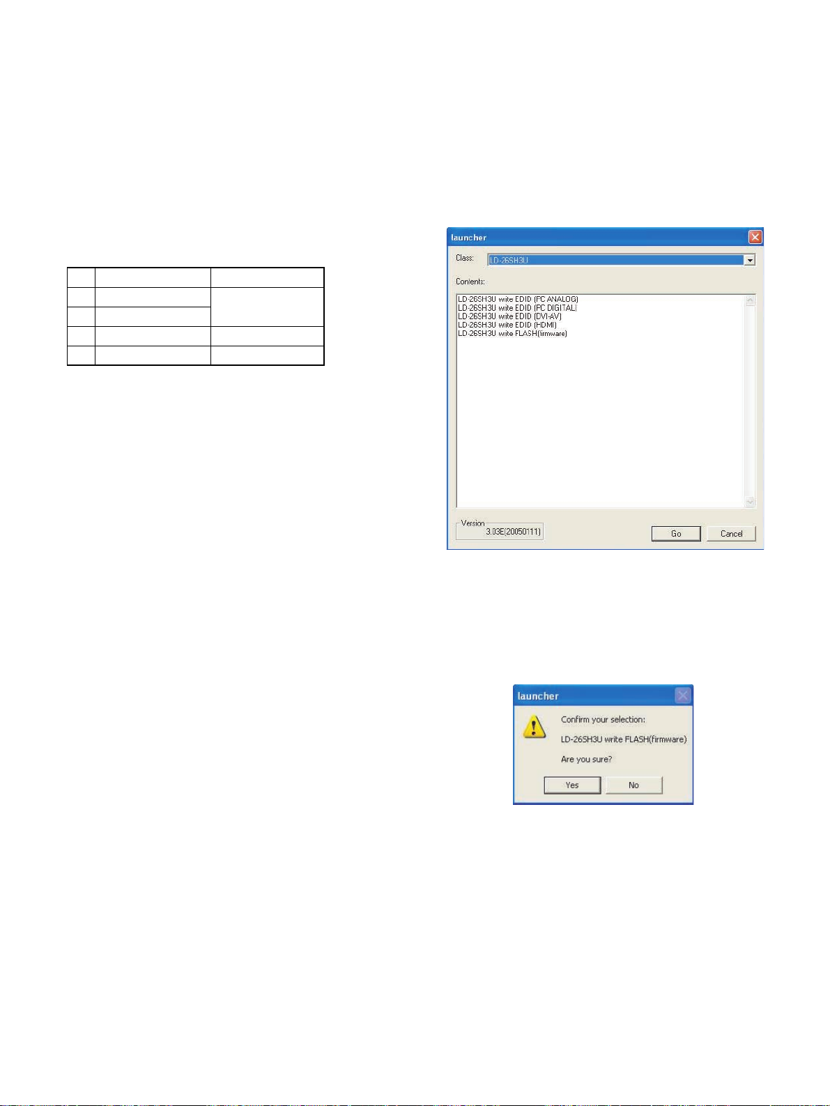
(3) The window below is displayed. Select the suitable item from [Clas-
sification] and [Process content] according to the target model.
Select the target model in [Classification].
Select [XXXXXXXX (target model) write FLASH (firmware)] from
[Process content].
[Tool target model]
LD-26SH3U
[Tool operating environment]
• Windows 98/Windows 2000/Windows XP
(For use of USB cable, Windows 2000/Windows XP)
[Installing procedure]
(1) Create a folder, c:\fg.
(2) Copy all the files in the launcher tool FD to c:\fg.
(Use a launcher tool of the latest version.)
(3) Copy all the files in the flash writing tool FD to c:\fg.
(4) Double-click "install.bat" in c:\fg. (If the MS-DOS prompt does not
disappear automatically, delete it manually.)
(5) Copy all the files in the flash writing data FD to c:\fg.
(If data in the FD are compressed, decompress them before use.)
There are two kinds of operating procedures: the operating procedure
by use of a conventional jig, and the operating procedure by use of a
USB cable instead of a jig.
After selection, press [GO] button.
The confirmation window is shown. If the content is OK, press [Yes];
and if not, press [No]. When [No] is pressed, the procedure returns to
(3). If [Yes] is pressed, the procedure goes to the next step.
When a button is pressed, the window display is switched.
LD-26SH3U CONNECTION, ADJUSTMENT, OPERATION, AND FUNCTIONS
2 – 15
Page 22
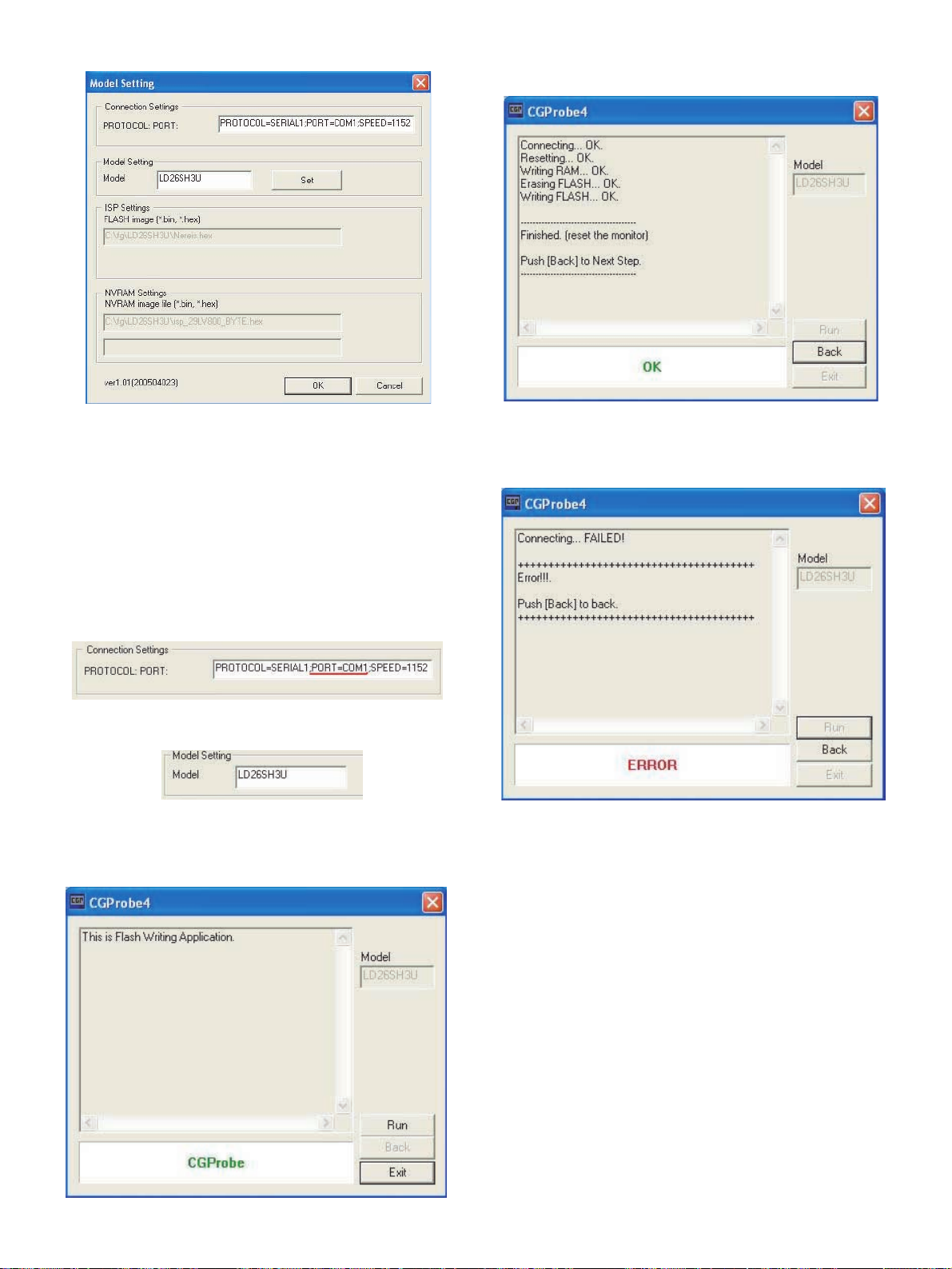
(4) The following window is displayed. Connect the jig to the monitor.
(7) When writing is completed, the following window is displayed. "Fin-
ished. (reset the monitor)" is displayed.
[Setting on the monitor side]
1 : Connect the VGA cable to the jig.
2 : Press and hold [Channel select
[Volume
] on the main unit, and press [Power] key at the
e
] and [Volume d] and
c
same time. Wait until [ISP MODE] is displayed. After confirming that [ISP MODE] is displayed, press [ENTER] key.
[Setting on the writing tool side]
Perform the PORT setting of Connection Settings. (The figure shows
a case where COM1 port is used. When COM4 is used, write as
"PORT=COM$:".) Once it is set, it is saved.
(5) Check the model name.
After checking, press [OK] button.
(6) The following window is displayed.
Press [Run] button, and flash writing is started.
(8) If an error in writing occurs, the following window is displayed.
("Error!!!" is displayed.) Check connection between the PC and the
monitor, and retry writing.
(9) After normal completion of writing, press [Power] key of the monitor
to turn off the power.
(10) When [Back] button is pressed after normal completion of writing,
the display returns to the screen of step (6), allowing writing into
another set. Press and hold [Channel select
[Volume
] on the main unit, and press [Power] key at the same
e
time. Wait until [ISP MODE] is displayed. After confirming that [ISP
MODE] is displayed, press [ENTER] key. Then repeat procedures
from step (6).
(11)
To terminate flash writing, press [Back] button and press [Exit] button.
] and [Volume d] and
c
LD-26SH3U CONNECTION, ADJUSTMENT, OPERATION, AND FUNCTIONS
2 – 16
Page 23
[Operating procedure by use of a USB cable]
To use a USB cable is used, the driver must be installed.
*
(Refer to the separate document, "USB serial driver installing procedure.")
(1) Connect the monitor and the PC with a USB cable. (Refer to the
separate document.)
(2) Execute c:\fg\launcher.exe.
(3) The following window is displayed. Select a suitable item in [Classi-
fication] and [Process content].
Select the target model from [Classification].
Select "XXXXXXXX(Target model)write FLASH(firmware)" from
[Process content].
After selection, press [GO] button.
(4) The following window is displayed.
[Setting on the monitor side]
Press and hold [Channel select c] and [Volume d] and [Volume e]
on the main unit, and press [Power] key at the same time. Wait until
[ISP MODE] is displayed. After confirming that [ISP MODE] is displayed, press [ENTER] key.
[Setting on the writing tool side]
Perform the PORT setting of Connection Settings.
Check the COM port number on the device manager window.
(Refer to the separate document, "USB serial driver installing procedure.")
(The figure shows a case where COM1 port is used. When COM4
is used, write as "PORT=COM$:.") Once it is set, it is saved.
The confirmation window is shown. If the content is OK, press
[Yes]; and if not, press [No]. When [No] is pressed, the procedure
returns to (3). If [Yes] is pressed, the procedure goes to the next
step.
When a button is pressed, the window display is switched.
(5) Check the model name.
After checking, press [OK] button.
(6) The following window is displayed. Press [Run] button, and flash
writing is started.
LD-26SH3U CONNECTION, ADJUSTMENT, OPERATION, AND FUNCTIONS
2 – 17
Page 24
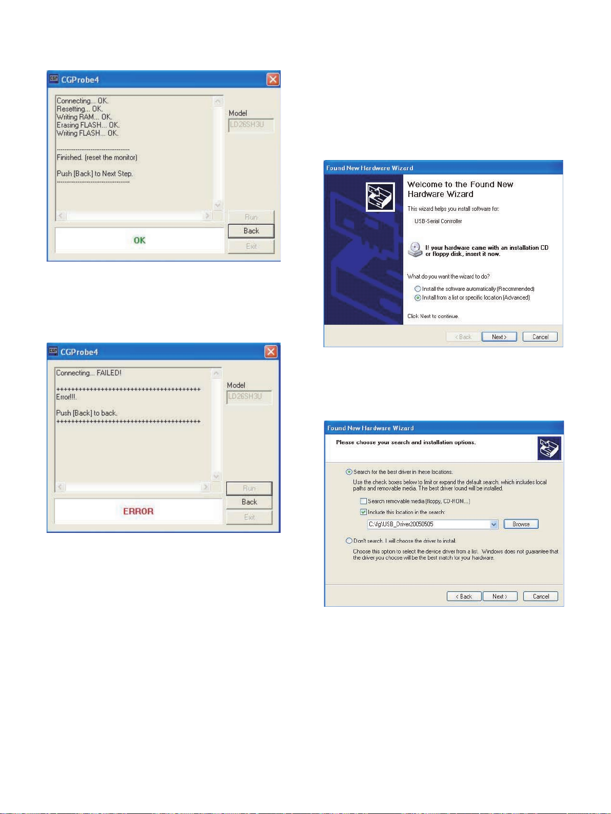
(7) After completion of writing, the following window is displayed.
"Finished. (reset the monitor)" is displayed.
(8) If an error in writing occurs, the following window is displayed.
("Error!!!" is displayed.) Check connection between the PC and the
monitor, and retry writing.
[USB serial driver installing procedure]
To use a USB cable for flash writing, this driver must be installed.
*
If a jig is used for flash writing, this driver is not required
*
(1) Copy the USB serial driver file to c:\fg, and decompress it in the
same folder.
(2) Connect the PC and the monitor with a USB cable (AB type).
(Terminal A is on the PC side, terminal B on the monitor side.)
The following window is displayed.
(9) After normal completion of writing, press [Power] key of the monitor
to turn off the power.
(10)When [Back] button is pressed after normal completion of writing,
the display returns to the screen of step (6), allowing writing into
another set. Press [Power] key to turn on the power, and repeat procedures from step (6).
[Install from the list or a specified location] and press [Next].
(3) The following window is displayed.
Check [The following location is included.], and click [Refer] to
specfy th folder where the USB serial driver was decompressed.
Press [Next].
(11)
To terminate flash writing, press [Back] button and press [Exit] button.
LD-26SH3U CONNECTION, ADJUSTMENT, OPERATION, AND FUNCTIONS
2 – 18
Page 25
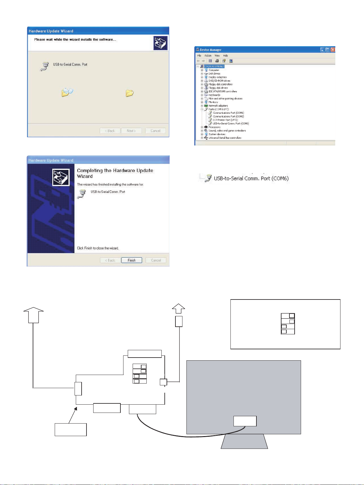
(4) The following window is displayed, and installation is started.
(5) After completion of installation, the following window is displayed.
(6) Check the COM port. Open the property of my computer, click
[Hardware] tab, and click [Device manager] tab. The following window is displayed.
Check the COM number of [USB-to-Serial Comm. Port] on the window.
Use this COM port number for flash writing.
Press [Complete] to close the window.
LD-26SH3U FLASH WRITING TOOL CONNECTION DIAGRAM [WHEN JIG IS USED]
Connect to USB port of PC
Connect to PC serial port.
Serial connector
No need to connect parallel cable.
Parallel connector
PWB
DVI-D
connector
VGA connector
USB Terminal A
䌕䌓䌂㩷㪺㪸㪹㫃㪼
USB Terminal B
LD-26SH3U
Back surface of the machine
X1049MP-27
VGA cable
DIS switch direction
SW1: Parallel
SW2: AUTO MANUAL
SW3: 1502A T1620
SW4: 1502A T1620
Right, Right, Left, Left from the top when viewed
from the parallel connector
VGA
terminal
(EDID)
Serial (PROGRAM)
LD-26SH3U CONNECTION, ADJUSTMENT, OPERATION, AND FUNCTIONS
2 – 19
Page 26
LD-26SH3U FLASH WRITING TOOL CONNECTION DIAGRAM (When USB cable (AB type) is used instead of a jig)
Connect USB port of PC
USB Terminal A
䌕䌓䌂 cable
LD-26SH3U
Back surface of machine
USB Terminal B
2-7. LD-26SH3U EDID Writing Procedures
The software data which must be written with the IT-32M2 are the flash
data (firmware) and EDID (data for DDC).
Perform the writing procedures below.
1. Write down the adjustment values such as the channel setting and
the custom mode setting (special specifications), if necessary.
2. Write the flash data (firmware).
3. Write the EDID data. (When U45/U47 is changed.)
4. Perform initialization.
All the adjustment values are reset including the channel setting
*
and the custom mode setting.
5. Check the version.
6. Restore the adjustment values saved in step 1 to the machine, if
necessary.
[Tool target model]
LD-26SH3U
[Tool operating environment]
• Windows95/Windows98/Windows 2000/Windows XP
• Set the I/O address of the printer port to 378.
(Refer to the supplemental descriptions.)
[Installing procedures]
(1) Create a folder, c:\fg.
(2) Copy all the files in the launcher tool to c:\fg.
If there is a folder for the launcher tool, use that folder.
(Be sure to use the latest-version launcher tool.)
(3) Copy all the files in the EDID writing tool of the LD-26SH3U servic-
ing to c:\fg.
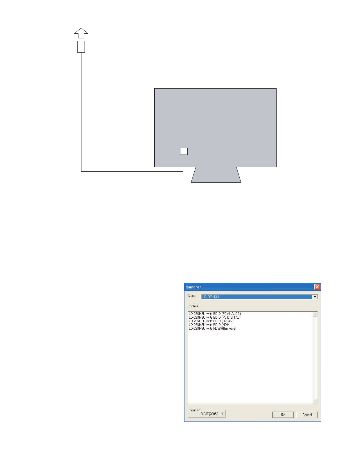
[Operating procedures]
(1) Connect the jig to the PC. (Refer to the separate document.)
(2) Execute c:\fg\launcher.exe.
(3)The window below is displayed.
Select a target model from [Classification].
Select "XXXXXXXX (target model) write EDID" from [Process content].
After selection, click [EXECUTE].
In this model (LD-26SH3U), PC analog EDID and PC digital EDID,
*
DVI-AV EDID, HDMI EDID writing must be performed individually.
Select "XXXXXXXX (target model) write EDID (PC ANALOG)" or
"XXXXXXXX (target model) write EDID (PC DIGITAL)",
"XXXXXXXX (target model) write EDID (DIVI-AV)",
"XXXXXXXX (target model) write EDID (HDIM)" depending on
the case.
LD-26SH3U CONNECTION, ADJUSTMENT, OPERATION, AND FUNCTIONS
2 – 20
Page 27
(4) The confirmation window is displayed. If it is OK, press [YES]. If not,
press [NO]. When [NO] is pressed, the process returns to step (3).
When [YES] is pressed, the process goes to the next step.
[Monitor side setting (for PC analog EDID writing)]
1 : Connect the RGB cable with the monitor and the jig.
2 : Press [POWER] key to turn on the power.
[Monitor side setting (for PC digital EDID writing)]
1 : Press [POWER] key of the monitor to turn on the power.
2 : Press [MENU] key to display MENU OSD. Press [
shift the cursor to [Option], and press [
shift to [DVI Select].
3 : Press [Enter] key, and press [
selection] OSD to switch to [PC]
(It is set to [AV] when shipping from the factory.)
4 : Connect the DVI-D cable to the monitor and the jig.
[Monitor side setting (for DVI-AV EDID writing)]
1 : Press [POWER] key of the monitor to turn on the power.
(If the monitor is not in the TV mode, press [INPU] key to set it
to the TV mode.)
2 : Press [MENU] key to display MENU OSD, and press [
shift the cursor to [Option]. Press [
to [DVI Select].
3 : Press [Enter] key, and press [
tion] OSD to switch to [AV]
(It is set to [AV] when shipping from the factory.)
4 : Connect the DVI-D cable to the monitor and the jig.
[Monitor side setting (for HDMI EDID writing)]
1 : Connect the DVI-HDMI cable to the monitor and the jig.
2 : Press [POWER] key to turn on the power.
(5) When the following window is displayed:
] key in [Input terminal
d
.
] key in [Input terminal selec-
d
.
] key three times to
c
] key three times to shift it
c
] key to
d
d
] key to
(6) The following window is displayed. Connect the jig to the monitor.
Check the model name.
(7) Enter the serial number with 10-key, and press [NEXT].
When writing HDMI and DVI-AV EDID, there is no need to enter
*
the serial number. EDID writing is automatically performed.
(8) The following window is displayed.
• When writing PC analog EDID
• When writing PC digital EDID
The jig is not connected with the PC properly.
Check the connection, press [OK], and press [NEXT].
LD-26SH3U CONNECTION, ADJUSTMENT, OPERATION, AND FUNCTIONS
2 – 21
Page 28
• When writing DVI-AV, HDMI EDID
On this window, EDID writing and verifying are performed.
If the operation is terminated halfway, connection may be improper.
Check connection.
After completion of writing, the window of step (6) is displayed.
Connect the jig to the following monitor.
Repeat the EDID writing procedures fro, step (6) for the monitor.
In this model (LD-26SH3U), when one operation of EDID writing
*
is completed, click [CANCEL] on the window of item (6) to terminate the writing tool and return to item (2). Then perform writing
another EDID. Be sure to write all kinds of EDID data.
(9) Error in writing or verifying
[Supplemental description]
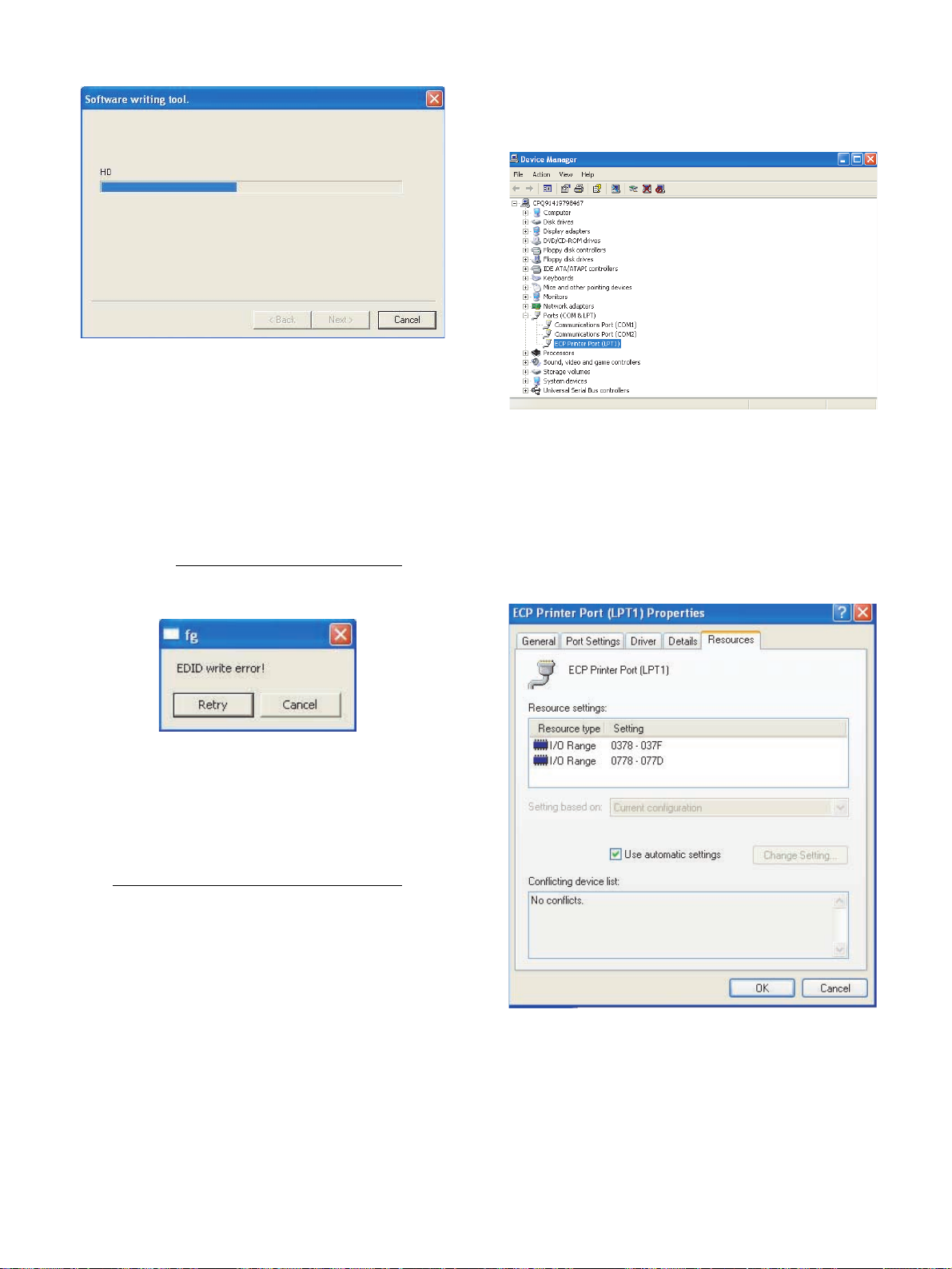
How to set the printer port I/O address to 378:
❍
1. Open the system property from the control panel.
2. Open the device manager tag, and check "Display by type (T)."
3. Click "+" on the left of "PORT (COM/LPT)" to check that "Printer
port (LPT1)" is displayed. (The display may be slightly different,
such as "ECP printer port (LPT1).")
4. Open the property of the printer port (LPT1), and open the resource
tag.
5. Uncheck "Automatic setting" and select "Basic setting 0000.
(If "I/O range" is already set to "0378 - 037F," there is no need to
change.)
In case of an error in writing or verifying, the above window is displayed.
When [RETRY] button is pressed, writing and verifying of EDID are
performed again. For normal cases, check the cable connection
and press this button.
If an error still occurs in retry, press [CANCEL] button. If [Cancel]
button is pressed, the process is forcibly advanced to the next window, but note that the EDID data are not written properly
(10)When writing is completed normally or when [CANCEL] button is
pressed on the EDID error window, the display goes to the window
of step (6). Then writing of another set can be performed.
(11)Press [Power] button to turn off the power.
.
❍ In the above descriptions, the copy destination folder of the files is
c:\fg. This folder may be any folder in the hard disk as long as all the
files are copied to the same folder.
LD-26SH3U CONNECTION, ADJUSTMENT, OPERATION, AND FUNCTIONS
2 – 22
Page 29
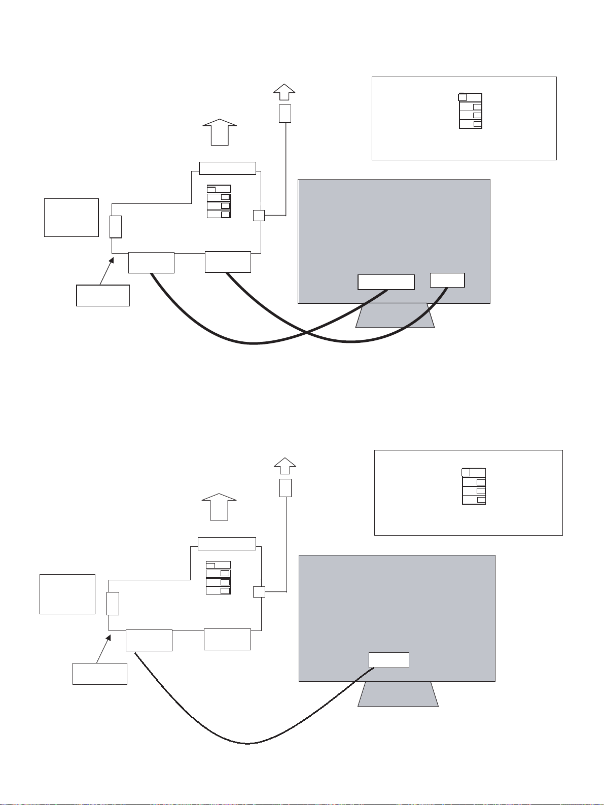
LD-26SH1U EDID (PC-ANALOG) date writing tool connection diagram
Noޓneed
toconnect
serialcable
X1049MP-27
DIP switch direction
Connect to PC printer port
Parallel connector
Serial connector
PWB
DVI-D
connector
DVI-D cable
VGA
connector
USB
Connect to PC
USB port.
䌕䌓䌂 cable
VGA cable
Back surface of the machine
SW1: Parallel (EDID) Serial(PROGRAM)
SW2: AUTO MANUAL
SW3: 1502A T1620
SW4: 1502A T1620
Left, Right, Right, Right from the top when viewed
from the parallel connector
LD-26SH3U
DVI terminal
VGA
terminal
LD-26SH3U EDID (PC-DIGITAL) date wr iting tool connection diagra m
USB
Noޓneed
toconnect
serialcable
X1049MP-27
Serial connector
DVI-D
connector
Connect to PC printer port
Parallel connector
PWB
VGA
connector
DVI-D cable
Connect to PC
USB port.
䌕䌓䌂 cable
DIP switch direction
SW1: Parallel (EDID) Serial(PROGRAM)
SW2: AUTO MANUAL
SW3: 1502A T1620
SW4: 1502A T1620
Left, Right, Right, Right from the top when viewed
from the parallel connector
LD-26SH3U
Back surface of the machine
DVI terminal
LD-26SH3U CONNECTION, ADJUSTMENT, OPERATION, AND FUNCTIONS
2 – 23
Page 30

LD-26SH3U EDID (DVI - AV) date writing tool connection diagram
Noޓneed
toconnect
serialcable
X1049MP-27
Serial connector
DVI-D
connector
Connect to PC printer port
Parallel connector
PWB
DVI-D cable
USB
VGA
connector
DIP switch direction
Connect to PC
USB port.
䌕䌓䌂 cable
Back surface of the machine
SW1: Parallel (EDID) Serial(PROGRAM)
SW2: AUTO MANUAL
SW3: 1502A T1620
SW4: 1502A T1620
Left, Right, Right, Right from the top when viewed
from the parallel connector
LD-26SH3U
DVI terminal
LD-26SH3U EDID (HDMI) date writing to ol c onnection diagram
Noޓneed
toconnect
serialcable
Serial connector
DVI-D
connector
Connect to PC printer port
Parallel connector
PWB
VGA
connector
USB
X1049MP-27
DVI-D cable
Connect to PC
USB port.
䌕䌓䌂 cable
DIP switch direction
SW1: Parallel (EDID) Serial(PROGRAM)
SW2: AUTO MANUAL
SW3: 1502A T1620
SW4: 1502A T1620
Left, Right, Right, Right from the top when viewed
from the parallel connector
LD-26SH3U
Back surface of the machine
HDMI terminal
LD-26SH3U CONNECTION, ADJUSTMENT, OPERATION, AND FUNCTIONS
2 – 24
Page 31

CHAPTER 3. DISASSEMBLY AND ASSEMBLY
1. STAND UNIT DISASSEMBLY
1. Remove the I/O cover lower
1. Remove two screws 2, and remove the hinge cover rear 3.
2. Remove four screws
4
1
, and remove the stand unit 5.
4
2
4
4
1
3
3. MB PLATE UNIT DISASSEMBLY
1. Remove two screws 1, and remove I/O inner cover 2 is removed.
2. Remove each screw
plate unit
5
.
and fan motor harness 4, and remove the MB
3
3
5
3
4
3
3
3
2
1
1
3
4. KEY PWB UNIT/HEADPHONE PWB UNIT
DISASSEMBLY
1. Remove two screws 1 and harness 2, and remove the key PWB unit
.
3
2. Remove two screw
and remove the headphone PWB unit
, harness 5 and earth cable fixing screw 6,
4
.
7
2. BACK COVER DISASSEMBLY
1. Remove the I/O cover 1.
2. Remove each screw
Caution: Be careful not to break the support stick.
3
, and remove the back cover 3.
2
2
2
2
2
2
2
2
1
5
2
1
3
4
7
6
LD-26SH3U DISASSEMBLY AND ASSEMBLY
3 – 1
Page 32

5. BASE PLATE L/R DISASSEMBLY
7. LCD UNIT DISASSEMBLY
1. Remove each screw 1, and remove base plate R 2 .
2. Remove each screw
, and remove base plate L 4.
3
1
1
1
2
1
4
1. Remove the screw 1, and remove the LCD unit 2.
1
2
3
1
1
3
3
2
6. LCD ASSEMBLY DISASSEMBLY
1. Remove the harness 1 and each screw 2, and remove LCD assembly
.
3
3
2
2
2
1
LD-26SH3U DISASSEMBLY AND ASSEMBLY
3 – 2
Page 33

CHAPTER 4. TROUBLE SHOOTING
LD-26SH3U TROUBLE SHOOTING
4 – 1
Page 34

LD-26SH3U TROUBLE SHOOTING
4 – 2
Page 35

LD-26SH3U TROUBLE SHOOTING
4 – 3
Page 36

CHAPTER 5. BLOCK DIAGRAM
GM1501
R,L
DVI AUDIO
VPC3230D Y/C
VPX3226F Y/C
Y, Pb, Pr
uPD64084 OUTPUT Y/C
PC AUDIO
R,L
VPX3226F
ITU656, 8 BIT
Z86129
TA1287FG
CVBS OUT
VPC3230
FLI2310BD
R,G,B
ITU656, 8 BIT
MST9883C
FOR COMPONENT INPUT C.C.
HDMI Connector
SiI9011
ITU 601, YCbCr, 16 BIT
ITU 601, YCbCr, 16 BIT
RGB, 24 BIT
DC5V
LVDS
32" LCD
CTRL
12V
CTRL
KEYPAD
+
PWR BTN
CONNECTOR
DVI
TMDS
G, R, B, HS, VS
CRT
G, R, B, HS, VS
TMDS
uP
PSU
USB HUB POWER CONNECTOR
MAIN TO IT RECIEVER
CONNECTOR
GM1501 RST#
GM1501 ON
PSON#
PSON
POWER ON
CONTROL PANEL
LED+
IR+OPC
CONNECTOR
IR
FOR PANEL
FOR SYSTEM
OPC
MINI USB
PL2303X
RS232
USB
I2S
SIMULATED IR
t
r
r
a
1. BLOCK DIAGRAM
TV
AV1,AV3 (S2)
AV1,AV3 (RCA composite)
AV2 Conponent input
AV2 input, AV output (composite)
Key Pad board
IO borard
TV input, output
U 8
AV1,AV3 (S2) input terminal
J5
AV1, AV3 (composite) input terminal
J7
AV1 D4 input terminal
J7
AV2 input, AV output (composite) terminal
J20
J3
32 inch LCD Panel
LQ255T3LZ25 with Inverter
FAN
CN1 CN2
CN5
CN201
CN202
J19 J10
Power supply
unit
DPS-213DP
J13
J17
J11
J4
Main board
J8
J14
J17
J22
J30 J31J32
J28
J29
J34J24
1-1. Main PWB
MAIN BD TO IO BD
R,L
R,L
VPX3226F Y/C
VPC3230D Y/C
Connector 1
uPD64084 OUTPUT Y/C
MAIN BD TO IO BD
Connector 2
MAIN TO IT RECIEVER
CONNECTOR
+5V
USB HUB POWER CONNECTOR
DVI AUDIO
2
PC AUDIO
2
Y, Pb, Pr
HDMI Connector
I2S
CRT
DVI
3
.
.
G, R, B, HS, VS
TMDS
Headphon board
VPX3226F
2
2
3
TA1287FG
FOR COMPONENT INPUT C.C.
MST9883C
SiI9011
HDMI/DVI(HDCP)
SIMULATED IR
J1
2
Speake
ITU656, 8 BIT
VPC3230
Cb2/Y2/Cr2
R1/G1/B1
VOUT
3
CVBS OUT
R,G,B
.
Z86129
ITU 601, YCbCr, 16 BIT
ITU 601, YCbCr, 16 BIT
(R)
Speake
ITU656, 8 BIT
(L)
.
LED board
8
16
5
LD-26SH3U BLOCK DIAGRAM
5 – 1
FLI2310BD
J701
8
G, R, B, HS, VS
TMDS
USB
input
RGB, 24 BIT
HDMI
input
24
AUDIO
input
GM1501
2
RS232
PL2303X
2
MINI USB
PC
Degit
input
DC5V
LVDS
CTRL
12V
CTRL
ADC
USB
PC
Analog
input
GM1501 RST#
32" LCD
PANEL
INVERTER
LQ255T3LZ11
CONTROL PANEL
DDR SDRAM
128Mbit
ROM
8Mbit
PC
Sound
input
FOR PANEL
+24V
FOR SYSTEM
+12V
+5V
+3V
+5V_SB
GM1501 ON
IR
OPC
KEYPAD
+
PWR BTN
CONNECTOR
.
AC inpu
PSU
PSON#
PSON
uP
POWER ON
LED+
IR+OPC
CONNECTOR
Page 37

䋨
1-2. I/O PWB
123
123
13
4
4
12
5
5
11
6
6
10
7
9
7
4
5
6
FD13
FD_DOT040
1
FD2
FD_DOT040
1
8
9
8
ANG ANG ANG
7
MTG12
MTG11
ID4.5/OD8.0
ID4.5/OD8.0
123
12
11
10
9
8
MTG15
ID4.5/OD8.0
ANG ANG
FD14
FD713
FD_DOT040
FD_DOT040
1
1
FD3
FD702
FD_DOT040
FD_DOT040
1
1
123
8
IO_GND
12
11
10
9
MTG14
ID4.5/OD8.0
123
7
9
8
IO_GND
13
12
11
10
MTG18
ID4.5/OD8.0
4
5
6
7
8
TVTUNER_GND
123
12
11
10
9
MTG19
ID4.5/OD8.0
AV OUT
AV1
AV2
AV3
TV
Tuner
AV1
YPbPr
AV2
YPbPr
IT RECEIVER
YPbPr
R,L
SIF
2
CVBS
R,L
Y/C,CVBS
R,L
CVBS
2
R,L
Y/C,CVBS
R,L
CVBS
MSP4441K
3
2
3
2
R,L
Y, Pb, Pr
Y, Pb, Pr
Y, Pb, Pr
I2S_DEL_OUT
I2S_DEL_IN
CXA2069Q
Video Switch
3
3
3
Right
Left
Right
Left
3
I2S
3
I2S
CIN
Y/CVBS_IN
SM5301CS-G
SM5301CS-G
Level
shift
LPF
LPF
LPF
LPF
YDA138
LM4911
NJU26901
AUDIO DELAY
Buffer
uPD64084A
3D Y/C
uPD64031
GR
TO
HEADPHONE
Level
shift
Speaker
SV_C_3230
SV_Y3230
LPF
3
Y, Pb, Pr
3226 Y/C
2
3D_Y/C
Connector
123
13
12
11
10
4
5
6
FD714
FD_DOT040
1
FD703
FD_DOT040
1
4
12
5
11
6
10
7
7
9
8
MTG13
ID4.5/OD8.0
123
13
4
12
4
5
11
5
6
10
6
7
9
8
MTG17
ID4.5/OD8.0
1-3. POWER PWB
EM I Filter
AC Input
Relay
EM I Filter
+Rectifier
FL3)
䋨
EM I Filter
+Rectifier
PFC
DCM
Converter
PFC controller
(IC1)
AC Brown out
DC Brown out
(IC2)
VCC Supply
(Q901)
(IC902)
Back Up converter
Fly back PWM
(IC904)
(IC802)
LLC Converter
LLC controller(IC801)
+5Vsb Feedback
+5Vsb O/P Rectifier
PS-ON, OVP, OCP, OTP
Main loop Feedback
+24V O/P rectifier
+12V O/P Rectifier
+5.2V Loop Feedback
+5.2V Linear Regulator
+3.3V D2D Converter
+3.3V Loop FB䋨IC301)
& O VP
+5VSB*1.5A
PS-ON
+24V*5A
+12V*4A
+5.2V*5.5A
+3.3V* 3A
Primary Secondary
LD-26SH3U BLOCK DIAGRAM
5 – 2
System interface
Page 38

2. CONNECTOR TABLE
■ MAIN PWB TARMINAL
J8
1GND
2LOCK_FAN1
3 +8V_FAN
J10
1 +12V_P
2 +3.3V_P
3 +3.3V_P
4GND
5GND
6 +5V_P
7 +5V_P
8GND
9GND
10 +5V_SB_P
11 +5V_SB_P
12 GND
13 GND
14 PSON#
J11
1 INPUT
2MENU
3OK
4 CHANNEL_UP
5 CHANNEL_DOWN
6 VOLUME_UP
7 VOLUME_DOWN
8 AOS_SET#
9POWER
10 HOTEL_DETECT
11 GND
12 NC
J24
1 REDU+
2 GREENU+
3BLUEU+
4NU
5GND
6GND
7GND
8GND
9+5V
10 GND
11 NU
12 A-SDA
13 A-HS
14 A-VS
15 A-SCL
J14
1 Y/CVBS_OUT_3226
2GND
3 C_OUT_3226
4GND
5 SV_C_3230
6GND
7 3D_C_3230
8GND
9 SV_Y_3230
10 GND
11 3D_Y_3230
12 GND
13 Pb_OUT
14 GND
15 Y_OUT
16 GND
17 Pr_OUT
18 GND
19 PC_LINE_INL
20 GND
21 PC_LINE_INR
22 GND
23 DVI_AUDIO_INL
24 GND
25 DVI_AUDIO_INR
26 GND
J18
1VFC_PWM
2GND
3 TUNER_AFT
4GND
5 DEV_RESET2#
6 TUNER_I2C_SW
7AMP_MUTE
8AV_SW_MUTE
9HP_MUTE
10 GND
11 HDMI_WS_9011
12 HDMI_SDO_9011
13 HDMI_CLK_9011
14 GND
15 D_MODE_DEL
16 GND
17 MSTR_SDA
18 MSTR_SCL
19 GND
20 +5VS_DIG
21 +5VS_DIG
22 +5V_VD
23 +5V_VD
24 AV_SW_MUTE_2
25 +3V_VD
26 +9V_VD
LD-26SH3U BLOCK DIAGRAM
5 – 3
Page 39

J19
39 SELLVDS LVDS_RL 40
37 GND LVDS_UD 38
35 TXA3+ GND 36
33 TXA3- LVDS_FRAME 34
31 GND LVDS_O_Sset 32
29 TXAC+ GND 30
27 TXAC- LVDS_Temp3 28
25 GND LVDS_TEST3 26
23 TXA2+ GND 24
21 TXA2- LVDS_Temp2 22
19 GND LVDS_Temp1 20
17 TXA1+ GND 18
15 TXA1- GND 16
13 GND GND 14
11 TXA0+ GND 12
9TXA0- GND10
7 GND BACKLIGHT_ADJUST 8
5 GND BACKLIGHT_ENABLE 6
3+5V +5V4
1+5V +5V2
J34
■ I/O PWB
J4
J5
J22
OPTICAL_SENSOR_LED
1
3 OPC_OUT_ADC
NETWORK_WIRELESS_ON
5
7 NETWORK_WIRE IR_DATA_IN 8
9 +5V LED2_KEYPAD 10
11 GND GND 12
+MICRO_P_3.3V 2
NETWORK_WIRELESS_SET
LED_KEYPAD 6
4
1GND
2 PC_LINE_INL
3GND
4 PC_LINE_INR
5GND
1 +12V_SPEAKER
2 +12V_SPEAKER
3 +12V_GND
4 +12V_GND
1Y GND
2C GND
3 SVIDEO1_L_IN
4 SVIDEO1_C_IN
5GND
6 IO_AV1_S_DETECT
7Y GND
8C GND
9 SVIDEO3_L_IN
10 SVIDEO3_C_IN
11 IO_AV3_S_DETECT
J28
J29
1 +USB_5V
2USB_D3 +USB_3.3V
4 USB_D+
1RX2IN2RX2IN+
3GND
4NU
5NU
6 DVISCL
7 DVISDA
8NU
9RX1IN10 RX1IN+
11 GND
12 NU
13 NU
14 DVI_5V
15 GND
16 DVI_CAB
17 RX0IN18 RX0IN+
19 GND
20 NU
21 NU
22 GND
23 RXCIN+
24 RXCIN-
J7
1GND
2 RCA_V1
3 IO_AV1_RCA_DETECT
4 RCA_V3
5 IO_AV3_RCA_DETECT
6GND
7 RCA_IN_L1
8 RCA_IN_L3
9GND
10 RCA_IN_R1
11 RCA_IN_R3
J20
1GND
2 RCA_V2
3 IO_AV2_RCA_DETECT
4 RCA_V3
5 IO_AV_OUT_DETECT
6GND
7 RCA_IN_L2
8 CONN_OUT_L
9GND
10 RCA_IN_R2
11 CONN_OUT_R
LD-26SH3U BLOCK DIAGRAM
5 – 4
Page 40

J13
J17
1 IO_Y/CVBS_OUT_3226
2GND
3 IO_C_OUT_3226
4GND
5 IO_SV_C_3230
6GND
7 IO_3D_C_3230
8GND
9 IO_SV_Y_3230
10 GND
11 IO_3D_Y_3230
12 GND
13 IO_Pb_OUT
14 GND
15 IO_Y_OUT
16 GND
17 IO_Pr_OUT
18 GND
19 IO_PC_LINE_INL
20 GND
21 IO_PC_LINE_INR
22 GND
23 IO_DIGITAL_INL
24 GND
25 IO_DIGITAL_INR
26 GND
1 IO_VFC_PWM
2GND
3 IO_TUNER_AFT
4GND
5 IO_DEV_RESET#
6IO_HP_MUTE
7 IO_TUNER_I2C_SWITCH
8 OUT_MUTE
9 IO_YDA138_MUTE
10 GND
11 IO_HDMI_WS
12 IO_HDMI_SDO
13 IO_HDMI_SCL
14 GND
15 IO_D_MODE
16 GND
17 IO_MSTR_SCL
18 IO_MSTR_SDA
19 GND
20 +IO_5V
21 +IO_5V
22 +ANG_5V
23 +ANG_5V
24 IO_AVSWITCH_MUTE
25 +ANG_3.3V
26 +9V_VIDEO
J16
1 Y1_IO D1_LINE_1 8
2 GND D1_I/P_D 9
3 PB1_IO REV2 10
4 GND D1_RATIO 11
5 PR1_IO GND 12
6 GND REV3 13
7 REV1 PLUG1_DET 14
J23
1 Y2_IO D2_LINE_1 8
2 GND D2_I/P_D 9
3 PB2_IO REV2 10
4 GND D2_RATIO 11
5 PR2_IO GND 12
6 GND REV3 13
7 REV1 PLUG2_DET 14
J31
1
2
L+
L-
J30
1R+
2R-
J32
1HPOL
2 HP VOC
3HPOR
4 +ANG_5V
LD-26SH3U BLOCK DIAGRAM
5 – 5
Page 41

■ SUB PWB
J1
1HP_L
2 HP VOC
3HP_R
4DET_HP
J3
1 INPUT
2MENU
3OK
4 CHANNEL_UP
5 CHANNEL_DOWN
6 VOLUME_UP
7 VOLUME_DOWN
8 AOS_SET#
9POWER
10 HOTEL_DETECT
11 GND
12 NC
J22
1 OPTICAL_LED +MICRO_P_3.3V 2
3OPC_OUT
NETWORK_WIRELESS__LED_ON
5
7 NETWORK_WIRE_LED IR_DATA_IN 8
9 +5V LED2_KEYPAD 10
11 GND GND 12
NETWORK_WIRELESS_SET
LED_KEYPAD 6
4
LD-26SH3U BLOCK DIAGRAM
5 – 6
Page 42

CHAPTER 6. HARDWARE DESCRIPTION
1. CIRCUIT DESCRIPTIONS
1-1. TV TUNER U8 (VT2W8JW553)
The VT2W8JW553 is a TV tuner of NTSC system.
The power voltage is inputted from 5V (3 pin).
Tuning control is performed with I2C bus (10, 11pin), and video signals (1Vpp) is passed to 17pin and to the composite video signal switch IC (U33).
Audio SIF FM signal (about 50mVp-p) is outputted to 14pin, and passed
through the SIF filter to the audio processor U5.
When the electric field strength exceeds 60dB, the AGC voltage output
(7pin) falls below 4.5V. This voltage is used for auto tuning, and 12
channels of stronger waveforms are selected and saved in the memory.
The AFT voltage output (12pin) becomes about 2.5V when tuning is
correctly performed. (100kHz/1V)
This voltage is controlled by the microprocessor to be 2.5V for performing correct tuning.
The antenna output pin is used to connect a ground wave digital tuner.
To use the antenna output pin, an AC adapter must be connected.
1-2. VIDEO SIGNAL PROCESS
1-2-1. AV input selector U33 (CXA2069Q)
This is an AV selector IC to select audio signals and video signals from
the external composite video signal input pin, S pin input, and the TV
tuner. Switch control is made with I2C at 33 and 34pin.
The output composite signal is supplied through the 3-dimentional Y/C
separation IC (U17) and the ghost reduction IC U11 (UPD64031A) to
the video decoder U24 (VPC3230D). The input from S pin is directly
supplied to U24.
1-2-2. Ghost reduction U11 (UPDA)
The UPD64031A reduces ghost phenomena which appear at the back
(on the right side) or in front of tuner images made by jamming waves of
different transmission distances reflected by buildings, etc.
Under an environment of clear waveforms without ghost, it is better to turn
off the ghost reduction for slightly clear images. ON/OFF control of the
ghost reduction can be made with [GR] button on the remote control unit.
The composite signal outputted from the AV input selector U33 is inputted to the ghost reduction U11 134pin, and outputted from 6 ~15pin as
digital composite signals, and then inputted to the 3-dimentional Y/C
separation U17.
When the ghost reduction is turned OFF, the signals are supplied
directly to the 3-dimentional Y/C separation U17 without passing
through this IC.
1-2-3. 3-dimentional Y/C separation U17 (UPD64084)
The UPD64084 is a Y/C separation IC which separates brightness
signals and color signals from the composite video signals which are
mixed with brightness signals such as tuner video and color signals.
Composite video signals outputted from the AV input selector U33 (53pin)
are passed through the low-pass filter circuit and inputted to 93pin.
Brightness signals are Y/C-separated and outputted from 89pin (AYO).
Color signals are outputted from 88pin (ACO) and passed through the
low-pass filter (U16) and the band pass filter (U21), and supplied to the
video decoder (U24).
1-2-4. Video decoder U24 (VPC3230D)
This is a video decoder IC which converts Y/C separation signals into
digital Y/Pb/Pr signals. Composite video signals inputted from the tuner
and the external input pin are Y/C-separated and inputted to 75pin and
72pin. Y/C signals from S pin are inputted directly to 74pin and 71pin
and processed as S signals and converted into digital Y/Pb/Pr signals
and outputted. The output is passed to the IP conversion U15.
1-2-5. IP conversion U30 (FLI2310)
The FLI2310 performs IP conversion of interlace digital Y/Pb/Pr signals
from the video decoder (U24) into progressive digital RGB signals, and
performs IP conversion of digital RGB signals from U32 and supplies
them to the scaler U34.
1-2-6. Scaler & CPU U34 (gm1501)
The gm1501 allows direct input of analog RGB signals/digital DVI signals for PC, and converts digital RGB signals from U42 into signals
according to the specified screen size, and outputs LVDS signals to the
LCD module.
It is also provided with microprocessor functions to control many IC’s
according to information from the flash memory (U42).
In addition, its additional function provides the PinP (Picture in Picture)
function of PC inputs, tuner inputs, and external video inputs, changes
the frame rate, and performs the OSD (On-Screen Display) function.
1-3. AUDIO SIGNAL PROCESS
1-3-1. Audio processor U5 (MSP4441K)
This is an audio processor to process audio signals.
The MSP4441K decodes SIF signal inputs (67pin) of the tuner output to
suitable stereo or monaural format, performs sound quality setting by
Bass or Treble, decodes stereo signals to virtual Dolby surround signals,
performs the sound volume setting depending on each input source,
and performs other processes of the audio signal system.
It also selects external input signals (56, 57pin) selected by the input
selector U33 (CXA2069Q) and PC audio inputs (47, 48pin), performs
the ready ray process, and provides outputs from 27 and 28pin to the
speaker amplifier and outputs from 24 and 25pin to the headphone
amplifier.
It also provides outputs from 36 and 37pin through the input selector
U33 (CXA2069Q) to the external output pin.
1-3-2. Digital audio display U4 (NJU26901)
This delay IC delays the output time for audio signals.
When an audio signal is inputted to 1pin, it is subjected to delay process
for the specified time and outputted to 7pin.
1-3-3. Speaker driver U48 (YDA138)
This is a digital power audio amplifier IC of the BTL system.
It drives a speaker of 8 ΩΩΩΩ at the maximum output of 10W x 2.
Audio signals inputted at 5 and 38pin are outputted through the LC filter to
8 and 14 pin (Rch) and 29 and 35 pin (Lch) of the speaker as PWM signals.
The voltage gain is determined by the voltage at 26 and 27pin. By grounding the both pins, the gain is set to 36dB.
When the control voltage at 6pin is grounded, sounds are muted.
1-3-4. Headphone amplifier U12 (LM4911)
This is an audio power amplifier which allows gain adjustment with an
external resistor.
Headphone signals inputted from 1 and 5pin are outputted to 7 and 9pin
(L and R channels).
LD-26SH3U HARDWARE DESC RIPTION
6 – 1
Page 43

1-4. INVERTER UNIT (RDENC220TPZZ)
This is an inverter unit for lighting the 18 backlights (straight tubes
CCFT) of the LCD panel. It allows ON/OFF control and brightness
(DUTY light control system).
The power for operations is provided directly from the power unit 24V
output connector (CN201) for the inverter through the cable.
The J19 connector 6pin in the main PWB is used for ON/OFF control
(ON at 5V) of the backlights, and 8pin is used for the control voltage of
brightness adjustment.
Brightness is the maximum at 0V. The higher the voltage is, the darker
the brightness is. (Max. voltage: 5V)
The protection circuit is provided to terminate the circuit operation to
protect against a trouble in the lamp.
Note: The inverter unit provides a high voltage of max. 2100V to the
lamp by means of the boosting transformer.
Use a great care not to move your hands close to the output connector, etc. when conducting, because it is extremely dangerous.
Be careful when repairing.
1-5. AC POWER UNIT (DPS213DP)
This is the power unit of overall output of 213W of multi outputs (24V, 12V,
5V, 3.3V/5V, sub). The input power specification is AC100 ~ 240V (50/60Hz).
This is provided with the AC input output, the inverter output connector
CN201, and the other I/O connector CN202.
The output of 24V for the inverter is passed to CN201.
The voltage of 24V is provided to 1pin ~ 10pin, and 11pin ~ 20pin are
grounded.
CN202 1, 2, and 5pin are for 12V for the circuit.
5 and 6pin are for 5V for the circuit.
10 and 11 pin are for 3.3V for the circuit.
16 and 17pin are for 5V for the sub power source.
15pin is for ON/OFF control input PSON.
18pin is for the power source status output PG.
The other pins (3, 4, 8, 9, 12, 13, 14, 15pin) are grounded.
When the AC power is inputted, 5V of the sub power is outputted. The
other power voltages are outputted when the CN202 ON/OFF control
pin is driven to LOW level. When the output is provided, the power status signal becomes HIGH.
5V and 3.3V are generated from 12V in the power source by the DC-DC
converter circuit. The protection circuits are provided for an overvoltage,
an overcurrent, and a high temperature. When the power is shut down,
remove and insert the AC power cord to restore the power.
Note: During AC input, a voltage is provided to the radiating plates
(HS1, HS2, HS4) on the primary side of the power unit. Be careful of an electric shock when repairing.
(The radiating plate HS3 near the output connector is at GND
level and has no problem.)
Though an AC input is interrupted, electric charges may remain
in the internal capacitor. Use enough care for that.
1-6. REMOTE CONTROL
This is a remote control of the infrared ray system. When the remote
control key is pressed, infrared rays are emitted in pulses. (Remote control code)
When the remote control light receiving section U13 attached to the
front of the unit receives infrared ray pulses, it converts infrared rays into
a voltage, and sends information to the microprocessor for proper operation.
LD-26SH3U HARDWARE DESC RIPTION
6 – 2
Page 44

B
B
B
D
D
D
D
1/22
12345678
12345678
12345678
12345678
C
C
C
C
B
0.1U
50V
C297
0603
+5V_VD
12
TP715
1
834
OS
VCC
GND
A0A1A2
SDA
SCL
U27
LM75_SO
P/N = 284500751203
SO8
76512
GND GND
1 2
1 2
A
21
21
21
21
I2C address: 90
R254 33 0603
R253 33 0603
FD709
FD_DOT040
FD9
FD_DOT040
For thermal QS.
MSTR_SCL_5(3,15)
MSTR_SDA_5(3,15)
For ESD
1
TP724
TOUCHPAD_METAL16
10
11
12
MTG7
ID4.5/OD8.0
9
1
238
7
456
10
11
12
MTG6
ID4.5/OD8.0
9
1
238
7
MTG5
ID4.5/OD8.0
456
10
11
12
1
238
456
9
7
FD712
FD_DOT040
FD12
FD_DOT040
1
1
1
1
1
TP723
TOUCHPAD_METAL16
1
MTG9
ID4.5/OD8.0
GND GND
Close to D-SUB Close to DVI
GND
3
3
3
3
CHAPTER 7. CIRCUIT DIAGRAM & PWB LAYOUT
1. CIRCUIT DIAGRAM
Project name :26SH3U PCB version : R02
1-1. MAIN PWB
D
D
D
D
FD710
FD_DOT040
FD10
FD_DOT040
1
1
C
C
C
C
FD711
FD_DOT040
FD11
FD_DOT040
1
1
MTG4
ID4.5/OD8.0
MTG3
ID4.5/OD8.0
10
11
12
1
238
456
10
111213
1
238
456
9
7
9
7
LD-26SH3U CIRCUIT DIAGRAM & PWB LAYOUT
7 – 1
GND GND GND GNDVD_GND
FOR ESD
87654
87654
87654
87654
B
B
B
B
A A
A A
A A
A
Page 45

B
B
B
D
D
D
D
2/22
12345678
12345678
12345678
12345678
PSON#
PSON
PSU
C
C
C
C
uP
POWER ON
+
PWR BTN
CONNECTOR
KEYPAD
B
LED+
IR+OPC
CONNECTOR
A
.
IR
OPC
21
21
21
FOR PANEL
+24V
FOR SYSTEM
+12V
+5V
+3V
+5V_SB
8
GM1501 ON
PANEL
26" LCD
GM1501 RST#
LVDS
DC5V
CTRL
24
RGB, 24 BIT
INVERTER
12V
CTRL
GM1501H
LQ255T3LZ11
CONTROL PANEL
DDR SDRAM
128Mbit
ROM
8Mbit
G, R, B, HS, VS5TMDS
ADC
RS232
2
USB
USB
2
PL2303X
21
3
3
3
3
ITU656, 8 BIT
26SH3U System Block Diagram
VPX3226F
DVI AUDIO
2
R,L
MAIN BD TO IO BD
FLI2310BD
8
16
.
ITU656, 8 BIT
CVBS OUT
VOUT
R1/G1/B1
Cb2/Y2/Cr2
VPC3230
2
2
2
3
.
3
PC AUDIO
2
VPC3230D Y/C
VPX3226F Y/C
R,L
Y, Pb, Pr
uPD64084 OUTPUT Y/C
Connector 1
R,G,B
Z86129
3
.
TA1287FG
FOR COMPONENT INPUT C.C.
.
MAIN BD TO IO BD
ITU 601, YCbCr, 16 BIT
ITU 601, YCbCr, 16 BIT
SiI9011
HDMI/DVI(HDCP)
MST9883C
HDMI Connector
Connector 2
2.VPC3230D Y/C--->VPC3230D--->FLI2310BD--->GM1501
3.uPD64084 OUTPUT Y/C--->VPC3230D--->FLI2310BD--->GM1501
4.YPbPr--->VPC3230D--->FLI2310BD--->GM1501 (D1, C.C. OFF)
1.VPX3226F Y/C--->VPX3226F-->GM1501
SIMULATED IR
TMDS
G, R, B, HS, VS
I2S
DVI
CRT
MAIN TO IT RECIEVER
CONNECTOR
+5V
6.YPbPr---->AD9883C--->FLI2310--->GM1501 (D2~D4)
7.HDMI--->SiI9011--->FLI2310--->GM1501
5.YPbPr--->TA1287--->VPC3230--->Z86129--->TA1287--->VPC3230
--->FLI2310--->GM1501 (D1, C.C. ON)
87654
87654
87654
USB HUB POWER CONNECTOR
87654
B
B
B
D
D
D
D
C
C
C
C
LD-26SH3U CIRCUIT DIAGRAM & PWB LAYOUT
B
A A
A A
A A
A
7 – 2
Page 46

B
B
B
P/N = 283468470001
0.1U/NA
C7
0603
12
Q7
DDTC144WCA/NA
3
2
HDCP_SW
C
C
C
C
50V
GND
+5V
RESERVED FOR HDCP KEY
1
GND
DEBUG PORT
+5V
C531
12
1U
FOR I2C PORT
0603
J33
123456789
GND
FLASH_DETECT
FLASH_DETECT(6,17)
12
R603
10K
0603
MSTR_SCL_5
MSTR_SDA_5
+MICRO_P_3.3V
RESET_MICRO_P
10
11
MICRO_P_RXD
MICRO_P_TXD
RESET_MICRO_P(17)
MICRO_P_RXD(17)
MICRO_P_TXD(17)
GND1
GND2
MA/11PX1/RA
ACES
D
D
D
D
3/22
12345678
12345678
12345678
12345678
123
A0A1A2
VCCWPSCL
U707
876
+3.3V
0.1U
50V
C879
0603
12
GND
R504
10K
0603
12
+3.3V
MSTR_SCL_1601
3
4
GND
SDA
5
MSTR_SDA_1601
Q63
GND
M24C64
SO8
P/N = 283430100001
DDTC144WCA
2
NVRAM_SW
+3.3V
U1
1
GND
123
A0A1A2
SDA
567
+3.3V
SCLK
4
GND
WC-
VCC
8
R25
10K/NA
12
M24C02/NA
0603
GND
SO8_1
+3.3V
NVRAM
87213-1100
P/N = 291000021109
GND
CC_INT (15)
B
+3.3VS_DIG
+3.3VS_DIG
+3.3V
I2C BUS
R814
10K
12
R819
10K
12
R505
12
R810
10K
12
R809
10K
12
MSTR_SDA (10,12,13,14,16,19)
MSTR_SCL (10,12,13,14,16,19)
MSTR_SDA
MSTR_SCL
0603
0603
PCA9515_SW
R261
10K
0603
12
R239
10K
0603
12
U708
237
1B
1A
1
MSTR_SCL_1601
MSTR_SDA_1601
6
2B
2A
584
1C
VCC
+3.3V
2C
GND
SN74LVC2G66
C8841U25V
12
+5V_VD +5V_VD
US8
0603
+3.3VS_DIG
P/N = 284574266001
GND
10%
10K
0603
0603
0603
A
MSTR_SDA_5 (1,15)
MSTR_SCL_5 (1,15)
21
21
21
MSTR_SDA_5
MSTR_SCL_5MSTR_SCL
Q34
2N7002
DS
DS
D
D
S
S
Q31
2N7002
G
G
MSTR_SDA
21
3
3
3
3
OCMADDR3
OCMADDR4
OCMADDR2
AA3
OCMADDR4
OCMADDR3
VGRN5
VGRN6
B21
A21
C21
GREEN_HD6
GREEN_HD7
GREEN_HD5
+3.3V
OCMADDR0
OCMADDR1
AA2
AA1
OCMADDR2
OCMADDR1
OCMADDR0
VGRN7
VBLU0
B25
BLUE_HD0
GREEN_HD[0..7](10)
12
PSON (20)
STANDBY_MODE
PSON
1 2
R800 100 0603
AB3
AB2
OCMDATA15
VBLU1
VBLU2
A25
D24
C24
BLUE_HD1
BLUE_HD2
BLUE_HD3
R464
10K
0603
LVDS_UD (9)
LVDS_RL (9)
STANDBY_MODE (17)
LVDS_RL
PCA9515_SW
LVDS_UD
1 2
1 2
R487 100 0603
R799 100 0603
AB1
AC3
OCMDATA14
OCMDATA13
OCMDATA12
VBLU3
VBLU4
VBLU5
B24
A24
BLUE_HD4
BLUE_HD5
POWERGOOD
NVRAM_SW
1 2
1 2
R488 100 0603
R465 100 0603
AC2
AC1
OCMDATA11
VBLU6
B23
C23
BLUE_HD6
BLUE_HD7
1 2
R466 100 0603
AD1
OCMDATA10
VBLU7
BLUE_HD[0..7](10)
C356
0.1U
16V
0603
10%
12
HDMI_DEV_RESET (14)
HDMI_DEV_RESET
1 2
R467 100 0603
OCMDATA5
OCMDATA6
OCMDATA4
OCMDATA7
OCMDATA3
AE1
AF1
AD2
AE2
AF2
OCMDATA9
OCMDATA8
OCMDATA7
OCMDATA6
OCMDATA5
OCMDATA4
VCLK
VODD
VVS
VHS_CSYNC
VDV
A20
B20
C20
D19
D20
1 2
R360 10K 0603
R337 10K 0603
GND
HD_VHS(10)
HD_VVS(10)
HD_SOG(10)
HD_VCLK(10)
OCMDATA2
AD3
AE3
OCMDATA3
OCMDATA2
VCLAMP
B17
1 2
GND
GND
OCMDATA1
OCMDATA0
AF3
OCMDATA1
PWM0
C26
BLADJ
(9)
R298 100K
VFC_PWM
OCMDATA[0..7]
AD4
OCMDATA0
PWM1
PWM2
C25
D26
D25
1 2
R292 100 0603
0603 1%
1 2
OCMDATA[0..7] (6)
LBADC_IN3
OCM_TIMER1
A12
B12
OPC_OUT_ADC
TUNER_AFT
TUNER_AFT(19)
AV_SW_MUTE_2(19)
OPC_OUT_ADC(19)
12
LBADC_IN2
LBADC_IN1
LBADC_RETURN
C12
D12
D_MODE_DEL
D_MODE_DEL(19)
C329
2.2U
0805
GM1501-CF
BGA352_64
P/N = 284501501007
0.01U
0603
C408
12
C412
0.1U/NA
12
C799
0.1U/NA
12
X5R
GND
GNDGND
GND
16V
0603D_1
16V
0603D_1
GND
87654
87654
87654
87654
R177
10K
OCM_WE# (6)
OCM_RE#
OCM_WE#
R3R2R1L1L2P2P1
OCM_WEn
MSTR_SDA
VGA_SCL
VGA_SDA
AHSYNC
L4
L3
N1
AHS(7)
VGA_SCL(7)
VGA_SDA(7)
OCM_RE# (6)
OCM_REn
AVSYNC
AVS(7)
OCM_CS# (6)
1 2
R1 33 0603
OCM_CS#
ROM_CSn
EXTCLK
R4
10K 0603D_1
12
R795
GND
HOTEL_DETECT (4)
AMP_MUTE
OCM_INT2
OCM_INT1
XTAL
G4
XTAL
12
AMP_MUTE (19 )
DVI_HPD (8)
AV_SW_MUTE
DVI_HPD
1 2
R463 100 06 03
OCM_CS2n
OCM_CS1n
TCLK
NC_3
F1
G3
TCLK
AV_SW_MUTE (19)
(6)
OCMADDR19
T4
OCM_CS0n
NC_4
K3
K2
ACS_RESET_HD
1 2
R794 3.3K 0603
GND
0603
VD_GND
OCMADDR[0..18] (6)
OCMADDR[0..18]
OCMADDR17
OCMADDR10
OCMADDR15
OCMADDR6
OCMADDR9
OCMADDR11
OCMADDR12
OCMADDR13
OCMADDR16
OCMADDR18
OCMADDR8
OCMADDR14
OCMADDR19
OCMADDR18
OCMADDR17
VRED0
VRED1
B19
A19
C19
RED_HD1
RED_HD0
RED_HD2
1%
OCMADDR16
OCMADDR15
OCMADDR14
VRED2
VRED3
VRED4
B18
D18
C18
RED_HD4
RED_HD3
RED_HD5
OCMADDR13
OCMADDR12
OCMADDR11
VRED5
VRED6
VRED7
A18
C17
RED_HD6
RED_HD7
OCMADDR7
OCMADDR9
OCMADDR8
OCMADDR10
VGRN1
VGRN0
B22
A23
C22
GREEN_HD1
GREEN_HD2
GREEN_HD0
RED_HD[0..7](10)
OCMADDR7
VGRN2
A22
GREEN_HD3
OCMADDR19
T3T2T1U4U3U2U1V4V3V2V1W3W2W1Y3Y2Y1
ACS_RSET_HD
OCMADDR5
OCMADDR6
OCMADDR5
VGRN3
VGRN4
D21
GREEN_HD4
IR_DATA1 (19)
HDCP_SW
9011_RESET1# (14)
1 2
R9 33 0603
G_SVDV
A17
SVDV
RXC-
B6
RXC-(8)
SELLVDS (9)
1 2
1 2
R11 33 0603
R10 33 0603
G_SVS
G_SVODD
A14
B14
SVODD
NC_0
C5
D5
DVI_CAB (8)
1 2
R12 33 0603
VPX3226_ITU_CLK
G_SHS
C14
SVVSYNC
SVHSYNC
NC_1
REXT
B11
1 2
R789 249 0603 1%
+3.3V_DVI
VPX3226_ITU_CLK (16)
D16
SVCLK
B1
1501_RXD (7,18)
1501_TXD (7,18)
1501_TXD
1501_RXD
OCM_UDI
OCM_UDO
BLUE-
BLUE+
GREEN-
B2
C1C2D1D2C3A1N2
BLUE+(7)
BLUE-(7)
GREEN-(7)
12
IR_DATA1
GM1501_RESET#
K1M4M3P4P3M1M2
RESETn
GREEN+
RED-
RED-(7)
GREEN+(7)
R79600603
IR_DATA0
IR1
RED+
RED+(7)
MSTR_SCL_1601
1 2
R805 33 0603
IR0
SOG
SOG(7)
MSTR_SDA_1601
1 2
R804 33 0603
MSTR_SCL
NC_2
10K*4
VPX3226_ITU5
272075150308
GND
5
4
R15
10K
1206
314100143510
VPX3226_ITU[7..0] (16)
VPX3226_ITU6
VPX3226_ITU5
VPX3226_ITU7
VPX3226_ITU0
VPX3226_ITU1
VPX3226_ITU3
VPX3226_ITU4
VPX3226_ITU2
C16
B16
A16
D15
C15
B15
A15
D14
SVDATA0
SVDATA1
SVDATA2
SVDATA3
SVDATA4
SVDATA5
SVDATA7
SVDATA6
U34A
DVI_SCL
DVI_SDA
RX0+
RX0-
RX1+
RX1-
RX2+
RX2-
RXC+
A8B8A9
B9
A6
N4
N3
A10
B10
RX0-(8)
RX2-(8)
RX1-(8)
RX1+(8)
RX0+(8)
RX2+(8)
RXC+(8)
DVI_SDA(8)
DVI_SCL(8)
TCLK
VPX3226_ITU6
VPX3226_ITU7
VPX3226_ITU_CLK
XTAL
X7
1 2
14.31818MHZ
Crystal C-l oad=16pF
876
5
876
123
4
123
RP701
10K*4
1206
RP702
GM1501_RESET# (17)
GM1501_RESET#
R468
1 2
1
2
GND
RESET
VCC
MN
U37
4
3
10K/NA
0603
R486
12
+3.3V
0/NA
0603
C476
12
R456
12
G692L293Tf/NA
SOT143
12
0.01U/NA
C477
12
0.1U/NA
100K/NA
C464
0603
0603
0603
0.1U/NA
VPX3226_ITU1
VPX3226_ITU4
VPX3226_ITU3
VPX3226_ITU2
VPX3226_ITU0
50V
GND
GND
50V
0603
GND
C871
15P
0603
5%
12
C863
15P
06035%272075150308
12
+3.3V_PLL +3.3V_PLL
VFC_PWM(19)
B
B
B
D
D
D
D
C
C
C
C
B
A A
A A
A A
A
LD-26SH3U CIRCUIT DIAGRAM & PWB LAYOUT
7 – 3
Page 47

B
B
B
+3.3V
GND
4
1
EC8
2 3
DP-02/NA
DIPTRONICS
P/N = 337120100017
10P/NA
0603
5%
10K
R397
B
POWER (17,20)
POWER
D707
BAV99
2
3
1
+5V_SB_P
GND
GND
G
Q54
2N7002
0603
DS
1 2
D
S
GND
0.1U
50V
C420
0603
12
GND
D
D
D
D
4/22
12345678
12345678
12345678
12345678
10K*4
RP3
8
7
6
5
+3.3V
10K*4
RP4
TXA0- (9)
TXA3+ (9)
TXAC+ (9)
TXA0+ (9)
TXA2- (9)
TXA3- (9)
TXAC- (9)
TXA2+ (9)
TXA1- (9)
TXA1+ (9)
TXAC-
TXAC+
TXA1+
TXA1-
TXA2-
TXA0-
TXA3-
TXA3+
TXA0+
TXA2+
8
7
6
5
C
C
C
C
J11
135792468
VOLUME_UP
CHANNEL_DOWN
VOLUME_DOWN
INPUT
CHANNEL_UP
MENU
1206
1
2
3
4
1206
1
2
3
4
MA/6PX2/ST
ACES
87216-1210
10
AOS_SET#
AOS_SET#
P/N = 291000011222
11
12
GND1
GND2
GND
12
C714
0.1U
50V
0603
R598
10K
0603
12
+5V_SB_P
J27
Hotel Mode SW:
ON :Normal Mode
OFF: Hotel Mode
R2
10K
0603
12
+3.3V
12
HOTEL_DETECT(3)
A
21
21
21
21
3
3
3
3
gm1501 rev CF Quad DQS Mode
FSDQSU2
FSDQMU2
FSDQSU0
FSDQMU3
FSDQMU0
FSDQSU3
FSDQMU1
FSDQSU1
1 2
1 2
1 2
1 2
1 2
1 2
1 2
1 2
R742 33 0603
R740 33 0603
R748 33 0603
R746 33 0603
R745 33 0603
R747 33 0603
R743 33 0603
R744 33 0603
FSDQM2
FSDQM3
FSDQM1
FSDQM0
FSDQS_3
FSDQS_0
FSDQS_2
FSDQS_1
FSDQM[0..3]
FSDATA[0..31]
FSDQS_2(6)
FSDQS_3(6)
FSDQS_1(6)
FSDQS_0(6)
FSDQM[0..3](6)
LVDS_Temp2 (9)
LVDS_Temp3 (9)
1 2
1 2
R775 100 0603
R774 100 0603
U34B
FSDATAU2
FSDATAU0
FSDATAU1
1234567
RP7
33*8
RPX8
FSDATA2
FSDATA1
FSDATA0
FSDATA[0..31](6)
FSDATAU0
FSDATAU3
FSDATA3
SHP_DEBUG (7)
AOS_SET#
SHP_DEBUG
1 2
1 2
R364 100 0603
R363 100 0603
TXA3-OKTXAC-
TXAC+
TXA3+
AC18
AD18
AE18
AF18
AE19
AF19
AE20
AF20
A3-(DORED7)
A3+(DORED6)
AC+(DORED8)
GPIO_G06_B0(DORED2)
GPIO_G06_B1(DORED3)
GPIO_G06_B2(DORED4)
GPIO_G06_B3(DORED5)
FSDATA0
FSDATA1
FSDATA2
FSDATA3/FSDATA7
FSDATA4/FSDATA5
FSDATA5/FSDATA29
FSDATA6/FSDATA31
J25
E24
E25
E26
H26
H24
G26
G24
FSDATAU1
FSDATAU28
FSDATAU29FSDATA8
FSDATAU2
FSDATAU31
FSDATAU7
FSDATAU5
FSDATAU8
FSDATAU9
FSDATAU4
FSDATAU7
FSDATAU10
FSDATAU6
FSDATAU5
89
10111213141516
1234567
RP9
33*8
RPX8
FSDATA5
FSDATA6
FSDATA9
FSDATA10
FSDATA4
FSDATA7
R22
12
+3.3V
MB_ID1
MB_ID2
TXA2+
TXA2-
TXA1+
AD21
AD22
AE21
AF21
AE22
A2-(DOGRN4)
AC-(DORED9)
A2+(DOGRN3)
GPIO_G05_B0(DOGRN2)
GPIO_G05_B3(DOGRN5)
FSDATA7/FSDATA28
FSDATA8/FSDQM2
FSDATA9/FSDATA16
FSDATA10/FSDATA11
FSDATA11/FSDATA9
FSDATA12
T26
P24
P26
R25
N24
N26
FSDATAU16
FSDATAU11
FSDQMU2
FSDQSU1
FSDATAU9
FSDATAU12
FSDATAU15
FSDATAU11
FSDATAU13
FSDATAU14
FSDATAU17
FSDATAU12
1234567
10111213141516
8 9
RP10
FSDATA12
FSDATA17
FSDATA14
FSDATA15
FSDATA13
FSDATA11
LOCK_FAN1 (20)
10K
0603
1 2
1 2
R773 10 0 0603
R770 10 0 0603
TXA0-
TXA0+
TXA1-
AD23
AD24
AF22
AE23
AF23
A1-(DOGRN7)
A0-(DOGRN9)
A1+(DOGRN6)
A0+(DOGRN8)
GPIO_G04_B0(DOBLU2)
FSDATA13/FSDQS1
FSDATA14/FSDATA15
FSDATA15/FSDATA27
FSDATA16/FSDATA26
FSDATA17'FSDATA14
FSDATA18/FSDATA24
L24
L25
N25
M25
M26
M24
FSDQMU1
FSDATAU14
FSDATAU15
FSDATAU24
FSDATAU27
FSDATAU20
FSDATAU22
FSDATAU19
FSDATAU21
FSDATAU16
FSDATAU18
10111213141516
33*8
RPX8
FSDATA18
FSDATA22
FSDATA21
FSDATA19 FSDATAU26
FSDATA16
FSDATA20
1206
123
4
1 2
1 2
876
5
RP17 4.7K*4
R276 4.7K 0603
R275 4.7K 0603
NETWORK_DETECT (19)
AE24
AF24
AF25
AF26
AE25
AE26
GPIO_G04_B1(DOBLU3)
GPIO_G04_B2(DOBLU4)
GPIO_G04_B3(DOBLU5)
GPIO_G04_B3(DOBLU6)
GPIO_G04_B4(DOBLU7)
GPIO_G04_B6(DOBLU8)
GPIO_G04_B7(DOBLU9)
FSDATA19/FSDQM1
FSDATA20/FSDATA13
FSDATA21/FSDATA10
FSDATA22/FSDATA17
FSDATA23/FSDATA8
FSDATA24/FSDQM3
FSDATA25/FSDQS3
FSDATA26/FSDATA30
J26
P25
K24
N23
R26
R24
H25
FSDQSU3
FSDQMU3
FSDATAU17
FSDATAU10
FSDATAU8
FSDATAU13
FSDATAU30
FSDATAU30
FSDATAU24
FSDATAU23
FSDATAU26
FSDATAU28
FSDATAU25
FSDATAU27
89
1234567
RP8
33*8
RPX8
FSDATA25
FSDATA24
FSDATA26
FSDATA30
FSDATA27
FSDATA28
FSDATA23
+3.3V
IT_IR_SW (19)
VGA_I2C_SW (7)
LINEC1 (19)
1 2
1 2
1 2
1 2
1 2
R791 100 0603
R790 0 0603
R393 0 0603
R394 22/NA 0603
R396 4.7K 0603
AE8
AF8
AC9
AD9
AE9
AF9
AD10
GPIO_G07_B0(DERED2)
GPIO_G07_B1(DERED3)
GPIO_G07_B2(DERED4)
GPIO_G07_B3(DERED5)
GPIO_G07_B4(DERED6)
GPIO_G07_B5(DERED7)
FSDATA27/FSDATA4
FSDATA28/FSDATA6
FSDATA29/FSDATA3
FSDATA30/FSDQS0
FSDATA31/FSDQM0
F24
F25
F26
G23
G25
AD25
FSDQMU0
FSDATAU3
FSDQSU0
FSDATAU4
FSDATAU6
FSADDRU0
FSDATAU31
FSDATAU29
FSADDRU10
123
10111213141516
876
8 9
RP13
FSADDR10
FSDATA29
FSDATA31
FSADDR[0..11]
FSADDR[0..11](6)
R891
47K/NA
0603
12
TUNER_I2C_SW (19 )
PC_AV_SDA_SEL (8)
1 2
R388 0 0603
AE10
AF10
AC11
AD11
AE11
AF11
B3+(DEGRN6)
SHIELD[0](DEGRN2)
SHIELD[1](DEGRN3)
SHIELD[2](DEGRN4)
SHIELD[3](DEGRN5)
GPIO_G07_B6(DERED8)
GPIO_G07_B7(DERED9)
FSADDR0
FSADDR1
FSADDR2
FSADDR3
FSADDR4
FSADDR5
FSADDR6
FSADDR7
AB26
AA24
AA25
AA26
AD26
AC24
AC25
FSADDRU6
FSADDRU1FSADDR2
FSADDRU7
FSADDRU5
FSADDRU2
FSADDRU3
FSADDRU4
FSADDRU3
FSADDRU0
FSADDRU2
FSADDRU11
FSADDRU1
FSADDRU9
FSADDRU4
123
4
4
876
5
5
RP12
33*4
1206
33*4
1206
FSADDR4
FSADDR11
FSADDR1
FSADDR3
FSADDR0
FSADDR9
AF12
AE12
B3-(DEGRN7)
BC+(DEGRN8)
FSADDR8
FSADDR9
Y24
AB25
FSADDRU8
FSADDRU9
FSADDRU5
FSADDRU8
123
876
RP11
33*4
FSADDR8
FSADDR5
AF13
BC-(DEGRN9)
FSADDR10
FSADDR11
AB24
AC26
FSADDRU10
FSADDRU11
FSADDRU7
FSADDRU6
4
5
1206
FSADDR7
FSADDR6
Q720
AE13
USB_SELF_BUS (19)
G
2N7002/NA
DS
D
S
AD14
AF14
AE14
AF15
AE15
B2-(DEBLU4)
B1-(DEBLU7)
B2+(DEBLU3)
B1+(DEBLU6)
SHIELD[4](DEBLU2)
SHIELD[5](DEBLU5)
FSCLKp
FSCLKn
FSDQS/FSDATA25
L26
U24
U23
FSCLKU-
FSCLKU+
FSDATAU25
1 2
1 2
R738 10 0603
R739 10 0603
FSCLK-
FSCLK+
FSCLK-(6)
FSCLK+(6)
GND
(19)
OPTICAL_SENSOR_LED
9011_INT (14)
AF16
AE16
AC7
AF17
AD16
DHS
DCLK
B0+(DEBLU)
B0-(DEBLU9)
FSDQM0/FSDATA19
FSDQM1/FSDQM2
FSDQM2/FSDATA20
FSDQM3/FSDATA18
FSWE/FSDATA23
T25
T24
V26
V25
U25
U26
FSDATAU18
FSDATAU23
FSDQSU2
FSDATAU19
FSDATAU20
FSDATAU22
LINEA0 (19)
LINEA1 (19)
DPMS (17)
HDMI_HPD (14)
DPMS
1 2
1 2
1 2
R403 100 0603
R404 100 0603
R792 100 0603
AD7
AD8
AF7
AE7
DVS
DEN
GPIO_G08_B5(DOBLU1)
GPIO_G08_B4(DOBLU0)
FSCAS/FSDATA22
FSRAS/FSDATA21
FSCKE
FSBKSEL0
FSBKSEL1
Y25
Y26
V24
W26
FSCKEU
FSBKSELU0
FSBKSELU1
FSDATAU21
1 2
1 2
1 2
R735 33 0603
R737 33 0603
R736 33 0603
FSCKE
FSBKSEL1
FSBKSEL0
FSCKE(6)
FSBKSEL0(6)
FSBKSEL1(6)
HP_MUTE (19)
(10,13)
LVDS_O_Sset (9)
LVDS_FRAME (9)
LVDS_Temp1 (9)
LINEB0 (19)
LINEC0 (19)
DEV_RESET1#
DEV_RESET2# (15,16,19)
1 2
R877 10 0 0603
1 2
1 2
1 2
1 2
1 2
1 2
VGA_CAB
R793 100 0603
R408 100 0603
R411 100 0603
R419 100 0603
R798 100 0603
R410 100 0603
AF6
AE6
AD6
AF5
AE5
AD5
AC5
GPIO_G09_B5(DEBLU1)
GPIO_G09_B3(DEGRN1)
GPIO_G09_B2(DEGRN0)
GPIO_G08_B1(DORED1)
GPIO_G08_B0(DORED0)
GPIO_G08_B3(DOGRN1)
GPIO_G08_B2(DOGRN0)
GPIO_G09__B4(DEBLU0)
PPWR
PBIAS
NC_5
OEXTR
D_GND_54
A26
B26
AC17
AC16
AD15
OEXTR
PBIAS(9)
ENVGA(9)
BACKLIGHT ENABLE
LCD POWER ENABLE
PBIAS----
PPWR------
PANEL_ID (9)
R13
100
0603
1 2
VGA_CAB (7)
AF4
AE4
GPIO_G09_B1(DERED1)
GPIO_G09_B0(DERED0)
GM1501-CF
BGA352_64
P/N = 284501501007
R786
3.3K
0603
12
R887
10K
0603
1 2
+3.3V
R729
10K/NA
0603
R751
10K
0603
1 2
+3.3V
R728
10K/NA
+3.3V
1 2
GNDGND
MB_ID2MB_ID1
R750
10K
0603
0603
1 2
1 2
0
0
ID1 ID2
GND GND
SOFTWARE REVISION ID
87654
87654
87654
87654
B
B
B
D
D
D
D
C
C
C
C
B
A A
A A
A A
A
LD-26SH3U CIRCUIT DIAGRAM & PWB LAYOUT
7 – 4
Page 48

B
B
B
GND
GND
DVI_GND_0
DVI_GND_1
ADC_DGND_1
VDDA33_RPLL
VDDD33_PLL
VDDA33_FPLL
F4
F2
H3
G1
B
+3.3V_LBADC +3.3V_LBADC
L711
1 2
+3.3V
+3.3V_PLL
+3.3V_PLL
L717
1 2
BEAD_120Z/100M
+3.3V
D11B5D13F3G2H4H2J4J2
DVI_GND_2
DVI_GND_3
DVI_GND_4
DVI_GND_5
DVI_GND_6
VDDA33_SDDS_0
VDDD33_SDDS_0
VDDA33_DDDS_1
VDDD33_DDDS_1
J3
J1
H1
0.1U
16V
C794
0603
12
BEAD_120Z/100M
0805C_1
0.1U/NA
16V
C826
0603
12
0.1U/NA
16V
C846
0603
12
0.1U
16V
C824
0603
12
0.1U
16V
C825
0603
12
0.1U
16V
C847
0603
12
0.1U
16V
C848
0603
12
0.1U
16V
C845
0603
12
0805C_1
LBADC_GND
VSSD33_PLL
VSSA33_FPLL
VSSA33_RPLL
GND
GND
K4
VSSA33_SDDS_0
VSSD33_SDDS_0
VSSA33_DDDS_1
VSSD33_DDDS_1
GM1501-CF
+3.3V_LVDS
+3.3V_LVDS
+3.3V
+3.3V_LVDSA
+3.3V_LVDSA
L706
1 2
+3.3V
GND
BGA352_64
P/N = 284501501007
0.1U
C791
12
L709
BEAD_120Z/100M
1 2
0.1U
16V
C771
0603
12
0.1U
16V
C765
0603
12
0.1U
16V
C770
0603
12
0.1U
16V
C775
0603
12
BEAD_120Z/100M
0805C_1
16V
0603
0805C_1
GND
GND
R78200805
12
+3.3V_ADC
+3.3V_ADC
L716
10U
6.3V
0805
0.1U/NA
16V
0603
0.1U/NA
16V
0603
0.1U/NA
16V
0603
0.1U
16V
0603
0.1U
16V
0603
0.1U
16V
0603
0.1U
16V
0603
0.1U
16V
0603
0.1U
16V
0603
GND
T14
K15
T15
M16
N16
R16
R12
K13
P13
D_GND_34
D_GND_35
D_GND_36
D_GND_37
D_GND_38
D_GND_39
D_GND_40
D_GND_41
D_GND_42
HIGH IMPEDANCE/FSCAS
FS_2.5_9
FS_2.5_10
HIGH IMPEDANCE/FSRAS
FS_2.5_12
FS_2.5_13
FS_2.5_14
LVDSB_3.3_0
F23
Y23
E23
W23
AA23
AB23
AC23
AC12
C
C
C
C
+1.8V_DVI
+1.8V_DVI
L708
+1.8V_GM1601
+3.3V_DVI
+3.3V_DVI
L712
+3.3V
U13
M14
R14
D_GND_43
D_GND_44
D_GND_45
LVDSB_3.3_1
LVDSB_3.3_2
AD12
AD13
0.1U
C816
0603
12
0.1U
C808
0603
12
0.1U
C814
0603
12
1 2
BEAD_120Z/100M/NA
0805C_1
C820
10U/NA
0805
12
0.1U
C803
0603
12
0.1U
C819
0603
12
0.1U
C815
0603
12
0.1U
C810
0603
12
1 2
BEAD_120Z/100M
0805C_1
P11
M10
M17
P17
R17
D_GND_46
D_GND_47
D_GND_48
D_GND_49
D_GND_50
LVDSA_3.3_0
LVDSA_3.3_1
LVDSA_3.3_2
VDDD33_LVDS
AE17
AD20
AC22
AC21
16V
16V
16V
6.3V
16V
16V
16V
16V
P10
L17
D_GND_51
D_GND_52
FSVREF_0
J24
W25
R79700805
AC13
AC14
AC15
LVDSB_GND_0
LVDSB_GND_1
LVDSB_GND_2
FSVREF_1
DVI_1.8_0
DVI_1.8_1
D6D8D9
GND
1 2
GND
AC19
AC20
LVDSA_GND_0
LVDSA_GND_1
DVI_1.8_2
DVI_1.8_3
D10
+3.3V
+1.8V_ADC
AD19
LVDSA_GND_2
DVI_3.3_0
C11
C10
0.1U/NA
16V
C790
0603
12
0.1U/NA
16V
C769
0603
12
0.1U
16V
C844
0603
12
0.1U
16V
C809
0603
12
0.1U
16V
C817
0603
12
0.1U
16V
C797
0603
12
0.1U
16V
C853
0603
12
0.1U
16V
C829
0603
12
0.1U
16V
C828
0603
12
0.1U
16V
C830
0603
12
+1.8V_ADC
L714
1 2
BEAD_120Z/100M
0805C_1
+1.8V_GM1601
AD17
K26
W24B4D4E2A5E1C4E4A7B7C7D7A11
ADC_AGND_0
ADC_AGND_1
ADC_AGND_2
VSSD33_LVDS
FSVREFVSS_0
FSVREFVSS_1
DVI_3.3_1
DVI_3.3_2
DVI_3.3_3
DVI_3.3_4
ADC_1.8_0
ADC_1.8_1
ADC_3.3_0
A3A4A2
B3D3E3
C9C8C6
ADC_AGND_3
ADC_AGND_4
ADC_DGND_0
ADC_3.3_1
ADC_3.3_2
ADC_3.3_3
D
D
D
D
5/22
12345678
12345678
12345678
12345678
+1.8V_CORE
+1.8V_CORE
L707
1 2
+1.8V_GM1601
C813
10U
6.3V
0805
12
C779
10U/NA
6.3V
0805
12
0.1U/NA
16V
C801
0603
12
0.1U/NA
16V
C777
0603
12
0.1U/NA
16V
C792
0603
12
0.1U/NA
16V
C778
0603
12
0.1U
16V
C800
0603
12
0.1U
16V
C807
0603
12
0.1U
16V
C805
0603
12
0.1U
16V
C802
0603
12
0.1U
16V
C804
0603
12
0.1U
16V
C780
0603
12
0.1U
16V
C772
0603
12
0.1U
16V
C793
0603
12
0.1U
16V
C776
0603
12
BEAD_120Z/100M
0805C_1
A13
U14
L15
D_GND_0
D_GND_1
D_GND_2
CORE_1.8_0
CORE_1.8_1
CORE_1.8_2
U34C
K17
U17
U11
M15
P15
R15
D_GND_3
D_GND_4
D_GND_5
CORE_1.8_3
CORE_1.8_4
CORE_1.8_5
L16
T16
T17
GND
U15
M11
N11
D_GND_6
D_GND_7
CORE_1.8_6
CORE_1.8_7
L11
K10
K16
R11
P16
N17
D_GND_8
D_GND_9
D_GND_10
CORE_1.8_8
CORE_1.8_9
CORE_1.8_10
T11
U16
U10
+2.5V_DDR
N10
N15
R10
K12
D_GND_11
D_GND_12
D_GND_13
D_GND_14
CORE_1.8_11
CORE_1.8_12
VDDA18_DLL
K11
K23
D17
C761
12
C239
12
C751
12
C756
12
C755
12
C768
12
C763
12
C762
12
C760
12
C759
12
C758
12
C767
12
C754
12
L12
M13
D_GND_15
D_GND_16
D_GND_17
IO_3.3_0
IO_3.3_1
IO_3.3_2
D23
AC4
0.1U
0603
0.1U/NA
0603
0.1U/NA
0603
0.1U/NA
0603
0.1U/NA
0603
0.1U
0603
0.1U
0603
0.1U
0603
0.1U
0603
0.1U
0603
0.1U
0603
0.1U
0603
0.1U
0603
M12
N12
D_GND_18
D_GND_19
IO_3.3_3
IO_3.3_4
AC6
AC8
16V
16V
16V
16V
16V
16V
16V
16V
16V
16V
16V
16V
16V
P12
T12
D_GND_20
D_GND_21
IO_3.3_5
IO_3.3_6
D22
AC10
U12
L13
N13
D_GND_22
D_GND_23
IO_3.3_7
IO_3.3_8
AA4W4AB4
GND
R13
L10
D_GND_24
D_GND_25
D_GND_26
IO_3.3_9
IO_3.3_10
LBADC_33
Y4
C13
+3.3V_I/O_BGA
+3.3V_I/O_BGA
T13
T10
K14
D_GND_27
D_GND_28
D_GND_29
FS_2.5_0
FS_2.5_1
J23
H23
12
12
12
12
12
12
12
12
12
12
L715
1 2
BEAD_120Z/100M
+3.3V
L14
N14
P14
B13
K25
D_GND_30
D_GND_31
D_GND_32
D_GND_33
FS_2.5_2
FS_2.5_3
FS_2.5_4
HIGH IMPEDANCE/FSWE
L23
T23
P23
V23
M23
C827
C766
C818
C821
C764
C812
C806
C773
C822
C823
0805C_1
VSSA18_DLL
FS_2.5_6
FS_2.5_7
R23
0.1U/NA
C838
0603
12
0.1U
C841
0603
12
0.1U
C840
0603
12
0.1U
C839
0603
12
D705
BZT52C4V3
0805C_1
1 2
BEAD_120Z/100M
C855
12
C858
12
0.1U
2.2U
FSVREF
16V
16V
16V
16V
SOD123
0603
0805
+80-20%
50V
A
+3.3V_LVDSB
L710
+3.3V
A K
0.1U
C749
0603
12
0.1U
C748
0603
12
0.1U
C796
12
0.1U
C798
12
0.1U
C795
12
1 2
BEAD_120Z/100M/NA
0805C_1
GND
16V
16V
16V
0603
16V
0603
16V
0603
21
21
21
21
GND
3
3
3
3
GND
+1.8V_CORE
AK
D704
L
C
C
C
C
+3.3V_LVDSA
FSVREF
+3.3V_LVDS
+1.8V_DVI
+3.3V_DVI
+1.8V_ADC
+3.3V_ADC
+3.3V_PL
F702
12
+5V
B
B
B
B
+2.5V_DDR
+3.3V_I/O_BGA
D
D
D
D
+3.3V_LBADC
1 2
R741 33 0603
FSWE#(6)
+3.3V_LVDSB
1 2
1 2
R734 33 0603
R733 33 0603
FSRAS#(6)
FSCAS#(6)
RLS4148/NA
1A
MLL34B
GND
1
GND
VIN VOUT
U706
G911T24Uf
SOT89N
2 3
1U
0603
C832
12
0.1U
50V
C831
0603
12
87654
87654
87654
87654
A A
A A
A A
A
LD-26SH3U CIRCUIT DIAGRAM & PWB LAYOUT
7 – 5
Page 49

B
B
B
D
D
D
D
C
C
C
C
B
A
6/22
12345678
12345678
12345678
12345678
FSDATA[0..31] (4)
FSDATA[0..31]
FSDATA0
FSDATA1
FSDATA3
FSDATA2
A6B5A5A4B1C2C1D1J12
DQ0
DQ1
DQ2
DQ3
A0A1A2A3A4A5A6A7A8/AP
U22
M4
M5L5M6
FSADDR2
FSADDR1
FSADDR3
FSADDR4 FSDATA4
FSADDR0
FSADDR[0..11]
FSADDR[0..11](4)
M7L8M8
FSDATA5
DQ4
FSADDR5
FSDATA6
DQ5
FSADDR6
FSDQS0
FSDATA7
A1
DQ6
DQ7
M9
M10
FSADDR7
FSADDR8
DQS0
BA0
M3
FSBKSEL0
FSBKSEL0
FSBKSEL0(4)
FSDATA9
FSDATA8
FSDATA10
J11
H12
DQ8
DQ9
DQ10
BA1A9DQM0
A10
L4
L7
K5
FSBKSEL1
FSADDR9
FSADDR10
FSBKSEL1
FSBKSEL1(4)
FSDATA11
FSDATA12
H11
F12
DQ11
DQ12
A11
L6
A2
FSADDR11
FSDQM0
FSDATA13
FSDATA14
F11
E12
DQ13
DQM1
G2
G11
FSDQM2
FSDQM1
DQ14
DQM2
FSDQM[0..3]
FSDQS1
FSDATA20
FSDATA17
FSDATA16
FSDATA19
FSDATA15
FSDATA18
FSDATA21
E11E2E1F2F1H2H1J1J2
G12
DQ15
DQ16
DQ17
DQ18
DQ19
DQ20
DQS1
DQM3
RAS
CASWECSCKCKE
CK#
L1
K1
K2
M1
L10
L11
A11
M11
FSCLK-
FSCKE
FSDQM3
FSRAS#
FSCAS#
FSCLK+
FSWE#
FSCKE(4)
FSWE#(5)
FSRAS#(5)
FSCAS#(5)
R721
00603D_1
1 2
FSDQM[0..3](4)
GND
FSDATA22
DQ21
DQ22
VREF
M12
FSVREF
FSDQS2
FSDATA23
G1
DQ23
DQS2
NC1
MCL
M2
L12
1 2
R714 0 0603D_ 1
GND
12
B3
FSDATA24
FSDATA25
D12
DQ24
NC2
NC3
B10
C225
C12
DQ25
NC4
G3
0.1U/NA
FSDATA27
FSDATA26
C11
B12A9A8B8A7
DQ26
DQ27
NC5
NC6
K11
G10
16V
0603D_1
FSDATA28
FSDATA29
DQ28
NC7
L2
K12
FSDATA30
DQ29
DQ30
NC8
NC9
L3
FSDQS3
FSDATA31
A12
DQ31
G7
DQS3
VSS/TH1
VSS/TH2
G8
GND
K8
L9
A12/RFU1
VSS/TH3
H5J3H6
BA2/RFU2
VSS/TH4
VSS/TH5
H7
VSS/TH6
H8
VSS/TH7
G5
VSS/TH8
G6
FSDQS_2 (4)
FSDQS_3 (4)
FSDQS_1 (4)
FSDQS_0 (4)
0603
0603
0603
0603
0
0
0
0
1 2
1 2
1 2
1 2
R727
R722
R749
R196
FSDQS2
FSDQS3
FSDQS1
FSDQS0
gm1501 rev CF Quad DQS Mode
+2.5V_DDR
K3
C6C7D3
D10K6K7
K10B2B4B6B7B9D2
VDD_4
VDD_0
VDD_1
VDD_2
VDD_3
VDD_5
VDD_6
VDD_7
VDDQ_0
VSS_3
VSS_2
VSS_1
VSS_0
VSS/TH9
VSS/TH10
VSS/TH11
VSS/TH12
VSS/TH13
VSS/TH14
VSS/TH15
VSS/TH16
VSS_4
VSS_5
VSS_6
VSS_7
VSS_8
VSS_9
VSSQ_0
J5
J6J7J8
F5F6F7
F8
E5E6E7
E8
D9D7D6
+2.5V_DDR
K4
12
C747
12
K9
D4C8C9
FSVREF
R771
10K
0.1U
16V
0603D_1
0603D_1
VDDQ_1
VDDQ_2
VSSQ_1
VSSQ_2
C10
FSCLK+
D5
FSVREF
FSCLK+(4)
VDDQ_3
VSSQ_3
D8
R198
140
12
B11
D11E3E10F3F10H3H10
VDDQ_5
VDDQ_4
VDDQ_6
VSSQ_4
VSSQ_5
VSSQ_6
F4
E4
E9
R186
12
C226
12
1%
VDDQ_7
VSSQ_7
F9
10K
0.1U
0603D_1
VDDQ_8
VSSQ_8
G4
16V
VDDQ_9
VSSQ_9
0603D_1
0603D_1
FSCLK-
VDDQ_10
VSSQ_10
G9
FSCLK-(4)
VDDQ_11
VSSQ_11
H4
H9
VDDQ_12
VDDQ_13
VSSQ_12
VSSQ_13
J4
J10
VDDQ_15
VDDQ_14
VSSQ_14
VSSQ_15
VSSQ_16
VSSQ_17
VSSQ_18
VSSQ_19
HY5DU2832222BF
BGA144F_08MM_1
P/N = 283730040001
J9
A3
C3C4C5
A10
GND
+3.3V
DDR change to 4Mx32 BGA package
+3.3V+3.3V +3.3V
GND
R807
10K
12
R512
10K
12
R501
10K
12
R497
10K
12
0603
0603
0603
0603
12
12
OCMADDR14OCMADDR13OCMADDR9 OCMADDR15
12
12
21
21
21
21
R808
10K/NA
0603
GNDGND
3
3
3
18 : HIGH
19 : LOW
3
R513
10K/NA
0603
VGA)
ON
R502
10K/NA
0603
GND GND
R498
10K/NA
0603
16 : HIGH (use crystal)
12 : LOW
08 : LOW (Enable checking external rom),HIGH(Disable checking external rom)
11 : LOW (set all display output to "0")
10 : LOW (USE TCLK)
14 : LOW
13 : LOW (disable serial interface debug)
15 : LOW
17 : LOW (8 bit bus with OCM access external ROM)
09 : LOW (DDC2BI ON DVI),HIGH (DDC2BI
+2.5V_DDR
10U
C718
12
10U
C228
12
12
12
12
12
12
12
12
FSVREF(5)
C441
0.1U
16V
0603D_1
12
VDD
A12
A13
A14
OCMADDR12
OCMADDR13
OCMADDR14
+3.3V
46
27
VSS_0
VSS_1
A17
A15
A16
1
48
OCMADDR15
OCMADDR16
OCMADDR17
12
30323436394143
NC6
NC7
A19
A18
16
17
OCMADDR18
OCMADDR19
R537
10K
GND
9
0603
NC8
NC0
GND
NC9
NC10
NC1
NC2
13
101215
NC11
NC12
NC3
NC4
14
DS
R803
1 2
47
NC13
NC5
Q719
2N7002
D
S
FLASH_DETECT
GND
10K
0603
A29L800TV-70F
TSOP48_0.5MM
P/N = 283468550001
G
OCMADDR[0..18] (3)
OCMADDR[0..18]
OCMADDR1
OCMADDR4
OCMADDR9
OCMADDR0
OCMADDR8
OCMADDR6
OCMADDR10
OCMADDR3
OCMADDR5
OCMADDR7
OCMADDR2
121110987652726232542829322224131
A0A1A2A3A4A5A6A7A8
A9
O0O1O2O3O4O5O6
O7
U41
13141517181920
OCMDATA1
OCMDATA0
OCMDATA[0..7]
OCMDATA2
OCMDATA3
OCMDATA5
OCMDATA4
OCMDATA6
21
OCMADDR18
OCMDATA7
for 1024K x 8-bit flash ROM
GND
OCMADDR12
OCMADDR11
A10
A11
A12
VPP
OCMADDR13
OCMADDR14
OCMADDR15
A13
A14
A15
OCM_CS# (3)
OCMADDR17
OCM_CS#
OCMADDR16
30
A16
A17
CE#
VCC
32
12
+3.3V
OCM_RE# (3)
OCM_RE#
OE#
OCMADDR19 (3)
OCMADDR19
WE#
VSS
16
C880
0.1U/NA
16V
32P/PLCC/SMT/NA
PLCC32
GND
0603D_1
GND
GND
10K*4
1206
RP28
4
5
3
6
2
7
1
+3.3V
8
RP26
10K*4
1206
GND
876
5
123
4
OCMADDR17
OCMADDR12
OCMADDR16
OCMADDR19
OCMADDR18
OCMADDR11
OCMADDR8
OCMADDR10
+3.3V
OCM_WE# (3)
0805
10V
+80-20%
0805
10V
+80-20%
C727
0.1U/NA
16V
0603D_1
C730
0.1U/NA
16V
0603D_1
C720
0.1U
16V
0603D_1
0603D_1
0603D_1
0603D_1
0603D_1
12
12
12
12
12
0603D_1
C242
0.1U
16V
0603D_1
C731
0.1U/NA
16V
0603D_1
C736
0.1U
16V
0603D_1
C733
0.1U
16V
0603D_1
GND
C728
0.1U
16V
C726
0.1U
16V
C735
0.1U
16V
C722
0.1U
16V
C732
0.1U
16V
OCMDATA2
OCMDATA5
OCMDATA3
OCMDATA0
OCMDATA7
OCMDATA1OCMADDR1
OCMDATA4
293133353840424437
DQ0
DQ1
DQ2
DQ3
DQ4
DQ5
DQ6
DQ7
A8
A0
A1A2A3A4A5A6A7
U42
18
25242322212019
OCMADDR2
OCMADDR4
OCMADDR3
OCMADDR0
OCMADDR7
OCMADDR8
OCMADDR5
OCMADDR6 OCMDATA6
OCM_WE#
OCM_CS#
OCM_RE#
114526
28
CE#
OE#
A9
A10
8
7
65432
OCMADDR11
OCMADDR9
OCMADDR10
WE#
A11
87654
87654
87654
FLASH_DETECT(3,17)
D
D
D
D
C
C
C
C
OCMDATA[0..7](3)
B
B
B
B
A A
A A
A A
A
87654
LD-26SH3U CIRCUIT DIAGRAM & PWB LAYOUT
7 – 6
Page 50

B
B
B
12
12
D49
C513
C512
R530
12
R536
12
R552
10K/NA
12
1U
0603
1U
0603
BAV70LT1
3
12
12
10K
0603D_1
10K
0603D_1
0603D_1
R529
10K
12
R534
12
R821330603D_1
R822330603D_1
Q69
GND
0603D_1
10K
2N7002/NA
0603D_1
B
G
VGA_SDA_DEBUG
U45
VGA_SDA (3)
VGA_SCL (3)
S
S
D
D
D S
D S
VGA_SCL_DEBUG
567
SDA
SCLK
NC1
NC2
123
Q66
GND
1 2
R521 10K 0603
A-VS
VCLK
NC3
G
2N7002/NA
+5V_ESD
8
4
VCC
GND
12
12
ST24LC21B
PC AUDIO INPUT
R545
10K/NA
0603D_1
VGA_I2C_SW
VGA_I2C_SW(4)
C494
0.1U
16V
0603D_1
GND
SO8_1
P/N = 283467930012
GND
+5V_ESD
J34
1 2
R828 100 0603
PC_LINE_INR
PC_LINE_INR(19)
25341
1 2
R830 100 0603
PC_LINE_INL
PC_LINE_INL(19)
C890
12
0.1U
U710
16V
RA/D3.6/5P
12
12
0603D_1
P/N = 331840005070
R831
100K
0603
R829
100K
0603
1501_TXD (3 ,18)
1 2
VGA_SDA_DEBUG
R826 33 0603D_1
1234567
INH
2Y1
2Y0
3Y1
3Y0
3-COM
1-COM
1Y1
1Y0AB
2-COM
VCC
1413121110
15
16
GND
VGA_SCL_DEBUG
1 2
R823 33 0603D_1
1501_RXD(3,18)
CHANNEL ON
Sn
INPUTS
ENABLE#
FUNTION TABLE
GND_0
C GND_1
9 8
nY0----nZL
L
AVS (3)
AVS
R812330603
1 2
U709B
3 4
U709A
1 2
1 2
R820 200 0603
GND
EL5
1 2
0 ohm
1 2
R531 200 0603
1 2
SN74LVC14A
SN74LVC14A
12
EL4
SOIC14
GND
SOIC14
P/N = 282007414005
33P
0603
50V
C885
1 2
R549 100/NA 0603D_1
R544 100/NA 0603D_1
BEAD_600Z/100M
0603D_1
C
C
C
C
AHS (3)
AHS
R811330603
1 2
0.1U
50V
C866
0603
12
GND
U709D
SN74LVC14A
SOIC14
147
+3.3V
GND
GND
1 2
147
+3.3V
+5V_ESD
D68
BAV99
2
3
1
D67
BAV99
2
3
1
D73
BAV99
2
3
1
D66
BAV99
2
3
1
GND
GND
9 8
U709C
SN74LVC14A
SOIC14
5 6
33P
0603
50V
C886
12
+3.3V
+3.3V
GND GND
VGA_I2C_SW
+5V_ESD+5V
1
2
VGA_5V
D
D
D
D
7/22
12345678
12345678
12345678
12345678
GND
D60
BAV99
3
D61
BAV99
3
D62
BAV99
3
5
A-SCL
EC3
12
R568750603D_1
12
EC4
12
R569750603D_1
12
EC5
12
R570750603D_1
12
+3.3V
+3.3V
+5V_ESD
1U
C511
12
2
1
2
1
2
1
0 ohm
5%
10P/NA
0603
5%
10P/NA
0603
5%
10P/NA
0603
GNDGND
15P/3R-FM
070264FR015S218CA
P/N = 331720015088
147
147
0603
GND
BEAD_600Z/100M
0603D_1
GND
GREEN- (3)
GREEN+ (3)
SOG (3)
RED- (3)
BLUE- (3)
BLUE+ (3)
RED+ (3)
1 2
1 2
1 2
1 2
1 2
1 2
1 2
C457 0.01U 0603D_1
C461 0.01U 0603D_1
C455 0.01U 0603D_1
C458 0.01U 0603D_1
C456 0.01U 0603D_1
C460 0.01U 0603D_1
C459 0.01U 0603D_1
1 2
1 2
1 2
R485 20 1%0603D_1
R483 470 0603
R482 20 1%0603D_1
REDU+
GREENU+
VGA_CAB (4)
R817
100K
0603D_1
12
R818
10K/NA
0603D_1
1 2
L723
BEAD_120Z/100M
0805C_1
1 2
VGA_5V
1%
R479
57.6
0603
12
R481
57.6
0603
1%
12
12
R484
57.6
0603
1%
1 2
R480 20 1%0603D_1
GREENU+
BLUEU+
REDU+
BLUEU+
GND
0 ohm
EL1
BEAD_600Z/100M
0603D_1
1 2
0 ohm
EL2
BEAD_600Z/100M
0603D_1
1 2
0 ohm
EL3
BEAD_600Z/100M
0603D_1
1 2
6172839410
J24
11121314151617
A-HS
A-SDA
A-VS
GND
SN74LV4053A
TSSOP16
nY1----nZ
HL
GND
+5V_ESD
+3.3V
12
2
NONE
X
H
A
21
21
21
21
3
3
3
3
R827
10K
0603
3
Q709
DDTC144WCA
1
SHP_DEBUG(4)
87654
87654
87654
87654
B
B
B
D
D
D
D
C
C
C
C
B
A A
A A
A A
A
LD-26SH3U CIRCUIT DIAGRAM & PWB LAYOUT
7 – 7
Page 51

B
B
B
DVI_AV_SCL1
DVI_PC_SCL1
B
D
D
D
D
8/22
12345678
12345678
12345678
12345678
C
C
C
C
CHANNEL ON
+3.3VS_DIG
R495
10K
12
0603D_1
+3.3VS_DIG
GND
1234567
INH
2Y1
2Y0
3Y1
3Y0
3-COM
GND_0
1-COM
1Y1
1Y0AB
C GND_1
2-COM
VCC
U44
SN74LV4053A
TSSOP16
9 8
1413121110
15
16
C505
0.1U
16V
+DVI_5V_ESD
FOR US
12
0603D_1
GND
DVISCL1
DVISDA1
DVI_AV_SDA1
DVI_PC_SDA1
Power off: default setting is 1Y1, 2Y1 (AV EDID)
Power on : controlled by OSD (GPIO)
R492
10K
12
0603D_1
DVI_SDA (3)
DVI_SDA
S
D
D S
Q61
2N7002
G
+3.3VS_DIG
+3.3VS_DIG
R19
10K
12
DVI_HPD (3)
0603
Q5
D
S
DS
R23
100/NA
0603
1 2
G
2N7002
DVI_CAB (3)
SOT23_FET
R3
100
0603
1 2
GND
R4
10K
0603
12
GND
DVI_SCL (3)
DVI_SCL
+3.3VS_DIG
Q62
2N7002
G
S
D
D S
L nY0----nZL
Sn
INPUTS
ENABLE#
FUNTION TABLE
+DVI_5V_ESD
+3.3V
R815
12
2
nY1----nZ
NONEH
X
H
L
10K
0603
3
1
PC_AV_SDA_SEL(4)
Q707
DDTC144WCA
A
21
21
21
21
3
3
3
3
+DVI_5V_ESD
+DVI_5V_ESD
C889
12
G
Q1
2N7002
SOT23_FET
DS
D
S
BAV99
2
1
BAV99
2
1
BAV99
2
1
BAV99
2
1
D59
BAV70LT1
1
2
GND
WIESON
3281-380108
P/N = 331000024009
+DVI_5V_ESD
3
GND
GND
R567
12
R588
12
AV EDID
10K
10K
0603D_1
0603D_1
U50
DVI_AV_SDA1
DVI_AV_SCL1
567
SDA
SCLK
A0A1A2
123
GND
WC-
+DVI_5V_ESD
12
8
VCC
GND
M24C02
4
C522
0.1U
16V
0603D_1
GND
SO8_1
P/N = 283468470001
GND
+DVI_5V_ESD
C888
12
C887
12
1U
0603
1U
0603
12
12
DVISDA1
1 2
R824 0/NA 0603
DVI_PC_SDA1
GND
R548
10K
0603D_1
R547
10K
0603D_1
567
SDA
U47
A0A1A2
PC EDID
123
DVISCL1
1 2
R825 0/NA 0603
DVI_PC_SCL1
GND
WC-
SCLK
FOR JP
+DVI_5V_ESD
12
8
VCC
M24C02
GND
4
C498
0.1U
16V
0603D_1
GND
SO8_1
P/N = 283468470001
GND
DVI_AUDIO_INL (19)
DVI_AUDIO_INR (19)
DVI_AUDIO_INL
DVI_AUDIO_INR
1 2
1 2
R581 100 0603
R580 100 0603
1 2
1 2
C1 1U 0603
C2 1U 0603
JO24
JO23
213
4
STS
T
A
B
RED
DVI AUDIO INPUT
WHITE
J26
YKC21-4547N
P/N = 331850004007
D1
1
2
12
12
BZB784-C9V1
R582
12K
0603
EC7
10P
12
R579
12K
0603
EC6
10P
12
3
GNDGNDGNDGND
0603
5%
0603
5%
1 2
1 2
87654
87654
87654
87654
DVISDA1
DVISCL1
10K
0603D_1
R563
12
10K
0603D_1
R564
12
RX2- (3)
RX2+ (3)
1U
0603
GND
GND
D69
BAV99
1
3
2
D85
BAV99
1
3
2
D89
BAV99
1
3
2
D90
BAV99
1
3
2
D70
BAV99
1
3
2
RX2IN+
RX2IN-
D86
BAV99
1
3
2
1234567891011121314151617181920212223
D2-
D2+
D2/4
J29
1K
0603
100K
0603D_1
R518
R517
1 2
12
DVI_5V
47 0603
2
1
1 2
R577 47 0603
R578
33P
0603
50V
EC907
12
33P
0603
50V
EC906
12
GND GND
GND
10%
RX1- (3)
RX1+ (3)
EC902
1000P 0603
1 2
DVI_5V
RX1IN-
DVISDA
RX1IN+
DVISCL
NC
D4-
D1-
D3-
+5V
D3+
D4+
D1+
D1/3
GND
DDC CLK
DDC DATA
GND
RX0+ (3)
RXC- (3)
RXC+ (3)
RX0- (3)
D72
3
D88
3
D87
3
D71
3
+DVI_5V_ESD
+5V
DVI_5V
RXCIN+
RX0IN+
RX0IN-
RXCIN-
24
D0-
D5-
D0+
D5+
D0/5
PLUG
TMDS CLK
TMDS CLK-
TMDS CLK+
GND1
GND2
FM/3PX8
GND1
GND2
GND
B
B
B
D
D
D
D
C
C
C
C
B
A A
A A
A A
A
LD-26SH3U CIRCUIT DIAGRAM & PWB LAYOUT
7 – 8
Page 52

B
B
B
D
D
D
D
9/22
12345678
12345678
12345678
12345678
C
C
C
C
B
PANEL_ID (4)
R14
10K
0603
12
+5VS_DIG
GND
A
SIZE
0 26"
PANEL ID
PANEL ID
32"
1
BRIGHT
+5VS_DIG
C3851U0805
12
X5R
U31
G1214T1Uf
GND
Backlight enable
5V--->ON
0V--->OFF
BACKLIGHT_ADJUST
1 2
L41 120Z/100M 160 8
4
SOT25
P/N = 286112141001
52
+
-
1
3
R343
1 2
R333
1 2
BLADJ(3)
Backlight dark/light
5V--->dark (15%)
0V--->light (100%)
BACKLIGHT_ENABLE
0.1U
C371
12
1 2
L40 120Z/100M 160 8
R336
7.15K
0603
12
GND
4.7K
0603
1%
C3761U0805
X5R
12
100K
0603
1%
1 2
R359 10K 0603
LVDS_FRAME (4)
LVDS_Temp3 (4)
LVDS_Temp2 (4)
LVDS_O_Sset (4)
LVDS_Temp1 (4)
LVDS_UD (3)
LVDS_RL (3)
Pin 38 & 40 select
LVDS_RL LVDS_UD
Normal L L
H inverse H L
V inverse L H
SELLVDS Pin: select the LVDS type output
H: Default mode
L:
50V
0603
GND
L38
1 2
1%
R332
10K
0603
1%
1 2
GND
GND
+5VS_DIG
R2841K0603
12
+5VS_DIG
Q41
MMBT3904L
E C
B
R290
1 2
R283
10K
0603
12
BACKLIGHT ENABLE
GND
10K
0603
Q42
MMBT3904L
E C
GND
B
R312
10K
0603
1 2
PBIAS(4)
876451
Q36
AO4409
SO8
3
2
F7
5A/24VDC
1 2
H/V inverse H H
LVDS:
5V -> Max I=2.5A, Type I=1.7A
10U
C348
25V
1206
12
GNDGND
0.1U
50V
C353
0603
12
120Z/100M
2012
D
G
S
1%
R263
100K
0603
12
295000010205
Inverter:
12V/8.8A
J19
GND1
GND2
SELLVDS
R243
10K
12
SELLVDS(3)
0603
LVDS_FRAME
LVDS_O_Sset
3234363840
3133353739
TXA3+
TXA3-
TXA3-(4)
TXA3+(4)
LVDS_TEST3
TXAC-
TXAC+
TXAC-(4)
TXAC+(4)
DS
LVDS_Temp3
2224262830
2123252729
TXA2- LVDS_Temp2
TXA2+
TXA2-(4)
TXA2+(4)
Q32
2N7002
SOT23_FET
D
S
G
12
LVDS_Temp1
2019
17
TXA1+
TXA1-
TXA1-(4)
TXA1+(4)
R258
1M/NA
0603
0.1U
C314
0603
12
BACKLIGHT_ADJUST
BACKLIGHT_ENABLE
111315
TXA0-
TXA0+
TXA0-(4)
TXA0+(4)
16V
24681012141618
13579
GND
MA/20PX2/ST
ACES
87216-4000
P/N = 291000144014
21
21
21
21
3
3
3
3
GND
GND
CAP;.1U ,CR,16V,10%,0603,X7R,SMT
12
JO18
SHORT-SMT4
+5VS_DIG
4
6
4
6
1235
J15
1 235
MA/.1/GOLD/NA
P/N = 331030006036
+12V
B
B
B
D
D
D
D
C
C
C
C
B
1%
R285
1 2
200K 0603
ENVGA(4)
272072105403
LCD POWER ENABLE
ENVGA------
A A
A A
A A
A
87654
87654
87654
87654
LD-26SH3U CIRCUIT DIAGRAM & PWB LAYOUT
7 – 9
Page 53

B
B
B
D
D
D
D
12345678
12345678
12345678
12345678
10/22
HD_VCLK (3)
EC12
10P/NA
0603
5%
12
C
C
C
C
GND
B
A
21
21
21
21
GREEN_HD[0..7] (3)
RED_HD[0..7] (3)
GREEN_HD[0..7]
RED_HD[0..7]
GREEN_HD5
GREEN_HD7
GREEN_HD2
GREEN_HD4
GREEN_HD1
GREEN_HD3
GREEN_HD6
GREEN_HD0
1234567
89
10111213141516
RP16
10*8
RPX8
155
154
153
152
151
150
149
148
G/Y/Y_OUT_7
G/Y/Y_OUT_6
G/Y/Y_OUT_5
G/Y/Y_OUT_4
G/Y/Y_OUT_3
G/Y/Y_OUT_2
G/Y/Y_OUT_1
G/Y/Y_OUT_0
R/Cr/Cb Cr_0
R/Cr/Cb Cr_1
R/Cr/Cb Cr_2
R/Cr/Cb Cr_3
R/Cr/Cb Cr_4
R/Cr/Cb Cr_5
R/Cr/Cb Cr_6
R/Cr/Cb Cr_7
U30B
2122232425262728111213141518192029323334353839
IT_RED1
IT_RED2
IT_RED3
IT_RED7
IT_RED4
IT_RED5
IT_RED6
IT_RED0
IT_RED[0..7](12,14)
RED_HD6
RED_HD7
RED_HD4
RED_HD5
89
10111213141516
RP18
10*8
RPX8
145
144
143
142
R/V/Pr_OUT_7
R/V/Pr_OUT_6
R/V/Pr_OUT_5
B/Cb/D1_0
B/Cb/D1_1
B/Cb/D1_2
IT_BLUE1
IT_BLUE2
IT_BLUE0
IT_BLUE3
89
10111213141516
RP19
22*8
GND
BLUE_HD[0..7]
RED_HD1
RED_HD3
RED_HD2
RED_HD0
1234567
141
140
137
136
R/V/Pr_OUT_4
R/V/Pr_OUT_3
R/V/Pr_OUT_2
R/V/Pr_OUT_1
B/Cb/D1_3
B/Cb/D1_4
B/Cb/D1_5
B/Cb/D1_6
IT_BLUE6
IT_BLUE5
IT_BLUE4
IT_BLUE7
1234567
RPX8
BLUE_HD[0..7] (3)
BLUE_HD7
1234567
RP20
135
R/V/Pr_OUT_0
B/Cb/D1_7
IT_GREEN0
BLUE_HD5
BLUE_HD4
BLUE_HD3
BLUE_HD6
10*8
RPX8
134
133
132
131
B/U/Pb_OUT_7
B/U/Pb_OUT_6
B/U/Pb_OUT_5
B/U/Pb_OUT_4
B/U/Pb_OUT_3
G/Y/Y_0
G/Y/Y_1
G/Y/Y_2
G/Y/Y_3
G/Y/Y_4
IT_GREEN2
IT_GREEN1
IT_GREEN3
IT_GREEN4
BLUE_HD2
BLUE_HD0
BLUE_HD1
10111213141516
8 9
130
127
126
B/U/Pb_OUT_2
B/U/Pb_OUT_1
B/U/Pb_OUT_0
G/Y/Y_5
G/Y/Y_6
G/Y/Y_7
40
IT_GREEN5
IT_GREEN7
IT_GREEN6
IT_GREEN[0..7](12,14)
1 2
1 2
1 2
R372 22 060 3
R362 22/NA 0603
R354 22/NA 0603
122
121
120
CTLOUT4
CTLOUT3
D1_IN_7
205
204
FIL_SVDATA7
FIL_SVDATA6
5
4
RP15
22*4
SVDATA7
SVDATA6
HD_VVS (3)
HD_VHS (3)
HD_SOG (3)
1 2
1 2
R376 22 0603
R379 22 0603
119
118
CTLOUT2
CTLOUT1
CTLOUT0
D1_IN_6
D1_IN_5
D1_IN_4
203
202
201
FIL_SVDATA3
FIL_SVDATA4
FIL_SVDATA5
876
5
123
4
1206
RP14
SVDATA5
SVDATA4
SVDATA3
1 2
R349 22 0603
125
CLKOUT
D1_IN_3
D1_IN_2
D1_IN_1
D1_IN_0
200
199
196
FIL_SVDATA1
FIL_SVDATA0
FIL_SVDATA2
876
123
22*4
1206
SVDATA1
SVDATA2
SVDATA0
TP717
TP718
1 2
1
1
R387 22 0603
117
116
1154546
TEST3
TEST OUT1
TEST OUT0
HSYNC1_PORT1
VSYNC1_PORT1
FIELDID1_PORT1
IN_CLK1_PORT1
1234567
IT_VVS
IT_VCLK
IT_VHS
IT_VVS(12)
IT_VHS(12)
IT_VCLK(12)
MSTR_SCL (3,12,13,14,16,19)
MSTR_SDA (3,12,13,14,16,19)
MSTR_SCL
MSTR_SDA
1 2
1 2
R381 33 0603
R382 33 0603
SCLK
SDATA
HSYNC2_PORT1
VSYNC2_PORT1
FIELDID2_PORT1
IN_CLK2_PORT1
10
HDMI_HSYNC
HDMI_VSYNC
HDMI_ODCK
HDMI_ODCK(14)
HDMI_HSYNC(14)
HDMI_VSYNC(14)
R2571M0603
192
191
XTAL IN
XTAL OUT
HSYNC_PORT2
VSYNC_PORT2
FIELDID_PORT2
IN_CLK_PORT2
208
207
206
195
FIL_SVS
FIL_SVODD
FIL_SVCLK
FIL_SHS
1 2
1 2
1 2
1 2
R230 22 0603
R235 22 0603
R234 22 0603
R256 22 0603
190
TEST2
1 2
189
188
TEST1
TEST0
DAC_VREFIN
DAC_VREFOUT
182
181
DAC_RSET
DAV_VREF
X4
DAC_RSET
DAC_COMP
180
179
DAC_COMP
Crystal C-load=18pF
13.5MHZ
314100135505
1 2
GND
IN_SEL
TEST
DEV_ADDR1
4142434447
DEV_ADDR1
DEV_ADDR0
1
TP708
GND
C264
CAP;22P ,50V ,5%
0603D_1
12
C265
CAP;22P ,50V ,5%
0603D_1
12
DEV_ADDR0
OE
156
2310OE
RESET_N
DEV_RESET1#(4,13)
GND
GND
FLI2310
PQFP208A
P/N = 284502310003
DAC_3.3VD
C1
ReadDEV_ADDR1-0
Write
C0
0.1U
C305
0603
12
C738
10U
0805
12
D1D0
C2 C3
010011
10
50V
6.3V
D3
D2
DAC_COMP
DAV_VREF
+3.3VS_DIG
C318
12
C741
12
33P
0603
50V
10U
6.3V
0805
R788
10K
12
R289
10K
12
DAC_RSET
0.1U
50V
C740
0603
12
GND
2310OE
DEV_ADDR0
DEV_ADDR1
0603
0603
12
R787
4.7K
0603
12
1%
R264
187
0603
3
3
3
3
GND
GND
SVCLK
SHS
SVS
SVDATA[0..7]
SVDATA[0..7](13)
D
D
D
D
12
R757 10K 0603
GND GND
SVODD
SVS(13)
SHS(13,15)
SVCLK(13)
SVODD(13)
12
R765 10K 0603
GND
87654
87654
87654
87654
B
B
B
C
C
C
C
B
A A
A A
A A
A
LD-26SH3U CIRCUIT DIAGRAM & PWB LAYOUT
7 – 10
Page 54

B
B
B
176
173
1706389931
DAC_B_OUT
DAC_R_OUT
DAC_G_OUT
TEST IN
90
GND
B
R758
75/NA
12
R759
75/NA
12
R760
75/NA
12
147
129
194
VSS
VSS
VSS
0603
1%
GND
0603
1%
0603
1%
GND
49
113
198
124
13937179781
VSS
VSS
VSS
VSS
69
VSS
VSS
VSScore
VSScore
VSScore
VSScore
VSScore
VSScore
VSScore
VSScore
FLI2310
PQFP208A
P/N = 284502310003
+1.8_FLI2310
DAC_1.8VD
160
157
168
DAC_VDD
PLL_PVDD
AVDD_PLL_BE2
AVDD_PLL_BE1
SDRAM DATA(22)
SDRAM DATA(23)
SDRAM DATA(24)
SDRAM DATA(25)
SDRAM DATA(26)
SDRAM DATA(27)
FIL_SD25
FIL_SD26
FIL_SD27
FIL_SD23
FIL_SD24
C
C
C
C
DAC_3.3VD
171
174
DAC_AVDDB
DAC_AVDDG
SDRAM DATA(28)
SDRAM DATA(29)
SDRAM DATA(30)
SDRAM DATA(31)
FIL_SD28
FIL_SD31
FIL_SD30
FIL_SD29
177
186
183
DAC_AVDD
DAC_AVDDR
SDRAM ADDR(10)
SDRAM ADDR(9)
SDRAM ADDR(8)
FIL_ADD7
FIL_ADD8
FIL_ADD10
FIL_ADD9
187
DAC_PVDD
DAC_GR_AVDD
SDRAM ADDR(7)
SDRAM ADDR(6)
SDRAM ADDR(5)
SDRAM ADDR(4)
SDRAM ADDR(3)
100
101
FIL_ADD3
FIL_ADD4
FIL_ADD6
FIL_ADD5
FIL_ADD2
167
DAC_PVSS
SDRAM ADDR(2)
SDRAM ADDR(1)
SDRAM ADDR(0)
SDRAM BA1
102
103
107
FIL_ADD0
FIL_SD_BA1
FIL_ADD1
178
175
172
DAC_AVSSB
DAC_AVSSR
DAC_AVSSG
SDRAM BA0
SDRAM CSN
108
109
FIL_SD_BA0
FIL_SD_CS
GND
185
184
169
DAC_VSS
DAC_AVSS
DAC_GR_AVSS
SDRAM DQM
SDRAM CLKOUT
110
111
FIL_SD_DQM
1 2
R391 22 0603
166
163
158
PLL_PVSS
AVSS_PLL_FE
AVSS_PLL_SD1
SDRAM CLKIN
SDRAM CASN
SDRAM RASN
114
106
105
FIL_SD_CLKIN
FIL_SD_RAS#
FIL_SD_CAS#
GND
162
159
AVSS_PLL_BE2
AVSS_PLL_BE1
SDRAM WEN
104
FIL_SD_WE#
D
D
D
D
12345678
12345678
12345678
12345678
11/22
C742
10U
6.3V
0805
+3.3VS_DIG_2310
12
C811
12
C402
12
C321
12
C384
12
C355
12
C424
12
C427
12
C349
12
C407
12
C381
12
10U
6.3V
0805
50V
0.1U
0402
+80-20%
+3.3VS_DIG_2310
50V
0.1U
0402
+80-20%
193
50V
0.1U
0402
+80-20%
50V
0.1U
0402
+80-20%
50V
0.1U
0402
+80-20%
50V
0.1U
0402
+80-20%
50V
0.1U
0402
+80-20%
0.1U
16V
0603
50V
0.1U
0402
+80-20%
VDD9
SDRAM DATA(0)
U30A
505152535455565758596061646566677071727374757677787982838485868791929394959899
FIL_SD0
FIL_SD1
GND
146
128
1128862830
VDD8
VDD7
VDD6
VDD5
SDRAM DATA(1)
SDRAM DATA(2)
SDRAM DATA(3)
SDRAM DATA(4)
FIL_SD4
FIL_SD2
FIL_SD5
FIL_SD3
48
197
VDD4
VDD1
VDD2
VDD3
SDRAM DATA(5)
SDRAM DATA(6)
SDRAM DATA(7)
SDRAM DATA(8)
SDRAM DATA(9)
FIL_SD7
FIL_SD6
FIL_SD9
FIL_SD8
FIL_SD10
+1.8_FLI2310
6880961636
138
123
VDDcore3
VDDcore4
VDDcore5
VDDcore7
VDDcore6
VDDcore8
SDRAM DATA(10)
SDRAM DATA(11)
SDRAM DATA(12)
SDRAM DATA(13)
SDRAM DATA(14)
SDRAM DATA(15)
FIL_SD13
FIL_SD15
FIL_SD11
FIL_SD14
FIL_SD12
165
VDDcore1
VDDcore2
SDRAM DATA(16)
SDRAM DATA(17)
SDRAM DATA(18)
FIL_SD19
FIL_SD18
FIL_SD16
FIL_SD17
PLL_1.8VD
164
161
AVDD_PLL_FE
AVDD_PLL_SD1
SDRAM DATA(19)
SDRAM DATA(20)
SDRAM DATA(21)
FIL_SD20
FIL_SD21
FIL_SD22
C391
12
C398
12
C373
12
C428
12
C375
12
C750
12
C426
12
C425
12
C781
12
C394
12
C320
12
A
50V
0.1U
0402
+80-20%
50V
0.1U
0402
+80-20%
50V
0.1U
0402
+80-20%
50V
0.1U
0402
+80-20%
50V
0.1U
0402
+80-20%
50V
0.1U
0402
+80-20%
50V
0.1U
0402
+80-20%
50V
0.1U
0402
+80-20%
50V
0.1U
0402
+80-20%
0.1U
16V
0603
50V
0.1U
0402
+80-20%
GND
21
21
21
21
3
3
3
3
+3.3VS_DIG
DAC_1.8VD
+1.8_FLI2310
DAC_3.3VD
+3.3VS_DIG
L713
L703
1 2
1 2
L704
BEAD_120Z/100M
0805C_1
C737
12
C308
12
BEAD_120Z/100M
0805C_1
BEAD_120Z/100M
1 2
L705
10U
0.1U
C324
12
C326
12
C323
12
C322
12
C325
12
0805C_1
BEAD_120Z/100M
0805C_1
1 2
6.3V
0805
16V
0603
50V
0.1U
0402
+80-20%
50V
0.1U
0402
+80-20%
50V
0.1U
0402
+80-20%
50V
0.1U
0402
+80-20%
50V
0.1U
0402
+80-20%
5%
12P
0603
EC17
12
GND
FIL_SD_CLKOUTFIL_SD_WE#
C843
10U
6.3V
0805
12
C842
10U
6.3V
0805
12
0.1U
16V
C833
0603
12
0.1U
16V
C782
GND
FIL_SD8
FIL_SD3
FIL_SD4
FIL_SD7
FIL_SD5
DQ3
FIL_SD6
DQ4
DQ5
FIL_ADD4
FIL_ADD5
+3.3VS_DIG
DQ6
DQ7
FIL_ADD7
FIL_ADD6
FIL_SD11
FIL_SD9
FIL_SD10
DQ8
DQ9
DQ10
FIL_ADD9
FIL_ADD10
FIL_ADD8
R784
10K
0603
12
DQ11
FIL_SD2
FIL_SD0
FIL_SD1
245781011137476777980828385313334363739404245474850515354
U705
DQ0
DQ1
DQ2
VDD3
43
VDD2
29
VDD1
15
VDD0
1
VDDQ7
81
VDDQ6
75
VDDQ5
55
VDDQ4
49
VDDQ3
41
VDDQ2
35
+3.3VS_DIG
GND
VDDQ1
9
VDDQ0
3
A0A1A2A3A4A5A6A7A8A9A10
252627606162636465662414213057697073222320
FIL_ADD1
FIL_ADD0
FIL_ADD3
FIL_ADD2
FIL_SD12
FIL_SD13
DQ12
DQ13
NC0
NC1
FIL_SD15
FIL_SD14
DQ14
NC2
DQ15
NC3
FIL_SD16
NC4
FIL_SD17
DQ16
NC5
FIL_SD19
FIL_SD18
DQ17
DQ18
NC6
FIL_SD_BA0
DQ19
BA0
BA1CSRAS
FIL_SD_BA1
FIL_SD20
FIL_SD21
DQ20
FIL_SD_CS
FIL_SD22
DQ21
DQ22
FIL_SD23
DQ23
CKE
68
67
12
1 2
R801 4.7K 0603
FIL_SD_CLKOUT
+3.3VS_DIG
FIL_SD26
FIL_SD24
FIL_SD25
DQ24
DQ25
191817
FIL_SD_RAS#
R80200603
FIL_SD27
FIL_SD28
DQ26
DQ27
DQ28
CASWECLK
FIL_SD_CAS#
FIL_SD_CLKIN
FIL_SD29
FIL_SD30
DQ29
167128
FIL_SD31
56
DQ30
DQM0
DQ31
DQM1
DQM3
DQM2
59
FIL_SD_DQM
HY57V643220D_L/S_TP-6
TSOP86_0.5MM
P/N = 283730100001
VSS3
86
VSS2
72
VSS1
58
VSS0
44
VSSQ7
84
VSSQ6
78
VSSQ5
52
VSSQ4
46
VSSQ3
38
VSSQ2
32
VSSQ1
12
VSSQ0
6
GND
+3.3VS_DIG
12
C783
12
C784
12
C785
12
C786
12
C787
12
C788
12
C789
12
C837
12
C836
12
C835
12
C834
12
0603
0.1U
16V
0603
0.1U
16V
0603
0.1U
16V
0603
0.1U
16V
0603
0.1U
16V
0603
0.1U
16V
0603
0.1U
16V
0603
0.1U
16V
0603
0.1U
16V
0603
0.1U
16V
0603
GND
0.1U
16V
0603
PLL_1.8VD
+1.8_FLI2310
L36
1 2
C313
10U
6.3V
0805
12
0.1U
16V
C311
0603
12
0.1U
16V
C310
0603
12
0.1U
16V
C309
0603
12
0.1U
16V
C312
0603
12
BEAD_120Z/100M
0805C_1
C299
10U
6.3V
0805
12
C293
10U
6.3V
0805
12
GND
87654
87654
87654
87654
B
B
B
D
D
D
D
C
C
C
C
B
A A
A A
A A
A
LD-26SH3U CIRCUIT DIAGRAM & PWB LAYOUT
7 – 11
Page 55

B
B
B
IT_GREEN2
IT_GREEN0
IT_GREEN1
10111213141516
GREEN<3>
GREEN<2>
GREEN<1>
HSYNC
1 2
R301 2.2K 0603
89
BLUE<7>
BLUE<6>
BLUE<5>
GREEN<0>
COAST
VSYNC
293031333738555657
1 2
1 2
R311 100 0603
R300 2.2K 0603
B
BLUE<4>
BLUE<3>
BLUE<2>
REF BYPASS
58
1 2
C351 0.1U 060 3
C406 0.1U 060 3
19
BLUE<1>
MIDSCV
1 2
BLUE<0>
FILT
IT_VCLK (10)
IT_VCLK
IT_VHS
1 2
1 2
R406 22 060 3
R407 22 060 3
66
DATACK
1 2
R380 33 0603
R405 10K 0603
HSOUT
SDA
R375 33 0603
EC18
12
GND
IT_VVS
1 2
1 2
R402 22 060 3
646567
SOGOUT
SCL
1 2
1 2
R374 0 0603
18P/NA
IT_VVS (10 )
VSOUT
A0
25V
0603
10%
GND
MST9883C
PQFP80A_EIAJ
P/N = 284509883004
GND19
80
GND18
GND
68
GND17
63
GND16
61
GND15
60
GND13
VD_GND
GND10
41
GND9
40
GND8
36
GND7
32
GND6
28
GND5
25
GND4
24
GND3
GND
21
GND2
20
GND1
10
GND0
1
D
D
D
D
50V
0.1U
0402
+80-20%
C417
12
12345678
12345678
12345678
12345678
12/22
+3.3VS_DIG_9883
+3.3VS_DIG
+3V_VD
+3.3V_VP
L42
L39
12
12
12
12
12
12
12
12
12
1 2
1 2
C345
12
C365
12
C363
12
C354
12
12
50V
0.1U
0402
+80-20%
C392
50V
0.1U
0402
+80-20%
C414
0.1U
16V
C422
0603
0.1U
16V
C393
0603
0.1U
16V
C361
0603
0.1U
16V
C416
0603
0.1U
16V
C352
0603
0.1U
16V
C429
0603
0.1U
16V
C370
0603
BEAD_120Z/100M
0805C_1
BEAD_120Z/100M
0805C_1
16V
10%
0.1U
0603
16V
10%
0.1U
0603
16V
10%
0.1U
0603
16V
10%
0.1U
0603
50V
0.1U
0402
+80-20%
C369
GND
GNDVD_GND
GND
C
C
C
C
+3.3VS_DIG_9883
+3.3V_VP
+3.3V_AD9883
IT_RED[0..7] (10,14)
IT_GREEN[0..7] (10,14)
IT_GREEN7
IT_RED6
IT_RED3
IT_RED5
IT_GREEN6
IT_RED2
IT_RED0
IT_RED1
IT_RED7
IT_RED4
1234567
1234567
89
10111213141516
RP21
RP23
22*8
RPX8
70717273747576772345678912131415161718
RED<7>
RED<6>
RED<5>
RED<4>
RED<3>
RED<2>
RED<1>
RED<0>
VDD_5
79
VDD_4
78
VDD_3
69
VDD_2
23
VDD_1
22
VDD_0
11
PVD_1
35
PVD_0
34
PVD_3
27
PVD_2
26
VD_9
62
VD_8
59
VD_7
52
VD_6
51
VD_5
46
VD_4
45
VD_3
42
VD_2
39
U32
GREEN<7>
GREEN<6>
BAIN
GAIN
SOGIN
RAIN
GND11
GND12
GND14
434849
54
44
475053
1 2
1 2
R316 150 0603
R315 150 0603
VD_GND
VD_GND
VD_GND
IT_GREEN5
IT_GREEN4
IT_GREEN3
22*8
RPX8
GREEN<5>
GREEN<4>
CLAMO
1 2
R321 100 0603
JO713
A
21
21
21
21
3
3
3
3
VD_GND
SHORT-SMT4
1 2
GND
GND
GND
GND
50V
0.1U
0402
+80-20%
C368
12
GND
0.1U/NA
16V
C415
0603
12
50V
0.1U
0402
+80-20%
C377
12
50V
0.1U
0402
+80-20%
C396
12
50V
0.1U
0402
+80-20%
C383
12
50V
0.1U
0402
+80-20%
C405
12
12
1 2
50V
0.1U
0402
+80-20%
C419
BEAD_120Z/100M
0805C_1
0.1U
16V
C350
0603
12
C347
10U
6.3V
0805
12
VD_GND
1 2
1 2
R358 0 0603
R346 0 0603
Y_OUT(13,15,19)
Pr_OUT(15,19)
C
C
C
C
+3.3V_AD9883
L43
+3V_VD
D
D
D
D
1 2
1 2
C397 0.047U 0603
C382 0.047U 0603
R340
180
0603
12
R352
180
0603
12
R361
180
0603
12
1 2
R335 0 0603
Pb_OUT(15,19)
GND
1 2
1 2
C390 1000P 0603
C379 0.047U 0603
VD_GND
VD_GND
B
B
B
B
VD_GND
GND
MSTR_SCL(3,10,13,14,16,19)
MSTR_SDA(3,10,13,14,16,19) IT_VHS (10)
87654
87654
87654
87654
A A
A A
A A
A
LD-26SH3U CIRCUIT DIAGRAM & PWB LAYOUT
7 – 12
Page 56

B
B
B
C734
12
C285
12
C227
B
CCCB (15)
L26
3.3UH
0805
1 2
C251
150P
12
12
C254
0.22U
16V
0603
BLUE2
1U
0603
GND
16V
10%
0.1U
0603
1 2
C283 390P
1 2
EXT_B1
EXT_B1(15)
1 2
1 2
C282 0.22U
0.22U
560P
12
0603 10%
C284 1500P
0603 10%
C235
16V 0603
VD_GND
0603
10%
0.22U
1 2
C723
560P
12
EXT_G1
EXT_G1(15)
0603 5%
C721
CCY (15)
L29
3.3UH
0805
1 2
06035%25V
16V 0603
0603
10%
VD_GND
VD_GND
C259
150P
06035%25V
12
12
C261
0.22U
16V
0603
GREEN2
0.22U
C244
16V 0603
1 2
C729
560P
0603
10%
12
EXT_R1
EXT_R1(15)
C178
Video 8bits for GM1501
VSUPY
VSUPF
VD_GND
1 2
SVDATA4
GNDY
VOUT
SVDATA5
Y4
CIN
VIN1
SVDATA7
SVDATA6
Y7Y6Y5
VIN2
VIN3
10U
16V
TP707
GNDLLC
VIN4
1206
1
LLC1
VSUPLLC
VSUPAI
GNDAI
C
C
C
C
SVCLK (10)
12
252627282930313233343536373839
LLC2
VSUPPA
VREF
FB1IN
80
3230_VREF
12
12
EC19
12
12
GNDPA
GND
C221
0.047U
C207
VD_GND
18P/NA
C340
C337
10U
0603
0.047U
1500P
GND
CLK20
FFOE
FFRE
FFRSTW
FFWE
FFIE
YCOEQ
VGAV
TEST
RESQ
SDA
SCL
GNDCAP
GNDD
VSUPID
VSUPCAP
NC_0
ASGF_0
R2/CR2IN
G2/Y2IN
B2/CB2IN
R1/CR1IN
G1/Y1IN
B1/C1BIN
16V
0603
0805
25V
10%
16V
10%
0603
25V
10%
0603
VPC3230D
PQFP80_0.8MM
P/N = 284503230003
24
23
1
22
21
1
20
19
1
18
17
16
15
14
13
12
11
10
9
8
7
6
5
4
3
2
1
VD_GND
10%
6.3V
VD_GND
for GM1501
GND
(3,10,12,14,16,19)
MSTR_SDA (3,10,12,14,16,19)
MSTR_SCL
DEV_RESET1# (4,10)
20.25MHZ (16)
MSTR_SCL
MSTR_SDA
DEV_RESET1#
+3.3VS_DIG
R282
10/NA
0603
1 2
1 2
RED2
GREEN2
1 2
1 2
R246 33 060 3
R255 0 0603
1 2
1 2
1 2
R890 100/NA 0603
R888 100/NA 0603
R889 100/NA 0603
3230_VREF
L702 BEAD_120Z/100M
1 2
R238 33 060 3
TP706
1
TP705
TP704
1
TP703
TP702
GND
VD_GND
BLUE2
220P
0603
10%
C213
12
VD_GND
R17900603
1%
1 2
EXT_BLK1
EXT_BLK1(15)
D
D
D
D
+3.3VS_DIG
12345678
12345678
12345678
12345678
13/22
1 2
L33 BEAD_120Z/100M
0.1U
50V
C341
0603
12
GND
0.1U
50V
C303
0603
12
0.1U
50V
C302
0603
12
0.1U
50V
C338
0603
SVS (10)
+5V_VD
SHS (10,15)
HC_CP (15)
SVODD (10)
+3.3VS_DIG
L31
C260
0.1U
0603
12
10U
C262
1206
12
1 2
L701 BEAD_120Z/100M
BEAD_120Z/100M
1 2
C291
10U
12
C290
0.047U
0603
12
C289
1500P
0603
12
16V
16V
VD_GND
10%
100P
0603
C223
12
5%
390P
0603
C211
12
0.22U
16V
C201
0603
12
6.3V
0805
16V
10%
25V
10%
1 2
3.3P/NA
Crystal C-load=18pF
C236
VD_GND
GND
X3
12
060350V
20.25MHZ
314100202505
C219
1 2
1000P
C210
12
390P
C222
12
0.22U
C200
12
12
GND
060350V
3.3P/NA
0603
5%
0603
16V
0603
TP714
TP713
VD_GND
VD_GND
12
12
SVDATA[0..7] (10)
GND
U24
C7
41
C6
42
C5
43
C4
44
45
46
C3
47
C2
48
C1
49
C0
50
51
52
53
AVO
54
55
56
VS
57
58
1
59
60
1
61
62
63
64
VD_GND
16V
10%
C224
0.047U
0603
C212
10U
6.3V
0805
SVDATA0
SVDATA3
SVDATA1
SVDATA2
40
Y3Y2Y1
Y0
VSUPC
GNDC
GNDSY
VSUPSY
INTLC
FSY/HC
MSY/HS
FPDAT
VSTBY
CLK5
NC_1
XTAL1
XTAL2
ASGF_1
GNDF
VRT
I2CSEL
ISGND
656667686970717273747576777879
VD_GND
R715
22
1 2
0603
VD_GND
VD_GND
VD_GND
C719
1 2
VD_GND
A
CCCR (15 )
L30
3.3UH
0805
1 2
21
21
21
C266
150P
06035%25V
12
12
C267
0.22U
16V
0603
RED2
JO720
1 2
EXT ( from Z86129 ) ( US )
0.1U
16V
0603D_1
21
VD_GND
3
3
3
3
VD_GND
SHORT-SMT4
GND
+5V_VD
1 2
L21 BEAD_120Z/100M
10U
C190
1206
12
D
D
D
D
C214
0.01U
0603D_1
C192
0.1U
16V
VD_GND
VD_GND
1 2
SV_Y_3230(19 )
330P/NA
C175
12
12
0603
R161
0603D_1
10%
150/NA
C208
0.01U
0603D_1
C191
0.1U
16V
1 2
VD_GND
0603
1%
VD_GND
3D_C_3230(19 )
0603D_1
1 2
Y_OUT(12,15,19)
3D_Y_3230(19)
3D Y/C in
87654
87654
87654
87654
B
B
B
B
A A
A A
A A
A
R156
22K
R155
12
16V
VD_GND
1 2
L20 BEAD_120Z/100M
C184
12
+5V_VD
+5V_VD
10U
16V
1206
R15700603
12
CC,VCHIP
( for Z86129 )
( US )
0603
12K
0603
12
1
R1391K0603
Q17
2SC4116
SOT_SC70N_1
12
2 3
R145
100
0603
1 2
R16
12
VOUT_1(15)
1 2
10%
330P/NA
0603
C195
12
1%
R169
150/NA
0603
1%
12
150
0603
VD_GND
SVideo in
SV_C_3230(19)
C
C
C
C
LD-26SH3U CIRCUIT DIAGRAM & PWB LAYOUT
7 – 13
Page 57

B
B
B
D
D
D
D
C
C
C
C
B
A
D64
PGB1010603
PGB1010603
PGB1010603
PGB1010603
+3.3VS_DIG
BAV70LT1
GND
0603
0603
0603
0603
+3.3VS_DIG
3
HDMI_RX2-
HDMI_RX2+
R524
470K
12
R533
470K
12
R551
47K
12
R546
47K
12
0603
0603
Q65
0603
0603
U49
HDMI_RX0+HDMI_RX0+
9011_DDC_SDAHDMI_RX0- HDMI_RX0-
1
567
SDA
A0A1A2
123
5
SCLK
HDMI_RXC-HDMI_RXC-
3
426
1 2
8
WC-
4
D78
12
D77
12
D76
12
D75
12
TP722
1
VCC
GND
12
PGB1010603
PGB1010603
PGB1010603
PGB1010603
M24C02
0603
0603
0603
0603
UPA672T-T1-A
SC70_6_EIAJ
P/N = 288200672003
C503
0.1U
16V
0603D_1
GND GND
R52800603
SO8_1
P/N = 283468470001
GND
+3.3VS_DIG
+5VS_HDMI
1 2
1 2
R565 51 0603
R566 51 0603
HDMI_DDC_SDA
HDMI_DDC_SCL
C859
10U
6.3V
0805
12
0.01U
0603
C854
12
0.1U
16V
C437
0603
12
0.1U
16V
C852
0603
12
0.1U
16V
C850
0603
12
GND
D74
0603
12
12
D65
0603
GND
+5VS_HDMI +3.3VS_DIG
PGB1010603
PGB1010603
C849
12
C851
12
C867
12
C872
12
C489
12
R314
10K
12
R5891K0603
12
9011_RESET1# (3)
9011_RESET1#
IT_RED[0..7] (10,12)
IT_GREEN[0..7] (10,12)
IT_GREEN1
IT_GREEN6
IT_RED0
IT_GREEN2
IT_GREEN4
IT_GREEN7
IT_GREEN5
IT_GREEN0
IT_GREEN3
RP24
33*8
RPX8
RP25
1234567
89
89
GND
353433322928272623222120171615141110985432124
QO0
QO1
QO2
QO3
QO4
QO5
QO6
QO7
QO8
OGND_7
OGND_6
OGND_5
OGND_4
OGND_3
OGND_2
OGND_1
OGND_0
OVCC_7
OVCC_6
OVCC_5
OVCC_4
OVCC_3
OVCC_2
OVCC_1
OVCC_0
ANTSTO
RXC-
1 2
R555 10 0603
HDMI_RXC-
100
0603
12
RXC+
1 2
1 2
R556 10 0603
R557 10 0603
HDMI_RX0-
HDMI_RXC+
R604
10K
0603
GND
GND
RX0-
RX0+
1 2
R558 10 0603
HDMI_RX0+
RX1-
RX1+
1 2
1 2
R559 10 0603
R560 10 0603
HDMI_RX1+
HDMI_RX1-
GND
QO9
QO10
RX2-
RX2+
1 2
1 2
R562 10 0603
R561 10 0603
HDMI_RX2+
HDMI_RX2-
QO11
QO12
QO13
QO14
QO15
QO16
QO17
QO18
QO19
QO20
QO21
QO22
QO23
AVCC_0
AVCC_1
AVCC_2
AVCC_3
AGND_0
AGND_1
AGND_2
AGND_3
PVCC
47
0.01U
0603
C875
12
0.1U
16V
C876
0603
12
0.01U
0603
C877
12
0.1U
16V
C878
0603
12
C873
10U
6.3V
0805
12
C4
27U
16V
EW5
+
12
L721
1 2
+3.3VS_DIG
L1
BEAD_120Z/100M
0805C_1
1 2
0.1U
16V
C8
0603
12
GND
+3.3VS_DIG
C3
27U
16V
EW5
+
12
0.01U
0603
0.1U
16V
0603
0.1U
16V
0603
0.1U
0603
0.1U
0603
0603
R24
16V
16V
HDMI_HPD (4)
1 2
GND
DS
100/NA
0603
12
R590
100K
118
106
GND
97
78
69
30
18
6
120
107
98
77
68
31
19
7
U39
4850515455585962634953576152566064
1
TP721
HDMI_DEV_RESET (3)
2N7002
SOT23_FET
Q72
R591
D
S
1 2
GND
G
G
Q68
2N7002
SOT23_FET
DS
D
S
GND
0603D_1
D91
PGB1010603/NA
0603
12
10111213141516
123
122
121
117
116
115
114
111
110
109
108
QE0
QE1
0.01U
C868
12
0.1U
C869
12
C870
10U
12
BEAD_120Z/100M
0805C_1
0.1U
C483
12
105
QE2
QE3
QE4
QE5
QE6
QE7
QE8
QE9
QE10
QE11
QE12
PGND
DVDD
DVDD2
46668265838687
0.01U
0603
C881
12
16V
0.1U
C865
0603
12
6.3V
0805
Place near to pins 47 & 46
L719
BEAD_120Z/100M
0805C_1
1 2
0.1U
16V
C468
0603
12
GND
+1.8_FLI2310
104
103
102
101
QE13
QE14
QE15
DGND
DGND2
0603
16V
0603
Place near to pins 66 & 82
16V
0603
GND
IT_RED2
IT_RED4
IT_RED1
IT_RED3
33*8
RPX8
10111213141516
100999695949392
QE16
QE17
QE18
QE19
BEAD_120Z/100M
0805C_1
1 2
L720
+3.3VS_DIG
IT_RED7
IT_RED5
IT_RED6
1234567
QE20
QE21
QE22
QE23
XTALVCC
REGVCC
+1.8_FLI2310
12
12
12
12
BEAD_120Z/100M
0805C_1
1 2
L718
C856
C857
C861
C862
1 2
R433 33 0603
1271128
DE
C496
0.01U
0603
0.1U
0603
0.01U
0603
0.1U
0603
+3.3VS_DIG
HDMI_VSYNC (10)
1 2
1 2
R432 33 0603
R431 33 0603
VSYNC
VPP
45
12
16V
16V
HDMI_ODCK (10 )
HDMI_HSYNC (10)
1 2
R434 33 0603
119
ODCK
HSYNC
0.1U
16V
0603
GND
R540
4.7K/NA
12
MSTR_SDA (3,10,12,13,16,19)
MSTR_SCL (3,10,12,13,16,19)
GND
0603
1 2
1 2
1 2
R527 22 0603
R526 22 0603
R462 4.7K
884039
TEST
CSCL
CSDA
CI2CA
MUTE
SPDIF
386770717273747576
HDMI_SPDIF
1
1
TP719
TP720
CI2CA
0603
R525
4.7K
12
9011_DDC_SCL
9011_DDC_SDA
12
1 2
1 2
R541 22 0603
R542 22 0603
R451 22 0603
4241899091
DSCL
DSDA
RESET#
SD3
SD2
SD1
SD0WSSCK
HDMI_SDO
HDMI_SCK
HDMI_WS
RP27
33*4
1206
876
123
HDMI_WS_9011(19)
HDMI_SDO_9011(19)
0603
GND
GND
0603
9011_INT (4)
1 2
R429 680/NA
LED_CL190
A K
1 2
D44 CL-190G/NA
R436 22 0603
INT
SCDT
MCLK
79
HDMI_MCLKIN
5
4
HDMI_CLK_9011(19)
I2C ADDRESS SELECT
D
S
R515
44
PWR5V
SII9011
LQFP128
GND_5
126
GND_4
113
GND_3
80
GND_2
37
GND_1
25
GND_0
13
VCC_5
125
VCC_4
112
VCC_3
81
VCC_2
36
VCC_1
24
VCC_0
12
NC
43
XTALIN
85
XTALOUT
84
0x60 / 0x68
ADDRESS
LOW
INPUTS
+3.3VS_DIG
DS
Q64
2N7002
SOT23_FET
G
12
10K
0603
1 2
+1.8_FLI2310
P/N = 286209011001
GND
R4761M0603
1 2
0x62 / 0x6A
HIGH
R520
12
12
12
12
12
10K
C497
C486
C510
C509
C485
+5VS_HDMI
0603
10U
6.3V
0805
0.1U
16V
0603
0.01U
0603
0.1U
16V
0603
0.01U
0603
X6
28.322MHZ
P/N = 314100283501
12
12
12
12
12
C463
12
C480
12
GND
0.01U
0603
C495
0.1U
C487
0603
0.01U
0603
C860
0.1U
C864
0603
27P
50V
0603
27P
50V
0603
21
21
21
21
3
3
3
3
16V
16V
GND
5%
5%
GND
12345678
12345678
12345678
12345678
14/22
1
+5V
2
+5VS_HDMI
D79
12
D80
12
D81
12
D82
12
For ESD (Littelfuse PGB1010603 )
295000010300 Pb Free
HDMI_RX2-
HDMI_RX1- HDMI_RX1-
HDMI_RXC+ HDMI_RXC+
HDMI_RX1+ HDMI_RX1+
HDMI_RX2+
TMDS_GND
TMDS_GND
TMDS_GND
TMDS_GND 9011_DDC_SCL
12345678910111213141516171819
123456789
HDMI CONN.
101112131415161718
J25
D
D
D
D
HDMI_DDC_SDA
HDMI_DDC_SCL
GND
GND
GND1
GND2
GND3
GND4
19
GND1
GND2
GND3
GND4
MA/19PX1/0.5MM
MITSUMI
R41-8810
P/N = 291000011901
B
B
B
C
C
C
C
B
A A
A A
A A
A
87654
87654
87654
87654
LD-26SH3U CIRCUIT DIAGRAM & PWB LAYOUT
7 – 14
Page 58

B
B
B
D
D
D
D
12345678
12345678
12345678
12345678
15/22
C
C
C
C
DEV_RESET2# (4,16,19)
B
EXT_BLK1 (13)
A
I2C from GM1601
MSTR_SCL_5 (1,3)
MSTR_SDA_5 (1,3)
R236
220
VD_GND
0603
1 2
100P
0603
C296
12
CCCB (13)
CCCR (13)
CCY (13)
1 2
1 2
1 2
R732 120 0603
R731 120 0603
R730 120 0603
VD_GND
1.HCSTART 0x26 [10:0] : 32 (h)
SW need change the HC timing :
1.HCSTOP x27 [10:0] : 4B (h)
21
21
21
21
3
3
3
3
G
S
R195
4.7K
12
Q22
2N7002
0603
D
D S
RESET_VCHIP#
4.7U
C319
0805
12
0.1U
16V
C316
0603
12
+9V_VD
+3V_VD
1%
1%
+5V_VD
1 2
1 2
R187 33 0603
R185 33 0603
SDA_VCHIP
CC_INT (3)
0.1U
16V
C173
SDA_VCHIP
SDA
SCK
SEN
HIN
SMS_VCHIP
1 2
1 2
R188 100 0603
L19
1 2
11121314151617
VDD
VSS(A)
VIN/INTRO
SMS
VIDEO
CSYNC
0603 1%
1 2
R176 100
1 2
0603
C186
CVBS_VCHIP SCL_VCHIP
12
BEAD_120Z/100M
0805C_1
10U
C182
12
0.1U
C183
12
R160
10K
12
LPF RREF
Z86129
SOL18
12
C199
560P
0603
12
R18000603
12
R164
10%
1
2
0.1U
0603
VD_GND
16V
1206
16V
0603
VD_GND
1%
0603
VD_GND
C194
0.1U
0603
10%
VD_GND
10%
VD_GND
VD_GND
C185
6800P
0603
10%
1 2
VD_GND
C189
0.068U
16V
0603
6.8K
10%
0603
1%
1 2
1 2
D18
BAV99
3
1 2
R154 22 0603
EXT_G1 (13 )
1 2
R218 10 0603
EXT_B1 (13)
CC_D1_G
1 2
1 2
R206 10 0603
R216 10 0603
GREEN_OUT_VCHIP
EXT_R1 (13)
CC_D1_R
CC_D1_B
1 2
1 2
1 2
R202 10 0603
R217 10 0603
R215 10 0603
EXT_BLK1 (13)
12
12
12
12
1%
1 2
1 2
R200 1.5K 0603
R194 1K 0603
BLUE_OUT_VCHIP
BOX_BLANK
RED_OUT_VCHIP
1 2
1 2
1 2
R724 0/NA 0603
R725 0/NA 0603
R723 0/NA 0603
R193
390
1%
0603
R201
220
0603
1%
R204
220
0603
1%
VD_GND
R224
180
0603
1%
0 0 ( reset mode ,100ns )
SMS SEN
R273
8.06K
12
1%
R274
4.7K
0603
0603
12
0.1U
16V
C317
0603
12
+5V_VD
1 2
R178 0 0603
TP701
1
R199
820
0603
+5V_VD
12
12
R719
10K
0603
1%
B
Q702
MMBT3904L
E C
VD_GND
1%
R717
10K
0603
12
B
Q701
MMBT3904L
E C
VD_GND
12
R716
1.8K
0603
5%
12
VD_GND
0603
R718
4.7K
0603
C724
1 2
100P
D703
BAV70LT1
1
3
2
100P
0603
C725
12
VD_GND
SCL_VCHIP
BOX_BLANK
RED_OUT_VCHIP
18
SDO
BOX*
RED*
VSS
GREEN*
BLUE*
U19
123456789 10
SEN_VCHIP
1 2
1 2
R205 1.5K 060 3
R190 10K 060 3
R203 1.5K 060 3
GREEN_OUT_VCHIP
RESET_VCHIP#
BLUE_OUT_VCHIP
I2C 0 1 ( operation mode )
SHS(10,13)
VOUT_1(13)
VD_GND
VD_GND
U26
YOUT
VOUT
UOUT
MATRIX CONTROL
VIN
YIN
UIN
CPIN
1234567
1 2
1 2
1 2
C273 10U 16V 1206
C271 10U 16V 1206
C272 10U 16V 1206
1 2
1 2
1 2
R210 75 0603 1%
R211 75 0603 1%
R212 75 0603 1%
1 2
R226 100 0603
10111213141516
YS2
YS3
VCC
GND
RIN
GIN
8 9
1 2
1 2
1 2
C268 0.1U 16V 0603
C270 0.1U 16V 0603
C269 0.1U 16V 0603
CC_D1_B
CC_D1_R
CC_D1_G
R225
12
TA1287FG
SSOP16_1MM
286301287003
BIN YS1
VD_GNDVD_GND
CP must be on a pedestal period.( blank level )
So, CP should be inputted during back porch period
like a following figure.
Additionally, CP width must be more than 0.3us
470
0603
87654
87654
87654
HC_CP(13)
Y_OUT(12,13,19)
Pr_OUT(12,19)
Pb_OUT(12,19)
B
B
B
D
D
D
D
C
C
C
C
B
A A
A A
A A
A
87654
LD-26SH3U CIRCUIT DIAGRAM & PWB LAYOUT
7 – 15
Page 59

B
B
B
MSTR_SDA (3,10,12,13,14,19)
MSTR_SCL (3,10,12,13,14,19)
BEAD_120Z/100M/NA
1 2
GND
C196
0.1U/NA
C181
10U/NA
BEAD_120Z/100M/NA
0805C_1
1 2
B
DEV_RESET2# (4,15,19)
R219
33/NA
0603
1 2
0805C_1
C220
10U/NA
GND
C209
0.1U/NA
R172
0/NA
VD_GND
0603
1 2
20.25MHZ(13)
FROM VPC3230
D
D
D
D
12345678
12345678
12345678
12345678
16/22
VPX3226_ITU[7..0] (3)
VPX3226_ITU6
VPX3226_ITU0
VPX3226_ITU5
VPX3226_ITU4
VPX3226_ITU7
VPX3226_ITU3
VPX3226_ITU2
VPX3226_ITU1
RP5
33*4/NA
RP6
33*4/NA
1 8
2 7
3 6
4 5
1 8
2 7
3 6
4 5
+3.3VS_DIG +3.3VS_DIG
C
C
C
C
0x8e / 0x8f
0x86 / 0x87
I2C ADDRESS SELECT
R231
4.7K/NA
GND
OEQ
A0
23
A1
24
A2
25
A3
26
PVSS
27
PIXCLK
28
PVDD
29
A4
30
A5
31
A6
32
A7
33
FIELD
3435363738394041424344
GND
R144
10K/NA
ADDRESS (R/W)INPUTS
R221
B7
LLC
VACT
VREF
HREF
TDO_LLC2_DACT
GND
LOW
TCK/CB
R143 10K/NA
VD_GND
10K/NA
HIGH
GND
U18
VPX3226F/NA
PQFP44B_0.8MM
1213141516171819202122
B0B1B2B3B4B5B6
SDA
11
SCL
10
RESQ
9
VSS
8
VDD
7
XTAL2
6
XTAL1
5
AVDD
4
CIN2CR
3
AVSS
2
VIN1
1
TDI
TMS
ISGND
VIN3
VRT
VIN2
GND
C160
10U/NA
C167
0.047U/NA
VD_GND
VPX3226_ITU_CLK (3)
+3.3VS_DIG
1 2
R220 33/NA0603
C198
0.1U/NA
C717
0.22U/NA
C716
10U/NA
R133
4.7K/NA
+3.3VS_DIG
VD_GND
R140 220/NA
R142 10K/NA
VD_GND
GND
R146 220/NA
C252
R214
R213
1000P/NA
+5V_VD
4.7K/NA
4.7K/NA
+3.3VS_DIG
L23
L18
A
21
21
21
21
3
3
3
3
12
Y/CVBS_OUT_3226(19)
C166 1000P/NA
C163 0.68U/NA
C162
10P/NA
1%
R134
100/NA
0603
VD_GND
12
C_OUT_3226(19)
C169
10P/NA
VD_GND
1%
R158
100/NA
0603
87654
87654
87654
87654
B
B
B
D
D
D
D
C
C
C
C
B
A A
A A
A A
A
LD-26SH3U CIRCUIT DIAGRAM & PWB LAYOUT
7 – 16
Page 60

B
B
B
B
F6
0.5A/32V
12
+5V_SB
12
L35
BEAD_120Z/100M
0805C_1
C292
12
C287
12
23
VINVOUT
RLS4148/NA
MLL34B
U25
+MICRO_P_3.3V
GND
C304
12
C294
12
D26
A K
GND
BUS MODEH
R6
+MICRO_P_3.3V
0603
100K/NA
0603
Q2
USB_SELF_BUS
1 2
2N7002/NA
DS
D
S
C
C
C
C
USB_SELF_BUS (19)
G
POWER
DEBUG_PSON
Control
GND
POWER (4,20)
pin truth
table
+MICRO_P_3.3V
LED_KEYPAD (19)
STANDBY_MODE (3)
STATUS
NORMAL MODEL
DEBUG_PSON
R17
47K
0603
12
MICRO_P_RXD (3)
MICRO_P_TXD (3)
LED2_KEYPAD (19)
DEBUG MODEH
+MICRO_P_3.3V
Q4
2N7002
DS
D
DEBUG_PSON (18)
DEBUG_PSON
R18
12
G
S
100K
0603
GND
D
D
D
D
12345678
12345678
12345678
12345678
17/22
STATUS
SELF MODEL
USB_SELF_BUS
USB_SELF_BUS
Control pin
truth table
R5
47K
12
+MICRO_P_3.3V
FLASH_DETECT (3,6)
STATUS
NORMALL
FLASHH
FLASH_DETECT
R764
100K
0603
12
FLASH_DETECT
FLASH_DETECT
Control pin
truth table
12
+MICRO_P_3.3V
G
Q704
2N7002
R754
47K
0603
DS
D
S
GND
GND
0.1U
50V
0603
1U/NA
0603
G911T24Uf
SOT89N
P/N = 286391124004
1
4.7U
0805
+80-20%
0.1U
50V
0603
D28
BZT52C4V3
SOD123
A K
A
21
21
21
21
GND
3
3
3
3
LED2_KEYPAD
LED_KEYPAD
1 2
1 2
1 2
1 2
1 2
1 2
R308 10 0 0603
R295 10 0 0603
R294 10 0 0603
R297 10 0 0603
R296 10 0 0603
R247 100 0603
R265 100 0603
1617181920
P0.6/CMP1/KBI6
P0.4/CIN1A/KBI4
P0.3/CIN1B/KBI3
P0.2/CIN2A/KBI2
P0.1/CIN2B/KBI1
P0.5/CMPREF/KBI5
U29
VSS
KBI0/CMP2/P0.0
123456789
1 2
R371 100 0603
uP_PSON
uP_PSON(20)
XTAL1/P3.1
P1.7
P1.6
RST/P1.5
GND
1 2
1 2
1 2
R323 100 0603
R324 100 0603
R327 10 0 0603
R326 10 0 0603
GM1501_ON(20)
DPMS(4)
GM1501_RESET#(3)
RESET_MICRO_P(3)
MICRO_P_RXD
MICRO_P_TXD
1 2
1 2
1 2
R248 100 0603
R266 100 0603
1112131415
P1.0/TXD
P1.1/RXD
P0.7/T1/BI7
CLKOUT/XTAL2/P3.0
INT1/P1.4
SDA/INT0/P1.3
10
C367
12
R328
1 2
1 2
R329 22 0603
IR_DATA_uP(19)
FAN_CONTROL(20)
VDD
P89LPC921
TSSOP20
SCL/T0/P1.2
10%
100P
0603
10K/NA
0603
C739
4.7U/NA
0805
+80-20%
12
0.1U
50V
0603
C315
12
P/N = 284589921002
1 2
GND
GND
12
12
+MICRO_P_3.3V
1 2
1 2
R851 22 0603
R309 22 0603
R856
10K
0603
R855
10K
0603
U712
567
SDA
A0A1A2
123
SCLK
+MICRO_P_3.3V
GND
8
WC-
VCC
GND
4
C903
0.1U
16V
12
M24C02
SO8_1
P/N = 283468470001
0603D_1
GND
87654
87654
87654
87654
GND
B
B
B
D
D
D
D
C
C
C
C
B
A A
A A
A A
A
LD-26SH3U CIRCUIT DIAGRAM & PWB LAYOUT
7 – 17
Page 61

B
B
B
D
D
D
D
1234GND1
12345678
12345678
12345678
12345678
18/22
J28
123
C
C
C
C
GND2
USB/4PX1/DIP
MOLEX
67068-8000
P/N = 331790004001
4
GND1
GND2
EL6
BEAD_600Z/100M
0603D_1
1 2
B
A
L46
BEAD_120Z/100M
+USB_5V
1.5K
0603
R29
12
+USB_3.3V
33P
0603
50V
C446
12
1 2
33P
0603
50V
C445
X5
12MHZ
12
GND
P/N = 314100120505
GND
1 2
1 2
1 2
R599 27 0603
R596 27 0603
USB_D+
USB_D-
PL2303_GP1
GND
+USB_3.3V
12
C447
0.1U
50V
0603
28272625242322212019181716
OSC2
OSC1
GND_A
VDD_33A
PLL_TEST
TXD
DTR_N
RTS_N
VDD_325
U38
RXD
123456789
DEBUG_PSON (17)
DEBUG_PSON
GP1
GP0
RI_N
GND_0
1M/NA
R28
12
+USB_5V
12
GND
VDD_5
GND_2
VDD_33
DSR_N
C525
4.7U
0805
+80-20%
12
0603
0.1U
50V
C448
0603
GND
GND
0.1U
C449
0603
12
+USB_3.3V
10U
C450
0805
6.3V
12
USB_D-
1 2
R448 10K 0603
GND-1
VO_33
RESET_N
DCD_N
CTS_N
SHTD_N
1011121314
50V
+80-20%
DM
EE_CLK
GND
+USB_3.3V
USB_D+
15
DP
EE_DATA
GND GND
PL2303X
SSOP28A
P/N = 284502303005
1501_RXD
R26 22 0603
D/TXD
21
21
21
21
3
3
3
3
D/TXD
DEBUG_TXD
1501_TXD
+5V
1 2
1 2
R27 22 0603
D/RXD
12
1234567
U713
16
C904
0.1U
16V
0603D_1
GND
2Y1
VCC
15
12
R884 22/NA 06 03
1501_RXD
2Y0
3Y1
1-COM
2-COM
1413121110
D/RXD
12
R883 22/NA 06 03
1501_TXD
1501_RXD(3,7)
1501_TXD(3,7)
INH
3Y0
3-COM
1Y1
1Y0AB
DEBUG_RXD
GND_0
9 8
C GND_1
GND
SN74LV4053A/NA
TSSOP16
INPUTS
FUNTION TABLE
Plug USB: Setting is 1Y1, 2Y1 (or contorled by PL2301 GPIO)
Unplug USB : default setting is 1Y0, 2Y0
CHANNEL ON
nY1----nZ
nY0----nZLL
SnENABLE#
H
L
R867
12
2
+USB_3.3V +USB_5 V
NONE
X
H
R882
470K
0603
10K
0603
12
Q715
GND
DDTC144WCA
3
1
PL2303_GP1
D/DSR_N
D/DCD_N
D/CTS_N
D/EE_DATA
C491
12
+USB_3.3V
C
C
C
C
D/EE_CLK
C502
0.1U
50V
0603
12
GND
WC-
8
VCC
GND
4
M24C02
SO8_1
P/N = 283468470001
GND
GND
+5V
J1
B
B
B
B
DEBUG_RXD
DEBUG_TXD
1234GND1
GND2
GND
HDR/MA-4/NA
ACES
88261-0400
87654
87654
87654
87654
A A
A A
A A
A
+USB_3.3V
0.1U
50V
0603
+USB_3.3V
D/EE_CLK
D/EE_DATA
GND
1 2
1 2
R252 10K 0603
R313 10K 0603
SCLK
A0A1A2
U46
123
567
SDA
D/RXD
C490
12
+USB_3.3V
GND
0.1U
50V
0603
GND
D/DCD_N
D/CTS_N
D/RXD
D/DSR_N
D/TXD
1 2
1 2
1 2
1 2
R508 220 K 0603
R509 220 K 0603
R494 220 K 0603
R510 220 K 0603
+USB_5V
D
D
D
D
LD-26SH3U CIRCUIT DIAGRAM & PWB LAYOUT
7 – 18
Page 62

B
B
B
D
D
D
D
C
C
C
C
B
A
12345678
12345678
12345678
12345678
19/22
IR_DATA1 (3)
U709F
SN74LVC14A
SOIC14
147
+3.3V
13 12
U709E
SN74LVC14A
SOIC14
C883
12
147
11 10
0.1U
50V
0603
GND
IR_DATA_IN
J14
123456789
3D_C_3230
SV_C_3230
Y/CVBS_OUT_3226
C_OUT_3226
3D_C_3230(13)
SV_C_3230(13)
C_OUT_3226(16)
Y/CVBS_OUT_3226(16)
+3.3V
MAIN BD TO IO BD
IT_RECIEVER_IR
U36
AHCT1G125DCK/NA
SC70_5
P/N = 282674125004
VCC
543
+3.3V
1
2
IT_IR_SW(4)
GND
GND
1011121314151617181920212223242526
SV_Y_3230
Pr_OUT
Y_OUT
PC_LINE_INL
3D_Y_3230
PC_LINE_INR
Pb_OUT
Y_OUT(12,13,15)
Pr_OUT(12,15)
Pb_OUT(12,15)
3D_Y_3230(13)
SV_Y_3230(13)
PC_LINE_INL(7)
GND
DVI_AUDIO_INL
PC_LINE_INR(7)
DVI_AUDIO_INL(8)
FPC/FFC/1MM/26P
DVI_AUDIO_INR
DVI_AUDIO_INR(8)
GND
85202-26-02
P/N = 291000012612
ACES
VD_GND
+MICRO_P_3.3V
12
J18
123456789
VFC_PWM
VFC_PWM(3)
C521
0.1U/NA
0603
DEV_RESET2#
TUNER_AFT
TUNER_AFT(3)
U51
AHCT1G125DCK/NA
16V
AMP_MUTE
AV_SW_MUTE
HP_MUTE
DEV_RESET2#(4,15,16)
AV_SW_MUTE(3)
HP_MUTE(4)
AMP_MUTE(3)
SC70_5
TUNER_I2C_SW
IR_DATA_uP (17)
IR_DATA_uP
P/N = 282674125004
VCC
543
1
GND
GND
2
GND
IR_DATA_IN
1011121314151617181920212223242526
HDMI_WS_9011
HDMI_SDO_9011
HDMI_CLK_9011
D_MODE_DEL
MSTR_SDA
MSTR_SCL
D_MODE_DEL(3)
+5V_VD
+5VS_DIG
TUNER_I2C_SW(4)
HDMI_SDO_9011(14)
HDMI_WS_9011(14)
HDMI_CLK_9011(14 )
MSTR_SCL(3,10,12,13,14,16)
MSTR_SDA(3,10,12,13,14,16)
R59200603
1 2
+3V_VD
+9V_VD
AV_SW_MUTE_2(3)
85202-26-02
P/N = 291000012612
FPC/FFC/1MM/26P
ACES
VD_GND
OPTICAL_SENSOR_LED
OPC_OUT_ADC
NETWORK_WIRE
LED2_KEYPAD
IR_DATA_IN
NETWORK_WIRELESS_ON
NETWORK_WIRELESS_SET
LED_KEYPAD
EC16
12
EC15
12
EC14
12
EC13
12
EC701
12
EC11
12
EC10
12
EC9
12
21
21
21
21
3
3
3
3
10%
100P
0603
GND
10%
100P
0603
10%
100P
0603
10%
100P
0603
10%
100P
0603
10%
100P
0603
10%
100P
0603
10%
100P
0603
NETWORK_WIRELESS_ON
LINEB0
LINEA1
LINEA0
LINEC0
LINEC1
LINEB0(4)
LINEC0(4)
LINEA0(4)
LINEA1(4)
LINEC1(4)
85202-26-02
FPC/FFC/1MM/26P/NA
P/N = 291000012612
ACES
GND
+5VS_DIG
+3.3VS_DIG
J12
123456789
MSTR_SCL
MSTR_SDA
1011121314151617181920212223242526
NETWORK_DETECT
IT_RECIEVER_IR
1
TP725
NETWORK_DETECT(4)
NETWORK_WIRE
NETWORK_WIRELESS_SET
MAIN BD TO IT RECIEVER
Line A (00: 525 lines, 01,10: 750 lines, 11: 1125 lines)
Line B (0: 59.94i / 60i, 1: 59.94p / 60p)
Line C (00: 4:3, 10,01: 4:3 letter box, 11: 16:9)
D
D
D
D
C
C
C
C
LD-26SH3U CIRCUIT DIAGRAM & PWB LAYOUT
HDR/MA-6/NA
ACES
88261-0600
P/N = 291000010623
J21
12345
6
GND1
GND2
GND
USB_SELF_BUS
10U/NA
C465
16V
1206
12
+5VS_DIG
C475
12
0.1U/NA
50V
0603
USB_SELF_BUS(17)
GND
MAIN BD TO USB HUB
B
B
B
B
7 – 19
LED_KEYPAD (17 )
LED2_KEYPAD (17 )
1U
0603
C514
NETWORK_WIRELESS_SET
IR_DATA_IN
LED_KEYPAD
LED2_KEYPAD
246810
J22
13579
11 12
+5V
NETWORK_WIRELESS_ON
OPTICAL_SENSOR_LED
OPC_OUT_ADC
NETWORK_WIRE
OPC_OUT_ADC(3)
OPTICAL_SENSOR_LED(4)
For SPMS model orange LED
12
0.1U
50V
C501
0603
12
GND
MA/6PX2/ST
ACES
87216-1210
P/N = 291000011222
GND1
GND2
GND
1U
0603
EC1
12
0.1U
50V
EC2
0603
12
GND
A A
A A
A A
A
+MICRO_P_3.3V
MAIN BD TO LED BD
87654
87654
87654
87654
Page 63

B
B
B
Q45
D
2N7002/NA
S
G
1 2
R355 0/NA 0603
C386
12
0.22U/NA
B
R7111K0603
12
+3.3VS_DIG
16V
0603
GND GND
J8
0603
+8V_FAN
1 2
12
R712 100
12
LOCK_FAN1(4)
D
D
D
D
12345678
12345678
12345678
12345678
20/22
+3.3V_P +3.3VS_DIG+5VS_DIG
+12V_P +5V_P+12V +3.3V_P +3.3VS_DIG
JO14
SHORT-SMT4
1 2
JO13
JO15
SHORT-SMT4
SHORT-SMT4
1 2
1 2
JO16
JO12
SHORT-SMT4
SHORT-SMT4
1 2
1 2
JO10
JO11
SHORT-SMT4
SHORT-SMT4
1 2
1 2
C
C
C
C
+5V
876451
D
JO20
G
OPEN-SMT4
1 2
S
Q47
AO4409
SO8
3
2
1%
R334
100K
0603
12
+5V_SB
R341
10K
12
+5V_SB
0603
12
Q49
D
DS
R365
R366
100K
0603
1%
2N7002
S
G
1 2
GM1501_ON(17)
R3531M0603
12
C388
2.2U
12
100K
0603
1%
DS
GND
0805
X5R
A
MA/3PX1/ST
ACES
86807-0300
P/N = 331650003003
123
VD_GND
10U/NA
C151
25V
1206
0.1U
50V
0603D_1
C149
21
21
21
A K
D14
RLS4148
MLL34B
21
3
3
3
3
ACES
J10
123456789
Power Supply Input connector
+12V_P
+3.3V_P
+5V_SB_P
HDR/MA-14
87505-1400
12
P/N = 331120014016
1011121314
+5V_P
+5V_SB_P
R416
4.7K
0603
+8V_FAN
C5
100U
50V
+
12
VD_GND
GND
PSON#
C187
100U
50V
+
12
C202
100U
50V
+
12
GND GND
C170
100U
50V
+
12
GND
PSON#
Q57
2N7002
D
S
DS
GND
G
12
R415
0.22U
16V
C912
0603
12
0/NA
0603
R71M0603
12
R414
5.6K
0603
1 2
PSON(3)
+5V_SB+5V_SB_P
Q26
2N7002
D
S
S
G
12
1 2
POWER(4,17)
R223
C275
12
287K
DS
GND
1M/NA
0603
2.2U
0805
X5R
0603
1%
47K
0603
R8
1 2
876451
D
JO17
GND
G
OPEN-SMT4
1 2
S
Q27
AO4409
SO8
3
2
1%
R189
100K
0603
12
Q6
2N7002
D
S
DS
GND
G
0.22U
16V
C6
0603
12
R211M0603
12
GND
R20
5.6K
0603
1 2
uP_PSON(17)
R191
10K
12
Q25
2N7002
0603
D
DS
R233
For Power off delay time 900ms
POWER
GNDGND
G
0.22U/NA
16V
C263
0603
12
1 2
R227 0 0603
GND
DS
D
SG
Q3
AO3403
SOT23_FET
G
1%
R868
100K
0603
12
+8V
+8V
AK
D708
RLS4148/NA
MLL34B
INPUT OUTPUT
1 3
Nidec FAN for 8V
FUSE_1206
1A-1206
F701
1 2
+12V
12
2.2U
C150
12
GND
10U
C715
12
R869
0805
U702
2
1206
10K
0603
+80-20%
UTC78D08
286307808005
25V
DS
VD_GND
Q717
D
2N7002
S
G
12
1 2
R870 0 0603
FAN_CONTROL(17)
R8711M0603
C905
12
VD_GND
2.2U
0805
X5R
87654
87654
87654
87654
B
B
B
D
D
D
D
C
C
C
C
B
A A
A A
A A
A
LD-26SH3U CIRCUIT DIAGRAM & PWB LAYOUT
7 – 20
Page 64

B
B
B
D
D
D
D
C
C
C
C
B
A
12345678
12345678
12345678
12345678
21/22
JO726
JO3
JO724
VD_GNDGND
PJO703
JO727
SHORT-SMT4
SHORT-SMT4
1 2
JO712
1 2
JO711
1 2
VD_GND
JO1
SHORT-SMT4
1 2
GND
VD_GND
PJO1
SHORT-SMT4
1 2
1 2
GND
1 2
GND VD_GND
VD_GND
SHORT-SMT4
1 2
GND
VD_GND
SHORT-SMT4
1 2
GND
VD_GNDGND
PJO704
JO728
SHORT-SMT4
SHORT-SMT4
GND VD_GND
VD_GNDGND
JO714
SHORT-SMT4
SHORT-SMT4
SHORT-SMT4
1 2
1 2
GND VD_GND
VD_GND
VD_GND
JO2
SHORT-SMT4
SHORT-SMT4
1 2
1 2
GND
GND
VD_GNDGND
VD_GND
PJO2
SHORT-SMT4
1 2
GND
21
21
21
21
3
3
3
3
+1.8V_GM1601
+3.3V
1
2
D31
BAV99
D19
+2.5V_DDR
AK
RLS4148/NA
F4
FUSE_1206
12
3
L25
BEAD_120Z/100M
0805C_1
1 2
2
MLL34B
U20
3
1A-1206
VOUT
INPUT
D21
C274
100U
+
12
12
ADJ/GND
1
C240
100U
+
12
C234
12
BZV55C3V3
MLL34B
A K
50V
C258
0.1U
16V
0603D_1
G1117-25T43Uf
SOT252BN
P/N = 286301117101
50V
0.1U
16V
0603D_1
GND
D47
GND
+3.3VS_DIG
AK
12
+1.8_FLI2310
L45
RLS4148/NA
MLL34B
F9
FUSE_1206
BEAD_120Z/100M
0805C_1
1 2
2
VOUT
INPUT
U40
3
D52
C504
100U
+
12
12
ADJ/GND
1
C481
12
C469
100U
+
12
BZV55C2V4
A K
50V
C515
0.1U
16V
0603D_1
G1117-18T43Uf
SOT252BN
P/N = 286301117100
0.1U
16V
0603D_1
50V
GND
GND
87654
87654
87654
87654
BZV55C2V4
+1.8V_GM1601
L32
BEAD_120Z/100M
0805C_1
MLL34B
FUSE_1206
D27
A K
GND
1 2
C306
100U
50V
+
12
C286
0.1U
16V
0603D_1
12
2
VOUT
INPUT
ADJ/GND
G1117-18T43Uf
SOT252BN
P/N = 286301117100
U23
3
1
C238
100U
50V
+
12
12
GND
C255
0.1U
16V
0603D_1
+5V
D39
BZT52C4V3
SOD123
A K
C418
12
C421
0805
12
VOUT
0.1U
0603
10U
6.3V
GND/ADJ
123
C403
12
C409
12
50V
G1117-33T43Uf
SOT252N
286301117102
1U
0603
0.1U
50V
0603
GND
AK
D23
RLS4148/NA
GND
F5
12
+3.3V
+3.3V
L44
BEAD_120Z/100M
0805C_1
1 2
AK
D37
RLS4148/NA
MLL34B
VIN
U35
F8
FUSE_1206
12
+5V
B
B
B
D
D
D
D
C
C
C
C
B
A A
A A
A A
A
LD-26SH3U CIRCUIT DIAGRAM & PWB LAYOUT
7 – 21
Page 65

12345678
12345678
12345678
12345678
22/22
B
B
B
D
D
D
D
C
C
C
C
B
A
21
21
21
21
3
3
3
3
MSTR_SCL_5
MSTR_SDA_5
GND
GND
GND
All I2C BUS need "GND" trace to isolate other signals
8/8/8/8/8
MSTR_SCL
MSTR_SCL_1601
GND
MSTR_SDA
GND
MSTR_SDA_1601
GND
FSCLK-
FSCLK+
GND
GND
GND
DVIAUDIO_INR
PC_LINE_INR
GND
GND
GND
DVIAUDIO_INL
GND
PC_LINE_INL
GND
7/6/7
FSCLK+ / FSCLK- need "GND" trace to isolate other signals
PC_LINE_INR/ PC_LINE_INL need "GND" trace to isolate other signals
FIL_SD_CLKOUT
20.25MHZ need "GND" trace to isolate other signals
GND
GND
3D_C_3230
3D_Y_3230SV_Y_3230
GND
GND
SV_C_3230
GND
GND
S VIDEO need "GND" trace to isolate other signals
GND
GND
20.25MHZ
GND
GND
3D_YOUT/ 3D_COUT need "GND" trace to isolate other signals
C_OUT_3226
Y/CVBS_OUT_3226
GND
GND
GND
Y_OUT
PB_OUT
GND
GND
COMPONENT SIGNAl need "GND" trace to isolate other signals
GND
PR_OUT
GND
87654
87654
87654
87654
B
B
B
D
D
D
D
C
C
C
C
LD-26SH3U CIRCUIT DIAGRAM & PWB LAYOUT
B
A A
A A
A A
A
7 – 22
Page 66

B
B
B
B
IO_HDMI_WS
IO_DEV_RESET#
OUT_MUTE
IO_TUNER_I2C_SWITCH
IO_HP_MUTE
IO_YDA138_MUTE
8
5
9
7
AMP_138_MUTE
AV_SWITCH_MUTE
TUNER_I2C_SW
POWER
DEV_RESET2#
6
9
8
7
5
ANG
IO_HDMI_SCL
IO_HDMI_SDO
13
10
11
12
HDMI_SDO_9011
VD_GND
HDMI_WS_9011
HDMI_SCL_9011
13
12
11
10
ANG
ANG
IO_TUNER_AFT
IO_VFC_PWM
IO BOARD
3
J17
2
4
1
IO_D_MODE
Main to IO board(FFC)
VD_GND
VFC_PWM
D_MODEL_DEL
TUNER_AGC
MAIN BOARD
J18
2
4
3
1
ANG
IO_3D_Y_3230
10
3D_Y_3230
VD_GND
11
10
ANG
IO_Pb_OUT
13
12
Pb_OUT
VD_GND
121114
13
C
C
C
C
ANG
IO_Y_OUT
15
14
Y_OUT
VD_GND
15
IO_Pr_OUT
ANG
17
16
Pr_OUT
VD_GND
17
ANG
IO_PC_LINE_INL
ANG
19
18
20
PC_LINE_INL
VD_GND
VD_GND
19
18
201622
IO_DIGITAL_INL
IO_PC_LINE_INR
ANG
ANG
23224
22
21
PC_LINE_INR
DVIAUDIO_INL
VD_GND
VD_GND
24
23
21
ANG
IO_DIGITAL_INR
ACES 85203-26-02
25
26
DVIAUDIO_INR
VD_GND
ACES 85202-26-02
26
25
D
D
D
D
1/11
12345678
12345678
12345678
12345678
IO_SV_C_3230
ANG
IO_3D_C_3230
ANG
IO_C_OUT_3226
ANG
IO_Y/CVBS_OUT_3226
IO BOARD
1
J13
3
VD_GND
C_OUT_3226
Y/CVBS_OUT_3226
MAIN BOARD
Main to IO board(FFC)
J14
2
3
1
4
5
SV_C_3230
VD_GND
4
5
7
6 ANG
8
3D_C_3230
VD_GND
VD_GND
8
7
6
IO_SV_Y_3230
9
SV_Y3230
9
ANG6IO_TUNER_AGC
15
VD_GND
HDMI_MCLKIN_9011
14
15
A
ANG
IO_MSTR_SCL
IO_MSTR_SDA
16 ANG
19
18
17
MSTR_SDA
VD_GND
MSTR_SCL
VD_GND
17
161420
19
18
+ANG_5V
+IO_5V
20
+5VS_DIG
+5V_VD
+5VS_DIG +IO_5V
21
22
+ANG_5V
IO_AVSWITCH_MUTE
+9V_VIDEO
+ANG_3.3V+3V_VD
24
26
25
232221
+9V_VIDEO
AV_SW_MUTE_2
+5V_VD
24
25
26
23
21
21
21
21
ACES 85202-26-02 ACES 85203-26-02
Connector
3
3
3
33DD__YY//CC
33222266 YY//CC
2
SSVV__YY33223300
SSVV__CC__33223300
YY,, PPbb,, PPrr
3
LPF
Speaker
Headphone
Level
shift
3
Buffer
3D Y/C
uuPPDD6644008844AA
AUDIO DELAY
ACES 85203-16-02
ACES 85203-16-02
NNJJUU2266990011
Level
shift
3
II22SS
I2S_DEL_OUT
II22SS
3
I2S_DEL_IN
2.AV1/AV2/AV3(CVBS)--->CXA2069--->LPF--->uPD64084A--->LPF---->Connector
3.AV1/AV3(Svideo)--->CXA2069--->LPF---->Connector
4.AV1/AV2(YPbPr)--->SM5301CG--->Connector
1.Tuner--->CXA2069--->LPF---->uPD64084A--->LPF--->Connector
6.AV1/AV2/AV3(R/L)--->CXA2069--->MSP4441K--->(NJU26901--->MSP4441K--->)YDA138--->SPEAKER/HEADPHONE
5.Tuner(IF)--->MSP4441K--->(NJU26901--->MSP4441K--->)YDA138--->SPEAKER/HEADPHONE
7.Tuner/AV1/AV2/AV3(CVBS/Svideo)--->CXA2069--->AVOUT(Composite Video)
8.AV1/AV2/AV3(R/L)--->CXA2069--->MSP4441K--->(NJU26901--->MSP4441K--->)CXA2069--->AVOUT(R/L Audio)
9.Tuner(IF)--->MSP4441K--->NJU26901--->MSP4441K--->CXA2069--->AVOUT(R/L Audio)
87654
87654
87654
87654
A A
A A
A A
A
YYDDAA113388
LPF
CIN
LPF
LPF
Y/CVBS_IN
LLMM44991111
SSMM55330011CCSS--GG
3
Video Switch
CCXXAA22006699QQ
MTG18
MTG17
MTG15
CCVVBBSS
ID4.5/OD8.0
IO_GND
ID4.5/OD8.0
ANG
ID4.5/OD8.0
ANG
3
2
2
RR,,LL
YY//CC,,CCVVBBSS
CCVVBBSS
RR,,LL
TTVV
TTuunneerr
AAVV33
AAVV22
1
FD714
FD_DOT040
FD14
FD_DOT040
FD713
FD_DOT040
FD13
FD_DOT040
1
FD703
FD_DOT040
1
1
FD3
FD_DOT040
1
1
FD702
FD_DOT040
1
1
FD2
FD_DOT040
CCVVBBSS
11
12
238
456
11
12
238
456
111213
238
456
11
12
238
456
111213
238
456
3
2
RR,,LL
YY//CC,,CCVVBBSS
RR,,LL
MTG19
9101
7
MTG14
9101
7
MTG13
9101
7
MTG12
9101
7
MTG11
9101
7
ID4.5/OD8.0
TVTUNER_GND
ID4.5/OD8.0
IO_GND
ID4.5/OD8.0
ANG
ID4.5/OD8.0
ANGANG
ID4.5/OD8.0
AAVV11
111213
238
456
111213
238
456
11
12
238
456
9101
7
9101
7
9101
7
AAVV OOUUTT
1-2. I/O PWB
D
D
D
D
C
C
C
C
3
YY,, PPbb,, PPrr
RR,,LL
SSIIFF
YY,, PPbb,, PPrr
AAVV22
YYPPbbPPrr
YYPPbbPPrr
IITT RREECCEEIIVVEERR
GND
GND
GND
VO2_Pb_OUT
AOUTL
AOUT_R
2
5
4
J3
6
314
IT RECEVER
ANG
ANG
ANG
IO_IT_AUD_R
IO_IT_AUD_L 1
IO_IT_PB
15
11
13
J6
16
IO BOARD
IT RECEVER TO IO(FFC)
12
GND
GND
VO2_Pr_OUT
VO2_Y_OUT
10
7IO_IT_PR
9
8
ANG
ANG
IO_IT_Y
10
8
7
9
LLeefftt
RRiigghhtt
GND
SO0_BCLK
11
12
ANG
IO_IT_CLK
6
5
B
B
B
B
RRiigghhtt
LLeefftt
MMSSPP44444411KK
2
RR,,LL
SO0_DATA1
SO0_LRCLK
SO0_MCLK
GND
14
13
15
16
ANG
IO_IT_WS
IO_IT_SDO
IO_IT_MCLKIN
1
4
2
3
LD-26SH3U CIRCUIT DIAGRAM & PWB LAYOUT
7 – 23
Page 67

B
B
B
GND
ANG
ANG
IO_AVSWITCH_MUTE
IO_AVSWITCH_MUTE(4)
B
SIGNAL
GND
SIGNAL
0.1U
C745
0603
12
+ANG_5V
12
12
R100 0402 5%
R350 0402 5%
HDMI for US model
IO_IT_CLK
IO_IT_WS
IO_IT_SDO
R39
R38
R36
1 2
1 2
1 2
0/NA 040 2 5%
0/NA 040 2 5%
0/NA 040 2 5%
IO_HDMI_SDO
IO_HDMI_SCL
IO_HDMI_WS
456789101113141516171819
P0P1P2P3P4P5P6
VDD
U703
50V
ANG
12
R70 0402 5%
U10
IO_HDMI_SCL
CHANNEL ON
INPUTS
FUNTION TABLE
IO_AV_OUT_DETECT (3)
IO_AV2_RCA_DETECT (3)
IO_AV3_RCA_DETECT (3)
IO_AV1_RCA_DETECT (3)
IO_AV1_RCA_DETECT
IO_AV3_RCA_DETECT
IO_AV2_RCA_DETECT
IO_AV_OUT_DETECT
IO_ID1
IO_ID2
IO_AV2_YPbPr_DETECT
P7
SDA
SCL
21
23
221224
1 2
Add:20h
1 2
R766 220 0603
R767 22 0 0603
IO_MSTR_SCL_5
IO_MSTR_SDA_5
I2S_CLK (8)
I2S_WS (8)
I2S_SDO (8)
+ANG_5V
I2S_CLK
I2S_WS
I2S_SDO
15
16
3-COM
1-COM
2-COM
2Y1
2Y0
3Y1
3Y0
1Y1
1Y0AB
12345
131211
IO_IT_CLK
IO_HDMI_WS
IO_IT_WS
IO_IT_SDO
IO_HDMI_SDO
nY1----nZ
nY0----nZ
H
Sn
L
L
L
ENABLE#
IO_AV2_YPbPr_DETECT (3)
P10
A0A1A2
VCC
2
6714
P11
3
12
INH
10
1 2
IO_I2S_SEL
IO_HP_DETC (9)
IO_D_SM5301_SEL (7)
IO_D_CONNECT_SEL (7)
IO_HP_DETC
IO_D_SM5301_SEL
IO_D_CONNECT_SEL
P12
P13
P14
P15
P16
INT
1
C62
0.1U
16V
GND_0
C GND_1
SN74LV4053A/NA
TSSOP16
9 8
R86500402
NONE
X
H
IO_I2S_SEL
20
P17
GND
0603D_1
ANGANG
5%
C917
12
C85
12
C84
12
C914
12
C913
12
C912
12
C911
12
C910
12
C909
12
C908
12
C907
12
PCF8575
TSSOP24
ANG
12
+ANG_3.3V+ANG_3.3V
12
For 26M2_US Solution:
Mount: R837, R838, R839,
Not mount U702, R840, R841 & R842
D
D
D
D
2/11
12345678
12345678
12345678
12345678
Power
GND
SIGNAL
4 Layer Structure
SHORT-SMT4
JO705
+12V_SPEAKER
JO704
PSU to IO board
J13
Main to IO board
ANG
ANG
ANG
JO727
JO30
JO726
JO717
SHORT-SMT4
SHORT-SMT4
SHORT-SMT4
1 2
1 2
1 2
IO_GND
IO_GND
IO_GND
ACES
J4
123
1 2
C705
1 2
12
SHORT-SMT4
123456789
IO_SV_C_3230
IO_3D_C_3230
IO_Y/CVBS_OUT_3226
IO_C_OUT_3226
IO_SV_C_3230(6)
IO_C_OUT_3226(4)
IO_Y/CVBS_OUT_3226(4)
ANG
JO710
SHORT-SMT4
1 2
1 2
IO_GND
SIGNAL
1.+12V_SPEAKER:100 mil
HDR/MA-4
87505-0400
4
JO7
JO8
0.1U
50V
0603
1 2
1 2
C55
680u
25V
+12V_GND
+
12
1011121314151617181920212223242526
IO_SV_Y_3230
IO_3D_Y_3230
IO_Pb_OUT
IO_Y_OUT
IO_Pr_OUT
IO_PC_LINE_INL
IO_Y_OUT(7)
IO_Pr_OUT(7)
IO_Pb_OUT(7)
IO_3D_C_3230(5)
IO_SV_Y_3230(6)
IO_3D_Y_3230(5)
ANG
ANG
ANG
JO731
JO19
SHORT-SMT4
SHORT-SMT4
SHORT-SMT4
1 2
1 2
IO_GND
IO_GND
IO_GND
2.others power
trace :50 mil
J6
ANG+12V_GND
IO_IT_AUD_L
IT recceiver to IO board
IO_IT_AUD_L(4)
85203-26-02ACES
FPC/FFC/1MM/26P
IO_PC_LINE_INR
R753
IO_PC_LINE_INL(8)
IO_PC_LINE_INR(8)
12
R752
12
R755
R756
1 2
1 2
220 0603
220 0603
1 2
1 2
C744 1U 0603
C743 1U 0603
IO_DIGITAL_INL(4)
IO_DIGITAL_INR(4)
ANG
ANG
JO25
JO9
SHORT-SMT4
SHORT-SMT4
1 2
1 2
IO_GND
IO_GND
C
C
C
C
GND
10/5/20/5/10
3.one is +Ang_5V
plane and one is
ANG_GND plane
4.default 8 mil
Video and Audio signal
FPC/FFC/1MM/16P/NA
85203-16-02
ACES
123456789
IO_IT_AUD_R
IO_IT_AUD_R(4)
ANG
100K
0603
100K
0603
JO730
1 2
IO_IT_PB
SHORT-SMT4
10111213141516
IO_IT_WS
IO_IT_PR
IO_IT_MCLKIN
IO_IT_CLK
IO_IT_Y
1
TP708
IO_IT_PB(7)
IO_IT_PR(7)
IO_IT_Y(7)
ANG
R299
+ANG_3.3V
12
ANG
IO_GND
IO_IT_SDO
J17
123456789
IO_TUNER_AFT
IO_VFC_PWM
IO_VFC_PWM(7)
IO_TUNER_AFT(10)
1K
0603
B
ANG
1011121314151617181920212223242526
IO_HDMI_WS
IO_HDMI_SDO
IO_HDMI_SCL
IO_TUNER_I2C_SWITCH
OUT_MUTE
IO_YDA138_MUTE
OUT_MUTE(3)
IO_YDA138_MUTE(9)
IO_TUNER_I2C_SWITCH(10)
IO_HP_MUTE(9)
+ANG_3.3V
EC
+IO_5V
12
Q40
MMBT3904L
RESET_3V# IO_DEV_RESET#
RESET_3V#(5,8)
IO_TUNER_AGC
IO_TUNER_AGC(10)
8.06K
R351
SIGNAL
GND
+IO_5V+ANG_3.3V
+ANG_5V
+9V_VIDEO
IO_MSTR_SCL(5)
IO_MSTR_SDA(5)
2N7002
SOT23_FET
2N7002
G
S
+ANG_3.3V
G
D
Q50
D S
Q52
0603
6.8K
0603
R373
+IO_5V
12
IO_MSTR_SCL_5
IO_MSTR_SCL_5(4,8,10,11)
8/8/8/8/8
I2C and I2S signal
85203-26-02ACES
FPC/FFC/1MM/26P
0.1U/NA
50V
C143
0603
12
0.1U/NA
50V
C139
0603
12
0.1U/NA
50V
C140
0603
12
0.1U/NA
50V
C115
0603
12
SOT23_FET
S
D
D S
IO_MSTR_SDA_5
IO_MSTR_SDA_5(4,8,10,11)
A
0.22U
16V
0603
0.22U
16V
0603
0.22U
16V
0603
0.22U
16V
0603
0.22U
16V
0603
0.22U
16V
0603
0.22U
16V
0603
0.22U
16V
0603
0.22U
16V
0603
0.22U
16V
0603
0.22U
16V
0603
ANG
IO_ID1
100
0603
100/NA
0603
R772
R769
12
100/NA
0603
100
0603
R776
R779
ANG ANG
12
IO_ID2
I2S for HDMI & IT_Receiver Solution:
For 26M2_US Network Solution:
Mount: R837, R838, R839, R840, R841 & R842
Not mount U702
IO BD ID ID1 ID2
US H L
JP L L
1. Use Switch: CBT3257
Mount U702 ,
Not mount R837, R838, R839, R840, R841 & R842
2. Cost down solution: IT receiver & Sil9011 have tri-state (disable) function:
Mount: R837, R838, R839, R840, R841 & R842
Not mount U702
We will prefer to solution 2
21
21
21
21
3
3
3
3
87654
87654
87654
87654
B
B
B
D
D
D
D
C
C
C
C
B
A A
A A
A A
A
LD-26SH3U CIRCUIT DIAGRAM & PWB LAYOUT
7 – 24
Page 68

B
B
B
CVBS_OUT (4)
CVBS_OUT
12
+
3
470U
25V
R390
100K
0603
12
(2)
IO_AV_OUT_DETECT
IO_AV_OUT_DETECT
1 2
1 2
R389 75 0603 1%
R110 2.2K/NA 0603
4511
2T1
J20B
2B
B
CONN_OUT_L
1 2
C432 1U 0603
1 2
R417 680 0603
8
S
YELLOW
OUT_MUTE (2)
R435
470K
0603
ANG
12
R421
2.2K
0603
1 2
10U
C438
16V
1206
ANG
12
AVOUT_MUTE OUT_MUTE
ANG
CONN_OUT_L (4)
2T
S
WHITE
CONN_OUT_R (4)
CONN_OUT_R
1 2
C482 1U 0603
1 2
R490 680 0603
2T
RED S
Q58
2PD601A
12
12
JO17
JO16
YKC21-4474N
1 2
1
SOT_SC70N_1
R418
470K
0603
R491
470K
0603
R430
20K
0603
5%
2 3
1 2
1 2
IO_GND
IO_GND
JO747
R469
20K
0603
5%
1 2
ANG
1
ANG
Q60
2PD601A
SOT_SC70N_1
2 3
ANG
OPEN-SMT4
1 2
IO_GND
IO_AV2_YPbPr_DETECT (2)
D
D
D
D
3/11
12345678
12345678
12345678
12345678
R73
100K
0603
12
R79
100K
0603
12
ANG
D4
1
2
+ANG_5V+ANG_5V
ANG
D5
1
2
IO_AV3_S_DETECT (4)
IO_AV1_S_DETECT (4)
IO_AV3_S_DETECT
IO_AV1_S_DETECT
1 2
1 2
R63 2.2K 0603
R77 2.2K 0603
R42 10K 0603
BAV99/NA
3
BAV99/NA
3
S2_DETECT_2 (4)
S2_DETECT_2
16V
C60
1 2
SVIDEO3_C_IN (4)
SVIDEO3_L_IN
SVIDEO3_C_IN
1 2
C95 1U 0603
C61 0.01U 50V 0603
0.1U
0603
10%
12
C65
0.01U
50V
0603
12
C87
0.01U
50V
0603
12
SVIDEO3_L_IN (4)
1 2
J5
R83750603
12
R52750603
12
0.01U
50V
0603
C58
12
270K
0603
R41
1 2
1098711432156
Y_1
C_1
C_2
C_GND
Y_GND
DET_1
AV3
+ANG_5V +ANG_5V
+ANG_5V
AV3
R104
100K
12
ANG
1
2
0603
D9
BAV99/NA
IO_AV3_RCA_DETECT (2)
IO_AV3_RCA_DETECT
R105
1 2
3
RCA_V3 (4)
RCA_V3
1 2
C133 1U 0603
2.2K
0603
4511
2T1
2B
J7B
S
YELLOW
RCA_IN_L3 (4)
RCA_IN_L3
1 2
C153 1U 0603
1 2
R128 220 0603
8
2T
S
WHITE
RCA_IN_R3 (4)
RCA_IN_R3
1 2
C171 1U 0603
1 2
R152 220 0603
2T
R151
12
JO10
R127
12
R116750603
12
RED S
YKC21-4474N
JO11
100K
0603
100K
0603
C
C
C
C
S2_DETECT_1 (4)
SVIDEO1_C_IN (4)
SVIDEO1_L_IN (4)
S2_DETECT_1
SVIDEO1_L_IN
SVIDEO1_C_IN
1 2
1 2
C91 1U 0603
R81750603
12
C77 0.01U 50V 0603
R75750603
12
0.1U
16V
0603
10%
12
C78
0.01U
50V
0603
C75
12
270K
0603
R61
1 2
R62 10K 0603
Y_2
GND
DET_2
C_GND
Y_GND
JO708
1 2
YKF51-5643N
1 2
ANG
ANG
SHORT-SMT4
IO_GND
C410
AV1
R378
100K/NA
0603
12
+ANG_5V
ANG
D38
BAV99/NA
1
2
IO_GND
1 2
1 2
IO_GND
ANGIO_GND
JO735
OPEN-SMT4
1 2
+ANG_5V
RCA_V2 (4)
IO_AV2_RCA_DETECT (2)
RCA_IN_R2 (4)
RCA_IN_L2 (4)
A
21
21
21
21
3
3
3
3
AV Output for CVBS/S-video
ANG
ANG
JO750
JO753
OPEN-SMT4
1 2
JO749
1 2
JO748
1 2
OPEN-SMT4
1 2
IO_GND
IO_GND
ANG
JO752
OPEN-SMT4
OPEN-SMT4
1 2
IO_GND
IO_GND
ANG
ANG
JO751
OPEN-SMT4
OPEN-SMT4
1 2
IO_GND
IO_GND ANG
RCA_V2
RCA_IN_R2
IO_AV1_RCA_DETECT (2)
RCA_IN_L1 (4)
RCA_V1 (4)
RCA_IN_R1 (4)
RCA_V1
RCA_IN_L1
RCA_IN_R1
C1441U0603
C1611U0603
C1051U0603
IO_AV1_RCA_DETECT
AV1
R91
100K
0603
12
+ANG_5V
ANG
D6
BAV99/NA
1
2
+ANG_5V
D
D
D
D
3
R92
2.2K
1 2
1 2
1 2
0603
1 2
R120 220 0603
23176109
1TSS
1T1
1B
YELLOW
J7A
1 2
JO13
IO_GND
1 2
R137
100K
0603
1 2
12
JO12
12
12
RED
YKC21-4474N
IO_GND
1 2
R119
100K
0603
R88750603
ANGIO_GND
JO736
OPEN-SMT4
1 2
C
C
C
C
R138 220 0603
1T
WHITE
Line 1 (0V: 525 lines, 2.2V: 750 lines, 5V: 1125 lines)
Line 2 (0V: 59.94i / 60i, 2.2V: -, 5V: 59.94p / 60p)
Line 3 (0V: 4:3, 2.2V: 4:3 letter box, 5V: 16:9)
Plug insert detect (output: 10K ohms, input: >100K ohms)
R367
100K
0603
12
+ANG_5V
ANG
D35
BAV99/NA
1
2
+ANG_5V
IO_AV2_RCA_DETECT
1 2
R111 2.2K 0603
3
RCA_IN_L2
1 2
1 2
C423 1U 0603
C387 1U 0603
1 2
R399 220 0603
23176109
1TSS
1T1
1B
YELLOW
J20A
R832
100K
12
ANG
1
2
0603
D706
BAV99/NA
3
IO_AV2_YPbPr_DETECT
1 2
R833 2.2K 0603
Y1_IO (7)
Y1_IO
2157463
SSST1T
J37
Y_Pb_Pr
PR1_IO (7)
PB1_IO (7)
PR1_IO
PB1_IO
ANG
T
RED
BLUE
GREEN
YKC21-4767N
A A
A A
A A
A
87654
87654
87654
87654
AV2
1 2
C444 1U 0603
JO15
IO_GND
1 2
R445
100K
0603
12
1 2
JO14
IO_GND
R398
12
R347750603
12
RED
YKC21-4474N
1 2
100K
0603
JO738
OPEN-SMT4
1 2
B
B
B
B
R446 220 0603
1T
WHITE
ANGIO_GND
+ANG_5V
+ANG_5V
LD-26SH3U CIRCUIT DIAGRAM & PWB LAYOUT
7 – 25
Page 69

B
B
B
D
D
D
D
4/11
12345678
12345678
12345678
12345678
Y/CVBS_IN (6)
C
C
C
C
IO_Y/CVBS_OUT_3226 (2)
IO_C_OUT_3226 (2)
B
A
+9V_VIDEO
R2781K0603
12
1%
0603
50V
16V
1206
16V
0603
AGND
V1
S-1
CXA2069Q
PQFP64A_1MM
1
7
CVBS_OUT (3)
ANG
Q53
2PD601A
SOT_SC70N_1
2 3
1
ANG
ANG
R339
10K/NA
0603
+ANG_3.3V
ADR: L>>90H
H>>92H
286302069002
100P
0603
C399
12
100P
0603
C395
12
100P
0603
C378
12
100P
0603
C364
12
100P
0603
C431
12
100P
0603
C413
12
100P/NA
0603
C434
12
100P/NA
0603
C433
12
100P
0603
C436
12
100P
0603
C435
12
R386
150
0603
ANG
12
CONN_OUT_L (3)
+9V_VIDEO
BAV99W
3
1K
0603
R370
0.1U
50V
C400
0603
+9V_VIDEO
12
IO_AVSWITCH_MUTE (2)
1 2
IO_AVSWITCH_MUTE
MUTE ON at 2.5V or more
MUTE OFF at 1.5V or less and open
+9V_VIDEO
BAV99W
C899
2
3
1
D715
BAV99W
2
3
1
D712
2
3
1
ANG
D714
BAV99W
BAV99W
2
3
1
D713
BAV99W
2
3
1
D711
2
3
1
D710
BAV99W
D716
Q51
2PB709A
SOT_SC70N_1
23
1 2
1
ANG
OUT_L
0.1U
50V
0603
1 2
ANG
21
21
21
21
CONN_OUT_R (3)
2
ANG
1
ANG
1K
0603
R342
0.1U
50V
C380
0603
+9V_VIDEO
12
IT_AUD_L
1 2
C452 1U/NA 0603
1 2
R472 220/NA 0603
R473
100K/NA
0603
12
IO_IT_AUD_L(2)
+9V_VIDEO
BAV99W
2
ANG
3
1
D717
SOT_SC70N_1
R459
100K/NA
12
ANG
3
3
3
3
0603
ANG
Q46
2PB709A
1 2
23
1
ANG
OUT_R
IT_AUD_R
1 2
C453 1U/NA 0603
1 2
R458 220/NA 0603
ANG
IO_IT_AUD_R(2)
R350
100/NA
0603
1%
+9V_VIDEO
CIN (6)
CIN
1%
C757
0.1U
50V
0603
1 2
+9V_VIDEO
C342
12
Q35
2PB709A
SOT_SC70N_1
23
1
R29100805
1 2
1
2
1
2
1
2
1
2
1
2
1
2
1
2
12
0.1U
50V
0603
ANG
BAV99W
D42
BAV99W
D33
BAV99W
D34
BAV99W
D36
BAV99W
D43
BAV99W
D40
BAV99W
D41
23
1
ANG
+9V_VIDEO
R32000603
1 2
C389
12
ANG
Y/CVBS
1 2
C362 10U 16V1206
YIN1
TRAP1
YOUT1
MAIN TUNER IN
VIDEO6
TV
V6
LTV
RTV
U33
63
60
62
59
64
3
3
3
3
3
3
3
1 2
R317 100 0603
ANG
Q43
2PB709A
SOT_SC70N_1
R302
330
0603
1%
1 2
Q48
2PD601A/NA
SOT_SC70N_1
2 3
1
0.1U/NA
50V
0603
ANG
3226_C
3226_Y
AUDIO_R (8)
AUDIO_L (8)
AUDIO_L
AUDIO_R
1 2
1 2
1 2
1 2
C359 4.7U 0805C_1
C360 4.7U 0805C_1
R344 0/NA 0603
R357 0/NA 0603
5349565558514446474139
5254434538
CIN1
TRAP2
LOUT1
LOUT2
VOUT1
COUT1
COUT2
ROUT1
ROUT2
V/YOUT2
VIDEO OUT_1
VIDEO OUT_2
VIDEO4
VIDEO5
V5
Y4
C4
LV5
LV6
RV5
RV6
S2-4
30
24
26
23
29
31
61
27
LV4
25
12
+9V_VIDEO
V4
RV4
22
28
R785
OUT_L
1 2
R369 100 0603
37
YOUT3
S-4
560/NA
0603
OUT_R
1 2
R348 100 0603
40
LOUT3
COUT3
ROUT3
VIDEO OUT_3
C3
19
1%
OUT_V
12
1 2
R385 0 0603
VOUT3
Y3
17
C374
363334
DC OUT
S2-3
20
0.1U/NA
50V
0603
IO_MSTR_SCL_5
R401 33 0603
VIDEO3
LV3
RV3
16
18
ANG
ANG
IO_MSTR_SCL_5 (2,8,10,11)
IO_MSTR_SDA_5 (2,8,10,11)
+ANG_5V
IO_MSTR_SDA_5
1 2
1 2
R395 33 0603
SCL
SDA
V3
S-3
15
21
Q44
1 2
R426 1K 0603
32
12
R331
1 2
2PD601A/NA
SOT_SC70N_1
2 3
1
+9V_VIDEO
ANG
1 2
16V 1206
C372 10U
IO_AVSWITCH_MUTE
4857504235
ADR
VCC
BIAS
MUTE
VIDEO2
V2
Y2
C2
LV2
RV2
S-2
S2-2
8
9
10
11
14
13
100/NA
0603
12
12
+9V_VIDEO
Y1
C1
3
5
1%
C411
12
12
VGND
S2-1
6
VIDEO1
R778
560/NA
0.1U
0603
10U
C401
0.1U
C404
LV1
RV1
2
4
1 2
C3461U 0603
TUNER_OUT
TUNER_OUT(10)
D
D
D
D
1 2
1 2
R319 6.8K 0603
R318 6.8K 0603
IO_DIGITAL_INL
IO_DIGITAL_INR
IO_DIGITAL_INL(2)
IO_DIGITAL_INR(2)
1 2
1 2
1 2
R438 100 0603
R444 6.8K 0603
R443 6.8K 0603
RCA_V1
AUDIO_OUT_L
AUDIO_OUT_R
RCA_V1(3)
AUDIO_OUT_L(8)
AUDIO_OUT_R(8)
1 2
1 2
1 2
1 2
1 2
1 2
1 2
1 2
1 2
R441 6.8K/NA 0603
R442 6.8K/NA 0603
R424 100 0603
R400 100 0603
R425 100 0603
R409 6.8K 0603
R392 6.8K 0603
R455 100 0603
R420 100 0603
RCA_V3
SVIDEO3_C_IN
SVIDEO3_L_IN
RCA_IN_R3
RCA_IN_L3
IO_AV3_S_DETECT
S2_DETECT_2
IT_AUD_L
IT_AUD_R
RCA_V3(3)
SVIDEO3_L_IN(3)
SVIDEO3_C_IN(3)
RCA_IN_R3(3)
RCA_IN_L3(3)
S2_DETECT_2(3)
IO_AV3_S_DETECT(3)
C
C
C
C
1 2
1 2
R383 6.8K 0603
R384 6.8K 0603
RCA_IN_R2
RCA_IN_L2
RCA_IN_R2(3)
RCA_IN_L2(3)
R377 100 0603
RCA_V2
1 2
1 2
1 2
1 2
1 2
1 2
1 2
R345 100 0603
R330 100 0603
R338 6.8K 0603
R356 100 0603
R322 6.8K 0603
R368 100 0603
SVIDEO1_C_IN
SVIDEO1_L_IN
S2_DETECT_1
RCA_IN_R1
RCA_IN_L1
IO_AV1_S_DETECT
RCA_V2(3)
S2_DETECT_1(3)
SVIDEO1_L_IN(3)
SVIDEO1_C_IN(3)
RCA_IN_R1(3)
RCA_IN_L1(3)
IO_AV1_S_DETECT(3)
B
B
B
B
A A
A A
A A
A
87654
87654
87654
87654
LD-26SH3U CIRCUIT DIAGRAM & PWB LAYOUT
7 – 26
Page 70

B
B
B
D
D
D
D
C
C
C
C
B
A
10UH
3225
C159
10U
12
C156
0.1U
12
C710
0.1U
50V
12
0.1U/NA
C176
12
R153
12
R163
6.8K
12
R162
220
12
0.1U/na
C179
12
50V
5%
0805C_1
0603
0603
0402
4.7K
0603
0603
0402
6.3V
+80-20%
0603
1%
+80-20%
50V
R148
1%
50V
5.6K
0603
Q15
2PB709A
ANG
+9V_VIDEO
3225 5%
1 2
L27
+9V_VIDEO1
ANG
U16
1 2
1
SOT_SC70N_1
23
ANG
+D_2.5V
10UH
12
12
R149
1 2
23
VINVOUT
H354LAI-8113
1
IO_3D_Y_3230
C281
C253
L22
1 2
AVDD_0
100U
50V
+
0.1U
0603
Q19
2PB709A
470
0603
GND1
GND2
GND0
NC
1
Q16
2PD601A
2 3
10UH
C205
12
C206
12
C204
50V
AYO
1 2
1
SOT_SC70N_1
23
1%
68P/NA
C165
12
6
5
4
R135
SOT_SC70N_1
12
C168
12
R147
12
3225
5%
0.1U
50V
0603
10U
6.3V
0805C_1
ANG
0.1U
50V
0603
1 2
21
21
21
21
ANG
ANG
50V
0.1U/NA
0402
+80-20%
C193
12
+9V_VIDEO1
R174
4.7K
0603
R170100603
ANGANG
5%
0603
ANG
1%
220
0603
ANG
10P
0603
5%
75
0603
1%
R136
470
0603
1 2
12
C158
12
R192
15K
0603
12
R208
680
0603
1%
12
ANG
R207
220
0603
12
C256
12
0.1U/na
Q24
0402
+80-20%
22P
0603
5%
2PB709A
SOT_SC70N_1
23
50V
U21
C216
0.01U
Q23
2PD601A
1
ANG
C217
1 2
R184
1 2
13
VINVOUT
H354BAI-4404
0603D_1
1 2
1
SOT_SC70N_1
ANG
IO_3D_C_3230
Q21
0.01U
560
0603
GND2
GND1
GND0
NC
2
2 3
ACO
1 2
1
2PB709A
SOT_SC70N_1
23
0603D_1
1%
5
6
4
R173
1.5K
12
R183
12
R181
12
R197
12
3
3
3
3
R175100603
ANG
ANG
0603
1%
ANG
5.6K
0603
220
470
ANG
0603
0603
R182
470
0603
ANG
12
1 2
C215
22P
0603
5%
+ANG_2.5V
0603
0603
6.3V
ANG
L16
1 2
ANG
AVDD_1
+9V_VIDEO1
10UH
C247
C250
C246
12
C180 0.1U 50V 060 3
50V
50V
50V
3225
0.1U
10U
0.1U/NA
AGND_1
CBPC
12
C197 0.1U 50V 060 3
0603
0603
0603
AGND_2
CBPY
5%
50V
0805C_1
50V
AGND_3
+ANG_2.5V
C245
0.1U
50V
12
C174
0.1U
50V
12
C711
10U
0805C_1
12
AVDD_2
0603
6.3V
ANG ANG
0603
ANG
124253348
75
91
92
AGND_4
AGND_5
AGND_6
DGND_0
DGND_1
DGND_2
DGND_3
DGNDRAM_0
DGNDRAM_1
UPD64084
PQFP100_05MM_1
284564084002
VCOMY
ACO
AYO
AYI
VCLY
VRBY
VRTY
96
97
0.1U
50V
C237
AYO
ACO
0603
AVI_3D
12
0.1U
50V
C230
0603
12
AVI_3D(6)
0.1U
50V
C218
0603
12
C714
10U
6.3V
0805C_1
12
ANG
0.1U
50V
C203
0603
12
ANG
ANG
5/11
12345678
12345678
12345678
12345678
0.1U
50V
C145
0603
ANG
12
FSCI_3D
B
R122
220
0603
Q12
+ANG_3.3V
MMBT3906L
EC
12
R123
360
0603
1%
10%
820P
0603
C146
ANG
1 2
12
560P
0603
C148
L15
5.6UH
3225
5%
12
1 2
12
R132
1M/NA
0603
C157
0.047U
0603
1 2
NEW PART
16PF
X8
20MHZ
1 2
XO_3D
XI_3D
141516171819202122
636465666768697071
72
DYCO0
DYCO1
DYCO2
DYCO3
DYCO4
DYCO5
DYCO6
DYCO7
DYCO8
DYCO9
EXTDYCO0
EXTDYCO1
EXTDYCO2
TESTIC1
TESTIC2
TEST1
TEST2
TEST3
TEST4
TEST5
TEST6
TEST7
TEST8
TEST9
TEST10
U17
2345678
TEST11
9
1011122829303240414243787980818283848599565758454647596061737744747687888990939495
ANG
I2C address
H:BA/BBh
EXTDYCO3
EXTDYCO4
TEST12
TEST13
L OR
C138
12
C137
12
EXTDYCO5
EXTDYCO6
TEST14
TEST15
NC:B8/B9h
18P
18P
23
EXTDYCO7
EXTDYCO8
TEST16
TEST17
+ANG_3.3V
25V
0603
10%
25V
0603
10%
13
EXTALTF
EXTDYCO9
TEST18
TEST19
TEST20
ANG
TEST21
TEST22
12
12
12
XI_3D
363754
XI
TEST23
C232
C233
C231
ANG
XO_3D
XO
TEST24
0.1U
50V
10U
0805C_1
0.1U
50V
TEST25
0603
6.3V
ANG
0603
AVDD_0
FSCI_3D
38505586982627313962100
51
FSCI
FSCO
TEST26
CKMD
CLK8
ANG
RESET_3V#
AVDD_0
RSTB
AVDD_1
AVDD_1
SLA0
1 2
R708 33 0603
AVDD_2
SCL
AVDD_2
1 2
R703 33 0603
AVDD_3
SDA
AVDD_4
ST0
+D_2.5V
DVDDIO
ST1
DVDD_0
DVDD_1
NSTD
DVDD_2
ALTF
CSI
12
12
12
+D_2.5V
L24
CSI
RPLL
C249
C709
C712
1 2
3435495253
DVDDRAM_0
DVDDRAM_1
RPLL
LINE
KIL
KIL
12
R141 0/NA 0603
0.1U
0.1U
0.1U
12
12
12
AGND_0
R705
10K/NA
0603
R704
10K/NA
0603
12
ANG
RESET_3V#(2,8)
IO_MSTR_SCL
IO_MSTR_SDA
IO_MSTR_SCL(2)
IO_MSTR_SDA(2)
+ANG_3.3V
R118
12
R114470603
12
R1171K0603
12
R115
12
12
CSI
2PD601A
SOT_SC70N_1
Q70
R125
SYN_IN
1
1 2
1 2
1 2
1 2
SYN_IN(6)
2 3
2.2K
0603
R130
12
R129
12
R126
12
220
0603
12
220
0603
ANG
1%
ANGANG ANGANG
10K
0603
1%
2.2K
0603
220K
0603
C278
1000P
0603
4.7K
0603
DFWLYHORZ
Q14
2PB709A
SOT_SC70N_1
23
1
1
Q67
2PD601A
SOT_SC70N_1
47K
0603
2 3
C2411U0603
0.1U
50V
C141
0603
ANG
R124
R121
C
C
C
C
IO_3D_Y_3230(2)
B
B
B
B
+ANG_3.3V
12
D
D
D
D
IO_3D_C_3230(2)
87654
87654
87654
87654
A A
A A
A A
A
LD-26SH3U CIRCUIT DIAGRAM & PWB LAYOUT
7 – 27
Page 71

B
B
B
D
D
D
D
6/11
12345678
12345678
12345678
12345678
C
C
C
C
B
A
+9V_VIDEO
2PD601A
SOT_SC70N_1
1
1 2
Y/CVBS_IN
2 3
R2491K0603
12
R250
100/NA
SYN_IN (5)
C288
25V
C334
12
47U/NA
+
12
C301
12
0.1U/NA
C328
12
12
0.1U/NA
C335
12
0.1U
0603
0.1U/NA
50V
0603
50V
0603
R2791K0603
12
R281
1.8K/NA
50V
0603
R2881K0603
12
50V
R303
100
0603
0603
ANG
1%
1%
C343
12P
ANG
1%
ANG
Q38
2PD601A
1
1 2
ANG
IO_SV_Y_3230 (2)
IO_SV_Y_3230
0603
5%
1 2
SOT_SC70N_1
12
2 3
Q37
2PB709A
23
1
12
R293
R304
1.8K/NA
SOT_SC70N_1
L37
22uH
845
0603
Q39
23
1%
0603
R310
C344
27P
0603
1 2
C336
10P
0603
1 2
1%
2PB709A
SOT_SC70N_1
1
12
1 2
21
21
21
21
IO_SV_C_3230 (2)
IO_SV_C_3230
0.1U/NA
50V
C300
0603
ANG
12
ANGANGANG
5%
5%
R305
1.69K
0603
1.5K
0603
1%
12
12
0.1U
50V
C327
0603
12
ANGANG
1%
1%
1%
R245
560
0603
R260
560
0603
R280
1.8K/NA
0603
Q33
2PB709A
SOT_SC70N_1
12
23
1%
ANG
1
27P
0603
5%
C307
1 2
L34
22uH
1 2
C298 12P 0603 5%
10P
0603
5%
C295
1 2
12
845
0603
1%
R262
CIN
CIN(4)
3
3
3
3
ANGANGANG
SYN_IN
1%
1%
R2511K0603
ANG
12
0603
1 2
C63
100U/NA
50V
+
12
,1387
$03
10UH
3225
5%
L11
C88
25V
47U
ANG
+
12
1 2
C110
12
C128
12
C116
12
C134
12
0.1U
0.1U/NA
0.1U/NA
0.1U/NA
50V
0603
C277
12
C276
12
C248
12
0.1U/NA
0.1U
0.1U/NA
50V
0603
12
R209
12
50V
0603
12
50V
0603
R237
1.8K/NA
ANG
R2221K0603
1%
0603
C279
ANG
R2281K0603
ANG
Q30
2PD601A
1
100
0603
1 2
AVI_3D (5)
AVI_3D
C2431U0805C_1
1 2
1%
Q28
23
L2822uH
12P
0603
5%
1 2
R229
1%
R240
SOT_SC70N_1
2 3
12
+80-20%
2PB709A
SOT_SC70N_1
1
12
1.5K/NA
0603
845
0603
Q29
23
1%
R242
C280
27P
0603
1 2
C257
10P
0603
1 2
1%
2PB709A
SOT_SC70N_1
1
12
1 2
5%
5%
1%
R241
1.5K
0603
1.8K
0603
1%
50V
0603
50V
0603
50V
0603
Q71
0.1U
50V
C339
0603
ANG
12
R131
100
0603
ANG
ANG ANG
ANG
ANG
Y/CVBS_IN
Y/CVBS_IN(4)
CLOSE UPD64084
D
D
D
D
C
C
C
C
LD-26SH3U CIRCUIT DIAGRAM & PWB LAYOUT
7 – 28
CLOSE CONN
B
B
B
B
A A
A A
A A
A
87654
87654
87654
87654
Page 72

B
B
B
D
D
D
D
7/11
12345678
12345678
12345678
12345678
C
C
C
C
IO_Pb_OUT (2)PB1_IO(3)
IO_Y_OUT (2)
IO_Pr_OUT (2)
B
A
+ANG_5V
R572
220K/NA
12
R573
220K/NA
12
R539
220K/NA
12
R543
220K
12
R496
220K
12
R447
220K/NA
12
BINB/VINB
7
IO_Pr_OUT
1%
1 2
R523 0 0603
GOUT/UOUT
GINA/UINA
GINB/UINB
12356
IO_VFC_PWM (2)
IO_VFC_PWM
R454
1 2
IO_D_CONNECT_SEL (2)
IO_D_SM5301_SEL (2)
IO_D_CONNECT_SEL
IO_D_SM5301_SEL
911141722
23
20
2118
VFCVCC1
RFC
SYNCIN
MUXSEL
DISABLE
GSG1
GSB1
GSR1
D53
BAV99
3
D50
BAV99
3
D46
BAV99
3
10K
0603
12
12
12
161310
GND1
VCC2
VCC3
151224
2
1
2
1
2
1
A
B
OUTPUT
MUXSEL L
MUXSEL H
IO_D_CONNECT_SEL
1U
C472
10V
0805C_1
ANG
1%
R457
820
0603
ANGANG
33P
0603
50V
C473
6
0
21
21
21
21
3
3
3
3
GAIN[dB]
194
30
GND2
GND3
GND4NC_0
GND_1
SM5301CS
HSOP28
VCC4
NC_1
NC_2 GND_0
8
28 29
ANG
+ANG_5V
GND
Vcc or Open
GSX1
GSX1 Control pin truth table
286305301011
10K/NA
0603
R478
1 2
12
+ANG_5V
12
C474
12
C471
12
C470
12
C517
12
R47700603
C466
10U
16V
1206
0.1U
16V
0603
0.1U
16V
0603
0.1U
16V
0603
0.1U
16V
0603
ANG
ANG
IO_Y_OUT
IO_Pb_OUT
1%
1%
1 2
1 2
R499 0 0603
R519 0 0603
BOUT/VOUT
ROUT/YOUT
U43
BINA/VINA
RINA/YINA
0603
R553
330K/NA
0603
12
0603
R554
330K/NA
0603
12
0603
R538
330K/NA
0603
12
0603
R532
330K
0603
12
0603
R493
330K
0603
12
0603
R437
200K/NA
0603
12
RINB/YINB
252627
1%
1%
1%
ANG ANG ANG ANG ANG ANG
1%
+ANG_5V
1 2
1 2
1 2
1 2
1 2
1 2
C523 1U/NA 10V 0805C_1
C506 1U 10V 0805C_1
C462 1U 10V 0805C_1
C492 1U 10V 0805C_1
C516 1U/NA 10V 0805C_1
C519 1U/NA 10V 0805C_1
1 2
1 2
1 2
1 2
1 2
1 2
R452 47 060 3
R522 47 060 3
R550 47/NA 0603
R511 47 060 3
R535 47/NA 0603
R587 47/NA 0603
R593
75/NA
0603
1%
12
R277750603
1%
12
R586
75/NA
0603
1%
12
R259750603
1%
12
R571
75/NA
0805
1%
12
R244750603
1%
12
IO_IT_Y
IO_IT_PR
Y1_IO
PB1_IO
IO_IT_PB
PR1_IO
Y1_IO(3)
PR1_IO(3)
IO_IT_Y(2)
IO_IT_PB(2)
IO_IT_PR(2)
D
D
D
D
C
C
C
C
ANG ANG
37.25MHz
13.5MHz
6.75MHz
1.6V
0.2VL
0.6VH
VOLTAGE
H
L
L
VFC2
H
VFC1 CUT FREQUENCY
VFC Control pin truth table
B
B
B
B
87654
87654
87654
87654
A A
A A
A A
A
LD-26SH3U CIRCUIT DIAGRAM & PWB LAYOUT
7 – 29
Page 73

B
B
B
+ANG_5V
1 2
BEAD_120Z/100M
L8
12
C47
1500P
12
470P/NA
C45
12
B
10U
C44
16V
1206
25V
10%
0603
10%
0603
+ANG_5V
ANG
+ANG_2.5V+ANG_3.3V
C42
12
12
12
I2S_DEL_IN
U6
VCC
543
1
0.1U
GND
16V
0603
ANG
2
C24
10U
6.3V
0805C_1
ANG
0.1U
16V
C23
0603
COUNT1
COUNT0
876
5
VDD
SDO
COUNT1
COUNT0
U4
SDI
LRI
BCKI
VSS
123
4
0603
50V
0603
50V
16V
16V
ANG
74
DCTRI/O_1
AUD_CL_OUT
ANG
ANG
76
SPDIF_OUT
XTAL_IN
71
XTAL_IN
ANG
+ANG_5V
XTAL_OUT
72
XTAL_OUT
C
C
C
C
L5
BEAD_120Z/100M
1 2
+DVSUP
12
13
DVSUP_0
DVSUP_1
C33
12
C32
1500P
12
C31
12
C30
220P/NA
12
141516
DVSS_0
10U
0603
470P
DVSS_1
1206
25V
0603
0603
ANG
16V
10%
10%
10%
DVSS_2
+AHVSUP
AHVSUP
ANG
44
43
AHVSS_1
+ANG_5V
ANG
AHVSS_0
+9V_VIDEO
L51
1 2
BEAD_120Z/100M/NA
+AVSUP
66
AVSS_1
AVSUP_0
AVSUP_1
R4
D2
1 2
AK
1 2
L3
616265
AVSS_0
2.2
0805C_1
RLS4148
MLL34B
BEAD_120Z/100M
10U
C7
12
C9
1500P
0603
12
470P/NA
C13
12
ANG
16V
1206
25V
10%
10%
0603
ANG
D
D
D
D
AUDIO_OUT_R (4)
8/11
12345678
12345678
12345678
12345678
AUDIO_OUT_L (4)
1 2
C12 1U 0603
C16 1U 0603
1 2
C15 1U 0603
C11 1U 0603
1 2
R8 0 0603
R5 0 0603
37
SC1_OUT_L
1 2
12
12
1 2
1 2
SC1_OUT_R
R9
R6
C10
12
C14
12
SC2_OUT_L
330P
330P
470K
0603
470K
0603
50V
0603
50V
0603
333436
SC2_OUT_R
ANGANG
42
SC3_OUT_L
DACM_R (9)
DACM_L (9)
ANG
DACA_L (9)
DACA_R (9)
C19
12
C18
DACM_R
DACM_L
DACA_R
DACA_L
12
2425272829303132383940
DACA_L
DACM_L
DACA_R
DACM_R
330P
330P
DACM_C
XTAL_OUT
0603
0603
DACM_SL
XTAL_IN
50V
50V
ANG ANG
DACM_SR
X1
+AHVSUP
1 2
C54 10U 16V 1206
C17 10U 16V 1206
CAPL_M
DACM_SUB
Crystal C-load=16pF
18.432MHZ
1 2
1 2
VREFTOP
58
CAPL_A
VREFTOP
314100184507
VREF1
12
12
26
VREF2
C53
C52
C35
C34
1.5P/NA
1 2
1.5P/NA
1 2
0.1U/NA
0603
10U
1206
787735
DCTRI/O_0
ANG
AHCT1G125DCK
SC70_5
NJU26901
286326901002
A
21
21
21
21
3
3
3
3
ANG
+ANG_5V
U5
MSP4441K
PQFP80_0.8MM
R34
12
284504441001
1 2
1 2
1 2
R26 0 0603
R25 0 0603
R24 0 0603
+ANG_2.5V
+ANG_2.5V
R1900603
12
R11
0/NA
12
0603
Add audio delay for AV OUT,10/8
12
12
COUNT0
12
COUNT1
I2S_CLK_2.5V
I2S_DA_OUT_2.5V
I2S_WS_2.5V I2S_DA_OUT_DELAY
1
3
456111098
13
1Y
2Y
4Y
3Y
1OE#
2OE#
3OE#
4OE#
1A
GND
VCC
4A
2A
3A
U7
SN74LVC125A
TSSOP14
2
7
14
12
I2S_DEL_CLK
I2S_DEL_WS
ANG ANG
128ms
Delay Time
NJU26901 DELAY TIME CONTROL
COUNT[1:0]= 11
96ms
COUNT[1:0]= 10
64ms
COUNT[1:0]= 01
32ms
COUNT[1:0]= 00
87654
87654
87654
87654
1U
0603
C38
ANG
I2S_DEL_OUT
R15
0/NA
0603
ANG
R1200603
ANG
RESETQ
STANDBYQ
I2C_CL
234
21
80
1K
0603
1 2
R30 33 0603
RESET_3V#
IO_MSTR_SCL_5
RESET_3V#(2,5)
IO_MSTR_SCL_5(2,4,10,11)
ADR_SEL
I2C_DA
I2S_CL
I2S_WS
5
79
12
ANG
1 2
R33 0 0603
R29 33 0603
I2S_DEL_IN
I2S_DEL_CLK
I2S_DEL_WS
IO_MSTR_SDA_5
IO_MSTR_SDA_5(2,4,10,11)
I2S_DA_IN1
I2S_DA_IN2 SC3_OUT_R
7
17 41
I2S_DA_IN3
I2S_DA_IN4
23
1 2
R13 33 0603
I2S_SDO
I2S_SDO(2)
I2S_DA_OUT
I2S_CL3
I2S_WS3
6
192022
1 2
1 2
R17 33 0603
R14 33 0603
I2S_CLK
I2S_WS
I2S_DEL_OUT
I2S_CLK(2)
I2S_WS(2)
I2S_DEL_IN
I2S_DEL_OUT
8
9
I2S_DEL_CL
I2S_DEL_WS
10
11
SC1_IN_L
1 2
R22 1K 0603
1 2
C36 4.7U 0805C_1
AUDIO_L(4)
SC1_IN_R
57
1 2
R28 1K 0603
1 2
C37 4.7U 0805C_1
AUDIO_R(4)
SC2_IN_L
535456
SC2_IN_R
SC3_IN__L
504948
SC3_IN__R
51
47
1 2
R16 1K 060 3
1 2
C25 4.7U 0805C_1
PC_LINE_INL
SC4_IN_L
1 2
R18 1K 060 3
1 2
C27 4.7U 0805C_1
PC_LINE_INR
IO_PC_LINE_INL(2)
SC5_IN_L/MONO_IN
SC4_IN_R
59
60
C40
12
470P
0603
C26
12
470P
0603
C28
12
IO_PC_LINE_INR(2)
SC5_IN_R
ASG_0
10U/NA
0805C_1
ASG_2
ASG_1
55
52
ANG
ANA_IN1+
ANA_IN1-
676869
0603
12
12
C50 56P
C49 56P
IF_AUDIO1_GND(10)
IF_AUDIO1
IF_AUDIO1(10)
TESTEN
NC_3
NC_4
NC_5
NC_0
NC_1
TP
ANA_IN2+
NC_2
AGNDC
70
636475118
73
46
45
0.1U
16V
C22
0603
ANG
12
10U
C21
16V
1206
12
56P
0603
C51
ANG
12
0603
B
B
B
D
D
D
D
C
C
C
C
B
A A
A A
A A
A
LD-26SH3U CIRCUIT DIAGRAM & PWB LAYOUT
7 – 30
Page 74

B
B
B
External clock
slave mode
External clock
slave mode
466KHZ
524KHZ
L
H
L
L
L
L
50V
0603
ANG
0603
ANG
SOT23_FET
ANG
R67
47K
0603
R68
1 2
DS
10K
R702
12
+ANG_5V
B
internal clock
master mode
internal clock
slave mode
External clock
slave mode
~500KHZ
524KHZ
L
L
LL
H
H
L ~500KHZ
H
H
4.7U
0805
+80-20%
ANG
C92
12
470
0603
2N7002
SOT23_FET
Q701
ANG
D
S
G
0603
2N7002
SOT23_FET
Q9
D
S
DS
G
IO_HP_DETC
12
12
R46
12
+ANG_5V
16V
10%
C67
0.1U
0603
12
4.7U
C66
0805
ANG
12
+ANG_5V
C64
56P
0603
1 2
1 2
R44 100K 0603 1%
R45
4.7K
0603
1%
1 2
2N7002
SOT23_FET
Q702
ANG
D
S
DS
G
ANG
IO_HP_MUTE(2)
C70
1 2
DACA_L
DACA_L(8)
ANG
PVSSR4
OPEN-SMT4
ANG
PVSSL0
PVSSL1
ANG
0/NA
0603
+5V_DVDD
L:SPEAKER
C
C
C
C
18dB
12dB
0dB18dB
24dB 6dB
32dB
36dB
Operating mode
Carrier Freq.
Digital AMP gain Headpone AMP gain
L
H
H
L
VoL2
L
H
R58
12
TP1
1
6
MUTEN
GND_5
GND_6
GND_7
ANG
VoL1
100
0603
GND_8
SSOP42_GND
HIGH
LOW
SLEEP
YDA138
ANG
H
ANG
12
286100138001
+ANG_5V
2N7002/NA
SOT23_FET
Q3
D
S
DS
G
IO_HP_DETC
IO_HP_DETC(2)
Gain setting
ANG
37
34
HP
PVSSL2
PVSSL3
PVSSL4
GND_0
GND_1
GND_2
GND_3
GND_4
SLEEPN
VOL0
VOL1
17
26
27
434445464748495051
R574
100K
0603
1 2
+12V_YDA138
R575
100K
0603
5%
12
12
R584
100K
0603
5%
R585
R576
0/NA
0603
1 2
1 2
ANG+12V_GND
JO711
OPEN-SMT4
1 2
HIGH
OFF
ON
LOW
H:HEADPHONE
MUTE
MODE1
L
MODE2 MODE0
Operating mode setting
0.1U
C882
12
R816
470K
12
2N7002
R813
10K
0603
Q706
D
S
DS
G
ANG
IO_YDA138_MUTE
IO_YDA138_MUTE(2)
+ANG_5V
12
D
D
D
D
J30
HDR/MA-2
ACES
88290-0200
J31
HDR/MA-2
ACES
88290-0200
White
1
9/11
12345678
12345678
12345678
12345678
2
GND2
GND1
OUT_L-
OUT_L+
C96
68P
0603
5%
1 2
Black
1
2
ANG
ANG
GND2
GND1
OUT_R-
OUT_R+
3
5%
68P
060
C90
12
5%
68P
0603
C83
12
5%
68P
0603
C89
12
5%
68P
0603
C86
12
C98
68P
0603
5%
1 2
Speaker out
ANG
1 2
1 2
1 2
1 2
L49 0805C_1
L47 0805C_1
L48 0805C_1
L50 0805C_1
0.01U
0603
0.01U
1 2
4398
VREFL
VREFR
INL
38
1 2
1 2
AOUT_L
1 2
R413
DACM_L
DACM_L(8)
ANG
INR
5
1 2
1 2
AOUT_R
1 2
R412
DACM_R
DACM_R(8)
1 2
1 2
L2 22UH 20%
L1 22UH 20%
OUTPL
OUTML
C442
R422
4.7U
C100
12
C99
0.01U
1 2
1 2
1 2
L9 22UH 20%
L10 22UH 20%
R+L-L+
R-
1
42
14203529164119
HPOL
HPOR
OUTPR
OUTMR
MODE0
MODE1
MODE2
232425
C528
12
+5V_DVDD
4.7U
0805C_1
R440
12
C440
12
R439
12
C439
12
10K
0603
+12V_YDA138
6.3V
0805C_1
+12V_SPEAKER
0603
0603
1 2
1206
50V
PROTN
0.1U
50V
0603
30K
0603
680P
0603
10%
30K
0603
680P
0603
10%
F10
12
C922
0.33U
+12V_SPEAKER
21
XI
XO
6.5A/24VDC
295000010206
ANG
25V
20%
C493
0.1U
0603
12
2
91011121330313233
18
40
CKIO
AVSS
DVSS
PVSSR0
PVSSR1
PVSSR2
PVSSR3
PVDDREG
PVDDPR
PVDDMR
PVDDPL
PVDDML VSSBGR
7
153628 3
0.1U
50V
C508
0603
12
0.1U
50V
C518
0603
ANG
12
0.1U
50V
C507
0603
12
0.1U
50V
C520
0603
12
ANGANG
JO712
1 2
C484
100U
50V
+
12
+5V_DVDD
12
12
+5V_DVDD
C94
12
0.01U
0603
C93
12
C920
0.33U
1206
50V
1 2
0603
1206
16V
10V
10%
C488
12
1 2
ANG
C499 1U 060 3
C500 1U 060 3
REFA
DVDD
U48
22
16V
10%
0.1U
0603
ANG
C443
4.7U
0805C_1
R423
10K
0603
4.7U
6.3V
0805C_1
10U
C524
C530
0.1U
HP FUNCTION
A
21
21
21
21
HDR/MA-4
ACES
88261-0400
J32
123
4
ANG
GND1
GND2
HP_VOC
10%
470P
0603
C69
R53
4.7K
0603D_1
1 2
10%
470P
0603
C68
HPOL
HPOR
51K
0603
U11
0.47U
0603
R48
R51
47 0603
1 2
PHONE_L
INA VDD
2 9
4.7K
HP_VOC
/SD VOA
0603
C71
47 0603
PHONE_R
8
VOC
MUTE
36451 10
1%
1 2
7
VOB
BYPASS
IO_HP_DETC(2)
GND
INB
1 2
1 2
DACA_R
DACA_R(8)
1U
0603
C72
ANG
12
R49
R56
4.7K/NA
0603
12
R55
4.7K/NA
0603
12
10%
100P
0603
C80
12
10%
100P
0603
C79
12
/SD FUNCTION
H:Normal
L:SHUTDOWN
ANG
1 2
LM4911
PSOP10_0.5MM
R57 100K 0603 1%
10K
0603
R54
ANG
1 2
4.7U
C74
0805
ANG
12
0.47U
0603
330P
0603
C73
12
330P
0603
C81
12
3
3
3
3
ANG
C82
56P
0603
1 2
ANG
87654
87654
87654
87654
IO_HP_DETC(2)
B
B
B
D
D
D
D
C
C
C
C
B
A A
A A
A A
A
LD-26SH3U CIRCUIT DIAGRAM & PWB LAYOUT
7 – 31
Page 75

B
B
B
D
D
D
D
C
C
C
C
B
A
12345678
12345678
12345678
12345678
10/11
+5V_TVTUNER
C57
12
C59
+
12
C704
12
IF_AUDIO1 (8)
IF_AUDIO1
IO_MSTR_SDA_5 (2,4,8,11)
IO_MSTR_SCL_5 (2,4,8,11)
IO_TUNER_I2C_SWITCH (2)
IO_TUNER_I2C_SWITCH
1 2
10K
0603
R715
R712 0/NA 0603
1 2
+ANG_5V
R711
IO_TUNER_AGC (2)
1%
R501K0603
ANG
IO_TUNER_AGC
12
R40
560
0603
1%
1 2
Q4
2PD601A
SOT_SC70N_1
2 3
1
+ANG_5V
R47
0603
1.5K
1%
12
+ANG_5V
close to pin
0.22U
16V
0603
100U
50V
TVTUNER_GND
16V
10%
0.1U
0603
23
1
R431K0603
1 2
Q6
2PB709A
SOT_SC70N_1
0.01U/NA
C703
12
ANG
1%
0603
TVTUNER_GND
+ANG_5V+ANG_5V
TP707
1
13789
NC
GND0
GND1
U8
TH1
TH2
TH3
12
R710
560K
12
MB
AGC
GND2
GND3
TH4
560K
0603
1 2
R701 10K 0603
TP706
1
G
D S
Q704
2N7002
0603
1 2
R714 56 0603
10UH 3225 5%
1 2
TVTUNER_GND
L701
SCL_SHARP
AS_JPTUNER
(AS)
N.C._0
S
D
10UH 3225 5%
CL
S
D
D S
1 2
R709 56 0603
1 2
L702
SDA_SHARP
1112131710
IO_TUNER_I2C_SWITCH
G
Q703
2N7002
C718
12
C716
12
47P/NA
C717
12
47P/NA
C715
12
TP704
1
DA
AFT
1 2
R713 0/NA 0603
47P/NA
0603
47P/NA
0603
0603
0603
141516
SIF
(AUDIO-OUT)
+ANG_5V
12
+ANG_5V
ANG ANG
TP703
TP702
1
1
N.C._1
N.C._2
VIDEO-OUT
VT2W8UW553
TUNER_VT2W8UW553
IO_TUNER_AFT (2)
+ANG_5V
1%
R651K0603
ANG
IO_TUNER_AFT
12
R64
560
0603
1%
1 2
Q5
2PD601A
SOT_SC70N_1
2 3
1
R59
0603
1.5K
1%
23
1
R601K0603
1 2
Q8
2PB709A
12
SOT_SC70N_1
1%
0.01U
0603
C898
ANG
TVTUNER_GND
R20
470
12
R21
12K
12
1%
0603
Q1
1
0603
C39
0.01U
1 2
C41
1500P
1 2
C46
1500P
1 2
R31
330
1 2
C48
1000P
1 2
+5V_TVTUNER
2PD601A
SOT_SC70N_1
2 3
12
50V
0603
10%
50V
0603
10%
50V
0603
10%
0603
0603
10%
12
R23
3.9K
0603
L6
12
12
L7
12
IF_AUDIO1_GND (8)
IF_AUDIO1_GND
21
21
21
1%
R27
100
0603
1UH
3225
5%
10%
8200P
0603
C43
1UH
3225
5%
R71600805
1 2
TVTUNER_GND
TUNER_OUT (4)
R321K0603
Q2
2PD601A
SOT_SC70N_1
12
2 3
1
R3700603
1 2
TVTUNER_GND
21
3
3
3
3
TVTUNER_GND
ANG
ANG
ANG
ANG
ANG
ANG
ANG
1 2
SHORT-SMT4
TVTUNER_GND
ANG
JO707
SHORT-SMT4
1 2
87654
87654
87654
TVTUNER_GND
A A
A A
A A
A
87654
ANG
ANG
SHORT-SMT4
TVTUNER_GND
JO701
JO706
SHORT-SMT4
1 2
1 2
TVTUNER_GND
SHORT-SMT4
TVTUNER_GND
JO702
JO703
SHORT-SMT4
1 2
1 2
TVTUNER_GND
B
B
B
B
SHORT-SMT4
TVTUNER_GND
JO6
JO2
SHORT-SMT4
SHORT-SMT4
1 2
1 2
TVTUNER_GND
JO5
TVTUNER_GND
1 2
SHORT-SMT4
TVTUNER_GND
JO1
JO709
1 2
D
D
D
D
C
C
C
C
LD-26SH3U CIRCUIT DIAGRAM & PWB LAYOUT
7 – 32
Page 76

12345678
12345678
12345678
12345678
11/11
+IO_5V
AK
D8
D
D
D
D
L17
+ANG_2.5V +D_2.5V
RLS4148
MLL34B
F3
FUSE_1206
1A-1206
12
BEAD_120Z/100M
0805C_1
1 2
2
VOUT
INPUT
U14
3
D7
C154
100U
+
12
12
ADJ/GND
1
C136
100U
+
12
C56
12
BZV55C3V3
MLL34B
50V
C164
0.1U
2.5
LM1117-
SOT252BN
50V
0.1U
16V
A K
16V
0603D_1
286301117101
0603D_1
B
B
B
C20
+
C29
0.1U
12
B
100U
50V
03
16V
10%
06
TVTUNER_GND
C
C
C
C
ANG
12
+5V_TVTUNER
BEAD_120Z/100M
1 2
L4
ANG
CLOSE TUNER
A
21
21
21
21
3
3
3
3
D3
+IO_5V
AK
RLS4148
MLL34B
F2
FUSE_1206
12
+ANG_3.3V
SOT252N
286301117102
1A-1206
L12
LM1117-3.3
U9
D702
BZT52C4V3
0805C_1
1 2
BEAD_120Z/100M
C76
100U
50V
+
12
C708
6.3V
0805C_1
12
VOUT
GND/ADJ
VIN
123
C97
12
C707
12
SOD123
10U
100U
+
0.1U
D1
BZV55-C5V6
MLL34B
A K
+ANG_5V
U1
UTC78T05A
TO263A
ANGANG
A K
R1
+9V_VIDEO
50V
U2
UTC78T09A
F1
FUSE_1206
12
TO263A
50V
0603
+12V_SPEAKER
286307805024
286307809006
3
OUTPUT
INPUT
1
1 2
3
OUTPUT
INPUT
1
GND1
GND
2.2
1W-MG
C4
12
GND1
GND
C3
12
4
2
C1
12
D701
RLZ10B
100U
50V
+
C701
12
4
2
C6
12
12
12
100U
+
0.1U
0603
MLL34B
0.1U
0603
100U
+
0.1U
C8
0.1U
50V
C2
0603
ANG
50V
0.1U
50V
C5
0603
12
+ANG_5V+ANG_5V
TP701
834
VCC
A0A1A2
U3
76512
1
OS
GND
SDA
SCL
G751-2P1F
1 2
1 2
R2 33 0603
R3 33 0603
IO_MSTR_SCL_5
IO_MSTR_SDA_5
IO_MSTR_SDA_5(2,4,8,10)
IO_MSTR_SCL_5(2,4,8,10)
SO8
ANG ANG
I2C address: 96
87654
87654
87654
87654
50V
A K
50V
ANG
JO4
OPEN-SMT4
JO3
OPEN-SMT4
1 2
50V
50V
0603
1 2
+12V_GND
B
B
B
D
D
D
D
C
C
C
C
B
A A
A A
A A
A
LD-26SH3U CIRCUIT DIAGRAM & PWB LAYOUT
7 – 33
Page 77

2
.PWB LAYOUT
LD-26SH3U CIRCUIT DIAGRAM & PWB LAYOUT
7 – 34
Page 78

LD-26SH3U CIRCUIT DIAGRAM & PWB LAYOUT
7 – 35
Page 79

LD-26SH3U CIRCUIT DIAGRAM & PWB LAYOUT
7 – 36
Page 80

LD-26SH3U CIRCUIT DIAGRAM & PWB LAYOUT
7 – 37
Page 81

q
PAR TS GUIDE
CODE : 00ZLD26SH3UPE
LCD COLOR TV
MODEL LD-26SH3U
LEAD-FREE SOLDER MODEL
CONTENTS
1 Exteriors
2 Packing material & Accessories
3 Mother board unit
4 I/O PWB unit
5 LED PWB unit
6 Key pad PWB unit
7 Headphone PWB unit
■ index
Parts marked with "!" are important for maintaining the safety of the set. be sure to replace these parts with specified
ones for maintaining the safety and performance of the set.
This document has been pub lished to be used
SHARP CORPORATION
for after sales service only.
The contents are subject to change without notice.
Page 82

1
Exteriors
PRICE
NEW
NO. PARTS CODE
1 0LTLY00400025 BC B Fan assy(340300400 025)(80X1 5-2,LL-2 61M)
2 0LTLY01000003 BF B Speaker assy(340301000003)(L,26 M2)
3 0LTLY01000004 BF B Speaker assy(340301000004)(R,26M 2)
4 0LTLY01000011 AY N C Holder assy(340301 000011)( BUTTON,U S,2)
5 0LTLY01000018 A M N C Bracket a ssy(340301000 018)(IO,US, 26/3)
6 0LTLY01000002 BU N C Hin ge assy(3403010 00002)(26M 2)
7 0LTLY01000007 BV N D Cover assy(340301 000007)( US,26M2)
8 0LTLY01100001 BS N D Housing assy(340301 100001) (US,26M2 )
9 0LTLY01000015 BG N C Plate assy(340301000015)(MB,26 M2)
10 0LTLZ01000006 BL N C Plate(342301000006)(BASE,MIDDLE,26M2)
11 0LTLZ01000004 AL C Mesh(342301000004)(FAN,26/32M2)
12 0LTLZ01000003 AY N C Bracket(342301000003)(SUPPORT,26M2)
13 0LTLZ01000005 AR N C Plate(342301000005)(BASE,LEFT,26M2)
14 0LTLY01000016 BC N C Plate(340301000016)(BASE,RIGHT ASSY,2)
15 0LTLZ01000009 AN N C Bracket(342301000009)(EMI,26M2)
16 0LTMA01000003 BE D Cover(344301000003)(HINGE,BACK,26/32M)
17 0LTMA01000004 BE D Cover(344301000004)(HINGE,FRONT,26/32)
18 0LTMA01000010 AN N D Cover(344301000010)(INNER,IO,US,26/32)
19 0LTMA01000011 AY D Cover(344301000011)(IO,26/32M2)
20 0LTMA01000012 BA D Cover(344301000012)(IOLOW,26/32M2)
21 0LTMA01000021 BH D Cover(344301000021)(STAND,26/32M2)
22 0LTMA01000027 AU N C Holder(344301000027)(USB,US,26/32M2)
23 0LTMA01000036 AP D Cover(344301000 036)(HO TEL MOD E,26/32 M)
24 0LTMA01000041 AL C Spacer(344301000041)(USB-PWB,2632M2)
25 0LTMA01000042 AL C Spacer(344301000042)(SW-PWB,2632M2)
26 0LTMA01000007 AN N D Cover(344301000007)(INNER,IOLOW,US,26)
27 0LTMA01200019 AL C Twis t lock(34430120001 9)(A15,32M2)
28 0LTCE79300019 AL C Tube(344679300019)(SPEAKER,TRITON)
29 0LTMC01000004 AL D Acetum tape(34530 1000004 )(80X30 ,26M2/)
30 0LTMC01000005 AL D Acetum tape(34530 1000005 )(40X30 ,26M2/)
31 0LTMC01000007 AP C Thermal pad(34 53010 00007)(2 6M2)
32 0LTMC01000006 AL N D A cetum ta pe(3453010 00006)(P ANEL,2 6M2)
33 0LTCF79300002 AL C Bushing(345679300002)(SPEAKER,TRITON)
34 0LTME01000005 AL C AL-foil(346301000005)(PLATE-MB,26M2)
35 0LTCH04011201 AL C Screw(370 10401 1201)(M4 L 12,SPRI NG,WASHE R,NLK,AT 22)
36 0LTCH43006006 AL C Screw(370143006006)(M3L6,FLNG/PAN(+))
37 0LTCI03010652 AL C Screw(371103010652)(M3L6,FLNG/PAN(+1))
38 0LTCI03010831 AL C Screw(371103010831)(M3,L8,FLT(+1),NIW)
39 0LTCI03012007 AL C Screw(371103012007)(M3L20,K-HD(+1),D7)
40 0LTCI04010815 AL C Screw/EGW/W(371104010815)(M4L8,PAN(+2)
41 0LTCI04010813 AL C Screw(371104010813)(M4L6,PAN(+02),NIW)
42 0LTJY03010080 AL C T-Screw(373003010080)(S,D-THREAD,M3L8)
43 0LTEO03010610 AL C T-Screw(373203010610)(P,M3,L6.FLT(+01)
44 0LTEO03011003 AL C T-Screw(373203011003)(P,M3,L10,PAN(+))
45 0LTEO03011005 AL C T-Screw(373203011005)(P,M3,L18,PAN(+))
46 0LTEO04011203 AL C T-Screw(373204011203)(P,M4,L12,PAN(+))
47 0LTEO04011205 AL C T-Screw(373204011205)(P,M4,L12,PAN(+2)
48 0LTCK03010605 AL N C S-Standoff(377103010605)(M3DP6H18L5,N)
49 0LTKW44010006 AL C Standoff(377244010006)(#4-40DP3.5HL5.5)
50 0LTLW01100001 CP N E PWA(411301100001)(PWA-Ner eis,US,Ba se,MOTHE R BD)
51 0LTLW01100004 CG N E PWA(411 301100004)( PWA-Nereis,US ,Base,I/O BD)
52 0LTLW01000007 AY E PWA(411 30100000 7)(PWA-Ner eis,JP,Ba se,LED BD )
53 0LTLW01000010 BB E PWA(411301000010)(PWA-Nereis,JP,Base,KEYPAD BD)
54 0LTLW01000016 AZ E PWA(411301000016)(PWA-Nerei s,JP,Base mode,H ead Phone BD)
55 VVLQ255T3LZ25 DH N E LC D(25 500cdc/m2 WXGA )(LQ255T3LZ2 5)
56 0LTML01000001 AS C Wire assy(42130100 0001)(MAI N-LED,2 6M2)
57 0LTML01000002 AL C Wire a ssy(42130 1000002) (IO-USB,26 M2)
58 0LTML01000003 AT C Wire assy(421301000003)(MAIN-KEYPAD,2)
59 0LTML01000007 AR C Wire(421301 000007)( POWER M AIN IO,26 M2)
60 0LTML01000012 AL C Wire(421301000012)(GROUNDING,26M2)
61 0LTML01000005 BC N C Wir e assy(42130 1000005) (PANEL-M AIN,26)
62 0LTML01000010 AL N C F FC(4213010 00010)(MAIN IO 26P,26M2)
63 0LTML01000006 AS N C Wire(421301000006)(PANEL-POWER,26M2)
64 0LTML01200006 AQ C Grounding_esd(421301200006)(32M2)
! 66 0LTMD01300001 CB E PWR supply assy(471301 300001)(21 3W,D)
67 0LTCE79300040 AL C Holder(344679300040)(WIRE,CKQ-40-BPS,PG)
68 0LTMH01100001 AM N D Label(242301100001)(RATING,LD-26SH3U)
69 0LTAE79300013 AL D Label(242679300013)(8mm*24mm,TRITON)
70 0LTMH00400017 AL D Label(242300400017)(HDTV,LD-26HS1U)
71 0LTMC01000008 AL D Acetum tape(34530 1000008 )(20×20,26M2/)
RANK
MARK
PART
RANK
DESCRIPTION
– 1 –
Page 83

1
9
70
Exteriors
7
32
55
29
46
46
63
14
29
30
46
61
42
41
46
46
10
46
46
53
25
44
46
42
52
33
2
4
46
25
22
24
24
54
36
66
46
36
46
46
33
46
33
27
36
28
40
46
13
46
48
28
36
29
59
50
45
46
33
31
31
51
3
30
28
5
9
30
58
36
45
18
36
33
33
42
33
1
62
42
38
28
11
36
28
49
57
45
45
56
34
64
26
71
60
30
39
39
23
36
71
29
15
36
17
47
36
35
47
8
21
37
35
67
47
68
36
36
36
16
69
67
46
47
47
42
39
39
20
39
42
46
1
45
28
TP000488
12
– 2 –
43
6
43
Page 84

2
Packing material & Accessories
PRICE
NEW
NO. PARTS CODE
1 0LTMF01050004 AZ N D Cushion(221301050004)(BOTTOM TRY,26 ,N)
2 0LTMF01050003 BA N D Cushion(221301050003)(BOTTOM,26,NEREI)
3 0LTMG01030001 AS N D Protecting clot h(222301030 001)(26 ,NER)
4 0LTMG01020001 AX N D PE bag(2223010 20001)(L CD TV,26 ,NEREIS )
5 0LTAE79300019 AL N D Label(242679300019)(16*54mm,TRITON)
6 0LTMH01100002 A L N D Label(242301100002)(BAR CODE,L D-26SH3)
7 0LTMF01120001 BD N D Ca rton(221301 120001) (LCD TV,L D-26SH3U )
8 0LTMF01050002 AY N D End cap(22130 1050002) (LEFT,26, NEREI S)
9 0LTMF01050005 AP N D Cushion(221301050 005)(A K TRY,26,N EREI)
10 0LTMF01050001 AY N D End cap(22130105 0001)(R IGHT,26,NE REIS)
13 0LTLS20276003 AY C Cable(3228202 76003)(UL 20276 CAB LE,MD15P TO M D15P W / CORE C OLOR:3 190 L=1.8 M)
15 0LTLP30010002 BE N E Remo te controller(531 130010002) (RC-44)
16 0LTCE79300040 AL C Holder(344679300040)(WIRE,CKQ-40-BPS,PG)
17 0LTLS05247002 AR C
! 18 0LTCX10003001 AZ N B PWA cord(332810003001)(125 V/10A,3 P,WH)
19 0LTDP30110001 AL N D S /W(56513 0110001)(U TILITY DISK, LD-2)
20 0LTKX30042002 AL D Regi stration c ard(5618 30042002 )(LD-26S H1U,US)
21 0LTCY30110001 AZ N D Manual(561530110001)(OPERATION,EN/FR/SP,NER)
22 0LTAB79320001 AL N D P E bag(2226 79320001 )(MANU AL,TRITON )
! 23 0LTLT15010007 AL B Battery(338315010007)(1.5V,SIZEAAA,W=10,L=4)
2
Packing material & Accessories
RANK
MARK
PART
RANK
Cable(3228052 47002)(UL524 7 CABLE,3.5 AUDIO TO 3 .5 AUDIO W/ CORE COLOR :3190
L=1.8M)
DESCRIPTION
15
13
16
23
20
21
17
4
18
19
22
3
9
9
2
8
10
1
7
LOCK CARTON &
BTM TRY(Q'ty:4)
6
5
TP000489
– 3 –
Page 85

3
Mother board unit
PRICE
NEW
NO. PARTS CODE
1 0LTAG02000312 AL C Resistor(271002000312)(0Ω,1/10W,5%) [R157,R782,R797]
0LTAG71000312 AL C Resistor(271071000312)(0Ω,1/16W,5%) [EL1,EL2,EL3,EL4,EL5]
0LTAG71000312 AL C Resistor(271071000312)(0Ω,1/16W,5%) [EL6,R178,R179,R180,R196]
0LTAG71000312 AL C Resistor(271071000312)(0Ω,1/16W,5%) [R202,R206,R215,R216,R217]
2
0LTAG71000312 AL C Resistor(271071000312)(0Ω,1/16W,5%) [R218,R227,R255,R374,R388]
0LTAG71000312 AL C Resistor(271071000312)(0Ω,1/16W,5%) [R393,R528,R592,R714,R721]
0LTAG71000312 AL C Resistor(271071000312)(0Ω,1/16W,5%) [R722,R727,R749,R790,R796]
0LTAG71000312 AL C Resistor(271071000312)(0Ω,1/16W,5%) [R802,R870,R335,R346,R358]
3 0LTAG71100312 AL C Resistor(271071100312)(10Ω,1/16W,5%) [R738,R739]
4 0LTAG71101107 AL C Resistor(271071101107)(100Ω,1/16W,1%) [R176]
0LTAG71101309 AL C Resistor(271071101309)(100Ω,1/16W,5%) [R13,R145,R188,R226,R247]
0LTAG71101309 AL C Resistor(271071101309)(100Ω,1/16W,5%) [R248,R265,R266,R292,R294]
0LTAG71101309 AL C Resistor(271071101309)(100Ω,1/16W,5%) [R295,R296,R297,R3,R308]
0LTAG71101309 AL C Resistor(271071101309)(100Ω,1/16W,5%) [R311,R321,R323,R324,R326]
0LTAG71101309 AL C Resistor(271071101309)(100Ω,1/16W,5%) [R327,R363,R364,R371,R403]
5
0LTAG71101309 AL C Resistor(271071101309)(100Ω,1/16W,5%) [R404,R408,R410,R411,R419]
0LTAG71101309 AL C Resistor(271071101309)(100Ω,1/16W,5%) [R463,R465,R466,R467,R487]
0LTAG71101309 AL C Resistor(271071101309)(100Ω,1/16W,5%) [R488,R580,R581,R591,R712]
0LTAG71101309 AL C Resistor(271071101309)(100Ω,1/16W,5%) [R770,R773,R774,R775,R791]
0LTAG71101309 AL C Resistor(271071101309)(100Ω,1/16W,5%) [R792,R793,R798,R799,R800]
0LTAG71101309 AL C Resistor(271071101309)(100Ω,1/16W,5%) [R828,R830,R877]
6 0LTAG71102107 AL C Resistor(271071102107)(1KΩ,1/16W,1%) [R139,R194]
7 0LTAG71102313 AL C Resistor(271071102313)(1KΩ,1/16W,5%) [R284,R518,R589,R711]
0LTAG71103108 AL C Resistor(271071103108)(10KΩ,1/16W,1%) [R160,R186,R2,R239,R261]
8
0LTAG71103108 AL C Resistor(271071103108)(10KΩ,1/16W,1%) [R332,R598,R717,R719,R771]
0LTAG71103108 AL C Resistor(271071103108)(10KΩ,1/16W,1%) [R855,R856]
0LTAG71103310 AL C Resistor(271071103310)(10KΩ,1/16W,5%) [R14,R15,R177,R19,R190]
0LTAG71103310 AL C Resistor(271071103310)(10KΩ,1/16W,5%) [R191,R22,R243,R252,R283]
0LTAG71103310 AL C Resistor(271071103310)(10KΩ,1/16W,5%) [R289,R290,R312,R313,R314]
0LTAG71103310 AL C Resistor(271071103310)(10KΩ,1/16W,5%) [R337,R341,R359,R360,R397]
0LTAG71103310 AL C Resistor(271071103310)(10KΩ,1/16W,5%) [R4,R405,R448,R464,R492]
0LTAG71103310 AL C Resistor(271071103310)(10KΩ,1/16W,5%) [R495,R497,R501,R504,R505]
9
0LTAG71103310 AL C Resistor(271071103310)(10KΩ,1/16W,5%) [R512,R515,R520,R521,R529]
0LTAG71103310 AL C Resistor(271071103310)(10KΩ,1/16W,5%) [R530,R534,R536,R537,R547]
0LTAG71103310 AL C Resistor(271071103310)(10KΩ,1/16W,5%) [R548,R563,R564,R567,R588]
0LTAG71103310 AL C Resistor(271071103310)(10KΩ,1/16W,5%) [R603,R604,R750,R751,R757]
0LTAG71103310 AL C Resistor(271071103310)(10KΩ,1/16W,5%) [R765,R784,R788,R795,R803]
0LTAG71103310 AL C Resistor(271071103310)(10KΩ,1/16W,5%) [R807,R809,R810,R814,R815]
0LTAG71103310 AL C Resistor(271071103310)(10KΩ,1/16W,5%) [R819,R827,R867,R869,R887]
0LTAG71104108 AL C Resistor(271071104108)(100KΩ,1/16W,1%) [R189,R263,R298,R333,R334]
10
0LTAG71104108 AL C Resistor(271071104108)(100KΩ,1/16W,1%) [R365,R366,R868]
0LTAG71104310 AL C Resistor(271071104310)(100KΩ,1/16W,5%) [R18,R517,R575,R584,R590]
11
0LTAG71104310 AL C Resistor(271071104310)(100KΩ,1/16W,5%) [R764,R817,R829,R831]
0LTAG71105312 AL C Resistor(271071105312)(1MΩ,1/16W,5%) [R21,R257,R353,R476,R7]
12
0LTAG71105312 AL C Resistor(271071105312)(1MΩ,1/16W,5%) [R871]
13 0LTAG71123103 AL C Resistor(271071123103)(12KΩ,1/16W,1%,0) [R155,R579,R582]
14 0LTAG71141103 AL C Resistor(271071141103)(140Ω,1/16W,1%) [R198]
15 0LTAG71151107 AL C Resistor(271071151107)(150Ω,1/16W,1%) [R16,R315,R316]
16 0LTAG71152107 AL C Resistor(271071152107)(1.5KΩ,1/16W,1%) [R200,R203,R205,R29]
17 0LTAG71181103 AL N C Resistor(271071181103)(180Ω,1/16W,1%) [R224,R340,R352,R361]
18 0LTAG71182102 AL C Resistor(271071182102)(1.8KΩ,1/16W,1%) [R716]
19 0LTAG71200105 AL C Resistor(271071200105)(20Ω,1/16W,1%) [R480,R482,R485]
20 0LTAG71204104 AL C Resistor(271071204104)(200KΩ,1/16W,1%) [R285]
0LTAG71220308 AL C Resistor(271071220308)(22Ω,1/16W,5%) [R154,R230,R234,R235,R256]
0LTAG71220308 AL C Resistor(271071220308)(22Ω,1/16W,5%) [R26,R27,R309,R329,R349]
0LTAG71220308 AL C Resistor(271071220308)(22Ω,1/16W,5%) [R372,R376,R379,R387,R391]
21
0LTAG71220308 AL C Resistor(271071220308)(22Ω,1/16W,5%) [R402,R406,R407,R436,R451]
0LTAG71220308 AL C Resistor(271071220308)(22Ω,1/16W,5%) [R526,R527,R541,R542,R715]
0LTAG71220308 AL C Resistor(271071220308)(22Ω,1/16W,5%) [R851]
22 0LTAG71221105 AL C Resistor(271071221105)(220Ω,1/16W,1%,06) [R201,R204,R236]
23 0LTAG71222104 AL C Resistor(271071222104)(2.2KΩ,1/16W,1%) [R300,R301,R401]
24 0LTAG71223307 AL C Resistor(271071223307)(22KΩ,1/16W,5%,060) [R156]
25 0LTAG71224305 AL C Resistor(271071224305)(220KΩ,1/16W,5%) [R494,R508,R509,R510]
26 0LTAG71241103 AL C Resistor(271071241103)(249Ω,1/16W,1%,0) [R789]
27 0LTAG71270306 AL C Resistor(271071270306)(27Ω,1/16W,5%) [R596,R599]
0LTAG71330309 AL C Resistor(271071330309)(33Ω,1/16W,5%) [R1,R10,R11,R12,R185]
0LTAG71330309 AL C Resistor(271071330309)(33Ω,1/16W,5%) [R187,R238,R246,R253,R254]
0LTAG71330309 AL C Resistor(271071330309)(33Ω,1/16W,5%) [R375,R380,R381,R382,R431]
0LTAG71330309 AL C Resistor(271071330309)(33Ω,1/16W,5%) [R432,R433,R434,R733,R734]
28
0LTAG71330309 AL C Resistor(271071330309)(33Ω,1/16W,5%) [R735,R736,R737,R740,R741]
0LTAG71330309 AL C Resistor(271071330309)(33Ω,1/16W,5%) [R742,R743,R744,R745,R746]
0LTAG71330309 AL C Resistor(271071330309)(33Ω,1/16W,5%) [R747,R748,R804,R805,R811]
0LTAG71330309 AL C Resistor(271071330309)(33Ω,1/16W,5%) [R812,R821,R822,R823,R826]
0LTAG71330309 AL C Resistor(271071330309)(33Ω,1/16W,5%) [R9]
29 0LTAG71332102 AL C Resistor(271071332102)(3.3KΩ,1/16W,1%) [R786,R794]
30 0LTAG71391103 AL N C Resistor(271071391103)(390Ω,1/16W,1%,06) [R193]
31 0LTAG71470105 AL C Resistor(271071470105)(47Ω,1/16W,1%,06) [R577,R578]
32 0LTAG71471103 AL C Resistor(271071471103)(470Ω,1/16W,1%) [R225,R483]
33 0LTAG71472102 AL C Resistor(271071472102)(4.7KΩ,1/16W,1%) [R343,R718]
34 0LTAG71472309 AL C Resistor(271071472309)(4.7KΩ,1/16W,5%) [R195,R274,R275,R276,R396]
RANK
MARK
PART
RANK
DESCRIPTION
– 4 –
Page 86

3
Mother board unit
PRICE
NEW
NO. PARTS CODE
34 0LTAG71472309 AL C Resistor(271071472309)(4.7KΩ,1/16W,5%) [R416,R462,R525,R787,R801]
35 0LTAG71473307 AL C Resistor(271071473307)(47KΩ,1/16W,5%) [R17,R5,R546,R551,R754,R8]
36 0LTAG71474305 AL C Resistor(271071474305)(470KΩ,1/16W,5%) [R524,R533,R882]
37 0LTAG71510102 AL C Resistor(271071510102)(51Ω,1/16W,1%) [R565,R566]
38 0LTAG71562309 AL C Resistor(271071562309)(5.6KΩ,1/16W,5%) [R20,R414]
39 0LTAG71570102 AL C Resistor(271071570102)(57.6Ω,1/16W,1%) [R479,R481,R484]
40 0LTAG71682103 AL C Resistor(271071682103)(6.8KΩ,1/16W,1%) [R164]
41 0LTAG71712102 AL C Resistor(271071712102)(7.15KΩ,1/16W,1%) [R336]
0LTAG71750106 AL C Resistor(271071750106)(75Ω,1/16W,1%) [R210,R211,R212,R568,R569]
42
0LTAG71750106 AL C Resistor(271071750106)(75Ω,1/16W,1%) [R570]
43 0LTAG71802102 AL C Resistor(271071802102)(8.06KΩ,1/16W,1%) [R273]
44 0LTAG71821103 AL C Resistor(271071821103)(820Ω,1/16W,1%) [R199]
45 0LTAG72181102 AL C Resistor(271072181102)(187Ω,1/10W,1%) [R264]
46 0LTEA71100303 AL B RP(271571100303)(10Ω×8,16P,1/16W) [RP16,RP18,RP20]
47 0LTEA71220302 AL B RP(271571220302)(22Ω×8,16P,1/16W) [RP19,RP21,RP23]
0LTEA71330303 AL B RP(271571330303)(33Ω×8,16P,1/16W) [RP10,RP24,RP25,RP7,RP8]
48
0LTEA71330303 AL B RP(271571330303)(33Ω×8,16P,1/16W) [RP9]
0LTAH11103305 AL B RP(271611103305)(10KΩ×4,8P,1/16W) [RP26,RP28,RP3,RP4,RP701]
49
0LTAH11103305 AL B RP(271611103305)(10KΩ×4,8P,1/16W) [RP702]
50 0LTAH11220305 AL B RP(271611220305)(22Ω×4,8P,1/16W) [RP14,RP15]
51 0LTAH11330305 AL B RP(271611330305)(33Ω×4,8P,1/16W) [RP11,RP12,RP13,RP27]
52 0LTAH11472305 AL B RP(271611472305)(4.7KΩ×4,8P,1/16W) [RP17]
53 0LTAI01105410 AL C Capacitor(272001105410)(1µ,10%,10V,0) [C376,C385]
0LTAI01106404 AL C Capacitor(272001106404)(10µ,6.3V,10%,08) [C207,C212,C228,C291,C293]
0LTAI01106404 AL C Capacitor(272001106404)(10µ,6.3V,10%,08) [C299,C313,C347,C421,C450]
54
0LTAI01106404 AL C Capacitor(272001106404)(10µ,6.3V,10%,08) [C497,C718,C737,C738,C741]
0LTAI01106404 AL C Capacitor(272001106404)(10µ,6.3V,10%,08) [C742,C811,C813,C827,C842]
0LTAI01106404 AL C Capacitor(272001106404)(10µ,6.3V,10%,08) [C843,C859,C870,C873]
0LTAI01225409 AL C Capacitor(272001225409)(2.2µ,CR,1 0V ,10) [C150,C275,C329,C388,C8 58]
55
0LTAI01225409 AL C Capacitor(272001225409)(2.2µ,CR,1 0V ,10) [C905]
56 0LTAI01475416 AL C Capacitor(272001475416)(4.7µ,10V,10%,080) [C304,C319,C525]
0LTAI12106404 AL C Capacitor(272012106404)(10µ,16V,+/-10%,1) [C178,C182,C184,C190,C262]
57
0LTAI12106404 AL C Capacitor(272012106404)(10µ,16V,+/-10%,1) [C271,C272,C273]
58 0LTAI13106504 AL C Capacitor(272013106504)(10µ,25V,+/-20%,1) [C348,C715]
0LTAI71105411 AL C Capacitor(272071105411)(1µ,10V,10%,060) [C1,C2,C511,C512,C513]
59
0LTAI71105411 AL C Capacitor(272071105411)(1µ,10V,10%,060) [C884,C887,C888,C889]
0LTAI71105412 AL C Capacitor(272071105412)(1µ,10V,10%,0603) [C403,C514,C531,C734,C832]
60
0LTAI71105412 AL C Capacitor(272071105412)(1µ,10V,10%,0603) [EC1]
0LTAI72105403 AL C Capacitor(272072105403)(0.1µ,CR,16V,10) [C149,C173,C183,C186,C191]
0LTAI72105403 AL C Capacitor(272072105403)(0.1µ,CR,16V,10) [C192,C194,C226,C234,C242]
0LTAI72105403 AL C Capacitor(272072105403)(0.1µ,CR,16V,10) [C255,C258,C260,C268,C269]
0LTAI72105403 AL C Capacitor(272072105403)(0.1µ,CR,16V,10) [C270,C285,C286,C292,C297]
0LTAI72105403 AL C Capacitor(272072105403)(0.1µ,CR,16V,10) [C302,C303,C305,C308,C309]
0LTAI72105403 AL C Capacitor(272072105403)(0.1µ,CR,16V,10) [C310,C311,C312,C314,C315]
0LTAI72105403 AL C Capacitor(272072105403)(0.1µ,CR,16V,10) [C316,C317,C338,C341,C345]
0LTAI72105403 AL C Capacitor(272072105403)(0.1µ,CR,16V,10) [C350,C351,C352,C353,C354]
0LTAI72105403 AL C Capacitor(272072105403)(0.1µ,CR,16V,10) [C356,C361,C363,C365,C370]
0LTAI72105403 AL C Capacitor(272072105403)(0.1µ,CR,16V,10) [C393,C394,C406,C407,C409]
0LTAI72105403 AL C Capacitor(272072105403)(0.1µ,CR,16V,10) [C416,C418,C420,C422,C429]
0LTAI72105403 AL C Capacitor(272072105403)(0.1µ,CR,16V,10) [C437,C441,C468,C481,C483]
0LTAI72105403 AL C Capacitor(272072105403)(0.1µ,CR,16V,10) [C486,C487,C489,C494,C496]
0LTAI72105403 AL C Capacitor(272072105403)(0.1µ,CR,16V,10) [C498,C501,C503,C505,C509]
0LTAI72105403 AL C Capacitor(272072105403)(0.1µ,CR,16V,10) [C515,C522,C714,C719,C720]
0LTAI72105403 AL C Capacitor(272072105403)(0.1µ,CR,16V,10) [C722,C726,C728,C732,C733]
0LTAI72105403 AL C Capacitor(272072105403)(0.1µ,CR,16V,10) [C735,C736,C740,C747,C748]
61
0LTAI72105403 AL C Capacitor(272072105403)(0.1µ,CR,16V,10) [C749,C754,C758,C759,C760]
0LTAI72105403 AL C Capacitor(272072105403)(0.1µ,CR,16V,10) [C761,C762,C763,C764,C765]
0LTAI72105403 AL C Capacitor(272072105403)(0.1µ,CR,16V,10) [C767,C768,C770,C771,C772]
0LTAI72105403 AL C Capacitor(272072105403)(0.1µ,CR,16V,10) [C773,C775,C776,C780,C782]
0LTAI72105403 AL C Capacitor(272072105403)(0.1µ,CR,16V,10) [C783,C784,C785,C786,C787]
0LTAI72105403 AL C Capacitor(272072105403)(0.1µ,CR,16V,10) [C788,C789,C791,C793,C794]
0LTAI72105403 AL C Capacitor(272072105403)(0.1µ,CR,16V,10) [C795,C796,C797,C798,C800]
0LTAI72105403 AL C Capacitor(272072105403)(0.1µ,CR,16V,10) [C802,C803,C804,C805,C806]
0LTAI72105403 AL C Capacitor(272072105403)(0.1µ,CR,16V,10) [C807,C808,C809,C810,C812]
0LTAI72105403 AL C Capacitor(272072105403)(0.1µ,CR,16V,10) [C814,C815,C816,C817,C819]
0LTAI72105403 AL C Capacitor(272072105403)(0.1µ,CR,16V,10) [C822,C823,C824,C825,C828]
0LTAI72105403 AL C Capacitor(272072105403)(0.1µ,CR,16V,10) [C829,C830,C831,C833,C834]
0LTAI72105403 AL C Capacitor(272072105403)(0.1µ,CR,16V,10) [C835,C836,C837,C839,C840]
0LTAI72105403 AL C Capacitor(272072105403)(0.1µ,CR,16V,10) [C841,C844,C845,C847,C848]
0LTAI72105403 AL C Capacitor(272072105403)(0.1µ,CR,16V,10) [C850,C851,C852,C853,C857]
0LTAI72105403 AL C Capacitor(272072105403)(0.1µ,CR,16V,10) [C862,C864,C865,C867,C869]
0LTAI72105403 AL C Capacitor(272072105403)(0.1µ,CR,16V,10) [C872,C874,C876,C878,C883]
0LTAI72105403 AL C Capacitor(272072105403)(0.1µ,CR,16V,10) [C890,C903,C904,EC2]
0LTAI72224405 AL C Capacitor(272072224405)(0.22µ,16V,10%) [C200,C201,C227,C235,C244]
62
0LTAI72224405 AL C Capacitor(272072224405)(0.22µ,16V,10%) [C254,C261,C267,C282,C6]
0LTAI72224405 AL C Capacitor(272072224405)(0.22µ,16V,10%) [C912]
0LTAI72473409 AL C Capacitor(272072473409)(0.047µ,16V,10%) [C221,C224,C290,C340,C379]
63
0LTAI72473409 AL C Capacitor(272072473409)(0.047µ,16V,10%) [C397,C382]
64 0LTAI72683408 AL C Capacitor(272072683408)(0.068µ,16V,10%) [C189]
65 0LTAI73151303 AL C Capacitor(272073151303)(150P,CR,25V,5%) [C251,C259,C266]
RANK
MARK
PART
RANK
DESCRIPTION
– 5 –
Page 87

3
Mother board unit
PRICE
NEW
NO. PARTS CODE
66 0LTAI75270308 AL C Capacitor(272075270308)(27P,50V,5%,06) [C463,C480]
67 0LTAI73682404 AL C Capacitor(272073682404)(6800P,CR,25V,10) [C185]
68 0LTAI75100310 AL C Capacitor(272075100310)(10P,CR,50V,5%) [EC6,EC7]
0LTAI75101313 AL C Capacitor(272075101313)(100P,CR,50V,5%) [C223,C296,C367,C724,C725]
69
0LTAI75101313 AL C Capacitor(272075101313)(100P,CR,50V,5%) [EC10,EC11,EC13,EC14,EC15]
0LTAI75101313 AL C Capacitor(272075101313)(100P,CR,50V,5%) [EC16,EC701,EC9]
70 0LTAI75102419 AL C Capacitor(272075102419)(1000P,CR,50V,10%) [C210,C390,EC902]
0LTAI75103414 AL C Capacitor(272075103414)(0.01µ,CR,50V,1) [C208,C214,C408,C455,C456]
0LTAI75103414 AL C Capacitor(272075103414)(0.01µ,CR,50V,1) [C457,C458,C459,C460,C461]
71
0LTAI75103414 AL C Capacitor(272075103414)(0.01µ,CR,50V,1) [C485,C495,C510,C849,C854]
0LTAI75103414 AL C Capacitor(272075103414)(0.01µ,CR,50V,1) [C856,C860,C861,C868,C875]
0LTAI75103414 AL C Capacitor(272075103414)(0.01µ,CR,50V,1) [C877,C881]
0LTAI75104710 AL C Capacitor(272075104710)(0.1µ,50V,+80-2) [C294,C371,C447,C448,C449]
72
0LTAI75104710 AL C Capacitor(272075104710)(0.1µ,50V,+80-2) [C490,C491,C502,C855,C866]
0LTAI75104710 AL C Capacitor(272075104710)(0.1µ,50V,+80-2) [C879]
73 0LTAI75150308 AL C Capacitor(272075150308)(15P,CR,50V,5%) [C863,C871]
74 0LTAI75152404 AL C Capacitor(272075152404)(1500P,CR,50V,10%) [C284,C289,C337]
75 0LTAI75220314 AL C Capacitor(272075220314)(22P,50V,5%,0) [C264,C265]
76 0LTAI75221311 AL C Capacitor(272075221311)(220P,50V,5%,0) [C213]
77 0LTAI75330310 AL C Capacitor(272075330310)(33P,50V,5%,06) [C318,C445,C446,C885,C886]
78 0LTAI75391305 AL C Capacitor(272075391305)(390P,CR,50V,5%) [C211,C222,C283]
79 0LTAI75561405 AL C Capacitor(272075561405)(560P,CR,50V,10) [C199,C721,C723,C729]
0LTLL02104708 AL C Capacitor(272102104708)(0.1µ,16V,+80-2) [C320,C321,C322,C323,C324]
0LTLL02104708 AL C Capacitor(272102104708)(0.1µ,16V,+80-2) [C325,C326,C349,C355,C368]
0LTLL02104708 AL C Capacitor(272102104708)(0.1µ,16V,+80-2) [C369,C373,C375,C377,C381]
80
0LTLL02104708 AL C Capacitor(272102104708)(0.1µ,16V,+80-2) [C383,C384,C391,C392,C396]
0LTLL02104708 AL C Capacitor(272102104708)(0.1µ,16V,+80-2) [C398,C402,C405,C414,C417]
0LTLL02104708 AL C Capacitor(272102104708)(0.1µ,16V,+80-2) [C419,C424,C425,C426,C427]
0LTLL02104708 AL C Capacitor(272102104708)(0.1µ,16V,+80-2) [C428,C750,C781]
81 0LTAK00136020 AL C Fer rite chip(2730 00136020 )(120 Ω/) [L40,L41]
82 0LTAK00150358 AL C Fer rite chip(2730 00150358 )(120 Ω/) [L38]
0LTAK00500188 A L C Ferrite bead(27300 0500188 )(120 Ω) [L19,L20,L21,L25,L31]
0LTAK00500188 A L C Ferrite bead(27300 0500188 )(120 Ω) [L32,L33,L35,L36,L39]
0LTAK00500188 A L C Ferrite bead(27300 0500188 )(120 Ω) [L42,L43,L44,L45,L46]
0LTAK00500188 A L C Ferrite bead(27300 0500188 )(120 Ω) [L701,L702,L703,L704,L705]
83
0LTAK00500188 A L C Ferrite bead(27300 0500188 )(120 Ω) [L706,L707,L709,L711,L712]
0LTAK00500188 A L C Ferrite bead(27300 0500188 )(120 Ω) [L713,L714,L715,L716,L717]
0LTAK00500188 A L C Ferrite bead(27300 0500188 )(120 Ω) [L718,L719,L720,L721,L1]
0LTAK00500188 A L C Ferrite bead(27300 0500188 )(120 Ω) [L723]
84 0LTAN07414005 AL B IC(282007414005)(SN74LVC14ADR,HEX) [U709]
85 0LTAN74405003 AL B IC(282074405003)(SN74LV4053A,TRIPL) [U44,U710]
86 0LTAR30100001 AP B IC(2834 30100001 )(M24C64- WMN6T P,8) [U707]
87 0LTAR68470001 AL B IC(283468470001)(EEPROM,M24C02-WMN) [U46,U47,U49,U50,U712]
88 0LTAV02303005 AZ B IC(284502303005)(PL2303X,US B to Se ) [U38]
89 VHIF2310LBD-1 BG B IC(FLI2310LF-BD) [U30]
90 0LTAV09883004 BD B IC(284509883004)(MST9883C-110,110M) [U32]
91 0LTAV74266001 AL B IC(284574266001)(SN74LVC2G66DCUR,D) [U708]
92 0LTAV86129002 BB N B IC(284586129002)(Z8612912SSG,12MHZ) [U19]
93 0LTAX09011001 BL N B IC(2862090110 01)(SiI9 011,HDM I Pane) [U39]
94 0LTAY01287003 BB N B IC(2863 01287003 )(TA12 87FG,RGB TO) [U26]
95 0LTAY07808005 AL B IC(286307808005 )(UTC 78D0 8L,0.5A,V) [U702]
96 0LTBB00701003 AL B Diode(288100701003)(BAV70LT1,70V,2) [D49,D59,D64,D703]
97 0LTBB00024012 AL B Diode(288100024012)(RLZ2.4B,ZENER) [D27,D52]
98 0LTBB00033011 AL B Diode(288100033011)(RLZ3.3B,ZENER) [D21]
99 0LTBB00043006 AL B Diode(288100043006)(BZV55-C4V3,ZEN) [D28,D39,D705]
100 0LTBC02601001 AL B Transistor(288202601001)(2PD601ASW,NPN) [Q17]
101 0LTBC03904033 AL B Transistor(288203904033)(MMBT3904L,NPN) [Q41,Q42,Q701,Q702]
102 0LTBC04409003 AN B Transistor(288204409003)(AO4409,P-MOSFE) [Q27,Q36,Q47]
0LTBC27002024 AL B Transistor(288227002024)(2N7002LT1,N-CH) [Q1,Q22,Q25,Q26,Q31]
0LTBC27002024 AL B Transistor(288227002024)(2N7002LT1,N-CH) [Q32,Q34,Q4,Q49,Q5]
103
0LTBC27002024 AL B Transistor(288227002024)(2N7002LT1,N-CH) [Q54,Q57,Q6,Q61,Q62]
0LTBC27002024 AL B Transistor(288227002024)(2N7002LT1,N-CH) [Q64,Q68,Q704,Q717,Q719]
104 0LTBC27002025 AL B Transistor(288227002025)(2N7002LT1,N-CH) [Q72]
105 0LTBD00011222 AL C Connector(291000011222)(HDR,ACES,87216-1) [J11,J22]
106 0LTBD00011901 AR N C Connector(291000011901)(R41-8810,HDMI,MA,19) [J25]
107 0LTBD00012612 AL C Connector(291000012612)(HDR,ACES,85202-2) [J14,J18]
108 0LTBD00144014 AN C Connector(291000144014)(HDR,20P*2,1.0MM) [J19]
! 109 0LTBF00010209 AL A Fuse(295000010209)(1A,NORMAL,1206) [F4,F701]
! 110 0LTBF00010210 AL A Fuse(295000010210)(2A,NORMAL,1206) [F5,F8,F9]
! 111 0LTBF00010217 AL A Fuse(295000010217)(FAST,.5A,32V,06) [F6]
! 112 0LTBF00010215 AL N A Fuse(2950 00010 215)(FAS T,1A,32 V,0603, SMT,THI N FILM ) [F702]
113 0LTLX01100003 BF N B F/W assy(481301100003)(SYS BIOS,26",N)
114 0LTLX01100002 BL N B F/W assy(481301100002)(KBD CTRL,26",N)
0LTBB00099018 AL B Diode(288100099018)(BAV99,70V,450M) [D18,D31,D60,D61,D62]
0LTBB00099018 AL B Diode(288100099018)(BAV99,70V,450M) [D66,D67,D68,D69,D70]
115
0LTBB00099018 AL B Diode(288100099018)(BAV99,70V,450M) [D707,D71,D72,D73,D85]
0LTBB00099018 AL B Diode(288100099018)(BAV99,70V,450M) [D86,D87,D88,D89,D90]
116 0LTBB00784001 AL N B Diode(288100784001)(BZB784-C9V1,FO) [D1]
117 0LTBC00144027 AL B Transistor(288200144027)(DDTC144WCA,NPN) [Q63,Q707,Q709,Q715]
118 0LTAG71100103 AL C Resistor(271071100103)(10Ω,1/16W,1%) [R555,R556,R557,R558,R559]
RANK
MARK
PART
RANK
DESCRIPTION
– 6 –
Page 88

3
Mother board unit
PRICE
NEW
NO. PARTS CODE
118 0LTAG71100103 AL C Resistor(271071100103)(10Ω,1/16W,1%) [R560,R561,R562]
119 0LTBB00032014 AL B Diode(288100032014)(BAS32L,VRRM75V) [D14]
0LTBF00010300 AL N B ESD suppressor(295000010300)(PG B10) [D65,D74,D75,D76,D77]
120
0LTBF00010300 AL N B ESD suppressor(295000010300)(PG B10) [D78,D79,D80,D81,D82]
121 0LTBD00021109 AL C Connector(291000021109)(HDR,MA,11P*1,ACE) [J33]
122 0LTAV00751203 AQ B IC(284500751203)(G751-2P1f,TEMPERA) [U27]
123 0LTAT30040001 BL B IC(283730040001)(HY5DU283222BFP-33) [U22]
124 0LTAR67930012 AM B IC(283467930012)(EEPROM,CAT24C21JI) [U45]
125 0LTAG71201306 AL C Resistor(271071201306)(200Ω,1/16W,5%) [R531,R820]
126 0LTAJ02276502 AM N C EC(272602276502)(27µ,16V,20%,D5*5) [C3,C4]
127 0LTAY01117102 AL B IC(286301117102)(G1117-33T43µF,VOL) [U35]
128 0LTAY91124004 AL C IC(286391124004)(G911T24µF,0.6A,3.) [U25,U706]
129 0LTAW12141001 AL C IC(286112141001)(G1214T1µF,OP AMP) [U31]
130 0LTBC00672003 AM N B Transistor(288200672003)(UPA672T-A,DU) [Q65]
131 0LTAY01117100 AL B IC(286301117100)(G1117-18T43µF,VOL) [U23,U40]
132 0LTAY01117101 AL B IC(286301117101)(G1117-25T43µF,VOL) [U20]
133 0LTAG71121114 AL C Resistor(271071121114)(120Ω,1/16W,1%) [R730,R731,R732]
134 VHI1501LHCF-1 BQ N B IC(Graphics and Vide o Proccessor)(G M1501HLF-CF ) [U34]
135 VHIV3230DC5-1 BC B Video decorder(VPC3230D-QA-C 5) [U24]
136 0LTAI75120306 AL C Capacitor(272075120306)(12P,CR,50V,5%) [EC901]
137 0LTAK00150345 AL N C Inductor(273000150345)(3.3UH,30mA) [L26,L29,L30]
138 0LTAT30100001 BB B IC(283730100001)(HY57V643220D(L/S)) [U705]
139 0LTBC03403003 AL B Transistor(288203403003)(AO3403L,P-MOSF) [Q3]
! 140 0LTBF00010205 AL A Fuse(295000010205)(NORMAL,5A/32VDC) [F7]
141 0LTAG71287114 AL C Resistor(271071287114)(287KΩ,1/16W,1%) [R233]
142 0LTAI75338401 AL N C CAP(272075338401)(33P,CR,50V,10) [EC906,EC907]
0LTKU71006505 AL C EC(312371006505)(100µ,50V,EKY-500ETD1) [C170,C187,C202,C238,C240]
143
0LTKU71006505 AL C EC(312371006505)(100µ,50V,EKY-500ETD1) [C274,C306,C469,C5,C504]
144 0LTBM00120505 AL B XTAL(314100120505)(12MHZ,30PPM,20P) [X5]
145 0LTBM00135505 AL B XTAL(314100135505)(13.5MHZ,XAT013500D) [X4]
146 0LTBM00143510 AL B XTAL(314100143510)(14.31818MHZ,XAT014) [X7]
147 0LTBM00283501 AL N B XTAL(314100283501)(28.322MHZ,XAT02832) [X6]
148 0LTBS00024009 AM C Connector(331000024009)(VGA-DVI,G3281-38210) [J29]
149 0LTBT20014016 AL C Connector(331120014016)(HDR,ACES,87505-140L) [J10]
150 0LTBW20015088 AL C Connector(331720015088)(D,FM,15P,BLUE,R/A,S) [J24]
151 0LTBX40005070 AL C Connector(331 84000507 0)(PHONE JA CK,5P,R /A,D) [J34]
152 0LTBW90004001 AL C Connector(331790004001)(USB,4PX1,TYPE B,670) [J28]
153 0LTBX50004007 AL N C Connector(331 85000400 7)(RCA JAC K,FOR AUD IO) [J26]
154 0LTBV50003003 AL C Connector(331 650003003)( WTB S/R,86 807-030) [J8]
155 0LTBM00202505 AL B XTAL(314100202505)(20.25MHZ,XAT020250) [X3]
(Unit)
901 0LTLW01100001 CP N E PWA(411301100001)(PWA-Nereis,US,B ase,MOT HER BD)
RANK
MARK
PART
RANK
DESCRIPTION
4
I/O PWB unit
PRICE
NEW
NO. PARTS CODE
1 0LTAG03228102 AL C Resistor(271003228102)(2.2Ω,1/4W,1%,0) [R4]
0LTAG71000312 AL C Resistor(271071000312)(0Ω,1/16W,5%) [Q701,Q702,R12,R19,R24]
0LTAG71000312 AL C Resistor(271071000312)(0Ω,1/16W,5%) [R25,R26,R291,R320,R33]
2
0LTAG71000312 AL C Resistor(271071000312)(0Ω,1/16W,5%) [R37,R385,R477,R499,R5]
0LTAG71000312 AL C Resistor(271071000312)(0Ω,1/16W,5%) [R519,R523,R576,R585,R8]
3 0LTAG71100312 AL C Resistor(271071100312)(10Ω,1/16W,5%) [R170,R175]
0LTAG71101309 AL C Resistor(271071101309)(100Ω,1/16W,5%) [R131,R237,R27,R303,R317]
0LTAG71101309 AL C Resistor(271071101309)(100Ω,1/16W,5%) [R330,R345,R348,R356,R368]
4
0LTAG71101309 AL C Resistor(271071101309)(100Ω,1/16W,5%) [R369,R377,R400,R420,R424]
0LTAG71101309 AL C Resistor(271071101309)(100Ω,1/16W,5%) [R425,R438,R455,R58,R772]
0LTAG71101309 AL C Resistor(271071101309)(100Ω,1/16W,5%) [R779]
5 0LTAG71102107 AL C Resistor(271071102107)(1KΩ,1/16W,1%) [R43,R50,R60,R65]
0LTAG71102313 AL C Resistor(271071102313)(1KΩ,1/16W,5%) [R117,R16,R18,R22,R222]
0LTAG71102313 AL C Resistor(271071102313)(1KΩ,1/16W,5%) [R228,R249,R251,R278,R279]
6
0LTAG71102313 AL C Resistor(271071102313)(1KΩ,1/16W,5%) [R28,R288,R299,R32,R34]
0LTAG71102313 AL C Resistor(271071102313)(1KΩ,1/16W,5%) [R342,R370,R426]
0LTAG71103310 AL C Resistor(271071103310)(10KΩ,1/16W,5%) [R130,R42,R422,R423,R454]
7
0LTAG71103310 AL C Resistor(271071103310)(10KΩ,1/16W,5%) [R54,R62,R701,R702,R715]
0LTAG71103310 AL C Resistor(271071103310)(10KΩ,1/16W,5%) [R813]
0LTAG71104310 AL C Resistor(271071104310)(100KΩ,1/16W,5%) [R104,R119,R127,R137,R151]
0LTAG71104310 AL C Resistor(271071104310)(100KΩ,1/16W,5%) [R367,R390,R398,R445,R574]
8
0LTAG71104310 AL C Resistor(271071104310)(100KΩ,1/16W,5%) [R6,R73,R752,R753,R79]
0LTAG71104310 AL C Resistor(271071104310)(100KΩ,1/16W,5%) [R832,R9,R91]
9 0LTAG71123103 AL C Resistor(271071123103)(12KΩ,1/16W,1%,0) [R21]
10 0LTAG71151107 AL C Resistor(271071151107)(150Ω,1/16W,1%) [R386]
11 0LTAG71152107 AL C Resistor(271071152107)(1.5KΩ,1/16W,1%) [R173,R241,R310,R47,R59]
12 0LTAG71153105 AL C Resistor(271071153105)(15KΩ,1/16W,1%) [R192]
0LTAG71221312 AL C Resistor(271071221312)(220Ω,1/16W,5%) [R120,R121,R122,R124,R128]
13
0LTAG71221312 AL C Resistor(271071221312)(220Ω,1/16W,5%) [R135,R138,R152,R162,R181]
0LTAG71221312 AL C Resistor(271071221312)(220Ω,1/16W,5%) [R207,R399,R446,R755,R756]
RANK
MARK
PART
RANK
DESCRIPTION
– 7 –
Page 89

4
I/O PWB unit
PRICE
NEW
NO. PARTS CODE
13 0LTAG71221312 AL C Resistor(271071221312)(220Ω,1/16W,5%) [R766,R767]
0LTAG71222104 AL C Resistor(271071222104)(2.2KΩ,1/16W,1%) [R105,R111,R125,R129,R63]
14
0LTAG71222104 AL C Resistor(271071222104)(2.2KΩ,1/16W,1%) [R77,R833,R92]
15 0LTAG71224103 AL C Resistor(271071224103)(220KΩ,1/16W,1%) [R126,R496,R543]
16 0LTAG71274303 AL C Resistor(271071274303)(270KΩ,1/16W,5%) [R41,R61]
17 0LTAG71303304 AL C Resistor(271071303304)(30KΩ,1/16W,5%) [R439,R440]
0LTAG71330309 AL C Resistor(271071330309)(33Ω,1/16W,5%) [R13,R14,R17,R2,R29]
18
0LTAG71330309 AL C Resistor(271071330309)(33Ω,1/16W,5%) [R3,R30,R395,R401,R703]
0LTAG71330309 AL C Resistor(271071330309)(33Ω,1/16W,5%) [R708]
19 0LTAG71331102 AL C Resistor(271071331102)(330Ω,1/16W,1%) [R302,R31]
20 0LTAG71361102 AL C Resistor(271071361102)(360Ω,1/16W,1%) [R123]
21 0LTAG71392114 AL C Resistor(271071392114)(3.9KΩ,1/16W,1%) [R23]
0LTAG71470308 AL C Resistor(271071470308)(47Ω,1/16W,5%) [R114,R452,R48,R49,R511]
22
0LTAG71470308 AL C Resistor(271071470308)(47Ω,1/16W,5%) [R522]
23 0LTAG71471103 AL C Resistor(271071471103)(470Ω,1/16W,1%) [R149,R20]
24 0LTAG71471308 AL C Resistor(271071471308)(470Ω,1/16W,5%) [R136,R182,R197,R68]
0LTAG71472102 AL C Resistor(271071472102)(4.7KΩ,1/16W,1%) [R118,R153,R174,R53,R55]
25
0LTAG71472102 AL C Resistor(271071472102)(4.7KΩ,1/16W,1%) [R56]
26 0LTAG71472309 AL C Resistor(271071472309)(4.7KΩ,1/16W,5%) [R45,R51]
27 0LTAG71473307 AL C Resistor(271071473307)(47KΩ,1/16W,5%) [R115,R430,R469,R67]
28 0LTAG71474305 AL C Resistor(271071474305)(470KΩ,1/16W,5%) [R418,R435,R491,R816]
29 0LTAG71560104 AL C Resistor(271071560104)(56Ω,1/16W,1%) [R709,R714]
30 0LTAG71561104 AL C Resistor(271071561104)(560Ω,1/16W,1%) [R184,R245,R260,R40,R64]
31 0LTAG71562309 AL C Resistor(271071562309)(5.6KΩ,1/16W,5%) [R148,R183]
32 0LTAG71564304 AL C Resistor(271071564304)(560KΩ,1/16W,5%) [R710,R711]
33 0LTAG71681103 AL C Resistor(271071681103)(680Ω,1/16W,1%) [R208,R417,R490]
0LTAG71682103 AL C Resistor(271071682103)(6.8KΩ,1/16W,1%) [R163,R318,R319,R322,R338]
34
0LTAG71682103 AL C Resistor(271071682103)(6.8KΩ,1/16W,1%) [R373,R383,R384,R392,R409]
0LTAG71682103 AL C Resistor(271071682103)(6.8KΩ,1/16W,1%) [R443,R444]
0LTAG71750106 AL C Resistor(271071750106)(75Ω,1/16W,1%) [R116,R147,R244,R259,R277]
35
0LTAG71750106 AL C Resistor(271071750106)(75Ω,1/16W,1%) [R347,R389,R52,R75,R81]
0LTAG71750106 AL C Resistor(271071750106)(75Ω,1/16W,1%) [R83,R88]
36 0LTAG71821103 AL C Resistor(271071821103)(820Ω,1/16W,1%) [R457]
37 0LTAI01105410 AL C Capacitor(272001105410)(1µ,10%,10V,0) [C243,C462,C472,C492,C506]
0LTAI01106404 AL C Capacitor(272001106404)(10µ,6.3V,10%,08) [C159,C206,C233,C24,C250]
38
0LTAI01106404 AL C Capacitor(272001106404)(10µ,6.3V,10%,08) [C708,C711,C714]
0LTAI01475416 AL C Capacitor(272001475416)(4.7µ,10V,10%,080) [C25,C27,C359,C36,C360]
39
0LTAI01475416 AL C Capacitor(272001475416)(4.7µ,10V,10%,080) [C37,C442,C443,C66,C92]
0LTAI01475416 AL C Capacitor(272001475416)(4.7µ,10V,10%,080) [R412,R413]
0LTAI12106404 AL C Capacitor(272012106404)(10µ,16V,+/-10%,1) [C17,C21,C33,C34,C362]
40
0LTAI12106404 AL C Capacitor(272012106404)(10µ,16V,+/-10%,1) [C372,C401,C438,C44,C466]
0LTAI12106404 AL C Capacitor(272012106404)(10µ,16V,+/-10%,1) [C524,C54,C7]
0LTAI71105411 AL C Capacitor(272071105411)(1µ,10V,10%,060) [C105,C11,C12,C133,C144]
0LTAI71105411 AL C Capacitor(272071105411)(1µ,10V,10%,060) [C15,C153,C16,C161,C171]
41
0LTAI71105411 AL C Capacitor(272071105411)(1µ,10V,10%,060) [C241,C346,C38,C387,C423]
0LTAI71105411 AL C Capacitor(272071105411)(1µ,10V,10%,060) [C432,C444,C482,C499,C500]
0LTAI71105411 AL C Capacitor(272071105411)(1µ,10V,10%,060) [C72,C743,C744,C91,C95]
0LTAI72105403 AL C Capacitor(272072105403)(0.1µ,CR,16V,10) [C1,C110,C141,C145,C156]
0LTAI72105403 AL C Capacitor(272072105403)(0.1µ,CR,16V,10) [C164,C174,C180,C197,C2]
0LTAI72105403 AL C Capacitor(272072105403)(0.1µ,CR,16V,10) [C203,C204,C205,C218,C22]
0LTAI72105403 AL C Capacitor(272072105403)(0.1µ,CR,16V,10) [C23,C230,C231,C232,C237]
0LTAI72105403 AL C Capacitor(272072105403)(0.1µ,CR,16V,10) [C245,C247,C249,C253,C276]
0LTAI72105403 AL C Capacitor(272072105403)(0.1µ,CR,16V,10) [C29,C327,C334,C339,C342]
42
0LTAI72105403 AL C Capacitor(272072105403)(0.1µ,CR,16V,10) [C380,C400,C404,C411,C42]
0LTAI72105403 AL C Capacitor(272072105403)(0.1µ,CR,16V,10) [C470,C471,C474,C488,C493]
0LTAI72105403 AL C Capacitor(272072105403)(0.1µ,CR,16V,10) [C5,C507,C508,C517,C518]
0LTAI72105403 AL C Capacitor(272072105403)(0.1µ,CR,16V,10) [C520,C528,C530,C56,C60]
0LTAI72105403 AL C Capacitor(272072105403)(0.1µ,CR,16V,10) [C62,C67,C701,C704,C705]
0LTAI72105403 AL C Capacitor(272072105403)(0.1µ,CR,16V,10) [C707,C709,C710,C712,C745]
0LTAI72105403 AL C Capacitor(272072105403)(0.1µ,CR,16V,10) [C757,C78,C8,C882]
0LTAI72224405 AL C Capacitor(272072224405)(0.22µ,16V,10%) [C57,C84,C85,C907,C908]
43
0LTAI72224405 AL C Capacitor(272072224405)(0.22µ,16V,10%) [C909,C910,C911,C912,C913]
0LTAI72224405 AL C Capacitor(272072224405)(0.22µ,16V,10%) [C914,C915,C916,C917]
44 0LTAI72473409 AL C Capacitor(272072473409)(0.047µ,16V,10%) [C157]
45 0LTAI73102403 AL C Capacitor(272073102403)(1000P,CR,25V,10) [C278,C48]
46 0LTAI75100310 AL C Capacitor(272075100310)(10P,CR,50V,5%) [C168,C257,C295,C336]
0LTAI75101313 AL C Capacitor(272075101313)(100P,CR,50V,5%) [C364,C378,C395,C399,C413]
47
0LTAI75101313 AL C Capacitor(272075101313)(100P,CR,50V,5%) [C431,C435,C436,C79,C80]
0LTAI75103414 AL C Capacitor(272075103414)(0.01µ,CR,50V,1) [C216,C217,C39,C58,C61]
48
0LTAI75103414 AL C Capacitor(272075103414)(0.01µ,CR,50V,1) [C65,C75,C77,C87,C898]
49 0LTAI75120306 AL C Capacitor(272075120306)(12P,CR,50V,5%) [C279,C298,C343,EC17]
50 0LTAI75152405 AL C Capacitor(272075152405)(1500P,CR,50V,10%) [C32,C41,C46,C47,C9]
51 0LTAI75180310 AL N C Capacitor(272075180310)(18P,50V,5%,0) [C137,C138]
52 0LTAI75220314 AL C Capacitor(272075220314)(22P,50V,5%,0) [C158,C215]
53 0LTAI75270308 AL C Capacitor(272075270308)(27P,50V,5%,06) [C280,C307,C344]
54 0LTAI75330310 AL C Capacitor(272075330310)(33P,50V,5%,06) [C473]
55 0LTAI75471415 AL C Capacitor(272075471415)(470P,50V,10%,06) [C26,C28,C31,C68,C69]
56 0LTAI75560302 AL C Capacitor(272075560302)(56P,50V,5%,0603,NPO,SMT) [C49,C50,C51,C64,C82]
57 0LTAI75561405 AL C Capacitor(272075561405)(560P,CR,50V,10) [C148]
58 0LTAI75821403 AL C Capacitor(272075821403)(820P,CR,50V,10%) [C146]
RANK
MARK
PART
RANK
DESCRIPTION
– 8 –
Page 90

4
I/O PWB unit
PRICE
NEW
NO. PARTS CODE
59 0LTAI75822406 AL C Capacitor(272075822406)(8200P,CR,50V,10%) [C43]
60 0LTLL02104708 AL C Capacitor(272102104708)(0.1µ,16V,+80-2) [C179,C256]
61 0LTAK00500188 AL C Fer rite bead(27 30005001 88)(120 Ω) [L12,L17,L3,L4,L5,L8]
62 0LTAK00550065 AM C LC filter(273 00055006 5)(H354L AI-81) [U16]
63 0LTAK00550067 AM C LC filter(273 00055006 7)(H354B AI-44) [U21]
0LTAK00994024 AL C Inductor(273000994024)(10UH,150mA) [L11,L16,L22,L24,L27]
64
0LTAK00994024 AL C Inductor(273000994024)(10UH,150mA) [L701,L702]
65 0LTAK00994027 AL C Inductor(273000994027)(5.6UH,200mA) [L15]
66 0LTAK00994025 AL C Inductor(273000994025)(22UH,110mA) [L28,L34,L37]
67 0LTAK00994026 AL C Inductor(273000994026)(1UH,400mA,5) [L6,L7]
68 0LTAN74125011 AL B IC(282074125011)(SN74LVC125APWR,QU) [U7]
69 0LTFH74125004 AL B IC(282674125004)(74AHCT1G125,SINGL) [U6]
70 0LTAX08575001 AY B IC(286208575001)(PCF8575PWR,Remote) [U703]
71 0LTAY02069002 BB B IC(286302069002)(CXA2069Q,S2-COMPA) [U33]
72 0LTAY05301011 BA B IC(286305301011)(SM5301CS-G,3-CHAN) [U43]
73 0LTAY07805024 AL B IC(2863078050 24)(UTC 78T 05AL,1.0A ) [U1]
74 0LTAY07809006 AL B IC(2863078090 06)(UTC 78T 09AL,1.0A ) [U2]
75 VHIN26901E2-1 AW B Digital audio delay(NJU26901E2) [U4]
76 0LTBB00033011 AL B Diode(288100033011)(RLZ3.3B,ZENER) [D7]
77 0LTBB00043006 AL B Diode(288100043006)(RLZ4.3B,ZENER,SOD-80,SMT) [D702]
78 0LTBB00056028 AL B Diode(288100056028)(BZV55-C5V6,ZEN) [D1]
0LTBC02601001 AL B Transistor(288202601001)(2PD601ASW,NPN) [Q1,Q16,Q2,Q23,Q30]
79
0LTBC02601001 AL B Transistor(288202601001)(2PD601ASW,NPN) [Q38,Q4,Q5,Q53,Q58]
0LTBC02601001 AL B Transistor(288202601001)(2PD601ASW,NPN) [Q60,Q67,Q70,Q71]
0LTBC02709001 AL B Transistor(288202709001)(2PB709ASW,PNP) [Q14,Q15,Q19,Q21,Q24]
80
0LTBC02709001 AL B Transistor(288202709001)(2PB709ASW,PNP) [Q28,Q29,Q33,Q35,Q37]
0LTBC02709001 AL B Transistor(288202709001)(2PB709ASW,PNP) [Q39,Q43,Q46,Q51,Q6,Q8]
81 0LTBC03904033 AL B Transistor(288203904033)(MMBT3904L,NPN) [Q40]
82 0LTBC03906021 AL B Transistor(288203906021)(MMBT3906L,PNP) [Q12]
0LTBC27002024 AL B Transistor(288227002024)(2N7002LT1,N-CH) [Q50,Q52,,Q703,Q704]
83
0LTBC27002024 AL B Transistor(288227002024)(2N7002LT1,N-CH) [Q706,Q9,Q701,Q702]
84 0LTBD00000217 AL C Connector(291000000217)(WTB,S/T,88290-02) [J31]
85 0LTBD00000218 AL C Connector(291000000218)(WTB,S/T,88310-02) [J30]
86 0LTBD00010428 AL C Connector(291000010428)(HDR,ACES,88261-0) [J32]
87 0LTBD00012611 AL C Connector(291000012611)(HDR,ACES,85203-2) [J13,J17]
! 88 0LTBF00010209 AL A Fuse(295000010209)(1A,NORMAL,1206) [F2,F3]
! 89 0LTBF00010210 AL A Fuse(295000010210)(2A,NORMAL,1206) [F1]
90 0LTAW00138001 AL B IC(286100138001 )(YDA138,1 0W AF POW) [U48]
91 0LTAG71334304 AL C Resistor(271071334304)(330KΩ,1/16W,5%) [R493,R532]
92 0LTAG71513102 AL C Resistor(271071513102)(51Ω,1/16W,1%) [R46]
93 0LTAI01475704 AL C Capacitor(272001475704)(4.7µ,CR,10V,+8) [C74]
94 0LTAI72476402 AL C Capacitor(272072476402)(0.47µ,16V,20%) [C70,C71]
95 0LTAI75104710 AL C Capacitor(272075104710)(0.1µ,50V,+80-2) [C899]
96 0LTAW04911002 AR B IC(286104911002 )(LM4911 MM NOPB,L OW) [U11]
97 0LTAG71104108 AL C Resistor(271071104108)(100KΩ,1/16W,1%) [R44,R57]
98 0LTAG61000003 AL C Resistor(271061000003)(0Ω,1/16W,0402) [R10,R35,R7,R865]
99 0LTAG71802102 AL C Resistor(271071802102)(8.06KΩ,1/16W,1%) [R351]
100 0LTAG71841102 AL C Resistor(271071841102)(845Ω,1/16W,1%,06) [R229,R262,R293]
101 0LTAI75331308 AL C Capacitor(272075331308)(330P,CR,50V,5%) [C73,C81,C10,C14,C18,C19]
102 0LTAV00751203 AQ B IC(284500751203)(G751-2P1f,TEMPERA) [U3]
103 0LTAK00610038 AL C Ferrite be ad(2730006 10038)(6 00 Ω) [L47,L48,L49,L50]
104 VHIM4441KD5-1 BD B Dolby Surround Processor(MSP4441K-QA- D5) [U5]
105 0LTAY01117101 AL B IC(286301117101)(G1117-25T43µF,VOL) [U14]
106 0LTAY01117102 AL B IC(286301117102)(G1117-33T43µF,VOL) [U9]
107 0LTBB00010004 AL B Diode(288100010004)(RLZ10B,ZENER,9) [D701]
0LTBB00099018 AL B Diode(288100099018)(BAV99,70V,450M) [D33,D34,D36,D40,D41]
0LTBB00099018 AL B Diode(288100099018)(BAV99,70V,450M) [D42,D43,D46,D50,D53]
108
0LTBB00099018 AL B Diode(288100099018)(BAV99,70V,450M) [D710,D711,D712,D713,D714]
0LTBB00099018 AL B Diode(288100099018)(BAV99,70V,450M) [D715,D716,D717]
109 0LTBB00032014 AL B Diode(288100032014)(BAS32L,VRRM75V) [D2,D3,D8]
110 0LTAG71163104 AL C Resistor(271071163104)(1.69KΩ,1/16W,1%) [R305]
111 0LTAG71182102 AL C Resistor(271071182102)(1.8KΩ,1/16W,1%) [R242]
112 VHIU64084GC-1 BD B IC(UPD64084GC) [U17]
113 0LTAG02000312 AL C Resistor(271002000312)(0Ω,1/10W,5%) [R716]
114 0LTLO00010032 BL N B Tuner module(309000010032)(TV ,VT2W8UW) [U8]
115 0LTEF00228522 AL C Resistor(311100228522)(2.2Ω,RSN,1W,5%,MG) [R1]
116 0LTBJ74706260 AL C EC(312274706260)(470µ,16V,D10,L12.5) [C410]
117 0LTBJ76806201 AL C EC(312276806201)(680µ,25V,D12.5,L15) [C55]
0LTKU71006505 AL C EC(312371006505)(100µ,50V,EKY-500ETD1) [C136,C154,C20,C281,C3]
118
0LTKU71006505 AL C EC(312371006505)(100µ,50V,EKY-500ETD1) [C4,C484,C59,C6,C76,C97]
119 0LTKU74705303 AL C EC(312374705303)(47µ,25V,D5*11,NCC) [C88]
120 0LTBM00184507 AL B XTAL(314100184507)(18.432MHZ,XAT01843) [X1]
121 0LTBM00200506 AL B XTAL(314100200506)(20MHZ,XAT020000FC1) [X8]
122 0LTBT20004051 AL C Connector(331120004051)(HDR,ACES,87505-040L) [J4]
123 0LTBX50000004 AQ C Conn ector(331850 000004)( YKC21-447 4N,RCA PIN) [J20,J7]
124 0LTBX50000005 AM N C Connector(331 85000000 5)(YKC 21-4767N,RC A PIN) [J37]
125 0LTBX70001001 AQ C Connector(331870001001)(YKF51-5643N,S-VIDEO) [J5]
(Unit)
901 0LTLW01100004 CG N E P WA(41130110000 4)(PWA-Ner eis,US,Base,I/ O BD)
RANK
MARK
PART
RANK
DESCRIPTION
– 9 –
Page 91

5
LED PWB unit
PRICE
NEW
NO. PARTS CODE
1 0LTAG12470302 AL C Resistor(271012470302)(47Ω,1/8W,5%,1) [R99]
2 0LTAG71101309 AL C Resistor(271071101309)(100Ω,1/16W,5%) [R113]
3 0LTAG71103310 AL C Resistor(271071103310)(10KΩ,1/16W,5%) [R109,R112]
4 0LTAG71221105 AL C Resistor(271071221105)(220Ω,1/16W,1%,06) [R100]
5 0LTAI12106404 AL C Capacitor(272012106404)(10µ,16V,+/-10%,1) [C119,C120,C121]
6 0LTAI15334001 AL N C Capacitor(272015334001)(0.33µ,50V,1206,X7R,SMT,TDK) [C920,C922]
0LTAI75680307 AL C Capacitor(272075680307)(68P,50V,5%,0) [C83,C86,C89,C90,C96]
7
0LTAI75680307 AL C Capacitor(272075680307)(68P,50V,5%,0) [C98]
8 0LTAK00994040 AL C Inductor(273000994040)(22uH,2.5A,Q) [L1,L10,L2,L9]
9 0LTAG71203307 AL C Resistor(271071203307)(20KΩ,1/16W,5%) [R430,R469]
10 0LTAI75681408 AL C Capacitor(272075681408)(680P,50V,10%,0) [C439,C440]
! 11 0LTBF00010206 AL A Fuse(295000010206)(NORMAL,6.5A/32V) [F10]
12 0LTAI75103713 AL C Capacitor(272075103713)(0.01µ,50V,+80-2) [C100,C93,C94,C99]
13 0LTAI71105411 AL C Capacitor(272071105411)(1µ,10V,10%,060) [C123]
14 0LTAI71105412 AL C Capacitor(272071105412)(1µ,10V,10%,0603) [C125]
15 0LTAI72105403 AL C Capacitor(272072105403)(0.1µ,CR,16V,10) [C124,C8]
16 0LTAY00851002 AM B I C(286300851002 )(TPS851,OP C SENSOR) [U12]
17 0LTBC27002024 AL B Transistor(288227002024)(2N7002LT1,N-CH) [Q9]
18 0LTBD00011222 AL C Connector(291000011222)(HDR,ACES,87216-1) [J701]
19 0LTAG71806013 AL C Resistor(271071806013)(806Ω,1/16W,1%,060) [R315]
20 0LTAG71131103 AL C Resistor(271071131103)(130Ω,1/16W,1%) [R93,R94]
21 0LTBC00143011 AL B Transistor(288200143011)(DDTC143TCA,4.7) [Q1]
22 0LTAG71204104 AL C Resistor(271071204104)(200KΩ,1/16W,1%) [R108]
23 0LTDA11000037 AL B LED(334111000037)(LTL-4231N,GRN,Imper) [D10]
24 0LTDA11000038 AL B LED(3341110000 38)(LTL -1BEHJ, RED ORA NG) [D11]
(Unit)
901 0LTLW01000007 AY E PW A(411301000 007)(P WA-Nereis,JP ,Base,L ED BD)
RANK
MARK
PART
RANK
DESCRIPTION
6
Key pad PWB unit
PRICE
NEW
NO. PARTS CODE
0LTAG71101309 AL C Resistor(271071101309)(100Ω,1/16W,5%) [R36,R65,R66,R67,R68]
1
0LTAG71101309 AL C Resistor(271071101309)(100Ω,1/16W,5%) [R69,R70,R71,R72]
0LTLL05471408 AL C Capacitor(272105471408)(470P,50V,10%,04) [C79,C80,C81,C82,C83]
2
0LTLL05471408 AL C Capacitor(272105471408)(470P,50V,10%,04) [C84,C85,C86]
3 0LTBD00011226 AL C Co nnector(291000011226)(HDR,ACES 88107-1) [J3]
0LTDH80100002 AL B SW(337180100002)(DTSA-62,SPST,2P,25VD) [SW2,SW3,SW4,SW5,SW6]
4
0LTDH80100002 AL B SW(337180100002)(DTSA-62,SPST,2P,25VD) [SW7,SW8]
5 0LTDH80200001 A L B SW(337180200001)(WPM-2PLB -7.4,PU SH BO) [SW1]
(Unit)
901 0LTLW01000010 BB E PWA(411301000010)(PWA-Nereis,JP,Base,KEYPAD BD)
7
Headphone PWB unit
NO. PARTS CODE
1 0LTAK00136020 A L C Ferri te chip(2730 00136020 )(120Ω/) [L1,L2]
2 0LTBD00010429 AL C Connector(291000010429)(HDR,ACES,88260-0) [J1]
3 0LTBB00784002 AL B Diode(288100784002)(BZB784-C6V2,FO) [D1,D2]
4 0LTBX10000003 A L C Connecto r(331810000 003)(PH ONE JACK,A J391Y,S) [J2]
(Unit)
901 0LTLW01000016 AZ E PWA(411301000 016)(P WA-Nerei s,JP,Base mode,H ead Phone BD)
RANK
PRICE
RANK
MARK
NEW
MARK
PART
RANK
PART
RANK
DESCRIPTION
DESCRIPTION
– 10 –
Page 92

■
Index
PRICE
NEW
PARTS CODE NO.
[V]
VHI1501LHCF-1 3-134 BQ N B
VHIF2310LBD-1 3- 89 BG B
VHIM4441KD5-1 4-104 BD B
VHIN26901E2-1 4- 75 AW B
VHIU64084GC-1 4-112 BD B
VHIV3230DC5-1 3-135 BC B
VVLQ255T3LZ25 1- 55 DH N E
[0]
0LTAB79320001 2- 22 AL N D
0LTAE79300013 1- 69 AL D
0LTAE79300019 2- 5 AL N D
0LTAG02000312 3- 1 AL C
" 4-113 AL C
0LTAG03228102 4- 1 AL C
0LTAG12470302 5- 1 AL C
0LTAG61000003 4- 98 AL C
0LTAG71000312 3- 2 AL C
" 4- 2 AL C
0LTAG71100103 3-118 AL C
0LTAG71100312 3- 3 AL C
" 4- 3 AL C
0LTAG71101107 3- 4 AL C
0LTAG71101309 3- 5 AL C
" 4- 4 AL C
" 5- 2 AL C
" 6- 1 AL C
0LTAG71102107 3- 6 AL C
" 4- 5 AL C
0LTAG71102313 3- 7 AL C
" 4- 6 AL C
0LTAG71103108 3- 8 AL C
0LTAG71103310 3- 9 AL C
" 4- 7 AL C
" 5- 3 AL C
0LTAG71104108 3- 10 AL C
" 4- 97 AL C
0LTAG71104310 3- 11 AL C
" 4- 8 AL C
0LTAG71105312 3- 12 AL C
0LTAG71121114 3-133 AL C
0LTAG71123103 3- 13 AL C
" 4- 9 AL C
0LTAG71131103 5- 20 AL C
0LTAG71141103 3- 14 AL C
0LTAG71151107 3- 15 AL C
" 4- 10 AL C
0LTAG71152107 3- 16 AL C
" 4- 11 AL C
0LTAG71153105 4- 12 AL C
0LTAG71163104 4-110 AL C
0LTAG71181103 3- 17 AL N C
0LTAG71182102 3- 18 AL C
" 4-111 AL C
0LTAG71200105 3- 19 AL C
0LTAG71201306 3-125 AL C
0LTAG71203307 5- 9 AL C
0LTAG71204104 3- 20 AL C
" 5- 22 AL C
0LTAG71220308 3- 21 AL C
0LTAG71221105 3- 22 AL C
" 5- 4 AL C
0LTAG71221312 4- 13 AL C
0LTAG71222104 3- 23 AL C
" 4- 14 AL C
0LTAG71223307 3- 24 AL C
0LTAG71224103 4- 15 AL C
0LTAG71224305 3- 25 AL C
0LTAG71241103 3- 26 AL C
0LTAG71270306 3- 27 AL C
0LTAG71274303 4- 16 AL C
0LTAG71287114 3-141 AL C
0LTAG71303304 4- 17 AL C
0LTAG71330309 3- 28 AL C
" 4- 18 AL C
0LTAG71331102 4- 19 AL C
0LTAG71332102 3- 29 AL C
0LTAG71334304 4- 91 AL C
0LTAG71361102 4- 20 AL C
RANK
MARK
PART
RANK
PRICE
NEW
PARTS CODE NO.
0LTAG71391103 3- 30 AL N C
0LTAG71392114 4- 21 AL C
0LTAG71470105 3- 31 AL C
0LTAG71470308 4- 22 AL C
0LTAG71471103 3- 32 AL C
" 4- 23 AL C
0LTAG71471308 4- 24 AL C
0LTAG71472102 3- 33 AL C
" 4- 25 AL C
0LTAG71472309 3- 34 AL C
" 4- 26 AL C
0LTAG71473307 3- 35 AL C
" 4- 27 AL C
0LTAG71474305 3- 36 AL C
" 4- 28 AL C
0LTAG71510102 3- 37 AL C
0LTAG71513102 4- 92 AL C
0LTAG71560104 4- 29 AL C
0LTAG71561104 4- 30 AL C
0LTAG71562309 3- 38 AL C
" 4- 31 AL C
0LTAG71564304 4- 32 AL C
0LTAG71570102 3- 39 AL C
0LTAG71681103 4- 33 AL C
0LTAG71682103 3- 40 AL C
" 4- 34 AL C
0LTAG71712102 3- 41 AL C
0LTAG71750106 3- 42 AL C
" 4- 35 AL C
0LTAG71802102 3- 43 AL C
" 4- 99 AL C
0LTAG71806013 5- 19 AL C
0LTAG71821103 3- 44 AL C
" 4- 36 AL C
0LTAG71841102 4-100 AL C
0LTAG72181102 3- 45 AL C
0LTAH11103305 3- 49 AL B
0LTAH11220305 3- 50 AL B
0LTAH11330305 3- 51 AL B
0LTAH11472305 3- 52 AL B
0LTAI01105410 3- 53 AL C
" 4- 37 AL C
0LTAI01106404 3- 54 AL C
" 4- 38 AL C
0LTAI01225409 3- 55 AL C
0LTAI01475416 3- 56 AL C
" 4- 39 AL C
0LTAI01475704 4- 93 AL C
0LTAI12106404 3- 57 AL C
" 4- 40 AL C
" 5- 5 AL C
0LTAI13106504 3- 58 AL C
0LTAI15334001 5- 6 AL N C
0LTAI71105411 3- 59 AL C
" 4- 41 AL C
" 5- 13 AL C
0LTAI71105412 3- 60 AL C
" 5- 14 AL C
0LTAI72105403 3- 61 AL C
" 4- 42 AL C
" 5- 15 AL C
0LTAI72224405 3- 62 AL C
" 4- 43 AL C
0LTAI72473409 3- 63 AL C
" 4- 44 AL C
0LTAI72476402 4- 94 AL C
0LTAI72683408 3- 64 AL C
0LTAI73102403 4- 45 AL C
0LTAI73151303 3- 65 AL C
0LTAI73682404 3- 67 AL C
0LTAI75100310 3- 68 AL C
" 4- 46 AL C
0LTAI75101313 3- 69 AL C
" 4- 47 AL C
0LTAI75102419 3- 70 AL C
0LTAI75103414 3- 71 AL C
" 4- 48 AL C
0LTAI75103713 5- 12 AL C
0LTAI75104710 3- 72 AL C
" 4- 95 AL C
0LTAI75120306 3-136 AL C
RANK
MARK
PART
RANK
– 11 –
Page 93

PRICE
NEW
PARTS CODE NO.
0LTAI75120306 4- 49 AL C
0LTAI75150308 3- 73 AL C
0LTAI75152404 3- 74 AL C
0LTAI75152405 4- 50 AL C
0LTAI75180310 4- 51 AL N C
0LTAI75220314 3- 75 AL C
" 4- 52 AL C
0LTAI75221311 3- 76 AL C
0LTAI75270308 3- 66 AL C
" 4- 53 AL C
0LTAI75330310 3- 77 AL C
" 4- 54 AL C
0LTAI75331308 4-101 AL C
0LTAI75338401 3-142 AL N C
0LTAI75391305 3- 78 AL C
0LTAI75471415 4- 55 AL C
0LTAI75560302 4- 56 AL C
0LTAI75561405 3- 79 AL C
" 4- 57 AL C
0LTAI75680307 5- 7 AL C
0LTAI75681408 5- 10 AL C
0LTAI75821403 4- 58 AL C
0LTAI75822406 4- 59 AL C
0LTAJ02276502 3-126 AM N C
0LTAK00136020 3- 81 AL C
" 7- 1 AL C
0LTAK00150345 3-137 AL N C
0LTAK00150358 3- 82 AL C
0LTAK00500188 3- 83 AL C
" 4- 61 AL C
0LTAK00550065 4- 62 AM C
0LTAK00550067 4- 63 AM C
0LTAK00610038 4-103 AL C
0LTAK00994024 4- 64 AL C
0LTAK00994025 4- 66 AL C
0LTAK00994026 4- 67 AL C
0LTAK00994027 4- 65 AL C
0LTAK00994040 5- 8 AL C
0LTAN07414005 3- 84 AL B
0LTAN74125011 4- 68 AL B
0LTAN74405003 3- 85 AL B
0LTAR30100001 3- 86 AP B
0LTAR67930012 3-124 AM B
0LTAR68470001 3- 87 AL B
0LTAT30040001 3-123 BL B
0LTAT30100001 3-138 BB B
0LTAV00751203 3-122 AQ B
" 4-102 AQ B
0LTAV02303005 3- 88 AZ B
0LTAV09883004 3- 90 BD B
0LTAV74266001 3- 91 AL B
0LTAV86129002 3- 92 BB N B
0LTAW00138001 4- 90 AL B
0LTAW04911002 4- 96 AR B
0LTAW12141001 3-129 AL C
0LTAX08575001 4- 70 AY B
0LTAX09011001 3- 93 BL N B
0LTAY00851002 5- 16 AM B
0LTAY01117100 3-131 AL B
0LTAY01117101 3-132 AL B
" 4-105 AL B
0LTAY01117102 3-127 AL B
" 4-106 AL B
0LTAY01287003 3- 94 BB N B
0LTAY02069002 4- 71 BB B
0LTAY05301011 4- 72 BA B
0LTAY07805024 4- 73 AL B
0LTAY07808005 3- 95 AL B
0LTAY07809006 4- 74 AL B
0LTAY91124004 3-128 AL C
0LTBB00010004 4-107 AL B
0LTBB00024012 3- 97 AL B
0LTBB00032014 3-119 AL B
" 4-109 AL B
0LTBB00033011 3- 98 AL B
" 4- 76 AL B
0LTBB00043006 3- 99 AL B
" 4- 77 AL B
0LTBB00056028 4- 78 AL B
0LTBB00099018 3-115 AL B
" 4-108 AL B
RANK
MARK
PART
RANK
PRICE
NEW
PARTS CODE NO.
0LTBB00701003 3- 96 AL B
0LTBB00784001 3-116 AL N B
0LTBB00784002 7- 3 AL B
0LTBC00143011 5- 21 AL B
0LTBC00144027 3-117 AL B
0LTBC00672003 3-130 AM N B
0LTBC02601001 3-100 AL B
" 4- 79 AL B
0LTBC02709001 4- 80 AL B
0LTBC03403003 3-139 AL B
0LTBC03904033 3-101 AL B
" 4- 81 AL B
0LTBC03906021 4- 82 AL B
0LTBC04409003 3-102 AN B
0LTBC27002024 3-103 AL B
" 4- 83 AL B
" 5- 17 AL B
0LTBC27002025 3-104 AL B
0LTBD00000217 4- 84 AL C
0LTBD00000218 4- 85 AL C
0LTBD00010428 4- 86 AL C
0LTBD00010429 7- 2 AL C
0LTBD00011222 3-105 AL C
" 5- 18 AL C
0LTBD00011226 6- 3 AL C
0LTBD00011901 3-106 AR N C
0LTBD00012611 4- 87 AL C
0LTBD00012612 3-107 AL C
0LTBD00021109 3-121 AL C
0LTBD00144014 3-108 AN C
0LTBF00010205 3-140 AL A
0LTBF00010206 5- 11 AL A
0LTBF00010209 3-109 AL A
" 4- 88 AL A
0LTBF00010210 3-110 AL A
" 4- 89 AL A
0LTBF00010215 3-112 AL N A
0LTBF00010217 3-111 AL A
0LTBF00010300 3-120 AL N B
0LTBJ74706260 4-116 AL C
0LTBJ76806201 4-117 AL C
0LTBM00120505 3-144 AL B
0LTBM00135505 3-145 AL B
0LTBM00143510 3-146 AL B
0LTBM00184507 4-120 AL B
0LTBM00200506 4-121 AL B
0LTBM00202505 3-155 AL B
0LTBM00283501 3-147 AL N B
0LTBS00024009 3-148 AM C
0LTBT20004051 4-122 AL C
0LTBT20014016 3-149 AL C
0LTBV50003003 3-154 AL C
0LTBW20015088 3-150 AL C
0LTBW90004001 3-152 AL C
0LTBX10000003 7- 4 AL C
0LTBX40005070 3-151 AL C
0LTBX50000004 4-123 AQ C
0LTBX50000005 4-124 AM N C
0LTBX50004007 3-153 AL N C
0LTBX70001001 4-125 AQ C
0LTCE79300019 1- 28 AL C
0LTCE79300040 1- 67 AL C
" 2- 16 AL C
0LTCF79300002 1- 33 AL C
0LTCH04011201 1- 35 AL C
0LTCH43006006 1- 36 AL C
0LTCI03010652 1- 37 AL C
0LTCI03010831 1- 38 AL C
0LTCI03012007 1- 39 AL C
0LTCI04010813 1- 41 AL C
0LTCI04010815 1- 40 AL C
0LTCK03010605 1- 48 AL N C
0LTCX10003001 2- 18 AZ N B
0LTCY30110001 2- 21 AZ N D
0LTDA11000037 5- 23 AL B
0LTDA11000038 5- 24 AL B
0LTDH80100002 6- 4 AL B
0LTDH80200001 6- 5 AL B
0LTDP30110001 2- 19 AL N D
0LTEA71100303 3- 46 AL B
0LTEA71220302 3- 47 AL B
RANK
MARK
PART
RANK
– 12 –
Page 94

PRICE
NEW
PARTS CODE NO.
0LTEA71330303 3- 48 AL B
0LTEF00228522 4-115 AL C
0LTEO03010610 1- 43 AL C
0LTEO03011003 1- 44 AL C
0LTEO03011005 1- 45 AL C
0LTEO04011203 1- 46 AL C
0LTEO04011205 1- 47 AL C
0LTFH74125004 4- 69 AL B
0LTJY03010080 1- 42 AL C
0LTKU71006505 3-143 AL C
" 4-118 AL C
0LTKU74705303 4-119 AL C
0LTKW44010006 1- 49 AL C
0LTKX30042002 2- 20 AL D
0LTLL02104708 3- 80 AL C
" 4- 60 AL C
0LTLL05471408 6- 2 AL C
0LTLO00010032 4-114 BL N B
0LTLP30010002 2- 15 BE N E
0LTLS05247002 2- 17 AR C
0LTLS20276003 2- 13 AY C
0LTLT15010007 2- 23 AL B
0LTLW01000007 1- 52 AY E
" 5-901 AY E
0LTLW01000010 1- 53 BB E
" 6-901 BB E
0LTLW01000016 1- 54 AZ E
" 7-901 AZ E
0LTLW01100001 1- 50 CP N E
" 3-901 CP N E
0LTLW01100004 1- 51 CG N E
" 4-901 CG N E
0LTLX01100002 3-114 BL N B
0LTLX01100003 3-113 BF N B
0LTLY00400025 1- 1 BC B
0LTLY01000002 1- 6 BU N C
0LTLY01000003 1- 2 BF B
0LTLY01000004 1- 3 BF B
0LTLY01000007 1- 7 BV N D
0LTLY01000011 1- 4 AY N C
0LTLY01000015 1- 9 BG N C
0LTLY01000016 1- 14 BC N C
0LTLY01000018 1- 5 AM N C
0LTLY01100001 1- 8 BS N D
0LTLZ01000003 1- 12 AY N C
0LTLZ01000004 1- 11 AL C
0LTLZ01000005 1- 13 AR N C
0LTLZ01000006 1- 10 BL N C
0LTLZ01000009 1- 15 AN N C
0LTMA01000003 1- 16 BE D
0LTMA01000004 1- 17 BE D
0LTMA01000007 1- 26 AN N D
0LTMA01000010 1- 18 AN N D
0LTMA01000011 1- 19 AY D
0LTMA01000012 1- 20 BA D
0LTMA01000021 1- 21 BH D
0LTMA01000027 1- 22 AU N C
0LTMA01000036 1- 23 AP D
0LTMA01000041 1- 24 AL C
0LTMA01000042 1- 25 AL C
0LTMA01200019 1- 27 AL C
0LTMC01000004 1- 29 AL D
0LTMC01000005 1- 30 AL D
0LTMC01000006 1- 32 AL N D
0LTMC01000007 1- 31 AP C
0LTMC01000008 1- 71 AL D
0LTMD01300001 1- 66 CB E
0LTME01000005 1- 34 AL C
0LTMF01050001 2- 10 AY N D
0LTMF01050002 2- 8 AY N D
0LTMF01050003 2- 2 BA N D
0LTMF01050004 2- 1 AZ N D
0LTMF01050005 2- 9 AP N D
0LTMF01120001 2- 7 BD N D
0LTMG01020001 2- 4 AX N D
0LTMG01030001 2- 3 AS N D
0LTMH00400017 1- 70 AL D
0LTMH01100001 1- 68 AM N D
0LTMH01100002 2- 6 AL N D
0LTML01000001 1- 56 AS C
0LTML01000002 1- 57 AL C
RANK
MARK
PART
RANK
PRICE
NEW
PARTS CODE NO.
0LTML01000003 1- 58 AT C
0LTML01000005 1- 61 BC N C
0LTML01000006 1- 63 AS N C
0LTML01000007 1- 59 AR C
0LTML01000010 1- 62 AL N C
0LTML01000012 1- 60 AL C
0LTML01200006 1- 64 AQ C
RANK
MARK
PART
RANK
– 13 –
Page 95

Right Page
Page 96

q
COPYRIGHT
No part of this publication may be reproduced,
electronic, mechanical, photocopying, recording, or otherwise,
without prior written permission of the publisher.
2005BY SHARP CORPORATION
All rights reserved.
Printed in Japan.
stored in a retrieval system, or transmitted.
In any form or by any means,
SHARP CORPORATION
Information and Communication Systems Group
Products Quality Assurance Department
Yamatokoriyama, Nara 639-1186, Japan
2005 July Printed in Japan t
 Loading...