

Page 1
q
SERVICE MANUAL
CHAPTER 1.
CODE : 00Z
LD26SH1U/E
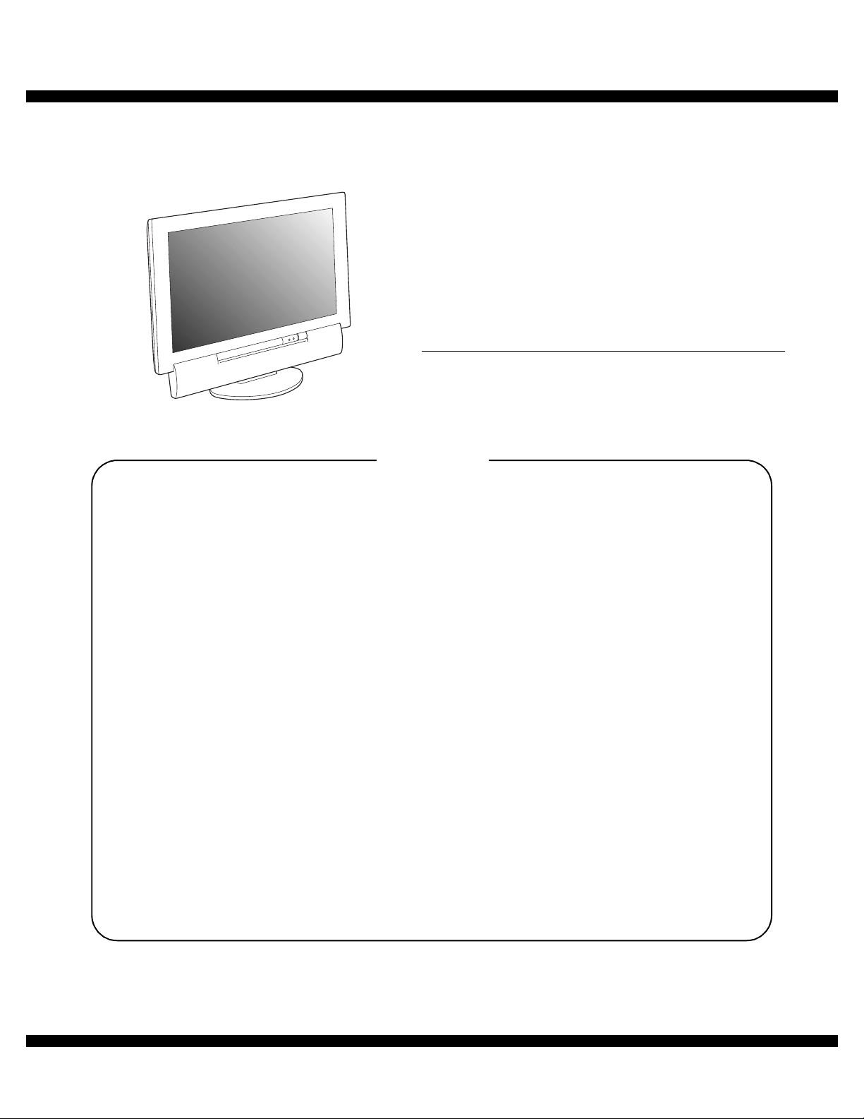
LCD COLOR TV
MODEL
CONTENTS
OUTLINE OF THE PRODUCT, NOMENCLATURE AND FUNCTION
. . . . . . . . . . . . . . . . . . . . . . . . . . . . . . . . . . . . . . . . . . . . . . .1 - 1
LD-26SH1U
CHAPTER 2. CONNECTION, ADJUSTMENT, OPERATION, AND FUNCTIONS
. . . . . . . . . . . . . . . . . . . . . . . . . . . . . . . . . . . . . . . . . . . . . . .2 - 1
CHAPTER 3. DISASSEMBLY AND ASSEMBLY . . . . . . . . . . . . . . . . . . . .3 - 1
CHAPTER 4. TROUBLE SHOOTING . . . . . . . . . . . . . . . . . . . . . . . . . . . .4 - 1
CHAPTER 5. BLOCK DIAGRAM . . . . . . . . . . . . . . . . . . . . . . . . . . . . . . . .5 - 1
CHAPTER 6. HARDWARE DESCRIPTION. . . . . . . . . . . . . . . . . . . . . . . .6 - 1
CHAPTER 7. CIRCUIT DIAGRAM & PWB LAYOUT. . . . . . . . . . . . . . . . .7 - 1
Parts marked with "!" are important for maintaining the safety of the set. Be sure to replace these parts with specified
ones for maintaining the safety and performance of the set.
SHARP CORPORATION
This document has been published to be used
for after sales service only.
The contents are subject to change without notice.
Page 2
CHAPTER 1. OUTLINE OF THE PRODUCT, NOMENCLATURE AND FUNCTION
1. SPECIFICATIONS
■ Product specifications
Model name LD-26SH1U
LCD display 26" Advanced Super-V and Anti-Glare
Actual display size 25.5" (64.8 cm) measured diagonally
Resolution (max.) 1366 x 768
Displayable colors
(max.)
Dot pitch (H x V) 0.4135 mm x 0.4135 mm
Brightness (max.) 500 cd/m
Contrast ratio 800:1
Angle of visibility Left-right 170°; up-down 170°
Screen display size (H x V)
Video signal Analog: Analog RGB (0.7 Vp-p) [75 Ω]
Sync signal Separate Sync (TTL level: +/-), Sync on
Video signal format NTSC
Expansion compensation
Plug & Play VESA DDC2B compatible
Power management VESA: based on DPMS
Speaker output 14 W in total
Input terminals Computer signal:
Output terminals Video image : RCA pin x 1
Receivable TV channels VHF : 2 through 13; UHF: 14 through 69;
Screen tilt Upward approx. 0° - 15°;
Screen swivel Approx. 90° from left through right
Power supply 100 VAC - 240 VAC, 50/60 Hz
Low-Reflection TFT LCD module
Approx. 16.77 million colors (8 bit)
2
(The screen brightness deteriorates over
time.Constant brightness cannot be maintained.)
s
(contrast ratio
564.8 mm x 317.6 mm (22.24" x 12.50")
Digital : DVI standard based on 1.0
Green, Composite Sync (TTL level: +/-)
Digital scaling (Enlarges VGA/SVGA/XGA
etc. to full screen size.)
[Enlarged display (full screen, fixed aspect
ratio)]
- 1:1 display is not possible.
DVI : based on DMPM
Analog: mini D-sub 15 pin (3 rows) x 1
Digital: DVI-D 24 pin x 1
(Also used for DVI image input terminal)
Computer audio: mini stereo jack (3.5mm) x 1
Video image: RCA pin x 3
Component image: x 1
S-video image: x 2
HDMI: x1
DVI-D 24 pin x 1
(Also used for computer digital signal input
terminal)
Audio: RCA pin (L/R x 3)
Antenna: F-type
S-video image: x 1
Audio : RCA pin (L/R x 1)
Headphone :
Cable: 1 through 125
downward approx. 0° - 5°
10)
(Available as an audio input
terminal for DVI mode)
mini stereo jack (φ3.5 mm) x 1
Temperature of operating environment
Power consumption 123 W*; 2.5 W in standby; 2.5 W in power-
Dimensions (W x D x H) Approx. 658 mm x 256 mm x 534 mm
Weight
5°C - 35°C (41°F - 95°F)
saving mode
When "BRIGHT MODE" is set to "BRIGHT".
*
80 W in "DARK1" and 67 W in "DARK2".
(Approx. 25.9" x 10.1" x 21.0")
Approx. 20.5 kg; 45.2 lb. (excluding signal
cable)
Approx. 16.5 kg; 36.4 lb. (excluding stand)
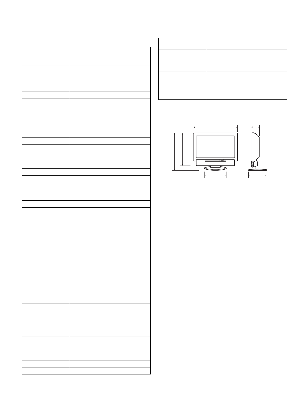
■ Dimensions (Units: mm)
658
534
487
324
• Power cord: approx. 1.8m (5.9ft.)
• PC analog signal cable: approx. 1.8m (5.9ft.)
• PC audio cable: approx. 1.8m (5.9ft.)
• Digital signal cable, NL-C04J (purchased separately): approx. 2.0 m (6.6 ft.)
Note: As a part of our policy of continuous improvement, SHARP
reserves the right to make design and specification changes for
product improvement without prior notice. The performance
specification figures indicated are nominal values of production
units. There may be some deviations from these values in individual units.
110
256
LD-26SH1U OUTLINE OF THE PRODUCT, NOMENCLATURE AND FUNCTION
1 – 1
Page 3
■ Relevant signal timings (PC mode)
Screen resolution Hsync Vsyn
VESA 640X480 31.5kHz 60Hz 25.175MHz
37.9kHz 72Hz 31.5MHz
37.5kHz 75Hz 31.5MHz
800X600 35.1kHz 56Hz 36.0MHz
37.9kHz 60Hz 40.0MHz
48.1kHz 72Hz 50.0MHz
46.9kHz 75Hz 49.5MHz
1024X768 48.4kHz 60Hz 65.0MHz
56.5kHz 70Hz 75.0MHz
60.0kHz 75Hz 78.75MHz
Wide 848X480 31.1kHz 60Hz 33.3MHz
1280X720 44.7kHz 60Hz 74.4MHz
1280X768 47.986kHz 60Hz 81.0MHz
60.15kHz 75Hz
1360X768 47.7kHz 60Hz 84.7MHz
US text 720X400 31.5kHz 70Hz 28.3MHz
Power
Macintosh
series
640X480 35.0kHz 66.7Hz 30.2MHz
832X624 49.7kHz 74.6Hz 57.3MHz
1024X768 60.2kHz 75Hz 80.0MHz
Dot
frequency
102.977MHz
Ana-
Digi-
log
tal
oo
oo
oo
-
o
oo
oo
oo
oo
oo
oo
-
o
-
o
oo
-
o
-
o
oo
o
-
o
-
o
-
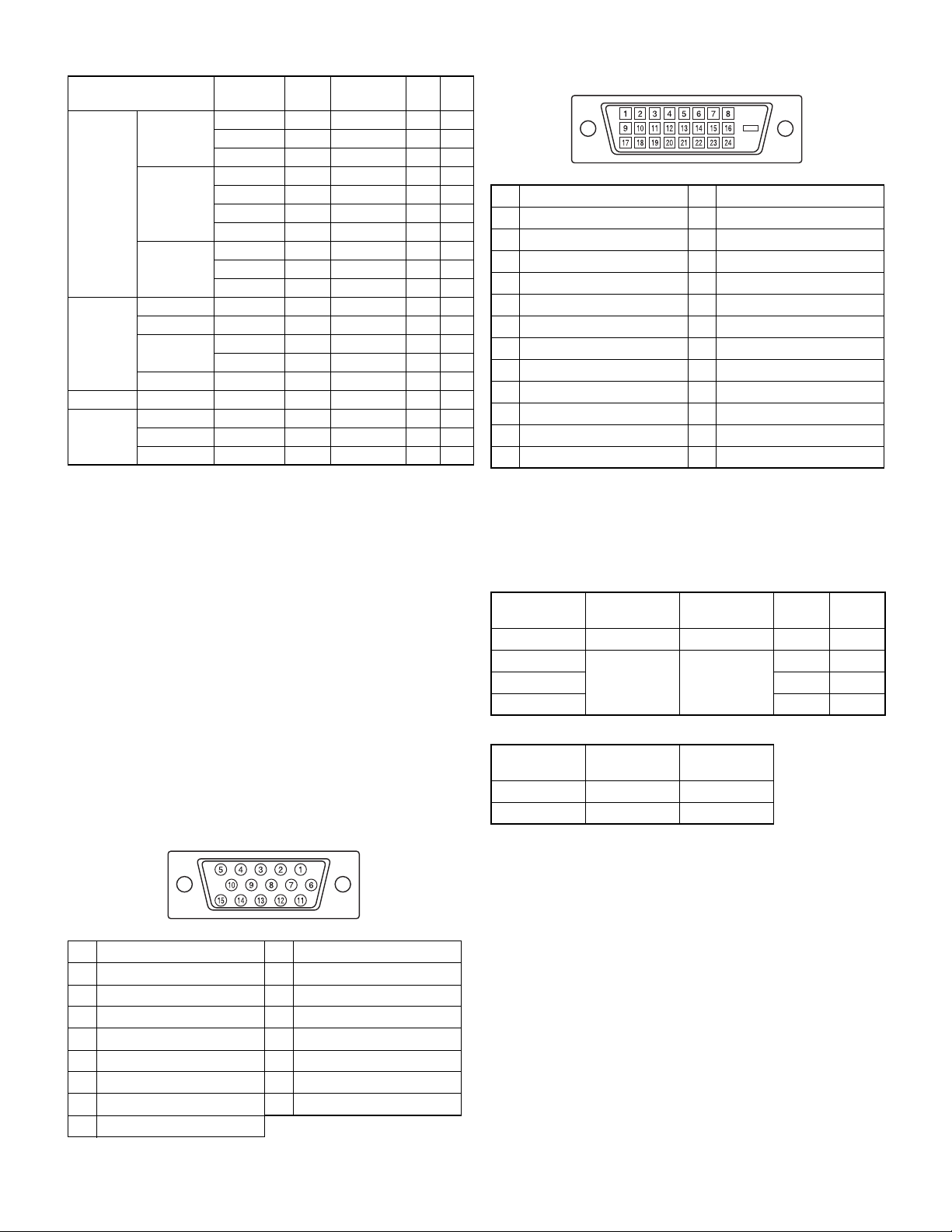
■ The analog RGB input connector pin
(DVI-D connector with 24 pins)
No. Function No. Function
1 TMDS data 2- 13 N.C.
2 TMDS data 2+ 14 +5V
3 TMDS data 2/4 shield 15 GND
4 N.C. 16 Hot plug detection
5 N.C. 17 TMDS data 0-
6 DDC clock 18 TMDS data 0+
7 DDC data 19 TMDS data 0/5 shield
8 N.C. 20 N.C.
9 TMDS data 1- 21 N.C.
10 TMDS data 1+ 22 TMDS clock shield
11 TMDS data 1/3 shield 23 TMDS clock +
12 N.C. 24
TMDS clock -
• Recommended resolution is 1360 x 768, 1280 x 768, or 1024 x 768.
• All are compliant only with non-interlaced.
• Depending on the type of computer to be connected, the display may
not work correctly even when the above relevant signals are input.
• Frequencies for Power Macintosh are reference values. To connect,
another adapter (commercially available) may be required.
• For digital connection, the TV can be connected to a computer with a
DVI-compatible output terminal (DVI-D 24 pin or DVI-I 29 pin).
(Depending on the type of computer to be connected, the display may
not work correctly.)
• If the TV is receiving timing signals that are not compatible, "OUT OF
TIMING" will appear. Follow your computer's operation manual to set
the timing so that it is compatible with the TV.
• If the TV is not receiving any signal (sync signal), "NO SIGNAL" will
appear. will appear.
■ The analog RGB input connector pin
(Mini D-sub connector with 15 pins)
No. Function No. Function
1 Red video signal input 9 +5V
2 Green video signal input 10 GND
3 Blue video signal input 11 N.C.
4 N.C. 12 DDC data
5 GND 13 For Hsync signal input
6 For red video signal GND 14 For Vsync signal input
7 For green video signal GND 15 DDC clock
8 For blue video signal GND
■ Power management
The monitor is based on the VESA DPMS and the DVI DMPM standards. To activate the power management function, the video card and
the computer used with it must also conform to these standard.
DPMS: Display Power Management Signaling
DPMS mode Screen
ON Display on 123 W Yes Yes
STANDBY
SUSPEND Yes No
OFF No No
DMPM: Digital Monitor Power Management
DPMS mode Screen
ON Display on 123 W
OFF Display off 2.5 W
Display off 2.5 W
Power
consumption
Power
consumption
H-sync V-sync
No Yes
■ DDC (Plug & Play)
This monitor supports the VESA DDC (Display Data Channel) standard.
DDC is a signal standard for carrying out Plug & Play functions on the
monitor or computer. It transfers information such as degree of resolution between the monitor and computer. You can use this function if
your computer is DDC compliant and if it is set so that it can detect the
Plug & Play monitor.
There are many varieties of DDC due to the differences between systems. This monitor works with DDC2B.
LD-26SH1U OUTLINE OF THE PRODUCT, NOMENCLATURE AND FUNCTION
1 – 2
Page 4
2. PRODUCT DESCRIPTION
Main unit
B
21
24
22
23
1
Opening/closing the front cover
To open the cover, press .
To close the cover, press until it clicks.
MENUINPUT
6
89
7
Speakers
1
Headphone terminal
2
Remote sensor window
3
POWERbutton
4
Power LED
5
11
12
13
14
2
15
3
4
16
5
17
18
19
BRIGHT
VOL /
CH
ENTER/
MODE
BRIGHT
10
20
Green : in use
Red : in standby mode
Orange : in power-saving mode (only for PC mode)
Off : power off
S-video input terminal
6
Video input terminal
7
Audio input terminal - Left
8
Audio input terminal - Right
9
Control buttons
F
Antenna input terminal
G
Video input terminal
H
Audio input terminal - Left
I
Audio input terminal - Right
J
S-video input terminal
K
Video input terminal
L
Audio input terminal - Left
M
Audio input terminal - Right
N
Component input terminals
O
S-video output terminal
P
Video output terminal
Q
Audio output terminal - Left
R
AV-IN3
AV-IN1
AV-IN2
(Available as an audio input
terminal for DVI mode)
Audio output terminal - Right
S
AV-OUT
(Available as an audio input
terminal for DVI mode)
HDMI input terminal
T
DVI input terminal
U
(DVI-D 24 pin)
(Available as a digital RGB input terminal for PC mode)
PC analog RGB input terminal (Mini D-sub 15 pin)
V
PC audio input terminal
W
Power input terminal
X
Lug-hole for cable clamp
Y
A Ventilation openings
B Exhaust openings Never block these openings as this may lead
to overheating inside the TV and result in
malfunction.
C Security lock anchor By connecting a security lock (commercially
available) to the security lock anchor, the TV
is fixed so that it cannot be transported. The
security slot works in conjunction with Kensington Micro Saver Security Systems.
A
26
25
27
28
Removing the cover
B
29
C
Replacing the cover
2
1
2
1
Be careful not to pinch the cables.
Remote control
POWER
1
2
3
4
BRIGH T
FREEZE
SLEEP
MODE
PC HDMI/ DVIAVTV
MULTI
5
6
DISPLA Y
7
8
POWER button
1
FREEZE button
2
SLEEP button
3
4 bc e d
5
6
7
8
9
F
G
H
I
J
K
L
M
N
O
buttons and ENTER button
BRIGHT MODE button
DISPLAY button
CC (Closed Caption) button
Channel buttons
Dolby Virtual button
Input buttons (PC, TV, AV, and HDMI/DVI)
VIEW MODE button
MULTI button
MENU button
BRIGHT button
MUTE button
MTS (Multi ch TV Sound) button
VOL buttons
CH (channel) buttons
FLASHBACK button
VIEW MOD E
MENU
ENT ER
CC MT S M U TE
FLASHBA CK
Vir t ual
BRIGHT
VO L
CH
9
10
11
12
13
14
15
16
17
18
19
LD-26SH1U OUTLINE OF THE PRODUCT, NOMENCLATURE AND FUNCTION
1 – 3
Page 5
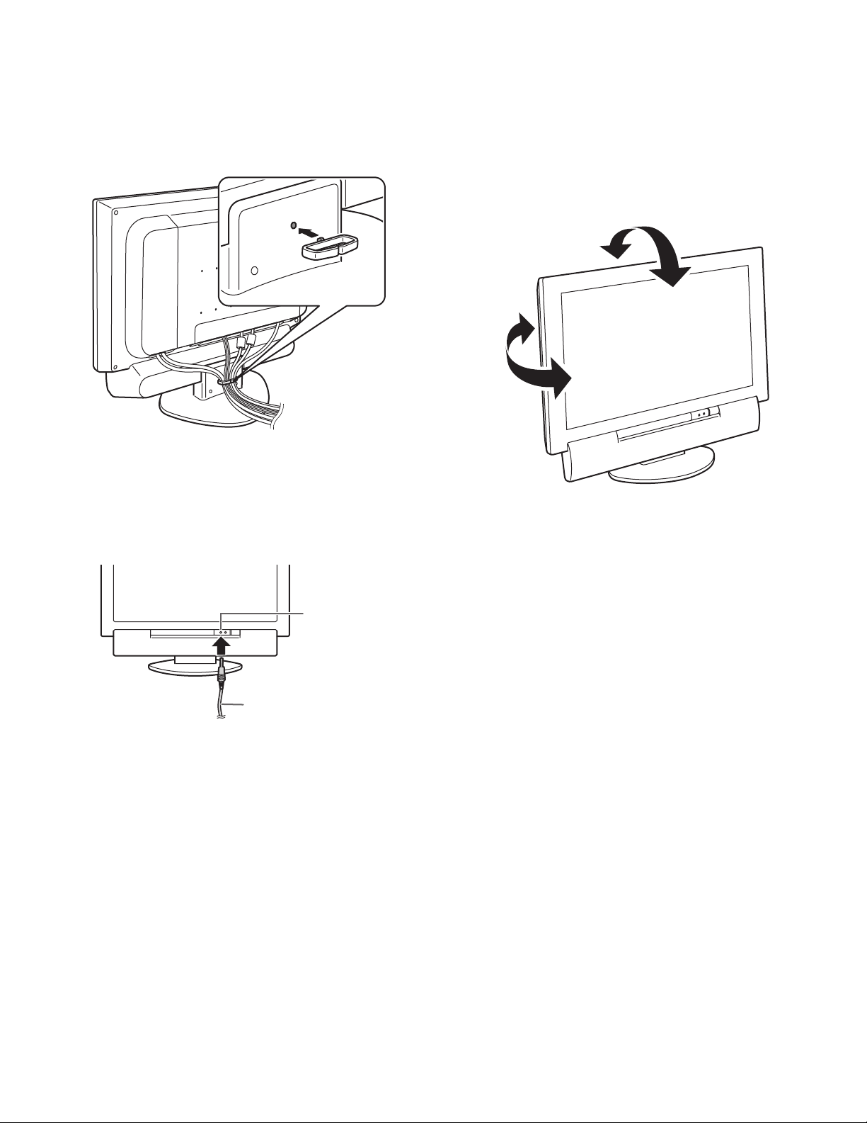
■ Cable clamp
Use the supplied cable clamp to secure the cables connected to the terminals.
Caution: When adjusting the viewing angle, cables may be pulled.
Therefore, ensure that the cables have sufficient slack.
■ Angle adjustment
Adjust to an easy to view angle.
Caution:
• Be sure to hold both sides of the TV when adjusting the viewing
angle. The LCD panel used in this TV is made of glass. Pressure
from hands on the LCD panel could cause damage.
• Be careful not to allow your fingers to be pinched.
approx. 15˚
■ Using headphones (commercially available)
You can connect headphones with a mini stereo jack (3.5 mm) to the
TV.
Headphone
terminal
Headphones
approx.
45˚
approx. 5˚
approx. 45˚
Note:
• When headphones are connected:
• No sound can be heard from the TV speakers. In addition, when
"AV-OUT(AUDIO)" is set to "VARIABLE1" or "VARIABLE2" in the
MODE SELECT(2) menu, no sound via the audio output terminals
can be heard either.
• The Virtual Dolby Surround function cannot be used.
• The AUDIO ADJUST menu cannot be adjusted.
LD-26SH1U OUTLINE OF THE PRODUCT, NOMENCLATURE AND FUNCTION
1 – 4
Page 6
CHAPTER 2. CONNECTION, ADJUSTMENT, OPERATION, AND FUNCTIONS
(
)
y
1. CONNECTION
1-1. Connecting the TV to a computer
Caution:
• When connecting, ensure that the TV and all the equipment you
are connecting to it are switched off.
• Be careful not to over bend the cable or add extension cords as this
could lead to a malfunction.
Notes:
• When using the TV with an analog connection, perform an automatic screen adjustment (page E31) under the following conditions:
- Using the TV for the first time.
- After having changed the system settings during use.
• When using the TV with a digital connection, automatic screen
adjustment is unnecessary.
• Depending on the computer or OS, you may have to install the setup information for the TV.
• When connecting to a notebook computer and the notebook computer's screen is set so that it is displaying at the same time, the
MS-DOS screen may not be able to display properly.
In this case, change the settings so that only the TV is displaying.
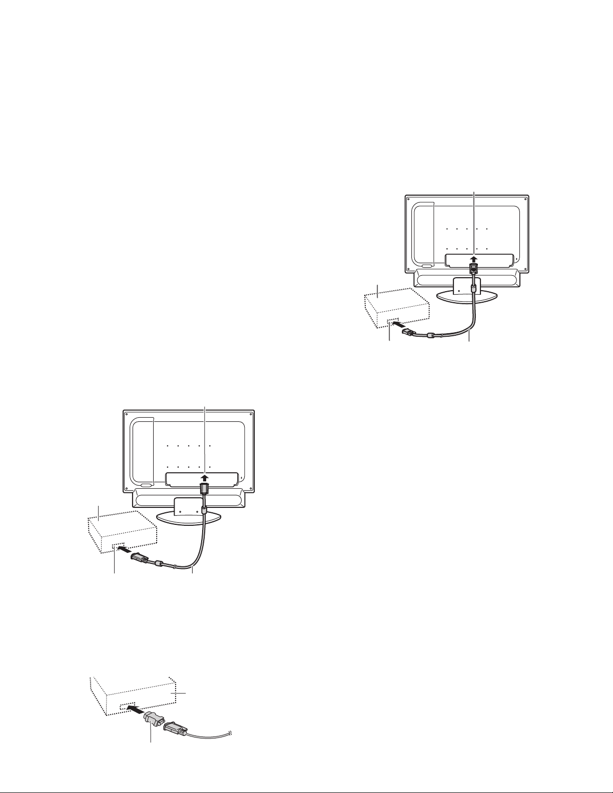
■ Analog connection
Connect the supplied PC analog signal cable to the analog RGB output
terminal of the computer.
For information on removing/replacing the terminal cover.
PC analog RGB input terminal
(Mini D-sub 15 pin, 3 rows)
Computer
Analog RGB output terminal
(Mini D-sub 15 pin, 3 rows)
• Paying attention to the connector direction, firmly insert the signal
cable straight into the connector, and then tighten the screws at both
ends.
If connecting to a D-sub 15 pin 2 row Apple Power Macintosh, attach a
Macintosh conversion adapter (commercially available) to the analog
signal cable.
PC analog signal cable
supplied
■ Digital connection
Connect the separately-sold digital signal cable (model name: NLC04J) to the digital RGB output terminal of the computer.
• The TV has an input terminal for connecting to a computer with a
DVI-compatible output terminal (DVI-D 24 pin or DVI-I 29 pin).
(Depending on the type of computer to be connected, the display may
not work correctly.)
DVI input terminal
(DVI-D 24 pin)
Computer
Digital RGB output
terminal
• Paying attention to the connector direction, firmly insert the signal
cable straight into the connector, and then tighten the screws at both
ends.
Notes:
• Make sure that the connected equipment is switched off.
• After making the connection, follow the procedure below.
1. Press [POWER] button to turn on the TV.
2. Press the PC button once or twice to select PC (digital) mode.
After a short time, the message asking you to change the "DVI
SELECT" setting might appear. When the message appears,
go to step 3.
3. Press the [
The computer will be selected as the connected equipment and
the message will disappear.
4. Turn on the computer.
• If the message described in step 2 appears during the operation,
follow the instructions in the message for the proper setting and
then turn off/on the power of the connected equipment.
]button to select "PC".
d
Digital signal cable
(separatel
-sold)
Power Macintosh
Macintosh conversion adapter
LD-26SH1U CONNECTION, ADJUSTMENT, OPERATION, AND FUNCTIONS
2 – 1
Page 7
■ Connecting the audio cable
Connect the supplied PC audio cable to the audio output terminal of the
computer.
Connect the supplied PC audio cable to the audio output terminal of the
computer.
PC audio input terminal
Audio
output
terminal
Computer
PC audio cable
(supplied)
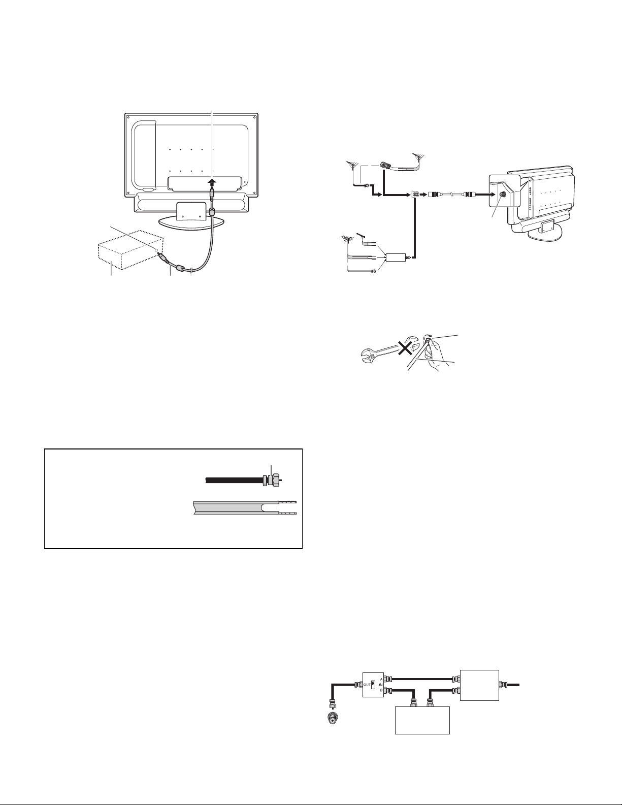
■ Outdoor antenna connection
• Use one of the following two diagrams if you connect an outdoor
antenna.
A : Using a VHF/UHF combination outdoor antenna.
B : Using separate VHF and/or UHF outdoor antennas.
• Connect the outdoor antenna cable lead-in to the antenna input terminal (ANT) on the left side of the TV.
A. Combination VHF/UHF Antenna
VHF/UHF
antenna
B. Separate VHF and/or
UHF Antennas
VHF
antenna
Caution: When connecting the coaxial cable to the TV, do not tighten F-
300/75-ohm
adapter
(commercially available)
75-ohm
coaxial cable
UHF
antenna
300-ohm
twin-lead
75-ohm
or
coaxial cable
or
300-ohm
twin-lead
Combiner
(commercially
available)
VHF/UHF
antenna
300-ohm
twin-lead
Home Antenna
terminal (75-ohm)
Antenna cable
(commercially available)
OUTIN
Antenna input terminal
(ANT)
type connector with tools. If tools are used, it may cause damage to your TV. (The breaking of internal circuit, etc.)
F-type connector
1-2. Connecting the TV to a home antenna terminal
Caution: When connecting, ensure that the TV is switched off.
The antenna requirements for good color television reception are more
important than those for black & white television reception. For this reason, a good quality outdoor antenna is strongly recommended.
The following is a brief explanation of the type of connections that are
provided with the various antenna systems.
1. A 75-ohm system is generally a
round cable with F-type connector
that can easily be attached to a terminal without tools (commercially
available).
75-ohm coaxial cable (round)
2. A 300-ohm system is a flat "twinlead" cable that can be attached to a
75-ohm terminal through a 300-75-
300-ohm twin-lead cable (flat)
ohm adapter (commercially available).
Notes:
• The 75-ohm coaxial cable is recommended.
• TV memory for channels is empty at shipment.
To receive channels, use the CHANNEL SETTING menu.
F-type connector
75-ohm coaxial cable
■ Cable TV (CATV) connection
• A 75-ohm coaxial cable connector is built into the set for easy hookup.
When connecting the 75-ohm coaxial cable to the set, screw the 75ohm cable to the antenna input terminal (ANT).
• Some cable TV companies offer "premium pay channels". Since the
signals of these premium pay channels are scrambled, a cable TV
converter/descrambler is generally provided to the subscriber by the
cable TV company. This converter/descrambler is necessary for normal viewing of the scrambled channels. (Set your TV to channel 3 or
4, typically one of these channels is used. If this is unknown, consult
your cable TV company.) For more specific instructions on installing
cable TV, consult your cable TV company. One possible method of
utilizing the converter/descrambler provided by your cable TV company is explained below.
Please not :An RF switch provided with two inputs (A and B) is
required (commercially available).
"A" position on the RF switch (commercially available):
You can view all unscrambled channels by using the TV's channel
buttons.
"B" position on the RF switch (commercially available):
You can view the scrambled channels via the converter/descrambler
by using the converter's channel keys.
RF switch (commercially available)
OUT
Cable TV converter/
descrambler
(commercially
available)
IN
Two-set
signal
splitter
(commercially
available)
Cable TV Line
Note: Consult your SHARP Dealer or Service Center for the type of
splitter, RF switch, or combiner that might be required.
LD-26SH1U CONNECTION, ADJUSTMENT, OPERATION, AND FUNCTIONS
2 – 2
Page 8
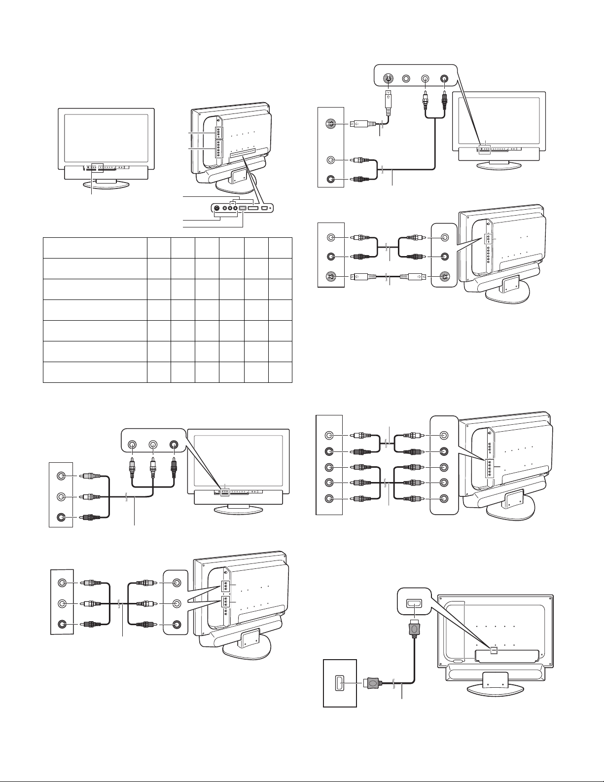
1-3. Connecting the TV to AV equipment
Caution: Ensure that the TV and all the equipment you are connecting
to it are switched off before you begin.
■ Examples of equipment you can connect
Front of the TV Right side of the TV
■ Connecting the TV to AV equipment
AV equipment with S-video output terminals
S-VIDEO
VIDEO
AUDIO-L AUDIO-R
Output terminals of
AV equipment
S-VIDEO
(White) (Red)
Front of the TV
AV-IN1
AV-IN2
AV-IN 3
DVI-D IN
AV-OU T
HDMI IN
AV-
AV-
AVIN 3
HDM
I IN
AV equipment with
video output terminals
AV equipment with
S-video output terminals
AV equipment with
component output terminals
AV equipment with
HDMI output terminals
AV equipment with
DVI output terminals
AV equipment with
input terminals
IN 1
IN 2
ooo---
o - o ---
- o ----
---o --
----o -
-----o
■ AV equipment with video output terminals
Connecting the TV to AV equipment
Front of the TV
VIDEO
AUDIO-L AUDIO-R
Output terminals of
AV equipment
VIDEO
AUDIO-L
(Yellow)
(White)
(Yellow)
(White)
(Red)
AV-IN 3
DVID IN
AV-
OUT
S-video cable (commercially available)
AUDIO-L
AUDIO-R
Output terminals of
AV equipment
AUDIO-L
AUDIO-R
S-VIDEO
(White)
(Red)
(White)
(Red)
RCA pin cable (commercially available)
S-videocable (commercially available)
RCA pin cable (commercially available)
AUDIO-L
(White)
AUDIO-R
(Red)
S-VIDEO
AV-IN 3
Right side of the TV
AV-IN 1
Note: When using the S-video input terminal of AV-IN 1 or AV-IN 3, do
not connect the cable to the video input terminal of the same
group.
■ AV equipment with component output terminals
Connecting the TV to AV equipment
Output terminals of
AV equipment
AUDIO-L
AUDIO-R
RCA pin cable
(commercially available)
(White) (White)
(Red) (Red)
Y
(Green) (Green)
b
P
(Blue) (Blue)
P
r
(Red) (Red)
AUDIO-L
AUDIO-R
P
P
Y
b
r
Right side of the TV
AV-IN 2
AUDIO-R
(Red)
RCA pin cable (commercially available)
Right side of the TV
Output terminals of
AV equipment
VIDEO
(Yellow)
(Yellow)
VIDEO
AV-IN 1
AUDIO-L
AUDIO-R
(White)
(Red)
(White)
(Red)
AUDIO-L
AUDIO-R
AV-IN 2
RCA pin cable (commercially available)
Notes: • When using the video input terminal of AV-IN 1 or AV-IN 3,
do not connect the cable to the S-video input terminal of the
same group.
• When using the video input terminal of AV-IN 2, do not connect the cable to the component input terminals of AV-IN 2.
LD-26SH1U CONNECTION, ADJUSTMENT, OPERATION, AND FUNCTIONS
Component video cable
(commercially available)
Note: When using the component input terminals, do not connect the
cable to the video input terminal of AV-IN 2.
AV equipment with HDMI output terminals
Rear of the TV
HDMI IN
Output terminals of
AV equipment
HDMI
HDMI cable (commercially available)
Note: If necessary, you can make adjustments for HDMI setup using
the HDMI SETUP menu (HDMI mode).
2 – 3
Page 9
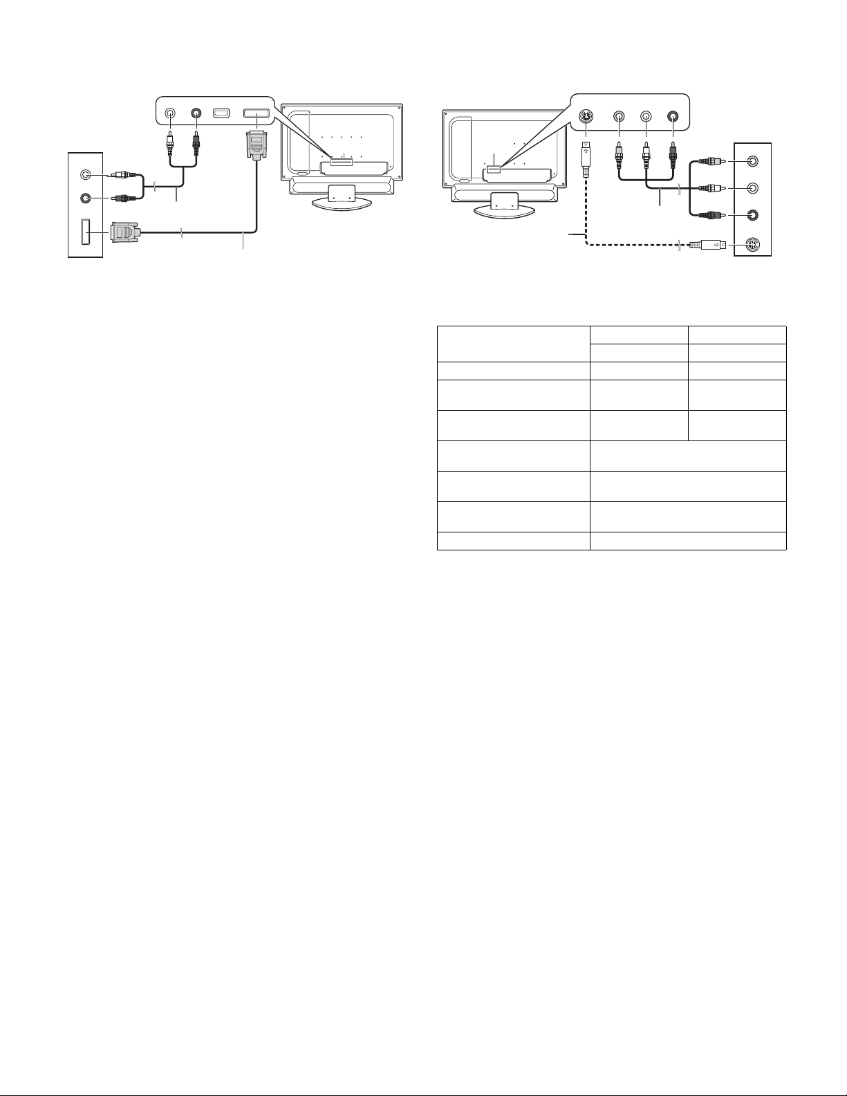
■ AV equipment with DVI output terminals
Connecting the TV to AV equipment
Re ar o f t h e TV
DVI-D IN
Output terminals of
AV equipment
AUDIO-L
AUDIO-R
(Whit e)
(Red)
DIGIT AL
AUDIO- L AUDIO- R
(Whit e) (Red)
RCA pin cabl e
(commercially available)
HDMI DIGI TAL
Digital signal cable
(separ at el y sol d , NL- C04J)
Notes: • Make sure that the connected equipment is switched off.
• Use the audio output terminals of AV-OUT as the audio
input terminals for DVI.
• After making the connection, follow the procedure below.
1. Press [POWER] button to turn on the TV.
2. Press the [HDMI/DVI] button once or twice to select DVI
mode.
If the message asking you to change the "DVI SELECT"
setting appears, press the button to select "AV". Go to
step 3 after the message disappears.
3. Press the [MENU] button to display the MENU screen.
4. Select the MODE SELECT menu.
5. Be sure to set "DVI SELECT" to "AV". (The factory setting
is "AV".)
6. Be sure to set "AV-OUT(AUDIO)" to "DVI AUDIO-IN".
(The factory setting is "DVI AUDIO-IN".)
7. Press the [MENU] button to exit the screen.
8. Turn on power for the connected equipment.
• If the message described in step 2 appears during the operation, follow the instructions in the message for the proper
setting and then turn off/on the power of the connected
equipment.
■ AV equipment with input terminals
Connecting the TV to AV equipment
Re a r o f t h e TV
AV- OU T
S- v i d e o c a b l e
(commercially available)
The image displayed on the TV screen and the sound can be output via
the AV-OUT terminals to AV equipment.
The AV-OUT terminal used to output the image differs depending on
the terminal used for the input.
Image displayed on the TV
TV image
Image input from the video
input terminal
Image input from the Svideo input terminal
Image input from the component input terminals
Image input from the DVI
input terminal
Image input from the HDMI
input terminal
Computer Image
1 Only the sound is output.
*
2 Only the sound set as "SOUND" using the MODE SELECT1 menu
*
is output.
While displaying the PIP/SPLIT window:
• The image displayed in the PIP/SPLIT window is output. However, the image input from the component input terminals or
HDMI input terminal cannot be output even if it is displayed in the
PIP/SPLIT window.
• The sound set as "SOUND" using the MULTI SCREEN menu is output.
Notes:
• Select the item you want to set in "AV-OUT(AUDIO)" using the MODE
SELECT (2) menu, according to your requirements.
• DVI AUDIO-IN ...Use when connecting to AV equipment with DVI
• FIXED .............. Use when connecting to a VCR for recording,
• VARIABLE1 ...... Use to enjoy the sound from both the TV speak-
• VARIABLE2 ...... Use to enjoy only the sound from the external
S- VI D EO V I D EO
AUDIO- L AUDIO- R
(Yellow) (White)
RCA pin cable
(commercially avai labl e)
(Red)
Input terminals of
AV equipment
(Yellow )
AUDIO- L
(Whit e)
(Red)
AUDIO- R
S- VI D EO
VIDEO
Output from
Video terminal S-video terminal
ou
ou
oo
1
*
u
u
u
2
*
u
output terminals. This setting enables the audio
output terminals to act as the audio input terminals for DVI mode.
etc. The volume of the sound via the audio output terminals is fixed.
ers and external speakers while watching the
image on the TV, etc. [VOL +/-] buttons allow
you to adjust the sound volume for both the TV
and external speakers.
speakers while watching the image on the TV,
etc. No sound can be heard from the TV speakers with this setting.
[VOL +/-] buttons allow you to adjust the sound
volume for the external speakers.
LD-26SH1U CONNECTION, ADJUSTMENT, OPERATION, AND FUNCTIONS
2 – 4
Page 10
1-4. Connecting the TV to a power source
Caution:
• When connecting, ensure that the TV is switched off.
• Use only the power cord supplied with the TV.
• Be careful not to over bend the cable or add extension cords as this
could lead to a malfunction.
1. Connect the power cord (supplied) to the power input terminal.
Power input terminal
2. Spread out a soft cloth on a flat surface. Being careful not to damage
the TV, gently lay the TV on it display-side down.
3. Remove the two screws and then remove the rear cover of the stand.
AC adapter (supplied)
2. Place the power plug into an AC outlet.
AC outlet
Power cord (supplied)
Note: If the TV does not operate, disconnect the power cord from the
AC outlet and reconnect it again. The setup must be completed
in the proper order for the TV to function.
1-5. Instructions for attaching a VESA-compliant mount
An arm or stand based on the VESA standard (commercially available)
can be attached to the TV.
Procurement of the arm or stand is at the customer's discretion.
4. Remove the six screws and then remove the stand from the TV.
Notes:
• The stand is specially made for use with this TV. Once having
removed the stand, never attempt to attach it to another equipment.
• Once having removed the screws, store them together with
the stand. If the stand is ever re-attached, be sure to use the
original screws.
Using different screws could lead to a malfunction.
5. Attach the arm to the TV with the six screws.
■ Arms or stands able to be used
Attachments must satisfy the following.
• Compatible with the VESA standard.
• The six screw holes on the section to be attached have a gap of 100
mm between them.
• Not be likely to fall off or break off after being attached to the TV.
■ How to attach the arm or stand
• Be careful not to over bend the cable or add extension cords as this
could lead to a malfunction.
• While following these instructions, please also refer to the installation
instructions in the operation manual included with the arm or stand.
Caution:
1. Remove the terminal covers and the cables.
• Be careful not to get your fingers pinched between the display and stand nor to let the stand drop. These could lead
to injury.
• Do not cover or block the vents and openings since insufficient ventilation can cause overheating.
LD-26SH1U CONNECTION, ADJUSTMENT, OPERATION, AND FUNCTIONS
Note: The screws used to attach the arm should be M4 screws with a
length of 12 mm - 14 mm (0.47" -0.55") protruding from the surface to be attached.
Using different screws could cause the TV to fall off or to be
internally damaged.
12 mm - 14 mm (0.47" - 0.55")
Screw used to attach arm
Arm
Part of TV to which arm is attached
6. Reconnect the cables and replace the terminal covers.
2 – 5
Page 11
2. ADJUSTMENT
T
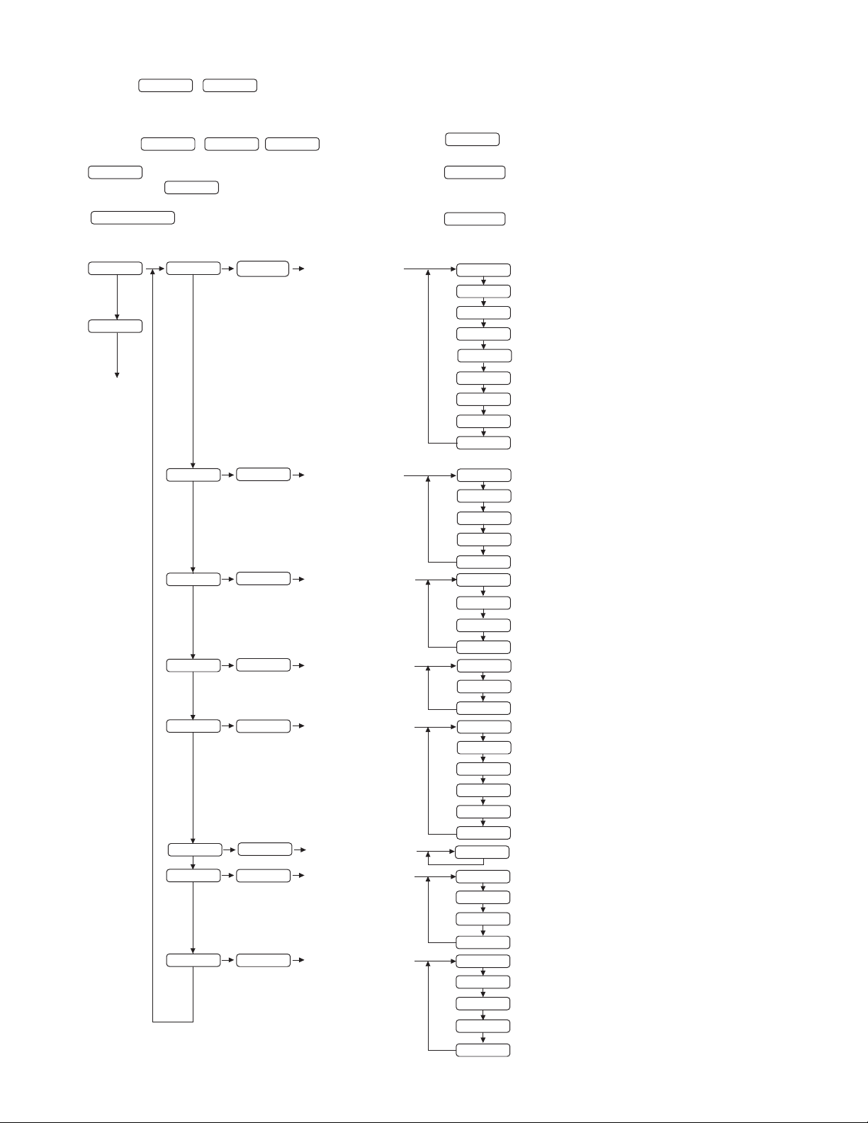
2-1. ADJUSTMENT METHOD (PC MODE)
* Press the PC button to select PC mode.
1) Resetting all adjustment values
Press the
MENU , , POWER buttons.
ENTER/BRIGHT
2) Adjustment lock function
MENU
+ Power ON
(And press the button. )
d
3) DOLBY VIRTUAL
DOLBY VIRTUAL
ON/OFF
4) VIEW MODE
VIEW MODE
MULTI SCREEN DISPLAY
5)
MULTI
PIP POSITION
6)
CHANGE
CHANGE
While displaying the PIP window, you can also set this item directly using
the bc de buttons, instead of the adjustment screen.
7)
Adjustment pattern
MENU
MENU
END
c
c
ENTER
ENTER
ADJUSTMENT
(Analog)
GAIN
CONTROL
ENTER
ENTER
(Analog)
c
ENTER
AUDIO
ADJUST
*
If you do not press any buttons for about 30 seconds
while in a menu screen, the settings you made up to
that point will be applied and the screen will
automatically disappear.
AUTO
CLOCK
PHASE
H-POS
V-POS
RESET
AUTO
BLACK LEVEL
CONTRAST
RESET
TREBLE
BASS
BALANCE
DOLBY VIRTUAL
(e d buttons)
(e d buttons)
(e d buttons)
(e d buttons)
(e d buttons)
(e d buttons)
(e d buttons)
(e d buttons)
(e d buttons)
(e d buttons)
c
c
c
ENTER
ENTER
ENTER
COLOR
CONTROL
MODE
SELECT-1
MODE
SELECT-2
COLOR CONTROL
WHITE BALANCE
RESET
VIEW MODE
480 LINES
768 LINES
SOUND
SCALING
LANGUAGE
RESET
QUICK SHOOT
AV-OUT (AUDIO)
DVI SELECT
(e d buttons)
(e d buttons)
(e d buttons)
(e d buttons)
(e d buttons)
(e d buttons)
(e d buttons)
(e d buttons)
(e d buttons)
(e d buttons)
(e d buttons)
(COOL2, COOL1, STD,
WARM1, WARM2, USER)
c
c
c
R-CONTRAST
(e d buttons)
G-CONTRAS
(e d buttons)
B-CONTRAST
(e d buttons)
RESET
c
ENTER
MULTI
SCREEN
MULTI SCREEN DISPLAY
PIP SIZE
PIP POSITION
PC POSITION
SUB SOURCE
SOUND
(e d buttons)
(e d buttons)
(e d buttons)
(e d buttons)
(e d buttons)
(e d buttons)
RESET
LD-26SH1U CONNECTION, ADJUSTMENT, OPERATION, AND FUNCTIONS
2 – 6
Page 12
2-2. ADJUSTMENT ITEM LIST (PC MODE)
BUTTON ITEM ADJUSTMENT DESCRIPTION
MENU MENU 1:
ADJUSTMENT
MENU 2:
GAIN CONTROL
MENU 3:
AUDIO ADJUST
MENU 4:
WHITE BALANCE
MENU 5:
MODE SELECT-1
MANUAL CLOCK 0~255 CLOCK: Adjust so that vertical flicker noise is not emitted.
PHASE 0~255 PHASE: Adjust so that horizontal flicker noise is not emitted.
H-POS Indefinite H-POS (horizontal positioning) and V-POS (vertical positioning)
V-POS Indefinite
AUTO Automatic screen adjustment
MANUAL BLACK LEVEL 0~100 BLACK LEVEL: Total screen brightness can be adjusted
CONTRAST 0~100 CONTRAST: While watching the color pattern, adjustments can be
AUTO GAIN CONTROL Menu
TREBLE -30~0~+30 Adjusts high-pitch sounds.
BASS -30~0~+30 Adjusts low-pitch sounds.
BALANCE -30~0~+30 Adjusts the balance between the right and left speakers.
DOLBY VIRTUAL ON/OFF Turns the Virtual Dolby Surround function "ON" or "OFF".
COLOR MODE STD, sRGB,
WHITE BALANCE COOL2, COOL1,
VIEW MODE NORMAL, FULL Selects the screen size.
480 LINES 640, 848
768 LINES 1024, 1280, 1360
SOUND
SCALING 1~4
LANGUAGE
VIVID
STD, WARM1,
WARM2
USER R, G, B:
0~255
PC, TV, AV1, AV2,
AV3
AUTO: Every menu option is automatically adjusted using the
You can also set this item directly using the remote control, instead
of the adjustment screen.
Selects the color tone.
WHITE BALANCE Menu
USER
NORMAL :
FULL :
Specifies the horizontal resolution of a 480-line screen. (For analog signals)
640 : 640 x 480 dot mode
848 : 848 x 480 dot mode
Specifies the horizontal resolution of a 768-line screen. (For analog signals)
1024 : 1024 x 768 dot mode
1280 : 1280 x 768 dot mode
1360 : 1360 x 768 dot mode
Selects the audio to listen to while displaying the computer screen.
When the PIP/SPLIT window is displayed, the audio set by "SOUND" in the
MULTI SCREEN menu takes precedence.
When "STATUS" in the V-CHIP BLOCK menu is "ON",
TV/AV-IN SOUND is not available in PC mode.
Adjusts the image to optimum sharpness when it is enlarged.
Selects the language (English, French or Spanish) on the screen.
(
buttons)
e d
(
buttons)
e d
To center the screen image within the boundaries of the screen,
adjust the left-right (H-POS) values and the up-down (V-POS) values. (
Options in the ADJUSTMENT Menu can be adjusted automatically
(CLOCK, PHASE, H-POS V-POS).
COOL2 : Color tone bluer than standard
COOL1 : Color tone slightly bluer than standard
STD : Color tone standard setting
WARM1: Color tone slightly redder than standard
WARM2: Color tone redder than standard
buttons)
e d
while watching the color pattern. (
made so that all graduations appear. (
Auto Gain Control function.
STD : Displays images using the original color tone of the LCD
sRGB : sRGB is an international standard for color rep
VIVID : Displays images in vivid primary colors.
R-CONTRAST:
G-CONTRAST:
B-CONTRAST:
monitor.
resentation defined by the IEC
International Electrotechnical Commission).
Colors are converted by taking into account the
liquid crystal's characteristics and thereby
represent color tone close to the original image.
button for blue-green, d button for red
e
button for purple, d button for green
e
button for yellow, d button for blue
e
Displays the image without changing its aspect ratio. When
the image's resolution is lower than 1024 x 768, the image is
expanded.
Expands the image so that it fills the screen.
(The aspect ratio may change.)
You can also set this item directly using the remote control,
instead of the adjustment screen.
e d
buttons)
buttons)
e d
LD-26SH1U CONNECTION, ADJUSTMENT, OPERATION, AND FUNCTIONS
2 – 7
Page 13
BUTTON ITEM ADJUSTMENT DESCRIPTION
QS :
MENU
MENU 6:
MODE SELECT-2
QUICK SHOOT ON/OFF
AV-OUT (AUDIO) DVI AUDIO-IN,
DVI SELECT AV, PC Set depending on equipment connected to the DVI input terminal.
FIXED,
VARIABLE1,
VARIABLE2
QUICK SHOOT
Reduces the visual lag inherent in fast-motion scenes.
Selects how to adjust the sound via the audio output terminals.
• DVI AUDIO-IN : Enables these terminals to act as the audio input
• FIXED : : Set "FIXED" when connecting to a VCR for
• VARIABLE1 :Set to enjoy the sound from both the TV speak-
• VARIABLE2 :
terminals for DVI mode.
recording, etc.The volume is fixed.
Image and sound are simultaneously output via
the output terminals. (Image and sound are output via the output terminals a little earlier than
when image is displayed on the TV and sound is
output from the TV speakers.)
ers and external speakers while watching the
image on the TV, etc.
The volume can be adjusted.
Image is displayed on the TV at the same time
as when sound is output via the output terminals. (Sound is output via the output terminals a
little later than when image is output via the output terminal.)
Set to enjoy only the sound from the external speakers while watching the image on the TV, etc.
The volume can be adjusted.
However, no sound can be heard from the TV
speakers with this setting. (Sound can be output
via the headphone terminal.)
Image is displayed on the TV at the same time
as when sound is output via the output terminals. (Sound is output via the output terminals a
little later than when image is output via the output terminal.)
• A V : AV equipment
• P C : Computer
Be sure to turn off/on the power of the connected equipment after
you change the setting.
MENU 7:
MULTI SCREEN
MULTI SCREEN
DISPLAY
OFF, PIP, SPLIT Designates whether the computer's screen and TV or video images
are displayed simultaneously.
OFF:
PIP: The TV or video image appears in a small window
(PIP window) on the computer screen.
SPLIT: The computer's screen and the TV or video image appear
side by side in two split windows.
You can also set this item directly using the remote control,
instead of the adjustment screen.
PIP SIZE Changes the size of the PIP window.
PIP POSITION Adjusts the position of the PIP window.
] [c] buttons.
To move up and down, press the [
To move left and right, press the [
b
] [d] buttons.
e
While displaying the PIP window, you can also set this item directly
using the remote control, instead of the adjustment screen.
PC POSITION CENTER, LEFT Designates the position of the computer screen when the PIP win-
dow is displayed.
This item is enabled when the computer's "VIEW MODE" is set to
"NORMAL".
SUB SOURCE T V, A V 1 , A V 2 ,
Selects the video source of the PIP/SPLIT window.
AV3, HDMI
SOUND Selects the audio you want to hear while displaying the PIP/SPLIT
window.
• PC : Computer audio
• SUB SOURCE : TV or video audio
LD-26SH1U CONNECTION, ADJUSTMENT, OPERATION, AND FUNCTIONS
2 – 8
Page 14
2-3. ADJUSTMENT METHOD (TV/AV MODE)
Press the
* /
*
If you do not press any buttons for about 30 seconds while in a menu screen, the settings you made up to
TV
HDMI/DVI
that point will be applied and the screen will automatically disappear.
1) Resetting all adjustment values
Press the
MENU
ENTER/BRIGHT
,
2) Adjustment lock function
MENU
(And press the button.)
+ Power ON
d
3) DOLBY VIRTUAL
DOLBY VIRTUAL
7)
Adjustment pattern
MENU
MENU
END
ON/OFF
c
(HDMI, DVI) button to select TV or HDMI, DVI mode.
4) VIEW MODE
,
POWER
buttons.
VIEW MODE
5) SLEEP TIMER
SLEEP TIMER
(The time changes in the following order each time you press the button)
6) CC/TEXT
CC/TEXT
(The setting changes in the following order:)
ENTER
VIDEO ADJUST
CHANGE
to change the setting.
to change the setting.
c
CONTRAST
c
BLACK LEVEL
c
COLOR
c
TINT
c
SHARPNESS
c
FLESH TONE
c
VIDEO SELECT
c
WHITE BALANCE
c
RESET
(e d buttons)
(e d buttons)
(e d buttons)
(e d buttons)
(e d buttons)
(e d buttons)
(e d buttons)
(e d buttons)
c
c
c
c
c
c
c
ENTER
ENTER
ENTER
ENTER
ENTER
ENTER
ENTER
AUDIO ADJUST
CHANNEL SETTING
(TV mode only)
SCREEN ADJUST
MODE SELECT
CLOSED CAPTION
V-CHIP BLOCK
HDMI SETUP
c
c
c
c
c
c
c
c
c
c
c
c
c
c
c
c
c
c
c
c
c
c
c
c
c
c
c
c
TREBLE
BASS
BALANCE
DOLBY VIRTUAL
RESET
AIR/CABLE
CABLE MODE
CHANNEL SEARCH
CHANNEL MEMORY
VIEW MODE
POSITION
RESET
SLEEP TIMER
LANGUAGE
QUICK SHOOT
AV-OUT (AUDIO)
DVI SELECT
RESET
CC/TEXT
MPAA
TV GUIDELINES
STATUS
RESET
SIGNAL TYPE
COLOR MATRIX
DYNAMIC RANGE
AUTO VIEW
RESET
(e d buttons)
(e d buttons)
(e d buttons)
(e d buttons)
(e d buttons)
(e d buttons)
(e d buttons)
(e d buttons)
(e d buttons)
(e d buttons)
(e d buttons)
(e d buttons)
(e d buttons)
(e d buttons)
(e d buttons)
(e d buttons)
(e d buttons)
(e d buttons)
(e d buttons)
(e d buttons)
(e d buttons)
(e d buttons)
(e d buttons)
LD-26SH1U CONNECTION, ADJUSTMENT, OPERATION, AND FUNCTIONS
2 – 9
Page 15
2-4. ADJUSTMENT ITEM LIST (TV/AV MODE)
BUTTON ITEM ADJUSTMENT DESCRIPTION
MENU MENU 1:
VIDEO
ADJUSTMENT
MENU 2:
AUDIO ADJUST
MENU 3:
CHANNEL
SETTING
(TV mode only)
MENU 4:
SCREEN ADJUST
MENU 5:
MODE SELECT
CONTRAST
0~63
Adjusts contrast.
BLACK LEVEL 0~100 Adjusts the overall brightness of the screen.
COLOR -60~+60 Adjusts the color depth.
TINT -20~+20 Adjusts the color tone.
SHARPNESS 1~5 Adjusts the image quality.
FLESH TONE 1~5 Adjusts the flesh tone color.
VIDEO SELECT S T D ,
MOTION,
STILL
Selects the type of image to display improving the quality of the
images.
This adjustment is invalid for images from the S-video and component
input terminals.
WHITE BALANCE STD, WARM Adjusts the color temperature.
STD : Standard setting for color tone.
WARM : Color tone redder than standard.
TREBLE
BASS
BALANCE
DOLBY VIRTUAL
-30~0~+30 Adjusts high-pitch sounds.
-30~0~+30 Adjusts low-pitch sounds.
-30~0~+30 Adjusts the balance between the right and left speakers.
ON/OFF Turns the Virtual Dolby Surround function "ON" or "OFF".
You can also set this item directly using the remote control,
instead of the adjustment screen.
AIR/CABLE
CABLE MODE
CHANNEL SEARCH
CHANNEL MEMORY
VIEW MODE
-10~0~+10 Selects the screen size.
Sets the receiving mode broadcast (AIR) or cable TV (CABLE).
Set this item when "AIR/CABLE" is set to "CABLE".
Sets available channels automatically.
Sets channels manually.
NORMALDisplays 4:3 aspect ratio TV images normally.
WIDE : Expands 4:3 images horizontally to fill the entire screen
(16:9).
ZOOM1: Expands the image to fill the screen (16:9) with wide
black bands across the top and bottom such as letterbox format movies.
ZOOM2: Can be used when "ZOOM1" cuts off captions or telops at
the top or bottom of the screen.
FULL : Returns images horizontally reduced from 16:9 to 4:3
back to 16:9 so they fill the entire screen.
You can also set this item directly using the remote control, instead of
the adjustment screen.
Depending on the type of data received or the video software used,
screen edges may be slightly cut off or the image may have a black
border.
POSITION
-10~0~+10 Adjusts the position of the image.
V-POSITION : Adjusts the image's vertical position.
H-POSITION : Adjusts the image's horizontal position.
RESET : Resets the image's position to the monitor's original
factory setting.
SLEEP TIMER
Specifies how many minutes until the monitor switches off
(standby).
You can also set this item directly using the remote control, instead
of the adjustment screen.
LANGUAGE
QUICK SHOOT ON, OFF
Selects the language (English, Spanish, or French) on the screen.
QS :
QUICK SHOOT
Reduces the visual lag inherent in fast-motion scenes.
LD-26SH1U CONNECTION, ADJUSTMENT, OPERATION, AND FUNCTIONS
2 – 10
Page 16
BUTTON ITEM ADJUSTMENT DESCRIPTION
MENU
MENU 5:
MODE SELECT
MENU 6:
AV-OUT (AUDIO) Selects how to adjust the sound via the audio output terminals.
• DVI AUDIO-IN : Enables these terminals to act as the audio
input terminals for DVI mode.
• FIXED : : Set "FIXED" when connecting to a VCR for
recording, etc.The volume is fixed.
Image and sound are simultaneously output
via the output terminals. (Image and sound are
output via the output terminals a little earlier
than when image is displayed on the TV and
sound is output from the TV speakers.)
• VARIABLE1 : Set to enjoy the sound from both the TV
speakers and external speakers while watching the image on the TV, etc.
The volume can be adjusted.
Image is displayed on the TV at the same
time as when sound is output via the output
terminals. (Sound is output via the output terminals a little later than when image is output
via the output terminal.)
• VARIABLE2 : Set to enjoy only the sound from the external
speakers while watching the image on the
TV, etc.
The volume can be adjusted.
However, no sound can be heard from the
TV speakers with this setting. (Sound can be
output via the headphone terminal.)
Image is displayed on the TV at the same
time as when sound is output via the output
terminals. (Sound is output via the output terminals a little later than when image is output
via the output terminal.)
DVI SELECT Set depending on equipment connected to the DVI input terminal.
• A V : AV equipment
• P C : Computer
Be sure to turn off/on the power of the connected equipment after
you change the setting.
CC/TEXT Sets the CC/TEXT mode.
CLOSED CAPTION
MENU 7:
V-CHIP BLOCK
MPAA Sets whether MPAA block or unblock (-----).
TV GUIDELINES Sets whether TV GUIDELINES block or unblock (-----).
STATUS OFF, ON Sets whether the block setting status is ON or OFF.
When "STATUS" in the V-CHIP BLOCK menu is "ON",
TV/AV-IN SOUND is not available in PC mode.
MENU 8:
HDMI SETUP
SIGNAL TYPE AUTO, RGB,
YCbCr4:4:4,
YCbCy4:2:2
COLOR MATRIX
AUTO, ITU601,
ITU0709
Selects the signal type from the HDMI input terminal. Unless the
image quality looks obviously poor, select "AUTO".
Selects the internal color space conversion method when an RGB
signal is input. Normally, select "AUTO".
DYNAMIC RANGE Selects the signal amplitude range. Normally, select "STANDARD".
AUTO VIEW ON, OFF Sets whether or not to use "VIEW MODE" based on signal recogni-
tion, including an HDMI signal.
LD-26SH1U CONNECTION, ADJUSTMENT, OPERATION, AND FUNCTIONS
2 – 11
Page 17
2-5. TOOL FOR SERVICE
(1) ALL RESET
RETURNED TO AN INITIAL VALUE SET VALUE
• ALL RESET
All the adjustment values except the custom mode (special specification) are reset.
Press and hold down both the [Menu] button and the [ENTER/
1
BRIGHT MODE] button on the system unit while pressing the
power supply button on the system unit, Hold the three buttons
down until displaying on the screen as "ALL RESET".
After ALL RESET is completed, it starts by TV mode.
2
(2) Version display (for service)
Press and hold down both the [M EN U] button and the [ d ] button on the sys-
1
tem unit while pressing the [POWER] button on the system unit, to turn on the
power supply of the system. Hold the three buttons down until the version is
displayed on screen.
The farmware version and checksum appears on screen.
2
Turn off the power supply of the system or terminate the display by
3
pressing the [MENU] button on the system unit.
VERSION & CHECK SUM
VERSION : 1.01 (2004XXXX)
CHECK SUM : OK XXXX
(3) Aging (for service)
Press and hold down the [ENTER/BRIGHT MODE] button and the [ e ] button
1
while pressing the [POWER] button of the system unit to turn on the system.
Hold down the three keys until the ageing menu appears on screen.
The aging menu is displayed on screen.
2
AGING TEST
3
AGING TEST1
AGING TEST2
[MENU]
button on system unit
[ENTER/BRIGHT]
[INPUT]
buttons on system unit
Ageing test 1: The screen is switched over in the following manner:
■
■ Ageing test 2: Every time the [
3
When turn off, aging test is ended.
button on system unit
DARK BLUE
BLUE3GREEN3RED3WHITE3 BLACK
the screen is switched over as follows:
WHITE3BLACK3RED3GREEN3BLUE3WHITE50%
3
DARK GREEN3DARK RED
(4) Initializing of color balance set value
1
Press and hold [e] button and [d] button, and press the [power] button of the machine at the same time to supply power. Keep pressing
the three buttons until the color balance setup menu is displayed.
2
COLOR BALANCE setup menu is displayed.
<PC>
COOL1
COOL2
STD
WARM2
WARM1
<TV/AV>
STD
WARM
3
Reset
3
Check to confirm that the cursor is on [RESET]. (Use [b][c] buttons
of the remote control to move the cursor.)
4
Press [ENTER] button of the remote control .
The display color of [RESET] is changed in the sequence of Yellow,
Aqua, and Yellow. Initializing is completed with the above.
5
Turn off the power of the machine.
6
Execute ALL RESET.
: Select options
: Execute the selected test.
: Ciose ageing menu.
3
3
d
] (VOL/BRIGHT) button is pressed,
***
***
***
***
***
***
***
***
***
***
***
***
***
***
***
***
***
***
***
***
***
The software programs which must be installed to the LD-26SH1U are
the flash (firmware) and the EDID (data for DDC).
Follow the procedures below to install the prorgams.
1.
Save the channel setting and the menu adjustment values if necessary.
2. Write the flash (firmware) into the unit.
3. Write the EDID data into the unit. (When the U45/U47 is changed.)
EDID tool Writing tool
1 U43(PC-DIGITAL)
2 U45(PC-ANALOG)
EDID (PC)
3 U44(HDMI) EDID (HDMI)
4 U47(DVI-AV) EDID (DVI-AV)
4. Perform ALL RESET.
*
All the adjustment values including the channel setting are reset.
5. Check the version.
6. Set the saved adjustment values in procedure 1 if necessary.
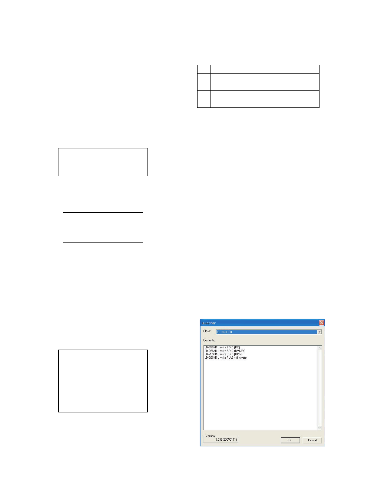
2-6. LD-26SH1U Flash Writing Procedure
[Tool target model]
LD-26SH1U
[Tool operating environment]
• Windows 98/Windows 2000/Windows XP
[Installing procedures]
(1) Make a folder of "c:\fg".
(2) Copy all the files in [launcher3.03e_English_Tool] to c:\fg. (Use the
latest launcher tool.)
(3) Copy all the files in [26SH1U_Flash_Install_Tool(X.XX)] to c:\fg.
(4) Double-click [install.bat] in c:\fg. (If the MS-DOS prompt does not
disappear automatically, manual erase it.)
(5) Copy all the files in [26SH1U_Flash_Install_Data(X.XX)] to c:\fg.
(If the data in the FD are compressed, extract them for use.)
[Operating procedures]
(1) Connect the jig to the PC. (Refer to the separate document.)
(2) Execute c:\fg\launcher.exe.
(3) The following window is displayed. Select the suitable items in
3
[Class] and [Contents] according to the target model.
Select the target model in [Class].
Select LD-26SH1U write FLASH (firmware) in [Contents].
After selection, click [Go].
LD-26SH1U CONNECTION, ADJUSTMENT, OPERATION, AND FUNCTIONS
2 – 12
Page 18
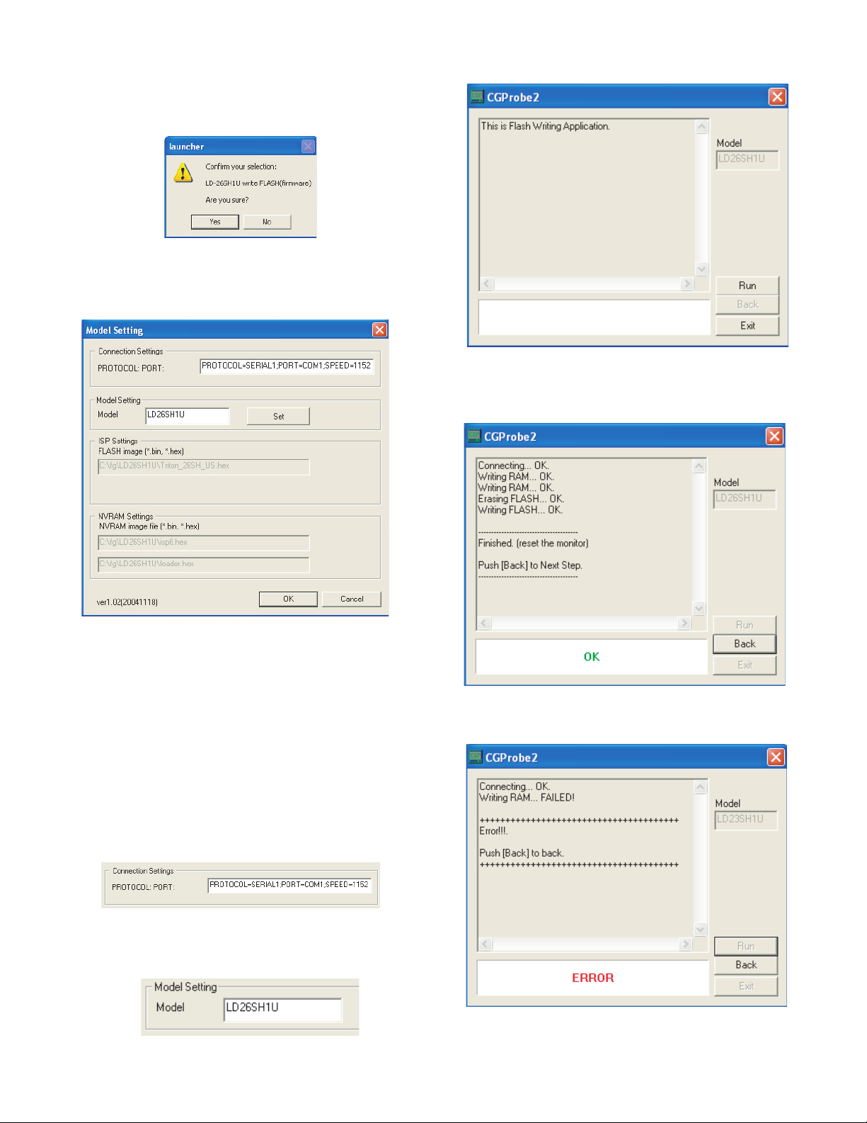
The confirmation window for execution is displayed. If it is OK,
press [Yes]. If not, press [No]. When [No] is pressed, the process
returns to (3). If [Yes] is pressed, the process goes to the next step.
When the button is pressed, the window is changed.
[LD-26SH1U write FLASH (firmware)]]
(4) The following window is displayed. Connect the jig to the monitor.
[Model Name LD26SH1U]
(6) The following window is displayed.
Press [Run] button, and flash writing is started.
(7) After completion of writing, the following window is displayed.
("Finished. (reset the monitor)" is displayed.)
[Setting on the monitor side]
1 : Connect the VGA cable to the jig.
2 : Press and hold [CH
c
] and [VOL/BRIGHT d] and [VOL/BRIGHT e]
keys of the machine, press [POWER] key to turn on the power.
Wait until [ISP MODE] is displayed. When [ISP MODE] is displayed, press [ENTER/BRIGHT MODE] key.
[Setting on the writing tool side]
Execute PORT setting of Connection Settings. (The figure shows the
case where COM1 port is used. When COM4 port is used, write
PORT=COM4.) When setting is made, it is saved.
(5) Check the Model Name.
LD26SH1U
After checking, press [OK] button.
(8) When a writing error occurs, the following window is displayed.
("Error!!!" is displayed.)
LD-26SH1U CONNECTION, ADJUSTMENT, OPERATION, AND FUNCTIONS
2 – 13
Page 19
(9) After normal completion of writing, disconnect the power cable of
the monitor, and connect the cable again. Press [POWER] key of
the monitor to turn OFF.
(10) After normal completion of writing, when [Back] button is pressed,
the window returns to item (6). Then writing to another set can be
made.
Press and hold [CH
c
] and [VOL/BRIGHT d] and [VOL/BRIGHT e]
keys of the monitor, press [POWER] key to turn on the power and
display [ISP MODE]. After pressing [ENTER/BRIGHT MODE] key,
execute procedures from item (6).
(11) To complete FLASH writing, press [Back] button and press [Exit]
button.
(12) Perform [ALL RESET].
Press the [POWER] button to turn off the power. Press and hold
[MENU] button and [ENTER/BRIGHT MODE] button, press
[POWER] button to turn on the power.
[ALL RESET] is displayed.
When [ALL RESET] disappears, press [POWER] button of the
machine to turn off the power.
(13) Firmware version check
After completion of writing, check the firmware version of the set.
Operating procedure :
1
Press and hold [MENU] button and [VOLUME/BRIGHT] button
of the monitor, press [POWER] button of the machine to turn on
the power. Press and hold the three buttons until the following
window is displayed.
2
The firmware version and checksum setting are displayed.
3
Turn off the power of the machine, or press [MENU] button of
the machine to finish the version display.
Version display window :
VERSION & CHECK SUM
VERSION : x.xxx (xxxxxxxx)
CHECK SUM : OK xxxx
END:MENU
<When a writing error occurs>
Check that the PC and the jig are proper connected and that the jig and
the monitor are properly connected. Disconnect the power cable and
connect is again. At that time, the power lamp lights up or does not light
up. Perform the procedures according to the case.
• [When the power lamp lights up]
(1) Press [POWER] key to turn off the power. Press and hold [CH
c
] and [VOL/BRIGHT d] and [VOL/BRIGHT e] keys of the
machine, press [POWER] key to turn on the power. Wait until
[ISP MODE] is displayed. Check to confirm that [ISP MODE] is
displayed, and press [ENTER/BRIGHT MODE] key.
(2) Press [Back] button of the writing tool and perform procedures
of [Operating procedures] (6).
• [When the power lamp does not light]
(1) With the monitor under the same conditions, press Back button
of the writing tool, and perform procedures from [Operating procedures] (6).
*
Check the version, the date, and the checksum (varies
depending on the version).
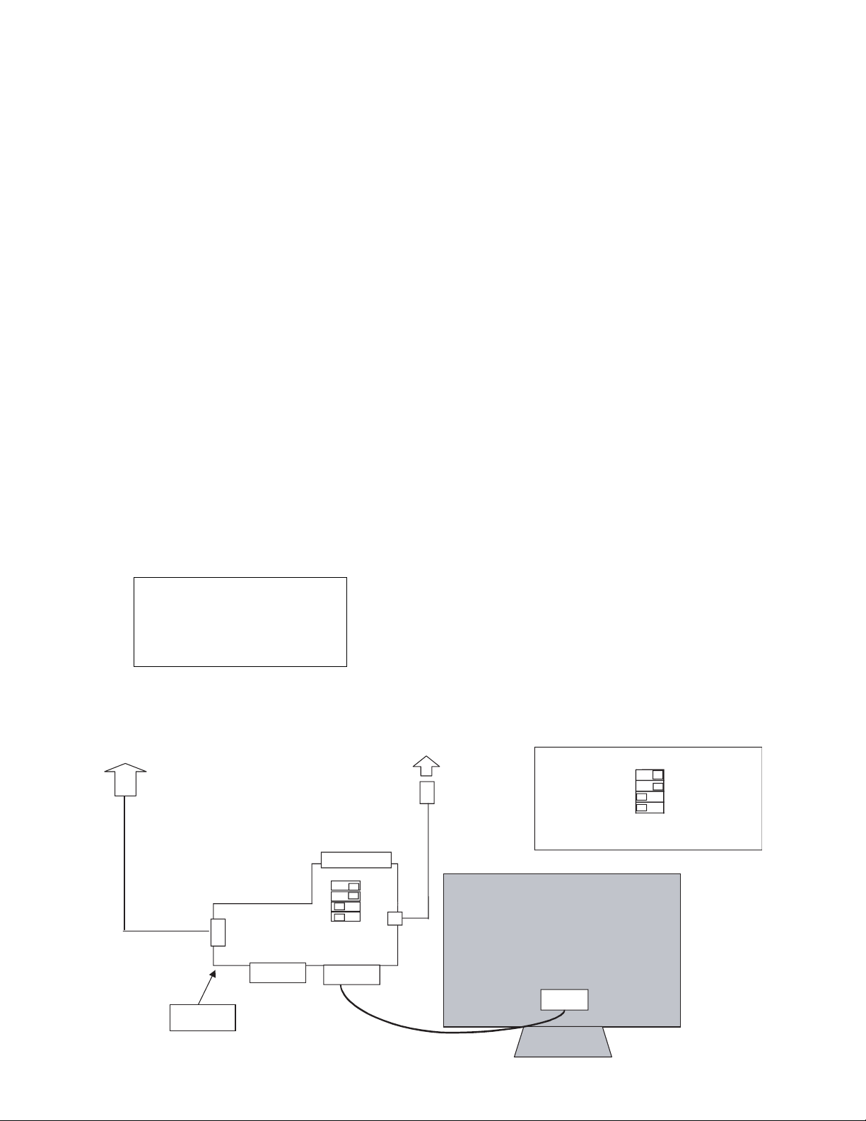
LD-26SH1U FLASH Writing Tool Connection Diagram
Connect to PC series port.
No need to connect the
parallel cable.
Parallel connector
Serial connector
X1
049MP-2
Board
DVI-D
connector
7
LD-26SH1U CONNECTION, ADJUSTMENT, OPERATION, AND FUNCTIONS
VGA
connector
VGA cable
USB
DIP switch direction
Connect to USB
port of PC
USB cable
SW1: Parallel(EDID)
SW
2: AUTO
3: 1502A
SW
SW
4: 1502A T1620
With the parallel connector in the upper side, Right, Right,
Left, and Left from the top.
Serial(PROGRAM)
MANUAL
T
1620
LD-26SH1U
VGA
pin
Back of the machine
2 – 14
Page 20
2-7. LD-26SH1U EDID Writing Procedures
[Tool target model]
LD-26SH1U
[Tool operating environment]
• Windows95/Windows98/Windows 2000/Windows XP
• Set the I/O address of the printer port to 378.
(Refer to the supplementary explanations.)
[Installing procedure]
(1) Make a folder of "c:\fg."
(2) Copy all the files in [launcher3.03e_English_Tool] to c:\fg.
(Use the latest launcher tool.)
(3) Copy all the files in [26SH1U_Flash_Install_Tool(X.XX)] to c:\fg.
1. EDID (PC-DIGITAL/ANALOG) data writing procedures
[Operating procedures]
(1) Connect the jig to the PC. (Refer to the separate document.)
(2) Connect the jig to the monitor. (Refer to the separate document.)
[Setting on the monitor]
Operate with the buttons on the monitor.
1 : Press the [POWER] button of the monitor to turn on the power,
and boost it in the TV mode.
(If the monitor is not in the TV mode, press [INPUT] key to go
to the TV mode.)
2 : Press [MENU] key to display MENU, and press [MENU] key
again to move the cursor to [MODE SELECT] and press
[ENTER/BRIGHT MODE] key.
(5) The confirmation window to check the execution contents is dis-
played. If it is OK, press [Yes]. If not, press [No].
If [No] is pressed, the procedure returns to (4). If [Yes] is pressed,
the procedure goes to the next step.
[LD-26SH1U write EDID (PC)]
(6) When the following window is displayed :
1. The jig may not properly connected to the PC.
Check the connection, and press [OK] button and press [Next]
button.
(7) The following window is displayed. Check the model name.
Enter the serial number the keys and press [Next].
3 : Press [MENU] key in MODE SELECT OSD and move the cur-
d
sor to [DVI SELECT]. Press [
(Factory setting is [AV].)
4 : Connect the DVI-D cable and the VGA cable to the monitor and
the jig.
(3) Execute c:\fg\launcher.exe.
(4) The following window is displayed.
Select the target model in [Class].
Select [LD-26SH1U write EDID (PC)]
After selection, click [Go].
] key to switch to [PC].
in [Contents].
(8) The following window is displayed.
On this window, EDID writing and verifying are performed. If the
operation is terminated halfway, check the connection.
When writing is completed, the window of item (7) is displayed.
LD-26SH1U CONNECTION, ADJUSTMENT, OPERATION, AND FUNCTIONS
2 – 15
Page 21
(9) Set the [DVI SELECT] item switched in procedure (2) ([Setting on
the monitor side]) to [AV].
(10) Press [Power] button to turn off the power.
(11) Connect the jig to the next monitor.
Perform [Setting on the monitor] in procedure (2), and execute from
procedure (7).
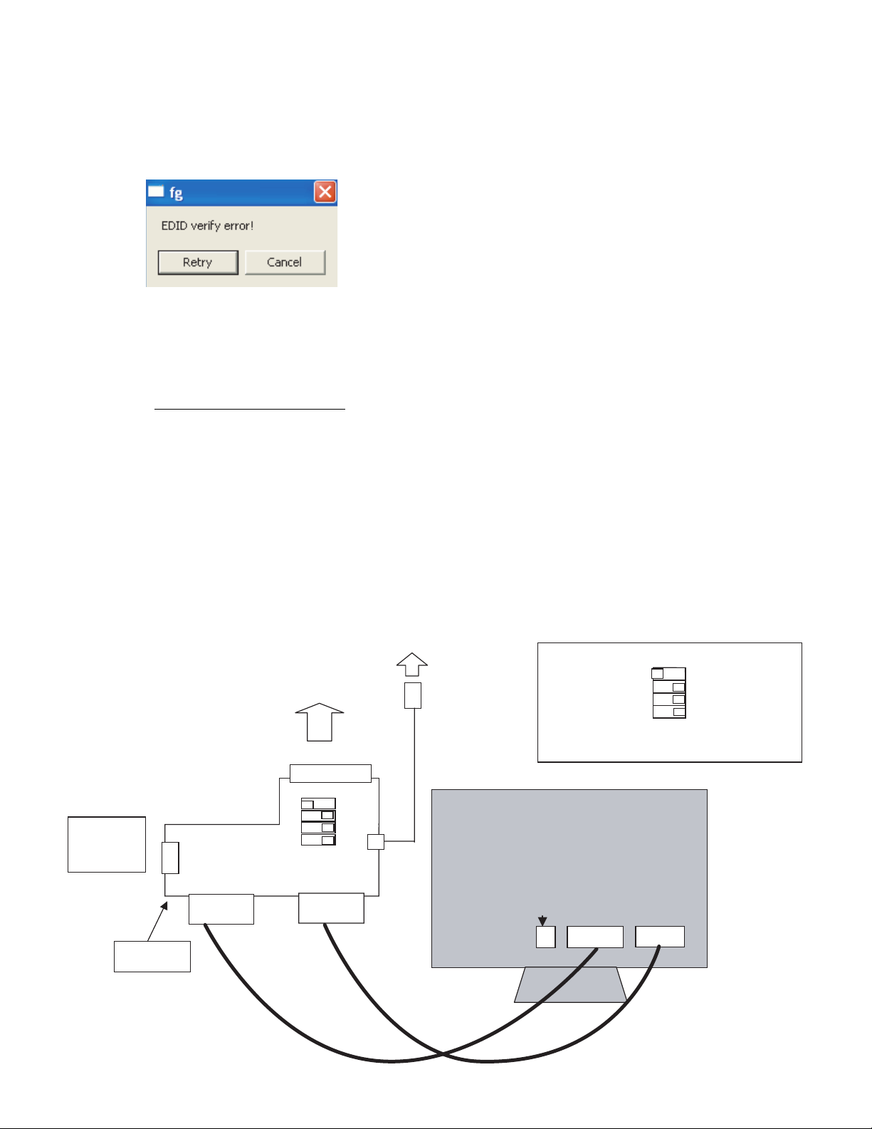
(12) When an error occurs in writing or verifying :
When an error occurs in writing or verifying, the above window is
displayed. When [Retry] button is pressed, EDID writing and verifying are performed again. Normally check the cable connection and
press [Retry] button.
When an error occurs in retry again, press [Cancel] button. When
[Cancel] button is pressed, the window is forcibly changed to the
next window, however EDID is not properly written.
(13) When writing is normally completed or when [Cancel] button is
pressed in EDID error window, the procedure returns to (8).
LD-26SH1U EDID(PC-DIGITAL/ANALOG) date writing tool connection diagram
Connect to
the printer port of PC
Connect to USB
port of PC.
USB cable
Parallel connector
No need to
connect a
serial cable.
X1049MP-27
Serial connector
DVI-D
connector
Board
connector
DVI-D cable
VGA
USB
VGA cable
Back of the machine
HDMI pin
DIP switch setting
SW1 : Parallel (EDID) Serial (PROGRAM)
SW2 :
SW3 : 1502A T1620
SW4 :
1502A T1620
AUTO
MANUAL
With the parallel connector in the upper side, Right,
Right, Left, and Left from the top.
LD-26SH1U
VGA pin
DVI pin
LD-26SH1U CONNECTION, ADJUSTMENT, OPERATION, AND FUNCTIONS
2 – 16
Page 22
2. EDID (HDMI) data writing procedures
[Operating procedures]
(1) Connect the jig to the PC. (Refer to the separate document.)
(2) Connect the jig to the monitor. (Refer to the separate document.)
[Setting on the monitor side]
1 : Press [POWER] key of the monitor to turn on the power.
2 :
Connect the DVI-HDMI conversion cable to the monitor and the jig.
(3) Execute c:\fg\launcher.exe.
(4) The following window is displayed.
Select the target model in [Class].
Select "LD-26SH1U write EDID (HDMI)"
After selection, click [Go].
.
in [Contents].
(7) The following window is displayed.
On this window, EDID writing and verifying are performed. If the operation is terminated halfway, connection may be improper. Check it.
(8) When writing is completed, the following window is displayed.
(5) The confirmation window is displayed. If it is OK, click [Yes]. If not,
click [No]. When [No] is clicked, the procedure goes to (4). If [Yes] is
clicked, EDID writing is started.
[LD-26SH1U write EDID (HDMI)]
(6) When the following window is displayed.
1. The jig may not be connected to the PC properly.
(9) Press [Power] button to turn off the power.
(10) Connect the jig to the next monitor.
Press [Next] button and repeat EDID writing to the next monitor.
(11) When an error occurs in writing or verifying:
When an error occurs in writing or verifying, the above window is
displayed. When [Retry] button is pressed, EDID writing and verifying are performed again. Normally check the cable connection and
press [Retry] button.
When an error occurs in retry again, press [Cancel] button. When
[Cancel] button is pressed, the window is forcibly changed to the
next window, however EDID is not properly written.
(12) When writing is normally completed or when [Cancel] button is
pressed in EDID error window, the procedure returns to (8).
Check the connection, and press [OK] button, and press [Next]
button.
LD-26SH1U CONNECTION, ADJUSTMENT, OPERATION, AND FUNCTIONS
2 – 17
Page 23
LD-26SH1U EDID (HDMI) date writing tool connection diagram
Connect to
the printer port of PC
Parallel connector
Connect to USB
port of PC.
USB cable
DIP switch setting
SW1: Parallel(EDID) Serial (PROGRAM)
SW2:
SW3: 1502A T1620
SW4: 1502A T1620
AUTO
MANUAL
With the parallel connector in the upper side, Right,
Right, Left, and Left from the top.
No need to
connect a
serial cable.
X1049MP-27
Serial connector
DVI-D
connector
Board
VGA
connector
USB
DVI-HDMI transfer cable
3. EDID (DVI-AV) data writing procedures
[Operating procedures]
(1) Connect the jig to the PC. (Refer to the separate document.)
(2) Connect the jig to the monitor. (Refer to the separate document.)
[Setting on the monitor]Operate with the buttons on the monitor.
1 : Press [POWER] button of the monitor to turn on the power,
and boost it in the TV mode.
(If the monitor is not in the TV mode, press [INPUT] key to go
to the TV mode.)
2 : Press [MENU] key to display MENU, and press [MENU] key
again to move the cursor to [MODE SELECT] and press
[ENTER/BRIGHT MODE] key.
3 : Press [MENU] key in MODE SELECT OSD and move the cur-
sor to [DVI SELECT]. Press [
setting is [AV].)
4 :
Connect the DVI-D cable to the monitor and the jig.
(3) Execute c:\fg\launcher.exe.
(4) The following window is displayed.
Select the target model in [Class].
Select [LD-26SH1U write EDID (DVI-AV)]
After selection, click [Go].
d
] key to switch to [PC]. (Factory
in [Contents].
LD-26SH1U
Back of the machine
HDMI pin
DVI pin
VGA pin
(5) The confirmation window to check the execution contents is dis-
played. If it is OK, press [Yes]. If not, press [No]. If [No] is pressed,
the procedure returns to (4). If [Yes] is pressed, the procedure goes
to the next step.
[LD-26SH1U write EDID (DVI-AV)]
(6) When the following window is displayed :
1. The jig may not be properly connected to the PC.
Check the connection, and press [OK] button and press [Next]
button.
LD-26SH1U CONNECTION, ADJUSTMENT, OPERATION, AND FUNCTIONS
2 – 18
Page 24
(7) The following window is displayed.
On this window, EDID writing and verifying are performed. If the
operation is terminated halfway, check the connection.
(8) When writing is completed, the following window is displayed.
(10) Connect the jig to the next monitor.
Perform [Setting on the monitor] in procedure (2), and execute from
procedure (7).
(11) When an error occurs in writing or verifying :
When an error occurs in writing or verifying, the above window is
displayed. When [Retry] button is pressed, EDID writing and verifying are performed again. Normally check the cable connection and
press [Retry] button.
When an error occurs in retry again, press [Cancel] button. When
[Cancel] button is pressed, the window is forcibly changed to the
next window, however EDID is not properly written.
(12) When writing is normally completed or when [Cancel] button is
pressed in EDID error window, the procedure returns to (8).
(9) Press [Power] button to turn off the power.
LD-26SH1U EDID (DVI-AV) date writing tool connection diagram
No need to
connect a
serial cable.
Serial connector
DVI-D
connector
Connect to
the printer port of PC
Parallel connector
Board
VGA
connector
USB
X1049MP-27
DVI-D cable
Connect to USB
port of PC.
USB cable
DIP switch setting
SW1: Parallel (EDID) Serial (PROGRAM)
SW2: AUTO MANUAL
SW3: 1502A T1620
SW4: 1502A T1620
With the parallel connector in the upper side, Right,
Right, Left, and Left from the top.
LD-26SH1U
Back of the machine
HDMI pin
DVI pin
VGA pin
LD-26SH1U CONNECTION, ADJUSTMENT, OPERATION, AND FUNCTIONS
2 – 19
Page 25
[Supplementary explanations]
■
Procedures to set the I/O address of the printer port to 378.
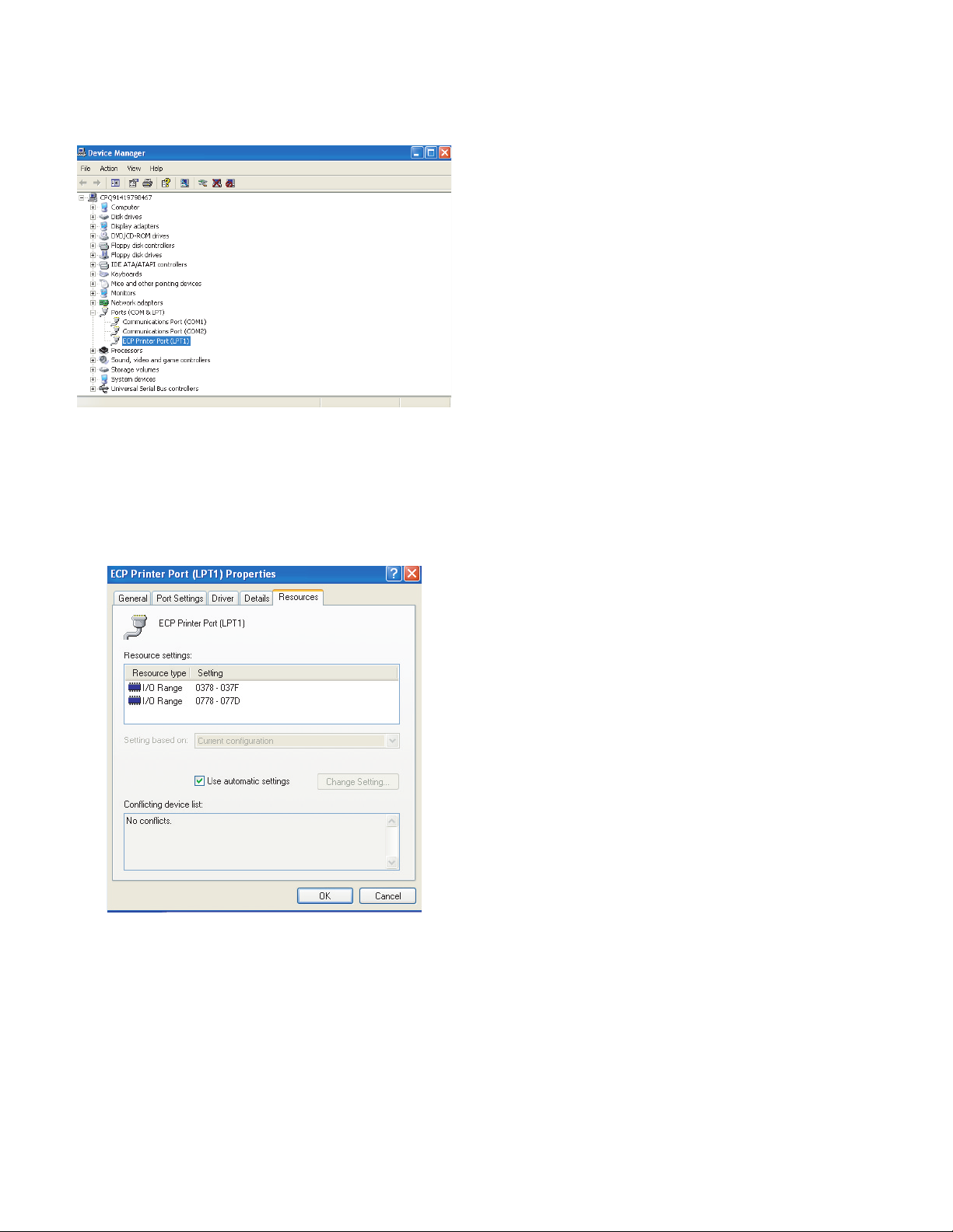
1. Open SYSTEM on the control panel.
2. Open the Device Manager tag, and select the suitable item.
3. Click "+" on the left side of [Ports (COM & LPT) to check to confirm
that there is [Printer Port (LPT1)]. ([ECP Printer Port (LPT1)] or
other descriptions are allowed.)
4. Open the property of [Printer Port (LPT1)], and open the resource
tag.
5. Uncheck [Use automatic setting], and select [Basic setting 0000].
(If [I/O range] is set to [0378 - 037F], there is no need to change.)
The destination of file copying is specified as "c:\fg" in the writing
procedures.
However, the destination may be anywhere on the hard disk as
long as all the files are copied to the dame folder.
LD-26SH1U CONNECTION, ADJUSTMENT, OPERATION, AND FUNCTIONS
2 – 20
Page 26

CHAPTER 3. DISASSEMBLY AND ASSEMBLY
1. HINGE UNIT DISASSEMBLY
1. Remove the I/O cover lower 1.
, and remove the hinge cover rear 3.
2. Remove the screw
3. Remove the screw
2
, and remove the hinge unit 5.
4
4
5
4
1
3
2
3. POWER PWB DISASSEMBLY
1. Remove the screw 1, and remove the power source plate 2.
2. Remove the connectors and the screw
PWB
.
4
3
, and remove the power
3
1
3
2
3
4
1
2. HOUSING UNIT DISASSEMBLY
1. Remove the I/O cover 1.
2. Remove the screw
, and remove the housing unit 3.
2
2
2
3
2
2
1
4. LCD UNIT DISASSEMBLY
4-1. I/O INNER COVER AND MB PLATE UNIT DISAS-
SEMBLY
1. Remove the screw 1, and remove the I/O bracket 2 and the I/O inner
cover
.
3
2. Remove the screw
O inner cover lower
3. Remove the screw
, and remove the I/O bracket lower 5 and the I/
4
.
6
, and remove the MB plate unit 8.
7
1
2
7
7
4
7
8
1
1
3
1
4
LD-26SH1U DISASSEMBLY AND ASSEMBLY
3 – 1
5
4
4
6
Page 27

4-2. HINGE SUPPORT DISASSEMBLY
1. Remove the screw 1, and remove the hinge support 2.
4-4. LCD ASSEMBLY DISASSEMBLY
1. Remove the connectors and the screw 1, and remove the LCD
assembly.
1
1
1
2
4-3. SPEAKER UNIT DISASSEMBLY
1. Remove the connector and the screw 1, and remove the speaker unit
L/R
.
2
1
2
1
1
1
1
2
1
4-5. LCD UNIT DISASSEMBLY
1. Remove the screw 1, and pull out the harness from the base plate
, and remove the LCD unit 3.
unit
2
1
2
1
2
1
3
1
LD-26SH1U DISASSEMBLY AND ASSEMBLY
3 – 2
Page 28

CHAPTER 4. TROUBLE SHOOTING
LD-26SH1U TROUBLE SHOOTING
4 – 1
Page 29

LD-26SH1U TROUBLE SHOOTING
4 – 2
Page 30

LD-26SH1U TROUBLE SHOOTING
4 – 3
Page 31

CHAPTER 5. BLOCK DIAGRAM
■
MAIN PWB
J11
J12
J23
J27
1+5V
2+5V
3 3D_DEBUG_SEL
4 DEBUG_SCL_3D
5 DEBUG_SDA_3D
6 MSTR_SDA_5
7 MSTR_SCL_5
8 DEBUG_DETECT
9TXD
10 RXD
11 GND
1 INPUT
2MENU
3OK
4 CHANNEL_UP
5 CHANNEL_DOWN
6 VOLUME_UP
7 VOLUME_DOWN
8GND
1 REDU+
2 GREENU+
3BLUEU+
4NU
5GND
6GND
7GND
8GND
9+5V
10 GND
11 NU
12 A-SDA
13 A-HS
14 A-VS
15 A-SCL
1GND
2 RCA_V1
3GND
4 RCA_L1
5GND
6 RCA_R1
J18
J1
J21
J5
J23
1GND
2R_OUT
3GND
4L_OUT
5GND
6 CVBS_OUT
1GND
2GND
3 SVIDE01_L_IN
4 SVIDE01_C_IN
1GND
2GND
3Y_OUT
4C_OUT
1 +8V_FAN
2LOCK_FAN1
3GND
1RX2IN-
2RX2IN+
3GND
4NU
5NU
6 DVISCL
7DVISDA
8NU
9RX1IN-
10 RX1IN+
11 GND
12 NU
13 NU
14 DVI_5V
15 GND
16 DVI_CAB
17 RX0IN-
18 RX0IN+
19 GND
20 NU
21 NU
22 GND
23 RXCIN+
24 RXCIN-
J14
1OUT1+
2OUT1-
J20
1OUT2+
2OUT2-
J27
1GND
2 PC_LINE_INL
3GND
4 PC_LINE_INR
5GND
J10
1GND
2RCA_V2
3GND
4 RCA_L2
5GND
6 RCA_R2
J7
1+12V_P
2+12V_P
3GND
4GND
5 +5V_P
6 +5V_P
7GND
8GND
9 +3.3V_P
10 +3.3V_P
11 GND
12 GND
13 +5V_SB_P
14 GND
15 PSON#
16 POWER_OK
J3
1 +8V_FAN
2LOCK_FAN2
3GND
LD-26SH1U BLOCK DIAGRAM
5 – 1
Page 32

J13
J17
1 RESERVED1 LVDS_FRAME 2
3 RESERVED2 LVDS_O_SET 4
5 RESERVED3 LVDS_TEST3 6
7 GND LVDS_TEMP3 8
9 BLADJ LVDS_TEMP2 10
11 GND LVDS_TEMP1 12
13 GND GND 14
15 PBIAS GND 16
39 SELLVDS LVDS_RL 40
37 GND LVDS_UD 38
35 TXA3+ GND 36
33 TXA3- TXB3+ 34
31 GND TXB3- 32
29 TXAC+ GND 30
27 TXAC- TXBC+ 28
25 GND TXBC- 26
23 TXA2+ GND 24
21 TXA2- TXB2+ 22
19 GND TXB2- 20
17 TXA1+ GND 18
15 TXA1- TXB1+ 16
13 GND TXB1- 14
11 TXA0+ GND 12
9 TXA0- TXB0+ 10
7 GND TXB0- 8
5NU GND6
3+5V +5V4
1+5V +5V2
J9
1 Y1_IO D1_LINE_1 8
2 GND D1_I/P_D 9
3PB1_IO REV210
4 GND D1_RATIO 11
5 PR1_IO GND 12
6 GND REV3 13
7 REV1 PLUG1_DET 14
J16
1 Y2_IO D2_LINE_1 8
2 GND D2_I/P_D 9
3PB2_IO REV210
4 GND D2_RATIO 11
5 PR2_IO GND 12
6 GND REV3 13
7 REV1 PLUG2_DET 14
J13
J19
1 POWER LED_KEYPAD 2
3 HP_VCC LED2_KEYPAD 4
5 HEAD_PHONE_R GND 6
7 HEAD_DETECT IR_DATA_IN 8
9 HEAD_PHONE_L +5V 10
11 VD_GND BTN_DETECT 12
1GND GND2
3 RCA_IN_R3 SVIDEO0_L_IN 4
5GND GND6
7 RCA_IN_L3 SVIDEO0_C_IN 8
9GND GND10
11 RCA_V3 S2_DETECT_2 12
13 GND GND 14
15 +5V_VD MSTR_SDA_5 16
17 NU GND 18
19 NU MSTR_SCL_5 20
LD-26SH1U BLOCK DIAGRAM
5 – 2
Page 33

■ SUB PWB
J2
J6
1 HEADPHONE_VOC
2 HEAD_PHONE_L_SW
3 HEAD_PHONE_R_SW
4 HP_DECT
5GND
6NU
7GND
8GND
1AV3_C
2GND
3 AV3_Y
4GND
5GND
6NU
7GND
8 RCAV3
9GND
10 RCA_L3
11 GND
12 RCA_R3
J703
1GND GND2
3 RCA_IN_R3 SVIDEO0_L_IN 4
5GND GND6
7 RCA_IN_L3 SVIDEO0_C_IN 8
9GND GND10
11 RCA_V3 S2_DETECT_2 12
13 GND GND 14
15 +5V_VD MSTR_SDA_5 16
17 NU GND 18
19 NU MSTR_SCL_5 20
J701
J702
1 INPUT
2MENU
3OK
4 CHANNEL_UP
5 CHANNEL_DOWN
6 VOLUME_UP
7 VOLUME_DOWN
8GND
1 POWER LED_KEYPAD 2
3 HP_VCC LED2_KEYPAD 4
5 HEAD_PHONE_R GND 6
7 HEAD_DETECT IR_DATA_IN 8
9 HEAD_PHONE_L +5V 10
11 VD_GND BTN_DETECT 12
LD-26SH1U BLOCK DIAGRAM
5 – 3
Page 34

CHAPTER 6. HARDWARE DESCRIPTION
1. CIRCUIT DESCRIPTIONS
1-1. TV TUNER UT13 (VT2U5JF559)
The VT2U5JF559 is a TV tuner of the NTSC system which is popularly
used in the U.S.A. (PIF45.75MHz)
It operates on the power voltage of 5V (6, 7 pins) and the tuning voltage
of 30V (9 pin). The voltage of 30V is boosted and generated by the PU1
peripheral circuit.
Tuning is controlled by the I2C bus (4, 5 pins), and the video signal
(1Vp-p) is outputted to 19 pin and supplied to the video decoder U19.
Also, the FM signal (about 50mVp-p) of sound SIF is outputted to 15
pin, and supplied through SIF_AMP (Q11) to the audio processor U9.
The audio monaural output (16 pin) is not used in this model.
The AGC voltage output (7pin) falls below 4.5V when the electric field
becomes 60dB or more. This voltage is used in automatic tuning. The
twelve channels of stronger wave have priorities to be selected and
saved in the memory.
When tuning is performed correctly, the AFT voltage (12 pin) becomes
about 2.4V. (100KHz/1V)
This voltage is controlled by the microprocessor to be 2.4V, performing
correct tuning.
1-2. VIDEO SIGNAL PROCESS
1-2-1. AV input selector U35 (CXA2069Q)
This AV selector IC selects the external composite video signal input
pin, the S pin input, the video, and the sound signal from the TV tuner.
Selection is made with the I2C of 33, 34pin.
The output composite signal is supplied to the video coder U19
(VPC3230D) through the 3-dimentional Y/C separations IC (U17) .
The input from the S pin is supplied directly to U19.
1-2-2. 3-dimentional Y/C separation U23 (UPD64084)
The UPD64084 is an adaptive Y/C separation IC used for the purpose
of separation of the composite signal of the brightness signal of tuner
images and the color signal into the bright signal and the color signal.
The composite video signal outputted from the AV input selector U35
(53 pin) is inputted to 93pin through the low pass filter (U29) circuit.
The brightness signal separated in Y/C is outputted from 89pin ( (AYO),
and the color signal is outputted from 88pin (AC0). They are supplied to
the video decoder (U19) through the low pass filter (U24) and the band
pass filter (U22).
1-2-3. Video decoder U19 (VPC3230D)
The VPC3230D is a video decoder IC which converts Y/C separation
signals into digital Y/Pb/Pr signals.
The composite video signal is inputted from the tuner and the external
input pin, and Y/C separated, and inputted from 75pin and 72pin. The
Y/C signal from the S pin is directly inputted to 74pin and 71pin, and
processed as the S signal, and converted into the digital Y/Pb/Pr signals and outputted.
The output is inputted to the IP conversion U33.
1-2-4. Video A/D Converter U37 (MST9883C)
This is an A/D converter which converts analog Y/Pb/Pr signals into digital RGB signals. The Y/Pb/Pr signals inputted from the component
input pin are passed through the low pass filter (U46) to 48 pin, 43 pin,
and 54 pin, and converted into digital RGB signals and inputted to the
IP conversion U33.
1-2-5. IP conversion U33 (FLI2310)
The FLI2310 performs IP conversion of the interlace digital Y/Pb/Pr signal from the video decoder (U19) into the progressive digital RGB signal, and performs IP conversion of the digital RGB signal from U37, and
outputs it to the scaler U34.
1-2-6. Scaler & CPU U34 (gm1501)
The gm1501 allows direct input of the analog RGB signal/digital DVI
signal for PC, and converts the digital RGB input into the specified
screen size, and outputs the LVDS signal to the LCD module.
It is also provided with microprocessor functions, and controls many
IC's according to Flash memory (U42) information.
As additional functions, it is provided with PC input, PinP (Picture in Picture) of tuner and external video input, frame rate change, and OSD
(On-Screen Display).
1-3. AUDIO SIGNAL PROCESS
1-3-1. Audio processor U9(MSP3440G)
The MSP3440G is an audio processor which processes audio signals.
The MSP3440G decodes the SIF signal input (67pin) of the tuner output
into a proper format such as stereo or monaural, sets the sound quality
by Bass and Treble, sets the sound volume (fixed) according to each
input source, and performs other audio signal processes.
The external input signal (56, 57pin) selected by the input selector U35
(CXA2069Q) and the PC AUDIO input (47, 48pin) are selected, and
delay and Dolby signal process are performed, and they are outputted
from 27 and 28pins to the speaker amplifier and from 24 and 25 pins to
the headphone amplifier.
They are also outputted from 36 and 37pins through the input selector
U35 (CXA2069Q) to the external output pin.
1-3-2. Digital audio delay U6 (NJU26901)
The NJU26901 is a delay IC which delays the output time of audio signals.
When an audio signal is inputted to 1pin, it performs delay process of
the specified time and outputs the signal to 7pin.
1-3-3. Digital audio processor U13 (NJU26106)
The NJU26106 is a digital audio processor which decodes stereo audio
signals.
Stereo signals inputted to 25pin are decoded to virtual Dolby surround and
outputted from 3pin.
1-3-4. Speaker driver U1 (LA4636)
The LA4636 is a power IC of the BTL system, which drives two speakers: L and Rch of 8Ω. Audio signals inputted at 2 and 4 pins are outputted to 8 - 9 pins and 11 ?
12pins in reverse polarity of L and Rch.
The voltage gain is fixed to 35dB. However, mute can be applied by the
control voltage at 6pin.
The voltage at the standby pin (5pin) is controlled by the headphone
detection signal from the headphone pin to shut off the speaker output.
1-3-5. Headphone amplifier U5 (LM4911)
The LM4911 is an audio power amplifier which allows gain adjustment
by an external resistor.
The headphone audio signal inputted at 1, 5pin is outputted to 7, 9pin (L
& Rch).
LD-26SH1U HARDWARE DESCRI PTION
6 – 1
Page 35

1-4. INVERTER UNIT
(HIGH VOLTAGE SIDE: RDENC2159TPZZ,
LOW VOLTAGE SIDE: RDENC2161TPZZ)
For lighting the 14-lamp backlight (striplight) of the LCD panel.
It allows ON-OFF control and brightness (Duty light control system)
control.
The operating power source is supplied from the 12V output connector
CN201 for the power unit inverter directly with the cable.
The inverter PWB is composed of two PWB's: one on the high voltage
side with the control and the output circuits and the other on the low
voltage side for detection of current, and is connected with FFC.
15pin of J13 connector on the main PWB is for ON/OFF control (ON at
5V) of the backlight, and 9pin is for control of the brightness adjustment.
Brightest at 0V. The higher the voltage is, the darker the brightness is.
(Max. 5.0V)
The protection circuit is provided to stop operation when any trouble
occurs in the lamp.
Note: The inverter unit supplies a high voltage of max. 2,000V to the
lamp by the boosting transformer.
Be sure to keep your hand away from the output connector, etc.
when the machine is conducting. It is very dangerous. Use great
care when servicing.
1-5. AC POWER UNIT (DPS190DP)
The PDS190DP is a power unit of multi outputs (12V, 5V, 3.3V, sub 5V)
of general output 190W. The input power specification is AC100 ? 240V
(50/60Hz).
It is provided with the AC input connector CN1, the inverter output connector CN201, and other I/O connector CN202.
The CN201 is used for output of 12V for the inverter. 1- 5 pins and 11 ?
15 pins are GND, 6 ? 10 pins and 16 ? 20 pins are at 12V.
The CN202 has 12V pin (1, 2pin) for the circuits, 5V pin (5, 6pin) for the
circuits, 3.3V pin (9, 10pin) for the circuit, 5V pin (13pin) for the sub
power source, the ON/OFF control input PSON (15pin), the power status output PG (16pin), and the other pins (3, 4, 7, 8, 11, 12, 14 pin) for
GND.
5V and 3.3V are generated from 12V by the DC-DC converter circuit
inside the power source. Protection circuits are provided against an
overvoltage, an overcurrent, and a high temperature. When the power
is shut down, disconnect the AC cord and connect it again to reset.
Note: While AC power is supplied, a voltage is provided to the heat
sink (HS1, HS2, HS3) on the primary side. Use great care to
avoid an electrical shock when servicing. (The heat sink HS4
near the output connector is at GND level, and safe when
touched.)
1-6. REMOTE CONTROL
This is a remote control of infrared system.
When the remote control key is pressed, infrared rays are radiated in
pulses. (Remote control code)
The remote control light receiving section U7 is provided in the front
side of the unit.
When it receives infrared pulses, it converts infrared rays into a voltage.
The information is transmitted to the microprocessor to perform proper
processes.
LD-26SH1U HARDWARE DESCRI PTION
6 – 2
Page 36

B
B
B
834
VCC
A0A1A2
U40
76512
0.1U
C300
12
TP30
1
B
0.1U
+5V_VD
12
834
VCC
A0A1A2
U24
76512
C366
50V
0603
TP13
1
OS
GND
SDA
SCL
50V
0603
OS
GND
SDA
SCL
LM75_SO
284500075007
SO8
D
D
D
D
1/26
12345678
12345678
12345678
12345678
FD2
FD_DOT040
FD4
FD_DOT040
FD3
FD_DOT040
FD1
FD_DOT040
1
1
1
1
FD701
FD_DOT040
FD704
FD_DOT040
FD703
FD_DOT040
FD702
FD_DOT040
1
1
1
1
C
C
C
C
+5V_VD
A
21
21
21
21
VD_GNDVD_GND
3
3
3
3
LM75_SO
284500075007
SO8
MTG14
ID3.5/OD8
MTG12
ID3.5/OD8
MTG9
ID3.5/OD8
MTG8
ID3.5/OD8
MTG3
ID3.5/OD8
VD_GND VD_GND
I2C address : 90
SHORT-SMT4
JO15
1 2
7
6
1
5
2
4
3 8
7
6
1
5
2
4
3 8
7
6
1
5
2
4
3 8
7
6
1
5
2
4
3 8
7
6
1
5
2
4
3 8
GNDGND
GND
IO_GND
SHORT-SMT4
JO702
SHORT-SMT4
JO701
SHORT-SMT4
JO14
1 2
1 2
1 2
TVTUNER_GND
TUNER_MTG_GND
1
VD_GND
MTG31
ID1.2/OD1.78/SLD5
1
VD_GND
MTG30
ID1.2/OD1.78/SLD5
For AMP HEATSINK Only
1 2
1 2
R379 33 0603
R380 33 0603
MSTR_SDA_5(3,14,17,18)
For ESD
1
TP37
TOUCHPAD_METAL16
1
TP36
TOUCHPAD_METAL16
1
TP742
TOUCHPAD_METAL16
MSTR_SCL_5(3,14,17,18)
VD_GND
GND GND
Close to PC audio in
Close to DVI
Close to D-SUB
+5V_VD
1 2
1 2
R338 33 0603
R337 33 0603
MSTR_SCL_5(3,14,17,18)
MSTR_SDA_5(3,14,17,18)
MTG23
ID3.8/OD8.0
MTG32
ID3.8/OD8.0
FOR ESD
MTG4
ID3.5/OD8.0
I2C address : 96
1
GND
1
IO1_GND
IO_GNDVD_GND
SHORT-SMT4
JO4
1 2
1
History
CHAPTER 7. CIRCUIT DIAGRAM & PWB LAYOUT
1. CIRCUIT DIAGRAM
87654
87654
87654
87654
B
B
B
D
D
D
D
C
C
C
C
B
A A
A A
A A
A
LD-26SH1U CIRCUIT DIAGRAM & PWB LAYOUT
7 – 1
Page 37

B
B
B
SYNCDET (17)
10K
0603
D_CONNECT_SEL (19)
AMP_STBY (16)
LVDS_UD (8)
LVDS_RL (8)
D_CONNECT_SEL
AMP_STBY
SYNCDET
1 2
1 2
1 2
1 2
1 2
1 2
R401 100 0603
R426 100 0603
R428 100 0603
R836 100 0603
R403 100 0603
R402 100 0603
AB2
AB1
AC3
AC2
AC1
AD1
OCMDATA14
OCMDATA13
OCMDATA12
OCMDATA11
OCMDATA10
D1_I/P (19)
HP_MUTE (16)
HP_MUTE
1 2
R404 100 0603
OCMDATA6
OCMDATA7
AE1
AF1
OCMDATA9
OCMDATA8
OCMDATA7
B
C343
12
OCMDATA4
OCMDATA5
AD2
AE2
AF2
OCMDATA6
OCMDATA5
0.1U
16V
0603D_1
OCMDATA2
OCMDATA1
OCMDATA3
AD3
AE3
AF3
OCMDATA4
OCMDATA3
OCMDATA2
GND
OCMDATA[0..7]
OCMDATA0
AD4
OCMDATA1
OCMDATA0
+5V_VD
MSTR_SCL (9,11,14,15,23)
MSTR_SCL_5 (1,14,17,18)
1 2
R41 10K 0603
+5V_VD
+3.3VS_DIG
OCMDATA[0..7] (6)
+3.3V
D
S
R195
12
R194
12
R237
12
R235
12
R236
5.6K
12
R234
5.6K
12
DS
10K/NA
10K/NA
5.6K
5.6K
0603
0603
+3.3VS_DIG
Q707
2N7002
G
0603
0603
0603
0603
MSTR_SCLU
3
4
1A1
1A2
1B1
1B2
U21
256
MSTR_SCL MSTR_SCL_5U
MSTR_SCL_1601
TXD (7 )
TXD
M2
OCM_UDI
IR_DATA0 (12)
IR_DATA (12)
IR0
RESET#
IR_DATA
K1M4M3P4P3
IR1
RESETn
C
C
C
C
+5V
C187
12
+3.3V
OCM_WE# (6)
MSTR_SDA_1601
MSTR_SCL_1601
1 2
1 2
OCM_RE#
OCM_WE#
R459 33 0603
R460 33 0603
R3R2R1L1L2P2P1
IR0
OCM_WEn
MSTR_SCL
MSTR_SDA
FOR I2C PORT
1U
0603
VD_GND
R193
12
12
R845
TP738
1
12
OCM_RE# (6)
D_MODE_SEL2 (19)
HEADPHONE_DETECT (12,16)
OCM_CS# (6)
D_MODE_SEL1 (19)
I2C_CTL
HEADPHONE_DETECT
OCM_CS#
T4
OCM_REn
ROM_CSn
OCM_INT2
OCM_INT1
OCM_CS2n
OCM_CS1n
10K
10K
R830
OCMADDR19 (6)
OCM_CS0n
J11
123456789
10
11
GND1
MSTR_SCL_5
3D_DEBUG_SEL
MSTR_SDA_5
1 2
1 2
R191 33 0603
R192 33 0603
DEBUG_SCL_3D(20)
DEBUG_SDA_3D(20)
0603
0603
RXD
TXD
DEBUG_DETECT
10K/NA
0603
GND
DEBUG_DETECT(4)
OCMADDR[0..18] (6)
OCMADDR[0..18]
OCMADDR11
OCMADDR13
OCMADDR17
OCMADDR12
OCMADDR16
OCMADDR14
OCMADDR15
OCMADDR16
OCMADDR15
OCMADDR14
OCMADDR10
OCMADDR13
OCMADDR12
OCMADDR11
OCMADDR10
OCMADDR7
OCMADDR9
OCMADDR8
OCMADDR9
OCMADDR8
OCMADDR5
OCMADDR6
OCMADDR7
OCMADDR6
OCMADDR18
OCMADDR19
T3T2T1U4U3U2U1V4V3V2V1W3W2W1Y3Y2Y1
OCMADDR19
OCMADDR18
OCMADDR17
GND2
MA/11PX1/RA
OCMADDR3
OCMADDR4
OCMADDR5
OCMADDR4
ACES
87213-1100
P/N = 291000021105
12
+3.3VS_DIG
OCMADDR0
OCMADDR1
OCMADDR2
AA3
AA2
AA1
OCMADDR3
OCMADDR2
OCMADDR1
OCMADDR0
VD_GND
R427
PSON (21)
POWER_OFF
1 2
R835 100 0603
AB3
OCMDATA15
D
D
D
D
2/26
12345678
12345678
12345678
12345678
GND
123
4
A0A1A2
GND
VCCWPSCL
SDA
U705
M24C32
SO8
P/N = 283467930005
876
5
GND
0.1U
50V
C864
0603
C341
12
R399
SOT143
12
0.01U
0.1U
0603
100K
0603
0.1U
C314
0603
MSTR_SCL_1601
MSTR_SDA_1601
50V
GND
50V
0603
12
GND GND
RP27
10K*4
876
123
G_SVDATA2
G_SVDATA0
G_SVDATA1
G_SVDATA0
G_SVDATA1
G_SVDATA2
C16
B16
A16
SVDATA0
SVDATA1
1206
RP701
5
876
4
123
G_SVDATA4
G_SVDATA5
G_SVDATA3
G_SVDATA5
G_SVDATA3
G_SVDATA4
D15
C15
B15
SVDATA2
SVDATA3
SVDATA4
10K*4
1206
5
4
G_SVDATA6
G_SVDATA7
G_SVDATA7
G_SVDATA6
A15
D14
SVDATA5
SVDATA7
SVDATA6
TP725
1
G_SVDV
A17
SVDV
GND
TP26
TP25
1
1
G_SVODD
G_SVS
A14
B14
SVODD
SVVSYNC
R890 10K 0603
TP731
TP727
1
1
G_SHS
G_SVCLK
C14
D16
SVHSYNC
1 2
SVCLK
GND
RXD (7)
RXD
M1
OCM_UDO
+3.3V
RESET#
R40000603
1 2
12
1
2
GND
RESET
VCC
MN
U39
IMP811
4
3
10K
0603
R425
C342
12
12
+3.3V
A
+5V_VD
MSTR_SDA_5 (1,14,17,18)
MSTR_SDA (9,11,14,15,23)
1 2
R40 10K 0603
DS
D
Q708
2N7002
S
G
MSTR_SCL_3D (20)
MSTR_SDA_3D (20)
MSTR_SDA_5U
MSTR_SDAU
MSTR_SDA_3D
MSTR_SCL_3D
781114171821221
1A3
1A4
1A5
2A1
2A2
2A3
2A4
1B3
1B4
1B5
2B1
2B2
2B3
2B4
9
10151619202324
MSTR_SDA
MSTR_SDA_1601
1 2
R375 0 0603
+3.3VS_DIG
3D_DEBUG_SEL
I2C_CTL
2A5
1OE#
2B5
VCC
1 2
R384 0/NA 0603
+5V
+5V_VD
12
13
2OE#
GND
12
C381
12
R250
10K
0603
SN74CBTD3384
TSSOP24
P/N = 282074338403
1U
0603
21
21
21
21
3
3
3
3
VD_GND
VD_GND
D_DETECT (19)
R857
100K
0603
12
D_RESOLUTION
C863
CAP;33P ,50V,5% ,0603,NPO,SMT
272075330302
12
X7
C862
CAP;33P ,50V,5% ,0603,NPO,SMT
272075330302
12
+3.3V_PLL +3.3V_PLL
GM1501_ 1
R249
150K
12
C262
12
XTAL
1 2
14.31818MHZ
D
D
D
D
0603
0.1U
16V
0603D_1
TCLK
Crystal C-load=16 pF
U34A
DVI_SCL
DVI_SDA
RX0+
RX0-
RX1+
RX1-
RX2+
RX2-
RXC+
RXC-
NC_1
NC_0
REXT
BLUE-
BLUE+
GREEN-
GREEN+
RED-
RED+
SOG
NC_2
VGA_SCL
VGA_SDA
AHSYNC
AVSYNC
EXTCLK
XTAL
TCLK
NC_3
NC_4
ACS_RSET_HD
VRED0
VRED1
VRED2
VRED3
VRED4
VRED5
VRED6
VRED7
VGRN1
VGRN2
VGRN3
VGRN4
VGRN5
VGRN6
VGRN7
VGRN0
VBLU0
VBLU1
VBLU2
VBLU3
VBLU4
VBLU5
VBLU6
VBLU7
VCLK
VODD
VVS
VHS_CSYNC
VDV
VCLAMP
LBADC_IN3
LBADC_IN2
LBADC_IN1
LBADC_RETURN
PWM0
PWM1
PWM2
OCM_TIMER1
GM1501-CF
L4
L3
A8B8A9
B9
A6
B6
B1
N4
N3
GND
RX1-(7)
RX0-(7)
RX0+(7)
RX1+(7)
DVI_SDA(7)
DVI_SCL(7)
B2
C5
D5
A10
RX2+(7)
C1C2D1D2C3A1N2
B10
B11
SOG(7)
RED-(7)
RED+(7)
BLUE-(7)
BLUE+(7)
GREEN-(7)
RX2-(7)
GREEN+(7)
RXC-(7)
RXC+(7)
1 2
R825 249 0603 1%
+3.3V_DVI
F1
K3
K2
N1
R4
G4
G3
B19
A19
B18
A18
B22
A22
B21
A21
A23
B25
A25
B24
A24
B23
A20
B20
C19
D18
C18
C17
C22
D21
C21
D24
C24
TCLK
XTAL
RED_HD3
RED_HD2
RED_HD4
RED_HD5
ACS_RESET_HD
RED_HD6
RED_HD0
RED_HD7
R834
12
GND
10K 0603D_1
RED_HD1
1%
1 2
R832 3.3K 0603
GND
RED_HD[0..7]
RED_HD[0..7](9)
AVS(7)
AHS(7)
VGA_SCL(7)
VGA_SDA(7)
C
C
C
C
GREEN_HD2
GREEN_HD0
GREEN_HD1
GREEN_HD4
GREEN_HD5
GREEN_HD6
GREEN_HD3
BLUE_HD0
BLUE_HD1
GREEN_HD7
GREEN_HD[0..7]
GREEN_HD[0..7](9)
BLUE_HD2
BLUE_HD3
BLUE_HD4
BLUE_HD5
C23
BLUE_HD6
BLUE_HD7
BLUE_HD[0..7]
B17
C20
D19
D20
C26
C25
1 2
1 2
LED_KEYPAD
R344 10K 0603
R330 10K 0603
GND
GND
BLADJ(8)
LED_KEYPAD(12)
HD_VVS(9)
HD_VHS(9)
HD_SOG(9)
HD_VCLK(9)
BLUE_HD[0..7](9)
B
B
B
B
A12
D26
D25
VFC_PWM
LED2_KEYPAD
VFC_PWM(19)
LED2_KEYPAD(12)
TUNER_AGC(17)
B12
C12
D12
D_RESOLUTION
TUNER_AFT(17)
BGA352_64
0.01U
C265
12
0.01U
C425
12
0.01U
C263
12
GND
0603
GND
0603
GND
0603
GND
87654
87654
87654
87654
A A
A A
A A
A
LD-26SH1U CIRCUIT DIAGRAM & PWB LAYOUT
7 – 2
Page 38

B
B
B
D
D
D
D
C
C
C
C
3/26
HDR/MA-8
ACES
88260-0800
12345678
12345678
12345678
12345678
TXA3+ (8)
TXA3- (8)
TXAC- (8)
TXAC+ (8)
TXA1- (8)
TXA2- (8)
TXA1+ (8)
TXA2+ (8)
TXA0- (8)
TXA0+ (8)
TXA2-
TXA3-
TXA1+
TXAC+
TXA1-
TXAC-
TXA0+
TXA0-
TXA2+
TXA3+
TXB0- (8)
TXBC- (8)
TXB1- (8)
TXB3- (8)
TXB0+ (8)
TXB2+ (8)
TXB1+ (8)
TXBC+ (8)
TXB3+ (8)
TXB2- (8)
TXB1-
TXB0+
TXB0-
TXB2+
TXB2-
TXB1+
TXBC+
TXBC-
TXB3-
TXB3+
PLUG1_DET (19)
LVDS_Temp3 (8)
LVDS_Temp2 (8)
1 2
1 2
R817 100 0603
R818 100 0603
PLUG1_DET
+3.3V
DEBUG_DETECT (3)
R367
10K
0603
12
R305
10K
0603
12
R307
10K
0603
12
10K*4
1206
RP13
1
8
2
7
3
6
4
5
LOCK_FAN2 (21)
R815
100
0603
1 2
TP721
1
TXAC-
TXA0+
TXA1+
TXA3-
TXAC+
TXA3+
MB_ID
TXA0-
TXA2+
TXA2-
TXA1-
J12
1234567
INPUT
MENU
LVDS_Temp1 (8)
123
1 2
876
R814 100 0603
RP14
OK
VOLUME_UP
CHANNEL_DOWN
CHANNEL_UP
4
1 2
5
R308 4.7K 0603
R306 4.7K 0603
4.7K*4
1206
P/N = 291000000027
8
GND1
VOLUME_DOWN
TP737
1
1 2
1 2
R364 4.7K 0603
GND2
GND
POWER (12,16,21)
BTN_DETECT (12,14,18)
R370
0/NA
0603
1 2
G
Q51
2N7002
R374
10K
0603
DS
1 2
+3.3V
SHP_DEBUG (7)
D2_I/P (19)
PLUG2_DET (19)
COUNT1 (14)
COUNT0 (14)
TP736
TP733
1
1
1 2
1 2
R345 0 0603
R346 0 0603
D
S
0.1U
50V
C294
0603
12
GND
TP734
TP735
TP732
TP729
1
1
1
1
TXB1+
TXBC-
TXB2-
TXB0+
TXB1-
TXB2+
TXB3-
TXB3+
TXBC+
B
R833
10K
0603
12
R366
10K
0603
12
R365
10K
0603
12
R371
10K
0603
12
+3.3V
GND
R369
5.6K
0603
12
+3.3V+3.3V
R368
5.6K/NA
0603
12
LA4635_MUTE (16,18)
TP740
TP730
TP741
TP739
1
1
1
1
JTAG_TDI/SDA
JTAG_TDO
JTAG_TRST
TXB0-
SEC_SCL
SEC_SDA
JTAG_TMS
JTAG_TCK/SCL
12
LOCK_FAN1 (21)
100
0603
1 2
R762
VGA_CAB (7)
DEV_RESET# (9,14,15,23)
VGA_CAB
DVI_CAB
DEV_RESET#
R828
10K
0603
1K/NA
R393
12
12
R3861K0603
DVI_CAB (7)
12
JTAG_TMS
JTAG_TDI/SDA
JTAG_TRST
JTAG_TDO
JTAG_TCK/SCL
0603
GND GND
1000P
0603
C144
GND
MB ID 1
L: JP( PVT)
R831
10K/NA
0603
H: JP( EVT, DVT)
A
1 2
GND
21
21
21
21
3
3
3
3
FSDQSU0
FSDQSU1
FSDQSU2
FSDQSU3
1 2
1 2
1 2
1 2
R795 33 0603
R789 33 0603
R788 33 0603
R791 33 0603
FSDQS_0
FSDQS_1
FSDQS_2
FSDQS_3
FSDQS_2(6)
FSDQS_3(6)
FSDQS_1(6)
GM1501_2
AD23
AD24
AE24
AF24
AF25
AF26
AE25
AE26
AE8
AF8
AC9
AD9
AE9
AF9
AD10
AE10
AF10
AC11
AD11
AE11
AF11
AF12
AE12
AF13
AE13
AD14
AF14
AE14
AF15
AE15
AF16
AE16
AC7
AF17
AD16
AD7
AD8
AF7
AE7
AF6
AE6
AD6
AF5
AE5
AD5
AC5
AF4
GPIO_G09_B5(DEBLU1)
GPIO_G09_B1(DERED1)
GPIO_G08_B1(DORED1)
GPIO_G08_B0(DORED0)
GPIO_G09_B3(DEGRN1)
GPIO_G09_B2(DEGRN0)
GPIO_G08_B3(DOGRN1)
GPIO_G08_B2(DOGRN0)
GPIO_G09__B4(DEBLU0)
PPWR
PBIAS
NC_5
OEXTR
D_GND_54
A26
B26
AC17
AC16
AD15
OEXTR
PBIAS(8)
ENVGA(8)
LCD POWER ENABLE
BACKLIGHT ENABLE
PPWR---- - -
PBIAS--- -
AE4
GPIO_G09_B0(DERED0)
GM1501-CF
BGA352_64
GND
R823
3.3K
0603
12
GND
10K/NA
10K
0603
R811
+3.3V
0603
R810
MB_ID
MB ID
H: US( DVT), JP( PVT)
1 2
L: US( EVT), JP( EVT,
DVT)
GND
87654
87654
87654
87654
1 2
AD21
AD22
AE21
AF21
AE22
AF22
AE23
A2-(DOGRN4)
AC-(DORED9)
A2+(DOGRN3)
A1+(DOGRN6)
GPIO_G05_B0(DOGRN2)
GPIO_G05_B3(DOGRN5)
FSDATA7/FSDATA28
FSDATA8/FSDQM2
FSDATA9/FSDATA16
FSDATA10/FSDATA11
FSDATA11/FSDATA9
FSDATA12
FSDATA13/FSDQS1
T26
P24
P26
R25
N24
N26
M25
FSDATAU16
FSDATAU9
FSDATAU12
FSDATAU11
FSDQSU1
FSDQMU2
FSDATAU15
FSDATAU17
FSDATAU12
FSDATAU14
FSDATAU13
FSDATAU11
FSDATAU15
FSDATAU16FSDATA16
1234567
10111213141516
8 9
RP9
33*8
FSDATA11
FSDATA12
FSDATA13
FSDATA17
FSDATA15
FSDATA14
AF23
A1-(DOGRN7)
A0-(DOGRN9)
A0+(DOGRN8)
GPIO_G04_B0(DOBLU2)
GPIO_G04_B1(DOBLU3)
GPIO_G04_B2(DOBLU4)
GPIO_G04_B3(DOBLU5)
FSDATA14/FSDATA15
FSDATA15/FSDATA27
FSDATA16/FSDATA26
FSDATA17'FSDATA14
FSDATA18/FSDATA24
FSDATA19/FSDQM1
FSDATA20/FSDATA13
FSDATA21/FSDATA10
L24
L25
P25
N25
N23
M26
M24
FSDATAU27
FSDQMU1
FSDATAU10
FSDATAU26
FSDATAU14
FSDATAU24
FSDATAU13
FSDATAU24
FSDATAU20
FSDATAU19
FSDATAU23
FSDATAU18
FSDATAU22
FSDATAU21
89
10111213141516
1234567
RPX8
RP7
FSDATA20
FSDATA23
FSDATA18
FSDATA21
FSDATA24
FSDATA22
FSDATA19
GPIO_G04_B3(DOBLU6)
GPIO_G04_B4(DOBLU7)
GPIO_G04_B6(DOBLU8)
GPIO_G04_B7(DOBLU9)
GPIO_G07_B0(DERED2)
GPIO_G07_B1(DERED3)
FSDATA22/FSDATA17
FSDATA23/FSDATA8
FSDATA24/FSDQM3
FSDATA25/FSDQS3
FSDATA26/FSDATA30
FSDATA27/FSDATA4
FSDATA28/FSDATA6
J26
K24
R26
R24
H25
G23
G25
FSDATAU3
FSDATAU30
FSDQSU3
FSDQMU3
FSDATAU6
FSDATAU17
FSDATAU4
FSDATAU8
FSDATAU27
FSDATAU31
FSDATAU25
FSDATAU29
FSDATAU26
FSDATAU30FSDATA30
10111213141516
8 9
33*8
RPX8
FSDATA25
FSDATA28 FSDATAU28
FSDATA26
FSDATA31
FSDATA29
FSDATA27
SHIELD[0](DEGRN2)
GPIO_G07_B2(DERED4)
GPIO_G07_B3(DERED5)
GPIO_G07_B4(DERED6)
GPIO_G07_B5(DERED7)
GPIO_G07_B6(DERED8)
GPIO_G07_B7(DERED9)
FSDATA29/FSDATA3
FSDATA30/FSDQS0
FSDATA31/FSDQM0
FSADDR0
FSADDR1
FSADDR2
FSADDR3
F24
F25
F26
AD25
AD26
AC24
AC25
FSDQSU0
FSDQMU0
FSADDRU1
FSADDRU4
FSADDRU0
FSADDRU2
FSADDRU3
FSADDRU1
FSADDRU0
FSADDRU11
FSADDRU10
FSADDRU2
123
4
876
5
RP12
33*4
1206
FSADDR2
FSADDR0
FSADDR1
FSADDR11
FSADDR10
FSADDR[0..11]
FSADDR[0..11](6)
B3-(DEGRN7)
B3+(DEGRN6)
BC+(DEGRN8)
SHIELD[1](DEGRN3)
SHIELD[2](DEGRN4)
SHIELD[3](DEGRN5)
FSADDR4
FSADDR5
FSADDR6
FSADDR7
FSADDR8
FSADDR9
Y24
AB26
AA24
AA25
AA26
AB25
FSADDRU6
FSADDRU5
FSADDRU7
FSADDRU8
FSADDRU9
FSADDRU3
FSADDRU8
FSADDRU4
FSADDRU5
FSADDRU9
123
4
123
876
5
876
RP11
33*4
1206
RP10
33*4
FSADDR5
FSADDR4
FSADDR9
FSADDR8
FSADDR3
BC-(DEGRN9)
SHIELD[4](DEBLU2)
FSADDR10
FSADDR11
U24
AB24
AC26
FSADDRU10
FSADDRU11
1 2
FSADDRU7
FSADDRU6
R797 10 0603
4
5
FSCLK+ FSCLKU+
1206
FSADDR7
FSADDR6
B0+(DEBLU)
B2-(DEBLU4)
B1-(DEBLU7)
B2+(DEBLU3)
B1+(DEBLU6)
SHIELD[5](DEBLU5)
FSCLKp
FSCLKn
FSDQS/FSDATA25
FSDQM0/FSDATA19
L26
T25
U23
U25
FSCLKU-
FSDATAU19
FSDATAU25
FSDQSU2
1 2
R796 10 0603
FSCLK-
FSCLK-(6)
FSCLK+(6)
DVS
DHS
DEN
DCLK
B0-(DEBLU9)
FSDQM1/FSDQM2
FSDQM2/FSDATA20
FSDQM3/FSDATA18
FSWE/FSDATA23
FSCAS/FSDATA22
FSRAS/FSDATA21
T24
V26
V25
V24
U26
FSDATAU23
FSDATAU22
FSDATAU21
FSDATAU20
FSDATAU18
FSCKE FSCKEU
GPIO_G08_B5(DOBLU1)
GPIO_G08_B4(DOBLU0)
FSCKE
FSBKSEL0
FSBKSEL1
Y25
Y26
W26
FSBKSELU1
FSBKSELU0
1 2
1 2
1 2
R800 33 0603
R798 33 0603
R799 33 0603
FSBKSEL1
FSBKSEL0
FSCKE(6)
FSBKSEL0(6)
FSBKSEL1(6)
AC18
AD18
AE18
AF18
AE19
AF19
AE20
AF20
A3-(DORED7)
A3+(DORED6)
AC+(DORED8)
GPIO_G06_B0(DORED2)
GPIO_G06_B1(DORED3)
GPIO_G06_B2(DORED4)
GPIO_G06_B3(DORED5)
U34B
FSDATA0
FSDATA1
FSDATA2
FSDATA3/FSDATA7
FSDATA4/FSDATA5
FSDATA5/FSDATA29
FSDATA6/FSDATA31
J25
E24
E25
E26
H26
H24
G26
FSDATAU1
FSDATAU2
FSDATAU0
1234567
RP6
33*8
RPX8
FSDATA1
FSDATA2
FSDATA0
FSDATA[0..31]
FSDATA[0..31](6)
FSDATAU0
FSDATAU1
FSDATAU2
FSDATAU5
FSDATAU4
FSDATAU3
FSDATA3
FSDATA4
FSDATA5
G24
FSDATAU29
FSDATAU7
FSDATAU5
FSDATAU8
FSDATAU6
FSDATAU7
89
10111213141516
1234567
RP8
FSDATA7
FSDATA8
FSDATA6
FSDATAU31
FSDATAU28
FSDATAU9
FSDATAU10
33*8
RPX8
FSDATA9
FSDATA10
gm1501 rev CF Quad DQS Mode
FSDQMU0
FSDQMU1
FSDQMU2
FSDQMU3
1 2
1 2
1 2
1 2
R793 33 0603
R787 33 0603
R790 33 0603
R792 33 0603
FSDQM3
FSDQM2
FSDQM1
FSDQM0
FSDQM[0..3]
FSDQS_0(6)
FSDQM[0..3](6)
B
B
B
D
D
D
D
C
C
C
C
B
A A
A A
A A
A
LD-26SH1U CIRCUIT DIAGRAM & PWB LAYOUT
7 – 3
Page 39

B
B
B
D
D
D
D
C
C
C
C
B
A
4/26
C828
10U
6.3V
+1.8V_CORE
L714
1 2
0805
12
C800
10U
6.3V
0805
12
0.1U
16V
C814
0603
12
0.1U
16V
C802
0603
12
0.1U
16V
C805
0603
12
0.1U
16V
C801
0603
12
0.1U
16V
C815
0603
12
0.1U
16V
C823
0603
12
0.1U
16V
C818
0603
12
0.1U
16V
C816
0603
12
0.1U
16V
C819
0603
12
0.1U
16V
C803
0603
12
0.1U
16V
C797
0603
12
0.1U
16V
C804
0603
12
0.1U
16V
C798
0603
12
0805C_1
BEAD_120Z/100M
0.1U
16V
C808
+3.3V_LBADC
L719
+3.3V
L724
1 2
+3.3V
12
0805C_1
1 2
BEAD_120Z/100M
0.1U
C841
0603
12
0.1U
C856
0603
12
0.1U
C843
0603
12
0.1U
C842
0603
12
0.1U
C855
0603
12
0.1U
C858
0603
12
0.1U
C840
0603
12
0805C_1
BEAD_120Z/100M
0603
GND
16V
16V
16V
16V
16V
16V
16V
GND
+3.3V_LVDSB
L717
1 2
+3.3V
+3.3V_LVDSA
L713
1 2
+3.3V
0.1U
16V
C811
0603
12
0.1U
16V
C812
0603
12
0.1U
16V
C809
0603
12
0805C_1
BEAD_120Z/100M
0.1U
16V
C793
0603
12
0.1U
16V
C789
0603
12
0.1U
16V
C794
0603
12
0.1U
16V
C799
0603
12
0805C_1
BEAD_120Z/100M
GND
GND
FSVREF
+3.3V_LVDS
+3.3V_LVDS
+3.3V
L716
1 2
12
12
C806
12
0.1U
16V
C774
0603
0.1U
16V
C775
0603
0.1U
16V
0603
GND
BEAD_120Z/100M
0805C_1
21
21
21
21
GND
3
3
3
3
0.1U
16V
C807
0603
+3.3V
+1.8V_ADC
L721
+1.8V_GM1601
12
C795
12
C854
12
C821
12
C830
12
C813
12
C859
12
C846
12
C839
12
C845
12
0805C_1
1 2
BEAD_120Z/100M
0.1U
16V
0603
0.1U
16V
0603
0.1U
16V
0603
0.1U
16V
0603
0.1U
16V
0603
0.1U
16V
0603
0.1U
16V
0603
GND
0.1U
16V
0603
0.1U
16V
0603
+3.3V_PLL
GND
0.1U
16V
C834
0603
12
0.1U
16V
C784
0603
12
0.1U
16V
C205
0603
12
0.1U
16V
C777
0603
12
0.1U
16V
C778
0603
12
0.1U
16V
C779
0603
12
0.1U
16V
C791
0603
12
0.1U
16V
C782
0603
12
0.1U
16V
C783
0603
12
0.1U
16V
C785
0603
12
0.1U
16V
C786
0603
12
0.1U
16V
C787
0603
12
0.1U
16V
C792
0603
12
0.1U
16V
C780
0603
12
GND
+2.5V_DDR
GND
+3.3V_I/O_BGA
L722
1 2
+3.3V
C844
10U
6.3V
0805
12
0.1U
16V
C790
0603
12
0.1U
16V
C833
0603
12
0.1U
16V
C838
0603
12
0.1U
16V
C781
0603
12
0.1U
16V
C829
0603
12
0.1U
16V
C824
0603
12
0.1U
16V
C796
0603
12
0.1U
16V
C837
0603
12
0.1U
16V
C836
0603
12
0805C_1
BEAD_120Z/100M
GND
+1.8V_DVI
L715
+1.8V_GM1601
+3.3V_DVI
L720
+3.3V
C831
12
C822
12
C827
12
0805C_1
1 2
BEAD_120Z/100M
C835
12
C817
12
C832
12
C826
12
C825
12
0805C_1
1 2
BEAD_120Z/100M
0.1U
16V
0603
0.1U
16V
0603
0.1U
16V
0603
GND
10U
6.3V
0805
0.1U
16V
0603
0.1U
16V
0603
0.1U
16V
0603
0.1U
16V
0603
GND
12345678
12345678
12345678
12345678
+1.8V_GM1601
+1.8V_CORE
U34C
A13
U14
L15
D_GND_0
D_GND_1
CORE_1.8_0
CORE_1.8_1
K17
U17
U11
M15
P15
R15
D_GND_2
D_GND_3
D_GND_4
CORE_1.8_2
CORE_1.8_3
CORE_1.8_4
L16
T16
T17
U15
M11
N11
D_GND_5
D_GND_6
D_GND_7
D_GND_8
CORE_1.8_5
CORE_1.8_6
CORE_1.8_7
CORE_1.8_8
L11
K10
K16
R11
P16
N17
D_GND_9
D_GND_10
CORE_1.8_9
CORE_1.8_10
T11
U16
U10
N10
N15
R10
K12
D_GND_11
D_GND_12
D_GND_13
D_GND_14
CORE_1.8_11
CORE_1.8_12
VDDA18_DLL
K11
K23
D17
L12
M13
M12
N12
D_GND_15
D_GND_16
D_GND_17
D_GND_18
D_GND_19
IO_3.3_0
IO_3.3_1
IO_3.3_2
IO_3.3_3
IO_3.3_4
D23
AC4
AC6
AC8
+3.3V_I/O_BGA
P12
T12
U12
D_GND_20
D_GND_21
IO_3.3_5
IO_3.3_6
D22
AA4W4AB4
AC10
L13
N13
D_GND_22
D_GND_23
D_GND_24
IO_3.3_7
IO_3.3_8
IO_3.3_9
R13
L10
T13
D_GND_25
D_GND_26
IO_3.3_10
LBADC_33
Y4
C13
+3.3V_LBADC
T10
K14
D_GND_27
D_GND_28
D_GND_29
FS_2.5_0
FS_2.5_1
J23
H23
+2.5V_DDR
L14
N14
P14
B13
K25
D_GND_30
D_GND_31
D_GND_32
D_GND_33
VSSA18_DLL
FS_2.5_2
FS_2.5_3
FS_2.5_4
HIGH IMPEDANCE/FSWE
FS_2.5_6
L23
T23
P23
V23
R23
M23
1 2
R794 33 0603
T14
K15
T15
M16
N16
R16
R12
K13
D_GND_34
D_GND_35
D_GND_36
D_GND_37
D_GND_38
D_GND_39
D_GND_40
FS_2.5_7
HIGH IMPEDANCE/FSCAS
FS_2.5_9
FS_2.5_10
HIGH IMPEDANCE/FSRAS
FS_2.5_12
FS_2.5_13
FS_2.5_14
F23
Y23
E23
W23
AA23
AB23
AC23
1 2
1 2
R802 33 0603
R801 33 0603
P13
U13
D_GND_41
D_GND_42
D_GND_43
LVDSB_3.3_0
LVDSB_3.3_1
AC12
AD12
+3.3V_LVDSB
M14
R14
P11
D_GND_44
D_GND_45
D_GND_46
LVDSB_3.3_2
LVDSA_3.3_0
AD13
AD20
+3.3V_LVDSA
M10
M17
P17
D_GND_47
D_GND_48
D_GND_49
LVDSA_3.3_1
LVDSA_3.3_2
AC22
AC21
R17
P10
L17
D_GND_50
D_GND_51
D_GND_52
VDDD33_LVDS
FSVREF_0
FSVREF_1
J24
W25
AE17
FSVREF
+3.3V_LVDS
AC13
AC14
AC15
LVDSB_GND_0
LVDSB_GND_1
LVDSB_GND_2
DVI_1.8_0
DVI_1.8_1
DVI_1.8_2
D6D8D9
+1.8V_DVI
AC19
AC20
AD19
LVDSA_GND_0
LVDSA_GND_1
LVDSA_GND_2
DVI_1.8_3
DVI_3.3_0
DVI_3.3_1
D10
C11
C10
+3.3V_DVI
AD17
VSSD33_LVDS
DVI_3.3_2
DVI_3.3_3
C9C8C6
K26
W24B4D4E2A5E1C4E4A7B7C7D7A11
DVI_GND_0
ADC_AGND_0
ADC_AGND_1
ADC_AGND_2
ADC_AGND_3
ADC_AGND_4
ADC_DGND_0
FSVREFVSS_1
ADC_1.8_0
ADC_1.8_1
ADC_3.3_0
A3A4A2
+1.8V_ADC
ADC_3.3_1
ADC_3.3_2
B3D3E3
+3.3V_ADC
ADC_DGND_1
ADC_3.3_3
VDDA33_RPLL
VDDD33_PLL
F4
F2
+3.3V_PLL
FSVREFVSS_0
DVI_3.3_4
D11B5D13F3G2H4H2J4J2
DVI_GND_1
DVI_GND_2
DVI_GND_3
DVI_GND_4
DVI_GND_5
VDDA33_FPLL
VDDA33_SDDS_0
VDDD33_SDDS_0
VDDA33_DDDS_1
VDDD33_DDDS_1
J3
J1
H3
H1
G1
DVI_GND_6
LBADC_GND
VSSD33_PLL
VSSA33_FPLL
VSSA33_RPLL
VSSA33_SDDS_0
K4
VSSD33_SDDS_0
VSSA33_DDDS_1
VSSD33_DDDS_1
GM1501-CF
BGA352_64
0.1U
16V
C853
0603
12
0.1U
16V
C850
0603
GND
D719
12
+5V
12
0.1U
16V
C851
0603
12
0.1U
16V
C852
0603
12
+3.3V_ADC
+3.3V_ADC
L723
0805C_1
1 2
BEAD_120Z/100M
AK
RLS4148
MLL34B
VIN VOUT
U703
2 3
0.5A/32V
F703
D720
C860
12
C861
12
GND
12
12
BZT52C4V3
SOD123
0.1U
50V
0603
2.2U
0805
+80-20%
1
AME8800AEFT
SOT89N
1U
0603
C848
0.1U
C849
0603
GND
A K
GND
50V
GM1501_3
FSRAS#(6)
FSWE#(6)
FSCAS#(6)
B
B
B
D
D
D
D
C
C
C
C
B
A A
A A
A A
A
87654
87654
87654
87654
LD-26SH1U CIRCUIT DIAGRAM & PWB LAYOUT
7 – 4
Page 40

B
B
B
D
D
D
D
C
C
C
C
B
A
5/26
12345678
12345678
12345678
12345678
(4)
(4)
FSDQS_1 (4)
FSDQS_3
FSDQS_0 (4)
FSDQS_2
FSDATA[0..31] (4)
0603
0603
0603
FSDATA[0..31]
0
1
FSDATA
FSDATA
FSDATA2
FSDATA3
FSDATA4
FSDATA6
FSDATA5
FSDQS0
FSDATA7
FSDATA9
FSDATA8
FSDATA11
FSDATA12
FSDATA10
FSDATA13
FSDATA14
FSDATA15
FSDATA17
FSDATA16
FSDATA19
FSDATA18
FSDATA20
FSDATA21
FSDATA22
FSDATA23
FSDQS2
FSDATA24
FSDATA26
FSDATA25
FSDATA27
FSDATA28
FSDATA29
FSDATA31
FSDATA30
FSDQS3
0603
0
1 2
R786
FSDQS0
2
0
0
0
1
1 2
1 2
R784
R781
R263
FSDQS3
FSDQS2
FSDQS1
gm1501 rev CF Quad DQS Mode
+2.5V_DDR
+3.3V
+3.3V
R473
10K
12
R431
10K
12
0603
0603
R472
12
OCMADDR15
R433
12
10K/NA
10K/NA
0603
GND
3
060
D
GN
21
21
21
21
A6B5A5A4B1C2C1D1J12
DQ0
DQ1DQ2
DQ3
A0A1A2A3A4A5A6A7A8/AP
U28
M4
M5L5M6
M7L8M8
3
FSADDR2
FSADDR0
FSADDR1
FSADDR4
FSADDR
FSADDR[0..11]
FSADDR[0..11](4)
+2.5V_DDR
DQ4
DQ5
FSADDR6
FSADDR5
7
DQ6
DQ
M9
8
FSADDR
FSADDR7
C743
12
C79
12
12
1
1
12
1
1
12
A1
DQS0
0
M3
M1
FSBKSEL0
FSBKSEL0
FSBKSEL0
(4)
10U
0805
10U
0805
C750
C752
C749
C751
C764
C747
C756
BA0
L4
FSBKSEL1
FSBKSEL1
0.1U
0.1U
0.1U
0.1U
0.1U
0.1U
0.1U
J11
H12
H11
F12
DQ9
DQ8
DQ10
DQ11
DQ12
BA1A9DQM0
A11
A10
L7
L6
A2
K5
9
FSADDR10
FSADDR
FSDQM0
FSADDR11
FSBKSEL1
(4)
%
10V
+80-20
0%
10V
+80-2
16V
0603D_1
16V
0603D_1
2
16V
0603D_1
2
16V
0603D_1
16V
0603D_1
2
0603D_1
16V
2
16V
0603D_1
F11
E12
E11E2E1F2F1H2H1J1J2
G12
DQ13
DQ14
DQ15
DQ16
DQS1
S
DQM1
DQM2
DQM3
RA
CASWECSCK
1
L1
K1
K2
G2
A11
G1
FSCAS#
FSRAS# FSDQS1
FSWE#
FSDQM1
FSDQM2
FSDQM3
FSWE#(5)
FSCAS#(5)
FSRAS#(5)
FSDQM[0..3]
0
FSDQM[0..3](4)
0603D
C745
0.1U
16V
12
16V
C207
0.1U
12
C753
0.1U
16V
12
C765
0.1U
16V
1
2
C759
0.1U
16V
12
M1
1 2
DQ17
L10
FSCLK+
R782
GND
0603D_1
0603D_1
0603D_1
0603D_1
0603D_1
DQ18
DQ19
CK#
L11
FSCLK-
M11
FSCKE
DQ20
CKE
FSCKE
(4)
DQ21
FSVREF
GND
+3.3V
+3.3V
GND
R429
12
R430
1
+3.3V
+3.3V
10K
10K
0603
0603
OCMADDR14
R435
12
OCMADDR13
R434
1
2
OCMADDR9
6
RP3
4
3
2
1
10K/NA
10K/NA
GND
3
3
3
H
18 : HIG
19 : LOW
3
0603
GNDGND
0603
2
17 : LOW (8 bit bus with OCM access external ROM)
14 : LOW
10 : LOW (USE TCLK)
09 : LOW (DDC2BI ON DVI),HIGH (DDC2BI ON VGA)
08 : LOW (Enable checking external rom),HIGH(Disable checking external rom)
10K*4
1206
5
6
7
8
RP35
10K*4
1206
GND
876
5
1 2
2
3
1
4
R417 10K 0603
OCMADDR10
OCMADDR19
OCMADDR11
OCMADDR18
OCMADDR19
(3)
15 : LOW
11 : LOW (set all display output to "0")
OCMADDR16
16 : HIGH (use crystal)
12 : LOW
13 : LOW (disable serial interface debug)
D
GN
2
1
1 2
R432 10K 0603
R470 10K 0603
OCMADDR8
OCMADDR12
OCMADDR17
VSS/TH14
VSS/TH15
F8
VSS/TH16
VSS_0
C6C7D3
VDD_0
VSS_1
K3
D10K6K7
VDD_1
VDD_2
VDD_3
VDD_4
VSS_3
VSS_2
VSS_5
VSS_4
J5
J6J7J8
D9D7D6
D12
C12
C11
B12A9A8B8A7
G1
DQ22
DQ23
DQS2
VREF
MCL
NC1
M2
L12
M12
A12
K8
L9
DQ24
DQ25
DQ26
DQ27
DQ28
DQ29
DQ30
DQ31
DQS3
A12/RFU1
BA2/RFU2
7
NC2
NC3
NC4
NC5
NC6
NC
NC8NC9
VSS/TH1
VSS/TH2
VSS/TH3
VSS/TH4
VSS/TH5
VSS/TH6
VSS/TH7
VSS/TH8
VSS/TH9
VSS/TH10
VSS/TH11
VSS/TH12
L2
L3
B3
B10
H5J3H6
G7
G3
G8
K11
K12
G10
VSS/TH13
F5F6F7
E5E6E7
E8
H7
H8
G5
G6
K10B2B4B6B7B9D2
VDD_5
VDD_6
VDD_7
VDDQ_0
VSS_6
VSS_7
VSS_8
VSS_9
VSSQ_0
K4
K9
D4C8C9
VDDQ_1
VSSQ_1
C10
VDDQ_2
VDDQ_3
VSSQ_2
VSSQ_3
D5
D8
B11
VDDQ_5
VDDQ_4
VSSQ_5
VSSQ_4
E4
D11E3E10F3F10H3H10
VDDQ_6
VDDQ_7
VDDQ_8
VDDQ_9
VSSQ_6
VSSQ_7
VSSQ_8
VSSQ_9
F4
F9
E9
G4
VDDQ_10
VSSQ_10
G9
VDDQ_11
VSSQ_11
H4
VDDQ_12
VSSQ_12
H9
VDDQ_13
VSSQ_13
J4
J10
VDDQ_14
VSSQ_14
J9
A3
VDDQ_15
VSSQ_15
VSSQ_16
C3C4C5
VSSQ_17
VSSQ_18
A10
VSSQ_19
HY5DU2832222AF
BGA144F_08MM_1
D
GN
DDR change to 4Mx32 BGA package
1 2
R764 0 0603D
GND
C208
0.1U16V
0603D
2
1
FSVREF(5)
GND
R
+2.5V_DD
GND
OCMADDR[0..18] (3)
FSVREF
1
12
OCMADDR[0..18]
FSVREF
R265
10K
0603D_1
R264
2
140
1%
12
12
FSCLK-
0603D_1
2
C209
FSCLK-
(4)
0603D_1
GND
0.1U
16V
0603D_1
OCMADDR6
OCMADDR8
OCMADDR5
OCMADDR2
OCMADDR9
OCMADDR0
OCMADDR7
OCMADDR1
OCMADDR10
OCMADDR4
OCMADDR3
121110987652726232542829322224131
A0A1A2A3A4A5A6A7A8
A9
O0O1O2O3O4O5O6
O7
U42
13141517181920
21
OCMADDR18
OCMDATA0
OCMDATA4
OCMDATA2
OCMDATA1
OCMDATA3
OCMDATA6
OCMDATA5
OCMDATA7
OCMDATA[0..7]
OCMDATA[0..7]
(3)
R813
10K
C776
0.1U
16V
0603D_1
FSCLK+
1
FSCLK+(4)
OCMADDR13
OCMADDR11
OCMADDR12
A11
A10
A12
VPP
OCMADDR14
OCMADDR15
OCMADDR16
A15
A13
A14
32
OCM_CS# (3)
7
OCMADDR1
OCM_CS#
30
A16
A17
CE#
VCC
12
+3.3V
OCM_RE# (3)
OCM_RE#
OE#
C339
OCM_WE# (3)
OCM_WE#
WE#
VSS
32P/PLCC/SMT
16
0.1U
16V
0603D_1
PLCC32
ROM_ DDRRAM
D
D
D
D
C
C
C
C
LD-26SH1U CIRCUIT DIAGRAM & PWB LAYOUT
7 – 5
87654
87654
87654
87654
B
B
B
B
A A
A A
A A
A
Page 41

B
B
D
D
D
C
C
C
B
A
6/26
12345678
12345678
12345678
RED+ (3)
GREEN- (3)
SOG (3)
GREEN+ (3)
BLUE- (3)
RED- (3)VGA_CAB (4)
BLUE+ (3)
1 2
1 2
C311 0.01U 0603D_1
1 2
R422 470 0603
1 2
C313 0.01U 0603D_1
1 2
R424 20 1%0603D_1
REDU+
R406
L726
VGA_5V
1 2
C312 0.01U 0603D_1
1 2
1 2
1 2
C310 0.01U 0603D_1
1 2
R421 20 1%0603D_1
GREENU+
1 2
C309 0.01U 0603D_1
C308 0.01U 0603D_1
1 2
R419 20 1%0603D_1
BLUEU+
R405
100K
12
10K/NA
0603D_1
BEAD_120Z/100M
0805C_1
1 2
C307 0.01U 0603D_1
0603D_1
0 ohm
J23
1%
R418
57.6
0603
12
1%
R420
57.6
0603
12
1%
R423
57.6
0603
12
REDU+
GND
0 ohm
BEAD_600Z/100M
0603D_1
0 ohm
EL11
BEAD_600Z/100M
0603D_1
1 2
EL12
BEAD_600Z/100M
0603D_1
1 2
6172839410
11121314151617
A-SDA GREENU+
EL10
BLUEU+
1 2
A-HS
A-VS
Display input (VGA/DVI)
GND
D53
BAV99
3
D54
BAV99
3
D55
BAV99
3
12
12
12
5
A-SCL
+3.3V
+3.3V
2
1
2
1
2
1
10P/NA
0603
EC9
12
R504750603D_1
10P/NA
0603
EC10
12
R505750603D_1
10P/NA
0603
EC11
12
R506750603D_1
15P/3R-FM
U704B
147
U704A
147
+5V_ESD
GND
5%
5%
GND
5%
GND
P/N = 331720015082
GND
AVS (3)
AVS
R851330603
1 2
SN74LVC14A
3 4
SN74LVC14A
1 2
33P
C335
12
1 2
1 2
R847 33 0603D_1
R850 33 0603D_1
1 2
1 2
L725 BEAD_130Z/100M 0603D_1
L43 BEAD_130Z/100M 0603D_1
SOIC14
+3.3V
SOIC14
P/N = 282007414004
+3.3V
0603
50V
GND
1 2
R466 100/NA 0603D_1
GND
GND
1 2
R464 100/NA 0603D_1
U704D
147
U704C
147
+5V_ESD
+5V
VGA_5V
D84
3
D83
3
D85
3
D82
3
AHS (3)
AHS
R846330603
1 2
SN74LVC14A
9 8
SN74LVC14A
5 6
12
+3.3V +3.3V
BAV70LT1
D723
1
2
+5V_ESD
BAV99
2
1
BAV99
2
1
BAV99
2
1
BAV99
2
1
SOIC14
SOIC14
33P
0603
50V
C378
R879
12
R878
12
R848
12
12
3
12
R46300603
GND
10K
10K
0603D_1
0603D_1
10K
R852
+DVI_5V_ESD
GNDGND
GND
VGA_SCL (3)
VGA_SDA (3)
1 2
1 2
R467 33/NA 0603D_1
R465 33/NA 0603D_1
EDID isolate from GM1501
0603D_1
10K
0603D_1
VGA_SCL_DEBUG
VGA_SDA_DEBUG
567
8
SDA
VCC
SCLK
VCLK
NC1
NC2
NC3
GND
U45
123
4
33
0603D_1
R461
12
GND
1
2
1
2
1
2
1
2
1
2
1
2
C364
0.1U
12
R462
10K
12
ST24LC21B
SO8_1
33
R468
12
RX1+ (3)
RX2- (3)
RX1- (3)
RX2+ (3)
DVISCL1
DVISDA1
12/12
06/02
D71
BAV99
1 2
1 2
3
R498 47 0603
R499 47 0603
3
3
3
3
RX2IN-
RX2IN+
DVISDA
DVISCL
RX1IN-
3
1234567891011121314151617181920212223
D2-
J26
GND
GND
RX1IN+
NC
D4-
D1-
D2+
D4+
D1+
D2/4
DDC CLK
DDC DATA
+5V_ESD
D1/3
12
16V
0603
0603D_1
D72
BAV99
D79
BAV99
D80
BAV99
D73
BAV99
D74
BAV99
0603D_1
D3-
C373
GND
1 2
R502 100K/NA 0603D_1
12
R457 10K 0603D_1
DVI_5VDVI_5V
+5V
D3+
0.1U
GND
U48
16V
DVI_CAB (4)
R123
12
RX0- (3)
RX0+ (3)
1 2
R458 0/NA 0603
RX0IN+
RX0IN-
D0-
D0+
PLUG
GND1
GND2
GND1
GND2
RXD (3)
33
0603D_1
1 2
VGA_SDA_DEBUG
R508
1234567
2Y1
2Y0
3Y1
1-COM
2-COM
VCC
1413121110
15
16
0603D_1
GND
VGA_SCL_DEBUG
100K
D0/5
3-COM
1Y1
1 2
R469 33 0603D_1
TXD(3)
D5-
3Y0
1Y0AB
0603D_1
RXCIN+
D5+
TMDS CLK
GND
INH
GND_0
9 8
GND
RXC- (3)
RXC+ (3)
+DVI_5V_ESD
+5V
DVI_5V
RXCIN-
24
TMDS CLK-
TMDS CLK+
GND
C GND_1
SN74LV4053A
TSSOP16
D77
3
D78
3
D76
3
D75
3
FM/3PX8
BAV99
BAV99
BAV99
BAV99
WIESON
3281-380108
+5V_ESD
+3.3V
+DVI_5V_ESD
2
1
R33910K 0603D_1
2
1
2
1
2
1
BAV70LT1
D81
1
3
2
GND
P/N = 331000024006
R471
10K
0603
12
2
DVI_SDA (3)
+5V
DVI_SDA
R34110K 0603D_1
1 2
1 2
1 2
R501 0/NA 0603
GND
DVISDA1
10K
0603D_1
R456
12
10K
0603D_1
R500
12
567
U47
123
CHANNEL ON
Sn
INPUTS
ENABLE#
FUNTION TABLE
3
Q54
DTC144WK
1
SHP_DEBUG(4)
DVI_SCL (3)
DVI_SCL
21
21
21
1 2
R503 0/NA 0603
DVISCL1
EDID isolate from GM1501
C372
0.1U
16V
0603D_1
12
GND
3
3
3
GND
8
WC-
SDA
VCC
SCLK
A0A1A2
GND
M24C02
SO8_1
P/N = 283467540001
4
GND
NONE
nY0----nZ
nY1----nZH
L
X
L
L
H
SOT23AN_1
87654
87654
87654
B
B
D
D
D
C
C
C
B
A A
A A
A
LD-26SH1U CIRCUIT DIAGRAM & PWB LAYOUT
7 – 6
Page 42

12345678
12345678
12345678
12345678
7/26
+3.3VS_DIG
BRIGHT
+12V
+12V
Panel
+5VS_DIG
R755
4.7K
0603
12
R517
10K
0603
12
R774
12
R775
12
R776
12
R777
12
R778
12
R779
12
R241
10K
0603
12
1%
1%
1K/NA
1K/NA
1K/NA
1K/NA
1K/NA
1K/NA
0603
0603
0603
0603
0603
0603
R238
D
D
D
D
1%
1%
1%
1%
1%
1%
LVDS_O_Sset
LVDS_TEST3
LVDS_FRAME
LVDS_FRAME (4)
LVDS_O_Sset (4)
LVDS_O_Sset
LVDS_FRAME
LVDS_Temp3
LVDS_TEST3
2468101214
J13
13579
Reserved2
Reserved3
Reserved1
1
1
TP9
TP10
Q35
MMBT3904L
E C
B
100K
1 2
R240
LVDS_Temp3
LVDS_Temp2
LVDS_Temp3 (4)
LVDS_Temp2 (4)
LVDS_Temp2
LVDS_Temp1
111315
1 2
L34 120Z/100M 1608
C1881U0805
12
0603
1%
Q36
MMBT3904L
B
1 2
BLADJ(3)
12
12
12
12
12
12
LVDS_Temp1
LVDS_Temp1 (4)
16
12
1 2
L33 120Z/100M 1608
12
12
X5R
E C
15K
0603
R767
10K/NA
0603
R768
10K/NA
0603
R769
10K/NA
0603
R770
10K
0603
R771
10K/NA
0603
R772
10K/NA
0603
MA/8PX2/ST
GND1
GND2
0.22U
16V
C744
0603
D706
BZV55-C5V6/NA
MLL34B
C189
0.47U
0805
X5R
R267
4.7K
0603
1%
GND
GND
B
B
B
25V
1206
50V
0603
10%
0603
R313
100K
LVDS:
GND
GND
R372
12
1%
0603
+3.3VS_DIG
5V -> Max I=2.5A, Type I=1.7 A
0
B
Inverter:
+3.3VS_DIG
0603
12V/8.8A
J17
GND2
R347
10K/NA
0603
12
12
12
12
+3.3V
GND1
C250
C889
SELLVDS
0.22U/NA
0603
R312
10K
0.22U/NA
0603
LVDS_UD (3)
LVDS_RL (3)
TXB3+
TXA3-
TXA3+
TXA3+(4)
R348
12
16V
1%
0603
16V
R310
12
R216
1K/NA
0603
12
R213
1K/NA
0603
12
TXBC+ (4)
TXB3- (4)
TXB3+ (4)
TXBC-
TXB3-
TXBC+
3234363840
3133353739
TXAC+
TXAC-
TXA3-(4)
TXAC-(4)
TXAC+(4)
1K/NA
0603
1%
X7R
GND
Q48
D
DS
47K/NA
0603
R309
200K
0603
1%
1%
GND
TXB2- (4)
TXBC- (4)
TXB1- (4)
TXB1+ (4)
TXB2+ (4)
TXB1+
TXB2+
TXB2-
TXB0+
TXB1-
2019
2224262830
111315
17
2123252729
TXA2-
TXA1+
TXA2+
TXA0-
TXA1-
TXA0+
TXA1-(4)
TXA2-(4)
TXA2+(4)
TXA0+(4)
TXA1+(4)
GND
2N7002
SOT23_FET
S
G
R311
1M/NA
0603
12
0.1U
50V
C249
0603
12
LCD POWER ENABLE
1 2
ENVGA------
ENVGA(4)
TXB0- (4)
TXB0+ (4)
TXB0-
TXA0-(4)
PANEL_ID0
1
TP11
C
C
C
C
GND
GND
ACES
87216-1600
GND
GND
A K
GND
R2661K0603
12
+5VS_DIG
R243
12
+5VS_DIG
Backlight dark/light
Backlight enable
5V--->ON
0V--->O FF
Q34
MMBT3904L
E C
B
R244
10K
0603
1 2
10K
0603
Q37
MMBT3904L
B
R242
1 2
PBIAS(4)
5V--->dark (15%)
0V--->light (100%)
GND
E C
GND
BACKLIGHT ENABLE
PBIAS----
10K
0603
+5VS_DIG
10U
C251
12
0.1U
C248
12
L39
120Z/100M
2012
1 2
100P/NA
C336
12
876451
D
G
S
Q49
AO4409
SO8
3
2
12
F9
5A/24VDC
295000010009
1 2
12
JO1
SHORT-SMT4
4
6
4
6
1235
J15
1 235
MA/.1/GOLD/NA
P/N = 331030006036
+12V
24681012141618
13579
GND
MA/20PX2/ST
ACES
87216-4000
P/N = 291000144004
A
21
21
21
21
3
3
3
3
Pin 38 & 40 select
LVDS_ RL LVDS_UD
Normal L L
H inverse H L
V inverse L H
H/V inverse H H
GND GND
SELLVDS Pin: select the LVDS type output
H: Default mode
L:
87654
87654
87654
87654
B
B
B
D
D
D
D
C
C
C
C
B
A A
A A
A A
A
LD-26SH1U CIRCUIT DIAGRAM & PWB LAYOUT
7 – 7
Page 43

12345678
12345678
12345678
8/26
GREEN_HD[0..7] (3)
GREEN_HD[0..7]
GREEN_HD4
GREEN_HD6
GREEN_HD7
GREEN_HD5
89
10111213141516
RP18
10*8
RPX8
155
154
153
G/Y/Y_OUT_7
G/Y/Y_OUT_6
G/Y/Y_OUT_5
GREEN_HD2
GREEN_HD1
GREEN_HD3
152
151
150
149
G/Y/Y_OUT_4
G/Y/Y_OUT_3
G/Y/Y_OUT_2
G/Y/Y_OUT_1
RED_HD[0..7] (3)IT_BLUE[0..7](11)
RED_HD[0..7]
GREEN_HD0
RED_HD6
RED_HD7
1234567
89
RP19
10*8
148
145
G/Y/Y_OUT_0
R/V/Pr_OUT_7
D
D
D
RED_HD1
RED_HD2
RED_HD4
RED_HD3
RED_HD5
10111213141516
RPX8
144
143
142
141
140
R/V/Pr_OUT_6
R/V/Pr_OUT_5
R/V/Pr_OUT_4
R/V/Pr_OUT_3
R/V/Pr_OUT_2
BLUE_HD[0..7] (3)
BLUE_HD[0..7]
RED_HD0
BLUE_HD6
BLUE_HD7
1234567
1234567
RP17
137
136
135
R/V/Pr_OUT_1
R/V/Pr_OUT_0
B/U/Pb_OUT_7
BLUE_HD3
BLUE_HD4IT_GREEN3
BLUE_HD5
10*8
RPX8
134
133
132
131
B/U/Pb_OUT_6
B/U/Pb_OUT_5
B/U/Pb_OUT_4
B/U/Pb_OUT_3
BLUE_HD1
BLUE_HD0
BLUE_HD2
10111213141516
8 9
130
127
126
B/U/Pb_OUT_2
B/U/Pb_OUT_1
B/U/Pb_OUT_0
1 2
1 2
R329 22 0603
R321 22 0603
122
121
CTLOUT4
HD_VVS (3)
HD_SOG (3)
1 2
1 2
R322 22 0603
R325 22 0603
120
119
CTLOUT3
CTLOUT2
HD_VHS (3)
1 2
R323 22 0603
118
CTLOUT1
CTLOUT0
HD_VCLK (3)
1 2
R324 22 0603
125
CLKOUT
TP724
TP722
1 2
1
1
R343 22 0603
117
116
1154546
TEST OUT1
TEST OUT0
GND
TEST3
C
C
C
MSTR_SCL (3,11,14,15,23)
MSTR_SDA (3,11,14,15,23)
MSTR_SDA
MSTR_SCL
1 2
1 2
R43 33 0603
R42 33 0603
SCLK
SDATA
192
191
XTAL IN
XTAL OUT
R2821M0603
1 2
1 2
1 2
1 2
R804 22 0603
R805 22 0603
R806 22 0603
190
189
188
TEST2
TEST1
TEST0
Crystal C-load=18pF
C224
CAP;22P ,50V ,5% ,0603,COG,SMT
272075220301
12
X5
13.5MHZ
314100135503
1 2
C225
12
272075220301
GND
CAP;22P ,50V ,5% ,0603,COG,SMT
GND
DAC_RSET
DEV_ADDR0
2310OE
DEV_ADDR1
TP717
1
A
C762
12
R285
187
12
R821
4.7K/NA
0603
12
R819
4.7K
0603
12
R303
4.7K/NA
0603
12
21
21
21
0.1U
50V
0603
1%
0603
GND
3
3
3
GND
B
B
B
33P
0603
50V
DAC_COMP
0.1U
50V
C246
0603
12
GND GND
DAC_3.3VD
C760
10U
6.3V
0805
12
C1
D1
C3
Write ReadD3C0D0D2
C2
01
10
00
DEV_ADDR1-0
C244
DAV_VREF
12
C763
10U
6.3V
0805
12
R822
10K
0603
12
R820
10K/NA
0603
12
+3.3VS_DIG
R304
10K
11
0603
12
R/Cr/Cb Cr_0
R/Cr/Cb Cr_1
R/Cr/Cb Cr_2
R/Cr/Cb Cr_3
R/Cr/Cb Cr_4
R/Cr/Cb Cr_5
R/Cr/Cb Cr_6
R/Cr/Cb Cr_7
B/Cb/D1_0
B/Cb/D1_1
B/Cb/D1_2
B/Cb/D1_3
B/Cb/D1_4
B/Cb/D1_5
B/Cb/D1_6
B/Cb/D1_7
G/Y/Y_0
IT_BLUE3
IT_BLUE4
IT_BLUE5
IT_BLUE6
IT_BLUE7
IT_GREEN[0..7](11)
G/Y/Y_1
IT_GREEN0
IT_GREEN1
U33B
2122232425262728111213141518192029323334353839
IT_RED4
IT_RED5
IT_RED6
IT_RED[0..7](11)
IT_RED1
IT_RED0
IT_RED2
IT_RED3
IT_RED7
IT_BLUE0
IT_BLUE1
IT_BLUE2
FLI2310_1
G/Y/Y_2
G/Y/Y_3
G/Y/Y_4
IT_GREEN2
IT_GREEN4
G/Y/Y_5
G/Y/Y_6
G/Y/Y_7
40
IT_GREEN5
IT_GREEN6
IT_GREEN7
D1_IN_7
D1_IN_6
D1_IN_5
D1_IN_4
205
204
203
202
FIL_SVDATA4
FIL_SVDATA7
FIL_SVDATA5
FIL_SVDATA6
D1_IN_3
D1_IN_2
D1_IN_1
D1_IN_0
201
200
199
196
FIL_SVDATA0
FIL_SVDATA3
FIL_SVDATA2
FIL_SVDATA1
HSYNC1_PORT1
VSYNC1_PORT1
FIELDID1_PORT1
IN_CLK1_PORT1
1234567
IT_VCLK
IT_VHS
IT_VVS
IT_VVS(11)
IT_VHS(11)
IT_VCLK(11)
12
HSYNC2_PORT1
VSYNC2_PORT1
FIELDID2_PORT1
IN_CLK2_PORT1
10
RP5
0*4
1206
876
5
123
4
IT_VSOG
IT_VSOG(11)
GND
R299
10K
0603
HSYNC_PORT2
VSYNC_PORT2
FIELDID_PORT2
IN_CLK_PORT2
208
207
206
195
FIL_SHS
FIL_SVCLK
FIL_SVODD
FIL_SVS
GND
DAC_VREFIN
DAC_VREFOUT
DAC_RSET
182
181
180
DAC_RSET
DAV_VREF
DAC_COMP
179
DAC_COMP
TP723
IN_SEL
TEST
DEV_ADDR1
DEV_ADDR0
OE
4142434447
156
DEV_ADDR1
DEV_ADDR0
2310OE
1 2
R816 22 0603
1
GND
RESET_N
DEV_RESET#(4,14,15,23)
FLI2310BD
PQFP208A
P/N = 284502310002
FIL_SVDATA0
FIL_SVDATA1
876
123
RP4
22*4
SVDATA1
SVDATA0
SVDATA[0..7]
SVDATA[0..7](15)
FIL_SVDATA3
FIL_SVDATA2
FIL_SVDATA5
FIL_SVDATA4
876
5
123
4
RP3
22*4
1206
SVDATA4
SVDATA3
SVDATA2
SVDATA5
FIL_SVDATA7
FIL_SVDATA6
5
4
1206
SVDATA7
SVDATA6
FIL_SVODD
FIL_SVS
FIL_SHS
1 2
1 2
1 2
R232 22 0603
R230 22 0603
R233 22 0603
SVODD
SVS
SHS
SVS(15)
SHS(15)
SVODD(15)
FIL_SVCLK
FIL_SVDV
1 2
1 2
R231 22 0603
R281 22 0603
SVDV
SVCLK
SVDV(15)
SVCLK(15)
87654
87654
87654
B
B
D
D
D
C
C
C
B
A A
A
A A
LD-26SH1U CIRCUIT DIAGRAM & PWB LAYOUT
7 – 8
Page 44

9/26
12345678
12345678
12345678
FLI2310_2
+3.3VS_DIG_2310
L718
+3.3VS_DIG
+1.8_FLI2310
DAC_3.3VD DAC_1.8VD
+3.3VS_DIG
12
12
12
12
12
12
12
12
12
12
12
BEAD_120Z/100M
1 2
C769
C810
C151
C390
C395
C393
C403
C400
C396
C404
C398
L711
L710
D
D
D
10U
0805
10U
0805
0.1U
0402
0.1U
0402
0.1U
0402
0.1U
0402
0.1U
0402
0.1U
0402
0.1U
0402
0.1U
0603
0.1U
0402
0805C_1
L712
1 2
1 2
6.3V
6.3V
50V
+80-20%
50V
+80-20%
50V
+80-20%
50V
+80-20%
50V
+80-20%
50V
+80-20%
50V
+80-20%
16V
50V
+80-20%
1 2
12
12
BEAD_120Z/100M
12
12
12
12
12
BEAD_120Z/100M
C
C
C
+1.8_FLI2310
+3.3VS_DIG_2310
193
146
128
1128862830
48
138
197
VDD9
VDD8
VDD7
VDD6
VDD5
VDD4
VDD1
VDD2
VDD3
VDDcore7
VDDcore8
SDRAM DATA(0)
SDRAM DATA(1)
SDRAM DATA(2)
SDRAM DATA(3)
SDRAM DATA(4)
SDRAM DATA(5)
SDRAM DATA(6)
SDRAM DATA(7)
SDRAM DATA(8)
SDRAM DATA(9)
SDRAM DATA(10)
FIL_SD6
FIL_SD4
FIL_SD5
+3.3VS_DIG
FIL_SD8
FIL_SD7
FIL_SD10
FIL_SD9
FIL_SD11
43
29
15
1
81
75
55
49
41
35
9
3
SDRAM DATA(11)
FIL_SD12
U38
U33A
505152535455565758596061646566677071727374757677787982838485868791929394959899
FIL_SD3
FIL_SD0
FIL_SD2
FIL_SD1
GND
BEAD_120Z/100M
0805C_1
C761
10U
6.3V
0805
0.1U
16V
C387
0603
GND
0805C_1
50V
0.1U
0402
+80-20%
C271
50V
0.1U
0402
+80-20%
C270
50V
0.1U
0402
+80-20%
C389
50V
0.1U
0402
+80-20%
C388
50V
0.1U
0402
+80-20%
C267
0805C_1
GND
PLL_1.8VD
6880961636
123
165
164
161
160
157
VDDcore3
VDDcore4
VDDcore5
VDDcore1
VDDcore2
VDDcore6
SDRAM DATA(12)
SDRAM DATA(13)
SDRAM DATA(14)
SDRAM DATA(15)
FIL_SD13
FIL_SD16
FIL_SD14
FIL_SD15
FIL_SD0
VDD3
VDD2
VDD1
VDD0
VDDQ7
VDDQ6
VDDQ5
VDDQ4
VDDQ3
VDDQ2
VDDQ1
VDDQ0
FIL_ADD0
PLL_PVDD
AVDD_PLL_FE
AVDD_PLL_BE2
AVDD_PLL_BE1
AVDD_PLL_SD1
SDRAM DATA(16)
SDRAM DATA(17)
SDRAM DATA(18)
SDRAM DATA(19)
SDRAM DATA(20)
SDRAM DATA(21)
SDRAM DATA(22)
SDRAM DATA(23)
SDRAM DATA(24)
FIL_SD21
FIL_SD17
FIL_SD22
FIL_SD18
FIL_SD24
FIL_SD20
FIL_SD23
FIL_SD19
FIL_SD5
FIL_SD4
FIL_SD1
FIL_SD6
FIL_SD2
FIL_SD3
FIL_SD7
245781011137476777980828385313334363739404245474850515354
DQ0
DQ1
DQ2
DQ3
DQ4
DQ5
DQ6
DQ7
A0A1A2A3A4A5A6A7A8A9A10
252627606162636465662414213057697073222320
FIL_ADD4
FIL_ADD6
FIL_ADD7
FIL_ADD5
FIL_ADD3
FIL_ADD2
FIL_ADD1
+3.3VS_DIG
DAC_1.8VD
168
DAC_VDD
SDRAM DATA(25)
SDRAM DATA(26)
SDRAM DATA(27)
SDRAM DATA(28)
FIL_SD29
FIL_SD25
FIL_SD28
FIL_SD27
FIL_SD26
FIL_SD10
FIL_SD11
FIL_SD8
FIL_SD9
DQ8
DQ9
DQ10
FIL_ADD9
FIL_ADD8
FIL_ADD10
R412
10K
0603
12
DAC_3.3VD
171
174
177
DAC_AVDDB
DAC_AVDDR
DAC_AVDDG
SDRAM DATA(29)
SDRAM DATA(30)
SDRAM DATA(31)
FIL_SD31
FIL_SD30
FIL_SD14
FIL_SD12
FIL_SD13
DQ11
DQ12
DQ13
DQ14
NC0
NC1
NC2
186
183
DAC_AVDD
DAC_GR_AVDD
SDRAM ADDR(10)
SDRAM ADDR(9)
SDRAM ADDR(8)
SDRAM ADDR(7)
SDRAM ADDR(6)
FIL_ADD9
FIL_ADD8
FIL_ADD5
FIL_ADD10
FIL_ADD6
FIL_ADD7
FIL_SD17
FIL_SD16
FIL_SD18
FIL_SD19
FIL_SD15
DQ15
DQ16
DQ17
DQ18
NC3
NC4
NC5
NC6
187
DAC_PVDD
SDRAM ADDR(5)
SDRAM ADDR(4)
SDRAM ADDR(3)
SDRAM ADDR(2)
100
101
FIL_ADD4
FIL_ADD3
FIL_ADD1
FIL_ADD2
FIL_SD21
FIL_SD22
FIL_SD20
DQ19
DQ20
DQ21
BA0
BA1
CS
FIL_SD_CS
FIL_SD_BA1
FIL_SD_BA0
167
DAC_PVSS
SDRAM ADDR(1)
SDRAM ADDR(0)
SDRAM BA1
102
103
107
FIL_SD_BA1
FIL_ADD0
FIL_SD24
FIL_SD23
DQ22
DQ23
DQ24
CLK
CKE
68
67
12
1 2
R363 4.7K 0603
FIL_SD_CLKOUT
+3.3VS_DIG
185
178
175
172
DAC_AVSSB
DAC_AVSSR
DAC_AVSSG
SDRAM BA0
SDRAM CSN
108
110
109
FIL_SD_BA0
FIL_SD_CS
FIL_SD_DQM
FIL_SD27
FIL_SD26
FIL_SD25
DQ25
DQ26
DQ27
RAS
CAS
191817
FIL_SD_CAS#
FIL_SD_RAS#
R36200603
FIL_SD_CLKIN
GND
184
169
DAC_VSS
DAC_AVSS
DAC_GR_AVSS
SDRAM DQM
SDRAM CLKIN
SDRAM CLKOUT
114
111
FIL_SD_CLKIN
1 2
R342 22 0603
FIL_SD_CLKOUT
FIL_SD31
FIL_SD30
FIL_SD29
FIL_SD28
56
DQ28
DQ29
DQ30
DQ31
WE
DQM0
DQM1
167128
FIL_SD_WE#
166
163
162
158
PLL_PVSS
AVSS_PLL_FE
AVSS_PLL_SD1
SDRAM CASN
SDRAM RASN
106
105
FIL_SD_RAS#
FIL_SD_CAS#
DQM3
DQM2
59
FIL_SD_DQM
B
B
B
GND
159
AVSS_PLL_BE2
AVSS_PLL_BE1
SDRAM WEN
TEST IN
90
104
FIL_SD_WE#
GND
MT48LC2M32B2
VSS3
86
VSS2
72
VSS1
58
VSS0
44
VSSQ7
84
VSSQ6
78
VSSQ5
52
VSSQ4
46
VSSQ3
38
VSSQ2
32
VSSQ1
12
VSSQ0
6
1%
R809750603
12
1%
R808750603
12
1%
R807750603
12
176
173
1706389931
DAC_B_OUT
DAC_R_OUT
DAC_G_OUT
TSOP86_0.5MM
P/N = 283748232001
49
147
129
113
194
VSS
MICRON MT48LC2M32B2TG-6
198
VSS
VSS
VSS
VSS
VSS
VSS
VSS
VSS
VSScore
P/N=283748232001
GLINK GLT5640L32-6TC
P/N=283767930002
GND
+3.3VS_DIG
124
13937179781
VSScore
VSScore
GND
VSScore
VSScore
VSScore
C326
10U
12
C288
10U
12
0.1U
C293
12
0.1U
C334
12
0.1U
C333
12
0.1U
C332
12
0.1U
C331
12
0.1U
C330
12
0.1U
C329
12
0.1U
C328
12
0.1U
C327
12
0.1U
C289
12
0.1U
C290
12
0.1U
C291
12
0.1U
C292
12
69
VSScore
VSScore
6.3V
0805
6.3V
0805
16V
0603
16V
0603
16V
0603
16V
0603
16V
0603
16V
0603
16V
0603
16V
0603
16V
0603
16V
0603
16V
0603
16V
0603
16V
0603
GND
FLI2310BD
PQFP208A
P/N = 284502310002
+1.8_FLI2310
PLL_1.8VD
+1.8_FLI2310
GND
A
L31
12
12
12
12
12
12
12
12
12
12
12
12
12
12
12
12
1 2
12
12
50V
0.1U
0402
+80-20%
C287
50V
0.1U
0402
+80-20%
C286
50V
0.1U
0402
+80-20%
C279
50V
0.1U
0402
+80-20%
C399
50V
0.1U
0402
+80-20%
C392
50V
0.1U
0402
+80-20%
C772
50V
0.1U
0402
+80-20%
C401
50V
0.1U
0402
+80-20%
C402
50V
0.1U
0402
+80-20%
C788
0.1U
16V
C397
0603
50V
0.1U
0402
+80-20%
C391
C394
10U
6.3V
0805
0.1U
16V
C385
0603
0.1U
16V
C386
0603
0.1U
16V
C384
0603
0.1U
16V
C383
0603
BEAD_120Z/100M
0805C_1
C768
10U
6.3V
0805
C771
10U
6.3V
0805
21
21
21
3
3
3
GND
GND
87654
87654
87654
B
B
D
D
D
C
C
C
B
A A
A A
A
LD-26SH1U CIRCUIT DIAGRAM & PWB LAYOUT
7 – 9
Page 45

B
B
IT_BLUE2IT_BLUE2
IT_BLUE3 IT_BLUE3
RPX8
BLUE<4>
BLUE<3>
BLUE<2>
REF BYPASS
58
IT_BLUE0IT_BLUE0
IT_BLUE1 IT_BLUE1
89
10111213141516
19
BLUE<1>
BLUE<0>
FILT
MIDSCV
33
3738555657
IT_VCLK (9)
IT_VCLK
IT_VHS
1 2
1 2
R391 22 0603
R392 22 0603
66
DATACK
IT_VHS (9)
IT_VSOG (9)
IT_VSOG
1 2
R410 22 0603
HSOUT
SOGOUT
SCL
SDA
B
IT_VVS (9)
IT_VVS
1 2
R411 22 0603
646567
VSOUT
A0
GND19
GND18
GND17
GND16
GND15
GND13
GND10
GND9
GND8
GND7
GND6
GND5
GND4
GND3
GND2
GND1
GND0
MST9883C
80
68
63
61
60
41
40
36
32
28
25
24
21
20
10
1
PQFP80A_EIAJ
P/N = 284509883002
GND
VD_GND
GND
JO722
1 2
VD_GND
SHORT-SMT4
GND
+3.3VS_DIG_9883
+3.3V_VP
+3.3V_AD9883
C
C
C
IT_RED[0..7] (9)
VDD_5
79
VDD_4
78
VDD_3
69
VDD_2
23
VDD_1
22
VDD_0
11
PVD_1
35
PVD_0
34
PVD_3
27
PVD_2
26
VD_9
62
VD_8
59
VD_7
52
VD_6
51
VD_5
46
VD_4
45
VD_3
42
VD_2
39
U37
IT_GREEN[0..7] (9)
IT_RED0IT_RED0
IT_RED1IT_RED1
IT_RED3IT_RED3
IT_RED6IT_RED6
IT_RED7 IT_RED7
1234567
RP30
70717273747576772345678912131415161718
RED<7>
RAIN
54
IT_RED5 IT_RED5
22*8
RED<6>
RED<5>
GND14
IT_RED4 IT_RED4
RPX8
RED<4>
GAIN
475053
IT_RED2 IT_RED2
RED<3>
RED<2>
GND12
89
10111213141516
RED<1>
RED<0>
BAIN
GND11
434849
44
IT_GREEN6IT_GREEN6
IT_GREEN7 IT_GREEN7
1234567
RP29
GREEN<7>
SOGIN
IT_GREEN5IT_GREEN5
IT_GREEN3 IT_GREEN3
IT_GREEN4 IT_GREEN4
22*8
RPX8
GREEN<6>
GREEN<5>
GREEN<4>
CLAMO
IT_GREEN1IT_GREEN1
IT_GREEN2IT_GREEN2
IT_GREEN0 IT_GREEN0
10111213141516
GREEN<3>
GREEN<2>
GREEN<1>
HSYNC
IT_BLUE[0..7] (9)
IT_BLUE7 IT_BLUE7
89
1234567
BLUE<7>
GREEN<0>
VSYNC
IT_BLUE6IT_BLUE6
IT_BLUE4 IT_BLUE4
IT_BLUE5 IT_BLUE5
RP28
22*8
BLUE<6>
BLUE<5>
COAST
293031
D
D
D
50V
0.1U
0402
+80-20%
C368
+3.3VS_DIG_9883
L40
1 2
+3.3VS_DIG
+3V_VD
L48
1 2
+3.3V_VP
12
0.1U
0402
+80-20%
C361
12
0.1U
0402
+80-20%
C346
12
0.1U
16V
C409
0603
12
0.1U
16V
C406
0603
12
0.1U
16V
C414
0603
12
0.1U
16V
C408
0603
12
0.1U
16V
C405
0603
12
0.1U
16V
C410
0603
12
0.1U
16V
C413
0603
12
BEAD_120Z/100M
0805C_1
BEAD_120Z/100M
0805C_1
16V
C820
0.1U
0603
12
16V
C415
0.1U
0603
12
16V
C416
0.1U
0603
12
16V
C417
0.1U
0603
12
0.1U
0402
+80-20%
C345
12
50V
50V
GND
10%
GND
10%
10%
10%
50V
GND
10/26
12345678
12345678
12345678
A
21
21
21
3
3
3
MST9883C
50V
0.1U
0402
+80-20%
C376
12
GND
0.1U
16V
C317
0603
12
50V
0.1U
0402
+80-20%
C318
12
50V
0.1U
0402
+80-20%
C419
12
50V
0.1U
0402
+80-20%
C320
12
50V
0.1U
0402
+80-20%
C325
12
0.1U
0402
+80-20%
C301
12
BEAD_120Z/100M
0805C_1
0.1U
C411
0603
12
C412
10U
0805
12
VD_GND
50V
16V
6.3V
VD_GND
Y_OUT_9883(19)
Pr_OUT_9883(19)
Pb_OUT_9883(19)
+3.3V_AD9883
L47
1 2
+3V_VD
D
D
D
R438
12
R439
12
R440
12
C
C
C
75/NA
75/NA
75/NA
1 2
1 2
1 2
C323 0.047U 0603
C319 0.047U 0603
C321 0.68U 50V0603
VD_GND
VD_GND
VD_GND
0603
0603
0603
VD_GND
1 2
1 2
1 2
1 2
R390 2.2K 0603
C322 1000P 0603
R388 2.2K 0603
R408 100 0603
GND
GND
ADC_FILT
1 2
1 2
1 2
R389 100 0603
GND
GND
+3.3V_VP
C324 0.1U 0603
VD_GND
C420
1 2
1 2
1 2
C316 0.1U 0603
R441 0 0603
R409 33 0603
R442 33 0603
GND
VD_GND
MSTR_SCL(3,9,14,15,23)
MSTR_SDA(3,9,14,15,23)
ADC_FILT
R44
3.3K/NA
0603
1%
12
0.018U/NA
0603
1 2
3900P/NA
0603
10%
C421
12
B
B
B
A A
A
A A
87654
87654
87654
LD-26SH1U CIRCUIT DIAGRAM & PWB LAYOUT
7 – 10
Page 46

11/26
12345678
12345678
12345678
D
D
D
1
+5V+5V
12
+5V
To LED BD connector
1K
0603
2
R478
1
C380
12
3
4
J24
DP-02
DIPTRONICS
P/N = 337120100014
2
1
Hotel Mode SW:
ON :Normal Mode
OFF: Hotel Mode
SHORT-SMT4
2
JO731
1
2
JO740
1
VD_GND
IO_GND
D
VD_GN
JO743
SHORT-SMT4
IO_GND
SHORT-SMT4
A
1 2
VD_GNDIO1_GND
JO742
VD_GND
SHORT-SMT4
IO_GND
SHORT-SMT4
1 2
For EMI 10/8
JO744
1 2
VD_GND
IO1_GND
21
21
21
3
3
3
VD_GND
SHORT-SMT4
IO_GND
B
B
VD_GND
IO_GND
VD_GND
IO_GND
GND
GND
TVTUNER_GND
SHORT-SMT4
VD_GND
JO746
JO721
1 2
1 2
JO749
JO716
B
VD_GND
SHORT-SMT4
IO_GND
D
VD_GN
SHORT-SMT4
IO_GND
SHORT-SMT4
1 2
For EMI 10/8
TVTUNER_GND
4
2
SHORT-SMT
1
VD_GND
2
JO750
1
2
JO737
1
VD_GNDIO1_GND
JO751
SHORT-SMT4
SHORT-SMT4
SHORT-SMT4
1 2
JO8
1 2
VD_GND
JO752
IO_GND
VD_GND
JO729
IO_GND
IO1_GND VD_GND
TVTUNER_GND
4
SHORT-SMT
VD_GND
SHORT-SMT4
1 2
SHORT-SMT4
1 2
JO741
JO10
2
SHORT-SMT4
1
SHORT-SMT4
1 2
VD_GND
2
JO753
SHORT-SMT4
1
IO_GND
VD_GND
JO719
SHORT-SMT4
1 2
D
IO_GN
VD_GND
JO739
1 2
For EMI 10/8
IO1_GND
TVTUNER_GND
JO12
1 2
VD_GND
VD_GND
JO754
1 2
IO_GND
VD_GND
IO_GND
D
VD_GN
SHORT-SMT4
IO1_GND
TVTUNER_GND
4
SHORT-SMT
VD_GND
C
C
C
(3)
(4,14,18)
BTN_DETECT
LED2_KEYPAD (3)
LED_KEYPAD
3
R34
4.7K
060
2
4.7K
R35
0603
IR_DATA_IN
BTN_DETECT
1U
0603
0603D_1
0603D_1
0603D_1
BEAD_600Z/100M
3A
BEAD_600Z/100M
2
1 2
1
1 2
1 2
1 2
L52
L57 BEAD_600Z/100M
L734
L55
8
10
12
357
9
11
GND1
0603D_1
0603D_1
0603D_1
1 2
1 2
1 2
1 2
1 2
L56BEAD_600Z/100M
L731
L53BEAD_600Z/100M
L54
BEAD_600Z/100M 0603D_1
BEAD_600Z/100M
HEADPHONE_DETECT
T
HEAD_PHONE_R
HEAD_PHONE_L
(16)
(16)
HEADPHONE_DETEC
(3,16)
C
HP_VO
VD_GND
(16)
C51
1
0.1U
C52
1
VD_GND
T
/S
MA/6PX2
2
GND
2
50V
0603
2
VD_GND
ACES
87216-1200P/N = 291000011211
D
VD_GN
LED2_KEYPAD
LED_KEYPAD
BEAD_600Z/100M 0603D_1
BEAD_600Z/100M
0603D_1
1 2
L49
L51
246
J4
1
0603D_1
1 2
L50
L44BEAD_600Z/100M 0603D_1
BEAD_600Z/100M
2.2U
0805
X5R
VD_GND
HP_VOC
POWER
(4,16,21)
(3)
IR_DATA
JS2
PJO1
JO711
JO747
2
1
2
1
SHORT-SMT4
1 2
2
SHORT-SMT4
1
JO715
1 2
SHORT-SMT4
SHORT-SMT4
IO_GND
VD_GND
4
SHORT-SMT
JS3
1 2
PJO2
1 2
IO_GND
TVTUNER_GND
2
JO748
1
TVTUNER_GND
JO714
VD_GND
TVTUNER_GND
SHORT-SMT4
SHORT-SMT4
D
GN
JO712
SHORT-SMT4
1 2
IO_GND
SHORT-SMT4
VD_GND
TVTUNER_GNDVD_GND
SHORT-SMT4
1 2
VD_GND
IO_GND
TVTUNER_GND
2
JO738
1
JO717
IO_GND
PJO704
SHORT-SMT4
VD_GND
JO11
SHORT-SMT4
1 2
JO745
SHORT-SMT4
1 2
SHORT-SMT4
1 2
SHORT-SMT4
1 2
TVTUNER_GND
JO13
1 2
VD_GND
BD/BD
(3)
IR_DATA0
+3.3V
C344
12
D
D
D
+3.3V
0.1U
U704E
SN74LVC14A
SOIC14
147
11 10
12
U704F
147
13
50V
0603
GND
IR_DATA_IN
SN74LVC14A
SOIC14
GND
VD_GND
GND
JO728
JO727
SHORT-SMT4
1 2
C
C
C
SHORT-SMT4
1 2
GND
GND
PJO701
SHORT-SMT4
1 2
VD_GND
GND
PJO702
1 2
VD_GND
SHORT-SMT4
GND
2
JO708
SHORT-SMT4
1
B
B
B
VD_GND
GND
JO720
SHORT-SMT4
1 2
VD_GND
GND
JO16
SHORT-SMT4
1 2
VD_GND
JO718
GND
SHORT-SMT4
1 2
VD_GND
GND
JO732
SHORT-SMT4
1 2
VD_GND
GND
87654
87654
87654
A A
A
A A
LD-26SH1U CIRCUIT DIAGRAM & PWB LAYOUT
7 – 11
Page 47

12345678
12345678
12345678
12/26
D
D
D
+5V_TVTUNER
VD_GND
A
21
21
21
3
3
3
B
B
C
C
C
C60
100U
50V
+
12
16V
10%
C36
0.1U
0603
12
C61
100U
50V
+
12
+5V_VD
16V
10%
C15
0.1U
0603
12
0.1U
16V
C8
0603
12
+5V_AUD
C9
100U
50V
+
12
1 2
1 2
1 2
L10 3A
L702 3A
L6 3A
TVTUNER_GND
VD_GND
VD_GND
+5VS_DIG
12
L42
1 2
BEAD_120Z/100M
10U
C266
0805C_1
10V
1206
B
BZV55C3V3
MLL34B
D714
12
VOUT
VIN
D3
BZT52C4V3
0.1U
C120
12
C119
10U
12
100P
C127
12
R161
124
0603
12
C767
12
C766
12
C758
12
R780
GND/ADJ
123
SOD123
50V
0603
6.3V
0805
5%
0603
1%
0.1U
10U
100P
124
0603
12
A K
0603
0805
0603
1%
1117
C748
A K
50V
6.3V
5%
SOT252N
286301117023
10U
1206
16V
VD_GND
R773
12
VD_GND
124
1%
0603
+2.5V_VD
AK
D708
RLS4148
MLL34B
U702
GND
12
F702
1A-1206
FUSE_1206
+3V_VD
+5V_ANALOG
AK
D2
RLS4148
AK
D702
12
+12V
Power REG
MLL34B
RLS4148
MLL34B
F701
U4
L7805C
D2PAK
X7R
+9V_VIDEO
U2
UTC78T09A
TO263A
FUSE_1206
295000010106
3
OUTPUT
GND1
GND
INPUT
P/N = 286307805017
1
12
R6
2.2
1W-MG
1 2
12
C16
12
12
3
OUTPUT
GND1
GND
INPUT
P/N = 286307809003
1
2A
D1
C1
12
C10
100U
+
12
4
2
0.1U
C11
0603
10U
C377
1206
D701
BZV55-C10
MLL34B
100U
50V
+
0.1U
C705
0603
4
2
C19
100U
+
12
0.1U
C703
12
BZV55-C5V6
MLL34B
0.1U
50V
0603
50V
50V
25V
A K
50V
50V
50V
0603
AK
D33
C230
100U
+
12
C247
12
ADJ/GND
1
C206
100U
50V
+
12
C204
12
BZV55B2V4
A K
50V
0.1U
16V
0603D_1
LM1117-1.8
SOT252BN
P/N = 286301117045
0.1U
16V
0603D_1
D5
F3
12
GND
+5V
FUSE_1206
GND
A K
VD_GND
D24
BZT52C4V3
VD_GND
GND
+5V
SOD123
L36
1 2
BEAD_120Z/100M
VIN
U26
0805C_1
C229
12
C228
0805
12
VOUT
0.1U
0603
10U
6.3V
GND/ADJ
123
C201
12
C202
12
A K
50V
1U
0603
0.1U
50V
0603
+3.3V
AK
1117
SOT252N
286311173301
D27
RLS4148
MLL34B
F7
FUSE_1206
1A-1206
12
10/8
+3.3V
+1.8V_GM1601
GND
2
RLS4148
MLL34B
F8
FUSE_1206
1A-1206
12
VOUT
INPUT
U27
3
AK
D28
GND
RLS4148
1A-1206
D23
MLL34B
U14
+1.8V_GM1601+3.3V
+2.5V_DDR
AK
RLS4148
F4
FUSE_1206
12
VIN
MLL34B
1A-1206
VOUT
GND/ADJ
1117
SOT252N
286301117023
123
1
2
D34
3
2
VOUT
INPUT
U20
3
BAV99
D25
C186
100U
+
12
12
ADJ/GND
1
C185
100U
+
12
C159
12
R165
205
12
10U
C129
1206
12
BZV55C3V3
MLL34B
A K
50V
C203
0.1U
16V
0603D_1
LM1117-2.5
SOT252BN
P/N = 286301117048
50V
0.1U
16V
0603D_1
1%
0603
VD_GND
16V
BZV55B2V4
D17
A K
50V
C193
0.1U
16V
0603D_1
LM1117-1.8
SOT252BN
P/N = 286301117045
0.1U
16V
0603D_1
50V
GND
GND
87654
87654
87654
+1.8_FLI2310
C190
1A-1206
100U
+
12
12
2
VOUT
INPUT
ADJ/GND
U18
3
1
C150
12
C172
100U
+
12
GND
AK
D16
RLS4148
MLL34B
GND
F5
FUSE_1206
12
+3.3VS_DIG
B
B
D
D
D
C
C
C
B
A A
A
A A
LD-26SH1U CIRCUIT DIAGRAM & PWB LAYOUT
7 – 12
Page 48

16V
0603
I2S_WS_2.5V
I2S_DA_OUT_2.5V
1Y1
1Y2
1Y3
1Y4
2Y1
1A1
1A2
1A3
1A4
2A1
8
111315
I2S_WS
I2S_DA_OUT
I2S_DA_IN1
4
U11
VCC
5
1
2
VD_GND
I2S_DA_OUT_PRO
+3.3VS_DIG
2Y2
2Y3
2Y4
2A2
2A3
2A4
17119
A
GND
10
VCC
1OE
R718 10K 06031 2
R54 10K 06031 2
GND
2OE
+3.3VS_DIG
AHCT1G125DCK
SC70_5
3
1U
0603
C69
12
SN74LVC244A
TSSOP20
P/N = 282074244005
R55
12
VD_GND
10K/NA
21
21
21
3
3
3
VD_GND
0603
VD_GND
B
B
6.3V
VD_GND
16V
16V
16V
16V
16V
16V
9
22
21
18
17
14
U13
R90
10K
0603
12
Write:3Ch
Read:3Dh
31
8
32
BCKO
VDDO
AD2/SS
LRO
VDDR_1
VDDR_0
VDDC_2
VDDC_1
VDDC_0
AD1/SDIN
VD_GND
B
R89
12
R86
12
I2S_DA_OUT_PRO
I2S_DA_OUT_DELAY
1 2
1 2
R87 47 0603
R62 47 0603
123
25
26
SDI_0
SDO_2
SDO_1
SDO_0
SCL/SCK
SDA/SDOUT
567
13
DEV_RESET#
1 2
1 2
R88 33 0603
R85 33 0603
MSTR_SDA
MSTR_SCL
0603
50V
MSTR_SCL(3,9,11,15,23)
MSTR_SDA(3,9,11,15,23)
100K/NA
0603
100K/NA
0603
12
I2S_WS_2.5V
1 2
R59 47 0603
28
LRI
SDI_1
MCK
30
R56 100K/NA 0603
1 2
VD_GND
C107
33P
R61
100K
0603
I2S_CLK_2.5V
1 2
R57 47 0603
29
4
SEL
BCKI
XIXORESET
10
R1131M0603
12
X2
1 2
VD_GND
VD_GND
VD_GND
16
27
TEST0
11
R114
1 2
24.576MHZ
1 2
TEST1
VSSO
VSSR_1
VSSR_0
VSSC_2
VSSC_1
VSSC_0
1 2
VD_GND
VD_GND
VD_GND
NJU26106F
PQFP32A_0.8MM
12
24
23
20
19
15
330
0603
16PF
C108
27P
0603
+5V_AUD
P/N = 286326106002
VD_GND
5%
0.1U
C70
12
I2S_CLK_2.5V
18161412975320
U10
246
I2S_CLK
VD_GND
IF_AUDIO1 (17)
IF_AUDIO1
0603
12
C90 56P
67
ANA_IN1+
XTAL_OUT
72
AVSUP_0
656966
1 2
C104 56P
68
AVSUP_1
IF_AUDIO1_GND (17)
0603
ANA_IN-
61
C
C
C
AVSS_0
AVSS_1
62
1 2
C105 56P
ANA_IN2+
AHVSUP
39
0603
1151819202223
NC0
NC1
NC2
NC3
AHVSS_1
AHVSS_0
444570
VD_GND
29303132417475
NC4
NC5
NC6
NC7
NC8
DVSUP_0
DVSUP_1
DVSUP_2
TESTEN
111213
14
NC9
NC10
DVSS_0
DVSS_1
12
+2.5V_VD
63
59
464342
NC12
NC11
DVSS_2
16
3A
C110
10U
76
NC15
NC16
AGNDC
0805
12
0.1U
C109
0603
12
0.1U
C106
0603
12
0.1U
C95
0603
12
0.1U
C97
0603
12
0.1U
C96
0603
12
0.1U
C94
0603
12
+2.5V_VD
I2C address=1Eh
MSP3440G
PQFP80_08MM_1
P/N = 284503440003
L14
64
NC13
NC14
D
D
D
PC_LINE_INR (16)
1 2
R50 1K 0603
SC3_IN_L
ADR_DA
C38
VD_GND
1 2
R27 1K 0603
ASG_2
SC4_IN_R
ADR_WS
1U 0603
1 2
1 2
R26 1K 0603
47
SC4_IN_L
C37 1U 0603
DACA_R
PC_LINE_INL (16)
PC audio in
PC_LINE_INL
PC_LINE_INR
1 2
D11
3
D12
3
DACM_L (16)
DACM_R (16)
DACA_L (16)
DACA_R (16)
DACM_L
DACM_R
DACA_L
28
272625
24
DACA_L
DACA_R
DACM_L
DACM_R
RESETQ
TP
VREFTOP
21
73
58
BAV99
BAV99
TP701
1
DACM_SUB
DACM_SUB
STANDBYQ
AUD_CL_OUT
80
+5V_AUD
2
1
2
1
TP709
1
78
77
D_CTR_I/O_0
D_CTR_I/O_1
MONO_IN
60
VD_GND
35
VREF1
CAPL_A
40
38
VREF2
CAPL_M
XTAL_IN
71
13/26
12345678
12345678
12345678
AUDIO_R (18)
AUDIO_L (18)
AUDIO_OUT_R (18)
1 2
C25 22U 10V 1206
1 2
R12 100
OUT_R
AUDIO_OUT_L (18)
1 2
C708 22U 10V 1206
0603
0603
1 2
R709 100
OUT_L
R145
R144
1 2
1 2
C67 1U 0603
C64 1U 0603
TP703
TP702
1
1
34
33
37
36
SC1_OUT_L
SC2_OUT_L
SC1_OUT_R
SC2_OUT_R
I2C_DA
I2C_CL
ADR_SEL
U9
2
3456789
79
470K/NA
0603
1 2
1 2
470K/NA
0603
VD_GND
VD_GND
1 2
1 2
1 2
1 2
R51 1K 0603
R49 1K 0603
R52 1K 0603
R48 1K 0603
57
565554535251504948
ASG_0
SC2_IN_L
SC1_IN_L
SC1_IN_R
SC2_IN_R
I2S_CL
I2S_WS
I2S_DA_OUT
I2S_DA_IN1
I2S_DA_IN2
17
VD_GND
1 2
R53 1K 0603
ASG_1
SC3_IN_R
ADR_CL
10
12
1 2
1 2
R84 33 0603
R83 33 0603
R722 0 0603
MSTR_SCL_5
MSTR_SDA_5
VD_GND
I2S_WS
I2S_CLK
MSTR_SCL_5(1,3,17,18)
MSTR_SDA_5(1,3,17,18)
1K
0603
R723
12
+5V_AUD
12
+5V_SB_P
For MSP3440 Mute function
Audio Decoder
D
D
D
I2S_DA_OUT
I2S_DA_IN2
I2S_DA_IN1
1K
0603
R47
1
TP706
Q6
D
DS
+5V_AUD
1
1
TP704
S
G
TP705
2N7002/NA
SOT23_FET
BTN_DETECT(4,12,18)
Q12
B
DEV_RESET#(4,9,15,23)
MMBT3904L/NA
E C
R81
12
1
TP708
VREFTOP
VD_GND
1K/NA
0603
1 2
C88 10U/NA 0805
1
TP707
R82
1K/NA
0603
12
1 2
1 2
C41 10U 16V 1206
C42 10U 16V 1206
AHVSUP
XTAL_IN
Tuner mono audio (maybe no use )
VD_GND
AVSS
AVSUP
XTAL_OUT
C91
12
C89
12
C87
12
1 2
L15 3A
+5V_AUD
XTAL_OUT
XTAL_IN
Crystal C-load=12pF
X1
1 2
470P
1500P
10U
0603
10%
0603
25V
10%
16V
1206
VD_GND
+9V_VIDEO
C93
18.432MHZ
314100184504
C92
C
C
C
AHVSUP
1 2
L8 3A/NA
+5V_AUD
R11
1.5P
1 2
1.5P
1 2
470P
C22
12
C23
1500P
12
10U
C24
12
1 2
L7 3A
A K
D9
RLS4148
2.2
1 2
0603
50V
0603
50V
0603
0603
1206
MLL34B
0805
272075159301
272075159301
AHVSS
10%
25V
10%
16V
VD_GND
VD_GND
VD_GND
DVSUP
1 2
L701 3A
+5V_AUD
470P
C712
12
C14
1500P
12
10U
C709
12
220P
C710
12
VREFTOP
10%
0603
25V
0603
1206
0603
10%
C68
12
C86
12
DVSS
10%
16V
0.1U
10U
VD_GND
16V
0603
16V
1206
LD-26SH1U CIRCUIT DIAGRAM & PWB LAYOUT
7 – 13
+5V_AUD
C40
12
C39
12
C369
12
VD_GND
0.1U
16V
0603
4.7U
0805
VD_GND
C71
10U
6.3V
0805
COUNT1 (4)
0603
16V
VD_GND
COUNT1
I2S_DA_OUT_DELAY
876
VDD
SDO
COUNT1
U6
SDI
LRI
BCKI
123
1 2
1 2
1 2
R58 47 0603
R31 47 0603
R60 47 0603
I2S_DA_OUT_2.5V
I2S_WS_2.5V
I2S_CLK_2.5V
COUNT0 (4)
COUNT0
5
COUNT0
VSS
NJU26901
P/N = 286302690001
4
VD_GND
+2.5V_VD
+2.5V_VD
12
12
12
0.1U
C72
12
+2.5V_VD
I2S_DA_IN2
4
U25
AHCT1G125DCK
SC70_5
VCC
5
3
1
0.1U
16V
0603
VD_GND
GND
2
1 2
R858470603
I2S_DA_OUT_DELAY
B
B
B
VD_GND
Add audio delay for AV OUT,10/8
VD_GND
R64
0/NA
0603
R63
0/NA
0603
12
VD_GND
COUNT0
R33
0/NA
0603
R65
0/NA
0603
12
VD_GND
COUNT1
96ms
128ms
87654
87654
87654
Delay Time
COUNT[1:0] = 0 1 64ms
NJU26901 DELAY TIME CONTROL
COUNT[1:0] = 1 0
COUNT[1:0] = 1 1
COUNT[1:0] = 0 0 32ms
A A
A A
A
Page 49

B
B
D
D
D
C
C
C
B
A
14/26
12345678
12345678
12345678
TP716
1
SVODD (9)
SVDV (9)
SHS (9)
SVS (9)
SVDV
+3.3VS_DIG
3A
L30
1 2
C184
10U
12
C183
0.047U
12
C182
1500P
12
C157
0.1U
16V
0603
12
Xtal C-load=20 pF
10U
C158
16V
1206
12
VD_GND
10%
100P
0603
+5V_VD
C75
12
5%
390P
0603
C177
12
0.22U
16V
C154
0603
12
2
2
1
L705 3A
1
L25 3A
10U
C340
1206
12
( GM1601 )
+3.3VS_DIG
SVCLK (9)
1 2
L32 3A
0.1U
50V
C223
0603
12
GND
0.1U
50V
C199
0603
12
16V
10%
1 2
C196
0.047U
0603
SVDATA7
SVDATA6
VIN1
VIN2
10U
10V
Y7Y6Y5
VIN3
1206
TP12
GNDLLC
VSUPLLC
VIN4
VSUPAI
1
R261 0 0603
LLC1
GNDAI
LLC2
VREF
252627282930313233343536373839
GNDPA
VSUPPA
FB1IN
GND
80
12
12
12
C197
12
C130
0.047U
C131
10U
VD_GND
1500P
0603
GND
CLK20
FFOE
FFRE
FFRSTW
FFWE
FFIE
YCOEQ
VGAV
TEST
RESQ
SDA
SCL
GNDCAP
GNDD
VSUPID
VSUPCAP
NC_0
ASGF_0
R2/CR2IN
G2/Y2IN
B2/CB2IN
R1/CR1IN
G1/Y1IN
B1/C1BIN
VD_GND
16V
0603
6.3V
0805
25V
VPC3230D
10%
10%
PQFP80_0.8MM
P/N = 284503230002
24
23
1
22
21
1
20
19
1
18
17
16
15
14
13
12
11
10
9
8
7
6
5
4
3
2
1
VD_GND
C138
1 2
1
TP3
1
TP4
1
TP5
GND
VD_GND
470P
0603
C163
12
0.01U
0603D_1
10%
330P/NA
0603
C137
12
150
R105
12
TP6
TP7
TP8
10%
0603
1%
0.1U
50V
C200
0603
12
0.1U
50V
C198
0603
12
6.3V
0805
16V
10%
0603
GND
3.3P/NA0603
VD_GND
VD_GND
X4
12
50V
1 2
L27 3A
20.25MHZ
314100202502
C78
1 2
1000P
C178
12
390P
C226
12
0.22U
C213
12
10U
C56
12
GND
1
TP715
1
TP714
3.3P/NA0603
50V
VD_GND
C140
0.047U
0603
12
C141
10U
12
0603
5%
0603
16V
0603
VD_GND
16V
1206
25V
10%
0603
C101
1 2
16V
SVDATA[0..7] (9)
SVDATA2
SVDATA3
SVDATA1
SVDATA0
GND
40
Y3Y2Y1
Y0
U19
C7
41
C6
42
C5
43
C4
44
VSUPC
45
GNDC
46
C3
47
C2
48
C1
49
C0
50
GNDSY
51
VSUPSY
52
INTLC
53
AVO
54
FSY/HC
55
MSY/HS
56
VS
57
FPDAT
58
VSTBY
59
CLK5
60
NC_1
61
XTAL1
62
XTAL2
63
ASGF_1
64
GNDF
VRT
I2CSEL
ISGND
656667686970717273747576777879
VD_GND
VD_GND
16V
10%
1 2
R752 22 0603
6.3V
0805
VD_GND
VD_GND
C139
Video 8bits for GM1501
SVDATA5
SVDATA4
Y4
GNDY
VSUPY
VSUPF
VOUT
CIN
VD_GND
1 2
VOUT_SYNC(17)
VD_GND
VD_GND
VD_GND
BLUE2
GREEN2
C134
RED2
1 2
DEV_RESET# (4,9,14,23)
MSTR_SDA
DEV_RESET#
1 2
1 2
R756 33 0603
R228 0 0603
0.1U
16V
330P/NA
0603
C133
12
R121
12
for GM1501
MSTR_SCL (3,9,11,14,23)
MSTR_SDA (3,9,11,14,23)
MSTR_SCL
+3.3VS_DIG
1 2
R757 33 0603
0603D_1
10%
150
0603
1%
1 2
L706 3A
12
12
C739
C227
0.1U
VD_GND
VD_GND
Pb_OUT_3230 (19)
75/NA
0603
1%
R183
12
L22
3.3UH
0805
1 2
R18400603
1 2
330P/NA
0603
C736
12
12
C155
0.22U
16V
0603
BLUE2
1U
0603
GND
16V
10%
0603
1 2
C179 390P
0603 5%
1 2
1 2
1 2
R294 75 0603 1%
R293 75 0603 1%
R295 75 0603 1%
1 2
1 2
C176 0.22U
0603 10%
C180 1500P
0603 10%
C135
1000P
0603
10%
1 2
VD_GND
10%
C1321U0603
1 2
VD_GND
Y_OUT_3230 (19)
R222
12
L28
3.3UH
1 2
R22600603
1 2
12
C156
0.22U
GREEN2
75/NA
0805
12
16V
0603
330P/NA
C737
0603
1%
VD_GND
10%
0603
R75300603
1 2
YPbPr_SOG
VD_GND
Pr_OUT_3230 (19)
R221
12
L29
3.3UH
1 2
R22500603
1 2
12
12
C181
0.22U
RED2
C735
1 2
YPbPr_SOG
R754
1 2
Y_OUT_3230
0805
16V
75/NA
C738
0603
330P/NA
0603
0603
0.68U
0/NA
1%
VD_GND
21
21
21
10%
VD_GND
3
3
3
VD_GND
JO730
SHORT-SMT4
1 2
GND
50V
0603
0603
Video Decoder
D
D
D
SVIDEO_C(18)
SVIDEO_L(18)
SVideo i n
C
C
C
LD-26SH1U CIRCUIT DIAGRAM & PWB LAYOUT
7 – 14
3D_COUT(20)
3D_YOUT(20)
87654
87654
in
87654
3D Y/C
B
B
B
A A
A A
A
Page 50

R887 00805
1 2
1 2
R269 47 0603
PHONE_L
1 2
R23 0 0603
PHONE_OUT_L
LM4911
PSOP10_0.5MM
12K
0603
1000P
C30
12
R888 00805
HEAD_PHONE_L (12)
R706 47 0603
R32 0 0603
R20
4.7U
C47
12
1%
0603
1 2
HEAD_PHONE_R (12)
1 2
PHONE_R
1 2
PHONE_OUT_R
VD_GND
R30 180K 0603 1%
10K
0603
1 2
0805
1000P
0603
C45
12
A
VD_GND GND
R25
4.7K
12
R24
4.7K
12
100P
0603
C34
12
100P
0603
C33
12
1 2
VD_GND
VD_GND
21
21
21
0603
0603
VD_GND
10%
3
3
10%
C48
33P
0603
1 2
VD_GND
3
5%
B
B
Q27
DTC114TKA
R1
2
288200144003
1 3
VD_GND
VD_GND
VD_GND
VD_GND
R703
47K
12
2N7002
SOT23_FET
Q53
D
S
G
0603
R296
B
1 3
VD_GND
VD_GND
0
0603
1 2
R124
POWER#
+5V_AUD
HEADPHONE OUT
470
0603
1%
1 2
R889
VD_GND
12
+5V
HP_SD
12
PC AUDIO INPUT
R28
10K
J27
0603D_1
1 2
BEAD_600Z/100M
BEAD_600Z/100M
L45
PC_LINE_INR
PC_LINE_INR(14)
C49
12
C50
12
C32
33P
1 2
10U
C707
16V
1206
12
470
0603
1%
2N7002
Q4
D
S
DS
G
0603
HP_MUTE(3)
25341
0603D_1
1 2
L46
PC_LINE_INL
PC_LINE_INL(14)
16V
10%
0.1U
0603
4.7U
0805
0603
5%
R22 180K 0603 1%
VD_GND
SOT23_FET
RA/D3.6/5P
P/N = 331810005038
12
R50700603
R512
100K
12
R513
100K
12
VD_GND
1 2
R21
1 2
VD_GND
0603
0603
R479
0 0603
1 2
HP_VOC (12)
HP_VOC
PHONE_OUT_L
8
VOC
U5
MUTE
INA VDD
/SD VOA
36451 10
2 9
HP_SD
12K
0603
1%
C311U0603
1 2
DACA_L
GND
VD_GND
VD_GND
VD_GND
PHONE_OUT_R
7
VOB
GND
BYPASS
INB
R29
1 2
C461U0603
1 2
DACA_R
VD_GND
SHORT-SMT4
1 2
2N7002
SOT23_FET
S
G
POWER#
GND
LA4636_STBY
Q25
D
S
DS
G
POWER(4,12,21)
C
C
C
SPK_MUTE_R
LA4635_MUTE
LA4635_MUTE(4,18)
0.1U
C6
0603
12
Q2
D
S
DS
G
2N7002
SOT23_FET
50V
2N7002
SOT23_FET
AMP_STBY(3)
+5V_SB_P
AV_OUT_L_MUTE (18)
+12V_SPEAKER
VD_GND
VD_GND
12
+3.3V
Q7
DTC144TKA
288200144003
R1
2
VD_GND
VD_GND
R4
22K/NA
0603
Q10
DTC114TKA
R1
2
1 3
12
R69
6.8K/NA
12
Q3
D
DS
H:MUTE
L:ON
R98
1K/NA
12
1 3
VD_GND
VD_GND
0603
0
R73
1 2
R72
4.7K
0603
1 2
3
D13
1
R70
22K/NA
0603
5%
0603
D10
BZT52C4V3/NA
2N7002
SOT23_FET
S
VD_GND
G
HEADPHONE_DETECT
H:ON
L:STANDBY
HEADPHONE_DETECT(3,12)
AMP_MUTE
2N7002/NA
SOT23_FET
Q1
D
S
DS
G
0603
12
2
SOD123
A K
SPK_MUTE_L
For Sharp 10/8
12
C242
10U
6.3V
0805
R106
470K
0603
BAV70LT1
Q19
2SC4116/NA
2 3
1
R109
12
VD_GND
AV_OUT_R_MUTE (18)
10K/NA
0603
+5V_AUD
DS
Q26
DTC144TKA
R1
2
D
D
D
15/26
12345678
12345678
12345678
J14
HDR/MA-2
ACES
88290-0200
J20
HDR/MA-2
ACES
88290-0200
1 2
R67 0 0603
SPK_MUTE_L
1 2
R68 0 0603
SPK_MUTE_R
White
1
2
GND2
GND1
Speaker out
1 2
1 2
1 2
1 2
L4 0805C_1
L3 0805C_1
L5 0805C_1
L2 0805C_1
12
OUT1-
OUT2+
OUT1+
Audio AMP
U1
DC
IN1
IN2
1
23456
4.7U
C27
0805
12
R15
18K
0603
1 2
AOUT_L
4.7U
6.3V
0805
1 2
R14
DACM_L
1 2
AOUT_R
1 2
R17
DACM_R
C28
12
R19
4.7U
AMP_MUTE
4.7U
0805
R16
30K
12
680P
0603
C26
12
R18
30K
12
680P
0603
C29
12
18K
0603
6.3V
0805
1000P
C43
12
1000P
C44
12
1
2
12
12
12
12
+12V_SPEAKER
7891011
VCC
OUT2-
STBY
MUTE
10U
C5
12
C7
100U
+
12
0603
10%
0603
10%
0603
10%
0603
10%
GND1
0.1U
C4
0.1U
C3
0.1U
C12
0.1U
C2
F2
6.5A/24VDC
GND
16V
1206
50V
GND2
50V
0603
50V
0603
50V
0603
50V
0603
1 2
PWRGND
VD_GND
VD_GND
VD_GND
LA4636
Black
R3
2.2
0603
12
R2
2.2
0603
12
R7
2.2
0603
12
R1
2.2
0603
12
295000010016
10U
C701
16V
1206
12
C13
35V
220U
+
12
C18
35V
220U
+
12
SIP12_2MM
P/N = 326304636001
VD_GND
VD_GND
+5V_SB_P
BEAD_120Z/100M
0805C_1
L1
12
12
L17
BEAD_120Z/100M
VD_GNDVD_GND
VD_GND VD_GND
+5V_SB_P
LA4636_STBY
R711K0603
12
0805C_1
JO703
VD_GND
R51K0603
12
Q24
D
DS
DACM_L(14)
DACM_R(14)
Audio AMP
LA4635_MUTE
B
B
D
D
D
C
C
C
B
DACA_R(14)
DACA_L(14)
A A
A A
A
87654
87654
87654
LD-26SH1U CIRCUIT DIAGRAM & PWB LAYOUT
7 – 15
Page 51

B
B
D
D
D
C
C
C
B
A
12345678
12345678
12345678
16/26
R714 10K 0603
AGCOUT
AS_JPTUNER
7891011
AGC
U3
GND1
GND2
TH1
TH2
Tuner
MSTR_SCL_5 (1,3,14,18)
TVTUNER_GND
10UH 3225 5%
10UH 3225 5%
1 2
1 2
1 2
L24
L26
SCL_SHARP
SDA_SHARP
CL
AS
GND3
GND4
TH3
TH4
+5V_TVTUNER_2
1 2
L35 BEAD
+5V_SB_P
+5V_TVTUNER_1
1 2
L38 BEAD
+5V_TVTUNER
+31V_TVTUNER
MSTR_SDA_5 (1,3,14,18)
+5V_TVTUNER_2
+5V_TVTUNER_1
1
3
BB
DA
MB
TVTUNER_GND
C713
12
C35
12
C58
470U
+
12
C714
12
C80
470U
+
12
C718
12
R711
100
1 2
12
31V_JPTUNER
15
BT
0.22U
10U
25V
0.22U
25V
1U
0603
C716
SIF_OUTSIF
1 2
C57 100P
0603
1206
0603
0805
0.1U/NA
06035%
SIF
16V
16V
16V
50V
50V
0603
12
0603
1 2
R45 100
AUDIO-OUT
TVTUNER_GND
TVTUNER_GND
R461K0603
TV_OUT
AFTOUT
121314
17
AFT
VIDEO-OUT
TVTUNER_GND
TVTUNER_GND
TVTUNER_GND
16
NC_1
NC_0
JS1
1 2
VT2W5JW550
TUNER_VT2W5JW550
C724
0603
1 2
R733 10K/NA
1U/NA
1 2
SHORT-SMT4
+5V_VD
0603
1 2
C725 2200P/NA
0603
R741
12
+5V_VD
470K/NA
1 2
R732
100P/NA
0603
5%
1 2
C726
+5V_VD
VD_GND
TVTUNER_GND
22/NA
12
0603
0603
C727
12
R734
1 2
R736
0.1U/NA
50V
0603
8
PHASE COMP OUTPUT
H. OSC
U701
123
+5V_VD
100K/NA
0603
33K/NA
0603
VD_GND
R77
470
0603
12
R75
12K
0603
12
VOUT_SYNC (15)
1
Q704
2SC4116/NA
2 3
VD_GND
7
POWER SUPPLY
HD OUTPUT
R738
10K/NA
12
IF_AUDIO1 (14)
IF_AUDIO1
1%
C74
C65
C63
R74
C59
SOT_SC70N_1
12
R740
100/NA
1 2
C729
1 2
6
VIDEO INPUT
SYNC OUTPUT
0603
SYNCDET(3)
Q9
1
0.01U
1 2
1500P
1 2
1500P
1 2
330
1 2
1000P
1 2
SIF_OUT
1K/NA
R742
0603
1000P/NA
0603
C728
12
1U/NA
0603
VD OUTPUT GND
4 5
+5V_VD
2SC4116
SOT_SC70N_1
2 3
12
50V
0603
10%
50V
0603
10%
50V
0603
10%
0603
0603
10%
0603
1%
10%
VD_GND
VD_GND
BA7046F/NA
SO8
P/N = 286307046001
R80
12
R76
3.9K
0603
L13
12
C62
12
L12
12
VD_GND
R719
0603
1.5K
12
1%
100
0603
1UH
3225
5%
10%
8200P
0603
1UH
3225
5%
R416
TUNER_AFT (3)
0.01U
0603
C720
12
10%
1000P/NA
0603
C721
12
1%
R724
221K
0603
12
R725
100K
0603
1 2
0.01U
0603
C719
12
TVTUNER_GND TVTUNER_GND TVTUNER_GND TVTUNER_GND
R720
15K
0603
1 2
0.01U
0603
C717
12
TUNER_AGC (3)
12
R728
2SA1586
SOT_SC70N_1
C715
12
100
0603
R7271K0603
560
0603
1%
0.01U/NA
0603
0.1%
1%
1%
TVTUNER_GND
TVTUNER_GND
TVTUNER_GND
TVTUNER_GND
+5V_ANALOG
R721
1M/NA
0603
12
L703
R715
1 2
AFTOUT
1 2
Q702
2SC4116
SOT_SC70N_1
2 3
1
1%
Q701
23
1
R7131K0603
1 2
IF_AUDIO1_GND (14)
AGCOUT
0/NA
0805
0805C_DFS
1 2
TVTUNER_GND
1%
68UH/NA
1 2
Q703
2SC4116
SOT_SC70N_1
1
3225
5%
1 2
R71200603
1 2
TV_OUT
2 3
TUNER_OUT (18)
R71700603
R7261K0603
12
180P/NA
0603
C711
12
5%
21
21
21
3
3
3
TVTUNER_GND
87654
87654
87654
B
B
D
D
D
C
C
C
B
A A
A
A A
LD-26SH1U CIRCUIT DIAGRAM & PWB LAYOUT
7 – 16
Page 52

B
B
D
D
D
C
C
C
B
A
17/26
12345678
12345678
12345678
+9V_VIDEO
R493 100 0603
+9V_VIDEO
AV_Switch
Q15
2SC4116
1
1 2
AV_SW_CVBS_OUT (20)
12
R172750603
1 2
SOT_SC70N_1
12
2 3
1
2
1
2
1
2
1
2
1
2
Q55
2SA1586
SOT_SC70N_1
D36
R173750603
R514
1K/NA
VD_GND
D41
D43
D46
D42
D40
MUTE_AV
2 3
3
1
BTN_DETECT(4,12,14)
1%
0603
BAV99
BAV99
BAV99
BAV99
BAV99
2
1%
1%
3
3
3
3
3
VD_GND
VD_GND
5349565558
VOUT1
TVV1V2V3V4V5V6
U35
1
8
63
1 2
1 2
1 2
R187 100 0603
R180 100 0603
R176 100 0603
1 2
C264 0.47U 0603
1 2
1 2
C3150.47U 0603
C2760.47U 0603
RCA_V2
RCA_V1
TUNER_OUT(17)
1
1%
1 2
R298 100K 0603
BAT54C
SOT23N
R297
100
0603
+3.3V
TP720
1
51444647413937
YIN1
CIN1
TRAP1
YOUT1
COUT1
Y1
C1
3
5
152230
60
VIN6
VIN4
VIN5
1
1
1
1 2
1 2
1 2
TP726
TP728
TP719
R189 100 0603
R190 100 0603
R188 100 0603
1 2
1 2
C298 0.47U 0603
C277 1U 0603
1 2
C274 0.01U 0603
SVIDEO1_L_IN
SVIDEO1_C_IN
RCA_V3
12
10K
0603
R300
1 2
1 2
1K
0603
R349
12
Y
R354 00603 1%
R355 00603 1%
1 2
C281 0
0805
C280 0 0805
1 2
COUT2
V/YOUT2
S-1
S2-1
7
6
1 2
R102 1K 0603
VD_GND
0.01U
C278
12
R352
4.7K
1 2
S2_DETECT_1
R224
75/NA
0603
1%
VD_GND
LA4635_MUTE(4,16)
C
1 2
1 2
36
DC OUT
Y2
10
0603
0603
S2_DC_OUT
1 2
0603
TRAP2
S2-2
C2
12
13
VD_GND
C857
1 2
R837 100
S-2
14
VD_GND
VD_GND
CVBS_OUT
0.01U0603
1 2
R491 1000603
TP39
1
VOUT3
Y3
17
19
1 2
1 2
R223 100 0603
R227 100 0603
1 2
C295 1U 0603
1 2
C296 0.01U 0603
SVIDEO3_C_IN
SVIDEO3_L_IN
C_OUT
Y_OUT
1 2
R515 0 0603
1 2
R212 0 0603
YOUT3
COUT3
S-3
S2-3
C3
21
20
1 2
R377 1K 0603
VD_GND
D44
3
D45
3
C297
12
R376
1 2
S2_DETECT_2
1 2
BAV99
BAV99
0.01U
4.7K
R516 0 0603 1%
Y4
24
0603
0603
+9V_VIDEO
MSTR_SCL_5
MSTR_SDA_5
12
+5V_VD
12
VD_GND
1 2
1 2
1 2
1 2
R383 33 0603
R382 1K 0603
R381 33 0603
16V 1206
C268 10U
MUTE_AV
333432
4857504235525443453840
SCL
SDA
ADR
VCC
BIAS
MUTE
VGND
AGND
S-4
S2-4
C4
LTV
LV1
LV2
LV3
RTV
RV1
RV2
2
9
26
62
162329
6441118253161
28
27
1 2
1 2
1 2
1 2
1 2
R99 5.6K 0603
R100 5.6K 0603
R147 5.6K 0603
R104 5.6K 0603
R101 5.6K 0603
R146 5.6K 0603
+9V_VIDEO
1 2
1 2
1 2
1 2
1 2
VD_GND
2
C126 1U 0603
C165 1U 0603
C142 1U 0603
C164 1U 0603
C124 1U 0603
C125 1U 0603
1
2
1
RCA_IN_R2
RCA_IN_L2
RCA_IN_R1
RCA_IN_L1
RCA_IN_R3
RCA_IN_L3
VD_GND
RCA_IN_L1
RCA_IN_R1
0603
1 2
1 2
EL2 1K
EL3 1K 0603
RCA_L1
VD_GND
VD_GND
RCA_R1
354
6
SST
T
T
YELLOW
WHITE
J8
AV1 Input for CVBS/S-video
C269
C282
1 2
1 2
10U
0.1U
RV3
1
RED
1206
0603
LOUT1
LV4
1 2
R103 5.6K 0603
1 2
C136 1U 0603
AUDIO_OUT_L(14)
EL1
VD_GND
S
16V
16V
1 2
R378 5.6K 0603
1 2
C299 1U 0603
RCA_V1
R331 220
1 2
1 2
RCAV1
2
AUDIO_R (14)
AUDIO_L (14)
VD_GND
1 2
1 2
C123 4.7U 0805
1206
LOUT2
LOUT3
ROUT1
ROUT2
ROUT3
ADR: L>>90H
H>>92H
LV5
LV6
RV4
RV5
RV6
59
R704
470K
12
12
R13
470K
AUDIO_OUT_R(14)
0603
R199
12K
12
EC3
12
R143
12K
12
EC2
12
EC1
10P
0603
12
0 ohm
0603D_1
R120750603
12
MTJ-032-47BBB-234GILTLF
P/N = 331850006006
L_OUT
C122 4.7U 0805
C77310U 16V
1 2
CXA2069Q
PQFP64A_1MM
D22
BAV99
3
D21
BAV99
3
D20
BAV99
3
D18
BAV99
3
D717
BAV99
3
D718
BAV99
3
0603
0603
0603
5%
10P
0603
0603
5%
10P
0603
5%
R_OUT
Y_OUT
C
R840
EC706
12
R824
EC705
12
10P
EC704
R812750603
VD_GND
VD_GND
C422
12
C423
12
GND1
12K
10P
12K
10P
5%
0603
C_OUT
1
R839
220
0603
2 3
Q706
2SC4116
SOT_SC70N_1
R841
8.2K
1 2
S2_DC_OUT
+9V_VIDEO
VD_GND
VD_GND
IO1_GND
030011FR004T100ZA
R/A-4P
SUYIN
J18
VD_GND
VD_GND VD_GND
12
C8471U0603
1 2
12
0603
1 2
R842
R_OUT
AV_OUT_L_MUTE (16)
AV_OUT_R_MUTE (16)
1 2
R301 560 0603 1%
VD_GND
6
T
YELLOW
WHITE
SVIDEO3_L_INRCA_IN_R3
24681012141618
J19
13579
R838
100K/NA
0603
75
0603
1%
CVBS_OUT
1
Q14
2SC4116
SOT_SC70N_1
L_OUT
1 2
R314 560 0603 1%
VD_GND
354
SST
T
SVIDEO3_C_IN
S2_DETECT_2
1113151719
RCA_IN_L3
RCA_V3
2 3
C66
VD_GND
1
S
RED
MSTR_SDA_5 (1,3,14,17)
MSTR_SDA_5
+5V_VD
12
VD_GND
VD_GND
12
+
1 2
2
R358
150
12
470U
25V
R359
100K
12
R492750603
1%
R333
470K
0603
12
10P
0603
EC5
12
R320
470K
12
10P
0603
EC6
12
MTJ-032-47BBB-234GILTLF
P/N = 331850006006
MSTR_SCL_5 (1,3,14,17)
R360750603
12
R357750603
12
MSTR_SCL_5
20
MA/10PX2/ST
ACES
GND1
GND2
R353750603
0603
0603
5%
0603
5%
87209-2000
VD_GND VD_GND
VD_GND
VD_GND
VD_GND
VD_GND
VD_GND
VD_GND VD_GND
10P/NA
10P/NA
GND2
GND2
0603
0603
0603
0603
+9V_VIDEO
5%
0603
5%
0603
GND3
GND3
5%
5%
AV3 Input connector (front cover)
21
21
21
3
3
3
87654
87654
87654
SVIDEO_L (15)
SVIDEO_C (15)
1
R829
150
0603
12
2 3
+9V_VIDEO
12
R387
150
0603
R340
150
0603
1 2
1 2
R361
10K
0603
12
C770
10U
16V
1206
1 2
286302069001
+9V_VIDEO
2
1
2
1
2
1
2
1
2
1
2
1
VD_GND
VD_GND
VD_GND
VD_GND
J1
U36
C283 4.7U 0805
VD_GND
08/07
SVIDEO1_C_IN
SVIDEO1_L_IN
1 2
VD_GND
VD_GND
1234GND1
L
C
GND
GND_1
836
YOUT
YIN
CIN
12457
1 2
1 2
1 2
1 2
R229 100 0603 1%
R256 100 0603 1%
+9V_VIDEO
+9V_VIDEO
12
12
12
12
C275
0.1U
50V
GND2
GND3
GND1
GND2
GND3
VOUT
COUT
VCC
+5V_VD
C284
0.1U
50V
12
12
Y
5%
10P/NA
0603
C99
R91750603
5%
10P/NA
0603
C273
R350750603
0603
S2_DETECT_1
030011FR004T100ZA
R/A-4P
VD_GND
GND
VCCO
ML6428
SO8
P/N = 286364282001
C4071U0603
12
0.1U
16V
C285
0603
12
0603
100
0603
1%
R385
12
12
R356
100
0603
1%
R259
100K/NA
0603
R257
100K/NA
0603
VD_GND VD_GND
R283
220/NA
0603
2SC4116
SOT_SC70N_1
Q29
2 3
12
1
C
R262
220/NA
0603
2SC4116
SOT_SC70N_1
Q28
2 3
12
1
VD_GND
VD_GND
AV2 Input for CVBS
IO_GND
SUYIN
J10
+
C77
470U
25V
Q705
2SC4116
SOT_SC70N_1
12
R843
100K
0603
R844750603
1%
1 2
VD_GND
VD_GND
VD_GND
VD_GND
1234GND1
L
GND
GND_1
AV Output for CVBS/S-video
J21
RCA_V2
0603
0603
R351 220
1 2
12
1 2
EL702 1K
0 ohm
EL701
0603D_1
12
1 2
VD_GND
VD_GND
354
SST
WHITE
RCA_L2 RCA_IN_L2
T
RED
RCAV2
2
1
S
12
12
MTJ-032-47BBB-234GILTLF
P/N = 331850006006
VD_GND
YELLOW
VD_GNDVD_GND
RCA_IN_R2
0603
1 2
EL703 1K
RCA_R2
6
T
B
B
D
D
D
C
C
C
B
A A
A
A A
LD-26SH1U CIRCUIT DIAGRAM & PWB LAYOUT
7 – 17
Page 53

18/26
12345678
12345678
12345678
D-terminal
D
D
D
D1_I/P (3)
D2_I/P (4)
1 2
1 2
R803 100 0603
R827 100 0603
D2_I/P_D
D1_I/P_D
D2_LINE_1
D2_RATIO
D1_LINE_1
D1_RATIO
PLUG2_DETCT
PLUG1_DETCT
0603
FM/1.27MM/H10
52515-1411
MOLEX
P/N = 331790011001
D710
BZX84C5V1W
1 3
D725
BZX84C5V1W
1 3
D716
BZX84C5V1W
1 3
D728
BZX84C5V1W
1 3
D712
BZX84C5V1W
1 3
D715
BZX84C5V1W
1 3
D722
BZX84C5V1W
1 3
D727
BZX84C5V1W
1 3
D709
BZX84C5V1W/NA
1 3
VD_GNDVD_GND
D713
BZX84C5V1W/NA
1 3
Connector remove NC pin
IO_GND
D711
BZX84C5V1W/NA
1 3
VD_GND
JO723
1 2
JO733
1 2
JO725
1 2
JO735
1 2
JO724
1 2
JO726
1 2
Place near D connector.
JO734
1 2
JO736
1 2
VD_GND
PLUG1_DET (4)
R251
200K
0603
12
+3V_VD
R252
100
1 2
PLUG1_DETCT
D1_LINE_1
D1_RATIO
D1_I/P_D
VD_GND
891011121314
Line
Rev2
Rev3
Line2
Line3
PlugGND
Plug detect
J9
Y
Y_GNDPBPB_GNDPRPR_GND
Rev1
GND1
Y_GND
PB1_IO
PB_GND
PR1_IO
PR_GND
GND1
GND2
GND2
1234567
Y1_IO
AV1 Input for D-Connector
VD_GND
VD_GND
VD_GND
C
C
C
D_DETECT (3)
D1_RATIO
D2_RATIO
D_MODE_SEL1 (3)D_MODE_SEL2(3)
+5V_VD
12
C866
0.1U
16V
0603
R849 100 060312R783 100 0603
12
798
10
A1
NO4
NO2
COM
A0
NO1
GND
NO3
EN V+
U706
MAX4634
PSOP10_0.5MM
12345 6
Control pin truth table
VD_GND
R853
200K
0603
12
D2_I/P_D
D2_LINE_1
891011121314
Line
Line2
J16
Y
Y_GNDPBPB_GNDPRPR_GND
1234567
Y_GND
PB2_IO
Y2_IO
D2_RATIOPB_GND
Rev2
VD_GND
Line3
PR2_IO
VD_GND
R826
PlugGND
1 2
R856 100 0603
D2_LINE_1
PLUG2_DET (4)
1 2
PLUG2_DETCT
Rev3
Plug detect
Rev1
GND1
PR_GND
VD_GND
1 2
R785 100 0603
D1_LINE_1
100
0603
GND1
GND2
GND2
+5V_VD
VD_GND
FM/1.27MM/H10
52515-1411
MOLEX
D724
BZX84C5V1W/NA
1 3
D721
BZX84C5V1W/NA
1 3
Connector remove NC pin
P/N = 331790011001
IO_GND
D726
BZX84C5V1W/NA
1 3
VD_GND VD_GND
VD_GND
Place near D connector.
VD_GND
+3V_VD
AV2 Input for D-Connector
B
B
B
Pb_OUT_9883 (11)
Pr_OUT_9883 (11)
Y_OUT_9883 (11)
Pr_OUT_3230 (15)
Pb_OUT_3230 (15)
Y_OUT_3230 (15)
A
for VPC3230
Y_OUT_3230
1%
1 2
R286 75 0603
GOUT/UOUT
GINA/UINA
GINB/UINB
12356
1 2
C306 10U 6.3V 0805
1 2
C305 10U 6.3V 0805
0603
1 2
EL15 47
1 2
R287 47 0603
Y1_IO
Y2_IO
D_CONNECT_SEL (3)
VD_GND
1 2
R511 10K 0603
911141722
23
MUXSEL
DISABLE
GSG1
GSR1
D35
D32
D31
D30
D29
D26
12
12
12
12
12
12
SYNCIN
GSB1
3
3
3
3
3
3
R436
20
BAV99
BAV99
BAV99
BAV99
BAV99
BAV99
R292750603
R291750603
R290750603
R289750603
R288750603
R855750603
1 2
2118
RFC
VFC_PWM (3)
VFCVCC1
VCC2
151224
1%
1%
1%
1%
1%
1%
100K
0603
C371
12
C349
12
R437
12
C350
12
161310
GND1
GND2
GND3
VCC3
VCC4
2
1
2
1
2
1
2
1
2
1
2
1
+5V_VD +5V_VD
2.2U
1U
820
33P
194
0805
0805
0603
0603
GND4NC_0
NC_1
8
VD_GNDVD_GND VD_GNDVD_GNDVD_GND VD_GND
X5R
10V
1%
50V
30
NC_2 GND_0
28 29
VD_GND
VD_GND
VD_GND
GND_1
GND
SM5301AS
HSOP28
10/10
VD_GND
GAIN[dB]GSX1
VD_GND+5V_VD
GSX1 Control pin truth table
P/N = 286305301006
10K/NA
0603
R510
1 2
+5V_VD
C353
10U
16V
12
0.1U
16V
C352
0603
12
0.1U
16V
C374
0603
12
0.1U
16V
C351
0603
12
0.1U
16V
C348
0603
12
37.25MHz
CUT FREQUENCY
1.6V
H
VFC2
H
VFC1 VOLTAGE
VFC Control pin truth table
0
6
GND
Vcc or Open
12
R50900603
1206
VD_GND
13.5MHz
0.6V
L
H
21
21
21
3
3
3
VD_GND
6.75MHz
0.2V
L
L
87654
87654
87654
Pr_OUT_3230
VD_GNDVD_GND
VD_GND
VD_GND
VD_GND VD_GND
U46
1%
1 2
R279 75 0603
ROUT/YOUT
RINA/YINA
RINB/YINB
252627
1 2
C302 10U 6.3V 0805
1 2
C272 10U 6.3V 0805
1 2
EL13 47 0603
1 2
R854 47 0603
PR2_IO
PR1_IO
Pb_OUT_3230
1%
1 2
R280 75 0603
BOUT/VOUT
BINA/VINA
BINB/VINB
7
1 2
C304 10U 6.3V 0805
1 2
C303 10U 6.3V 0805
1 2
EL14 47 0603
1 2
R284 47 0603
PB1_IO
PB2_IO
1%
1%
1%
1 2
1 2
1 2
R278 75 0603
R270 75 0603
R277 75 0603
NO3
NO1
NO4
NO2
1
0
1
0
A0 COMA1
1
0
0
1
R268
82K
0603
R276
150K
0603
12
12
+5V_VD+5V_VD
R260
220K
0603
R275
330K
12
R258
12
+5V_VD
R255
12
+5V_VD
R254
12
+5V_VD
R253
12
+5V_VD
Line 1 (0V: 525 lines, 2.2V: 750 lines, 5V: 1125 lines )
Line 2 (0V: 59.94i / 60i, 2.2V: -, 5V: 59.94p / 60p )
Line 3 (0V: 4:3, 2.2V: 4:3 letter box, 5V: 16:9 )
Plug insert detect (output: 10K ohms, input: >100K o hms)
0603
12
220K
0603
R274
330K
0603
12
82K
0603
R273
150K
0603
12
220K
0603
R272
330K
0603
12
220K
0603
R271
330K
0603
12
B
B
D
D
D
C
C
C
B
A A
A
A A
LD-26SH1U CIRCUIT DIAGRAM & PWB LAYOUT
7 – 18
Page 54

12345678
12345678
12345678
19/26
+9V_VIDEO
3225 5%
10UH
1 2
L58
C114
100U
+
12
0.1U
C167
12
0.1U
C869
12
R200
12
R763
680
12
R202
220
12
0.1U
C868
12
3D Y/C
C148
C146
C255
0.1U
10U
0.1U
AGND_2
CBPY
10U
0.1U
0.1U
50V
0805
50V
AGND_3
AGND_4
ACO
ACO
VD_GND
0/NA
0603
0805
50V
50V
0603
6.3V
0603
91
AGND_5
AYO
AYO
L23
6.3V
0603
0603
92
AGND_6
VD_GND
+2.5V_VD
BEAD_120Z/100M
0805C_1
1 2
VD_GND
AVDD_0
VD_GND
124253348
75
DGND_0
DGND_1
DGND_2
AYI
VCLY
AVI_3D
VD_GND
VD_GND
A
C162
12
C169
12
C161
DGND_3
VRBY
VRTY
96
0.1U
50V
0603
10U
6.3V
0805
0.1U
50V
0603
1 2
DGNDRAM_0
DGNDRAM_1
VCOMY
97
12
12
12
12
12
VD_GND
VD_GND
UPD64084
PQFP100_05MM_1
P/N = 284564084001
0.1U
50V
C195
0603
0.1U
50V
C192
0603
0.1U
50V
C191
0603
C746
10U
6.3V
0805
0.1U
50V
C174
0603
21
21
21
3
3
3
VD_GND
87654
87654
87654
B
B
+3V_VD
0603
0603
141516171819202122
DYCO9
EXTDYCO0
EXTDYCO1
EXTDYCO2
EXTDYCO3
TEST7
TEST8
TEST9
TEST10
TEST11
TEST12
R174
12
EXTDYCO4
EXTDYCO5
TEST13
TEST14
10K/NA
0603
B
C873
12
EXTDYCO6
EXTDYCO7
EXTDYCO8
TEST15
TEST16
TEST17
VD_GND
0.1U
50V
0603
R159
12
R765220603
13
23
EXTALTF
EXTDYCO9
TEST18
TEST19
TEST20
TEST21
VD_GND
I2C address
VD_GND
220
0603
R160
1 2
L20
1 2
C147
1 2
C20O (23)
1 2
TP718
1
XI_3D
XO_3D
363754
XI
XO
TEST22
TEST23
TEST24
TEST25
H:BA/BBh
L OR
NC:B8/B9h
FSCI_3D
Q39
MMBT3906L
EC
360
0603
1%
5.6UH
3225
5%
12
0.047U
0603
FSCO_3D (23)
FSCO_3D
51
FSCI
FSCO
TEST26
R164220603
FSCI_3D (23)
B
C121
12
C128
12
R168
CKMD
CLK8
VD_GND
1 2
CLK8(23)
10%
820P
0603
560P
0603
1M/NA
0603
AVDD_0
AVDD_1
3850558698
AVDD_0
AVDD_1
RSTB
SLA0
RSTB
AVDD_2
AVDD_2
SCL
1 2
R171 33 0603
R170 33 0603
MSTR_SCL_3D(3)
+2.5V_VD
AVDD_3
SDA
1 2
R239 33 0603
MSTR_SDA_3D(3)
AVDD_4
1 2
DEBUG_SCL_3D(3)
1 2
AVDD_2
VD_GND
ST0
1 2
R245 33 0603
DEBUG_SDA_3D(3)
L41
+3V_VD
50V 0603
1 2
DVDDIO
ST1
OCP(23)
D15
0805C_1
12
12
12
C173
12
C175
12
C171
12
50V 0603
1 2
C260 0.1U
DVDD_0
DVDD_1
NSTD
NTSD
1 2
R167 1K/NA
AK
VD_GND
BEAD_120Z/100M
C254
0.1U
50V
0603
C256
0.1U
50V
0603
C257
10U
6.3V
0805
L21
BEAD_120Z/100M
0805C_1
0.1U
50V
0603
10U
6.3V
0805
0.1U
50V
0603
VD_GND
+2.5V_VD
C160 0.1U
50V 0603
L708
1 2
1 2
C145 0.1U
+2.5V_VD
2627313962
100
DVDD_2
DVDDRAM_0
DVDDRAM_1
ALTF
CSI
RPLL
LINE
KIL
KIL
0603
12
RPLL
ALTF(23)
R179 0/NA 0603
CL-190G/NA
CSI
CSO(23)
N3D(23)
VD_GND
1 2
12
12
12
AVDD_1
VD_GND
3A
C259
12
C755
12
C258
12
3435495253
AGND_0
AGND_1
CBPC
12
12
C152 0.1U 50V 0603
C168 0.1U 50V 0603
R18200603
12
R157
12
INPUT
+9V_VIDEO
Q41
1 2
560
1 2
13
VINVOUT
1 2
1
R206
470 0603
3D_COUT
3D_COUT(15)
12
AMP.
L709
12
ACO
1 2
1
2SA1586
SOT_SC70N_1
23
0.01U
0603D_1
0603
1%
GND2
5
GND1
6
GND0
4
NC
2
12
12
2 3
12
R209
1 2
1 2
R204
12
C886
12
0.1U
C872
12
R219
24K
10UH
3225
R185100603
R177
0603
1.5K
R169
5.6K
0603
R208
220
0603
470
0603
12
C211
22P
1.8K
0603
5%
1%
C
C
C
0.1U
0402
Q50
1
0603
0603
0402
+80-20%
VD_GND
5%
1%
50V
+80-20%
50V
2SC4116
SOT_SC70N_1
2 3
12
12
12
AVI_3D
C1701U0603
1 2
VD_GND VD_GND
Q47
2SC4116
1
10U
C757
16V
1206
0.1U
50V
C215
0603
10U
C890
16V
1206
VD_GND
VD_GND
VD_GND
VD_GND
SOT_SC70N_1
2 3
12
VD_GND
VD_GND
VD_GND
12
+3V_VD
+3V_VD
Q43
23
U23
H354LAI-8464
0603
R215
R21700603
C214
3.3K
R315
12
2SA1586
SOT_SC70N_1
1
12
VIN VOUT
2 3
1 2
1 2
AV_SW_CVBS_OUT(18)
0603
R766
D707
RLS4148/NA
3.3K
R205
12
C194
GND0
GND2
GND1
NC
1
C212
1%
12
820
R218
12
R214
12
R220
12
10U
6.3V
0805
RP2
B
4.7K
0603D_1
A K
MLL34B
VD_GND
0603
1%
VD_GND
0603
5%
180P/NA
4
5
6
VD_GND
22P/NA
0603
5%
330
0603
VD_GND
10K
0603
VD_GND
1%
33K
0603
VD_GND
GRDO[0..9] (23)
GRDO[0..9]
GRDO0
GRDO3
GRDO2
GRDO1
GRDO4
123
4
123
876
5
876
22*4
1206
RP1
636465666768697071
DYCO0
DYCO1
DYCO2
DYCO3
TESTIC1
TESTIC2
TEST1
U17
2345678
VD_GND
ALLRST (23)
EC
Q56
MMBT3904L
C740
0.1U
12
12
+5V_VD
GRDO7
GRDO6
GRDO8
GRDO5
GRDO9
4
1 2
1 2
5
R15822
R16322
22*4
1206
72
DYCO4
DYCO5
DYCO6
DYCO7
DYCO8
TEST2
TEST3
TEST4
TEST5
TEST6
9
1011122829303240414243787980818283848599565758454647596061737744747687888990939495
50V
0603
VD_GND
R175
10K/NA
0603
D
D
D
GR_CVBS_IN (23)
50V
VD_GND
50V
0603
VD_GND
AYO
50V
0.1U
0402
+80-20%
C871
12
50V
0402
+80-20%
VD_GNDVD_GND
4.7K
0603
R196
5.6K
0603
1 2
0603
1%
1
1%
0603
Q45
2SA1586
SOT_SC70N_1
23
50V
0402
+80-20%
R198
1 2
23
U22
H354LAI-8113
1
C367
10P
0603
5%
3D_YOUT
VINVOUT
3D_YOUT(15)
Q42
470
1
Q46
1 2
2SA1586
SOT_SC70N_1
23
0603
1%
12
GND1
6
GND2
5
GND0
4
NC
2SC4116
SOT_SC70N_1
2 3
12
R211
1 2
1 2
R20775
06031%
1 2
1
C166
68P/NA
R210
470
12
R197100603
0603
270
0603
C210
VD_GND
5%
VD_GND
VD_GND
1%
0603
VD_GND
VD_GND
22P
0603
5%
R181
12
R178
15K
12
R203
680
12
R201
220
12
0.1U
C870
12
VD_GND
4.7K
0603
C153
R186
U15
H354BAI-4404
C149
0.01U
0603D_1
0603
0603
1%
Q40
2SC4116
SOT_SC70N_1
1
0603
Q44
2SA1586
SOT_SC70N_1
23
50V
0402
+80-20%
VD_GND
B
B
D
D
D
C
C
C
B
A A
A
A A
LD-26SH1U CIRCUIT DIAGRAM & PWB LAYOUT
7 – 19
Page 55

B
B
B
+5V_SB_P
R141
4.7K
0603
12
1 2
PSON#
PSON (3)
R166
22K
0603
1 2
R142 0/NA
0603
GND
Q23
MMBT3904
SOT23
X5R
C
C
C
Q709
2N7002
D
S
DS
G
GND
1 2
R892 0 0603
C891
12
0.22U/NA
0603
GND
16V
GND
D
D
D
20/26
12345678
12345678
12345678
+5V
0.22U/NA
16V
C370
0603
12
GND
876451
D
R373
G
JO3
OPEN-SMT4
1 2
Q22
AO4409
12
S
SO8
3
2
1%
R116
100K
0603
12
+5V_SB_P
1%
0
0603
+5V_SB_P
R115
10K
0603
12
12
R140
47K
0603
Q17
2N7002
D
S
DS
G
R885
1 2
1 2
R117 0 0603
12
12
POWER(4,12,16)
R886
1M/NA
0603
C888
2.2U
0805
X5R
200K
0603
1%
A
21
21
21
3
3
3
123456789101112131415
J7
123456789
Power Supply Input connector
+12V_P
+5V_P
10111213141516
+3.3V_P
+5V_SB_P
PSON#
16
Power_OK
1
TP2
16PX1/2.5MM-MA
JST B16B-XH-A
C111
+
12
C98
+
12
C73
+
12
C53
+
12
JO2
SHORT-SMT4
1 2
+3.3V_P +3.3VS_DIG
GND
+3.3VS_DIG
JO5
JO6
SHORT-SMT4
SHORT-SMT4
1 2
1 2
470U
25V
GNDGNDGNDGND
470U
25V
470U
25V
470U
25V
+12V
JO707
1 2
JO706
SHORT-SMT4
+5VS_DIG +3.3V_P
+5V_P
1 2
JO710
1 2
SHORT-SMT4
JO709
SHORT-SMT4
+12V_SPEAKER
1 2
SHORT-SMT4
JO705
SHORT-SMT4
1 2
JO704
1 2
SHORT-SMT4
12
+3.3VS_DIG
12
+3.3VS_DIG
R7581K0603
R7601K0603
Fan lock function Fan lock function
J3
MA/3PX1/ST
ACES
86807-0300
123
10U/NA
1206
0.1U
RLS4148
MLL34B
123
10U/NA
1206
0.1U
RLS4148
MLL34B
GND
25V
50V
0603D
A K
MA/3PX1/ST
ACES
86807-0300
GND
25V
50V
0603D
A K
Nidec FAN for 8V
D703
BZV55-C10
MLL34B
A K
10U
C375
25V
1206
12
+8V_FAN
AK
D14
RLS4148
MLL34B
U512
F1
UTC78D09
INPUT OUTPUT
1 3
1 2
+12V
GND
C261
12
FUSE_1206
1A-1206
GND
2
GND
10U
25V
1206
+8V_FAN
1 2
R759 0 0603
1 2
R761 0 0603
C723
12
C731
12
LOCK_FAN2(4)LOCK_FAN1(4)
D705
J5
+8V_FAN
C733
12
C732
12
D704
Power Input
D
D
D
+12V_P
+12V_P
C
C
C
LD-26SH1U CIRCUIT DIAGRAM & PWB LAYOUT
7 – 20
87654
87654
87654
B
B
B
A A
A
A A
Page 56

B
B
B
TVTUNER_GNDGND
SHORT-SMT4
1 2
C
C
C
+31V_P
PJO703
SHORT-SMT4
1 2
PD701
RLZ40
A K
PR701
470K
0805
1%
12
1U
PC701
50V
0805
12
1 2
PC1
100U
50V
+
12
R882 100 0603
1U
PC8
50V
0805
12
PR2
12
PR1
100
0805
1%
1 2
PD4
BAV99
2
3
1
PC9
0.47U
0603
PC3
0.47U
0603
1 2
1 2
PD2
BAV99
2
3
1
PD5
1.3K
0805
BZV55-C30
A K
D
D
D
21/26
12345678
12345678
12345678
+31V_TVTUNER+31V_P
JO713
A
21
21
21
3
3
3
PC4
0.47U
0603
PC2
0.47U
0603
1 2
PC6
0.47U
0603
1 2
1 2
PD1
BAV99
2
3
1
PC7
0.47U
0603
1 2
PD3
BAV99
2
3
1
PC5
0.47U
0603
1 2
+31V_P (74ACT14)
74ACT14_V
+5VCC_74
SO14
PU1C
147
5 6
74ACT14_V
SO14
PU1B
147
3 4
GND
74ACT14_V
SO14
PU1F
147
74ACT14_V
SO14
PU1E
147
13 12
11 10
+5VS_DIG
31V
74ACT14_V
SO14
PU1D
147
+5VCC_74
PU1A
74ACT14_V
SO14
147
+5VCC_74
1 2
12
D
D
D
PR41M0603
GND
PR3
4.7K
0603
C
C
C
9 8
10%
330P
0603
PC10
1 2
12
GND
B
B
B
+5VCC_74
1 2
L37 3A
0.1U
16V
C231
0603
12
GND
87654
87654
87654
A A
A A
A
LD-26SH1U CIRCUIT DIAGRAM & PWB LAYOUT
7 – 21
Page 57

B
B
D
D
D
C
C
C
B
A
22/26
12345678
12345678
12345678
0.1U/NA
50V
C741
+2.5V_VD
Sync.SEP.
C218
12
C219
12
C243
12
C245
12
C235
12
C217
12
C222
12
EXVS
1 2
R131 0 0603
+2.5V_VD
0.1U
0603
0.1U
0603
0.1U
0603
0.1U
0603
0.1U
0603
0.1U
0603
0.1U
0603
12
activ e
low
+5V_VD
50V
50V
50V
50V
50V
50V
50V
100P
0603
C337
0/NA
R132
0.1U
50V
C734
0603
12
C754
10U
6.3V
0805
12
close to pin
VD_GND
10%
VD_GND
0603
1 2
12
C354
12
R125
100
12
12
12
C83
12
12
R1281K0603
12
C347
12
0.1U
0402
C874
12
VD_GND
C742
12
C238
12
R89100603
1 2
+2.5V_VD
R961K0603
50V
0.1U
0402
+80-20%
0603
Q13
2SA1586
23
R951K0603
R92
47K
0603
100U
50V
+
0.1U
50V
C216
0603
50V
0.1U
0402
+80-20%
Q21
2SA1586
23
50V
+80-20%
VD_GND
0.1U
0603
0.1U
0603
0603D
+2.5V_VD
1
VD_GND VD_GND
1
50V
50V
+3V_VD
EXCS
VD_GND
R130
VD_GND
L704
1 2
activ e
R126
1
Q20
2SC4116
1
1.3K
1 2
C84
1 2
C118
12
C221
12
C82
12
C252
12
C240
12
C232
12
C730
12
low
2.2K
0603
Q11
2SC4116
2 3
C811U0603
R7900603
R93
2 3
12
0603
1%
12
5600P
12
0.1U
50V
0603
VD_GND
0.1U
50V
0603
0.1U
50V
0603
124
123
122
121
120
DI0
DI1
DI2
DI3
DI4
DVDDIO_2
93
DVDDIO_1
57
DVDDIO_0
21
DVDD_11
144
DVDD_10
125
DVDD_9
108
DVDD_8
89
DVDD_7
72
DVDD_6
53
DVDD_5
17
AVDD_4
143
AVDD_3
133
AVDD_2
52
AVDD_1
41
AVDD_0
36
A0A1A2A3A4A5A6A7A8A9A10
U8
828384858687889092949596979899
0.1U
50V
0603
0.1U
50V
0603
close to pin
0.1U
50V
0603
VD_GND
10U
6.3V
0805
3.3UH
0805
CSO
R110
0/NA
0603
1 2
Q16
2SC4116
2 3
1
1 2
R97
470
0603
12
R94
470
0603
12
R78
220K
0603
12
1 2
C76
1000P
0603
1 2
12
220
0603
1 2
VD_GND
R135
510
0603
VD_GND
R246
510
0603
VD_GND
0603
5%
VD_GND
R2471M0603
119
118
DI5
VD_GNDVD_GND
VD_GND VD_GND
VD_GND
C220
R137
GRDO[0..9] (20)
GRDO[0..9]
GRDO2
GRDO3
GRDO1
GRDO5
GRDO0
GRDO4
15
117
116
115
DI6
DI7
DI8
DI9
DO5
DO4
DO3
DO2
DO1
DO0
A11
A12
A13
A14
A15
A16
100
101
+80-20%
2.2U
0805
1 2
+9V_VIDEO
680
0603
1%
1 2
+3V_VD
GRDO9
GRDO7
GRDO6
GRDO8
67891011121314
DO9
DO8
DO7
DO6
A17
A18
A19D0D1D2D3D4D5D6D7
81807978777675
102
103
104
R162100603
12
12
12
12
INPUT
AMP.
10UH
3225
5%
L19
12
R751 470
1 2
33
34
TXD1
1 2
ALTF(20)
0.1U
C356
R1531K0603
R156
1.8K
0.1U
C355
12
12
1 2
0603
4243444546
TM0
RXD1
0402
+80-20%
0603
5%
0402
+80-20%
Q31
1
C102
100U
+
C426
47U
+
C865
12
0603
TM1
50V
50V
2SC4116
50V
25V
0.1U
272075150301
VD_GND
Crystal C-load=12pF
VD_GND
WP1
35
110
111
TM2
TM3
WP1
WP2
WP3
TEST
I2C Address :
24H/25H
KIL
N3D
CSO
DACK
CLKGBGPHDVD
234
16182022232425262728293031
74
R107220603
1 2
CSO
N3D
CSO(20)
N3D(20)
GHOST_VIN
C115
2.2U
1 2
VD_GND
8.2mA
4.8mA
C113
R148 1K 0603
1 2
VD_GND
1 2
Q30
2SC4116
2 3
1
14.7mA
2 3
Q52
2SC4116
2 3
1
VD_GND
50V
0603
C241 15P 0603 5%
1 2
314100200504
FSCO_GR
FSCI_GR
40
474951
FSCI
ALTF
5
1 2
0805
X5R
Q32
23
1
33P
0603 50V
22.6mA
R139
12
GR_CVBS_IN(20)
VD_GND
1 2
X3
XI
FSCO
OCP
SLA0
SLA0_GR
R747
12
R75000603
OCP(20)
2SA1586
Q33
23
1
L16
4.7UH 0805
1 2
1 2
1%
200
0603
C253 15P 0603 5%
272075150301
MSTR_SCL (3,9,11,14,15)
20MHZ
1 2
1 2
R112 330603
105
XO
SCL
MONI
4.7K
0603
2SA1586
12
12
12
R151
150
0603
12
12
R248
220
12
+3V_VD
12
R1081K0603
Q18
B
MSTR_SDA (3,9,11,14,15)
R731
1 2
+5V_VD
1 2
R111 330603
107
106
SDA
ALLRST
BIASH
BIASL
LIMA
LIMF
CLK8
VD_GND
I2C address
H:26/27h
R154
3.9K/NA
0603
5%
27P
0603
C103
5%
10P
0603
C85
R134
330
0603
R150
200
0603
1%
0603
DEV_RESET# (4,9,14,15)
EC
MMBT3904L
12
4.7K
0603
112
113
VBLK
CLK8
CKMD
CPUCKS
32
385054
CPUCKS_GR
CKMD_GR
BYPSFSC_GR
CLK8(20)
L:24/25h
VD_GND
VD_GND
VD_GND
VD_GND
VD_GND VD_GND
VD_GND
VD_GND
0.1U
C722
0603
ALLRST (20)
EXCS
114
ADCP
ADCK
BYPSFSC
BYPS20
C20O
0603
BYPS20_GR
C20O
C20O(20)
50V
EXVS
126
128
EXCS
CPURST
56
4.7K
1 2
+3V_VD
+3V_VD
EXVS
VD_GND
C100
129
LE
EXDAS
EXADS
EXROMS
5859606162
EXADS
EXROMS
EXDAS
R735
R748
12
33U
EXCHN
EXCHN
4.7K
VD_GND
25V
20%
+
1 2
131
132
135
136
137
CL
VCL
VRT
VCOM
GRSW
FDS
EXHNC
636465666768697071
GRSW
EXHNC
CKMD_GR
0603
VRB
DLE
HNC
138
142
IB
HNC
GCR
1
1
TP712
0.22U
C233
12
0.22U
C234
12
0.22U
C237
12
R744
12
0.1U
C239
12
GHOST_VIN
134
CBPO
GCR
GCON
ROMSB
GCON
1
TP710
TP711
16V
0603
16V
0603
16V
0603
4.7K
0603
50V
0603
1
GHOST_VOUT
141
VIN
VOUT
DGND_6
DGND_5
DGND_4
DGND_3
DGND_2
DGND_1
DGND_0
AGND_5
AGND_4
AGND_3
AGND_2
AGND_1
AGND_0
WRB
RDB
TP713
UPD64031A
PQFP144_0.5MM
127
109
91
73
55
19
1
140
139
130
48
39
37
12
+3V_VD
12
+3V_VD
12
+3V_VD
VD_GND
R739
4.7K/NA
R749
4.7K/NA
R745
4.7K/NA
VD_GND
BYPS20_GR
0603
12
BYPSFSC_GR
0603
12
CPUCKS_GR
0603
12
+3V_VD
R737
R746
R743
+3V_VD
4.7K
4.7K
4.7K
12
0603
0603
0603
R152
R149
VD_GNDVD_GND
VD_GND
C11600603
1K/NA
0603
1 2
L18
3.3UH/NA
R155
220/NA
0603
FSCO_GR
0805
FSCI_GR
1 2
1 2
1 2
C117
12
C112
150P/NA
12
470/NA
0603
Q38
EC
B
S1 1Y0
U12
11 12
WP1
EXROMS
EXADS
+3V_VD
0.1U
50V
0603
06035%25V
MMBT3906L/NA
13
142135
1Z
1Y1
S2
9
10
R133
4.7K
12
R136
4.7K
12
R138
12
VD_GND
FSCO_3D (20)
FSCI_3D (20)
FSCO_3D
FSCI_3D
+3V_VD
0.1U
50V
C338
0603
12
4
15
168
3Z
2Z
2Y0
2Y1
3Y1
3Y0
VCCGND
VEE
S3
E
74HC4053
TSSOP16
6
7
P/N changed from
282574405303 to
VD_GND
GRSW
R122
0603
VD_GND
0603
VD_GND
EXDAS
4.7K
0603
12
EXHNC
12
EXCHN
12
4.7K
R127
4.7K
R129
4.7K
21
21
21
VD_GND
3
3
3
282074405001.
(8/28)
0603
0603
VD_GND VD_GNDVD_GND
0603
87654
87654
87654
GR
B
B
D
D
D
C
C
C
B
A A
A
A A
LD-26SH1U CIRCUIT DIAGRAM & PWB LAYOUT
7 – 22
Page 58

B
B
D
D
D
23/26
12345678
12345678
12345678
C
C
C
BTN_DETECT_SW
+5V_SW
R318
100
0603
1 2
LED_KEYPAD_SW
LED2_KEYPAD_SW
IR_DATA_IN_SWHP_DECT
GND_SWR
246810
12
J702
13579
1 2
0603
R317
MA/6PX2/ST
ACES
87216-1200
GND1
P/N = 291000011211
GND2
GND_SWR
11
100
B
1
MTG25
ID3.5/OD6.0
MTG24
ID4.2/OD6.0
GND_SWR
1
GND_SWR
A
21
21
21
3
3
3
POWER
HEAD_PHONE_L_SW
HEAD_PHONE_R_SW
GND_SWR
1
25
3
SW6
30V/0.1A
LTV-85
P/N = 297040100024
4
6
GND_SWR
HEADPHONE_VOC
+5V_SW
R8
51K
0603
12
C20
12
C21
12
HEAD_PHONE_R_SW
10%
470P
0603
10%
470P
0603
HP_DECT
HEAD_PHONE_L_SW
1U
C17
12
0603
GND_SWR
+5V_SW +5V_SW
LED Bd
261M LED BD.
LED_KEYPAD_SWLED2_KEYPAD_SW
G
Q8
R66
330
12
12
R36
220
SI2301DS
0603
0603
Q5
SI2301DS
D
SG
D
SG
G
D S
D S
339-1EVGW
P/N = 334112000309
LED_339A
D19
R
1
3
G
GREEN RED
BTN_DETECT_SW
2
GND_SWR
R38
+5V_SW
100/NA
1 2
1206
R39471206
1 2
VCC
U7
R37
12
132
OUT
GND
10K
0603
IRM2038F4
IR_IRM2038F4
IR_DATA_IN_SW
R319
100
0603
1 2
C54
12
C55
12
L11
BEAD_600Z/100M
0603D_1
R94.7K 0603D_1
1 2
1 2
L9
BEAD_600Z/100M
0603D_1
1 2
12
AK
RLS4148
MLL34B
D6
10U
16V
1206
10U
16V
1206
GND_SWR
HEADPHONE_VOC
1382475
J2
BZX84C5V1W
MSC
MSJ-035-18ASR
DIP/6P/H17
P/N = 331840008001
12
EC12
D8
D4
D7
3
3
3
10P
BAV99
BAV99
BAV99
D37
R10
5%
0603
100/NA
0603
10P
EC13
12
1 3
0603
+5V_SW
2
1
2
1
2
1
5%
GND_SWR
CLOSE TO PIN
GND_SWR
GND_SWR GND_SWR GND_SWR
87654
87654
87654
B
B
D
D
D
C
C
C
B
A A
A
A A
LD-26SH1U CIRCUIT DIAGRAM & PWB LAYOUT
7 – 23
Page 59

B
B
D
D
D
24/26
12345678
12345678
12345678
C
C
C
J701
1234567
ACES
88261-0800
HDR/MA-8
8
GND1
GND2
B
A
21
21
21
3
3
3
0603
100
12
R326
12
INPUT
C357
39P
GND_SWL
0402
50V
5%
12
R327 1000603
MENU
12
C358
39P
12
R332
R328100 0603
12
C359
39P
0402
5%
GND_SWL
0402
50V
5%
OK
1
3
3
SW5
TC010-PSS11CET
245
TC010-PSS11CET
1
1
SW8
3
245
SW7
TC010-PSS11CET
245
261M KEYPAD BD.
100
0603
1 2
12
GND_SWL
50V
CHANNEL_UP
1
3
SW4
245
GND_SWL
R335
R334
100
C360
39P
0402
50V
5%
TC010-PSS11CET
100
0603
1 2
1 2
12
0603
C362
39P
0402
50V
5%
GND_SWL
CHANNEL_DOWN
1
3
SW3
TC010-PSS11CET
245
R336
100
0603
1 2
39P
0402
5%
C363
12
GND_SWL
VOLUME_UP
1
3
SW2
TC010-PSS11CET
245
272105471403
39P
0402
5%
C365
12
50V
GND_SWL
VOLUME_DOWN
1
3
SW1
TC010-PSS11CET
245
50V
GND_SWL
GND_SWL
MTG27
ID3.5/OD6.0
MTG26
ID3.5/OD6.0
1
1
GND_SWL GND_SWL
Keypad BD
87654
87654
87654
B
B
D
D
D
C
C
C
B
A A
A
A A
LD-26SH1U CIRCUIT DIAGRAM & PWB LAYOUT
7 – 24
Page 60

12345678
12345678
12345678
25/26
B
B
B
1
MTG29
ID3.5/OD6.0
MTG28
ID4.2/OD6.0
AV_GND
1
AV_GND
834
VCC
A0A1A2
U16
76512
0.1U
C143
12
TP1
1
C
C
C
50V
0603
AV_GND
OS
GND
SDA
SCL
LM75_SO
SO8
I2C address : 94
AV_GND
D
D
D
+5V_AV
A
21
21
21
3
3
3
+5V_AV
RCA_AUDIO_R3
R7301K0603
1 2
R7161K0603
RCA_R3
RCA_AUDIO_L3
1 2
RCA_L3
1 2
1 2
R119 33 0603
R118 33 0603
SCL_5
SDA_5
261M AV3 INPUT BD (front cover).
24681012141618
J703
13579
RCA_AUDIO_R3 SVIDEO3_L
SVIDEO3_CRCA_AUDIO_L3
SDA_5
S2_DETECT_3
1113151719
RCA_VIDEO3
+5V_AV
SCL_5
20
GND1
GND2
AV_GND
MA/10PX2/ST
ACES
87209-2000
AV_GND
RCA_VIDEO3
1 2
R708 0 0603
1 2
R707 0 0603
RCAV3
AV3_Y
R729
12K
12
EC703
12
R710
12K
12
EC702
12
EC701
12
R705
75/NA
12
AV3_C
10P
10P
10P
0603
5%
0603
0603
5%
0603
5%
0603
0603
RCAV3
RCA_L3
AV_GND
AV_GND
AV_GND
RCA_R3
SVIDEO3_C
SVIDEO3_L
1 2
AV3_Y
AV3_C
12
12
C702
0.1U
50V
10P/NA
C706
12
R702
75/NA
10P/NA
C704
12
R701
75/NA
0603
5%
0603
0603
5%
0603
0603
S2_DETECT_3
AV_GND
AV_GND
AV3 input BD
D
D
D
43215
J6
C
C
C
LD-26SH1U CIRCUIT DIAGRAM & PWB LAYOUT
7 – 25
AV_GND
8
7
91110
6
T
12
S
S
S
T
T
RED
WHITE
YELLOW
MSP-821H-BBB-234NILF
87654
87654
87654
B
B
B
A A
A
A A
Page 61

B
B
D
D
D
26/26
12345678
12345678
12345678
C
C
C
Before reset After reset
B
A
21
21
21
3
3
3
R0C ---> R01 for SW setting
0. MB ID: GPIO_G09_B5
DVT:H
PVT:L
1. change 2310 to 1501 layout path
DVT: r7--r0, r0--r7; g0--g7, g7--g0; r0--r7, r7--r0
PVT: swap
SW setting for PVT
2. FAN lock:
LA4635_MUTE(DHS):
AMP_STBY(OCMDATA11):
DVT: no this function
PVT: Fan lock1(GPIO_G09_B3), Fan lock2 (GPIO_G04_B0)
when "High", then system enter "Standby mode"
3. AFT change:
DVT: AFT/AGC use the same pin to detect (LBADC_IN2) , & need use GPIO_G07_B2 to select AFT or AGC
PVT: AFT use LBADC_IN2; AGC use LABDC_IN3
4. Audio delay for AV OUT:
DVT: no delay
PVT: need to modify MSP to delay audio to AV_out, ProII cant output to AV_OUT
5. AV switch Tuner/ AV1/AV2 path change:
Tuner: DVT: V5 (CXA2069Q)
PVT: TV port (CXA2069Q)
AV1: DVT: video connect to V1
audio connect to LV1/RV1
PVT: Video connect to V2
Audio connect to LV2/RV2
AV2: DVT: Video connect to V2
Audio connect to LV2/RV2
PVT: Video connect to V1
Audio connect to LV1/RV1
Revision List
Project name : 26M1
PCB version : R0C
R0A --> R0B
1. PCB relayout for DVT.
R00 --> R0A
1. Because Power plane +2.5V_DDR & +1.8V_CORE missing.
(1) Remove HDMI and V-chip related circuit which will not use on JP model.
So relayout to correct this error. PCB version
change from R00 to R0A.
D
D
D
R0B --> R0C
1. We changed the connectors between AV3 intput BD & Mother BB. So that we can use
coaxial cable to keep input soure quality.
2. According to Sharp's request added resistor on D connector signal pin to improve
(2) CXA2089Q change to CXA2069Q (P.18).
(3) Add anti pop noise on AVout and Speaker signals. (P.16)
(4) Del IT receiver connector and relate circuit. (P.9)
(5) Added ESD solution on D connectors. (P.19)
(6) Modify TVtuner AFT circuit. (P.17)
(7) Added EMI solution.
(8) The other modifies show on drawing with yellow and red circles.
(9) Ghost reducer reserve VSync separate circuit. (P24)
ESD solution.
R0C ---> ECR
1. Del R493 for better TV performance.
2. According to Sharp's request added DPS9455B related circuit for DVT2.
3. 7805 vendor change from UTC to ST for better performance.
4. PR1 P/N change from 271002101701 to 271002101101.
5. U17 P/N change from 282574405303 to 282074405001 due to wrong package.
R0C ---> R01
0. Del DPS9455B circuit for PVT MB
1. Add Fan detect Lock function (p3,21)
C
C
C
LD-26SH1U CIRCUIT DIAGRAM & PWB LAYOUT
7 – 26
2. Add MB ID , relayout 2310 to 1501 digital Bus (p4)
3. Isolate the EDID Bus & GM1501 (p7)
4. Add LCD Backlight control (PWM circuit) (p8)
5. Change the Pull up the value for LCD module (p8)
6. Change SELLVDS pull value (P8)
7. Add the circuit to decrease the inrush current for LCD power (p8)
8. Add the bead in J4 connector for "EMI" solution (p12)
9. Add the circut to control MSP3440 mute function (p14)
10.Change un-use Pin (VPC3230) from GND to "VREF" (p15)
11.Modify the Pop circuit (from sharp suggestion, 10/9) (p16)
12.Modify the circuit for AMP Mute & HP Mute (p16)
13.To solve Q4 broken, it add resister in Q4 D pole (p16)
14.Modify TV 31V circuit for SHARP suggestion (p17)
15.Add Mute circuit in AV switch (p18)
16.Change pull down resister(75) from AV small board to MB for SHARP suggestion (p18)
17.Add clamp resister in SM5301AS (p19)
18.Add ESD solution (BZX84C5V1W) & default jump between IO_GND & VD_GND in D-connector (p19, p12)
19.Modify some value to meet 3D input spec (0.8Vp-p), 10/8 (p20)
20.Add 10P in R207 for SHARP suggestion, 10/8
21.Change FAN vender to "Nidec" & add FAN lock function, 10/8 (p21)
B
B
B
87654
87654
87654
22.Modify the +5V circuit same as LVDS power circuit (p21)
23.Modify 31V circuit for SHARP suggestion , (p22)
24.Fine-tune some value for GR, (p23)
25.Add ESD solution for SHARP suggestion, (p24)
26.Add some circuit for ESD solution, (p25)
27.Modify some value for SHARP suggestion (p26)
28.Reduce the "Sesame noise" in TV Tuner, (p17)
29.Add Audio delay for AV Audio output (p14)
30.Modify Audio level for SHARP suggestion, (p16)
A A
A
A A
Page 62

B
B
D
D
D
C
C
C
B
A
1/2
12345678
12345678
12345678
21
21
21
3
3
3
POWER
87654
87654
87654
B
B
D
D
D
C
C
C
LD-26SH1U CIRCUIT DIAGRAM & PWB LAYOUT
7 – 27
B
A A
A A
A
Page 63

B
B
D
D
D
C
C
C
B
A
2/2
12345678
12345678
12345678
21
21
21
3
3
3
POWER
87654
87654
87654
B
B
D
D
D
C
C
C
LD-26SH1U CIRCUIT DIAGRAM & PWB LAYOUT
7 – 28
B
A A
A
A A
Page 64

2. PWB LAYOUT
LD-26SH1U CIRCUIT DIAGRAM & PWB LAYOUT
7 – 29
Page 65

LD-26SH1U CIRCUIT DIAGRAM & PWB LAYOUT
7 – 30
Page 66

LD-26SH1U CIRCUIT DIAGRAM & PWB LAYOUT
7 – 31
Page 67

LD-26SH1U CIRCUIT DIAGRAM & PWB LAYOUT
7 – 32
Page 68

q
1 Exteriors
PARTS GUIDE
CODE : 00ZLD26SH1UPE
LCD COLOR TV
MODEL LD-26SH1U
CONTENTS
2 Packing material & Accessories
3 Mother board unit
4 LED/IR/HP PWB unit
5 Keypad PWB un it
6 AV Input PWB unit
■ index
Parts marked with "!" are important for maintaining the safety of the set. be sure to replace these parts with specified
ones for maintaining the safety and performance of the set.
This document has been pub lished to be used
SHARP CORPORATION
for after sales service only.
The contents are subject to change without notice.
Page 69

1
Exteriors
PRICE
NEW
NO. PARTS CODE
1 0LTLY00400013 BK B Speaker assy(3403004000 13)(FOSTER,R,LL -261M)
2 0LTLY00400010 BK B Speaker assy(3403004000 10)(FOSTER,L,L L-261M)
3 0LTLY00400022 BU N D Cover assy(3403 00400022 )(US,LL- 261M)
4 0LTLY00400007 BF C Br acket assy(340300400007)(SPEAKER,LL-261M)
5 0LTLW00420012 BA N E PW A(411300420 012)(P WA-LD-26S H1U/AV INPUT BD )
6 0LTLW00420010 AX N E PW A(41130042001 0)(PWA-LD- 26SH1U/K EYPAD BD)
7 0LTLW00420007 BA N E PWA(411300420007)(PWA-LD-26SH1U/LED/IR/HP/P)
8 0LTMB00400003 AY C Wire assy(42230040000 3)(LCD, PW,LL-26 1M)
9 0LTMB00400004 AX C Wire assy(42230040000 4)(LCD, SG,LL-261M )
10 0LTMB00400005 AY C Wire assy(42230040000 5)(PW, LL-261M )
11 0LTLY00400006 BP C Plate base assy(34030040000 6)(LL-261M )
12 0LTLZ00400003 AW C Support(342300400003)(HINGE,LL-261M)
13 0LTLY00400014 AT N C Bracket assy(340300400014)( IO,US,LL- 261M)
14 0LTMB00400006 AY C Wire assy(42230040000 6)(SW, LL-261M )
! 15 0LTMD00400001 CD E PWR supply assy option(471 300400001)(18 0W)
16 0LTLW00420001 D A N E PWA(411300420 001)(P WA-LD-26SH 1U,US,26 ",MOTH) [inclu de No. 62]
17 0LTMB00400009 A U C Wire assy(42230040 0009)(P W,SUPPLY ,LL-261M )
18 0LTLY00400025 B C B Fan a ssy(340300400 025)(80X 15-2,LL -261M)
19 0LTLZ00400009 BV C Plate(342300400009)(POWER,LL-261M)
20 0LTLZ00400013 BA N C Plate(342300400013)(MB,US,LL-261M)
21 0LTMA00400018 AN D Cover(344300400018)(HOTEL-MODE,LL-261M)
22 0LTLY00400030 AQ N D C over inn er iolo w assy(3403 00400030 )(US,26S)
23 0LTMB00400007 BA C Wire assy(42230040000 7)(AV3,L L-261M)
24 0LTMB00400008 BE C Wire assy(42230040000 8)(LCD, LVDS,LL-26 1M)
25 0LTMA00400017 AQ D Cover(344300400017)(IO,LOW,LL-261M)
26 0LTLY00400023 B N N D Housing assy(34030040002 3)(US,LL -261M)
27 0LTMA00400016 AW D Cover(344300400016)(IO,LL-261M)
28 0LTLY00400009 BU C Hinge(340300400009)(LL-261M)
29 VVLQ255T3LZ15 D X E LCD(26" 500cd/m2 WXGA) (LQ255T3 LZ15)
30 0LTMH00400015 AQ N D Label(242300400015)( FRONT COVE R,US,LL-26 1M)
31 0LTEO03010602 AN C T-screw(373203010602)(P,M3,L6,PAN(+),0,NIW)
32 0LTEO03010802 AM C T-screw(373203010802)(P,M3,L8,PAN(+),0,NIW)
33 0LTCH43006005 AL C Screw(370143006005)(M3L6,FLNG/PAN(+),NIW)
34 0LTEO04011003 AL C T-screw(373204011003)(P,M4,L10,PAN(+),0,NIW)
35 0LTEO03011001 AL C T-screw(373203011001)(P,M3,L10,PAN(+),0,NIW)
36 0LTEO04011201 AL C T-screw(373204011201)(P,M4,L12,PAN(+),0,NIW)
37 0LTEO03011801 AL C T-screw(373203011801)(P,M3,L18,PAN(+),0,NIW)
38 0LTCI04010808 AL C Screw/SW /EW(371104 010808) (M4L8 ,P AN(+02) ,N)
39 0LTCI04010610 AL C Screw(371104010610)(M4L6,PAN(+02),NIW)
40 0LTLZ00400016 AQ C Mesh(342300400016 )(2ND FAN,P OWER,26M 1)
41 0LTMB00400012 BA C Wire assy(42230040001 2)(PWR ,AC I NLET,3P,06 G)
42 0LTLZ00400017 AM C Mesh(342300400017)(IOLOW,26M1)
43 0LTLY00400005 A U C Bracket assy(340300400 005)(IO,L OW,JP,LL-261 )
44 0LTCI04010809 AL C Screw/EGW/W(371104010809)(M4L8,PAN(+2),NIW)
45 0LTKW44010002 AM C Standoff(377244010002)(#4-40DP3.5H5L5.5,NIW)
46 0LTCI02610502 AL C Screw(371102610502)(M2.6L5,PAN(+01),NIW)
47 0LTMA00400019 AP N D Cover(344300400019)(INNER,IO,US,LL-261M)
48 0LTMH00400010 AL N D Label(242300400010)(RATING,LD-26SH1U,US)
49 0LTMH00400014 AT N D Label(242300400014)(IO LOW ,LL-261M,US )
50 0LTMH00400013 AY N D Label(242300400013)(IO,LL-261M,US)
51 0LTCI04011003 AL C Screw/S W/EW(37110401 1003)(M4L1 0 ,PAN(+02 ))
52 0LTMA00400028 BA N D Cover(344300400028)(STAND,LD-26SH1U)
53 0LTMA00400030 AU N D Cover(344300400030)(HINGE,BACK,LD-26SH1U)
54 0LTEO03011002 AL C T-screw(373203011002)(P,M3,L10,FLT(+),0,NIW)
55 0LTMA00400029 AU N D Cover(344300400029)(HINGE,FRONT,LD-26SH1U)
56 0LTEO03010807 AL C T-screw(373203010807)(P,M3,L8,FLT(+),0,NIW)
57 0LTCI03012006 AL C Screw(371 10301200 6)(M3L2 0,K-HD(+1) ,D7.7 t0.)
58 0LTCH03010417 AL C SPC-screw(370103010417)(M3L4,PAN(+),NIW)
60 0LTMC00400021 AL D Conducti v(3453004000 21)(TAPE,1 00X20 mm,26M1)
61 0LTLZ00400014 AP C Mesh(342300400014)(FAN,MB,LL-261M)
62 0LTMA00400024 AL C Wire s addle(344300 40002 4)(PINGO OG,CH-01B, 26)
63 0LTLM07070030 AL C Gasket(347207070030)(2,07,070,030)
64 0LTMC00400009 AV C Thermal pad(34 53004000 09)(POWER ,26M1)
65 0LTMA00400026 AL C Wire m ount(34430 0400026)(P INGOOD,F W-6D,26M1 )
68 0LTMC00400024 AL D Conducti v(34530040 0024)(T APE,40X70 mm,26M 1)
69 0LTLM10020100 AL C Gasket(347210020100)(2,10,020,100)
70 0LTLZ00400018 AL C Mesh(342300400018)(INVERTER,26M1)
71 0LTLM10130100 AN C Gasket(347210130100)(2,10,130,100)
72 0LTLM10060100 AN C Gasket(347210060100)(2,10,060,100)
73 0LTMC00400008 AL C Rubber(345300400008)(PANEL-2,26M1)
74 0LTMC00400007 AL C Rubber(345300400007)(PANEL-1,26M1)
77 0LTMC00400014 AL D Acetum tape(34530 0400014 )(IOLOW, 26M1)
78 0LTLM05160130 AP C Gasket(347205160130)(2,05,160,130)
80 0LTMC00400004 AY C Sponge(345300400004)(SPEAKER,26M1)
81 0LTCE79300019 AL C Tube(344679300019)(SPEAKER,TRITON)
82 0LTCF79300002 AL C Bushing(345679300002)(SPEAKER,TRITON)
83 0LTMH00400017 AL N D Label(242300400017)(HDTV,LD-26HS1U)
RANK
MARK
PART
RANK
DESCRIPTION
– 1 –
Page 70

1
Exteriors
33
33
73
29
72
74
69
74
36
73
73
70
36
33
18
10
39
44
51
33
43
41
61
33
28
25
60
39
49
46
50
60
45
39
22
46
39
32
79
52
27
18
60
46
51
46
13
39
32
32
60
51
39
21
42
53
57
39
39
39
39
39
47
77
78
39
33
39
82
33
38
81
37
81
62
80
37
48
33
23
33
36
33
33
39
20
63
14
80
68
81
36
81
33
39
33
38
38
12
37
1
82
37
2
26
57
65
36
38
36
9
8
24
33
4
32
31
36
36
5
39
71
11
36
40
33
38
39
32
19
64
15
36
34
58
17
39
36
33
39
16
39
82
82
35
36
83
TP000458
6
30
3
7
55
– 2 –
54
56
54
56
51
56
54
Page 71

2
Packing material & Accessories
PRICE
NEW
NO. PARTS CODE
1 0LTMF00450004 BB D Cushion(221300450 004)(BOTT OM TR Y,LL-2 61M)
2 0LTMF00450003 BG D Cushion(221300450003)(BOTTOM,LL-261M)
3 0LTMG00420001 AQ D Pe bag(22230042000 1)(LCD TV,LL- 261M)
5 0LTMF00420002 B D N D Carton(221300420002) (LCD TV,L D-26SH1U )
6 0LTAE79300007 AL D Label(2426 79300 007)(SERI AL NUM BER,TRI TON)
7 0LTMH00400009 AL N D Label(2423004 00009)(BAR COD E,LD-26SH 1U,US)
8 0LTMF00450001 BG D End cap(22130045000 1)(RIG HT,LL-261 M)
9 0LTMF00450002 B C D End cap(22130045 0002)(LE FT,LL- 261M)
10 0LTMF00440001 AX D Box(221300440001)(AK,LL-261M)
13 0LTLS20276002 AY C VGA cable(32282027600 2)(UL20276 C ABLE,MD15P TO)
! 14 0LTCX00000002 BA B PWA cord(3328000 00002 )(125V/10A ,3P,WHIT E,18)
15 0LTLS05247001 AM C Cable(3228052470 01)(UL5247 CABL E,3.5 AUDIO)
17 0LTCE79300040 AL C Holder(344679300040)(WIRE,CKQ-40-BPS,PG)
18 0LTDP30042002 AL N D S/W(56513 0042002)(U TILITY DISK, LD-26SH1U, U)
19 0LTAB70820002 AM D Pe bag(22267082000 2)(MANUA L,7521N)
20 0LTKX30042002 AL N D Registratio n card(5618 30042002 )(LD-26S H1U,U)
21 0LTCY30042003 AY N D Manual(561530042003)(OPERATION,LD-26SH1U,US)
22 0LTLP30042003 B C N E Remote controlle r(53113004200 3)(8-T188- 07-M)
! 23 0LTLT15010007 AL B Battery(338315010007)(1.5V,SIZEAAA,W=10,L=4)
24 0LTAE69900009 AL D Label(242669900009)(BLANK,60*80MM,7170)
2
Packing material & Accessories
RANK
MARK
PART
RANK
DESCRIPTION
3
8
10
9
2
7
6
5
1
13
15
14
17
18
10
19
20
22
TP000459
23
24
21
– 3 –
Page 72

3
Motherboard unit
PRICE
NEW
NO. PARTS CODE
0LTAG02000301 AA C Resistor(271002000301)(0Ω,1/10W,5%,0805,SMT) [C280,C281,L19,L23,L24]
1
0LTAG02000301 AA C Resistor(271002000301)(0Ω,1/10W,5%,0805,SMT) [R1026,R1027,L63,L64,L706]
2 0LTAG02132303 AL C Resistor(271002132303)(1.3KΩ,1/8W,5%,0805,SMT) [PR2]
3 0LTAG03228101 AL C Resistor(271003228101)(2.2Ω,1/4W,1%,0805,SMT) [R11]
0LTAG71000002 AA C Resistor(271071000002)(0Ω,1/16W,0603,SMT) [C85,EL1,EL10,EL11,EL12]
0LTAG71000002 AA C Resistor(271071000002)(0Ω,1/16W,0603,SMT) [EL7,R1013,R1033,R117,R124]
0LTAG71000002 AA C Resistor(271071000002)(0Ω,1/16W,0603,SMT) [R129,R135,R159,R162,R163]
0LTAG71000002 AA C Resistor(271071000002)(0Ω,1/16W,0603,SMT) [R164,R174,R175,R184,R185]
0LTAG71000002 AA C Resistor(271071000002)(0Ω,1/16W,0603,SMT) [R186,R191,R192,R211,R212]
4
0LTAG71000002 AA C Resistor(271071000002)(0Ω,1/16W,0603,SMT) [R225,R226,R228,R23,R261]
0LTAG71000002 AA C Resistor(271071000002)(0Ω,1/16W,0603,SMT) [R263,R294,R302,R316,R32]
0LTAG71000002 AA C Resistor(271071000002)(0Ω,1/16W,0603,SMT) [R345,R346,R354,R355,R357]
0LTAG71000002 AA C Resistor(271071000002)(0Ω,1/16W,0603,SMT) [R362,R400,R441,R443,R463]
0LTAG71000002 AA C Resistor(271071000002)(0Ω,1/16W,0603,SMT) [R474,R479,R501,R503,R507]
0LTAG71000002 AA C Resistor(271071000002)(0Ω,1/16W,0603,SMT) [R509,R51,R148,R149]
0LTAG71100302 AA C Resistor(271071100302)(10Ω,1/16W,5%,0603,SMT) [R253,R254,R353,R360,R372]
0LTAG71100302 AA C Resistor(271071100302)(10Ω,1/16W,5%,0603,SMT) [R373,R384,R386,R448,R449]
5
0LTAG71100302 AA C Resistor(271071100302)(10Ω,1/16W,5%,0603,SMT) [R450,R451,R452,R453,R454]
0LTAG71100302 AA C Resistor(271071100302)(10Ω,1/16W,5%,0603,SMT) [R455,R757,R758]
6 0LTAG71101101 AM C Resistor(271071101101)(100Ω,1/16W,1%,0603,SMT) [R126,R229,R256,R356,R385,R78]
0LTAG71101301 AA C Resistor(271071101301)(100Ω,1/16W,5%,0603,SMT) [R1014,R12,R130,R137,R176]
0LTAG71101301 AA C Resistor(271071101301)(100Ω,1/16W,5%,0603,SMT) [R180,R187,R188,R189,R190]
0LTAG71101301 AA C Resistor(271071101301)(100Ω,1/16W,5%,0603,SMT) [R223,R227,R270,R339,R389]
0LTAG71101301 AA C Resistor(271071101301)(100Ω,1/16W,5%,0603,SMT) [R401,R402,R403,R404,R407]
7
0LTAG71101301 AA C Resistor(271071101301)(100Ω,1/16W,5%,0603,SMT) [R408,R426,R428,R45,R491]
0LTAG71101301 AA C Resistor(271071101301)(100Ω,1/16W,5%,0603,SMT) [R493,R708,R723,R776,R777]
0LTAG71101301 AA C Resistor(271071101301)(100Ω,1/16W,5%,0603,SMT) [R778,R793,R802,R803,R949]
0LTAG71101301 AA C Resistor(271071101301)(100Ω,1/16W,5%,0603,SMT) [R950,R334]
8 0LTAG71102102 AM C Resistor(271071102102)(1KΩ,1/16W,1%,0603,SMT) [R134,R138,R773,R788,R794,R805]
0LTAG71102302 AA C Resistor(271071102302)(1KΩ,1/16W,5%,0603,SMT) [EL2,EL3,EL8,EL9,R102]
0LTAG71102302 AA C Resistor(271071102302)(1KΩ,1/16W,5%,0603,SMT) [R182,R203,R214,R26,R266]
0LTAG71102302 AA C Resistor(271071102302)(1KΩ,1/16W,5%,0603,SMT) [R27,R377,R382,R46,R47]
9
0LTAG71102302 AA C Resistor(271071102302)(1KΩ,1/16W,5%,0603,SMT) [R478,R48,R485,R49,R5]
0LTAG71102302 AA C Resistor(271071102302)(1KΩ,1/16W,5%,0603,SMT) [R50,R51,R52,R53,R71]
0LTAG71102302 AA C Resistor(271071102302)(1KΩ,1/16W,5%,0603,SMT) [R711,R720,R947,R948]
0LTAG71103101 AA C Resistor(271071103101)(10KΩ,1/16W,1%,0603,SMT) [R160,R207,R265,R295,R327]
10
0LTAG71103101 AA C Resistor(271071103101)(10KΩ,1/16W,1%,0603,SMT) [R336,R517,R779]
0LTAG71103302 AA C Resistor(271071103302)(10KΩ,1/16W,5%,0603,SMT) [R115,R128,R167,R171,R193]
0LTAG71103302 AA C Resistor(271071103302)(10KΩ,1/16W,5%,0603,SMT) [R196,R20,R208,R234,R241]
0LTAG71103302 AA C Resistor(271071103302)(10KΩ,1/16W,5%,0603,SMT) [R242,R243,R244,R28,R299]
0LTAG71103302 AA C Resistor(271071103302)(10KΩ,1/16W,5%,0603,SMT) [R304,R305,R307,R312,R330]
0LTAG71103302 AA C Resistor(271071103302)(10KΩ,1/16W,5%,0603,SMT) [R344,R361,R365,R366,R367]
11
0LTAG71103302 AA C Resistor(271071103302)(10KΩ,1/16W,5%,0603,SMT) [R371,R374,R40,R41,R412]
0LTAG71103302 AA C Resistor(271071103302)(10KΩ,1/16W,5%,0603,SMT) [R417,R425,R427,R429,R430]
0LTAG71103302 AA C Resistor(271071103302)(10KΩ,1/16W,5%,0603,SMT) [R431,R432,R457,R462,R470]
0LTAG71103302 AA C Resistor(271071103302)(10KΩ,1/16W,5%,0603,SMT) [R471,R473,R484,R500,R511]
0LTAG71103302 AA C Resistor(271071103302)(10KΩ,1/16W,5%,0603,SMT) [R531,R537,R539,R54,R540]
0LTAG71103302 AA C Resistor(271071103302)(10KΩ,1/16W,5%,0603,SMT) [R541,R714,R1043,R1044]
12 0LTAG71104101 AA C Resistor(271071104101)(100KΩ,1/16W,1%,0603,SMT) [R116,R238,R313,R480]
0LTAG71104302 AA C Resistor(271071104302)(100KΩ,1/16W,5%,0603,SMT) [R123,R210,R359,R399,R405]
13
0LTAG71104302 AA C Resistor(271071104302)(100KΩ,1/16W,5%,0603,SMT) [R436,R512,R513,R61,R902]
14 0LTAG71105301 AA C Resistor(271071105301)(1MΩ,1/16W,5%,0603,SMT) [PR4,R113,R282]
15 0LTAG71121113 AL C Resistor(271071121113)(124Ω,1/16W,1% ,0603,SMT ) [R220,R317,R318]
16 0LTAG71123301 AA C Resistor(271071123301)(12KΩ,1/16W,5%,0603,SMT) [R139,R76]
17 0LTAG71141102 AM C Resistor(271071141102)(140Ω,1/16W,1%,0603,SMT) [R264]
0LTAG71152101 AL C Resistor(271071152101)(1.5KΩ,1/16W,1%,0603,SMT) [R111,R249,R337,R341,R715]
18
0LTAG71152101 AL C Resistor(271071152101)(1.5KΩ,1/16W,1%,0603,SMT) [R789,R807]
19 0LTAG71182101 AL C Resistor(271071182101)(1.8KΩ,1/16W,1%,0603,SMT) [R279]
20 0LTAG71200101 AL C Resistor(271071200101)(20Ω,1/16W,1%,0603,SMT) [R419,R421,R424]
21 0LTAG71205011 AL C Resistor(271071205011)(205Ω,1/16W,1%,0603,SMT) [R219]
22 0LTAG71221101 AM C Resistor(271071221101)(220Ω,1/16W,1%,0603,SMT) [R107,R110,R274,R277]
0LTAG71221301 AA C Resistor(271071221301)(220Ω,1/16W,5%,0603,SMT) [R200,R201,R215,R291,R331]
23
0LTAG71221301 AA C Resistor(271071221301)(220Ω,1/16W,5%,0603,SMT) [R351,R413,R901]
0LTAG71221302 AA C Resistor(271071221302)(22Ω,1/16W,5%,0603,SMT) [R136,R230,R231,R232,R233]
0LTAG71221302 AA C Resistor(271071221302)(22Ω,1/16W,5%,0603,SMT) [R281,R321,R322,R323,R324]
24
0LTAG71221302 AA C Resistor(271071221302)(22Ω,1/16W,5%,0603,SMT) [R325,R329,R342,R343,R391]
0LTAG71221302 AA C Resistor(271071221302)(22Ω,1/16W,5%,0603,SMT) [R392,R410,R411,R477,R719]
0LTAG71221302 AA C Resistor(271071221302)(22Ω,1/16W,5%,0603,SMT) [R730,R731,R736,R784]
25 0LTAG71222102 AM C Resistor(271071222102)(2.2KΩ,1/16W,1%,0603,SMT) [R247,R783,R786]
26 0LTAG71222302 AA C Resistor(271071222302)(2.2KΩ,1/16W,5%,0603,SMT) [R205,R388,R390]
27 0LTAG71223302 AA C Resistor(271071223302)(22KΩ,1/16W,5%,0603,SMT) [R165,R166]
28 0LTAG71224301 AA C Resistor(271071224301)(220KΩ,1/16W,5%,0603,SMT) [R202,R286,R297]
29 0LTAG71228301 AM C Resistor(271071228301)(2.2Ω,1/16W,5%,0603,SMT) [R1,R2,R3,R7]
30 0LTAG71249012 AL C Resistor(271071249012)(249Ω,1/16W,1%,0603,SMT) [R792]
31 0LTAG71267312 AM C Resistor(271071267312)(267KΩ,1/16W,1%,0603,SMT) [R157,R170]
32 0LTAG71271101 AL C Resistor(271071271101)(270Ω,1/16W,1%,0603,SMT) [R292]
0LTAG71330302 AA C Resistor(271071330302)(33Ω,1/16W,5%,0603,SMT) [R132,R133,R197,R198,R258]
33
0LTAG71330302 AA C Resistor(271071330302)(33Ω,1/16W,5%,0603,SMT) [R260,R381,R383,R393,R394]
RANK
MARK
PART
RANK
DESCRIPTION
– 4 –
Page 73

3
Motherboard unit
PRICE
NEW
NO. PARTS CODE
0LTAG71330302 AA C Resistor(271071330302)(33Ω,1/16W,5%,0603,SMT) [R395,R396,R397,R409,R42]
0LTAG71330302 AA C Resistor(271071330302)(33Ω,1/16W,5%,0603,SMT) [R43,R442,R459,R460,R461]
0LTAG71330302 AA C Resistor(271071330302)(33Ω,1/16W,5%,0603,SMT) [R468,R469,R508,R518,R526]
0LTAG71330302 AA C Resistor(271071330302)(33Ω,1/16W,5%,0603,SMT) [R527,R725,R726,R752,R753]
33
0LTAG71330302 AA C Resistor(271071330302)(33Ω,1/16W,5%,0603,SMT) [R754,R755,R756,R759,R760]
0LTAG71330302 AA C Resistor(271071330302)(33Ω,1/16W,5%,0603,SMT) [R761,R762,R764,R765,R766]
0LTAG71330302 AA C Resistor(271071330302)(33Ω,1/16W,5%,0603,SMT) [R767,R768,R771,R83,R834]
0LTAG71330302 AA C Resistor(271071330302)(33Ω,1/16W,5%,0603,SMT) [R839,R84,R840,R85,R88]
34 0LTAG71331101 AL C Resistor(271071331101)(330Ω,1/16W,1%,0603,SMT) [R114,R75]
35 0LTAG71331301 AA C Resistor(271071331301)(330Ω,1/16W,5%,0603,SMT) [R289]
36 0LTAG71332101 AL C Resistor(271071332101)(3.3KΩ,1/16W,1%,0603,SMT) [R280,R806]
37 0LTAG71332302 AA C Resistor(271071332302)(3.3KΩ,1/16W,5%,0603,SMT) [R790]
38 0LTAG71333101 AM C Resistor(271071333101)(33KΩ,1/16W,1%,0603,SMT) [R314]
39 0LTAG71361101 AM C Resistor(271071361101)(360Ω,1/16W,1%,0603,SMT) [R217]
40 0LTAG71391101 AL C Resistor(271071391101)(390Ω,1/16W,1%,0603,SMT) [R112]
41 0LTAG71391302 AM C Resistor(271071391302)(390Ω,1/16W,5%,0603,SMT) [R447]
42 0LTAG71392101 AL C Resistor(271071392101)(3.9KΩ,1/16W,1%,0603,SMT) [R77]
43 0LTAG71392301 AA C Resistor(271071392301)(3.9KΩ,1/16W,5%,0603,SMT) [R398]
0LTAG71470301 AA C Resistor(271071470301)(47Ω,1/16W,5%,0603,SMT) [R1025,R245,R269,R31,R498]
44
0LTAG71470301 AA C Resistor(271071470301)(47Ω,1/16W,5%,0603,SMT) [R499,R525,R57,R58,R59]
0LTAG71470301 AA C Resistor(271071470301)(47Ω,1/16W,5%,0603,SMT) [R60,R62,R87]
45 0LTAG71471101 AL C Resistor(271071471101)(470Ω,1/16W,1%,0603,SMT) [R1001,R271,R338,R79]
46 0LTAG71471302 AA C Resistor(271071471302)(470Ω,1/16W,5%,0603,SMT) [R272,R290,R293,R422,R97]
0LTAG71472101 AL C Resistor(271071472101)(4.7KΩ,1/16W,1%,0603,SMT) [PR3,R24,R248,R25,R267]
47
0LTAG71472101 AL C Resistor(271071472101)(4.7KΩ,1/16W,1%,0603,SMT) [PRR273,R326,R72,R733,R554]
0LTAG71472302 AA C Resistor(271071472302)(4.7KΩ,1/16W,5%,0603,SMT) [R127,R141,R161,R206,R306]
0LTAG71472302 AA C Resistor(271071472302)(4.7KΩ,1/16W,5%,0603,SMT) [R308,R34,R35,R352,R363]
48
0LTAG71472302 AA C Resistor(271071472302)(4.7KΩ,1/16W,5%,0603,SMT) [R364,R376,R446,R774,R782]
0LTAG71472302 AA C Resistor(271071472302)(4.7KΩ,1/16W,5%,0603,SMT) [R96,R335,R556]
49 0LTAG71473301 AA C Resistor(271071473301)(47KΩ,1/16W,5%,0603,SMT) [R140,R204,R494,R495,R705]
50 0LTAG71474301 AA C Resistor(271071474301)(470KΩ,1/16W,5%,0603,SMT) [R13,R156,R169,R444,R445,R706]
51 0LTAG71510301 AM C Resistor(271071510301)(51Ω,1/16W,5%,0603,SMT) [R496,R497]
0LTAG71561101 AM C Resistor(271071561101)(560Ω,1/16W,1%,0603,SMT) [R155,R168,R246,R475,R476]
52
0LTAG71561101 AM C Resistor(271071561101)(560Ω,1/16W,1%,0603,SMT) [R791,R795]
0LTAG71562301 AA C Resistor(271071562301)(5.6KΩ,1/16W,5%,0603,SMT) [R100,R101,R103,R104,R146]
0LTAG71562301 AA C Resistor(271071562301)(5.6KΩ,1/16W,5%,0603,SMT) [R147,R150,R151,R235,R236]
53
0LTAG71562301 AA C Resistor(271071562301)(5.6KΩ,1/16W,5%,0603,SMT) [R237,R250,R252,R368,R369]
0LTAG71562301 AA C Resistor(271071562301)(5.6KΩ,1/16W,5%,0603,SMT) [R378,R99]
54 0LTAG71576012 AL C Resistor(271071576012)(57.6Ω,1/16W,1%,0603,SM) [R418,R420,R423]
55 0LTAG71682101 AA C Resistor(271071682101)(6.8KΩ,1/16W,1%,0603,SMT) [R158]
0LTAG71750101 AA C Resistor(271071750101)(75Ω,1/16W,1%,0603,SMT) [R120,R152,R153,R154,R172]
0LTAG71750101 AA C Resistor(271071750101)(75Ω,1/16W,1%,0603,SMT) [R173,R268,R278,R287,R288]
0LTAG71750101 AA C Resistor(271071750101)(75Ω,1/16W,1%,0603,SMT) [R319,R350,R481,R482,R483]
56
0LTAG71750101 AA C Resistor(271071750101)(75Ω,1/16W,1%,0603,SMT) [R486,R487,R488,R492,R504]
0LTAG71750101 AA C Resistor(271071750101)(75Ω,1/16W,1%,0603,SMT) [R505,R506,R732,R751,R770]
0LTAG71750101 AA C Resistor(271071750101)(75Ω,1/16W,1%,0603,SMT) [R898,R900,R91]
57 0LTAG71821101 AL C Resistor(271071821101)(820Ω,1/16W,1%,0603,SMT) [R296,R437]
58 0LTAG71822301 AA C Resistor(271071822301)(8.2KΩ,1/16W,5%,0603,SMT) [R724]
59 0LTAG71930101 AL N C Resistor(271071930101)(93.1Ω,1/16W,1%,0603,SMT) [R780]
60 0LTAG72187011 AL C Resistor(271072187011)(187Ω,1/10W,1%,0603,SMT) [R285]
61 0LTEA71100301 AM B Block resistor(27157110 0301)(10 Ω×8,16P,1/16W,5%,1606,SM) [RP17,RP18,RP19]
62 0LTEA71220301 AM B RP(271571220301)(22Ω×8,16P,1/16W,5%,1606,SMT) [RP28,RP29,RP30]
0LTEA71330301 AM B
63
0LTEA71330301 AM B
64 0LTAH11000301 A C B Block r esistor(271611 000301)(0 Ω×4,8P,1/16W,5%,0612,SMT) [RP5]
65 0LTAH11103301 AC B
66 0LTAH11220301 A C B Block r esistor(271611 220301)(22 Ω×4,8P,1/16W,5%,0612,SMT) [RP3,RP4]
67 0LTAH11330301 AC B
68 0LTAH11472301 A C B Block r esistor(271611 472301)(4.7 KΩ×4,8P,1/16W,5%,0612,SMT) [RP14]
0LTAI01106401 AL C Capacitor(272001106401)(10µ,±10%,6.3V,0805,X) [C110,C113,C120,C131,C141]
0LTAI01106401 AL C Capacitor(272001106401)(10µ,±10%,6.3V,0805,X) [C148,C184,C228,C252,C256]
0LTAI01106401 AL C Capacitor(272001106401)(10µ,±10%,6.3V,0805,X) [C288,C326,C339,C355,C362]
0LTAI01106401 AL C Capacitor(272001106401)(10µ,±10%,6.3V,0805,X) [C394,C412,C5,C71,C723]
69
0LTAI01106401 AL C Capacitor(272001106401)(10µ,±10%,6.3V,0805,X) [C730,C740,C745,C746,C747]
0LTAI01106401 AL C Capacitor(272001106401)(10µ,±10%,6.3V,0805,X) [C760,C772,C781,C79,C807]
0LTAI01106401 AL C Capacitor(272001106401)(10µ,±10%,6.3V,0805,X) [C814,C815,C836,C873,C885]
0LTAI01106401 AL C Capacitor(272001106401)(10µ,±10%,6.3V,0805,X) [C890,C897,C948,C976]
70 0LTAI01225401 AL C
71 0LTAI01475402 AM C Capcitor(272001475402)(4.7µ,6.3V,10%,0805,X5R,SMT) [C283]
0LTAI01475403 AL C Capacitor(272001475403)(4.7µ,10V,10%,0805,X5R,SMT) [C122,C123,C27,C28,C39]
72
0LTAI01475403 AL C Capacitor(272001475403)(4.7µ,10V,10%,0805,X5R,SMT) [C47,C50,R14,R17]
73 0LTAI05104705 AL C Capacitor(272005104705)(1µ CR 50V +80-20% 0805) [C773,PC701,PC8]
74 0LTAI11106406 AL C Capacitor(272011106406)(10µ,CR,6.3V,±10%,1206,X7) [C303,C340]
75 0LTAI11226701 AL C Capacitor(272011226701)(22µ,CR,10V,1206,Y5V,+80~) [C25,C707]
RANK
MARK
PART
RANK
Block resistor(27157133 0301)(33 Ω×8,16P,1/16W,5%,1606)
Block resistor(27157133 0301)(33 Ω×8,16P,1/16W,5%,1606)
Block resistor(27161110 3301)(10 KΩ×4,8P,1/16W,5%,0612,SMT)
Block resistor(27161133 0301)(33 Ω×4,8P,1/16W,5%,0612,SMT)
Capacitor(272001225401)(2.2µ,CR,10V,10%,0805,X7R,SMT)
DESCRIPTION
[RP31,RP33,RP34,RP6,RP7]
[RP702,RP703,RP704,RP8,RP9]
[RP13,RP27,RP35,RP36,RP712]
[RP10,RP11,RP12,RP32]
[C1024,C375,C379,C380,C943]
– 5 –
Page 74

3
Motherboard unit
PRICE
NEW
NO. PARTS CODE
76 0LTAI11335401 AL C Capacitor(272011335401)(3.3µ,CR,10V,10%,1206,SM) [C219,C238]
0LTAI12106701 AL C Capacitor(272012106701)(10µ,16V,+80-20%,1206,Y5U) [C139,C158,C175,C233,C24]
0LTAI12106701 AL C Capacitor(272012106701)(10µ,16V,+80-20%,1206,Y5U) [C242,C257,C268,C269,C353]
77
0LTAI12106701 AL C Capacitor(272012106701)(10µ,16V,+80-20%,1206,Y5U) [C378,C41,C42,C425,C433]
0LTAI12106701 AL C Capacitor(272012106701)(10µ,16V,+80-20%,1206,Y5U) [C56,C706,C709,C86,C87]
0LTAI12106701 AL C Capacitor(272012106701)(10µ,16V,+80-20%,1206,Y5U) [C443,C444,C445]
78 0LTAI13106701 AL C Capacitor(272013106701)(10µ,25V,+80-20%,1206,Y5U) [C251,C261,C377]
0LTAI71105403 AM C Capacitor(272071105403)(1µ,10V,10%,0603,X5R,SMT) [C124,C125,C126,C132,C136]
0LTAI71105403 AM C Capacitor(272071105403)(1µ,10V,10%,0603,X5R,SMT) [C142,C161,C164,C165,C166]
0LTAI71105403 AM C Capacitor(272071105403)(1µ,10V,10%,0603,X5R,SMT) [C171,C172,C187,C193,C201]
79
0LTAI71105403 AM C Capacitor(272071105403)(1µ,10V,10%,0603,X5R,SMT) [C215,C218,C299,C31,C37]
0LTAI71105403 AM C Capacitor(272071105403)(1µ,10V,10%,0603,X5R,SMT) [C38,C381,C407,C46,C51]
0LTAI71105403 AM C Capacitor(272071105403)(1µ,10V,10%,0603,X5R,SMT) [C64,C67,C69,C756,C910]
80 0LTAI71105701 AM C Capacitor(272071105701)(1µ,CR,10V,80-20%,0603,Y5) [C1010,C277,C295]
81 0LTAI71684401 AL C Capacitor(272071684401)(.68µ,CR,10V,10%,0603,X5) [C708]
0LTAI72104402 AL C
0LTAI72104402 AL C
0LTAI72104402 AL C
0LTAI72104402 AL C
0LTAI72104402 AL C
82
0LTAI72104402 AL C
0LTAI72104402 AL C
0LTAI72104402 AL C
0LTAI72104402 AL C
0LTAI72104402 AL C
0LTAI72104402 AL C
0LTAI72224402 AM C
83
0LTAI72224402 AM C
0LTAI72224402 AM C
0LTAI72473401 AB C Capacitor(272072473401)(0.047µ,16V,10%,0603,Y5V,SMT) [C130,C140,C168,C183,C196]
84
0LTAI72473401 AB C Capacitor(272072473401)(0.047µ,16V,10%,0603,Y5V,SMT) [C302,C319,C323]
0LTAI72474501 AM C Capacitor(272072474501)(.47µ,16V,20%,0603,Y5V,SMT) [C1016,C1017,C1018,C264,C276]
85
0LTAI72474501 AM C Capacitor(272072474501)(.47µ,16V,20%,0603,Y5V,SMT) [C298,C315,PC2,PC3,PC4]
0LTAI72474501 AM C Capacitor(272072474501)(.47µ,16V,20%,0603,Y5V,SMT) [PC5,PC6,PC7,PC9]
86 0LTAI72683403 AL C Capacitor(272072683403)(.068µ,16V,+-10%,0603,X7R,) [C115]
87 0LTAI73152401 AM C
88 0LTAI73682401 AM C Capacitor(272073682401)(6800P,CR,25V,10%,0603,X7R,S) [C127]
0LTAI75100302 AL C Capacitor(272075100302)(10P,CR,50V,5%,0603,NPO,SM) [C370,EC1,EC2,EC3,EC4]
89
0LTAI75100302 AL C Capacitor(272075100302)(10P,CR,50V,5%,0603,NPO,SM) [EC5,EC6,EC7,EC8]
90 0LTAI75101302 AM C
0LTAI75102403 AL C
91
0LTAI75102403 AL C
0LTAI75103401 AL C
0LTAI75103401 AL C
0LTAI75103401 AL C
92
0LTAI75103401 AL C
0LTAI75103401 AL C
0LTAI75103401 AL C
93 0LTAI75104701 AB C Capacitor(272075104701)(0.1µ,50V,+80-20%,0603,SMT) [C341,C942,C961]
94 0LTAI75120301 AM C Capacitor(272075120301)(12p,CR,50V,5%,0603,NPO,S) [C108]
95 0LTAI75152401 AL C Capacitor(272075152401)(1500P,CR,50V,10%,0603,X7R,SM) [C81,C83]
96 0LTAI75220301 AB C
97 0LTAI75221401 AM C Capacitor(272075221401)(220P,CR,50V,10%,0603,X7R,S) [C163,C713]
98 0LTAI75330302 AM C Capacitor(272075330302)(33P,50V,5%,0603,SMT) [C1021,C107,C244,C32,C350]
RANK
MARK
PART
RANK
Capacitor(272072104402)(0.1µ,CR,16V,10%,0603,X7R,SM)
Capacitor(272072104402)(0.1µ,CR,16V,10%,0603,X7R,SM)
Capacitor(272072104402)(0.1µ,CR,16V,10%,0603,X7R,SM)
Capacitor(272072104402)(0.1µ,CR,16V,10%,0603,X7R,SM)
Capacitor(272072104402)(0.1µ,CR,16V,10%,0603,X7R,SM)
Capacitor(272072104402)(0.1µ,CR,16V,10%,0603,X7R,SM)
Capacitor(272072104402)(0.1µ,CR,16V,10%,0603,X7R,SM)
Capacitor(272072104402)(0.1µ,CR,16V,10%,0603,X7R,SM)
Capacitor(272072104402)(0.1µ,CR,16V,10%,0603,X7R,SM)
Capacitor(272072104402)(0.1µ,CR,16V,10%,0603,X7R,SM)
Capacitor(272072104402)(0.1µ,CR,16V,10%,0603,X7R,SM)
Capacitor(272072224402)(0.22µ,16V,10%,0603,X7R,SMT)
Capacitor(272072224402)(0.22µ,16V,10%,0603,X7R,SMT)
Capacitor(272072224402)(0.22µ,16V,10%,0603,X7R,SMT)
Capacitor(272073152401)(1500P,CR,25V,10%,0603,X7R,S)
Capacitor(272075101302)(100P,CR,50V,5%,0603,NPO,SMT)
Capacitor(272075102403)(1000P,CR,50V,10%,0603,X7R,SM)
Capacitor(272075102403)(1000P,CR,50V,10%,0603,X7R,SM)
Capacitor(272075103401)(0.01µ,CR,50V,10%,0603,X7R,S)
Capacitor(272075103401)(0.01µ,CR,50V,10%,0603,X7R,S)
Capacitor(272075103401)(0.01µ,CR,50V,10%,0603,X7R,S)
Capacitor(272075103401)(0.01µ,CR,50V,10%,0603,X7R,S)
Capacitor(272075103401)(0.01µ,CR,50V,10%,0603,X7R,S)
Capacitor(272075103401)(0.01µ,CR,50V,10%,0603,X7R,S)
Capacitor(272075220301)(22P,50V,5%,0603,COG,SMT)
DESCRIPTION
[C1,C102,C103,C1043,C106]
[C109,C11,C112,C114,C117]
[C118,C119,C12,C121,C129]
[C134,C149,C15,C150,C157]
[C159,C162,C167,C173,C192]
[C194,C195,C198,C199,C2]
[C200,C202,C203,C204,C205]
[C207,C208,C209,C211,C214]
[C216,C217,C223,C227,C229]
[C231,C237,C239,C240,C243]
[C245,C246,C]
[C1019,C128,C152,C153,C154]
[C155,C156,C176,C181,C213]
[C321,C440,C441,C717,C718]
[C14,C180,C182,C197,C23,C89]
[C174,C255,C33,C34,C57,C75]
[C135,C160,C178,C220,C241]
[C30,C322,C43,C44,C45,C80]
[C138,C190,C191,C272,C274]
[C278,C296,C297,C305,C307]
[C308,C309,C310,C311,C312]
[C313,C338,C342,C357,C724]
[C741,C84,C945,C967,C968]
[C969,C977,C978]
[C224,C225,C232,C234,C729,C733]
– 6 –
Page 75

3
Motherboard unit
PRICE
NEW
NO. PARTS CODE
98 0LTAI75330302 AM C Capacitor(272075330302)(33P,50V,5%,0603,SMT) [C424,C48]
99 0LTAI75331301 AL C Capacitor(272075331301)(330P,CR,50V,5%,0603,NPO) [PC10]
100 0LTAI75391301 AN C Capacitor(272075391301)(390P,CR,50V,5%,0603,NPO,SMT) [C177,C179,C226]
101 0LTAI75471401 AD C Capacitor(272075471401)(470P,50V,10%,0603,SMT) [C22,C711,C91]
102 0LTAI75560301 AL C Capacitor(272075560301)(56P,50V,5%,0603,NPO,SMT) [C104,C105,C90]
103 0LTAI75561401 AL C Capacitor(272075561401)(560P,CR,50V,10%,0603,X7) [C116,C170,C726,C728,C732]
104 0LTAI75821401 AL C Capacitor(272075821401)(820PCR,50V,10%,X7R,0603) [C169]
105 0LTAI75822401 AM C Capacitor(272075822401)(8200p,CR,50V,10%,X7R,0603,SM) [C82]
106 0LTAK00050014 AL C Inductor(273000050014)(5.6UH,200mA,10%,1210) [L26]
107 0LTAK00050015 AL C Inductor(273000050015)(10UH,150mA,10%,1210) [L35,L38,L703,L705]
108 0LTAK00051019 AL C Inductor(273000051019)(1UH,400mA,10%,1210,M) [L12,L13]
109 0LTAK00130001 AD C F errite ch ip(273000130 001)(120 Ω/100MHz,1608) [L33,L34]
0LTAK00130038 AL C Ferrite ch ip(273000 130038)( 600Ω/100MHz,1608) [L45,L46,L50,L51,L52]
110
0LTAK00130038 AL C Ferrite ch ip(273000 130038)( 600Ω/100MHz,1608) [L53,L54,L55,L56,L57]
0LTAK00130038 AL C Ferrite ch ip(273000 130038)( 600Ω/100MHz,1608) [L58,L60,L61]
111 0LTAK00130039 AL C Ferrite chip(273000 130039)( 130Ω/100MHz,1608) [L43,L735]
112 0LTAK00150013 A M C F errite ch ip(273000 150013)( 120Ω/100MHz,2012) [L39]
113 0LTAK00150164 AL C Ferrite bead(2730001 50164)(6 00Ω/100MHZ,2A,0) [L18,L21]
0LTAK00150307 AM C Ferrite bead(2730001 50307)(1 20Ω/100MHz,3A,0805) [L1,L10,L14,L15,L16]
0LTAK00150307 AM C Ferrite bead(2730001 50307)(1 20Ω/100MHz,3A,0805) [L17,L2,L20,L25,L27]
0LTAK00150307 AM C Ferrite bead(2730001 50307)(1 20Ω/100MHz,3A,0805) [L3,L30,L31,L32,L36]
0LTAK00150307 AM C Ferrite bead(2730001 50307)(1 20Ω/100MHz,3A,0805) [L37,L4,L40,L42,L47]
0LTAK00150307 AM C Ferrite bead(2730001 50307)(1 20Ω/100MHz,3A,0805) [L48,L49,L5,L59,L6]
114
0LTAK00150307 AM C Ferrite bead(2730001 50307)(1 20Ω/100MHz,3A,0805) [L7,L701,L704,L709,L710]
0LTAK00150307 AM C Ferrite bead(2730001 50307)(1 20Ω/100MHz,3A,0805) [L713,L715,L718,L719,L721]
0LTAK00150307 AM C Ferrite bead(2730001 50307)(1 20Ω/100MHz,3A,0805) [L722,L723,L724,L725,L726]
0LTAK00150307 AM C Ferrite bead(2730001 50307)(1 20Ω/100MHz,3A,0805) [L728,L729,L730,L732,L733]
0LTAK00150307 AM C Ferrite bead(2730001 50307)(1 20Ω/100MHz,3A,0805) [L739,L740,L741,L742]
115 0LTAK00150321 AL C Inductor(273000150321)(3.3UH,30mA,10%,0805,SMT) [L22,L28,L29]
116 0LTAK00550036 AL B IC(2730005 50036)(L C FILTER ,H354LAI -8113,TO K) [U24]
117 0LTAK00550037 AL B IC(2730005 50037)(L C FILTER ,H354LAI -8464,TO K) [U29]
118 0LTAK00550041 AL B IC(2730005500 41)(L C FILTER ,H354BAI- 4404,TOK ) [U22]
119 0LTAM07414001 AL B IC(2816074140 01)(74ACT 14,HEX INVER T,SO14) [PU1]
120 0LTAN07414004 AL B IC(2820074140 04)(SN74LV C14ADR,HE X INVERTING) [U 709]
121 0LTAN74244005 AL B IC(282074244005)(74LVC244A,BµFFER,TSSOP,20P) [U10]
122 0LTAN74338403 A M B IC(282074338403 )(74CBTD338 4,10 BIT BUS SW ,TSSO) [U21]
123 0LTAN74405001 AL B IC(2820744 05001)(SN 74LV4053 A,TRI PLE 2-CH ANN) [U48]
124 0LTFH74112501 AL B IC(2826741 12501)(74AH CT1G125,S INGLE BµFFER) [U11,U714]
125 0LTAR67540001 AM B IC(283467540001)(EEPROM,M24C02-WMN6T,2K,SO8,SM) [U43,U44,U47]
126 0LTAR67930003 AP B IC(283467930003)(EEPROM,ST24FC21BM1,VESA 2) [U45]
127 0LTAT48232001 BD B IC(283748232001)(MT48LC2M32B2,SDRAM,TSOP86) [U38]
128 0LTAT67630001 BK B IC(283767630001)(HY5DU283222AF-33,DDR SDRAM) [U28]
129 VHIFL2310BD-1 BK B IC(FLI2310-BD) [U33]
130 VHIV3230DC5-1 BC B IC(VPC3230D-QA) [U19]
131 VHIMSP3440G-1 BD B IC(MSP3440G-PQFP80P)(QFP) [U9]
132 0LTAV04334001 AW B IC(284504334001 )(CS4334 ,STEREO D/A CONVER TER,S) [U14]
133 0LTAV09883002 BC B IC(284509883002)(MST9883C-110,110MSPS,ADC,T) [U37]
134 VHIU64084GC-1 BD B IC(UPD64084GC) [U13]
135 0LTAV86129001 BD B IC(284586129001 )(Z8612912 SSC,12MHZ, I2C BUS,) [U15]
136 0LTAW04911001 AQ B IC(286104911001 )(LM4911 ,LOW NOI SE HP AMP,C4) [U5]
137 0LTAY01117023 AL B IC(2863011 17023)(UT C1117A, ADJ, 1A, 2%,LDO,T O) [U18,U31]
138 0LTAY01117045 A M B IC(286301117045)(L M1117DTX- 1.8,VOL REGULAT OR,T) [U25,U27]
139 0LTAY02069001 BB B IC(2863 02069001)(C XA2069Q,S2- COMPATIBLE AUD) [U 35]
140 VHIN26901E2-1 AW B IC(NJU26901E2) [U6]
141 0LTAY07809003 AL B IC(2863078090 03)(UTC 7 8T09A,1.0 A,V-REG-9V,T) [U2]
142 0LTAY08800003 AL B IC(286308800003)(AME8800,0.3A,3.3V,REG,SOT89) [U708]
143 0LTAY11173301 AL B IC(286311173301)(LDO_1117_3.3,TO252,SMT) [U26]
144 VHINJU26106-1 AV B IC(NJU26106FR1) [U13]
145 0LTAY64282001 AZ B IC(286364282001)(ML6428CS2,S-VIDEO LOW PASS) [U36]
146 0LTAY69229301 AL B IC(286369229301)(G692L293T,RESET CIRCUIT,2.93V) [U39]
0LTBB00099001 AC B Diode(288100099001)(BAV99,70V,450MA,SOT-23) [D11,D12,D16,D34,D40]
0LTBB00099001 AC B Diode(288100099001)(BAV99,70V,450MA,SOT-23) [D41,D42,D43,D44,D45]
0LTBB00099001 AC B Diode(288100099001)(BAV99,70V,450MA,SOT-23) [D46,D52,D53,D54,D55]
147
0LTBB00099001 AC B Diode(288100099001)(BAV99,70V,450MA,SOT-23) [D59,D71,D72,D73,D74]
0LTBB00099001 AC B Diode(288100099001)(BAV99,70V,450MA,SOT-23) [D75,D76,D77,D78,D79]
0LTBB00099001 AC B Diode(288100099001)(BAV99,70V,450MA,SOT-23) [D80,D82,D83,D84,D85]
0LTBB00099001 AC B Diode(288100099001)(BAV99,70V,450MA,SOT-23) [D86,PD1,PD2,PD3,PD4]
148 0LTBB00701002 AC B Diode(288100701002)(BAV70LT1,70V,225MW,SOT-23) [D13,D15,D5,D706,D81]
0LTBB04148001 AC B Diode(288104148001)(RLS4148,200MA,500MW,MELF,S) [D14,D2,D21,D23,D27]
149
0LTBB04148001 AC B Diode(288104148001)(RLS4148,200MA,500MW,MELF,S) [D28,D3,D31,D35,D701]
0LTBB04148001 AC B Diode(288104148001)(RLS4148,200MA,500MW,MELF,S) [D703,D705,D709,D9]
150 0LTBB05510002 AL B Diode(288105510002)(BZV55-C10,ZENER,SOD-80) [D708,D715]
151 0LTBB05524002 AM B Diode(288105524002)(BZV55-C2V4,ZENER,5%,SOD-80,50) [D32,D33]
152 0LTBB05530001 AL B Diode(288105530001)(ZENER,BZV55-C30,30V,SOD) [PD5]
153 0LTBB05533001 AM B Diode(288105533001)(BZV55-C3V3,ZENER,5%,SOD-80,50) [D25,D29]
154 0LTBB05539001 AL B Diode(288105539001)(BZV55-C39,ZENER,39V,5%) [PD701]
155 0LTBB05543001 AM B Diode(288105543001)(BZV55-C4V3,ZENER,5%,SOD-80,50) [D20,D24,D704]
156 0LTBB05556001 AL B Diode(288105556001)(BZV55-C5V6,ZENER,5%,SOD-80,500mW) [D1]
157 0LTBC00144001 AC B Transistor(288200144001)(DTC144WK,NPN,SOT-23,SMT) [Q54]
158 0LTBC03904010 AC B Transistor(288203904010)(MMBT3904L,NPN,Tr35NS,TO236) [Q23,Q32,Q34,Q35,Q36]
RANK
MARK
PART
RANK
DESCRIPTION
– 7 –
Page 76

3
Motherboard unit
PRICE
NEW
NO. PARTS CODE
158 0LTBC03904010 AC B Transistor(288203904010)(MMBT3904L,NPN,Tr35NS,TO236) [Q37,Q50]
159 0LTBC03906018 AC B Transistor(288203906018)(MMBT3906L,PNP,Tr35NS,TO236) [Q33]
0LTBC21586001 AL B Transistor(288221586001)(2SA1586,PNP,TOSHIBA,SC-) [Q30,Q39,Q41,Q43,Q44]
160
0LTBC21586001 AL B Transistor(288221586001)(2SA1586,PNP,TOSHIBA,SC-) [Q45,Q702,Q705,Q9]
0LTBC24116001 AL B Transistor(288224116001)(2SC4116,NPN,TOSHIBA,SC-) [Q11,Q14,Q15,Q21,Q28]
0LTBC24116001 AL B Transistor(288224116001)(2SC4116,NPN,TOSHIBA,SC-) [Q29,Q31,Q38,Q40,Q42]
161
0LTBC24116001 AL B Transistor(288224116001)(2SC4116,NPN,TOSHIBA,SC-) [Q46,Q47,Q701,Q706,Q707]
0LTBC24116001 AL B Transistor(288224116001)(2SC4116,NPN,TOSHIBA,SC-) [Q709,Q710,Q53,Q58]
0LTBC27002001 AD B T ransistor(288 227002001) (2N7002LT1,N -CHANNEL FET ) [ Q17,Q2,Q20 ,Q24,Q25]
162
0LTBC27002001 AD B T ransistor(288 227002001) (2N7002LT1,N -CHANNEL FET ) [Q3,Q4,Q48,Q51,Q 55]
0LTBC27002001 AD B T ransistor(288 227002001) (2N7002LT1,N -CHANNEL FET ) [Q56,Q703,Q704,Q711,Q714]
163 0LTBC27002006 A M B Transistor(28822700 2006)(2N700 2LT1,N-CHA NNEL FET,ES D) [Q16,Q18]
164 0LTBD00001901 BA N C Connector(291000001901)(HDMI,500254-1931,19PIN,MO) [J22]
165 0LTBD00011211 AM C Connector(291000011211)(HDR,87216-1200,MA,6P*2,1MM,H) [J4]
166 0LTBD00011607 AM C Connector(291000011607)(HDR,MA,8P*2,1MM,ST,H4.25,SMT) [J13]
167 0LTBD00021105 AL C Connector(291000021105)(HDR,MA,11P*1,ACES,87213-1) [J11]
168 0LTBD00144004 AN C Connector(291000144004)(HDR,20P*2,1.0MM,H=4.6,ST) [J17]
169 0LTBD00610032 AK C IC socket(29100061 0032)(32P ,PLCC,TIN,W /O PEGS ) [U 42]
!
! 0LTBF00010105 AM A Fuse(295000010105)(1A,NORMAL,1206,SMT) [F7,F8]
! 171 0LTBF00010161 AL A Fuse(295000010161)(FAST,.5A,32V,0603,SMT,THIN) [F701]
! 182 0LTBF00010106 AM A Fuse(295000010106)(2A,NORMAL,1206,SMT) [F702]
! 192 0LTBF00010016 AM A Fuse(295000010016)(NORMAL,6.5A/32VDC,3216,SMT) [F2]
! 193 0LTBF00010009 AH A Fuse(295000010009)(NORMAL,5A/32VDC,3216,SMT) [F9]
0LTBF00010105 AM A Fuse(295000010105)(1A,NORMAL,1206,SMT) [F1,F10,F4,F5,F6]
170
172 0LTBC04409001 AL B Transistor(288204409001)(AO4409,P-MOSFET,SO-8P,M) [Q22,Q49]
173 0LTAG02101101 AL C Resistor(27100210110(100Ω,1/8W,1%,0805,SMT) [PR1]
174 0LTAV00075007 AV B IC(2845 000750 07)(LM7 5,TEMPER AT. SE NSOR,5V, S) [U30]
175 0LTBD00000212 AL C Connector(291000000212)(WTB,S/T,88290-0200,H6.5,W) [J14]
176 0LTBE11200016 AM B LED(294011200016)(GREEN,H0.8,0603,CL-190G,SMT) [D22]
177 0LTBD00000213 AL C Connector(291000000213)(WTB,S/T,88310-0200,H6.5,W) [J20]
178 0LTBD00012037 AM C Connector(291000012037)(HDR,MA,10P*2,1.25MM,ST,SM) [J19]
179 VHIG1501HCF-1 BQ N B IC(GM1501H-CF) [U34]
180 VHISII9993+-1 BG N B IC(SII9993) [U41]
181 0LTBD00000027 AL C Connector(29100000002 7)(WTB S/R ,88261-0800 ,H6.4,W) [J 12]
183 0LTAI75102701 AB C Capacitor(272075102701)(1000P,50V,+80-20%,0603,SMT) [C144]
184 0LTAG71272301 AM C Resistor(271071272301)(2.7KΩ,1/16W,5%,0603,SMT) [R125]
185 0LTAI75101701 AB C Capacitor(272075101701)(100P,50V,+80-20%,0603,SMT) [C262,C263]
186 0LTAI02475701 AM C Capacitor(272002475701)(4.7µ,CR,16V,+80-20%,0805,SMT) [C258]
187 0LTAG71181101 AA C Resistor(271071181101)(180Ω,1/16W,1%,0603,SMT) [R108]
188 0LTAG71182301 AL C Resistor(271071182301)(1.8KΩ,1/16W,5%,0603,SMT) [R328]
189 0LTAY07808004 AL B IC(2863078 08004)(UTC 7 8D08,0.5A,V -REG-8V,T O) [U512]
0LTLL02104401 AL C
0LTLL02104401 AL C
0LTLL02104401 AL C
190
0LTLL02104401 AL C
0LTLL02104401 AL C
0LTLL02104401 AL C
0LTLL02104401 AL C
191 0LTAG71821301 AA C Resistor(271071821301)(820,1/16W,5%,0603,SMT) [R332]
194 0LTAG71204101 AA C Resistor(271071204101)(200KΩ,1/16W,1%,0603,SMT) [R1011,R309]
195 0LTAG71183301 AL C Resistor(271071183301)(18KΩ,1/16W,5%,0603,SMT) [R15,R19]
196 0LTAG71303301 AA C Resistor(271071303301)(30KΩ,1/16W,5%,0603,SMT) [R16,R18]
197 0LTAI02474401 AL C Capacitor(272002474401)(0.47µ,CR,16V,10%,0805,X7R,S) [C189]
198 0LTAI75120302 AL C Capacitor(272075120302)(12P,50V,5%,0603,NPO,SMT) [C145,C146]
199 0LTAI73151301 AL C Capacitor(272073151301)(150P,CR,25V,5%,0603,NPO,SM) [C742,C743,C744]
200 0LTAI75681401 AB C Capacitor(272075681401)(680P,50V,10%,0603,X7R,SMT) [C26,C29]
201 0LTAI75159301 AL C Capacitor(272075159301)(1.5P,50V,5%,0603,NPO) [C92,C93]
0LTBF00020005 AL N B ESD supp ressor(2950000 20005)(PG B1010603,PB ) [D17,D18,D26,D30,D 36]
202
0LTBF00020005 AL N B ESD supp ressor(2950000 20005)(PG B1010603,PB ) [D37,D38,D39,D61,D 62]
203 0LTAY01287002 BB N B IC(2863012 87002)(T A1287FG,L EAD F REE,RGB T O) [U12]
204 0LTCC74500002 A M C Sta nd of f(342674500 002)(AM20 -30,GP3 ) [MTG3 0,MTG31]
205 0LTAY07805017 AL B IC(2863078050 17)(UTC 7 8T05A,1.0 A,V-REG-5V,T) [U4]
206 0LTAG71560101 AM C Resistor(271071560101)(56Ω,1/16W,1%,0603,SMT) [R734,R810,R811,R812]
207 0LTAG71564301 AA C Resistor(271071564301)(560K,1/16W,5%,0603,SMT) [R533,R534]
208 0LTLL02104703 AL C Capacitor(272102104703)(.1µ,16V,+80-20%,0402,SMT) [C434,C435,C436,C437,C438]
209 0LTAY74131001 AL B IC(2863741310 01)(SN7 4LVC1G31 57-DCK ,SPDT AN A) [U32]
210 0LTBB00054002 A M B Schottky Diode(288 10005400 2)(BAT54C ,SOT2) [D47]
211 0LTAG02474301 AP C Resistor(271002474301)(470KΩ,1/10W,5%,0805,SMT) [PR701]
212 0LTAG71470101 AL C Resistor(271071470101)(47Ω,1/16W,1%,0603,SMT) [EL4,EL5,EL6]
213 0LTAG71681101 AN C Resistor(271071681101)(680Ω,1/16W,1%,0603,SMT) [R275,R276]
0LTAG71123101 AL C Resistor(271071123101)(12KΩ,1/16W,1%,0603,SMT) [R143,R199,R21,R29,R349]
214
0LTAG71123101 AL C Resistor(271071123101)(12KΩ,1/16W,1%,0603,SMT) [R375,R553,R557]
215 0LTAG71184101 AM C Resistor(271071184101)(180KΩ,1/16W,1%,0603,SMT) [R22,R30]
RANK
MARK
PART
RANK
Capacitor(272102104401)(.1µ,CR,10V,10%,0402,X5R,SM)
Capacitor(272102104401)(.1µ,CR,10V,10%,0402,X5R,SM)
Capacitor(272102104401)(.1µ,CR,10V,10%,0402,X5R,SM)
Capacitor(272102104401)(.1µ,CR,10V,10%,0402,X5R,SM)
Capacitor(272102104401)(.1µ,CR,10V,10%,0402,X5R,SM)
Capacitor(272102104401)(.1µ,CR,10V,10%,0402,X5R,SM)
Capacitor(272102104401)(.1µ,CR,10V,10%,0402,X5R,SM)
DESCRIPTION
[C151,C267,C270,C271,C279]
[C286,C287,C301,C318,C320]
[C325,C345,C346,C361,C368]
[C376,C388,C389,C390,C391]
[C392,C393,C395,C396,C398]
[C399,C400,C401,C402,C403]
[C419,C817,C854]
– 8 –
Page 77

3
Motherboard unit
PRICE
NEW
NO. PARTS CODE
216 0LTBC00114001 AL B Transistor(288200114001)(DTC114TKA,10K,N-MOSFET,SOT) [Q10,Q27]
217 0LTBC00144003 AM B Transistor(288200144003)(DTC144TKA,N-MOSFET,SOT-23) [Q26,Q7,Q57,Q59]
218 0LTAY01117041 AL B IC(2863011 17041)(UTC L D1117/A-2.5 ,TO252,SM T) [U20]
219 0LTBC00672002 AL N B Transistor(28820 0672002)(uPA 672T, DUAL N-CH ANNE) [Q52]
220 0LTAI75150301 AM C Capcitor(272075150301)(15P,CR,50V,5%,0603,NPO,S) [C962,C963]
221 0LTAG71153101 AL C Resistor(271071153101)(15KΩ,1/16W,1%,0603,SMT) [R240,R251]
222 0LTAG72474101 AM C Resistor(271072474101)(470KΩ,1/10W,1%,0603,SMT) [R106,R555]
223 0LTAG71151101 AC C Resistor(271071151101)(150Ω,1/16W,1%,0603,SMT) [R105,R121,R340,R358,R387,R899]
224 0LTAG71243101 AL C Resistor(271071243101)(24KΩ,1/16W,1%,0603,SMT) [R315]
225 0LTAG71374812 AL C Resistor(271071374812)(37.4Ω,1/16W,1% ,0603,S MT) [R177,R178,R179]
226 0LTAI03105401 AM C Capacitor(272003105401)(1µ,CR,25V,10%,0805,X7R,S) [C188]
227 0LTAI01105403 AM C Capacitor(272001105403)(1µ,10%,10V,0805,X7R,SMT) [C349,C347,C366,C367]
228 0LTAG71334301 AL C Resistor(271071334301)(330KΩ,1/16W,5%,0603,SMT) [R300,R301]
229 VHISM5301CS-1 AQ N B IC(SM5301CS) [U46]
230 0LTAR24646001 AQ N B IC(283424646001)(EEPROM,M24C64-WMN6T,ST MIC) [U710]
231 0LTEF00228531 AL C Resistor(311100228531)(2.2Ω,RSN,1W,5%,MG,MOF,D) [R6]
0LTBJ04706301 AL C EC(312204706301)(470µ,25V,M,RA,D10,-40~105) [C100,C111,C53,C66,C73]
232
0LTBJ04706301 AL C EC(312204706301)(470µ,25V,M,RA,D10,-40~105) [C74,C77,C98]
0LTKU71006502 AL C EC(312371006502)(100µ,50V,D8*11.5,KY50VB100) [C10,C16,C185,C186,C206]
233
0LTKU71006502 AL C EC(312371006502)(100µ,50V,D8*11.5,KY50VB100) [C212,C221,C222,C230,C60]
0LTKU71006502 AL C EC(312371006502)(100µ,50V,D8*11.5,KY50VB100) [C61,C7,C9,PC1]
234 0LTBQ04636001 AX B IC(3263 04636001 )(LA463 6,11W AF POWER AMP,DI) [U1]
235 0LTBS00024006 AL C Connector(331000024006)(VGA-DVI,G3281-382108,FM,2) [J26]
236 0LTBX40006027 A M N C Connector(331840 006027)(COM PONENT JACK,2PX 3,MTJ-0) [J1]
237 0LTBX50006006 AP C Connector(331850006 006)(R CA JACK,2 PX3,MTJ-0 32-47B) [J18,J21,J9]
238 0LTBX70004031 AL C Connector(33187000403 1)(MINI DIN, 4P,R/A,S- VIDEO,0) [J25,J8]
239 0LTDH20100014 AL C SW(337120100014)(DIP,SPST,4P,50VDC,.1A,DP-0) [J24]
240 0LTBS00016017 AP C Connector(331000016017)(MA,B16B-XH-A,16P*1,2.5MM) [J7]
241 0LTLO00010011 B M B Tuner module(309000 010011)( TV,VT2U5U F559,NT) [U3]
242 0LTBM49245516 AL B XTAL(314149245516)(24.576MHZ,XAT024576FG1H) [X2]
243 0LTBX10005038 AL C Connector(33181000503 8)(PHONE JA CK,5P,R/A ,D3.6,AJ) [J27]
244 0LTBW20015082 AL C Connector(331720015082)(D,FM,15P,BLUE,R/A,SUYIN,0) [J23]
245 0LTBM00135503 AL B XTAL(314100135503)(13.5MHz,XAT013500DI1H-3) [X5]
246 0LTBM00202502 AL B XTAL(314100202502)(20.25MHz,XAT020250FK1H,2) [X4]
247 0LTBM00200504 AL B XTAL(314100200504)(20MHz,XAT02000FC1H,12PF) [X8]
248 0LTBM00184504 AL B XTAL(314100184504)(18.432MHz,XAT018432FC1H-) [X1]
249 0LTBM00143508 AL B XTAL(314100143508)(14.31818MHz,XAT01431AFG1) [X7]
250 0LTKU72206401 AL C EC(312372206401)(220µ,35V,D8*15,DIP CAP,NCC) [C 13,C18]
251 0LTBV50003002 AL C Connector(33165000300 2)(WTB S/R, 86807-0300, 3P* ) [J3,J5]
252 0LTLY00400012 AU C He at sink assy(340300400012) (AMPFILE;LL- 261)
253 0LTCH02010402 A M C SPC-screw(3701020 10402)(M2 L4, NIW,K-HD(+),7 31)
254 0LTCH03010602 AL C SPC-screw(370103010602)(M3L6,PAN(+),NIW/NLK)
255 0LTMA00400024 AL C Wire saddle(344300400 024)(P INGOOG,CH- 01B,26)
256 0LTMA00400026 AL C Wire mount(34430040 0026)(PINGO OD,FW-6 D,26M1)
257 0LTMA00400027 AL C Wire mount(34430040 0027)(PIN GOOD,FDW -1,26M1 )
258 0LTLM10100035 AL C Gasket(347210100035)(2,10,100,035)
(Unit)
901 0LTLW00420001 DA N E PWA(411300420001)(PWA-LD-26SH1U,US,26",MOTH)
RANK
MARK
PART
RANK
DESCRIPTION
4
LED/IR/HP PWB unit
PRICE
NEW
NO. PARTS CODE
1 0LTAG12470301 AL C Resistor(271012470301)(47Ω,1/8W,5%,1206,SMT) [R39]
2 0LTAG71101301 AA C Resistor(271071101301)(100Ω,1/16W,5%,0603,SMT) [R1041,R489,R548]
3 0LTAG71103302 AA C Resistor(271071103302)(10KΩ,1/16W,5%,0603,SMT) [R37]
4 0LTAG71221301 AA C Resistor(271071221301)(220Ω,1/16W,5%,0603,SMT) [R36,R66]
5 0LTAG71472302 AA C Resistor(271071472302)(4.7KΩ,1/16W,5%,0603,SMT) [R9]
6 0LTAG71513101 AL C Resistor(271071513101)(51KΩ,1/16W,1%,0603,SMT) [R8]
7 0LTAI12106701 AL C Capacitor(272012106701)(10µ,16V,+80-20%,1206,Y5U) [C54,C55]
8 0LTAI71105403 AM C Capacitor(272071105403)(1µ,10V,10%,0603,X5R,SMT) [C17]
9 0LTAI75100302 AL C Capacitor(272075100302)(10P,CR,50V,5%,0603,NPO,SM) [EC12,EC13]
10 0LTAI75471401 AD C Capacitor(272075471401)(470P,50V,10%,0603,SMT) [C20,C21]
11 0LTAK00130038 AL C Ferrite chip(2730 00130038 )(600Ω/100MHz,1608) [L11,L9]
12 0LTBB00099001 AC B Diode(288100099001)(BAV99,70V,450MA,SOT-23) [D4,D7,D8]
13 0LTBB04148001 AC B Diode(288104148001)(RLS4148,200MA,500MW,MELF,S) [D6]
14 0LTBB08451002 AL B Diode(288108451002)(BZX84C5V1W,ZENER,200MW) [D48]
15 0LTBC02301001 AM B Transistor(288202301001)(SI2301DS,P-MOSFET,SOT-23) [Q5,Q8]
16 0LTBD00011211 AM C Connector(291000011211)(HDR,87216-1200,MA,6P*2,1MM,H) [J702]
17 0LTBG40100024 AL B SW(297040100024)(PUS H BUTTO M,30VDC/0 .1A,PTS) [SW6]
18 0LTBX40008001 AL C Connecto r(33184000800 1)(STEREO JA CK,8P,MSJ-03 5-17) [J2]
19 0LTDA12000309 AL B LED(339-1EVGW,RED/GREEN,3P,DI) [D19]
20 0LTLV26384002 AL B IC(326226384002)(IRM-2638F4,IR,3PR/A,DIP) [U7]
21 0LTMC00400020 AL C Rubber(345300400020)(POWER,26M1)
22 0LTME00400008 AL C Insulator(346300400008)(LED-BD,26M1)
(Unit)
901 0LTLW00420007 BA N E PWA(411300420007)(PWA-LD-26SH1U/LED/IR/HP/P)
RANK
MARK
PART
RANK
DESCRIPTION
– 9 –
Page 78

5
Keypad PWB unit
PRICE
NEW
NO. PARTS CODE
0LTAG71101301 AA C Resistor(271071101301)(100Ω,1/16W,5%,0603,SMT) [R490,R519,R520,R521,R522]
1
0LTAG71101301 AA C Resistor(271071101301)(100Ω,1/16W,5%,0603,SMT) [R523,R524]
0LTLL05471403 AL C
2
0LTLL05471403 AL C
3 0LTBD00000027 AL C Connecto r(29100000002 7)(WTB S/R,88 261-0800,H 6.4,W) [J701]
0LTBG40105010 AL B S W(29704010 5010)(PUS H BUTTOM,5 P,SPST,12V /50) [SW1,SW2,SW3,SW4,SW5]
4
0LTBG40105010 AL B S W(29704010 5010)(P USH BUT TOM,5P,S PST,12V/50 ) [SW7,SW8]
5 0LTME00400004 AL C Insulator(346300400004)(KEYPAD BD,LL-261M)
(Unit)
901 0LTLW00420010 AX N E PWA(411300 420010)(P WA-LD-26SH1 U/KEYPAD B D)
6
AV Input PWB unit
NO. PARTS CODE
1 0LTBX50000001 AR C Connecto r(331850000 001)(RCA JACK+S-V IDEO,MS P-821H) [J6]
2 0LTAI75100302 AL C Capacitor(272075100302)(10P,CR,50V,5%,0603,NPO,SM) [EC701,EC702,EC703]
3 0LTAG71330302 AA C Resistor(271071330302)(33Ω,1/16W,5%,0603,SMT) [R118,R119]
4 0LTAG71000002 AA C Resistor(271071000002)(0Ω,1/16W,0603,SMT) [R704,R707]
5 0LTBD00012037 AM C Connector(291000012037)(HDR,MA,10P*2,1.25MM,ST,SM) [J703]
6 0LTAG71102302 AA C Resistor(271071102302)(1KΩ,1/16W,5%,0603,SMT) [R713,R717]
7 0LTAG71123101 AL C Resistor(271071123101)(12KΩ,1/16W,1%,0603,SMT) [R712,R716]
8 0LTAI72104402 AL C Capacitor(272072104402)(0.1µ,CR,16V,10%,0603,X7R,SM) [C143,C701]
9 0LTAV00075007 AV B IC(284500075007)(L M75,TE MPERAT. SENSOR ,5V,S) [U 16]
(Unit)
901 0LTLW00420012 BA N E PWA(411300 420012)( PWA-LD- 26SH1U/A V INPUT B D)
RANK
PRICE
RANK
MARK
NEW
MARK
PART
RANK
Capacitor(272105471403)(470P,50V,10%,0402,X7R,SM)
Capacitor(272105471403)(470P,50V,10%,0402,X7R,SM)
PART
RANK
DESCRIPTION
[C426,C427,C428,C429,C430]
DESCRIPTION
[C431,C432]
– 10 –
Page 79

■
Index
PRICE
NEW
PARTS CODE NO.
[V]
VHIFL2310BD-1 3- 129 BK B
VHIG1501HCF-1 3- 179 BQ N B
VHIMSP3440G-1 3- 131 BD B
VHIN26901E2-1 3- 140 AW B
VHINJU26106-1 3- 144 AV B
VHISII9993+-1 3- 180 BG N B
VHISM5301CS-1 3- 229 AQ N B
VHIU64084GC-1 3- 134 BD B
VHIV3230DC5-1 3- 130 BC B
VVLQ255T3LZ15 1- 29 DX E
[0]
0LTAB70820002 2- 19 AM D
0LTAE69900009 2- 24 AL D
0LTAE79300007 2- 6 AL D
0LTAG02000301 3- 1 AA C
0LTAG02101101 3- 173 AL C
0LTAG02132303 3- 2 AL C
0LTAG02474301 3- 211 AP C
0LTAG03228101 3- 3 AL C
0LTAG12470301 4- 1 AL C
0LTAG71000002 3- 4 AA C
" 6- 4 AA C
0LTAG71100302 3- 5 AA C
0LTAG71101101 3- 6 AM C
0LTAG71101301 3- 7 AA C
" 4- 2 AA C
" 5- 1 AA C
0LTAG71102102 3- 8 AM C
0LTAG71102302 3- 9 AA C
" 6- 6 AA C
0LTAG71103101 3- 10 AA C
0LTAG71103302 3- 11 AA C
" 4- 3 AA C
0LTAG71104101 3- 12 AA C
0LTAG71104302 3- 13 AA C
0LTAG71105301 3- 14 AA C
0LTAG71121113 3- 15 AL C
0LTAG71123101 3- 214 AL C
" 6- 7 AL C
0LTAG71123301 3- 16 AA C
0LTAG71141102 3- 17 AM C
0LTAG71151101 3- 223 AC C
0LTAG71152101 3- 18 AL C
0LTAG71153101 3- 221 AL C
0LTAG71181101 3- 187 AA C
0LTAG71182101 3- 19 AL C
0LTAG71182301 3- 188 AL C
0LTAG71183301 3- 195 AL C
0LTAG71184101 3- 215 AM C
0LTAG71200101 3- 20 AL C
0LTAG71204101 3- 194 AA C
0LTAG71205011 3- 21 AL C
0LTAG71221101 3- 22 AM C
0LTAG71221301 3- 23 AA C
" 4- 4 AA C
0LTAG71221302 3- 24 AA C
0LTAG71222102 3- 25 AM C
0LTAG71222302 3- 26 AA C
0LTAG71223302 3- 27 AA C
0LTAG71224301 3- 28 AA C
0LTAG71228301 3- 29 AM C
0LTAG71243101 3- 224 AL C
0LTAG71249012 3- 30 AL C
0LTAG71267312 3- 31 AM C
0LTAG71271101 3- 32 AL C
0LTAG71272301 3- 184 AM C
0LTAG71303301 3- 196 AA C
0LTAG71330302 3- 33 AA C
" 6- 3 AA C
0LTAG71331101 3- 34 AL C
0LTAG71331301 3- 35 AA C
0LTAG71332101 3- 36 AL C
0LTAG71332302 3- 37 AA C
0LTAG71333101 3- 38 AM C
0LTAG71334301 3- 228 AL C
0LTAG71361101 3- 39 AM C
0LTAG71374812 3- 225 AL C
0LTAG71391101 3- 40 AL C
RANK
MARK
PART
RANK
PRICE
NEW
PARTS CODE NO.
0LTAG71391302 3- 41 AM C
0LTAG71392101 3- 42 AL C
0LTAG71392301 3- 43 AA C
0LTAG71470101 3- 212 AL C
0LTAG71470301 3- 44 AA C
0LTAG71471101 3- 45 AL C
0LTAG71471302 3- 46 AA C
0LTAG71472101 3- 47 AL C
0LTAG71472302 3- 48 AA C
" 4- 5 AA C
0LTAG71473301 3- 49 AA C
0LTAG71474301 3- 50 AA C
0LTAG71510301 3- 51 AM C
0LTAG71513101 4- 6 AL C
0LTAG71560101 3- 206 AM C
0LTAG71561101 3- 52 AM C
0LTAG71562301 3- 53 AA C
0LTAG71564301 3- 207 AA C
0LTAG71576012 3- 54 AL C
0LTAG71681101 3- 213 AN C
0LTAG71682101 3- 55 AA C
0LTAG71750101 3- 56 AA C
0LTAG71821101 3- 57 AL C
0LTAG71821301 3- 191 AA C
0LTAG71822301 3- 58 AA C
0LTAG71930101 3- 59 AL N C
0LTAG72187011 3- 60 AL C
0LTAG72474101 3- 222 AM C
0LTAH11000301 3- 64 AC B
0LTAH11103301 3- 65 AC B
0LTAH11220301 3- 66 AC B
0LTAH11330301 3- 67 AC B
0LTAH11472301 3- 68 AC B
0LTAI01105403 3- 227 AM C
0LTAI01106401 3- 69 AL C
0LTAI01225401 3- 70 AL C
0LTAI01475402 3- 71 AM C
0LTAI01475403 3- 72 AL C
0LTAI02474401 3- 197 AL C
0LTAI02475701 3- 186 AM C
0LTAI03105401 3- 226 AM C
0LTAI05104705 3- 73 AL C
0LTAI11106406 3- 74 AL C
0LTAI11226701 3- 75 AL C
0LTAI11335401 3- 76 AL C
0LTAI12106701 3- 77 AL C
" 4- 7 AL C
0LTAI13106701 3- 78 AL C
0LTAI71105403 3- 79 AM C
" 4- 8 AM C
0LTAI71105701 3- 80 AM C
0LTAI71684401 3- 81 AL C
0LTAI72104402 3- 82 AL C
" 6- 8 AL C
0LTAI72224402 3- 83 AM C
0LTAI72473401 3- 84 AB C
0LTAI72474501 3- 85 AM C
0LTAI72683403 3- 86 AL C
0LTAI73151301 3- 199 AL C
0LTAI73152401 3- 87 AM C
0LTAI73682401 3- 88 AM C
0LTAI75100302 3- 89 AL C
" 4- 9 AL C
" 6- 2 AL C
0LTAI75101302 3- 90 AM C
0LTAI75101701 3- 185 AB C
0LTAI75102403 3- 91 AL C
0LTAI75102701 3- 183 AB C
0LTAI75103401 3- 92 AL C
0LTAI75104701 3- 93 AB C
0LTAI75120301 3- 94 AM C
0LTAI75120302 3- 198 AL C
0LTAI75150301 3- 220 AM C
0LTAI75152401 3- 95 AL C
0LTAI75159301 3- 201 AL C
0LTAI75220301 3- 96 AB C
0LTAI75221401 3- 97 AM C
0LTAI75330302 3- 98 AM C
0LTAI75331301 3- 99 AL C
0LTAI75391301 3- 100 AN C
0LTAI75471401 3- 101 AD C
RANK
MARK
PART
RANK
– 11 –
Page 80

PRICE
NEW
PARTS CODE NO.
0LTAI75471401 4- 10 AD C
0LTAI75560301 3- 102 AL C
0LTAI75561401 3- 103 AL C
0LTAI75681401 3- 200 AB C
0LTAI75821401 3- 104 AL C
0LTAI75822401 3- 105 AM C
0LTAK00050014 3- 106 AL C
0LTAK00050015 3- 107 AL C
0LTAK00051019 3- 108 AL C
0LTAK00130001 3- 109 AD C
0LTAK00130038 3- 110 AL C
" 4- 11 AL C
0LTAK00130039 3- 111 AL C
0LTAK00150013 3- 112 AM C
0LTAK00150164 3- 113 AL C
0LTAK00150307 3- 114 AM C
0LTAK00150321 3- 115 AL C
0LTAK00550036 3- 116 AL B
0LTAK00550037 3- 117 AL B
0LTAK00550041 3- 118 AL B
0LTAM07414001 3- 119 AL B
0LTAN07414004 3- 120 AL B
0LTAN74244005 3- 121 AL B
0LTAN74338403 3- 122 AM B
0LTAN74405001 3- 123 AL B
0LTAR24646001 3- 230 AQ N B
0LTAR67540001 3- 125 AM B
0LTAR67930003 3- 126 AP B
0LTAT48232001 3- 127 BD B
0LTAT67630001 3- 128 BK B
0LTAV00075007 3- 174 AV B
" 6- 9 AV B
0LTAV04334001 3- 132 AW B
0LTAV09883002 3- 133 BC B
0LTAV86129001 3- 135 BD B
0LTAW04911001 3- 136 AQ B
0LTAY01117023 3- 137 AL B
0LTAY01117041 3- 218 AL B
0LTAY01117045 3- 138 AM B
0LTAY01287002 3- 203 BB N B
0LTAY02069001 3- 139 BB B
0LTAY07805017 3- 205 AL B
0LTAY07808004 3- 189 AL B
0LTAY07809003 3- 141 AL B
0LTAY08800003 3- 142 AL B
0LTAY11173301 3- 143 AL B
0LTAY64282001 3- 145 AZ B
0LTAY69229301 3- 146 AL B
0LTAY74131001 3- 209 AL B
0LTBB00054002 3- 210 AM B
0LTBB00099001 3- 147 AC B
" 4- 12 AC B
0LTBB00701002 3- 148 AC B
0LTBB04148001 3- 149 AC B
" 4- 13 AC B
0LTBB05510002 3- 150 AL B
0LTBB05524002 3- 151 AM B
0LTBB05530001 3- 152 AL B
0LTBB05533001 3- 153 AM B
0LTBB05539001 3- 154 AL B
0LTBB05543001 3- 155 AM B
0LTBB05556001 3- 156 AL B
0LTBB08451002 4- 14 AL B
0LTBC00114001 3- 216 AL B
0LTBC00144001 3- 157 AC B
0LTBC00144003 3- 217 AM B
0LTBC00672002 3- 219 AL N B
0LTBC02301001 4- 15 AM B
0LTBC03904010 3- 158 AC B
0LTBC03906018 3- 159 AC B
0LTBC04409001 3- 172 AL B
0LTBC21586001 3- 160 AL B
0LTBC24116001 3- 161 AL B
0LTBC27002001 3- 162 AD B
0LTBC27002006 3- 163 AM B
0LTBD00000027 3- 181 AL C
" 5- 3 AL C
0LTBD00000212 3- 175 AL C
0LTBD00000213 3- 177 AL C
0LTBD00001901 3- 164 BA N C
0LTBD00011211 3- 165 AM C
RANK
MARK
PART
RANK
PRICE
NEW
PARTS CODE NO.
0LTBD00011211 4- 16 AM C
0LTBD00011607 3- 166 AM C
0LTBD00012037 3- 178 AM C
" 6- 5 AM C
0LTBD00021105 3- 167 AL C
0LTBD00144004 3- 168 AN C
0LTBD00610032 3- 169 AK C
0LTBE11200016 3- 176 AM B
0LTBF00010009 3- 193 AH A
0LTBF00010016 3- 192 AM A
0LTBF00010105 3- 170 AM A
0LTBF00010106 3- 182 AM A
0LTBF00010161 3- 171 AL A
0LTBF00020005 3- 202 AL N B
0LTBG40100024 4- 17 AL B
0LTBG40105010 5- 4 AL B
0LTBJ04706301 3- 232 AL C
0LTBM00135503 3- 245 AL B
0LTBM00143508 3- 249 AL B
0LTBM00184504 3- 248 AL B
0LTBM00200504 3- 247 AL B
0LTBM00202502 3- 246 AL B
0LTBM49245516 3- 242 AL B
0LTBQ04636001 3- 234 AX B
0LTBS00016017 3- 240 AP C
0LTBS00024006 3- 235 AL C
0LTBV50003002 3- 251 AL C
0LTBW20015082 3- 244 AL C
0LTBX10005038 3- 243 AL C
0LTBX40006027 3- 236 AM N C
0LTBX40008001 4- 18 AL C
0LTBX50000001 6- 1 AR C
0LTBX50006006 3- 237 AP C
0LTBX70004031 3- 238 AL C
0LTCC74500002 3- 204 AM C
0LTCE79300019 1- 81 AL C
0LTCE79300040 2- 17 AL C
0LTCF79300002 1- 82 AL C
0LTCH02010402 3- 253 AM C
0LTCH03010417 1- 58 AL C
0LTCH03010602 3- 254 AL C
0LTCH43006005 1- 33 AL C
0LTCI02610502 1- 46 AL C
0LTCI03012006 1- 57 AL C
0LTCI04010610 1- 39 AL C
0LTCI04010808 1- 38 AL C
0LTCI04010809 1- 44 AL C
0LTCI04011003 1- 51 AL C
0LTCX00000002 2- 14 BA B
0LTCY30042003 2- 21 AY N D
0LTDA12000309 4- 19 AL B
0LTDH20100014 3- 239 AL C
0LTDP30042002 2- 18 AL N D
0LTEA71100301 3- 61 AM B
0LTEA71220301 3- 62 AM B
0LTEA71330301 3- 63 AM B
0LTEF00228531 3- 231 AL C
0LTEO03010602 1- 31 AN C
0LTEO03010802 1- 32 AM C
0LTEO03010807 1- 56 AL C
0LTEO03011001 1- 35 AL C
0LTEO03011002 1- 54 AL C
0LTEO03011801 1- 37 AL C
0LTEO04011003 1- 34 AL C
0LTEO04011201 1- 36 AL C
0LTFH74112501 3- 124 AL B
0LTKU71006502 3- 233 AL C
0LTKU72206401 3- 250 AL C
0LTKW44010002 1- 45 AM C
0LTKX30042002 2- 20 AL N D
0LTLL02104401 3- 190 AL C
0LTLL02104703 3- 208 AL C
0LTLL05471403 5- 2 AL C
0LTLM05160130 1- 78 AP C
0LTLM07070030 1- 63 AL C
0LTLM10020100 1- 69 AL C
0LTLM10060100 1- 72 AN C
0LTLM10100035 3- 258 AL C
0LTLM10130100 1- 71 AN C
0LTLO00010011 3- 241 BM B
0LTLP30042003 2- 22 BC N E
RANK
MARK
PART
RANK
– 12 –
Page 81

PRICE
NEW
PARTS CODE NO.
0LTLS05247001 2- 15 AM C
0LTLS20276002 2- 13 AY C
0LTLT15010007 2- 23 AL B
0LTLV26384002 4- 20 AL B
0LTLW00420001 1- 16 DA N E
" 3- 901 DA N E
0LTLW00420007 1- 7 BA N E
" 4- 901 BA N E
0LTLW00420010 1- 6 AX N E
" 5- 901 AX N E
0LTLW00420012 1- 5 BA N E
" 6- 901 BA N E
0LTLY00400005 1- 43 AU C
0LTLY00400006 1- 11 BP C
0LTLY00400007 1- 4 BF C
0LTLY00400009 1- 28 BU C
0LTLY00400010 1- 2 BK B
0LTLY00400012 3- 252 AU C
0LTLY00400013 1- 1 BK B
0LTLY00400014 1- 13 AT N C
0LTLY00400022 1- 3 BU N D
0LTLY00400023 1- 26 BN N D
0LTLY00400025 1- 18 BC B
0LTLY00400030 1- 22 AQ N D
0LTLZ00400003 1- 12 AW C
0LTLZ00400009 1- 19 BV C
0LTLZ00400013 1- 20 BA N C
0LTLZ00400014 1- 61 AP C
0LTLZ00400016 1- 40 AQ C
0LTLZ00400017 1- 42 AM C
0LTLZ00400018 1- 70 AL C
0LTMA00400016 1- 27 AW D
0LTMA00400017 1- 25 AQ D
0LTMA00400018 1- 21 AN D
0LTMA00400019 1- 47 AP N D
0LTMA00400024 1- 62 AL C
" 3- 255 AL C
0LTMA00400026 1- 65 AL C
" 3- 256 AL C
0LTMA00400027 3- 257 AL C
0LTMA00400028 1- 52 BA N D
0LTMA00400029 1- 55 AU N D
0LTMA00400030 1- 53 AU N D
0LTMB00400003 1- 8 AY C
0LTMB00400004 1- 9 AX C
0LTMB00400005 1- 10 AY C
0LTMB00400006 1- 14 AY C
0LTMB00400007 1- 23 BA C
0LTMB00400008 1- 24 BE C
0LTMB00400009 1- 17 AU C
0LTMB00400012 1- 41 BA C
0LTMC00400004 1- 80 AY C
0LTMC00400007 1- 74 AL C
0LTMC00400008 1- 73 AL C
0LTMC00400009 1- 64 AV C
0LTMC00400014 1- 77 AL D
0LTMC00400020 4- 21 AL C
0LTMC00400021 1- 60 AL D
0LTMC00400024 1- 68 AL D
0LTMD00400001 1- 15 CD E
0LTME00400004 5- 5 AL C
0LTME00400008 4- 22 AL C
0LTMF00420002 2- 5 BD N D
0LTMF00440001 2- 10 AX D
0LTMF00450001 2- 8 BG D
0LTMF00450002 2- 9 BC D
0LTMF00450003 2- 2 BG D
0LTMF00450004 2- 1 BB D
0LTMG00420001 2- 3 AQ D
0LTMH00400009 2- 7 AL N D
0LTMH00400010 1- 48 AL N D
0LTMH00400013 1- 50 AY N D
0LTMH00400014 1- 49 AT N D
0LTMH00400015 1- 30 AQ N D
0LTMH00400017 1- 83 AL N D
RANK
MARK
PART
RANK
PARTS CODE NO.
PRICE
RANK
NEW
MARK
PART
RANK
– 13 –
Page 82

Right Page
Page 83

q
COPYRIGHT
No part of this publication may be reproduced,
electronic, mechanical, photocopying, recording, or otherwise,
without prior written permission of the publisher.
2005BY SHARP CORPORATION
All rights reserved.
Printed in Japan.
stored in a retrieval system, or transmitted.
In any form or by any means,
SHARP CORPORATION
Information and Communication Systems Group
Products Quality Assurance Department
Yamatokoriyama, Nara 639-1186, Japan
2005 March Printed in Japan t
 Loading...