

Page 1
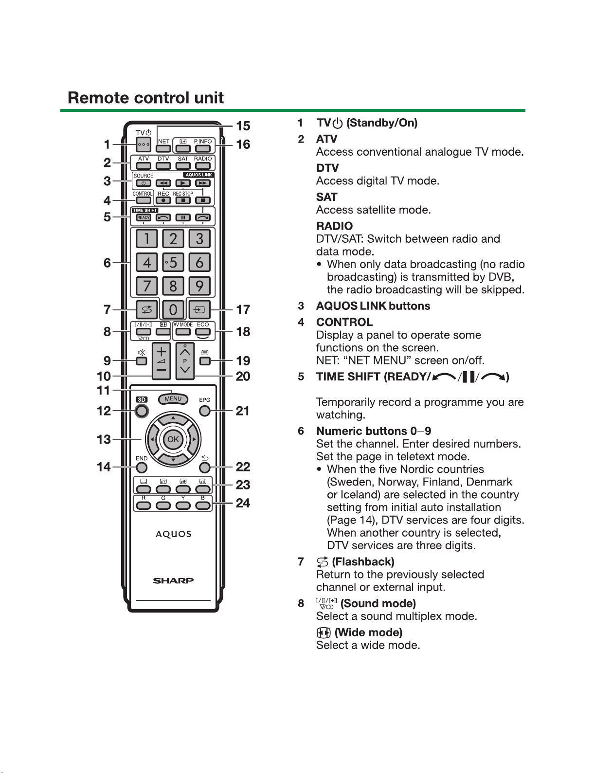
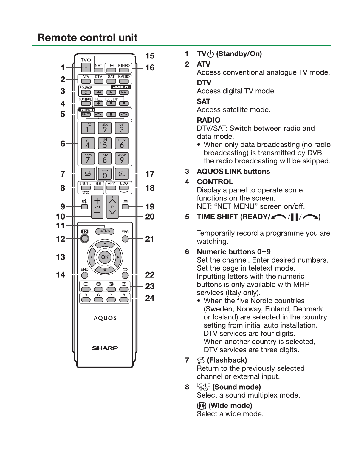
TopPage
LC-70LE835E/RU, 836E/S, 838E
SERVICE MANUAL
No. S12V570LE835E
LCD COLOUR TELEVISION
LC-70LE835E/RU
LC-70LE836E/S
MODELS
In the interests of user-safety (Required by safety regulations in some countries) the set should be restored to its original condition and only parts identical to those specified should be used.
LC-70LE838E
CONTENTS
SAFETY PRECAUTION
IMPORTANT SERVICE SAFETY PRE-
CAUTION ............................................................i
Precautions for using lead-free solder ...............ii
End of life disposal ............................................ iii
OUTLINE
MAJOR SERVICE PARTS ................................iv
CHAPTER 1. SPECIFICATIONS
[1] SPECIFICATIONS (LC-70LE835/836)........... 1-1
[2] SPECIFICATIONS (LC-70LE838).................. 1-2
CHAPTER 2. OPERATION MANUAL
[1] Parts Name .................................................... 2-1
[2] OPERATION MANUAL .................................. 2-7
CHAPTER 3. DIMENSIONS
[1] DIMENSIONS ................................................ 3-1
CHAPTER 5. ADJUSTMENT
[1] ADJUSTMENT PROCEDURE ......................5-1
CHAPTER 6. TROUBLESHOOTING TABLE
[1] TROUBLESHOOTING TABLE ......................6-1
[2] LED flashing specification at the time of the
error .............................................................6-18
CHAPTER 7. MAJOR IC INFORMATIONS
[1] MAJOR IC INFORMATIONS .........................7-1
CHAPTER 8. OVERALL WIRING/BLOCK DIAGRAM
[1] OVERALL WIRING DIAGRAM ......................8-1
[2] SYSTEM BLOCK DIAGRAM (LC-
70LE835E/RU, 838E) .................................... 8-2
[3] SYSTEM BLOCK DIAGRAM (LC-
70LE836E/S) .................................................8-3
Parts Guide
CHAPTER 4. REMOVING OF MAJOR PARTS
[1] REMOVING OF MAJOR PARTS ................... 4-1
[2] The location putting on the heat measure
sheet .............................................................. 4-7
[3] Precautions for assembly............................... 4-8
Parts marked with " " are important for maintaining the safety of the set. Be sure to replace these parts with specified ones for maintaining the
safety and performance of the set.
This document has been published to be used for
after sales service only.
The contents are subject to change without notice.
Page 2
LC-70LE835E/RU, 836E/S, 838E
LC70LE835E
SAFETY PRECAUTION
Service Manual
IMPORTANT SERVICE SAFETY PRECAUTION
Service work should be performed only by qualified service technicians who are thoroughly familiar with all safety checks and the
servicing guidelines which follow:
WARNING
1. For continued safety, no modification of any circuit should be
attempted.
2. Disconnect AC power before servicing.
CAUTION:
FOR CONTINUED PROTECTION AGAINST A
RISK OF FIRE REPLACE ONLY WITH SAME
TYPE FUSE.
• Use an AC voltmeter having with 5000 ohm per volt, or higher, sensitivity or measure the AC voltage drop across the resistor.
• Connect the resistor connection to all exposed metal parts having a
return to the chassis (antenna, metal cabinet, screw heads, knobs
and control shafts, escutcheon, etc.) and measure the AC voltage
drop across the resistor.
All checks must be repeated with the AC cord plug connection
reversed. (If necessary, a nonpolarized adaptor plug must be used
only for the purpose of completing these checks.)
Any reading of 1.05 V peak (this corresponds to 0.7 mA peak AC.)
or more is excessive and indicates a potential shock hazard which
must be corrected before returning the monitor to the owner.
F7001 (5A/250V)
DVM
BEFORE RETURNING THE RECEIVER
(Fire & Shock Hazard)
Before returning the receiver to the user, perform the following
safety checks:
3. Inspect all lead dress to make certain that leads are not pinched,
and check that hardware is not lodged between the chassis and
other metal parts in the receiver.
4. Inspect all protective devices such as non-metallic control knobs,
insulation materials, cabinet backs, adjustment and compartment
covers or shields, isolation resistor-capacitor networks, mechanical
insulators, etc.
5. To be sure that no shock hazard exists, check for leakage current
in the following manner.
• Plug the AC cord directly into a 220~240 volt AC outlet.
• Using two clip leads, connect a 1.5k ohm, 10 watt resistor paralleled by a 0.15µF capacitor in series with all exposed metal cabinet
parts and a known earth ground, such as electrical conduit or electrical ground connected to an earth ground.
///////////////////////////////////////////////////////////////////////////////////////////////////////////////////////////////////////////////////////////////////////////////////////////////////////////////////////////////////////////
TO EXPOSED
METAL PARTS
SAFETY NOTICE
Many electrical and mechanical parts in LCD color television have
special safety-related characteristics.
These characteristics are often not evident from visual inspection, nor
can protection afforded by them be necessarily increased by using
replacement components rated for higher voltage, wattage, etc.
Replacement parts which have these special safety characteristics are
identified in this manual; electrical components having such features
are identified by “ ” and shaded areas in the Replacement Parts
List and Schematic Diagrams.
///////////////////////////////////////////////////////////////////////////////////////////////////////////////////////////////////////////////////////////////////////////////////////////////////////////////////////////////////////////
For continued protection, replacement parts must be identical to those
used in the original circuit.
The use of a substitute replacement parts which do not have the same
safety characteristics as the factory recommended replacement parts
shown in this service manual, may create shock, fire or other hazards.
AC SCALE
1.5k ohm
10W
0.15µF
TEST PROBE
CONNECT TO
KNOWN EARTH
GROUND
i
Page 3
LC-70LE835E/RU, 836E/S, 838E
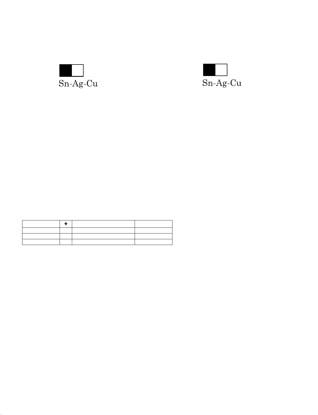
Precautions for using lead-free solder
Employing lead-free solder
• “PWBs” of this model employs lead-free solder. The LF symbol indicates lead-free solder, and is attached on the PWBs and service manuals. The
alphabetical character following LF shows the type of lead-free solder.
Example:
L Fa
Indicates lead-free solder of tin, silver and copper.
Indicates lead-free solder of tin, silver and copper.
L F a/a
Using lead-free wire solder
• When fixing the PWB soldered with the lead-free solder, apply lead-free wire solder. Repairing with conventional lead wire solder may cause damage or accident due to cracks.
As the melting point of lead-free solder (Sn-Ag-Cu) is higher than the lead wire solder by 40 °C, we recommend you to use a dedicated soldering
bit, if you are not familiar with how to obtain lead-free wire solder or soldering bit, contact our service station or service branch in your area.
Soldering
• As the melting point of lead-free solder (Sn-Ag-Cu) is about 220 °C which is higher than the conventional lead solder by 40 °C, and as it has poor
solder wettability, you may be apt to keep the soldering bit in contact with the PWB for extended period of time. However, Since the land may be
peeled off or the maximum heat-resistance temperature of parts may be exceeded, remove the bit from the PWB as soon as you confirm the
steady soldering condition.
Lead-free solder contains more tin, and the end of the soldering bit may be easily corroded. Make sure to turn on and off the power of the bit as
required.
If a different type of solder stays on the tip of the soldering bit, it is alloyed with lead-free solder. Clean the bit after every use of it.
When the tip of the soldering bit is blackened during use, file it with steel wool or fine sandpaper.
• Be careful when replacing parts with polarity indication on the PWB silk.
Lead-free wire solder for servicing
Part No. Description Code
ZHNDAi123250E J φ0.3mm 250g (1roll) BL
ZHNDAi126500E J φ0.6mm 500g (1roll) BK
ZHNDAi12801KE J φ1.0mm 1kg (1roll) BM
ii
Page 4

LC-70LE835E/RU, 836E/S, 838E
End of life disposal
End of life disposal
iii
Page 5
LC70LE835E
OUTLINE
Service Manual
MAJOR SERVICE PARTS
PWB Unit
Ref No. Parts No. Description
N DKEYDF733FM58 MAIN Unit (LC-70LE835E/RU) (*1)
N DKEYDF733FM59 MAIN Unit (LC-70LE836E/S) (*1)
N DKEYDF733FM60 MAIN Unit (LC-70LE838E) (*1)
N DUNTKF494FM02 R/C, OPC Unit
N DUNTKF770FM51 ICON Unit
N DUNTKF800FM52 KEY Unit
N RUNTKA819WJQZ 3D IR TRANSMITTER Unit
N RDENCA451WJQZ POWER Unit
N DUNTKF906FM55 LCD CONTROL Unit
N RUNTKA961WJZZ LED DRIVER Unit
NOTE: (*1) Replace MAIN PWB Unit (DKEYDF733FM**) in case of IC8401 or IC3303 failure.
OTHER Unit
Ref No. Parts No. Description
N R1LK695D3GW2AX 70" LCD Panel Module Unit (LK695D3GW2AX)
LC-70LE835E/RU, 836E/S, 838E
IC For Exclusive Use Of The Service
Ref No. Parts No. Description Q'ty
IC2001 RH-iXD241WJNJQ IC R5F21368CNFP (Monitor Microcomputer) 1
Service Jigs
Ref No. Parts No. Description Q'ty
N QCNW-L795WJQZ Main Unit to Power Unit (PD) 1
N QCNW-L519WJQZ POWER Unit to LED DRIVER Unit (LA) 1
N QCNW-L796WJQZ Main Unit to ICON Unit (CI) 1
N QCNW-K595WJQZ Main Unit to Speaker (SP) 1
N QCNW-G405WJQZ Main Unit to LCD Control Unit (PL) 1
N QCNW-F676WJQZ MAIN Unit to LCD CONTROL Unit (LW) 1
N QCNW-C222WJQZ LCD Control Unit to LCD Panel Unit, x2 2
iv
Page 6
LC-70LE835E/RU, 836E/S, 838E
LC70LE835E
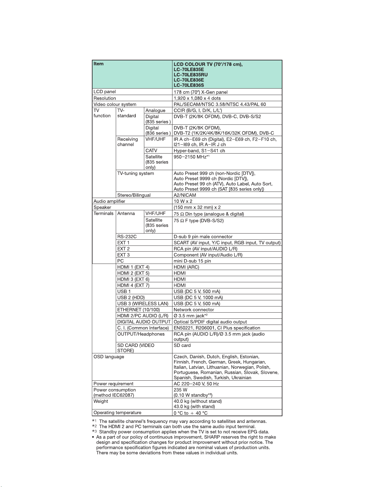
CHAPTER 1. SPECIFICATIONS
[1] SPECIFICATIONS (LC-70LE835/836)
Service Manual
1 – 1
Page 7
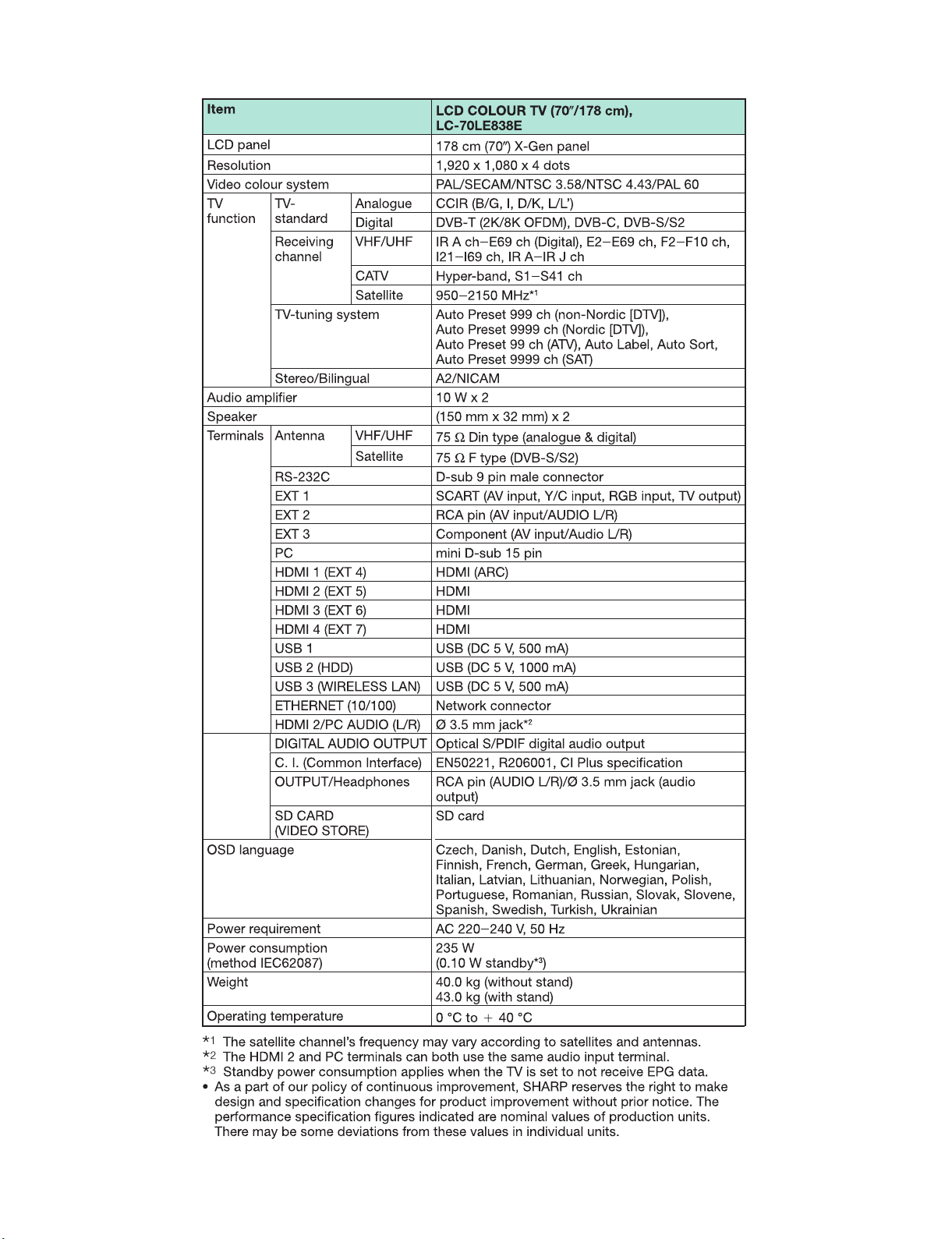
[2] SPECIFICATIONS (LC-70LE838)
LC-70LE835E/RU, 836E/S, 838E
1 – 2
Page 8
LC-70LE835E/RU, 836E/S, 838E
LC70LE835E
CHAPTER 2. OPERATION MANUAL
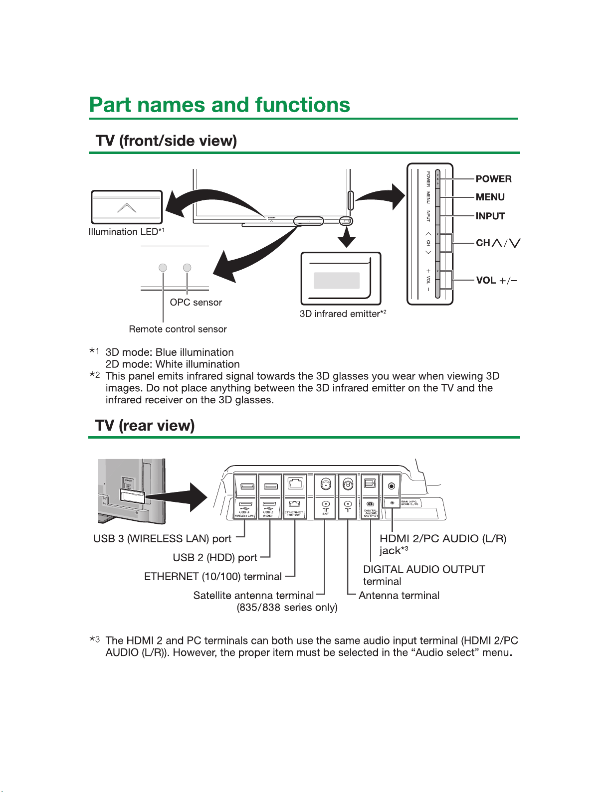
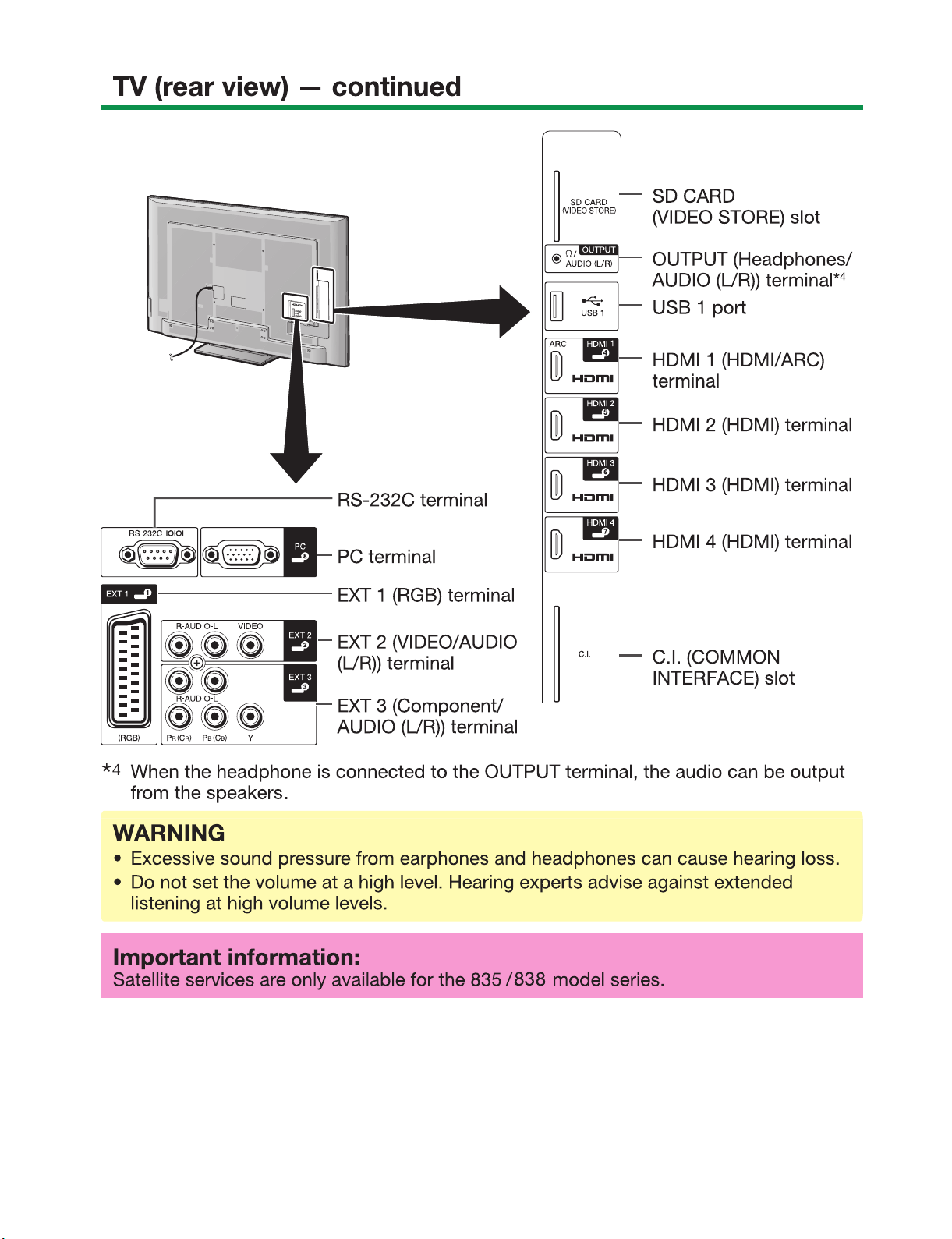
[1] Parts Name
Service Manual
2 – 1
Page 9
LC-70LE835E/RU, 836E/S, 838E
2 – 2
Page 10
LC-70LE835E/RU, 836E/S, 838E
• LC-70LE835E/RU,836E/S
2 – 3
Page 11
LC-70LE835E/RU, 836E/S, 838E
2 – 4
Page 12
LC-70LE835E/RU, 836E/S, 838E
• LC-70LE838E
2 – 5
Page 13
LC-70LE835E/RU, 836E/S, 838E
2 – 6
Page 14
LC-70LE835E/RU, 836E/S, 838E
[2] OPERATION MANUAL
2 – 7
Page 15
LC70LE835E
CHAPTER 3. DIMENSIONS
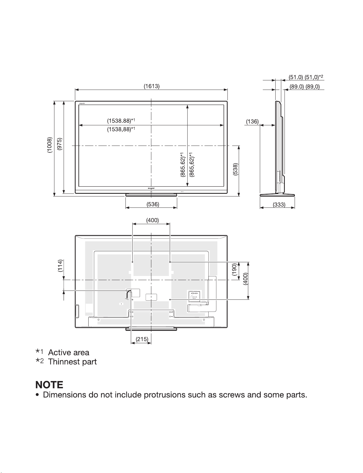
[1] DIMENSIONS
LC-70LE835E/RU, 836E/S, 838E
Service Manual
Unit: mm
3 – 1
Page 16
LC-70LE835E/RU, 836E/S, 838E
LC70LE835E
CHAPTER 4. REMOVING OF MAJOR PARTS
Service Manual
[1] REMOVING OF MAJOR PARTS
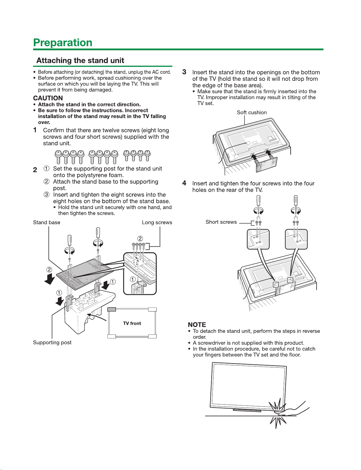
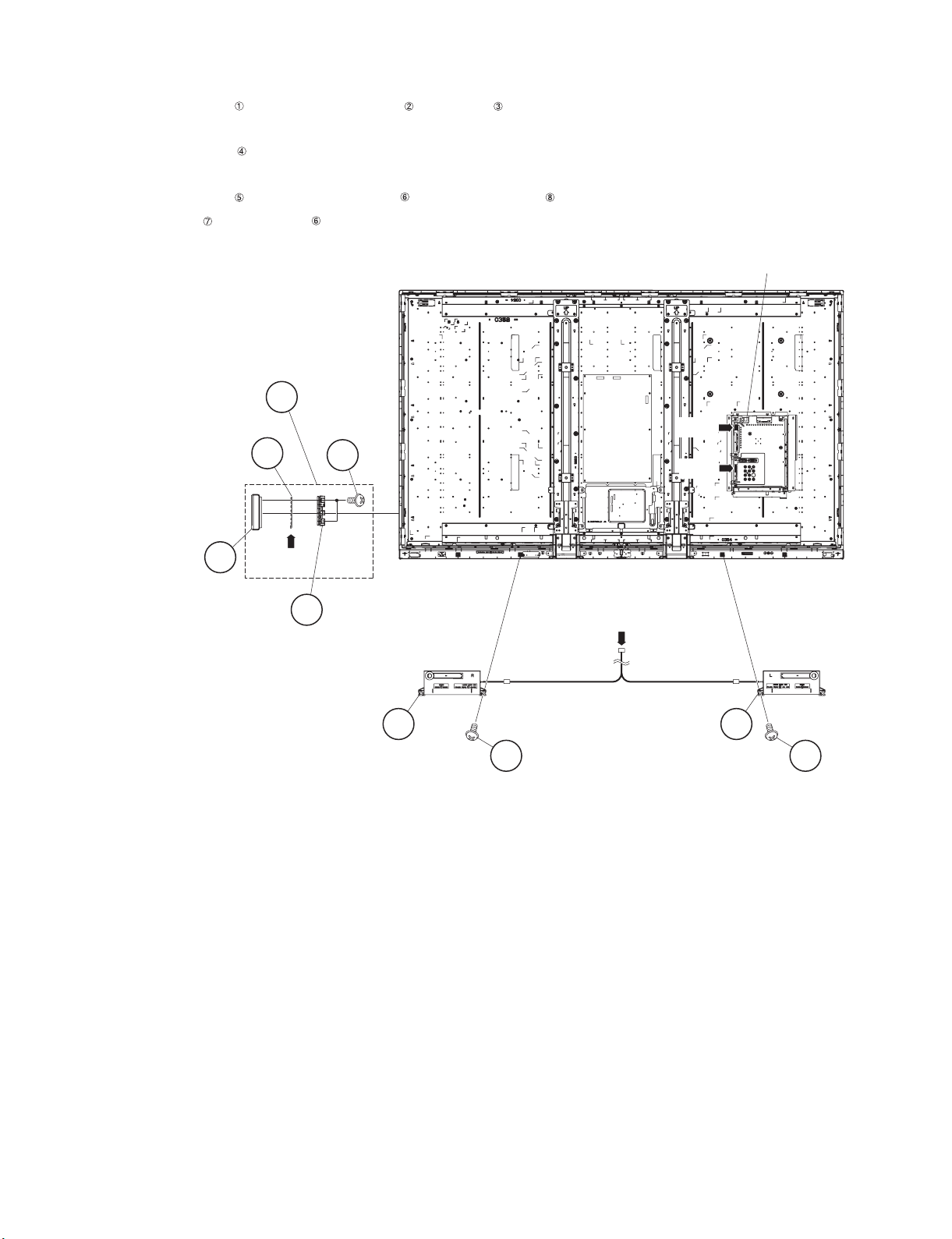
1. Removing of Stand Unit and Rear Cabinet Ass’y.
1. Remove the 4 lock screws and detach the Stand Unit .
2. Remove the 1 lock screw and detach the AC Cord Cover .
3. Disconnect AC wire and detach the AC Cord .
4. Remove the 4 VESA Hole Covers , 9 lock screws and 21 lock screws and detach the Rear Cabinet Ass’y .
3
VESA Hole Cover
2Stand Unit
4AC Cord Cover
5
AC Cord
[AC]
6
7
1
8
[AC]
Rear Cabinet Ass'y
9
[Precautions when mounting and removing the rear cabinet]
Basically, there is no problem as in LC-60LE632U. However, the screws on both sides are not tightened together with the Rear Cabinet Ass’y.
The inside is fixed by the module and Speaker.
Therefore, it does not come away completely, but only one side can come off.
Tighten together with the
Rear Cabinet Ass'y.
Fix with the 70" LCD Panel Module Unit.
Only one side (outer) can come off.
4 – 1
Page 17
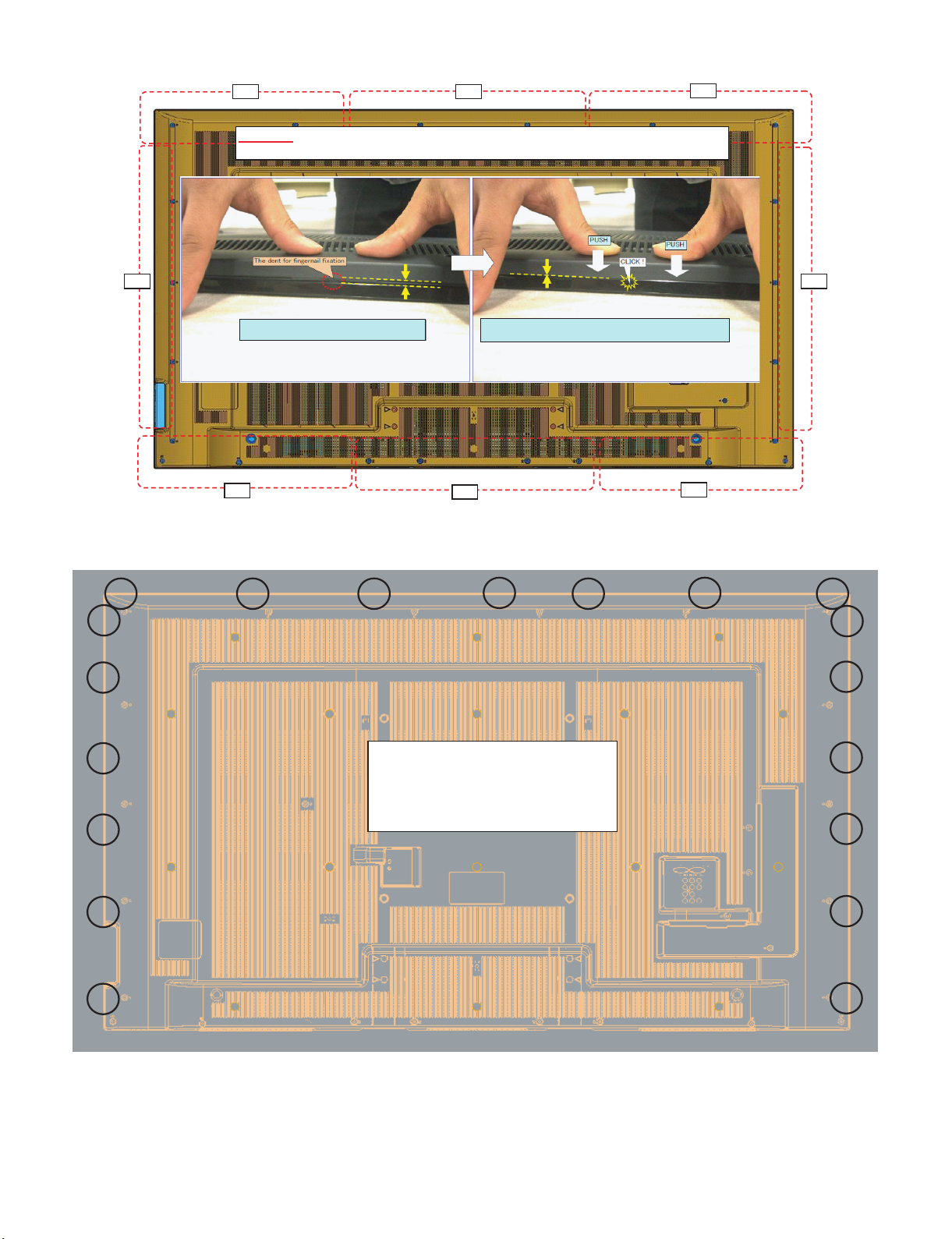
[Precautions for assembly]
Push
Push
Push
Push
Push
Push
Push
Push
CAUTION
Set it so that there may not be a clearance between Front Cabinet Ass'y and Rear Cabinet Ass'y.
19
places
LC-70LE835E/RU, 836E/S, 838E
There is a gap without the fingernail fitting
in completely only when covering with Rear Cabinet Ass'y.
(Front Cabinet Ass’y/Rear Cabinet Ass’y fingernail fixation place)
The fingernail is surely fixed when Rear cabinet Ass'y is
firmly pushed, and the gap disappears.
4 – 2
Page 18
LC-70LE835E/RU, 836E/S, 838E
2. Removing of Speaker (L/R) and KEY Unit.
1. Disconnect the SP wire.
2. Remove the 2 lock screws and detach the Speaker (L) , Speaker (R) .
3. Disconnect the RC wire.
4. Detach the KEY Unit Ass’y .
5. Disconnect the KM wire.
6. Remove the 2 lock screws and detach the Key Button from Key Button Cover .
7. Detach the KEY Unit from Key Button .
MAIN Unit
KEY Unit Ass'y
KEY Unit
Key Button
Cover
7
8
[KM]
Key Button
4
[SP]
5
[RC]
6
[SP]
2Speaker (L)3Speaker (R)
1 1
4 – 3
Page 19
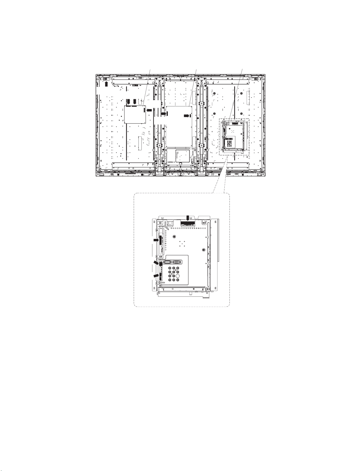
3. Removing of Connectors
1. Disconnect the following connectors from the MAIN Unit. (PD, LV, PL, Cl)
2. Disconnect the following connectors from the POWER Unit.(PD, LA)
3. Disconnect the following connectors from the LED DRIVER Unit. (L1, L2, LA)
LC-70LE835E/RU, 836E/S, 838E
LED DRIVER Unit
[L1/L2]
[L2]
[L1]
[LA]
[PD]
[LA]
MAIN Unit
MAIN UnitPOWER Unit
[PD]
[LV]
[PL]
[CI]
4 – 4
Page 20
LC-70LE835E/RU, 836E/S, 838E
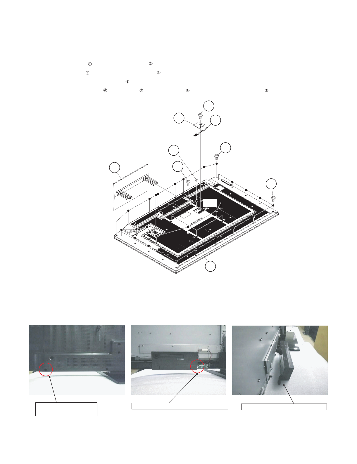
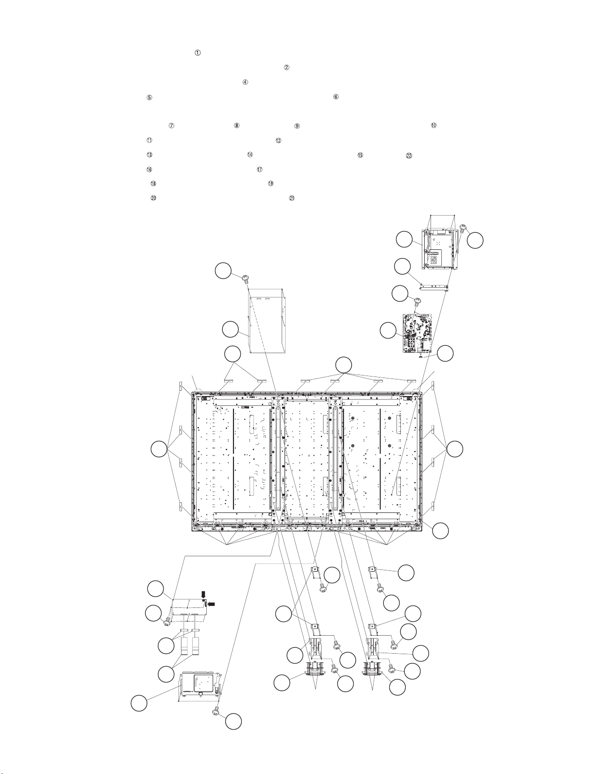
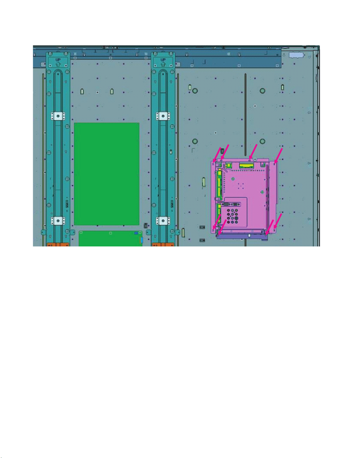
4. Removing of 70” LCD Panel Module Unit, LCD CONTROL Unit, MAIN Unit, POWER Unit.
1. Detach the 14 Fixing Metal Angle Ass’ys .
2. Remove the 12 Hooks and detach the 70” LCD Panel Module Unit .
3. Remove the 4 Hooks and detach the 2 Bottom Covers .
4. Remove the 4 lock screws and detach the Shield Ass’y (LCD CONTROL Unit) .
5. Disconnect the LW and PL wire.
6. Remove the 2 Connecting Cords , 2 Ferrite Cores , 6 lock screws and detach the LCD CONTROL Unit .
7. Remove the 5 lock screws and detach the Shield (MAIN Unit) .
8. Remove the 2 lock screws and detach the MAIN Unit and Terminal Angle (Bottom) and Spring .
9. Remove the 6 lock screws and detach the POWER Unit .
10.Remove the 12 lock screws and detach the 2 Stand Angles .
11.Remove the 16 lock screws and detach the 4 VESA Angle Ass’ys .
Fixing Metal Angle Ass'y
1Fixing Metal
Angle Ass'y
Hook
16
Shield (MAIN Unit)
12
11
15Terminal Angle
(Bottom)
13
17Power Unit
MAIN Unit
1
1
14
Fixing Metal
Angle Ass'y
22
Hook
Spring
1 Fixing Metal
Angle Ass'y
10LCD CONTROL
Unit
9
Shield Ass'y
6
(LCD CONTROL Unit)
2
70" LCD Panel
Module Unit
VESA
Angle Ass'y
Angle
Hook
Hook
21
VESA
Angle Ass'y
20
21
20
19 Stand
18
4 Bottom Cover
Hook
20
[PL]
[LW]
VESA
21
Angle Ass'y
8Ferrite Core
19Stand
7Connecting Cord
Angle
Bottom
Cover
4
Hook
20
18
5
4 – 5
Page 21
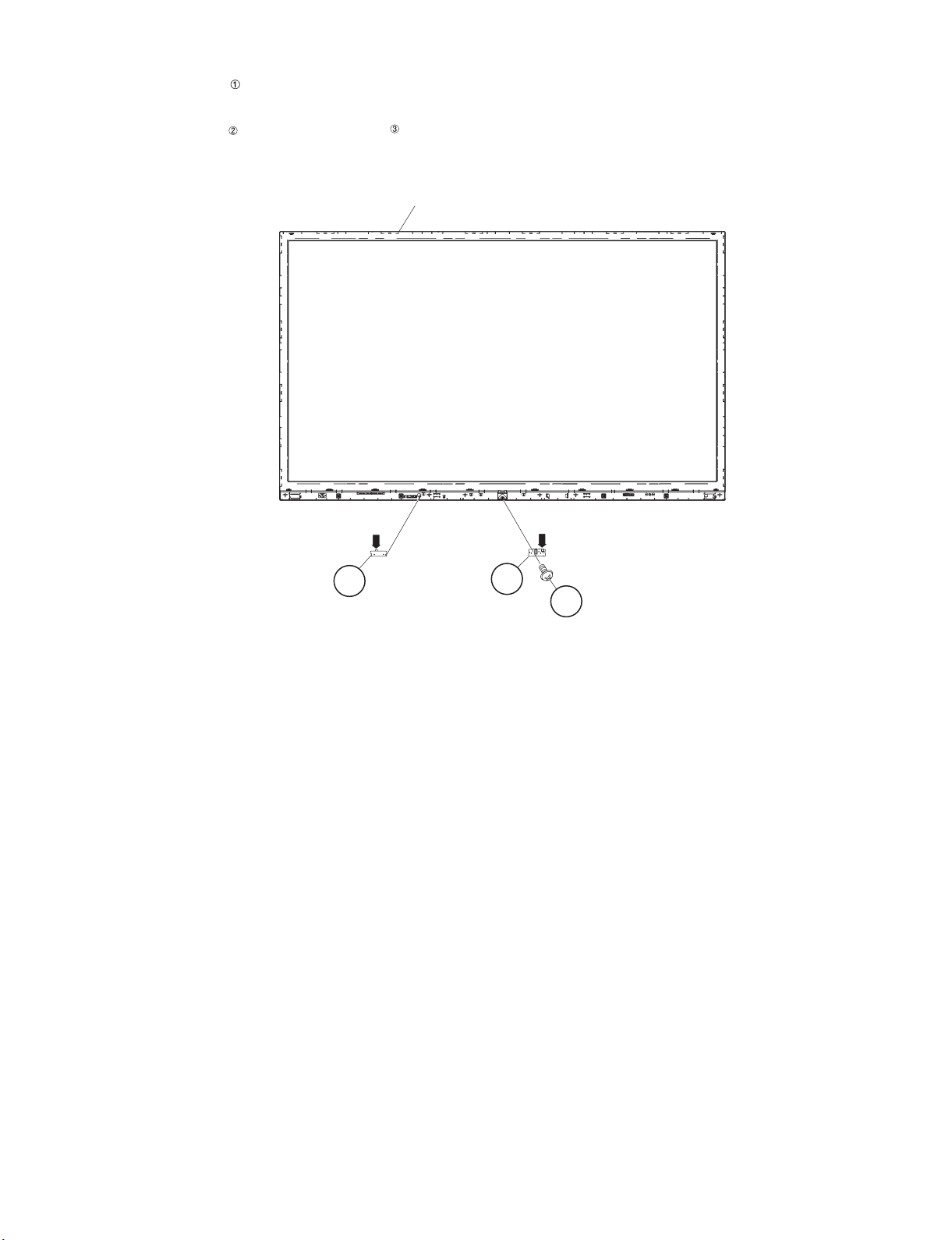
5. Removing of R/C OPC Unit, ICON Unit, WiFi Unit.
1. Detach the R/C OPC Unit .
2. Disconnect the RC wire.
3. Remove the 1 lock screw and detach the ICON Unit .
4. Disconnect the CI wire.
Front Cabinet Ass'y
LC-70LE835E/RU, 836E/S, 838E
1R/C OPC Unit
[RC]
[CI]
3ICON Unit
2
4 – 6
Page 22
LC-70LE835E/RU, 836E/S, 838E
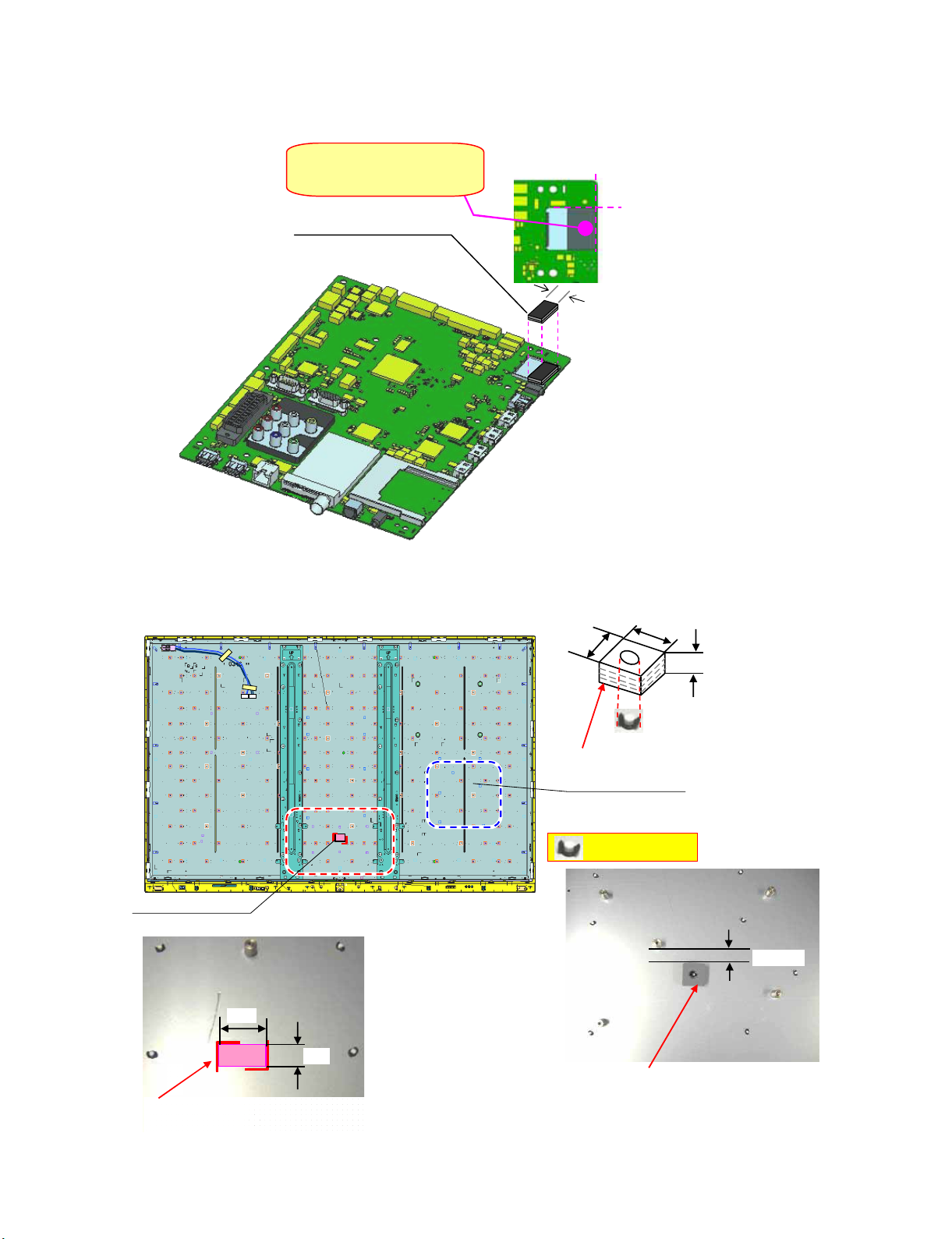
[2] The location putting on the heat measure sheet
1. MAIN PWB Unit
2. BACK LIGHT CHASSIS
ATTENTION
Do not push strongly.
(Transformation prevention of holder)
PSPAGA963WJZZ
SPACER
Base = Card holder edge
Over to the right side is NG.
Base =
Base =
Card holder edge
Card holder edge
15mm side
PSPAZC782WJKZ
C-PWB Cooler
25
15
Stick the sheet along carved line.
(COOLING-SHEET sticks to IC5801. )
20
Sticky side is a panel side.
PSPAZC850WJKZ
MAIN Cooling Sheet
Don't push.(panel holder)
Stick the COOLING-SHEET to panel holder
(COOLING-SHEET sticks to IC3303. )
20
11
4 – 7
Page 23
LC-70LE835E/RU, 836E/S, 838E
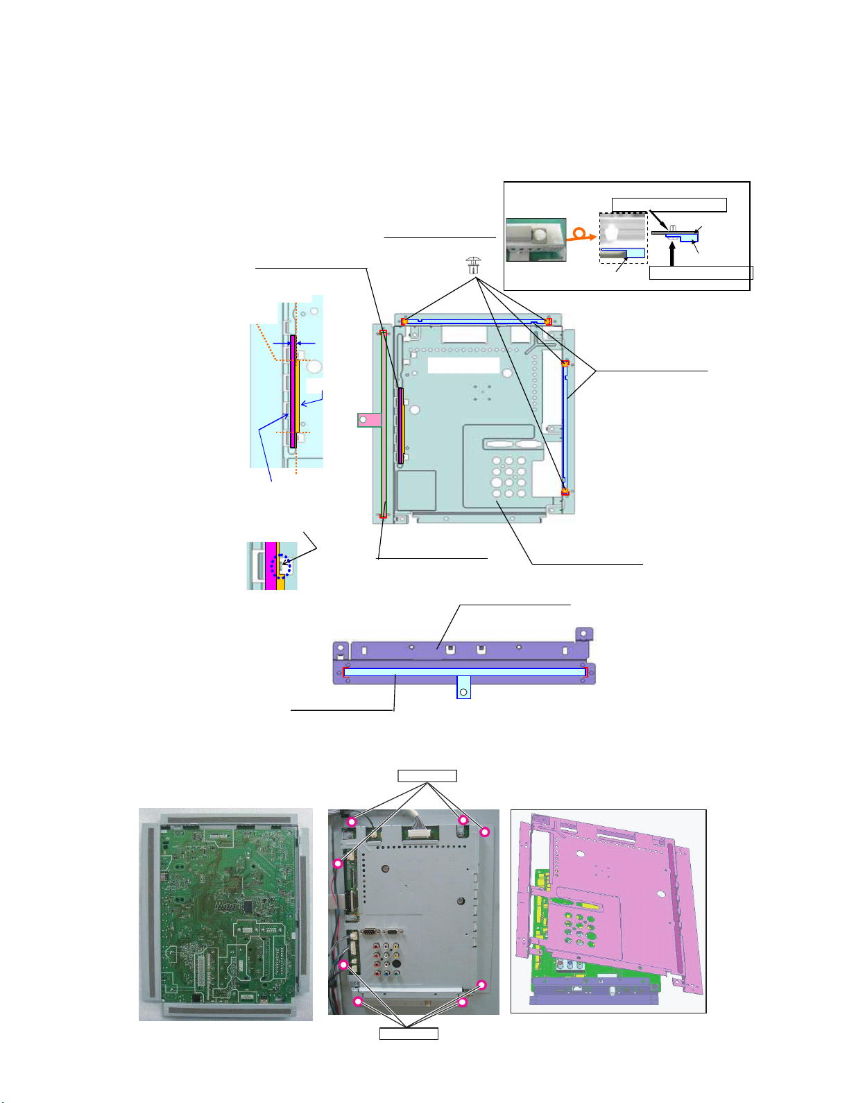
[3] Precautions for assembly
1. Points to be checked and precautions when servicing the unit
Mount the main PWB Ass’y on the backlight chassis and check that the EMI-prevention parts are not peeled and twisted from the access holes. (The
EMI-prevention parts, conductive nonwoven fabric gaskets, must be seen from the access holes.)
[Countermeasure]
Attach the conductive nonwoven fabric gaskets on the shielded case on the main PWB.
WH is to be locked securely.
MAIN SHIELD
GASKET short
Base = Bend line
Base = Cut line
(Fit to edge)
PMLT-A676WJZZ
GASCKET
5mm
PCLICA004WJKZ
for GASKET
Turn
GASKET short
Insert from the back side.
Tape side
Gascket
side
Stick guscket so as not to
overlap with the bend area. (x2)
PMLT-A695WJZZ
GASKET
State where the main PWB and shielded case are assembled
PMLT-A694WJZZ
GASKET
Rear side view
Rear side view
PSLDMB751WJFW
SHIELD (MAIN Umit)
LANGKD148WJFW (LC-70LE835E/RU,838E)
LANGKD192WJFW (LC-70LE836E/S)
TERMINAL ANGLE (Bottom)
PMLT-A693WJZZ
GASKET
Access hole
Access hole
4 – 8
Page 24
LC-70LE835E/RU, 836E/S, 838E
The following is a drawing mounting the main PWB Ass’y on the backlight chassis. (The parts indicated by -> are the access holes for confirmation.)
(Main PWB Ass’y => State where the shielded case and RF terminal angle are mounted on the main PWB)
4 – 9
Page 25

LC-70LE835E/RU, 836E/S, 838E
LC70LE835E
CHAPTER 5. ADJUSTMENT
Service Manual
[1] ADJUSTMENT PROCEDURE
1. Adjustment method after PWB and/or IC replacement due to repair
The unit is set to the optimum at the time of shipment from the factory.
If any value should become improper or any adjustment is necessary due to the part replacement, make an adjustment according to the following procedure.
1. Procure the following units in order to replace the main unit.
MAIN UNIT: DKEYDF733FM58 (LC-70LE835E,RU)
MAIN UNIT: DKEYDF733FM59 (LC-70LE836E,S)
MAIN UNIT: DKEYDF733FM60 (LC-70LE838E)
NOTE: [Caution when replacing IC (IC2001) in the main unit]
The above IC are Monitor microcomputer.
Before replacing the relevant part, procure the following parts in which the data have been rewritten.
IC2001 RH-iXD241WJNJQ Monitor microcomputer
NOTE: [Caution when replacing ICs (IC8401, IC3303) in the main unit]
When replacing either IC8401 or IC3303, exchange MAIN units for DKEYDF733FM58 (LC-70LE835E,RU), DKEYDF733FM59 (LC70LE836E,S) DKEYDF733FM60 (LC-70LE838E) .
Each part should not be individually exchanged.
NOTE: HDMI ROM Writing
After replacing IC1504, execute “HDMI EDID WRITE” on the page 5/21.
Please execute it after checking MODEL NAME & INCH SIZE. are correct.
If MODEL NAME & INCH SIZE. are not correct, set them previously. (Refer to 2.)
The ROM data based on information of MODEL NAME & INCH SIZE.
1) Enter the process adjustment mode in TV.
2) Use the cursor keys ( / ) and CH keys ( / ) of R/C to select the item [HDMI EDID WRITE] on the page 5/21.
3) It is completed with OK displayed.
2. After replacing the LCD panel or LCD control/MAIN UNIT, check MODEL NAME in the following procedure.
1) Enter the process adjustment mode in TV.
2) Use the cursor keys ( / ) and CH keys ( / ) of R/C to select the item [MODEL NAME] on the page 21/21.
3) Verify that the Model name is displayed.
4) If the Model name doesn’t match, select the values of the Model name with the VOL keys (+/-).
5) After selection in Step 4), press the OK key, and it is completed with OK displayed.
6) Use the cursor keys ( / ) and CH keys ( / ) of R/C to select the item [PANEL_SIZE] on the page 21/21.
7) Verify that the panel size is displayed.
8) If the size doesn’t match, select the values of the panel size with the VOL keys (+/-).
9) After selection in Step 8), press the OK key, and it is completed with OK displayed.
10)After setting [MODEL NAME] [PANEL_SIZE], unplug the AC power cord and plug it back in.
3. After replacing the LCD panel or LCD control PWB, adjust the VCOM in the following procedure.
1) Enter the process adjustment mode.
2) Use the cursor keys ( / ) and CH keys ( / ) of R/C to select the item [VCOM ADJ] on the page 10/21.
3) Press the OK key to verify that the adjustment pattern is displayed.
4) Use VOL keys (+/-) of R/C to adjust the flicker in the center of the screen to minimum.
5) When the optimal state is achieved in Step 4), press the OK key to turn the pattern to OFF.
5 – 1
Page 26
LC-70LE835E/RU, 836E/S, 838E
2. Entering and exiting the adjustment process mode
1) Unplug the AC power cord of running TV set to force off the power.
2) While holding down the “VOL (-)” and “INPUT” keys on the set at once, plug in the AC power cord to turn on the power.
The letter “K” appears on the screen. This state is in Inspection mode.
3) Next, hold down the “VOL (-)” and “CH ( )” keys on the set at once.
Multiple lines of blue characters appearing on the screen indicate that the set is now in the adjustment Process mode.
If you fail to enter the adjustment process mode (the display is the same as normal startup), retry the procedure.
4) To exit the adjustment process mode after the adjustment is done, unplug the AC power cord to force off the power.
(When the power is turned off with the remote controller, once unplug the AC power cord and plug it in again. In this case, wait for 20 seconds or
so after unplugging.)
CAUTION: Use due care in handling the information described here lest the users should know how to enter the adjustment process mode.
If the settings are tampered with in this mode, unrecoverable system damage may result.
3. Remote controller key operation and description of display in adjustment process mode
1. Key operation
Remote controller key Main unit key Remote controller key Main unit key Function
CH keys ( / ) CH ( / )
VOL keys (+/-) VOL (+/-) Changing a selected item setting (+1/-1)
Cursor ( / )
Cursor ( / )
INPUT INPUT Input source switching (toggle switching) (TV→EXT1→ etc...)
OK — Executing a function
RETURN — Returning to a present page
— Turning a page (PREVIOUS/NEXT)
— Changing a selected line setting (+10/-10)
Moving an item (line) by one (UP/DOWN)
Input mode is switched automatically when relevant adjustment is started so far as the necessary input signal is available.
5 – 2
Page 27
4. Description of display
(1) Present˴page / number of total pages (4) Inducing display
(3) Present colour system
(2) Input that has been selected now (5) Inch setting and Model name display
1/21 INPUT1 AUTO EURO
LC-70LE835E/RU, 836E/S, 838E
MAIN Version
BOOT Version
Monitor Version
T-CON Version/LED CON Version
NET TV KEY/MAC
CI+INFO/SECURE BOOT
FRC Version
TOUCH SENSOR/IR Micom Version
LAMP ERROR
MONITOR ERR CAUSE
1.00 (E 2011/**/** )
xxxxxxx
xxxxxxx
xxxxxxxx/xxxx
xxxxxxx
xxxxx/YES
xxxxxxx
xxxxxxx
0
1)xxxxxx 2)xxxxxx
3)xxxxxx 4)xxxxxx
NORMAL STANDBY CAUSE
ERROR STANDBY CAUSE
(6) Item name (7) Parameter
No. Description Display specification
(1) Present page/number of total pages 2char/2char Decimal Number mark.
(2) Input that has been selected now TUNER/DTV/INPUT1/INPUT2/INPUT3/INPUT5/INPUT6/INPUT7/etc. ⋅⋅⋅
(3) Present colour system AUTO/N358/N443/PAL/SECAM/480i/580i/1080i/50 etc. ⋅⋅⋅
(4) Inducing display EUROPE/RUSSIA/SWEDEN
(5) Inch setting and Model name display Inch setting and Model name display
(6) Item name Max. 30 char
(7) Parameter Max. 60 char
0
0000
5 – 3
Page 28
LC-70LE835E/RU, 836E/S, 838E
5. List of adjustment process mode menu
The character string in brackets [ ] will appear as a page title in the adjustment process menu header.
Page Line Item Description Remarks (adjustment detail, etc.)
1/21 [INFO]
1 MAIN Version 1xxx (xxxxx) Main software version
2 BOOT Version xxxxxxx BOOT Version.
3 Monitor Version xxxxxxx Monitor software version
4 T-CON Version/LED CON Version xxxxxxxx/xxxx T-CON/LED CON Version
5 NET TV KEY/MAC xxxxxxx NET TV KEY/MAC Address
6 CI+INFO/SECURE BOOT xxxxx/YES CI+ Key Information/SECURE BOOT
7 MARLIN xxxxxxx
8 FRC Version xxxxxxx
9 IR Micom Version xxxxxxx
10 LAMP ERROR 0 Number of termination due to lamp error.
11 MONITOR ERR CAUSE 1)xxxxxx 2)xxxxxx
3)xxxxxx 4)xxxxxx
12 NORMAL STANDBY CAUSE 0 Situation that became standby at the end. (Excluding the error)
13 ERROR STANDBY CAUSE 0 0 0 0 Error standby cause
2/21 [INIT]
1 INDUSTRY INIT Enter Initialization to factory settings execution.
2 INDUSTRY INIT (-Public) OFF Initialization to factory settings execution. (Public mode is excluded)
3 PUBLIC MODE OFF Public mode ON/OFF setting
4 Center Acutime — Main operating hours.
5 RESET OFF Main operating hours reset.
6 Backlight Acutime — Backlight operating hours.
7 RESET OFF Backlight operating hours reset.
8 LAMP ERROR RESET OFF Lamp error reset.
9 ADJ PARAM SET Enter ADJ PARAM SET
10 VIC XPOS 0 X-coordinate setting for VIC READ
11 VIC YPOS 0 Y-coordinate setting for VIC READ
12 VIC SIGNAL TYPE MAIN Signal type setting for VIC READ
13 VIC READ OFF Picture level acquisition function
3/21 [TUNER ADJ]
1 TUNER ADJ Enter TUNER auto adjustment execution
2 PAL+TUNER ADJ Enter PAL TUNER auto adjustment execution
3 TUNER ADJ (SMPTE) Enter TUNER auto adjustment execution (SMPTE)
4 PAL+TUNER ADJ (SMPTE) Enter PAL TUNER auto adjustment execution (SMPTE)
5 TUNER ADJ (SMPTE CH57) Enter TUNER auto adjustment execution (SMPTE CH57)
6 PAL+TUNER ADJ (SMPTE CH57) Enter PAL TUNER auto adjustment execution (SMPTE CH57)
7 TUNER CONTRAST A_GAIN 14 TUNER signal level adjustment
8 TUNER CONTRAST D_GAIN 2048 TUNER signal level adjustment
9 TUNER CONTRAST OFFSET 256 TUNER signal level adjustment
4/21 [PAL MAIN]
1 PAL ADJ Enter PAL adjustment
2 SECAM ADJ Enter SECAM adjustment
3 N358 ADJ Enter N358 adjustment
4 PAL CONTRAST A_GAIN 14 PAL contrast adjustment
5 PAL CONTRAST D_GAIN 2048 PAL contrast adjustment
6 PAL CONTRAST OFFSET 256 PAL contrast adjustment
7 SECAM CONTRAST A_GAIN 14 SECAM contrast adjustment
8 SECAM CONTRAST D_GAIN 2048 SECAM contrast adjustment
9 SECAM CONTRAST OFFSET 256 SECAM contrast adjustment
10 N358 CONTRAST A_GAIN 14 N358 contrast adjustment
11 N358 CONTRAST D_GAIN 2048 N358 contrast adjustment
12 N358 CONTRAST OFFSET 256 N358 contrast adjustment
5/21 [CEC TEST]
1 HDMI CEC TEST Enter HDMI CEC test
2 HDMI EDID WRITE Enter HDMI EDID WRITING
3 INSPECT USB TERM Enter Reading inspection of USB memory terminal
4 MONIDATA READ [TEMP/OPC] OFF MONITOR Temperature/OPC Acquisition tool.
5 SD CARD TEST Enter SD CARD TEST
6 CAUSE RESET Enter Reset of standby cause
Last error standby cause.
(Level appears in green on the upper right)
5 – 4
Page 29
LC-70LE835E/RU, 836E/S, 838E
Page Line Item Description Remarks (adjustment detail, etc.)
6/21 [COMP15KMAIN]
1 COMP15K ALL ADJ Enter Component 15K picture level adjustment
2 COMP15K MAIN Y GAIN 140 Y GAIN adjustment value
3 COMP15K MAIN CB GAIN 150 Cb GAIN adjustment value
4 COMP15K MAIN CR GAIN 150 Cr GAIN adjustment value
5 COMP15K Y OFFSET 64 Y OFFSET adjustment value
6 COMP15K CB OFFSET 128 Cb OFFSET adjustment value
7 COMP15K CR OFFSET 128 Cr OFFSET adjustment value
7/21 [HDTV]
1 HDTV ADJ Enter HDTV video level adjustment
2 HDTV Y GAIN 140 HDTV Y GAIN adjustment value
3 HDTV CB GAIN 150 HDTV Cb adjustment value
4 HDTV CR GAIN 150 HDTV Cr adjustment value
5 HDTV Y OFFSET 64 HDTV Y OFFSET adjustment value
6 HDTV CB OFFSET 128 HDTV Cb OFFSET adjustment value
7 HDTV CR OFFSET 128 HDTV Cr OFFSET adjustment value
8/21 [ANALOG PC]
1 ANALOG PC ADJ Enter DVI ANALOG video level adjustment
2 R OFFSET 64 R CUTOFF adjustment value
3 G OFFSET 64 G CUTOFF adjustment value
4 B OFFSET 64 B CUTOFF adjustment value
5 R GAIN 44 R DRIVE adjustment value
6 G GAIN 44 G DRIVE adjustment value
7 B GAIN 44 B DRIVE adjustment value
9/21 [SCART]
1 SCART RGB ADJ Enter SCART RGB level adjustment
2 SCART RGB ADJ (FASTSW) Enter SCART RGB ADJ (FASTSW) adjustment
3 SCART R CUTOFF 64 SCART R CUTOFF adjustment value
4 SCART G CUTOFF 64 SCART G CUTOFF adjustment value
5 SCART B CUTOFF 64 SCART B CUTOFF adjustment value
6 SCART R GAIN 44 SCART R GAIN adjustment value
7 SCART G GAIN 44 SCART G GAIN adjustment value
8 SCART B GAIN 44 SCART B GAIN adjustment value
10/21 [LUMAADJ]
1 VCOM ADJ 64 Common bias adjustment (2D)
11/21 [LEV]
1 R GAIN (LO) 0 R DRIVE adjustment value
2 G GAIN (LO) 0 G DRIVE adjustment value
3 B GAIN (LO) 0 B DRIVE adjustment value
4 R GAIN (HI) 0 R DRIVE adjustment value
5 G GAIN (HI) 0 G DRIVE adjustment value
6 B GAIN (HI) 0 B DRIVE adjustment value
12/21 [M EEP SET]
1 MONITOR TIME OUT ON Monitor and the main communication time-out setting
2 MONITOR MAX TEMP 59 MONITOR MAX temperature setting
3 MONITOR EEP READ/WRITE WRITE MONITOR EEPROM READ/WRITE Setting/execution
4 MONITOR EEP ADR 0x 0 MONITOR EEPROM arbitrary addressing
5 MONITOR EEP DATA 0x 0 MONITOR EEPROM arbitrary data specification
13/21 [M TEST PATTERN]
1 LCD TEST PATTERN Pattern with built-in LCD controller display
2 LCD TEST PATTERN1 NOT SUPPORT
3 LCD TEST PATTERN2 OFF
4 LCD TEST PATTERN3 NOT SUPPORT
5 LCD TEST PATTERN4 NOT SUPPORT
14/21
1 TCON Version EXT.1 xxxxx
2 TCON Version EXT.2
3 TCON Version EXT.3
4 TCON Version EXT.4
15/21
1 3DHDMI FPGA Version xxxxx
22D→3D FPGA Version xxxxx
3 3D LED BRIGHTNESS xxxxx
4 3D IR EMITTER CONTROL xxxxx
5 – 5
Page 30
LC-70LE835E/RU, 836E/S, 838E
Page Line Item Description Remarks (adjustment detail, etc.)
16/21 [FR REGI]
1 CROSSTALK ADJ MODE Enter
2 CROSSTALK TH1
3 CROSSTALK TH2
4 CROSSTALK TH3
5 CROSSTALK TH4
6 CROSSTALK GAIN1
7 CROSSTALK GAIN2
8 CROSSTALK GAIN3
17/21
1 WiFi SSID 2.4GHz xxxxx
2 WiFi SSID 5 GHz xxxxx
3 WiFi RSSI 2.4GHz xxxxx
4 WiFi RSSI 5 GHz xxxxx
5 WiFi TIME 5 GHz xxxxx
6 WiFi RSSI TEST xxxxx
7 WiFi RSSI RESULT xxxxx
18/21
1 READ/WRITE READ Read/Write
2 SLAVE/ADDRESS SLAVE0 Slave address
3 REGISTER ADDRESS 0x 0
0x 0
4 WRITE DATA 0x 0
0x 0
5 READ DATA 0x 0
0x 0
19/21
1 RF AGC BG 6 RF-AGC BG adjustment execution
2 RF AGC DK 5 RF-AGC DKG adjustment execution
3 RF AGC I 6 RF-AGC I adjustment execution
4 RF AGC L/L’ 4 RF-AGC L/L’ adjustment execution
20/21 [ETC]
1 ERROR STANDBY CAUSE1 NO RECORD ERROR STANDBY CAUSE
2 ERROR STANDBY CAUSE2 NO RECORD
3 ERROR STANDBY CAUSE3 NO RECORD
4 ERROR STANDBY CAUSE4 NO RECORD
5 ERROR STANDBY CAUSE5 NO RECORD
6 STANDBY CAUSE RESET OFF Reset stand by cause.
21/21 [ETC]
1 EEP SAVE OFF Writing setting values to EEPROM.
2 EEP RECOVER OFF Reading setting values from EEPROM.
3 MONITOR ERROR CAUSE RESET OFF Reset of monitor error cause
4 MODEL NAME LE835E MODEL NAME
5 PANEL SIZE 70 Panel size setting.
6 VERUP FLAG ENABLE Enter Verup Flag
7 PANEL LIMIT ON PANEL LIMIT
8 PANEL RANGE LIMIT xxx PANEL RANGE LIMIT
9 SHORT CHECK MODE Enter Check LED Back light
10 SHORT CHECK CURRENT 60
11 CURRENT SW LOW
12 PRODUCT EEP ADR 0x 0 Don’t touch when serving (for producer of factory)
13 PRODUCT EEP DATA 0x 0 Don’t touch when serving (for producer of factory)
14 PRODUCT FACTORY 1 Don’t touch when serving (for producer of factory)
Register address
Writing data
Reading data
5 – 6
Page 31

6. Special features
1. NORMAL STANDBY CAUSE (Page 1/21)
Display of a cause (code) of the last standby.
The cause of the last standby is recorded in EEPROM whenever it is possible.
Checking this code will be useful in finding a problem when you repair the troubled set.
2. EEP SAVE (Page 21/21)
Storage of EEP adjustment value.
3. EEP RECOVER (Page 21/21)
Retrieval of EEP adjustment value from storage area.
4. MONITOR ERR CAUSE (Page 1/21)
Display of a cause (code) of Error from Monitor microcomputer.
The cause of Error is recorded in EEPROM whenever it is possible.
Checking this code will be useful in finding a problem when you repair the troubled set.
1) This displays Error code and time when the error occurred.
The latest error is displayed on “1)”.
The error that happens ahead of “1)” is displayed on “2)”.
2) The character depends on the way how to acquire Time Information.
T: Time is acquired from digital broadcasting
This doesn’t contain “Time offset” which is considered a time difference and Daylight-Saving Time, etc. ...
U: Time is acquired from analog broadcasting (teletext)
B: Accumulation time of Backlight
In the case that Time information cannot be acquired, “B” is displayed.
LC-70LE835E/RU, 836E/S, 838E
Example) In this example, it is shown that the error occurred 3 times.
1) 16 T07/01/01 12:03 Error code: 16 (lamp error) Time: 07/01/01 12:03
* It is latest Error.
* Time is acquired from digital broadcasting.
* Time is UTC which doesn't have Time offset.
2) 16 U01/01/01 04:07 Error code: 16 (lamp error) Time: 07/01/01 04:07
* It is Error that happens ahead of “1)”.
* Time is acquired from analogue broadcasting.
3) 16 B00000004:11 Error code: 16 (lamp error) Accumulation time: It is displayed that 4:11 have passed after Backlight driving.
* It is Error that happens ahead of “2)”.
4) 00 0000000000000 No error (“00” shows that the error is not occurred.)
5 – 7
Page 32

LC-70LE835E/RU, 836E/S, 838E
7. Lamp Error detection
1. Function
This LCD color TV set incorporates a Lamp error detection feature that automatically turns off the power for safety under abnormal lamp or lamp
circuit conditions. If by any chance anything is wrong with the lamp or lamp circuit or if the lamp error detection feature is activated for some reason, the following will result.
1) The power is interrupted in about 500ms after it is turned on.
(A central icon on the front of the TV flash on and off.: ON for 400ms and OFF for 1600ms.)
2) If the above phenomenon 1) occurs 5 times, it becomes impossible to turn on the power.
(A central icon keep flashing on/off.)
2. Measures
1) Set the lamp error detection to OFF
Enter the adjustment process mode, referring to “2. Entering and exiting the adjustment process mode”.
The adjustment process mode can ignore “5 times count”, so If the above phenomenon 1) occurs 1~4 times, the lamp will go out.
If Lamp Error detection pin [4pin of PD: P9602/19pin of IC2001] is “High” by a trouble with the lamp and lamp circuit, it can boot-up by the
adjustment process mode.
Please execute “Lamp Error detection off-mode”
Unplug the AC power cord of running TV set to force off the power.
While holding down the “VOL (-)” and “CH ( )” keys on the set at once, plug in the AC power cord to turn on the power.
After a central icon flash off, separate the fingers from key on the set.
Then, you can check the operation to see if the lamp and lamp circuit are in trouble.
If you fail boot-up, retry the procedure.
2) Resetting the lamp error count
After the lamp and lamp circuit are improved from a trouble, reset the lamp error count.
(Because the power cannot be turned on, if a lamp error is detected 5 consecutive times.)
a) Enter the adjustment process mode, referring to “2. Entering and exiting the adjustment process mode”.
b) Using the cursor ( / ) key, move to the cursor to [LAMP ERROR RESET], Line 8 on adjustment process mode service page 2/21.
c) With the cursor ( / ) keys, select the [LAMP ERROR RESET] value.
Finally press the cursor (OK)., the count is reset.
Check LAMP ERROR Count on adjustment process mode Page 2/21.
Table of contents of adjustment process mode Page 2/21
INDUSTRY INIT Enter
INDUSTRY INIT (-Publicl) OFF
Pubric MODE OFF
Center Acutime
RESET OFF
Backlight Acutime
RESET OFF
LAMP ERROR RESET OFF
Resetting to "0"
ADJ PARAM SET Enter
VIC XPOS
VIC YPOS
0
0
VIC SIGNAL TYPE MAIN
VIC READ OFF
5 – 8
Page 33

LC-70LE835E/RU, 836E/S, 838E
8. Public Mode
1. Starting the Public Mode
1) Method of needing password
a) While holding down the “INPUT” and “Volume UP” keys on the set at once, plug in the AC power cord to turn on the power.
b) Display the Pass Word input screen.
After a while, value of Enter password appears on the screen.
Enter password
Enter password
Enter password
Operation procedure
• The initial input position is the digit at the left end.
• For the numeric keys “0” to “9” of R/C, key input is accepted.
Input of the other keys is prohibited.
• Change “—” to “ ” by inputting the numeric key at the input position, and shift the input position rightward one digit.
• When three digits are completely input, the Pass Word is judged.
c) Check the Pass Word by inputting three digits.
If the Pass Word “0” “2” “7”, it shifts to the PUBLIC Mode setting screen.
In another case, the screen is erased, and it operates in the ordinary mode.
2. Exiting the Public Mode Setting screen
• There are two following ways to exit the Public Mode setting screen.
1) Turn off the power.
2) Select “Execution” in the PUBLIC_Mode to execute it.
Activate the restart under the set content.
Here, the START input SOURCE setting is excluded since this item is referred to only when the power is turned on.
3. Set value of the Public Mode
• When the shipment setting is done, a set each value in Public Mode is initialized.
(PUBLIC MODE in the process mode Setting of a flag is also initialized)
• Separately, the shipment beginnings when all except for each set value in Public Mode is initialized are provided for a process mode.
(INDUSTRY INIT (-Public))
• Only when turning on the PUBLIC MODE item, each setting is effective.
• After it decides it with EXECUTE, it AC OFF/ON it to reflect a set value.
4. Basic operation in the Public Mode
Vol (+/-) or Cursor ( / ) Change or execution of the set value.
CH (+/-) or Cursor ( / ) Movement to the selected item.
Decision (ok) Excution (Used by the items "Execution" and "RESET".)
Public Mode setting screen.
Public Mode
POWER ON FIXED
SHUT DOWN MODE
MAXIMUM VOLUME
VOLUME FIXED
VOLUME FIXED LEVEL
RC BUTTON
PANEL BUTTON
MENU BUTTON
AV POSITION FIXED
ON SCREEN DISPLAY
INPUT MODE START
INPUT MODE FIXED
LOUD SPEAKER
RC PATH THROUGH
232C POWON
PUBLIC MODE
RESET
EXECUTE
5 – 9
[VARIABLE]
[NORMAL]
[60]
[VARIABLE]
[20]
[RESPOND]
[RESPOND]
[RESPOND]
[VARIABLE]
[YES]
[NORMAL]
[VARIABLE]
[ON]
[OFF]
[DISABLE]
[ON]
Page 34

LC-70LE835E/RU, 836E/S, 838E
5. Operation after “RESET”
Select “RESET” in the PUBLIC Mode, and it operates as follows when it is executed (refer to the basic operation).
• The set contents in the PUBLIC mode are initialized.
• It does not exit the PUBLIC mode.
• If “EXCUTE” is not executed, the content that does RESET is not reflected.
6. Setting items. (* Item names and selective items are expressed in English.)
1) Power ON fixed [POWER ON FIXED]
Option “VARIABLE”, “FIXED_ALL”, “FIXED_BODYKEY” or “RCRESPOND” (loop enabled)
Default “VARIABLE”
Function • VARIABLE
• FIXED_ALL
• FIXED_BODYKEY
• RC RESPOND
Key disabled when set
other than default
Remarks • When selecting to “FIXED_ALL”, function related standby factors (see below) doesn’t work. and not selecting.
If the power button is pressed in the ordinary mode in setting to “FIXED_ALL” and “FIXED_BODYKEY”, the caution is displayed for 5 seconds.
• OFF TIMER (SLEEP) (*Only when setting to FIXED_ALL)
OFF TIMER (Sleep)
No operation OFF
No signal OFF (including the power management)
* These items does not exist according to the model.
: “POWER/RECEPTION” key on TV unit or remote control is enabled.
: “POWER/RECEPTION” key on TV unit or remote control is disabled.
: Only the “MAIN POWER” key on TV unit is disabled (The remote control is enabled).
: The main unit’s POWER switch toggles between ON and Standby (the same operation by the
remote control).
When power button on the main unit is pressed When power button on R/C is pressed
No Power off by power button.
* The OSD display is an example.
If another ODS is previously displayed, the status is reset (MENU or similar).
2) Instantaneous current shutdown setting in turning off the power [SHUT DOWN MODE]
Option “NORMAL” or “QUICK”
Default NORMAL
Function • This function decides whether scanning digital tuner is enabled or disabled when the power is standby.
NORMAL
QUICK
Remarks In selecting “QUICK”, the function does not work for the following items. (selection impossible.)
• ON TIMER, QUICK START, DIGITAL FIXED, etc.
* These items does not exist according to the model.
3) Volume maximum level [MAXIMUM VOLUME]
: Scanning digital tuner is enabled when the power is standby.
: Scanning digital tuner is disable.
It is possible to put into the standby state instantaneously due to power off input, when the
power is standby.
Immediately, state is a complete standby.
No Power off by remote control.
Option 0~60 (loop disabled)
Default 60
Function The volume cannot be increased more than the adjusted value (the main unit’s speaker only).
Remarks • When setting to 59 or less, only the figure is displayed in the normal mode; the volume bar is not displayed.
• The volume of the headphones is limited.
• The setting is impossible when VOLUME FIXED is set to FIXED.
5 – 10
Page 35

LC-70LE835E/RU, 836E/S, 838E
4) Volume fixed [VOLUME FIXED]
Option “VARIABLE”, “FIXED”, “ACCTRL” or “AC/RCCTRL” (loop enabled)
Default “VARIABLE”
Function • VARIABLE
• FIXED
• AC CTRL
• AC/RC CTRL
Exception • In the adjustment process, the volume can be set to any level regardless of this setting.
Disabled key when
setting to FIXED
Remarks • [MAXIMUM VOLUME] has priority to [VOLUME FIXED]
5) Volume fixed level [VOLUME FIXED LEVEL]
Option 0~60 (loop disabled)
Default 20
Function The volume is fixed to the adjusted value (the main unit’s speaker only).
Exception • In the adjustment process, the volume can be set to any level regardless of this setting.
Remarks • When [VOLUME FIXED] is set to “VARIABLE”, the setting cannot be changed.
• VOLUME UP/DOWN [both remote control and main unit]
•MUTE
* Main units's key is enabled for operating menu.
* When setting to FIXED, Maximum volume is fixed.
• The volume of the headphones is fixed.
• When setting to “FIXED”, the volume is not displayed in operating Disabled key.
• In menu operation, the main unit’s keys (Vol (+/-)) are enabled.
• Volume level graphic be omitted to volume level number.
• In setting to FIXED, ONVOL of On TIMER is not selected (Eliminate Item)
• In setting to AC/RC CTRL, ONVOL of On TIMER i is not selected (Eliminate Item)
• VOLUME can be abbreviated to VOL.
: The volume is not fixed.
: The volume is fixed to the value adjusted in the volume fixed level.
: The unit starts at the volume specified in the volume fixed level, when power is turned on in the
case of the AC-ON only.
: The unit starts at the volume specified in the volume fixed level, when power is turned on in
any case.
(AC→ON, remote control→ON, main utit's key→ON)
6) Remote control operation [RC BUTTON]
Option “RESPOND”, “NORESPOND” or “LIMITED” (loop enabled)
Default “RESPOND”
Function The operation of the remote control’s keys is set.
RESPOND
NO RESPOND
LIMITED
Exception • All the keys are enabled regardless of this setting while entering the adjustment process mode, inspection mode or
Public Mode setting screen.
Remarks The enable keys when setting to “LIMITED” are depended on Model.
7) Main Unit Operation [PANEL BUTTON]
Option “RESPOND” or “NO RESPOND” (loop enabled)
Default “RESPOND”
Function • RESPOND
• NO RESPOND
Exception • The start operation in the adjustment process mode, inspection mode are enabled regardless of this setting.
• All the keys are enabled regardless of this setting while entering the adjustment process mode, inspection mode or
Public Mode setting screen.
• For the models with the MENU key on the main unit, menu operation is possible regardless of the setting during the
initial setting when the power is turned on for the first time.
: The remote control’s keys in the normal state are enabled.
: The remote control’s keys in the normal state are disabled.
The POWER key (RECEPTION/STANDBY key) is also disabled.
: Only a part of keys (CHANNEL, etc.) is enabled and other keys are disabled.
: The main unit’s keys are enabled.
: The main unit’s keys are disabled excluding the POWER key (RECEPTION/STANDBY key).
5 – 11
Page 36

LC-70LE835E/RU, 836E/S, 838E
8) Menu operation [MENU BUTTON]
Option “RESPOND” or “NO RESPOND” (loop enabled)
Default “RESPOND”
Function The MENU key on the main unit and remote control is decided whether it is enabled or disabled.
Exception • RESPOND
Disabled key excluding
Menu key when setting
to not default
Remarks When setting to “NO RESPOND”
9) AV position fixed [AV POSITION FIXED]
Option “VARIABLE” or “FIXED” (loop enabled)
Default “VARIABLE”
Function • VARIABLE
Remarks • When receiving the sound select direct keys (AV POSITION key, OPC, DOLBY key, etc.), only the actual state is
• NO RESPOND
All the direct transition keys to menu display. (AUTO PRESET, MANUAL MEMORY and others)
* These keys does not exist according to the model.
• For the models with the MENU key on the main unit, menu operation is possible regardless of the setting while the
initial setting when the power is turned on for the first time.
• FIXED
displayed; no setting is changed.
* These keys does not exist according to the model.
• The settings for the Public mode are retained after the personal data is initialized, each item for the AV position and
image/sound adjustment are not initialized.
: The manu key is enabled.
: The manu key is disabled.
: All the keys are enabled regardless of this setting while entering the process mode, inspection
mode or Public Mode setting screen.
: AV position is not fixed.
: AV position is fixed.
: The image/sound adjustment items in the menu are fixed in the selected state.
: When receiving “AV POSITION” of the remote control, only the actual state is displayed, and
setting is not changed.
10) OSD display [ON SCREEN DISPLAY]
Option “YES”, “NO” or “LIMITED” (loop enabled)
Default “YES”
Function • YES
Key which may be
enabled
(Example of the confusing key)
Disabled key when
setting to not default
Remarks • When setting to “NO”,
“LIMITED” is looped only in case of need (destination).
: OSD is displayed.
•NO
•LIMITED
• It is OK in the case that simple input select occur or the original state returns soon automatically.
• When setting to “NO”, the keys which is related to visibility of the screen and sound cannot be used.
STILL IMAGE, SCREEN DISPLAY, OFF TIMER, AV POSITION, BRIGHTNESS SENSOR, SCREEN SIZE SELECT,
AUTO PRESET, MANUAL MEMORY, IMAGE SELECT, SOUND SELECT, LANGUAGE, Closed caution
* Disabled keys dependeds on the models.
ON TIMER (Watching reservation) is cleared.
OFF TIMER “SLEEP” is cleared.
* These items does not exist according to the model.
• When setting to “NO”,
These Displays (Version-up, Public mode setting screen, Pass Word input screen of Public
Mode, the adjustment process mode, K mark of inspection mode) are enabled regardless of
this setting.
: The following OSD is not displayed.
Registration, setting, adjustment menu, channel call, volume bar, and input select.
: Only a part of OSD (CH call: “New Information” etc...) is not displayed.
5 – 12
Page 37

LC-70LE835E/RU, 836E/S, 838E
11) Start mode [INPUT MODE START]
Option “NORMAL” or “Input source 1 (input selection or channel)” ... (loop enabled)
Default “NORMAL”
Function Which kinds of input source or channel is decided when the power turning on.
NORMAL : The content of the last memory is followed.
Remarks • When setting to not Normal, ON TIMER (Watching reservation) has priority.
• When setting to “NORMAL”, [INPUT MODE FIXED] is set to “VARIABLE” and [INPUT MODE FIXED] is prohibited to
select. (selection impossible.)
Example of option: “NORMAL”, “TVD (002TV)”, “INPUT1”, “INPUT2”, “INPUT3”, “HDMI1”, “HDMI2”, “HDMI3”, “HDMI4”.
12) Input fixed [INPUT MODE FIXED]
Option “VARIABLE”, “FIXED”, “ACCTRL” or “AC/RCCTRL” (loop enabled)
Default VARIABLE
Function VARIABLE
Disabled key when
setting to “FIXED”
Remarks • If [INPUT MODE START] is Normal, this function cannot be set.
FIXED
AC CTRL
AC/RC CTRL
CHANNEL (+/-), DIRECT CHANNEL buttons, FLASHBACK, INPUT SELECT, TV/VIDEO, AUTO PRESET,
MANUAL MEMORY, i.LINK, DIRECTINPUTSELECT, ATV, DTV, EPG, RADIO etc...
Set to “VARIABLE” automatically.
• When setting to “FIXED”,
The item related to the channel setting and input selection in Menu are not displayed.
ON TIMER (Watching reservation) is not active.
* These items does not exist according to the model.
: If [INPUT MODE START] is set to Normal, input mode is not fixed.
: When “INPUT MODESTART” is active, it is impossible to switch to another channel or input
source.
: When “INPUT MODESTART” is active the unit starts at the input mode which is selected when
power is turned on in the case of the AC-ON only.
: When “INPUT MODESTART” is active the unit starts at the input mode which is selected
when power is turned on in any case.
(AC→ON, remote control→ON, main utit's key→ON)
13) Speaker ON/OFF selection [LOUD SPEAKER]
Option “ON” or “OFF” (loop enabled)
Default ON
Function ON
OFF
Remarks • When the VOL (+/-) key is pressed, the mute icon is displayed for 4 seconds.
• For the MUTE key and sound-related keys, caution is displayed.
• For the headphones, normal operation is possible.
14) Remote control path through [RC PATH THROUGH]
Option “OFF”, “ON: TVRCE” or “ON: TVRCD” (loop enabled)
Default OFF
Function The item decide whether the signal received by the remote control’s light-receiving section is output to the blankpin (9pin)
of RS232C.
OFF
ON: TVRCE
ON: TVRCD
Exception • In the case of “ON: TV RCD”, the start operation in the adjustment process mode, inspection mod are enabled
regardless of this setting.
• In the case of “ON: TV RCD”, all the keys are enabled regardless of this setting while entering the adjustment process
mode, inspection mode or Public mode setting screen.
Remarks * Remote control path through does not exist according to the model.
: The sound from the speakers is output.
: The sound from the speakers is not output even if the headphones are not used.
: This function is not active.
: This function is active, and remote control is active, too.
: This function is active, but remote control is not active.
5 – 13
Page 38

LC-70LE835E/RU, 836E/S, 838E
15) 232C power ON control [232C POWON]
Option “ENABLE” or “DISABLE” (loop enabled)
Default DISABLE
Function The item decide whether Power ON by the 232C command is enabled/disabled in the standby state.
The same function as 232C command “RSPW”.
ENABLE
DISABLE
16) Public mode setting [PUBLIC MODE]
Option “OFF” or “ON” (loop enabled)
Default OFF
Function The item decide whether Public mode setting menu are enabled or disabled.
The same item as [PUBLIC MODE] in the adjustment process menu.
OFF
ON
Remarks Each operation of the Public mode is impossible unless this item is set to ON.
9. Copy Mode
1. Starting the Copy Mode
1) Method of needing password
a) While holding down the “INPUT” and “Volume UP” keys on the set at once, plug in the AC power cord to turn on the power.
b) Display the Pass Word input screen.
After a while, value of Enter password appears on the screen.
: POWR0001 is always enabled.
: Start-up may be impossible at POWR0001.
(If the 232C command reception module is set to OFF, the command is invalid.)
: Public mode is not active.
: Public mode is active.
Enter password
Operation procedure
• The initial input position is the digit at the left end.
• For the numeric keys “0” to “9” of R/C, key input is accepted.
Input of the other keys is prohibited.
• Change “—” to “ ” by inputting the numeric key at the input position, and shift the input position rightward one digit.
• When three digits are completely input, the Pass Word is judged.
c) Check the Pass Word by inputting three digits.
If the Pass Word “3” “6” “9”, it shifts to the Copy Mode setting screen.
In another case, the screen is erased, and it operates in the ordinary mode.
2. Exiting the Copy Mode Setting screen
There is following way to exit the Copy Mode setting screen.
• Turn off the power. (Unplug the AC power cord from the outlet to forcibly turn off the power.)
3. Basic operation in the Copy Mode
CH (+/-) or Cursor ( / )
Decision (ok) Execution
Movement to the selected item.
Enter password
Enter password
5 – 14
Page 39

4. Restriction of Copy Mode
• USB thumb drive should be more than 1Mbyte.
• File system of USB thumb drive should be FAT (FAT32).
• More than one USB thumb drive shouldn't be connected to TV.
• All USB terminals can be valid, but more than one USB thumb drive shouldn't be connected to TV.
• If USB device is detected by TV, focus is not appropriated to items.
• In Copy mode (TV→USB) and (USB→TV), following should be mutched.
Vender Name (Fixed)
Key Information (Fixed)
USB Cline Version
Inch Size
Country setting (Factory initialization)
Model Name
Software Version
• In each TV, setup of Network and IP control should be set again.
NOTE: • It is unnecessary to execute “Initial Auto Instration” for Copy Mode.
(Obviously, setting the country is also unnecessary.)
• Copy Mode can’t start until the TV recognizes a USB device.
TV takes about 20 seconds to recognizes a USB device after boot-up.
5. Copy data
Copy data is as follows;
LC-70LE835E/RU, 836E/S, 838E
Copy Data Remarks
Size of Ch call
Card slot selection Setting
Alphabet sorts do/not
HOME/Store Setting
Public Setting
Sound multiplex information in each Ch
Administrative information for Time Shift Vendor ID, Product ID, Serial ID for storage
Communication's information IP address, Gateway, DNS address
Kinds of Security key encryption (WiFi)
Access point identifier (WiFi)
Key for access point
IP control setting information Device name, Login ID, Password, Communication port
DTV service list Number of all services
CH list
Number of broadcasting on each network
Last value Last network information (DVB-T, DVB-S, DVB-C, ATV)
Last channel information
Volume, wide mode, and subtitle
Local Time Information Information that corrects ±X time against Universal Time
User Manu Data User Menu Data don't have these information.
Temporary data
Message list, Reception report, EPG, Off timer, Off video, and Signal strength
Peculiarity data for TV
DRM information for DivX, Mac address, and Accumulated time information
Connected equipment information
(But the recorder selection of the AQUOS LINK setting can be copied.)
physical address
Category of equipment
Maker Name
Connected model name
Data related to encrypted broadcasting (CI+)
Adjustment process mode Data
5 – 15
Page 40

LC-70LE835E/RU, 836E/S, 838E
Copy mode
TV USB [Start ]
USB TV [Start ]
Copy mode
Copy mode
Copy mode
Execcute
Success
Fail
Execcute
Success
Fail
Copy mode
Copy mode
Copy mode
Copy mode
TV USB [Wait... ]
USB TV [Start ]
TV USB [Done ]
TV USB [Failed ]
USB TV [Start ]
TV USB [Start ]
USB TV [Wait... ]
USB TV [Done ]
USB TV [Failed ]
USB TV [Start ]
USB TV [Start ]
TV USB [Start ]
TV USB [Start ]
TV USB [Start ]
6. Operating
1) Copy mode (TVψUSB))
Execute start in Copy Mode setting screen.
If USB device is detected by TV,
focus is not appropriated to items.
[Wait] is displayed while executing it.
When succeeding: Done is displayed.
When failing: Failed is displayed.
Key opration is not valid in coping.
After success of copy,
unplug the AC power cord from the outlet, please.
2) Copy mode (USBψTV))
Execute start in Copy Mode setting screen.
If USB device is detected by TV,
focus is not appropriated to items.
[Wait] is displayed while executing it.
When succeeding: Done is displayed
When failing: Failed is displayed.
Key opration is not valid in coping.
After success of copy,
unplug the AC power cord from the outlet, please.
5 – 16
Page 41

10. Video signal adjustment procedure
[VIDEO input signal]
100% white Black
[VIDEO input signal]
100% white Black
The adjustment process mode menu is listed in Section 5.
Signal generator level adjustment check. (Adjustment to the specified level)
• Composite signal PAL : 0.7Vp-p ± 0.02Vp-p (Pedestal to white level)
• 33K component signal (50 Hz) : Y level : 0.7Vp-p ± 0.02Vp-p (Pedestal to white level)
: PB, PR level : 0.7Vp-p ± 0.02Vp-p
• ANALOG PC (RGB) signal : RGB level : 0.7Vp-p ± 0.02Vp-p
10.1. Entering the adjustment process mode
Enter the adjustment process mode according to Section 2.
10.2. PAL signal adjustment
Adjustment point Adjustment conditions Adjustment procedure
1 Setting [Signal]
PAL
Full field colour bar
composite signal
[Terminal]
EXT1 SCART Video (PAL)
IN
• Feed the PAL full field colour bar signal (75% colour saturation) to EXT1
SCART IN.
LC-70LE835E/RU, 836E/S, 838E
2 Auto adjustment
performance
* ATTENTION: Please execute [10.3. TUNER adjustment] afterwards if you adjust [10.2. PAL signal adjustment] after all adjustments are
completed.
Adjustment process
[PAL ADJ] page 4/21
Bring the cursor on [PAL ADJ] and press [OK].
[PAL ADJ OK] appears when finished.
10.3. TUNER adjustment
Adjustment point Adjustment conditions Adjustment procedure
1 Setting [Signal]
PAL sprit field colour Bar
RF signal UV
[Terminal]
TUNER
• Feed the PAL Split Field colour bar signal (E-12ch) to TUNER.
• Make sure the PAL colour bar pattern has the sync level of 7:3 with the picture
level.
Signal level: 55 dB µV ± 1dB (75Ω LOAD)
[E-12CH]
χ100% white
2 Auto adjustment
performance
Adjustment process
[TUNER ADJ] page 3/21
Bring the cursor on [TUNER ADJ] and press [OK].
[TUNER ADJ OK] appears when finished.
10.4. SECAM adjustment
Adjustment point Adjustment conditions Adjustment procedure
1 Setting [Signal]
2 Auto adjustment
performance
SECAM
Full field colour Bar Signal
[Terminal]
EXT1 SCART IN
Adjustment process
[SECAM ADJ] page 4/21
• Feed the SECAM full field colour bar signal (75% colour saturation) to EXT1
SCART IN.
Bring the cursor on [SECAM ADJ] and press [OK].
[SECAM ADJ OK] appears when finished.
5 – 17
Page 42

LC-70LE835E/RU, 836E/S, 838E
100% white Black
100% white Black
100% white Black
100% white Black
10.5. ADC adjustment (Component 15K)
Adjustment point Adjustment conditions Adjustment procedure
1 Setting [Signal]
COMP15K, 50Hz
100% Full field colour bar
Signal
[Terminal]
EXT3 COMPONENT IN
• Feed the COMPONENT 15K 100% full field colour bar signal (100% colour
saturation) to EXT3 COMPONENT IN.
2 Auto adjustment
performance
Adjustment process
[COMP15k ALL ADJ]
page 6/21
10.6. ADC adjustment (Component 33K)
Adjustment point Adjustment conditions Adjustment procedure
1 Setting [Signal]
COMP33K, 50Hz
100% Full field colour bar
Signal
[Terminal]
EXT3 COMPONENT IN
2 Auto adjustment
performance
Adjustment process
[HDTV ADJ] page 7/21
10.7. PC signal adjustment (ANALOG D-Sub 15pin)
Adjustment point Adjustment conditions Adjustment procedure
1 Setting [Signal]
XGA, 60Hz
100% Full Field Colour Bar
Signal
Bring the cursor on [COMP15k ALL ADJ] and press [OK].
[COMP15K ALL ADJ OK] appears when finished.
• Feed the COMPONENT 33K 100% full field colour bar signal (100% colour saturation) to EXT3 COMPONENT IN.
Bring the cursor on [HDTV ADJ] and press [OK].
[HDTV ADJ OK] appears when finished.
• Feed the XGA 60Hz 100% full field colour bar signal (100% colour saturation)
to PC IN.
[Terminal]
PC IN
2 Auto adjustment
performance
Adjustment process
[ANALOG PC ADJ] menu
page 8/21
10.8. RGB (SCART) adjustment (RGB 15K)
Adjustment point Adjustment conditions Adjustment procedure
1 Setting [Signal]
2 Auto adjustment
performance
RGB 15K, 50Hz
100% Full field colour bar
signal
[Terminal]
EXT1 SCART RGB IN
Adjustment process
[SCART RGB ADJ] menu
page 9/21
Bring the cursor on [ANALOG PC ADJ] and press [OK].
[ANALOG PC ADJ OK] appears when finished.
• Feed the RGB 15k 50Hz 100% full field colour bar signal (100% colour saturation) to EXT1 SCART IN.
Bring the cursor on [SCART RGB ADJ] and press [OK].
[SCART RGB ADJ OK] appears when finished.
5 – 18
Page 43

LC-70LE835E/RU, 836E/S, 838E
11. White balance adjustment
For white balance adjustment, adjust the offset values on pages 11/21.
[Condition of the unit for inspection] : Modulated light (+16)
AV MODE: DYNAMIC
Active Backlight: OFF
OPC: OFF
Asing Time: Min, 60 minute
[Input signal condition] : HDMI 1080i 15IRE (LO), 78IRE (HI)
[Adjustment reference device] : Minolta CA-210
[Adjustment procedure]
1) Display the current adjustment status at R/G/B_GAIN (HI). (Page 11/21 of process adjustment)
The signal of 78IRE is input.
2) Read the value of the luminance meter. x=0.272, y =0.277
3) Change R_GAIN (HI)/ B_GAIN (HI) (Adjustment offset value) on page 11/21 of process adjustment so that the values of the luminance meter
approach x=0.272 and y =0.277.
(Basically, G is not changed. If adjustment fails with R and B, change G. When G is lowered, the weaker of R or B must be fixed.)
4) Display the adjustment status of the current R/G/B_GAIN (LO).
The signal of 15IRE is input.
Change R_GAIN (LO)/ B_GAIN (LO) (adjustment offset value) on page 11/21 of process adjustment so that the values of the luminance meter
approach x =0.272 and y = 0.277.
5) Both HI and LO are repeating the step from 1 to 4 until becoming an aim value.
[Adjustment reference standard value]
Adjustment spec ± 0.002 Inspection spec ± 0.004 (point LO)
Adjustment spec ± 0.001 Inspection spec ± 0.002 (point HI)
6) After completing adjustments, set EEP SAVE (Page 21/21) to ON in the process menu to save the white balance adjustment value.
12. Confirmation item
1. HDMI-CEC Inspection
After repairing the CEC function, check the operation about HDMI-CEC circuit.
2. CI card Inspection
After repairing the CI function, check that the DTV signal is received by inserting CAM.
And check the KEY certification by inserting CAM which is prepare for CI+.
3. LAN Inspection (NET)/test connectivity of SD card.
After repairing the LAN function, check the communication by connecting PC and LAN terminal.
And test connectivity of SD card.
4. 3D Check
5. IR communication Check/IR Emitter (Infrared light Output) Inspection.
5 – 19
Page 44

LC-70LE835E/RU, 836E/S, 838E
㨀㨂
[Information Software update USB update]
Insert the USB memory device containing
the software update file.
13. Initialization to factory settings
CAUTION: When the factory settings have been made, all user setting data, including the channel settings, are initialized.
1 Factory settings Ends by turning off the
After adjustments, exit the adjustment process mode.
To exit the adjustment process mode, unplug the AC power cord from the outlet to forcibly turn off the power.
When the power is turned off with the remote control, unplug the AC power cord and plug it back in (wait approximately 20 seconds before plugging
in the AC power cord).
After completing the NET connection., execute the NET initialization (Record of the server access).
Please execute the initialized in the factory setting again when you turn on the power supply after the initialized in the factory setting is set.
(The adjustments done in the adjustment process mode are not initialized.) Keep this in mind when initializing these settings.
Adjustment item Adjustment conditions Adjustment procedure
[Factory setting with adjustment process mode]
MAIN POWER key.
(See to below caution)
• Enter the adjustment process mode.
• Move the cursor to [INDUSTRY INIT] on page 2/21.
• Use the R/C key to select a region from [EUROPE/RUSSIA/SWEDEN] and
press the [OK] key.
• “EXECUTING” display appears.
• After a while, “SUCCESS” display appears, the setting is completed.
When succeeding: Background color (green)
When failing: Background color (red)
The following items are initialized in the factory setting.
1) User settings
2) Channel data (e.g. broadcast frequencies)
3) Maker option setting
4) Password data
14. Upgrading the software
1. Turn on the AC power.
2. Insert the upgrading USB flash memory for upgrade into the service slot.
(After a while, an external input changes into USB automatically.)
3. Use the Menu button and cursor keys ( / / / ), Ch keys ( / ) of R/C or on the set to select Menu - Setup - Information - Software update
- USB update on OSD menu.
4. The message (Insert the USB memory device contains the software update file) shows up.
Push OK when if there is no problem.
OK
ENTER:Enter
5 – 20
Page 45

LC-70LE835E/RU, 836E/S, 838E
Software update file is detected
in the USB memory device
start update
TV
[Information Software u pdate USB update]
[Information Software update USB update]
Now updating
5. After a while, if software update file is detected in the USB memory device, the following screen shows up.
Select OK when if there is no problem.
NOTE: If USB memory device isn’t correctly inserted in TV, caution shows up.
Please insert USB memory device and retry software update.
NOTE: If there are more than two software update files in the USB memory device, caution shows up.
Please insert one file and retry software update.
NOTE: If there is no software update file in the USB memory device, caution shows up.
Please insert the correct file and retry software update.
NOTE: If software update file in the USB memory device doesn’t mutch this model, caution shows up.
(Because Model name is unmatched or check sum error occurs.)
Please insert the correct file and retry software update.
NOTE: If software update file in the USB memory device is already installed, caution shows up.
Please reconfirm the software version and reinstall. (if necessary)
Current version
xxxxxxxxxxxx
Update version
xxxxxxxxxxxx
Yes No
6. The caution for update showes up.
• The picture will temporary go dark until the software update display apeeares.
• Wait several minutes and don’t unplug the AC cord.
Select OK when if there is no problem.
7. Software update starts.
Please wait for a while until the bar shows 100%.
NOTE: Do not take out the USB memory device during updating.
TV
Update version
xxxxxxxxxxxx
75%
Remote control operation is disabled during update process.
Do not unplug AC cord.
5 – 21
Page 46

LC-70LE835E/RU, 836E/S, 838E
[Information Software update USB update]
System software was successfully updated.
Remove the USB memory device.
Update version
: EXXXXXXX-2
8. When all the procedures are complete, the following upgrade success screen shows up.
The new software version can be confirmed on screen.
After a while, Turn off power and boot-up automaticaly.
NOTE: TV is restarted automaticaly, the AC code need not be pulled out.
TV
Software Update is complete.
Update version
xxxxxxxxxxxx
9. After boot-up, the following caution shows up.
Select OK when if there is no problem.
Software update is completed, please remove the USB memory device.
NOTE: Then get the set started and call the process adjustment screen (Top Page) to check the main software version.
5 – 22
Page 47

LC-70LE835E/RU, 836E/S, 838E
LC70LE835E
CHAPTER 6. TROUBLESHOOTING TABLE
Service Manual
[1] TROUBLESHOOTING TABLE
No power (Central Icon LED failure to light up) or No startup (Central Icon LED is flashing)
Is the AC cord connector tightly connected to the set? NO Reconnect the AC cord tightly and turn on the power again.
YES
Are the wire harnesses and other cables properly connected to
the set?
YES
Is power supplied from pins [9/BU+5V] of [PD] P9602? NO Replace the power unit.
YES
Is there the pins [12/PS_ON] of [PD] P9602 at “H”? NO Check the signal line between PS_ON and IC2001 (UCOM)/
YES
Is there the pins [11/AC_DET] of [PD] P9602 at “H”? NO Check the power unit, and the signal line between AC_DET and
NO Reconnect the wire harnesses and other cables properly to the
set.
IC3303 (Digital AV decode & Main CPU).
IC2001/IC3303.
YES
Is power supplied from pins [17~20/UR+13V] of [PD] P9602 as
specified?
YES
Are the DC/DC converter outputs and the output voltages along
the control lines as specified?
1) BU3.3V (IC9609 etc.)
2) D5.6V (IC9608 etc.)
3) D5V (IC9603 etc.)
4) U5V (IC9602 etc.)
5) D3.3V (IC9605 etc.)
6) M1.8V (IC9607 etc.)
7) D1.5V (IC9604 etc.)
8) D1.2V (IC1509 etc.)
9) D1.1V (IC9606 etc.)
10)AT5V (IC1104 etc.)
11)IF1.8V (IC1109 etc.)
12)SAT+1.2V (IC1102 etc.)
13)STB+3.3V (Q9607 etc.)
14)SD3.3V (IC8456 etc.)
15)CPU_A+1.2V (IC3301 etc.)
16)CIIN+5V (IC4403 etc.)
17)MT5135+1.1V (IC4401 etc.)
NO Check the line between PS_ON and IC2001/IC3303.
NO Check the DC/DC converters and the control lines.
Replace defective parts as required.
6 – 1
Page 48

LC-70LE835E/RU, 836E/S, 838E
The sound is not emitted from the Speaker
No sound output in all modes?
YES
Do audio signals output from pins [Y30/CPU_AOLRCK, Y31/
CPU_AOBCK, V27/CPU_AOSDATA0] of IC3303 (Digital AV
decode & Main CPU)?
YES
Do audio signals input to pins [7, 8, 9] of IC2701 (DSP)? NO Check the line between IC3303 and IC2701.
YES
Do audio signals output from pins [43/AMP_BCLK, 44/
AMP_LRCLK, 45/AMP_DATA_LR, 47/AMP_MCLK] of IC2701?
YES
Do audio signals input to pins [5, 6, 7, 8] of IC2703 (SP_AMP)? NO Check the line between IC2701 and IC2703.
YES
Do audio signals output from pins [28/OUTML, 30/OUTPL, 12/
OUTPR, 14/OUTMR] of IC2703?
NO Check IC3303 and its peripheral circuits.
NO Check IC2701 and its peripheral circuits.
NO Check IC2703 and its peripheral circuits.
YES
Is AMP_MUTE [pin (21)] of IC2703 at “H”? NO Check the line between IC2703 and IC3303 & IC2001 (UCOM).
YES
Do audio signals input to pins [1&2/L-ch, 3&4/R-ch] of P2701? NO P2701 terminal and the peripheral circuit (L/C filter) are checked.
YES
Check Speaker (right and left) and wire harness.
(Q2701,D2701 etc...)
6 – 2
Page 49

LC-70LE835E/RU, 836E/S, 838E
No sound (during the reception of TV (ANALOG) broadcasting)
Does not the sound go out though the picture has come out when UHF/VHF is received?
In the case of LE835, 838 series, refer to (A).
In the case of LE836 series, refer to (B).
(A)
Does SIF signal output from pin (8) of TUNER
(TU1102)?
YES
Does SIF signal input to pin [AM24/CPU_ATV_IF+] of
IC3303 (Digital AV decode & Main CPU)?
YES
Refer to “The sound is not emitted from the Speaker & Woofer though the picture has come out.”
(B)
Does SIF signal output from pin (8) of TUNER (TU1104)? NO Check the tuner and its peripheral circuits.
YES
Does SIF signal input to pin [AM24/CPU_ATV_IF+] of IC3303
(Digital AV decode & Main CPU)?
NO Check the tuner and its peripheral circuits.
Replace as required.
NO Check the line between TU1102 and IC3303. (Q1102, etc.)
Replace as required.
NO Check the line between TU1104 and IC3303. (Q1102, etc.)
YES
Refer to “The sound is not emitted from the Speaker.”
6 – 3
Page 50

LC-70LE835E/RU, 836E/S, 838E
No sound (during the reception of TV (DIGITAL) broadcasting)
Does not the sound go out though the picture has come out when DTV is received?
In the case of LE835, 838 series, refer to (A).
In the case of LE836 series, refer to (B).
(A)
Do IF signals output to pins [10, 11] of TUNER
(TU1102)?
YES
Do IF signals input to pins [35/IFPGA_INN, 36/
IFPGA_INP] of IC4402 (CI Cont & DTB-T/C Demod)?
YES
Do TS signals output to pins [15/DEMOD_TS_DATA0,
16/DEMOD_TS_SYNC, 17/DEMOD_TS_VAL, 18/
DEMOD_TS_CLK] of IC4402?
YES
Do TS signals input to pins [U30/DEMOD_TSDATA0,
V30/DEMOD_TSSYNC, V29/DEMOD_TSVAL, U32/
DEMOD_TSCLK] of IC3303 (Digital AV decode & Main
CPU)?
NO Check the tuner and its peripheral circuits.
Replace as required.
NO Check the line between IC1102 and IC4402.
NO Check IC4402 and its peripheral circuits.
NO Check the line between IC4402 and IC3303.
YES
Refer to “The sound is not emitted from the Speaker.”
(B)
Do TS signals output to pins [19/TS_TUOUT_CLK, 17/
TS_TUOUT_SYNC, 18/TS_TUOUT_VAL, 20~27/
TS_TUOUT_D0~7] of TUNER (TU1104)?
YES
Do TS signals input to pins [45/TS_TUOUT_CLK, 46/
TS_TUOUT_SYNC, 47/TS_TUOUT_VAL, 48, 51~57/
TS_TUOUT_D0~7] of IC4402 (CI Cont & DTB-T/C Demod)?
YES
Do TS signals output to pins [15/DEMOD_TS_DATA0, 16/
DEMOD_TS_SYNC, 17/DEMOD_TS_VAL, 18/
DEMOD_TS_CLK] of IC4402?
YES
Do TS signals input to pins [U30/DEMOD_TSDATA0, V30/
DEMOD_TSSYNC, V29/DEMOD_TSVAL, U32/
DEMOD_TSCLK] of IC3303 (Digital AV decode & Main CPU)?
YES
Refer to “The sound is not emitted from the Speaker.”
NO Check the tuner and its peripheral circuits.
Replace as required.
NO Check the line between TU1104 and IC4402.
NO Check IC4402 and its peripheral circuits.
NO Check the line between IC4402 and IC3303.
6 – 4
Page 51

No sound (during the reception of TV (DIGITAL-Satellite) broadcasting)
(DIGITAL-Satellite is only function for LE835, 838 series)
Does not the sound go out though the picture has come out when DTV is received?
Do TS signals output to pins [44/TS_TUOUT_CLK, 46/
TS_TUOUT_SYNC, 45/TS_TUOUT_VAL, 43~36/
TS_TUOUT_D0~7] of TUNER(TU1102)?
YES
Do TS signals input to pins [45/S2_TS_CLK, 46/S2_TS_SYNC,
47/S2_TS_VAL, 48,51~57/S2_TS_DATA0~7] of IC4402 (CI Cont
& DTB-T/C Demod)?
YES
Do TS signals output to pins [15/DEMOD_TS_DATA0, 16/
DEMOD_TS_SYNC, 17/DEMOD_TS_VAL, 18/
DEMOD_TS_CLK] of IC4402?
YES
Do TS signals input to pins [U30/DEMOD_TSDATA0, V30/
DEMOD_TSSYNC, V29/DEMOD_TSVAL, U32/
DEMOD_TSCLK] of IC3303 (Digital AV decode & Main CPU)?
NO Check the tuner and its peripheral circuits.
Replace as required.
NO Check the line between TU1102 and IC4402.
NO Check IC4402 and its peripheral circuits.
NO Check the line between IC4402 and IC3303.
LC-70LE835E/RU, 836E/S, 838E
YES
Refer to “The sound is not emitted from the Speaker.”
No sound from external input devices (1)
Does not the sound of the audio signal input to EXT1 go out?
Do audio signals input to pins [2/AUDIO_IN_R, 6/AUDIO_IN_L]
of EXT1 (SC505)?
YES
Do audio signals input to pins [AM32/SC1_AINR0, AM30/
SC1_AINL0] of IC3303 (Digital AV decode & Main CPU) from
SC505?
YES
Refer to “The sound is not emitted from the Speaker.”
NO Check the setting of an external input device that connects with
EXT1.
NO Check the line between SC505 and IC3303.
6 – 5
Page 52

LC-70LE835E/RU, 836E/S, 838E
No sound from external input devices (2)
Does not the sound of the audio signal input to EXT2 go out?
• Do audio signals input to pins[2/CVBS1_IN_R, 3/
CVBS1_IN_L] of EXT2 (J511)?
• Is CVBS_PLUG [4/CVBS1_PLUG] of J511 at “L”
YES
Do audio signals input to pins [AL32/CVBS1_AINR2, AL30/
CVBS1_AINL2] of IC3303 (Digital AV decode & Main CPU)?
YES
Refer to “The sound is not emitted from the Speaker.”
No sound from external input devices (3)
Does not the sound of the audio signal input to EXT3 go out?
Do audio signals input to pins [7/COMP1_IN_R, 8/COMP1_IN_L]
of EXT3 (J511)?
NO Check the setting of an external input device that connects with
EXT2.
NO Check IC3303 and its peripheral circuits.
NO Check the setting of an external input device that connects with
EXT3.
YES
Do audio signals input to pins [AK29/COMP1_AINR1, AK27/
IFCOMP1_AINL1] of IC3303 (Digital AV decode & Main CPU)?
YES
Refer to “The sound is not emitted from the Speaker.”
No sound from external input devices (4)
Does not the sound of the audio signal input to HDMI-2
mode go out?
Check whether it is selected “HDMI + Analog” by the Audio select
under Menu-Setup-Option-Terminal setting-Audio select.
YES
Do audio signals input to pins [2/PC/HDMI_L, 3/PC/HDMI_R] of J501 (PC AUDIO_IN)?
YES
Do audio signals input to pins [AM27/PC_HDMI_AINL4, AJ27/
PC_HDMI_AINR4] of IC3303 (Digital AV decode & Main CPU)?
NO Check IC3303 and its peripheral circuits.
Does not the sound of the audio signal input to PC/Component mode go out?
Check whether it is selected “Video + Audio” by the Audio select
under Menu-Setup-Option-Terminal setting-Audio select.
NO
Check the setting of an external input device that connects with
J501.
NO Check the line between J501 and IC3303.
YES
YES
Refer to “The sound is not emitted from the Speaker.”
6 – 6
Page 53

No sound from external input devices (5)
Does not the sound of the audio signal input to HDMI1/2/3/4 go out?
Please Refer to “[External input HDMI-1/2/3/4] No picture on the display (11)”.
No sound from external output device (1)
No audio signal output to EXT1 terminal.
Do audio signals output from pins [1/AUDIO_OUT_R, 3/
AUDIO_OUT_L] of EXT1 (SC505)?
NO
Is AUDIO_MUTE(MUTE_A_ALL) [23 pin] of IC2001 (UCOM) at
“H”?
NO
Do audio signals output from pins [1/TUNER_R_OUT, 7/
TUNER_L_OUT] of IC2706 (Buffer AMP)?
YES Check the setting of an external input device that connects with
YES Check the peripheral circuits of IC2001 and AUDIO_MUTE.
YES Check the line between IC2706 and SC505.
LC-70LE835E/RU, 836E/S, 838E
EXT1.
(Q502 etc...)
NO
Do audio signals input to pins [2, 6] of IC2706? YES Check IC2706 and its peripheral circuits.
NO
Do audio signals (TUNER_OUTR/L) output from pins [AG31/
TUNER_OUT_R, AG32/TUNER_OUT_L] of IC3303 (Digital AV
decode & Main CPU)?
NO
Check IC3303 and its peripheral circuits.
YES Check between IC3303 and IC2706.
6 – 7
Page 54

LC-70LE835E/RU, 836E/S, 838E
No sound from external output device (2)
No sound from HEAD PHONE_OUTPUT/ AUDIO_OUTPUT terminal.
Does not the sound of the audio signal output to Headphone
mode go out?
Check whether it is selected “Headphone” by Headphone/Audio
out select under Menu-Setup-Option-Terminal setting-Headphone/Audio out select.
Do audio signals output from pins [2/MONI_HP_R, 3/MONI_HP_L] of J504 (HP Jack/AUDIO OUT)?
Is HP_PLUG [1 pin] of J504 at “H”?
NO
Is HPOUT_MUTE at “H”?
Is HP_MUTE [AH12] of IC3303 at “H”?
Is AUDIO_MUTE (MUTE_A_ALL) [23 pin] of IC2001 (UCOM) at
“H”?
NO
Do audio signals output from pins [2/MONI_HP_L, 11/
MONI_HP_R] of IC2704 (HP-AMP)?
YES Check the line between J504 and HPOUT_MUTE.
YES Check the line between IC2704 and J504.
Does not the sound of the audio signal output to Audio out
mode go out?
Check whether it is selected “Audio out” by Headphone/Audio out
select under Menu-Setup-Option-Terminal setting-Headphone/
Audio out select.
YES
Check the setting of an external input device that connects with
J504.
And check the line between J504 and IC3303 (Digital AV decode
& Main CPU).
(Q506, D2711, IC3303 & IC2001 etc...)
NO
Do audio signals input to pins [1, 12] of IC2704? YES Check IC2704 and its peripheral circuits.
NO
Do audio signals (HP_MONITOR_L/R) output from pins [AJ31/
HP_MON_L, AJ32/HP_MON_R] of IC3303?
NO
Check IC3303 and its peripheral circuits.
YES Check the line between IC3303 and IC2704.
6 – 8
Page 55

LC-70LE835E/RU, 836E/S, 838E
No sound from external output device (3)
No sound from DIGITAL AUDIO OUTPUT terminal.
Does audio signal output from pin [1] of sound output terminal
(D527)?
NO
Does audio signal output from pin [4] of IC503? YES Check the line between IC503 and D527.
NO
Is AUDIO_MUTE (MUTE_A_ALL) [23 pin] of IC2001 (UCOM) at
“H”?
NO
Does audio signal input to pin [2] of IC503? YES Check IC503 and peripheral circuits.
NO
Does audio signal (OPT_OUT) output from pin [AA31/
CPU_ASPDIF] of IC3303 (Digital AV decode & Main CPU)?
YES Check D527 and peripheral circuits.
YES Check the peripheral circuits of IC503 and AUDIO_MUTE.
(Q505 etc...)
YES Check the line between IC3303 and IC503.
NO
Check IC3303 and its peripheral circuits.
No sound from external output device (4)
Does not the sound of the audio signal output to HDMI1 go out?
Does audio signal output from pin [14] of SC1503 (HDMI1 terminal)?
NO
Does audio signal output from pin [39/HECP] of IC1504 (HDMISW)?
NO
Does audio signal input to pin [36/SPDIF_IN] of IC1504? YES Check IC1504 and peripheral circuits.
NO
Does audio signal (HDMI_OPT_OUT) output from pin [AA31/
CPU_ASPDIF] of IC3303 (Digital AV decode & Main CPU)?
NO
Check IC3303 and its peripheral circuits.
YES Check SC1503 and peripheral circuits.
YES Check the line between IC1504 and SC1503.
YES Check the line between IC3303 and IC1504.
6 – 9
Page 56

LC-70LE835E/RU, 836E/S, 838E
No picture on the display (1)
The picture doesn't appear in all modes.
Is the LVDS signal output from IC3303 (DIGITAL_AV_DECODER_&_MAIN_CPU) respectively?
[LVDS0_D0N/P (B15/A15), LVDS0_D1N/P (B16/A16), LVDS0_D2N/P (B17/A17), LVDS0_CLKN/P_74MHz (B18/A18), LVDS0_D3N/P (B19/A19),
LVDS0_D4N/P (B20/A20), LVDS1_D0N/P (C15/D15), LVDS1_D1N/P (E15/E16), LVDS1_D2N/P (C17/D17), LVDS1_CLKN/P_74MHz (E17/E18),
LVDS1_D3N/P (C19/D19), LVDS1_D4N/P (E19/E20)]
NO
Check IC3303 and its peripheral control circuits.
YES
Do above-mentioned LVDS signals output from connector
(P2601)?
YES
Similarly, is LCD controller's control signal normal? NO Please check each control signal of DET_POW (DET_PNL12V),
YES
LCD Controller Unit:
Do LVDS signals input to connector (LW) of LCD Controller Unit?
NO Check the line between IC3303 and P2601.
NO Wire harness (LW) is checked.
(IC2001, IC3501, IC3502, X3301, etc.)
PE (PNL_EN).
YES
Check the panel module.
No picture on the display (2)
Does not the picture come out when VHF/UHF is received?
In the case of LE835, 838 series, refer to (A).
In the case of LE836 series, refer to (B).
(A)
Does video signal (IFTU_AIF+/CVBS) output from pin [9]
of TUNER (TU1102)?
YES
Does video signal (TUNER_CVBS) input to pin [AK24/
CPU_CVBS0P] of IC3303 (Digital AV decode & Main
CPU)?
YES
Refer to “No picture on the display (1)”.
(B)
Does video signal (IFTU_AIF+/CVBS) output from pin [9] of
TUNER (TU1104)?
NO Check the tuner and its peripheral circuits.
Replace as required.
NO Check the line between TU1102 and IC3303. (Q1106, etc...)
NO Check the tuner and its peripheral circuits.
Replace as required.
YES
Does video signal (TUNER_CVBS) input to pin [AK24/
CPU_CVBS0P] of IC3303 (Digital AV decode & Main CPU)?
YES
Refer to “No picture on the display (1)”.
NO Check the line between TU1104 and IC3303. (Q1106, etc...)
6 – 10
Page 57

LC-70LE835E/RU, 836E/S, 838E
No picture on the display (3)
Does not the picture come out when DTV is received?
Refer to “No sound (during the reception of TV (DIGITAL) broadcasting)”.
No picture on the display (4)
Does not the picture come out when DTV (Satellite) is received?
Refer to “No sound (during the reception of TV (DIGITAL-Satellite) broadcasting)”.
[External input EXT1] No picture on the display (5)
Does not the picture of the CVBS signal input to EXT1 go out?
Does CVBS signal input to pin [20] of EXT1 (SC505)? NO Check the setting of an external input device that connects with
EXT1.
YES
Does CVBS signal input to pin [AK22/CPU_CVBS2P] of IC3303
(Digital AV decode & Main CPU)?
YES
Refer to “No picture on the display (1)”.
[External input EXT1] No picture on the display (6)
Does not the picture of the Y/C video signal input to EXT1 go out?
Does Y/C video signal input to pins [20/Y, 15/C] of EXT1
(SC505)?
YES
Does Y/C signal input to pins [AK22/CPU_CVBS2P, AK19/
SC_PR0P] of IC3303 (Digital AV decode & Main CPU)?
YES
Refer to “No picture on the display (1)”.
NO Check the line between SC505 and IC3303.
NO Check the setting of an external input device that connects with
EXT1.
NO Check the line between SC505 and IC3303.
6 – 11
Page 58

LC-70LE835E/RU, 836E/S, 838E
[External input EXT1] No picture on the display (7)
Does not the picture of the R/G/B signal input to EXT1 go out?
Do RGB signals input to pins [15/RGB_IN_RED/C, 11/
RGB_IN_GREEN and 7/RGB_IN_BLUE] of EXT1 (SC505)?
YES
Do RGB signals from EXT1 (SC505) input to pins [AK19/
SC_PR0P, AM19/SC_PB0P and AM18/SC_Y0P] of IC3303 (Digital AV decode & Main CPU)?
YES
Refer to “No picture on the display (1)”.
[External input EXT2] No picture on the display (8)
Does not the picture of the CVBS signal input to EXT2 go out?
Does CVBS signal input to pin [5] of EXT2 (J511)?
Is CVBS_PLUG [4/CVBS1_PLUG] of J511 at “L”?
NO Check the setting of an external input device that connects with
EXT1.
NO Check the line between SC505 and IC3303.
NO Check the setting of an external input device that connects with
EXT2.
YES
Does CVBS signal input to pin [AJ23/CPU_CVBS1P] of IC3303
(Digital AV decode & Main CPU)?
YES
Refer to “No picture on the display (1)”.
NO Check the line between J511 and IC3303.
6 – 12
Page 59

[External input EXT3] No picture on the display (9)
Does not the picture of the COMPONENT signal input to EXT3 go out?
Do COMPONENT signals input to pins [13/COMP1_Y, 10/
COMP1_Pr, 11/COMP1_Pb] of EXT3 (J511)?
YES
Do COMPONENT signals input to pins [AM16/COMP_Y1P),
(AJ18/COMP_PR1P) and (AK17/COMP_PB1P] of IC3303 (Digital AV decode & Main CPU)?
YES
Refer to “No picture on the display (1)”.
[External input PC] No picture on the display (10)
Does not the picture of the ANALOG-RGB signal input to PC_IN (15pin-D-SUB terminal) go out?
Do ANALOG-RGB and synchronized signal input to pin [(1, 2, 3)/
(PC_RED, GREEN, BLUE), (14 and 13)/(PC_VSYNC, H.Sync)]
of PC_IN (SC501)?
NO Check the setting of an external input device that connects with
EXT3.
NO Check the line between J511 and IC3303.
NO Check the connection and setup with the external PC_IN
devices.
LC-70LE835E/RU, 836E/S, 838E
YES
Do ANALOG-RGB and synchronized signal input to pins [AM15/
PC_RP, AK15/PC_GP, AK13/PC_BP, and AL13/PC_HSYNC,
AM13/PC_VSYNC] of IC3303 (Digital AV decode & Main CPU)?
YES
Refer to “No picture on the display (1)”.
NO Check the line between SC501 and IC3303.
6 – 13
Page 60

LC-70LE835E/RU, 836E/S, 838E
[External input HDMI-1/2/3/4] No picture on the display (11)
Does not the picture/sound of the HDMI signal input to HDMI-1/2/3/4 go out?
Is the Hot plug detection function output from pin [19] of the
HDMI-1 (SC1503) normal?
NO Check the line between SC1503 and pin [59] of IC1504 (HDMI-
SW).
Is the Hot plug detection function output from pin [19] of the
HDMI-2 (SC1502) normal?
Is the Hot plug detection function output from pin [19] of the
HDMI-3 (SC1501) normal?
Is the Hot plug detection function output from pin [19] of the
HDMI-4 (SC1505) normal?
YES
Is EDID data pins [58/HDMI1_SCL, 57/HDMI1_SDA] of IC1504
accessed, and is it read from pins [15, 16] of a HDMI-1
(SC1503)?
Is EDID data pins [73/HDMI2_SCL, 72/HDMI2_SDA] of IC1504
accessed, and is it read from pins [15, 16] of a HDMI-2
(SC1502)?
Is EDID data pins [54/HDMI3_SCL, 53/HDMI3_SDA] of IC1504
accessed, and is it read from pins [15, 16] of a HDMI-3
(SC1501)?
Is EDID data pins [49/HDMI4_SCL, 48/HDMI4_SDA] of IC1504
accessed, and is it read from pins [15, 16] of a HDMI-4
(SC1505)?
YES
Do TMDS signals input to pins [26&27/
HDMI1_CLKNP_222.75MHz, 28&29/HDMI1_D0NP, 30&31/
HDMI1_D1NP, 32&33/HDMI1_D2NP] of IC1504?
Do TMDS signals input to pins [17&18/
HDMI2_CLKNP_222.75MHz, 19&20/HDMI2_D0NP, 21&22/
HDMI2_D1NP, 23&24/HDMI2_D2NP] of IC1504?
Do TMDS signals input to pins [8&9/
HDMI3_CLKNP_222.75MHz, 10&11/HDMI3_D0NP, 12&13/
HDMI3_D1NP, 14&15/HDMI3_D2NP] of IC1504?
Do TMDS signals input to pins [99&100/
HDMI4_CLKN_222.75MHz, 1&2/HDMI4_D0NP, 3&4/
HDMI4_D1NP, 5&6/HDMI4_D2NP] of IC1504?
NO Check the line between SC1502 and pin [74] of IC1504 (HDMI-
SW).
NO Check the line between SC1501 and pin [55] of IC1504 (HDMI-
SW).
NO Check the line between SC1505 and pin [50] of IC1504 (HDMI-
SW).
NO
Check the setting of an external input device that connects with
HDMI-1/2/3/4.
NO Is access possible in the exchange of IC1504?
NO
Check the peripheral circuit of SC1501/1502/1503/1505 and
IC1504.
NO Check the line between HDMI-1 (SC1503) and IC1504.
NO Check the line between HDMI-2 (SC1502) and IC1504.
NO Check the line between HDMI-3 (SC1501) and IC1504.
NO Check the line between HDMI-4 (SC1505) and IC1504.
YES
Do TMDS signals output from pins [87&86/
SW_TMDS_CLKNP_222.75MHz_, 85&84/SW_TMDS_D0NP_,
83&82/SW_TMDS_D1NP_, 81&80/SW_TMDS_D2NP_] of
IC1504 respectively?
YES
Do TMDS signals input to pins [AM9&AL9/
SW_TMDS_CLKNP_222.75MHz, AM10&AL10/
SW_TMDS_D0NP, AM11&AL11/SW_TMDS_D1NP,
AM12&AL12/SW_TMDS_D2NP] of IC3303 (Digital AV decode &
Main CPU)?
YES
Refer to “Refer to “No picture on the display (1)” or “The sound is not emitted from the Speaker”
NO Check the IC1504 and peripheral circuits.
NO Check the line between IC3303 and IC1504.
6 – 14
Page 61

LC-70LE835E/RU, 836E/S, 838E
<During external connection> No picture on the monitor
No picture appears on EXT1 connected monitor during the ATV reception.
Does CVBS signal output from pin [19] of EXT1 (SC505)? YES Check the setting of an external input device that connects with
NO
Does CVBS signal output from pin [5] of IC510?
(CAPLESS VIDEO AMP with LPF)
NO
Does CVBS signal input to pin [3] of IC510? YES Check the peripheral circuits of IC510.
NO
Does CVBS signal output from pin [2] of IC507? YES Check the line between IC507 and IC510.
NO
Is CVBS_OUT_MUTE [pin (1)] of IC507 at “L”? YES Check the line between IC3303 and IC507.
YES Check the line between SC505 and IC510.
EXT1.
Check the peripheral circuits of IC3303.
NO
Does CVBS signal input to pin [6] of IC507? YES Check the peripheral circuits of IC507.
NO
In the case of LE835, 838 series, refer to (A)?
In the case of LE836 series, refer to (B)?
(A) (B)
Check the line between IC507 and TUNER (TU1102).
(Q1106 etc...)
Check the line between IC507 and TUNER (TU1104).
(Q1106 etc...)
6 – 15
Page 62

LC-70LE835E/RU, 836E/S, 838E
<During external connection> No picture on the monitor
No picture appears on EXT1 connected monitor during the DTV reception.
Does CVBS signal output from pin [19] of EXT1 (SC505)? YES Check the setting of an external input device that connects with
NO
Does CVBS signal output from pin [5] of IC510 (CAPLESS
VIDEO AMP with LPF)?
NO
Does CVBS signal input to pin [3] of IC510? YES Check the peripheral circuits of IC510.
NO
Does CVBS signal output from pin [2] of IC507? YES Check the line between IC507 and IC510.
NO
Is CVBS_OUT_MUTE [pin (1)] of IC507 at “H”? YES Check the line between IC3303 and IC507.
YES Check the line between SC505 and IC510.
EXT1.
Check the peripheral circuits of IC3303.
NO
Does CVBS signal input to pin [4] of IC507? YES Check the peripheral circuits of IC507.
NO
Does CVBS signal output from pin (AJ20/CPU_VDAC1_OUT) of
IC3303 (Digital AV decode & Main CPU)?
NO
Refer to “No picture on the display (3) (4)”.
[External input Network] No picture on the display
Does not the signal input to Network go out?
Does the signal in/output to pins (1), (2), (3), (6) of LAN-jack
(J9501)?
YES
Do signals in/output to pins of IC3303 (Digital AV decode & Main
CPU)?
Pins [AD32&AD31/CPU_DATMDI_RJ45_TPN, AE32&AE31/
CPU_DATMDI_RJ45_RPN]
YES Check the line between IC3303 and IC507.
Check the peripheral circuits of IC3303.
NO Check the interface device and peripheral circuits.
(power-LED of hub, LINK-LED of hub)
NO Check the line between IC3303 and J9501.
(T9501 etc...)
YES
Check IC3303 and its peripheral circuits.
6 – 16
Page 63

LC-70LE835E/RU, 836E/S, 838E
No light (Back Light doesn't light)
Is the AC cord connector tightly connected to the set? NO Reconnect the AC cord tightly and turn on the power again.
YES
Are the wire harnesses and other cables properly connected in
the set?
YES
Does Power starts up (central Icon LED lights up)? NO Refer to “No power (central Icon LED failure to light up) or no
YES
Is there the pins [10/PNL_POW] of [PD] P9602 at “H”? NO Check the power unit, and the signal line between PNL_POW
YES
Is there the pins [2/STB] of [PD] P9602 at “H”? NO Check the power unit, and the signal line between STB and
YES
Replace the power unit.
NO Reconnect the wire harnesses and other cables properly in the
set.
startup (central Icon LED failure is flashing)”.
and IC3303 (Digital AV decode & Main CPU).
IC2001 (UCOM)/IC3303.
Does a single or
several vertical
stripes appear on
the LCD screen?
The backlight functions. Does not the
image come out in the
LCD screen (screen
black)?
Does a single or several horizontal stripes
appear on the LCD
screen?
Does the entire LCD
screen look whitish all
over?
LCD Panel failure (1)
Do luminescent or
black dots appear
on the screen?
Replace the LCD panel or the power unit.
LCD Panel failure (2)
Does the QS drive function?
Replace the LCD_CONT_UNIT.
Is the on-screen
image rippling or
distorted?
Is there any portion
which some
screens were darkish or became
whitish?
Are the data bit dropout? (No solution even
when turning on and off
the QS drive)
Does all LED of
one line are not
lighting?
Is the gamma correction as specified?
6 – 17
Page 64

LC-70LE835E/RU, 836E/S, 838E
[2] LED flashing specification at the time of the error
Display method
• Refer to Table 1.
• LED that can be used are only one of the central icon (Emblem Unit).
This expresses the error situation by combining blinking at low speed and blinking at high speed.
• For this model, the blinking pattern displayed first is only a low-speed blinking.
This expresses a rough content of the error.
• For this model, details are displayed by a high-speed blinking
This expresses details of the error.
Details are distinguished by the blinking frequency.
• It doesn’t return to the outline display again (blink at low speed) by pushing the MENU key (The toggle is not done).
Please confirm “MONITOR ERR CAUSE” of the adjustment Process mode (1/21 page), when the error doesn't reproduce by having returned from
the error.
• The process of the upgrade is expressed by the brightness of point LED that smoothness changes.
• The upgrade completion is expressed by the LED brightness that changes in a staircase pattern.
LED flashing method
<Examination for a rough content of the error>
by pushing remote control MENU key.
Central icons
400ms
400ms
By pushing remote control MENU key.
<Examination for details of the error>
Central icons
400ms
400ms
<Upgrade executing>
Central icons
1600ms
1600ms
ON
OFF
ON
OFF
1600ms
300ms
100ms
ON
OFF
500ms
<Upgrade completion>
Central icons
1000ms
500ms
ON
OFF
1000ms 1000ms 1000ms
6 – 18
Page 65

LC-70LE835E/RU, 836E/S, 838E
Table 1. Concrete flashing pattern
Expression for a rough content Expression for Details
Item
Lamp system failure Flashes once — Flashes once Flashes once Lamp error
Power PWB failure Flashes twice — Flashes twice Flashes once Power Error 1 AC_DET error (*2)
(Power failure, etc.) Flashes twice Power Error 2 UR+13.5V error (*2)
Main PWB failure Flashes 3 times — Flashes 3 times Flashes once Initial communication error
(Communication Flashes twice Start-up confirmation communication error
failure, etc.) Flashes 3 times Regular communication error
Others Flashes 4 times — Flashes 4 times Flashes once Temperature error
Upgrade executing smoothness
Upgrade completion a staircase
Upgrade failed — Flashing
ROM data failure — Flashing
*2: It depends on the system. The power supply error suitable for the product is defined.
*3: For details, refer to ERROR STANDBY CAUSE on the adjustment process screen.
*4: If the boot section is abnormal, there is no flashing (flashing disabled).
low-speed
blinking
changes.
pattern.
high-speed
blinking
— — — Version upgrading
— — — Version upgrade succeeded
(Continuous)
(Continuous)
low-speed
blinking
— — Version upgrade failed
— — Start-up after failing version upgrade (*4)
high-speed
blinking
Flashes 3 times Power Error 3 D3.3V error (*2)
Flashes 5 times Panel power supply error
Flashes 5 times Other communication error
Flashes twice Sync error
Flashes 3 times Notification from the main microprocessor
(*3)
Cause
MONITOR ERR STBY table
Outline: Communication/Power failure detected by the monitor microprocessor (IC2001) is stored on EEPROM, states can be confirmed in the
adjustment process mode.
Location: Page (1/21) of the adjustment process mode: MONITOR ERR CAUSE “0” if there is no error. It is cleared to 0 on the page (2/21) of the
adjustment process mode.
Display Error description
02 Start-up communication error 2 Initial communication from the main CPU is not received.
03 Start-up communication error 3 Only the initial communication is received.
04 Start-up communication error 4 Until panel information request reception
05 Start-up communication error 5 Until initialization completion reception
06 Start-up communication error 6 Until version notification transmission
07 Start-up communication error 7 Until start-up information notification transmission
08 Start-up communication error 8 Until start-up information response reception
09 Start-up communication error 9 Until time-out setting reception
0A Communication error A REQ time-out
0B Communication error B Restart time-out during the beginning of time acquisition start-up
0C Communication error C Ending sequence time-out
0D Communication error D Preset start-up time-out during completion
0E Communication error E Download start-up time-out
0F Communication error F Time acquisition time-out
11 Communication error H Regular communication time-out
16 Panel-related error Lamp failure
1A Other error 2 Monitor temperature failure
1D Power supply error 1 PS_ON (AC_DET) failure
1E Power supply error 2 D_POW (DET_13V) failure
1F Power supply error 3 D_POW (DET_D3V3) failure
21 Power supply error 5 Panel power failure
23 Other error 3 Error standby request from the main CPU
6 – 19
Page 66

LC-70LE835E/RU, 836E/S, 838E
LED flashing timing chart at the time of the error
100ms 400ms 1.6sec
1) Low-speed blinking
Error type Expression of Central Icon LED
Lamp failure
low-speed blinking
Flashes once
Power failure
low-speed blinking
Flashes twice
Communication
failure with main CPU
low-speed blinking
Flashes 3 times
Others
low-speed blinking
Flashes 4 times
2) Lamp failure details (Low-speed blinking: Flashes once + High-speed blinking)
Error type Expression of Central Icon LED Note: Pins are monitor microprocessor pins unless otherwise
Lamp failure
Flashes once
(High speed)
H: ON
L: OFF
H: ON
L: OFF
H: ON
L: OFF
H: ON
L: OFF
H: ON
L: OFF
Refer to “Lamp failure details”.
LOW/High blinking by pressing the [MENU] key on the remote
control.
Refer to “Power failure details”.
LOW/High blinking by pressing the [MENU] key on the remote
control.
Refer to “Communication failure details”.
LOW/High blinking by pressing the [MENU] key on the remote
control.
Communication line failure or main CPU communication failure.
Refer to “Other failure details”.
LOW/High blinking by pressing the [MENU] key on the remote
control.
specified (IC2001).
LAMP_ERR (19pin): Abnormal H.
Confirmed after 8 consecutive detections at 64ms intervals
(detected only when the backlight is on).
NOTE: After 5 detection counts, the lamp cannot be activated
except in the monitoring process.
To confirm the problem, “Lamp Error detection off-mode”
is prepared.
This mode compulsorily starts the set disregarding the
count.
Please refer to [7. Lamp Error detection (ADJUSTMENT
PROCEDURE)]
3) Power failure details (Low-speed blinking: Flashes twice + High-speed blinking)
Error type Expression of Central Icon LED Note: Pins are monitor microprocessor pins unless otherwise
specified (IC2001).
PS_ON
AC_DET failure
Flashes once
(High speed)
SM_POW
Main 13V failure
Flashes twice
(High speed)
D_POW
Digital 3.3V failure
Flashes 3 times
(High speed)
PANEL_POW
Panel 12V failure
Flashes 5 times
(High speed)
H: ON
L: OFF
H: ON
L: OFF
H: ON
L: OFF
H: ON
L: OFF
AC_DET (28pin): Abnormal (L).
If error is detected during start-up or operation, the power is turned
on again by interrupt handling (instantaneous blackout processing).
DET_13V (32pin): Abnormal (L). Main 13V is not applied.
If error is detected during start-up or operation, the power is turned
on again by polling.
DET_D3V3 (33pin): abnormal (L). Digital 3.3V is not applied.
If error is detected during start-up or operation, the power is turned
on again by polling.
DET_PNL12V (34pin): abnormal (L). DET_PNL12V is not applied.
Detection starts after receiving command from Panel Power ON.
The power is turned off by polling.
6 – 20
Page 67

LC-70LE835E/RU, 836E/S, 838E
4) Communication failure details (Low-speed blinking: Flashes 3 times + High-speed blinking)
Error type Expression of Central Icon LED Note: Basically, debug print logs are analyzed or
communication logs are analyzed by a bus monitor.
Initial communication
reception failure
Flashes once
(High speed)
Start-up confirmation
reception failure
Flashes twice
(High speed)
Regular communication failure
Flashes 3 times
(High speed)
Other communication failure
Flashes 5 times
(High speed)
5) Other failure details (Low-speed blinking: Flashes 4 times + High-speed blinking)
Error type Expression of Central Icon LED Note: Pins are monitor microprocessor pins unless otherwise
Monitor temperature
failure
Flashes once
(High speed)
Main failure
Flashes 3 times
(High speed)
H: ON
L: OFF
H: ON
L: OFF
H: ON
L: OFF
H: ON
L: OFF
H: ON
L: OFF
H: ON
L: OFF
Initial communication from the main CPU is not received.
(Request for the monitor model No. is not received.)
→ Communication line failure or main CPU start-up failure.
Start-up reason confirmation from the main CPU cannot be
received.
(Startup communication until start-up reason notification command is not received.)
→ Main CPU start-up failure or monitor microprocessor reception
failure.
Regular communication that is performed at 1 second intervals in
the normal operation is interrupted.
→ Main CPU operation failure or monitor microprocessor
reception failure.
When a request (PM_REQ=H) is sent from the main microprocessor, the request command is not output from the main CPU, etc.
→ Main CPU operation failure or monitor microprocessor
reception failure.
specified (IC2001).
If the panel temperature is 60°C or more for 15s or more in a row,
CAUTION appears on the OSD (flashes in red in the lower right
screen).
If the panel temperature is 60°C or more for 25s or more in a row,
error standby is activated.
(MONITOR MAX TEMP on page (12/21) of the adjustment process: Change AD value for temperature failure): Thermistor
Main microprocessor detection error (CPU temperature error, etc.)
Details are displayed on page (1/21) of the adjustment process for
the main microprocessor.
6 – 21
Page 68

LC-70LE835E/RU, 836E/S, 838E
LC70LE835E
CHAPTER 7. MAJOR IC INFORMATIONS
Service Manual
[1] MAJOR IC INFORMATIONS
REF NO Name Part Code Description
[MAIN UNIT]
IC8401 RH-iXD287WJQZQ Flash This IC is 2048Mbit NAND flash memory.
This IC stores the software data that processes the system of TV such as
the graphic processing, the LCD controls, and backlights etc.
IC3303 RH-iXD220WJQZQ Digital AV decode
IC2001 RH-iXD241WJQZQ
for service
(RH-iXD241WJNJQ)
IC3501/3502 RH-iXD242WJQZQ DDR This IC is 2GB DDR3 SDRAM.
IC8455 VHiBR24S64F-1Y 64K bit E2PROM The BR24S64 is a 64Kbit-2-wire (I2C bus type) serial EEPROM that can be
IC506 VHiM3221EiP-1Y RS232C-DRIVER The MAX3221E is a single driver, single receiver RS-232 solution operating
IC4402 VHiMT5135AE-1Q CI controller
IC2005 VHiR24002AS-1Y 2K bit E2PROM This is a 2Kbit-2-wire (I2C bus type) serial EEPROM that can be pro-
IC1504 VHiSii9387+-1Q HDMI_Port_Processor The SiI9387 HDMI port processor is the second generation of HDMI
IC9505 VHiPD720114-1Q Ethernet Bus Interface The IC is a USB 2.0 hub device that complies with the Universal Serial Bus
IC2703 VHiYDA164BZ-1Y Audio-AMP This IC is digital audio power amplifier with digital audio interface.
IC1105
(LC-70LE835E,RU
and LC-70LE838E
only)
RH-iXC563WJQZY LNB supply and
Main CPU
UCOM The monitor microprocessor is intended to communicate with the main CPU
DTB-T/C Demodulator
control
This IC is Video Processor & MAIN CPU.
In this IC, the decode processing and the video signal processing are done.
Moreover, OSD is generated here and added to a picture signal.
and to operate the system.
It also controls power of the entire system.
This IC operates as a memory of IC3303 (Digital AV decode & Main CPU).
programmed electrically.
This IC stores the menu data and the adjustment value data of adjustment
process mode etc.
The data is given out by commands from the main microprocessor.
from a single Vcc supply. The RS-232 pins provide IEC G1000-4-2 ESD
Protection. The device meets the requirements of TIA/EIA-232-F and provides the electrical interface between an asynchronous communication
controller and the serial-port connector. The charge pump and four small
external capacitors allow operation from a single 3V to 5.5V supply.
This is a control IC for PCMCIA cards. This controls information on IC cards
inserted into the PCMCIA card slot (SC4401) or information on software
version upgrade cards saved on flash memories to transfer the data to
CPUs and memories.
grammed electrically.
This IC stores the menu data and the adjustment value data of adjustment
process mode etc.
The data is given out by commands from the main microprocessor.
devices that support revision 1.4 of the HDMI specification.
The main feature is as follows.
1) 5-input, 1-output HDMI port processor.
2) Audio Return Channel that allows an S/PDIF uplink from HDMI sink
device to an HDMI source available in one reciver port.
3) Integrated TMDS receiver and transmitter cores capable of receiving
and transmitting at 2.25Gbps.
4) Supports video resolutions up to 1080p, 60Hz, 12bit or 720p/1080i,
120Hz,12bit.
5) Receiver fully comply with DVI1.0, HDCP and several optional 3D formats described in the HDMI1.4 specifications.
(USB) Specification Revision 2.0 and works up to 480 Mbps. USB 2.0 compliant transceivers are integrated for upstream and all downstream ports.
The IC4 works backward compatible either when any one of the downstream ports is connected to a USB 1.1 compliant device, or when the
upstream port is connected to a USB 1.1 compliant host.
The power-supply voltage is corresponded to A.5V~18V and the maximum
output is 20Wx2ch.
It is IC for amplifying the feeble electric wave sent from satellite broadcasting on the level which can treat a decoder, and changing and processing
signal.
7 – 1
Page 69

LC70LE835E
CHAPTER 8. OVERALL WIRING/BLOCK DIAGRAM
[1] OVERALL WIRING DIAGRAM
J
To LCD MODULE
I
ޣL2ޤ
ޣL1ޤ
LED_DRIVER_UNIT
H
G
ޣLAޤ
QCNW-M166WJQZ
ޣLAޤ
ޣACޤ
POWER Unit
70"
Service Manual
ޣPDޤ
1
2
QCNW-M029WJQZ
1
5
ޣLWޤ
1
P2601
4
1
ޣSPޤ
P2701
23
1
24
ޣPDޤ
MAIN Unit
micro SD
SC8454
LC-70LE835E/RU, 836E/S, 838E
HP/Audio Out
J504
USB1
J9502
HDMI1
SC1503
HDMI2
SC1502
1
QCNW-M168WJQZ
ޣPLޤ
P260
4
RS232C
D-SUB 9pin
SC504
PC(RGB)
SC501
HDMI3
SC1501
1
F
LC-70LE835E,RU: QACCKA055WJPZ
LC-70LE836E : QACCBA106WJPZ
LC-70LE836S : QACCBA055WJPZ
E
LC-70LE838E : QACCKA055WJPZ
QCNW-M031WJQZ
41
D
KEY
1
ޣRCޤ
P2001
1
5
1
ޣCIޤ
3
P2007
EXT1(SCART)
SC505
USB3
J9503
USB2
J9504
EXT2/3
J511
TUNER
LC-70LE835E,RU :TU1102
LC-70LE836E,S :
TU1104
LC-70LE838E :
TU1102
LAN
J9501
CI card slot
SC4401
OpticalOut
HDMI2/PC
D527
Audio
J501
HDMI4
SC1505
Unit
LCD_CTL Unit
70"
C
41
ޣLWޤ
ޣKMޤ
14
1
QCNWN
2731TPZZ
B
QCNW-M167WJQZ
QCNW-M030WJQZ
164
80
QCNWN
2732TPZZ
164
QCNWN
2732TPZZ
QCNW-M034WJQZ
180
QCNWN
2731TPZZ
IR
ޣIRޤ
TRANSMITTE
R
A
1
2
1
3
15
ޣRAޤ
R/C Unit
ޣCIޤ
13
ICON UNIT
Rch: Speaker
10976543 8
1311 191816151412 17
Lch: Speaker
8 – 1
Page 70

LC-70LE835E/RU, 836E/S, 838E
(
64kb
CPUDATMDIR J 45 R P/
1.5A
0.5A
NTUN
SAT RS
Q
STBCP
D
D
[2] SYSTEM BLOCK DIAGRAM (LC-70LE835E/RU, 838E)
J
CVBS1_IN
CVBS
LR
CVBS1_IN_L/R
EXT2/3
J511
Component
I
EXT 1
SC505
SPEAKER
P2701(5P)
H
G
CICard
F
RFIN
PC/HDMI2
J501
PC(RGB)
SC501
AUDIOOUT
(Mini Plug)
OPTICALOUT
PC/HDMI
Mini
RS-232C
HDMI4
SC1505
HDMI3
SC1501
HDMI2
SC1502
HDMI1(ARC)
SC1503
E
D
C
B
J9502
USB1
J9503
USB3
J9504
USB2
A
LR
SC/Y_CVBS2_IN
RED1/C1,GREEN1,BLUE1
SCART
SC505
ޣSPޤ
+5V
TS_CIOUT_CLK/SYNC/VAL/D0- D7
CVBS
HPJack
J504
D527
Audio
PC/HDMI_LR
Plug)
PC_VSYNC/HSYNC
D-SU B
PC_R/G/B
RGB
Bu+3.3V
SC504
No.9pin RC Passthrough
+5V
+
5V
0.5A
+
5V
COMP1_IN_L/R
COMP1_Y/Pb/Pr
SC1_IN_L/R
SC1_V_OUT
TUNER_L/R_OUT
SLOWSW1,SC1FSW
IC2703
SPAMP(2CH)
YDA164
OR
AMP_MUTE
D2701Q2701
CI_CE1/OE/WE/A0- A14/D0-D7
/IREQ/REG/WAIT/RESET
/IOWR/IORD/VS1/CD1/CD2
TS_CIIN_CLK/SYNC/VAL/D0- D7
DVB_IF_AGC
TS_TOUT_CLK/SYNC/VAL/D0- D7
TU SCL /SDA
N_TUN_SAT_RST
TUN_GAIN_SW
N_TUN_RST
SIF
MONI_HP_L/R
+5V
SAT_SCA/SDA
ANT+5V
LNB
+3.3V
+1.8V
+1.2V
HPOUT_MUTE
UART_CPUTO232C,UART_232CTOCPU
U5V
TU1102
Analog/
DVB-T/C/S
SiTuner
Disclete
Mute
Q506
IC503
IC506
RS232CTxRx
M3221EIP
HDMI_CEC
IC9502
PowerSW
AP2151
IC9504
PowerSW
AP2141
IC9503
PowerSW
AP2181
+13V
AMP_LRCK/BCLK/MCLK
+3V
+3.3V
+1.2V
+1.1V
DTB-T/CDemod
IF_AGC
LNB_SHORT
Q1103
ANT+5V_SW
CPU
IC2704
HP-AMP
AK4201EU
AUDIO_MUTE
OPT_OUT
Q505
+3.3
N_CPU_USB1_FLG
IC9505
USB2.0Hub
Controller
PD720114
AMP_DATA_LR
AMP HOPP
N_PER_RST
AMP_PROTECT
SP_MUTE
AUDIO_MUTE
X4401Xtal
IC4402
CICont&
MT5135AE
UCO
D_IF-/+
+5V
N_USB_RST
30MHz
X2701Xtal
CPU
X9502
Xtal
IC2701
(YSS951)
27MHz
N_PER_RST
Q2703
HDMI_OPT_OU
I2C_0(400KHz)
+3.3V
+1.8V
DSP
HP_MU TE
AUDIO_MUTE
OR
D2711
HDMI_
OPT_OUT
DDC_1
HDMI_1
DDC_2
HDMI_2
DDC_3
HDMI_3
DDC_4
HDMI_4
VGA_SDA/SCL/PWR5V
+5V
+3.3V
+1.2V
IC1504
HDMI-SW
SII9387
Disclete
Mute
Q502
+13V
IC2706
OpAMP
NJM4565V
DVB_SPI_CLE/CLK/DATA
DVBTS_CPUIN_CLK/SYNC/VAL/D0
I2C_1(100KHz)
SW_TMDS
TU_DEMOD_SCL/SDA
IC510
CAPLESSVIDEO
AMPwith LPF
NJW1351B
EEPROM
I2C_0
I2C_1
(
SDATA/
I2S
TUNER_OUTL/R
HP/MONI_L/R
+5V +5V
IC507
Select
MM1507XN
+3.3V
IC8455
it
N_PER_RST
AMP_PROTECT
SP_MUTE
AUDIO_MUTE
HP_MUTE
MT5135_IN
DEMOD_RST
TUN_GAIN_SW
N_TUN_RST
(400KHz 3.3V)
(400KHz3.3V)
(100KHz3.3V)
PC_VSYNC/HSYNC
PC_R/G/B
LRCLK/
BCLK
SIF
CVBS1_IN_L/R
COMP1_IN_L/R
PC/HDMI_LR
OPT_OUT
ORESET#
IC8454
CVBS_Out
Component
CVBS_OUT_MUTE
CI_SPI_CLE/CLK/DAT
DEMOD_TSCLK/SYNC/VAL/DATA0
I2C_2(CPU_OS_CLK2/DAT2
I2C_0(CPU_OS_CLK0/DAT0
I2C_1(CPU_OS_CLK1/DAT1
RGB HV
RGB in
SW_TMDS
)
CPU_ATV_IF+
DTV/SPDIF
N_CPU_RST
OR
D8457
Audioout
Audioin
IC8452-1
A
Digital AV decode &Main CPU
ASH
RXD0_RS
U_UA
P
/NANDFlas h
SPI_FL
C
1
+3.3
IC8451
0
Buffer
Select
IC8401
NANDFLASH
2Gbit
MicroSDConnector
64GbitMicroSD
BS
CV
)
MT5395(FHD)
)
M
O
_UC
D1
RX
TXD0_RS
U_UA
P
PU_U A
C
C
SC8454
TOSHIBA
IC3303
IXD220WJQZ
H.264/VC
M
O
_UC
XD1
CPU_UAT
1
0
+3.3V
MAIN
ޣLW
ޤ
P2601(41p
)
LVDSOUT
I2C_READY
PNL_E
PNL_WP
(400KHz)
I2C_0
+3.3V
POW_S W
RC,OPC
RC,OPC
KEY
RC,OPC
KEY1,KEY2
Bu+3.3V
IR_PASS
LED
IR_PASS
3
D
ILL_LED1, L E
IC2601
Spliter
HC2G66D
DET_PNL12V
L/R_REF
VSYNC
THERMO
EEPROM_SCL/SDA
I2C
W PROT
LAMPER
STB
AC DET
SMPOW
D2005
IC2007
MAIN
D5.6V
D5V
U5V
D3.3V
M1.8V
D1.5V
D1.2V
D1.1V
AT5V
IF1.8V
SAT1.2V
STB3.3V
SD3.3V
CPU_A+1.2V
CIIN+5V
MT5135+1.1
POWER CIRCUIT
Thermister
TH2001
+3.3V
IC2005
EEPROM
2kbit
PS_O
OR
Q2007
VON
+3.3
IC9610
Spliter
HC2G66D
RC,OPC
ޣRAޤ(5p) ޣCIޤ(3p)
Bu+3.3V
R/C
OPC
POW
L_
PN
PS_ON
AMP13V
PNL_I2C_EN
IC2002
Reset
UCOM_RST
UCOM_MODE
PM REQ
PNLPO
PNLI2C EN
K
45_TP/T
CL
O
SDI
D/
M
C
㨪3
0
O
SDI
SDI
J9501
Ethernet
N
CPU_DATMDI_RJ
N_MUTE_A_ALL
CPU_TXD_UCOM,CPU_RXD_UCOM
OFL1
OFL2
AC DET
PNLPO
27.000MHz
X3301
X'tal
PNLI2C EN
IC3501
+1.5V
DDR3(1333M)
IC3502
2Gbit
DDR3(1333M)
2Gbit
N_SRESET
SMPOWHOLD
HDMI_CEC
T
+3.3V
+1.5V
SOU
+1.2V
+1.1V
LVD
SMPOWHOLD
-1
CPU_OPWM1
CPU_OPWM2
AC_DET_CPU
zz
USB_D0
USB_D1
Select
IC8452- 2
IC2003
Buffer
LCX125FT
32.768kHz
20MHz
Bu+3.3V
Q2004
Q2002
X2001
Xtal
FL2001
Xtal
PMRE
MUTE_A_ALL
N_SRESET
HDMI_CEC_IN
HDMI_CEC_OUT
SMPOWHOLD
RC_CPU
CEC_I
_
I
M
HDMI_CEC_O
HD
ޣIRޤ(3p)
IR
TRANSMITT
RESET
MODE
UART
SRESET
-3
Select
IC8452
Q2005
IC2004
I2C_1(100KHz)
UR13V
Bu+3.3V
IC2001
R8C/36C
IXD241WJ
SUBMCU
ULSE
LR_P
0
GND
RC
1
RC
OW
LR_PULSE
STBY_ P
+5V
ޣRCޤP2001(15p)
ޣKMޤ
(4p)
KEY R/C EMBLEM
PE
Q2603
L1
GSP
PWM2
PAN E L_ O F
+3.3V
IC9611
Spliter
HC2G66D
AC_DET
Q9605
UR13V
BU5V
ޣCIޤP2007(3p)
ILL_LED1,LED3
+12V
L
PN
PNL+12V
I2C REA
PE
VCOM_WP
ROM_WP
TCON_
SDA/SCL
DET_POW
L/R_REF
IR_VSYNC
OFL1
VSYNC(GSP)
NC/PWM2
ޣPLޤ
P2605(4p)
ޣPDޤ
P9602(24p
)
PNL+12V
PWM1
ERROR
STB
OFL
DIMMER
SDA/SCL
AC DET
PS_ON
PNL_POW
UR13V
BU5V
ޣLW ޤ
I2C REA
PE
VCOM_WP
ROM_WP
SDA/SCL
DET_POW
L/R_REF
IR_VSYNC
OFL1
PWM1
PWM2
ޣPLޤ
PNL+12V
ޣPDޤ
VSYNC(GSP)
ERROR
STB
OFL
SDA/SCL
AC DET
PS_ON
PNL_POW
UR13V
BU5V
LED_Driv
e
T-CON
Power
LED+
LED-
ޣLAޤ
VSYNC(GSP)
ERROR
STB
OFL
SDA/SCL
LED_VCC
PNL_POW
ޣLAޤ
PNL_POW
LED_VCC
SDA/SCL
OFL
STB
ERROR
VSYNC(GSP)
ޣL1ޤ
ޣL1ޤ
ޣL2ޤ
ޣL2ޤ
1
23
8
1097654
1311 191816151412 17
8 – 2
Page 71

[3] SYSTEM BLOCK DIAGRAM (LC-70LE836E/S)
CVBS1_IN
CVBS
CVBS1_IN_L/R
J
I
SPEAKER
H
G
F
E
PC/HDMI2
J501
D
PC(RGB)
SC501
C
B
A
1
23
EXT2/3
J511
EXT 1
SC505
Component
P2701(5P)
CI Card
RF IN
AUDIOOUT
(Mini Plug)
OPTICALOUT
RGB/HDMI
(Mini Plug)
RS-232C
HDMI4
SC1505
HDMI3
SC1501
HDMI2
SC1502
HDMI
1(ARC)
SC1503
J9502
USB1
J9503
USB3
J9504
USB2
LR
LR
SCART
SC505
ޣSPޤ
HPJack
J504
D527
Audio
D-SUB
RGB
SC504
+5V
COMP1_IN_L/R
COMP1_Y/Pb/Pr
SC/Y_CVBS2_IN
RED1/C1,GREEN1,BLUE1
SC1_IN_L/R
SC1_V_OUT
TUNER_L/R_OUT
SLOWSW1,SC1FSW
OR
AMP_MUTE
D2701Q2701
CI_CE1/OE/WE/A0-A14/D0-D7
/IREQ/REG/WAIT/RESET
/IOWR/IORD/VS1/CD1/CD2
TS_CIIN_CLK/SYNC/VAL/D0TS_CIOUT_CLK/SYNC/VAL/
CVBS
TS_TOUT_CLK/SYNC/VAL/D0-D7
TU1104
T2
-Tuner
Disclete
Mute
Q506
MONI_HP_L/R
+5V
IC503
PC/HDMI_LR
PC_VSYNC/HSYNC
PC_R/G/B
Bu+3.3V
IC506
RS232C TxRx
M3221EIP
No.9 pin RC Passthrough
HDMI_CEC
IC9502
+5V
PowerSW
0.5A
AP2151
IC9504
+5V
PowerSW
0.5A
AP2141
+5V
IC9503
1.5A
PowerSW
AP2181
+13V
IC2703
AMP(2CH)
SP
YDA164
TU SCL/SD
N_TUN_SAT_RST
TUN_GAIN_SW
N_TUN_RST
SIF
ANT+5
+3.3V
+2.5V
+1.2V
UART_CPUTO232C,UART_232CTOCPU
U5V
+3.3V
+1.2V
+1.1V
ANT+5V_SW
CPU
HPOUT_MUTE
IC2704
HP-AMP
AK4201EU
AUDIO_MUTE
OPT_OUT
Q505
+3.3
N_CPU_USB1_FLG
IC9505
USB2.0 Hub
Controller
PD720114
AMP_DATA_LR
AMP_LRCK/BCLK/MCLK
AMP HOPP
N_PER_RST
AMP_PROTECT
SP_MUTE
AUDIO_MUTE
X4401 Xtal
IC4402
CI Cont &
DTB-T/C Demod
MT5135AE
LNB_SHORT
UCO
Q1103
+5V
N_USB_RST
24.576MHz
X2701 Xtal
30MHz
X9502
Xtal
IC2701
(YSS951)
27MHz
N_PER_RST
Q2703
HDMI_OPT_OU
CPU
I2C_0(400KHz)
+3.3V
+1.8V
DSP
HP_MUTE
AUDIO_MUTE
OR
D2711
HDMI_
OPT_OUT
DDC_1
HDMI_1
DDC_2
HDMI_2
DDC_3
HDMI_3
DDC_4
HDMI_4
VGA_SDA/SCL/PWR5V
+5V
+3.3V
+1.2V
IC1504
HDMI-SW
SII9387
Disclete
Mute
Q502
+13V
IC2706
OpAMP
NJM4565V
DVB_SPI_CLE/CLK/DATA
DVBTS_CPUIN_CLK/SYNC/VAL/D0
(100KHz)
I2C_1
SW_TMDS
LC-70LE835E/RU, 836E/S, 838E
MAIN
ޣLWޤ
P2601(41p)
VBOOUT
+3.3V
DET_PNL12V
L/R_REF
VSYNC
LAMP ER
AC DET
OR
D2005 Q2007
MAIN
D5.6V
D5V
U5V
D3.3V
M1.8V
D1.5V
D1.2V
D1.1V
AT5V
T2+2.5V
TE+1.2V
STB3.3V
SD3.3V
CPU_A+1.2V
CIIN+5V
MT5135+1.1
BackUp
POWER CIRCUIT
IC2005
EEPROM
+3.3
IC9610
Spliter
HC2G66
ޣRAޤ(5p)
I2C_READ Y
PNL_WP
Thermister
TH2001
+3.3V
2kbit
RC,OPC
R/C
OPC
PS_O
VON
Bu+3.3V
PNL_E
PNL_POWO
PS_ONO
Q2603
PANEL_OFL1
IC9611
Spliter
HC2G66D
AC_DET
Q9605
AMP13V
ޣCIޤP2007(3p)
ޣ
CIޤ(3p)
PE
GSP
PWM2
PNL+12V
+3.3V
UR13V
BU5V
ILL_LED1,LED3
I2C READY
PE
VCOM_WP
ROM_WP
TCON_
SDA/SCL
DET_POW
L/R_REF
IR_VSYNC
OFL1
VSYNC(GSP)
NC/PWM2
ޣPLޤ
P2605(4p)
PNL+12V
ޣPDޤ
POWER
P9602(24)
PNL+12V
PWM2
PWM1
ERROR
STB
OFL
DIMMER
SDA/SCL
AC DET
PS_ON
PNL_POW
UR13V
BU5V
+5V +5V
IC510
CAPLESS
VIDEO AMP
with LPF
NJW1351B
I2C_0
I2C_1
PC_VSYNC/HSYNC
I2S(SDATA/LRCLK/BC
TUNER_OUTL/R
HP/MONI_L/R
8
+3.3V
IC8455
EEPROM
64kbit
AUDIO_MUTE
MT5135_I N
DEMOD_RST
N TUN SAT RS
TUN_GAIN_SW
N_TUN_RST
(400KHz 3.3V)
(100KHz 3.3V)
PC_R/G/B
CVBS1_IN_L/R
COMP1_IN_L/R
PC/HDMI_LR
OPT_OUT
ORESET#
IC507
Select
MM1507XN
N_PER_RST
AMP_PROTECT
SP_MUTE
HP_MUTE
CI_SPI_CLE/CLK/DATA
DEMOD_TSCLK/SYNC/VAL/DATA0
I2C_0(CPU_OS_CLK0/DAT0)
I2C_1(CPU_OS_CLK1/DAT1)
RGB HV
RGB in
SW_TMDS
Audioout
SIF
CPU_ATV_IF+
Audioin
DTV/SPDIF
N_CPU_RST
1
IC8452-1
Select
OR
IC8454 D8457
CVBS_Out
CVBS_OUT_MUT
Component
IXD220WJQZ
MT5395(FHD)
H.264 / VC-1
Digital AV decode & Main CPU
P
SPI_FLASH
/NAND Flash
CPU_UARXD0_RSP
+3.3
IC8451
0
Buffer
IC8401
NANDFLASH
2Gbit
MicroSDConnector
64GbitMicroSD
1097654
CVBS
IC3303
CPU_UATXD0_RSP
CPU_UARXD1_UCOMP
SC8454
TOSHIBA
+3.3V
(400KHz)
I2C_0
POW_SWO
RC,OPC
RC,OPC
RC,OPCC
KEYE
KEY1,KEY2Y
Bu+3.3V
LEDE
IR_PASS
ILL_LED1,LED3L
IC2601
Spliter
HC2G66D
THERMO
EEPROM_SCL/SDA
I2C
WPROT
STB
SMPOW
R_PASS
IC2007
PNL_I2C_EN
IC2002
Reset
UCOM_RST
UCOM_MODE
N_MUTE_A_ALL
+3.3V
+1.5V
+1.2V
+1.1V
LVDS OUT
PM RE
SMPOWHOLD
STB CP
CPU_OPWM1
CPU_OPWM2
AC_DET_CPU
PNL PO
PNL I2C EN
zz
USB_D1
CPU_DATMDI_RJ45_T
P/TN
CPU DATMDI RJ45
USB_D0㨪
SDIOCMD/SDIOCLK
IC8452-2
Select
SDI0㨪3
J9501
Ethernet
CPU_UATXD1_UCOMP
1
0
CPU_TXD_UCOM,CPU_RXD_UCOM
OFL1
OFL2
AC DET
PNL PO
27.000MHz
X3301
X'tal
PNL I2C EN
+1.5V
IC3501
IC3502
DDR3(1333M)
2Gbit
N_SRESET
SMPOWHOLD
HDMI_CEC
32.768kHz
20MHz
(DDR3(1333M)
2Gbit
Bu+3.3V
IC2003
Buffer
LCX125FT
Q2004
Q2002
X2001
Xtal
FL2001
Xtal
PM RE
MUTE_A_ALL
N_SRESET
HDMI_CEC_IN
HDMI_CEC_OUT
SMPOWHOLD
RC_CPU
HDMI_CEC_IN
HDMI_CEC_OUT
ޣIRޤ(3p)
IR
TRANSMITT
MODE
UART
SRESET
IC8452-3
Select
Q2005
IC2004
I2C_1(100KHz)
UR13V
Bu+3.3V
RESET
IC2001
R8C/36C
IXD241WJ
SUB MCU
LR_PULSE
0
GND
RC
1
RC
LR_PUL
STBY_POWT
+5V
ޣRCޤP2001(15p)
ޣKMޤ
(4p)
KEY R/C EMBLEM
1311 191816151412 17
T-CO N
ޣLWޤ
I2C READY
PE
VCOM_WP
ROM_WP
SDA/SCL
DET_POW
L/R_REF
IR_VSYNC
OFL1
PWM1
PWM2
ޣPLޤ
PNL+12V
ޣPDޤPD
Power
PNL+12V
VSYNC(GSP)
ERROR
STB
OFL
SDA/SCL SDA/SCL
AC DET
PS_ON
PNL_POW
UR13V
BU5V
LED_Drive
LED+
LED-
ޣLAޤ
VSYNC(GSP)
ERROR
STB
OFL
LED_VCC
PNL_POW
ޣLAޤ
PNL_POW
LED_VCC
SDA/SCL
OFL
STB
ERROR
VSYNC(GSP)
ޣL1ޤ
ޣL2ޤ
8 – 3
Page 72

LC-70LE835E/RU, 836E/S, 838E
8 – 4
Page 73

PartsGuide
LC-70LE835E/RU, 836E/S, 838E
PARTS GUIDE
No. S12V570LE835E
LCD COLOUR TELEVISION
LC-70LE835E/RU
LC-70LE836E/S
MODELS
[1] PRINTED WIRING BOARD
ASSEMBLIES
[2] LCD PANEL MODULE UNIT
[3] CABINET PARTS
LC-70LE838E
CONTENTS
[4] SUPPLIED ACCESSORIES/
PACKING PARTS
[5] SERVICE JIGS (USE FOR
SERVICING)
Parts marked with " " are important for maintaining the safety of the set. Be sure to replace these
parts with specified ones for maintaining the safety and performance of the set.
This document has been published to be used
for after sales service only.
The contents are subject to change without notice.
Page 74

LC-70LE835E/RU, 836E/S, 838E
NO. PARTS CODE
PRICE
RANK
[1] PRINTED WIRING BOARD ASSEMBLIES
N DKEYDF733FM58 N P MAIN Unit (LC-70LE835E/RU)
N DKEYDF733FM59 N P MAIN Unit (LC-70LE836E/S)
N DKEYDF733FM60 N P MAIN Unit (LC-70LE838E)
N DUNTKF494FM02 AP P R/C, OPC Unit
N DUNTKF770FM51 AP P ICON Unit
N DUNTKF800FM52 P KEY Unit
N RUNTKA819WJQZ AU P 3D IR TRANSMITTER Unit
!
N RDENCA451WJQZ N P POWER Unit
N DUNTKF906FM55 N P LCD CONTROL Unit
N RUNTKA961WJZZ N P LED DRIVER Unit
[2] LCD PANEL MODULE UNIT
N R1LK695D3GW2AX P 70" LCD Panel Module Unit (LK695D3GW2AX)
NEW
MARK
PAR T
DELIVERY
DESCRIPTION
2
Page 75

26
29
42
2-1
2-4
2-2
2-3
24
43
27
43
25
43
2
24
3-1
3-1
3-1
3-2
3-2
3-2
3-2
3
3
3
3
3-1
5
24
24
24
5
24
34
49
51
11
11
11
12
11
13
13
55
18
16
6
14
39
7
48
7
9
10
40
32
30
30
30-1
30-1
30-2
30-2
30-1
30-2
30
35
4
4
1-1
1-8
1
42
9
28
31
37
19
1-3
1-2
1-6
1-4
1-5
21
20
36
11
11
57
22
33
23
23
22
52
58
54
59
53
56
47
60
KEY Unit
POWER Unit
LED DRIVER Unit
MAIN Unit
f
70" LCD Panel
Module Unit
LCD CONTROL Unit
R/C OPC Unit
3D IR EMITTER Unit
ICON Unit
A
B
E
D
J
K
b
m
m
i
i
H
F
G
C
B
A
H
E
K
J
D
C
F
G
b
e
e
h
k
f
c
a
j
h
k
a
i
c
d
d
j
LC-70LE835E/RU, 836E/S, 838E
[3] CABINET PARTS
3
Page 76

LC-70LE835E/RU, 836E/S, 838E
NO. PARTS CODE
[3] CABINET PARTS
1 CCABAC869WJ11 N P Front Cabinet Ass'y
1-1 Not available - N - Front Cabinet
1-2 GCOVAD966WJ1A P R/C OPC Cover
1-3 HDECQB633WJ3A N P Front Decoration
1-4 LHLDWA124WJKZ AC J Wire Holder, x2
1-5 LHLDWA175WJUZ AC J Wire Holder, x3
1-6 PSHEPB131WJKZ P Icon Illumi Dif
1-8 TLABZC636WJZZ P Quattron Label
2 CCABBC049WJ11 N P Rear Cabinet Ass'y (LC-835E/RU,838E)
2 CCABBC049WJ12 N P Rear Cabinet Ass'y (LC-70LE836E/S)
2-1 Not available - N - Rear Cabinet
2-2 HiNDPE032WJSB P Terminal Indicator (Bottom) (LC-835E/RU,838E)
2-2 HiNDPE122WJSB P Terminal Indicator (Bottom) (LC-70LE836E/S)
2-3 HiNDPE035WJSB P Terminal Indicator (Back)
2-4 HiNDPE117WJSB P Terminal Indicator (Side)
3 CANGKD289WJ31 N P VESA Angle Ass'y, x4
3-1 Not available - N - VESA Angle
3-2 NSFTZA460WJFN BC N J VESA Shaft
4 GCOVAE164WJ3A N P Bottom Cover, x2
5 LANGKD290WJ3W N P Stand Angle, x2
6 LANGKD148WJFW P Terminal Angle (Bottom) (LC-835E/RU,838E)
6 LANGKD192WJFW P Terminal Angle (Bottom) (LC-70LE836E/S)
7 LHLDWA124WJKZ AC J Wire Holder, x6
9 LHLDWA175WJUZ AC J Wire Holder, x3
10 LHLDWA176WJUZ AC J Wire Holder
11 LX-BZA207WJF7 AA J Screw, x23 (PWB)
12 PMLT-A694WJZZ N P Gasket
13 PMLT-A693WJZZ N P Gasket, x2
14 PMLT-A695WJZZ N P Gasket
16 PSLDMB751WJFW P Shield (MAIN Unit)
18 PSPAGA963WJZZ P Spacer
19 QCNW-M029WJQZ AR N J Connecting Cord (PD)
20 QCNW-M031WJQZ AG N J Connecting Cord (PL)
21 QCNW-M168WJQZ N P
22 QCNWN2731TPZZ AF N J FFC (80pin), x2
23 RCORFA061WJZZ AG J Ferrite Core, x4
24 XBPS830P06WS0 AA J Screw, x49
25 GCOVAC576WJKZ AC N J VESA Hole Cover, x4
26 GCOVAE162WJ3A N P Key Button Cover
27 GCOVAE163WJ3A N P AC Cord Cover
28 TLABNC117WJZZ P Model Label
29 JBTN-A912WJ3A N P Key Button
30 CANGKD291WJ31 N P Fixing Metal Angle Ass'y, x14
30-1 LANGKD291WJ3W N P Fixing Metal Angle
30-2 PSPAHC469WJZZ N P Spacer
31 LHLDWA303WJKA AE J Cable Clamp
32 LX-EZA069WJF7 AB J Screw, x2
33 QCNWN2732TPZZ AF N J FFC (64pin), x2
!
!
34 QACCKA055WJPZ AQ J AC Cord (LC-835E/RU,836S,838E)
34 QACCBA106WJPZ AS J AC Cord (LC-836E)
35 QCNW-M030WJQZ AL N J Connecting Cord (SP)
36 QCNW-M167WJQZ N P Connecting Cord (RC)
37 QCNW-M034WJQZ N P Connecting Cord (CI)
39 RSP-ZA538WJQZ AU J Speaker (L)
40 RSP-ZA539WJQZ AU J Speaker (R)
42 XEBS830P08000 AA J Screw, x3
43 XEBS830P12000 AA J Screw, x10
47 PSPAZC782WJKZ N P Spacer (C-PWB Cooler)
48 LHLDWA151WJKZ AB J Wire Holder
49 QCNW-M166WJQZ N P Connecting Cord (LA)
51 PSPANA044WJKZ AB J PWB Spacer
52 TLABZD106WJZZ N P ENERGY Label (LC-835E,836E/S,838E)
53 LHLDWA282WJKZ AC J Wire Holder, x2
54 PCLiCA004WJKZ AC J For Gasket, x4
55 PMLT-A676WJZZ P Gasket
56 PSPAZC850WJKZ N P MAIN Cooler (Cooling Sheet)
57 PZETKA687WJKZ N P FFC Insulation
58 QEARZ0057CEFW AB J GROUND-PART (Earth Spring)
59 RCORF0103CEZZ AK J Spring
60 LX-NZA049WJFN AC J Screw/Hexagon (LC-835E/RU,838E)
PRICE
RANK
NEW
MARK
PAR T
DELIVERY
DESCRIPTION
Connecting Cord (LW)
4
Page 77

[4] SUPPLIED ACCESSORIES/PACKING PARTS
LC-70LE835E/RU, 836E/S, 838E
X1
Stand support Ass'y (x2)
X10
LR03 (AAA size alkaline) battery ( x 2)
Initial setup guide
X8
Guarantee Sheet
X11
X2
Stand Base Ass'y (x1)
S6
X13
Wi reless LAN USB adapter
(WN8522D 7-JU) ( x 1)
X12
Guarantee/AQUOS
WEEE Sheet
X14
X3
Stand Screw Ass'y (x1)
S12
X3
S15
X5
S7
X5
Remote control unit ( x 1)
X15
Wi-Fi Sheet
Important safety precautions
X16
X17
Gost Sheet
USB memory
X18
S5
X1
S7
(operation manual)
X10
S10
S14
X8
X14
X10
X15
X11
X16
X17
X12
X18
X13
S7
S4
X2
S8
S8
S8
S1
S8
S8
S2
5
S13
Page 78

LC-70LE835E/RU, 836E/S, 838E
NO. PARTS CODE
PRICE
RANK
NEW
MARK
PAR T
DELIVERY
DESCRIPTION
[4] SUPPLIED ACCESSORIES/PACKING PARTS
X1 CANGKD276WJ05 P Stand Support Ass'y, x2
X2 CDAi-A778WJ22 P Stand Base Ass'y
X3 CSAKKA011WJ03 P Stand Screw Ass'y
X5 RRMCGA902WJSA P Remote Control Unit (LC-70LE835/836)
X5 RRMCGA959WJSA P Remote Control Unit (LC-70LE838E)
X8 TiNS-F410WJZZ N P Initial Set Up Guide
X10 Not available - - LR03 ("AAA" size alkaline) battery
X11 TGAN-A801WJN1 P Guarantee Sheet (LC-836E)
X11 TGAN-B651WJZZ P Guarantee Sheet (LC-835RU)
X12 TGAN-A802WJN1 P Guarantee/AQUOS (LC-836E)
X13 Ki-OUA003WJQZ P Wireless LAN USB adapter
X14 TCAUZA446WJZZ P WEEE Sheet (LC-835E,836E/S,838E)
X15 TCAUZA458WJN1 P Wi-Fi Sheet
X16 TCAUZA477WJZZ P Important Safety Precautions
X17 TCAUZA490WJZZ N P Gost Sheet (LC-835RU)
X18 UiMCUA008WJQZ2 N P USB Memory (Operation Manual)
S1 SPAKCG594WJZZ - N - Packing Case (LC-60LE630U/U(A)) (NOT REPLACEMENT ITEM)
S2 SPAKCG595WJZZ - N - Packing Case (Bottom) (NOT REPLACEMENT ITEM)
S4 SPAKPB722WJ2Z - - Wrapping Paper (NOT REPLACEMENT ITEM)
S5 SPAKPB723WJ2Z - - Wrapping Paper (Support) (NOT REPLACEMENT ITEM)
S6 SPAKPB819WJZZ - N - Packing Add. (Top) (NOT REPLACEMENT ITEM)
S7 SPAKXD539WJZZ - N - Packing Add. (Bottom) (NOT REPLACEMENT ITEM)
S8 SPAKXD540WJZZ - N - Polyethylene Bag (NOT REPLACEMENT ITEM)
S10 SSAKAA111WJZZ - - Case No. Label (NOT REPLACEMENT ITEM)
S12 SSAKKA011WJ2Z - - Polyethylene Bag (NOT REPLACEMENT ITEM)
S13 TLABM5584BMZZ - - Case No. Label (NOT REPLACEMENT ITEM)
S14 TLABZC826WJZZ - - Bar Code Label (NOT REPLACEMENT ITEM)
S15 TLABK0023TAZZ - - Label For R/C (LC-70LE835/836) (NOT REPLACEMENT ITEM)
[5] SERVICE JIGS (USE FOR SERVICING)
N QCNW-L795WJQZ BC J Connecting Cord L=1000mm 24pins, MAIN Unit to POWER Unit (PD)
N QCNW-L519WJQZ BA J Connecting Cord L=1000mm 18pins, POWER Unit to LED DRIVER Unit (LA)
N QCNW-L796WJQZ AM J Connecting Cord L=1000mm 3pins, MAIN Unit to ICON Unit (CI)
N QCNW-K595WJQZ AP J Connecting Cord L=1060mm 5-2/2pins, MAIN Unit to Speaker (SP)
N QCNW-G405WJQZ AP J Connecting Cord L=1000mm 4pins, MAIN Unit to LCD Control Unit (PL)
N QCNW-F676WJQZ BH J Connecting Cord L=1000mm 41pins, MAIN Unit to LCD CONTROL Unit (LW)
N QCNW-C222WJQZ AW J Connecting Cord L=1000mm 80pins, LCD Control Unit to LCD Panel Unit, x2
6
Page 79

LC-70LE835E/RU, 836E/S, 838E
Page 80

LC-70LE835E/RU, 836E/S, 838E
COPYRIGHT © 2012 BY SHARP CORPORATION
ALL RIGHTS RESERVED.
No Part of this publication may be reproduced,
stored in a retrieval system, or transmitted in
any from or by any means, electronic, mechanical,
photocopying, recording, or otherwise, without
prior written permission of the publisher.
Jan. 2012
SH. DS
SHARP CORPORATION
AV Systems Group
CS Promotion Center
Yaita,Tochigi 329-2193, Japan
Page 81

TopPage
LC-70LE835E/RU, 836E/S, 838E
SERVICE MANUAL
No. S12V570LE835P
LCD COLOUR TELEVISION
PWB Unit Edition
LC-70LE835E/RU
LC-70LE836E/S
MODELS
In the interests of user-safety (Required by safety regulations in some countries) the set should be restored to its original condition and only parts identical to those specified should be used.
CONTENTS
OUTLINE
CHAPTER 1. PRINTED WIRING BOARD ASSEMBLIES
[1] MAIN Unit....................................................... 1-1
[2] R/C OPC Unit................................................. 1-5
[3] ICON Unit....................................................... 1-6
LC-70LE838E
CHAPTER 2. SCHEMATIC DIAGRAM
[1] DESCRIPTION OF SCHEMATIC DIA-
GRAM............................................................2-1
[2] SCHEMATIC DIAGRAM ................................2-2
Parts Guide
Parts marked with " " are important for maintaining the safety of the set. Be sure to replace these parts with specified ones for maintaining the
safety and performance of the set.
This document has been published to be used for
after sales service only.
The contents are subject to change without notice.
Page 82

LC-70LE835E/RU, 836E/S, 838E
LC70LE835E
OUTLINE
• We inform you that service parts in the PWB Unit.
Unit
Model Name Unit Name Description
LC-70LE835E/ RU DKEYDF733FM58 MAIN Unit
LC-70LE836E/ S DKEYDF733FM59 MAIN Unit
LC-70LE838E DKEYDF733FM60 MAIN Unit
LC-70LE835E/ RU
LC-70LE836E/ S
LC-70LE838E
NOTE: *1 Replace MAIN PWB Unit (DKEYDF733FM**) in case of IC8401 or IC3303 failure.
DUNTKF494FM02 R/C, OPC Unit
DUNTKF770FM51 ICON Unit
DUNTKF800FM52 KEY Unit
RUNTKA819WJQZ 3D IR TRANSMITTER Unit
RDENCA451WJQZ POWER Unit
DUNTKF906FM55 LCD CONTROL Unit
RUNTKA961WJZZ LED DRIVER Unit
Service Manual
i
Page 83

LC70LE835E
CHAPTER 1. PRINTED WIRING BOARD ASSEMBLIES
[1] MAIN Unit
MAIN Unit (Side-A)
J
I
H
LC-70LE835E/RU, 836E/S, 838E
Service Manual
G
F
E
D
C
B
A
1
2
10976543 8
1311 191816151412 17
1 – 1
Page 84

LC-70LE835E/RU, 836E/S, 838E
MAIN Unit (Chip Parts Side-A)
J
2059J
45
5C
F
225B
SC8454
095R
R607
I
7048AV
8069
H
G
P9604
2769R
6669R
FB9613
C9655
FB9616
C9654
FB9614
C9653
FB9619
C9652
FB9615
R9652
FB9620
F
2269BF
E
D
C
B
1269BF
R9679
R9680
P9603
P2702
L2706
5372R
8372R
2472R
2372C
R2734
R2741
R2779
R
9672
C2726
2072CI
C2719
2C
117
P9601
C9651
R2728
R2745
1769
C9650
FB9609
9669C
FB9602
1069BF
R2752
6272R
5272R
R
FB9612
8069BF
1169BF
7
069BF
0169BF
4069BF
6069BF
R2756
9469C
8
8069C
L2705
CI
5469C
2069CI
1169C
7069C
I
5369C
69C
4
1072X
C2782
IC2701
R2720
R2719
R2733
C2728
C2718
C2738
C2794
3072R
R2765
R2718
L2703
936
8369C
1069C
2069C
9269
8
269C
1072C
R2717
FB2704
R2702
4048AV
2
048AV
R8490
R8491
R8488
R8489
R8411
9C
6069L
1069L
C
50
69L
6072
R
7072R
0172R
R2716
3072BF
C2747
7169C
61
69C
60
CI
9
6
3269C
C2729
C2721
L2701
5472C
L9603
Q9601
2069L
216
9C
0169C
9069C
4069CI
6069C
7669R
R3540
R3538
R3539
3353R
R3541
5353R
4353R
R2749
3472R
3372C
R2737
R2771
R2746
R2747
R2736
R2754
R2758
0472R
C2731
3072CI
C2720
6172C
R2729
R2730
R2732
L2702
C
4472
C2748
1072P
3072P
6072BF
125BF
R593
R606
C
65
0
205
V
AV
1059A
9
L9503
3572R
R
372
9
C2765
C2702
72C
98
6082C
72C
09
R2816
C2768
4472R
IC2704
Q2703
0672C
C2762
R2759
C2754
1672C
9572C
069L
4
269C
0
5269C
1269C
269C
2
5069CI
IC3503
R
7353R
6353
R3545
L2704
C2735
FB2705
R2763
R2654
FB2611
FB2609
1153C
8153R
FB2607
FL3504
C3513
36
1648
2648R
143R
0
FB2606
C8460
R8464
48R
R
13
33R
2C
906
0162C
62C
70
8062C
5062C
6062C
3062C
4062C
2453R
FB2603
C2807
9148R
8148R
C8461
0848R
CI
5548
C8462
1048R
243R
3
2
243
1533R
D3303
2053CI
R3519
L2607
L2608
L2610
L2609
4062P
R
R3424
6062P
R8416
R3431
R2603
FB2613
0451R
4451R
2951R
5151R
R2825
C2809
R2823
1282R
8182R
0282R
6282R
R2819
IC2807
0182C
2
C
182
7148R
2748R
R3433
R3340
C1109
R3310
R3309
R3430
85
33R
R3398
633R
0
9533R
R3369
R
1633
R3368
R1104
R3429
R3427
IC3303
2353R
3153R
4153R
5153R
6153R
R3507
R3508
R3509
R3510
R3530
R3511
R3531
P2602
R2604
FB2612
R3313
3
R3347
R3349
151D
6151R
R3314
R2822
Q1501
IC1505
4051BF
R3321
R3320
R1501
C1501
3051CS
51R
6051R
40
2151
D3309
6933R
D1504
5933C
4933C
FB2621
R
D1507
C1508
R1209
D3311
D3312
D3308
D3315
D
133
0
4133D
6133D
3443R
0443R
71
33D
9933C
3R
144
934
3R
5033D
0
6
33D
9533C
0333D
7933R
8548R
R8414
9548R
2548CS
C2019
IC2006
0602R
0702R
9402R
2402R
3402R
R2044
C2014
R2040
C2012
1102C
7302R
6302R
5062L
4062L
3062L
2L
206
1062P
3
051CI
0
43C
0
I
4033C
D3313
R3407
R3408
C3362
C3389
1043R
R3406
R3506
1053CI
R3512
R2608
7062R
1062R
FB2622
7162BF
205
1C
S
051D
6
5051
1D
805
0161
1161R
2161
3161R
161R
4
5161
6
61
1
7161R
R1520
12
051C
C
51R
4
5051
R
51
22
6051C
251C
1
4251C
R1523
51R
52
R
7251
6251C
5251C
L1505
62
1R
5
1C
235
5151BF
2151BF
D3302
C3317
R3306
R3304
1033P
1033R
2033R
2602R
Q2007
3602R
D2004
R2069
1002CI
R2032
6062L
1062L
R
51CI
R8415
C8469
R1608
3051R
D1501
D1503
R1600
R1601
R1602
R1603
R1604
R1605
R1606
R1607
7551R
151C
9
2451R
3451
FB3303
8C
864
IC8454
D8457
R2033
R2034
8002R
2002P
R1582
1502R
R1597
R1598
R1599
R1581
R1583
R1585
IC1504
4551
R
3251
C
1451R
R1535
R
R1514
R1534
R1533
R1567
L1507
R1537
1233D
1733C
2733
C
5548R
1548R
3748R
D8454
R8468
R2046
5402
R2039
C2010
R2030
R1555
L1506
8351R
R1584
C1540
D1514
L1504
0733R
21
43R
R3402
1733R
3143R
R3403
205R
105CI
305R
R628
726R
R636
CI
905
516R
4548R
C8457
1548C
I
2443R
8433R
1302R
002HT
1
1002Q
R2071
3102R
6502R
085C
FL2001
R
8302
C
R
3102
1402
R
X2001
20
R1609
R
R
R
R
1351R
5033R
6002Q
9002R
A
7751
6
5751R
4751
751R
R1509
L1503
R635
605CI
485C
IC1501
R
R3751R
R549
125D
6451
7451R
8451
9451R
0
875
9751
08
L1502
745R
C586
1051CS
8151R
R
0651
51R
27
1751R
1R
865
R
R
551R
R
1
R
1R
5
2044C
2102R
R2015
I
31
44
R
4144R
C4461
C4462
R1159
211C
5
R1217
954
4R
5633
5544R
R4457
426R
516C
845BF
C2003
5062P
D2011
D2010
R4409
C4401C4403
R4404
R4405
X4401
4
33R
6
L1501
2343R
015D
705BF
556R
9
05D
335R
605BF
225
R
805D
R
526
505BF
705D
R654
405BF
F
105L
335B
F
R505R506R507
C593C594C595
205LF
435BF
305LF
535BF
D512
D525
725BF
806R
R609
D526
425D
525BF
VA502
325BF
R613
VA501
325
D
R2026
R2025
P2003
7202R
1102R
1002
2002C
C
R2010
R2014
R2016
4002C
5002C
7002C
4002P
5051CS
8051R
1R
015
61
D
1
IC1506
R1185
R1186
R1187
R
4121
7911C
9911
C
0111CI
R
R1213
5044CI
044
1
14
44C
C4445
C4421
C4422
C4438
R
666
766R
966R
866R
R618
095C
L504
885C
236
R
C585
R665
R664
C591
C583
IC507
316C
Q509
015CI
C612
R670
C614
116C
225D
746R
R518
FB539
FL509
C600
R532
VA507
FB2006
D2012
5
D1502
7151D
C1534
R4417
R4418
R4419
R
4444C
2044X
265C
R641
L502
R2001
7344C
2011L
C1111
1L
101
7011C
9311C
211R
9
1311R
6711C
7711C
R1206
C1190
C1183
1811R
0811R
2811R3811R
R1161
FB2004
7444C
C503
VA506
FB2007
C2025
C1121
Q1108
R
2311
R2003
FB538
FB2010
R2073
FB2009
R2072
615R
715C
535R
2202C
Q2009
1202R
R2068
C599
R530
FL508
R2006
8002BF
C2024
1002P
FB2019
4051CS
R
3151
8251R
9151D
VA1505
VA1507
7051CI
51D
51
R1529
R1530
7251C
0251D
3021R
4021R
5
021R
1811C
C
811
2
805
R
815B
R504
FB501
D504
R2024
FB2020
FB2021
FB2015
6002P
F
C511
C532
C
016
FB508
D505
D503
8002Q
R2023
R2048
FB2017
FB2018
7002P
FB2022
355C
R589
FB532
R597
C566
R603
216R
0311R
1411R
5111R
3911C
R
715BF
565
R564
906C
C539
R568
C533
C538
R567
2059L
V
7059A
8059AV
9P
105
255C
C556
R595
FB536
R599
C565
C557
R601
C569
R600
R605
FB531
FL516
416R
895R
46
5C
9711C
R
2011R
3011
4711C
0811C
711
5
C
1059D
3259R8259R
R1143
T9501
6559
C
2059D
2059X
C9557
5559C
R9520
C9558
R9521
IC9505
1659C
D
915
R656
756
R
D518
C543
C542
R
175
Q502
R569
R511
R517
R523
C510
R
425
FB502
805C
415
R
C501
105
R512
3
05BF
2
CI
11
0
82
11C
4611R
R
5611
611
6
R
R
2611
C555
Q505
206R
R596
05C
3
I
R592
165C
365C
C1196
9011CI
R1144
C1108
C1106
9811C
4011BF
C1178
5011D
6059C
7059
C
R9501
R9503
R9502
R9504
8059C
9059C
7159C
C9552
R9510
C9515
8159R
R9517
R9513
2159R
4159R
9059R
0259C
6159R
R
6559
R
5159
L9501
VA9505
VA9506
C9511
IC9504
9159C
L9504
VA9503
VA9504
306C
J
C502
725D
C1185
C1127
C1195
R1195
C1184
C1188
J9504
J9503
1
23
8
1097654
1311 191816151412 17
1 – 2
Page 85

MAIN Unit (Side-B)
J
I
H
G
LC-70LE835E/RU, 836E/S, 838E
F
E
D
C
B
A
1
23
8
1097654
1311 191816151412 17
1 – 3
Page 86

LC-70LE835E/RU, 836E/S, 838E
MAIN Unit (Chip Parts Side-B)
J
I
H
G
C1105
F
R1176
E
D
C
B
A
6951R
VA1502
AV
0151
9051AV
16
51R
7051C
F
2044B
2144C
IC4401
C4459
C4423
C4450
C4424
15
44C
0
C
644
9044B
F
C4436
044
4
1244R
2244R
02
44R
C4429
0344R
8
6344R
8344R
R4426
R4443
R4441
4344C
1C
421
3311C
4911C
0
FB1103
C1138
R1113
1
411C
Q1102
211
R1177
R1114
C
3711
301
1C
321
0111C
021R
1011R
R1151
R1202
R1201
87
11R
R1179
R1198
R1199
R1210
R1212
21R
80
9411
R
R1150
6011
Q
C1145
8111R
9111R
1R
121
1R
711
3211R
R1135
C1153
7
011Q
R1124
1R
11C
04
C1161
R1171
4011CI
1Q
3611R
1C
451
C9503
9059BF
3559C
FB9508
FB9503
R9555
IC9503
C9516
4059B
F
FB9507
9211C
C1103
9611R
7011CI
2259R
9559C
C9560
9159R
3659C
4559C
4559R
8159
C
R555
C531
L1107
C1130
L1103
R1170
4259R
5259R
C9513
C9501
C9504
C9505
C9502
C9514
6259R
7259
R
FB9510
C9562
4659C
R2783
1772
6072CI
0772C
R2788
R2790
785R
385R
C2786
R2791
C2787
C
9672C
2872R
R2781
2772
C
C
1872
C2763
8872C
C530
R554
R
255
C608
C522
215BF
355R
044BF
2344C
1R
901
1C
221
C1132
R1211
3011CI
185R
645C
055C
845C
R585
R578
R633
R576
FL510
FB528
FB530
FL515
045
735C
145C
C607
FB511
325C
FB9511
9BF
315
4244R
R4454
D4403
244R
3
0344C
1344C
8111C
C
1311
1R
861
1R
761
FB524
945C
R584
R577
FB529
FL514
C
FL513
015AV
895C
R634
5344R
R4444
C4466
2111C
5011L
8011CI
1911
C
4011L
665R
C535
C536
FL506
R570
FL507
475R
R519
R520
925R
625R
C
605
215C
R539
R540
545
055R
R
515C
915C
FB515
FB516
R560
R561
R575
525C
825C
FB537
115LF
215LF
FB541
R541
R537
R544
905AV
C
795
CI
5244R
4R
734
R
3344
1344R
3044CI
C4468
444R
6
4344R
2344R
9344R
5344C
3344C
7511R
6511R
8511R
1R
741
511R
4
5511R
8411R
C1192
C547
FB526
R
285
545C
R521
C504
R586
085R
135R
315C
245R
FL505
FB520
905BF
655R
625C
435C
FB2014
R2018
R2020
D2008
R2022
0102Q
FB540
C596
FB2023
7602R
VA508
1102BF
4202BF
D1104
R1133
C1119
C1120
C1114
D1102
R1105
R1110
C1101
C
2011
2211R
10
11BF
1C
01
4
R510
725R
R509
705C
435R
615C
45R
6
015BF
755R
025C
9002D
3102BF
2002BF
4311R
6111C
3011D
111C
3
5111C
R1126
111C
7
8
R
11
2
211R
7
2911R
R
1911
5011CI
R1120
R1108
R1207
R1184
1011D
5211R
11R
11
R1142
7311R
6311R
8311R
00
1C
2
C1201
R1196
R1197
R617
R536
975R
445C
FL504
FB519
R573
FB513
R563
925C
725
R2004
R2005
3202C
5002BF
3002
BF
2102BF
121R
6
R1190
R1145
R1140
R1139
5544C
C4449
4544C
8444C
C
0144
C4416
C1126
644C
4
3644C
616
R
R513
505C
515R
825R
525R
905C
R
835
345R
845R
R610
R611
R572
415C
815C
R562
FB514
R558
R559
425C
C
D2001
FB2001
R2007
1102Q
3102D
C4465
4C
814
7144C
C4427
C4428
R
4
214
C4420
C4426
R4416
804
5
144R
7044C
9144C
21R
51
8811R
9811R
7011R
6011R
6633R
R4450
R4456
154
4R
7544C
C4453
C4458
R4452
D4402
C4456
2544C
R4449
R4448
C4440
C4442
9344C
0611R
C4443
C4414
C4411
0262BF
8162BF
9162BF
0362BF
1051A
V
3051AV
D1511
5051D
0151D
2151C
1151C
3144C
5144C
C4405
R4411
R4403
4C
6044C
C
9044
R3355
R4402
1
44BF
0
644C
7
1044L
2044C
3044BF
4044C
FB1105
C1198
8544R
6533R
3544R
7533R
C1551
5151C
7151C
651C
6
3551C
R1620
F
C
5051B
2551
0144BF
FB1538
83
104
4D
6044R
R2017
51C
R1545
R1524
7551C
22
8551
C
D
8151
C1556
515D
125C
R501
155R
IC8452
C8458
0248R
IC2004
5002Q
C2020
R2050
8502R
R2057
R620
D2006
166R
C577
Q507
875C
856R
066R
975C
956R
805Q
VA1504
3261R
81
61R
R1619
IC1509
C1541
2451C
C1510
9351C
51C
56
1R
6
C8455
C1549
C1543
C1546
4451C
3151
C
5451C
C
4151
1651C
C1548
C1547
C1562
C1518
C1516
C1563
C1550
5551C
R1588
4651C
C1554
C1533
R1591
9261
R
C1531
C1522
R1551
R1553
R1556
R1539
0
251C
2551R
R3374
C3364
9233D
R3373
C3363
C3365
R3375
2233D
C3361
R3381
R3382
233D
5
C3369
R3377
C3368
R3376
4233D
C3367
R3384
6633C
3833R
8133D
0733C
8733R
C3375
0233D
R3395
C3357
C3356
C3360
R3362
R3367
R3372
3633R
IC8401
3548R
254
8R
5548D
R8467
8748R
0748
C
9748R
2848R
1748C
6548D
3848R
7748R
8102C
IC2007
D2007
1602R
2002R
9202R
200
2002Q
2D
4002Q
C2015
R2028
IC2002
C2009
C2006
3002Q
5302R
VA1506
8051AV
D1509
C1509
FB1537
8051Q
R1558
R1621
R1559
R1569
R1566
R1587
R1563
R1570
Q1509
3D
623
D
3233
8233D
7033D
4
033D
D
9133
7233D
8533C
1333D
R3399
7848R
5002D
R2064R2065
R2066
R2055
6102
4502R
C
02C
80
FB2632
R1594
R1565
0151
Q
3951R
R1586
2651R
C3376
C3380
C3379
C3383
R3388
R3389
R3385
R3392
8733C
7833R
2833C
1933R
4833C
3933R
4933R
5833C
4143R
4043R
0533C
9733R
3733C
R3415
R3380
R3405
C3352
1033X
4733C
R3330
8233R
1133R
C3388
C3339
1933C
6333R
R3334
C3390
C3314
Q3301
IC3302
R3303
0043R
C3311
1033D
706
9Q
4069R
6069R
C8456
R8481
7102
C
D2003
3002CI
R2052
R2053
R2047
R2656
R2649
R2019
IC2005
R2059
1202C
6362R
5162R
6162R
FB2623
FB2638
R2648
FB2633
FB2635
FB2636
FB2634
R1536
R1507
5951R
0951R
9
C3377
R3386
R3434
R3435
7333R
6143R
7133R
8133R
61
33R
5133R
7053C
2462R
3462R
R2647
FB2624
2051Q
D1512
C1528
R1532
R1564
9
851R
151R
7
1151R
151R
5351C
R
2051
IC1508
C1502
3051
C
82C
11
3182C
80
82C
7182C
8182C
C3381
R3390
R3323
L3301
R3324
7433C
C3322
FB3301
33C
84
3533R
4533C
3R
053
R3354
C3355
R3341
C3346
3533C
C3326
5433R
C3349
C3351
433R
6
C3323
6333C
7833C
4333C
8143R
433C
5
5333C
2933C
3933C
4433C
3433R
7143R
9333R
6833C
5333R
6343R
R3325
6233R
6033C
3433C
R
3333
C3316
C3327
C3333
33C
51
C3305
C3396
5053
C
C3503
C3501
R3501
C3502
R3502
FL3503
FL3501
3053R
5053
R
8053C
C3504
9053C
4053R
FL3502
C3506
C3533
3062Q
9362R
R2645
3562R
R
5362
FB2627
FB2625
FB2629
R2637
R2638
FB2631
FB2626
FB2628
C9615
FB9501
C9613
I
3069C
C9510
7282R
R2824
R2828
2
138
R
2282C
80
C2815
C2814
C2816
C3328
233C
9
C3330
R3322
9133R
C3312
C3313
R2602
5059R
6059R
82C
I
C2821
C2820
2382R
9282R
R2830
C2819
7082X
2048C
4048CI
5048CI
5033BF
4033BF
R3419
243R
6
5243R
R3421
R3411
R3338
R3428
0243R
R3352
C3340
8333C
C3318
C3341
7033C
1333C
C3303
FB3302
R3344
C3332
7333C
4233C
C3304
C3320
7233R
C3310
R3329
243
3C
9033C
C3308
C3321
R3312
6253R
7253R
8253R
R
9253
R3523
R3524
R3525
C2602
1062CI
R2613
R2620
FB2615
885R
40
6R
FB9502
C9512
2059C
I
1159R
8059R
7059R
C8403
9043R
R3307
8033
R
C3325
C3319
C3514
C3516
FL3506
0153C
C3517
7153R
1253R
R
0253
R
225
3
815
3C
5153C
FB2604
5062BF
1062BF
2062BF
FB2616
D9612
D9609
6269C
5
C9633
C9632
C3521
C3520
R3544
3453R
253
2
5053LF
C3512
FB2608
9153C
C
FL3509
7053LF
8453R
7453R
3253C
7253C
R3546
C3526
C3525
C3532
FB2610
C3524
D2702
C2725
R2605
R2606
FB2614
R594
C559
Q510
1048AV
C604
Q506
4048R
R671
D2711
855C
R672
195R
R8403
R8413
169
R
R9626
R9625
R9624
C3534
2172C
4872
C
7272C
C2739
2048R
VA8405
3048AV
6
0148R
048R
8048R
R
0269R
3269
C9634
R9621
1369C
R9629
D9605
R9614
C9627
D9606
C9624
R9613
D9604
4069Q
D9603
4169C
69
90
R9610
C9618
9169
C
8053LF
1353C
R2751
R2757
C2714
5172
R2773
R2774
R
5772
D2704
D2703
C2723
FB2707
FB2708
R2766
C2746
R2840
R2841
R2842
548CI
6
2748C
C8473
FB8401
6048AV
904
8R
21
8
4
R
8669C
D9611
3069
Q
R9630
R9633
R9619
R9634
7269R
2069Q
R9668
R
1169R
103
2169R
C3302
R2770
7772R
3172R
8772R
1172R
772R
6
2172R
8072R
9072R
5172R
4172R
3872C
C
C2734
C2722
FB2701
FB2702
R2837
R2838
8048AV
50
48R
C9644
R9635
R9636
R9638
69C
14
369R
2
1469R
C
9369R
469
3
D9610
D9613
R9602
R9601
D9602
D9601
D9607
R9617
R9616
D9608
3C
1033CI
3072C
C2704
8072D
25
72C
4872R
C2705
C2706
C2707
R2721
4272R
R
2772
R2731
R2727
C2755
D2705
C2724
0372C
R2764
C2743
R2839
6
69R
4
IC9610
C9607
R9603
R9605
8
R
569
4069C
3469R
3869R
2869R
5069C
7069R
18
9R
6
R9622
C9637
R9618
0369C
6369C
8269
R
R2701
FB2709
7072
C
3572
R2722
R2723
R2817
C2793
R2762
IC2707
1072D
R2780
R2761
Q2701
3172C
8072
C
R9647
8469
R
4569R
4669R
R9660
IC9611
C9665
C9660
0569R
R9645
IC9601
R9644
FB9617
FB9618
69C
30
9469R
FB9605
FB9603
R9608
R9651
6469C
C9647
9069CI
0469
C
69D
41
C9642
R9637
69Q
60
1369R
5069Q
C2751
C2750
C2749
FB2710
R2767
R2768
FB2711
FB2712
D
C
7372
6072D
C
2472
6372C
1472C
0472C
R2798
5872C
2072Q
01
72D
R2789
R2799
C2792
R2755
R2748
4072Q
R2805
C2717
C2710
072C
9
1
23
8
1097654
1311 191816151412 17
1 – 4
Page 87

[2] R/C OPC Unit
J
I
H
G
LC-70LE835E/RU, 836E/S, 838E
)A-ediS(tinUCPOC/R )B-ediS(tinUCPOC/R)A-ediSstraPpihC(tinUCPOC/R
021R
C103
C104
F
401D
C106
E
R106
R109
R113
D
IC101
101C
C105
P103
C102
C
B
A
1
23
8
1097654
1311 191816151412 17
1 – 5
Page 88

LC-70LE835E/RU, 836E/S, 838E
[3] ICON Unit
J
)A-ediS(tinUNOCI
I
H
G
F
)B-ediS(tinUNOCI
E
)A-ediSstraPpihC(tinUNOCI
D
2
02P
C
2D
B
A
71
252C
152C
152R
R213
312D 412D51
R201
2D
52R
202R
D251
2D
R212
R203
D203
R205
D205
R206
202D
602D
212D
R214
D204
R204
D201
P201
25
352C
2
452C
R211
1
12D
1
23
8
1097654
1311 191816151412 17
1 – 6
Page 89

LC70LE835E
CHAPTER 2. SCHEMATIC DIAGRAM
[1] DESCRIPTION OF SCHEMATIC DIAGRAM
1. VOLTAGE MEASUREMENT CONDITION:
1) The voltages at test points are measured on exclusive AC adaptor and the stable supply voltage of AC 220 - 240 V.
Signals are fed by a color bar signal generator for servicing purpose and the above voltages are measured with a 20k ohm/V tester.
2. INDICATION OF RESISTOR & CAPACITOR:
RESISTOR
1) The unit of resistance "Ω" is omitted.
(K=kΩ=1000Ω, M=MΩ).
2) All resistors are ± 5%, unless otherwise noted.
(K= ± 10%, F= ± 1%, D= ± 0.5%)
3) All resistors are 1/16W, unless otherwise noted.
CAPACITOR
1) All capacitors are µF, unless otherwise noted.
(P=pF=µµF).
2) All capacitors are 50V, unless otherwise noted.
CAUTION:
This circuit diagram is original one, therefore there may be a slight
difference from yours.
LC-70LE835E/RU, 836E/S, 838E
Service Manual
SAFETY NOTES:
1) DISCONNECT THE AC PLUG FROM THE AC OUTLET
BEFORE REPLACING PARTS.
2) SEMICONDUCTOR HEAT SINKS SHOULD BE REGARDED AS
POTENTIAL SHOCK HAZARDS WHEN THE CHASSIS IS
OPERATING.
IMPORTANT SAFETY NOTICE:
PARTS MARKED WITH " " ( ) ARE IMPORTANT
FOR MAINTAINING THE SAFETY OF THE SET. BE SURE TO
REPLACE THESE PARTS WITH SPECIFIED ONES FOR MAINTAINING THE SAFETY AND PERFORMANCE OF THE SET.
2 – 1
Page 90

LC-70LE835E/RU, 836E/S, 838E
[2] SCHEMATIC DIAGRAM
MAIN Unit-1 (LC-70LE835, 838)
J
I
H
G
F
E
D
C
B
)RENUT(1NIAM
renuTraeN
6311R*
KRV
1011
R
3011LT
K
1
TESER_UT_N
4011LT*
ATADS_UT
8011C*
P33
5011LT*
KLCS_UT
4211C
6011C*
u1.0
P33
3411LT*
4411LT*
V3.3+TAS
V2.1+TAS
1811C*
u10.0
V52
LNB
2011UT*
LB+3.3V
N_TU_RESET
UE
4535
TU_SDATA
TU_SCLK
MINH-C_T/MIN-2
S
987654321
1
0
IF+1.8V
D__IF-
TU_AIF+/CVBS
TU_AIF-/SIF
IF+3.3V
1
2111
IF___AGC
D__IF+
ZQJW920AW
AT+5V
TU_GAIN_SW
31
4
TU/SAT_SCL
5161718191
T2_TS_SYNC_HSS
T2_TS_VAL_HSS
TU/SAT_SDA
T2_TS_CLK
02
T2_TS_D0
T2_TS_D1
122232
T2_TS_D2
T2_TS_D3
425262
T2_TS_D4
T2_TS_D5
T2_TS_D6
T2_TS_D7
728292
T2_TS_ERR
N_TUN_RESET
3
0
SAT+3.3V
SAT+1.2V
13
NC
233343536373839304
S2_TS_D7
LNB_CTRL_1
LNB_CTRL_0
V5+TA
V3.3+FI
B
NL
S2_TS_D6S2_TS_D5
0
.
4811C*
u10
52
V
S2_TS_D2
S2_TS_D4
142434445464748494
S2_TS_D1
S2_TS_D3
V8.1+FI
5811C
0
u10.
V52
3311C*
0
u1.
V01
L
111
4
*
LT
3111LT*
8811C*
P0001
S2_TS_D0
S2_TS_CLK
V
3.3+B
S2_TS_VAL_HSS
S2_TS_SYNC_HSS
0
V52
5911R*
K001
85
SAT_SDATA
S2_TS_ERR
DISEQC_OUT
15
05
25
75
S2_RESET
DISEQC_IN
SAT_SCLK
6
011LT
3011BF*
1011LT
JW291A
5011C*
P0001
7011LT
1C
11
0
u10.
V52
8711C*
u10.0
4011BF*
JW291A
9811C*
BY
C
*
5011D
u1.0
HV
D
R
04L651B
2811C*
u10.0
V52
2611R*
0
2111C*
u01
V61
JW732AZK
8711R*
8011L
T
FIS/-FIA_UT
SBVC/+FIA_UT
-FI__
D
+FI
_D
_
_
CGA
_FI
_
UT_N
TESER_N
0
_LRTC_BNL
1_LRTC_BNL
KLCS_TAS
T
D
AS
S
A
_
TA
C
Q
D
NI
ESI
_
TUO_CQESID
T
R_2S
ESE
0
9711R*
9011LT
0
10
21R*
0111LT*
0
1111L
T*
*
2021R
0
1511R*
*
2111LT
K0
1
3211C*
u
.0
740
23
11LT
*
011R*
9
0
4511LT*
*
4021R
0
5021R*
3311LT*
0
*
9211R
0411LT*
001
1311R*
*
1511LT
001
6021R*
1411LT*
0
7
R*
021
T*
2511L
0
411LT*
2
2311R*
0
TSR_NUT_N
4411R*
001
ADS_UT
LCS_UT
3411R*
001
4011L*
Hu01
MEC
7211C*
u01
61
V
JW732AZK
FIS_UT
0121R*
0
SBVC_UT
VC/+FIA_NUT
SB
2121R*
0
-FI_D
+FI_D
CGA__F
I
T
SR_N
UT_
N
LCS_TAS
ADS_TA
S
TSR_TAS_NUT_N
9311LT*
9411LT
*
8311LT*
KLC_ST_2
S
8411LT*
0D_ST_2S
7311LT*
1D_ST_2S
7411LT*
2D_ST_2S
6311LT*
3D_ST_2S
6411LT*
4D_ST_2S
5311LT*
5D_ST_2S
5
*
411LT
6D_ST_2S
4311LT*
7D_ST_2S
8211C*
u
01
V6
1
JW732AZK
1
C*
92
1
u01
V61
J
732AZK
W
0911C*
u10.0
V52
*
renuTraeN
22
SSH_CNYS_ST_2S
1
SSH_LAV_ST_2S
3
5
7
1
3
5
7
1
3
5
7
2011CI*
E21B271S
uoV
t
1
DNG
2
NO
3
1C*
031
u01
V6
1
JW732AZK
0811R*
K
051
3811C
u10.
0
5
2
V
911
5
C
u7.4
01
V
QJW167AZK
Z
CNYS_2S
2
LAV_2S
4
S
KLC_2
6
0D_2S
8
7311R*
2
KRV2
1D_2S
2
2D_2S
4
3D_2S
6
4D_2S
8
8311R*
KRV
2
2
5D_2S
2
6
S
D_2
4
7D_2S
6
8
niV
6
DNG
5
N
C
4
7011L
Hu0
1
EC
M
30
11L*
Hu01
MEC
0__LRTC_BNL
1811R*
K2.2
3811R*
K22
.9
0
8011Q*
8.3
2811R*
K2.2
5
I
1S
1NO2
A8293CS2
2.3
R
.2
4
tuoV
V
ni
011C
9
C
911
u7.4
V01
U81B07
DNG
C.
N
3
S2_D0
S2_D1
S2_D2
S2_D3
S2_D4
S2_D5
S2_D6
u
K2.2
1C*
10.
K2.2
04L65
10B
3711C*
*
0111R
0
2
1
u
V52
52
5011R
1111R
K0
011L*
1
Hu22
W
6
0
8
TS_TUOUT_D4
1611C*
u1.0
V01
4011C
u1
V52
K01
3021R*
0
1011C*
P0028
V
4
2
ZQJ
6811R*
K
ZQJW126AZK
2211R*
KRV
1234567
TS_TUOUT_D5
R
TS_TUOUT_D6
3011Q*
1
2
3
4
5
6
7
8
9
10
11
12
S2_D7
TS_TUOUT_D7
1411C*
u01
.3
8
U141N1T
C*
I*
NITED
LRTCV
C
N
N
C
CN
L
X
DNG
-P
ADS
CS
L
R
DDA
D
QS
NIQSD
7811R*
KRV
0
8
P(0
T
)REWO
1NIAMO
010
V8.1+M
010
V5+D
0
10
V6.5+D
V3.3
+D
LAVST_MIN
CNYSST_MIN
ATADST_MIN
KLCST_MIN
61
V
JW732AZK
0.9
2011Q*
RA8293CS2
2.3
7711R*
001
6711R*
033
TROHS_BNL
5411C*
61
V
u
01
JW732AZK
*
8111R
K01
*
7
011
u86
V52
HSA
5011C
I2Cadress:16H
A
T
UO
NL
R*
1211
093
7111R*
K01
6011Q*
CA0351ASI
3.3
9111R*
01
6.2
0
011BF
1
JW291A
1111C*
C*
4111
u86
u1
V52
011D*
2
V52
HSA
6AZK
W12
QJ
Z
DHV
RPP32HBNLZQJW365CXI
CN
24
LESI
23
PUV
22
C
N
21
XToV
20
XRoV
19
DNG-
18
C
CV
17
L-CCV
16
YB
P
15
T
XT
14
MTXE
13
C_B
1__LRT
1
6211R*
K
K51
*
6111C
u2
2.0
V52
ZQJW907A
ZK
4011D
*
DHV
111C*
3
u22.0
V
52
K
ZQJW907AZ
7211R*
0
71
C*
11
2.0
K
7AZ
1911R*
0
3511C*
u10.0
5311R*
V52
0
451RS1
*
3311R
3
.
3
W
4/1
T
Q
1C*
911
V52u0
JW383AZ
D*
3011
04L651BR
DHV
011L*
Hu02
2
*
4311R
5
1
04L651BR
8211R
*
001
V52u2
ZQJW90
SSAPYB_SBVC_RENUT
SBVC_RENUT
0211C
*
u10.0
V52
BZC
2
ZQJW722BP
ZC
5111C*
u01
V52
JW383AZK
SBVC/+FIA_NUT
T
FIS/-FIA_NU
TSR_NUT_N
TSR_TAS_NUT_N
CGA__FI
LCS_
UT
ADS_
UT
_D
-FI
+FI_D
ADS_TAS
AS
LCS_T
7D_TUOUT_ST
D_TUOUT_ST
6
TUOUT_ST
5D_
D_TUOUT_ST
4
ST
3D_TUOUT_
2D_TUOUT_ST
1D_TUOUT_ST
0D_TUOUT_ST
LAV_TUOUT_ST
CNYS_TUOUT_ST
KLC_TUOUT_ST
9411R*
0
0511R*
0
R*
6911
1
R*
791
2
K2.
.2
K2
5
511R
*
0
*
0
*
511R*
7
4511R
1021C*
0021C
3
P
3
P
33
9511R*
0
K01
1
52
C*
1
u740.0
V01
010
D
V3.3+
0
10
V
31+RU
V31+RU
UPC(4
T
)
NIAMO
400
LAVST_MIN
400
CNYSST_MIN
0
40
_MIN
ATADST
400
KLCST_MIN
)IC_DOMED(11NIAMOT
110
7D_TUOUT_ST
110
6D_TUOUT_ST
110
5D_TUOUT_ST
110
4D_TUOUT_ST
110
3D_TUOUT_ST
0
11
2D_TUOUT_
ST
110
1D_TUOUT_ST
110
0D_TUOUT_ST
110
LAV_TUOUT_ST
0
11
CNYS_TUOUT_ST
110
KLC_TUOUT_ST
T
)MOCU(7NIAMO
700
TROHS_BNL
700
WS_V5+TNA
)UPC(4NIAMOT
400
WS_NIAG_NUT
400
PFI_VTA_UPC
400
NFI_VTA_UPC
400
TSR_NUT_N
400
TSR_TA
NUT_N
_
S
(11NIAMOT
)IC_DOMED
10
1
T
CS_
L
U
110
ADS_UT
10
1
NFI_BVD
110
PFI_BVD
110
D
CGA_FI_BV
)IC_DOMED(11NIAMOT
1
1
0
LCS_TAS
110
ADS_TAS
)UPC(4NIAMO
T
1
T
1
1P
1
400
TSR_MI
N
0
40
FIS
400
SBVC_RENUT
)PMAOIDUA(9NIAMOT
)LANIMRAT(2NIAMOT
0
20
2111PT
1PT
011
APYB_SBVC_REN
SS
UT
)HSALF(6NIAM
OT
0
60
CS
k004_0L
600
k004_
0ADS
S2_CLK
S2_VAL
S2_SYNC
5811R*
KRV
0
8
1234567
TS_TUOUT_CLK
8311C*
K
1.0
u
V01
R
1121
2
1
W2/
FWT
6
ZQJW167AZK
TS_TUOUT_SYNC
K01
8011R
*
0
4811R*
K0
1
1234567
TS_TUOUT_D3
TS_TUOUT_D1
TS_TUOUT_D2
TS_TUOUT_D0
TS_TUOUT_VAL
2111R*
K01
3111R*
JW732A
ZK
01
V61
4
V
C.N5tuo
4011CI*
M05B231S
DNG
N
niV
O
2
1
3
*
0
*
1011D*
R
1B
DHV
0
11R*
2
K01
13
2411R*
1
0
*
1
P
LIC
A
1
23
8
1097654
1311 191816151412 17
NUD
F
T
**EW337
K
2 – 2
Page 91

MAIN Unit-1 (LC-70LE836)
J
I
LC-70LE835E/RU, 836E/S, 838E
)RENUT(1NIAM
renuTraeN
011R
1
T
3011L
K1
TESER_UT_N
211
4
C
u1.0
TSR_NUT_N
T2_VAL
T2_SYNC
1234567
T2_D0
T2_D2
T2_D1
T2_D4
T2_CLK
8811R*
KRV
0
8
1234567
T2_D7
T2_D6
T2_D5
T2_D3
0
8
9811R*
KRV
1234567
*
0911R
KRV
0
8
9311R*
7211LT*
KLC_ST_2T
8111LT*
0D_ST_2T
6211LT*
SSH_CNYS_ST_2T
7111LT*
H
G
4011UT*
ZQJW270AA
F
AT+5V
TU_GAIN_SW
N_TU_RESET
UE
MIN-2T
987654321
2111
01
IF+1.8V
TU_SCLK
TU_SDATA
TU_AIF-/SIF
IF+3.3V
TU_AIF+/CVBS
IF___AGC
D__IF+
D__IF-
T2_TS_CLK
TU/SAT_SCL
TE+3.3V
31
1
5
T2_TS_SYNC_HSS
1718
41
6
19102
T2_TS_VAL_HSS
T2_TS_D0
TU/SAT_SDA
TE+1.2V
T2_TS_D1
1
2
2
23242
T2_TS_D2
T2_TS_D3
T2_TS_D4
27282
T2_TS_D5
52
6
T2_TS_D6
T2_TS_D7
T2_TS_ERR
N_TUN_RESET
2
9
03
T2+2.5V
V5.2+2T
V3.3+E
T
V2.1+ET
V5+TA
V3.3+FI
9711C*
u10.0
V5
2
5111LT*
0811C*
u10.0
V52
.1+FI
V8
6
011LT
5811C
u10.0
V52
3011BF*
1011LT
JW291A
3311C*
5011C*
0
u1.
P0001
V01
7011LT
1C
011
u10.0
V52
3211LT*
4211LT*
3911
C*
u10.0
V5
2
FIS/-FIA_UT
4611R*
0
5011L*
Hu01
8111C*
u01
V61
JW732AZK
8011LT
9011LT
SBVC/+FIA_UT
MEC
7211C*
u01
61
V
JW732AZK
8711R*
0
FIS_UT
0121R*
0
9711R*
0
SBVC_UT
SBVC/+FIA_NUT
2121R*
0
E
6111LT*
ADS_TAS/UT
3011R*
001
5711C*
P3
3
2011R*
5211LT*
001
LCS_TAS/UT
4711C*
D
P33
2311LT
*
TESER_NUT_N
9011R*
0
ADS_UT
LCS_UT
TSR_N
UT_N
SSH_LAV_ST_2T
9211LT*
3D_ST_2T
0
211LT*
4D_ST_2T
8211LT*
1D_ST_2T
9111LT*
2D_ST_2T
1311LT*
7D_ST_2T
0
*
311LT
_2T
5D_S
T
1211LT*
6D_ST_2T
1
8211C*
u0
1
V6
1
JW732AZK
2
3
9211C*
u01
V61
JW732AZK
V5.2+2T
2911C*
u1
ZKC
1911C*
u1
ZKC
KRV22
1
2
3
4
5
6
7
8
KRV
0411R*
22
1
2
3
4
5
6
7
8
5411R*
KRV22
1
2
3
4
5
6
7
8
2011CI*
E21B271S
uoV
t
niV
6
DNG
DNG
5
NO
N
C
4
7011L
Hu0
1
MEC
4
5
N
C
tuoV
8011CI*
N52C6143
V
NG
ni
D
NO
2
1
3
TS_TUOUT_CLK
TS_TUOUT_SYNC
KLC_2T
0D_2T
CNYS_2T
T
LAV_2
3D_2T
4D_2T
1D_2T
2D_2T
7D_2T
5D_2T
6D_2T
TS_TUOUT_VAL
3111R*
K01
8311C*
K
1.0
u
V
01
TS_TUOUT_D0
TS_TUOUT_D3
TS_TUOUT_D1
TS_TUOUT_D2
2111R*
K01
JW732A
ZK
01
1
4
oV
C.N5tu
4011CI*
M05B231S
DN
G
niV
NO
1
2
3
3711C*
u
V6
TS_TUOUT_D4
1611C*
u1.0
V01
TS_TUOUT_D7
TS_TUOUT_D6
TS_TUOUT_D5
V3.3
+D
LAVST_MI
N
CNYSST_MIN
ATADST_MIN
KLCST_MIN
1411C*
u01
61
V
JW732AZK
0.9
2011Q*
.3
8
RA8293CS2
2.3
7711R*
001
6711R*
033
TROHS_BNL
5411C*
61
V
u
01
JW732AZK
3011Q*
R
U141N1T
8111R*
01
K
K
R*
1211
093
7111R*
K01
6011Q*
CA0351ASI
3.3
9111R*
01
6.2
3511C*
u10.0
5311R*
V52
0
S
T
SAPYB_SBVC_RENU
SBVC/+FIA_NUT
T
FIS/-FIA_NU
T
SR_NUT_N
TSR_TAS_NUT_N
0
LCS_
UT
SBVC_RENUT
ADS_UT
DS_TAS
A
LCS_TAS
7D_TUOUT_ST
D_TUOUT_ST
6
TUOUT_ST
5D_
D_TUOUT_ST
4
3D_TUOUT_ST
T
2D_TUOUT_S
1D_TUOUT_ST
0D_TUOUT_ST
LAV_TUOUT_ST
CNYS_TUOUT_ST
KLC_TUOUT_ST
9411R
*
0
0511R*
0
6911R*
7911R*
K2.2
K2.2
1021C*
0021C*
P3
3
P33
1111PT
2111PT
0111PT
)REWOP(01NIAMOT
010
V8.
1+M
010
V5+D
010
V6.5+D
010
V3.3+D
UPC(4
T
)
NIAMO
400
LAVST_M
IN
00
4
CN
YSST_MIN
400
A
TADST_MIN
400
K
LCST_MIN
)IC_DOMED(11NIAMOT
110
7D_TUOUT_ST
110
6D_TUOUT_ST
110
5D_TUOUT_ST
110
4D_TUOUT_ST
110
3D_TUOUT_ST
0
11
2D_TUOUT_ST
110
1D_TUOUT_ST
0
11
0D_TUOUT_ST
110
LAV_TUOUT_ST
110
CNYS_TUOUT_ST
110
KLC_TUOUT_ST
T
)MOCU(7NIAMO
7
00
TROHS_BNL
700
WS_V5+TNA
)UPC(4NIAMOT
400
WS_NIAG_NUT
400
PFI_VTA
_UPC
4
00
NFI_VTA_UPC
400
TSR_NUT_N
400
TSR_TAS_NUT_N
)IC_DOMED
(11NIAMOT
110
LCS_UT
110
ADS_UT
T
)IC_DOMED(11NIAMO
1
10
LCS_TAS
110
ADS_TAS
)UPC(4NIAMOT
400
TSR_MIN
400
FIS
400
SBVC_RENUT
)
UA(9NI
PMAOID
AMOT
)LANIMRAT(2NIAMOT
200
SSAPYB_SBVC_RENUT
)HSALF(6NIAM
OT
600
k004_0LCS
600
k004_0ADS
C
1R
112
2.2
W2/1
WT
F
4
5
tuoV
niV
9011CI
renuTraeN
B
5911C
u7.4
V01
ZQJW167AZK
1NO2
6911C
u7.4
V01
U81B071S
DNG
Z
ZK
QJW167A
C.N
3
A
W33
**E
7FKTNUD
1
23
8
1097654
1311 191816151412 17
2 – 3
Page 92

LC-70LE835E/RU, 836E/S, 838E
MAIN Unit-2 (LC-70LE835, 838)
**EW337FKTNUD
J
I
H
R_NI_1SBVC
L_NI_1SBVC
G
F
E
D
C
B
)LANIMRET(2NIAM
)REWOP(01NIAMOT
010
+D
V3.3
010
D
V5+
010
V3.3+UB
56R
8
0
75C
8
u1.0
11
9
45
STC
8
3
DxT
TR
S
7
DxR
27
5R
K7.4
115J*
ZQJW711A
Z
AISA/UEr
of
905BF
905R
R
K1
015R
K1
915
R
K1
R_NI_1PMOC
025R
K1
L_NI_1PMOC
1WSWOLS
WSF1CS
105BF*
JW470A
NI_2SBVC_Y/CS
R*
0
TUO_V_1CS
1C/1DER
1NEERG
1EULB
MOC_BGR_CS
135R
125
K1
K
001
4
05C
P0001
435R
K1
705C
1
P000
25R
7
K001
935R
625R
K
1
K0
01
605C
P0001
045R
K1
215C
0001
P
925R
K001
805R*
K15
405R
ZQJW986AXE
K01
9.3
V
615R
*
001
W4/1
405D*
ZQJW986AXE
V9.3
305C*
1
P00
605AV*
HC(
)
816
57
W4/
1
JW500AXV
815R*
705AV*
JW500AXV
805AV*
JW500AX
V
905AV*
JW500AXV
145R*
735R*
015AV*
57
5
7
JW500AXV
W4/1
W4/
1
JW470A
0
15BF
JW470A
515B
F
0A
JW47
615BF
JW470A
05BF*
8
JW470A
115C*
P022
535R*
57
W4/1
035R*
57
F*
835B
W4/1
JW402A
*
935BF
JW402A
*
A
A
445R*
57
W4/1
436R*
0
12
045BF
JW402
145BF*
J
W402A
735BF*
JW
402
CVBS/Y-IN
VIDEO_OUT
FAST_SW
41516171819102
31
RGB_IN_RED/C
1
24
3
5
67
8
9
10
1112
13
016C*
AUDIO_IN_R
123456789
AUDIO_OUT_L
AUDIO_OUT_R
u10.0
906C
*
0
u10.
505CS
*
ZQJW362AZ
*
215BF
JW470A
225C*
806C*
u10.0
115BF*
JW470A
6C*
70
u10.0
SLOW_SW
CN
CN
1
0
21
11
RGB_IN_BLUE
RGB_IN_GREEN
375R
K7.4
365R
001
0
25BF
JW402A
685R
545C
085R
P074
57
V05
W4/
1
475R
K7.4
575
R
K7.4
5R
7
0
001
JW402A
25B
F
JW402A
5BF
JW402A
815BF*
JW470A
715BF*
JW470A
255R*
022
W01/1
P033
455R*
K001
3
*
55R
022
W01/1
325C*
P033
555R*
K001
336R
0
825BF
675R
81
845C
385R
P01
65
V05
9
03
W4/1
75R
7
81
945C
5R
48
P
01
65
05
V
W4/1
875R
1
8
055C
585
R
P01
65
V
05
W4/1
465R*
K1
35C*
2
P001
835C*
)HC(
P0001
565R*
K1
335C*
935C*
P001
P0001
)HC(
245C*
u01
V61
K
JW732AZ
345C*
u01
V6
1
ZK
0
35C*
P074
135C*
P074
JW732A
175R*
K065
965R*
K065
205Q*
011T32HMI
1
203
3.0
2SBV
GULP_
C
GULP_1SBV
C
NI_1SBVC
0
785R
0
765R*
K001
865R*
K001
56R*
6
033
756R*
033
MOC_SBVC
GULP_1S
GULP_1PMOC
YOS_1PMOC
Y_1PM
OC
MOC_1PMOC
bP_1PMOC
r
P_1PMOC
L_NI_1CS
R_NI_1CS
TUO_R_RENUT
TUO_L_RENUT
1C
TUO_V_
815D*
*
915D
ZQ
JW507AXE
ZQJW507AXE
V2.8
V2.8
3.05060
4
0
306C*
u1
V01
S
ETUM_OIDUA
2
RSD
6
1
DCD
01
405CS*
JW818AN
B
US-D
C232SR
epytlacitreV
105CS*
N
JW618A
P
NI_C
61
epyTlacitreV
6
1
1
1
7
2
21
8
31
3
9
41
4
1
0
5
5
1
71
535BF
JW725A
435BF
JW725A
F
335B
JW725A
105J
ZQJW311A
E
205BF
ZQJW111AE
JW470A
NI_OIDUACP
1
3
2
5C
20
105C
P022
P022
405J
1234
TUOOIDUA/kcaJPH
46R*
1
0
7
5
123
525BF
JW24
0A
325BF
A
JW240
V
105A
JW500AXV
405BF
JW240A
505BF
JW240A
705D
ZQJW796AXE
V6.5
05BF
6
JW240A
705BF
JW240A
505R
57
W4/1
115R
715R
K1
K001
215R
305BF
K1
JW470A
5R
41
K001
805C
P
1
000
HC
406
R
K001
885R
K1
BF
125
JW470A
225
BF
JW470A
095R
455C
001
1
P000
W4/1305D*
WT
195R
K001
015CI*
B1531WJN
FPLhtiwPMAOEDIVSSELPAC
0
5
1
16C*
0
DNG
6
V
01
u1
ZQJW
135AZK
7
-V
0.3-
7.1-
2
PC
8
725D
S2114TFR
6
4
295R
001
555C
u1.0
V01
806R
001
25BF
7
W01/1
JW240A
06R
9
001
W01/1
R
001
5D
52
205AV
805D
905D
ZQJW796AXE
V6.5
605R
57
W4/1
K1
015C
P0001
HC
GULP_PH
H:DEGGULP-NU
L:DEGGULP
T
W
855C*
u1.0
NDP:L
LAMRON:H
TUOV
216C*
1
u
V
01
01/1
ZQJW
796AXE
JW500AXV
V6.5
225R
022
ZQJW796AXE
V6.5
526R
K1
015D
ZQJW796AXE
V6.5
705R
57
W4/1
516R
ZC
0
325R
4
25R
K1
95R
3
C
065
001
P0001
W4/1
495R
K001
955C*
0
u1.
*
845BF
JW291A
07
6R*
K22
5.2
4
EVASREWOP
u1
V01
ZQJW135AZK
0
NI
V
3
316C*
3.3
2
V
+
7.
1
1
1PC
0.1u
*C614
726
53%82653%
ZQJW135AZK
6.3
V01
77
5C*
u01
V
61
316
W
335R
022
L_I
MDH_CP
R_IMDH_CP
0
4
66.2
5
0
6
*
516C
1
u0
V61
JW732AZK
305CI
45
5
SR_RI
JW732AZK
4
215D
1
2
CNYSV_CP
CNYSH_CP
EULB_CP
NEERG_CP
DER_CP
MOC_BGR_CP
60
6R
33
W4/1
605Q
011T32HMI
REFFUBFIDPS
ETUMFIDPS&
E1U80TES7T
61
51
cV
c
NDHS
NE
+1C
2
1
975C
u1.0
V0
1
456R
K7.
556R
K7.4
4
81SS1
3
WT
0
3
66.2
2
0
1
105PT*
195C*
u1.0
V01
0
4.2
5
123
2
06R
K7
4
6R
02
K01
706R
33
W4/1
WT
41
NG
3+V4
D
3.3
69.1
0.5
31
tuo_1T
-1C5+2C6-2C7-V
085C
u1.0
V01
2
4
6
8
426R*
K7.4
1
2
3
C232O
C_TRAU
TUP
C232_TRA
U
UPCOT
3.303.30003.33.3
01CN11
21
9
ni_1T
tuo_1R
NOECROF
4
85C
1.0
u
V0
1
1
3
5
7
745R
001
705CI*
NX7051MM
SW
OUT
Vcc
605CI
PIE1223M
i_1R
n
8
0003.33.33.33.30
85C
6
u1.0
V01
105R
*
ZC
515D
ZQJW796AXE
5
V6.
726R
74
K
)UPC(4NIAMOT
400
CNYSH
_CP
400
CNYSV_CP
400
DER_CP
00
4
NEERG_CP
0
40
EULB_CP
400
MOC_BGR_CP
0
40
L_IMDH_CP
400
R_IMDH_CP
015Q
CA0351ASI
3.3
2.3
276R
K7.4
5.2
R
176
K1
385C*
u1
*
566R
V01
4
.1
6
IN1
0
5
GND
69.1
4
IN2
0
405L*
Hu8.1
85C
5
*
u1
V01
TMP
885C*
P74
505Q
U141N1TR
M
ETU
SSAPYB_SBVC_RENUT
TUO_UT_SBVC
0
05R*
2
ZC
0
305R*
ZC
0
R
826
K1
ETUM_OIDUA
7NIAMOT
)MOCU(
700
SR_RI
)HSALF(6NIAMOT
600
232
C
OTUPC_TRAU
600
UPCOTC232_TRAU
)IMDH(3NIAMOT
3
00
V5RWP_A
GV
300
LCS_A
GV
300
A
DS_AGV
00
4
PW_BUSD
)UPC(4NIAMOT
400
NI_2SBVC_Y/CS
400
1C/1DER
400
1NEERG
400
1EULB
400
_C
S
MOC_BGR
400
Y_
OC
1PM
400
bP_1PMOC
0
40
rP_1PMO
C
400
MOC_1PMOC
400
0YS_GOLANA
40
0
0CS_GOLANA
400
NI_1SBVC
400
MOC_SBVC
400
GULP_1PMOC
400
GULP_1S
400
GULP_1SBVC
400
GULP_2
SBVC
400
1WSWOLS
400
WSF1CS
NUT(1NIAMO
)RE
T
100
SSAPYB_SBVC_RENUT
)UPC(4NI
T
AMO
400
TUO_UT_SBVC
400
GULP_PH
)PMAOIDUA(9NIAMOT
0
90
R_PH_INOM
900
_PH_INOM
L
)PMAOIDUA(9NIAMOT
90
0
E
TUM_OIDUA
0
90
TUO_L_RENUT
900
TUO_R_R
T
ENU
9
00
E
TUM_TUOPH
)UPC(4NIAMOT
400
L_NI_1CS
400
R_NI_1CS
40
0
YOS_1PMOC
400
R_NI_1SBVC
400
L_NI_1SBVC
400
R_NI_1PMOC
400
L_NI_1PMOC
400
ETUM_TUO_SBVC
400
TUO_TPO
A
1
23
8
1097654
1311 191816151412 17
2 – 4
Page 93

LC-70LE835E/RU, 836E/S, 838E
MAIN Unit-2 (LC-70LE836)
J
I
H
G
F
E
D
C
B
)LANIMRET(2NIAM
**EW337FKTNUD
856R
0
75C
8
u1.0
11
9
45
STC
8
3
DxT
STR
7
DxR
275R
K7.4
115J*
ZQJW711A
Z
AISA/UErof
905
BF
1
905R
K1
R_NI_1SBVC
015R
K1
I_1
C
L_N
SBV
915R
K1
R_NI_1PMOC
025R
K1
L_NI_1PMOC
WSWOL
1
S
WSF1C
S
05BF*
1
NI_
2SBVC_Y/CS
0
TUO_V_1CS
1C/1DER
1NEERG
1EULB
MOC_BGR_C
S
35R
125R
K
1
K001
4
05C
P0001
435R
K1
705C
1
P000
725R
K001
935R
625R
K1
K0
01
605C
P0001
045R
K1
215C
P0001
925R
K001
805R*
5
K1
305D*
405R
986AXE
ZQJW
01
K
3
V9.
JW470A
615R*
001
W4/1
405D*
ZQJW986AXE
3
V9.
305C*
P001
605AV*
(
)HC
816R*
57
W4/1
JW500AXV
815R*
05AV*
7
JW500AXV
05AV*
8
JW500AXV
905AV*
JW500AXV
735R*
145R*
01
*
5AV
57
57
JW500AXV
W4/1
W4/1
JW470A
015BF
JW470A
F
515B
0A
JW47
615BF
0A
JW47
805BF*
J
W470A
115C*
P022
35R
5
*
57
W4/
1
0
35R*
57
835BF*
W4/1
JW402A
935BF
*
JW402A
*
045BF
JW40
2A
*
145BF
J
A
W402
735BF*
4
45R*
7
5
4/1
W
JW402A
436R*
0
2
12
1
24
3
5
67
8
9
10
1112
13
016C*
AUDIO_IN_R
2
1
AUDIO_OUT_L
AUDIO_OUT_R
u10.0
9
06C*
0
u10.
505CS*
ZQJW362AZ
215BF*
0A
JW47
806C*
3
u10.0
115BF*
JW470A
706C*
u10.0
SLOW_SW
FAST_SW
CVBS/Y-IN
1910
VIDEO_OUT
C
CN
N
21
1
1
1
0
RGB_IN_GREEN
789
RGB_IN_BLUE
456
3
41
1
6
8
51
7
1
3
1
RGB_IN_RED/C
375R
K7.
4
365R
001
025BF
JW402A
545C
085R
P074
5
7
V05
W4/1
475R
K7.
4
575R
K7.4
75R
0
001
815
BF*
JW470A
715BF*
JW470A
255R*
022
W01/1
225C*
P03
4
55R*
1
K00
355R*
2
2
0
W
1
01/
325C*
P033
555R
*
K001
R
336
825BF
JW402A
925BF
JW402A
5BF
3
0
JW402A
0
675
R
8
1
845C
5R
38
1
P0
5
6
V05
4/1
W
775R
8
1
945C
5R
8
4
P01
5
6
V05
4/1
W
875R
81
055C
585
R
P01
5
6
V05
W4/1
4
*
65R
K1
2
35C*
P001
835C*
(
)HC
P0001
565R*
1
K
35C
3
*
35C*
9
P001
1
P0001
)HC(
245
C*
u01
V
1
6
JW732AZK
*
345C
u0
1
V
6
1
035C
*
P074
135C*
P074
JW732AZK
75R
1
*
K065
965R*
K065
0
506
205Q*
011T32HM
I
1
203
3.0
2SBV
GULP_
C
GULP_1SBVC
I_1SBVC
N
685R
0
785R
0
MOC_SBVC
GUL
S
P_1
GULP_1PMOC
PMOC
YOS_1
Y_1PMOC
MOC_1PMOC
C
bP_1PMO
C
P_1PMO
r
H
L_NI_1C
S
65R*
7
K001
R
8
65R*
K00
*
656R
033
756R*
033
815D*
JW507AXE
Q
Z
8
V2.
3.
0
4
0
*
1
_NI_1CS
TUO_R_RENUT
TUO_L_RENUT
S
1C
915D*
ZQJW507AXE
V2.8
A
IDU
306C
u1
V0
TUO_V_
ETUM_O
2
RSD
6
1
DCD
01
405CS*
JW818AN
B
US-D
C232SR
epytlacitreV
105CS*
JW618AN
NI_CP
61
epyTlacitreV
6
1
1
1
7
2
21
8
3
3
1
9
4
41
1
0
5
51
71
535BF
JW725A
435BF
JW725A
335BF
JW725A
105J
05B
2
F
ZQJW111AE
JW470A
NI_OIDUACP
1
A
3
2
205C
105C
P022
P02
2
405J
ZQJW311
AE
1234
TUOOIDUA/kcaJP
146R*
0
*
R
7
5
123
525B
F
JW24
0A
325
BF
JW240
A
V
105A
JW500AXV
405BF
JW240A
505BF
JW240A
705D
ZQJW796AXE
V6.5
05BF
6
JW240A
705BF
JW240A
5D
6AX
E
505
R
57
W4/1
11
5R
1
7
5R
K1
K001
215
R
305BF
K
1
JW
470
415R
K001
805C
P
0001
HC
4
06R
K001
885R
K1
12
5
BF
JW470A
2
25BF
JW470A
095R
455C
0
0
1
1
P000
W
4/1
W
T
95R
1
1
K00
u1.0
015CI*
B
1531WJN
FPLh
tiwPMAOEDIVSSELPAC
0
5
116C
0
D
NG
6
V01
u1
ZQJW135AZK
7
-V
.3-
0
7.1-
2PC
8
%
725D
S2114TF
6
4
95R
2
1
00
555C
1.0
u
1
V0
8
06R
001
F
725B
JW240A
W01/1
906R
001
W01/1
R
0
01
5D
52
205AV
ZQJW
796AXE
JW500AXV
V6.5
225R
022
805D
ZQJW796AXE
V6.5
526R
K1
015D
ZQJW796AXE
V6.5
90
ZQJW79
V6.5
705R
57
W4/
1
605R
57
W4/1
16R
5
ZC
0
325R
K
1
425R
K
1
015
C
P0001
H
C
GULP_PH
H:DEGGULP-NU
L:DEGGULP
395R
65C
0
1
0
0
0001
P
W4/1
WT
95R
4
K001
855C*
955C
*
0
u1.
845BF*
JW291
A
NDP:L
076R*
K22
LAMRON:H
5.2
TUOV
4
EVASREWOP
u
1
01
V
J
Z
W135AZ
Q
K
0
N
IV
3
C*
316
3.3
2
V
+
7.
1
1
1
PC
0.1u
*C614
6
72
3%82653
5
216C*
u1
V01
ZQJW135AZK
6.3
V01
77
5C*
u
01
V
61
K
316
W01/1
335R
022
P
L_IMDH_CP
R_IMDH_CP
0
4
66.2
5
0
6
*
516C
1
0
u
V6
1
J
W732AZK
305CI
45
5
DPS
&
SR_RI
JW732AZ
215D
1
2
CNYSV_CP
CNYSH_CP
EULB_CP
NEERG_CP
DER_CP
MOC_BGR_C
606R
33
W4/1
605Q
011T32HMI
REFFUBFI
ETUMFIDPS
E1U80TES7T
51
61
cV
c
NDH
S
+1
C
1NE2
975C
u1.0
V01
456R
K7.4
556R
.4
K7
81SS1
4
3
WT
0
3
66.2
2
0
1
05PT*
1
1
*
95C
u1.0
V01
0
4.2
5
123
2
06R
K
74
6R
02
K0
1
706
R
33
W4/1
WT
1
4
1
DNG
3+V4
69.
C232OTUPC_TRAU
PCOT
U
C232_
TRAU
303.30003.33.3
3.
1
11
1
31
0
2
9
ni_1T
tuo_1T
-1C
085C
.0
u1
V01
426
R*
K7.
4
3.3
1
2
0.5
3
tuo_1R
C
N
F
NOECRO
C6-2C
+2
5
485C
1.0
u
V01
2
4
6
8
745R
001
705CI*
NX7051MM
SW
OUT
Vcc
605CI
PIE1223M
V
-
ni_1R
7
8
0003.33.33.33.30
685C
0
u1.
V01
105R*
ZC
515D
ZQJW796AXE
5
V6.
1
3
5
7
3.3
2.3
2
5.
R
76
1
K1
385C
*
u1
*
5
66R
V
1
0
4
.1
6
IN1
0
5
GND
69.1
4
IN2
0
585C*
u
1
1
V0
505Q
U141N1TR
ETUM
726R
K74
)UPC(4NIAMOT
00
4
CNYSH
_CP
4
00
CNYSV_CP
4
00
P
DER_C
400
P
NEERG_C
400
EULB_CP
0
40
MOC_BGR_CP
400
L_IMDH_C
P
400
R_IMDH_CP
015Q
CA0351ASI
276R
K7.4
SSAPYB_SBVC_RENU
T
405L*
u8.
H
1
TMP
885C*
P
74
O_UT_SB
TU
VC
0
05R*
2
ZC
0
305R*
ZC
0
R
826
K1
ETUM_OIDUA
)REWOP(01NIAMOT
010
3.3+D
V
01
0
V5
+
D
010
V3.3+UB
7NIAMOT
)MOCU
(
700
SR_RI
)HSALF(6NIAMOT
600
232
C
OTUPC_TRAU
600
UPCOTC232_TRAU
)IMDH(3NIAMOT
300
V5RWP_
AGV
3
00
LCS_AGV
300
A
DS_AGV
00
4
PW_BUSD
)UPC(4NIAMOT
400
NI_2SBVC_Y/CS
400
1C/1DER
400
1NEERG
00
4
1EULB
400
MOC_BGR
_C
S
400
Y_
OC
1PM
400
bP_1PMOC
400
rP_1PMOC
400
MOC_1PMOC
400
0YS_GOLANA
40
0
0CS_GOLANA
40
0
NI_1SBVC
400
MOC_SBVC
400
GULP_1PM
OC
4
00
GULP_1S
400
GULP_1SBVC
400
GULP_2
SBVC
00
4
1WSWOLS
4
00
WSF1
C
S
)RENUT(1NIAMOT
100
SSAPYB_SBVC_RENUT
)UPC(4NI
T
AMO
0
40
TUO_UT_SBVC
4
00
GULP_PH
)PMAOIDUA(9NIAMOT
0
0
9
OM
R_PH_IN
900
L_PH_INOM
)PMAOIDUA(9NIAMOT
9
00
ETUM_OIDUA
900
TUO_L_R
T
ENU
900
TUO_R_
T
RENU
900
E
TUM_TUOPH
UPC(4NIAMOT
)
400
_NI_1CS
L
400
S
R_NI_1C
400
YOS_1PMOC
400
_NI_1SBVC
R
400
L_NI_1SB
VC
400
R_NI_1PMOC
40
0
L
C
_NI_1PMO
00
4
ETUM_TUO_SBVC
4
00
TUO_TPO
A
1
23
8
1097654
1311 191816151412 17
2 – 5
Page 94

LC-70LE835E/RU, 836E/S, 838E
MAIN Unit-3 (LC-70LE835, 838)
J
02
1234567
22
I
H
02
123456789
G
F
E
D
C
B
A
22
02
123456789
22
)IMDH(3NIAM
1151D
481SS1
1
3
1051CS
3IMDH
Z
ZQJW462A
011121
8
31415161718191
9
TP1504
TP1501
2051CS
2IMDH
ZQJW462AZ
01
112131415161718191
TP1508
TP1502
1051
D
ZQJW507AXE
V2.8
S
3051C
1IMDH
QJW462AZ
Z
01
21
41
61
1
1
1
1819
1
3
5
7
TP1509
3051L
T
TP1503
2
12
32
5051PT
0151LT
1051LT
6051LT
1051CI
804321MC
-4TUO
9
+4TUO
10
-3TUO
11
+3TUO
12
-2TUO
13
+2TUO
14
-1TUO
15
+1TUO
16
12
32
1151PT
-4TUO
9
O
+4TU
10
-3TUO
11
+3TUO
12
-2TUO
13
+2TUO
14
UO
-1T
15
+1TUO
16
2
1
1
32
2151PT
-4TUO
9
+4TUO
10
-3TUO
11
O
+3TU
12
-2TU
O
13
+2TUO
14
O
-1TU
15
+1TU
O
16
zHM57.222_NKLC_3IMDH
8
-4NI
zHM57.222_PKLC_3IMDH
7
+4NI
-3NI
+3NI
-2NI
+2NI
-1NI
+1NI
2051LT
5051LT
-4NI
I
+4N
-3NI
+
3NI
NI
-2
+2NI
-1NI
NI
+1
8051LT
5351LT
-4NI
4NI
+
-3NI
+3NI
I
-2N
+2NI
-1NI
+1NI
N0D_3IMDH
6
D_3IMDH
P0
5
N1D_3IMDH
4
P1D_3IMDH
3
N2D_3IMDH
2
P2D_3IMDH
1
8051D
481SS1
1
3
2
7
051LT
V
1CI
205
804321MC
zHM57.222_NKLC_2IMDH
8
M57.222
zH
_PKLC_2IMDH
7
N0D_2IMDH
6
MDH
P0D_2I
5
N
1D_2IMDH
4
P1D_2IMDH
3
D_2IMDH
N2
2
P2D_2IMDH
1
9051
D
481SS1
1
2
5951R
1
K
4051LT
851R
9
K7.4
3051
CI
804321MC
zHM57.222_NKLC_1IMDH
8
zHM57.222_PKLC_1IMDH
7
N0D_1IMDH
6
P
0D_1IMDH
5
1IMDH
N1D_
4
P1D_1IMDH
3
N2D_1IMDH
2
P2D_1IMDH
1
3051AV
1051AV
W470AX
J
V
JW470AXV
V93
V93
Fp1.1
Fp1.1
8
1651R
K74
KRV
1234567
ADS_3IMDH
S_3IMDH
LC
4051A
V
2051AV
JW470AXV
JW470AX
V93
V93
Fp1.1
Fp1.1
8
2151
R
74
K
KR
V
1234567
ADS_2IMDH
L
CS_2IMDH
3
8051AV
6051A
V
ADS_1IMDH
LCS_1IM
DH
JW470AXV
JW470AXV
93
V
V93
F
p1.1
Fp1.1
V5WOP_3IMDH
GPH_3IMDH
2151D
024SS1
7051R
K72
_CEC_IMDH
V5WOP_2IMDH
GPH_2IMDH
zHM57.222_NKLC_4IMDH
zHM57.222_PKLC_4IMDH
N0D_4IMDH
P0D_4IMDH
N1D_4IMDH
P1D_4IMDH
N2D_4IMD
H
H
P2D_4IMD
zHM57.222_NKLC_3IMDH
V5WOP_1IMD
H
9151R*
0
zHM57.222_PKLC_3IMDH
H
N0D_3IMD
H
P0D_3IMD
H
N1D_3IMD
P1D_3IMDH
N
IMDH
2D_3
P2D_3IMDH
zHM57.222_NKLC_2IMDH
zHM57.222_PKLC_2IMDH
N0D_2IMD
H
P0D_2IMD
H
N1D
_2IMDH
1D_2IMDH
P
N2D_2IMDH
2IMDH
P2D_
02
1234567
22
1.58651R
1.51751R
1.52751R
1.53751R
1.54751R
1.55751R
1.56751R
1.57751R
.51851
1
R
1.53851R
1.55851R
1.57951R
.58951
1
R
1.59951R
1.5
R
0061
1.51061R
1.52061R
1.53061R
1.54061R
1.55061R
1.56061R
1.57061R
1.58061R
1.59061R
5
S
051C
4
H
IMD
Z
ZQJW462A
0111213141
8
9
1
2
3
4
5
6
C
1151
u1.0
V01
7
2151C
P
0001
0151C*
u01
8
V61
JW732AZ
K
9
10
11
12
13
14
15
3151C
u1.0
V01
4151C
16
P0001
3451C*
u01
V61
17
JW732AZK
18
19
20
21
22
23
24
4451C
u1.0
25
5451C
u1.0
1651C*
1
P000
G
A_DN
12
161718191
5
32
2151LT
T
0151P
3151LT
151LT
1
TP1507
TP1506
9
10
11
12
13
14
15
16
u01
V61
W732A
J
ZK
100
N0X1R
R
P0X1
N1X1R
P1X1R
N2X1R
P2X1R
33DDV
CX2R
N
PCX2R
N0X2R
R
P0X2
N1X2
R
P1X2R
N2X2R
P2X2R
33DDV
NCX3R
PCX3R
N0X3R
P0X
3R
N1X3
R
P1X3R
N2X3
R
P2X3R
21DDVA
26
_CEC_IMDH
6051CI
804321MC
-4
TUO
+4TUO
-3TUO
+3TUO
-2TUO
+2TUO
I
-1TUO
+1TUO
I
6451C*
99
R1XCP
R1XCN
R4XCN27R4XCP
R1610 5.1
R1611 5.1
HDMI1_CLKP_222.75MHz
HDMI1_CLKN_222.75MHz
zHM57.222_NKLC_4IMDH
8
-4NI
zHM57.222_PKLC_4IMDH
7
+4NI
6
-3NI
5
+3NI
4
-2NI
H
3
+2N
2
-1NI
+1N
1
7451C
P0001
u1.0
V01
8451C
u1.0
01
V
98
AVDD12
R4X0N29R4X0P30R4X1N31R4X1P32R4X2N33R4X2P34VDD3335VDD1236SPDIF_IN37ETH_RX1P38ETH_RX1N39HECP40HECN41ETH_TX1P42ETH_TX1N43EPWR3344DSDA045DSCL046CBUS_HPD047R0PWR5V
28
R1612 5.1
R1613 5.1
HDMI1_D0P
HDMI1_D0N
XV
1
N0
D_4IMDH
P0D_4IMDH
D_4IMDH
N1
4IMD
P1D_
N2D_4IMDH
P2D_4IMDH
GPH_4IMDH
ADS_4IMDH
LCS_4IMDH
V5WOP_4IMDH
2651C*
9451C*
u01
V61
K
JW732AZ
R1614 5.1
R1615 5.1
R1616 5.1
R1617 5.1
HDMI1_D2N
HDMI1_D2P
HDMI1_D1P
HDMI1_D1N
7151D
481SS1
1
3
2
6351R
_CEC_IMDH
V
0151A
9051AV
JW470A
Fp1.
C
JW470AXV
V93
V93
Fp1.1
51R
4
0
1
0
51C
51
u1.0
7151C
P0001
V01
A192WJ
FB1505
SW_TMDS_D1P_
SW_TMDS_D1N_
SW_TMDS_D0P_
3551
u1.0
2551
JW732AZK
88
VDD1289VDD3390R0XCN91R0XCP92R0X0N93R0X0P94R0X1N95R0X1P96R0X2N97R0X2P
51CI
40
7839II
5051C
6651C*
P0001
SW_TMDS_CLKP_222.75MHz_
SW_TMDS_CLKN_222.75MHz_
2251R
F
15
1251C*
1
u
V
01
SW_TMDS_D0N_
6251C
4651C
u1.0
P0001
V01
5251R
7251R
F
57
5
7
F
4551
C
0
u1.
V01
A192WJ
FB1515
1551C*
C
u01
V61
V01
JW732AZK
C*
u01
V61
S
u1.
0
V01
1251
R
5
1
F
0551C
6151C
8151
u1.0
u1.0
P0001
V01
V01
3651C
*
P0001
u
01
V61
JW732AZK
SW_TMDS_D2P_
SW_TMDS_D2N_
5551C*
80
TX2P81TX2N82TX1P83TX1N84TX0P85TX0N86TXCP87TXCN
u1
HDMI5_HPG
7551C
u1.0
C*
8551
P0001
A192WJ
V01
FB1538
655
1C*
u01
V61
JW732AZK
9051R
K7.
4
4551R
76
77
79
V5RWP3R
RSVDL78RSVDL
48
HDMI4_SDA
75
TPWR_CI2CA
74
3DPH_SUB
C
3LCSD
73
3AD
SD
72
LCSC
71
ADS
C
70
69
1OIP
G
G
0OIP
68
TNI
67
A_CEC
66
5R
)AGV(V5RWP
65
5CCVBS
64
DVSR_IMDH
63
)AGV(5LCSD
62
V(5ADS
)AG
D
61
V5RWP4R
60
4DPH_SUBC
59
4LCSD
58
SD
4AD
57
V5RWP2R
56
2DPH_SUB
C
55
2LCSD
54
2
ADSD
53
33CCV_MOCIM
52
V5RWP1R
51
DSCL1
CBUS_HPD1
49
50
1
3
1351R
01
2
4
HDMI4_SCL
HDMI4_HPG
TVDD12
DSDA1
9261R
3351C*
K
01
V0
1
ZKC
K01
3251C*
V01
u1
Z
KC
8
6
4
2
3351R
K01
4351
R
K01
PT
8351C
*
V61
u01
JW732AZK
1
C*
2251
u1
V01
KC
Z
0251
C*
u1
ZKC
01
9151C
*
u
1
V
01
ZKC
K1
V5WOP_
2IMDH
5551R
01
2IMDH
GPH_
1451R
KRV
0
1
_2IMDH
LCS
7
ADS_2IMDH
5
3
1
PT
9151
0251PT
R
8151
0451C*
9351C
1
u
V01
V01
u1.0
651C*
5
P000
3
7351R*
0
1
1
3551R
01
K
3
2851R
01
1
1551R
K01
V01
3
1
3451R
01
1351C*
V61u01
JW732AZK
01
451R
2
K
1261R
K7.456
51R
K7.46651R
4151
R
K01
8351
K01
4851R*
0
1
V5RWP_A
GV
ZKC
0
1
4251R
LCS_AGV
4
ADS_AGV
2
6551R
01
V5WOP_1IMDH
LCS_
1IMDH
4
ADS_1IMDH
2
2551R
1
0
V5WOP_3IMDH
_3IMDH
GPH
_3IMDH
LCS
4
ADS_3IMDH
2
7551R
V5WOP_4IMDH
0
drolnuS(YZZJW492AFLICR )
1051L
HM57.2
C_SDMT_W
_z
22_NKL
S
_zHM57.222_PKLC_SDMT_WS
_N0D_SDMT_WS
_P0D_SDMT_WS
_N1D_SDMT_WS
_P1D_SDMT_WS
N2D
WS
_
_SDMT_
_P2D_SDMT_WS
6451LT
2451C*
u01
V61
JW732AZK
N
O
1
R
R
1
2
3
0
5451R
R
7651
0
V5RWP_AGV
2
00
LCS_AGV
200
V
ADS_AG
200
JW822AF
4
3
1
2
2051L
JW822AF
4
3
1
2
3051L
JW822AF
4
3
1
2
4051L
JW822AF
4
3
1
2
1451C
u1.0
V01
4
NIV5TUOV
9051CI
U
21B271S
DNG3C
N
2
K001
9161
K0013261
0151Q
F51N6MSS
U
6
5
4
8051Q
2
602AS
1
3.3
3
2.
5.2
8551R
033
)LANI
MRET(2NIAMOT
V5RWP_AGV
LCS_AGV
V
ADS_AG
3651R*
51R*
0
0
2151BF
JW291
A
9651R
01
K
9051Q
141N1TR
U
)MOCU(7NIAMOT
700
CEC_IMDH
)UPC(4NIAMOT
400
TUO_TPO_IMDH
)UPC(4NIAMOT
zHM57.222_NKLC_SDMT_WS
400
zHM57.222_PKLC_SDMT_WS
400
N0D_SDMT_WS
00
4
P0D_SDMT_WS
00
4
N1D_SDMT_WS
400
P1
DMT_WS
D_S
400
N2D_SDMT_WS
400
D_SDM
P2
T_WS
400
LPPUSREWOP(01N
)Y
IAMOT
010
V3.3+UB
010
V3.3+D
010
V5+
D
010
8
V
.1+M
NIAMOT
1
)IC_DOMED(1
110
V2.1_WS_IMDH
)HSALF(6NIAMOT
600
1LCS
600
1ADS
26
**EW337FKTNUD
1
23
8
1097654
1311 191816151412 17
2 – 6
Page 95

MAIN Unit-3 (LC-70LE836)
J
I
H
G
F
E
D
C
B
A
1
23
02
123456789
22
02
1234567
22
02
1234567
22
LC-70LE835E/RU, 836E/S, 838E
)IMDH(3NIAM
1151D
481SS1
1
3
1051CS
3IMDH
ZQJW462AZ
01112131415161
7
18191
TP1504
TP1501
2051CS
2IMDH
ZQJ
AZ
W462
01
8
112131415161718191
9
TP1508
TP1502
1051D
ZQJW507AXE
V2.8
S
3051C
1IMDH
QJW462AZ
Z
011121314151617181
8
9
TP1509
3051LT
TP1503
2
12
32
5
051PT
0151LT
1051LT
6051L
T
1051CI
804321MC
-4TUO
9
+4TUO
10
-3TUO
11
O
+3TU
12
-2TUO
13
+2TUO
14
-1TUO
15
+1TUO
16
12
32
1151PT
TUO
-4
9
O
+4TU
10
UO
-3T
11
+3T
UO
12
-2TUO
13
+2TUO
14
UO
-1T
15
+1TUO
16
12
91
32
2151PT
-4TUO
9
+4TUO
10
-3TUO
11
O
+3TU
12
-2TUO
13
+2TUO
14
-1TUO
15
+1TUO
16
zHM57.222_NKLC_3IMDH
8
-4NI
zHM57.222_PKLC_3IMDH
7
NI
+4
-3NI
+3NI
-2NI
+2NI
-1NI
+1NI
2051LT
5051LT
-4NI
I
+4N
-3NI
+3NI
-2NI
+2NI
-1NI
NI
+1
8051LT
5351LT
-4NI
+4NI
-3NI
+3NI
I
-2N
+2NI
-1NI
+1NI
N0D_3IMDH
6
D_3IMDH
P0
5
N1D_3IMDH
4
P1D_3IMDH
3
N2D_3IMDH
2
D_3IMDH
P2
1
8051D
481SS1
1
3
2
7051LT
1CI
205
804321MC
zHM57.222_NKLC_2IMDH
8
zHM57.222_PKLC_2IMDH
7
N0D_2IMDH
6
P0D_2I
MDH
5
N1D_2IMDH
4
P1D_2IMDH
3
D_
2IMDH
N2
2
P2D_2IMDH
1
9051
D
481SS1
1
2
5951R
K1
4051LT
851R
9
K7.4
3051
CI
804321MC
zHM57.222_NKLC_1IMDH
8
zHM57.222_PKLC_1IMDH
7
N0D_1IMDH
6
P0D_1IMDH
5
N1D_1IMDH
4
P1D_1IMDH
3
N2D_1IMDH
2
P2D_1IMDH
1
3051AV
1051AV
W470AX
J
V
JW470AXV
V93
V93
Fp1.1
Fp1.1
8
1651R
K74
KRV
1234567
ADS_3IMDH
S_3IMDH
LC
V
4051A
20
51AV
JW470AXV
JW470AXV
V93
V93
Fp1.1
1
Fp1.
8
2151R
74
K
KRV
1234567
ADS_2IMDH
L
CS_2IMDH
3
8051AV
6051AV
JW470AXV
Fp1.1
ADS_1IMDH
LCS_1IM
DH
JW470AXV
V93
V93
p1.1
F
V5WOP_3IMDH
GPH_3IMDH
2151D
024SS1
7051R
K72
_CEC_IMDH
V5WOP_2IMDH
GPH_2IMDH
zHM57.222_NKLC_4IMDH
zHM57.222_PKLC_4IMDH
N0D_4IMDH
P0D_4IMDH
N1D_4IMDH
P1D_4IMDH
N2D_4IMD
H
P2D_4IMDH
zHM57.222_NKLC_3IM
DH
V5WOP_1IMDH
zHM57.222_PKLC_3IMDH
N0D_3IMDH
H
P0D_3IMD
9151R*
0
N1D_3IMDH
P1D_3IMDH
N
IMDH
2D_3
P2D_3IMDH
zHM57.222_NKLC_2IMDH
zHM57.222_PKLC_2IMD
H
N0D_2IMD
H
P0D_2IMDH
_2IMDH
N1D
P1D_2IMDH
N2D_2IMDH
P2D_2IMDH
02
1234567
22
1.58651R
1.51751R
1.52751R
1.53751R
1.54751R
1.55751R
1.56751R
1.57751R
1.51851R
1.53851R
1.55851R
1.57951R
.58951
1
R
1.59951R
1.50061R
1.51061R
1.52061R
1.53061R
1.54061R
1.55061R
1.56061R
1.57061R
1.58061R
1.59061R
8
5051CS
4IMDH
Z
ZQJW462A
0111213141
8
9
1
2
3
4
5
6
C
1151
u1.0
V01
7
2151C
P
0001
0151C*
u01
8
V61
JW732AZK
9
10
11
12
13
14
15
3151C
u1.0
V01
4151C
16
P0001
3451C*
u01
V61
17
JW732AZK
18
19
20
21
22
23
24
4451C
u1.0
25
5451C
u1.0
1651C*
1
P000
A_DNG
12
5
161718191
32
2151LT
T
0151P
3151LT
151LT
1
TP1507
TP1506
9
10
11
12
13
14
15
16
u01
V61
W732A
J
ZK
100
R1XCP
N0X1R
P0X1R
N1X1R
P1X1R
X1R
N2
P2X1R
33DDV
NCX2R
PCX2R
N0X2R
R
P0X2
N1X2R
P1X2R
N2X2R
P2X2R
33DDV
NCX3R
PCX3R
N0X3R
P0X
3R
N1X3R
P1X3R
N2X3
R
P2X3R
21DDVA
R4XCN27R4XCP
26
_CEC_IMDH
6051CI
804321MC
-4TUO
+4TUO
-3TUO
+3TUO
-2TUO
I
+2TUO
-1TUO
+1TUO
6451C*
C
V01
99
R1XCN
R1610 5.1
R1611 5.1
HDMI1_CLKP_222.75MHz
HDMI1_CLKN_222.75MHz
zHM57.222_NKLC_4IMDH
8
-4NI
zHM57.222_PKLC_4IMDH
7
+4NI
N0
D_4IMDH
6
-3NI
P0D_4IMDH
5
+3NI
N1D_4IMDH
4
-2N
P1D_
H
4IMD
3
+2NI
N2D_4IMDH
2
-1NI
P2D_4IMDH
+1NI
1
7451
u1.0
8451C
u1.0
01
V
98
AVDD12
R4X0N29R4X0P30R4X1N31R4X1P32R4X2N33R4X2P34VDD3335VDD1236SPDIF_IN37ETH_RX1P38ETH_RX1N39HECP40HECN41ETH_TX1P42ETH_TX1N43EPWR3344DSDA045DSCL046CBUS_HPD047R0PWR5V
28
R1612 5.1
R1613 5.1
HDMI1_D0N
HDMI1_D0P
GPH_4IMDH
ADS_4IMDH
LCS_4IMDH
V5WOP_4IMDH
2651C*
P0001
u01
V61
K
JW732AZ
R1614 5.1
R1615 5.1
R1616 5.1
R1617 5.1
HDMI1_D2N
HDMI1_D2P
HDMI1_D1P
HDMI1_D1N
1097654
D
7151
481SS1
1
3
2
6351R
_CEC_IMDH
V
0151A
9051AV
JW470AXV
JW470AXV
V93
V93
Fp1.1
1
Fp1.
4
0
51R
01
5
1
51C
u1.0
7151C
P0001
V01
A192WJ
FB1505
SW_TMDS_D1P_
SW_TMDS_D1N_
SW_TMDS_D0P_
3551C
2551
JW732AZK
88
VDD1289VDD3390R0XCN91R0XCP92R0X0N93R0X0P94R0X1N95R0X1P96R0X2N97R0X2P
51CI
40
7839II
6651C*
P0001
SW_TMDS_CLKP_222.75MHz_
SW_TMDS_CLKN_222.75MHz_
2251R
57
F
15
1251C*
u1
V01
SW_TMDS_D0N_
6251C
4651
C
u1.0
P0001
V01
5251R
7251R
F
5
7
F
4551C
0
u1.
C*
V01
JW732AZK
A192WJ
FB1515
1551C*
u01
u1.0
V61
V01
JW732AZK
C*
u01
V61
S
5051C
u1.
0
V01
9451C*
1251R
15
F
0551C
6151C
C
8151
u1.0
u1.0
P0001
V01
V01
3651C*
P0001
SW_TMDS_D2N_
5551
u01
V61
SW_TMDS_D2P_
ZK
80
TX2P81TX2N82TX1P83TX1N84TX0P85TX0N86TXCP87TXCN
u1
KC
HDMI5_HPG
7551C
u1.0
8551
C*
P0001
A192WJ
V01
FB1538
6551C*
u01
V61
W732A
J
9051R
K7.4
4551R
76
77
79
V5RWP3R
RSVDL78RSVDL
48
1
2
HDMI4_SDA
D
C
C
DSCL1
49
3
4
HDMI4_SCL
TPWR_CI2CA
G
G
V(5ADS
CBUS_HPD1
)AGV(V5RWP5R
)AGV(5LCSD
3DPH_SUB
C
CCVBS
DVSR_IMDH
)AG
V5RWP4R
4DPH_SUBC
V5RWP2R
2DPH_SUB
ADSD
33CCV_MOCIM
HDMI4_HPG
75
74
3LCSD
73
3ADSD
72
LCSC
71
ADS
70
69
1OIP
0OIP
68
TNI
67
A_CEC
66
65
5
64
63
62
61
60
59
4LCSD
58
4ADSD
57
56
55
2LCSD
54
2
53
52
V5RWP1R
51
50
1351R
01
TVDD12
DSDA1
9261R
3351C*
K01
V01
Z
K01
3251
C*
V
01
u1
Z
KC
8
6
4
2
3351R
K01
4351
R
K01
PT
8351C
*
V61
u01
JW732AZK
2251C*
u1
ZKC
0251
C*
u1
ZKC
9151C
*
u
1
V01
ZKC
K1
V5WOP_2IMDH
5551R
01
2IMDH
GPH_
1451R
KRV
0
1
_2IMDH
LCS
7
ADS_2IMDH
5
3
1
51R
PT
9151
0251PT
R
8151
K01
0451C*
9351C
1
u
V01
V01
u1.0
5651C*
P0001
3
R*
7351
01
1
3551R
K01
V01
3
2851R
01
1
1551R
K01
V01
3
1
3451R
01
1351C*
V61u01
JW732AZK
0
1
451R
2
K01
1261R
K7.456
K7.46651R
4151R
K01
8351
4851R*
0
1
V5RWP_AGV
ZKC
0
1
251R
4
LCS_AGV
4
ADS_AGV
2
6551R
01
V5WOP_1IMDH
LCS_1IMDH
4
ADS_1IMDH
2
2551R
01
V5WOP_3IMDH
_3IMDH
GPH
LCS_3IMDH
4
ADS_3IMDH
2
7551R
V5WOP_4IMDH
0
drolnuS(YZZJW492AFLICR )
1051L
J
_zHM57.222_NKLC_SDMT_WS
_zHM57.222_PKLC_SDMT_WS
_N0D_SDMT_WS
_P0D_SDMT_WS
_N1D_SDMT_WS
D_SDMT_
_P1
WS
N2D
WS
_
_SDMT_
_P2D_SDMT_WS
1LT
645
2451C*
u01
V61
JW732AZK
N
O
1
R
5451R
R
7651
0
V5RWP_AGV
200
LCS_AGV
200
V
ADS_AG
200
W822AF
4
3
1
2
2051L
JW822AF
4
3
1
3051L
4
1
4
NIV5TUOV
9051CI
U
21B271S
DNG3C
N
2
K0019161R
K0013261
0151Q
UF51N6MSS
1
6
5
2
4
3
0
8051Q
602AS2
1
2.3
5.2
8551R
033
)LANIMRET(2NIAMOT
V5RWP_AGV
LCS_AGV
ADS_AGV
2
JW822AF
3
2
4051L
JW822AF
4
3
1
2
1451
C
u1.0
V01
3651R*
0
0
2151BF
JW291
A
3.3
9651R
01
K
9051Q
U141N1TR
)MOCU(7NIAMOT
700
CEC_IMDH
UPC(
AMOT
)
4NI
400
TUO_TPO_IMDH
)UPC(4NIAMOT
zHM57.222_NKLC_SDMT_WS
400
zHM57.222_PKLC_SDMT_WS
400
N0D_SDMT_WS
400
P0D_SDMT_WS
400
N1D_SDMT_WS
400
P1D_SDMT_WS
400
N2D_SDMT_WS
400
D_SDM
P2
T_WS
400
)YLPPUSREWOP(01NIAMOT
010
V3.3+UB
010
V3.3+D
010
V5+D
010
8.1+
V
M
)IC_DOMED(11NIAMOT
110
V2.1_WS_IMDH
OT
)HSALF(6NIAM
600
1LCS
600
1ADS
2651R*
)HSALF(6NIAMOT
**EW337FKTNUD
1311 191816151412 17
2 – 7
Page 96

LC-70LE835E/RU, 836E/S, 838E
MAIN Unit-4 (LC-70LE835, 838)
J
I
H
G
F
E
D
C
)
)YLPPUSREWOP(01NIAMOT
01
0
V3.3+BTS
010
V6.5+D
010
V3.3+D
010
V8.1+M
10
0
V1.1+D
RDD(5NIAMOT
)
500
D
V5.1+
)IC_VTD(11NIAMOT
10
1
V2.1+A
C
_UP
4
NIV5TUOV
1033CI
U21B271S
N
O2DNG3CN
1
C
1033
u1.
0
)LENAP(8NIAMOT
800
N0D_0SDVL
0
80
P0D_0SDV
L
800
N1D_0SDVL
0
80
P1D_0SDVL
80
0
N2D_0SDVL
800
P2D_0SDV
L
800
SDV
zHM47_NKLC_0
L
800
zHM47
L
_PKLC_0SDV
800
N3D_0SDVL
800
P3D_0SDVL
800
N4D_0SDVL
800
P4D_0SDV
L
800
N0D_1SDVL
800
P0D_1SDVL
800
1D_1SDVL
N
800
P1D_1SDVL
800
N2D_1SDVL
800
P2D_1SDV
L
8
00
zHM47_NKLC_1SDVL
0
8
0
zHM4
L
7_PKLC_1SDV
800
N3D_1SDV
L
800
P3D_1SDV
L
800
N4D_1SDVL
0
80
P4D_1SDVL
800
-AXT_
OBV
800
+AXT_OBV
800
-BXT_
OBV
800
+BXT_OBV
800
-CXT_OBV
8
00
+CXT_OBV
800
-DXT_OBV
800
+DXT_OBV
80
0
NKCOL_OBV
80
0
OBV
NDPTH_
)BSU_NAL(21NIAMOT
21
0
P0D_BSU
21
0
N0D_BSU
210
P1D_BSU
10
2
N1D_BSU
)IMDH(3NIAMOT
30
0
P0D
_WS
_SDMT
00
3
_WS
N0D_SDMT
300
P1D_SDMT_WS
300
S
N1D_SDMT_W
30
0
P2D_SDMT_WS
00
3
N2D_SDMT_WS
30
0
_PKLC_SD
zHM57.222
MT_WS
300
zHM57.222_NKLC_SDMT_WS
1033PT
H
)BSU_NAL(21NIAMOT
210
TSR_BSU_N
)
LF(6
HSA
NIAMOT
00
6
DLOHWOPMS
MOCU(7NIAMOT
)
00
7
DLO
HWOPMS
700
QER_MP
2033PT
4033C
u7.4
V
0
1
ZQJW167AZK
1033LT
2033C*
1
V6
u0
1
JW732AZK
)RDD(5NIAMOT
_B
V01
_B
B
_B
_B
_B
_B
zHM126_P0KLCM_RDD
zHM126_N0KLCM_RDD_B
D_B
B
_B
_B
DD_B
_B
)HSALF(6NIAMOT
N
UPC_CEC_IMD
TSR_BSU_N
LOHWOPMS
D
P
QER_M
UPC_TSR_YEK_N
B
A
**EW337FKTNUD
)UPC(4NIAM
43R
22
*
3
*
243R
JW291A
3033BF
12
9133D
622SS1
12
7233D
622SS1
12
8
*
233D
1
622SS
12
9233D
*
6
22SS1
12
4233D
22SS1
6
12
5233D
622SS1
12
6233D*
622SS1
K2.2
_VTA_UPC
C
D
R3424
+FI
-FI_VTA_UPC
3
3
3
3
3
3
*
3
K2.2
2KLC_SO_UPC
2TAD_SO_UPC
1KLC_IPS_BVD
KLC_IPS_I
ELC_IPS_IC
ATAD_IPS_IC
TNI_5315TM
KLCST_DOME
D
TSR_DOMED
10K
CGA_FI_UPC
813
3D
622SS1
12
0233D
622SS1
12
2233D*
622SS1
12
3233D*
1
622SS
12
3D
403
622SS1
12
7033D
622SS
1
12
1233D
622SS1
12
1343R*
01
*
0343R
01
3233PT
74
7243R
*
8243R*
7
4
9243R*
74
4633R*
F
F1BS
LAVST_DOME
8
6
CNYSST_DOMED
4
0ATADST_DOMED
2
)IC_DOMED(11NIAMOT
110
T
LCS_DOMED_U
110
UT
ADS_DOMED_
0
11
D
KLC_IPS_BV
110
_BVD
ELC_IPS
10
1
IPS_BV
ATAD_
D
110
NI_531
T
5TM
0
10
1
KLC_NIUPC_STBVD
7
110
L
A
_NIUPC_STBVD
V
5
10
1
NYS_NIUPC_STBVD
C
3
110
0D_NIUPC_STBVD
1
NT_54JR_IDMTAD_UPC
PR_54JR_IDMTAD_UPC
NR_54JR_IDMTAD_UPC
0DEL_NAL
1
DEL_NAL
KLC_MDL
SC_MDL
ID_MDL
DL
OD_M
C
NYSV_MDL
1333R*
0
KLC__DS
D
DS
MC_
0D_DS
1D_DS
2D_DS
3D_DS
PT_54JR_IDMTAD_UP
C
)BSU_NAL(21NIAMOT
PT_54JR_IDMTAD_U
PC
21
0
NT_54JR_IDM
C
TAD_UP
210
PR_54JR_IDMTAD_UP
C
210
NR_54JR_IDMTAD_UPC
210
3PT
553
6533PT
T
0433P
1433PT
2433PT
3433PT
4433PT
)HSALF(6NIAMOT
600
DS
KLC_
6
00
DMC_DS
600
DS
0D_
600
1D_DS
0
60
2D_
DS
600
3D_DS
)RENUT(1NIAMOT
R*
5533
0
0
11
TSR_DOMED_BVD
100
CGA_FI_UPC
4933
C
u10.0
5933C
u10.0
0
R3439
3
PR_CP
PG_CP
GOS_CP
3
PB_CP
MOCAGV_CP
H_CP
CNYS
CNYSV_CP
3
CS
P0Y_
0YOS_CS
P
0BP_CS
P0RP_CS
3
0MOC_CS
P1Y_PMOC
1YOS_PMOC
P1BP_PMOC
3
P1RP_PMOC
1MOC_PMOC
3
OLANA
1YS_UP
C
1CS_UPC
P0SBVC_UPC
P1SBVC_UPC
3
P2SBVC_UPC
MOCSBVC_UPC
0SSAPYB_UPC
1SSAPYB_UPC
TUO_1CADV_UPC
TUO_2CADV_UPC
MOC_FIS_UPC
0LNIA_1CS
0
CS
RNIA_1
1LNIA_1PMOC
1RNIA_1PMOC
2LNIA_1SBVC
2RNIA_1SBVC
3LNIA_
C
2
SBV
3RNIA_2SBVC
4LNIA_IMDH_CP
4RNIA_IMDH_CP
5LNIA_VTA
5RNIA_VTA
6LNIA_UPC
C
6
RNIA_UP
KLCMOA_UPC
_UPC
KCRLOA
KCBOA_UP
C
0ATADSOA_UPC
1ATADSOA_UPC
2ATADSOA_UPC
3ATADSOA_UPC
4ATADSOA_UPC
L_NOM_PH
NOM_PH
R_
L_TUO_RENUT
R_TUO_RENUT
LCADA_UPC
2
2RCADA_UPC
3LCADA_UPC
3RCADA_UPC
FIDPSA_UPC
NILA_UPC
6533C
P0051
7533C
u
10.0
8533C
u10.0
0YS_UPC_GOLANA
0CS_UPC_G
1233PT
2233PT
033D*
5
V6.
5
6033D
V6.5
0333D
V6.5
u1
4233PT
5233PT
7233PT
3933C
u1.0
9133PT
0233PT
0333PT
1333PT
2333PT
333
3PT
T
4333P
5333PT
6333PT
333PT
7
8333PT
00
1
0443R
PFI_VTA_UP
C
0
0
10
3443R
*
3C
063
u10.0
R
2633
R
86
3633R
001
*
.0
ZQJW796AXE
ZQJW796AXE
0
ZQJW796AXE
9533C*
93
8033D*
V21
33D
90
*
XE
V21
0133D
AXE
V21
1133D
21
V
2133D
V
21
3133D
V21
4133D
V21
5133D
317AXE
V21
D
6133
XE
V21
7133D
21
V
8533R*
001
9533R
74
0633R
022
1633R
74
1043R
K22
6043R
K22
7043R*
4
K7.
8043R
*
K7.4
NFI_VTA_UPC
0
9933C
P001
5733C
R
5933
0
u10.
86
0
20
_CP
7633R
86
2733
0
1633C*
1833R*
u10.0
6
8
2833R*
0
3633C*
3733R*
10.0
u
86
4633C*
4733R
*
u10.0
86
633C
5
5733
R*
u10.0
001
6633C
3833R
10.0
u
86
7633C
833
4
R
P0051
0
8633C
6733R
u10.0
8
6
9633C
7733R
u10.0
8
6
0733C
733R
8
u10.0
001
1733C*
0733R
*
u740.0
V01
001
2733C*
1733R*
u740.0
V01
01
0
3733C
9733R
001
u740
4733C
0833R
001
u740.0
8833C
1133
R
0
01
u740.
6933R*
7933R*
0
5833R*
K0
3
QJW317AXE
Z
6833R*
K03
ZQJW317A
7833R
K03
ZQJW317
8833R
K03
ZQJW317AXE
9833R
3
K0
ZQJW317AXE
0933R
K03
ZQJW317AXE
1933R
K03
ZQJW317AXE
2933R
K03
ZQJW
3933R
K03
QJW317A
Z
4933R
K03
ZQJW317AXE
8533PT
9533P
T
5033BF*
JW220A
4033BF
EC3401
2633C*
u1
V01
9833C*
u1
V01
8633R
74
9633R
74
8933R
74
DER
20
0
NEERG_CP
20
0
EULB_CP
200
MOC_BGR_CP
200
NYSH_C
C
P
200
CNYSV_CP
20
0
EULB
1
200
WSF1CS
00
2
1NEERG
200
1C/1DER
20
0
MOC_BGR_CS
200
Y_1PMOC
200
C
YOS_1PMO
200
bP_1PMOC
200
rP_1PMOC
200
MOC_1PMOC
2143R*
200
0
0
0
0
0
0YS_GOLANA
3143R*
200
0CS_GOLANA
143R
4
100
SBVC_RENUT
5143R
200
NI_1SBVC
0333R
200
NI_2SBVC_Y/CS
0
20
MOC_SBVC
20
0
_SBVC
UO_U
T
T
100
IS
F
200
*
6733C
L_NI_1CS
u01
V
61
200
*
7733C
R_NI_1CS
u01
V61
200
8733C*
L_NI_1PMOC
u01
V61
200
9733C*
R_NI_1PMOC
u01
V61
200
0833C*
L_NI_1SBVC
u01
V61
200
1833C*
R_NI_1SBVC
u01
V61
200
2833C*
L_2NI_SBVC
u01
V61
200
*
3833C
R_2NI_SBVC
u01
V61
200
4833C*
L_IMDH_CP
u01
V61
200
*
5833C
R_IMDH_CP
u01
V61
)P
_OIDUA(9NIAM_OT
MA
900
KLCM_PS
900
KLCRL_PS
900
KLCB_PS
90
0
ATAD_PS
A_OIDUA(9NIAM_OT
)PM
900
OTINOM_PH
L_R
00
9
_PH
R_ROTINOM
900
_RENUT
LTUO
900
RTUO_RENUT
200
UO_TPO
T
)IMDH(3
NIAM_OT
30
0
TUO_TPO_IMDH
OT
)HSALF(6NIAM_
600
FIDPS_A_UPC
1033BF
JW291A
V3.3+UB_UP
C
2233C*
C
6233
3233C
u01
u10.0
10.0
7033C
6033C
3033C
u10.0
u10.0
u10.0
BZC
BZC
BZC
C
8133
u7.
4
1
5033C
*
8033C
u1
u10.
0
500
TESER_RDD
500
#0SC_RDD_B
500
#SAR_RDD_B
500
#SAC_RDD_B
500
#EW_RDD_B
500
TDO_RDD
500
NEKLC_RDD_B
500
0AB_RDD_B
0
50
1AB_RDD_B
500
2AB_RDD_B
500
RDD_B
0A_
500
1A_RDD_B
500
2A_RDD_B
500
3A_RDD_
50
0
A_RDD_B
4
500
5A_RDD_B
500
_RDD
6A
500
7A_RDD_B
500
8A_RDD_B
500
9A_RDD_B
500
01A_RDD_B
500
11A_RDD
00
5
21A_RDD
50
0
31A_RDD_B
50
0
500
5
00
0MQD_RDD_B
500
1MQD_RDD_B
5
00
P0SQD_RD
5
00
N0SQD_RDD_
5
0
0
P1SQD_RDD_B
00
5
N1SQD_RDD_B
500
0QD_RDD_B
500
1QD_RDD_B
00
5
2QD_RDD_B
500
3QD_RDD
500
4QD_RDD_B
500
5QD_RDD
500
6QD_RDD_B
500
7QD_RDD_B
500
8QD_RDD_B
500
9QD_RDD_B
500
01QD_R
500
11QD_RDD_B
500
21QD_RDD_B
5
00
31QD_RDD_B
500
41QD_RDD
500
51QD_RDD_B
600
C_HSALF
#0E
600
#
1EC_DNAN
00
6
#BR_DNAN
600
ELA_DNA
600
ELC_DNAN
600
#EW_DNAN
600
#EO_DNAN
600
0D_DNAN
600
D_DNAN
1
6
00
2D_DNAN
600
3D_DNAN
0
60
4
D_DNAN
600
N
5D_DNA
60
0
6D_DNAN
0
6
0
N
7D_DNA
2133C
9033C
0
_RDD_A
KLCM
A
3C
513
u10.0
0133Cu10.0
u10.
0
u10.03133C
6133C
u10.0
u10.0
)RDD(5NIAMOT
500
TESER_RDD_A
500
#0SC_R
D
D_A
500
#SAR_RDD_A
500
#SAC_RDD_A
0
50
#EW_RDD_A
500
TDO_RDD_A
500
NEKLC_RDD_A
500
0AB_RDD_A
500
1
AB
_RDD
_A
00
5
2AB_RDD_A
500
0A_RDD_A
0
50
1A_RDD_A
5
00
2A_RDD_A
5
00
3A_RDD_A
500
4A_RDD_A
500
5A_RDD_A
500
DD_
A
6A_R
500
7A_RDD
_
A
500
8A_RDD_A
500
9A_RDD_A
500
01A_RDD_A
50
0
11A_RDD_A
0
50
A_RDD_
21
A
50
0
31A_RDD_A
500
HM126_P
z
500
zHM126_N0KLCM_RDD_A
500
zHM126_P1KLCM_RDD_A
00
5
zHM126_N1KLCM_RDD_
500
_RDD_A
0MQD
500
1MQD_RDD_A
500
2MQ
D_RD
D_A
500
3MQD_RDD_A
0
5
0
A
P0SQD_RDD_
0
50
N0SQD_RDD_A
500
P1SQD_RDD_A
500
N1SQD_RDD_A
500
P2SQD_RDD_A
500
N2SQD_RDD_A
500
P3SQD_RDD_A
500
N3SQD_RDD_A
500
D
_A
0Q
D
_RD
500
1QD_RDD_A
500
2QD_RDD_A
00
5
3QD_RDD
_A
5
00
4QD_RDD_A
500
5QD_RDD_A
500
6QD_RDD_A
500
7QD_RDD_A
500
D_RDD_A
8Q
500
9QD_RDD_A
500
01QD_RDD_A
500
11QD_RDD_A
5
00
A
QD_RDD_
21
500
31QD_RDD_A
500
41QD_RDD_A
5
00
5
1QD_RDD_
A
500
61QD_RDD_A
50
0
_A
71QD_RDD
500
81QD_RDD_A
5
00
91QD_RDD_A
500
02QD_RDD_A
500
12QD_RDD_A
500
22QD_RDD_A
5
00
_RDD_A
32QD
0
50
42QD_RDD_A
0
50
DD_A
52QD_R
50
0
62QD_RD
D_A
500
72QD_RDD_A
00
5
82QD_RDD_A
500
92QD_RDD_A
0
50
03QD_RDD_A
500
13QD_RDD_A
3
033R*
0
4133C*
P0001
V0
5
1234567
V0
R
7033
033
33R
80
033
#
O
6143R*
0
TESER
NC
3R
503
K1
FF1BS
8
NC
6033R
01
ZKC
0233
C
u7.4
V01
AZK
ZQJW167
ZQJW167AZK
6
933C
u1.0
1233C
u10.0
F
JE
1A
FERVR
6
1B
F
9133C
u10.0
1C
1D
6FERVR
1F
3MQD_RDD_A
1G
N2SQD_RDD_A
1H
N3SQD_RDD_A
1
J
91QD
D_A
_RD
1K
12QD
_RDD_A
1
L
zHM126_N1KLCM_RDD_A
1N
RDD_A
31A_
1P
9A_RDD_A
1T
#0SC_RDD_A
1
U
1V
_RD
D_A
1W
1Y
A
1BA
1CA
HM126_N0KLCM_RDD_
z
A
1EA
1FA
1GA
TJE
1HA
1KA
LF
1LA
#TSRT_GATJE
IDT_GAT
ODT_GATJE
SMT_GATJE
TOMAIN6(FLASH)
u
BZC
BZC
C
4233
u1.
0
V61
2
4
6
8
3A_RDD_B
0AB_RDD_B
TDO_RDD_B
_RDD_A
R_RDD_A
4QD_RDD_A
_A
2QD_RDD_A
1MQD
N0SQD_RDD_A
N1SQD_RDD_
3QD_RDD_A
ODT_GA
ELA_DNAN
N
#0EC_HSA
#BR_DNAN
ORESET#
10
R3325
006
N_CPU_RST
1
3
5
7
B
2
2C
2D
2F
61QD_RDD_A
2G
P2SQD_RDD_A
H
2
P3SQD_RDD_A
2
J
_RDD_A
2K
2L
N
2
RDD_A
3A_
P
2
TESE
2T
#SAR_RDD_A
2U
V
2
_RDD_A
2Y
2BA
2CA
2EA
2FA
2GA
CT_GATJE
2HA
DNAN
2KA
0D_DNA
1D_DNAN
CPU_OS_CLK0
10
*R3309
006
SCL0_400k
8233C
u
1.0
V61
2
4
6
8
9A
_RD
D_B
2A_RDD_B
7A_RDD
_B
5A_RDD_B
B
#0SC_RDD_B
3C
2133R
65
5233C
3D
u10.0
RVREF6
3E
22QD_RDD_A
D_A
3F
81QD_RDD_A
G
3
_A
3H
71QD
32QD_RDD_A
3L
zHM126_P1KLCM
3M
TDO_RDD_A
3N
0A_RDD
_A
3P
7A_RDD_A
3R
5A_RDD_A
3T
2AB_RDD_A
6QD_RDD_A
3
U
0QD_RDD
3W
P0SQD
0MQD_RDD_A
3Y
21QD_RDD_A
3AA
P1SQD_RDD_A
1QD_RDD_A
3
BA
7QD_RDD_A
5QD_RDD_A
CA
3
3DA
zHM126_P0KLCM_RDD_A
3FA
3GA
K
SMT_GATJE
HA
3
RT_GATJE
#TS
3JA
ELC_
#EO_DNAN
2D_DNAN
AN
3D_DN
SD_DET
CPU_OS_DAT0
CPU_OS_DAT1
CPU_OS_CLK1
10
10
10
*R3310
R3314
R3313
006
006
006
006
SD_DET
SCL1
SDA1
SDA0_400k
9233C
u1.0
V61
2
1
3
5
7
4D
4E
2QD
0
_RD
4G
RDD
92QD_
4H
4K
4L
42QD_RDD_A
4M
#SAC_RDD_A
4N
4P
2A_RDD_A
4
R
0AB_RDD_A
4T
4A_RDD_A
4U
4W
4Y
41QD_RDD_A
4AA
A
4B
4CA
4DA
4EA
4GA
IDT_GATJE
4HA
EW_DNAN
JA
4D_DNAN
SD_WP
006
SD_WP
1
4
3
6
5
8
7
_B
NEKLC_RDD_B
01A_RDD_
2AB_RDD_B
#E
W_RDD_B
#SAC_RDD_B
82QD_RDD_A
P0D_BSU
N0D_BSU
OPCTRL0
TOMAIN7(UCOM)
zHM126_P0KLCM_RDD
zHM126_N0KLCM_RDD_B
8
QD_RDD_B
1QD_RDD
4
_B
8C7C6C5C4C
01QD_RDD_B
7QD_RDD_B
#SAR_RDD_B
D
5QD_
D_B
R
F7
4
7
8H
74
8
J
3033CI*
ZQJW022DXI
ZQ1NSRSesutoN
SRSesU
HA7HA6HA
F
3333R
K1.5
DLOHWOPMS
JA6JA5JA4
UPC_V21_LNP_TED
TSR_BSU_N
_C2I_LNP
NE
D
MT_WS
OPCTRL1
OPC_CPU
KEY2_CPU
KEY1_CPU
POW_SW_CPU
TP3314
TP3329
TP3345
TP3346
TP3347
TP3348
TOMAIN6(FLASH)
_RDD_B
1A_RDD_B
2
11A_RDD_
31A_RDD_B 0MQD_RDD_
11QD_RDD_A
#
OPCTRL4
R3316
NIPGIFNOC
1AB
4A_RDD_B
B
6A_RDD_B
1A_RDD_B
0A_RDD_B
8A_RDD_B
TESER_RDD_B
5E
E
6F
F
5
G
5H
5L
D
D_RD
_A
5M
5N
5P
B
1A
RDD_
_
A
5
R
5T
_A
5U
D_A
5W
_A
5AA
5B
A
5DA
5GA
N
_DNA
C
N
OPCTRL5
R3320
10K
10K
R3318
7G
72QD_RDD_A2MQD_RDD_A
3
723
R
6H
52QD_RDD_A
62Q
NEKLC_RDD_A
#EW_RDD_A
11A_RDD_A
1A_RDD
9QD_RDD
6D_DNAN
7D_DNA
9233R
13QD_RDD_A
6J
6K
6
7L
L
03QD_RDD_A
6N
01A_RDD_A
6P
21A_RDD_A
6T
6A_RDD
_A
8A_RDD_A
5FERVR
U
7
333C
0
u10.0
31QD_RD
51QD_RDD_A
6Y
01QD_RDD_A
8QD_RDD_A
6BA
5D_DNAN
TSR_CRF_N
PW_LNP
NE_LNP
P1D_BSU
#1E
N1D_BSU
4.7K
4.7K
CPU_U1TX
CPU_U1RX
R3323
10
R332410R3321
006
006
CPU_UATXD1_UCOM
CPU_UARXD1_UCOM
1333C
u1.0
A9EA
N
006
CPU_UARXD0_RS
1F9
1E
HA8
_V5+TNAYDAER_C2I
R3335
RDD_B
0
01FA9FA8FA
01JA9JA8
CPU_U0RX
C
_RDD_B
0
QER_MP
_WS
_YEK_
R
zHM57.222_PKLC_S
zHM57.222_NKLC_SDMT_WS
10
u1.0
R3337
2333
21QD
3QD_RDD_B
UPC
C_TS
CPU_U0TX
006
CPU_UATXD0_RS
N1SQD_RDD_B
P1SQD_
UPC_CEC_IMDH
UP
P0D_SDMT_WS
N0D_SDMT_WS
47
3333C
0
u1.
11B01B8B7B6B4B3B
B
_
B
11M
11N
1
1P
1
1R
11T
11U
11V
1W
1
11Y
11
AA
SLOWSW1
SLOWSW2
R3436
002
SLOWSW1
TOMAIN2(TERMINAL)
N0SQD_RDD_B
0SQD_RDD_B
P
1QD_RDD_B
0QD_RDD
UPC_WS_WOP
P1D_SDMT_WS
N
1D_SDMT_WS
HP_PLUG
10K
002
HP_PLUG
4333C
0
u1.
O
TCP
WS
CVBS1_PLUG
CVBS_OUT_MUTE
002
002
CVBS_OUT_MUTE
CVBS1_PLUG
21N
21P
R
21
21T
21V
2
1Y
1LR
ETUM_PH
5LRTCPO
4LRTCPO
CVBS2_PLUG
002
21M
21U
21W
CVBS2_PLUG
2033BF
1A
JW29
V3.3DDVA_UPC
8
333C*
1433
3
C
C
2
0
0
433C
u10.
433C
u1
0
10.0
u
10.
OLS2WSWOLS
PO
C
I2C_READY
DET_PNL_12V_CPU
008
TP3350
I2C_READY
71T
71U61U
WSW
1
UPC_C
PNL_I2C_EN
008
PNL_I2C_EN
_PMO
P2D_0SDVL
N2D_0SDVL
N2D_1SDVL
P2D_1SDVL
R3433
008
1MOC_PMOC
47
PANEL_OFL1
HM47_NKLC_1SDVL
z
1
R71R61
8
81T
U
81
81V71V61V51V
KUPC_1YEK
UPC_2YE
81JA71JA
A
M
010
TOMAIN10(POWER)
PNL_I2C_EN
KLC_0SDVL
0YOS_CS
P0Y_CSP1Y_PMOC
CPU_OPWM1
R3340
010
OFL1
u
P1RP_PMOC
CPU_OPWM2
47
R3341
010
7333C
5333C
6333C
u
7.4
u1.0
V01
u1.
0
ZQJW167AZK
P1D_
LCS_AGV_UP
ADS_AGV_U
CPU_GPIO13
AMP_PROTECT
R3338
009
009
AMP_PROTECT
N_PER_RST
0SDVL
P0D_0SDVL
N1D_0SDVL
N0D_0SDVL
N0D_1SDVL
P0D_1SDVL
51D41D31D11D01D9D8D7D6D5D
P1D_1SDVL
N1D_1SDVL
P
51
R
R
51T
61T
51U
1BA51BA41BA31BA21BA11BA
330
GA
R3434
1K
9333R
R3435
0
9333C
u7.4
V01
ZQJW167AZK
PG_CPGOS_
1Y
OCAGV_CP
OS_PMOC
M
61MA51MA
PR_CP
PNL_WP
PNL_EN
N_FRC_RST
TCON_ROM_EN
10
008
008
008
008
TOMAIN8(PANEL)
TCON_ROM_EN
PNL_EN
N_FRC_RST
PNL_WP
11QD_RDD_B
1A31A11A01A8A7A6A4A3A2A
9QD_RDD
_B
1MQD_RDD_B
31QD_RDD_B
51QD_RDD_B
6QD_RDD_B
4QD_RDD_B
2QD_RDD_B
41H
41J
31N
31P
41P
R
1R
1
4
3
31T
41T
U
31
41U
31V
41V
W
31W
1
41EA 5
0LRTCPO
BSRWPO6LRTCPO
C
41GA31GA21GA01GA8GA
CR_UPC
PC
U_UPC
XT0
#TESERO
31JA21JA11JA
XR0U_UPC
CPPB_C
P
P2D_SDMT_
CNYSH_CP
D_SDMT_WS
N2
1MA21MA11MA01MA9MA7MA6MA5MA3MA2MA1MA
3
CNYSV_CP
HP_MUTE
DSUB_WP
S1_PLUG
SP_MUTE
COMP2_PLUG
COMP1_PLUG
TP3307
002
002
002
009
009
TOMAIN9(AUDIO AMP)
HP_MUTE
S1_PLUG
COMP1_PLUG
DSUB_WP
SP_MUTE
5433C
433
u10.0
HM47_P
z
zHM47_NKLC_0SDVL
1D71D
zHM47_PKLC_1SDVL
91E81E71E61E51E41E31E21E11E01E9E8E7E6
91P81P71P61P51
91R
91T
91U
91V
1W81W71W61W51W4
9
FA81FA71FA61FA41FA31FA21FA
0
R3417
C
CSP1BP
_CS
AC_DET_CPU
47
010
OFL2
AC_DET
6433C
4433C
u10.0
u10.0
u10.0
P4D_0SDVL
P
3D_0SDVL
N
02A91A81A71A61A51A4
N4D_0SDVL
N3D_0SDVL
N
02B91B81B71B61B51B41B31B
N3D_1SDVL
12C91C71C51C41C31C21C11C01C9C
P3D_1SDVL
12D9
P4D_1SDVL
N4D_1SDVL
02E
4433R
21
K
02M91M71M61M51M41M31M
2N
02N91N81N71N61N51N41N
1
12P
2P
0
0
12R
2
R
12T
02T
12U
02U
12V
02V
12W
2W
0
12Y
02Y91Y81Y71Y61Y51Y41Y31Y
2AA02AA91AA81AA71AA61AA51AA41AA31AA21AA
1
0
12BA
2BA91BA81BA71BA6
12CA02CA91CA71CA51CA31CA21CA
UPC_PMETSQ
FIS_UPC
02GA91GA71GA61
MOC_FIS_UPC
C
6833
2JA
u10.0
PC
P0RP_
TUO_2CADV_UPC
F
0MOC
560
R3343
P0BP_CS
OPWRSB
PNL_POW
N_TUN_RST
LAMP_ERR_CPU
10
10K
10K
R3419
R3411
R3420
010
001
TP3351
TP3352
TOMAIN1(TUNER)
PNL_POW
N_TUN_RST
C
C
NDPTH_OBV
NKCOL_OBV
F
GOLANA
N_TUN_SAT_RST
001
N_TUN_SAT_RST
V
1SSAPYB_UP
0CS_UPC_GOLANA
A12LA91LA81LA61LA51LA31LA21LA11LA01LA9LA7LA6LA5LA3LA2LA
TUN_GAIN_SW
ANT+5V_SW_CPU
001
TP3353
2E
2W
2AA
TUN_GAIN_SW
V3.3A_UPC
7433C*
8433C
0
u01
u1.
BZC
V61
V01
JW732AZK
P1
7833C
u10.0
MOCSBVC_UPC
CPU_GPIO7
TP3308
C
CPU_GPIO8
TP3354
+DXT_OBV
+CXT_OBV
52A42A32A22A12A
DXT_OBV-AXT_OB
CXT_OBV
-
-
52B42B32B22B12B
N
C
2C
5
CN
52D
C
N
CN
2E
4
2EA
42HA32H
9433C*
u1
52JA42JA32
P0SBVC_UPC
-FI_VTA_UP
UPC
_
+FI_VTA
CPU_U2TX
CPU_U2RX
R3345
47
4.7K
4.7K
R3409
R3410
0533C
P7
V05
TP3328
TP3326
+AXT_OBV
+BXT_OBV
-BXT_OBV
CN
32C
CN
32
D
CN
2E
3
2
32F22F12F02F91F81F41F31F
32L11L
22L61L51L41L31L21L
32M
22M
32N
22U
22V
32W
2
22Y
2
22BA
3
2FA22FA02FA91
A02HA71HA61HA41HA31HA21HA01
8143R
0
SBV
C_UPC
JA22JA12JA0
0SSAPYB_UPCTUO_1CADV_U
A22KA12KA02KA91KA81KA71KA61KA51KA41KA31KA21KA11KA01KA9KA8KA7KA6KA5KA4KA3KA
P2SBVC_UPC
1CS_UPC
1YS_UPC0YS_UPC_
STB_CPU
UCOM_RST
UCOM_MODE
10K
R3421
007
007
007
TOMAIN7(UCOM)
STB_CPU
UCOM_MODE
UCOM_RST
4033CI*
33N031PR
niV
tuoV
5
1
0043C*
u1.0
V01
DNG
2
BZC
NO
CN
4
3
N
N
C
C
N
N
62A
C
C
C
N
62B
62ECN52E
2G42G41G
6
62R
NILA_UP
C
62V
62AA
7433
R
K21
62DA
62EA
62FA52FA
HA
1
u
M
1
CN
4
1
N
N
2B
72B
8
CN
CN
2
D
CN
N
C
82E
7
2E
82F
82K
NE_MOR_NOC
T
82L
72L
TSR_NUT_
N
82M
WS_NIAG_NUT
72N
82N
GULP_PH
C_TED_CA
UP
82P
ELC_IPS_IC
82R
72R
72T
82T
82U
0ATADSOA_UPC
DSOA_UP
C
72V
82V
DSOA_UP
C
4ATADSOA_UPC
2Y
82Y
7
2
MWPO_UPC
1DEL_NAL
0MWPO_UPC
82AA
7
2AA
9433
R
F
1533C*
3R
0DEL_NAL
F
K21
2BA
8
7
A
2CA
82C
DA
72DA
82
72EA
82FA
72FA
82GA
72GA62GA32GA
0
82HA72HA62
*R3350
3533C*
u10.0
A62JA
4RNIA_IMDH_CP
IA_1PMOC
2SBV
1LN
C
VC
3LNIA_2SB
4LNIA_IMDH_CP
72MA62MA42MA22MA12MA91MA81
643
1033X
QSTEMP_CPU
ZQJW732ACS
3
10K
2
CN
C
2533
R3348
zHM72
P7
V05
C
N
03A
92ACN82ACN72A
C
C
N
N
03B
92B
03C92C72C
XR2U_UPC
WOP_LNP
D7
92
03
D
XT2U_UPC
UPC_BTS
92E
03E
TA
TSR_
S
_NUT_N
UPC_RRE_PMAL
2533R
K7.4
92F
03F
ID_M
DL
03G
DEL_UPC
3J
0
C
GULP_2PMO
9
2K
03K
C
31OIPG_UP
5KCG_UPC
C
9
2L
03L
2D_DS
TCETORP_PMA
03M
1D_DS
92N
03N
ETUM_PS
KLC__DS
92P
03P
_BV
1KLC_IPS
D
TNI_5315TM
92R
92
T
0ATADST_DOMED
2U
9
03U
ST_DOMED
LAV
1ATA
92V
03V
CGA_FI_UPC
PW_BUSD
92W
03W
3ATA
2ATADSOA_UPC
92Y
03Y
0TAD_SO_UPC
92AA
3AA
0
92BA
0
3BA
1TAD_SO_UPC
XT1U_UPC
C
92CA
A
03
8OIPG_UPC7OIPG_UPC
03DA
03EA
5533C
u10.
0
92FA
03FA
533R
4
0
92GA
03GA
R3353
0
92HA
03HA
4533C*
u1
3RCADA_UPC
03JA
92JA82JA72J
1RNIA_1PMOC
3RNIA_
03KA92KA82KA72KA62KA52KA42KA32K
C
LNIA
_VTA
0
LNIA_1CS
MA
2.2K
CPU_LED
R3351
3033D
JW810AXP
CPU_USB1_EN
012
TOMAIN12(LAN_USB)
CPU_USB1_EN
C
OCU
IPS_IC
CNYSST_DOMED
0KLC_SO_UPC
1KLC_SO_UPC
C
3LCADA_UPC
2LNIA_1SBV
N_CPU_USB1_FLG
012
N_CPU_USB1_FLG
C
C
23A
13A
C
C
N
N
13B
B
23
13C
23C
D_DS
TE
PW_DS
13D
23D
OD_MDL
ETUM_TUO_SBVC
13E
23E
KLC_MDL
SC_M
DL
1
23F
3F
CNYSV_MDL
GULP_1SBV
13G
23G
GULP_2SBVC
TSR_M
3J
13J
2
GLF_1BSU_UPC_N
DOM
E
_MOCU
13K
23K
G
ULP_1S
NE_1BSU_UP
13L
23L
GULP_1PMOC
3D_DS
3
2
13
N
N
DMC_DS
0D_DS
P
23
3P
1
ATAD_IPS_IC
KLC
_
1
23R
3R
TS
R_DOMED
KLCST_DOMED
13U
23U
2TAD_SO_UPC
2KLC_SO_UPC
13V
23
V
KLCMOA_UPCKCRLOA_UPC
KCBOA_UPC
13Y
2
3Y
FIDPSA_UPC
1
3AA
23AA
1MWPO_UPC
XR1U_UPC
13CA
23CA
PT_54JR_IDMTAD_UPC
NT_54JR_IDMTAD_UPC
13DA
23DA
R_IDMTAD_UP
PR_54J
C
R_IDMTAD_UP
NR_54J
13EA
23EA
CN
CN
13FA
23FA
L_TUO_RENUT2LCADA_UPC
R_TUO_RENUT2RCADA_UPC
13GA
23GA
L_NOM_PH
R_N
OM_PH
13JA
23JA
13KA
23KA
2RNIA_1SBV
C
5RNIA_VTA5
13LA03LA92LA72LA62LA42LA22L
23LA
C
0RNIA_1
S
6RNIA_UPC6LNIA_UPC
23MA13MA03MA92
OPCTRL6
CPU_GCK5
CPU_OPWM0
CPU_VGA_SCL
CPU_VGA_SDA
TP3315
TP3316
TP3357
TP3312
TP3311
1
23
8
1097654
1311 191816151412 17
2 – 8
Page 97

LC-70LE835E/RU, 836E/S, 838E
MAIN Unit-4 (LC-70LE836)
)YLPPUSREWOP(01NIAMOT
010
J
I
H
G
F
E
D
C
B
A
V3.3+BTS
010
V6.5+D
010
V
D
3.3+
0
01
V8.1+M
010
V1.1+D
RDD(5NIAMOT
)
500
V5.1+D
)IC_VTD(11NIAMOT
10
1
V2.1+A_UPC
LT
1033
2033C*
V61
4
u01
JW732AZK
IV5TUOV
N
1033CI
U21B271S
N
O2DNG3CN
1
1033C
u1.
0
)LENAP(8NIAMOT
VL
L
L
DVL
DVL
L
L
L
L
L
OBV
)BSU_NAL(21NIAMOT
)IMDH(3NIAMOT
_WS
_WS
S
_PKLC_SD
zHM57.222
MT_WS
zHM57.222_NKLC_SDMT_WS
)BSU_NAL(21NIAMOT
)
LF(6
HSA
NIAMOT
MOCU(7NIAMOT
)
V01
800
N0D_0SD
00
8
P0D_0SDV
800
N1D_0SDV
800
P1D_0SDVL
800
N2D_0S
00
8
P2D_0SDVL
800
zHM47_NKLC_0SDVL
8
00
zHM47_PKLC_0SDVL
800
N3D_0SDVL
800
P3D_0SDVL
800
N4D_0S
800
P4D_0SDVL
8
00
_1SDVL
N0D
800
P0D_1SDVL
800
N1D_1SDV
800
P1D_1SDV
800
N2D_1SDVL
80
0
P2D_1SDV
800
zHM47_NKLC_1SDV
80
0
zHM47_PKLC_1SDVL
800
N3D_1SDV
800
P3D_1SDVL
8
00
N4D_1SDVL
800
P4D_1SDVL
800
-AXT_
OBV
800
+AXT_OBV
800
-BXT_
OBV
800
+BXT_OBV
800
-CXT_
OBV
8
00
+CXT_OBV
800
-DXT_OBV
800
+DXT_OBV
80
0
NKCOL_OBV
80
0
NDPTH_
21
0
P0D_BSU
21
0
N0D_BSU
210
P1D_BSU
10
2
N1D_BSU
30
0
P0D
_SDMT
00
3
N0D_SDMT
300
P1D_SDMT_WS
300
N1D_SDMT_W
30
0
P2D_SDMT_WS
00
3
N2D_SDMT_WS
30
0
300
1033PT
H
UPC_CEC_IMD
210
TSR_BSU_N
TSR_BSU_N
00
6
DLOHWOPMS
LOHWOPMS
00
D
7
DLO
HWOPMS
P
QER_M
700
QER_MP
2033PT
UPC_TSR_YEK_N
**EW337FKTNUD
)UPC(4NIAM
1033
BF
JW291A
3.3
V
+UB_UPC
C
3233C
2233C*
u01
7033C
6033C
3033C
u10.
u10
u10.0
0
.0
BZC
BZC
BZC
8133C
4033C
u7.
4
V
0
1
5033C*
ZQJW167AZK
9033C
C
8033
u1
0133Cu10.0
0
u10.
u10.
0
5133C
2133C
u10.03133C
u10.0
6133C
u10.0
u10.0
)RDD(5NIAMOT
500
TESER_RDD
_B
500
#0SC_RDD_B
500
#SA
B
R_RDD_
00
5
#SAC_RDD_B
500
#EW_RDD
_B
500
_B
TDO_RDD
500
NEKLC_RDD_B
5
00
0AB_RDD_B
500
1
B
AB_RDD_
50
0
2A
B_RDD_B
50
0
0A_RDD_B
500
1A_RDD
_B
00
5
2A_RDD_B
500
3A_RDD_B
500
A_RDD_B
4
500
5A_RDD_B
500
_RDD
6A
_B
500
7A_RDD_B
500
_RDD
8A
_B
500
9A_RDD
_B
500
01A_RDD_B
500
_B
11A_RDD
500
1A_RDD_B
2
50
0
31A_RDD_B
500
zHM126_P0KLCM_RDD_B
0
50
zHM126_N0KLCM_RDD_B
5
00
0MQD
_B
_RDD
500
1MQD_RDD_B
500
P0SQD_RDD_B
5
00
N0SQD_RDD_B
500
P1SQD_RDD_B
500
B
N1SQD_RDD_
500
0
QD_RDD_B
500
1QD_RDD
_B
500
2QD_RDD_B
500
3QD_RDD
_B
00
5
4QD_RDD_B
500
5QD_RDD_B
00
5
6QD_RDD_B
500
7QD_RDD_B
500
D_RDD_B
8Q
500
9QD_RDD_B
00
5
01QD_R
DD_B
50
0
11QD_RDD_B
500
21QD_RDD_B
5
00
31QD_RDD_B
500
41QD_RDD
_B
50
0
51QD_RDD_B
)HSALF(6NIAMOT
600
#0E
C_HSALF
600
#
1EC_DNAN
00
6
#BR_DNA
N
600
ELA_DNA
N
6
00
ELC_DNAN
600
#EW_DNAN
600
#EO_DNAN
600
0D_DNAN
600
1
D_DNAN
6
00
2D_DNAN
600
3D_DNAN
0
60
4
D_DNAN
600
N
5D_DNA
60
0
6D_DNAN
6
0
0
N
7D_DNA
)RDD(5NIAMOT
500
TESER_RDD_A
0
50
D
D_A
#0SC_R
500
#SAR_RDD_A
500
#SAC_RDD_A
00
5
#EW_RDD_A
500
TDO_RDD_
A
00
5
NEKLC_RDD_A
500
_RDD_A
0AB
500
_RDD_A
1AB
00
5
2AB_RDD_A
500
A_RDD_A
0
0
50
1A_RDD_A
500
_RDD_A
2A
5
00
3A_RDD
_A
500
4A_RDD_A
500
5A_RDD_A
500
DD_
A
6A_R
500
A
7A_RDD
_
500
8A_RDD_A
500
9A_RDD_A
500
01A_RDD_A
500
11A_RDD_A
500
A_RDD_
21
A
500
31A_RDD_A
500
HM126_P
_RDD_A
z
0KLCM
500
zHM126_N0KLCM_RDD_A
500
zHM126_P1KLCM_RDD_A
500
zHM126_N1KLCM_RDD_A
500
D
0MQ
_RDD_A
500
1MQD_RDD_A
50
0
2MQ
D_A
D_RD
500
3MQD_RDD_
A
50
0
A
P0SQD_RDD_
0
50
N0SQD_RDD_A
500
P1SQD_RDD_A
500
N1SQD_RDD_A
500
P2SQD_RDD_A
00
5
N2SQ
D_RDD_A
500
P3SQD_RDD_A
500
N3SQ
_A
D_RDD
500
_A
0QD_RDD
500
1QD_RDD_A
500
2QD_RDD_A
500
3QD_RDD
_A
5
00
4QD_RDD_A
5
00
5QD_RDD_A
500
6QD_RDD_A
500
7QD_RDD_A
500
8Q
D_RDD_A
500
9QD_RDD_A
500
01QD_RDD_A
500
11QD_RDD_A
5
00
21
A
QD_RDD_
500
31QD_RDD_A
500
41QD_RDD_A
500
5
A
1QD_RDD_
500
61QD_RDD_A
50
0
_A
71QD_RDD
500
81QD_RDD_A
5
00
91QD_RDD_A
500
02QD_RDD_A
500
12QD_RDD_A
500
22QD_RDD_A
5
00
32QD
_RDD_A
0
50
42QD_RDD_A
0
50
52QD_R
DD_A
50
0
62QD_RD
D_A
500
72QD_RDD_A
00
5
82QD_RDD_A
500
A
92QD_RDD_
0
50
03QD_RDD_A
500
13QD_RDD_A
3
033R*
0
4133C*
P0001
V0
5
1234567
u7.4
V01
7033R
033
8033R
33
0
#
O
6143R*
0
TESER
NC
3R
503
K1
FF1BS
8
NC
6033R
01
ZKC
0233C
u7.4
V01
AZK
ZQJW167
ZQJW167AZK
6
933C
u1.0
1233C
u10.0
1A
F
F
JE
_RDD_B
FERVR
6
1B
133
9
C
u10.0
1C
1
D
6FERVR
1F
3MQD_RDD_A
1G
N2SQ
D_RDD_A
H
1
N3SQD_RDD_A
1
J
91QD_RDD_A
1K
12QD
_RDD_A
1
L
zHM126_N1KLCM_RDD_A
N
1
31A_
_A
RDD
1P
_A
9A_RDD
1T
#0SC_RDD_A
1
U
2QD_RDD_A
1V
_RD
D_A
1W
1Y
A
1BA
1CA
HM126_N0KLCM_RDD_
z
A
1EA
1FA
1GA
TJE
1HA
1KA
LF
1LA
#TSRT_GATJE
IDT_GAT
ODT_GATJE
SMT_GATJE
TOMAIN6(FLASH)
6233
u10.0
.0
u10
B
BZC
ZC
4233C
u1.0
V61
2
4
6
8
3A_RDD_B
0AB
TDO_RDD_B
A
_RDD_A
4QD_RDD_A
_A
1MQD
N0SQD_RDD_A
N1SQD_RDD_
3QD_RDD_A
ODT_GA
ELA_DNAN
N
#0EC_HSA
#BR_DNAN
ORESET#
10
R3325
006
N_CPU_RST
2J
RDD_
2L
RDD_A
P
T
V
DNAN
CPU_OS_CLK0
*R3309
006
1
3
5
7
2B
2C
2D
2F
61QD_RDD_A
2G
2H
2K
2N
3A_
2
TESER_RDD_A
2
2U
2
_RDD_A
2Y
2BA
2CA
2EA
2FA
2GA
2HA
2KA
10
SCL0_400k
8233
C
1.0
u
V61
2
4
6
8
_RD
D_B
9A
2A_RDD_B
7A_RDD_B
B
5A_RDD_B
#0SC_RDD_B
3C
2133R
65
5233C
3D
u10.0
RVREF6
3E
22QD_RDD_A
3F
81QD_RDD_A
G
3
P2SQD_RDD_A
A
3
H
P3SQD_RDD_A
71QD_
32QD_RDD_A
3
L
_A
zHM126_P1KLCM
M
3
TDO_RDD_A
3
N
_A
0A_RDD
3P
7A_RDD_A
3R
5A_RDD_A
3T
2AB_RDD_A
#SAR_RDD_A
6QD_RDD_A
3
U
0QD_RDD
3W
P0SQD
0MQD_RDD_A
3Y
21QD_RDD_A
3AA
P1SQD_RDD_A
1QD_RDD_A
3
BA
7QD_RDD_A
5QD_RDD_A
CA
3
3DA
zHM126_P0KLCM_RDD_A
3FA
3GA
KCT_GATJE
SMT_GATJE
HA
3
RT_GATJE
#TS
3JA
ELC_
#EO_DNAN
0D_DNA
2D_DNAN
1D_DNAN
3D_DN
AN
SD_DET
CPU_OS_DAT0
CPU_OS_DAT1
CPU_OS_CLK1
10
10
10
*R3310
R3314
R3313
006
006
006
006
SCL1
SDA1
SDA0_400k
SD_DET
9233C
u1.0
V61
2
1
3
5
7
4A3A2A
B3B
4
4D
4E
_RDD_A
D
02Q
4G
D_RDD_
92Q
4
H
4K
4
L
42QD_RDD
4M
#SAC_RDD_A
4
N
4P
2A_RDD_A
4
R
0AB_RDD_A
4
T
4A_RDD_A
4U
4W
4Y
41QD_RDD_A
4AA
A
4B
4CA
4DA
4EA
4GA
IDT_GATJE
4HA
#
EW_DNAN
JA
4D_DNAN
SD_WP
006
SD_WP
1
4
3
6
5
8
7
_B
1AB_RDD
_B
01A_RDD_
2AB_RDD
W_RDD_B
#E
#SAC_R
82QD_RDD_A
P0D_BSU
N0D_BSU
TOMAIN7(UCOM)
OPCTRL0
NEKLC_RDD
4
ZQ1NSRSesutoN
TP3314
zHM126_P0KLCM_RDD
8A
zHM12
_B
6_N0KLCM_RDD
8B7B6B
8QD_RDD_B
41QD_RDD_B
8C7C6C5C4C
01QD_RDD_B
7QD_RDD_B
D7D6D
#SAR_RDD_B
5QD_RDD_B
F7
7
8H
74
8J
3033CI*
ZQJW022DXI
SRSesU
HA7HA6HA
F
3333R
K1.5
DLOHWOPMS
JA6JA5JA4
UPC_V21_LNP_TED
TSR_BSU_N
NE
_C2I_LNP
D
MT_WS
OPCTRL1
OPC_CPU
KEY2_CPU
KEY1_CPU
POW_SW_CPU
TP3329
TP3345
TP3346
TP3347
TP3348
21A_RDD_B
11A_RDD_
31A_RDD_B 0MQD_RDD_B
G
H
L
5
D_RDD
_A
M
A
R
_A
5T
11QD_RDD_A
_A
A
N
_DNA
N
OPCTRL5
OPCTRL4
10K
10K
R3318
R3316
NIPGIFNOC
_B
7A6A
_RDD_B
4A
B
A_RDD_B
1
6A_RDD_B
_B
_B
0A_RDD
8A_RDD_B
5D
TESER_RDD_B
DD_B
E
5E
6F
F
5
5
62Q
5
5N
#EW_RDD_A
5P
1AB_RDD_A
5
11A_RDD
5U
5W
5AA
5B
5DA
5GA
C
R3320
7G
72QD_RDD_A2MQD_RDD_A
3
R
723
6
H
52QD_RDD_A
NEKLC_RDD_
1A_RDD_A
9QD_RDD
6D_DNAN
7D_DNA
9233R
D_RDD
13Q
_A
6
J
K
6
6L
7L
03QD_RDD_A
6
N
01A_RDD_A
6
P
21A_RDD_A
6T
6A_RDD
_A
8A_RDD_A
5FERVR
U
7
0333C
u10.0
31QD_RDD_A
51QD_RDD_A
6Y
01QD_RDD_A
8QD_RDD_A
6BA
5D_DNAN
TSR_CRF_N
PW_LNP
NE_LNP
P1D_BSU
#1E
N1D_BSU
4.7K
4.7K
CPU_U1TX
CPU_U1RX
R3323
10
R332410R3321
006
006
CPU_UATXD1_UCOM
CPU_UARXD1_UCOM
1333C
u1.0
_B
A
1B
D_B
1F9
1E
A9EA
HA8
_V5+TNAYDAER_C2I
N
CPU_U0RX
R3335
006
CPU_UARXD0_RS
TOMAIN6(FLASH)
RDD_B
0
0
01FA9FA8FA
QER_MP
_WS
01JA9JA8
R
_YEK_
zHM57.222_PKLC_S
zHM57.222_NKLC_SDMT_WS
10
2333C
u1.0
N1SQD_RDD
P1SQD_
21QD_RDD_B
3QD_RD
UPC
UPC_CEC_IMDH
UP
C_TS
P0D_SDMT_WS
N0D_SDMT_WS
CPU_U0TX
47
R3337
006
CPU_UATXD0_RS
TOMAIN2(TERMINAL)
3333C
u1.0
11B0
B
L
11M
11N
11P
1
1R
11T
11U
11V
1W
1
11Y
11
AA
SLOWSW1
SLOWSW2
R3436
002
SLOWSW1
N0SQD_RDD_B
0SQD_RDD_B
P
1QD_RDD_B
0QD_RDD_
UPC_WS_WOP
P1D_SDMT_WS
N
1D_SDMT_WS
HP_PLUG
10K
002
HP_PLUG
4333C
0
u1.
O
TCP
WS
CVBS1_PLUG
CVBS_OUT_MUTE
002
002
CVBS_OUT_MUTE
CVBS1_PLUG
1M
21P
R
1T
2
1Y
1LR
ETUM_PH
5LRTCPO
4LRTCPO
CVBS2_PLUG
002
C
2
21N
21
21U
21V
21W
2
CVBS2_PLUG
2033BF
1A
JW29
V3.3DDVA_UPC
8333C*
1433C
10.0
0433C
C
u
u1
0
u
10.
VL
L
OLS2WSWOLS
PO
C
I2C_READY
DET_PNL_12V_CPU
008
I2C_READY
u10.0
KLC_0SDVL
P2D_0SDVL
N2D_0SDVL
71B61B51B41B31B
N2D_1SDVL
P2D_1SD
zHM47_NKLC_1SDV
81R71R61R
81T
71T
U
81
71U61U
81V71V61V51V
KUPC_1YEK
UPC_2YE
WSW
1
UPC_C
81JA71JA
P1RP_PMOC
1MOC_PMOC
_PMO
0YOS_CS
M
A
P0Y_CSP1Y_PMOC
CPU_OPWM1
CPU_OPWM2
PNL_I2C_EN
47
47
R3340
R3433
R3341
008
010
010
010
008
TP3350
TOMAIN10(POWER)
PNL_I2C_EN
PNL_I2C_EN
OFL1
PANEL_OFL1
3C
733
5333
6333C
u7.4
u1.0
V01
u1.
0
ZQJW167AZK
P1D_0SDVL
P0D_0SDVL
11QD_RDD_B
1A31A11A01
9QD_RDD
_B
1MQD_RDD_B
1QD_RDD_B
3
51QD_RDD_B
6QD_RDD_B
4QD_RDD_B
2QD_RDD_B
41G
4
1H
41J
N
31N
P
41
31P
1R
R
4
31
41T
31T
U
41U
31
41V
31V
31W
W
1
Y
41EA 5
0LRTCPO
BSRWPO6LRTCPO
LCS_AGV_UP
C
41GA31GA21GA01GA8GA
CR_UPC
ADS_AGV_U
PC
U_UPC
XT0
#TESERO
31JA21JA11JA
XR0U_UPC
CPPB_C
P
P2D_SDMT_
CNYSH_CP
N2
D_SDMT_WS
1MA21MA11MA01MA9MA7MA6MA5MA3MA2MA1MA
3
CNYSV_CP
HP_MUTE
DSUB_WP
S1_PLUG
SP_MUTE
COMP2_PLUG
COMP1_PLUG
AMP_PROTECT
R3338
TP3307
002
002
002
009
009
009
TOMAIN9(AUDIO AMP)
S1_PLUG
COMP1_PLUG
DSUB_WP
AMP_PROTECT
SP_MUTE
HP_MUTE
CPU_GPIO13
10
009
N_PER_RST
N1D_0SDVL
N0D_0SDVL
N0D_1SDVL
P0D_1SDVL
1D41D31D11D01D9D8
P1D_1SDVL
N1D_1SDVL
61L51L41L31L21L
61M51M41M31M
51R
51T
61T
51U
1BA51BA41BA31BA21BA11BA
330
GA
R3434
1K
9333R
R3435
0
9333C
u7.4
V01
ZQJW167AZK
PG_CPGOS_
M
1Y
OCAGV_CP
OS_PMOC
61MA51MA
PR_CP
PNL_WP
PNL_EN
N_FRC_RST
TCON_ROM_EN
008
008
008
008
TOMAIN8(PANEL)
PNL_EN
N_FRC_RST
PNL_WP
TCON_ROM_EN
5433C
3433C
4433C
02433
u
u10.
10.0
0
u10.0
L
P4D_0SDV
HM47_P
z
P3D_0SDVL
02A91A81A71A61A51A4
9
UPC_PMETSQ
0
C
P0RP_
P0BP_CS
AC_DET_CPU
010
AC_DET
2A
N4D_0SDVL
N3D_0SDVL
02B
_OBV
N3D_1SDVL
P3D_1SDVL
P4D_1SDVL
N4D_1SDVL
02E
4433R
21
K
02M91
02N91N81N71N61N51N41
02P
0
2R
02T
02U
02V
2W
0
02Y9
2Y
0
2BA91BA81BA71BA6
FIS_UPC
02GA91GA71GA61
MOC_FIS_UPC
C
6833
2JA
u10.0
PC
TUO_2CADV_UPC
F
0MOC
560
R3343
OPWRSB
PNL_POW
LAMP_ERR_CPU
10
10K
R3419
R3411
R3420
010
TP3351
TP3352
TOMAIN1(TUNER)
PNL_POW
zHM47_NKLC_0SDVL
91B81B
zHM47_PKLC_1SDVL
91E81E71E61E51E41E31E21E11E01E9E8E7E6
M71M
91P81P71P61P51P
91R
91
T
91U
91V
1W81W71W61W51W4
1Y81Y71Y61Y51Y41Y31
FA81FA71FA61FA41FA31FA21FA
R3417
CSP1BP
_CS
47
OFL2
6433C
u
10.
CN
CN
12B
12C91C71C51C41C31C21C11C01C9C
12D91D71D5
F
12N
12P
12R
12T
12U
12V
12W
1
2AA02AA91AA81AA71AA61AA51AA41AA31AA21AA
1
12BA
12CA02CA91CA71CA51CA31CA21CA
GOLANA
N_TUN_RST
10K
001
N_TUN_RST
NDPTH
NKCOL_OBV
1SSAPYB_UP
ANT+5V_SW_CPU
N_TUN_SAT_RST
001
N_TUN_SAT_RST
V
2E
L
M
2W
2AA
0CS_UPC_GOLANA
A12LA91LA81LA61LA51LA31LA21LA11LA01LA9LA7LA6LA5LA3LA2LA
TUN_GAIN_SW
001
TP3353
TUN_GAIN_SW
V3.3A_UPC
7433C*
8433C
0
u01
u1.
BZC
V61
V01
JW732AZK
+BXT_OB
CXT_O
+DXT
2E
2L11
M
2N
2FA22FA02FA91
JA22JA12JA0
UCOM_MODE
007
UCOM_RST
CN
32C
N
C
32D
C
N
3
32F22F12F02F91F81F41F31F
3
32
3
32W
3
C_UPC
UCOM_MODE
-BXT_OBV
SBV
STB_CPU
007
STB_CPU
P1
u10.0
MOCSBVC_UPC
CPU_GPIO7
TP3308
7833C
C
CPU_GPIO8
TP3354
V
+
BV
_OB
A42A32A22A1
52
CXT_OBV
DXT_OBV-AXT_OB
-
-
52B4
2B32B22B
N
C
2C
5
N
C
52D
CN
CN
2E
4
42G
2EA
42HA32H
9433C*
u1
52JA42JA32
P0SBVC_UPC
-FI_VTA_UP
_
UPC
+FI_VTA
CPU_U2TX
CPU_U2RX
R3345
47
4.7K
4.7K
R3409
R3410
0533C
P7
V05
TP3328
TP3326
V
+AXT_OBV
2
22
22
22U
22V
2
22Y
2
22BA
A02HA71HA61HA41HA31HA21HA01
8143R
0
0SSAPYB_UPCTUO_1CADV_U
A22KA12KA02KA91KA81KA71KA61KA51KA41KA31KA21KA11KA01KA9KA8KA7KA6KA5KA4KA3KA
P2SBVC_UPC
1CS_UPC
1YS_UPC0YS_UPC_
UCOM_RST
10K
R3421
007
TOMAIN7(UCOM)
4033CI*
33N031PR
n
iV
tuoV
5
1
0043C*
u1.0
V01
DNG
2
BZC
NO
CN
4
3
CN
CN
6
2B
2G
6
2R
6
NILA_UPC
62V
0MWPO_UPC
62AA
R
7433
K21
62DA
62EA
62FA52FA
HA
1533C*
1
u
3R
M
1
CN
4
1
C
N
N
2ACN62A
2A
7
8
CN
CN
B
82
72B
CN
C
N
2D
N
C
2ECN62ECN52E
82E
7
2F
8
82K
NE_MOR_NOC
T
82L
72L
TSR_NUT_N
82
M
WS_NIAG_NUT
7
82N
2N
GULP_P
H
C_TED_CA
UP
P
82
ELC_IPS_IC
82R
72R
72T
82T
82U
0ATADSOA_UPC
72V
82V
DSOA_UP
C
4ATADSOA_UPC
82Y
2Y
7
2
MWPO_UPC
1DEL_NAL
7
82AA
2AA
9433
R
0DEL_NAL
F
F
K21
2BA
8
7
A
2CA
82C
DA
72DA
82
72EA
72FA
82FA
72GA62GA32GA
82GA
0
82HA72HA62
*R3350
3533C*
u10.0
A62JA
4RNIA_IMDH_CP
2SBV
IA_1PMOC
C
1LN
VC
3LNIA_2SB
4LNIA_IMDH_CP
72MA62MA42MA22MA12MA91MA81
643
1033X
QSTEMP_CPU
ZQJW732ACS
3
10K
2
CN
C
2533
R3348
zHM72
P7
V05
CN
C
2A
3A
9
0
CN
2B
03BCN9
03C92C72C
XR2U_UPC
WOP_LNP
03
92D7
D
UPC_BTS
XT2U_UPC
03E
92E
S_NUT_N
TSR_TA
UPC_RRE_PMAL
2533R
K7.4
92F
03F
ID_MDL
03G
DEL_UPC
03J
GULP_2PMOC
0
3K
92K
31OIPG_UPC
C
UPC
5KCG_
03L
92L
2D_DS
TCETORP_PMA
03M
1D_DS
03N
92N
ETUM_PS
KLC__DS
03P
2P
9
1KLC_IPS_BVD
TNI_5315TM
92R
92T
0ATADST_DOME
D
03U
2U
9
LAV
ST_DOMED
1ATADSOA_UPC
03V
92V
CGA_FI_UPC
PW_BUSD
W
03W
92
3ATA
2ATADSOA_UPC
03Y
2Y
9
0TAD_SO_UPC
3AA
92AA
0
0
3BA
92BA
1TAD_SO_UPC
XT1U_UPC
A
92CA
C
03
8OIPG_UPC7OIPG_UPC
03DA
03EA
5533C
u10.
0
92FA
03FA
533R
4
0
92GA
03GA
R3353
0
92HA
03HA
4533C*
u1
3RCADA_UPC
92JA82JA72J
03JA
1RNIA_1PMOC
3RNIA_
03KA92KA82KA72KA62KA52KA42KA32K
C
LNIA
_VTA
0
LNIA_1CS
MA
2.2K
CPU_LED
R3351
3033D
JW810AXP
CPU_USB1_EN
012
TOMAIN12(LAN_USB)
CPU_USB1_EN
C
U
UP
CNYSST_DOMED
0KLC_SO_UPC
1KLC_SO_UPC
C
3LCADA_UPC
2LNIA_1SBV
N_CPU_USB1_FLG
012
N_CPU_USB1_FLG
CN
CN
23
13A
A
CN
CN
3B
23B
1
13C
23C
D_DS
TE
PW_DS
1
23D
3D
OD_MDL
ETUM_TUO_SBV
C
23E
13E
KLC_MDL
SC_M
DL
1
23F
3F
CNYSV_MD
L
GULP_1SBV
3G
23G
1
GULP_2SBVC
TSR_MOC
3J
3J
1
2
GLF_1BSU_UPC_
N
EDOM_MOCU
2
1
3K
3K
GULP_1S
NE_1BSU_
2
13L
3L
ULP_1PMOC
G
3D_DS
N
13
N
23
DMC_DS
0D_DS
3P
1
23P
ATAD_IPS_IC
_IPS_IC
KLC
13R
23R
TS
R_DOMED
KLCST_DOMED
13U
23U
2TAD_SO_UPC
2KLC_SO_UPC
13V
23V
KLCMOA_UPCKCRLOA_UPC
KCBOA_UPC
13Y
23Y
FIDPSA_UPC
1
3AA
23AA
1MWPO_UPC
XR1U_UPC
13CA
23CA
PT_54JR_IDMTAD_UPC
NT_54JR_IDMTAD_UPC
13DA
23DA
R_IDMTAD_UP
PR_54J
C
R_IDMTAD_UP
NR_54J
13EA
23EA
CN
CN
13FA
23FA
L_TUO_RENUT2LCADA_UPC
R_TUO_RENUT2RCADA_UPC
13GA
23GA
L_NOM_PH
OM_PH
R_N
13JA
23JA
13KA
23KA
2RNIA_1SBV
C
5RNIA_VTA5
13LA03LA92LA72LA62LA42LA22L
23LA
C
S
0RNIA_1
6RNIA_UPC6LNIA_UPC
23MA13MA03MA92
OPCTRL6
CPU_GCK5
CPU_OPWM0
CPU_VGA_SCL
CPU_VGA_SDA
TP3312
TP3311
TP3315
TP3316
TP3357
C
C
R3424
+FI_VTA_UPC
-FI_VTA_UPC
JW291A
3
3033B
F
12
9133D
62
1
2SS
3
12
7233D
622SS1
3
12
8233D*
1
622SS
3
12
9233D
*
6
22SS1
3
12
4233D
22SS1
6
12
3
12
5233D
622SS1
12
*
3
12
6233D*
622SS1
12
LC_SO_UPC
2K
2TAD_SO_UPC
1KLC_IPS_BVD
KLC
_IPS_I
ELC_IPS_IC
ATAD_IPS_I
TNI_5315TM
KLCST_DOMED
ED
MED
TSR_DOMED
10K
CGA_FI_UPC
813
3D
622SS1
12
0233D
622SS
1
12
2233D*
622SS1
12
3233D*
1
622SS
12
4033D
622SS1
7033D
622SS
1
1233D
622SS1
1343R*
01
0343R*
01
3233PT
74
7243R*
8243R*
74
9243R*
74
4633R*
0
F
F1BS
AVST_DOM
L
YSST_DO
3
3
3
3
3
3
3
8
6
CN
4
0ATADST_DOMED
2
R*
5533
4933
C
u10.0
5933C
u10.0
PR_CP
PG_CP
GOS_CP
PB_CP
MO
CAGV_CP
CNYSH_CP
CNYSV_CP
P0Y_CS
0YOS_CS
P0BP_CS
P
0RP_CS
0MOC_CS
P1Y_PMOC
1YOS_PMOC
P1BP_PMOC
P1RP_PMO
C
1MOC_PMOC
0YS_UPC_GOLANA
0CS_UPC_G
OLANA
1YS_UP
C
1CS_UPC
P0SBVC_UPC
P1SBVC_UPC
P2SBVC_UPC
MOCSBVC_UPC
0SSAPYB_UPC
1SSAPYB_UPC
TUO_1CADV_UPC
TUO_2CADV_UPC
MOC_FIS_UPC
0LNIA_1CS
0
CS
RNIA_1
1LNIA_1PMOC
1RNIA_1PMOC
2LNIA_1SBVC
2RNIA_1SBVC
C
3LNIA_
SBV
2
3RNIA_2SBVC
4LNIA_IMDH_CP
4RNIA_IMDH_CP
5LNIA_VTA
5RNIA_VTA
6LNIA_UPC
6
C
RNIA_UP
KLCMOA_UPC
_UPC
KCRLOA
KCBOA_UP
C
0ATADSOA_UPC
1ATADSOA_UPC
2ATADSOA_UPC
3ATADSOA_UPC
4ATADSOA_UPC
L_NOM_PH
NOM_PH
R_
L_TUO_RENUT
R_TUO_RENUT
2
LCADA_UPC
2RCADA_UPC
3LCADA_UPC
3RCADA_UPC
FIDPSA_UPC
NILA_UPC
)IC_DOMED(11NIAMOT
10
1
T
LCS_DOMED_U
110
ADS_DOMED_UT
110
KLC_IPS_BVD
110
ELC_IPS_BVD
0
11
IPS_BV
ATAD_
D
110
NI_531
T
5TM
10
1
KLC_
NIUPC_STBVD
7
110
V_NIUPC_STBVD
LA
5
110
CNYS_NIUPC_STBVD
3
110
VD
0D_NIUPC_STB
1
PT_54JR_IDMTAD_UP
C
NT_54JR_IDMTAD_UPC
PR_54JR_IDMTAD_UPC
NR_54JR_IDMTAD_UPC
0DEL_NAL
1DEL_NAL
KLC_MDL
SC_MDL
ID_MDL
OD_MDL
C
NYSV_MDL
0
KLC__DS
DMC_DS
0D_
DS
1D_DS
DS
2D_
3D_
DS
)RENUT(1NIAMOT
0
110
TSR_
D
DOMED_BV
100
CGA_FI_UPC
100
0443R
PFI_VTA
_UPC
0
0
10
R
3443
0
R3439
*
063
3C
0
u10.
6533
C
R
P0051
2633
R
7533C
u
10.0
86
3633R
8533C
001
u10.0
*
*
1233PT
2233PT
033D*
5
.0
ZQJW796AXE
V6.
5
6033D
ZQJW796AXE
V6.5
0333D
0
ZQJW796AXE
V6.5
9533C*
u1
4233PT
5233PT
93
7233PT
3933C
u1.0
8033D*
V21
33D
90
*
XE
V21
0133D
AXE
V21
1133D
21
V
2133D
V
21
3133D
V21
4133D
V21
5133D
317AXE
V21
D
6133
XE
V21
7133D
V
21
9133PT
0233PT
8533R*
001
9533R
74
0633R
022
1633R
74
0333PT
1333PT
2333PT
333
3PT
1043R
K22
6043R
K22
7043R*
4
K7.
8043R
*
K7.4
T
4333P
5333PT
6333PT
7
333PT
8333PT
NFI_VTA_UPC
0
9933C
P001
5733C
5933R
u10.0
86
7633R
86
2733
0
1633C
1833R
*
u10.0
86
2833R*
0
3633C*
3733R*
10.0
u
86
4633C*
4733R
*
u10.0
86
633C
5
5733
R*
u10.0
001
6633C
3833R
10.0
u
86
7633C
4833R
P0051
0
8633C
6733R
u10.0
8
6
9633C
7733R
u10.0
8
6
0733C
733R
8
u10.0
001
1733C*
0733R
*
u740.0
V01
001
2733C*
1733R*
u740.0
V01
01
0
3733C
9733R
001
u740
4733C
0833R
001
u740.0
8833C
1133
R
0
01
u740.
6933R*
7933R*
0
5833R*
K0
3
QJW317AXE
Z
6833R*
K03
ZQJW317A
7833R
K03
ZQJW317
8833R
K03
ZQJW317AXE
9833R
3
K0
ZQJW317AXE
0933R
K03
ZQJW317AXE
1933R
K03
ZQJW317AXE
2933R
K03
ZQJW
3933R
K03
QJW317A
Z
4933R
K03
ZQJW317AXE
8533PT
9533P
T
5033BF*
JW220A
4033BF
EC3401
2633C*
u1
V01
9833C*
u1
V01
8633R
74
9633R
74
8933R
74
)BSU_NAL(21NIAMOT
PC
PT_54JR_IDMTAD_U
210
NT_54JR_IDMTAD_UPC
210
PR_54JR_IDMTAD_UP
C
210
NR_54JR_IDMTAD_UPC
0
21
5533PT
6533PT
T
0433P
1433PT
2433PT
34
33PT
4433PT
)HSALF(6NIAMOT
1333R*
600
KLC_DS
60
0
DMC_DS
600
0D_DS
600
1D_DS
0
60
2D_DS
600
3D_DS
200
_CP
DER
20
0
NEERG_C
P
20
0
EULB_CP
0
20
MOC_BGR_CP
200
CNYSH_CP
200
CNYSV_CP
200
1
EULB
200
WSF1CS
200
1NEE
RG
200
1C/1DER
200
MOC_BGR_CS
00
2
Y_1PMOC
200
C
YOS_1PMO
200
bP_1PMOC
200
rP_1PMOC
200
MOC_1PMOC
2143R*
200
0
0
0
0
0
0YS_GOLANA
3143R*
200
0CS_GOLANA
143R
4
100
SBVC_RENUT
5143R
200
NI_1SBVC
0333R
200
NI_2SBVC_Y/CS
20
0
MOC_SBVC
20
0
UO_U
_SBVC
T
T
100
IS
F
200
*
6733C
L_NI_1CS
u01
V
61
200
7733C
*
R_NI_1CS
u01
V61
200
8733C*
L_NI_1PMOC
u01
V61
200
9733C*
R_NI_1PMOC
u01
V61
200
0833C*
L_NI_1SBVC
u01
V61
200
1833C*
R_NI_1SBVC
u01
V61
200
2833C*
L_2NI_SBVC
u01
V61
200
3833C
*
R_2NI_SBVC
u01
V61
200
4833C*
L_IMDH_CP
u01
V61
200
*
5833C
R_IMDH_CP
u01
V61
)P
_OIDUA(9NIAM_OT
MA
900
KLCM_PS
900
KLCRL_PS
900
KLCB_PS
90
0
ATAD_PS
A_OIDUA(9NIAM_OT
)PM
900
OTINOM_PH
L_R
00
9
_PH
R_ROTINOM
900
LTUO
_RENUT
900
RTUO_RENUT
200
UO_TPO
T
)IMDH(3
NIAM_OT
30
0
TUO_TPO_IMDH
OT
)HSALF(6NIAM_
600
FIDPS_A_UPC
1
23
8
1097654
1311 191816151412 17
2 – 9
Page 98

LC-70LE835E/RU, 836E/S, 838E
MAIN Unit-5 (LC-70LE835, 838)
J
YLPPUSREWOP(01NIA
)
MOT
010
V5.1+D
)U
PC(4NIAMOT
400
V5.1+D
I
H
G
F
E
D
)RD
IAM
D(5N
**EW337FKTNUD
A
8QD_RDD_
9QD_RDD_A
01QD_RDD_A
11QD_RDD_A
21QD_RDD_A
31QD_RDD_A
41QD_RDD_
A
51QD_RDD_A
4353C*
2353C*
AZ
JW732AZK
K
32
JW7
V61u01
V61u01
3353C*
JW732AZK
V61u01
3153R
74
SSH_#SAR_1
0SC_1
5053LF
JW911AN
2 2
1
3
92QD_RDD_A
A
1A
3A
QDDV
D2A5UQD
1B
2B
DDV
QSSV
72QD_RDD_A
2C
1C
3UQD
QDDV
D
1
2
D
QDDV
QSSV
2E
1E
QSSV
SSV
81QD_RDD_A
2F
1F
2LQD
QDDV
22QD_RDD_A
2G
G
1
6LQD
QSSV
2H
1H
FER
QDDV
QD
SSV
2J
1J
TD
DDV
2K
1K
C#
S
2L
1L
2_CS0#_HSS
0AB
SSV
1M
2M
2
SSH_0AB_2
3A
DDV
2N
1N
3A
_2
5A
SSV
2P
1P
5A_2
DDV
2R7A3R
1
R
7A_2
SSV2TTESER#3T)CN(
1T
SSH_TESER_2
3B
SSV
3C
3D
UMD
3E
LQD
P2SQD_RDD_A
3F
3H
#
3J
K
S
SH_#SAC_2
#
EW
3L
2AB
SSH_2AB_
0A
0A_2
2A
2A_2
9A
A
31
2153C*
JW732AZK
61u
V
01
5
01
3C
K
.0
u1
01
V
7153R
FK1
8153R
F
K1
153
1
C
u1.0
K
1
V0
4053L
F
JW9
N
11A
V
CN
O
SSH_TDO_2
CN
3153C
.0
K
u1
V01
V5.1D_2
8
7
13QD_RDD_
7UQ
52QD_RDD_A
1UQD
3MQD_RDD_A
61QD_RDD_A
0
LSQD
N2SQD_RDD_A
3G
LSQD#
02QD_RDD_A
4LQD
SAR
SSH_#SAR_2
SAC#
3
2_WE#_HSS
3M
3N
3P
9A_2
31A_2
82QD_RDD_A
A
N3SQD_RDD_A
P3SQD_RDD_A
C C
42QD_RDD_A
D
2MQD_RDD_A
E
71QD_RDD_A
F
G
32QD_RDD_A
H
J
K
L
L
CN
M
N
21A_2
1A
P
1A_2
R
CN8T8A9TSSV
T
9153R
001
9
7A
9A
4UQD
SS
V8AQDDV
03QD_RDD_A
B
B
8
9
6UQD7BUSQD#
QSSV
62QD_RDD_A
7C
8C
9C
USQD
2UQD
QDDV
C*
6153
91QD_RDD_A
2_BA1_HSS
JW732AZK
9
D
u01
DDV
V61
9E
6053LF
QDDV
JW911AN
9F
QSSV
G
9
QSSV
12QD_RDD_A
9H
QD
DV
CN
9J
E
KC
9K
_2
SSH_EKC
CN
9L
0253R
42F
0
SSV
7153C
u1.0
K
9M
V01
153C
8
DDV
u1.0
K
9N
V01
SSV
9P
DDV
9R
5153C
K
u1.0
V01
7D
8D
0UQD
QSSV
7E
8E
LMD
QSSV
7F
8F
1LQD
3LQD
G
7
G
8
DDV
SSV
7H
8H
7LQD
5LQD
KLC
V
SS
7J
8J
4
153C
u1.0
K
V01
KLC#
DDV
7K
8K
)PA(01A
QZ
7
8L
01A_2
ACFERV
7M
8M
1AB
)CB#(21A
7N
8N
4A
7P
8P
4A_2
11A
A
6
8
R
7R
11A_2
6A_2
7T
_2
8A
3
R
6
25
7
4
SSH_#SAR_2
SSH_#0SC_2
SSH_2AB_2
SSH_0AB_2
5A_2
2A
_2
7A_2
9A_2
2
31A_2
3A_2
0A_2
SSH_#EW_2
SSH_TDO_2
_
SSH
#SAC_2
01A_2
SSH_EKC_2
21A_2
SSH_1AB_2
11A_2
1253R
F
K1
8A_2
6A_2
4A_2
1A_2
2253R
F
K1
#SAR_RDD_A
7253R
74
#0SC_RDD_A
8253R
74
2AB_RDD_A
9253
R
74
A
0AB_RDD_
3253R
74
A
5A_RDD_
8
7
2A_RDD_A
6
5
7A_RDD_A
4
3
9A_RDD_
A
2
1
4253R
74
_TESER_
SSH
TESER_RDD_A
8
7
31A_RDD_A
6
5
3A_RDD_A
4
3
0A_RDD_A
2
1
5253
R
74
DD_A
#EW_R
8
7
TDO_RDD_A
6
5
#SAC_R
A
DD_
4
3
01A_RDD_A
2
1
0353R
74
NEKLC_RDD_A
8
7
21A_RDD_A
6
5
1AB_RDD_A
4
3
11A_RDD_A
2
1
1353R
7
4
8A_RDD_A
8
7
6A_RDD_A
6
5
4A_RDD_A
4
3
1A_RDD_A
2
1
2053LF
AN
1
JW91
1
3
1QD_RDD_A
3
1A
3A
QDDV
1B
2B
3053C*
JW732AZK
V61u01
1053C
1.0
u
K
R
1053
1
V0
F
K1
2053R
K1
F
V
2053C
u1.0
K
N
V01
1053LF
JW911AN
O
SSH_TDO_1
4
053C
u1.0
K
V0
1
3B
DDV
QSSV
SSV
11QD_RDD_A
2C
3C
1C
3UQD
QDDV
1
D
2D
3D
QDDV
QSSV
UMD
2E
3E
1E
QSSV
SSV
LQ
D
P
0SQD_RDD_A
QD_RDD_A
2
2F
3F
1F
2LQD
QDDV
6QD_RDD_A
2G
3G
1G
6LQD
QSSV
2H
3H
H
1
DV
QDFER
QD
V
C
#
SS
2J
1J
3J
DDV
TD
2K
1K
3K
SC#
CN
EW
#
2L
1L
3L
1_CS0#_HSS
0AB
SSV
2AB
2M
1M
SSH_0AB_
1
3A
DDV
0A
2N
1N
3N
1
0
A_
3A_1
5A
SSV
2A
2
P
1P
1
5A_
2A_
1
7A
9A
DDV
R
R
1R
2
1
7A_
SSV
TESER#3T)CN(
31A
2
T
T
1
SSH_TESER_1
V5.1D_1
8
51QD_RDD_A
7UQD2A5UQD
9QD_RDD_A
1UQD
MQD_RDD_A
1
0QD_RDD_A
0
LSQD
N0SQD_RDD_A
LSQD#
A
4QD_RDD_
4LQD
SAR
SSH_#SAR_1
SAC#
SH_#SAC_1
S
1_WE#_HSS
3M
S
SH_2AB_1
3P
3
9A_1
31A_1
7
1QD_RDD_A
2
A
N1SQD_RDD_A
BB
P1SQD_RDD_A
D
0MQD_RDD_A
E
D
F
G
7QD_RDD_A
H
C
J
K
A
L
CN
M
N
21A_1
1A
P
R
11A_1
CN8T8A9TSSV
T
R
2153
01
0
9
7A
9A
4UQD
V
SSV8AQDD
41QD_RDD_A
9
8B
B
6UQD7BUSQD#
QSSV
01QD_RDD_A
7C
8C
9C
USQD
2UQD
QDDV
8QD_RDD_A
7D
8D
0UQD
QSSV
7E
8E
LM
QSSV
1QD_RDD_A
A
7F
8F
1LQD
3LQD
7G
8
G
DDV
SSV
5QD_RDD_A
7H
8H
7LQD
5
LQD
KL
SSV
7J
8
J
5053C
u1.0
K
V01
KLC#
D
DV
7K
8K
A(01
)P
QZ
7L
8L
1A_1
0
ACFERV
7M
8M
1AB
)CB#(21A
7N
8N
A
4
7P
8P
4A_1
1A_1
11A
6A
8
R
7R
_1
6A
7T
8A_1
3QD_RDD_
1_BA1_HSS
N
1
9D
DDV
9E
QDDV
9F
QSSV
9G
QSSV
9H
QDDV
C
9J
EKC
9
K
CN
9L
42F
SSV
9M
DDV
9N
S
SV
9P
D
DV
9
R
z
HM126_P0KLC_RDD_A
6053C*
JW732AZK
u01
V61
3053LF
SSH_EKC_
3053R
0
7053C
K
u1.0
V0
1
zHM126_N0KLC_RDD_A
SSH_#
SH_
AB_1
S
2
SSH_0AB_1
SSH_#EW_1
1
SSH_TDO_
SSH_#SAC
_1
JW911AN
1
SSH_EKC_
SSH_1AB_1
8053C
u1.
0
K
V0
1
9053C
R
u1.0
K
V
01
3
4
1
2
6053R
0
A
#SAR_RDD_
R
4153
74
0SC_RDD_A
#
5153R
74
2AB_RDD
_A
6153R
74
0AB_RDD_A
R
7053
74
5A_1
2A_1
7A_1
9A_1
SSH_TESER_1
31A_1
3A_1
0A_1
01A_1
1
21A_
11A_1
8A_1
6A_1
4A_1
1A_1
4053R
F
K1
053
5
FK1
5A_RDD_A
8
7
2A_RDD_A
6
5
_RDD_A
7A
4
3
9A_RDD_A
2
1
8053R
74
TESER_RDD_A
8
7
31A_RDD_A
6
5
3A_RDD_A
4
3
A
0A_RDD_
2
1
9053R
74
#EW_RDD_A
8
7
_A
TDO_RDD
6
5
#SAC_RDD_A
4
3
01A_RDD_A
2
1
0153R
7
4
NEKLC_RDD_A
8
7
21A_RDD_A
6
5
1AB_RDD_A
4
3
1
1A_RDD_A
2
1
R
1153
74
8A_RDD_A
8
7
6A_RDD_A
6
5
4A_RDD
_A
4
3
1A_RDD_A
2
1
zHM126_N0KLC
M_RDD_A
z
HM126_P0KLCM_RDD_A
P1SQD_RDD_A
N1SQD_RDD_A
1MQD_RDD_A
0QD_RDD_A
_A
1QD_RDD
2QD_RDD_A
3QD_RDD_A
4QD_RDD_A
_A
5QD_RDD
6QD_RDD_A
7QD_RDD_A
QD_RDD_A
)UPC(4NIAMOT
400
8QD_RDD_A
0
40
9QD_RDD_A
400
A
01QD_RDD_
400
11QD_RDD_A
400
21QD_RDD_A
00
4
31QD_RDD_A
400
41QD_RDD_A
400
51QD_RDD_A
400
P1SQD_RDD_A
400
N1SQD_RDD_A
400
1MQD_RDD_A
0
40
0QD_RDD_A
400
1QD_RDD_A
400
2QD_RDD_A
400
3QD_RDD_A
400
4QD_RDD_A
400
5QD_RDD_A
400
6QD_RDD_A
400
7QD_RDD_
P0SQD_RDD_A
N0S
0MQD_RDD_A
A
400
QD_RDD_A
P0S
400
0SQD_RDD_A
N
400
0MQD_RDD_A
400
A
#0SC_RDD_
400
#SAR_RDD_A
0
40
#SAC_RDD_A
400
#EW_RDD_A
4
00
TDO_RDD_A
400
_A
NEKLC_RDD
0
40
0AB_RDD_A
400
1AB_RDD_
A
400
2AB_RDD_A
400
0A_RDD_A
400
1A_RDD_A
400
2A_RDD_A
400
3A_RDD_A
400
4A_RDD_A
0
40
5A_RDD_A
400
6A_RDD_A
400
7A_RDD_
A
400
8A_RDD_
A
400
9A_RDD_A
400
01A_RDD_A
00
4
11A_RDD_A
0
40
21A_RDD_A
400
31A_RDD_A
400
TESER_RDD_A
400
zHM126_N0KLCM_RDD_A
400
A
zHM126_P0KLCM_RDD_
zHM12
6_N1KLC_RDD_A
zHM126_P1KLC_RDD_A
C
2053CI*
I
ZQJW242DX
gnusmaS
2#3RD
D
)9-9-9(spbM3331,tibG2
1053CI*
I
ZQJW242DX
gnusmaS
1#3RDD
)9-9-9(spbM3331,tibG2
4
2
2X3RDDedis-A
B
N1KLCM_RDD_
HM126_
A
3
1
2353R
0
z
zHM126_P1KLCM_RDD_A
DD_A
QD_RDD
_A
QD_RDD_
A
A
42QD_RDD_A
52QD_RDD_A
62QD_RDD_A
72QD_RDD_A
82QD_RDD_A
92QD_RDD
_A
0
3QD_RDD_A
13QD
_RDD_A
P3SQD_RDD_A
N3SQD_RDD_A
3MQD_RDD_A
)UPC(4NIAMOT
0
40
zHM126_N1KLCM_RDD_A
400
zHM126_P1KLCM_RDD_A
61QD_R
400
QD_RDD_A
71QD_RDD_A
81QD_RDD_A
91
02QD_RDD_A
12
22QD_RDD_A
32QD_RDD_A
P2SQD_RDD_A
N
2SQD_RDD_
2MQD_RDD_A
61
400
71QD_RDD_A
400
8
1QD_RDD_A
400
91QD_RDD_A
400
02QD
_RDD_A
400
12QD_RDD_A
400
QD_RDD_
22
A
4
00
2QD_RDD
3
_A
400
P2SQD_RDD_A
00
4
N2SQD_RDD_
A
400
2MQD_RDD_A
400
_RDD
42QD
_A
400
52QD_RDD_A
400
62QD_RDD_A
4
00
DD_
72QD_R
A
400
82QD_RDD_A
400
92QD_RDD_A
400
03QD_RDD_A
400
13QD_RDD_A
400
P3SQD_RDD_A
40
0
N3SQD_RDD_A
400
3MQD
_RDD_A
A
1
23
8
1097654
1311 191816151412 17
2 – 10
Page 99

LC-70LE835E/RU, 836E/S, 838E
MAIN Unit-5 (LC-70LE836)
J
)YLPPUSREWOP(01NIAMOT
010
V5.1+D
)U
PC(4NIAMOT
400
V5.1+D
I
H
G
F
E
D
)RD
IAM
D(5N
**EW337FKTNUD
A
8QD_RDD_
9QD_RDD_A
01QD_RDD_A
11QD_RDD_A
21QD_RDD_A
31QD_RDD_A
41QD_RDD_A
51QD_RDD_A
2353C*
4353C*
JW732
AZK
JW732AZK
V61u01
V61u01
3353C*
JW732AZK
V61u01
3153R
74
A
_#SAR_1
SSH
5053LF
JW911AN
1
2 2
3
92QD_RDD_A
_
A
1A
3A
A
2
QDDV
D
5UQD
1B
3B
2B
2153C*
V
JW732AZK
V61u01
53C
01
K
u1.0
V01
7153R
FK1
8153
R
F
K1
1153C
u1.0
K
1
V0
4053L
F
JW9
N
11A
V
O
SSH_TDO_2
3153C
.0
u1
K
V01
QSS
DDV
72QD_RDD_A
2C
1C
QDDV
3UQD
D
1
2
D
QSSV
QDDV
2E
1E
SSV
V
QSS
81QD_RDD_A
2F
1F
QDDV
2LQD
22QD_RDD_A
2G
1G
QSSV
6LQD
2H
1H
FER
QD
QDDV
CN
SSV
1J
2J
TD
DDV
1K
2K
CN
C#
S
1L
2L
2_CS0#_HSS
SSV
0AB
1M
2M
SSH_0AB_2
2
DDV
3A
1N
2N
3A
_2
SSV
5A
1P
2P
5A_2
DDV
1
2R7A3R
R
7A_2
SSV2TTESER#3T)CN(
1T
SSH_TESER_2
SSV
3C
3D
UM
D
3E
0
LQD
P2SQD_RDD_A
3F
3G
3H
4LQD
#
SAR
3J
SAC#
K
3
S
SH_#SAC_2
#
EW
3L
2AB
3M
SSH_2AB_
0A
3N
0A_2
2A
3P
2A_2
9A
A
31
V5.1D_2
7
8
13QD_RDD
7UQ
52QD_RDD_A
1UQD
3MQD_RDD_A
61QD_RDD_A
LSQD
N2SQD_RDD_A
LSQD#
02QD_RDD_A
SSH_#SAR_2
82QD_RDD_A
A
A
N3SQD_RDD_
P3SQD_RDD_A
C C
42QD_RDD_A
D
2MQD_RDD_A
E
LMD
71QD_RDD_A
F
G
DDV
32QD_RDD_A
H
KLC
J
7J
K
L
7
L
2_WE#_HSS
9A_2
31A_2
CN
M
N
21A_2
1A
P
1A_2
11A
R
CN8T8A9TSSV
T
9153R
001
9
9A
7A
SS
V8AQDDV
4UQD
03QD_RDD_
A
9B
8B
QSSV
6UQD7BUSQD#
62QD_RDD_A
9C
8C
7C
QDD
V
2UQD
USQD
8D
7D
Q
SSV
0UQD
8E
7E
QSSV
8F
7F
3LQD
1LQD
8G
7G
SSV
8H
7H
5LQD
7LQD
V
SS
8J
153C
4
u1.0
K
V01
DDV
KLC#
8K
7K
QZ
)PA(01A
8L
01A_2
ACFERV
8M
7M
1AB
)CB#(21A
8N
7N
4A
8P
7P
4A_2
A
6
R
8
7R
6A_2
11A_2
7T
_2
8A
91QD_RDD_A
12QD_RDD_A
2_BA1_HSS
V
V
DV
CN
KC
CN
9
D
DD
9E
QDD
9F
QSSV
9G
QSSV
9H
QD
9J
E
9K
_2
9L
42F
0
SSV
9M
DDV
9N
SSV
9P
DDV
9R
6153
C*
JW732AZK
u01
V
61
6053LF
JW911AN
SSH_EKC
0253R
7153C
u1.0
K
V01
153C
8
u1.0
K
V01
K1
5153C
K
u1.0
V01
6
3
25
R
7
4
SSH_#SAR_2
SSH_#0SC_2
SSH_2AB_2
SSH_0AB_2
5A_2
2A_2
7A_2
9A_2
2
3
1A_2
3A_2
0A_2
SSH_#EW_2
SSH_TDO_2
#SAC_2
SSH_
01A_2
SSH_EKC_2
21A_2
SSH_1AB_2
11A_2
1253R
F
K1
8A_2
6A_2
4A_2
1A_2
2253R
F
#SAR_RDD_A
7253R
74
#0SC_RDD_A
8253R
74
2AB_RDD_A
9253R
74
0AB_RDD_
A
3253R
74
5A_RDD_A
8
7
2A_RDD_A
6
5
7A_RDD_A
4
3
9A_RDD_A
2
1
4253
R
74
_TESER_
SSH
TESER_RDD
_A
8
7
31A_RDD_A
6
5
3A_RDD_A
4
3
0A_RDD_A
2
1
5253
R
74
#EW_R
DD_A
8
7
T
DO_RDD_A
6
5
#SAC_RDD_A
4
3
01A_RDD_A
2
1
0353R
74
NEKLC_RDD_A
8
7
21A_RDD_A
6
5
1AB_RDD_
A
4
3
11A_RDD_A
2
1
1353R
7
4
8A_RDD_A
8
7
6A_RDD_A
6
5
4A_RDD_A
4
3
1A_RDD_A
2
1
2053LF
JW911
AN
3
1
3
1QD_RDD_A
_A
A
1
3A
QDDV
1B
3B
2B
3053C*
JW732AZK
V61u01
V
1053C
1.0
u
K
1053R
1
V0
F
K1
2053R
K1
F
V
2053C
u1.0
K
N
V01
1053LF
JW911AN
O
SSH_TDO_1
4
053C
u1.0
K
V0
1
SSV
DDV
QSSV
11QD_RDD_A
3C
2C
C
1
QDDV
3UQD
1
D
3D
2D
QSSV
QDDV
UMD
3E
2E
1E
QS
0
LQD
SS
SV
2QD_RDD_A
P
0SQD_RDD_A
3F
2F
1F
QDDV
2LQD
_A
6QD_RDD
3G
2G
1G
QSSV
6LQD
3H
2H
H
1
QDFER
DV
4LQD
QD
#
C
V
SAR
SS
3J
1J
2J
SAC#
TD
DDV
3K
1K
2K
EW
CN
SC#
#
3L
1L
2L
1_CS0#_HSS
2AB
SSV
0AB
1M
2M
SSH_0AB_
1
0A
DDV
3A
3N
1N
2N
1
3A_1
A_
0
2A
SSV
5A
2
3P
1P
P
2A_
1
1
5A_
DDV
7A
9A
1R
R
R
2
3
1
7A_
31A
SSV
TESER#3T)CN(
2
T
T
1
SSH_TESER_1
V5.1D_1
8
1QD_RDD
5
7UQD2A5UQD
9QD_RDD_A
1UQD
1MQD_RDD_A
0QD_RDD_A
LSQD
N0SQD_RDD_A
LSQD#
4QD_RDD_A
SSH_#SAR_1
SH_#SAC_1
S
1_WE#_HSS
3M
SH_2AB_1
S
9A_1
31A_1
7
1QD_RDD_A
2
A
N1SQD_RDD_A
BB
P1SQD_RDD_A
D
0MQD_RDD_A
E
F
F
G
7QD_RDD_A
H
C
J
K
A
L
CN
M
N
21A_1
1A
P
11A
R
11A_1
CN8T8A9TSSV
T
R
2153
0
01
9
9
A
A
8
7A
V
SSV
QDD
4UQD
41QD_RDD_A
9B
8B
QSSV
6UQD7BUSQD#
01QD_RDD_A
9C
8C
7C
7D
7E
LMD
7
7G
DDV
7H
KL
7J
KLC#
7K
7L
7M
)CB#(21A
7N
7P
QDDV
2UQD
USQD
8QD_RDD_A
8D
SSV
Q
0UQD
8E
QSSV
1QD_RDD_A
8F
3LQD
1LQD
8G
SSV
5QD_RD
D_A
8H
5
LQD
7LQD
SSV
8
J
5053C
u1.0
K
V01
D
DV
8K
QZ
A(01
)P
8L
1A_1
0
ACFERV
8M
1AB
8N
A
4
8P
4A_1
1A_1
6A
R
8
7R
6A_1
7T
8A_1
1_BA1_HSS
6053C*
9D
JW732AZK
u01
DDV
V61
9E
QDDV
3QD_RDD_A
3053LF
9F
QSSV
9G
QSSV
9H
QDDV
C
N
9J
EKC
9
K
SSH_EKC_
1
CN
9L
3053R
42F
0
SSV
9M
DDV
9N
S
SV
9P
D
DV
9
R
7053C
K
u1.0
V0
1
zHM126_N0KLC_RDD_A
HM126_P0KLC_RDD_A
z
SSH_#0SC_1
SH_
AB_1
S
2
SSH_0AB_1
5A_1
2A
_1
7A_1
9A_1
SSH_TESER_1
31A_1
3A_1
0A_1
SSH_#EW_1
SSH_TDO_1
SSH_#SAC_1
JW911AN
01A_1
SSH_EKC_1
21A_1
SSH_1AB_1
1
1A_1
8A_1
6A_1
4A_1
1A_1
8053C
u1.
0
K
4053R
V0
1
F
K1
053
9053C
5
R
FK1
u1.0
K
V
01
3
4
1
2
6053R
0
#SAR_RDD_
4153R
74
_A
#
0SC_RDD
5153
R
74
2AB_RDD
_A
6153R
74
0AB_RDD_A
R
7053
74
5A_RDD_A
8
7
2A_RDD_A
6
5
7A
_RDD_A
4
3
9A_RDD
_A
2
1
8053R
74
TESER_RDD_A
8
7
1A_RDD_
3
A
6
5
3A_RDD_A
4
3
0A_RDD_A
2
1
9053R
74
#EW_RDD_A
8
7
TDO_RDD_A
6
5
#SAC_RDD_A
4
3
01A_RDD_A
2
1
0153R
7
4
NEKLC_RDD_A
8
7
21A_RDD_A
6
5
1AB_RDD_A
4
3
11A_RDD_A
2
1
R
1153
74
8A_RDD_A
8
7
6A_RDD_A
6
5
4A_RDD
_A
4
3
1A_RDD_A
2
1
M_RDD_A
zHM126_N0KLC
z
HM126_P0KLCM_RDD_A
P1SQD_RDD_A
N1SQD_RDD_A
1MQD_RDD_A
_A
D_A
QD_RDD_A
)UPC(4NIAMOT
400
8QD_RDD_A
400
9QD_RDD_A
400
01QD_RDD_A
400
11QD_RDD_A
400
21QD_RDD_A
400
31QD_RDD_A
400
41QD_RDD_A
400
51QD_RDD_A
400
P1SQD_RDD_A
400
N1SQD_RDD_A
400
0QD_RDD_A
1QD_RDD_A
2QD_RDD_A
3QD_RDD_A
4QD_RDD_A
5QD_RDD
6QD_RD
7QD_RDD_A
P0SQD_RDD_A
N0S
0MQD_RDD_A
1MQD_RDD_A
400
0QD_RDD_A
400
1QD_RDD_A
400
2QD_RDD_A
400
3QD_RDD_A
400
4QD_RDD_A
400
5QD_RDD_A
400
6QD_RDD_A
400
7QD_RDD_A
400
P0S
DD_
QD_R
A
400
0SQD_RDD
_A
N
400
0MQD_RDD_A
400
A
#0SC_RDD_
400
#SAR_RDD_A
0
40
#SAC_RDD_A
400
#EW_RDD_A
400
TDO_RDD_A
400
NEKLC_RDD_A
400
0AB_RDD_A
400
1AB_RDD_A
0
40
2AB_RDD_A
400
0A_RDD_A
400
1A_RDD
_A
400
2A_RDD_A
400
3A_RD
D_A
0
40
4A_RDD
_A
0
40
5A_RDD_A
400
6A_RDD_A
400
A
7A_RDD_
400
A
8A_RDD_
400
9A_RDD_A
400
01A_RDD_A
400
11A_RDD_A
400
21A_RDD_A
0
40
31A_RDD_A
400
TESER_RDD_A
400
zHM126_N0KLCM_RDD_A
400
A
zHM126_P0KLCM_RDD_
zHM12
6_N1KLC_RDD_A
zHM126_P1KLC_RDD_A
2053CI*
I
ZQJW242DX
C
gnusmaS
2#3RD
D
)9-9-9(spbM3331,tibG2
1053CI*
I
ZQJW242DX
gnusmaS
1#3RDD
)9-9-9(spbM3331,tibG2
4
2
2X3RDDedis-A
B
N1KLCM_RDD_
z
HM126_
A
3
1
2353R
0
zHM126_P1KLCM_RDD_A
DD_A
_A
QD_RDD
QD_RDD_
A
A
42QD_RDD_A
52QD_RDD_A
62QD_RDD_A
72QD_RDD_A
82QD_RDD_A
92QD_RDD
_A
0
3QD_RDD_A
_RDD_A
13QD
P3SQD_RDD_A
N3SQD_RDD_A
3MQD_RDD_A
)UPC(4NIAMOT
0
40
zHM126_N1KLCM_RDD_A
400
zHM126_P1KLCM_RDD_A
61QD_R
400
QD_RDD_A
71QD_RDD_A
81QD_RDD_A
91
02QD_RDD_A
12
22QD_RDD_A
32QD_RDD_A
P2SQD_RDD_A
N
2SQD_RDD_
2MQD_RDD_A
61
400
71QD_RDD_A
400
8
1QD_RDD_A
400
91QD_RDD_A
400
_RDD_A
02QD
400
12QD_RDD_A
400
QD_RDD_
22
A
4
00
2QD_RDD
3
_A
400
P2SQD_RDD_A
00
4
N2SQD_RDD_
A
400
2MQD_RDD_A
400
_RDD
42QD
_A
400
52QD_RDD_A
400
62QD_RDD_A
4
00
DD_
72QD_R
A
400
82QD_RDD_A
400
92QD_RDD_A
400
03QD_RDD_A
400
13QD_RDD_A
400
P3SQD_RDD_A
40
0
N3SQD_RDD_A
400
_RDD_A
3MQD
A
1
23
8
1097654
1311 191816151412 17
2 – 11
Page 100

LC-70LE835E/RU, 836E/S, 838E
MAIN Unit-6 (LC-70LE835, 838)
J
V3.3+D
AM_OT
I
H
F
N
N
N
G
UPC_N
F
PC
CR
E
D
C
B
A
R
)YLPPUSREWOP(01NIAMOT
V3.3+UB
)MOC
U(70NI
)UPC(4NIAMOT
HSAL
#0EC_
EC_DNA
#1
#EO_DNAN
0D_DNAN
1D_DNAN
2D_DNAN
3D_DNAN
4D_DNA
5D_DNAN
D_DNAN
6
7D_DNA
ELA_DNAN
ELC_DNAN
#BR_DNAN
#EW_DNAN
FIDPS_A_UPC
DLOHWOPMS
TSR_
0
)MOCU(70NIAMOT
TESERS_N
MOCU_DXT_UPC
U_DXR_U
MOC
)LANIMRET(2NIAMOT
UPCOTC232_TRAU
C232OTUPC_TRAU
)UPC(4NIAMOT
SR_0DXRAU_UPC
SR_0DXTAU_UPC
MOC
U_1DXRAU_UPC
MOCU_1DXTAU_UPC
UPC_C
(6
NIAM
010
010
4148R
400
0EC_HSALF
#
#1EC_DNAN
4
00
4
#EO_DNAN
00
400
NAN
0D_D
400
1D_DNAN
2D_DNAN
400
400
3D_DNAN
4D_DNAN
400
4
5D_DNA
00
N
400
6D_DNA
N
400
7D_DNAN
ELA_DNAN
400
400
ELC_DNAN
#BR_DNAN
400
#EW_DNAN
400
400
40
400
700
700
700
700
200
200
400
400
400
400
400
48R
78
K1
7
C
548
u
1.0
V
01
4548
R
K7.4
2548R
K7.4
K7.4
3.3
45
3.3
ccV
9648C
u
1.0
V01
0248R
01
0
3.3
1G
1
3.
3
1A
2
3.3
3
2Y
DNG
4
I
1HW7
REFFUB
G
4548CI
ccV
2G
Y
1
2A
1548C
UF62
*
*EW337FKTNUD
0
DN
0.3
3.3
123
W80G1CHA
7648R
K7.4
3.3
8
3
.3
7
0.3
6
3.30
5
5548R
K7.4
5148R
K7.4
8R
154
7548LT
74
#BR_DNAN
NAN
#EO_D
8548LT
#1EC_DNAN
8R
354
K7
.4
9548LT
ELC_DNAN
0648LT
ELA_DNAN
6748LT
#EW_DNAN
1048CI*
HSALF
ZQJW782DXI
tibG2
8748
R
K
7.4
1748C
0.0
u1
0748C
u10.
0
8
64
8R
K7.4
80.3
1
63.3
2
1
A
43.3
3
B1
73.3
4
Y1
73.3
5
A2
3
.3
6
B2
3.
3
7
Y2
0
8
7548
D
4
1SS1
8
1
3
9748
R
K74
TCELES
DNG
2548CI
F751XCL
T
2
7748R
K7.4
4.
3
61
ccV
0
5
1
TS/
0
41
A4
0
31
B4
21
Y4
0
1
1
A3
0
0
1
B3
3
Y
9
1
2
3
4
5
6
3.3
7
0
8
3.3
9
1
0
11
3.3
1
2
0
31
5548C
41
u1.0
1
5
1.0
61
1.0
1
7
3
2.
81
3.3
91
02
12
2
2
32
42
8548C
u1.0
V01
K
)HSALF
6548LT
4548LT
C
N
CN
N
C
CN
CN
N
C
#B/R
#ER
#EC
CN
CN
CCV
SSV
C
N
N
C
ELC
EL
A
#EW
#PW
CN
CN
CN
C
N
C
N
K7.4
84
CN
74
CN
6
4
C
N
5
4
CN
1.0
7O/I
4
4
2.2
6O/I
3
4
1.0
5O/I
24
2.2
14
O/I
4
04
CN
93
CN
83
ERP
3.3
V
CC
73
0
S
SV
63
6
548C
53
CN
u1.0
43
CN
33
CN
2.2
3O/I
23
2.2
13
2O/I
0
1
O/I
3
0
0
92
0O/I
82
CN
72
CN
2
6
CN
52
CN
2848R
8
84
R
K3.3
7748LT
7D_DN
AN
8
7
8748LT
6D_DNAN
6
5
748LT
9
5D_DN
AN
4
3
0848LT
4D_DN
AN
2
1
8548R
74
9548R
4
7
1848LT
3D_DN
AN
8
7
2848LT
2D_DNAN
6
5
3
1
1
1D_DNAN
4
0D_DNAN
2
3848LT
0
2
648R
0
0648C
3648R
u1.0
V01
0
1
CCV
0A
8
3.3
1A
2
0
2A3
0
DNG
4
3.3
PW
7
0
LCS
6
1.3
5
AD
S
1.3
1234567
48R*
60
8
K01
2748R
K
1
2
1
4
3
5548CI*
F46S42RB
5048
R*
K01
048R*
1
1
K
1
3
2
1
4
3
0848R
01
K01
80
*
48R
28
9048R*
28
8848R*
8
2
848R*
9
28
0948R*
8
2
94
8R*
1
28
5548LT
2
4
V6.5+D
2.5
3
cV
1P
R
3
C
N
4
2048R*
3048R*
K01
2D_OIDS
3D_OIDS
_OID
DMC
S
S
LC_OIDS
K
S
0D_OID
_OID
1D
S
TED_DS
W_DS
P
**EW337FKTNUD
)UPC(4NIAMOT
400
6
*
148R
0
7148R*
0
u1
2.50
1
2
n
DNG
iV
6548CI*
3N0
3
oV
5
3.30
9948LT*
*
JW291A
V3.3+D
400
10
0
010
30
0
300
548L
1
T
400
2548LT
40
0
100
100
00
3
30
0
OT
900
900
800
800
2748C*
010
V01
ZKC
3748C*
u1
1
V0
Z
KC
4848LT*
1048BF
4548CS*
JW272AZ
5948LT*
S
9
4948LT*
S
1
3948LT*
S
2
848LT*
8
V
3
48LT*
09
V
4
9848LT*
5
1948LT*
6
7848LT*
7
6848LT*
S
8
2948LT*
01
8948LT
*
C
11
5848LT*
21
T
S
4
00
400
400
400
4
00
400
00
4
400
1
LCS
1ADS
OP(4NIAMOT
)REW
_LB
LCS
ADS_L
B
)IMD
H(3NIAMOT
1LCS
1ADS
)UPC(4NIAMOT
0LCS
k004_
k004_0ADS
)RENU
T(1NIAMOT
k004_0LCS
k004_0ADS
)IMDH(3NIAMOT
k004_0LCS
k004_0ADS
MAO
)P
(9NIAM
IDUA
k004_0LCS
k004_0ADS
)LENAP(8NIAMOT
k004_0LCS
k004_0ADS
)REWOP(01NIAMOT
V6.5+
D
rotcennoCDRACDS
EMMOC@
2D_OID
3D
_OID
MC_OID
D
SS
DD
KLC
_OIDS
SSV
0D
_OIDS
1D_OID
TED_DRAC
NOMMO
TC
ETORP_RW
UPC(4NIAMO
)
TED_D
PW_DS
DMC_DS
KLC_DS
0D_DS
1D_DS
2D_DS
3D_DS
1
23
8
1097654
1311 191816151412 17
2 – 12
 Loading...