

Page 1
TopPage
SAFETY PRECAUTION
IMPORTANT SERVICE PRECAUTION .............i
PRECAUTIONS FOR USING LEAD-FREE
SOLDER ...........................................................ii
OUTLINE-MAJOR SERVICE PARTS ..............iii
LCD KIT
1st Addition
SERVICE MANUAL
No. SZ4M67LC-60/70H20T
LED BACKLIGHT TV
MODEL:
LC-60H20T
LC-70H20T
CONTENTS
CHAPTER 8. DESCRIPTION OF SCHEMATIC DIAGRAM
[1] DESCRIPTION OF SCHEMATIC DIA-
GRAM ...........................................................8-1
[2] MAIN UNIT ...................................................8-2
CHAPTER 1. SPECIFICATIONS
[1] SPECIFICATIONS ......................................... 1-1
CHAPTER 2. OPERATION MANUAL
[1] OPERATION MANUAL .................................. 2-1
CHAPTER 3. DIMENSIONS
[1] DIMENSIONS ............................................... 3-1
CHAPTER 4. REMOVING MAJOR PARTS
[1] REMOVING MAJOR PARTS ........................ 4-1
CHAPTER 5. ADJUSTMENT
[1] ADJUSTMENT .............................................. 5-1
[2] USB CLONE SPECIFICATIONS.................... 5-8
[3] PUBLIC MODE SETTING......................5-8
CHAPTER 6. TROUBLESHOOTING TABLE
[1] TROUBLESHOOTING TABLE ...................... 6-1
CHAPTER 7. SYSTEM BLOCK DIAGRAM /WIRING
DIAGRAM
[1] SYSTEM BLOCK DIAGRAM ........................ 7-1
[2] WIRING DIAGRAM LC-60H20T .................... 7-2
[3] WIRING DIARAM LC-70H20T ....................... 7-3
Parts Guide
Parts marked with " " are important for maintaining the safety of the set. Be sure to replace these parts with specified ones for maintaining the
safety and performance of the set.
This document has been published to be used for
after sales service only.
The contents are subject to change without notice.
Page 2
LC-60H20T/LC-70H20T
i
SAFETY PRECAUTION
IMPORTANT SERVICE PRECAUTION
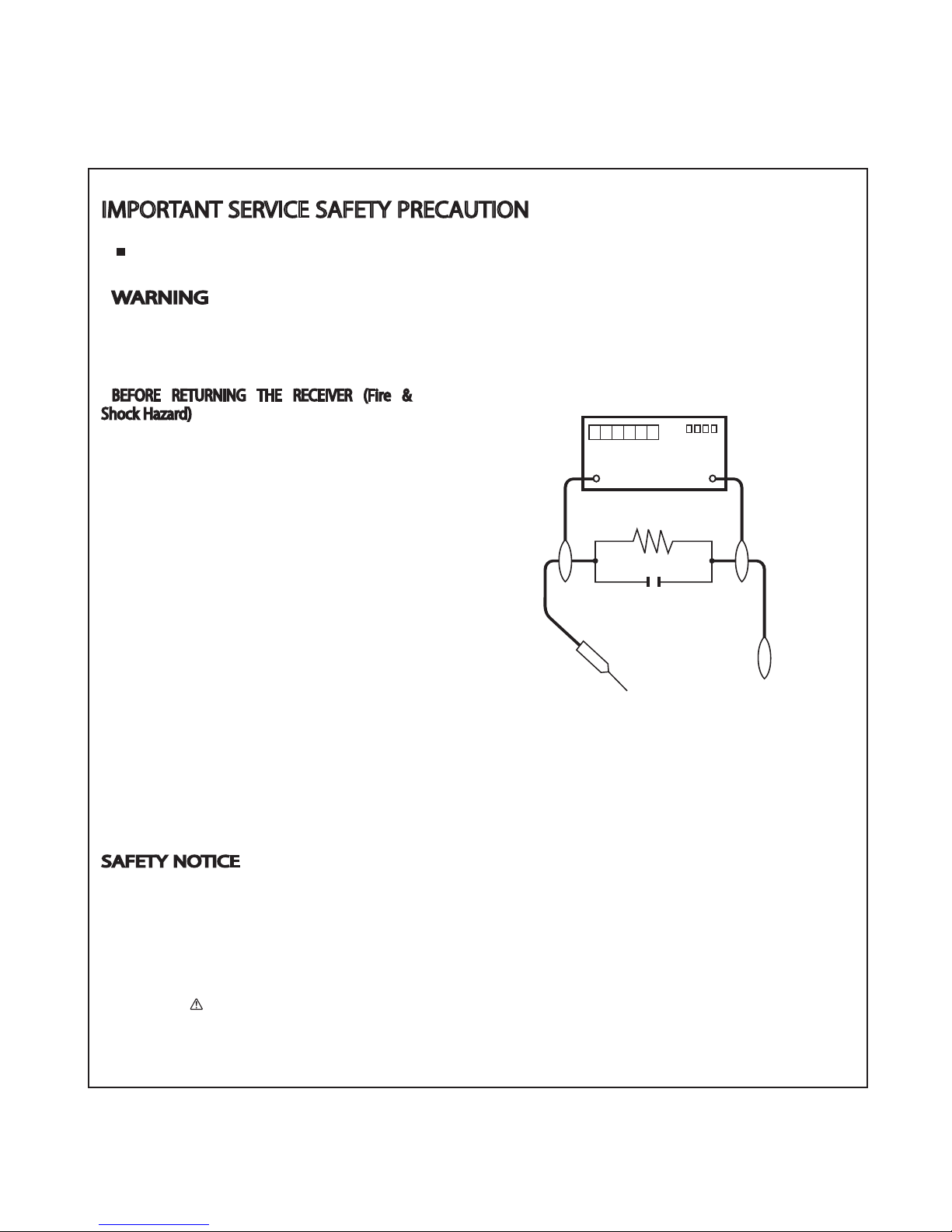
IMPORTANT SERVICE SAFETY PRECAUTION
WARNING
1. For continued safety, no modification of any circuit should be
attempted.
2. Disconnect AC power before servicing.
BEFORE RETURNING THE RECEIVER (Fire &
Shock Hazard)
Before returning the receiver to the user, perform the following
safety checks:
3. Inspect all lead dress to make certain that leads are not pinched,
and check that hardware is not lodged between the chassis and
other metal parts in the receiver.
4. Inspect all protective devices such as non-metallic control knobs,
insulation materials, cabinet backs, adjustment and compartment
covers or shields, isolation resistor-capacitor networks, mechanical
insulators, etc.
5. To be sure that no shock hazard exists, check for leakage current in
the following manner.
• Plug the AC cord directly into a 110-240 volt AC outlet.
• Using two clip leads, connect a 1.5k ohm, 10 watt resistor paralleled by a 0.15 F capacitor in series with all exposed metal cabinet
parts and a known earth ground, such as electrical conduit or electrical ground connected to an earth ground.
• Use an AC voltmeter having
with 5000 ohm per volt, or higher, sen-
sitivity or measure the AC voltage drop across the resistor.
• Connect the resistor connection to all exposed metal parts having a
return to the chassis (antenna, metal cabinet, screw heads, knobs
and control shafts, escutcheon, etc.) and measure the AC voltage
drop across the resistor.
All checks must be repeated with the AC cord plug connection
reversed. (If necessary, a nonpolarized adaptor plug must be used
only for the purpose of completing these checks.)
Any reading of 0.74 Vrms (this corresponds to 0.5 mA rms AC.) or
more is excessive and indicates a potential shock hazard which
must be corrected before returning the monitor to the owner.
///////////////////////////////////////////////////////////////////////////////////////////////////////////////////////////////
SAFETY NOTICE
Many electrical and mechanical parts in LCD colour television have
special safety-related characteristics.
These characteristics are often not evident from visual inspection, nor
can protection afforded by them be necessarily increased by using
replacement components rated for higher voltage, wattage, etc.
Replacement parts which have these special safety characteristics are
identified in this manual; electrical components having such features
are identified by " " and shaded areas in the Replacement Parts List
and Schematic Diagrams.
For continued protection, replacement parts must be identical to those
used in the original circuit.
The use of a substitute replacement parts which do not have the same
safety characteristics as the factory recommended replacement parts
shown in this service manual, may create shock, fire or other hazards.
///////////////////////////////////////////////////////////////////////////////////////////////////////////////////////////////
Service work should be performed only by qualified service technicians who are thoroughly familiar with all safety checks and the
servicing guidelines which follow:
DVM
AC SCALE
1.5k ohm
10W
TO EXPOSED
METAL PARTS
CONNECT TO
KNOWN EARTH
GROUND
0.15µF
TEST PROBE
Page 3
LC-60H20T/LC-70H20T
ii
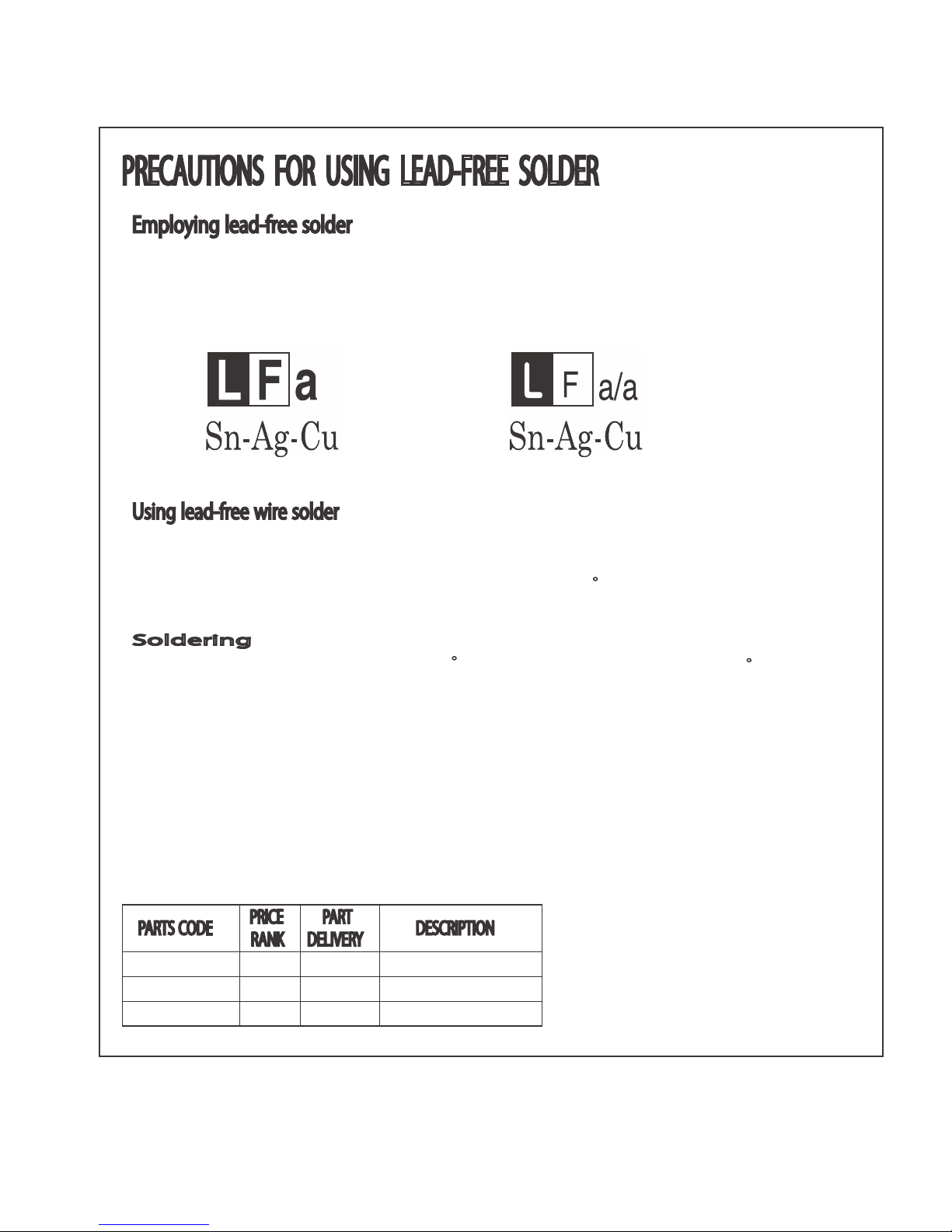
PRECAUTIONS FOR USING LEAD-FREE SOLDER
PRECAUTIONS FOR USING LEAD-FREE SOLDER
Employing lead-free solder
• “PWBs” of this model employs lead-free solder. The LF symbol indicates lead-free solder, and is attached on the PWBs and service manuals. The
alphabetical character following LF shows the type oflead-free solder.
Example:
Using lead-free wire solder
• When fixing the PWB soldered with the lead-free solder, apply lead-free wire solder. Repairing with conventional lead wire solder may cause damage or accident due to cracks.
As the melting point oflead-free solder (Sn-Ag-Cu) is higher than the lead wire solder by 40 C, we recommend you to use a dedicated soldering
bit, if you are not familiar with how to obtain lead-free wire solder or soldering bit, contact our service station or service branch in your area.
Soldering
• As the melting point oflead-free solder (Sn-Ag-Cu) is about 220 C which is higher than the conventional lead solder by 40 C, and as it has poor
solder wettability, you may be apt to keep the soldering bit in contact with the PWB for extended period of time. However, Since the land may be
peeled off or the maximum heat-resistance temperature of parts may be exceeded, remove the bit from the PWB as soon as you confirm the
steady soldering condition.
Lead-free solder contains more tin, and the end of the soldering bit may be easily corroded. Make sure to turn on and off the power of the bit as
required.
If a different type of solder stays on the tip of the soldering bit, it is alloyed with lead-free solder. Clean the bit after every use ofit.
When the tip of the soldering bit is blackened during use, file it with steel wool or fine sandpaper.
• Be careful when replacing parts with polarity indication on the PWB silk.
Lead-free wire solder for servicing
Indicates lead-free solder of tin, silver and copper. Indicates lead-free solder of tin, silver and copper.
PARTS CODE
PRICE
RANK
PART
DELIVERY
DESCRIPTION
ZHNDAi123250E BL J 0.3mm 250g (1roll)
ZHNDAi126500E BK J 0.6mm 500g (1roll)
ZHNDAi12801KE BM J 1.0mm 1kg (1roll)
Page 4
LC-60H20T/LC-70H20T
iii
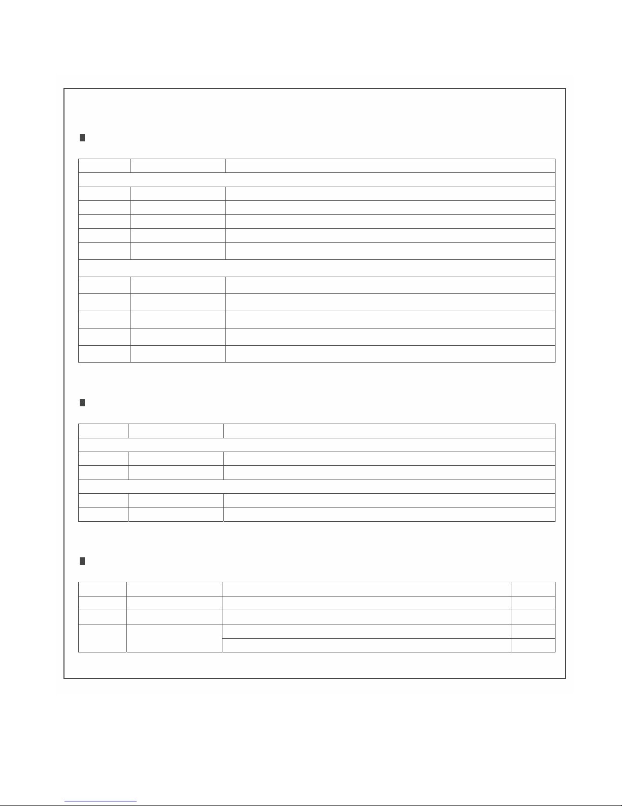
OUTLINE-MAJOR SERVICE PARTS
PWBUNIT
cseD.oNtraP.oNfeR
ripti
on
LC-60H20T
N
DKEYMG542FM01
MAINUnit
N DUNTKG505FM01 COCOROEYE
NDUNTKG504FM01
NETBOARD
N RUNTKB285WJQZ POWER Unit
N DUNTKG477FMG1
T-CON
Unit
LC-70H20T
N
DKEYMG542FM02
MAINUnit
N DUNTKG505FM01 COCOROEYE
NDUNTKG504FM01
NETBOARD
N RUNTKB286WJQZ POWERUnit
N DUNTKG477FMG2
T-CON
Unit
OTHERUNIT
cseD.oNtraP.oNfeR
ripti
on
LC-60H20T
N R1JE601D3HA10W
60"TFTLCD OpenCell
N CLCDTA375WEA4
60”PanelAssemblyUnit
LC-70H20T
N R1JE695D3HC50W
70"LCDPanel Module
Unit
N CLCDTA376WEA4
70”PanelAssemblyUnit
SERVICE
JIGS
cseD.oNtraP.oNfeR
ripti
Qno
ʼty
N QCNW-C222WJQZ ConnectingCor 2lenaPDCL-noC-T,d
1)WL(noC-T-niaM,droCgnitcennoCZQJW676F-WNCQN
NQCNW-N846WJPZ
Connectin
g
Cord, Main-T-Con (PL ) 1
ConnectingCord, Main-Power ( PD ) 1
Page 5
LC-60H20T/LC-70H20T
1 – 1
CHAPTER 1. SPECIFICATIONS
[1] SPECIFICATIONS
Specifi cations
T02H07-CLT02H06-CLledoM metI
mc 771mc 251lenap DCL
Resolution
2,073,600 pixels (1920 g 1080)
06 LAP/34.4 CSTN/85.3 CSTN/MACES/LAPmetsys ruoloc oediV
TV function TV-standard Analogue NTSC: M
Digital DVB-T
Receiving
channel
VHF/UHF 44.25—863.25 MHz
Digital VHF 470—806 MHz
TV-tuning system Auto Preset 135 ch
STEREO/BILINGUAL BTSC system
º671 :V º671 :Hselgna gniweiV
Audio amplifi er/Speakers
10 W g 2 / 4.5 g 10 cm 2pcs
Terminals
Antenna input
UHF/VHF/CATV 75 q F type
輸入1
(INPUT 1) (HDMI/ARC) HDMI (HDMI input)
輸入2
(INPUT 2) (HDMI/MHL) HDMI (HDMI input)
輸入3
(INPUT 3)/
輸入4
(INPUT 4)/
輸入5
(INPUT 5) (HDMI)
HDMI (HDMI input)
輸入6
(INPUT 6) VIDEO in, AUDIO in, COMPONENT in
輸入7
(INPUT 7)
VIDEO in, AUDIO in
電腦
bus-D inim nip 51)CP(
聲音輸出
(AUDIO OUT) AUDIO out
聲音輸入(
HDMI 5 /
電腦)
AUDIO IN (HDMI 5/PC)
3.5 mm jack*
1
BSU2 BSU/1 BSU
輸出
(OUTPUT) USB
rotcennoc elam bus-D nip 9C232-SR
數位聲音輸出
(DIGITAL AUDIO
OUTPUT)
Optical Digital Audio Output
Headphone
3.5 mm stereo
乙太網路
(ETHERNET)
(10/100 BASE-T)
Network connector
esenihC lanoitidarT/hsilgnEegaugnal DSO
zH 06 ,V 011 CAtnemeriuqer rewoP
)ybdnatS W 5.0( W 902)ybdnatS W 5.0( W 571noitpmusnoc rewoP
Dimensions without stand
1,355 (W) g 817 (H) g 86 (D) mm 1,563 (W) g 934 (H) g 87 (D) mm
with stand
1,355 (W) g 835 (H) g 350 (D) mm 1,563 (W) g 952 (H) g 350 (D) mm
)gk 73( gk 43)gk 72( gk 42)dnats htiw( dnats tuohtiw thgieW
C°04 — C°0erutarepmet gnitarepO
*
1
The HDMI 5 and
電腦
(PC) terminals can both use the same audio input terminal.
• As a part of policy of continuous improvement, SHARP reserves the right to make design and specifi cation changes for
product improvement without prior notice. The performance specifi cation fi gures indicated are nominal values of production
units. There may be some deviations from these values in individual units.
CAUTION
• Installing the Liquid Crystal Television requires special skill that should only be performed by qualifi ed service personnel.
Customers should not attempt to do the work themselves. SHARP bears no responsibility for improper mounting or mounting
that results in accident or injury.
• Carefully read the instructions that come with the bracket before beginning work.
Page 6

LC-60H20T/LC-70H20T
2 – 1
CHAPTER 2. OPERATION MANUAL
[1] OPERATION MANUAL
Attaching the stand
• Before attaching (or detaching) the stand, unplug the AC cord from the AC outlet.
• Before performing work spread cushioning over the base area to lay the TV on. This will prevent it from being damaged.
1
Confi rm the screws supplied with the TV.
(Six long screws and four short screws)
2
Insert the support angle into the stand base slot holes. (
1
)
• Please make sure left support angle into the left stand base and right support angle into the right stand base
(left side part engraved “L”, right side part engraved “R”).
3
Push the support angle follow the direction of the arrow mark on the stand base.
Push
Push the support angle follow
the direction of the arrow mark
4
For easily, user can use polystyrene foam as a jig to hold the stand base when fi xing by using the long
screws. (
2
)
2
Example for left side
2
5
Insert the stand into the openings on the bottom of the TV. (
3
)
6
Insert and tighten four short screws into the holes on the rear of the TV. (
4
)
Soft cushion
OUTPU
T
DC
5
V
1
.5A
H
D
MI
4
HDMI
5
U
SB
2
DC5V 0
.5A
AU
DI
O IN
D
IGI
T
AL
AUDIO
OUTPU
T
ANALOGU
E
RGB
(
PC
)
ARC
PC
H
DMI
1
INPUT 6
INPUT 7
AUDIO OUT
R
-
AU
DIO -
L
R -
AUDIO -
L
R
-
AUD
I
O
L
V
I
D
E
O/
Y
P
B
(C
B
)
P
R
(C
R
)
C
OMPO
NEN
T/
A
V
INPU
T
VIDEO
RS-232C IOIOI
US
B
1
D
C
5V
1
.
5A
(D
C5V
90
0
m
A
)
A
UD
I
O
(
L
/
R)
C
.I
.
M
H
L
HDMI 2
HDM
I 3
OUTPUT
3
4
NOTE
• To detach the stand, perform the steps in reverse order.
• Refer “Building the Work Table” in carton box to assemble the TV.
CAUTION
• Do not attach or detach the stand without holding it.
Doing so can cause the stand to fall, resulting in serious personal injuries as well as damage to the stand.
• The illustrations used throughout this manual are based on LC-60LE660X.
Polystyrene foam
Page 7
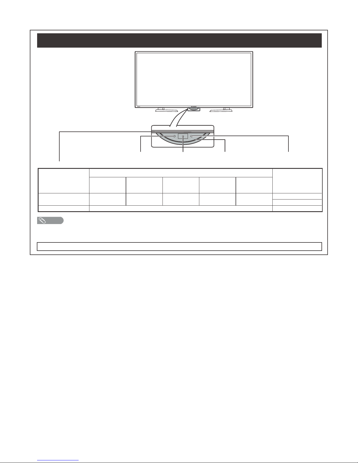
LC-60H20T/LC-70H20T
2 – 2
TV (Front)
RGB sensorRemote control sensor Motion sensor Power indicator
COCORO EYE LED
COCORO EYE LED
Power On mode (Power indicator lighted)
Standby mode
(Lighted)
Smart Power
Control
Auto Colour
Adjustment
Assist Light
mode
Optical
Picture
Control
Normal
ON
Green*
1
White White White Blue
Red
White (ASL is On)*
2
OFF
deRDEL oN
NOTE
*1 “SMART POWER CONTROL” IS PRIORITY. Power indicator will display Green even if other setting also turn On at the same
time.
*
2
If the “Assist Light mode” is turned On, Power indicator will display weak White during standby mode.
• The illustrations used throughout this manual are based on LC-60H20T.
Page 8
LC-60H20T/LC-70H20T
2 – 3
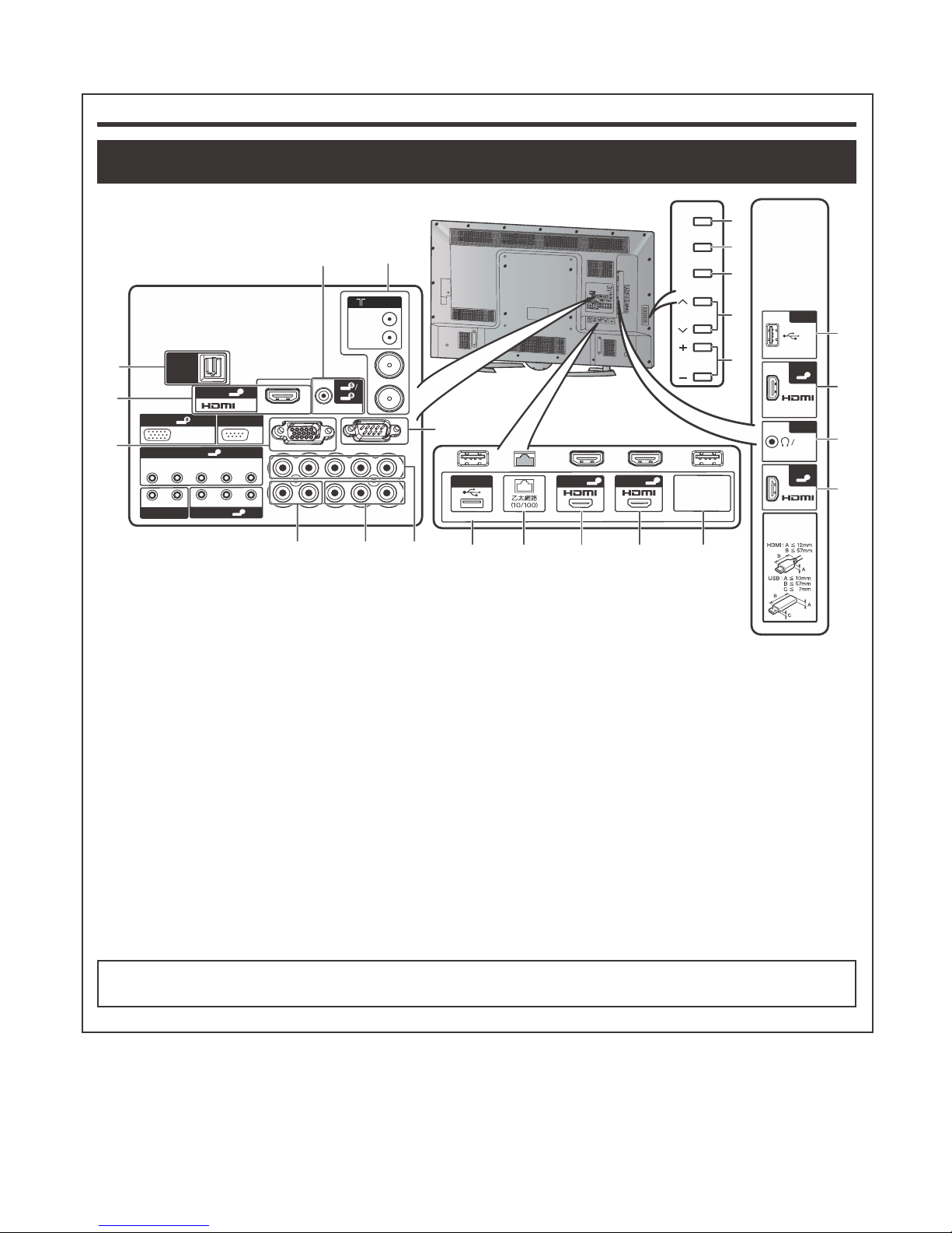
TV (Rear)
ARC
1
3
䴱㞜
2
䕮࠰
DC5V 1.5A
4
5
USB 2
DC5V 0.5A
䕮࠰
DC5V
1.5A
HDMI 5
6
䕮ޛ 6
7
䕮ޛ 7
㚨丩䕮࠰
-
㚨丩
-
ᐜ
-
㚨丩
-
ᐜ
-
㚨丩
-
ᐜ
ᖧ܅Y
P
B
(C
B
)
P
R
(C
R
)
㢨ᐤᖧ܅䕮ޛ
ᖧ܅
ᮮփ㚨丩
䕮࠰
㚨丩䕮ޛ
⌞ᝅ
ᴶ֩Ⲻ䙙ᯯᕅᱥֵ
⭞ޭᴿHDMI/USB
ㄥᆆ䁣ۏҁ⭘Ⱦ
(DC5V 900mA)
㚨丩ᐜ
RS-232C IOIOI
䕮ޛ 1
五∊
RGB
䴱㞜
HDMI 4
HDMI 3
HDMI 2
USB 1
MHL
䴱
Ⓠ
ⴤ
䤺
䕮
ޛ
乱
䚉
丩
䠅
❗㐐䴱㿌
ᴿ㐐䴱㿌
ཟ㐐ㄥᆆ
8
9
7
6
1
2
3
4
5
14 1213 11 10
15
16
17
23
21 2220
1918
1
電源
(POWER) (On/Off) button
2
目錄
(MENU) button
3
輸入
(INPUT) button
4
頻道
r/s
(CH r/s) buttons
5
音量
e/f (VOL e/f) buttons
6 USB 1 terminal
7 HDMI 2 (INPUT 2) (HDMI/MHL) terminal
8
輸出
(Headphones/
聲音(左/右)
) terminal
• The speakers do not output volume when
headphones are plugged in.
9 HDMI 3 (INPUT 3) (HDMI) terminal
10
輸出
(OUTPUT) terminal (For power output only)*
1
11 HDMI 4 (INPUT 4) (HDMI) terminal
12 HDMI 5 (INPUT 5) (HDMI) terminal*
2
13
乙太網路
(ETHERNET) (10/100) terminal
14 USB 2 terminal
15
數位聲音輸出
(DIGITAL AUDIO OUTPUT) terminal
16
輸入1
(INPUT 1) (HDMI/ARC) terminal
17
電腦
(PC) terminal*
2
18
聲音輸入
(AUDIO IN) terminal
19 Antenna terminals
(無線電視 / 有線電視)
20
聲音輸出
(AUDIO OUT) terminals
21
輸入7
(INPUT 7)
(影像 / 聲音(左 / 右))
terminals
22
輸入6
(INPUT 6)
(色差端子 / 聲音(左 / 右))
terminals
23 RS-232C terminal
*
1
This terminal can supply power for dongles. (Availability is depend on the specifi cation of dongle).
*
2
The HDMI 5 and
電腦
(PC) terminals can both use the same analogue audio input terminal. However, the proper item must
be selected in the “Audio select” menu.
• The illustrations in this operation manual are for explanation purposes and may vary slightly from the actual operations.
• The illustrations used throughout this manual are based on LC-60H20T.
Part names and functions
Page 9
LC-60H20T/LC-70H20T
2 – 4
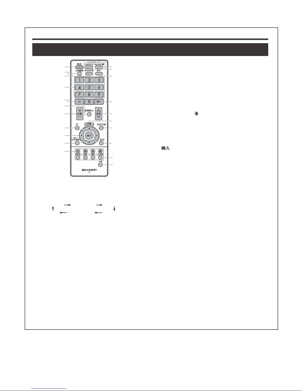
Part names and functions
Remote control unit
1
2
5
7
8
9
11
6
3
4
12
13
14
15
16
17
18
10
19
20
21
9 a/b/c/d (Cursor)
Select a desired item on the setting screen.
確定
(ENTER)
Execute a command.
10
色彩調整 (靜止
) [(COLOUR ADJ.) (FREEZE)]
Freeze a motion picture on the screen and adjust the
colour tone of the still image.
11 紅/綠/黃/藍 (R/G/Y/B) (Colour) buttons
The coloured buttons are correspondingly used to select
the coloured items on the screen.
12
輔助燈
(ASSIST)
To turn on/off Assist Light mode.
13
自動調色
(AUTO COLOUR)
To turn on/off Auto Colour.
14
照片
(PHOTO)
Display your pictures directly on the TV screen.
15
(INPUT) (INPUT SOURCE)
Select an input source.
16
頻道
r/s (CHr/s)
TV input mode: Select the channel.
(
頻道
r
) Increase the channel number.
(
頻道
s
) Decrease the channel number.
17
目錄
(MENU)
Display the menu screen.
18
音頻切換
(MPX)
Select the sound multiplex mode.
19
返回
(RETURN)
MENU mode: Return to the previous menu screen.
20
節目表
(EPG)
DTV mode: To display EPG (Electronic Programme Guide)
screen.
指南
(GUIDE)
DTV mode: Display the programme channel list.
資訊
(INFO)
DTV mode: Display the programme information.
收音機
(RADIO)
Press to access RADIO mode.
21
字幕
(SUBTITLE)
Switch subtitle languages on/off.
1
電源
(POWER) (STANDBY/ON)
To switch the power on and off.
2
定時關機
(SLEEP)
Set the Sleep timer.
0 hr. 30 min. 1 hr. 00 min.
2 hr. 30 min.
1 hr. 30 min.
2 hr. 00 min.
Off
3
網路娛樂
(INTERNET)
Press to select internet link.
4 0 – 9
Set the channel.
5 A (Flashback)
Press A to return to the previous selected channel or
external input mode.
6
螢幕顯示
(DISPLAY)
Display the channel or input information.
7
音量
k/l (VOLk/l)
Set the volume.
(
音量
k
) Increase the volume.
(
音量
l
) Decrease the volume.
8 e (Mute)
Press e s Mutes sound.
Press e again s Restores sound.
Mute will be cancelled after 30 minutes. However, the TV
will not suddenly output loud sound as the volume level
will be set to 0 automatically. Increase the volume level by
pressing
音量
k
(VOLk).
Page 10
LC-60H20T/LC-70H20T
3 – 1
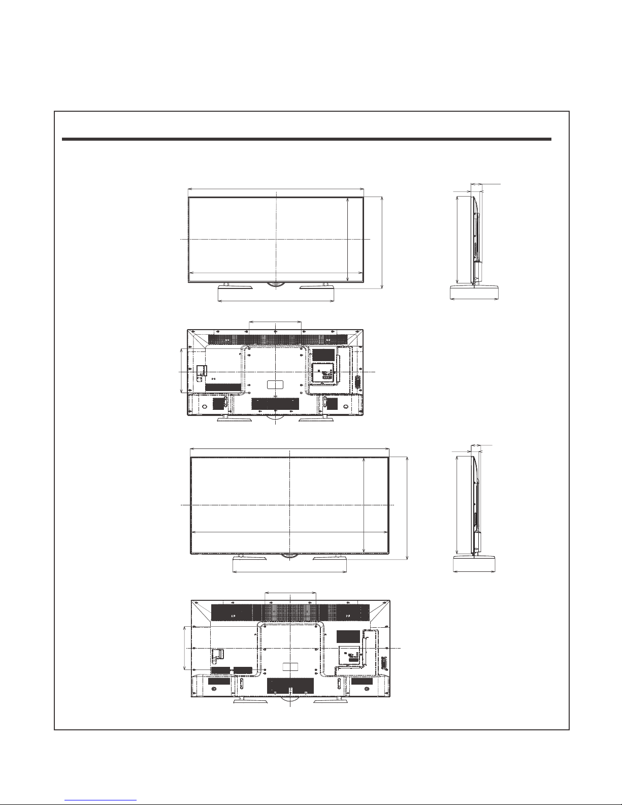
CHAPTER 3. DIMENSIONS
[1] DIMENSIONS
Dimensional drawings
400
400
400
400
86
69
350
817
1355
1332.4
901
835
754.3
1540.6
1563
901
952
871.5
LC-60H20T
LC-70H20T
87
69
350
934
Unit : mm
Page 11
LC-60H20T/LC-70H20T
4 – 1
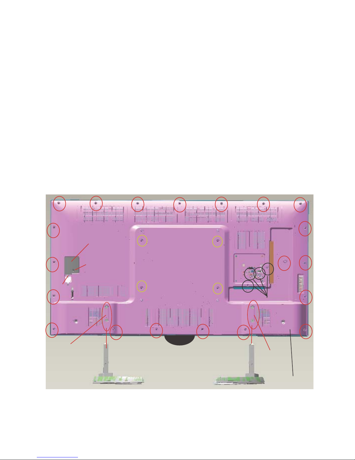
CHAPTER 4. REMOVING MAJOR
PARTS
[1] REMOVING MAJOR PARTS
[1] REMOVING OF MAJOR PARTS
REMOVING OF THE STAND UNIT AND REAR CABINET
1.Remove the 4 lock screw [1] and detech stand unit [2].
2.Remove 1 lock screw [3] and detech the AC cord cover [4].
3.Disconnect AC Cord [5].
4.Remove the 20 lock screws [6],remove 4 screw [7],remove 4 screw [8]. (LC-60LE360X)
Remove the 28 lock screws [6],remove 4 screw [7]. (LC-70LE360X) refer next page.
5.Detech rear cabinet assmbly [9].
[1]
[1]
[2]
[2]
[3]
[4]
[5]
[6]
[6]
[6]
[6]
[6]
[6]
[6]
[6]
[6]
[6]
[6]
[6]
[6]
[6]
[6]
[6]
[6]
[6]
[6]
[7]
[7]
[7]
[7]
[6]
[8]
[9]
LC-60LE360X
Page 12
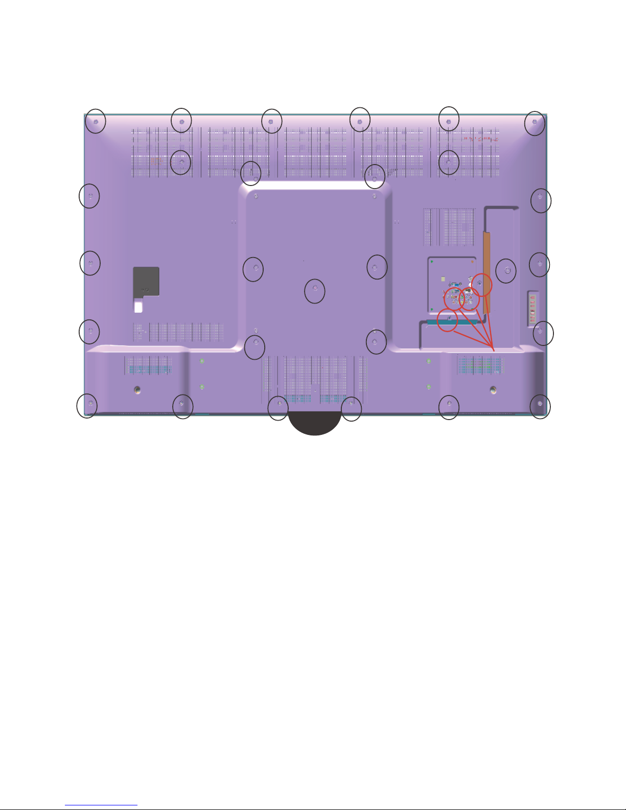
LC-60H20T/LC-70H20T
4 – 2
LC-70LE660X
[6]
[6]
[6]
[6]
[6]
[6]
[6]
[6]
[6]
[6]
[6]
[6]
[6]
[6]
[6]
[6]
[6]
[6]
[6]
[6]
[6]
[6]
[6]
[6]
[6]
[6]
[6]
[6]
[7]
Page 13
LC-60H20T/LC-70H20T
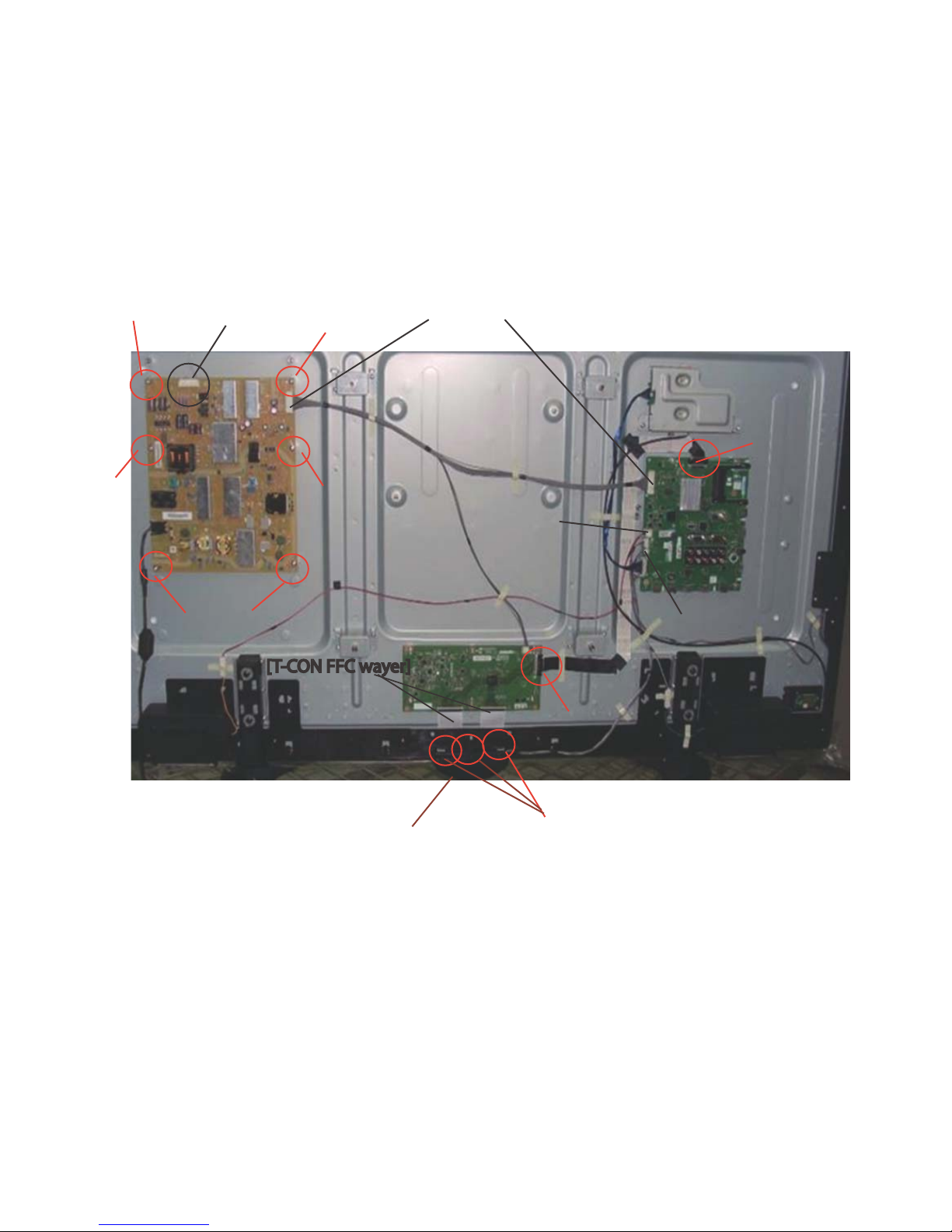
4 – 3
[2] Removing of connectors & PWB
1.Disconnect the following connectors from Main Unit. (SP,RA,KM,LWwires)
2.Disconnect the following connectors from the POWER Unit.(PD,PL,LED wire)
3.Disconnect the following connectors from the LCD CONTROL Unit .(T-Con FFC wayer)
4.Remove 4screws [1]Main Unit ,remove 6 screws [2] Power unit & remove 4 screws [3]
T-CON board,remove 3 screws [4] cocoro eye
[2]
[2]
[2]
[2]
[2]
[2]
LED Wire
[PD]
[PL]
COCORO EYE
[4]
[RB]
[KM]
[T-CON FFC wayer]
[LW]
[LW]
Page 14
LC-60H20T/LC-70H20T
5 – 1
CHAPTER 5. ADJUSTMENT
[1] ADJUSTMENT
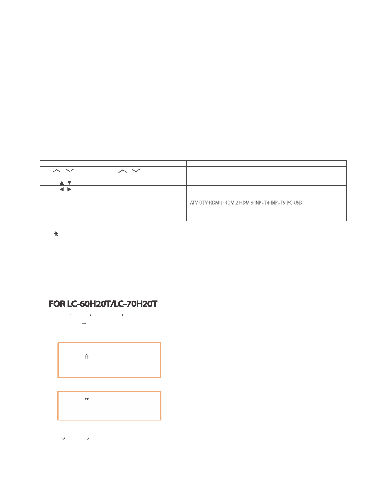
1.Enteringandcanceltheadjustmentprocessmode
1) WhileholdingdowntheINPUT andVolumeDOWNkeysatthesametime,plugintheACcordtoturnonthepower.(“K”standingfo rinspectionprocessmodeisdisplayedontheupperleftpositionofthescreen.)
2) PresstheChannelDOWNandVolumeDOWNkeysatthesametime.(Theadjustmentprocessmodescreenappears.)
3) Tocancelit,turnoffthepowerusingthePowerswitchorremotecontrol.
2.Remotecontrollerkey operationanddescriptionofdisplayinadjustment processmode.
1. keyoperation
* Inputmodeisswitchedautomaticallywhenrelevantadjustmentisstartedsofarasthenecessaryinputsignalisavailable.
noitcnuFyektinuniaMyekrellortnocetomeR
CH( / )
CH( / )
Changingchannel(UP/DOWN)
)NWOD/PU(emulovgnignahC)‒/+(LOV)‒/+(LOV
Cursor( / )
)TXEN/SUOIVERP(egapagninruT
Cursor( / )
)01-/01+(gnittesenildetcelesagnignah
C
INPUTbuttononremotecontroller
)gnihctiwselggot(gnihctiwsecruostupnInottubTUPNI
ENTER
3.So wareupgrading
1)MakesureLCDTVison.
2)InsertUSBdevicetotheUSBterminalattheLCDTV.
(MakesurethelatestsoftwareisinstalledintheUSBdevice.)
3)Usebelowmenuproceduretostartupgradingsoftwareversion:
4)Afewsecondlater,thesoftwareupgradingwillstartautomatically.
So wareUpdate(USB)
1%
ATV-DTV-HDMI1-HDMI2-HDMI3-INPUT4-INPUT5-PC-USB
-Menu
Option
Systemdata
-Areyousure?
Yes
II
I
USBdatatrans
5)Softwareissuccessfullyinstalledwhenthefollowingappearsattheendoftheprocess.
6)Onceupdatingcompleted,LCDTVwillbeautomaticallyoffandagain,afterfewseconds,automaticallyrestart.
7)Menu
S
etup
Identification
So wareUpdate(USB)
100%
FOR LC-60H20T/LC-70H20T
Page 15
LC-60H20T/LC-70H20T
5 – 2
LCD TV ADJUSTMENT ITEM
1. VCOM ADJUSTMENT
i. Enter service mode key and go to VCOM/TEST PATTERN Page
ii. Press “Enter” key (at VCOM)
iii. Adjust the flicker effect by pressing “VOL +/-“ of RC key
iv. Press “Enter” key after get the best value
2. SOFTWARE PACKAGE
i) Main Software
egakcaP erawtfoS ledoM
LC-60H20T
LC-70H20T
Wisteria_Taiwan_Pack15_vXXX.bin
Main Software Filename : XXX is Software version
Please manually change the panel inch setting (60” or 70”) according to the model.
If any changes of software, will be informed by MARUHEN.
ii) Net Software
krameR egakcaP erawtfoS ledoM
LC-60H20T
LC-70H20T
wisteria660_netboot_vXXXX.bin For Bootloader ( write at ISP Flash)
wisteria660_net_vXXXX.bin Net Software ( write at NAND Flash)
Net Software Filename : XXXX is Software version
iii) Sub Software
egakcaP erawtfoS ledoM
LC-60H20T
LC-70H20T
Wisteria660_Sub_VXXX.production.hex
Sub Software Filename : XXX is Software version
Page 16
LC-60H20T/LC-70H20T
5 – 3
3. T-CON ROM DATA INPUT (T-CON PWB : QPWBXG477WJ**)
ERUDECORP NOITIDNOC METI
1 T-CON Data
Input
(T-CON PWB)
Checker
adjustment
Full version
confirmation
1. At checker, connect software jig at CN5801 (TL5801~5807).
2. Input voltage at P4804 (TL4839~TL4880) and ROM start to
input data.
3. Power OFF after finish data input.
[ Caution item ]
If some error happened, ROM data is not written in at all.
Note: Please refer to below for combination of T-Con software
LCD PANEL T-CON UNIT T-CON SOFTWARE
1
R1JE601D3HA10W
(LC-60H20T)
DUNTKG477FMG1
SHARP_71912_FW_(v20140924_60425110)_SPI.bin
2
R1JE695D3HC50W
(LC-70H20T)
DUNTKG477FMG2
SHARP_71912_FW_(v20140924_70425100)_SPI.bin
4. MAC ADDRESS & WMDRM PROGRAMMING
(Key is from Sharp IT department)
One key is for every each unit except the WMDRM key. Please be extra careful in data management so
as NOT to write multiple data. Also, when data writing location parts is broken, please change PWB board
(since the concerned IC is non-exchangeable part).
Note: a) MAC Address is from Sharp IT department
b) WMDRM Key is from SEM Enginering department
5. SIGNAL ADJUSTMENT
A. PICTURE ADJUSTMENT
Confirmation of signal from generator (setting to spec le
vel)
PAL Composite signal 㸸0.7Vp-p s 0.02Vp-p (pedestal to white level)
15K Component signal (50Hz) 㸸Y level 㸸0.7Vp-p s 0.02Vp-p (pedestal to white level)
Pb, Pr level 㸸0.7Vp-p 㸸0.7Vp-p s 0.02Vp-p
33K Component signal 㸸Y level 㸸0.7Vp-p s 0.02Vp-p (pedestal to white level)
Pb, Pr level 㸸0.7Vp-p 㸸0.7Vp-p s 0.02Vp-Com
Page 17
LC-60H20T/LC-70H20T
5 – 4
a) Adjustment Mode
NO. ERUDECORP NOITIDNOC METI
1 Adjustment Mode Press the test key at the test remote control
b) Component 15K 50Hz Signal Adjustment (COMP-SD)
NO. ERUDECORP NOITIDNOC METI
1 Setting [Signal]
COMP 15K 50Hz
(576i)
100% Full-field
Colour Bar
[Terminal]
COMPONENT
INPUT 6
࣭Feed the COMPONENT 15K 50Hz (576i) 100% Full-field
Colour Bar signal(100% colour saturation) to
COMPONENT INPUT 3
2 Auto Adjustment Test Mode page 4
(COMP SD)
At the related page, move cursor to [COMP SD ADJ], press
ENTER.
[OK] appears when finished.
c) Component 33K 60Hz Signal Adjustment (COMP-HD)
NO. ERUDECORP NOITIDNOC METI
1 Setting [Signal]
COMP 33K 60Hz
(1080i)
100% Full-field
Colour Bar
[Terminal]
COMPONENT
INPUT 6
࣭Feed the COMPONENT 33K 60Hz (1080i) 100% Full-field
Colour Bar signal(100% colour saturation) to
COMPONENT INPUT 3
Page 18
LC-60H20T/LC-70H20T
5 – 5
2 Auto Adjustment Test Mode page 5
(COMP HD)
At the related page, move cursor to [COMP HD ADJ], press
ENTER.
[OK] appears when finished.
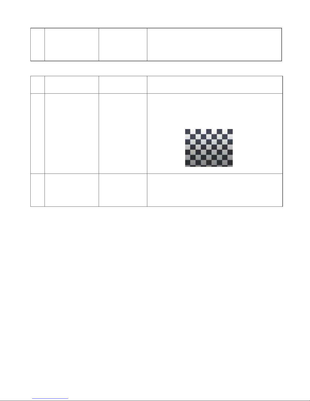
d) PC (ANALOG RGB) Signal Adjustment (PC-RGB)
NO. ERUDECORP NOITIDNOC METI
1 Setting [Signal]
XGA 60Hz
100% Checkered
Pattern
[Terminal]
PC INPUT 8
࣭Feed the XGA 60Hz 100% Checkered pattern signal (100%
colour saturation) to PC INPUT
䈜Please make sure SYNC is OFF.
2 Auto Adjustment Test Mode page 6
(PC-RGB)
At the related page, move cursor to [RGB ADJ], press
ENTER.
[OK] appears when finished.
Page 19
LC-60H20T/LC-70H20T
5 – 6
MGMB**** RB to the reference value of point 1.
(18) Adjusted value is writing at [command]
MSET0003
(19) Set the G of point Max. to the default value
(4080 x G value of point 2 / R2). Set the R,B
Max. value [G
max
– G value of point 2 + (R,B
value of point 2)
(20) Calculate the slope R2
slope,
G2
slope,
B2
slope
between MAX and Point2.
R2
slope =
(R
max
- R
high
)/(4080-3664)
(21) Calculate the correction value
پR
high, پGhigh, پBhigh.
پR
high = R2slope X
(3840-3664)
(22)
Set the reference value R,G,B of point 2
(R2䇻)=R2+پR
high
(23)
Calculate the slope R1
slope,
G1
slope,
B1
slope
between Point2 and Point1.
R1
slope =
(R
high
- R
low
)/(3664-480)
(24)
Calculate the correction value پR
low,
پG
low, پBlow.
پR
low = R1slope X
(538-480)
(25)
Set the reference value R,G,B of point 1
(R1䇻)=R1+پR
low
(26) Shut down the AC power.
䈜Initial value at RGB 2 point : 3664
䈜Initial value at RGB 1 point : 480
[Adjustment value]
ۼTeaching set send by engineering dept is set as
reference.
[Reference values for adjustment reference]
Equipment : Luminance meter [Minolta CA-210]
Level
Spec
Data
Adj. Spec.
Inspection
Spec.
Point
2 ref.
values
229
x=0.2685
y=0.267
0.0010 0.0020
Point
1 ref.
values
30
x=0.2685
y=0.267
0.0045 0.0090
Ref. : For inspection, set the LCD TV as below.
AV MODE : [DYNAMIC] (Reset)
Aging Time : Minimum 30 minutes
RESULT
+
-
+
-
+
-
+
-
Page 20

LC-60H20T/LC-70H20T
5 – 7
6. FACTORY SETTING
AC power is plug off after shipment setting is done.
Caution
: Do not plug on again after shipment setting is done. If do, please re-do the shipment setting. Do not off
with remote control.
Model Name Factory Setting
Key Name
Remote Control
Code
S-System Setting OSD Language
Setting
A3LCRH20T
A3LCTH20T
T-Setting 100000111111110 M
TRADITIONAL
CHINESE/
ENGLISH
ITEM ERUDECORP NOITIDNOC
Factory setting AC power off to exit
the factory setting.
1. Setting is done with test remote control.
2. Press the ‘Factory Setting’ key on the remote control continuously.
3. When Green background appears on screen and ‘K’ mark
disappears, setting is completed.
The followings are initialised to factory setting:
1) User setting
2) Channel data (e.g. broadcast frequencies)
3) Manufacturer’s option settings
4) Password data
5) Setting values are set based on model destination
Page 21

LC-60H20T/LC-70H20T
5 – 8
[2] USB CLONE SPECIFICATIONS
[3] USB CLONE SPECIFICATIONS
[2] USB Clone (Smart Loader)
1. Description
The Smart Loader is a function implemented in the service software to easily replicate the user settings of one TV into another.
These settings include (but not restricted to): picture and audio, turning set-up, language and country selection, PIN, child locked programs etc.
Factory adjustments are not copied as they are different for every TV.
The Smart Loader makes possible the user data to be stored in a memory device connected to the USB terminal of the TV that is used as reference
and later load those data into other TVs by using their respective USB terminal.
2. How it works
1. Enter USB clone menu (Smart Loader)
i) Press panel key [INPUT] and [VOL+] and AC on, it will go to password entry OSD
ii) Enter digit “369” then it will go to Smart Loader Menu
2. Smart Loader function
i) SMLD Store
• To copy all related data fro
m TV -> USB and put under a fixed filename “SHPSMLD.bin” (8kB).
ii) SMLD Restore
• To restore the related data from USB -> TV.
iii) SMLD Store and Restore execution
• To execute SMLD Store or SMLD Restore, highlight at selected item and press Enter.
• After cloning process is done, “OK” is displayed.
If cloning process is not finished due to error (e.g. no pendrive detected), “NG” is displayed.
3. Exit USB Clone menu (Smart Loader)
i) To exit Smart Loader menu, plug off AC Cord.
SMLD Store SMLD Restore
2nd AQUOS TVUSB1st AQUOS TV
Page 22

LC-60H20T/LC-70H20T
5 – 9
[4] PUBLIC MODE SETTING
[5] PUBLIC MODE SETTING
[3] PUBLIC MODE SETTING PROCEDURE
1. How to start Public Mode
• There are the following two ways to get the public mode setup screen displayed.
1) Press the “INPUT” and “VOL (+)” keys on the set at once and turn on the power.
2) Get the password input screen displayed.
3) The 3-digit password is now verified.
The password [0] [2] [7] provides for the public mode screen. (This screen comes on with whatever adjustment process settings.)
With any other passwords, the screen changes to the normal mode.
In the adjustment process mode, turn on “PUBLIC MODE”. Also press the “CH ( )” and “VOL (+)” keys on the set at once and turn on the power.
2. How to exit Public Mode
There are the following ways to quit the public mode setup screen.
• Turn off “PUBLIC MODE” in the adjustment process mode. ( ) This way alone is not for quitting the setup screen, but for quitting the mode by
itself.
• Turn off the powe
r with the “POWER” key. ( )
• Select “EXECUTE”.( )
“PUBLIC MODE” stays on in the adjustment process mode.
The settings will be back to the factory ones.
3. Public Mode Setting Values
• With the factory settings made, the public mode settings get initialized. (The adjustment process remains intact.)
Procedure
• The input starts with the leftmost digit.
• Use the numeric keys [1] thru [9] and [10/0] keys on the remote controller.
The other keys are not acceptable.
• With a numeric-key input,“
“ will change to “ “. The input position will move one digit to the right.
• With all the 3 digits entered, the password will be verified.
Page 23

LC-60H20T/LC-70H20T
5 – 10
4. Public Mode Menu
The guidance is not displayed onscreen.
Setup procedure
• To move the cursor up and down, use the “cursor UP/DOWN” key (remote controller) and “CH ( )/( )” key (remote controller and set).
• To change the settings, use the “cursor RIGHT/LEFT” key (remote controller) and “VOL (+)/(‒)” key (remote controller and set).
• To save new settings, keep the cursor at “Execute” and use the “cursor RIGHT/LEFT” key (remote controller) and “VOL (+)/(‒)” key (remote controller and set).
5. On Setting Items
1. POWER ON FIXED
2. MAX V OLUME
Selection Variable/Fixed
Default Variable
Explanation When set to “Fixed”, the power cannot be turned off with the power key on the remote control or main unit, and the image
reception state is kept (it does not enter the standby state).
The power can be turned off by shutting off power supply from AC.
Limit in setting • Power key on the main unit/
remote control power supply key
• OFF timer/ON timer
Exception None
Remarks • Selection of “FIXED” assumes use of STB, etc.
• When set to “Variable”, if the main power switch is set to off, the power is turned off after a wait of 1 second.
(Push-push switch only)
• Display ON/OFF in the hotel menu is controlled by the adjustment process “HOTEL POWERFIX”.
• When the power button is operated, a caution is displayed (it times out in 5 seconds).
(For the caution, refer to the power on fixed message sheet.)
* The caution is not displayed when in the adjustment process, hotel menu, default setting, MCL operation and auto preset
(Ch search operation).
The OSD display including the menu and this caution have priority over all others.
When “OSD display” (described below) is set to “Variable”, this caution is displayed as a special case.
Selection Adjustment from 1 to 60 (no loop)
Def
ault 060
Explanation Sound volume can not be adjusted higher than the preset value.
Limit in setting • When the sound volume is set lower than 59, only figures are displayed and the sound volume bar is not displayed.
• The maximum sound volume for ON-timer (Wake up timer) is limited also to the preset value.
Exception • In the item “VOLUME” of adjustment process, the sound volume can be set freely irrespective of this setting.
Remarks • Setting is valid only for the speakers of the unit. (As for the headphone, the sound volume can be set up to 60 irrespective
of the limit.)
• In line output (sound volume variable), the sound volume can be adjusted from -60 to 0 irrespective of pre-adjusted value.
• When the sound volume is set higher than the MAX setting by the adjusting process or headphone, the sound volume con-
trol operation is prohibited for turn-up and the sound volume should be tu
rned down to MAX in this state.
<Example ofimage>
Page 24

LC-60H20T/LC-70H20T
5 – 11
3. VOLUME FIXED
4. VOLUME FIXED LEVEL
5. RC BUTTON
6. PANEL BUTTON
7. MENU BUTTON
Selection Selection between “Variable”,''Fixed'' and ''AC/RC CTRL'' ( loop provided ).
Default Variable
Explanation Sound volume is fixed and made invariable.
Limit in setting • The sound volume for the ON-timer (Wake up timer) is fixed also without display of menu. Besides, the setting is made
impossible. (Basically, the menu is not displayed.)
• The following keys become invalid:
1) Sound volume Up/Down (VOL +/-) [for both remote control and the unit]
2) Mute (MUTE)
Exception • In the item “VOLUME” of adjustment process, the sound volume can be set freely irrespective of this setting.
Remarks • In “Variable” setting, the sound volume had been conventionally set at 1 but this operation has been abolished (and follows
the last memory).
•
The sound volume for the ON
-time is not set at 1 either and the sound volume set value of the ON-timer before the hotel
mode is executed.
• Setting is valid only for the speakers of the unit. (As for the headphone, the sound volume can be set up to 60 irrespective
of the limit.)
• In line output (sound volume variable), the sound volume can be adjusted from -60 to 0 irrespective of pre-adjusted value.
• As for sound volume fixing and sound volume MAX level, the sound volume fixing has priority.
• Once the sound volume has been changed by adjustment process or headphone, it should be set back to the sound volume
preset by sound volume fixing level when the adjustment process ends or when the headphone is removed.
Selection Adjustment from 1 to 60 (no loop)
Default 020
Explanation The sound volume to be fixed by “Volume fixed” is determined.
Limit in setting None
Exception None
Rem
arks Setting is valid only when “Volume fixed” is selected for “fixed”.
This must be confirmed actually by changing also the sound volume in accordance with setting.
Selection Selection between “Resp ond”and "No respond"( loop provide ).
Default Respond
Explanation Acceptability of keys by remote control is limited or reception of keys can be prohibited.
Limit in setting
1)
In “No respond” setting, all the keys (including the power key) are not accepted.
Exception • Adjustment process, factory setting, inspection process and hotel only keys are valid irrespective of setting.
• All the keys can be used in adjustment process, inspection mode and hotel menu irrespective of setting.
Remarks
Selection Selection between “Respond” and “No respond” (loop provide)
Default Respond
Explanation All the operations by keys (except the power key) of the unit can be invalidated.
Limit in setting
Exception • Inspection mode and hotel menu mode can be started irrespective of setting.
• All the keys ca
n be used in adjustment process, inspection mode and hotel menu irrespective of setting.
Remarks
Selection Selection between “Respond” and “No respond” (loop provide)
Default Respond
Explanation In “No respond” setting, the menu operation by the menu key of the remote control and the menu key of the unit is invalidated.
Limit in setting • ON-timer (Wakeup Timer) is turned OFF.
• The following keys become invalid.
Wake-up timer and clock setting keys and all of the direct change keys to menu display
Exception • Inspection mode and hotel menu mode can be started irrespective of setting.
• All the keys can be used in adjustment process, inspection mode and hotel menu irrespective of setting.
Remarks
•
In "AC/RC CTRL" the tv stars at the volume specified in the volume fixed level.The volume can be adjust by remote control
but after OFF.ON ,it will return to the volume fixed level.
Page 25

LC-60H20T/LC-70H20T
5 – 12
8. OSD DISPLAY
9. BLUE SCREEN
10.INPUT MODE START
11.INPUT MODE FIXED
Selection Selection between “Yes”, “No” (loop provide)
Default Yes
Explanation The following OSD displays are made ineffective.
Displays of menu group, channel call, sound volume bar and direct key call
Limit in setting • Set time of the OFF-timer (SLEEP TIMER) is cleared.
• Setting of the no-signal power-OFF (AUTO POWER OFF) is cleared to “OFF”.
• Setting of the no-operation power-OFF is cleared to “OFF”.
• Keys falling under any of the following items become invalid.
1) Appearance of screen changes and the sound changes.
2) Personal functions which are hard to restore.
Ex.) Screen display, menu, OFF-timer, ON-timer, AV MODE, screen size switching, clock setting, treble emphasis, AUDIO
ONLY, sound changeover, LANGUAGE, CLOSED CAPTION
Others • Simple input switching is generated. Those which are restored soon after leaving as they are and
may be requested for
change by customer are not prohibited.
Ex.) Brightness sensor (BACKLIGHT) and PIC. FLIP
Exception • Such a caution which is displayed independently is displayed asitis.
Non-responding signal caution, TELE TEXT caution and power-ON fixing caution
Selection Selection between “Yes”, “No”
Default No
Explanation When no signal inputs, selecting the background color.
Selected to “Yes”---Blue screen
Selected to “No”---No Blue screen
Selection Selection between “Normal”, “ATV (CH~)'HDMI 1,HDMI 2,HDMI 3,COMPONENT,AV,PC,MEDIA (loop provide)
Default Normal
Explanation In power-ON, the input source to be started or channel can be set.
(In standard mode, the operation follows the last memory.)
About options • All the input sources in the model are made selectable.
• When the input/output switchable input source is selected and the input source is set to output, the setting ofinput/output
switching is changed to input at the execution of hotel menu. In addition, the input/output switching
by menu is prohibited.
• In TV mode, the display of all channels is stopped and it is treated as an input source. At this time, the channel to be set follows the last memory and the content of the last memory is included in the notation by options. Ex.) TV (CH2), TV (CH4)
etc.
• The order of appearance of options in the hotel menu should agree with the order of toggles by input switching key.
Limit in setting • The display of channel setting menu and the channel setting operation are prohibited (except for MCL).
Exception None
Remarks • In setting at “Normal”, the setting of “Input mode fixed” is changed to “Variable” and selection should be prohibited.
Selection Selection between “Variable” and “Fixed” (loop provide)
Default ‒ (Variable)
Explanation The input mode is fixed at the input source or the channel set at the “Input mode start” in 10 and other input sources and chan-
nels can be made non-selectable
.
Limit in setting • With the execution of hotel mode, the input source is forced to change to that set by “Input mode start” and the channel
switching and input switching are prohibited thereafter.
• The following keys are invalidated.
CH , direct tuning button, FLASHBACK, input
*However, the keys (input switching and CH , keys) of the unit for menu operation remain valid.
Exception None
Remarks • In the following case, setting is cancelled and mode is changed to “Variable”.
When the setting of “Input mode start” is set to “Standard (Normal)”
Page 26

LC-60H20T/LC-70H20T
5 – 13
12.PRESET CHANNEL PLAN
Selection Selection between "ON" and "OFF"
Default OFF
Explanation [ON] : Display preset channel plan when power on.
[OFF]: Not display preset channel plan. (Default setting)
Remark When hotel mode is ON and PRESET CHANNEL PLAN is [ON],
press power ON (Panel or R/C key), it displays preset channel plan on the screen.
When
user press ENTER key during TV mode ,its shows preset channel plan.
Page 27

LC-60H20T/LC-70H20T
6 – 1
CHAPTER 6. TROUBLESHOOTING
TABLE
[1] TROUBLESHOOTING TABLE
[2] TROUBLESHOOTING TABLE
[1] TROUBLESHOOTING TABLE
No power (front LED failure to light up) or no startup (front LED failure to turn from red to blue)
Are the wire harnesses and other cables properly connected in
the set?
NO Reconnect the wire harnesses and other cables properly in the
set.
YES
Is there the PSONand PNLPOWsignal input at pins
(10 ) and (12
) of P9602?
NO Check the
PS-ON signal li ne PNL POWsignal line.
YES
Are the DC/DC converter outputs and the output voltages along
the control lines as specified?
NO Check the DC/DC converters and the control lines. Replace
defective parts as required.
1) M+5.6V (IC9601) 8) BU+3.3V (IC9604)
2) D+1.0V
(IC9612)
3) D+5V (IC9607)
4) BU+5V (D9610)
5) D+3.3V (IC9606)
6)
D+1.5V(IC9608)
7) D+1.15V
(IC9602)
9) D+2.5V (IC9605)
10) M+5.1V(IC9617)
Page 28

LC-60H20T/LC-70H20T
6 – 2
With [RF] signal input No video onscreen (1)
No video in the UHF/VHF reception
Is there IF output from the tuner pin(8),(9)of TU1102asspecified? NO Check TU1102 and its peripheral circuits.
YES
Is there IF input at pin W1 & W2 of IC3301 ? .1033CI&2011UTneewtebtiucricehtkcehCON
YES
NO Check IC3301 and its peripheral circuit to SC3801
YES
Check LVDS cable, LCD controller (incl. panel) and their peripheral circuits.
With <Video> signal input No video onscreen (2)
No external input video onscreen <INPUT 7>
Is INPUT 7 selected on the input select menu screen? NO Select INPUT 7 on the input select menu screen to pick up the
right input signal.
YES
Is there the video signal input at pin (R2) of IC3301? NO Check the line between pin (9) of J502 and pin (R2) of IC3301.
YES
NO Check IC3301 and its peripheral circuits to SC3801
YES
Check LVDS cable, LCD controller (incl. panel) and their peripheral circuits.
Are there the signal output
( P19-P20,R19-R21,T19-T21,V19-V21
W18-W21,Y18-Y21,AA18-AA20)ofIC3301toSC3801?
Are
there
the signal outputs pin ( P19-P20 , R19-R21 ,T19-
T21,U19-U20,V19-V21,W18-W21,Y18-Y21,AA18-AA20 ) of IC3301 to SC3801?
U19-U20
there
Page 29

LC-60H20T/LC-70H20T
6 – 3
With <Component> signal input No video onscreen (3)
No external input video onscreen <INPUT 6>
Is INPUT 6 selected on the input select menu screen? NO Select INPUT 6 on the input select menu screen to pick up the
right input signal.
YES
Are there the Y, Pb and Pr signal inputs at pins (L1), (L3) and
(M1
) of IC 3301 respectively?
NO Check the line between pins (15)/(17)/(19 )of J502 and pins (L1)/
(L3) /(M1) of IC3301.
YES
NO Check IC3301 and its peripheral circuitstoSC3801
YES
Check LVDS cable, LCD controller (incl. panel) and their peripheral circuits.
With <HDMI1/HDMI2 / HDMI3/HDMI4/HDMI5>signal input No video onscreen (4)
No external input video onscreen <INPUT 5/HDMI1/HDMI2/HDMI3/HDMI4>
ON
YES
YES
toSC3801?stiucriclarehpirepstidna1033CIkcehCONstuptuolangisehterehterA
YES
Check LVDS cable, LCD controller (incl. panel) and their peripheral circuits.
Are there the signal outputs
(P19-P20 ,R19-R21,T19-T21,U19-U20,
V19-V21,W18-W21,Y18-Y21,AA18-AA20 ) of IC3301toSC3801
Pin(P19-P20,R19-R21,T19-T21,U19-U20
,V19-V21,W18-W21,Y18-Y21 ,AA18-AA20 ) of IC3301 toSC3801
Select <HDMI1-HDMI5> on the input
select menu screen to pick up the right signal input
Check peripherel circuit between
IS HDMI1/HDMI2/HDMI3/HDMI4/HDMI5 selected on menu
screen ?
NO
Are there signal output from (SC1501/SC1503/SC1504/SC1506/SC1507)
(SC1501/SC1503/SC1504/SC1506/SC1507)
Page 30

LC-60H20T/LC-70H20T
6 – 4
No audio heard (1)
No sound in the UHF/VHF reception.
NO Check TU1102 and its peripheral circuits.
YES
Is there the 12C signal input at pins (W4 ), (W5) of IC3301? NO Check IC3301 and its peripheral circuits.
YES
stidna2071CIdna1033CIneewtebnoitcennockcehCON?2071CIfo)6(niptatuptnilangisoiduaerehtsI
peripheral circuits.
YES
Is the L-ch audio signal output at pin (26),(27)
NO Check IC1702 and its peripheral circuits.
of IC1702 normal?
YES
Are the audio signal L-ch and R-ch output at (3)/(4) and (1)/(2) of
P1701 normal?
NO Check circuit between IC1702 & P1701.
YES
Check speakers and their peripheral circuits.
(30),(31)
of IC1702 normal?
Is the R-ch audio signal output at pin (10
(11), (14) (15),
Is the IF output from the tuner pin(8) & (9)
of TU1102 as specified ?
Page 31

LC-60H20T/LC-70H20T
6 – 5
No audio heard (2)
No external audio heard
<INPUT 7>
Is there the L-ch audio signal input from pin (7) ofinput terminal
J502 to pin (U4) of IC3301?
Is there the R-ch audio signal input from pin (5) ofinput terminal
J502 to pin (V5
)ofI
C3301?
<INPUT 6>
Is there the L-ch audio signal input from pin (13) ofinput terminal
J502 to pin (T6) of IC3301?
Is there the R-ch audio signal input from pin (11) ofinput terminal
J502 to pin (T7) of IC3301?
YES
Is there the I2S signal output at pin ( J19),(J20) of IC3301 ? NO Check IC3301 and its peripheral circuits.
YES
ON?2071CIfo)6(niptatupnilangisoiduaerehtsI Check connection between IC3301 and IC1702 and its periph-
eral circuits.
YES
Is the L-ch audio signal output at pin(26), (27) ,(30),(31) of
IC1702 normal ?
NO Check IC1702 and its peripheral circuits.
Is the R-ch audio signal output at pin(10), (11),(14),(15) of
IC1702 norma
l?
YES
Are the audio signal L-ch and R-ch output at (3)/(4) and (1)/(2) of
P1701 normal?
NO Check circuit between IC1702 & P1701.
YES
Check speakers and their peripheral circuits.
Page 32

LC-60H20T/LC-70H20T
6 – 6
No audio heard (3)
ON?neercsnoraeppaegamiIMDHehtseoD
YES
.tonronettirwsiDIDEfitikcehCON<morftuptuooiduaoN
YES
Are waveforms input in to the pin(C4,D4/C3,D3/W7,V8)
of IC3301 normally?
NO Check peripheral circuits IC3301.
YES
ON?2071CIfo)6(niptatupnilangisoiduaerehtsI Check connection between IC3301 and IC1702 and its periph-
eral circuits.
YES
Is the L-ch audio signal output at pin(26), (27) ,(30), (31) NO Check IC1702 and its peripheral circuits.
of IC1702 normal?
YES
Are the audio signal L-ch and R-ch output at (3)/(4) and (1)/(2) of
P1702 normal?
NO Check circuit between IC1702 & P1701.
YES
Check speakers and their peripheral circuits.
of IC1702 normal?
Is the R-ch audio signal output at pin(10),(11),(14),(15)
No HDMI sound heard
(*INPUT1/INPUT2/INPUT3 is digital audio )
Refer to "(HDMI1/HDMI2/HDMI3/HDMI4/HDMI5)
video onescreen (HDMI)"
HDMI1/HDMI2/HDMI3/HDMI4/HDMI5 >
Page 33

LC-60H20T/LC-70H20T
6 – 7
No audio heard (4)
No sound from the HDMI sound input terminal.
(INPUT 1 analog audio)
YES
Is there the L-ch audio signal input from pin (2) of external input
terminal J506 (HDMI AUDIO IN) to pin (U3 ) of IC3301?
Is there the R-ch audio signal input from pin (3) of external input
terminal J506 (HDMI AUDIO IN) to pin (U1 ) of IC3301?
YES
NO Check peripheral circuits of IC3301.
YES
CON?2071CIfo)6(niptatupnilangisoiduaerehtsI heck connection between IC3301 and IC1702 and its peripheral circuits.
YES
Is the L-ch audio signal outputat pin(26),(27),(30),(31)
NO Check IC1702 and its peripheral circuits.
of IC1702 normal?
YES
Are the audio signal L-ch and R-ch output at (3)/(4) and (1)/(2) of
P1701 normal?
NO Check circuit between IC1702 & P1701.
YES
Check speakers and their peripheral circuits.
of IC1702 normal?
Is the R-ch audio signal output at pin(10),(11),(14),(15)
Are 12S signal output from the pins ( J19 )
,(J20 ) of IC3301 normally
?
Page 34

LC-60H20T/LC-70H20T
7 – 1
CHAPTER 7. SYSTEM BLOCK DIA-
GRAM /WIRING DIAGRAM
[1] SYSTEM BLOCK DIAGRAM
A
C
B
D
E
F
G
H
2 109
8
7
6
54
3
1
NetSOC
External Key( For 60" and 70" model )
Ethernet Jack
TUNER
*Only LE660 for Realtek Net
Digital/Analog Taiwan( PWB pattern)
T
E
R
M
IN
A
L
C
o
C
o
ro
O
P
C
P
IR
S
e
n
s
o
r, Ex
te
rn
a
l R
e
m
o
te
a
nd
L
E
D
unit
L/R
Y
/P
b
/P
r
C
VBS
a
n
d
A
u
d
io
L
/R
L
/
R
USB_DP2
/DN2
USB_DP1
/DN1
USB_DP0
/DN0
*E
x
c
ep
t T
a
iw
a
n
HP Det
*D
2
M
odel o
n
ly
realtek wifi IC
HDMI
INPUT 3
INPUT 1
INPUT 2
INPUT 4
INPUT 5
MA
IN
P
OWER
I
C
1
7
0
2
Y
amaha
A
UDIO
A
M
P
V
H
IY
D
A
1
7
6
D
L
-1
Y
4
p
in
SP_L
IC3301 (MSTAR)
R
H
-
IX
D
619WJ
Q
Z
Q
(M
S
D
8821KT
K
for
X
)
SP_
M
U
T
E
V
D
A
UDIO
_OUT
SPI
SP
I
I/F
SP_R
SP
_
L
SP
_
R
SP R
8
Ω
1
0
W
IC
3
1
0
4
SPI F
L
ASH
W
in
b
o
n
d
V
HI
W
2
5
Q
2
8
FV
-1
Y
SP L
8
Ω
1
0
W
D
R
A
M
IF
I2
S_M
CLK
da
ta
A
(8
)
clkA
(2
)
da
ta
B
(8
)
clkB
(2
)
P
an
e
l
40
:F
U
ll
HD
60
:
F
U
LL
HD
Dou
b
le
sca
n
R1lk600D3G
V0
DF
70
"Full HD
Do
u
b
le
S
c
an
L
VDS
(
8
b
it
)
L
VDS
(8
b
it)
clkA
(2
)
da
ta
B
(8
)
clk
B
(2
)
da
t
a
A
(
8
)
KEY
KEY/SW
KEY
1
/
2
/P
O
W
E
R
I
R
IN
J502
C
o
m
p
A
ud
io
I
N
J502
C
VBS/C
O
M
P
IN
J5
0
2
M
o
n
L/R O
U
T
M
on
itor
A
ud
i
o
M
o
n
A
m
p
c
ircuit
J508 (
1
.5
A
)
U
SB
I
(S
U
PP
L
Y
)
CV
B
S
C
O
M
P
A
UD
IO
P
C
DD
C
S
C
502
P
C
D
S
U
B
15pin
P
C
(R
G
B
)
H
D
J506
P
C
A
ud
io
S
C
501
P
C
D
S
U
B
9p
in
U
SB
IF
J5
0
4
HP
H
P
A
m
p
c
ircuit
H
P
A
ud
io
out
I
2
S
_
S
D
SP
D
IF
O
U
T
D
516
SP
D
IF
O
U
T
Sharp TUNER
RTUNQA073WJQZ
I2
C
IF
+
/
IF
-
Built-in
D
e
m
odula
tor
40"P
o
w
e
runit
60
"
P
o
w
e
rUn
it
7
0
"P
owe
rUn
it
L
ED D
r
iv
er
O
FL
E
R
R
OR
P
NL S
T
B
P
9
6
0
2
1
6
p
in
12
V
SP_
S
T
B
Y
IC3502
Sa
m
s
un
g
D
D
R3 1
G
b
R
H
-
IX
D4
0
6
W
J
Q
ZQ
Sharp TUNER
RTUNQA075WJQZ
IF
+
/
IF
-
I2
C
S
C3
8
0
1
4
1
p
in
X
IN
/X
OUT
X
3
3
0
1
X
T
A
L(24
.
0
M
H
z
)
I2
S
_
S
C
L
K
I
2
S
_
LRC
L
K
P3302
4 pin (External KEY)
-
For 60"/70"
Key1
Key2
STBY_
GND
T
S
S
C
4401
C
I +
PS_ON(6
0
" and
70
"
)
J501 (1
.
5
A
)
J507 (
500
m
A
)
232
C
_TX
232C_
R
X
RC
on
trol
IR
_
P
AS
S
12
V
UART
R
S
-232C
M
o
tio
n
UAR
T
I2
C
_
D
AT
I2
C
_
C
L
K
R
C
o
n
tro
l
M
oti
o
n De
tector
I2C_
C
L
K
I2C_
D
A
T
R
T
D_R
ESE
T
A
C_C
T
RL
WIFI Module
C
E
C
IN
HD
M
I IN1
HDM
I
SC1501
HDMI 1/ARC
da
t
a
(4
clk(
2
)
I2
C
(
H
D
M
HPD0_
IN
/D
5
V
HDM
I I
N
3
HDM
I DDC
3
SC1503
HDMI 2/MHL(900mA)
data
(4
clk
(
2
)
I
2
C
(
H
D
M
I
HPD2_
IN
/D
5
V
M
HL
_
CAL
E_DET
HDM
I I
N
2
HDM
I DDC
2
HDM
I
S
W
IT
C
H
da
t
a
(
clk(
2
)
I2
C
(
H
D
M
HPD1_
IN
/D
5
V
SC1504
HDMI 3
_
Data
clk(2
)
HPD1_IN/D
5
V
I2
C
(
H
D
M
I
SC1507
HDMI 5
_
Data
cl
k
(
2
)
HPD4_
IN/D
5
V
I2
C
(H
D
M
I
SC1508
HDMI 6
_
D
a
ta
clk(2
)
HPD5_IN
/D
5
V
I2
C
(
H
D
M
I
SC1506
HDMI 4
_
Da
t
a
clk(2
)
HPD3_
IN/D
5
V
I2
C
(H
D
M
I
E
T
H_RX
E
T
H_T
X
HDMI6
J9401 8 pin
LED_R
P
3
8
0
2
1
0
p
in
LE
D
G
re
e
n
/ Red
IR
R
ec
e
i
v
er
SC1508 41 pin
USB
WISTERIA SYSTEM BLOCK
Page 35

LC-60H20T/LC-70H20T
7 – 2
[2] WIRING DIAGRAM LC-60H20T
A
C
B
D
E
F
G
H
2 109
8
7
6
54
3
1
[LW]
[PD] Main
POWER [SP]
Q
[
NE]
[RB]
[KM]
D
UNTKG448FM**
RUNTKB316WJQZ
DUNTKG477FM**
DUNTKG505FM**
Cocoro
NetSOC
WIFI
1
16
41 1
USB 1
2
4
1
HDMI1
HDMI2
[KM] 4 1
1 41
1
4
HP
1
4
1
1
0
1
4
HDMI3
HDMI5
HDMI4
USB
2
Ethernet
1
41
USB
OU
T
PU
T
Page 36

LC-60H20T/LC-70H20T
7 – 3
[3] WIRING DIARAM LC-70H20T
A
C
B
D
E
F
G
H
2 109
8
7
6
54
3
1
DUNTKG504FM**
[LW]
[PD] Main
POWER [SP]
R
U
N
T
K
B
2
8
6
W
J
Q
Z
DUNTKG503FM**
[NE]
[RB]
[KM]
D
U
NTKG448FM**
RUNTKB316WJQZ
DUNTKG477
F
M**
DUNTKG505FM**
Cocoro
NetSOC
WIF
I
1
16
41
1
USB 1
24
1
HD
M
I1
HDMI
2
[KM] 4 1
1 41
1 4
HP
1
4
1
10
1
4
HDMI
3
HDMI5
HDMI4
US
B 2
Ethernet
1
41
USB
OUTPUT
Page 37

LC-60H20T/LC-70H20T
8 – 1
CHAPTER 8. DESCRIPTION OF
SCHEMATIC DIAGRAM
[1] DESCRIPTION OF SCHEMATIC DIAGRAM
1. VOLTAGE MEASUREMENT CONDITION:
1) The voltages at test points are measured on exclusive AC adaptor and the stable supply voltage of AC 110-240V. Signals are fed by a colour bar signal
generator for servicing purpose and the above voltages are measured with a 20k ohm/V tester.
2. INDICATION OF RESISTOR & CAPACITOR:
RESISTOR
1) The unit of resistance "
" is omitted.
(K=k
=1000
, M=M
).
2) All resistors are ± 5%, unless otherwise noted.
(K= ± 10%, F= ± 1%, D= ± 0.5%)
3) All resistors are 1/16W, unless otherwise noted.
CAPACITOR
1) All capacitors are
F, unless otherwise noted.
(P=pF=
F)
.
2) All capacitors are 50V, unless otherwise noted.
CAUTION:
T
his circuit diagram is original one,
therefore there may b
e
a slight
difference from yours.
SAFETY NOTES:
1) DISCONNECT THE AC PLUG FROM THE AC OUTLET
BEFORE REPLACING
PARTS.
2) SEMICONDUC
TOR HEAT
SINKS SHOU
LD BE REGARDED AS
POTENTIAL SHOCK HAZARDS WHEN THE CHASSIS IS
OPERATING.
IMPORTANT SAFETY NOTICE:
P
A
RTS MARKED WITH " "
()
ARE IMPORTANT
FOR MAINTAINING
THE SAFETY OF THE SET. BE SURE TO
REPLACE THESE PARTS WITH SPECIFIED ONES FOR MAINTAINING THE SAFETY AND PERFORMANCE OF THE SET.
Page 38

LC-60H20T/LC-70H20T
8 – 2
[2] MAIN UNIT
A
C
B
D
E
F
G
H
2 109
8
7
6
54
3
1
(PWB)
(PWB)
IF_IN+
RESETRESET
IF_IN-
IF+
IF-
TAGC
I2C_DAT
I2C_CLK
RESET
IF_IN+
IF_IN-
I2C_CLK
I2C_DAT
I2C_DAT
004
TAGC
004
D+3.3V
010
IF+
004
C1117
0.1u
I2C_CLK
004
FB1101
0253TA
C1115
47P
CCZ
C1148
0.1u
C1105
10u
16V
R1120
0CZR11210CZ
C1103
0.1u
25V
IF-
004
C1147
0.1u
C1120
0.1u
R1117
470
C1116
47P
CCZ
C1113
0.1u
C1118
0.1u
R1102
10K
TUN_RF_RESET
004
C1101
1000P
50V
C1128
10P
C1125
10P
0.47uH
L1101
PMT
0.47uH
L1102
PMT
*TU1103
QA075WJQZ
Taiwan
1
+5V
2
RESET
3
3.3V
4
NC
5
IF_AGC
6
NC
7
NC
8
IF+
9
IF-
10
SCL
11
SDA
R1104
0
R1109
100
R1108 100
TO MAIN4(CPU)
TO MAIN10(POWER)
Use LOW IF
MAIN1 (TUNER)
Page 39

LC-60H20T/LC-70H20T
8 – 3
A
C
B
D
E
F
G
H
2 109
8
7
6
54
3
1
USB_DP1
USB_DN1
PC_HSYNC_IN
PC_VSYNC_IN
PC_R
PC_G
PC_B
USB_DP1
USB_DN1
PC_AUD_L
PC_AUD_R
HP_PLUG
HP_R_OUT
HP_L_OUT
UART_DEBUG_TX
UART_DEBUG_RX
CVBS_AUD_L
COMP_Pr
MON_L_OUT
CVBS
MON_R_OUT
COMP_Y
COMP_AUD_R
COMP_Pb
CVBS_AUD_R
COMP_AUD_L
RControl
IR_PASS
USB_DP0
USB_DN0
USB_DP0
USB_DN0
232C_TX
232C_RX
USB_DN2USB_DN2
USB_DP2USB_DP2
USB_DP2
USB_DN2
OPT_OUT
FB521
A527WJ
FB519
0241TA
R590
12K
C543
56P
CH
PC_B
FB520
0241TA
R611
2.2K
PC_G
PC_HSYNC_IN
PC_AUD_R
FB522
A527WJ
R613
100
PC_R
PC_AUD_L
C560
47P
CH
FB517
0241TA
C561
47P
CH
C544
56P
CH
R614
100
R578
10K J
FB518
0241TA
R608
4.7K
R577
10K
J
FB523
A527WJ
R607
4.7K
R581
12K
R610
2.2K
PC_VSYNC_IN
TL502
TL503
BU+3.3V
IR_PASS
232C_TX
004
UART_DEBUG_RX
UART_DEBUG_TX
COMP_AUD_L
CVBS_AUD_R
CVBS_AUD_L
COMP_AUD_R
D+5V
COMP_Pr
COMP_Pb
CVBS
MON_R_OUT
COMP_Y
MON_L_OUT
USB_DN1
USB_DP1
*TL579
*TL580
M+5.6V
R621
100
R620
100
C504
10P
R502
33K
C502
10P
R503
5.6K
R510
100K
R505
33
R506
100K
R508
33
HP_PLUG
HP_R_OUT
HP_L_OUT
R58375TQ
R584
75
TQ
R58275TQ
R615
0
R616
0
R534
10K
R525
100K
R511
12K
R527
100K
C526
1000P
J502
LA047WJQZ
1
AV_OUT_R
3
AV_OUT_L
5
AV1_R
24
8
10 11
COMP_R
12
13
COMP_L
1415
COMP_Y
1617
COMP_CB
1819
COMP_CR
6
9
AV1_V
7
AV1_L
20
R515
12K
R532
12K
R54975TQ
FB527
0244TA
R54775TQ
C514
56P
C532
56P
FB512
0244TA
C517
56P
R528
100
1/4W
FB528
0244TA
C527
1000P
C530
56P
FB529
0244TA
R535
12K
R536
10K
R516
10K
R53375TQ
C508
0.01u
R54875TQ
R513
10K
R526
100
1/4W
C509
0.01u
SC502
NB037WJQZ
1
2
3
4
5
6
7
8
9
10
11
12
13
14
15
16
17
C524
0.1u
10V
K
(PWB)
C523
10u
16V
D516
CDL3711F
#Use VHPCDL3711F-1
123
4
5
OPT_OUT
232C_RX
004
RControl
BU+5V
R624
0
FB501
0104TA
FB502
0104TA
FB511
0104TA
FB509
0104TA
FB510
0104TA
FB514
0104TA
FB508
0104TA
FB513
0104TA
C553
1000P
CH
C548
1000P
CH
*R617
0
*R618
0
SC501
NB035WJQZ
1
2
3
4
5
6
7
8
9
10
11
C589
0.1u
25V
C585
0.1u
C582
10u 16V
KZA510WJPZ
R5530CZ
IC511
M3221EIP
RS232
TRANSMITTERS/RECEIVERS
1
EN
2
C1+
3
V+
4
C1-
5
C2+
6
C2-
7
V-
8
R1_in
9
R1_out
10
NC
11
T1_in
12
FORCEON
13
T1_out
14
GND
15
Vcc
16
SHDN
C584
0.1u
R551
100
1/10W
AHT1G08W
123
GND
4
5
VCC
R550
100
1/10W
C586
0.1u
R552
100
1/10W
C588
1000P
CZB
R556
100
R5540CZ
C587
0.1u
J501
ZA319WJQZ
USB Atype Right Angle
1
+5V
2
USB_DN
3
USB_DP
4
GND
J506
JA039WJQZ
123
D519
EXA741WJQZ
RHEX
TL519
TL521
TL518
TL520
J507
ZA319WJQZ
USB Atype Right Angle
1
+5V
2
USB_DN3USB_DP
4
GND
USB_DN0
USB_DP0
R588
27K
R585
10K
C536
10u
16V
KZA510WJPZ
C537
0.1u
CZB
10V
R587
27K
J
C538
10u
16V
KZA510WJPZ
TL569
TL572
TL571
TL573
J508
ZA319WJQZ
USB Atype Right Angle
1
+5V
2
USB_DN
3
USB_DP
4
GND
M+5.1V
BD2242G
1
Vin
2
GND
3
EN
4
FAULTB
5
ILIM
6
Vout
FB530
A373WJQZ
FB532
A373WJQZ
FB533
A374WJQZ
FB531
A374WJQZ
FB507
A374WJQZ
FB503
A373WJQZ
C592
10u
16V
KZA510WJPZ
C590
10u
16V
KZA510WJPZ
R601
1K
S172B50U
1
ON
2
GND
3
N.C.
4
Vin
5
Vout
J504
JA054WJQZ
1236
R573
27K
J
C540
0.1u
CZB
10V
C539
10u
16V
KZA510WJPZ
R570
10K
R574
27K
C541
10u
16V
KZA510WJPZ
BD2242G
1
Vin
2
GND
3
EN
4
FAULTB
5
ILIM
6
Vout
L501
FA424WJ
1
2
3
4
L502
FA424WJ
1
2
3
4
L503
FA424WJ
1
2
3
4
USB_DP2
USB_DN2
TO MAIN9(AUDIO_AMP)
TO MAIN10(POWER)
TO MAIN4(CPU)
USB:1500mA max
USB:500mA max
USB:1500mA min
USB:1500mA max
HP_PLUG
UN-PLUGGED:H
PLUGGED:L
Bottom
TO MAIN16(I/F)
MAIN2(TERMINAL)
S/PDIF
IC512
IC514
IC515
IC513
PC AUDIO
0 6.1 6.2 6.2 3.2 6.1 -5.6 0
3.3
0
3.30
-5.7
03.3
2.8
3.3 3.3 0
2.2
5.0
Page 40

LC-60H20T/LC-70H20T
8 – 4
A
C
B
D
E
F
G
H
2 109
8
7
6
54
3
1
HDMI2__CLKN
HDMI2_D0P
HDMI2__CLKP
HDMI2_D2P
HDMI2_D1N
HDMI2_D1P
HDMI2_D0N
HDMI2_D2N
HDMI0__CLKP
HDMI0_D0P
HDMI0__CLKN
HDMI0_D1P
HDMI0_D0N
HDMI0_D1N
HDMI0_D2N
HDMI0_D2P
HDMI0_D2P
HDMI0_D2N
HDMI0_D0N
MHL_CABLE_DET1
MHL_VBUS_EN1
MHL_OCD1
HDMI0_D1P
HDMI0_D1N
HDMI0_D0P
HDMI0__CLKP
HDMI0__CLKN
ARC_CTRL1
OPT_OUT
ARC_CTRL1
AVDD5V_MHL
MHL_OCD1
AVDD5V_MHL
MHL_VBUS_EN1
HDMI2_D2P
MHL_CABLE_DET1
HDMI2_D2N
HDMI2_D1P
HDMI2_D1N
HDMI2_D0P
HDMI2_D0N
HDMI2__CLKN
HDMI2__CLKP
OPT_OUT
D+5V
010
HDMI2_HPDIN
004
HDMI2_CLK
004
R1515
0CZ
HDMI2_DAT
004
HDMI2__CLKP
004
HDMI2_D2N
004
HDMI2_D0P
004
HDMI2_CTRL
004
HDMI2__CLKN
004
HDMI2_D2P
004
HDMI2_D0N
004
D1512
RB521M30
D1503
RB521M30
R1520
47K
2
1
3
4
R1509
0
CZ
HDMI2_D1N
004
Q1509
LTC044EEB
HDMI2_D1P
004
HDMI0_D0N
004
R1504
1K
D1513
RB521M30
HDMI0__CLKP
004
HDMI0_D0P
004
HDMI0_DAT
004
Q1506
LTC044EEB
HDMI0_D1N
004
R1513
47K
CZ
HDMI0_HPDIN
004
Q1510
LTC044EEB
D1504
RB521M30
R1521
47K
2
1
3
4
HDMI0_D1P
004
HDMI0_CTRL
004
HDMI0__CLKN
004
HDMI0_D2P
004
Q1503
LTC044EEB
HDMI0_CLK
004
HDMI0_D2N
004
HDMI_CEC
004
BU+3.3V
010
R1550
10K
R1551
10K
MHL_CABLE_DET1
004
R1522
300K
C1501
0.047u
16V
MHL_VBUS_EN1
004
MHL_OCD1
004
AHT1G08W
123
GND
45
VCC
R1524
100
R1525
100
R1523
1K
R9657
3.9K
R1527
270
CZ
R1528
82
ARC_CTRL1
004
R1529
47K
R1531
43K
( 900mA use)
AVDD5V_MHL
004
R1532
4.7
TQ
R1553
0
TVN
R1556
47K
SC1501
ZA347WJQZ
1
2
3
4
5
6
7
8
9
10
11
12
13
14
15
16
17
18
19
202122
23
24 25
C1505
0.1u
25V
C1504
0.1u
25V
C1502
0.1u
25V
C1507
0.1u
25V
C1508
10u
16V
HDMI_CEC
013
SC1503
ZA321WJQZ
Input3
Right Side
1
2
3
4
5
6
7
8
9
10
11
12
13
14
15
16
17
18
19
202122
23
M+5.1V
010
PS2553DB
1
Vin
2
Gnd
3
EN
4
/FAULTB
5
ILM
6
VOUT
OPT_OUT
004
HDMI_CEC
016
TO MAIN10(POWER)
TO MAIN4(CPU)
TO MAIN13(HDMI Switch)
TO MAIN16(I/F)
IC1501
TOP
INPUT1
IC1502
MAIN3(HDMI)
QPWBXG542WJZZ
Page 41

LC-60H20T/LC-70H20T
8 – 5
A
C
B
D
E
F
G
H
2 109
8
7
6
54
3
1
TO OPC RB
LED_R
A_DDR_BA1
A_DDR_WEZ
A_DDR_DQL6
A_DDR_A0
A_DDR_DQU4
A_DDR_ODT
A_DDR_DQU5
A_DDR_DQU0
A_DDR_DQU6
A_DDR_DQL2
A_DDR_DQSUB
A_DDR_DQSU
A_DDR_DQU1
A_DDR_DQSL
A_DDR_DQML
A_DDR_DQL3
A_DDR_DQL7
A_DDR_DQMU
A_DDR_DQU7
A_DDR_DQL4
A_DDR_A1
A_DDR_CASZ
A_DDR_DQU3
SP_MUTE
A_DDR_A2
A_DDR_BA0
RXO3N
A_DDR_BA2
A_DDR_A7
RXOCN
RXOCP
A_DDR_A9
A_DDR_A3
A_DDR_DQL1
RXO0N
RXO1N
A_DDR_A10
I2S_OUT_MCK
RXO0P
A_DDR_A6
RXO1P
I2S_OUT_SCLK
A_DDR_DQSLB
RXO2N
A_DDR_A12
A_DDR_A13
A_DDR_A4
A_DDR_DQU2
RXO3P
A_DDR_A8
RXO2P
A_DDR_A11
A_DDR_RESET
A_DDR_RASZ
A_DDR_A5
A_DDR_DQL0
A_DDR_DQL5
INV_POW
PWM1_OFL
AC_CTRL
PWM1_OFL
PWM0_DIMMER
SPI_SDI
UART_DEBUG_TX
FRAME_SEL
I2S_OUT_SD
I2S_OUT_LRCLK
FLASH_WPN
SPI_SDO
SPI_SDI
SPI_SCK
SP_STBY
KEY2
KEY1
A_DDR_CLKEN
RXO4N
RXO4P
RXE0P
RXE0N
RXE1P
RXE1N
RXE2P
RXE2N
RXECP
RXECN
RXE3P
RXE3N
RXE4P
RXE4N
A_DDR_MCLK
PANEL_I2C_EN
A_DDR_MCLKZ
ROM_WP
DET_SYNC
A_DDR_A14
UART0_RX
UART0_TX
HDMI0_RX2P
HDMI0_RX2N
HDMI0_RX1P
HDMI0_RX1N
HDMI0_RX0P
HDMI0_RX0N
HDMI0_CLKP
HDMI0_CLKN
HDMI0_CLK
HDMI0_DAT
HDMI0_HPDIN
HDMI0_CTRL
MON_HP_L
MON_HP_R
CVBS_AU_R
CVBS_AU_L
VCOM
RCA_CVBS_IN
I2C_DAT
232C_RX
232C_TX
UART_DEBUG_TX
UART_DEBUG_RX
HP_PLUG
IR_PASS
USB_DP1
USB_DN1
PANEL_POW
COMP_AU_L
COMP_AU_R
RCA_Y_IN
SOG_COMP
WSS
RCA_Pb_IN
RCA_Pr_IN
YINM
PWM0_DIMMER
TUN_RF_RESET
DDCA_CK
DDCA_DA
DC_DET
HP_L_MUTE
VCOM_WP
IF-
IF+
PC_AU_R
PC_AU_L
RXE0N
RXE0P
RXE1P
RXE1N
RXE2N
RXECP
RXE3P
RXE3N
RXE4N
RXE4P
RXO0P
RXO0N
RXO1P
RXO2P
RXO3N
RXO1N
RXO2N
RXOCN
RXO4N
RXOCP
RXO3P
RXO4P
RXE2P
RXECN
XTAL_O
XTAL_I
HDMI0_CLKP
HDMI0_RX0N
HDMI0_CLKN
HDMI0_RX0P
HDMI0_RX2P
HDMI0_RX2N
HDMI0_RX1P
HDMI0_CLK
HDMI0_CTRL
HW_RESET
A_DDR_ODT
A_DDR_RASZ
A_DDR_RESET
A_DDR_A0
A_DDR_BA0
A_DDR_CASZ
A_DDR_A2
A_DDR_WEZ
A_DDR_A3
A_DDR_BA2
A_DDR_A1
A_DDR_A11
A_DDR_A5
A_DDR_A7
A_DDR_A14
A_DDR_A8
A_DDR_A13
A_DDR_A6
A_DDR_A12
A_DDR_MCLKZ
A_DDR_A9
A_DDR_A4
A_DDR_BA1
A_DDR_MCLK
A_DDR_A10
A_DDR_DQU2
A_DDR_DQL5
A_DDR_DQL7
A_DDR_CLKEN
A_DDR_DQU6
A_DDR_DQL1
A_DDR_DQL3
A_DDR_DQU0
A_DDR_DQU7
A_DDR_DQML
A_DDR_DQU4
A_DDR_DQU1
A_DDR_DQSU
A_DDR_DQSUB
A_DDR_DQU5
A_DDR_DQU3
A_DDR_DQSLB
A_DDR_DQSL
A_DDR_DQL0
A_DDR_DQL4
A_DDR_DQL2
A_DDR_DQL6
A_DDR_DQMU
LINEOUT_MUTE
LINE_OUT_L
LINE_OUT_R
RCA_Pb_IN
SOG_COMP
RCA_Y_IN
MNIYNI_rP_ACR
RCA_CVBS_IN
VCOM
OPT_OUT
I2S_OUT_MCK
I2S_OUT_SCLK
IR_PASS
PC_AU_L
PC_AU_R
CVBS_AU_L
CVBS_AU_R
COMP_AU_L
COMP_AU_R
LINE_OUT_L
LINE_OUT_R
MON_HP_R
MON_HP_L
WSS
TS1_CLK
TS1_D1
TS1_D3
TS1_D4
TS1_D6
TS1_D5
HDMI0_DAT
SPI_SCK
SPI_SDO
SPI_SDI
SPI_CS1N
PSWIN
HDMI_CECOUT
AC_CTRL
LED_R
MHL_OCD
MHL_CABLE_DET
PANEL_POW
PANEL_I2C_EN
FLASH_WPN
FRAME_SEL
DET_POW
HP_PLUG
DET_SYNC
HDMISW_RST
IR_PASS
PWM1_OFL
PWM0_DIMMER
DDCA_CK
DDCA_DA
KEY1
HDMI0_RX1N
KEY2
TEMP_SENSE
UART0_TX
UART0_RX
IF-
IF+
AGC
DET_POW
UART1_TX
I2S_OUT_MCK
I2S_OUT_SD
I2S_OUT_SCLK
I2S_OUT_LRCLK
SP_MUTE
LINEOUT_MUTE
HP_L_MUTE
SP_STBY
TS1_VLD
MCP_SSPI_CK
MCP_SSPI_DI
TS1_SYNC
CI_D0
CI_D1
CI_D2
CI_D4
CI_D5
PC_GINP
PC_SOGIN
PC_BINP
PC_RINP
PC_GINM
PC_SOGIN
PC_GINP
RC
PC_GINM
PC_BINP
PC_RINP
PC_HSYNC_IN
PC_VSYNC_IN
PC_VSYNC_IN
PC_HSYNC_IN
TEMP_SENSE
HDMI2_RX0P
HDMI2_RX2N
HDMI2_RX2P
HDMI2_HPDIN
HDMI2_RX0N
HDMI2_CLKN
HDMI2_CLK
HDMI2_CTRL
HDMI2_RX1N
HDMI2_RX1P
HDMI2_CLKP
HDMI2_DAT
HDMI1_CLKN
HDMI1_RX0N
HDMI1_RX0P
HDMI1_RX1N
HDMI1_CLKP
INV_POW
HDMI1_RX1P
HDMI1_RX2N
HDMI1_RX2P
HDMI2_CLKP
HDMI2_RX0P
HDMI2_RX1P
HDMI2_CLKN
HDMI2_RX0N
HDMI2_RX2N
HDMI2_CTRL
HDMI2_RX1N
HDMI2_DAT
HDMI2_RX2P
HDMI2_CLK
MCP_SSPI_CZ
MCP_SSPI_DO
MHL_OCD
MHL_VBUS_EN
MHL_CABLE_DET
MHL_VBUS_EN
CI_D3
I2C_CLK
ARC_CTRL
CI_D6
AVDD5V_MHL
AVDD5V_MHL
USB_DN0
USB_DP0
USB_DN1
USB_DP1
SPI_CS1N
LAMP_ERR
DEMOD_TSD2
TS1_D0
DEMOD_TSD4
DEMOD_TSD5
DEMOD_TSD3
DEMOD_TSSYNC
DEMOD_TSVAL
DEMOD_TSD1
DEMOD_TSD3
DEMOD_TSD2
DEMOD_TSD1
DEMOD_TSD7
DEMOD_TSD6
DEMOD_TSD5
DEMOD_TSD4
DEMOD_TSCLK
DEMOD_TSSYNC
DEMOD_TSVAL
DEMOD_TSD0
CI_IOWR
CI_REG
CI_A3
CI_RST
CI_A2
CI_D7
CI_A1
CI_D6
CI_A0
CI_D5
CI_D4
CI_A12
CI_A11
CI_A10
CI_A9
CI_A8
CI_A7
CI_D3
CI_A6
CI_D2
CI_A5
CI_D1
CI_A4
CI_OE
CI_IRQA
CI_A14
CI_A13
CI_CD
CI_D0
CI_WE
CI_CE
CI_IORD
CI_WAIT
DEMOD_TSCLK
DEMOD_TSD0
DEMOD_TSD7
PANEL_EN
HDMI0_HPDIN
VCOM_WP
ROM_WP
DC_DET
ARC_CTRL
CI_A2
CI_A1
CI_A4
CI_RST
CI_WAIT
CI_WE
CI_CD
CI_A6
CI_A3
CI_A5
CI_A7
CI_A8
CI_A9
CI_A10
CI_A11
CI_A14
CI_A13
CI_A12
CI_IORD
CI_D7
CI_CE
CI_REG
CI_IOWR
CI_OE
DEMOD_TSD6
LED_G
TUN_RF_RESET
TS1_D0
TS1_D1
TS1_D2
TS1_D3
TS1_D4
TS1_D5
TS1_D6
TS1_D7
TS1_VLD
TS1_SYNC
TS1_D2
TS1_D7
TS1_CLK
CI_IRQA
CI_A0
PCM_PWR_CTL
PCM_PWR_CTL
HDMI2_HPDIN
USB_DP0
USB_DN0
RTD_RESET
HW_RESET
PANEL_EN
UART_TX_NET
HDMISW_IRQ
HDMISW_IRQ
Motion
RTD_RESET
HDMI_CECOUT
LED_G
LED_R
HDMISW_RST
DDCR_DA
UART1_RX
UART_RX_NET
I2C_CLK2
I2C_DAT2
I2C_CLK2
I2C_CLK2
RS232_TX
RS232_RX
UART_DEBUG_RX
DDCR_CK
DDCR_CK
DDCR_DA
UART1_RX
UART1_TX
I2C_DAT2
CPU_ANT_POW
LNB_SHORT
I2C_DAT2I2C_DAT2
UART_RX_NET
UART_TX_NET
OPT_OUT
RC
I2C_CLK2
I2C_DAT2
PSWIN
RC
LAMP_ERR
Motion
AC_CTRL
HDMI1_CLKN
HDMI1_CLKP
HDMI1_RX0N
HDMI1_RX0P
HDMI1_RX1N
HDMI1_RX1P
HDMI1_RX2N
HDMI1_RX2P
I2C_CLK
I2C_DAT
TH3301
HXA047WJQZ
R3341
680
CZ
C3349
10P
CCZ
C3343
0.01u
25V
C3350
10P
CCZ
R3338
4.7K
R3328
1K
R3439
22K
R3324
2.7K
C3344
0.1u
CZB
A_DDR_CASZ
005
SP_STBY
009
A_DDR_DQML
005
R3366
100
A_DDR_A12
005
RXOCN
008
C3312
0.047u
A_DDR_DQL3
005
A_DDR_DQU4
005
IR_PASS
002
I2S_SD
009
CVBS_AUD_L
002
A_DDR_A8
005
SP_MUTE
009
232C_TX
002
A_DDR_ODT
005
A_DDR_DQU3
005
R3416
22
A_DDR_A9
005
A_DDR_WEZ
005
R3307
33
A_DDR_DQL7
005
A_DDR_A10
005
A_DDR_DQU7
005
A_DDR_DQSU
005
UART_DEBUG_RX
002
232C_RX
002
CVBS
002
I2S_MCLK
009
A_DDR_A3
005
UART_DEBUG_TX
002
A_DDR_A13
005
RXO3P
008
BU+3.3V
010
A_DDR_DQSUB
005
RXO0P
008
RXO1P
008
R3413
22
A_DDR_DQL0
005
D+1.15V
010
A_DDR_A11
005
FRAME_SEL
008
A_DDR_BA0
005
A_DDR_DQSLB
005
HP_PLUG
002
A_DDR_DQL4
005
RXO2P
008
D+3.3V
010
SPI_WP
006
A_DDR_DQL6
005
A_DDR_DQL5
005
AC_CTRL
010
R3379
10
2
1
3
4
A_DDR_DQL2
005
A_DDR_A6
005
A_DDR_DQU5
005
D+1.5V
010
A_DDR_DQMU
005
A_DDR_DQU2
005
R3414
22
R3310
68
A_DDR_DQL1
005
A_DDR_RASZ
005
SPI_DO
006
SPI_CK
006
C3315
0.047u
A_DDR_A2
005
A_DDR_BA2
005
R3415
22
I2C_CLK
001
RXO0N
008
R3431
10K CZ
RXO3N
008
R3365
100
A_DDR_RESET
005
A_DDR_A0
005
A_DDR_A1
005
A_DDR_A4
005
RXOCP
008
CVBS_AUD_R
002
R3359
4.7K
R3363
100
I2S_SCLK
009
SPI_DI
006
R3347
4.7K
A_DDR_DQU0
005
A_DDR_DQU1
005
A_DDR_DQU6
005
A_DDR_A5
005
I2C_DAT
001
A_DDR_A7
005
R3367
100
R3355
4.7K
RXO1N
008
A_DDR_DQSL
005
A_DDR_BA1
005
SPI_CZ
006
RXO2N
008
R3426
4.7K
I2S_LRCLK
009
C3369
100P
CCZ
R3373
1K
C3368
100P
CCZ
C3365
0.1u
10V
C3367
100P
CCZ
R3372
1K
2
1
3
4
R3371
33K
2
1
3
4
R3362
2.7K
USB_DN1
002
USB_DP1
002
PWM1_OFL
010
INV_POW
010
A_DDR_CLKEN
005
HDMI0_DAT
003
HDMI0_D2P
003
HDMI0_D2N
003
HDMI0__CLKN
003
HDMI0_D0P
003
HDMI0_D1N
003
HDMI0_CTRL
003
HDMI0_D0N
003
HDMI0__CLKP
003
HDMI0_D1P
003
HDMI0_CLK
003
MONITOR_HP_R
009
MONITOR_HP_L
009
HDMI0_HPDIN
003
I2C_DAT2
008
I2C_CLK2
008
RXO4P
008
RXO4N
008
RXE3P
008
RXE1N
008
RXE3N
008
RXE0N
008
RXE2P
008
RXE4N
008
RXE4P
008
RXECP
008
RXECN
008
RXE0P
008
RXE2N
008
RXE1P
008
HP_L_MUTE
009
D+2.5V
010
A_DDR_MCLK
005
PANEL_I2C_EN
008
A_DDR_MCLKZ
005
R3318
4.7K
R3317
4.7K
DET_POW
008
DET_SYNC
008
ROM_WP
008
PANEL_EN
008
A_DDR_A14
005
HDMI_CEC
003
R3326
1K
R3323
220K
R3320
220K
R3327
1K
PANEL_POW
010
COMP_AUD_L
002
COMP_AUD_R
002
C3404
0.047u
R3334
33
C3401
0.047u
R3336
68
COMP_Y
002
COMP_Pb
002
R3335
33
C3399
0.047u
R3331
33
C3403
0.047u
R3332
0
COMP_Pr
002
R3333
33
C3402
0.047u
PWM0_DIMMER
010
TUN_RF_RESET
001
DC_DET
010
VCOM_WP
008
C3310
0.1u
10V
R3385
1.8K
2
1
3
4
IF+
IF-
PC_AUD_L
002
PC_AUD_R
002
LINEOUT_MUTE
009
LINEOUT_RP
009
LINEOUT_LP
009
R3305
220K
R3303
0
R3302
0
R3304
220K
FB3301
A192WJ
C3303
1u
R3306
4.7K
FB3302
A192WJ
C3308
1u
R3301
4.7K
C3309
0.1u
C3307
0.1u
C3311
0.1u
C3313
0.1u
C3320
0.1u
C3321
0.1u
C3316
0.1u
FB3303
A192WJ
FB3304
A192WJ
C3325
0.1u
C3323
0.1u
C3324
0.1u
C3328
0.1u
C3331
0.1u
FB3305
A192WJ
C3335
0.1u
C3336
0.1u
C3337
0.1u
C3338
0.1u
C3339
0.1u
C3340
0.1u
C3345
0.1u
FB3306
A365WJQZ
C3341
0.1u
PC_VSYNC_IN
002
PC_HSYNC_IN
002
PC_R
002
R3445
33
R3447
68
R3446
33
R3443
33
PC_G
002
PC_B
002
R3444
0
HDMI1_D2N
013
HDMI1_D0P
013
HDMI1_D1N
013
HDMI1_D1P
013
HDMI1__CLKN
013
HDMI1_D0N
013
HDMI1_D2P
013
HDMI1__CLKP
013
HDMISW_RST
013
HDMI2_CLK
003
HDMI2_HPDIN
003
HDMI2_D1P
003
HDMI2__CLKP
003
HDMI2__CLKN
003
HDMI2_D1N
003
HDMI2_D2P
003
HDMI2_DAT
003
HDMI2_D0P
003
HDMI2_CTRL
003
HDMI2_D0N
003
HDMI2_D2N
003
C3342
0.1u
MHL_VBUS_EN1
003
MHL_CABLE_DET1
003
R3432
100
MHL_OCD1
003
R3430
100
R3429
100
RControl
002
C3334
1000P
CZB
C3393
1000P
CZB
C3400
1000P
C3301
1000P
C3302
1000P
C3406
1000P
C3408
0.047u
C3405
0.047u
C3407 0.047u
C3409
0.047u
ARC_CTRL1
003
R3433
100
AVDD5V_MHL
003
D3301
RB521M30VHE
R3390
10K
R3449
10K
LAMP_ERR1
010
R3450
0
Q3303
LTC014EEB
VS
0
0
3.3
C3329
2.2u
C3330
2.2u
C3394
2.2u
C3395
2.2u
C3396
2.2u
10V
C3397
2.2u
10V
DEMOD_TSD2
012
DEMOD_TSD6
012
DEMOD_TSD5
012
DEMOD_TSD7
012
DEMOD_TSD0
012
DEMOD_TSD4
012
DEMOD_TSD3
012
DEMOD_TSVAL
012
DEMOD_TSCLK
012
DEMOD_TSSYNC
012
DEMOD_TSD1
012
CI_OE
012
CI_D0
012
CI_RST
012
CI_A0
012
CI_A4
012
CI_D5
012
CI_WE
012
CI_A8
012
CI_A11
012
CI_REG
012
CI_A14
012
CI_A7
012
CI_WAIT
012
CI_CE
012
CI_A6
012
CI_A1
012
CI_IOWR
012
CI_D4
012
CI_D6
012
CI_D3
012
CI_IRQA
012
CI_A10
012
CI_CD
012
CI_A9
012
CI_A3
012
CI_D1
012
CI_A12
012
CI_A2
012
CI_D2
012
CI_A5
012
CI_D7
012
CI_IORD
012
CI_A13
012
TS1_D0
012
TS1_D1
012
TS1_D2
012
TS1_D3
012
TS1_D6
012
TS1_D7
012
TS1_D4
012
TS1_D5
012
TS1_VLD
012
TS1_SYNC
012
TS1_CLK
012
PCM_PWR_CTL
BU4229G
1
OUT
2
VDD
3
GND
4NC5
CT
FB3307
A192WJ
C3351
0.1u
C3314
10u
16V
C3332
10u
16V
C3326
10u
16V
C3333
10u
16V
C3322
10u
16V
*P3302
NB149WJ
TO KEY
KM
1
KEY_1
2
KEY_2
3
STBY_POW4GND
FB3308
A192WJ
*E3301
RB110WJFW
HEAT SINK
R3397
5.1
R3398
5.1
R3399
5.1
R3400
5.1
R3401
5.1
R3402
5.1
R3403
5.1
R3404
5.1
R3418
5.1
R3419
5.1
R3422
5.1
R3423
5.1
R3427
5.1
R3428
5.1
R3420
4.7
R3421
4.7
IXD599WJQZ
B1
C1
E1
F1
H1
J1
L1
M1
P1
R1
U1V1W1
Y1
02AA91AA81AA61AA51AA31AA21AA01AA9AA7AA6AA5AA4AA3AA2AA
Y21
W21
V21
T21
R21
N21
M21
K21
J21
G21
F21
D21
C21
A20
A19A18
A17
A15
A14A12A11
A9
A7A6
A5
A4A3
A2B2C2D2E2
F2G2H2J2K2
L2
M2
N2P2R2
T2
U2
V2
W2
Y2 Y3 Y4 Y5 Y6 Y7 Y8 Y9 Y10 Y11 Y12 Y13 Y14 Y15 Y16 Y17 Y18 Y19 Y20
W20
V20
U20
T20
R20
P20
N20
M20
L20
K20
J20
H20
G20
F20
E20
D20
C20
B20
B19B18B17B16B15B14B13B12
B11
B10
B9
B7B6B5B4B3
C3
D3
E3
F3
G3H3J3
K3
L3
M3
N3P3R3
T3
U3V3W3 W4 W5 W6 W7 W8 W9 W10 W11 W12 W13 W14 W15 W16 W17 W18 W19
V19
U19
T19
R19
P19
N19
M19
L19
K19
J19
H19
G19
F19
E19
D19
C19
C17C16C15C14C12C10C9C7C6C5C4
D4
E4
F4
G4
J4
K4
L4
M4
N4
P4R4T4
U4
81V71V61V51V31V21V01V9V8V7V6V5V4V
U18
T18
R18
P18
N18
M18
L18
K18
J18
H18
G18
F18
E18
D18
D17
D16D15D14D13D12D11D10D9
D8
D7D6
D5
E5
F5G5H5J5K5
L5
M5
N5P5R5
71U61U51U41U31U21U01
U9U8U7U6U5U
T17
R17
P17
N17
M17
L17
K17
F17
E17
E16E15E14E13E12E11E10E9E8E7E6
F6G6H6J6K6
L6
M6N6P6R6T6 T7 T8 T9 T10 T11 T12 T13 T14 T15 T16
R16
P16
N16
M16
L16
K16
J16
H16
G16
F16
F15F14F13
F12
F11F10F9F8F7
G7
H7
J7
L7
M7N7P7
R7 R8 R9 R10 R11 R12 R13 R14 R15
P15
N15
M15
L15
K15
J15
H15
G15
G14
G13
G12G11G10G9
G8H8J8
K8
L8
M8
N8
P8 P9 P10 P11 P12 P13
N14
M14
K14
J14
H13H12H11H10H9
J9
K9
L9
M9
N9 N10 N11 N12 N13
M13
L13
K13
J13
J12J11
J10
K10
L10
M10
M11 M12
L12
K12
K11
L11
FB3309
0104TA
USB_DN0
002
USB_DP0
002
STANDBY_POW
011
KEY_2
011
KEY_1
011
FB3313
0104TA
FB3314
0104TA
C3304
4.7u
HDMISW_IRQ
013
Motion
010
UR+13V
010
FB3317
A373WJQZ
RTD_RESET
FB3318
0104TA
R3460
100
R3312
10K
R3311
10K
FB3311
0104TA
FB3312
0104TA
UART_TX_NET
UART_RX_NET
I2C_CLK2
I2C_DAT2
R3313
10
2
1
3
4
R3314
1.8K
2
1
3
4
R3315
10
2
1
3
4
CPU_ANT_POW
001
LNB_SHORT
001
X3301
SCA315WJ
1
2
3
4
OPT_OUT
003
RC
R3380
100
2
1
3
4
R3424
100
FB3310
0104TA
TL3319
OPT_OUT
002
AC_CTRL
R9691
5.1
R9692
5.1
R9693
5.1
R9694
5.1
R9695
5.1
R9696
5.1
R9697
5.1
R9698
5.1
P3802
NB260WJ
1
UR+13V
2
GND3D3.3V
4
SLAVE_SDA5SLAVE_SCL6BU+3.3V
7
GND
8
R/C9LED_G
10
TO MAIN5(DDR)
TO MAIN9(AUDIO_AMP)
TO MAIN10(POWER)
TO MAIN8(PANEL)
TO MAIN6(FLASH)
TO MAIN2(TERMINAL)
TO MAIN1(TUNER)
TO MAIN8(PANEL)
TO MAIN10(POWER)
TO MAIN9(AUDIO_AMP)
TO MAIN3(HDMI)
2014.09.26
TO MAIN11(KEY)
TO MAIN2(TERMINAL)
TO MAIN12(DEMOD_CI)
TO MAIN12(DEMOD_CI)
i2C ADDRESS: 30H
IO 0: Open drain
IO 1:
IO 2:
IO 3:
IO 4:
IO 5:
IO 6:
IO 7:
TO MAIN16(I/F)
TO MAIN3(HDMI)
TO MAIN13(HDMI_SW)
IC3304
*IC3301
QPWBXG542WJZZ
MAIN4 (CPU)
Page 42

LC-60H20T/LC-70H20T
8 – 6
A
C
B
D
E
F
G
H
2 109
8
7
6
54
3
1
A_DDR_MCLKZ
A_DDR_MCLK
1_A7
1_A5
1_A3
1_BA0_HSS
1_A2
1_A13
1_CAS#_HSS
1_WE#_HSS
1_ODT_HSS
1_RAS#_HSS
1_DQL0
1_DQL2
1_DQL6
1_DQL4
1_DQU7
1_DQU3
1_DQU5
1_DQM1
1_DQS1P
1_DQS1N
1_DQS0P
1_DQS0N
1_DQU1
1_DQU2
1_DQU6
1_DQU0
1_DQU4
1_CKE_HSS
1_DQL7
1_A1
1_A10
1_BA1_HSS
1_A12
1_A4
1_A6
1_A8
1_A11
1_A14
1_BA2_HSS
1_A0
A_DDR_A7
A_DDR_A5
A_DDR_A3
A_DDR_BA0
A_DDR_A2
A_DDR_A13
A_DDR_A9
A_DDR_RESET
A_DDR_CASZ
A_DDR_WEZ
A_DDR_ODT
A_DDR_RASZ
A_DDR_DQL0
A_DDR_DQL2
A_DDR_DQL6
A_DDR_DQL4
A_DDR_DQU7
A_DDR_DQU3
A_DDR_DQU5
A_DDR_DQMU
A_DDR_DQSU
A_DDR_DQSUB
A_DDR_DQSL
A_DDR_DQSLB
A_DDR_DQU1
A_DDR_A0
A_DDR_BA2
A_DDR_A11
A_DDR_A8
A_DDR_A6
A_DDR_A4
A_DDR_A12
A_DDR_BA1
A_DDR_A10
A_DDR_A1
A_DDR_DQL7
A_DDR_CLKEN
A_DDR_DQML
A_DDR_DQL3
A_DDR_DQL1
A_DDR_DQL5
A_DDR_DQU4
A_DDR_DQU0
A_DDR_DQU6
A_DDR_DQU2
A_DDR_DQU0
A_DDR_DQU1
A_DDR_DQU2
A_DDR_DQU3
A_DDR_DQU4
A_DDR_DQU5
A_DDR_DQU6
A_DDR_DQU7
A_DDR_DQSU
A_DDR_DQSUB
A_DDR_DQMU
A_DDR_DQL0
A_DDR_DQL1
A_DDR_DQL2
A_DDR_DQL3
A_DDR_DQL4
A_DDR_DQL5
A_DDR_DQL6
A_DDR_DQL7
A_DDR_DQSL
A_DDR_DQSLB
A_DDR_DQML
A_DDR_RASZ
A_DDR_CASZ
A_DDR_WEZ
A_DDR_ODT
A_DDR_CLKEN
A_DDR_BA0
A_DDR_BA1
A_DDR_BA2
A_DDR_A0
A_DDR_A1
A_DDR_A2
A_DDR_A3
A_DDR_A4
A_DDR_A5
A_DDR_A6
A_DDR_A7
A_DDR_A8
A_DDR_A9
A_DDR_A10
A_DDR_A11
A_DDR_A12
A_DDR_A13
1_RESET_HSS
A_DDR_RESET
1_A9
A_DDR_A14
A_DDR_A14
1_DQU5
1_DQU7
1_DQU3
1_DQU1
1_DQM1
1_DQL0
1_DQS0P
1_DQL2
1_DQL6
1_DQS0N
1_DQL4
1_DQL7 1_DQL5
1_DQL1 1_DQL3
1_DQM0
1_DQU0
1_DQU2
1_DQS1P
1_DQS1N
1_DQU6
1_DQU4
1_RAS#_HSS
1_CAS#_HSS
1_ODT_HSS
1_WE#_HSS
1_A3 1_A0
1_A21_A5
1_A7
1_A9
1_A13
1_RESET_HSS
1_A14
1_A8
1_A6
1_A11
1_A1
1_A4
1_A12
1_A10
1_CKE_HSS
1_BA0_HSS
1_BA2_HSS
1_BA1_HSS
A-MCK
A-MCKZ
1_DQM0
1_DQL1
1_DQL3
1_DQL5
A_D1.5V
A_DDR_DQSL
004
A_DDR_DQMU
004
A_DDR_MCLKZ
004
A_DDR_DQSLB
004
A_DDR_DQU5
004
A_DDR_A0
004
A_DDR_A10
004
A_DDR_A7
004
A_DDR_A2
004
A_DDR_A9
004
A_DDR_DQU6
004
A_DDR_DQU4
004
A_DDR_DQU2
004
A_DDR_DQU0
004
A_DDR_RASZ
004
C3509
0.1u
10V
A_DDR_DQL6
004
A_DDR_DQSUB
004
R3502
1K
F
A_DDR_DQL7
004
A_DDR_DQL4
004
A_DDR_DQL1
004
A_DDR_DQML
004
A_DDR_A11
004
A_DDR_MCLK
004
A_DDR_DQU3
004
A_DDR_BA1
004
R3505
1K F
A_DDR_DQSU
004
D+1.5V
010
A_DDR_A1
004
C3501
1000P
50V
K
A_DDR_DQL3
004
C3508
1000P
50V
R3504
1K
F
A_DDR_A13
004
A_DDR_A6
004
A_DDR_A4
004
A_DDR_A3
004
A_DDR_BA2
004
A_DDR_A5
004
A_DDR_A12
004
A_DDR_CASZ
004
R3501
1K
F
A_DDR_A8
004
A_DDR_DQU7
004
A_DDR_BA0
004
A_DDR_DQL0
004
A_DDR_DQL5
004
A_DDR_DQU1
004
A_DDR_WEZ
004
A_DDR_ODT
004
C3502
0.1u
10V
K
A_DDR_DQL2
004
A_DDR_A14
004
A_DDR_CLKEN
004
R3503
240 F
FL3508
NA119WJ
C3532
10u
16V
A_DDR_RESET
004
R3520
22
1234567
8
R3521
22
1234567
8
R3522
22
12345
6
7
8
R3523
22
1234567
8
R3524
22
12345
678
R3525
22
12345
678
R3526
22
1234567
8
R3527
22
123
4
5
6
7
8
R3528
22
1
2345678
R3529
22
12345
678
R3532
22
1
2345678
R350656CZ
R350756CZ
C3503
0.01u
R3531
22
R3530
22
C3512
0.1u
C3505
0.1u
C3513
0.1u
C3506
0.1u
C3515
0.1u
C3517
0.1u
C3507
0.1u
C3510
0.1u
C3511
0.1u
C3518
0.1u
C3514
0.1u
C3516
0.1u
C3504
0.1u
C3519
0.1u
C3520
0.1u
R3508
100
1
2
345
678
R3509
100
123
4
567
8
R3510
100
1
2
3
4
567
8
R3511
100
1
23456
7
8
R3512
100
12345
678
R3513
100
1234567
8
R3514
100
1234567
8
R3515
100
1234567
8
R3516
100
1234567
8
R3517
100
1234567
8
R3518
100
123
4
567
8
R3519
100
1
23456
7
8
IXD406WJQZ
1G DDR3
Sumsung
1600Mbps
A1
VDDQB1VSSQC1VDDQ
D1
VSSQ
E1
VSSF1VDDQ
G1
VSSQ
H1
VREFDQ
J1
NC
K1
ODTL1NCM1VSSN1VDDP1VSSR1VDDT1VSS
T2
#RESET
T3
A13(NC)
T7
A14
T8
A8
T9
VSSR9VDDP9VSS
N9
VDD
M9
VSSL9NCK9CKE
J9
NC
H9
VDDQG9VSSQ
F9
VSSQE9VDDQ
D9
VDD
C9
VDDQB9VSSQ
A9
VSS
A8
VDDQ
A7
DQU4
A3
DQU7
A2
DQU5B2VDDC2DQU3
D2
VDDQ
E2
VSSQF2DQL2
G2
DQL6
H2
VDDQ
J2
VSS
K2
VDDL2#CSM2BA0N2A3P2A5R2A7
R3
A9
R7
A11
R8
A6P8A4
N8
BA1M8VREFCAL8ZQK8VDD
J8
VSS
H8
DQL5G8VSS
F8
DQL3E8VSSQ
D8
VSSQ
C8
DQU2
B8
DQU6
B7
#DQSU
B3
VSS
C3
DQU1
D3
DMU
E3
DQL0F3DQSL
G3
#DQSL
H3
DQL4
J3
#RAS
K3
#CAS
L3
#WEM3BA2
N3
A0
P3
A2
P7A1N7
A12(#BC)
M7NCL7
A10(AP)
K7
#CLK
J7
CLK
H7
DQL7
G7
VDD
F7
DQL1E7DML
D7
DQU0
C7
DQSU
TO MAIN4(CPU)
TO MAIN10(POWER SUPPLY)
2014.09.26
IC3502
1
B
G
A
M
2
H
K
F
A-side DDR3
P
N
R
J
8
D3E
7
L
9
T
C
QPWBXG542WJZZ
MAIN5 (DDR)
Page 43

LC-60H20T/LC-70H20T
8 – 7
A
C
B
D
E
F
G
H
2 109
8
7
6
54
3
1
SPI_CK
SPI_CZ
SPI_DI
SPI_DO
SPI_WP
SPI_CZ
SPI_DO
SPI_CK
SPI_DI
SPI_WP
SPI_WP
004
SPI_CK
004
SPI_DI
004
SPI_DO
004
SPI_CZ
004
BU+3.3V
010
C3104
0.1u
10V
CZB
TL3114
R3117
4.7K
MCP_SPI_CZ
004
MCP_SPI_CK
004
MCP_SPI_DI
004
MCP_SPI_DO
004
W25Q28FV
SPI FLASH
1
CS
2
SO
/SIO1
3
WP
4
GND
5
SI
/SIO0
6
SCLK
7
HOLD
8
VCC
TO MAIN10(POWER)
TO MAIN4(CPU)
2014.09.26
MAIN6 (FLASH)
IC3104
QPWBXG542WJZZ
Page 44

LC-60H20T/LC-70H20T
8 – 8
A
C
B
D
E
F
G
H
2 109
8
7
6
54
3
1
FRAME_SEL
PANEL_EN
DET_SYNC
ROM_WP
DET_POW
DET_POW
PANEL_EN
VCOM_WP
VCOM_WP
VCOM_SDA
VCOM_SCL
PANEL_I2C_EN
RXE2N
004
RXOCP
004
RXE2P
004
RXE1P
004
RXECN
004
RXO1N
004
RXE3N
004
RXO4N
004
RXO0N
004
RXE0N
004
RXO1P
004
RXE1N
004
RXE4N
004
RXO3N
004
RXO0P
004
RXE4P
004
RXO4P
004
RXOCN
004
RXE3P
004
RXECP
004
RXO2N
004
RXO3P
004
RXE0P
004
RXO2P
004
D+3.3V
010
I2C_DAT2
004
I2C_CLK2
004
*R3825
10K
HC2G66DP
I2C Bus SW
123
4
GND
5
6
7
8
VCC
*C3803
0.1u
10V
PANEL_EN
004
FRAME_SEL
004
ROM_WP
004
DET_POW
004
DET_SYNC
004
SC3801
WB019WJQZ
TO LCDCONT LW
TOP
1
ROM_WP
2
OS_EN
3PE4
DET_SYNC
5
R/L6T_CONSW7U/D
8
FRAME
9
DET_POW10TCON_SCL
11
TCON_SDA
12
LVDS_SEL
13
GND
14
TE2+
15
TE2-16TD2+
17
TD2-
18
TCLK2+
19
TCLK2-
20
GND
21
TC2+
22
TC2-
23
TB2+
24
TB2-
25
TA2+
26
TA2-
27
GND
28
TE1+
29
TE1-
30
TD1+
31
TD1-
32
TCLK1+
33
TCLK1-
34
GND35TC1+
36
TC1-
37
TB1+
38
TB1-
39
TA1+
40
TA1-
41
GND
*R381410*R381510*R3816
10K
(Soft no control)
*Q3801
LTC044EEB
PANEL_I2C_EN
004
*R3832
10K
VCOM_WP
004
*R3813
1K
*R3818
10K
BU+3.3V
010
L3804
FA421WJ
12
34
5678
L3801
FA421WJ
12
34
5678
L3805
FA421WJ
12
34
5678
L3802
FA421WJ
12
34
5678
L3806
FA421WJ
12
34
5678
L3803
FA421WJ
12
34
5678
*R3822
1K
TO_MAIN10(POWER)
TO_MAIN4(CPU)
SELLVDS
GND
GND
GND
GND
VCC
VCC
VCC
VCC
2014.09.26
TO_MAIN4(CPU)
(40" Iris)
(32/39/40 Inolux panel)
(70" Novatek)
(60/70 Novatek panel)
MAIN8 (PANEL)
*IC3803
QPWBXG542WJZZ
Page 45

LC-60H20T/LC-70H20T
8 – 9
A
C
B
D
E
F
G
H
2 109
8
7
6
54
3
1
LINEOUT_RP
LINEOUT_LP
HP_L_MUTE
004
MONITOR_HP_L
004
MONITOR_HP_R
004
UR+13V
010
I2S_SD
004
D+3.3V
010
I2S_LRCLK
004
SP_STBY
004
I2S_MCLK
004
I2S_SCLK
004
SP_MUTE
004
C1729
1u
25V
KZA621WJQZ
R1798
47K
C1734
1000P
R1794
68K
F
R1796
0
R1795
68K
F
C1717
1u
25V
KZA621WJQZ
R1797
10K
FB1705
A371WJQZ
FB1702
A371WJQZ
R1711
47K
C1731
1u
25V
KZA621WJQZ
C1747
1000P
CYB
C1746
1000P
CYB
C1718
1u
25V
KZA621WJQZ
D+5V
010
HP_R_OUT
002
HP_L_OUT
002
YDA176DL
1
REFA
2
AVSS
3
TEST
4
DVSS
5
MCK
6
SDATA
7
SCLK
8
LRCLK
9
PVDDPR
10
OUTPR
11
OUTPR
12
PVSSR
13
PVSSR
14
OUTMR
15
OUTMR
16
PVDDMR
17
SLEEPN
18
PROTN
19
PLIMIT1
20
PLIMIT2
21
GAIN
22
CKMOD
23
MONO
24
MUTEN
25
PVDDML
26
OUTML
27
OUTML
28
PVSSL
29
PVSSL
30
OUTPL
31
OUTPL
32
PVDDPL
GND
R17011KR1702
1K
C1730
0.22u
CKZ
25V
C1728
0.22u
CKZ
25V
C1756
820P
R1751
1K
LINEOUT_MUTE
C1759
1000P
CZB
50V
LINEOUT_LP
R1753
2.2K
C1752
0.1u
CZF
C1748
10u16V
R1750
1K
R1752
6.8K
C1755
820P
C1751
10u
16V
LINEOUT_RP
MON_L_OUT
002
R1748
0
MON_R_OUT
002
FB1708
A371WJQZ
FB1709
A371WJQZ
R1754
0
C1721
0.1u
25V
TPA6139A
1
OUT_L
2
GND
3
GND
4
/MUTE
5
VSS
6CN7NC8
CP
9
VDD
10
GND
11
GAIN
12
OUT_R
13
-IN_R
14NC15
NC
16
-IN_L
GND
C1722
10u
16V
KZA510WJPZ
R1766
2.2K
C1760
1000P
CZB
50V
R1765
6.8K
R1767
1K
CZ
C1774
1000P
C1775
1000P
R1717
7.5K
R1793
220K
R1768
1K
CZ
R1769
0
CZ
0.22u
10V
C1757
0.22u
10V
C1758
C1716
1u
10V
C1750
1u 10V
C1777
1u
CKZ
C1778
1u
10V
BU4229G
1
OUT
2
VDD
3
GND
4
NC
5
CT
BU4229G
1
OUT
2
VDD
3
GND
4
NC
5
CT
NJU72014
Use VHINJU72014-1Y
12345
678910
P1701
NB092WJ
SP
1
Rch+2Rch-3Lch-
4
Lch+
C1720
0.1u
CYB
25V
C1726
0.1u
CYB
25V
C1719
0.1u
CYB
25V
C1727
0.1u
CYB
25V
C1706
10u
25V
KZA980WJQZ
C1708
10u
25V
KZA980WJQZ
C1715
10u
25V
KZA980WJQZ
R1799
4.7K F
R1712
68K F
R1792
10K
F
R1764
4.7K
F
C1753
0.22u CYB
C1754
0.22u
CYB
L1701
PB489WJQZ
L1703
PB489WJQZ
L1702
PB489WJQZ
L1704
PB489WJQZ
TO MAIN10(POWER)
TO MAIN4(CPU)
TO MAIN2(TERMINAL)
2014.09.26
TO MAIN4(CPU)
IC1702
IC1704
IC1705
IC1703
IC1701
MAIN9(AUDIO_AMP)
QPWBXG542WJZZ
Page 46

LC-60H20T/LC-70H20T
8 – 10
A
C
B
D
E
F
G
H
2 109
8
7
6
54
3
1
PWM1_OFL
INV_POW
LAMP_ERR1
PANEL_POW
INV_POW
PWM0_DIMMER
PANEL_POW
LAMP_ERR1
DC_DET
D+2.5V
DC_DET
PWM0_DIMMER
Motion
Motion
D+3.3V
UR+13V
UR+13V
PWM1_OFL
AC_CTRL
004
C9617
10u
16V
KZA510WJPZ
C9616
10u
16V
KZA510WJPZ
10uH
L9602
PB014WJQZ
2.45A 48m
&8
BU+3.3V
003
D+5V
003
D+2.5V
004
D+3.3V
004
D+1.15V
004
BU+3.3V
004
D+1.5V
005
UR+13V
009
D+3.3V
009
BU+5V
009
BU+3.3V
002
LAMP_ERR1
004
PWM1_OFL
004
INV_POW
004
R9605
100
R9603
1K
R9604
0
D+5V
002
R9602
4.7K
C9619
10u
16V
KZA510WJPZ
R9621
10K
R9626
4.7K
BU+3.3V
006
D+3.3V
001
D+5V
009
PANEL_POW
004
PWM0_DIMMER
004
*R9627
0
(PWB)
*R9628
0
J
1/16W
DC_DET
004
R9645
1K
R9646
10K
C9640
0.1u
25V
R9647
180K
J
*D9611
CRS02
Use VHDCRS10I30-1Y
D9610
RB160M40
R9617
10K F
R9615
56K
F
R9653
10K
D+3.3V
008
D+1.5V
004
MP1495DJ
1
AAM
2
VIN
3
SW
4
GND
5
BST
6
EN
7
VCC
8
FB
R9623
20
R9629
39K
R9608
30K J
R9607
10K J
R9610
91K J
R9611
10K J
C9612
0.1u
25V
C9608
1000P
50V
C9604
0.1u
25V
C9630
10u
16V
KZA510WJPZ
C9622
15P
50V
R9638
82K
F
10uH
L9601
PB014WJQZ
2.45A 48m
&8
R9612
91K
J
C9613
0.1u
25V
C9626
10u
16V
KZA510WJPZ
C9609
1000P
50V
R9635
0
C9605
0.1u
25V
MP1495DJ
1
AAM
2
VIN
3
SW
4
GND
5
BST
6
EN
7
VCC
8
FB
R9624
20
R9637
18K
F
R9613
6.2K
J
R9630
100K
C9631
10u
16V
KZA510WJPZ
R9650
560
F
10uH
L9603
PB014WJQZ
2.45A 48m
&8
R9616
91K J
C9614
0.1u
25V
C9629
10u
16V
KZA510WJPZ
C9611
1000P
50V
C9606
0.1u
25V
R9622
20K F
MP1495DJ
1
AAM
2
VIN
3
SW
4
GND
5
BST
6
EN
7
VCC
8
FB
R9625
20
R9643
62K
F
R9619
10K J
R9631
62K
13A1C33U
1ON2
GND
3
SSC
4
VIN
5
VOUT
13A1C25U
1ON2
GND
3
SSC
4
VIN
5
VOUT
13A1C15U
1ON2
GND
3
SSC
4
VIN
5
VOUT
R9614
3.3K
F
BU+5V
003
M+5.6V
001
BU+5V
002
S172B50U
1ON2
GND3N.C.
4
Vin5Vout
Q9603
LTC014EEB
VS
Q9602
LTA014EEB
VS
E
C
B
M+5.6V
012
D+3.3V
012
D+5V
012
C9628
10u
16V
KZA510WJPZ
C9601
10u
25V
KZA980WJQZ
C9602
10u
25V
KZA980WJQZ
C9603
10u
25V
KZA980WJQZ
C9627
10u
25V
KZA980WJQZ
P9602
NB235WJ
TO POWER
PD
1
PANEL 12V
2
UR+13V3UR+13V4UR+13V
5
GND6GND7GND
8
GND
9
DC_DET
10
PS_ON
11
BU5.3V
12
PNL_POW
13
DIMMER/Motion
14
ERR
15
OFL16STB
*R9660
10K
HC2G66DP
I2C Bus SW
For 60" and 70"
1
2
3
4
GND
567
8
VCC
*C9653
0.1u
10V
BU+3.3V
008
D+3.3V
013
BU+3.3V
013
D+1.0V
013
R9656
1
TWF
1/2W
C9651
10u
16V
KZA837WJQZ
C9652
10u
16V
KZA837WJQZ
TL9625
R9654
1
TWF
1/2W
R9655
1
TWF
1/2W
R9666
130K
C9654
10u
25V
KZA980WJQZ
C9660
10u
16V
KZA510WJPZ
R9669
82K
F
C9659
10u
16V
KZA510WJPZ
R9670
2.7K
F
TL9626
C9655
0.1u
25V
R9667
20
R9662
30K
J
R9661
10K
J
R9665
16K F
C9656
1000P
50V
C9657
0.1u
25V
M+5.1V
002
M+5.1V
003
2.7uH
L9604
PB011WJQZ
4.3A 15m
&8
MP1499GD
1FB2
VCC3EN
4
BST
5
NC
6
GND7GND8SW9IN
10
SS
C9618
4.7u
10V
KZA931WJQZ
CKZ
C9620
4.7u
10V
KZA931WJQZ
CKZ
C9621
4.7u
10V
KZA931WJQZ
CKZ
C9624
4.7u
10V
KZA931WJQZ
C9625
4.7u
10V
KZA931WJQZ
C9650
4.7u
10V
KZA931WJQZ
CKZ
13A1C10U
1ON2
GND
3
NC
4
Vin
5
Vout
D+5V
013
BU+5V
013
Motion
004
R9671
0
UR+13V
004
C9661
1u
16V
FB9602
A373WJQZ
FB9603
A373WJQZ
FB9604
A373WJQZ
FB9605
A373WJQZ
R9684
0
TQ
*R9685
0
TQ
C9663
0.1u
25V
C9664
0.1u
25V
C9665
0.1u
25V
C9666
0.1u
25V
C9667
0.1u
25V
C9669
0.1u
10V
C9671
0.1u
10V
UR+13V
016
M+5.6V
002
Turnip_OFL
008
R9649
0
*R9632
10K
R9620
200K
F
TO MAIN2(TERNIMAL)
TO MAIN3(HDMI)
TO MAIN5(DDR)
TO MAIN6(FLASH)
TO MAIN8(PANEL)
TO MAIN4(CPU)
TO MAIN1(TUNER)
2014.09.26
TO MAIN12(DEMOD_CI)
TO MAIN13(HDMI Switch)
TO MAIN9(AUDIO_AMP)
TO MAIN16(I/F)
MAIN10 (POWER)
IC9601
IC9602
IC9606
IC9604
IC9605
IC9608
IC9607
*IC9615
IC9617
IC9612
D+1.2V 1400mA(For DVB-T2)
M+5.6V 1500mA
D+2.5V 500mA
D+5V mAmax
D+1.5V 400mA
BU+5V 10mA
BU+3.3V 200mA
QPWBXG542WJZZ
5.1V 3.9A
Page 47

LC-60H20T/LC-70H20T
8 – 11
A
C
B
D
E
F
G
H
2 109
8
7
6
54
3
1
CI_D0
CI_D1
CI_D2
CI_D4
CI_D5
CI_D6
CI_D7
CI_A0
CI_A1
CI_A2
CI_A3
CI_A4
CI_A5
CI_A6
CI_A7
CI_A8
CI_A9
CI_A10
CI_A11
CI_A12
CI_A13
CI_A14
CI_IRQA
CI_OE
CI_IORD
CI_CE
CI_WE
CI_CD
CI_RST
CI_REG
CI_IOWR
CI_WAIT
DEMOD_TSCLK
DEMOD_TSD0
DEMOD_TSD1
DEMOD_TSD2
DEMOD_TSD3
DEMOD_TSD4
DEMOD_TSD5
DEMOD_TSD6
DEMOD_TSD7
DEMOD_TSVAL
DEMOD_TSSYNC
TS1_CLK
TS1_D0
TS1_D1
TS1_D2
TS1_D3
TS1_D4
TS1_D5
TS1_D6
TS1_D7
TS1_VLD
TS1_SYNC
CI_D3
CI_D0
004
CI_D1
004
CI_D3
004
CI_D2
004
CI_D6
004
CI_D5
004
CI_D7
004
CI_D4
004
CI_A4
004
CI_A1
004
CI_A0
004
CI_A2
004
CI_A3
004
CI_A6
004
CI_A5
004
CI_RST
004
CI_A12
004
CI_WE
004
CI_CE
004
CI_A9
004
CI_OE
004
CI_IORD
004
CI_IRQA
004
CI_A8
004
CI_A10
004
CI_A11
004
CI_A14
004
CI_A13
004
CI_CD
004
CI_A7
004
DEMOD_TSD1
004
DEMOD_TSD3
004
DEMOD_TSD0
004
DEMOD_TSCLK
004
CI_WAIT
004
CI_REG
004
DEMOD_TSD2
004
DEMOD_TSD4
004
CI_IOWR
004
DEMOD_TSD5
004
DEMOD_TSD6
004
DEMOD_TSD7
004
DEMOD_TSSYNC
004
DEMOD_TSVAL
004
TS1_CLK
004
TS1_D0
004
TS1_D2
004
TS1_D1
004
TS1_D3
004
TS1_D5
004
TS1_D4
004
TS1_D6
004
TS1_D7
004
TS1_VLD
004
TS1_SYNC
004
TO MAIN4(CPU)
TO MAIN10(POWER)
MAIN11(DEMOD_CI)
Page 48

LC-60H20T/LC-70H20T
8 – 12
A
C
B
D
E
F
G
H
2 109
8
7
6
54
3
1
MI4_CLKN
MI1_D1P
MI1_D2N
MI1_CLKN
MI1_CLKP
MI1_D0N
MI1_D0P
MI1_D1N
MI4_HPD
MI4_D1P
MI4_D2N
MI4_D2P
MI3_CLKN
MI3_CLKP
MI3_D0N
MI5_D2P
MI5_D2N
MI5_D1P
MI5_D1N
MI5_D0P
MI5_D0N
MI5_CLKP
MI5_CLKN
MI1_HPD
MI3_D2N
MI3_D1P
MI3_D1N
MI3_D0P
MI4_D0P
MI4_D0N
MI4_CLKP
MI4_D1N
MI4_SCL
MI4_SDA
MI3_SCL
MI3_SDA
MI3_HPD
MI1_SCL
MI1_SDA
MI1_HPD
MI1_PWR5V
MI3_PWR5V
MI4_HPD
MI4_PWR5V
MI5_SCL
MI5_SDA
MI5_PWR5V
MI5_HPD
I2C_DAT2
I2C_CLK2
MI1_PWR5V
MI1_SDA
MI3_SCL
MI3_PWR5V
MI3_HPD
MI3_SDA
MI1_SCL
MI4_SDA
MI4_SCL
MI4_PWR5V
MI5_SDA
MI5_HPD
MI5_PWR5V
MI1_D2P
MI3_D2P
MI1_CLKN
MI1_CLKP
MI1_D0N
MI1_D0P
MI1_D1N
MI1_D1P
MI1_D2P
MI1_D2N
MI3_CLKN
MI3_CLKP
MI3_D0N
MI3_D0P
MI3_D1P
MI3_D1N
MI3_D2N
MI3_D2P
MI4_CLKN
MI4_CLKP
MI4_D0N
MI4_D0P
MI4_D1N
MI4_D1P
MI4_D2P
MI4_D2N
HDMI_CEC
003
R1576
47K
2
1
3
4
D1520
BAV99
12
3
TL1540
D1530
BAV99
12
3
TL1541
TL1545
C1520
10u
KZA510WJPZ
16V
TL1544
R1578
47K
2
1
3
4
C1522
10u
KZA510WJPZ
16V
TL1554
TL1555
TL1553
D1524
BAV99
12
3
D1525
BAV99
12
3
R1560
47K
2
1
3
4
C1523
10u
KZA510WJPZ
16V
TL1558
TL1556
TL1559
D1526
BAV99
12
3
D1527
BAV99
12
3
D+3.3V
010
R2514
5.1
R2532
5.1
R2538 10
2
1
3
4
R2505 5.1
R2676 5.1
R2541
10
C2623
0.1u
10V
C2614
0.1u
10V
R2528
5.1
C2609
10u
16V
KZA510WJPZ
C2641
1u
CKZ
10V
R2503 5.1
R2520
10
2
1
3
4
R2680 5.1
C2602
1000P
R2504 5.1
R2510
5.1
R2529
5.1
R2534
5.1
C2612
10u
16V
C2615
0.1u
R2535
5.1
C2610
0.1u
10V
C2603
10u
16V
KZA510WJPZ
R2620
10
R2508 5.1
R2618
5.1K
R2513
5.1
R2673 5.1
R2630
10
C2643
1u
CKZ
10V
R2619
5.1K
R2516
5.1
C2601
0.1u
10V
R2648
0
C2632
1u
10V
R2509
5.1
R2675 5.1
R2506 5.1
R2531
5.1
R2507 5.1
R2679 5.1
C2608
0.1u
R2502 5.1
C2650
1000P
C2607
0.1u
R2625 10
2
1
3
4
C2642
1u
CKZ
10V
R2689 5.1K
C2621
10u
16V
R2626
5.1K
R2511
5.1
R2678 5.1
R2530
5.1
R2517
10
2
1
3
4
R2501 5.1
R2512
5.1
R2515
5.1
R2645
0
R2533
5.1
R2639
10
R2674 5.1
R2677 5.1
D+1.0V
010
TL1561
TL1560
TL1552
TL1551
TL1542
TL1543
SC1507
ZA321WJQZ
1
2
3
4
5
6
7
8
9
10
11
12
13
14
15
16
17
18
19
202122
23
SC1506
ZA321WJQZ
1
2
3
4
5
6
7
8
9
10
11
12
13
14
15
16
17
18
19
202122
23
HDMISW_RST
004
C2611
0.1u
10V
C2653
1000P
C2651
1000P
C2613
1000P
C2606
10u
16V
KZA510WJPZ
C2605
1000P
SII9687A
1
AVDD10
2
R3XCN
3
R3XCP
4
R3X0N
5
R3X0P
6
R3X1N
7
R3X1P
8
R3X2N
9
R3X2P
10
VDD10
11
TAVDD10
12
TX2P
13
TX2N
14
TX1P
15
TX1N
16
TX0P
17
TX0N
18
TXCP
19
TXCN
20
TPWR_CI2CA
21
RSVDL
22
INT
23
RESET_N
24
CD_SENCE
25
DSDA4(VGA)26DSCL4(VGA)
27
DSDA328DSCL3
29
CBUS_HPD3
30
R3PWR5V
31
DSDA232DSCL2
33
CBUS_HPD2
34
R2PWR5V
35
DSDA1
36
DSCL1
37
CBUS_HPD1
38
R1PWR5V
39
DSDA0
40
DSCL0
41
CBUS_HPD0
42
R0PWR5V
43
SBVCC5
44
PWRMUX_OUT
45
CSDA
46
CSCL
47
SPDIF_N
48
ARC
49
VDD10
50
R0XCN
51
R0XCP
52
R0X0N
53
R0X0P
54
R0X1N
61
R1XCP62R1X0N63R1X0P64R1X1N
65
R1X1P
66
R1X2N
67
R1X2P68R2XCN
69
R2XCP70R2X0N71R2X0P72R2X1N
60
R1XCN59VDD33
58
AVDD10
57
R0X2P
56
R0X2N
55
R0X1P
73
R2X1P74R2X2N
75
R2X2P
76
VDD33
HDMI1__CLKP
004
HDMI1_D2P
004
HDMI1__CLKN
004
HDMI1_D1P
004
HDMI1_D1N
004
HDMI1_D0P
004
HDMI1_D0N
004
HDMI1_D2N
004
C2604
0.1u
10V
FB2608
A373WJQZ
FB2609
A373WJQZ
R2638
10
2
1
3
4
C2660
10u
16V
R2690
10K
R2691
4.7K
Q2605
LTC014YEB
FB2601
A373WJQZ
R2629
10
D+5V
010
C2638
0.1u
10V
C2637
10u
16V
HDMISW_IRQ
004
R2692
10
R2693
4.7K
SC1504
ZA321WJQZ
1
2
3
4
5
6
7
8
9
10
11
12
13
14
15
16
17
18
19
202122
23
C1524
10u
KZA510WJPZ
16V
D1528
BAV99
12
3
R1579
47K
2
1
3
4
D1529
BAV99
12
3
R9688
4.7K
R9689
4.7K
R9690
4.7K
I2C_CLK2
I2C_DAT2
L2501
FA294WJ
1
2
3
4
L2503
FA294WJ
1
2
3
4
L2502
FA294WJ
1
2
3
4
L2504
FA294WJ
1
2
3
4
MI5_PWR5V
MI5_HPD
MI5_SDA
MI5_SCL
MI5_CLKN
MI5_CLKP
MI5_D0P
MI5_D0N
MI5_D1N
MI5_D1P
MI5_D2N
MI5_D2P
TO MAIN4(CPU)
TO MAIN4(CPU)
TO_MAIN4(CPU)
TO MAIN16(I/F)
MAIN3(HDMI Switch)
INPUT5
BOTTOM
INPUT4
BOTTOM
IC2602
SIDE
INPUT3
Page 49

LC-60H20T/LC-70H20T
8 – 13
A
C
B
D
E
F
G
H
2 109
8
7
6
54
3
1
24MHz
DDR_1_DQM1
DDR_1_DQ4
DDR_1_DQ2
DDR_1_DQS0 DDR_1_DQSB0 DDR_1_DQ1
DDR_1_DQ7 DDR_1_MCLK
DDR_1_CKE
DDR_1_A12
DDR_1_A4
DDR_1_A8
DDR_1_A14 DDR_1_RESETZ
DDR_1_DQ6
DDR_1_DQ0 DDR_1_DQSB1
DDR_1_DQM0 DDR_1_DQ3 DDR_1_DQ5 DDR_1_MCLKZ
DDR_1_A10
DDR_1_BA1
DDR_1_A6 DDR_1_A11 DDR_1_A1
DDR_1_A7
DDR_1_A0
DDR_1_A5
DDR_1_BA2
DDR_1_ODT
DDR_1_DQ8
DDR_1_DQ12DDR_1_DQS1DDR_1_DQ13
DDR_1_DQ11
DDR_1_DQ9 DDR_1_DQ15
DDR_1_DQ14
DDR_1_DQ10 DDR_1_CASZ DDR_1_RASZ
DDR_1_WEZ
DDR_1_BA0
DDR_1_A3
DDR_1_A9
DDR_1_A13 DDR_1_A2
DDR_2_RESETZ
DDR_2_A7
DDR_2_A2
DDR_2_A13
DDR_2_A0
DDR_2_A1
DDR_2_A14
DDR_2_A8
DDR_2_A11
DDR_2_A5 DDR_2_A9
DDR_2_A3
DDR_2_A6DDR_2_A4
DDR_2_A12 DDR_2_BA1
DDR_2_BA0
DDR_2_BA2
DDR_2_ODT
DDR_2_A10
DDR_2_CKE
DDR_2_MCLK DDR_2_MCLKZ DDR_2_WEZ
DDR_2_RASZ
DDR_2_DQ7
DDR_2_DQ5
DDR_2_DQ8
DDR_2_CASZ
DDR_2_DQ10DDR_2_DQ1 DDR_2_DQ3
DDR_2_DQ14
DDR_2_DQ12DDR_2_DQSB0 DDR_2_DQM0
DDR_2_DQ15
DDR_2_DQS1
DDR_2_DQ2
DDR_2_DQ0
DDR_2_DQ9DDR_2_DQ13
DDR_2_DQ4 DDR_2_DQ6
DDR_2_DQS0 DDR_2_DQSB1
DDR_2_DQM1
DDR_2_DQ11
NF_CEZ
NF_ALE
NF_WEZ
NF_REZ
NF_CLE
NF_WPZ
NF_D0
NF_D1
NF_D2
NF_D3
NF_D4NF_D5
NF_D6
NF_D7
LED_GN
LED_RN
RCIN
UART_TX
UART_RX
HDMI_HPD
DDC_SCL
DDC_SDA
CLKP
CLKN
D0P
D0N
D2N
D1N
D2P
D1P
HDMI_HPD
CEC
DDC_SCL
DDC_SDA
CLKP
CLKN
D0P
D0N
D1P
D2P
D2N
D1N
RESETN
UART_RX
UART_TX
SPI_WPN
NF_RBZ
D+3.3VN1
USB_DP2
USB_DN2
SPI_SO
SPI_SI
RESETN
SPI_CS
IXD773WJQZ
A1
B1
C1
D1
E1
F1
G1
H1
J1
K1
L1
M1
N1
P1
R1
T1
U1
W1
Y1
12AA02AA81AA71AA61AA51AA41AA31AA21AA11AA01A9AA8AA7AA6AA5AA4AA3AA2AA1AA
Y21
W21
V21
U21
R21
P21
M21
L21
K21
J21
G21
F21
D21
C21
B21
A21A20A18A17A16A14A13A12A11A9A8A7A5A4A3A2
B2
C2
D2
E2
F2
G2
H2
J2
K2
L2
M2
N2
P2
R2
T2
U2
V2
W2
Y2 Y3 Y4 Y5 Y6 Y7 Y8 Y9 Y10 Y11 Y12 Y13 Y14 Y15 Y16 Y17 Y18 Y19 Y20
W20
V20
U20
T20
R20
P20
N20
M20
L20
K20
J20
H20
G20
F20
E20
D20
C20
B20B19B18B17B16B15B14B13B12B11B10B9B8B7B6B5B4B3
C3
D3
E3
F3
G3
H3
J3
K3
L3
M3
N3
P3
R3
T3
U3
V3
91W81W71W51W41W31W21W11W01W9W8W7W6W5W4W3W
V19
U19
T19
R19
P19
N19
M19
L19
J19
H19
F19
E19
C19C18C17C16C15C14C13C12C11C10C9C8C7C6C5
D4
E4
F4
G4
H4
J4
K4
L4
M4
N4
P4
R4
T4
U4
V4 V5 V6 V7 V8 V9 V10 V11 V12 V13 V14 V15 V16 V17 V18
U18
T18
R18
P18
N18
M18
L18
K18
J18
H18
G18
F18
E18
D18D17D16D15D14D13D12D11D10D9D8D7D6D5
E5
F5
G5
H5
J5
K5
L5
M5
N5
P5
R5
T5
U5 U6 U7 U8 U9 U10 U11 U12 U13 U14 U15
U16 U17
T17
R17
P17
N17
M17
L17
K17
J17
H17
G17
E17E16E15E14E13E12E11E10E9E8E7E6
F6
G6
H6
J6
K6
L6
M6
N6
P6
R6
T6 T7 T8 T9 T10 T11 T12 T13 T14 T15 T16
R16
P16
N16
M16
L16
K16
J16
H16
G16
F16F15F14F13F12F11F10F9F8F7
G7
H7
J7
K7
L7
M7
N7
P7
R7 R8 R9 R10 R11 R12 R13 R14 R15
P15
N15
M15
L15
K15
J15
H15
G15G14G13G12G11G10G9G8
H8
J8
K8
L8
M8
N8
P8 P9 P10 P11 P12 P13 P14
N14
M14
L14
K14
J14
H14H13H12H11H10H9
J9
K9
L9
M9
N9 N10 N11 N12 N13
M13
L13
K13
J13J12J11J10
K10
L10
M10 M11 M12
L12
K12
K11
L11
DDR_2_RASZ
DDR_2_ODT
DDR_1_WEZ
DDR_1_BA1
DDR_2_MCLK
DDR_2_A12
DDR_2_A11
DDR_1_DQ5
DDR_1_A11
DDR_1_BA0
DDR_2_A0
DDR_2_DQ0
DDR_2_BA1
DDR_1_DQ10
DDR_1_MCLK
DDR_1_A4
DDR_2_DQ2
DDR_2_DQ8
DDR_1_DQ14
DDR_2_DQ1
DDR_2_DQS0
DDR_1_CKE
DDR_1_BA2
DDR_2_DQ14
DDR_2_DQ10
DDR_2_CKE
DDR_1_DQ4
DDR_1_A12
DDR_1_DQS1
DDR_2_DQ15
DDR_2_BA0
DDR_2_DQ6
DDR_1_DQ9
DDR_1_A14
DDR_1_A5
DDR_2_A10
DDR_2_A13
DDR_1_DQ15
DDR_2_CASZ
DDR_2_A8
DDR_1_A3
DDR_1_RASZ
DDR_2_A5
DDR_2_DQM1
DDR_1_DQ1
DDR_1_A7
DDR_1_ODT
DDR_2_A14
DDR_2_DQ13
DDR_2_DQ3
DDR_1_DQ6
DDR_1_MCLKZ
DDR_1_A6
DDR_2_A1
DDR_2_DQS1
DDR_1_DQSB1
DDR_2_BA2
DDR_2_DQ4
DDR_1_CASZ
DDR_1_DQ13
DDR_2_DQ11
DDR_2_RESETZ
DDR_1_DQ0
DDR_1_A8
DDR_1_DQM0
DDR_2_A4
DDR_2_DQ5
DDR_2_WEZ
DDR_1_DQ2
DDR_1_A13
DDR_1_DQSB0
DDR_2_DQM0
DDR_2_A7
DDR_1_DQ7
DDR_1_A1
DDR_2_DQ9
DDR_2_A9
DDR_1_A2
DDR_1_DQ12
DDR_2_A3
DDR_1_RESETZ
DDR_1_A9
DDR_1_DQM1
DDR_2_MCLKZ
DDR_2_DQSB1
DDR_2_DQ7
DDR_1_DQ3
DDR_1_A10
DDR_1_DQS0
DDR_2_A6
DDR_2_DQSB0
DDR_1_DQ8
DDR_1_A0
DDR_2_A2
DDR_2_DQ12
DDR_1_DQ11
NF_D3
NF_WEZ
NF_RBZ
NF_D1
NF_WPZ
NF_D4
NF_D7
NF_CLE
NF_REZ
NF_D6
NF_CEZ
NF_D5
NF_D2
NF_ALE
NF_D0
R8014
4.7K
R8021
4.7K
R8018
4.7K
R8015
4.7K
C8010
10u
C8028
1u
FB8002
A593WJQZ
C8002
0.1u
C8001
0.1u
ETN_2.5V
ETN_RxP
ETN_TxP
ETN_RxN
ETN_TxN
R8036
0
R8035
0
R80370R8038
0
C8032
12P
C8031
10P
R8023
1K
SPI_MSI
SPI_MSO
SPI_MCS
SPI_MCK
R804210R8043
10
R8040
10
UART_RX_NET
UART_TX_NET
R804410R8045
10
HDMI_SDA
HDMI_D1P
HDMI_D0P
HDMI_D2N
HDMI_CLKP
HDMI_D1N
HDMI_HPD
HDMI_SCL
HDMI_D0N
HDMI_CLKN
HDMI_D2P
R8002 22
R8003 22
R8004 5.1
R8005 5.1
R8007 5.1
R8006 5.1
R8011 5.1
R8010 5.1
R8009 5.1
R8008 5.1
WIFI_D0P
WIFI_D0N
R8031 5.1
R8032 5.1
R8012
2.2K
FB8001
A593WJQZ
BU3.3VN
D1.3VN
D3.3VN
D1.5VN
C8014
2.2u
C8012
0.1u
C8008
1u
C8015
1u
C8017
0.1u
C8019
10u
C8020
10u
C8022
10u
C8024
4.7u
FB8004
A593WJQZ
C8023
10u
C8018
0.1u
C8016
0.1u
C8027
0.1u
C8026
0.1u
C8025
10u
C8021
10u
FB8003
A593WJQZ
C8009
10u
C8011
0.1u
C8013
0.1u
C8003
10u
C8004
10u
C8006
10u
C8007
10u
C8005
0.1u
USB_POW
TL8012
TL8013
HDMI_RESET
R9838 0
C8033
1u
*R8024
4.7K
SPI_WPN
R8048
4.7K
RCIN
*TL8011
R8046 0
X8001
SCA315WJ
1
2
3
4
R8054 3.9K
D8001 RB521M30
USB_DN2
USB_DP2
TL8014
C8029
0.1u
2014.09.26
TO MEMORY(015)
TO I/F(016)
TO POWER(017)
TO IF(016)
TO MEMORY(015)
TO IF(016)
TO IF(016)
TO MEMORY(015)
TO POWER(017)
NET SoC
SERVICE
IC8001
Page 50

LC-60H20T/LC-70H20T
8 – 14
A
C
B
D
E
F
G
H
2 109
8
7
6
54
3
1
DDR_A_A0
DDR_A_A1
DDR_A_A2
DDR_A_A3
DDR_A_A4
DDR_A_A5
DDR_A_A6
DDR_A_A7
DDR_A_A8
DDR_A_A9
DDR_A_A10
DDR_A_A11
DDR_A_A12
DDR_A_BA0
DDR_A_BA1
DDR_A_BA2
DDR_A_RASZ
DDR_A_CASZ
DDR_A_WEZ
DDR_A_ODT
DDR_A_A13
DDR_A_A14
DDR_A_DQM1 DDR_A_DQ8
DDR_A_DQ9
DDR_A_DQ10
DDR_A_DQ11
DDR_A_DQ12
DDR_A_DQ13
DDR_A_DQ14
DDR_A_DQ15
DDR_A_DQM0
DDR_A_DQ0
DDR_A_DQ1
DDR_A_DQ2
DDR_A_DQ3
DDR_A_DQ4
DDR_A_DQ5
DDR_A_DQ6
DDR_A_DQ7
DDR_A_MCLK
DDR_A_MCLKZ
DDR_A_CKE
DDR_A_RESETZ
DDR_A_A5
DDR_A_A3
DDR_A_A4
DDR_A_A6
DDR_A_A14
DDR_A_A1
DDR_A_RESETZ
DDR_A_A7
DDR_A_A8
DDR_A_A11
DDR_A_A13
DDR_A_A9
DDR_A_A0
DDR_A_A2
DDR_A_WEZ
DDR_A_ODT
DDR_A_A12
DDR_A_BA1
DDR_1_A5
DDR_1_A3
DDR_1_A4
DDR_1_A6
DDR_1_A14
DDR_1_A1
DDR_1_RESETZ
DDR_1_A7
DDR_1_A8
DDR_1_A11
DDR_1_A13
DDR_1_A9
DDR_1_A0
DDR_1_A2
DDR_1_WEZ
DDR_1_ODT
DDR_1_A12
DDR_1_BA1
DDR_A_BA2
DDR_A_BA0
DDR_A_CASZ
DDR_A_RASZ
DDR_1_BA2
DDR_1_BA0
DDR_1_CASZ
DDR_1_RASZ
DDR_A_DQS0
DDR_A_DQS1
DDR_A_DQ1
DDR_A_DQ3
DDR_A_DQ12
DDR_A_DQM0
DDR_A_DQM1
DDR_A_DQ11
DDR_A_DQ2
DDR_A_DQ0
DDR_A_DQ4
DDR_A_DQ6
DDR_A_DQ13
DDR_A_DQ9
DDR_A_DQ7
DDR_A_DQ5
DDR_A_DQ10
DDR_A_DQ8
DDR_A_CKE
DDR_A_DQ14
DDR_A_A10
DDR_A_DQ15
DDR_1_CKE
DDR_1_A10
DDR_1_DQ14
DDR_1_DQ15
DDR_1_DQ8
DDR_1_DQ10
DDR_1_DQ5
DDR_1_DQ7
DDR_1_DQ9
DDR_1_DQ13
DDR_1_DQ6
DDR_1_DQ4
DDR_1_DQ0
DDR_1_DQ2
DDR_1_DQ11
DDR_1_DQM1
DDR_1_DQM0
DDR_1_DQ12
DDR_1_DQ3
DDR_1_DQ1
DDR_1_DQS1
DDR_1_DQS0
DDR_B_DQ3
DDR_2_A6
DDR_B_A12
DDR_B_DQ7
DDR_B_A7
DDR_B_A3
DDR_2_A1
DDR_B_DQ3
DDR_B_BA1
DDR_B_RESETZ
DDR_B_A7
DDR_B_DQ0
DDR_B_A5
DDR_B_BA2
DDR_2_BA0
DDR_B_A5
DDR_B_A1
DDR_B_DQ2
DDR_B_A4
DDR_2_RASZ
DDR_B_A6
DDR_B_A2
DDR_2_CASZ
DDR_B_DQ4
DDR_2_RESETZ
DDR_B_MCLKZ
DDR_B_A0
DDR_2_A10
DDR_B_A14
DDR_2_A9
DDR_2_CKE
DDR_B_A0
DDR_2_DQM0
DDR_2_A11
DDR_B_DQ5
DDR_B_A6
DDR_B_RASZ
DDR_B_A10
DDR_B_A12
DDR_B_DQ6
DDR_B_CASZ
DDR_B_DQS0
DDR_B_A8
DDR_B_CKE
DDR_B_A11
DDR_B_A9
DDR_B_DQ7
DDR_B_MCLK
DDR_B_CKE
DDR_2_A13
DDR_B_DQS0
DDR_B_DQ13
DDR_B_DQ12
DDR_B_DQ14
DDR_B_DQM0
DDR_B_DQ15
DDR_B_DQ10
DDR_B_DQ1
DDR_B_DQ11
DDR_B_DQM1 DDR_B_DQ8
DDR_B_DQ9
DDR_2_DQS0
DDR_2_DQS1
DDR_B_RASZ
DDR_B_ODT
DDR_2_DQ9
DDR_2_A5
DDR_2_BA1
DDR_2_A3
DDR_B_A13
DDR_B_A14
DDR_2_DQ4
DDR_2_DQ2
DDR_2_DQM1
DDR_2_DQ0
DDR_B_CASZ
DDR_2_DQ13
DDR_2_DQ12
DDR_B_BA0
DDR_B_DQ14
DDR_B_WEZ
DDR_B_BA2
DDR_B_DQ15
DDR_2_BA2
DDR_2_DQ10
DDR_2_DQ8
DDR_2_DQ1
DDR_2_DQ3
DDR_2_A12
DDR_2_DQ7
DDR_2_DQ6
DDR_B_A2
DDR_B_BA0
DDR_2_DQ5
DDR_2_DQ14
DDR_2_DQ15
DDR_2_A8
DDR_B_DQ8
DDR_B_A8
DDR_B_ODT
DDR_B_DQ10
DDR_B_DQ5
DDR_B_A10
DDR_2_A7
DDR_B_BA1
DDR_B_A9
DDR_B_DQ4
DDR_2_ODT
DDR_B_A13
DDR_B_DQ6
DDR_B_DQS1
DDR_B_DQ2
DDR_2_WEZ
DDR_B_DQ0
DDR_B_DQM1
DDR_B_A4
DDR_B_A1
DDR_B_WEZ
DDR_B_DQ11
DDR_B_A11
DDR_B_DQ13
DDR_B_A3
DDR_B_DQ9
DDR_B_RESETZ
DDR_B_DQ12
DDR_2_A2
DDR_2_A0
DDR_B_DQM0
DDR_2_A4
DDR_B_DQ1
DDR_2_A14
F_D0
F_D1
F_D2
F_D3
F_D4
F_D5
F_D6
F_D7
F_WPZ
F_WEZ
F_ALE
F_CLE
F_CEZ
F_REZ
0BSQD_A_RDD0BSQD_1_RDD
1BSQD_A_RDD1BSQD_1_RDD
DDR_A_DQS1
DDR_A_DQSB1
DDR_A_DQS0
DDR_A_DQSB0
DDR_B_DQSB0
DDR_B_DQS1
DDR_B_DQSB1
DDR_2_DQSB0
1BSQD_B_RDD1BSQD_2_RDD
DDR_B_DQSB0
DDR_2_DQ11
KLCM_B_RDDKLCM_2_RDD
ZKLCM_B_RDDZKLCM_2_RDD
KLCM_A_RDDKLCM_1_RDD
Z
KLCM_A_RDDZKLCM_1_RDD
F_RBZ
F_D7
F_D6
F_D5
F_D4
F_D3
F_D2
F_D1
F_D0
F_RBZ
F_REZ
F_CEZ
F_CLE
F_ALE
F_WEZ
F_WPZ
R8235
240
F
R8234
100
R8233
100
C8215
0.01u
R8231
100K
R8215
22
1
23456
7
8
R8216
22
1234567
8
R8217
22
1234567
8
R8218
22
123
456
7
8
R8219
22
1234567
8
R8220
22
123
456
7
8
R8221
22
1
23456
7
8
R8222
22
1234567
8
R8223
22
1
2345678
R8224
22
12345
678
R8208
22
1234567
8
R8201
22
1234567
8
R8203
22
1234567
8
R8207
22
1234567
8
R8205
22
1234567
8
R8209
22
1234567
8
R8206
22
1234567
8
R8202
22
1234567
8
R8210
22
12345
6
7
8
R8204
22
12345
678
R8225
22
R8226
22
R8227
22
R8228
22
R821222R821122R821322R8214
22
C8205
0.1u
C8206
0.1u
C8207
0.1u
C8208
0.1u
C8218
0.1u
C8209
0.1u
C8210
0.1u
C8211
0.1u
C8212
0.1u
C8213
0.1u
C8214
0.1u
C8224
0.1u
R8260
22
12345
6
7
8
R8237
22
1234567
8
R8248
22
R8239
22
1234567
8
R8247
22
R8243
22
123
456
7
8
R8253
22
123
456
7
8
R8249
22
R8241
22
123
4
567
8
R8251
22
1234567
8
R8250
22
R8245
22
1234567
8
R8261
22
C8226
0.1u
R8242
22
12345
6
7
8
C8236
0.1u
R8238
22
12345
6
7
8
R8252
22
123
4
567
8
C8227
0.1u
R8246
22
12345
6
7
8
C8228
0.1u
R8240
22
123
4
5
6
7
8
C8229
0.1u
C8230
0.1u
C8225
0.1u
C8231
0.1u
C8223
0.1u
R8271
240
F
C8232
0.1u
R8262
22
R8254
22
1234567
8
R8270
100
R8255
22
1234567
8
R8263
22
R8269
100
R8256
22
1234567
8
R8264
22
C8233
0.01u
R8257
22
1234567
8
R8267
100K
R8258
22
12345
6
7
8
R8259
22
12345
6
7
8
R8244
22
12345
6
7
8
DDR_1_MCLK
DDR_1_A14
DDR_1_MCLKZ
DDR_1_A13
DDR_1_A10
DDR_1_A11
DDR_1_A12
DDR_1_A7
DDR_1_A8
DDR_1_A9
DDR_1_WEZ
DDR_1_CKE
DDR_1_A3
DDR_1_CASZ
DDR_1_A2
DDR_1_A1
DDR_1_A0
DDR_1_A4
DDR_1_A5
DDR_1_A6
DDR_1_DQSB0
DDR_1_DQS0
DDR_1_BA0
DDR_1_DQS1
DDR_1_ODT
DDR_1_DQM0
DDR_1_DQM1
DDR_1_BA1
DDR_1_BA2
DDR_1_RASZ
DDR_1_DQ13
DDR_1_DQ12
DDR_1_DQ11
DDR_1_DQ14
DDR_1_DQ15
DDR_1_DQSB1
DDR_1_DQ7
DDR_1_DQ8
DDR_1_DQ10
DDR_1_DQ9
DDR_1_DQ6
DDR_1_DQ2
DDR_1_DQ3
DDR_1_DQ5
DDR_1_DQ4
DDR_1_DQ1
DDR_1_DQ0
DDR_1_RESETZ
DDR_2_ODT
DDR_2_DQS0
DDR_2_A8
DDR_2_DQ4
DDR_2_A9
DDR_2_DQ12
DDR_2_DQ8
DDR_2_A13
DDR_2_DQS1
DDR_2_A7
DDR_2_DQSB0
DDR_2_DQ0
DDR_2_BA0
DDR_2_DQ13
DDR_2_DQ5
DDR_2_DQSB1
DDR_2_A12
DDR_2_DQ10
DDR_2_BA1
DDR_2_DQ6
DDR_2_DQ3
DDR_2_WEZ
DDR_2_DQ7
DDR_2_A11
DDR_2_CKE
DDR_2_DQM1
DDR_2_RESETZ
DDR_2_A3
DDR_2_RASZ
DDR_2_DQ1
DDR_2_CASZ
DDR_2_BA2
DDR_2_DQ9
DDR_2_A2
DDR_2_DQ2
DDR_2_A10
DDR_2_A1
DDR_2_DQM0
DDR_2_A6
DDR_2_A0
DDR_2_DQ15
DDR_2_A14
DDR_2_A4
DDR_2_MCLKZ
DDR_2_MCLK
DDR_2_DQ14
DDR_2_A5
DDR_2_DQ11
R8230
1K
F
R8229
1K
F
C8203
0.1u
C8204
1000P
R8236
1K
F
R8232
1K
F
C8216
0.1u
C8217
1000P
R8266
1K
F
R8265
1K
F
C8221
0.1u
C8222
1000P
C8235
1000P
R8272
1K
F
R8268
1K
F
C8234
0.1u
D1.5VN
C8220
10u
FB8201
A593WJQZ
C8238
10u
FB8202
A593WJQZ
IXD746WJQZ
1
NC
2
NC
3
NC
4
NC
5
NC
6
NC
7
RY//BY
8
/RE
9
/CE
10
NC
11
NC
12
VCC
13
VSS
14
NC
15
NC
16
CLE
17
ALE
18
/WE
19
/WP
20
NC
21
NC
22
NC
23
NC
24
NC
25
NC
26
NC
27
NC
28
NC
29
I/O1
30
I/O2
31
I/O3
32
I/O4
33
NC
34
NC
35
NC
36
VSS
37
VCC
38
NC
39
NC
40
NC
41
I/O5
42
I/O6
43
I/O7
44
I/O8
45
NC
46
NC
47
NC
48
NC
C8201
0.1u
C8202
0.1u
NF_D6
NF_D2
NF_D3
NF_D1
NF_D7
NF_REZ
NF_D5
NF_D0
NF_RBZ
NF_D4
NF_CLE
NF_CEZ
NF_ALE
NF_WEZ
NF_WPZ
D3.3VN
C8219
10u
C8237
10u
R8273
10K
SPI_WPN
SPI_MSO
SPI_MCS
SPI_MCK
SPI_MSI
TL8201
TL8206
TL8202
TL8203
TL8204
TL8205
IXD694WJQZ
A1
B1
C1
D1
E1
F1
G1
H1
J1
NC
K1
L1
NC
M1
N1
P1
R1
T1
T2
T3 T7
T8
T9
R9
P9
N9
M9
L9NCK9
J9
NC
H9
G9
F9
E9
D9
C9
B9
A9A8A7A3A2
B2
C2
D2
E2
F2
G2
H2
J2
K2
L2
M2
N2
P2
R2 R3
R7
R8
P8
N8
M8
L8
K8
J8
H8
G8
F8
E8
D8
C8
B8B7B3
C3
D3
E3
F3
G3
H3
J3
K3
L3
M3
N3
P3
P7
N7
M7NCL7
K7
J7
H7
G7
F7
E7
D7
C7
IXD694WJQZ
A1
B1
C1
D1
E1
F1
G1
H1
J1
NC
K1
L1
NC
M1
N1
P1
R1
T1
T2
T3 T7
T8
T9
R9
P9
N9
M9
L9NCK9
J9
NC
H9
G9
F9
E9
D9
C9
B9
A9
A8
A7A3A2
B2
C2
D2
E2
F2
G2
H2
J2
K2
L2
M2
N2
P2
R2 R3
R7
R8
P8
N8
M8
L8
K8
J8
H8
G8
F8
E8
D8
C8
B8B7B3
C3
D3
E3
F3
G3
H3
J3
K3
L3
M3
N3
P3
P7
N7
M7NCL7
K7
J7
H7
G7
F7
E7
D7
C7
W25Q16DV
1
CE#
2
SO
3
WP#
4
VSS
5
SI
6
SCK
7
HOLD#
8
VDD
R8276
10
R8277
10
R827910R827810R828110R828010R8283
10
R8282
10
R828510R828410R828710R828610R828910R8288
10
R8290
10
R8275
4.7K
C8239
0.1u
2014.09.26
TO POWER(017)
TO NET SoC(014)
TO NET SoC(014)
TO POWER(017)
TO NET SoC(014)
MEMORY
IC8201
2Gb NAND
IC8203IC8202
IC8204
Page 51

LC-60H20T/LC-70H20T
8 – 15
A
C
B
D
E
F
G
H
2 109
8
7
6
54
3
1
HDMI_HPD
WIFI_D0N
WIFI_D0P
UART_TX_NET
UART_RX_NET
HDMI_CEC
HDMI_CLKN
HDMI_D0N
HDMI_D0P
HDMI_D1N
HDMI_D1P
HDMI_D2N
HDMI_D2P
HDMI_CLKP
HDMI_RESET
AC_CTRLN
USB_DN2
USB_DP2
HDMI_SDA
HDMI_SCL
*C9703
1u
10V
CN9701
NB254WJ
TO WIFI-UNIT
1
VBUS(5V)
2D-3D+4
GND
TL9707
TL9710
FB9702
A593WJQZ
TL9708
TL9709
ETN_RxP
ETN_RxN
WIFI_D0P
WIFI_D0N
UART_TX_NET
UART_RX_NET
HDMI_D0N
HDMI_D2P
HDMI_D1P
HDMI_D2N
HDMI_D1N
HDMI_SCL
HDMI_CLKN
HDMI_SDA
HDMI_D0P
HDMI_CLKP
HDMI_HPD
HDMI_CEC
C9705
0.1u
R9712 10K
HDMI_DDC/D5V
D3.3VN
UR13VN
USB_POW
AC_CTRLN
R9834
0
R9713
4.7K
R9714
4.7K
FB9703
A379WJQZ
C9832
1u
25V
HDMI_RESET
RCIN
C9836
8.2P
C9837
8.2P
C9838
10u
25V
R9711
10
R9710
10
R9841
10
USB_DN2
USB_DP2
L9805
FA116WJ
1
2
3
4
L9804
FA116WJ
1
2
3
4
L9704
FA116WJ
1
2
3
4
L9703
FA116WJ
1
2
3
4
UR+13V
UART_TX_NET
UART_RX_NET
USB_DP2
USB_DN2
RTD_RESET
HDMI_CEC
MI5_PWR5V
FB9704
A379WJQZ
MI5_HPD
MI5_SDA
R9705
0
MI5_SCL
R9706
0
MI5_CLKN
MI5_CLKP
MI5_D0N
MI5_D0P
MI5_D1N
MI5_D1P
MI5_D2N
MI5_D2P
AC_CTRL
C9411
1000P
T9401
ZA143WJQZ
1
23
67
8
91011141516
R9578
49.9
RR
R9405 75 F
R9574
0
CZ
R9408 75 F
J9401
ZA128WJQZ
1
TD+
2
TD-
3
RD+
456
RD-
78
R9579
49.9
RR
C9404
0.1u
25V
R9575
0
CZ
C9407
0.1u 25V
R9407 75 F
R9571
0
CZ
C9405
0.01u
25V
C9410
390P
CCZ
R9576
49.9
RR
C9408
0.01u
25V
R9572
0
CZ
C9401
390P
CCZ
ETN_2.5V
R9406 75 F
R9577
49.9
RR
GND_A
R9573
0
CZ
L9807
FA228WJ
1
2
3
4
L9806
FA228WJ
1
2
3
4
ETN_TxP
ETN_TxN
L9702
FA424WJ
1
2
3
4
2014.10.07
TO POWER(017)
TO NET SoC(014)
TO MAIN10(POWER)
TO MAIN4(CPU)
TO MAIN2(TERMINAL)
TO MAIN3(HDMI)
TO MAIN13(HDMI_SWITCH)
I/F
Page 52

LC-60H20T/LC-70H20T
8 – 16
A
C
B
D
E
F
G
H
2 109
8
7
6
54
3
1
R9806
20
R9801
91K
R9802
10K
C9805
0.1u
C9804
1000P
10uH
L9801
PB014WJQZ
MP1495DJ
1
AAM
2
VIN
3
SW
4
GND
5
BST
6
EN
7
VCC
8
FB
R9807
0
R9808
39K
F
C9807
10u
KZA510WJPZ
C9808
0.1u
C9809
10u
KZA510WJPZ
C9830
10u
KZA510WJPZ
13A1C33U
1ON2
GND
3
SSC
4
VIN
5
VOUT
C9831
4.7u
KZA931WJQZ
C9802
0.1u
C9801
10u
KZA980WJQZ
C9803
0.1u
D9901
RB160M40
10uH
L9802
PB014WJQZ
R9813
1.5K F
C9813
0.1u
R9810
91K
C9816
0.1u
C9815
1000P
C9820
10u
KZA510WJPZ
R9811
10K
MP1495DJ
1
AAM
2
VIN
3
SW
4
GND
5
BST
6
EN
7
VCC
8
FB
C9812
10u
KZA980WJQZ
C9819
0.1u
C9814
0.1u
R9816
0
C9818
10u
KZA510WJPZ
R9815
20
R9817
39K
F
R9812
43K F
R9826
18K
F
C9826
22P
10uH
L9803
PB014WJQZ
C9827
10u
KZA510WJPZ
C9829
10u
KZA510WJPZ
C9828
0.1u
C9825
0.1u
25V
C9822
10u
R9827
82K
F
C9823
0.1u
R9824
20
R9819
200K
MP1495DJ
1
AAM
2
VIN
3
SW
4
GND
5
BST
6
EN
7
VCC
8
FB
C9821
0.1u
KZA806WJQZ
C9824
1000P
R9820
10K
R9825
0
D3.3VN
D3.3VN
D1.5VN
D1.3VN
D1.5VN
D3.3VN
R9803
7.5K F
TL9801
TL9802
TL9803
TL9804
UR13VN
HDMI_DDC/D5V
AC_CTRLN
R9822
150K
F
BU3.3VN
R9836
0
R9805
47K
R9823
47K
R9837
10K
R9839
3.9K
F
UR13VN
C9817
47P
C9806
33P
R9814
150K
2014.09.26
TO I/F(016)
TO I/F(016)
TO NET SOC(014)
TO MEMORY(015)
POWER
D3.3VN
IC9801
IC9804
IC9802
IC9803
M+5V
D1.3V
D1.5V
Page 53

PartsGuide
LC-60H20T/LC-70H20T
PARTS GUIDE
No. SZ4M67LC-60/70H20T
LED BACKLIGHT TV
[1] PRINTED WIRING BOARD
ASSEMBLIES
[2] LCD PANEL
[3] CABINET AND MECHANICAL
PARTS ( LC-60H20T )
[4] CABINET AND MECHANICAL
PARTS ( LC-70H20T )
[5] CABINET AND MECHANICAL
PARTS ( COCORO EYE )
MODEL:
LC-60H20T
LC-70H20T
CONTENTS
[6] LCD PANEL ( LC-60H20T )
[7] LCD PANEL ( LC-70H20T )
[8] SUPPLIED ACCESSORIES
[9] PACKING PARTS ( NOT REPLACE-
MENT ITEM )
[10] EXPLODE VIEW
Parts marked with " " are important for maintaining the safety of the set. Be sure to replace these
parts with specified ones for maintaining the safety and performance of the set.
This document has been published to be used
for after sales service only.
The contents are subject to change without notice.
Page 54

LC-60H20T/LC-70H20T
[1] PRINTED WIRING BOARD ASSEMBLIES
1 DKEYMG542FM01 V MAIN UNIT ( LC-60H20T )
1 DKEYMG542FM02 V MAIN UNIT ( LC-70H20T )
1 RUNTK285WJQZ BX V POWER UNIT ( LC-60H20T )
1 RUNTK286WJQZ BZ V POWER UNIT ( LC-70H20T )
1 DUNTKG505FM01 BM V COCORO EYE
1 RUNTKB316WJQZ BL V WIFI MODULE
[2] LCD PANEL
1 R1JE601D3HA10W DX V LCD HIRAKI PANEL UNIT ( LC-60H20T )
1 CLCDTA375WEA4 DY V LCD PANEL MODULE UNIT ( LC-60H20T )
1 R1JE695D3HC50W DX V LCD HIRAKI PANEL UNIT ( LC-70H20T )
1 CLCDTA376WEA4 EX V LCD PANEL MODULE UNIT ( LC-70H20T )
1 RUNTKB270WJZZ BM V LED BAR ( LC-60H20T )
1 RUNTKB273WJZZ BM V LED BAR ( LC-70H20T )
1 DUNTKG477FMG1 BY V T-CON UNIT
[3] CABINET AND MECHANICAL PARTS ( LC-60H20T )
1 CANGKE266WJ01 V VESA ANGLE ASSEMBLY, x4
1-1 LANGKE266WJFW V VESA ANGLE
1-2 NSFTZA460WJFN V VESA SHAFT
2 CCABAD122WJ42 V KS M-CAB
2-1 GCABAD122WJ4B V M-CAB
2-2 PSPAHC788WJZZ V HIMERON 650 x 6
2-3 PSPAHC789WJZZ V HIMERON 690 x 6
2-4 PSPAZD352WJZZ V SHADE SPACER
3 CCABBC356WJ41 V KS-CAB-B
3-1 GCABBC356WJ4A V CAB-B
3-2 LHLDWA357WJKZ V CABLE CLAMP
4 CCOVAE874WJ21 V KS CTRL BTN
4-1 GCOVAE874WJKA V KEY COVER
4-2 JBTN-B021WJKA V KEY BUTTON
6 CLCDTA375WE01 V LCD ASSY UNIT
7 GCOVAE876WJKA V AC CORD COVER
8 GCOVAE899WJ2A V BOTTOM COVER
9 GCOVAE976WJ4A V TER COVER SIDE
10 GCOVAE925WJ4A V TER COVER BTM
11 LHLDWA181WJKZ V WH
12 LX-BZA474WJF8 V FOR CAB-B
12 LX-EZA085WJF7 V FOR SP
14 PSPAZC854WJKZ V TCON CPU COOLER
15 PTPEZA359WJZZ V SHADING TAPE-T
16 PTPEZA360WJZZ V SHADING TAPE-B
17 PZETKA822WJZZ V PC SHEET(BTN)
18 QACCLA061WJPZ V AC CORD
19 QCNW-P217WJPZ V PD/PL HARNESS
20 QCNW-P218WJPZ V LW LVDS FFC
21 QCNW-P219WJPZ V RA/KM HARNESS
22 QCNW-P221WJPZ V SP HARNESS
23 QCNW-P327WJQZ V T-CON FFC 80PIN
24 RCORFA134WJZZ V FFC F-CORE
25 RSP-ZA706WJZZ V SP-L UNIT
26 RSP-ZA707WJZZ V SP-R UNIT
27 RUNTKB285WJQZ V POWER UNIT
28 XBPS730P06WS0 V FOR ANGLE_PWB
29 XBPS830P08WS0 V FOR CAB-B
30 XEBS830P10000 V SCREW FOR COVER
31 ZTAPEP109040E V TAPE
32 ZTAPEP109060E V TAPE
33 HINDPF210WJZZ V SIDE TER.LABEL
34 HINDPF321WJZZ V BTM TER.LABEL
35 HINDPF311WJZZ V TERMINAL LABEL
36 HINDPF196WJZZ V CTRL BTN LABEL
37 HINDPF319WJZZ V MODEL LABEL
41 TLABSA512WJZZ V LOGO LABEL
[4] CABINET AND MECHANICAL PARTS ( LC-70H20T )
1 CANGKE266WJ01 VESA ANG ASSY
1-1 LANGKE266WJFW VESA ANGLE
1-2 NSFTZA460WJFN VESA SHAFT
2 CCABAD123WJ42 V KS M-CAB
2-1 GCABAD123WJ4B V M-CAB
2-2 PSPAHC790WJZZ V HIMERON 260 x 6
2-3 PSPAHC791WJZZ V HIMERON 740 x 6
2-4 PSPAHC792WJZZ V HIMERON 840 x 6
3 CCABBC357WJ41 V KS-CAB-B
3-1 GCABBC357WJ4A V CAB-B
3-2 LHLDWA357WJKZ CABLE CLAMP
4 CCOVAE874WJ21 V KS CTRL BTN
4-1 GCOVAE874WJKA V KEY COVER
4-2 JBTN-B021WJKA V KEY BUTTON
6 CLCDTA376WE01 LCD ASSY UNIT
7 GCOVAE555WJ2A V AC CORD COVER
8 GCOVAE899WJ2A V BOTTOM COVER
9 GCOVAE976WJ4A V TERMINAL COVER SIDE
10 GCOVAE925WJ4A V TER COVER BTM
12 LHLDWA181WJKZ V WH
13 LHLDWA384WJ2Z WH FOR POWER
2
Page 55

LC-60H20T/LC-70H20T
NO. PARTS CODE
PRICE
RANK
NEW
MARK
PAR T
RANK
[4] CABINET AND MECHANICAL PARTS ( LC-70H20T )
14 LX-BZA408WJF7 V SCREW FOR POWER
15 LX-EZA085WJF7 V FOR SP
16 PSPAHC681WJ00 V 12*12*t0.7
17 PSPAHC804WJ00 V 45*35*t0.7
18 PSPAZC854WJKZ V TCON CPU COOLER
19 PTPEZA359WJZZ V SHADING TAPE-T
20 PTPEZA360WJZZ V SHADING TAPE-B
21 PZETKA822WJZZ V PC SHEET(BTN)
22 QACCLA061WJPZ V AC CORD
23 QCNW-P222WJPZ V PD/PL WIRES
24 QCNW-P223WJPZ V LW LVDS FFC
25 QCNW-P224WJPZ V RA/KM WIRE
26 QCNW-P226WJPZ V SP WIRE
27 QCNW-P327WJQZ V T-CON FFC 80PIN
28 RCORFA134WJZZ V FFC F-CORE
29 RSP-ZA706WJZZ V SP-L UNIT
30 RSP-ZA707WJZZ V SP-R UNIT
31 RUNTKB286WJQZ V POWER UNIT
32 XBPS730P06WS0 V FOR ANGLE_PWB
33 XBPS830P08WS0 V FOR CAB-B
34 XEBS830P10000 V SCREW FOR COVER
35 ZTAPEP109040E V TAPE
36 ZTAPEP109060E V TAPE
26 HINDPF210WJZZ V SIDE TER.LABEL
27 HINDPF321WJZZ V BTM TER.LABEL
28 HINDPF311WJZZ V TERMINAL LABEL
27 HINDPF196WJZZ V CTRL BTN LABEL
29 HINDPF320WJZZ V MODEL LABEL
29 TLABNF567WJZZ V SIDE SERIAL LABEL
34 TLABZE512WJZZ V LOGO LABEL
DESCRIPTION
3
Page 56

[5] CABINET AND MECHANICAL PARTS ( COCORO EYE )
LC-60H20T/LC-70H20T
[1-7]
[1-1] [1-3]
[1-5]
[1-6]
NO. PARTS CODE
PRICE
RANK
[5] CABINET AND MECHANICAL PARTS ( COCORO EYE )
1 CCOVAF012WJ41 V KS KOKORO EYE( V0 )
1-1 GCOVAF012WJ4A V C-FRONT COVER (V0)
1-2 GCOVAF013WJ4A V C-BACK COVER (V0)
1-3 HDECQB889WJ4A V C-LED LENS
1-4 HDECQB890WJ4A V OPC LENS
1-5 HDECQB905WJ4A V RC LENS
1-6 HDECQB896WJ4A V FROMT DECO (HB)
1-7 XEBS830P10000 V SCREW x3
1-8 XEBS830P06000 V SCREW x2
[6] LCD PANEL ( LC-60H20T )
1 CCHSMA728WJ22 V KS B/L CHASSIS
1-1 LCHSMA728WJ2W V B/L CHASSIS
2 CHLDZC197WJ21 V KS P-CHA TOP
2-1 LHLDZC197WJ2Z V P-CHASSIS TOP
3 CHLDZC198WJ21 V KS P-CHA BTM
3-1 LHLDZC198WJ2Z V P-CHASSIS BTM
4 CHLDZC199WJ21 V KS P-CHA L
4-1 LHLDZC199WJ2Z V P-CHASSIS L
5 CHLDZC200WJ21 V KS P-CHA R
5-1 LHLDZC200WJ2Z V P-CHASSIS R
6 CWAKMA119WJ41 V KS-BEZEL
6-1 GWAKMA119WJ4A V BEZEL
7 LHLDZC185WJKZ V LGP HOLDER L
8 LHLDZC205WJKZ V LGP HOLDER R
9 LX-BZA628WJF8 V SCREW FOR BEZEL
10 PGIDMA093WJZZ V LGP
11 PMIR-A366WJ2A V REFLECTOR SHEET
12 PSHEPB385WJ2A V LENS SHEET V
13 PSHEPB386WJZZ V DIFF. SHEET-L
14 PSHEPB412WJZZ V DIFF. SHEET-S
15 QCNW-P100WJQZ V LED WIRE
16 R1JE601D3HA10W V 60 LCD PANEL
17 RUNTKB270WJZZ V LED-PWB
18 ZTAPEP179030E V TAPE 17*30
19 ZTAPEP179065E V Y-TAPE 65*17
NEW
MARK
PAR T
RANK
COCOROPWB
[1-4]
DESCRIPTION
[1-8]
4
Page 57

LC-60H20T/LC-70H20T
[7] LCD PANEL ( LC-70H20T )
1 CCHSMA729WJ22 V KS B/L CHASSIS
1-1 LCHSMA729WJ2W V B/L CHASSIS
2 CHLDZC186WJ21 V KS P-CHASSIS TOP L
2-1 LHLDZC186WJ2Z V P-CHASSIS TOP L
3 CHLDZC187WJ21 V KS P-CHA TOP R
3-1 LHLDZC187WJ2Z V P-CHASSIS TOP R
4 CHLDZC190WJ02 V KS P-CHA L
4-1 LHLDZC190WJKZ V P-CHASSIS L
5 CHLDZC191WJ02 V KS P-CHA R
5-1 LHLDZC191WJKZ V P-CHASSIS R
6 CHLDZC201WJ21 V KS P-CHA BTM L
6-1 LHLDZC201WJ2Z V P-CHASSIS BTM L
7 CHLDZC202WJ21 V KS P-CHA BTM R
7-1 LHLDZC202WJ2Z V P-CHASSIS BTM R
8 CWAKMA120WJ41 V KS BEZEL
8-1 GWAKMA120WJ4A V BEZEL
9 LHLDZC192WJKZ V LGP HOLDER L
10 LHLDZC206WJKZ V LGP HOLDER R
11 LX-BZA628WJF8 V SCREW FOR BEZEL
12 PGIDMA094WJZZ V LGP
13 PMIR-A367WJ2A V REFLECTOR SHEET
14 PSHEPB388WJ2A V LENS SHEET H
15 PSHEPB390WJZZ V DIFF. SHEET - H
16 PSHEPB411WJZZ V DIFF. SHEET - S
17 QCNW-P193WJQZ V LED WIRE
18 R1JE695D3HC50W V 70 LCD PANEL
19 RUNTKB273WJZZ V LED-PWB
20 ZTAPEP179030E V TAPE 17*30
21 ZTAPEP179065E V Y-TAPE 65 x17
5
Page 58

LC-60H20T/LC-70H20T
NO. PARTS CODE
PRICE
RANK
NEW
MARK
PAR T
RANK
[8] SUPPLIED ACCESSORIES
Supplied accessories
Remote control unit
X1
“AAA” size battery (g2)
Stand unit
DESCRIPTION
Other accessories
X6 • Operation manual
X7 • Warranty certifi cate
X3
NO. PARTS CODE
PRICE
RANK
NEW
MARK
PAR T
RANK
X4
[8] SUPPLIED ACCESSORIES
X1 RRMCGB170WJSA BA V REMOTE CONTROL
X2 UBATAA024WJZZ V AAA BATTERY
X3 CANGKE281WJ22 V SUPPORT ASSY-L
X3 CANGKE412WJ22 V SUPPORT ASSY-R
X4 CDAI-A978WJ41 V KS STD BASE R
X4 CDAI-A979WJ41 V KS STD BASE L
X5 CSAKHA050WE12 V PACK FOR SCREW
X6 TINS-G391WJZZ V OPERATION MANUAL
X7 V WARANTY CERTIFICATE
X5
DESCRIPTION
6
Page 59

LC-60H20T/LC-70H20T
[9] PACKING PARTS ( NOT REPLACEMENT ITEM )
[S12]
[S9]
STANDBASEʻʼRʼʼ
[X4]
REARSIDE
(Cab-BSIDE)
[X4]
STANDBASEʻʼLʻʼ
[S10]
[S3]
[S5]
[X3]
[X1]
[S11]
[X2]
[S13]
[X6]
[X7]
[X5]
FRONT
[S6]
[7]
[S2]
[S8]
[S1]
[S4]
7
Page 60

LC-60H20T/LC-70H20T
NO. PARTS CODE
PRICE
RANK
NEW
MARK
PAR T
RANK
[9] PACKING PARTS ( NOT REPLACEMENT ITEM )
S1 SPAKCH958WJZZ - - PACKING CASE (LC-60H20T )
S1 SPAKCH960WJZZ - - PACKING CASE (LC-70H20T )
S2 SPAKCH649WJZZ - - BTM-CASE (LC-60H20T )
S2 SPAKCH653WJZZ - - BTM-CASE (LC-70H20T )
S3 SPAKFC332WJZZ - - FRONT PAD BASE (LC-60H20T)
S3 SPAKFC333WJZZ - - FRONT PAD BASE (LC-70H20T)
S4 SPAKPB733WJ4Z - - HOSO PP
S5 SPAKXE362WJZZ - - TOP AD-L
S6 SPAKXE366WJZZ - - BTM AD-L
S7 SPAKXE367WJZZ - - BTM AD-C
S8 SPAKXE368WJZZ - - BTM AD-R
S9 SPAKXE364WJZZ - - SIDE AD-L ( LC-60H20T )
S9 SPAKXE369WJZZ - - SIDE AD-L ( LC-70H20T )
S10 SPAKXE365WJZZ - - SIDE AD-R (LC-60H20T)
S10 SPAKXE370WJZZ - - SIDE AD-R (LC-70H20T)
S10 SPAKXE378WJZZ - - TOP AD-R
S11 SPAKXE363WJZZ - - TOP AD-C (LC-60H20T )
S11 SPAKXE380WJZZ - - TOP AD-C (LC-70H20T )
S12 SPAKXE436WJZZ - - FRONT PAD
DESCRIPTION
8
Page 61

LC-60H20T/LC-70H20T
䕔
60_70H20T EXPLODE VIEW
CAB
B
AC
CORD COVER
KS KEY
MAIN PWB
BTM
COVER
MAIN
PWB
Detail
of RC LENS UNIT
RC LENS COVER
Detail
of KEY Pwb
KEY BTN
KEY COVER
KEY
PWB
M
-
CAB
MODULE
of Main Pwb
SIDE
TERMINAL
COVER
LED PWB
SPEAKER (X2)
T
-
CON UNIT
KS STAND
RC LENS
UNIT
STAND
FIX ANG (X2)
BTM COVER)
POWER PWB
)
VESA ANGLE (X4)
KS STAND SUPPORT
(X2)
KS COCORO EYE
WIFI
PWB
[10] EXPLODE VIEW
NO. PARTS CODE
PRICE
RANK
NEW
MARK
PAR T
RANK
9
Page 62

LC-60H20T/LC-70H20T
10
Page 63

– 1
No part of this publication may be reproduced,
stored in a retrieval system, or transmitted in
any form or by any means, electronic, mechanical,
photocopying, recording, or otherwise, without
prior written permission of the publisher.
COPYRIGHT © XXXX BY SHARP CORPORATION
ALL RIGHTS RESERVED.
EndPage
No part of this publication may be reproduced,
stored in a retrieval system, or transmitted in
any form or by any means, electronic, mechanical,
photocopying, recording, or otherwise, without
prior written permission of the publisher.
COPYRIGHT © XXXX BY SHARP CORPORATION
ALL RIGHTS RESERVED.
COPYRIGHT
2014 BY SHARP CORPORATION
SHARP MANUFACTURING
CORPORATION (M) SDN. BHD
PQA DEPARTMENT
Batu Pahat, Johor,
Malaysia
RQ257
DEC2014 Printed in Malaysia
Design and Production Information
Design :SEM
Production :SMM
SELVA SMM
 Loading...