

Page 1

TopPage
LC-65RX1H/X
SERVICE MANUAL
No. S68L7LC65RX1H
LCD COLOR TELEVISION
MODELS
LC-65RX1H
LC-65RX1X
In the interests of user safety (required by safety regulations in some countries) the set should be restor ed to its
original condition and only parts identical to those specified should be used.
OUTLINE
This model is based on the LC-65RX1M and partially modified.
For the contents not covered in this Service Manual, accordingly, please refer to the LC-65RX1M (S58K6LC65RX1M)
Service Manual.
CONTENTS
OUTLINE AND DIFFERENCES FROM BASE MODEL
OUTLINE.............................................................i
DIFFERENCES FROM BASE MODEL..............ii
CHAPTER 4. TROUBLESHOOTING TABLE
[1] TROUBLESHOOTING TABLE (for LC-
65RX1X)........................................................4-1
SAFETY PRECAUTION
IMPORTANT SAFETY PRECAUTION..............iii
Precautions for using lead-free solder ..............iv
CHAPTER 1. SPECIFICATIONS
[1] LC-65RX1H....................................................1-1
[2] LC-65RX1X....................................................1-2
CHAPTER 2. OPERATION MANUAL
[1] OPERATION MANUAL..................................2-1
CHAPTER 3. DIMENSIONS
[1] DIMENSIONS ................................................ 3-1
Parts marked with " " are important for maintaining the safety of the set. Be sure to replace these parts with specified ones for maintaining the
safety and performance of the set.
CHAPTER 5. OVERALL WIRING DIAGRAM/BLOCK
DIAGLAM
[1] OVERALL WIRING DIAGRAM......................5-1
[2] SYSTEM BLOCK DIAGRAM (LC-65RX1X)........5-2
CHAPTER 6. PRINTED WIRING BOARD
[1] SUB UNIT (LC-65RX1X) ...............................6-1
CHAPTER 7. SCHEMATIC DIAGRAM
[1] SCHEMATIC DIAGRAM (LC-65RX1X).........7-1
Parts Guide
This document has been published to be used for
after sales service only.
The contents are subject to change without notice.
Page 2

LC-65RX1H/X
LC65RX1H
OUTLINE AND DIFFERENCES FROM BASE MODEL
ServiceManual
OUTLINE
This model is based on the LC-65RX1M and partially modified.
For the contents not covered in this Service Manual, accordingly, please refer to the LC-65RX1M (S58K6LC65RX1M) Service Manual.
i
Page 3
LC-65RX1H/X
DIFFERENCES FROM BASE MODEL
LIST OF CHANGED PA RTS (LC-65RX1H)
Ref. No. Description LC-65RX1M LC-65RX1H Note
PRINTED WIRING BOARD ASSEMBLIES
N MINI-AV Unit DUNTKE632FM02 DUNTKE632VJ01 No internal parts changed
N R/C, LED Unit DUNTKE682FM02 DUNTKE682VJ01 No internal parts changed
N KEY Unit DUNTKD910FM12 DUNTKD910VJ01 No internal parts changed
N MAIN Unit DUNTKE630FM02 DUNTKE630VJ01 Some parts changed
N SUB Unit DUNTKE631FM02 DUNTKE631VJ01 No internal parts changed
N FRC Unit DUNTKE046FM03 DUNTKE046VJ03 Some parts changed
N POWER Unit-1 RDENCA283WJQZ ← -
N POWER Unit-2 RDENCA284WJQZ ← -
N AC-INLET Unit RUNTKA447WJQZ ← -
N INVERTER Unit A RDENC2509TPZZ ← -
N INVERTER Unit B RDENC2510TPZZ ← -
N INVERTER Unit C RDENC2511TPZZ ← -
N INVERTER Unit D RDENC2512TPZZ ← -
N INVERTER Unit E RDENC2513TPZZ ← -
N INVERTER Unit F RDENC2514TPZZ ← -
N C-PWB CPWBY3723TPZB ← -
LCD PANEL
N 65” Panel Ass’y R1LK645D3LZ3F R1LK645D3LZ30 Changes
MAIN Unit: DUNTKE630VJ01
Q2406 Transistor VSRDTA144EK-1Y VSDTA144EKA-1Y Changes
Q2411 Transistor VSRDTA144EK-1Y VSDTA144EKA-1Y Changes
Q2602 Transistor VSRDTA144EK-1Y VSDTA144EKA-1Y Changes
SC2401 Socket QSOCNA706WJZZ QSOCNA718WJZZ Changes
FRC Unit: DUNTKE046VJ03
C4810 Capacitor RC-KZA531WJQZY VCKYCZ1AB105KY Changes
C4811 Capacitor RC-KZA531WJQZY VCKYCZ1AB105KY Changes
C6001 Capacitor RC-KZA531WJQZY VCKYCZ1AB105KY Changes
C6008 Capacitor RC-KZA531WJQZY VCKYCZ1AB105KY Changes
C6012 Capacitor RC-KZA531WJQZY VCKYCZ1AB105KY Changes
C6013 Capacitor RC-KZA531WJQZY VCKYCZ1AB105KY Changes
65” Panel Ass’y: R1LK645D3LZ30
Please refer to a Parts Guide
LIST OF CHANGED PA RTS (LC-65RX1X)
Ref. No. Description LC-65RX1M LC-65RX1X Note
PRINTED WIRING BOARD ASSEMBLIES
N MINI-AV Unit DUNTKE632FM02 DUNTKE632FM03 No internal parts changed
N R/C, LED Unit DUNTKE682FM02 DUNTKE732FM01 No internal parts changed
N KEY Unit DUNTKD910FM12 ← -
N MAIN Unit DUNTKE630FM02 DUNTKE630FM03 No internal parts changed
N SUB Unit DUNTKE631FM02 DUNTKE730FM01 Changes
N FRC Unit DUNTKE046FM03 ← -
N POWER Unit-1 RDENCA283WJQZ ← -
N POWER Unit-2 RDENCA284WJQZ ← -
N AC-INLET Unit RUNTKA447WJQZ ← -
N INVERTER Unit A RDENC2509TPZZ ← -
N INVERTER Unit B RDENC2510TPZZ ← -
N INVERTER Unit C RDENC2511TPZZ ← -
N INVERTER Unit D RDENC2512TPZZ ← -
N INVERTER Unit E RDENC2513TPZZ ← -
N INVERTER Unit F RDENC2514TPZZ ← -
N C-PWB CPWBY3723TPZB ← -
LCD PANEL
N 65” Panel Ass’y R1LK645D3LZ3F ← -
SUB Unit: DUNTKE730FM01
Please refer to a Parts Guide
ii
Page 4

LC-65RX1H/X
LC65RX1H
SAFETY PRECAUTION
ServiceManual
IMPORTANT SAFETY PRECAUTION
Service work should be performed only by qualified service technicians who are thoroughly familiar with all safety checks and the
servicing guidelines which follow:
WARNING
1. For continued safety, no modification of any circuits should be
attempted.
2. Disconnect AC power before servicing.
BEFORE RETURNING THE RECEIVER
(Fire & Shock Hazard)
Before returning the receiver to the user, perform the following
safety checks:
3. Inspect all lead dress to make certain that leads are not pinched,
and check that hardware is not lodged between the chassis and
other metal parts in the receiver.
4. Inspect all protective devices such as non-metallic control knobs,
insulation materials, cabinet backs, adjustment and compartment
covers or shields, isolation resistor-capacitor networks, mechanical
insulators, etc.
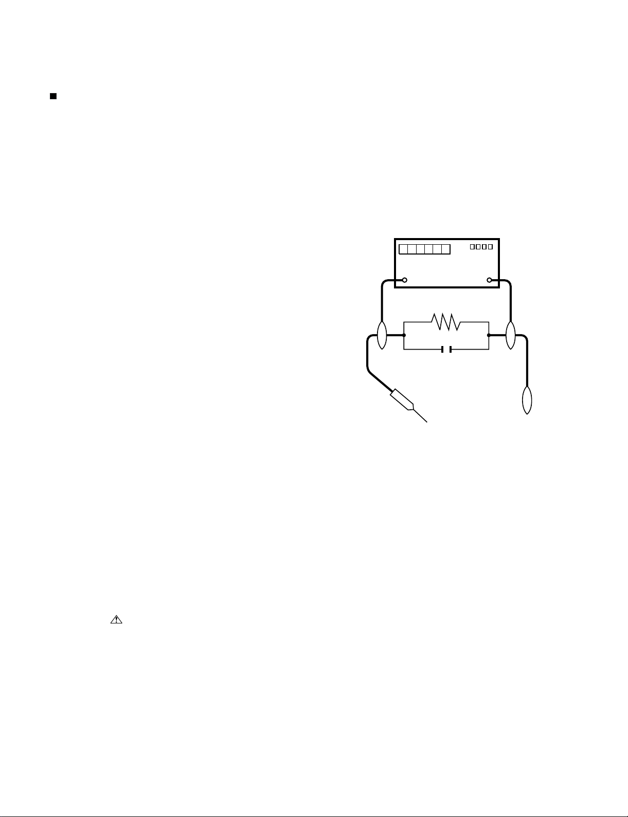
5. To be sure that no shock hazard exists, check for leakage current in
the following manner.
• Plug the AC cord directly into a 110 ~ 240 volt AC outlet.
• Using two clip leads, connect a 1.5k ohm, 10 watt resistor paralleled by a 0.15µF capacitor in series with all exposed metal cabinet
parts and a known earth ground, such as electrical conduit or electrical ground connected to an earth ground.
• Use an AC voltmeter having with 5000 ohm per volt, or higher, sensitivity or measure the AC voltage drop across the resistor.
• Connect the resistor connection to all exposed metal parts having a
return to the chassis (antenna, metal cabinet, screw heads, knobs
and control shafts, escutcheon, etc.) and measure the AC voltage
drop across the resistor.
All checks must be repeated with the AC cord plug connection
reversed. (If necessary, a non polarized adaptor plug must be used
only for the purpose of completing these checks.)
Any reading of 0.74 V rms (this corresponds to 0.5 milliamp. rms
AC.) or more is excessive and indicates a potential shock hazard
which must be corrected before returning the monitor to the owner.
DVM
AC SCALE
1.5k ohm
10W
0.15µF
TEST PROBE
TO EXPOSED
METAL PARTS
CONNECT TO
KNOWN EARTH
GROUND
///////////////////////////////////////////////////////////////////////////////////////////////////////////////////////////////////////////////////////////////////////////////////////////////////////////////////////////////////////////
SAFETY NOTICE
Many electrical and mechanical parts in LCD color television have
special safety-related characteristics.
These characteristics are often not evident from visual inspection, nor
can protection afforded by them be necessarily increased by using
replacement components rated for higher voltage, wattage, etc.
Replacement parts which have these special safety characteristics are
identified in this manual; electrical components having such features
are identified by " " and shaded areas in the Replacement Parts
Lists and Schematic Diagrams.
For continued protection, replacement parts must be identical to those
used in the original circuit.
The use of a substitute replacement parts which do not have the same
safety characteristics as the factory recommended replacement parts
shown in this service manual, may create shock, fire or other hazards.
///////////////////////////////////////////////////////////////////////////////////////////////////////////////////////////////////////////////////////////////////////////////////////////////////////////////////////////////////////////
iii
Page 5
LC-65RX1H/X
Precautions for using lead-free solder
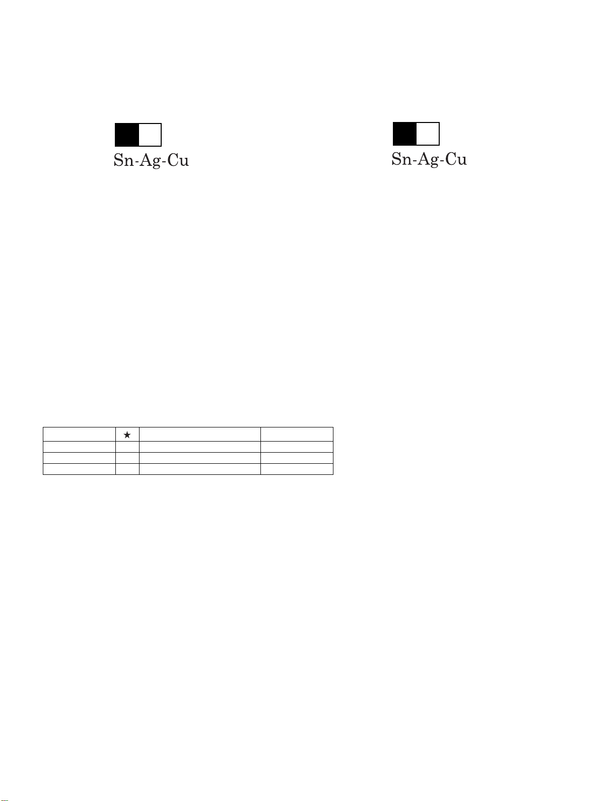
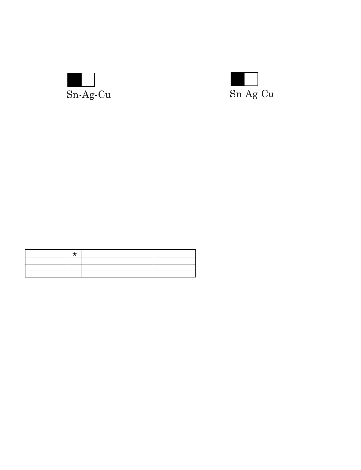
Employing lead-free solder
• “All PWBs” of this model employs lead-free solder. The LF symbol indicates lead-free solder, and is attached on the PWBs and service manuals.
The alphabetical character following LF shows the type of lead-free solder.
Example:
L Fa
Indicates lead-free solder of tin, silver and copper.
Indicates lead-free solder of tin, silver and copper.
L F a/a
Using lead-free wire solder
• When fixing the PWB soldered with the lead-free solder, apply lead-free wire solder. Repairing with conventional lead wire solder may cause damage or accident due to cracks.
As the melting point of lead-free solder (Sn-Ag-Cu) is higher than the lead wire solder by 40 °C, we recommend you to use a dedicated soldering
bit, if you are not familiar with how to obtain lead-free wire solder or soldering bit, contact our service station or service branch in your area.
Soldering
• As the melting point of lead-free solder (Sn-Ag-Cu) is about 220 °C which is higher than the conventional lead solder by 40 °C, and as it has poor
solder wettability, you may be apt to keep the soldering bit in contact with the PWB for extended period of time. However, Since the land may be
peeled off or the maximum heat-resistance temperature of parts may be exceeded, remove the bit from the PWB as soon as you confirm the
steady soldering condition.
Lead-free solder contains more tin, and the end of the soldering bit may be easily corroded. Make sure to turn on and off the power of the bit as
required.
If a different type of solder stays on the tip of the soldering bit, it is alloyed with lead-free solder. Clean the bit after every use of it.
When the tip of the soldering bit is blackened during use, file it with steel wool or fine sandpaper.
• Be careful when replacing parts with polarity indication on the PWB silk.
Lead-free wire solder for servicing
Part No. Description Code
ZHNDAi123250E J φ0.3mm 250g (1roll) BL
ZHNDAi126500E J φ0.6mm 500g (1roll) BK
ZHNDAi12801KE J φ1.0mm 1kg (1roll) BM
iv
Page 6
LC-65RX1H/X
LC65RX1H
CHAPTER 1. SPECIFICATIONS
[1] LC-65RX1H
ServiceManual
Model
Item
LCD panel
Resolution 2,073,600 pixels (1920×1080)
Video Colour System PAL/SECAM/NTSC 3.58/NTSC 4.43/PAL 60
TV Function TV-Standard PAL: B/G, D/K, I SECAM: B/G, D/K, K/K
Receiving
Channel
TV-Tuning System Auto Preset 99 ch
STEREO/BILINGUAL NICAM: B/G, I, D/K A2 stereo: B/G
Brightness 450 cd/m
Viewing angles H : 176º V : 176º
Audio amplifier
Speakers
Terminals
OSD language English/Simplified Chinese/Traditional Chinese/Arabic
Power Requirement AC 110-240 V, 50/60 Hz
Power Consumption 481 W (0.5 W Standby)
Weight without stand 62.0 kg
Operating Temperature 0°C - 40°C
Rear Antenna input
INPUT 1 VIDEO in, AUDIO in, COMPONENT in (480I, 576I, 480P, 576P, 720P/50Hz,
INPUT 2 VIDEO in, AUDIO in, COMPONENT in (480I, 576I, 480P, 576P, 720P/50Hz,
Side INPUT 3 S-VIDEO in, VIDEO in, AUDIO in
INPUT 4
Rear INPUT 5
INPUT 6
INPUT 7 (PC input) 15 pin mini D-sub, AUDIO in (Ø 3.5 mm jack)
MONITOR OUT VIDEO out, AUDIO out
RS-232C 9 pin D-sub male connector
DIGITAL AUDIO OUTPUT
Front Headphone
with stand 66.0 kg
As a part of policy of continuous improvement, SHARP reserves the right to make design and specification changes for
product improvement without prior notice. The performance specification figures indicated are nominal values of production
units. There may be some deviations from these values in individual units.
VHF/UHF 44.25 - 863.25 MHz
CATV S1 - S41ch (including Hyperband)
65" (1639 mm) Advanced Super View & BLACK TFT LCD
2
7.5W x 2 + 15W
10 x 4cm 2pcs, Ø2cm 2pcs, Ø5.5cm 1pc
UHF/VHF 75
720P/60Hz, 1080I/50Hz, 1080I/60Hz)
720P/60Hz, 1080I/50Hz, 1080I/60Hz)
HDMI (HDMI input) (480I, 576I, 480P, 576P, 720P/50Hz, 720P/60Hz, 1080I/50Hz,
1080I/60Hz, 1080P/50Hz, 1080P/60Hz, 1080P/24Hz)
HDMI (HDMI input) (480I, 576I, 480P, 576P, 720P/50Hz, 720P/60Hz, 1080I/50Hz,
1080I/60Hz, 1080P/50Hz, 1080P/60Hz, 1080P/24Hz)
HDMI (HDMI input) (480I, 576I, 480P, 576P, 720P/50Hz, 720P/60Hz, 1080I/50Hz,
1080I/60Hz, 1080P/50Hz, 1080P/60Hz, 1080P/24Hz), AUDIO in (Ø 3.5 mm jack)
Optical Digital Audio output
DIN type
LC-65RX1H
1
,NTSC:M
1 – 1
Page 7
[2] LC-65RX1X
LC-65RX1H/X
Model
Item
LCD panel
Resolution 2,073,600 pixels (1920×1080)
Video Colour System PAL/SECAM/NTSC 3.58/NTSC 4.43/PAL 60
TV Function TV-
Brightness 450 cd/m
Viewing angles H : 176º V : 176º
Audio amplifier
Speakers
Terminals
OSD language English/Simplified Chinese/Traditional Chinese/Arabic
Power Requirement AC 110-240 V, 50/60 Hz
Power Consumption 481 W (0.5 W Standby)*
Weight without stand 62.0 kg
Operating Temperature 0°C - 40°C
As a part of policy of continuous improvement, SHARP reserves the right to make design and specification changes for
product improvement without prior notice. The performance specification figures indicated are nominal values of production
units. There may be some deviations from these values in individual units.
* Standby power consumption is approx. 45W for 15-30 minutes after the TV is turned off by the remote control. This is
required for automatically capturing EPG data for all tuned digital channels.
Standard
Receiving
Channel
TV-Tuning System Auto Preset 99 ch
STEREO/BILINGUAL NICAM: B/G, I, D/K A2 stereo: B/G
Rear Antenna input
INPUT 1 VIDEO in, AUDIO in, COMPONENT in (480I, 576I, 480P, 576P, 720P/50Hz,
INPUT 2 VIDEO in, AUDIO in, COMPONENT in (480I, 576I, 480P, 576P, 720P/50Hz,
Side INPUT 3 S-VIDEO in, VIDEO in, AUDIO in
INPUT 4
Rear INPUT 5
INPUT 6
INPUT 7 (PC input) 15 pin mini D-sub, AUDIO in (Ø 3.5 mm jack)
MONITOR OUT VIDEO out, AUDIO out
RS-232C 9 pin D-sub male connector
DIGITAL AUDIO OUTPUT
Front Headphone
with stand 66.0 kg
Analogue PAL: B/G, D/K, I SECAM: B/G, D/K, K/K
Digital DVB-T
VHF/UHF 44.25 - 863.25 MHz
CATV S1 - S41ch (including Hyperband)
65" (1639 mm) Advanced Super View & BLACK TFT LCD
2
7.5W x 2 + 15W
10 x 4cm 2pcs, Ø2cm 2pcs, Ø5.5cm 1pc
UHF/VHF 75
720P/60Hz, 1080I/50Hz, 1080I/60Hz)
720P/60Hz, 1080I/50Hz, 1080I/60Hz)
HDMI (HDMI input) (480I, 576I, 480P, 576P, 720P/50Hz, 720P/60Hz, 1080I/50Hz,
1080
I/60Hz, 1080P/50Hz, 1080P/60Hz, 1080P/24Hz)
HDMI (HDMI input) (480I, 576I, 480P, 576P, 720P/50Hz, 720P/60Hz, 1080I/50Hz,
1080I/60Hz, 1080P/50Hz, 1080P/60Hz, 1080P/24Hz)
HDMI (HDMI input) (480I, 576I, 480P, 576P, 720P/50Hz, 720P/60Hz, 1080I/50Hz,
1080I/60Hz, 1080P/50Hz, 1080P/60Hz, 1080P/24Hz), AUDIO in (Ø 3.5 mm jack)
Optical Digital Audio output
DIN type
LC-65RX1X
1
1 – 2
Page 8
LC-65RX1H/X
LC65RX1H
CHAPTER 2. OPERATION MANUAL
[1] OPERATION MANUAL
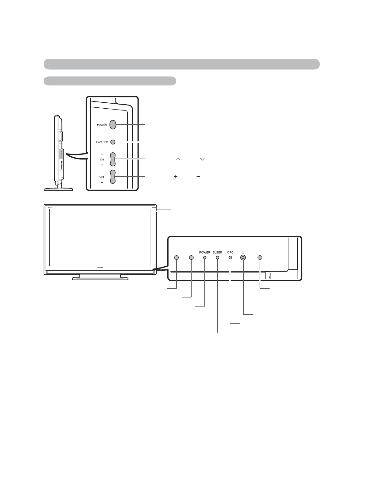
Part names
TV (Front/Side)
POWER (On/Off) button
TV/VIDEO button
Channel up ( )/down ( ) buttons
Volume up ( )/down ( ) buttons
ServiceManual
Remote control sensor
OPC sensor
POWER indicator
Such sensor is not applicable to Hong Kong model.
Such sensor is not applicable
to this model.
Headphone jack
OPC indicator*
SLEEP timer indicator
*OPC: Optical Picture Control
2 – 1
Page 9
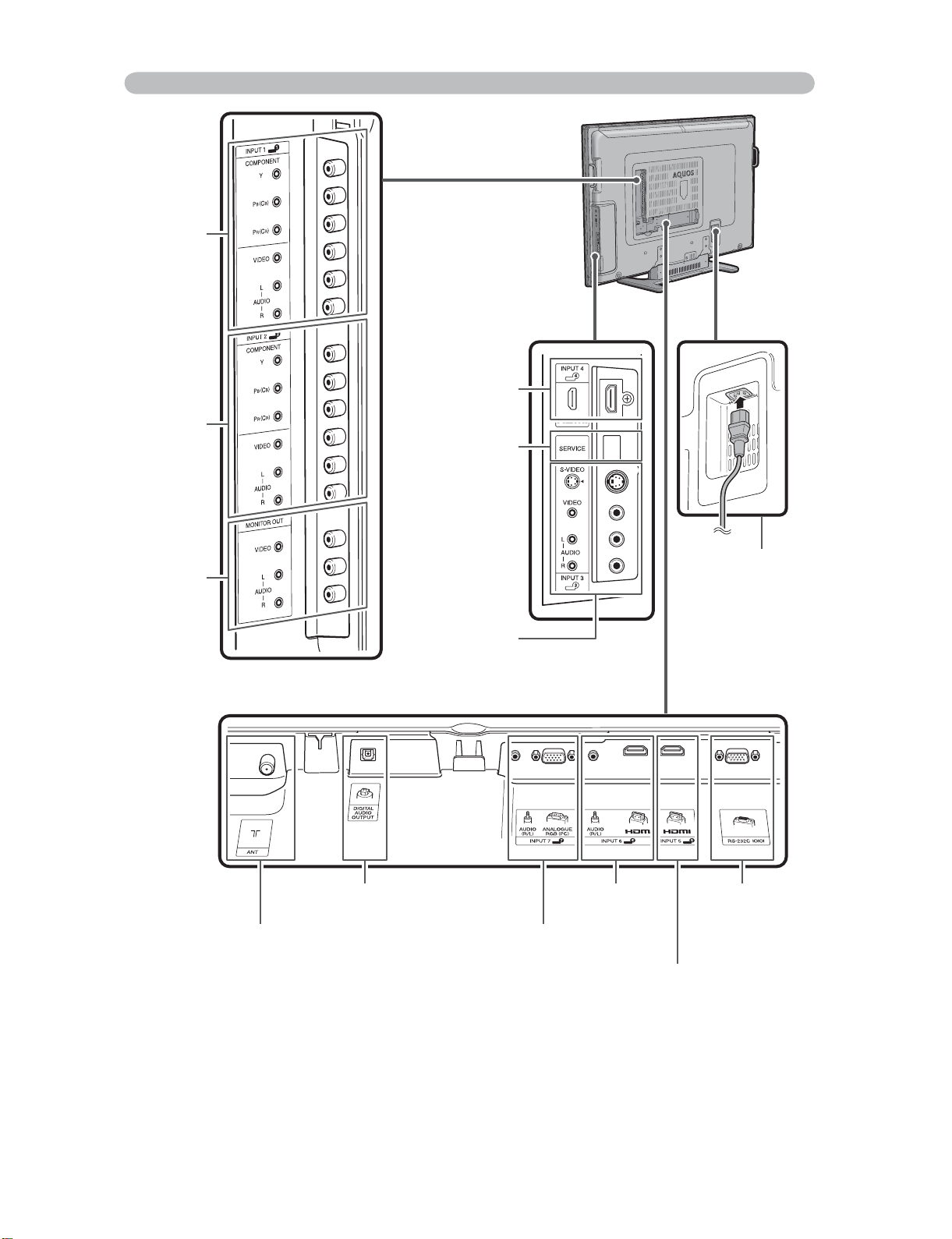
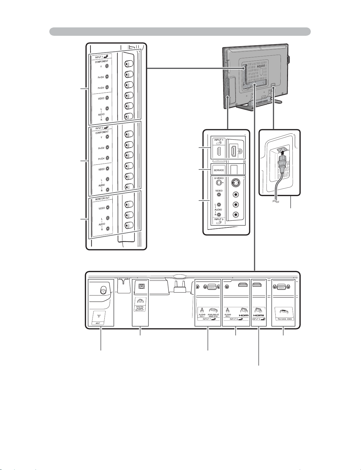
TV (Rear)
INPUT 1
terminals
INPUT 2
terminals
LC-65RX1H/X
INPUT 4 (HDMI)
terminal
SERVICE ONLY
terminal*
MONITOR
OUTPUT
terminals
DIGITAL AUDIO OUTPUT terminal
Antenna input terminal
*
Usuallydo not connect
anything to this terminal
as it is reserved only
for service personnel.
INPUT 3 terminals
INPUT 7 (PC) terminals
INPUT 6 (HDMI)
terminals
AC INPUT terminal
RS-232C terminal
2 – 2
INPUT 5 (HDMI) terminal
Page 10
LC-65RX1H/X
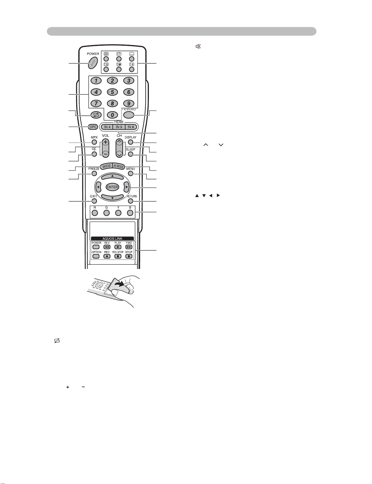
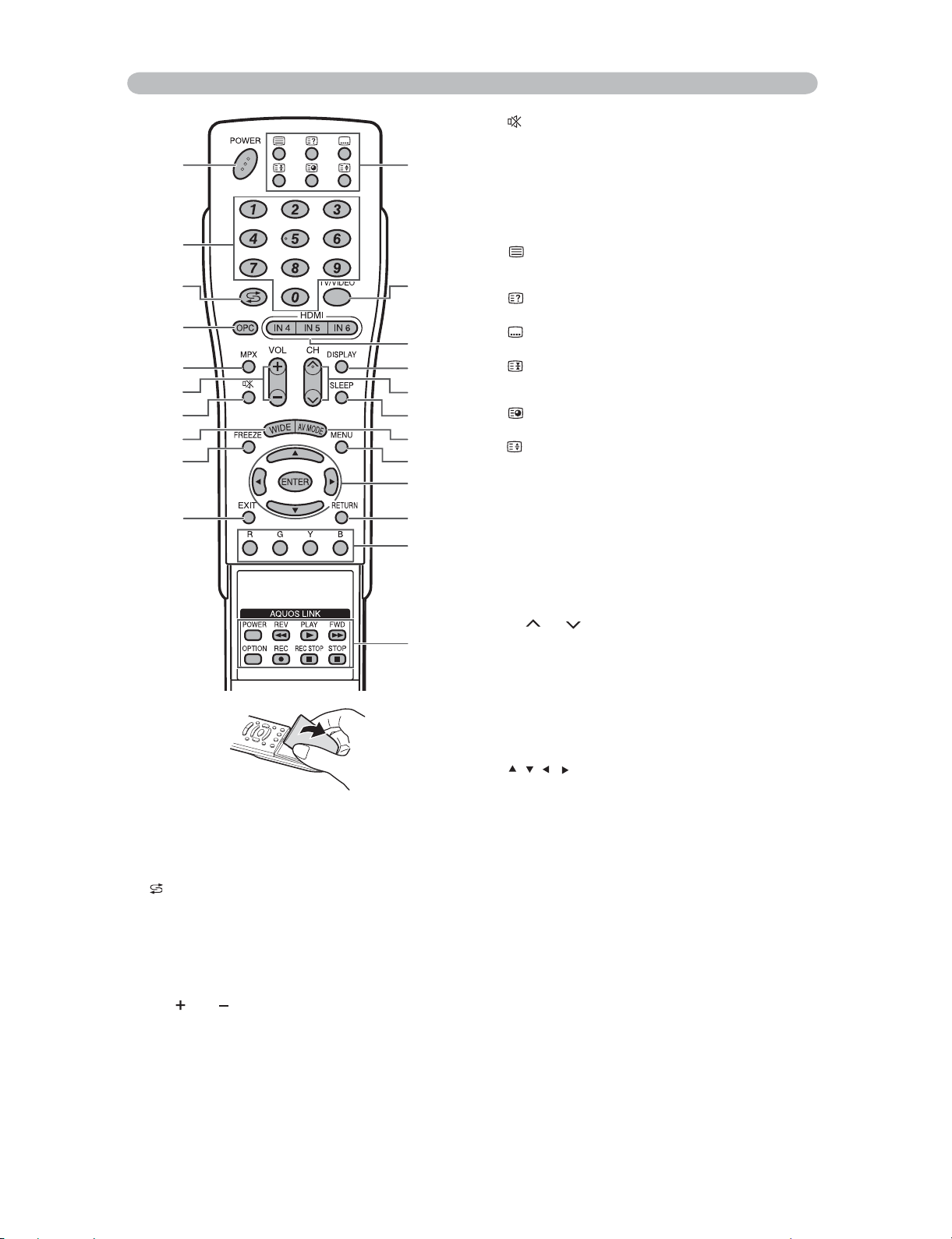
Remote control unit (LC-65RX1H)
1
2
3
4
5
6
7
8
9
10
11
12
13
14
15
16
17
18
19
20
21
22
7 (Mute)
Mute the sound.
8 WIDE
Change the wide image mode.
9 FREEZE
Freeze a motion picture on the screen.
10 EXIT
Turn off the On-Screen Display.
11 Such buttons are not applicable to Hong Kong model.
12 TV/VIDEO (INPUT SOURCE)
Select an input source. (TV, INPUT 1, INPUT 2, INPUT 3,
INPUT 4, INPUT 5, INPUT6, INPUT7 (PC))
13 HDMI
Select an HDMI. (INPUT4, INPUT5, INPUT6)
14 DISPLAY
Displays the channel or input information.
15 CH /CH
TV input mode: Select the channel.
16 SLEEP
Set the Sleep timer.
17 AV MODE
Select a video setting.
18 MENU
Display the menu screen.
19 / / / (Cursor)
Select a desired item on the setting screen.
ENTER
Execute a command.
20 RETURN
MENU mode: Return to the previous menu screen.
21 Such buttons are not applicable to Hong Kong model.
22 AQUOS LINK buttons
If external equipment such as a AQUOS BD Player is
connected via HDMI-certified cables and is AQUOS LINK
compatible, you can use these AQUOS LINK buttons.
1 POWER (STANDBY/ON)
To switch the power on and off.
20-9
Set the channel.
3 (Flashback)
Press to return to the previous selected channel or
external input mode.
4OPC
To switch the Optical Picture Control on and off.
5 MPX
Select the sound multiplex mode.
6 VOL /VOL
Set the volume.
2 – 3
Page 11
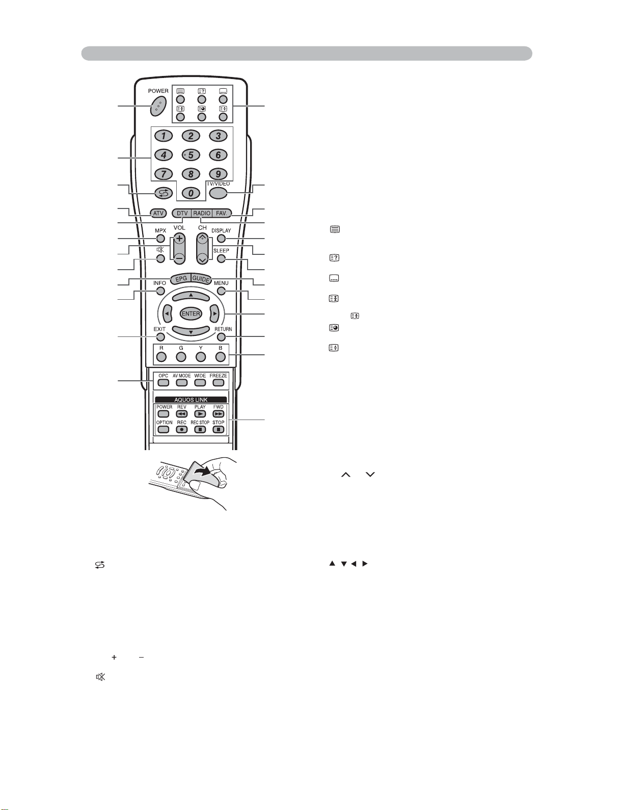
Remote control unit (LC-65RX1X)
1
2
3
4
5
6
7
8
9
10
11
12
1 POWER (STANDBY/ON)
To switch the power on and off.
20-9
Set the channel.
TELETEXT mode: Set the page.
3 (Flashback)
Press to return to the previous selected channel or external
input mode.
4ATV
Press to access ANALOGUE mode.
5DTV
Press to access DTV mode.
6MPX
Select the sound multiplex mode.
7VOL/VOL
Set the volume.
8 (Mute)
Mute the sound.
13
14
15
16
17
18
19
20
21
22
23
24
25
9EPG
DTV only: To display EPG (Electronic Programme Guide)
screen.
10 INFO
DTV only: Display the programme information.
11 EXIT
Turn off the On-Screen Display.
12 OPC
To switch the Optical Picture Control on and off.
AV MODE
Select a video setting.
WIDE
Change the wide image mode.
FREEZE
Freeze a motion picture on the screen.
13 (TELETEXT)
Select the TELETEXT mode. (all TV image, all TEXT image,
TV/TEXT image)
(Reveal hidden for TELETEXT)
TELETEXT mode: Display hidden characters.
(SUBTITLE for TELETEXT)
To turn the subtitles on and off.
(Hold)
TELETEXT mode: Stop updating Teletext pages automatically.
Press again to release the hold mode.
(Subpage)
Display the Teletext subpage directly.
(Top/Bottom/Full)
TELETEXT mode: Set the area of magnification.
14 TV/VIDEO (INPUT SOURCE)
Select an input source. (TV, INPUT 1, INPUT 2, INPUT 3, INPUT 4,
INPUT 5, INPUT6, INPUT7 (PC))
15 FAV.
DTV only: Display the favourite channel setting.
16 RADIO
DTV only: Press to access RADIO mode.
17 DISPLAY
Displays the channel or input information.
Displays the time information included in the Teletext
broadcast.
18 CH /CH
TV input mode: Select the channel.
TELETEXT mode: Select the page.
19 SLEEP
Set the Sleep timer.
20 GUIDE
DTV only: Display the programme list.
21 MENU
Display the menu screen.
22 / / / (Cursor)
Select a desired item on the setting screen.
ENTER
Execute a command.
23 RETURN
MENU mode: Return to the previous menu screen.
24 Colour (Red/Green/Yellow/Blue)
Select four preset favourite channels in four different
categories.
While watching, you can toggle the selected channels by
pressing R, G, Y and B.
TELETEXT mode: Select the page.
25 AQUOS LINK buttons
If external equipment such as a AQUOS BD Player is connected
via HDMI-certified cables and is AQUOS LINK compatible, you can
use these AQUOS LINK buttons.
LC-65RX1H/X
2 – 4
Page 12

LC-65RX1H/X
LC65RX1H
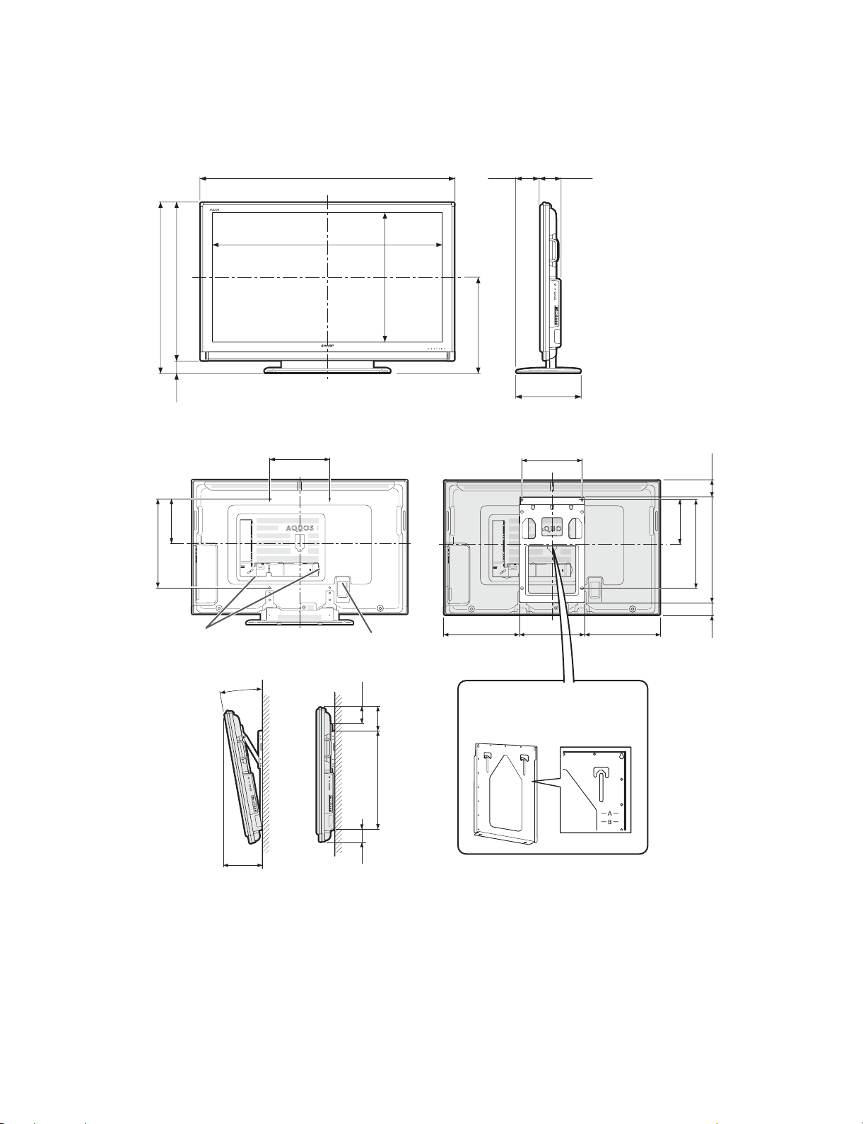
CHAPTER 3. DIMENSIONS
[1] DIMENSIONS
ServiceManual
Unit: mm
1579
1431.5
982
1062
806.5
80
When using wall mount bracket AN-65AG1
440
325
650
597
149
124
398
440
125
325
650
Cable opening
0°/5°/10°
278
Power code
connection terminal
192
18
21
On the wall bracket of AN-65AG1,
there is a letter 'A' indicating the
centre point of the TV monitor.
3 – 1
Page 13
LC65RX1H
CHAPTER 4. TROUBLESHOOTING TABLE
ServiceManual
[1] TROUBLESHOOTING TABLE (for LC-65RX1X)
No picture on the display (3)
Does not the picture come out when DTV is received?
TERMINAL UNIT:
Is the voltage of regulation for a TUNER circuit and the power
supply terminal of IC7507 (COFDM) supplied?
(Refer to the circuit diagram)
YES
Is IF signal output from pin (20), (21) of TUNER (TU7501) to pin
(30), (30) of IC7507 (COFDM)?
TERMINAL UNIT: YES
Similarly, is communication control carried out between pin
(14),(15) of TU7501, and pin (4), (5) of IC7507?
YES
Does X7502 (20.48MHz) oscillate? NO Check X7502 and its peripheral circuits.
NO Each power supply circuit is checked.
NO Check the tuner, IC7507 and their peripheral circuits.
Replace as required.
NO
LC-65RX1H/X
YES
Is MPEG data (FECLK, FED_D, FESTR_PSYNC, FEVAL_DEN)
from IC7507 are output to pin (48)/FECLK, (46)/FED_D, (51)/
FESTR_PSYNC, (50)/FEVAL_DEN of a connector (SC501)?
MAIN UNIT: YES
Is the digital signal input into pin (48)/FECLK, (46)/FED_D, (51)/
FESTR_PSYNC, (50)/FEVAL_DEN of a connector (SC1101)?
YES
Is the digital signal input into pin (AF3)/FECLK, (AF2)/ FED_D,
(AF4)/FESTR_PSYNC, (AH3)/FEVAL_DEN of IC8101 (CPU/
DECODER)?
YES
Do X8101 (24.00MHz)/ X8102 (32.768kMHz) oscillate? NO Check the X8101/ X8102 and their peripheral circuits.
YES
Are video signal VDB_R [0:9], VDB_G [0:9], VDB_B [0:9], and
VBD_CLK/DE/HD/VD are output from IC8101 to IC3301 (VIDEO
PROCESSOR)?
YES
Refer to “The picture doesn't appear in all modes.”
NO Is the control signal named IC7507 and IC9101 (CPLD) normal?
(FE_RST_LINE, FEERR_LINE, FEPG0_COMP_LINE,
FEPG1_LOCK_LINE, etc.)
NO Connector SC501/SC1101 are checked.
NO Check the line between SC1101 and IC8101.
NO Check IC8101, IC3301 and their peripheral circuits.
(IC8301-IC8304 (DDR2_SDRAM), etc.)
4 – 1
Page 14
LC-65RX1H/X
No sound (during the reception of TV (DIGITAL) broadcasting)
Does not the sound go out though the picture has come out when DTV is received?
MAIN UNIT:
Is DTV_SPDIF audio signal output from pin (T2) of IC8101 (CPU/
DECODER) to pin (42) of connector SC1101?
TERMINAL UNIT: YES
Is DTV_SPDIF audio signal input from pin(42) of connector
SC501 to pin(4) of IC1404(CODEC)?
YES
Refer to “No sound output in all modes”.
<During external connection> No picture on the monitor (2)
No picture appears on MONITOR OUT1 - connected monitor during the tuner (DTV) reception.
Checklist:
1) Is ANT-CABLE disconnected or connected improperly? ⋅ ⋅ ⋅ Connect it correctly as per the operation manual.
2) The picture is sent to the monitor in a CVBS signal if the source during display is TV, CVBS or Y/C of INPUT1-3.
When sent by component, etc., that signal is not sent to the monitor.
3) When the monitor picture is not sent and is not displayed on the monitor, refer to “No picture” for each terminal.
NO Check the line between IC8101 and SC1101, and their peripheral
circuits.
NO Check the line between SC501 and IC1404.
(SC1101/SC501, etc.)
TERMINAL UNIT:
Is CVBS signal outputted from pin (51) of IC506 to pin (6) of
J1701?
MAIN UNIT: NO
Is DTV_CVBS signal output from pin (18) of connector (SC1101)
to pin (15) of IC506?
NO
Is DTM_CVBS signal output to pin (AD4) of IC8101? YES Check the line between IC8101 and SC1101.
NO
Check the IC8101 and its peripheral circuits.
YES Check the setting of an external input device that connects of
J1701.
YES Check the line between SC1101 (MAIN_UNIT)/ SC501 (TERMI-
NAL UNIT) and IC506.
4 – 2
Page 15
LC65RX1H
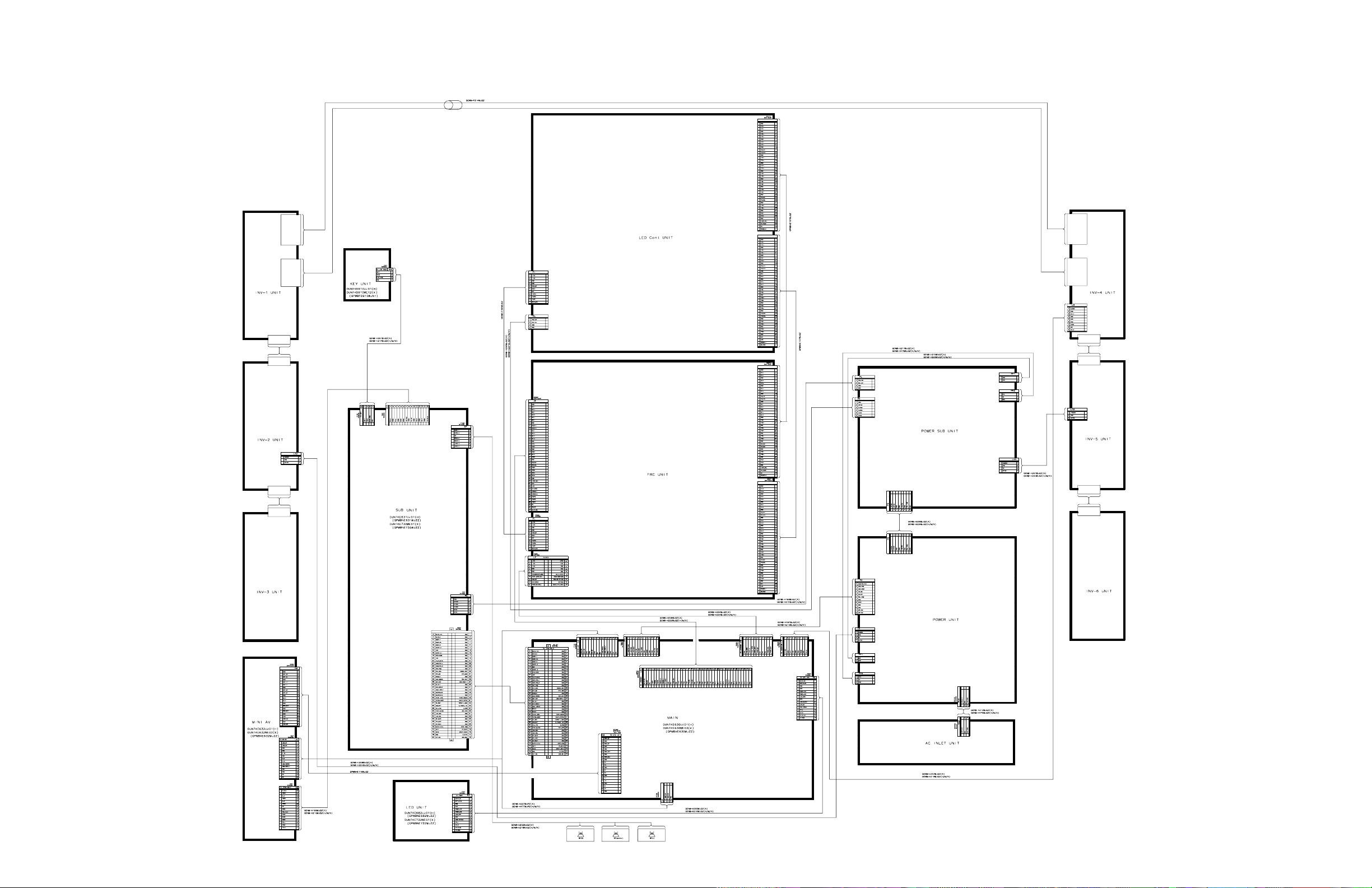
CHAPTER 5. OVERALL WIRING DIAGRAM/BLOCK DIAGLAM
[1] OVERALL WIRING DIAGRAM
LC-65RX1H/X
ServiceManual
5 – 1
Page 16
LC-65RX1H/X
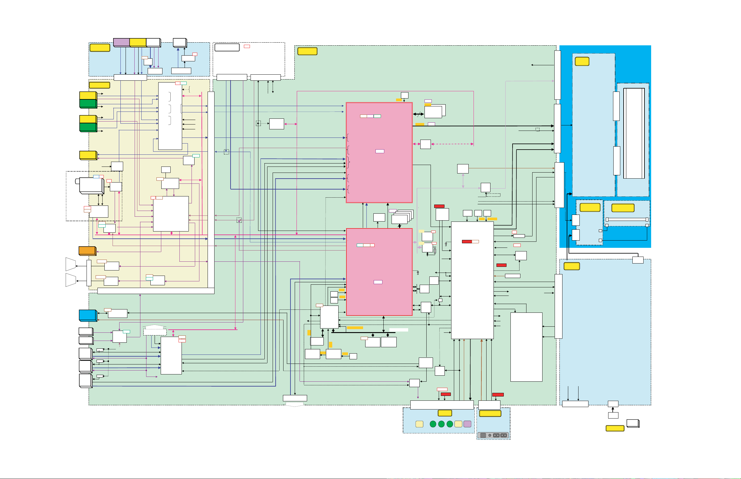
[2] SYSTEM BLOCK DIAGRAM (LC-65RX1X)
58KFGQ
%8$5.4
*&/+
+0276
+0276
/10+614
4(+0
䇼㪪㪧䇽
㪇㪅㪈㪺㪿
+0276
+0276
+0276
+0276
+0276
176
/+0+#8
5;%
+0276+( 22+0
6'4/+0#.
8A2.7)
%8$5.4
;2D2T
%8$5.4
;2D2T
/10+614
176
67
#.25##9,3<
8
8
126+%#.
176
45%
*&+/#WFKQ
/KPK2NWI
2%#WFKQ
/KPK2NWI
*&/+
*&/+
&57$
RKP
%8$5
.4
;2D2T
%1/2A2.7)
8A2.7)
%8$5
.4
;2D2T
%1/2A2.7)
%8$5
.4
+%
㪫㪬㪶㪧㪶㪞㪘㪠㪥
8%#
$##(
8
8
6WPGT
6&3)
%1(&/&GOQF
+PVGN%'
#)%#(6
+%
&A+(
8
8
+%
8
+(
+%
5+(&'%
4#
%8$5
+%
+(&'/1&
6&#
5+(
65A176
㪛㪫㪭㪶㪠㪉㪪
126A176
#/28
+%
#WFKQ#/2
;<
#/28 +%
㪧㪈㪊㪇㪉
+%
㪣㪚㪟
#WFKQ#/2
;<
8
+%
45%6Z4Z
+5.
4%
*&/+A.4
+%
#WFKQ59
2%A.4
0,/
92
''241/
4:AZ
''241/
(TQO%2.&
92
4:AZ
92
''241/
#0#.1)4)$
%8$5
8.4
8A2.7)
5A2.7)
+0276
8
+0A.4
+0A.4
+0A.4
2%*&/+&6/A.4
#0#.1).4
5GTKCN㧕
㪣㪃㪩㪚㪟
+(VQ/#+0+(2+09#9,
.4
8A#
5%
%'%
%'%
*8
4:AZ
%'%
+%
+%
6/&5
*&/+((%
61/#+0
8
+5&52 5&176
8
8
+0
+0
+0
+0
+0
8
8A#
&#%
#-'6
6Z&4Z&
㪝㪝㪚䈪㫄㫀㫅㫀㩷㪘㪭
4:AZ
+%
8KFGQ59+6%*
//:3
8KFGQ
8
;2D2T
8KFGQ
8
;2D2T
8KFGQ
8
;%
6WPGT
8
&KIKVCN
8
+%
''241/
+%
&52
6#5
+5A#
+%
%1&'%
#-'3
6:
126176
.4%-$%-1765&176
+%
*&/+59
8GT
5++#
+P
+P
+P
5'.
6Q/QPKVQT/KEQP
75$
75$A7275$A&0
75$
61/#+0
8A#
8
.
㩰
.
68
/CKP
1WV
176
2.7)
&'6
68
/CKP
1WV
176
/10+614
1768
.4%-$%-1765&176
/10A176
*&/+A52&+(
&68A52&+(
52A176
*2A176
8
8
8$75
+%
40$
888
%1/2
;2D2T
+%
0,/
+5A$
6/&5
4:AZ
/CKP;8
/CKP%
5
#/2
8
+PFWEKPI
FKUVKPEVKQP
UGVVKPI
&6/A%8$5
8A#
&+)+6#.70+6
*&/$6
&6/+( 22+0
&6/A%8$5
+(VQ /#+0 +( 2+0 9# 9,
*&/+A52&+(
&68A52&+(
65
5GTKCN
&68A+5
%-*&8&&'
8
/#+0
&'6A20.8
&6/+( 22+0
5%.5&#
&6/A45
&6/A6:&4:&
%2.&
)2+1A
/CKP;8
/CKP%
+%
5%+5
7#46+%
-*\
;2D2T
*&/+A52&+(
6/&54Z
%-*&8&'0
5%.5&#
*&8&
2%A4)$
;2D2T
6Q%2.&
&68A%8$5
&68A+5
&68A52&+(
%8$5;
%8
5%#46A)8㧕
5%#46A$9
5%#46A4;
($;
;9
2D;
2T9
52&+(9
955&5%-#7&+1%.78;9
2%A4)$*&88&7
2%A47
2%A);
2%A$9
4GUGV(
4Z&6Z&
7#46A#8
+%A
655
*&/+
;;㧕
2D;
2T8
67'4
8
8
8
+%
+:%9,
8KFGQ2TQEGUUGT
5829:
㪩㪼㫍㪅㪚
&+0
2
',6#) ↪
㩄㩒㩂㩊
&A176
$㩘㩩㨺㩎
88
8
&6/A.4
;2D2T
&6/A52&+(
+%
*K&682TQ.:
+:%9,
&KIKVCN#8FGEQFG/CKP%27
)2
75$A7275$A&0
75$A221075$A1%
22+0
75$
㪫㫆㩷㫄㫀㫅㫀㩷㪘㪭
20.A219A/#+0
/*\
2
%QPPGEVQTHQT
%2.&YTKVKPI
+%
+08'46'4
8*%6
8
/*\
+%
%2.&
+:%9,
+:%9,3<
:VCN
-*\
:VCN
/*\
/*\
+%
%.1%-
-*\
/*\
75$
4'5'6
:6.+
:6.1
2%+%.-/*\㧕
/*\
%-
%-'
)2+1
:VCN
/*\
8
%.10'A4%
+%
(.#5*
/DKV
㪩㪼㫍㪅㪚
(.#5*$75
%QPPGEVQTHQT
5QHVYCTGYTKVKPI
$75
$75
5%
/*\
*5/
85/
&2$A%.-4
8
+%
&&4
/DKVZ
5+%A5%.
5+%A5%.
(.#5*2%+$75
/*\
:VCN
:6.+
:6.1
/*\
.8&5176
5%.*
5&#*
DKV
+%A
':'A.'&
)2+1
4Z&6Z&
7#46
4Z&6Z&
7#46
45A$7(A%06
45A6:&4:&
3
ޣ4#ޤ2R0#9,
DKV
-*\
75'4
&6%2
&GDWI
%QPPGEVQT
+%
㪟㪧
8
/*\
'/#$+
2
%JKR
&GDWII GT
%QPPGVQT
+%
''241/
MDKV
+%
''241/
MDKV
92
+%':6
(TQO*&/+
%QPPGE VQTH QT
FKUVKP EVKQP
2
+%
5VCVG
6%9
45A6:&4:&
*2A.4
+%
&&4
/DKV
8
8
8
2
㪦㪧㪚㪪㪣㪜
$78
20.A2192/A4'3
2CKT
2
5RHVYCTGYTKVVKPI
'OWNCVQT
%QPPGEVQT
85;0%
+06
':'A.'&
9#-'A72
%'%A1
%'%A+
25+<A.
25+<A*
#4'#
#4'#
20.6;2'
59
4Z&6Z&
0A54'5'6
+4A2#55
#)%#(6
*2A2.7)
+%
+4A59
5'6
1268
$78
.'&
㪧㪮
㪜㪧
+%
8$46
&#%
/(2
(TQO%2.&
(TQO%2.&
+%
4GUGV
+%
%27
/%
$78 8
+1
+06+
1
+06+
+1
+06+
7#46(QTTGYTKVKPI
7#46
+1
+1
+1
#&
#&
+1
+06
4%
12%
.'&Z
.'&A;1;#-7.'&A12%.'&A4.'&A)
12%
4%
㪦㪧㪚 㪩㪚
/*\
:VCN
+1Z
+%
$7559
97
-*\
:VCN
/*\
#&Z
219A59
-';-';
2R
0#9,
5%.5&#
20.A+%A'0
-*\
+1
+1
+1
+1
+1
+%
+1
#&
+06
+1
+1
+1
+1
+1
+1
+1
+06
+1
+06
56$;A219
$78
ޣ-/ޤ
-';
㪧㫆㫎㪼㫉
㪠㫅㫇㫌㫋㩷 㪪㪼㫃㪼㪺 㫋
㪚㪿㪸㫅㫅㪼 㫃㩷㪪㪼㫃 㪼㪺㫋
㪭㫆㫃㫌㫄㪼
%2.&߆ࠄ
6'/2=?15A5'641/5'.(4#/'
8%1/A92
8
+08A81056$
8$7(
+08A'44'44A20.
8
&'6A2#0.8
+%
''241/
+%A5%.
$4.(
+%A5&#
$78
9A2416A/
356'/2
6JGTOKUVGT
#%A&'6
25A10
#06A219
.0$5*146
&'6A20.8&'6A8&'6A8
&'6A&8&'6A8
&A21945A10.+0-A219'7A2195/219
/76'A#A#..
$CEM7R(CEVKQP
5;0%A&'6
˴$78
$78
&8+#A&'6
/CKP(CEVKQP
˴#8(TQO57$㧕
˴&8
&8A75$
˴&8
˴&8
˴&8
˴&8
&8
˴&6/A8
219'429$
2'
20.8A10
(TQO%2.&
20.A219A/#+0
5%.5&#
4.7&
$78
748
R
ޣ.2ޤ2
ޣ.9ޤ2
R%QCZKCN
8QP
2
ޣ.$ޤ
ޣ2&ޤ21 9'4˴% 106˴22+0
%106
RKP
ޣ.$ޤ
RKP
ޣ.#ޤ
RKP
20.8
219'4
#/28
748
ޣ2#ޤ6Q 6GTO KPCN
R
.%&
+08'46'4
㪠㪥㪭㪜㪩 㪫㪜㪩㩷㪧 㪮㪙
((%
ޣ#%ޤ
R
ޣ#%ޤ
R
#%+0.'6
((%
㧮㧸
QT9CXGNGPIVJ
㪣㪚㪛
㪧㪘㪥㪜㪣
㪈㪐㪉㪇㬍
㪈㪇㪏㪇
ޣ2)ޤ
#%
+0
R
㧦
㧦
8
5 – 2
Page 17
LC65RX1H
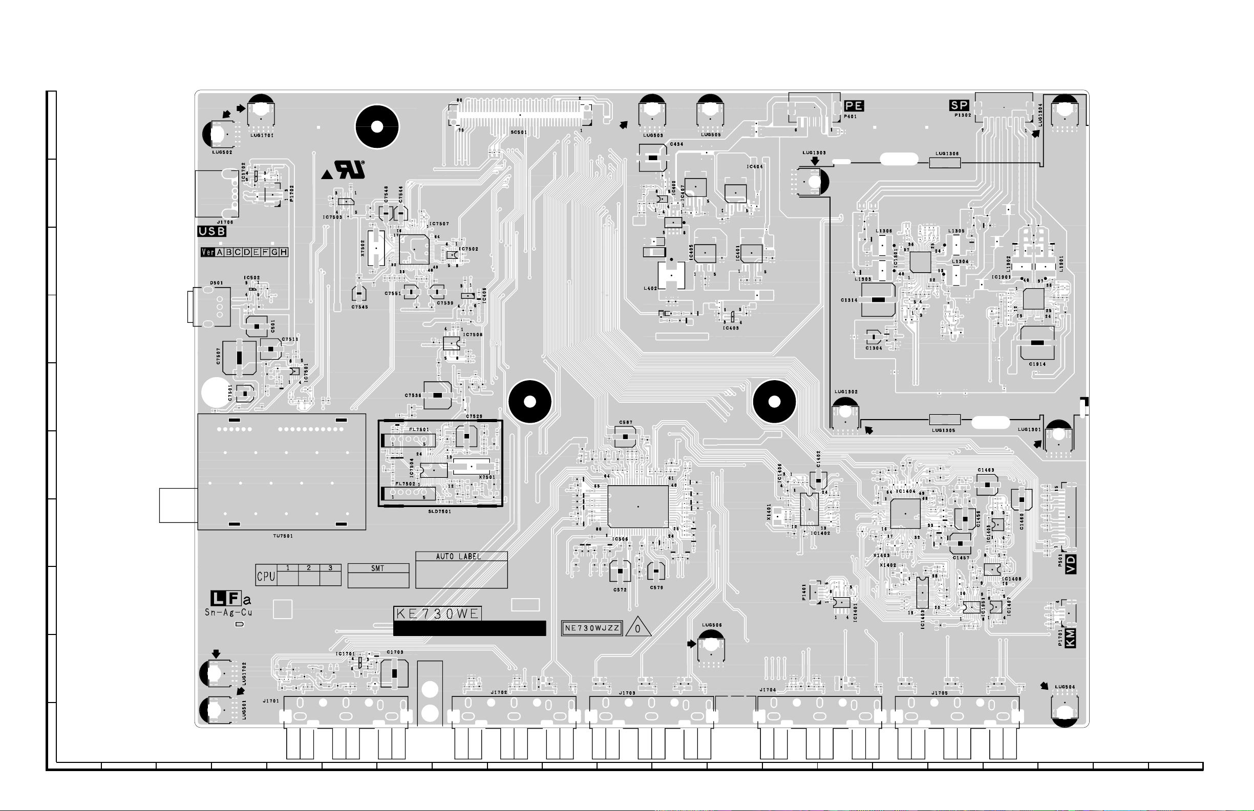
CHAPTER 6. PRINTED WIRING BOARD
[1] SUB UNIT (LC-65RX1X)
Wiring
Side-A
J
I
H
LC-65RX1H/X
ServiceManual
G
F
E
D
C
B
A
123456789
10 11 12 13 14 15 16 17 18 19 20 21
6 – 1
Page 18
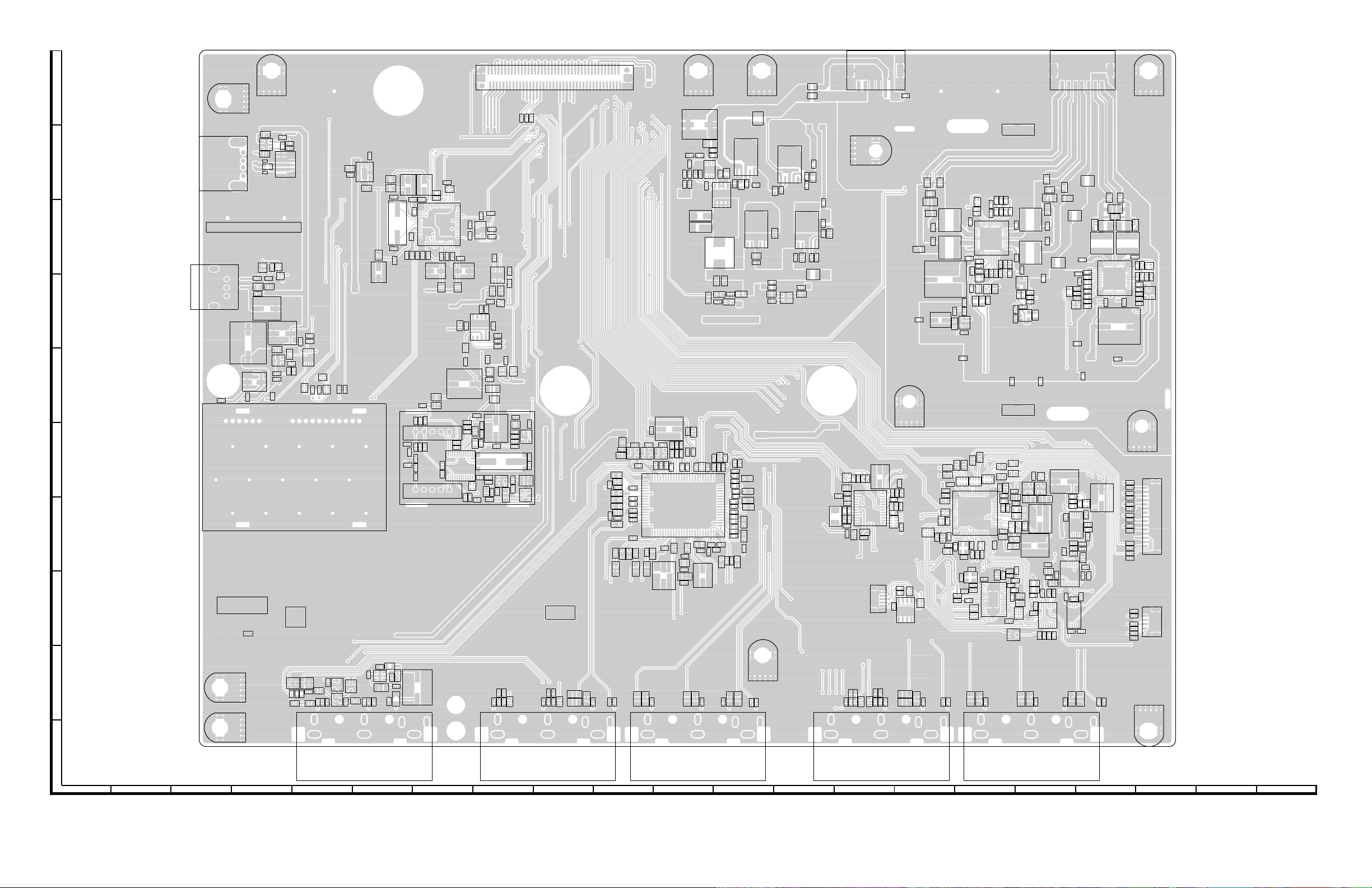
LC-65RX1H/X
Chip Parts
Side-A
J
I
H
G
F
E
D
C
C1403
C1401
C1405
C1407
R1415
C1411C1408
IC1406
R1416R1413
C1412
C1413R1403
R1408
C1410
C1409
LUG1303
R1402
R1409
IC1402
P401
R1329
LUG1306
R1332
R1333
P1401
C1402
R1405
C1450
R1412
R1406
R1959
R1414
C1406
R1417
R1404
R1407
C1451
C1469
R1411
R1438
IC1401
D1305
R1330 C1304
LUG1302
R1419
R1401
R1410
C1326
C1323
D1306
C1320
C1319
C1424
C1314
C1414
R1423
R1420
R1422
C1417
C1425
C1427
C1423
C1421
C1422
R1426
R1421
L1303L1306
R1954
D1302R1309
C1428
C1429
R1436
R1434
R1429
R1310
R1315
C1431
C1420
R1430
Q1303R1308R1313
C1430
X1403
C1317
X1402
C1432
C1419
C1329
C1306
R1338
C1436
R1431
IC1404
R1439
R1440
R1427
R1428
R1446
R1450
R1319
R1317
C1313
C1308
C1311
C1301
R1321
R1305
R1302
R1442
C1438
C1302
R1445
C1437
C1418
R1437
IC1301
C1315
Q1301
R1339
R1320R1325
C1312
R1336C1331
C1309
C1305
R1454
IC1403
C1416
C1307C1332
C1440
C1442
C1444
C1454
R1326R1327
R1455
R1456
C1446
R1312
C1443
C1453
FB1403
C1415
R1337C1328
R1955
C1455
C1426
R1328
R1334R1311
R1314
C1439
C1441
R1453
D1401
D1402
R1435
Q1403
C1447
C1445
D1404
R1433
C1433
C1330
C1316
R1335
R1303
R1304R1307
LUG1305
C1448
C1449
D1403
FB1404
C1434
C1435
R1443
C1327
Q1302
R1322
D1301
FB1401
R1464
C1452
R1907
R1906
R1301
Q1401
L1305
L1304
C1457
C1952
C1951
R1951
C1956
R1418
C1303
R1952
C1456Q1402
R1953
R1331
R1306
D1405
R1462
R1483
C1953
R1958
R1746
R7546
R1745
Q7505
Q7506
R7541
R7573C7581
R1744
SC501
KAME2
R565
L502
R650 R661
C617
Q516
C1745
D550
R612
C600
R610
R616
D546
R537
D545
R644
D543
C589
R599
C593
R536
R595
R643
D541
R535
D531
D532
R575C580
C587
R671
Q520
Q518
R670
R660
R649
R618
C575
D530
R569C571
R574C574
C572
LUG1701
LUG502
C1749
R1740
R1739
R1743
IC1702
C1748
C1747
P1702
VA1702
J1706
D501
C7510
L1701
VA1701
KU3
Q521
R534
IC502
D521
C525
R503
L501
C518
C502
C501
C7511
R7505
C7503
FB7501
Q7501
C7508
R7509
C7502
R7502
R7504
TU7501
D7501
KAME1
R7568
R7501
IC7501
C7505
R7527
C7506
R7564
C7507
C7501
C7504
C7509
KU2
KAME5
C7514
C7522
R7547
C7521
IC7503
C7580
C7526
C7545L7506
L7509
L7510
C7560
C7561
C7553
X7502
R7517
R7512
C7548
C7565
C7554
C7516
C7563
C7564
C7557
R7519
D7503
C7519R7530R7506
C7566
C7552
C7515
D7505
D7504
C7544
C7567
R7518
D7506
C7556
FL7501
FL7502
C7518
C7520
C7551
L7502
C7517
IC7507
R7516
L7511
C7523R7521
R7567
R7566
R7508
C7568
C7524
R7520
C7540
L7504
C7539
C7573
C7536
SLD7501
IC7504
C7577
R7534C7575
C7525
R7522
C7528
C7533
R7570R7572
R7524
R7528
R7523
C7532
C7538
C7530
R7538
R7569
IC7502
R7549
IC7508
R7526C7535
C7542
C7574
R7510
R7548
C7541
R7533
C7550
C7547
R7571
C7513
R438
IC7506
R7525
C433
C7572
L7503
R7539
C431
C7576
R7552
R7550
R7529
IC406
C7529
R7536
FB7502
C426
Q407
X7501
Q7504
Q7507
R7551
R7540
C428
D408
Q7502
C7537
L7505
C7543
R7537
C7527
R7535
R7544R7545
LUG503
C434
C414
C411
C406
C405
R415
IC402
C407
R420
C408
R408R409R410
R402C402
R566
R623C608
R622C611
R673C632
C602
C601
R619R625
IC506
C578
C577
C506
L503
C503
R501
C505
FB402
R423
Q402
D405
D402
L402
C417
C420
D410
R432 D411 C404
D409
R433
D412
C588
R621
C615
FB519
R628
R540
R614
R615C610
C603
C604
R582
R652
D529
R646
R580
R571
R572
D533
C579
LUG505
R445
IC407
R442
C436
C435
R443
IC405
C429
C430
R401
R403
C403
R538
R539
R613
R609
D548
R606
R608
D544
R600
R604
D542
R596
R598
D534
R592
R591
R589
R587
R656
R657
R586D537D536
R570
D535
FB405
FB406
FB404
IC404
C422
R431R430
C423
C424
R502
R405FB403
C409
IC401
C432
R407
R406
C410
C412
R404
FB401
C401
IC403
C1404
X1401
R1324
C1322
C1324
C1473
R1478
D1303
C1318C1321
C1954
C1955
IC1951
R1957
R1424
R1956
R439
R1479
C1463
R1323
D1304
R1473
C1462
C1470
R1476
C1901
R1472
R1468
C1459
IC1408
R441
C1461
R1469
R1482
R1475
R1901
R1908
R1927
Q1902
R1903
IC1407
C1907
IC1405
R1477
P1302
C1916
C1904
R1466
R1463
R1467
R1905
C1472
R1481
C1471
R1474
R440
C1911
C1909
C1913
C1910
C1902
R1911
R1910
R1925
R1470
R1465
R1461
C1458
R1460
R1480
D1903
L1902
C1921
C1460
C1915
R1923
C1924
C1923
IC1901
R1902
C1914
R1924
C1922
L1901
C1918
FB524
C629
FB523
C628
FB522
C627
FB521
C626
FB520
C625
FB509
C623
FB518
C624
C1917
C1743
FB1704
FB1703
C1744
FB1702
C1746
D1904
R1914
R1917
C1919
R1929
C1920
R1921
R1922
R1916
R1928
LUG1301
R1918
R1920
LUG1304
R1919
Q1901
P501
P1701
FB1701
C1711
C1717
D1701
R1705
R1736
D1702
C1719
J1701
R1718
C1708
R1708
IC1701
C1718
R1702
R1710
R1701
C1703
R1729
B
LUG1702
LUG501
Q1703
R1728
C1726
R1738
R1737
Q1704
R1727
C1720
C1725
R1717
C1714
R1709
Q1701
Q1702
A
123456789
C1709
R1712R1726
R1735C1730
C1732
C1704
J1702
R1711C1724
R1734R1722
C1731
R1742
C1733
R1703
LUG506
C1702
C1716
R1713
C1734
R1730
C1727
C1735
J1703
R1723
C1721
C1712
R1719
C1736
C1706
R1707
C1710
R1716R1725
R1733C1729
C1738
C1737
R1732R1721
J1704
R1714C1723
C1705
R1741
C1739
R1704
C1701
C1715
R1715
C1740
R1731
C1728
C1741
J1705
R1724
C1722
C1713
R1720
C1742
R1706
C1707
LUG504
10 11 12 13 14 15 16 17 18 19 20 21
6 – 2
Page 19
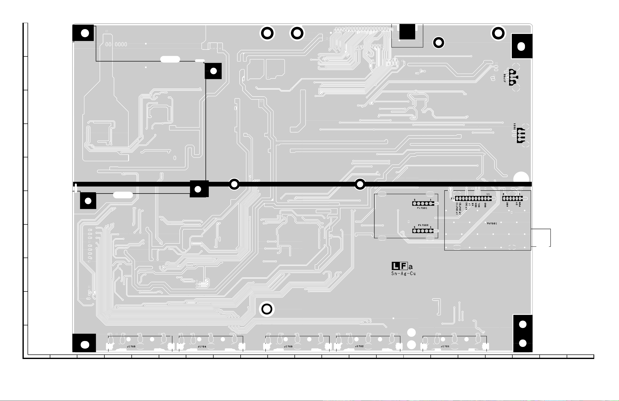
J
I
H
G
LC-65RX1H/X
Wiring
Side-B
F
E
D
C
B
A
123456789
10 11 12 13 14 15 16 17 18 19 20 21
6 – 3
Page 20

LC-65RX1H/X
LC65RX1H
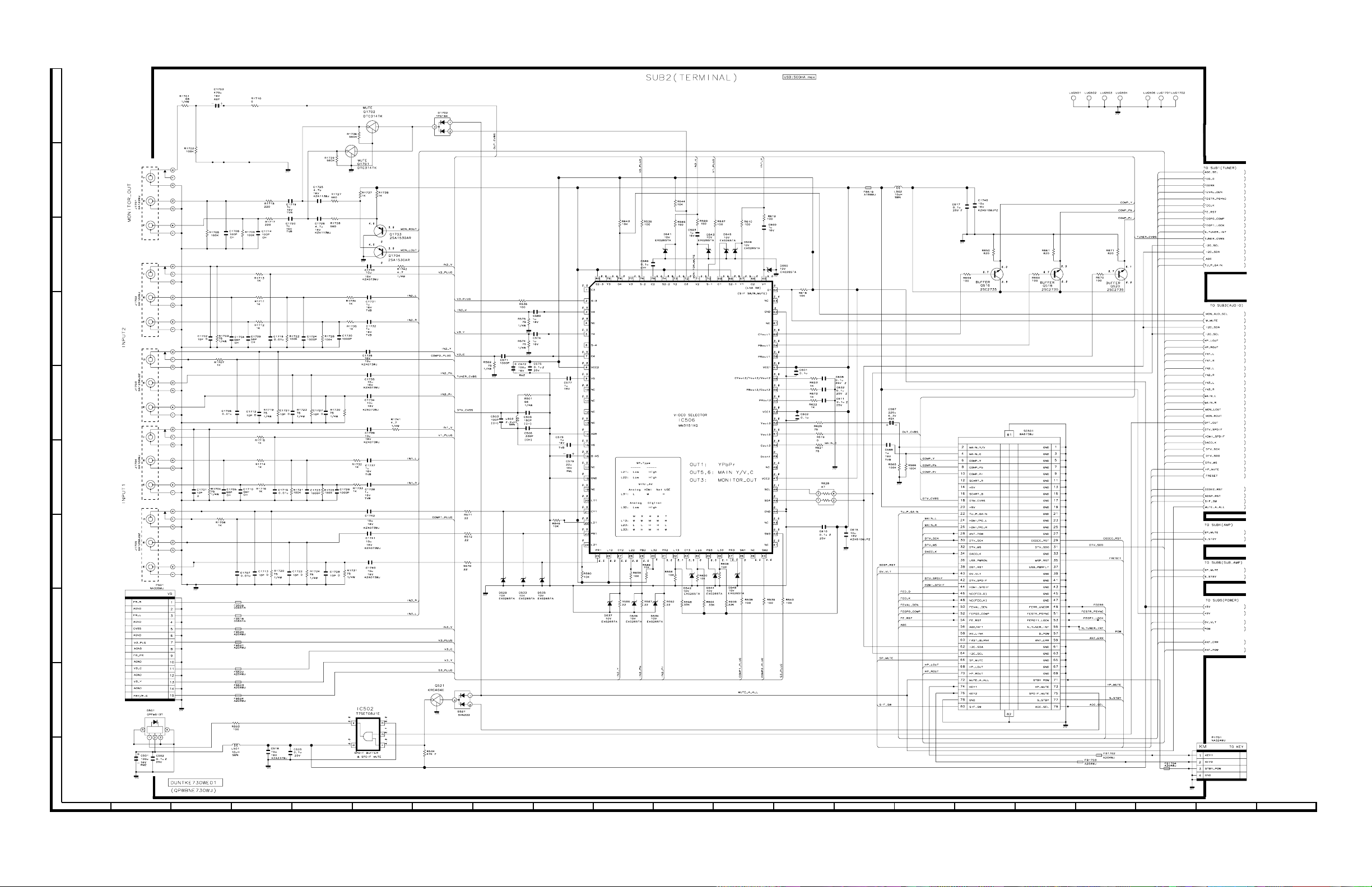
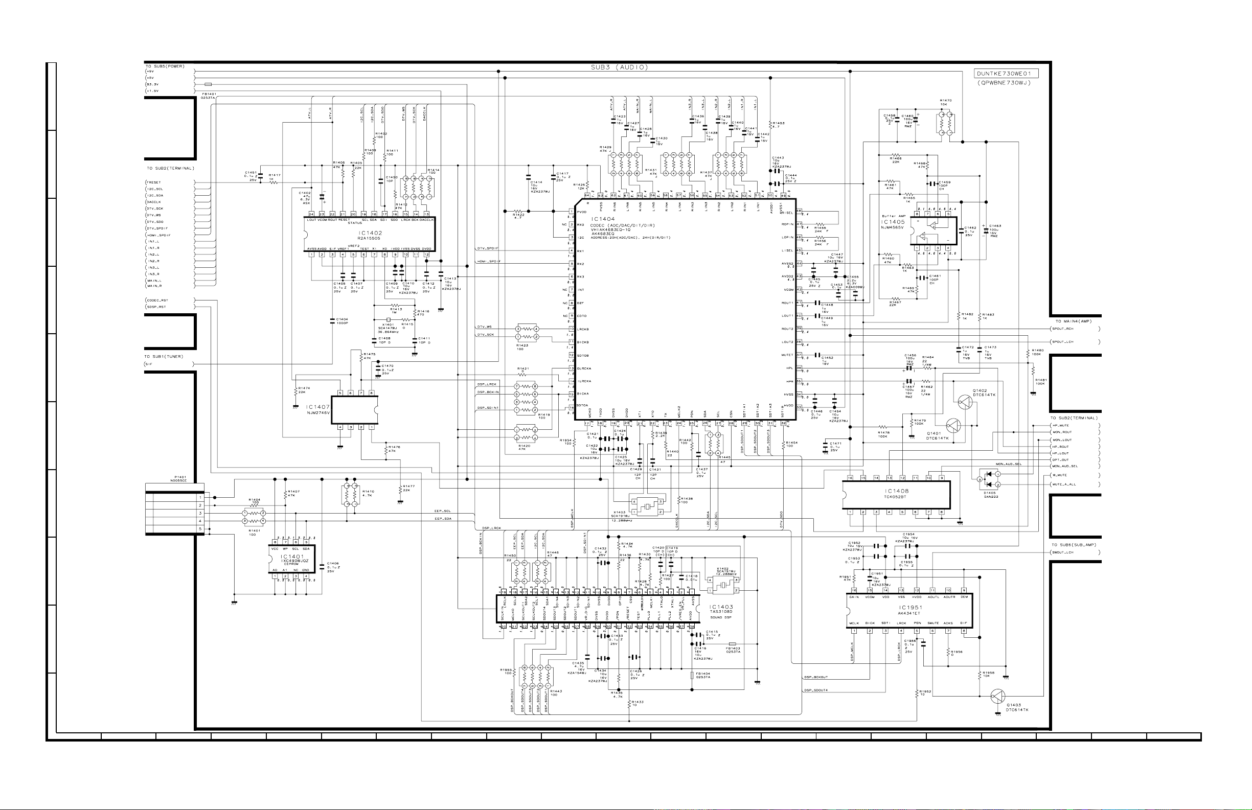
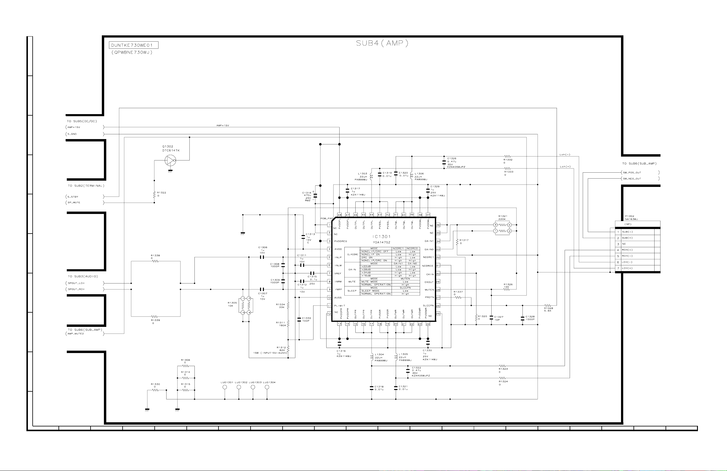
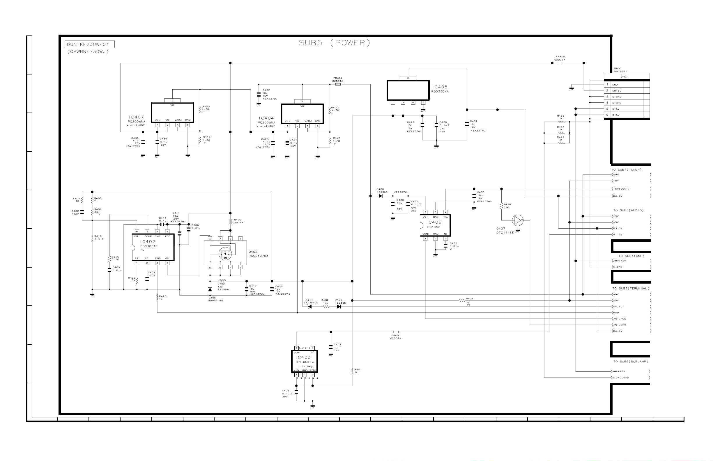
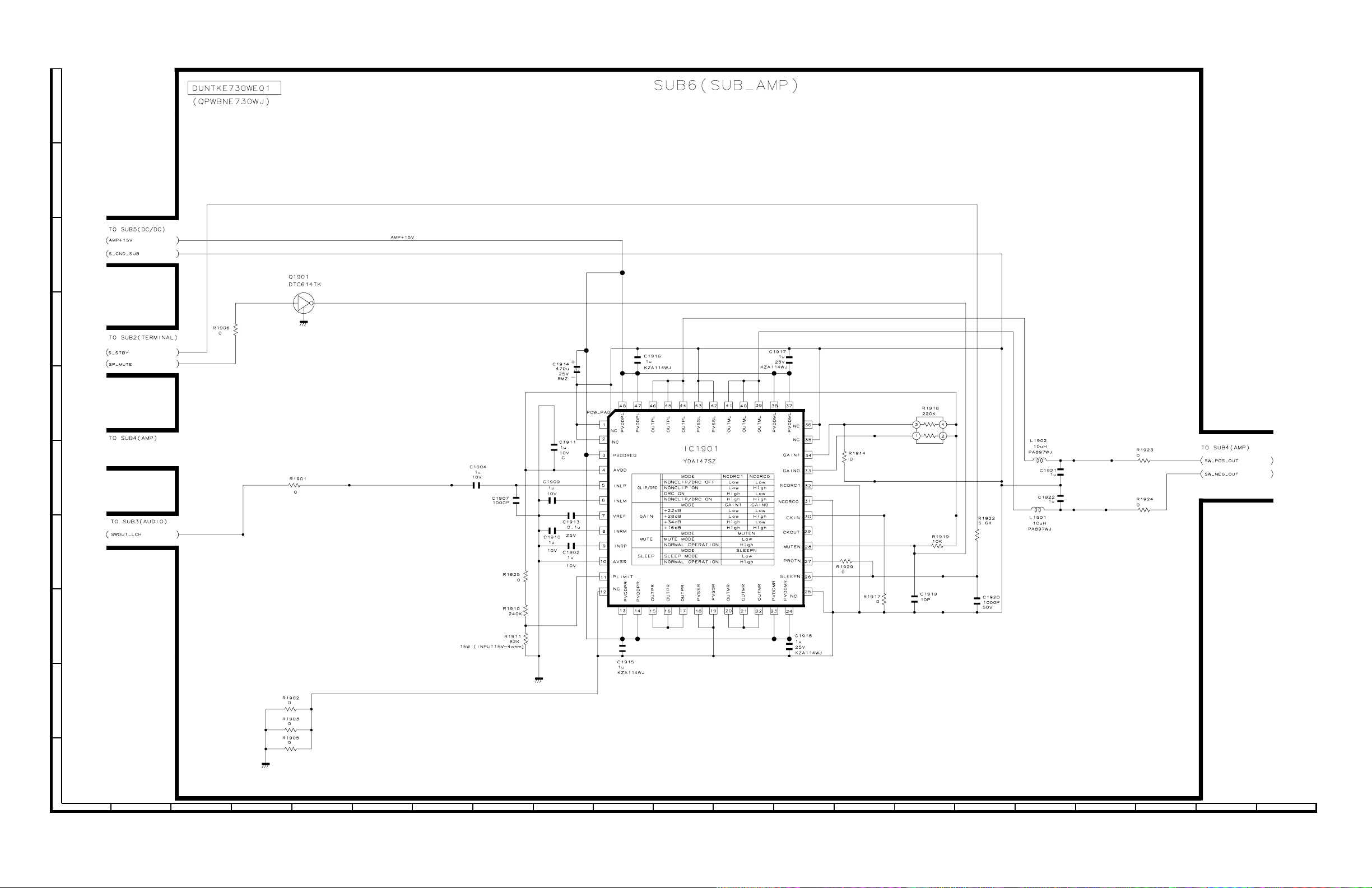
CHAPTER 7. SCHEMATIC DIAGRAM
[1] SCHEMATIC DIAGRAM (LC-65RX1X)
1. DESCRIPTION OF SCEMATIC DIAGRAM
ServiceManual
7 – 1
Page 21

2. SUB UNIT-1
J
I
H
G
LC-65RX1H/X
F
E
D
C
B
A
123456789
10 11 12 13 14 15 16 17 18 19 20 21
7 – 2
Page 22
LC-65RX1H/X
3. SUB UNIT-2
J
I
H
G
F
E
D
C
B
A
123456789
10 11 12 13 14 15 16 17 18 19 20 21
7 – 3
Page 23
4. SUB UNIT-3
J
I
H
G
LC-65RX1H/X
F
E
D
C
B
A
123456789
10 11 12 13 14 15 16 17 18 19 20 21
7 – 4
Page 24
LC-65RX1H/X
5. SUB UNIT-4
J
I
H
G
F
E
D
C
B
A
123456789
10 11 12 13 14 15 16 17 18 19 20 21
7 – 5
Page 25
6. SUB UNIT-5
J
I
H
G
LC-65RX1H/X
F
E
D
C
B
A
123456789
10 11 12 13 14 15 16 17 18 19 20 21
7 – 6
Page 26
LC-65RX1H/X
7. SUB UNIT-6
J
I
H
G
F
E
D
C
B
A
123456789
10 11 12 13 14 15 16 17 18 19 20 21
7 – 7
Page 27

TopPage
LC-65RX1M
SERVICE MANUAL
No. S58K6LC65RX1M
LCD COLOR TELEVISION
MODEL
In the interests of user safety (required by safety regulations in some countries) the set should be restor ed to its
original condition and only parts identical to those specified should be used.
LC-65RX1M
CONTENTS
SAFETY PRECAUTION
IMPORTANT SAFETY PRECAUTION................i
Precautions for using lead-free solder ...............ii
CHAPTER 1. SPECIFICATIONS
[1] SPECIFICATIONS ......................................... 1-1
CHAPTER 2. OPERATION MANUAL
[1] OPERATION MANUAL..................................2-1
CHAPTER 3. DIMENSIONS
[1] DIMENSIONS ................................................ 3-1
CHAPTER 4. REMOVING OF MAJOR PARTS
[1] REMOVING OF STAND AND CABINET........4-1
[2] REMOVING OF MAJOR PARTS FROM
PANEL UNIT .................... ... .... ... ... ... .... .......... 4-2
[3] REMOVING OF MAJOR PARTS FROM
CHASSIS TRAY.............................................4-6
CHAPTER 5. ADJUSTMENT PROCEDURE
[1] ADJUSTMENT PROCEDURE.......................5-1
CHAPTER 6. TROUBLESHOOTING TABLE
[1] TROUBLESHOOTING TABLE ......................6-1
CHAPTER 7. MAJOR IC INFORMATIONS
[1] MAJOR IC INFORMATIONS.........................7-1
CHAPTER 8. BLOCK DIAGRAM/OVERALL WIRING
DIAGRAM
[1] SYSTEM BLOCK DIAGRAM..... .... ... ... ... .... ...8-1
[2] OVERALL WIRING DIAGRAM......................8-2
CHAPTER 9. PRINTED WIRING BOARD
[1] MAIN UNIT ....................................................9-1
[2] SUB UNIT......................................................9-5
[3] FRC UNIT......................................................9-8
[4] MINI-AV UNIT..............................................9-12
[5] R/C, LED/KEY UNIT....................................9-13
CHAPTER 10. SCHEMATIC DIAGRAM
[1] SCHEMATIC DIAGRAM..............................10-1
Parts Guide
Parts marked with " " are important for maintaining the safety of the set. Be sure to replace these parts with specified ones for maintaining the
safety and performance of the set.
This document has been published to be used for
after sales service only.
The contents are subject to change without notice.
Page 28
LC-65RX1M
LC65RX1M
SAFETY PRECAUTION
ServiceManual
IMPORTANT SAFETY PRECAUTION
Service work should be performed only by qualified service technicians who are thoroughly familiar with all safety checks and the
servicing guidelines which follow:
WARNING
1. For continued safety, no modification of any circuits should be
attempted.
2. Disconnect AC power before servicing.
BEFORE RETURNING THE RECEIVER
(Fire & Shock Hazard)
Before returning the receiver to the user, perform the following
safety checks:
3. Inspect all lead dress to make certain that leads are not pinched,
and check that hardware is not lodged between the chassis and
other metal parts in the receiver.
4. Inspect all protective devices such as non-metallic control knobs,
insulation materials, cabinet backs, adjustment and compartment
covers or shields, isolation resistor-capacitor networks, mechanical
insulators, etc.
5. To be sure that no shock hazard exists, check for leakage current in
the following manner.
• Plug the AC cord directly into a 110 ~ 240 volt AC outlet.
• Using two clip leads, connect a 1.5k ohm, 10 watt resistor paralleled by a 0.15µF capacitor in series with all exposed metal cabinet
parts and a known earth ground, such as electrical conduit or electrical ground connected to an earth ground.
• Use an AC voltmeter having with 5000 ohm per volt, or higher, sensitivity or measure the AC voltage drop across the resistor.
• Connect the resistor connection to all exposed metal parts having a
return to the chassis (antenna, metal cabinet, screw heads, knobs
and control shafts, escutcheon, etc.) and measure the AC voltage
drop across the resistor.
All checks must be repeated with the AC cord plug connection
reversed. (If necessary, a non polarized adaptor plug must be used
only for the purpose of completing these checks.)
Any reading of 0.74 V rms (this corresponds to 0.5 milliamp. rms
AC.) or more is excessive and indicates a potential shock hazard
which must be corrected before returning the monitor to the owner.
DVM
AC SCALE
1.5k ohm
10W
0.15µF
TEST PROBE
TO EXPOSED
METAL PARTS
CONNECT TO
KNOWN EARTH
GROUND
///////////////////////////////////////////////////////////////////////////////////////////////////////////////////////////////////////////////////////////////////////////////////////////////////////////////////////////////////////////
SAFETY NOTICE
Many electrical and mechanical parts in LCD color television have
special safety-related characteristics.
These characteristics are often not evident from visual inspection, nor
can protection afforded by them be necessarily increased by using
replacement components rated for higher voltage, wattage, etc.
Replacement parts which have these special safety characteristics are
identified in this manual; electrical components having such features
are identified by " " and shaded areas in the Replacement Parts
Lists and Schematic Diagrams.
For continued protection, replacement parts must be identical to those
used in the original circuit.
The use of a substitute replacement parts which do not have the same
safety characteristics as the factory recommended replacement parts
shown in this service manual, may create shock, fire or other hazards.
///////////////////////////////////////////////////////////////////////////////////////////////////////////////////////////////////////////////////////////////////////////////////////////////////////////////////////////////////////////
i
Page 29
LC-65RX1M
Precautions for using lead-free solder
Employing lead-free solder
• “All PWBs” of this model employs lead-free solder. The LF symbol indicates lead-free solder, and is attached on the PWBs and service manuals.
The alphabetical character following LF shows the type of lead-free solder.
Example:
L Fa
Indicates lead-free solder of tin, silver and copper.
Indicates lead-free solder of tin, silver and copper.
L F a/a
Using lead-free wire solder
• When fixing the PWB soldered with the lead-free solder, apply lead-free wire solder. Repairing with conventional lead wire solder may cause damage or accident due to cracks.
As the melting point of lead-free solder (Sn-Ag-Cu) is higher than the lead wire solder by 40 °C, we recommend you to use a dedicated soldering
bit, if you are not familiar with how to obtain lead-free wire solder or soldering bit, contact our service station or service branch in your area.
Soldering
• As the melting point of lead-free solder (Sn-Ag-Cu) is about 220 °C which is higher than the conventional lead solder by 40 °C, and as it has poor
solder wettability, you may be apt to keep the soldering bit in contact with the PWB for extended period of time. However, Since the land may be
peeled off or the maximum heat-resistance temperature of parts may be exceeded, remove the bit from the PWB as soon as you confirm the
steady soldering condition.
Lead-free solder contains more tin, and the end of the soldering bit may be easily corroded. Make sure to turn on and off the power of the bit as
required.
If a different type of solder stays on the tip of the soldering bit, it is alloyed with lead-free solder. Clean the bit after every use of it.
When the tip of the soldering bit is blackened during use, file it with steel wool or fine sandpaper.
• Be careful when replacing parts with polarity indication on the PWB silk.
Lead-free wire solder for servicing
Part No. Description Code
ZHNDAi123250E J φ0.3mm 250g (1roll) BL
ZHNDAi126500E J φ0.6mm 500g (1roll) BK
ZHNDAi12801KE J φ1.0mm 1kg (1roll) BM
ii
Page 30
LC-65RX1M
LC65RX1M
CHAPTER 1. SPECIFICATIONS
[1] SPECIFICATIONS
ServiceManual
Model
Item
LCD panel
Resolution 2,073,600 pixels (1920×1080)
Video Colour System PAL/SECAM/NTSC 3.58/NTSC 4.43/PAL 60
TV Function TV-Standard PAL: B/G, D/K, I SECAM: B/G, D/K, K/K
Receiving
Channel
TV-Tuning System Auto Preset 99 ch
STEREO/BILINGUAL NICAM: B/G, I, D/K A2 stereo: B/G
Brightness 450 cd/m
Viewing angles H : 176º V : 176º
Audio amplifier
Speakers
Terminals
OSD language English/Simplified Chinese/Traditional Chinese/Arabic
Power Requirement AC 110-240 V 50/60 Hz
Power Consumption 481 W (0.5 W Standby)
Weight without stand 62.0 kg
Operating Temperature 0°C - 40°C
Rear Antenna input
INPUT 1 VIDEO in, AUDIO in, COMPONENT in (480I, 576I, 480P, 576P, 720P/50Hz,
INPUT 2 VIDEO in, AUDIO in, COMPONENT in (480I, 576I, 480P, 576P, 720P/50Hz,
Side INPUT 3 S-VIDEO in, VIDEO in, AUDIO in
INPUT 4
Rear INPUT 5
INPUT 6
INPUT 7 (PC input) 15 pin mini D-sub, AUDIO in (Ø 3.5 mm jack)
MONITOR OUT VIDEO out, AUDIO out
RS-232C 9 pin D-sub male connector
DIGITAL AUDIO OUTPUT
Front Headphone
with stand 66.0 kg
As a part of policy of continuous improvement, SHARP reserves the right to make design and specification changes for
product improvement without prior notice. The performance specification figures indicated are nominal values of production
units. There may be some deviations from these values in individual units.
VHF/UHF 44.25 - 863.25 MHz
CATV S1 - S41ch (including Hyperband)
65" (1639 mm) Advanced Super View & BLACK TFT LCD
2
7.5W X 2 + 15W
10 X 4cm 2pcs, Ø2cm 2pcs, Ø5.5cm 1pc
UHF/VHF 75
720P/60Hz, 1080I/50Hz, 1080I/60Hz)
720P/60Hz, 1080I/50Hz, 1080I/60Hz)
HDMI (HDMI input) (480I, 576I, 480P, 576P, 720P/50Hz, 720P/60Hz, 1080I/50Hz,
1080I/60Hz, 1080P/50Hz, 1080P/60Hz, 1080P/24Hz)
HDMI (HDMI input) (480I, 576I, 480P, 576P, 720P/50Hz, 720P/60Hz, 1080I/50Hz,
1080I/60Hz, 1080P/50Hz, 1080P/60Hz, 1080P/24Hz)
HDMI (HDMI input) (480I, 576I, 480P, 576P, 720P/50Hz, 720P/60Hz, 1080I/50Hz,
1080
I/60Hz, 1080P/50Hz, 1080P/60Hz, 1080P/24Hz), AUDIO in (Ø 3.5 mm jack)
Optical Digital Audio output
DIN type
LC-65RX1M
1,NTSC:M
1 – 1
Page 31

LC65RX1M
CHAPTER 2. OPERATION MANUAL
[1] OPERATION MANUAL
Part names
TV (Front/Side)
POWER (On/Off) button
TV/VIDEO button
Channel up ( )/down ( ) buttons
Volume up ( )/down ( ) buttons
LC-65RX1M
ServiceManual
Remote control sensor
OPC sensor
POWER indicator
Such sensor is not
applicable to this model
Headphone jack
OPC indicator*
SLEEP timer indicator
*OPC: Optical Picture Control
2 – 1
Page 32
LC-65RX1M
TV (Rear)
INPUT 1
terminals
INPUT 2
terminals
INPUT 4 (HDMI)
terminal
SERVICE ONLY
terminal*
MONITOR
OUTPUT
terminals
INPUT 3 terminals
* Usually do not connect anything to this terminal
as it is reserved only for service personnel.
DIGITAL AUDIO OUTPUT terminal
Antenna input terminal
INPUT 6 (HDMI)
terminals
INPUT 7 (PC) terminals
AC INPUT terminal
RS-232C terminal
INPUT 5 (HDMI) terminal
2 – 2
Page 33
Remote control unit
1
2
3
4
5
6
7
8
9
10
1 POWER (STANDBY/ON)
To switch the power on and off.
20-9
Set the channel.
TELETEXT mode: Set the page.
3 (Flashback)
Press to return to the previous selected channel or
external input mode.
4OPC
To switch the Optical Picture Control on and off.
5MPX
Select the sound multiplex mode.
6 VOL /VOL
Set the volume.
11
12
13
14
15
16
17
18
19
20
21
22
7 (Mute)
Mute the sound.
8WIDE
Change the wide image mode.
9 FREEZE
Freeze a motion picture on the screen.
10 EXIT
Turn off the On-Screen Display.
11 (TELETEXT)
Select the TELETEXT mode. (all TV image, all TEXT
image, TV/TEXT image)
(Reveal hidden for TELETEXT)
TELETEXT mode: Display hidden characters.
(SUBTITLE for TELETEXT)
To turn the subtitles on and off.
(Hold)
TELETEXT mode: Stop updating Teletext pages
automatically. Press3again to release the hold mode.
(Subpage)
Display the Teletext subpage directly.
(Top/Bottom/Full)
TELETEXT mode: Set the area of magnification.
12 TV/VIDEO (INPUT SOURCE)
Select an input source. (TV, INPUT 1, INPUT 2, INPUT 3,
INPUT 4, INPUT 5, INPUT6, INPUT7 (PC))
13 HDMI
Select an HDMI. (INPUT4, INPUT5, INPUT6)
14 DISPLAY
Displays the channel or input information.
Displays the time information included in the Teletext
broadcast.
15 CH /CH
TV input mode: Select the channel.
TELETEXT mode: Select the page.
16 SLEEP
Set the Sleep timer.
17 AV MODE
Select a video setting.
18 MENU
Display the menu screen.
19 / / / (Cursor)
Select a desired item on the setting screen.
ENTER
Execute a command.
20 RETURN
MENU mode: Return to the previous menu screen.
21 Colour (Red/Green/Yellow/Blue)
TELETEXT mode: Select the page.
22 AQUOS LINK buttons
If external equipment such as a AQUOS BD Player is
connected via HDMI-certified cables and is AQUOS LINK
compatible, you can use these AQUOS LINK buttons.
See pages 40 to 44 for details.
LC-65RX1M
2 – 3
Page 34
LC-65RX1M
LC65RX1M
CHAPTER 3. DIMENSIONS
[1] DIMENSIONS
ServiceManual
Unit: mm
1579
1431.5
982
1062
806.5
80
When using wall mount bracket AN-65AG1
440
325
650
597
149
124
398
440
125
325
650
Cable opening
0°/5°/10°
278
Power code
connection terminal
192
18
21
On the wall bracket of AN-65AG1,
there is a letter 'A' indicating the
centre point of the TV monitor.
3 – 1
Page 35
LC-65RX1M
LC65RX1M
CHAPTER 4. REMOVING OF MAJOR PARTS
ServiceManual
[1] REMOVING OF STAND AND CABINET
1. REMOVING OF STAND
1. Remove the Stand fixing 4 screws.
2. Detach the Stand from Cabinet.
3. When the Rear Cabinet is removed with the stand applied, remove the stand rear cover fixing 2 screws, and the stand rear cover is removed.
2. REMOVING OF CABINET
1. Detach the Terminal Cover Top/Bottom.
2. Remove the Rear Cabinet fixing 31 screws.
3. Remove the Rear Cabinet fixing 14 screws.
4. Detach the Rear Cabinet.
2-2
Terminal Cover Top
Rear Cabinet
2-3
2-3
Terminal Cover Bottom
1-3
1-1
2-3
Stand
Stand Rear Cover
4 – 1
Page 36

LC-65RX1M
[2] REMOVING OF MAJOR PARTS FROM PANEL UNIT
1. REMOVING OF SPEAKER SUPPORT ANGLES
1. Remove the Speaker Support Sub Angle fixing 6 screws.
2. Remove the 14 screws and detach the Speaker Support Angles.
㪪㫇㪼㪸㫂㪼㫉㩷㪪㫌㫇㫇㫆㫉㫋
㪪㫌㪹㩷㪘㫅㪾㫃㪼
1-1
1-2
㪪㫇㪼㪸㫂㪼㫉㩷
㪪㫌㫇㫇㫆㫉㫋
㪘㫅㪾㫃㪼
1-2
㪪㫇㪼㪸㫂㪼㫉㩷㪪㫌㫇㫇㫆㫉㫋
㪪㫌㪹㩷㪘㫅㪾㫃㪼
1-1
㪪㫇㪼㪸㫂㪼㫉㩷㪪㫌㫇㫇㫆㫉㫋
1-1
㪪㫌㪹㩷㪘㫅㪾㫃㪼
1-2
㪪㫇㪼㪸㫂㪼㫉㩷㪪㫌㫇㫇㫆㫉㫋㩷㪘㫅㪾㫃㪼
4 – 2
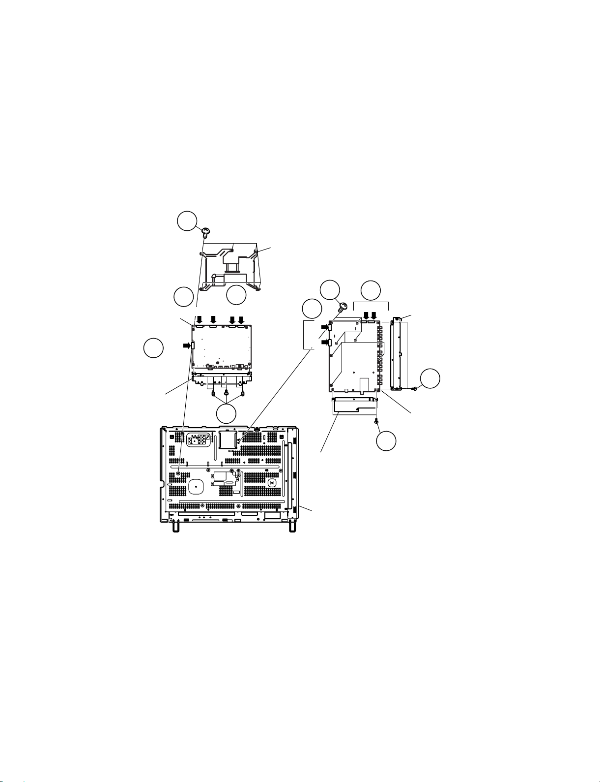
Page 37

2. REMOVING OF CHASSIS TRAY
1. Remove the 5 screws and detach the Chassis Tray.
3. REMOVING OF MINI-AV PWB
1. Disconnect the connecting cord.
2. Remove the 2 screws and detach the MINI-AV PWB Cover.
3. Detach the MINI-AV PWB.
4. Detach the MINI-AV PWB Holder.
5. Remove the 4 screws and detach the Side Chassis.
4. REMOVING OF KEY PWB
1. Remove the 3 screws and detach the Top Cover.
2. Remove the 2 screws and detach the Insulation Plate.
3. Disconnect the connecting cord.
4. Detach the KEY PWB.
5. Detach the Operate Button.
5. REMOVING OF SPEAKERS
1. Disconnect the connecting cord.
2. Detach the Speaker L/R and Sub woofer.
LC-65RX1M
㪦㫇㪼㫉㪸㫋㪼
㪙㫌㫋㫋㫆㫅
㪢㪜㪰㩷㪧㪮㪙
㪫㫆㫇㩷㪚㫆㫍㪼㫉
㪠㫅㫊㫌㫃㪸㫋㫀㫆㫅㩷㪧㫃㪸㫋㪼
4-1
䎾䎮䎰䏀
4-3
㪤㪠㪥㪠㪄㪘㪭㩷㪧㪮㪙㩷㪟㫆㫃㪻㪼㫉
2-1
㪚㪿㪸㫊㫊㫀㫊㩷㪫㫉㪸㫐
4-2
3-5
3-2
䎾䎫䎰䏀
3-1
䎾䎸䎶䏀
䎾䎹䎧䏀
3-2
㪤㪠㪥㪠㪄㪘㪭㩷㪧㪮㪙
㪤㪠㪥㪠㪄㪘㪭㩷㪧㪮㪙㩷㪚㫆㫍㪼㫉
㪪㫀㪻㪼
㪚㪿㪸㫊㫊㫀㫊
㪪㫇㪼㪸㫂㪼㫉
䎾䎶䎳䏀
4 – 3
5-1
䎾䎶䎳䏀
5-1
䎾䎶䎳䏀
5-1
㪪㫇㪼㪸㫂㪼㫉㪪㫌㪹㩷㪮㫆㫆㪽㪼㫉
Page 38

LC-65RX1M
6. REMOVING OF POWER PWB 1, POWER PWB 2 AND AC INLET PWB
1. Disconnect the connecting cord.
2. Remove the 6 screws and detach the POWER PWB 2.
3. Disconnect the connecting cord.
4. Remove the 6 screws and detach the POWER PWB 1.
5. Disconnect the connecting cord.
6. Remove the 6 screws and detach the AC INLET PWB.
7. REMOVING OF R/C, LED PWB
1. Remove the 1 screw and detach the CORNER F ANGLE (R BOTTOM).
2. Disconnect the connecting cord.
3. Remove the 2 screws and detach the R/C, LED PWB.
4. Detach the Irss Cover.
5. Detach the LED Cover.
6-2
㪠㫉㫊㫊㩷㪚㫆㫍㪼㫉
㪣㪜㪛㩷㪚㫆㫍㪼㫉
7-5
6-1
䎾䎳䎯䏀
䎾䎳䎨䏀
6-4
䎾䎳䎧䏀
䎾䎯䎤䎯䏀
6-3
䎾䎳䎳䎔䏀
䎾䎳䎳䎕䏀
6-6
㪘㪚㩷㪠㪥㪣㪜㪫㩷㪧㪮㪙
䎾䎳䎳䎔䏀
䎾䎳䎳䎕䏀
䎾䎯䎤䎵䏀
6-1
㪧㪦㪮㪜㪩㩷㪧㪮㪙㩷㪉
㪧㪦㪮㪜㪩
㪧㪮㪙㩷㪈
6-3
䎾䎤䎦䏀
䎾䎤䎦䏀
6-5
7-1
7-4
䎾䎵䎤䏀
7-2
7-3
㪩㪆㪚㪃㩷㪣㪜㪛㩷㪧㪮㪙
㪚㪦㪩㪥㪜㪩㩷㪝㩷㪘㪥㪞㪣㪜㩷㩿㪩㩷㪙㪦㪫㪫㪦㪤㪀
4 – 4
Page 39
8. REMOVING OF FRC PWB
1. Disconnect the connecting cord.
2. Remove the 4 screws and detach the FRC PWB.
䎾䎯䎤䎕䏀
8-1
8-1
8-1
LC-65RX1M
䎾䎯䎥䏀
䎾䎯䎤䎘䏀
8-1
䎾䎯䎺䏀
䎾䎩䎯䏀
䎾䎯䎩䏀
8-2
䎾䎶䎦䎙䎕䎔䎔䏀
䎾䎶䎦䎙䎕䎔䎕䏀
8-2
8-1
㪝㪩㪚㩷㪧㪮㪙
4 – 5
Page 40
LC-65RX1M
[3] REMOVING OF MAJOR PARTS FROM CHASSIS TRAY
1. REMOVING OF MAIN PWB
1. Remove the 6 screw and detach the MAIN PWB Shield.
2. Disconnect the connecting cord.
3. Detach the MAIN PWB.
4. Remove the 6 screws and detach the MAIN PWB Cover.
2. REMOVING OF SUB PWB
1. Disconnect the connecting cord.
2. Remove the 2 screws and detach the Terminal Cover Side.
3. Remove the 2 screws and detach the Tuner Cover.
4. Remove the 7 screws and detach the SUB PWB.
1-1
㪤㪘㪠㪥㩷㪪㪿㫀㪼㫃㪻
㪤㪘㪠㪥㩷㪧㪮㪙
1-2
㪤㪘㪠㪥㩷㪧㪮㪙
㪚㫆㫍㪼㫉
䎾䎵䎤䏀
1-2
䎾䎩䎵䏀
䎾䎯䎥䏀
䎾䎳䎧䏀
1-4
1-2
䎾䎸䎶䏀
2-4
2-1
䎾䎶䎳䏀
䎾䎳䎨䏀
㪫㫌㫅㪼㫉㩷㪚㫆㫍㪼㫉
㪚㪿㪸㫊㫊㫀㫊㩷㪫㫉㪸㫐
2-1
䎾䎹䎧䏀
䎾䎮䎰䏀
2-3
㪫㪼㫉㫄㫀㫅㪸㫃㩷
㪚㫆㫍㪼㫉㩷㪪㫀㪻㪼
2-2
㪪㪬㪙㩷㪧㪮㪙
4 – 6
Page 41

LC-65RX1M
LC65RX1M
CHAPTER 5. ADJUSTMENT PROCEDURE
ServiceManual
[1] ADJUSTMENT PROCEDURE
1. Adjustment method after PWB and/or IC replacement due to repair
The unit is set to the optimum at the time of shipment from the factory. If any value should become improper or any adjustment is necessary due to
the part replacement, make an adjustment according to the following procedure.
1. Procure the following units in order to replace the main unit, IC3301, IC8101, IC3501, IC3502, IC8301, IC8302, IC8303, or IC8304.
MAIN UNIT: DUNTKE630FM02
NOTE: [Caution when replacing ICs in the main unit (IC1501/IC1502/IC1503/IC2002) or the mini av unit (IC801)]
The above ICs are EEPROMs storing the EDID data of HDMI and the monitor microcomputer. Before replacing the relevant part, procure the
following parts in which the data have been rewritten.
IC2002 RH-IXB986WJNDQ Monitor microcomputer
IC801 RH-IXC284WJQZS INPUT4
IC1501 RH-IXC285WJQZS INPUT5
IC1502 RH-IXC286WJQZS INPUT6
IC1503 RH-IXC287WJQZS INPUT7
2. After replacing the LCD panel or LCD control PWB, check PANEL_SIZE in the following procedure.
1) Enter the process adjustment mode.
2) Use the cursor keys / and CH / of R/C to select the item [PANEL_SIZE] on the page 32/32.
3) Verify that the panel size is displayed.
4) If the size doesn't match, select the values of the panel size with the Vol +/- keys.
5) After selection in Step 4), press the ENTER key, and it is completed with OK displayed.
3. After replacing the LCD panel or LCD control PWB, adjust the VCOM in the following procedure.
1) Enter the process adjustment mode.
2) Use the cursor keys / and CH / of R/C to select the item [VCOM ADJ] on the page 9/32.
3) Press the ENTER key to verify that the adjustment pattern is displayed.
4) Use the +/- keys of VOL of L/C to adjust the flicker in the center of the screen to minimum.
5) When the optimal state is achieved in Step 4, press the ENTER key to turn the pattern to OFF.
5 – 1
Page 42

LC-65RX1M
(7)
(8)
2. Entering and exiting the adjustment process mode
1. Press the “POWER” key on the set of running TV set to force off the power.
2. While holding down the “VOL (-)” and “TV/VIDEO” keys on the set at once, press the “POWER” key on the set to turn on the power.
The letter “K” appears on the screen.
3. Next, hold down the “VOL (-)” and “CH ( )” keys on the set at once.
Multiple lines of character string appearing on the screen indicate that the set is now in the adjustment Process mode. If you fail to enter the
adjustment process mode (the display is the same as normal startup), retry the procedure. (Another procedure)
4. Press the “MENU” key on the main unit to display OSD.
5. Move the cursor to SERVICE (OSD) using the cursor keys on the remote control.
Then press the “MENU” key on the remote control to enter the service mode (adjustment process mode).
6. To exit the adjustment process mode after the adjustment is done, unplug the AC power cord to force off the power. (When the power is turned off
with the remote controller, once unplug the AC power cord and plug it in again. In this case, wait 10 seconds or so before plugging.)
CAUTION:Use due care in handling the information described here lest the users should know how to enter the adjustment process mode. If the
settings are tampered with in this mode, unrecoverable system damage may result.
3. Remote controller key operation and description of display in adjustment process mode.
1. key operation
Remote controller key Main unit key Function
CH (/)
CH ( / )
VOL (+/-) VOL (+/-) Changing a selected item setting (+1/-1)
Cursor ( / )
— Turning a page (PREVIOUS / NEXT)
Moving an item (line) by one (UP/DOWN)
Cursor ( / )
TV/VIDEO on remote
controller
— Changing a selected line setting (+10/-10)
— Input source switching (toggle switching) (TV→EXT1~8)
RETURN — Returning to a present page
ENTER — Executing a function
Input mode is switched automatically when relevant adjustment is started so far as the necessary input signal is available.
4. Description of display
(1) Page/ of present number of total pages (5) Inducing display
(2) Page present title (4) Present colour system (6) Model name
1/32 [INFO] INPUT1 AUTO ??? 42E_D83
MAIN Version
BOOT Version
Monitor Version
FRC Version
CPLD Version
EQ DATA CHECKSUM
LAMP ERROR
MONITOR ERR CAUSE
NORMAL STANDBY CAUSE
ERROR STANDBY CAUSE
(3) Input that has been selected now
1.00 (E 2007/07/10 D)
1.0
a6
ROM
0
11 11 11 11
0
1) 0 2) 0 3) 0
0H 0M 0H 0M 0H 0M
4) 0 5) 0
0H 0M 0H 0M
Item name
Parameter
No. Description Display specification
(1) Page/ of present number of total pages 2char/2char Decimal Number mark.
(2) Page present title It bundles it by Max. 15 char “[“ ”]”.
(3) Input that has been selected now TV/INPUT1/INPUT2/INPUT3/INPUT5/INPUT6/INPUT7/INPUT8
(4) Present colour system NTSC/PAL/SECAM/COMP15K/COMP33K/COMP45K/COMP28K/COMP31K
(5) Inducing display EUROPE/RUSSIA/SWEDEN
(6) Model name MODEL NAME
(7) Item name Max. 30 char
(8) Parameter Max. 60 char
5 – 2
Page 43

5. Adjustment process mode menu
The character string in brackets [ ] will appear as a page title in the adjustment process menu header.
Page Line Item Description Remarks (adjustment detail, etc.)
1/35 [INFO]
1 MAIN Version Main software version
2 BOOT Version BOOT Version.
3 Monitor Version Monitor software version
4 FRC Version FRC Version
5 CPLD Version CPLD Version.
6 EQ DATA CHECKSUM Audio data checksum.
7 LAMP ERROR Number of termination due to lamp error.
8 MONITOR ERR CAUSE Last error standby cause.
9 NORMALSTANDBY CAUSE Situation that became standby at the end.
(Excluding the error)
10 ERROR STANDBY CAUSE [1] 00H 00M Error standby cause Total operating time before error.
[2] 00H 00M
[3] 00H 00M
[4] 00H 00M
[5] 00H 00M
2/35 [INIT]
1 INDUSTRY INIT Enter Initialization to factory settings execution.
2 INDUSTRY INIT(-Hotel) OFF Initialization to factory settings execution.
(Hotel mode is excluded)
3 HOTEL MODE OFF Hotel mode setting execution.
4 Center Acutime 5H 0M Main operating hours.
5 RESET OFF Main operating hours reset.
6 Backlight Acutime 19H 35M Backlight operating hours.
7 RESET OFF Backlight operating hours reset.
8 LAMP ERROR RESET OFF Lamp error reset.
9 ADJ PARAM SET Enter ADJ PARAM SET
10 VIC XPOS 0 X-coordinate setting for VIC READ
11 VIC YPOS 0 Y-coordinate setting for VIC READ
12 VIC SIGNAL TYPE MAIN Signal type setting for VIC READ
13 VIC READ OFF Picture level acquisition function
(Level appears in green on the upper right)
3/35 [TUNER ADJ]
1 RF AGC ADJ Enter RF-AGC auto adjustment execution
2 TUNER ADJ Enter TUNER auto adjustment execution
3 PAL+TUNER ADJ Enter PAL TUNER auto adjustment execution
4 RF AGC ADJ(CA-8CH) Enter RF-AGC auto adjustment execution (CA-8CH)
5 TUNER ADJ(CA-8CH) Enter TUNER auto adjustment execution (CA-8CH)
6 PAL+TUNER ADJ(CA-8CH) Enter PAL TUNER auto adjustment execution (CA-8CH)
7 RF AGC 25 RF AGC adjustment
8 TUNER DAC 164 TUNER signal level adjustment
9RF AGC READ OFF
4/35 [PAL MAIN]
1 PAL ADJ Enter PAL adjustment
2 SECAM ADJ Enter SECAM adjustment
3 N358 ADJ Enter N358 adjustment
4 PAL CONTRAST 124 PAL contrast adjustment
5 SECAM CONTRAST 130 SECAM CONTRAST adjustment
6 N358 CONTRAST 121 N358 CONTRAST adjustment
5/35 [CEC TEST]
1 HDMI CEC TEST Enter CEC test
2 INSPECT USB TERM Enter
3 MONIDATA READ[TEMP/OPC] OFF MONITOR Temperature/ OPC Acquisition tool.
4 CAUSE RESET Enter
6/35 [COMP15KMAIN]
1 COMP15K ALL ADJ Enter Component 15K picture level adjustment
2 COMP15K MAIN Y GAIN 200 Y GAIN adjustment value
3 COMP15K MAIN CB GAIN 210 Cb GAIN adjustment value
4 COMP15K MAIN CR GAIN 209 Cr GAIN adjustment value
5 COMP15K Y OFFSET 65 Y OFFSET adjustment value
6 COMP15K CB OFFSET 512 Cb OFFSET adjustment value
7 COMP15K CR OFFSET 513 Cr OFFSET adjustment value
LC-65RX1M
5 – 3
Page 44

LC-65RX1M
Page Line Item Description Remarks (adjustment detail, etc.)
7/35 [HDTV]
1 HDTV ADJ Enter HDTV video level adjustment
2 HDTV Y GAIN 197 HDTV Y GAIN adjustment value
3 HDTV CB GAIN 211 HDTV Cb adjustment value
4 HDTV CR GAIN 208 HDTV Cr adjustment value
5 HDTV Y OFFSET 65 HDTV Y OFFSET adjustment value
6 HDTV CB OFFSET 513 HDTV Cb OFFSET adjustment value
7 HDTV CR OFFSET 513 HDTV Cr OFFSET adjustment value
8/35 [ANALOG PC]
1 ANALOG PC ADJ Enter DVI ANALOG video level adjustment
2 R OFFSET 64 R CUTOFF adjustment value
3 G OFFSET 63 G CUTOFF adjustment value
4 B OFFSET 64 B CUTOFF adjustment value
5 R GAIN 195 R DRIVE adjustment value
6 G GAIN 188 G DRIVE adjustment value
7 B GAIN 198 B DRIVE adjustment value
9/35 [LUMAADJ]
1VCOM ADJ 62
2 LCD LUMA ADJ Enter
3 LCD LUMA UP 0
4 LCD LUMA DOWN 0
10/35 [FR DDRTEST]
1 DDRA TEST1 Enter
2 DDRA TEST2 Enter
3 DDRB TEST1 Enter
4 DDRB TEST2 Enter
5 DDRB TEST3 Enter
6 FRC ON/OFF Enter
7 SOUSAM DDR BIST Enter
8 SOUSAS DDR BIST Enter
11/35 [LEV]
1 LEV1 176
2 LEV2 352
3 LEV3 528
4 LEV4 656
5 LEV5 800
6 LEV6 928
12/35 [MGXX1]
1 MG1R 185 W/B adjustment, gradation 1R adjustment value
2 MG1G 162 W/B adjustment, gradation 1G adjustment value
3 MG1B 141 W/B adjustment, gradation 1B adjustment value
4 MG2R 366 W/B adjustment, gradation 2R adjustment value
5 MG2G 324 W/B adjustment, gradation 2G adjustment value
6 MG2B 286 W/B adjustment, gradation 2B adjustment value
7 MG3R 544 W/B adjustment, gradation 3R adjustment value
8 MG3G 486 W/B adjustment, gradation 3G adjustment value
9 MG3B 443 W/B adjustment, gradation 3B adjustment value
13/35 [MGXX2]
1 MG4R 674 W/B adjustment, gradation 4R adjustment value
2 MG4G 604 W/B adjustment, gradation 4G adjustment value
3 MG4B 561 W/B adjustment, gradation 4B adjustment value
4 MG5R 812 W/B adjustment, gradation 5R adjustment value
5 MG5G 737 W/B adjustment, gradation 5G adjustment value
6 MG5B 700 W/B adjustment, gradation 5B adjustment value
7 MG6R 928 W/B adjustment, gradation 6R adjustment value
8 MG6G 855 W/B adjustment, gradation 6G adjustment value
9 MG6B 843 W/B adjustment, gradation 6B adjustment value
5 – 4
Page 45

Page Line Item Description Remarks (adjustment detail, etc.)
14/35 [G CO POS]
1 MODE SELECT FACTORY
2 POS SELECT WB IN
3POS MIN 0
4 POS MID1 176
5 POS MID2 352
6 POS MID3 528
7 POS MID4 656
8 POS MID5 800
9 POS MID6 928
10 POS MAX 1023
15/35 [G CO CD]
1 CD MIN 0
2 CD MID1 0
3 CD MID2 0
4 CD MID3 0
5 CD MID4 0
6 CD MID5 0
7 CD MID6 0
8 CD MAX 0
16/35 [G CO VOL]
1CALC OFF
2 RESET OFF
3 VAL1 100
4 VAL2 100
5 VAL3 100
6 VAL4 100
7 VAL5 100
8 VAL6 100
17/35 [ACTIVEBL1]
1 ABL TEST MODE Enter
2 PRINT DEBUG OFF
18/35 [SOUND1]
1 AUDIO_PARAMETER_SWITCH ROM
2AU_FLAT
3 INPUT_MIXER_GAIN
4 OUTPUT_MIXER_GAIN
5 PEQ1_F0
6 PEQ1_Q
7 PEQ1_GAIN
8 PEQ2_F0
9 PEQ2_Q
10 PEQ2_GAIN
11 PEQ3_F0
12 PEQ3_Q
13 PEQ3_GAIN
19/35 [SOUND 2]
1 PEQ4_F0
2 PEQ4_Q
3 PEQ4_GAIN
4 PEQ5_F0
5 PEQ5_Q
6 PEQ5_GAIN
7 GAIN_ADJUSTER1
8 GAIN_ADJUSTER2
9 GAIN_ADJUSTER3
10 GAIN_ADJUSTER4
11 GAIN_ADJUSTER5
12 GAIN_ADJUSTER6_SP
13 GAIN_ADJUSTER6_HP
LC-65RX1M
5 – 5
Page 46

LC-65RX1M
Page Line Item Description Remarks (adjustment detail, etc.)
20/35 [SOUND 3]
1 LOUT1_VOLUME_CONTROL
2 ROUT1_VOLUME_CONTROL
21/35 [M PWM]
1PWM
2PWM FREQ
3 PWM DUTY
4OSC FREQ
5 OSC DUTY
22/35 [M OPC1]
1 OPC LDUTY0
2 OPC LDUTY1
3 OPC LDUTY2
4 OPC LDUTY3
5 OPC LDUTY4
6 OPC LDUTY5
7 OPC LDUTY6
8 OPC LDUTY7
9 OPC LDUTY8
10 OPC LDUTY9
11 OPC LDUTY10
12 OPC LDUTY11
23/35 [M OPC2]
1 OPC LDUTY12
2 OPC LDUTY13
3 OPC LDUTY14
4 OPC LDUTY15
5 OPC LDUTY16
6 OPC LDUTY17
7 OPC LDUTY18
8 OPC LDUTY19
9 OPC LDUTY20
10 OPC LDUTY21
11 OPC LDUTY22
24/35 [M OPC3]
1 OPC LDUTY23
2 OPC LDUTY24
3 OPC LDUTY25
4 OPC LDUTY26
5 OPC LDUTY27
6 OPC LDUTY28
7 OPC LDUTY29
8 OPC LDUTY30
9 OPC LDUTY31
10 OPC LDUTY32
25/35 [M ADL1]
1 OPC33 ADLEVEL 0
2 OPC33 ADLEVEL 1
3 OPC33 ADLEVEL 2
4 OPC33 ADLEVEL 3
5 OPC33 ADLEVEL 4
6 OPC33 ADLEVEL 5
7 OPC33 ADLEVEL 6
8 OPC33 ADLEVEL 7
9 OPC33 ADLEVEL 8
10 OPC33 ADLEVEL 9
11 OPC33 ADLEVEL 10
12 OPC33 ADLEVEL 11
5 – 6
Page 47

Page Line Item Description Remarks (adjustment detail, etc.)
26/35 [M ADL2]
1 OPC33 ADLEVEL 12
2 OPC33 ADLEVEL 13
3 OPC33 ADLEVEL 14
4 OPC33 ADLEVEL 15
5 OPC33 ADLEVEL 16
6 OPC33 ADLEVEL 17
7 OPC33 ADLEVEL 18
8 OPC33 ADLEVEL 19
9 OPC33 ADLEVEL 20
10 OPC33 ADLEVEL 21
11 OPC33 ADLEVEL 22
27/35 [M ADL3]
1 OPC33 ADLEVEL 23
2 OPC33 ADLEVEL 24
3 OPC33 ADLEVEL 25
4 OPC33 ADLEVEL 26
5 OPC33 ADLEVEL 27
6 OPC33 ADLEVEL 28
7 OPC33 ADLEVEL 29
8 OPC33 ADLEVEL 30
9 OPC33 ADLEVEL 31
28/35 [M V6THE]
1V6 OS THERMO 1 72
2V6 OS THERMO 2 86
3V6 OS THERMO 3 96
4 V6 OS THERMO 4 108
5 V6 OS THERMO 5 120
6 V6 OS THERMO 6 132
7 V6 OS THERMO 7 144
29/35 [M V5THE]
1V5 OS THERMO 1 72
2V5 OS THERMO 2 86
3V5 OS THERMO 3 96
4 V5 OS THERMO 4 108
5 V5 OS THERMO 5 120
6 V5 OS THERMO 6 132
7 V5 OS THERMO 7 144
30/35 [M BLCTL TEMP]
1BL TEMP1
2BL TEMP2
3BL TDUTY
31/35 [M EEP SET]
1 MONITOR TIME OUT ON Monitor and the main communication time-out setting
2 MONITOR MAX TEMP 43 MONITOR MAX temperature setting
3 MONITOR EEP READ / WRITE WRITE MONITOR EEPROM READ/WRITE Setting/execution
4 MONITOR EEP ADR 0x 0 MONITOR EEPROM arbitrary addressing
5 MONITOR EEP DATA 0x 0 MONITOR EEPROM arbitrary data specification
32/35 [M TEST PATTERN]
1 LCD TEST PATTERN OFF Pattern with built-in LCD controller display
33/35 [MEM CLEAR]
1 KEY LOCK(1217) Enter
2 KOUTEI AREA ALL CLEAR Adjustment value clearness in all areas in process
3 A MODE AREA CLEAR Adjustment value clearness of process A mode
4 BACKUP AREA CLEAR Adjustment value clearness in process backup area
5 B MODE AREA CLEAR Adjustment value clearness of process B mode
6 EXECUTION Clear execution
LC-65RX1M
5 – 7
Page 48
LC-65RX1M
Page Line Item Description Remarks (adjustment detail, etc.)
34/35 [FR REGI]
1 READ/WRITE READ
2 SLAVE ADDRESS SLAVE0
3 REGISTOR ADDRESS 0x 0
0x 0
4 WRITE DATA 0x 0
0x 0
5 READ DATA 0x 0
0x 0
35/35 [ETC]
1 EEP SAVE OFF Writing setting values to EEPROM.
2 EEP RECOVER OFF Reading setting values from EEPROM.
3 MONITOR ERROR CAUSE RESET OFF
4 STANDBY CAUSE RESET OFF Reset stand by cause.
5 MODEL NAME RX1 Model name setting
6 PANEL SIZE 65 Panel size setting.
7 PRODUCT EEP ADR 0x 0
8 PRODUCT EEP DATA 0x 0
5 – 8
Page 49

LC-65RX1M
6. Special features
1. NORMAL STANDBY CAUSE (Page 1/32)
Display of a cause (code) of the last standby.
The cause of the last standby is recorded in EEPROM whenever possible.
Checking this code will be useful in finding a problem when you repair the troubled set.
2. EEP SAVE (Page 32/32)
Storage of EEP adjustment value
3. EEP RECOVER (Page 32/32)
Retrieval of EEP adjustment value from storage area.
7. Lamp error detection
1. Function
This LCD color TV set incorporates a lamp error detection feature that automatically turns off the power for safety under abnormal lamp or lamp
circuit conditions. If by any chance anything is wrong with the lamp or lamp circuit or if the lamp error detection feature is activated for some reason, the following will result.
1) The power is interrupted in about 6 seconds after it is turned on.
(The power LED on the front of the TV set turns red from green and keeps blinking in red: ON for 250 ms and OFF for 1 sec.).
2) If the above phenomenon 1) occurs 5 times consecutively, it becomes impossible to turn on the power. (The power LED remained red).
2. Measures
1) Checking with lamp error detection OFF
Enter the adjustment process mode, referring to 1. Entering and exiting the adjustment process mode.
If there is a problem with the lamp or lamp circuit, the lamp will go out. (The power LED is green.)
Then, you can check the operation to see if the lamp and lamp circuit are in trouble.
2) Resetting the lamp error count
After the lamp and lamp circuit are found out of trouble, reset the lamp error count. If a lamp error is detected five consecutive times, the power
cannot be turned on. Using the cursor (UP/DOWN) key, move to the cursor to [LAMP ERROR RESET], Line 8 on adjustment process mode
service page 2/33. With the cursor (LEFT/RIGHT) keys, select the [LAMP ERROR RESET] value. Finally press the cursor (ENTER) eys to
reset the value to “0”.
Table of contents of adjustment process mode Page 2/32
[INIT]
INDUSTRY INIT Enter
INDUSTRY INIT(-Hotel) OFF
HOTEL MODE OFF
Center Acutime
RESET
Backlight Acutime
RESET
LAMP ERROR RESET
ADJ PARAM SET Enter
VIC XPOS 0
VIC YPOS 0
VIC SIGNAL TYPE MAIN
VIC READ OFF
OFF
OFF
OFF
Resetting to "0"
5 – 9
Page 50

LC-65RX1M
8. STANDBY CAUSE FUNCTIONS
This model is equipped with a STANDBY CAUSE FUNCTIONS which stores the cause of why the unit is turned off and displays it on adjustment process mode.
1. NORMAL STANDBY CAUSE
ERROR CODE here indicates cause of standby in normal operation or Function of the Unit.
No display when the unit is turned off with R/C.
Only the latest cause is indicated.
2. ERROR STANDBY CAUSE
ERROR CODE here indicates cause of Error in the unit.
It also indicates accumulated operating times of the unit.
The last five histories are displayed.
1)-5) five histories 1) is the latest.
When there is no error, error code is ‘0’ and no characters appear.
3. MONITOR ERROR CAUSE
When the monitor micom detects an error, ERROR CODE is displayed.
The number of flashing Power LED and OPC LED indicates location of error detected.
This number stores the latest four contents of the error. ‘0’ is displayed when no error.
• NORMAL STANDBY CAUSE
Display Code Indication Description
2 NO_OPERT in the cause of “no operation off”
3 NO_SIGNA in the cause of “no signal off”
6 SLEEP_TM in the cause of “SLEEP timer”
8 OFF_232C in the cause of command by RS-232C
• ERROR STANDBY CAUSE
Display Code Indication Description
17 E_AVCTMP in the cause of abnormal temperature
• MONITOR ERROR CAUSE
Display Error Reason
01 Initial Communication Error 1 Not used
02 Initial Communication Error 2 Cannot receive initial communication from main CPU 3 times 1 time
03 Initial Communication Error 3 Receive initial communication only 3 times 2 times
04 Initial Communication Error 4 To the communication setting reception 3 times 2 times
05 Initial Communication Error 5 To the initialization completion reception 3 times 2 times
06 Initial Communication Error 6 To the notice of version reception 3 times 2 times
07 Initial Communication Error 7 To the notice of start information reception 3 times 2 times
08 Initial Communication Error 8 To the start information answer reception 3 times 2 times
09 Initial Communication Error 9 To the time-out setting reception 3 times 2 times
0A Communication Error A Request Time-out 3 times Off
0B Communication Error B Restart Time-out 3 times 4 times
0C Communication Error C End sequence Time-out Off Off
0D Communication Error D Reserve start Time-out when End seqence Off Off
0E Communication Error E Download Start Time-out 3 times Off
0F Communication Error F Get Time Start Time-out Off Off
10 Communication Error G Not used
11 Communication Error H Watchdog Time-out 3 times 3 times
12 Communication Error I Not used
13 Communication Error J Not used
14 Communication Error K Not used
15 Power (RED) LED Blink 0 Not used
16 Power (RED) LED Blink 1 Lamp Error 1 time Off
17 Power (RED) LED Blink 2 AC_DET Error 2 times 1 time
18 Power (RED) LED Blink 3 Not used
19 Power (RED) LED Blink 4 Not used
1A Power (RED) LED Blink 5 Monitor Temperature Error 5 times Off
1B Power (RED) LED Blink 6 Not used
1C Power (RED) LED Blink 7 Not used
1D Power supply Error 1 PS_ON(DET_10V) Error 2 times 3 times
1E Power supply Error 2 Not used
Power (RED) LED
Blink Times
OPC LED
Blink Times
5 – 10
Page 51

LC-65RX1M
Display Error Reason
1F Power supply Error 3 Not used
20 Power supply Error 4 D_POW(DET_D3V3) Error 2 times 4 times
21 Power supply Error 5 Panel Power Error 2 times 5 times
22 Power supply Error 6 Not used
23 Main micom Error Error Standby request from Main CPU 2 times 7 times
24 Power supply Error 7 AC_DET Error (during power on sequence) 2 times 1 time
Power (RED) LED
Blink Times
OPC LED
Blink Times
5 – 11
Page 52
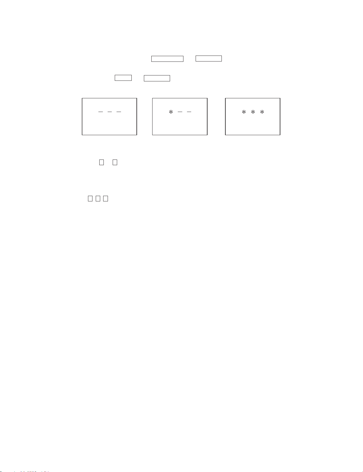
LC-65RX1M
9. Public Mode (Hotel Mode)
1. Starting the Public Mode
• There are two following ways to display the PUBLIC Mode setting screen.
1) On the process adjustment mode screen (2/32), set the “HOTEL MODE” Flag to ON.
Turn off the power, and turn it on again, pressing the and keys of the main unit at the same time.
CHANNEL UP
Volume UP
2) Enter the Pass Word, and start the unit.
a) Turn on the power, pressing the and keys of the main unit at the same time.
INPUT
Volume UP
b) Display the Pass Word input screen.
Operation procedure
• The initial input position is the digit at the left end.
9
• For the numeric keys to of R/C, key input is accepted. Input of the other keys is prohibited.
0
• Change “-” to “*” by inputting the numeric key at the input position, and shift the input position rightward one digit.
• When three digits are completely input, the Pass Word is judged.
c) Check the Pass Word by inputting three digits.
2 7
If the Pass Word is , it shifts to the PUBLIC Mode setting screen.
0
In another case, the screen is erased, and it operates in the ordinary mode.
2. Exiting the Public Mode screen
• There are two following ways to exit the Public Mode setting screen.
1) Turn off the power.
2) Select “Execution” in the PUBLIC_Mode to execute it.
Activate the restart under the set content. Here, the START input SOURCE setting is excluded since this item is referred to only when the
power is turned on.
3. Set value of the Public Mode
• Each set value in the PUBLIC Mode is initialized when the factory setting is applied.
(The setting of the PUBLIC MODE Flag in the process adjustment mode screen is not changed.)
5 – 12
Page 53

4. Basic operation in the Public Mode
Volume +/- or Cursor /
Channel / or Cur-
sor /
Decision (ENTER) Execution (Used by the items “Execution” and “RESET”.)
PUBLIC Mode R/C Ordinary operation mode: It enters the PUBLIC Mode.
PUBLIC Mode: It exits the PUBLIC Mode.
Change or execution of the set value.
Movement to the selected item.
PUBLIC MODE Flag is set to “ON”.
PUBLIC MODE Flag does not change.
Any set item in PUBLIC Mode is not initialized.
Public Mode
POWER ON FIXED [VARIABLE]
SHUT DOWN MODE [NORMAL]
MAXIMUM VOLUME [60]
VOLUME FIXED [VARIABLE]
VOLUME FIXED LEVEL [20]
RC BUTTON [RESPOND]
LC-65RX1M
PANEL BUTTON [RESPOND]
MENU BUTTON [RESPOND]
AV POSITION FIXED [VARIABLE]
ON SCREEN DISPLAY [YES]
INPUT MODE START [NORMAL]
INPUT MODE FIXED [VARIABLE]
LOUD SPEAKER [ON]
RC PATH THROUGH [OFF]
232C POWON [DISABLE]
HOTELMODE [ON]
RESET
EXECUTE
5. Operation after “RESET”
Select “RESET” in the PUBLIC Mode, and it operates as follows when it is executed (refer to the basic operation).
• The set contents in the PUBLIC mode are initialized.
• It does not exit the PUBLIC mode.
• PUBLIC MODE Flag does not change. (It is not set to OFF.)
5 – 13
Page 54

LC-65RX1M
6. Setting items (* Item names and selective items are expressed in English.)
1) Power ON Fixed (POWER ON FIXED)
Selection “VARIABLE” or “FIXED” is selectable. (Loop is provided.)
Default “VARIABLE”
Function • When "FIXED" is set, “Power ON/Standby Key” of the main unit and R/C is disabled.
Keys disabled when not
set to Default
Remarks The function does not work for any other standby factors (see below).
If the power button is pressed in the ordinary mode when set to “FIXED”, the caution is displayed for 5 seconds.
When power button on the main unit is pressed When power button on R/C is pressed
* The OSD display is an example.
If another ODS is previously displayed, the status is reset (MENU or similar).
2) Volume Maximum Level [MAXIMUM VOLUME]
Selection 0~60 (Loop is not provided.)
Default 60
Function • Even if VOL is adjusted to a value higher than the adjusted one, it is not set to that value. (Only the speakers of
Exception
Remarks • When it is set to 59 or less, the number is displayed and the volume bar is not displayed during operation in the
• OFF_TIMER (SLEEP)
• No operation OFF
• No signal OFF (including the power management)
No Power off by power button. No Power off by remote control.
the main unit)
ordinary mode.
• VOLUME can be abbreviated to VOL.
3) Volume Fixed [VOLUME FIXED]
Selection “VARIABLE” or “FIXED” is selectable. (Loop is provided.)
Default “VARIABLE”
Function It is selectable whether or not the volume is fixed to the value adjusted in the volume fixed level mode. (Only the
speakers of the main unit)
Exception • In the adjustment process, the volume can be set as desired regardless of this setting.
Keys disabled when not
set to Default
Remarks • Volume Fixed is prior to Volume Maximum Level.
4) Volume Fixed Level [VOLUME FIXED LEVEL]
Selection 0~60 (Loop is not provided.)
Default Currently set volume
Function The volume is fixed to the adjusted value. (Only the speakers of the main unit)
Exception • In the adjustment process, the volume can be set as desired regardless of this setting.
Keys disabled when not
set to Default
Remarks • When Volume Fixed is set to “VARIABLE”, the setting is inhibited to change.
• Volume high/low (VOL+/-) (Both R/C and main unit)
• Mute (MUTE)
• Even if the above disabled keys are operated, the volume is not displayed.
• VOLUME can be abbreviated to VOL.
• VOLUME can be abbreviated to VOL.
5 – 14
Page 55
LC-65RX1M
5) R/C Operation [RC BUTTON]
Selection “RESP0ND” or “NO RESPOND” is selectable. (Loop is provided.)
Default RESP0ND
Function R/C key operation is set.
Exception • Regardless of the setting contents, the process mode, inspection mode and PUBLIC_Mode Key are enabled.
Remarks The CARD function stops all functions including the input switching and direct key when set to “NO RESPOND”.
6) Main Unit Operation [PANEL BUTTON]
Selection “RESP0ND” or “NO RESPOND” is selectable. (Loop is provided.)
Default RESP0ND
Function NO RESPOND: Excluding power supply (Video/Standby key), the main unit keys are disabled.
Exception • Regardless of the setting contents, the start operation of the process mode, inspection mode and PUBLIC_Mode
7) MENU Operation [MENU BUTTON]
Selection “RESP0ND” or “NO RESPOND” is selectable. (Loop is provided.)
Default RESP0ND
Function The MENU keys on the main unit and R /C MENU are disabled.
Exception • Regardless of the setting contents, the start operation of the process mode, inspection mode and PUBLIC_Mode
Key that becomes
invalid excluding Default
besides MENU Key
because of setting
Remarks When set to “NO RESPOND”,
When set to “NO RESPOND”, the R/C keys are disabled in the ordinary mode.
The power key (Power ON/Standby Key) is also disabled.
• Regardless of the setting contents, all keys can be used while entering the process mode, inspection mode or
PUBLIC_Mode.
is enabled.
• Regardless of the setting contents, all keys can be used while entering the process mode, inspection mode and
PUBLIC_Mode.
is enabled.
• Regardless of the setting contents, all keys can be used whileentering the process mode, inspection mode or
PUBLIC_Mode.
ON_TIMER, Auto Preset, Manual_Memory, and clock setting
All Direct Shift keys to the MENU display
• ON_TIMER is set to “OFF”.
8) ODS Display [ON SCREEN DISPLAY]
Selection “YES” or “NO” is selectable. (Loop is provided.)
Default YES
Function When set to “ON”, the following OSD is not displayed.
Register, Setting, Adjustment MENU, Channel_Call, Volume Bar
In the case of Wide Model, if the following operation is performed, it is immediately switched (since MENU can not be
displayed).
Input switching
Keys which can be
enabled (Exquisite
example)
Keys disabled when not
set to Default (Example)
Remarks • When set to “ON”,
9) Start Mode [INPUT MODE START]
Selection “NORMAL”, “TV(*Channel)”, “INPUT1”, “INPUT2” (Loop is provided.)
Default NORMAL
Function When the power is ON, the input source or channel to start is set.
Remarks • When set to a mode other than “NORMAL”,
Brightness sensor, light control
Still screen, screen display, MENU, OFF_TIMER, A V Position, Wide Mode switch, Auto Instolation
a) The OFF_TIMER (SLEEP TIMER) setting time is cleared.
In the NORMAL mode, it follows the contents of Last_Memory.
a) It is inhibited to display the Channel Setting MENU and to set the Channel.
b) On start with “ON_TIMER”, the set Channel of ON_TIMER is prior.
• When set to “NORMAL”, “Mode Fixed (START MODE FIXED)” is set to “VARIABLE” to inhibit the selection.
5 – 15
Page 56

LC-65RX1M
10)Mode Fixed [INPUT MODE FIXED]
Selection “VARIABLE” or “FIXED” is selectable. (Loop is provided.)
Default VARIABLE
Function When set to “FIXED”, it is disable to switch to other channel or input after start in the set value of “Start Mode (INPUT
Keys disabled when not
set to Default (Example)
Remarks • When “START MODE” is set to “NORMAL”, this item is disable to set. (Automatically set to “VARIABLE”.)
MODE START)”.
Channel UP/Down, Direct, Channel Button, FLASHBACK, INPUT, STILL, Digit Select and Direct input switching
• When set to “FIXED”,
The Channel setting MENU (Menu-setup-Auto Installation, Programme setup and Child Lock item hatching) and
Input Selection MENU in MENU are not displayed.
10. Video signal adjustment procedure
* The adjustment process mode menu is listed in Section 4.
Signal generator level adjustment check (Adjustment to the specified level)
• Composite signal PAL : 0.7Vp-p ± 0.02Vp-p (Pedestal to white level)
• RGB signal : 0.7Vp-p ± 0.02Vp-p
• 15K component signal (50 Hz) : Y level : 0.7Vp-p ± 0.02Vp-p (Pedestal to white level)
: PB, PR level : 0.7Vp-p ± 0.02Vp-p
1. Entering the adjustment process mode
Enter the adjustment process mode according to Section 3.
2. RF AGC adjustment
Adjustment point Adjustment Conditions Adjustment procedure
1 Setting [Signal]
PAL
Split Field Colour Bar RF signal
U/V
• Feed the PAL Split Field colour bar signal (E-12ch) to TUNER.
Signal level: 55 dB µV ± 1dB (75Ω LOAD)
[E-12CH]
[Terminal]
TUNER
2 Auto adjustment
performance
3. PAL signal & tuner adjustment
Adjustment point Adjustment Conditions Adjustment procedure
1 Setting [Signal]
Page 3/32 Bring the cursor on [RF AGC ADJ] and press [ENTER] [RF AGC ADJ OK]
PAL
Full Field Color Bar Composite
or RF signal
[Terminal]
INPUT1 VIDEO INPUT
TUNER
㸡100% white
appears when finished.
• Feed the PAL full field colour bar signal (75% colour saturation) to INPUT1
VIDEO INPUT.
• Feed the RF signal (PAL colour bar) to TUNER.
• Make sure the PAL colour bar pattern has the sync level of 7:3 with the picture level.
㪲VIDEO IN SIGNAL]
㸡100% white
[RF Signal]
㸡100% white
5 – 16
Page 57

Adjustment point Adjustment Conditions Adjustment procedure
2 Auto adjustment
performance
4. SECAM adjustment
Adjustment point Adjustment Conditions Adjustment procedure
1 Setting [Signal]
Page 3/32 Bring the cursor on [PAL+TUNER ADJ] and press [ENTER] [PAL+TUNER ADJ
SECAM
Full Field Colour Bar signal
[Terminal]
INPUT1 VIDEO IN
LC-65RX1M
OK] appears when finished.
• Feed the SECAM full field colour bar signal (75% colour saturation) to
INPUT1 VIDEO INPUT.
2 Auto adjustment
performance
5. N358 adjustment
Adjustment point Adjustment Conditions Adjustment procedure
1 Setting [Signal]
2 Auto adjustment
performance
6. ADC adjustment (Component 15K)
Adjustment point Adjustment Conditions Adjustment procedure
1 Setting [Signal]
Page 4/32 Bring the cursor on [SECAM ADJ] and press [ENTER] [SECAM ADJ OK]
N358
Full Field Colour Bar signal
[Terminal]
INPUT1 VIDEO IN
Page 4/32 Bring the cursor on [N358 ADJ] and press [ENTER] [N358 ADJ OK] appears
COMP15K, 50Hz (576i)
100% Full Field Colour Bar signal
100% white
appears when finished.
• Feed the N358 full field colour bar signal (75% colour saturation) to INPUT1
VIDEO INPUT.
100% white
when finished.
• Feed the COMPONENT 15K (576i) 100% full field colour bar signal (100%
colour saturation) to INPUT1 COMPONENT INPUT.
Black
Black
2 Auto adjustment
performance
[Terminal]
INPUT1 COMPONENT INPUT
100% white
Page 6/32 Bring the cursor on [COMP15k ALL ADJ] and press [ENTER] [COMP15k ALL
ADJ OK] appears when finished.
Black
5 – 17
Page 58

LC-65RX1M
7. ADC adjustment (Component 33K)
Adjustment point Adjustment Conditions Adjustment procedure
1 Setting [Signal]
COMP33K, 50Hz (1080i)
100% Full Field Colour Bar signal
[Terminal]
INPUT1 COMPONENT INPUT
• Feed the COMPONENT 33K 100% (1080i) full field colour bar signal (100%
colour saturation) to INPUT1 COMPONENT INPUT.
Black
Black
2 Auto adjustment
performance
8. DVI-I adjustment (ANALOG D-sub15PIN)
Adjustment point Adjustment Conditions Adjustment procedure
1 Setting [Signal]
2 Auto adjustment
performance
Page 7/32 Bring the cursor on [HDTV ADJ] and press [ENTER] [HDTV ADJ OK] appears
XGA 60Hz
100% Full Field Colour Bar signal
[Terminal]
INPUT7 PC IN
Page 8/32 Bring the cursor on [DVI ANALOG PC ADJ] and press [ENTER] [DVI ANALOG
100% white
when finished.
• Feed the XGA 60Hz 100% full field colour bar signal (100% colour saturation) to INPUT7 PC IN.
100% white
PC ADJ OK] appears when finished.
11. White Balance Adjustment
Adjustment gradation values (IN) appear on page 11/32 of process adjustment, and adjustment initial values (offset value) appear on pages 12/32
and 13/32.
For white balance adjustment, adjust the offset values on pages 12/32 and 13/32.
[Condition of the unit for inspection]: Modulated light: MAX (+16)
[Adjustment reference device] : Minolta CA-210
[Adjustment]
Check that the values on page 11/32 of process adjustment are set as below. If not, change them accordingly.
Point 1 (LEV1) 176
Point 2 (LEV2) 352
Point 3 (LEV3) 528
Point 4 (LEV4) 656
Point 5 (LEV5) 800
Point 6 (LEV6) 928
1) Display the current adjustment status at point 6. (Page 11/32 of process adjustment)
The display for checking the adjustment status is toggled by pressing the “6” button on the remote control.
(Normal OSD display → “6” → display for check (OSD disappears) → “6” → normal OSD display → . . . )
2) Read the value of the luminance meter. x=0.272, y =0.277
3) Change MG6R/MG6B (Adjustment offset value) on page 13/32 of process adjustment so that the values of the luminance meter approach x=0.272
and y =0.277.
(Basically, G is not changed. If adjustment fails with R and B, change G. When G is lowered, the weaker of R and B must be fixed.)
4) Display the adjustment status of the current point 5. (Each time the “5” button on the remote control is pressed, the adjustment status check display is toggled.)
(Normal OSD display → “5” → Check display (OSD disappears) → “5” → Normal OSD display → . . . )
Change MG5R/MG5B (adjustment offset value) on page 13/32 of process adjustment so that the values of the luminance meter approach x =
0.272 and y = 0.277.
5 – 18
Page 59

LC-65RX1M
5) Repeat step 4) for points 4, 3, 2, and 1.
[Adjustment reference standard value]
Adjustment spec ± 0.002 Inspection spec ± 0.004 (point 1 and 2)
Adjustment spec ± 0.001 Inspection spec ± 0.002 (Excluding the above-mentioned)
* Adjusting procedure by use of [RS-232C]
1. Get ready the PC with COM port (RS-232C) running on Windows 95/98/ME/2000/XP operating system, as well as the RS-232C cross cable.
2. Start the unit with the RS-232C cable connected.
3. Start the terminal software. (The freeware readily available on the Internet will do.)
4. Make the following settings.
Baud rate 9,600 bps
Data LENGTH 8 bit
Parity bit None
Stop bit 1 bit
Flow control None
5. If the settings are correct, the terminal software indicates “ERR” against pressing of the “ENTER” key.
6. After the settings are done correctly, it is possible to make an adjustment by typing in the command shown in the table below and pressing the
“ENTER” key on the keyboard.
7. Command entry is successful if the terminal software indicates “OK” when the “ENTER” is pressed. If “ERR” is shown, retry to enter the command.
8. Send the process mode switching command to switch from the RS232C operation mode to the process mode.
KRSW0001: “ERR” is returned.
KKT10037: When “OK” is returned, the process mode becomes active. When “ERR”, start over from KRSW0001.
9. Send each adjustment command.
RS-232C command list
Command Function Remarks
KYOF0000 Remote control disabled
OSDS0001 OSD display inhibited
SBSL0016 Light control level MAX
MSET0001 Background adjustment start
MSET0004 Initialization of adjustment value
LEV60928 Graduation 6 (928-graduation adjustment)
MG6G **** Adjustment of G of graduation 6 0000 ~ 4095
MG6R **** Adjustment of R of graduation 6 0000 ~ 4095
MG6B **** Adjustment of B of graduation 6 0000 ~ 4095
LEV50800 Graduation 5 (800-graduation adjustment)
MG5G **** Adjustment of G of graduation 5 Calculated value
MG5R **** Adjustment of R of graduation 5 0000 ~ 4095
MG5B **** Adjustment of B of graduation 5 0000 ~ 4095
LEV40656 Graduation 4 (656-graduation adjustment)
MG4G **** Adjustment of G of graduation 4 Calculated value
MG4R **** Adjustment of R of graduation 4 0000 ~ 4095
MG4B **** Adjustment of B of graduation 4 0000 ~ 4095
LEV30528 Graduation 3 (528-graduation adjustment)
MG3G **** Adjustment of G of graduation 3 Calculated value
MG3R **** Adjustment of R of graduation 3 0000 ~ 4095
MG3B **** Adjustment of B of graduation 3 0000 ~ 4095
LEV20352 Graduation 2 (352-graduation adjustment)
MG2G **** Adjustment of G of graduation 2 Calculated value
MG2R **** Adjustment of R of graduation 2 0000 ~ 4095
MG2B **** Adjustment of B of graduation 2 0000 ~ 4095
LEV10184 Graduation 1 (176-graduation adjustment)
MG1G **** Adjustment of G of graduation 1 Calculated value
MG1R **** Adjustment of R of graduation 1 0000 ~ 4095
MG1B **** Adjustment of B of graduation 1 0000 ~ 4095
MSET0003 Writing of adjustment value
5 – 19
Page 60

LC-65RX1M
30%
0%
12. Confirmation item
1. Magi-Link Inspection
The thing that the Magi-Link circuit operates is confirmed.
2. HDMI-CEC Inspection
The thing that the HDMI-CEC circuit operates is confirmed.
13. Initialization to factory settings
CAUTION:When the factory settings have been made, all user setting data, including the channel settings, are initialized.
1 Factory settings ends by turning off the
After adjustments, exit the adjustment process mode.
To exit the adjustment process mode, turn off the MAIN power key.
When the power is turned off with the remote control, unplug the AC power cord and plug it back in.
(The adjustments done in the adjustment process mode are not initialized.) Keep this in mind when initializing these settings.
Adjustment item Adjustment conditions Adjustment procedure
[Factory setting with adjustment process mode]
MAIN POWER key.
(See to below caution)
• Enter the adjustment process mode.
• Move the cursor to [INDUSTRY INIT] on page 2/32.
• “EXECUTING” display appears.
• After a while, “SUCCESS” display appears, the setting is completed.
When succeeding: Background color (green)
When failing: Background color (red)
The following items are initialized in the factory setting.
1) User settings
2) Channel data (e.g. broadcast frequencies)
3) Maker option setting
4) Password data
14. Upgrading the software
1. Turn off the AC power (Unplug the AC power cord).
2. Insert the upgrading USB flash memory for upgrade into the service slot.
3. While holding down the power button, plug in the AC power cord of the main unit to turn on the power.
4. Upgrade begins automatically.
After the set starts, the upgrade screen like the figure below is displayed.
<SYSTEM UPGRADE>
System Version: E0708021
BANK 1
BANK 2
STATUS
UPDATING. . .
5. If any of the procedures fails, the following upgrade failure screen shows up. For the failing procedure, the “NG” marking turns red.
NOTE: In such case, try to upgrade the software again. If it still fails, the hardware may be in trouble.
5 – 20
Page 61

LC-65RX1M
100%
44%
100%
100%
<SYSTEM UPGRADE>
System Version: E0708021
BANK 1
OK
BANK 2
STATUS
UPDATING. . .
6. When all the procedures are complete, the following upgrade success screen shows up. The new software version can be confirmed on screen.
The version number appears when each item has been successfully upgraded. Finally the main version number appears on screen.
<SYSTEM UPGRADE>
System Version: E0708021
BANK 1
OK
BANK 2
OK
STATUS
UPGRADE COMPLETE
7. Turn off the AC power (Unplug the AC power cord). Take out the upgrading USB flash memory.
8. Now the software has been upgraded.
NOTE: Then get the set started and call the process adjustment screen 1/32 to check the main software version.
CAUTION
1) Do not take out and put in the USB flash memory during formatting.
2) It takes about one minute to the rewriting completion.
Please confirm the upgrade status on the screen becomes 100%.
5 – 21
Page 62
LC-65RX1M
LC65RX1M
CHAPTER 6. TROUBLESHOOTING TABLE
ServiceManual
[1] TROUBLESHOOTING TABLE
No power or no startup.
Is the AC cord connector tightly connected to the set? NO Reconnect the Ac cordtightly and turn on the power again.
YES
Is the output voltage at pin(8) of PD plug(BU+5V) of
RDENCA283WJQZ?
YES
Are the wire harness and other cables properly connected in the
set?
YES
Is there the PS-ON signal and PNL-POW signal input at pin(4)
and (6)of PD plug RDENCA283WJQZ?
NO Replace the power unit (RDENCA283/284WJQZ) and ac inlet
unit (RUNITKA477WJQZ).
NO Reconnect the wire harness and other cables properly set.
NO Check the PS ON signal line PNL POW signal line.
YES
Is the output voltage of each pin on PD plug of
RDENCA283WJQZ?
pin8 5V
pin11 and 12 15V
YES
Are the DC/DC converter outputs and the output voltages along
the control line? (SUB)
5V (IC402,Q402)
1.5V(IC403)
9V (IC404)
B3.3 (IC406)
YES
Are the DC/DC converter outputs and the output voltages along
the control line? (MAIN)
3.3V (Q9607,IC9601ete)
1.8V(Q9609,IC9606ete)
1.3V(Q9610,IC9603ete)
5V(IC9602)
2.5V(IC9605)
1.2V(Q9606,IC9604ete)
BU3.3V(IC1805)
NO Replace the power unit (RDENCA283/284WJQZ) and ac inlet
unit (RUNITKA447WJQZ).
NO Check the DC/DC converters and control line.
NO Check the DC/DC converters and control line.
6 – 1
Page 63

The sound is not emitted from the speaker though the picture has come out.
No sound output in all modes? (Speaker-L/R)
TEREMINAL UNIT:
Is the audio signal output of pins (38) (L-ch) and (39) (R-ch) of
IC1404 (CODEC) normal?
YES
Is audio signal input to pin (5/L), pin (9/R) of IC1301 (AMP)? NO Check the line between IC1404 and IC1301.
YES
Is MUTE circuit [SP_MUTE_LINE, S_STBY_LINE] normal? NO Check the SP_MUTE_LINE and S_STBY_LINE.
YES
Is the audio signal output of pins (6, 7) (L-ch) and (4, 5) (R-ch) of
P1302 (AOUDIO-CONNECTOR) normal?
YES
Check Speaker Box (right and left) and wire harness.
NO Check IC1404 and its peripheral circuits.
(Q1302, etc.)
NO Check IC1301 and its peripheral circuits.
LC-65RX1M
No sound output in all modes? (Sub Woofer)
Is the audio signal output of pins (11) of IC1951 normal? NO Check IC1404, IC1403, IC1951 and its peripheral circuits.
YES
Is audio signal input to pin (5) of IC1901 (SUB AMP)? NO Check the line between IC1951 and IC1901.
YES
Is MUTE circuit [SP_MUTE, S_STBY_LINE] normal? NO Check the SP_MUTE_LINE and S_STBY_LINE.
YES
Is the audio signal output of pins (1, 2) of P1302? NO Check IC1901 and its peripheral circuits.
YES
Check Speaker Box (Sub Woofer) and wire harness.
6 – 2
Page 64
LC-65RX1M
No sound (during the reception of TV(ANALOG) broadcasting)
Does not the sound go out though the picture has come out when UHF/VHF is received?
TEREMINAL UNIT:
Is the IF signal output from pin (11) of TUNER (TU7501)? NO Check the tuner and its peripheral circuits.
Replace as required.
YES
Is the SIF signal sent to pins (23) and (24) of IC7503 (IFDE-
MOD)?
YES
Is the SIF signal input from pin (12) of IC7503 to pin (3) of IC1402
(SOUND MULTIPLEX DECODER)?
YES
Is audio signal input from pin (24/L-ch), (22/R-ch) of IC1402 to
pin (61, 62) of IC1404 (CODEC)?
YES
Refer to “No sound output in all modes”.
NO Check FL7501 and its peripheral circuits.
NO Check the line between IC7503 and IC1402.
(Q7507, etc.)
NO Check the line between IC1402 and IC1404.
No sound from external input devices (1)
Does not the sound of the audio signal input to INPUT1 go out?
Does not the sound of the audio signal input to INPUT2 go out?
TEREMINAL UNIT:
INPUT1
Is the audio signal properly sent to pins (5) (IN1_L) and (4)
(IN1_R) of INPUT1(J1704)?
INPUT2
Is the audio signal properly sent to pins (5) (IN2_L) and (4)
(IN2_R) of INPUT2(J1702)?
YES
INPUT1
Is the audio signal properly sent to pins (51) (IN1_L) and (52)
(IN1_R) of IC1404(CODEC)?
INPUT2
Is the audio signal properly sent to pins (53) (IN2_L) and (54)
(IN2_R) of IC1404(CODEC)?
YES
Refer to “No sound output in all modes”.
NO Check the setting of an external input device that connects of
J1704.
NO Check the setting of an external input device that connects of
J1702.
NO Check the line between J1704 and IC1404.
NO Check the line between J1702 and IC1404.
6 – 3
Page 65

No sound from external input devices (2)
Does not the sound of the audio signal input to INPUT3 go out?
MINI AV_UNIT:
Is audio signal output from pin (5/IN3-L), (4/IN3-R) of input terminal J901 to pin (3), (1) of connector P901?
TERMINAL UNIT: YES
Is audio signal input to pin (3/IN3-L), (1/IN3-R) of connector
P501?
YES
Is audio signal input to pin (55/IN3-L), (56/IN3-R) of IC1404
(CODEC)?
YES
Is CVBS signal detection signal V3_PLUG signal from pin (7) in
input terminal J901 normal?
YES
Is V3_PLUG signal input to pin (2) of IC506 (VIDEO SELECTOR)?
LC-65RX1M
NO Check connection of between from J901 to P901 and the exter-
nal input device.
NO Check the connector (P901/P501).
NO Check the line between P501 and IC1404.
NO Check the connection to J901 and external devices.
NO Everything from V3_PLUG_LINE J901 to pin (2) of IC506 is
checked. (connector P901/P501 and etc.)
YES
Refer to “No sound output in all modes”.
No sound from external input devices (3)
Does not the sound of the audio signal input to INPUT4/5/6 (HDMI) go out?
Is picture of the signal input from INPUT4/5/6 displayed? NO Refer to “Does not the picture of the HDMI signal input to
INPUT4/5/6 go out?”.
MAIN UNIT: YES
Is the HDMI_SPDIF audio signal output from pin (W12) of
IC3301 (VIDEO PROCESSOR) to pin (44) of connector
SC1101?
TERMINAL UNIT: YES
Is HDMI_SPDIF audio signal input from pin (44) of connector
SC501 to pin (5) of IC1404 (CODEC)?
YES
Refer to “No sound output in all modes”.
NO Check the line between IC3301 and SC1101, and their peripheral
circuits.
NO Check the line between SC501 and IC1404.
(SC1101/SC501, etc.)
6 – 4
Page 66
LC-65RX1M
No sound from external input devices (4)
Does not the sound of the audio signal input to INPUT6 (Analog)
go out?
Whether “Analog” has selected it in the Audio setup of the HDMI
option is checked.
Does not the sound of the audio signal input to INPUT7 go out?
MAIN UNIT: YES
Is audio signal sent from pin (2/L) and (3/R) of input terminal
J1502 to pin (1) and (6) of IC1504 (SW)?
NO NO
Check the connection between J1502 and the peripheral circuit,
the external input devices.
Is audio signal output from pin (15/HDMI_PC_L) and pin (11/HDMI_PC_R) of IC1504 to pin (24) and (26) of connector SC1101?
TERMINAL UNIT: YES
Is audio signal (HDMI_PC_L=MAIN_L, HDMI_PC_R=MAIN_R)
sent to pins (24) and (26) of SC501?
YES
Is audio signal input to pin (59/MAIN_L) and (60/MAIN_R) of
IC1404 (CODEC)?
YES
Refer to “No sound output in all modes”.
The audio signal is not output (1)
YES Is audio signal sent from pin (2/L) and (3/R) of input terminal
NO Check the connector (SC1101/SC501)
NO Check the line between P501 and IC1404.
MAIN UNIT:
J1501 to pin (3) and (7) of IC1504 (SW)?
Check the connection between J1501 and the peripheral circuit,
the external input devices.
NO
Check the line between IC1504 and SC1101, and their peripheral
circuits.
No audio signal output from AUDIO_OUTPUT terminal.
TEREMINAL UNIT:
Is audio signal output to pin (5/L-ch), (4/R-ch) of audio output ter-
minal J1701?
NO
Do pin (72)] of MONITOR_MUTE_LINE [IC506
(VIDEO_SELECTOR), pin (55)] of MUTE-A_ALL_LINE
[MAIN_UNIT IC2002 (UCON) become H?
NO
Is the audio signal output of pins (40/L-ch) and (41/R-ch) of
IC1404 (CODEC)?
NO
Check IC1404 and its peripheral circuits.
YES Check the connection to J1701 and external devices.
YES Check the IC506,IC2002, its peripheral circuit and
MONITOR_MUTE_LINE, MUTE-A_ALL_LINE.
(Q512, Q511, D551, etc.)
YES Check the line between IC1404 and J503.
(IC1405, Q509, Q510, etc.)
6 – 5
Page 67
The audio signal is not output (2)
No audio signal output from DIGITAL_AUDIO_OUTPUT terminal.
TEREMINAL UNIT:
Is audio signal output to pin (1) of digital sound output terminal
D501?
NO
Do pin (92) of SPDIF_MUTE_LINE [MAIN_UNIT IC9101
(CPLD)], pin (55) of MUTE-A_ALL_LINE [MAIN_UNIT IC2002
(UCON)] become H?
NO
Is an audio signal input from pin (23) of IC1404 (CODEC) to pin
(2) of IC502, and is the logic signal input into pin (1)?
NO
Check IC1404 and its peripheral circuits.
The audio signal is not output (3)
No sound from HEADPHONE_OUTPUT terminal.
LC-65RX1M
YES Check D501 or peripheral circuits.
(B3.3V_LINE, etc.)
YES Check IC9101, IC2002, its circumference circuit and
SPDIF_MUTE_LINE, MUTE-A_ALL_LINE.
(Q521, D521, etc.)
YES Check IC502 or peripheral circuits.
LED_UNIT:
Is the HP_PLUG signal input into pin (87) of MAIN_UNIT’s
IC9101 (CPLD) from pin (6) of a headphone terminal (J101)?
YES
Is the audio signal output to pin (2)/L pin (3)/R of headphone terminal J101?
MAIN UNIT: NO
Is the audio signal input into pin (12) and (13)of connector P2003
from pin (6)/L, (4)/R of Q2404?
NO
Do pin (1,3) of Q2404 become it? NO Check the pin (77) of CLONE_RC (IC9101 (CPLD)) and periph-
YES
Is the audio signal input into pin (5) and (2) of Q2404 from pin
(68)/L, (70)/R of connector SC1101?
TERMINAL UNIT: NO
Is audio signal sent to pins (68/L-ch), (70/R-ch) of SC501? YES Check the connector SC501/SC1101.
NO Check the line between J1012 and IC9101.
(P101/P2003,, etc.)
YES Check HEAD-PHONE (J101) or peripheral circuits.
YES Check the line between P2003 and J101.
(P101/P2003, etc.)
eral circuits (Q2403, Q2406 etc.).
YES Check the line between Q2404 and P1101.
NO
Is audio signal sent to pins (36/L-ch), (35/R-ch) of IC1404
(CODEC)?
NO
Check IC1404 or peripheral circuits.
YES Check pin (86) of MUTE circuit HP_MUTE_LINE [MAIN_UNIT
IC9101 (CPLD) pin (86)] becomes H or not.
(Q1402, Q1401, IC9101, etc.)
6 – 6
Page 68

LC-65RX1M
No picture on the display (1)
The picture doesn't appear in all modes.
MAIN UNIT:
Is LVDS signal output from 1st_channel and 2nd_channel of IC3301(VIDEO PROCESSER) in each mode?
TA1_P/M (A14/B14), TB1_P/M (A15/B15), TC1_P/M (A16/B16), TD1_P/M (A18/B18), TE1_P/M (A19/B19), TCLK1_P/M (A17/B17), TA2_P/M
(A20/B20), TB2_P/M (C20/D19), TC2_P/M (D20/E19), TD2_P/M (F20/G19), TE2_P/M (G20/H19), TCLK2_P/M (E20/F19)
NO
Check IC3301 and its peripheral control circuits.
YES
Is the above-mentioned LVDS signal output to connector P2601? NO Check the line between IC3301 and P2601.
YES
Is LCD controller's control signal normal? NO control signals R/L_LINE, U/D_LINE, TEMP1/2/3_LINE,
PANEL_UNIT: YES
Similarly, is the LVDS signal input to connectorCN6281/CN4804? NO Wire harness (LW) is checked.
(IC2002, IC8101, IC3501, IC3502, etc.)
DET_PNL12V, ROMSEL0_LINE, ROMSEL1_LINE, and it peels
off and whether normality is checked.
YES
Check the panel module and FRC unit.
No picture on the display (2)
Does not the picture come out when VHF/UHF is received?
TERMINAL UNIT:
Is IF signal output from pin (11) of IC7501? NO Check whether I2C is normally accessed between named
TU7501.
YES
Is signal output from pin (5) of IC7508? NO Check the IC7508.
YES
Is CVBS signal (MAIN_Y/V) output from pin (52) of IC506 to pin
(2) of connector SC501?
MAIN UNIT: YES
Is CVBS signal (MAIN_Y/V) input to pin (2) of connector
SC1101?
YES
Is CVBS signal (MAIN_Y/V) input to pin (Y4) of IC3301
(VIDEO_PROCESSOR)?
NO Check the line between IC506 and SC501.
NO Check the connector SC501/SC1101.
NO Check the line between SC1101 and IC3301.
YES
Refer to “The picture doesn't appear in all modes.”
6 – 7
Page 69

<External input INPUT1,INPUT2> No picture on the display (4)
Does not the picture of the CVBS signal input to INPUT1 go out?
Does not the picture of the CVBS signal input to INPUT2 go out?
TERMINAL UNIT:
<INPUT1>
Is CVBS signal sent to pin (6) of INPUT1 (J1704)?
LC-65RX1M
NO Check the setting of an external input device that connects of
J1704.
<INPUT2>
Is CVBS signal sent to pin (6) of INPUT2 (J1702)?
YES
<INPUT1>
Is CVBS signal sent to pin (65) of IC506?
<INPUT2>
Is CVBS signal sent to pin (71) of IC506?
YES
Is Y/C signal output to pin (2) of connector SC501 from pin (52)
of IC506?
MAIN UNIT: YES
Is CVBS signal (MAIN_Y/V) input to pin (2) of connector
SC1101?
YES
Is CVBS signal (MAIN_Y/V) input to pins (Y4) of IC3301
(VIDEO_PROCESSOR)?
YES
Refer to “The picture doesn't appear in all modes.”
NO Check the setting of an external input device that connects of
J1702.
NO Check the line between J1704 and IC506.
NO Check the line between J1702 and IC506.
NO Check the line between IC506 and SC501.
NO Check the connector SC501/SC1101.
NO Check the line between SC1101 and IC3301.
6 – 8
Page 70
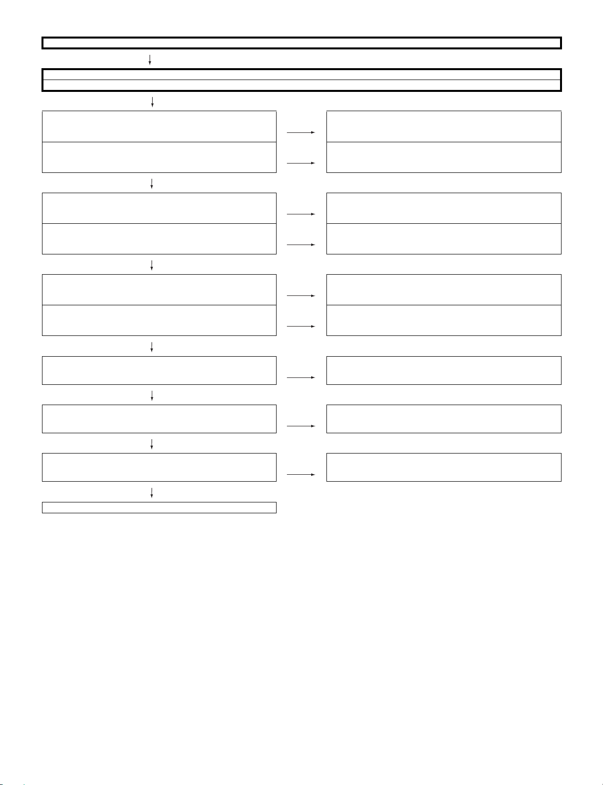
LC-65RX1M
<External input INPUT1,INPUT2> No picture on the display (5)
Does not the picture of the component video signal input to INPUT1 go out?
Does not the picture of the component video signal input to INPUT2 go out?
TERMINAL UNIT:
<INPUT1>
Is COMPONENT1 signal sent to pins (6)/Y, (5)/Pb and (4)/Pr of
COMPONENT1 (J1705)?
<INPUT2>
Is COMPONENT2 signal sent to pins (6)/Y, (5)/Pb and (4)/Pr of
COMPONENT2 (J1703)?
YES
<INPUT1>
Is COMPONENT1 signal sent to pins (21)/Y, (23)/Pb and (25)/Pr
of IC506?
<INPUT2>
Is COMPONENT2 signal sent to pins (27)/Y, (29)/Pb and (31)/Pr
of IC506?
YES
<INPUT1>
Is detection signal COMP1_PLUG of the COMPONENT video
signal from pin (7) of the input terminal J1705 normal?
<INPUT2>
Is detection signal COMP2_PLUG of the COMPONENT video
signal from pin (7) of the input terminal J1703 normal?
NO Check the setting of an external input device that connects of
J1705.
NO Check the setting of an external input device that connects of
J1703.
NO Check the line between J1705 and IC506.
NO Check the line between J1703 and IC506.
NO Check from the input terminal J1705 to pin (38) of IC506.
NO Check from the input terminal J1703 to pin (40) of IC506.
YES
Is COMPONENT signal output from pin (60)/Y, (59)/Pb, and (58)/
Pr of IC506 to pin (6), (8), and (10) of connector (SC501)?
MAIN UNIT: YES
Is COMPONENT signal output from pins (6), (8), (10) of connec-
tor (SC1101)?
YES
Is COMPONENT signal input into pins (W6), (Y9), (W8) of
IC3301 (VIDEO_PROCESSOR)?
YES
Refer to “The picture doesn't appear in all modes.”
NO Check the line between IC506 and SC501.
(Q516, Q518, Q520, etc.)
NO Check the connector. (SC501/SC1101)
NO Check the line between SC1101 and IC3301.
6 – 9
Page 71

LC-65RX1M
<When INPUT3 is used for external input> No picture on the display (6)
Does not the picture of the composite video signal input to INPUT3 go out?
MINI-AV UNIT:
Is CVBS signal output from pin (6) in input terminal J901 to pin
(5) of connector P901?
TERMINAL UNIT: YES
Is the CVBS signal input from pin (5) of connector P501 to pin (3)
of IC506 (VIDEO SELECTOR)?
YES
Is the composite video signal detection signal V3_PLUG signal
from pin (7) of the input terminal J901 normal?
YES
Is the V3_PLUG signal input to pin (2) of IC506? NO Check the between V3_PLUG_LINE J901 and pin (2) of TERMI-
YES
Is video signal MAIN_Y/V output into pin (2) of connector SC501
from pin (52) of IC506?
NO Check the line between J901 and P901.
NO Check the line between P501 and IC506.
(Connector P901/P501, etc.)
NO Check J901 or peripheral circuits.
NAL UNIT's IC506. (ConnectorP901/P501,etc)
NO Check the line between IC506 and SC501.
TERMINAL UNIT: YES
Is picture signal MAIN_Y/V input to pin (2) of connector SC1101? NO Check the connector. (SC501/SC1101)
YES
Is picture signal MAIN_Y/V input to pin (Y4) of IC3301
(VIDEO_PROCESSOR)?
YES
Refer to “The picture doesn't appear in all modes.”
NO Check the line between SC1101 and IC3301.
6 – 10
Page 72

LC-65RX1M
<When INPUT3 is used for external input> No picture on the display (7)
Does not the picture of the Y/C video signal input to INPUT3 go out?
MINI AV_UNIT:
Is Y/S signal input into pin (13), (11) of connector P901 from pin
(3)/Y, (4)/C of J902?
TERMINAL UNIT: YES
Is Y/C signal input into pin (5), (7) of IC506 (VIDEO SELECTOR)
from pin (13)/Y, (11)/C of connector P501?
YES
Is the Y/C video signal detection function S3_PLUG signal from
pin (6) of the input terminal J902 normal?
YES
Is the S3_PLUG signal input to pin (42) of IC506? NO Check the between S3_PLUG_LINE J902 and pin (42) of TER-
YES
Is Y/C signal output into pin (2), (4) of connector SC501 from pin
(52)/Y, (50)/C of IC506?
NO Check the line between J901 and P901.
NO Check the line between P501 and IC506.
(Connector P901/P501, etc.)
NO Check J902 or peripheral circuits.
MINAL UNIT’s IC506. (connector P901/P501, etc.)
NO Check the line between IC506 and SC501.
MAIN UNIT: YES
Is Y/C signal input to pin (2), (4) of connector SC1101? NO Check the connector. (SC501/SC1101)
YES
Is Y/C signal input to pin (Y4), (V9) of IC3301
(VIDEO_PROCESSOR)?
YES
Refer to “The picture doesn’t appear in all modes.”
NO Check the line between SC1101 and IC3301.
6 – 11
Page 73

<When INPUT4 is used for external input> No picture on the display (8)
Does not the picture of the HDMI signal input to INPUT4 go out?
MINI AV_UNIT:
Is the HOT_PLUG detection function of pin (19) of a HDMI terminal (SC801) normal?
YES
Are EDID data pin (6)/SCL of IC801 (EEPROM), pin (5) / SDA
accessed, and is it read from pin (15), (16) of a HDMI terminal
(SC801)?
YES
Is TMDS signal input into pin (32, 33)/RXC±, (35, 36)/RX0±, (38,
392)/RX1±, (1, 2)/RX2± of IC802 (HDMI_BUFFER) from SC801?
YES
Is TMDS signal output into pin (11, 12), (8, 9), (5, 6), (2, 3) of the
connector SC803 from pin (18, 19)/CLK±, (15, 16)/DAT0±, (12,
13)/DAT1±, (9, 16)/DAT2± of IC802?
LC-65RX1M
NO Check the between pin (56) of IC1507 and pin (19) of SC801.
Check the connection and setup with the external HDMI devices.
NO Is access possible in the re-writing or exchange of EDID data of
IC801?
NO
Check SC801, IC802, IC803 and peripheral circuits.
NO Check the line between SC801 and IC802.
NO Check the line between IC802 and SC803.
YES
Is TMDS signal input into pin(59,58)/TMDS6_CLK±, (62, 61)/
TMDS6_D0±, (65, 64)/TMDS6_D1±, (68, 67)/TMDS6_D2± of
IC1507?
YES
Is each signal output from pin (10, 11)/TMDS_CLKP/N, (7, 8)/
TMDS_D0P/N, (4, 5)/TMDS_D1P/N, (1, 2)/TMDS_D2P/N, (77,
78)/SDA_SINK/SCL_SINK, (79)/DDC5VOR_A of IC1507?
YES
Is each signal of IC3301 (VIDEO_PROCESSOR) pin (L1, L2)/TMDS_CLKP/N, (M1, M2)/TMDS_D0P/N, (N1, N2)/TMDS_D1P/N, (P1, P2)/
TMDS_D2P/N, (T11, U11)/SDA_SINK/SCL_SINK, (T10)/DDC5VOR_A input?
YES NO
Refer to “The picture doesn't appear in all modes.” Check the line between SC1101 and IC3301.
NO Check the line between connector (SC803) and IC1507.
(SC803, SC1503 and Wire harness (HM))
NO Is the control signal named IC1507 and IC9101 (CPLD) normal?
(HDMI_SW_INT, HDMI_RST, etc.)
6 – 12
Page 74

LC-65RX1M
<When INPUT5/6 is used for external input> No picture on the display (9)
Does not the picture of the HDMI signal input to INPUT5/6 go out?
MAIN UNIT:
INPUT5
Is the HDMI detection function output from pin (19) of the HDMI
terminal (SC1501) normal?
INPUT6
Is the HDMI detection function output from pin (19) of the HDMI
terminal (SC1502) normal?
YES
INPUT5
Is EDID data pin (6)/SCL, pin (5)/SDA of IC1501 (EEPROM)
accessed, and is it read from pin (15), (16) of a HDMI terminal
(SC1501) pin(15), (16)?
NO INPUT5
Check between SC1501and IC1507(HDMI_SW)of pin(16).
(IC1506, etc.)
NO INPUT6
Check between SC1502 and IC1507(HDMI_SW) of pin(36).
(IC1506, etc.)
YES
Check the connection and setup with the external HDMI devices.
NO Is access possible in the re-writing or exchange of EDID data of
IC1501?
NO
Check the circumference circuit of SC1501, IC1501and IC1507.
INPUT6
Is EDID data pin (6)/SCL, pin (5)/SDA of IC1502 (EEPROM)
accessed, and is it read from pin (15), (16) of a HDMI terminal
(SC1501) pin (15), (16)?
YES
INPUT5
Is TMDS signal input into pin (19, 18)/TMDS2_CLKP/N±,
(22, 21)/TMDS2_D0P/N, (25, 24)/TMDS2_D1P/N, (28, 27)/
TMDS2_D2P/N of IC1507 from SC1501?
INPUT6
Is TMDS signal input into pin (39, 38)/TMDS1_CLKP/N±, 42, 41)/
TMDS1_D0P/N, (45, 44)/TMDS1_D1P/N, (48, 47)/TMDS1_D2P/
N of IC1507 from SC1502?
YES
Is each signal output from pin (10, 11)/TMDS_CLKP/N, (7, 8)/
TMDS_D0P/N, (4, 5)/TMDS_D1P/N, (1, 2)/TMDS_D2P/N, (77,
78)/SDA_SINK/SCL_SINK, (79)/DDC5VOR_A of IC1507?
YES
Is each signal of IC3301 (VIDEO_PROCESSOR) pin (L1, L2)/TMDS_CLKP/N, (M1, M2)/TMDS_D0P/N, (N1, N2)/TMDS_D1P/N, (P1, P2)/
TMDS_D2P/N, (T11, U11)/SDA_SINK/SCL_SINK, (T10)/DDC5VOR_A input?
YES NO
Refer to “The picture doesn't appear in all modes.” Check the line between IC1507 and IC3301.
NO Is access possible in the re-writing or exchange of EDID data of
IC1502?
NO
Check the circumference circuit of SC1501, IC1501and IC1507.
NO Check the line between SC1501 and IC1507.
NO Check the line between SC1502 and IC1507.
NO Is the control signal of IC1507 and IC9101 (CPLD) normal?
(HDMI_SW_INT, HDMI_RST, etc.)
6 – 13
Page 75
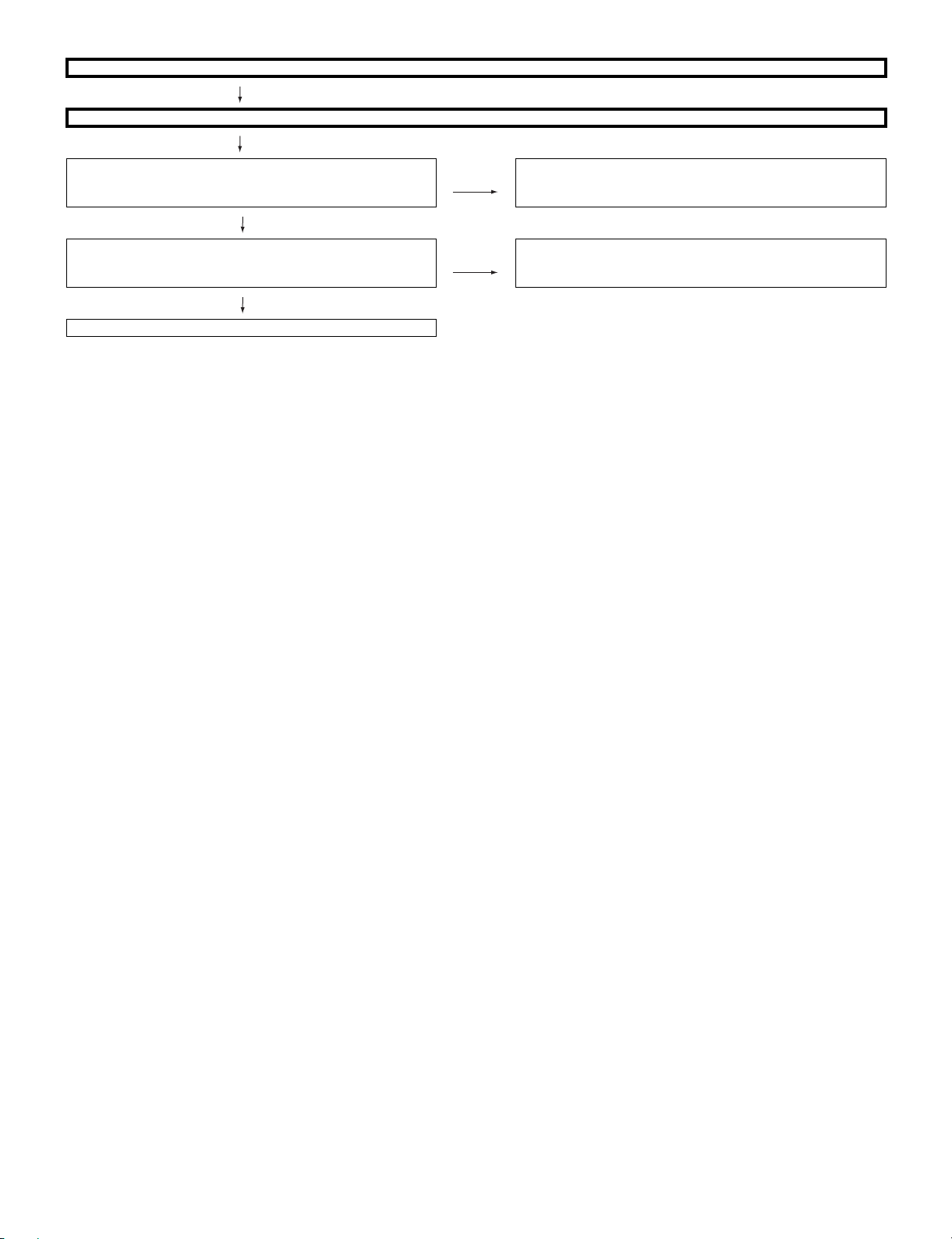
<When INPUT7 is used for external input> No picture on the display (10)
Does not the picture of the DVI(ANALOG) video signal input to INPUT7(15pin-D-SUB terminal) go out?
MAIN_UNIT:
Are the video signal and the synchronized signal input from pin
(1, 2, 3)/(R, G, B), (13 and 14)/(V, H) of input terminal D-SUB
(SC1504)?
NO
Are the video signal and the synchronized signal input from pin
(U8, Y7, W10)/ (R, G , B), pin (V10, U10)/(H, V) of IC3301 (VIDEO
PROCESSOR)?
NO
Refer to “The picture doesn't appear in all modes.”
YES Check the connection and setup between SC1504 and its cir-
cumference circuit as well as the external HDMI devices.
(IC1503, etc.)
YES Check the line between SC1504 and IC3301.
LC-65RX1M
6 – 14
Page 76

LC-65RX1M
<During external connection> No picture on the monitor (1)
No picture appears on MONITOR OUT1 - connected monitor during the tuner (U/V) reception.
Checklist:
1) Is ANT-CABLE disconnected or connected improperly? ⋅ ⋅ ⋅ Connect it correctly as per the operation manual.
2) The picture is sent to the monitor in a CVBS signal if the source during display is TV, CVBS or Y/C of INPUT1-3.
When sent by component, etc., that signal is not sent to the monitor.
3) When the monitor picture is not sent and is not displayed on the monitor, refer to “No picture” for each terminal.
TERMINAL UNIT:
Is CVBS signal output into pin (6) of J1701 (MONITOR OUT1)
from pin (51) of IC506?
NO
Is TUNRECVBS signal output from pin (5) of IC7508? YES Check the line between IC7508 and IC503.
NO
Is IF signal output from pin (11) of TU7501? YES Check the line between IC7508 and TU7501.
YES Check the setting of an external input device that connects of
J1701.
NO
Check whether I2C is normally accessed between TU7501.
<During external connection> No picture on the monitor (3)
SCART2:
No picture from INPUT1, INPUT2 appears on MONITOR OUT-connected monitor.
Checklist:
1) The picture is sent to the monitor in a CVBS signal if the source during display is TV, CVBS or Y/C of INPUT1-3.
When sent by component, etc., that signal is not sent to the monitor.
2) When the monitor picture is not sent and is not displayed on the monitor, refer to “No picture” for each terminal.
TERMINAL UNIT:
Is CVBS signal input from pin (51) of IC506 to pin (6) of J1701? YES Check the setting of an external input device that connects of
J1701.
NO
Is CVBS signal sent to pin INT_V/(65) or IN2_V/(71) of IC506
(VIDEO_SELECTOR)?
NO
Is CVBS signal sent to pin (8) of INPUT1 (J1704) or pin (8) of
INPUT2 (J1702)?
YES Check the IC506 and its peripheral circuits.
YES Check the line between J1702/J1704 and IC506.
NO
Check the setting of an external input device that connects of
J1702/J1704.
6 – 15
Page 77

<During external connection> No picture on the monitor (4)
V
SCART2:
No picture from INPUT3 appears on MONITOR OUT- connected monitor.
Checklist:
1) The picture is sent to the monitor in a CVBS signal if the source during display is TV, CVBS or Y/C of INPUT1-3.
When sent by component, etc., that signal is not sent to the monitor.
2) When the monitor picture is not sent and is not displayed on the monitor, refer to “No picture” for each terminal.
TERMINAL UNIT:
Is CVBS signal input from pin (51) of IC506 to pin (6) of
MONITOR OUT (J1701)?
YES Check the setting of an external input device that connects of
J1701.
NO
Is CVBS signal input from pin (5) of the connector P501 to pin (3)
YES Check the IC506 and its peripheral circuits.
of IC506 (VIDEO SELECTOR)?
MAIN UNIT: NO
Is CVBS signal input from pin (6) of the input terminal J901 to pin
YES Check the connector (P501/P901)
(5) of the connector (P501)?
NO
Is V3_PLUG signal of the CVBS signal detection function from
pin (7) of the input terminal J901 normal?
YES Check the setting of an external input device that connects of
J901.
LC-65RX1M
NO
Check between V3_PLUG_LINE J901 and pin (2) of IC506 in the
TERMINAL UNIT. (Connector P901/P501, etc.)
LED flashing atterns for error notification
250ms 1sec
1) Power red LED Remarks
Error type Power red LED operation (1 cycle) Description
Lamp failure
Flashes once: Fast L: Off
Power failure
Flashes twice L: Off
Communication failure H: On Refer to "Communication failure details".
with main CPU Communication line failure or main CPU(IC8101) communication failure. ψ Check main CPU (IC8101).
Flashes 3 times L: Off
Monitor temp. failure
Flashes 5 times L: Off
2) Power failure details (Power LED flashes twice and OPC LED flashes) Remarks
Error type OPC LED operation (1 cycle) Description
PS_ON AC_DET(IC2002_16pin): Abnormal (L). Main converter 12V is not applied.
12V failure
Flashes once L: Off
PS_ON DET_10V(IC2002_57pin): Abnormal (L). Main power UR15V is not applied.
10V failure
Flashes 3 times L: Off
D_POW DET_D3V3(IC2002_59pin): Abnormal (L). D3.3V is not applied.
Digital 3.3V failure
Flashes 4 times L: Off
PANEL_POW DET_PNL5V(IC2002_58pin): Abnormal (L). Panel power is not applied.
Panel 5V failure
Flashes 5 times L: Off
Main failure
Flashes 7 times L: Off
3) Communication failure details (Power LED flashes 3 times and OPC LED flashes)
Error type OPC LED operation (1 cycle) Description
Initial communication H: On
reception failure
Flashes once L: Off
Start-up confirmation H: On
reception failure
Flashes twice L: Off
Regular communication
failure
Flashes 3 times L: Off
Restart failure
Flashes 4 times L: Off
H: On
H: On Refer to "Power failure details".
H: On
H: On
H: On
H: On
H: On
H: On
H: On
H: On
ERR_PNL(IC2002_43pin): Abnormal L. Confirmed after 5 consecutive detections at 1 second intervals (detected
Note that after five detection counts, the lamp cannot be activated except in the monitoring process. (For
Accumulated counts are cleared to 0 when the corresponding setting in the process A is made, when the power
If the panel temperature is 60 C or more for 15 seconds or more in a row, CAUTION appears on the OSD of AVC
If the panel temperature is 60 C or more for 15 seconds or more in a row, error standby is activated.
(MONITOR MAX TEMP of process adjustment (28/31): Change of temperature failure AD value): Thermistor
If error is detected during operation, the power is turned on again by interrupt handling (instantaneous bl
If error is detected during start-up or operation, the power is turned on again by polling.
If error is detected during start-up or operation, the power is turned on again by polling.
If error is detected during start-up or operation, the power is turned on again by polling.
Main microprocessor detection error
The details are displayed on page 1 of process adjustment for the main microprocessor (IC8101).
Remarks
Initial communication from the main CPU (IC8101) is not received.
ψ Communication line failure or main CPU (IC8101) start-up failure
Start-up reason confirmation from the main CP(IC8101) is not received.
ψ Main CPU (IC8101) start-up failure or monitor microprocessor (IC2002) reception failure
Regular communication that is performed at 1 second intervals in the normal operation is interrupted.
ψ Main CPU (IC8101) operation failure or monitor microprocessor (IC2002) reception failure
When restarted by a software with the standby off/on, restart completion notification is not received.
ψ Main CPU (IC8101)restart failure to monitor microprocessor (IC2002) reception failure
6 – 16
Page 78

LC65RX1M
LC65RX1M
CHAPTER 7. MAJOR IC INFORMATIONS
ServiceManual
[1] MAJOR IC INFORMATIONS
1. MAJOR IC INFORMATIONS
1.1. IC7503 (VHiTDA9886+-1Y)
The TDA9886 is an alignment-free multistandard (PAL, SECAM and NTSC) vision and sound IF signal PLL demodulator for positive and negative
modulation, including sound AM and FM processing.
1.2. IC506 (VHiMM3151XQ-1Q)
This video switch controlled by the I2C bus is used to switch between component signal, S-video signal and composite signal.
The signal group input from each input terminal and the tuner is selected by the control signal of the I2C bus.
The selected output signal is fed to IC3301 (IXC010WJ) of the video processor circuit.
1.3. IC1402 (VHiR2A15505-1Y)
R2S15502SP is a Sound Multiplex Decoder IC.
It supports the NICAM and A2 system.
It incorporates the high-speed ADC, and all processings are digitally implemented including demodulation.
1.4. IC1403 (VHiTAS3108D-1Y)
This IC is an audio processor for the digital TV and a 1-chip IC equipping the DSP only for audio with the AD/DA converter.
The 48bit DSP core has a processing capability of 135MHz and 675MIPS and realizes the high-quality audio processing.
1.5. IC1404 (VHiAK4683EQ-1Q)
1-chip 24bit CODEC (COmpression/DECompression) with a built-in 2ch ADC and 4ch ADC. The ADC has the enhanced dual bit architecture to realize the wide dynamic range. The DAC adopts the newly-developed advanced multi-bit architecture to achieve wider dynamic range and low outband
noise. It also incorporates the digital audio receiver (DIR) and transmitter ( DIT) compatible with 192kHz and 24bit. The DIR automatically detects
Non-PCM data stream such as Dolby Digital (AC-3). For the digital audio output, ADC output or external digital input can be selected. The control is
set through the serial µP I/F.
1.6. IC1301 (VHiYDA147SZ-1Y)
High-efficiency digital audio power amplifier IC with maximum power output of 20W (Vddp=14V, RL=4Ω) x 2ch.
It incorporates the “DRC (Dynamic range compression)” function. Since the volume is increased at low volume level and is decreased at high volume
level, it is possible to prevent sudden volume change. It is also provided with the “power limiter” which can set the output limit.
1.7. IC402 (VHiBD9305AF-1Y)
1ch step-down switching regulator control
It supplies a power supply voltage of +5.0V.
1.8. IC9601/9603/9604/9606 (VHiTPS40055-1Y)
DC/DC converter IC. It supplies power supply voltages of 3.3/1.8/1.3/1.2V.
This IC has various user programming functions such as operation frequency, soft-start time, voltage feed forward, high-side current limit, and exter-
nal loop compensation. It is also provided with the stabilized 10V gate drive power supply for the boot strap charging circuit of the high-side N channel
MOSFET and the driver for the low-side synchronous rectification MOSFET.
1.9. IC9602 (VHiMP2367DE-1Y)
Monolithic step down regulator.
It supplies a power supply voltage of D5.0V.
• Programmable Soft-Start.
• Fixed 340kHz frequency.
• Cycle-by-Cycle over current protection.
• Input Under Voltage Lockout.
7 – 1
Page 79

1.10. IC1507 (VHiSii9185A-1Q)
Sil9185 is a 3-input/1-output switch compatible with HDMI1.3.
• Built in Consumer Electronics Control (CEC) support
• Individual control of Hot Plug Detect (HPD) for each port
• 5V detect to help speed soft mute of audio during plug-in, plug-out conditions
• Control via local I2C bus.
• Supports video resolutions up to 1080p, 60Hz, 12-bit or 720p/1080i, 120Hz, 12-bit
• Built-in adaptive equalizer provides long cable support even at deep color resolutions
• Pre-emphasis in transmitter
• DVI 1.0, HDCP 1.1 and HDMI 1.3 compliant receiver and transmitter
1.11. IC9101 (RH-iXC121WJQZQ)
This IC performs the CPLD (Complex Programmable Logic Device) RESET, I/O and Bus control.
1.12. IC8101 (RH-iXC011WJQZQ)
HIDTVPro-LX Digital AV decoder & Main CPU.
• Master CPU with MMU.
• DDR2 memory up to 256mHz.
• Two Transport stream inputs, DVB compliant.
• Two HD MPEG2 video decoders.
• Demux, supports two TS inputs and one PS input.
• DVB_CI, up to two PCMCIA slots for CAM cards.
• DVB/DES.
• AC3/MPEG2/MP3/AAC ⋅ ⋅ ⋅ audio.
• 1920 x 1080p de-interlacing.
• Graphics engine.
• Two video planes and graphics planes with Alpha blender, overlay, scrolling, flashing, colour key, ARB support.
• Smart-Cards/UART/infrared IR/RTC/two HW timers/interrupt/Key button ADCs.
• Flash/IDE/PCI Host.
• Audio interface: AC97 link/I2S_out/I2S_in/SPDIF and lip-sync.
• Digital 24-bit RGB/YUV inputs.
• Dual port/Single port LVDS output.
• USB2.0 HOST/PHY built with EHCI.
• CVBS/S-video/YCbCr output.
• Two HD, 1920 x 1080p.
LC65RX1M
1.13. IC8701 (VHiS29G128P-1Q)
128Mbit Flash memory.
3.0V single power supply, page mode flash memory. It memorizes the program and broadcast data area.
1.14. IC8702 (RH-iXC150WJQZY)
The ICS275 field programmable VCXO clock synthesizer generates up to four high-quality, high-frequency clock outputs including multiple reference
clocks from a low-frequency crystal input. Using ICS’ VersaClockTM software to configure PLLs and outputs, the ICS275 contains a One-Time Programmable (OTP) ROM for field programmability. Programming features include VCXO, eight selectable configuration registers and up to two sets of
two low-skew outputs.
Using Phase-Locked Loop (PLL) techniques, the device runs from a standard fundamental mode, inexpensive crystal, or clock.
1.15. IC8301-4 (RH-iXC154WJQZQ)
4M x 16Bit x 4 Banks graphic DDR2 Synchronous DRAM with Differential Data Strobe.
Program, DTV video buffer.
7 – 2
Page 80

LC65RX1M
1.16. IC3301 (RH-iXC010WJN1Q)
SVP-WX Video Processor.
• Integrated HDMI Receiver
• Integrated De-interlacing
• Integrated ADC
• SRC (Scan Rate Conversion) Improvement
• PC Auto Tune
• Built-in LVDS Transmitter
• Scaling Engine
• DNR-Digital Noise Reduction Filter
• Advanced Chroma Processing
• Color Management
• RCR (Real Color Reproducer)
• Dynamic Contrast Improvement
• Integrated 3D Digital Comb Video Decoder with Programmable Filter
• Inverse Color Space Conversion (ICSC)
• Frame Rate Conversion
• Fast Blank
• Built-in ADC to decode one FB and two FS signals to support dual SCART solutions
• Teletext
• Memory Interface
• DCR Advanced Image Processing
• Multi Screen Display Mode
• OSD and VBI/Closed Caption
• Advanced OSD Engine
1.17. IC3501-2 (RH-iXC163WJQZQ)
1M x 32Bit x 4 Banks Double Data Rate Synchronous DRA with Bi-directional Data Strobe and DLL.
Video buffer.
1.18. IC2002 (RH-iXB986WJQZQ)
The monitor microprocessor is intended to communicate with the main microprocessor and to operate the system. It also controls power of the entire
system.
7 – 3
Page 81
LC65RX1M
2. Detailed ICs Information
2.1. IC402 (VHiBD9305AF-1Y)
2.1.1 Pin Connections and short description
Pin No. Pin Name I/O Pin Function
1 RT — Timing resistor external terminal
2 CT — Timing capacitor external terminal
3 ENB I Control input terminal
4 GD O Gate drive output terminal
5 VCC — Power terminal
6 GND — Ground terminal
7 COMP O Error amplifier output terminal
8 FB I Error amplifier inversion input terminal
2.2. IC506 (VHiMM3151XQ-1Q)
2.2.1 Pin Connections and short description
Pin No. Pin Name I/O Pin Functio n
69 C1 I Chroma signal input
75 C2 I
1C3 I
7C4 I
70 S1 I The terminal which detects the connection state of S-connector.
76 S2 I
2S3 I
65 V1 I Composite signal input.
71 V2 I
77 V3 I
3V4 I
9V5 I
15 V6 I
68 S2-1 I The terminal which detects the aspect ratio information of S-connector.
74 S2-2 I
80 S2-3/ FS3 I The terminal which detects the aspect ratio information of S-connector, or which detects
the voltage of FS pin of a scart connector.
67 Y1 I Luminance signal input.
73 Y2 I
79 Y3 I
5Y4 I
14 ADR I Slave address select pin.
16 BIAS I BIAS
32 L13 I The terminal which detects the number of scanning lines information on D-connector.
20 L11/ FS1 I The terminal which detects the number of scanning lines information on D-connector, or
26 L12/ FS2 I
21 CY1 I Component Y-signal input.
27 CY2 I
33 CY3 I
22 L21 I The terminal which detects the I/P information of D-connector.
28 L22 I
34 L23 I
24 L31 I The terminal which detects the aspect ratio information of D-connector.
30 L32 I
36 L33 I
23 PB1 I Colour difference PB-signal input.
29 PB2 I
35 PB3 I
25 PR1 I Colour difference PR-signal input.
31 PR2 I
37 PR3 I
38 SW1 I The terminal which detects the connection state of D-connector.
40 SW2 I
42 SW3 I
45 SDA I/O Data I/O of I2C bus
46 SCL I Clock input of I2C bus
which detects the voltage of FS pin of a scart connector.
7 – 4
Page 82

LC65RX1M
Pin No. Pin Name I/O Pin Functio n
49 DCOUT O DC output for S-terminal.
51 VOUT3 O Monitor output (composit signal)
50 COUT3/VOUT6 O Monitor output (Chroma or composite signal)
52 YOUT3/ VOUT5 O Monitor output (Luminance or composite signal)
54 PROUT2 O Colour difference PR-signal output.
58 PROUT1 O
55 PBOUT2/ COUT2 O Colour difference PB-signal or chroma signal output.
59 PBOUT1/ COUT1 O
56 CYOUT2/ YOUT2/ VOUT2 O Colour difference signal, Luminance or composite signal output.
60 CYOUT1/ YOUT1/ VOUT1 O
64 O1 O Output port.
66 O2 O
72 O3 O
78 O4 O
53, 57 VDD1 — Power supply (+9V)
8, 47 VDD2 — Power supply (+5V)
18, 44, 62 GND — Ground
4, 6, 10, 1 1, 12, 13,
17, 19, 39, 41, 43,
48, 61, 63
2.3. IC1301 (VHiYDA147SZ-1Y)
2.3.1 Block Diagram
NC — Unconnected pins.
7 – 5
Page 83

2.3.2 Pin Connections and short description
Pin No. Pin Name I/O Pin Function
1, 2, 12, 25, 35, 36 NC — No connection
3 PVDDREG — Power terminal for regulator (PVDD)
4 AVDD — Output terminal for 3.3V regulator
5 INLP I Analog input terminal (Lch+)
6 INLM I Analog input terminal (Lch-)
7 VREF VREF terminal
8 INRM I Analog input terminal (Rch-)
9 INRP I Analog input terminal (Rch+)
10 AVSS — GND terminal for analog
11 PLIMIT I Power limit setting terminal
13, 14 PVDDPR — Power terminal for digital amplifier output (Rch+)
15, 16, 17 OUTPR O Digital amplifier output terminal (Rch+)
18, 19 PVSSR — Ground terminal for digital amplifier output (Rch)
20, 21, 22 OUTMR O Digital amplifier output terminal (Rch-)
23, 24 PVDDMR — Power terminal for digital amplifier output (Rch-)
26 SLEEPN I Sleep control terminal
27 PROTN O Error flag output terminal
28 MUTEN I Mute control terminal
29 CKOUT O Clock output terminal for synchronization
30 CKIN I External clock input terminal
31 NCDRC0 I Non-clip/DRC1/DRC2 mode selection terminal 0
32 NCDRC1 I Non-clip/DRC1/DRC2 mode selection terminal 1
33 GAIN0 I GAIN setting terminal 0
34 GAIN1 I GAIN setting terminal 1
37, 38 PVDDML — Power terminal for digital amplifier output (Lch-)
39, 40, 41 OUTML O Digital amplifier output terminal (Lch-)
42, 43 PVSSL — Ground terminal for digital amplifier output (Lch)
44, 45, 46 OUTPL O Digital amplifier output terminal (Lch+)
47, 48 PVDDPL — Power terminal for digital amplifier output (Lch+)
LC65RX1M
2.4. IC1402 (VHiR2A15505-1Y)
2.4.1 Pin Connections and short description
Pin No. Pin Name I/O Pin Function
1 AVSS — 0V Power Supply for Analog Core
2 AVDD — 3.3V Power Supply for Analog Core
3 SIF I Sound IF Input
4 VREF1 — ADC Voltage Reference 1
5 VREF2 — ADC Voltage Reference 2
6 TEST I Test pin
7 XI I Crystal Oscillator Input
8 XO O Crystal Oscillator Output
9 IVDD — 3.3V Power Supply for I/O Buffer
10 IVSS — 0V Power Supply for I/O Buffer
11 DVSS — 0V Power Supply for Logic Core
12 DVDD — 1.5V Power Supply for Logic Core
13 DACCLK I/O DAC Clock
14 BCK I/O Bit Clock
15 LRCK I/O LR Clock
16 SD0 O Digital Output for External DAC
17 SDI I Digital Input for Internal DAC
18 SDA I/O I2C bus Serial Data
19 SCL I I2C bus Serial Clock
20 STATUS I/O PLL Setting / Status Signal
21 RESET I Hardware Reset (Active low)
22 ROUT O Rch Analog Output
23 VCOM — DAC Voltage Reference
24 LOUT O Lch Analog Output
7 – 6
Page 84

LC65RX1M
2.5. IC1403 (VHiTAS3108D-1Y)
2.5.1 Block Diagram
2.5.2 Pin Connections and short description
Pin No. Pin Name I/O Pin Function
38 AVDD — Analog power-supply input (3.3V)
1 AVSS — Analog ground
7 CS0 I Pull-down Chip select
9, 30 DVDD — Digital power-supply input (3.3V)
10, 29 DVSS — Digital ground
8 GPIO I/O Pull-up GPIO control pin (user programmable)
19 LRCLK I/O Pull-down Sample rate clock (fS) input or output
5 MCLKIN I Master clock input (Connect to ground when not in use.)
21 MCLKO O Master clock output
6 MICROCLK_DIV I Pull-down Internal microprocessor clock divide control
31 PDN I Pull-up Powers down all logic and stops all clocks, active-low. Coefficient memory remains stable
34 PLL0 I Pull-up PLL control 0
35 PLL1 I Pull-down PLL control 1
36 PLL2 I Pull-down PLL control 2
33, 37 RESERVED — Connect to ground
32 RESET I Pull-up Reset, active-low
16 SCL1 I/O I2C port #1 clock (always a slave)
18 SCL2 I/O I2C port #2 clock (always a slave)
20 SCLKIN I Pull-down Bit clock input
through power-down cycle.
7 – 7
Page 85

Pin No. Pin Name I/O Pin Function
22 SCLKOUT1 O Bit clock #1 out. Used to receive input serial data.
23 SCLKOUT2 O Bit clock #2 out. Used to clock output serial data.
15 SDA1 I/O I2C port #1 data (always a slave)
17 SDA2 I/O I2C port #2 data (always a slave)
11 SDIN1 I Pull-down Serial data input 1
12 SDIN2 I Pull-down Serial data input 2
13 SDIN3 I Pull-down Serial data input 3
14 SDIN4 I Pull-down Serial data input 4
27 SDOUT1 O Serial data output 1
26 SDOUT2 O Serial data output 2
25 SDOUT3 O Serial data output 3
24 SDOUT4 O Serial data output 4
2 VR_PLL — Internal regulator. This pin must not be used to power external devices.
3 XTALI I Oscillator input (connect to ground when not in use)
4 XTALO O Oscillator output
28 VR_DIG --- Internal regulator. This pin must not be used to power external devices.
2.6. IC1404 (VHiAK4683EQ-1Q)
2.6.1 Block Diagram
LC65RX1M
7 – 8
Page 86

LC65RX1M
2.6.2 Pin Connections and short description
Pin No. Pin Name I/O Pin Function
1 PVDD — PLL Power supply, 4.5V~5.5V.
2 RX0 I Receiver Channel 0 (Internal biased pin. Internally biased at PVDD/2).
3 I2C I Control Mode Select.
4 RX1 I Receiver Channel 1.
5 RX2 I Receiver Channel 2.
6 RX3 I Receiver Channel 3.
7 INT O Interrupt
8 DZF O Zero Input Detect.
9 CDTO O Control Data Output in Serial Mode and I2C pin = “L”.
10 LRCKB I/O Channel Clock B
11 BICKB I/O Audio Serial Data Clock B
12 SDTOB O Audio Serial Data Output B
13 OLRCKA I/O Output Channel Clock A
14 ILRCKA I/O Input Channel Clock A
15 BICKA I/O Audio Serial Data Clock A
16 SDTOA O Audio Serial Data Output A
17 MCKO O Master Clock Output
18 TVDD — Output Buffer Power Supply, 2.7V~5.5V
19 DVSS — Digital Ground
20 DVDD — Digital Power Supply, 4.5V~5.5V
21 XTI I X’tal Input
22 XTO O X’tal Output
23 TX O Transmit Channel Output
24 MCLK2 I Master Clock Input
25 PDN I Power-Down Mode & Reset
26 SDA I/O Control Data in Serial Mode and I2C pin = “H”.
27 SCL I Control Data Clock in Serial Mode and I2C pin = “H”.
28 CSN I Chip Select in Serial Mode and I2C pin = “L”.
29 SDTIA1 I Audio Serial Data Input A1
30 SDTIA2 I Audio Serial Data Input A2
31 SDTIA3 I Audio Serial Data Input A3
32 SDTIB I Audio Serial Data Input B
33 HVDD — HP Power Supply, 4.5V~5.5V
34 HVSS — HP Ground
35 HPR O HP Rch Output.
36 HPL O HP Lch Output.
37 MUTET — HP Common Voltage Output
38 LOUT2 O DA C2 Lch Positive Analog Output
39 ROUT2 O DAC2 Rch Positive Analog Output
40 LOUT1 O DA C1 Lch Positive Analog Output
41 ROUT1 O DAC1 Rch Positive Analog Output
42 VCOM — DAC/ADC Commo n Voltage Output
43 AVDD2 — DAC Power Supply, 4.5V~5.5V
44 AVSS2 — DAC Ground
45 LISEL O Lch Feedback Resistor Output
46 LOPIN O Lch Feedback Resistor Input. 0.5 x AVDD1.
47 ROPIN O Rch Feedback Resistor Input. 0.5 x AVDD1.
48 RISEL O Rch Feedback Resistor Output
49 AVSS1 — ADC Ground
50 AVDD1 — ADC Power Supply, 4.5V~5.5V
51 LIN1 I Lch Input 1
52 RIN1 I Rch Input 1
53 LIN2 I Lch Input 2
54 RIN2 I Rch Input 2
55 LIN3 I Lch Input 3
56 RIN3 I Rch Input 3
“L”: 4-wire Serial, “H”: I2C Bus
When the input data of DAC follow total 8192 LRCK cycles with “0” input data, this pin goes to “H”. And
when RSTN1 bit is “0”, PWDA bit is “0”, this pin goes to “H”
When DIT bit = “0”, RX0~3 Through.
When DIT bit = “1”, Internal DIT Output.
When “L”, the AK4683 is powered-down, all registers are reset. And then all digital output pins go “L”.
The AK4683 must be reset once upon power-up.
7 – 9
Page 87

Pin No. Pin Name I/O Pin Function
57 LIN4 I Lch Input 4
58 RIN4 I Rch Input 4
59 LIN5 I Lch Input 5
60 RIN5 I Rch Input 5
61 LIN6 I Lch Input 6
62 RIN6 I Rch Input 6
63 PVSS — PLL Ground
64 R — External Resistor
2.7. IC1507 (VHiSii9185A-1Q)
2.7.1 Block Diagram
LC65RX1M
7 – 10
Page 88

LC65RX1M
2.7.2 Pin Connections and short description
Pin No. Pin Name I/O Pin Function
System Switching Pins
30, 50, 70 DSDA0, DSDA1, DSDA2 I/O DDC I2C Data for respective port.
31, 51, 71 DSCL0, DSCL1, DSCL2 I DDC I2C Clock for respective port.
32, 52, 72 RPWR0, RPWR1, RPWR2 I 5V Port detection input for respective port.
Connect to 5V signal from HDMI input connector.
16, 36, 56 HPD0, HDP1, HPD2 O Hot Plug Detect Output for respective port.
Connect to HOTPLUG of HDMI input connector.
76 HPDIN I Hot Plug Detect Input.
78 TSCL O Master DDC I2C Clock (Open Drain Output) to HDMI receiver.
I2C transactions required for HDCP operation are performed over this I2C bus.
77 TSDA I/O Master DDC Data (Open drain output.) to HDMI receiver. I2C transactions required for
HDCP operation are performed over this I2C bus.
Configuration Pins
79 I2CADDR/TPWR I/O I2C Slave Address input / Transmit Power Sense output pin.
35 I2CSEL/INT# I/O I2C Selection input / Interrupt output pin.
75 RSVDL I Reserved for use by Silicon Image and must be tied low.
Control Pins
13 RESET# I Reset Pin (Active LOW). Certain configuration inputs are latched when RESET# transi-
15 LSCL/EPSEL1 I Local I2C Clock / External Port Select 1. When I2CSEL is high, this becomes the Local
14 LSDA/EPSEL0 I/O Local I2C Data / External Port Select 0. When I2CSEL is high, this becomes the Local
CEC Pins
54 CEC_A I/O HDMI compliant CEC I/O used to interface to CEC devices.
53 CEC_D I/O CEC interface to local system. True open-drain. An external pull-up is required.
Differential Signal Data Pins
22 R0X0+ I TMDS input Port 0 data pairs.
21 R0X0- I
25 R0X1+ I
24 R0X1- I
28 R0X2+ I
27 R0X2- I
19 R0C+ I TMDS input Port 0 clock pair.
18 R0C- I
42 R1X0+ I TMDS input Port 1 data pairs.
41 R1X0- I
45 R1X1+ I
44 R1X1- I
48 R1X2+ I
47 R1X2- I
39 R1C+ I TMDS input Port 1 clock pair.
38 R1C- I
When RESET# is low, this pin is used as an input to latch the I2C sub-address.
The level on this pin is latched when the RESET# pin transitions from low to high.
When RESET# is high, this pin is used as the TPWR output, indicating that the selected
Rx-port has 5V present. When none of the Rx ports are selected, this signal is low.
When RESET# is low, this pin is used as an input to latch the External Port Detection
signal. The level on this pin is latched when the RESET# pin transitions from low to high.
When this pin is low during reset, the external pins EPSEL1/LSCL and EPSEL0/LSDA
are used to select the Rx-port as EPSEL[1:0].
When this pin is high during reset, the internal local I2C register is used to select the Rx-
port.
tions from low to high.
I2C bus clock pin, LSCL. When I2CSEL is low, this becomes the external port select pin,
EPSEL1. True open drain, so does not pull to ground if power not applied. An external
pull-up is required.
I2C bus data pin, LSDA. When I2CSEL is low, this becomes the external port select pin,
EPSEL0. True open drain, so does not pull to ground if power not applied. An external
pull-up is required.
CEC electrically compliant signal. This pin connects to the CEC signal of all HDMI con-
nectors in the system. As an input, the pad acts as a LVTTL Schmitt triggered input and
is 5V tolerant. As an output, the pad acts as an NMOS driver with resistive pull-up. This
pin has an internal pull-up resistor.
This pin typically connects to the local CPU.
7 – 11
Page 89
LC65RX1M
Pin No. Pin Name I/O Pin Function
62 R2X0+ I TMDS input Port 2 data pairs.
61 R2X0- I
65 R2X1+ I
64 R2X1- I
68 R2X2+ I
67 R2X2- I
59 R2C+ I TMDS input Port 2 clock pair.
58 R2C- I
7 TX0+ O TMDS output data pairs.
8TX0- O
4TX1+ O
5TX1- O
1TX2+ O
2TX2- O
10 TXC+ O TMDS output clock pair.
11 TXC- O
12 EXT_SWING I Voltage Swing Adjust. A resistor tied from this pin to AVCC18 determines the amplitude
of the voltage swing. The recommended value is 750Ω.
Power and Ground Pins
23, 43, 55, 63 AVCC33 — Analog VCC. Connect to 3.3V supply.
6, 17, 29, 37, 49,
57, 69
3, 9, 20, 26, 40,
46, 60, 66, 80
33, 73 DVCC18 — Digital VCC. Connect to 1.8V supply.
34, 74 DGND — Digital GND.
2.8. IC2002 (RH-iXB986WJN8Q)
AVCC18 — Analog VCC. Connect to 1.8V supply.
AGND — Analog GND.
2.8.1 Pin Connections and short description
Pin No. Pin Name I/O Pin Function
1 SHIP_EN O SHIP (CSI) processing enabled/disabled selection signal
2 CS_CPLD O CPLD chip select
3 N_SRESET O Reset
4 PM_REQ O Request signal (Communication request at H)
5 IR_PASS O Remote control signal external through switching
6 Vc1 — Internal voltage drop power terminal
7 X2 I Sub clock (32.768kHz)
8 X1 O Sub clock (32.768kHz)
9 N_RESET I System reset
10 OSC2 O System clock (20.00MHz)
11 Vss — GND
12 OSC1 I System clock (20.00MHz)
13 Vcc — Power supply (+3.3V)
14 N_NMI I For FLASH rewrite
15 WAKE_UP I For WAIT mode return
16 AC_DET I For instantaneous blackout detection
17 POW_SW I Power SW
18 FRAME O Panel controller control (50/60 setting)
19 ROMSEL0 O For test pattern control
20 O_S_SET O Panel controller control ON/OFF
21 TEMP1 O Panel controller control, temperature information 1
22 TEMP2 O Panel controller control, temperature information 2
23 TEMP3 O Panel controller control, temperature information 3
24 L_R O Panel controller control, flip horizontal
25 U_D O Panel controller control, flip vertical
26 UARXD_M I Serial for MAIN CPU communication (To TXD of MAIN CPU)
27 UATXD_M O Serial for MAIN CPU communication (To RXD of MAIN CPU)
28 TXD O For debugger (E8) connection
29 RXD I For debugger (E8) connection
30 SCLD I For debugger (E8) connection
31 BUSY I For debugger (E8) connection
32 LED_R O Power LED, red
33 LED_G O Power LED, green
34 LED_OPC O OPC LED
7 – 12
Page 90

LC65RX1M
Pin No. Pin Name I/O Pin Function
35 LED_SLEEP O SLEEP_LED
36 AV_LINK_O O AV_LINK output
37 ANT_POW O Antenna power control
38 EXE_LED O Microprocessor operation check LED
39 I2C_GATE O I2C bus SW
40 N_SYSRST_IN I SYSTEM RESET switch detection
41 RS_ON O RS232C power control
42 STB O Backlight control.
43 ERR_PNL I Lamp error detection (L: error)
44 AV_LINK_I I AV_LINK input
45 SYNC_DET O PC power management setting
46 VSYNC I VSYNC interrupt
47 CEC_O O CEC output
48 CEC_I I CEC input
49 RC I Remote control signal input.
50 I2C1_SCL O I2C CH1
51 I2C1_SDA I/O I2C CH1
52 W_PROT_M O EEP write protection
53 P16 — For debugger (E8) connection
54 DVIA_DET I DVI analog detection (for PC power management)
55 MUTE_A_ALL O A udio mute
56 DET_6V I 6V detection
57 DET_10V I 10V detection
58 DET_PNL12V I Panel 12V detection
59 DER_D3V3 I D3.3V detection
60 DET_3V3 I 3.3V detection
61 EU_POW O Digital system power control
62 LINK_POW O i.Link power control
63 PNL_POW O 5V ON/OFF SW for panel
64 D_POW O Main power ON/OFF control
65 SMPOW O Power control
66 PSIZ_L I Panel size discrimination terminal (Mounting discrimination)
67 PSIZ_H I Panel size discrimination terminal (Mounting discrimination)
68 QSTEMP I Thermistor input (Panel temperature)
69 KEY1 I Main unit key input 1
70 KEY2 I Main unit key input 2
71 AREA1 I Panel size discrimination terminal (Mounting discrimination)
72 PNL_TYPE I Panel manufacturer discrimination (Mounting discrimination)
73 OPC I Brightness sensor input
74 AFT/AGC I Tuner AFT/ACG input
75 Avss — Analog GND for A/D
76 LNBSHORT I Antenna short detection (Low: OK, High: NG)
77 Vref — A/D converter reference voltage
78 Avcc — Analog power for A/D
79 PNL_TYPE I Panel solution discrimination (Mounting discrimination)
80 ILLUMI O Illumination LED
7 – 13
Page 91
LC65RX1M
2.9. IC3301 (RH-iXC010WJN1Q)
2.9.1 Pin Connections and short description
Pin No. Pin Name I/O Pin Function
Ball Assignments for CPU Host Interface.
K20, K19, K18, K17, L20,
L19, L18, L17
M17, M18, M119, M20,
N20, N19, N18, N17
J18 ALE I Address latch enables.
J19 WR# I CPU Write.
J20 RD# I CPU Read.
H17 SDA I/O I2C data.
H18 SCL I I2C clock.
J17 CPU_CS I UX chip select pin from MCU. Active Low.
Ball Assignments for Analog Support Interface.
W1 XTALI I Input for Clock Synthesizer. Supports 24MHz Oscillator or crystal powered by ana-
Y1 XTALO O Used in conjunction with XTALI for 24MHz crystal output powered by analog PLL.
U2 MLF1 I Low pass filter node for memory clock PLL powered by analog PLL.
R4 PLF2 I Low pass filter node for video clock PLL powered by analog PLL.
Ball Assignments for Analog Input Interface.
Y4 CVBS1 I Composite video input 1.
V6 Y_G1 I Y input 1 of component or G input 1 of PC RGB.
W6 Y_G2 I Y input 2 of component or G input 2 of PC RGB.
Y6 Y_G3 I Y input 3 of component or G input 3 of PC RGB.
W2 CVBS_OUT1 I CVBS Output 1. (Not connected)
V2 CVBS_OUT2 I CVBS Output 2. (Not connected)
V9 C I C input of S-Video.
W9 PB_B1 I PB input 1 of component.
Y9 PB_B2 I PB input 2 of component.
Y10 PB_B3 I PB input 3 of component.
Y8 PR_R1 I PR input 1 of component.
W8 PR_R2 I PR input 2 of component.
V8 PR_R3 I PR input 3 of component.
W4, V4 FS2, FS1 I SCART function select 2, 1.
U4, Y5 FB2, FB1 I SCART FB input for Port 2, Port 1.
V10 AIN_H I Hsync input (PC RGB input)
U10 AIN_V I Vsync input (PC RGB input)
U8 PC_R I PC Red input.
Y7 PC_G I PC Green input.
W10 PC_B I PC Blue INPUT.
Ball Assignments for Capture Interface (TV & RGB).
U18, U19, U20, T20, T18,
T17, R19, R20
Y12, U13, V13, W13,
Y13, Y14, W14, V14,
U14, U15, V15, W15,
Y16, W16, V16, U16,
U17, V17, W17, Y17,
Y18, W18, V18, W19
T19 DPB_CLK (CLK_B) I/O Digital port B CLK input/output. (Not connected)
Y15 DPA_CLK (CLK_A) I/O Digital port A CLK input/output.
W20 DPE_DE (DE_B) I/O DE input/output of Digital port B.
Y20 DPA_VS (VS_A) I/O Vsync input/output of Digital port A.
Y19 DPA_HS (HS_A) I/O Hsync input/output of Digital port A.
V20 DPB_VS (VS_B) I/O Vsync input/output of Digital port B. (Not connected)
V19 DPB_HS (HS_B) I/O Hsync input/output of Digital port B. (Not connected)
P19 HS I/O Hsync output for Digital port.
P17 VS I/O Vsync output for Digital port.
A_D[7:0] I/O Multiplexed address and data bus powered by VDDH/VSS.
ADDR[7:0] I CPU Address. (Not connected)
log PLL.
DPB[15:8] (DP_B[15:8]) I/O Digital input port [15:8] (Output reserved)
DPA[23:0] (DP_A[23:0]) I/O Digital input/output port [23:0]
7 – 14
Page 92

LC65RX1M
Pin No. Pin Name I/O Pin Function
Ball Assignments for Frame Buffer Memory.
D3, C3, C2, C1, A1, A2,
A3, C5, A4, B5, A5, D6,
A7, B7, C7, D7, D8, C8,
B8, A8, D9, D10, C10,
B10, A10, A1 1, B11, C11,
D12, A13, B13, C13
F1, F2, F3, F4, G4, G3,
G2, G1, H1, H2, H3, H4
J2 RAS# O RAS# signal powered by VDDH/VSS.
J1 CAS# O CAS# signal powered by VDDH/VSS.
K1 WE# O WE#, write enable signal powered by VDDH/VSS.
J3 CS1# O Chip select 0 for the first 2/4 Mbyte of SGRAM/SDRAM powered by VDDH/VSS.
J4 CS0# O Chip select 1 for the first 2/4 Mbyte of SGRAM/SDRAM powered by VDDH/VSS.
D1 MCK0 O Memory clock+.
E1 MCK0# O Memory clock-.
B1, A6, A9, A12 DQM[3:0] O Read/Write bytes enable powered by VDDH/VSS.
K2 CLKE O Memory clock enable.
B2, B6, B9, B12 DQS[3:0] I/O Memory data strobe.
E3 MVREF — DDR voltage reference.
K3 BA0 O Bank address select.
K4 BA1 O Bank address select.
Ball Assignments for Power and Ground.
C14, C15, D13, D14,
D15, E13, E14, E15,
G16, H5, H16, J5, J16,
K5, K16, R16, T14, T15
E4, E7 VSSR — Digital memory reference Ground.
E2, E8 VDDR — 2.5V Digital power for Memory.
B4, C4, D4, D5, D11, E5,
E6, E9, E10, E11, E12,
F5, G5
L16, M16, N16, P16, T12,
T13, R17, R18
B3, C6, C9, C12, D2, H8,
H9, H10, H11, H12, H13,
J8, J9, J10, J11, J12, J13,
K8, K9, K10, K11,K12,
K13, L5, L8, L9, L10, L11,
L12, L13, M8, M9, M10,
M11, M12, M13, N8, N9,
N10, N11, N12, N13,
P18, T16, H20
W3 AVSS_BG_ASS — ADC ground.
V3 AVDD3_BG_ASS — 3.3V ADC power.
T3 PAVDD1 — 3.3V power for MCLK PLL.
T2 PAVSS1 — Ground for MCLK PLL.
R3 PAVSS2 — Ground for PCLK PLL.
T4 PAVDD2 — 3.3V power for PCLK PLL.
U6, T8, U7, U5 AVDD_ADC[4, 3, 2, 1] — 1.2V power for analog ADC.
T6, T9, T7, T5 AVSS_ADC[4, 3, 2, 1] — Ground for analog ADC.
U9, Y3 AVDD3_ADC[2, 1] — 3.3V ADC power.
U3 AVDD3_OUTBUF — 3.3V power for output buffer.
Y2 AVSS_OUTBUF — 3.3V ground for output buffer.
C18, C19 LVDS_VSSO — LVDS out buffer ground.
C16 LVDS_VSSD — LVDS Digital ground.
E16 LVDS_VSSA — LVDS analog ground.
E18 LVDS_VSSP — LVDS PLL GND.
D18 LVDS_VDDP — LVDS PLL VDD.
E17 LVDS_VDDA — LVDS analog VDD.
D16 LVDS_VDDD — LVDS Digital VDD.
C17, D17 LVDS_VDDO — LVDS out buffer VDD.
P20 NC — Not connected.
U1 AVDDAPLL — 1.2V analog PLL power.
V1 AVSSAPLL — 1.2V analog GND.
R2 AVDDLLPLL — 1.2V Line Lock PLL power.
MD[31:0] I/O Memory data.
MA[11-0] I/O Memory Address.
VDDC — 1.2V Digital core power.
VDDM — 2.5V Memory interface power. Output driver.
VDDH — 3.3V Digital I/O power.
VSS — Core and Digital IO ground.
7 – 15
Page 93

LC65RX1M
Pin No. Pin Name I/O Pin Function
T1 AVSSLLPLL — 1.2V Line Lock PLL GND.
Miscellaneous Ball Assignments.
F18 RESET I System reset forces the chip to a known state. Active High.
G18 INTN I/O Interrupt signal (active low).
G17 PWM0 I/O PWM I/O. (Not connected)
F16 V5SF I 5V reference voltage (must be connected to 5V even in standby mode, when CPU
I/O is 5V)
F17 TESTMODE I Reserved (Connected to ground).
LVDS Output Ball Assignments.
A14 TA1P O LVDS 1st Channel Differential positive data out.
B14 TA1M O LVDS 1st Channel Differential negative data out.
A15 TB1P O LVDS 1st Channel Differential positive data out.
B15 TB1M O LVDS 1st Channel Differential negative data out.
A16 TC1P O LVDS 1st Channel Differential positive data out.
B16 TC1M O LVDS 1st Channel Differential negative data out.
A18 TD1P O LVDS 1st Channel Differential positive data out.
B18 TD1M O LVDS 1st Channel Differential negative data out.
A19 TE1P O LVDS 1st Channel Differential positive data out.
B19 TE1M O LVDS 1st Channel Differential negative data out.
B17 TCLK1M O LVDS 1st Channel Differential positive CLK out.
A17 TCLK1P O LVDS 1st Channel Differential negative CLK out.
F19 TCLK2M O LVDS 2st Channel Differential positive CLK out.
E20 TCLK2P O LVDS 2st Channel Differential negative CLK out.
H19 TE2P O LVDS 2st Channel Differential positive data out.
G20 TE2M O LVDS 2st Channel Differential negative data out.
G19 TD2P O LVDS 2st Channel Differential positive data out.
F20 TD2M O LVDS 2st Channel Differential negative data out.
E19 TC2P O LVDS 2st Channel Differential positive data out.
D20 TC2M O LVDS 2st Channel Differential negative data out.
B20 TB2P O LVDS 2st Channel Differential positive data out.
A20 TB2M O LVDS 2st Channel Differential negative data out.
D19 TA2P O LVDS 2st Channel Differential positive data out.
C20 TA2M O LVDS 2st Channel Differential negative data out.
HDMI Interface Ball Assignments.
L4 PVCC — TMDS PLL supply voltage.
M5 ANTSTO O Test pin. (Not connected)
M4, N4, N5, P4 AVCC — TMDS analog supply voltage.
L2 RXC- I TMDS differential CLK-.
L1 RXC+ I TMDS differential CLK+.
L3, M3, N3, P3, R1 TMDS_GND — TMDS GND.
M2 RX0- I HDMI Differential input pair 0M1 RX0+ I HDMI Differential input pair 0+
N2 RX1- I HDMI Differential input pair 1N1 RX1+ I HDMI Differential input pair 1+
P2 RX2- I HDMI Differential input pair 2P1 RX2+ I HDMI Differential input pair 2+
R5 REGVCC — ACR PLL Regulator supply voltage.
P5 DGND — ACR PLL GND.
T10 PWR5V I TMDS port Transmitter Detect (5V tolerant).
T11 DSCL I/O DDC I2C clock for DDC (5V tolerant).
U11 DSDA I/O DDC I2C data for DDC (5V tolerant).
U12 WS O I2S Word select output.
V11 SCDT O Indicates Active video at HDMI input port.
V12 SD0 O I2S serial data output.
W11 AUDIOCLK I Audio master clock input reference.
W12 SPDIF O S/PDIF audio output.
Y11 SCK O I2S serial clock output.
Pin Assignments for Reference Voltage.
V5 VREFN1 — ADC1 voltage reference-.
W5 VREFP1 — ADC1 voltage reference+.
V7 VREFN2 — ADC2 voltage reference-.
W7 VREFP2 — ADC2 voltage reference+.
7 – 16
Page 94
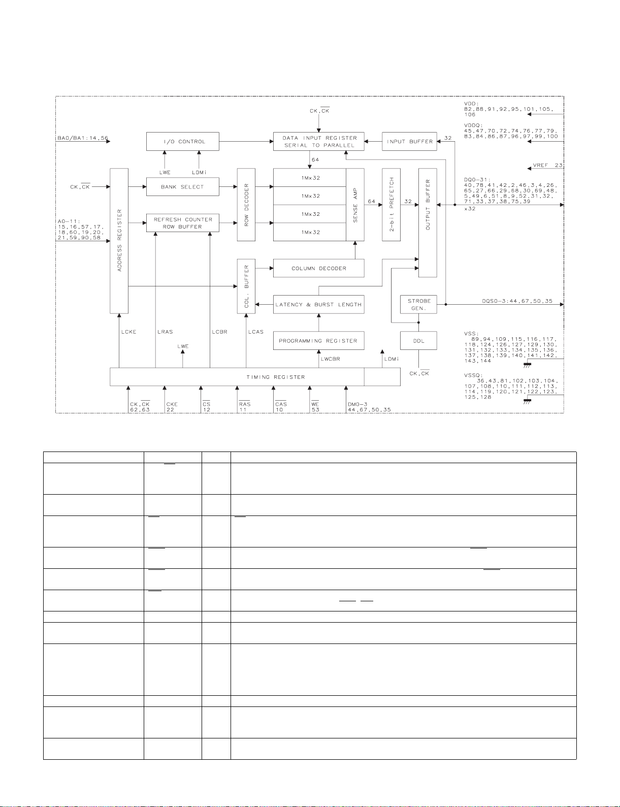
LC65RX1M
2.10. IC3501-2 (RH-iXC163WJQZQ)
2.10.1 Block Diagram
2.10.2 Pin Connections and short description
Pin No. Pin Name I/O Pin Function
62, 63 CK, CK
22 CKE I Activates the CK signal when high and deactivates the CK signal when low. By deactivating
12 CS
11 RAS
10 CAS
53 WE
1, 28, 7, 34 DQS0-3 I/O Data input and output are synchronized with both edge of DQS.
44, 67, 50, 35 DM0-3 I Data In mask. Data In is masked by DM Latency=0 when DM is high in burst write. DM0 for
40, 78, 41, 42, 2, 46, 3, 4,
26, 65, 27, 66, 29, 68, 30,
69, 48, 5, 49, 6, 51, 8, 9,
52, 31, 32, 71, 33, 37, 38,
75, 39
14, 56 BA0, BA1 I Selects which bank is to be active.
15, 16, 57, 17, 18, 60, 19,
20, 21, 59, 90, 58
82, 88, 91, 92, 95, 101,
105, 106
DQ0-31 I/O Data inputs/Outputs are multiplexed on the same pins.
A0-11 I Row/Column addresses are multiplexed on the same pins.
VDD — Power for the input buffers and core logic.
I The differential system clock Input.
All of the inputs are sampled on the rising edge of the clock except DQ’s and DM’s that are
sampled on both edges of the DQS.
the clock, CKE low indicates the Power down mode or Self refresh mode.
ICS enables the command decoder when low and disabled the command decoder when high.
When the command decoder is disabled, new commands are ignored but previous operations
continue.
I Latches row addresses on the positive going edge of the CK with RAS low.
Enables row access & precharge.
I Latches column addresses on the positive going edge of the CK with CAS low.
Enables column access.
I Enables write operation and row precharge.
Latches data in starting from CAS
DQ0 ~ DQ7, DM1 for DQ8 ~ DQ15, DM2 for DQ16 ~ DQ23, DM3 for DQ24 ~ DQ31.
Row addresses: RA0 ~ RA11, Column addresses: CA0 ~ CA7.
Column address CA8 is used for auto precharge.
, WE active.
7 – 17
Page 95

Pin No. Pin Name I/O Pin F unction
89, 94, 109, 115, 116,
117, 118, 124, 126, 127,
129, 130, 131, 132, 133,
134, 135, 136, 137, 138,
139, 140, 141, 142, 143,
144
45, 47, 70, 72, 74, 76, 77,
79, 83, 84, 86, 87, 96, 97,
99, 100
36, 43, 81, 102, 103, 104,
107, 108, 110, 111, 112,
113, 114, 119, 120, 121,
122, 123, 125, 128
23 VREF — Reference voltage for inputs, used for SSTL interface.
93, 61 RFU1/RFU2 — Reserved for Future Use.
13, 24, 25, 54, 55, 64, 73,
80, 85, 98
VSS — Ground for the input buffers and core logic.
VDDQ — Isolated power supply for the output buffers to provide improved noise immunity.
VSSQ — Isolated ground for the output buffers to provide improved noise immunity.
NC — No Connection.
2.11. IC8101 (RH-iXC011WJQZQ)
2.11.1 Pin Connections and short description
Ref No. Pin Name I/O Pin Function
DAC Interface
AD2 VDDZ_DAC — Digital power for DAC (+3.3V).
AD3 VSSZ_DAC — Digital ground for DAC.
AD1 DAC_VS I/O DAC vsync.
AE1 DAC_HS I/O DAC hsync.
AE2 DAC_CLK I/O DAC clock
AE4 DAC_DE I/O DAC DE
AE3 DAC_FLD I/O DAC field.
AA5 AVSS51 — Analog ground for DAC (for bias circuit).
AB5 COMP — Bias for DAC coupling capacitor.
AB4 IRSET I Bias for DAC current source.
AB3 CVBS_B I DAC blue or PB (Not used).
AB2 ADVSS2 — Analog ground for DAC (for DAC’s AVSS52).
AB1 ADVDD2 — Analog power for DAC (+3.3V).
AC1 C_G I DAC green or Y (Not used).
AC2 AVSS50 — Digital ground for DAC.
AC3 AVDD50 — Analog power for DAC (+3.3V).
AC4 Y_R I DAC red or PR (Not used).
AC5 ADVSS2 — Analog ground for DAC (for DAC’s AVSS52).
AD5 ADVDD2 — Analog power for DAC (+3.3V).
AD4 VM I DAC VM
ADC Interface
N2 AVDD — ADC power +3.3V.
N3 VIN1 I VRADC INPUT1 (Not used)
N4 VIN2 I VRADC INPUT2 (Not used)
N5 AVSS — ADC ground.
USB Interface
R3 USB_PPON_PP O USB Power on control.
R2 USB_OC_PP I USB over current control.
P5 VDDA — Analog core +3.3V supply.
P4 DN O Negative output channel.
P3 DP O Positive output control.
P2 VSSA — Analog core ground.
P1 RREFEXT — External resistor connection for current reference.
R5 VSSP — PLL ground pin Double Bond.
R4 VDDP — PLL +1.2V supply Double Bond.
LVDS Interface
AJ5 LVDS_VSSP — LVDS PLL Ground.
AJ3 LVDS_VDDP — LVDS PLL Power supply (+3.3V).
AK5 LVDS_VSSO — LVDS Output buffer VSS (Long pad)
AK4 LVDS_VDDO — LVDS Output buffer VDD (+3.3V).
AK1 TF2P O LVDS Positive Output. (Not used)
AK2 TF2M O LVDS Negative Output. (Not used)
LC65RX1M
7 – 18
Page 96

LC65RX1M
Ref No. Pin Name I/O Pin Function
AL1 TE2P O LVDS Positive Output. (Not used)
AL2 TE2M O LVDS Negative Output. (Not used)
AM1 TD2P O LVDS Positive Output. (Not used)
AM2 TD2M O LVDS Negative Output. (Not used)
AN1 TCLK2P O LVDS Positive clock Output. (Not used)
AN2 TCLK2M O LVDS Negative clock Output. (Not used)
AP1 TC2P O LVDS Positive Output. (Not used)
AP2 TC2M O LVDS Negative Output. (Not used)
AM4 LVDS_VDDO — LVDS Output buffer VDD (+3.3V).
AP3 TB2P O LVDS Positive Output. (Not used)
AN3 TB2M O LVDS Negative Output. (Not used)
AP4 TA2P O LVDS Positive Output. (Not used)
AN4 TA2M O LVDS Negative Output. (Not used)
AJ6 LVDS_VSSO — LVDS Output buffer VSS.
AP5 TF1P O LVDS Positive Output. (Not used)
AN5 TF1M O LVDS Negative Output. (Not used)
AP6 TE1P O LVDS Positive Output. (Not used)
AN6 TE1M O LVDS Negative Output. (Not used)
AP7 TD1P O LVDS Positive Output. (Not used)
AN7 TD1M O LVDS Negative Output. (Not used)
AP8 TCLK1P O LVDS Positive clock Output. (Not used)
AN8 TCLK1M O LVDS Negative clock Output. (Not used)
AP9 TC1P O LVDS Positive Output. (Not used)
AN9 TC1M O LVDS Negative Output. (Not used)
AJ4 LVDS_VDDO — LVDS Output buffer VDD (+3.3V).
AP10 TB1P O LVDS Positive Output. (Not used)
AN10 TB1M O LVDS Negative Output. (Not used)
AP11 TA1P O LVDS Positive Output. (Not used)
AN11 TA1M O LVDS Negative Output. (Not used)
AL5 LVDS_VSSO — LVDS Output buffer VSS.
AM5 LVDS_VDDO — LVDS Output buffer VDD (+3.3V).
AL3 LVDS_VSSA — LVDS Analog VSS.
AL4 LVDS_VDDA — LVDS Analog VDD (+3.3V).
AK3 LVDS_VSSD — LVDS Digital VSS.
AM3 LVDS_VDDD — LVDS Digital VDD (+3.3V).
PLL Interface
B7 DVSS22 — PLL ground related to DVDD22; supply for VCO circuit.
A7 DVDD22 — PLL power= 1.2V; supply for VCO circuit.
A6 DVSS21 — PLL ground related to DVDD21; supply for digital circuit.
B6 DVDD21 — PLL power= 1.2V; supply for digital circuit.
C6 AVSS7 — PLL ground related to AVDD7.
D6 MCLK2LF — Low pass filter for MCLK2PLL.
E6 AVDD7 — PLL analog power= 3.3V; supply for MCLK2PLL.
D5 AVSS6 — PL L ground related to AVSS6.
C5 MPEGCLK2LF — Low pass filter for MPEGCLK2PLL.
B5 AVDD6 — PLL analog power= 3.3V; supply for MPEGCLK2PLL.
A5 AVSS5 — PLL ground related to AVSS5.
A4 MPEGCLK1LF — Low pass filter for MPEGCLK1PLL.
B4 AVDD5 — PLL analog power= 3.3V; supply for MPEGCLK1PLL.
C4 AVSS2 — PL L ground related to AVSS2.
D4 PLF — Low pass filter for PCLKPLL.
C3 AVDD2 — PLL analog power= 3.3V; supply for PCLKPLL.
B3 AVSS1 — PLL ground related to AVSS1.
A3 MLF — Low pass filter for MCLKPLL.
A2 AVDD1 — PLL analog power= 3.3V; supply for MCLKPLL.
B2 AVSS4 — PLL ground related to AVSS4.
A1 IDELF — Low pass filter for IDECLKPLL.
B1 AVDD4 — PLL analog power= 3.3V; supply for IDECLKPLL.
C1 AVDD3 — PLL analog power= 3.3V; supply for CK48MPLL.
C2 CK48MLF — Low pass filter for CK48MPLL.
D3 AVSS3 — PL L ground related to AVSS3.
D2 XTLI — 24MHz_PLL crystal input.
D1 XTLO — 24MHz_PLL crystal output.
E1 DVSS12 — PLL ground related to DVDD12; supply for VCO circuit.
7 – 19
Page 97

LC65RX1M
Ref No. Pin Name I/O Pin Function
E2 DVDD12 — PLL power= 1.2V; supply for VCO circuit.
E3 DVSS11 — PLL ground related to DVDD11; supply for digital circuit.
E4 DVDD11 — PLL power= 1.2V; supply for digital circuit.
FLASH Interface
E25 AD30_FRA14 I/O Flash address 14/PCI AD bus bit 30.
D24 AD28_FRA12 I/O Flash address 12/PCI AD bus bit 28.
E24 AD26_FRA10 I/O Flash address 10/PCI AD bus bit 26.
A23 AD29_FRA13 I/O Flash address 13/PCI AD bus bit 29.
B23 AD31_FRA15 I/O Flash address 15/PCI AD bus bit 31.
D23 AD24_FRA8 I/O Flash address 8/PCI AD bus bit 24.
E23 AD22_FRA6 I/O Flash address 6/PCI AD bus bit 22.
A22 CBE3#_FRA19 I/O Flash address 19/PCI CBE#[3].
B22 AD25_FRA9 I/O Flash address 9/PCI AD bus bit 25.
C22 AD27_FRA11 I/O Flash address 11/PCI AD bus bit 27.
D22 AD20_FRA4 O Flash address 4/PCI AD bus bit 20/POD host interface Card access register selec-
E22 AD18_FRA2 O Flash address 2/PCI AD bus bit 18/POD host interface Card I/O output enable.
A21 AD19_FRA3 O Flash address 3/PCI AD bus bit 19/POD host interface Card I/O Write enable.
B21 AD21_FRA5 O Flash address 5/PCI AD bus bit 21.
C21 AD23_FRA7 O Flash address 7/PCI AD bus bit 23.
D21 AD16_FRA0 O Flash address 0/PCI AD bus bit 16/POD host interface Card I/O output enable.
A20 IRDY_PCAS I/O PCI bus IRDY# signal/M68K CPU interface address strobe signal.
B20 CBE2#_FRA18 O Flash address 18/PCI CBE#[2].
C20 AD17_FRA1 O Flash address 1/PCI AD bus bit 17/POD host interface Card I/O Write enable.
A19 CBE1#_FRA17 O Flash address 17/PCI CBE#[1].
E19 AD15_FRD15 I/O Flash Data bus bit 15/PCI AD bus bit 15.
A18 AD7_FRD7 I/O Flash Data bus 7/PCI AD bus bit 7.
B18 AD10_FRD10 I/O Flash Data bus bit 10/PCI AD bus bit 10/POD host interface address bit 2.
C18 AD12_FRD12 I/O Flash Data bus bit 12/PCI AD bus bit 12/POD host interface address bit 10.
D18 AD13_FRD13 I/O Flash Data bus bit 13/PCI AD bus bit 13/POD host interface address bit 13.
E18 AD11_FRD11 I/O Flash Data bus bit 11/PCI AD bus bit 11/POD host interface address bit 3.
A17 AD8_FRD8 I/O Flash Data bus bit 8/PCI AD bus bit 8/POD host interface address bit 0.
B17 AD14_FRD14 I/O Flash Data bus bit 14/PCI AD bus bit 14/POD host interface address bit 12.
C17 AD9_FRD9 I/O Flash Data bus bit 9/PCI AD bus bit 9/POD host interface address bit 1.
D17 AD6_FRD6 I/O Flash Data bus bit 6/PCI AD bus bit 6/POD host interface Data bus bit 6.
E17 CBE0#_FRA16 O Flash address 16/PCI CBE#[0].
A16 AD5_FRD5 O Flash Data bus bit 5/PCI AD bus bit 5/POD host interface Data bus bit 5.
B16 AD1_FRD1 I/O Flash Data bus bit 1/PCI AD bus bit 1/POD host interface Data bus bit 1.
C16 AD3_FRD3 I/O Flash Data bus bit 3/PCI AD bus bit 3/POD host interface Data bus bit 3.
D16 AD2_FRD2 I/O Flash Data bus bit 2/PCI AD bus bit 2/POD host interface Data bus bit 2.
E16 AD4_FRD4 I/O Flash Data bus bit 4/PCI AD bus bit 4/POD host interface Data bus bit 4.
E15 AD0_FRD0 I/O Flash Data bus bit 0/PCI AD bus bit 0/POD host interface Data bus bit 0.
D15 FRA25 I/O Flash address bit 25.
C15 FRA24 I/O Flash address bit 24.
B15 FRA23 I/O Flash address bit 23.
A15 FRA22 I/O Flash address bit 22.
A14 FRA21 I/O Flash address bit 21.
B14 FRA20 I/O Flash address bit 20.
C14 GCS3 I/O Flash chip select (0:Active).
D14 GCS2 I/O Flash chip select (0:Active).
E14 GCS1 I/O Flash chip select (0:Active).
E13 GCS0 I/O Flash chip select (0:Active).
D13 BOOTCS O EPPROM chip select (0:Active).
C13 FWE# O Write enable signal of Flash Rom.
B13 FOE# O Read enable signal of Flash Rom.
A13 NAND_CE# O Chip select signal of NAND Flash Rom.
A12 NAND_RDY I Ready signal of NAND Flash Rom.
PCI Interface
A27 INTA I PCI interrupt A.
C25 INTB I PCI interrupt B.
B27 INTC I PCI interrupt C.
B25 INTD I PCI interrupt D.
D27 GNT0 O PCI gnt signal. (Not used)
D26 GNT1 O PCI gnt signal. (Not used)
E26 GNT2 O PCI gnt signal. (Not used)
tion.
7 – 20
Page 98

LC65RX1M
Ref No. Pin Name I/O Pin Function
D25 GNT3 O PCI gnt signal. (Not used)
C27 PCIRST# O PCIRSTN/68K clock output.
A25 PCICLK O PCI clock.
C24 REQ0 I PCI req signal.
B24 REQ1 I PCI req signal.
A24 REQ2 I PCI req signal.
C23 REQ3 I PCI req signal.
E21 FRAME#_SIZI I/O PCI bus FRAME# signal/68K Transfer size bit 1. (analog with Transfer size bit 0 to
indicate the number byte to be transferred during a bus cycle M68K CPU bus.)
A20 IRDY_PCAS I/O PCI bus IRDY# signal/68K address strobe signal.
B20 CBE2#_FRA18 I/O PCI bus CBE#[2]/Flash address bit 18.
D20 TRDY#_SIZ0 I/O PCI bus TRDY# signal/68K Transfer size bit 0.
B19 SEPR#_DSACK1 I/O PCI bus SERR# signal/68K Data and Size acknowledge signal bit 1.
C19 DVSEL_PCDS I/O PCI bus DEVSEL# signal/68K Data Strobe signal.
D19 PAR_DSACK0 I/O PCI bus PAR signal/68K Data and Size acknowledge signal bit 0.
E20 STOP#_PCRW I/O Flash, 3.3V CMOS IF, 16mA output pad.
POD Interface
B12 POD_ITX I POD OOB TXI Channel.
C12 POD_WAIT I POD WAIT# signal to expand bus cycle.
D12 POD_CE1 O Card enable.
E12 POD_CTX O POD OOB TX Gapped Symbol clock.
A11 POD_DRX O POD OOB RX data.
B11 POD_CD1 I Card Detect.
C11 POD_IREQ I Ready/IRQ
D11 POD_CRX O POD OOB RX Gapped clock.
E11 POD_RESET O POD Card reset signal.
A10 POD_QTX I POD OOB TX Q Channel.
B10 POD_VS1 I Card voltage Sense.
C10 POD_ETX I POD OOB TX enable.
D10 POD_CD2 I Card Detect.
E10 POD_CE2 O Card enable.
A9 POD_VPP_EN O Slot VPP enable.
B9 POD_OVERLOAD I Current overload detect.
C9 POD_VPP_EN# O Slot VPP enable.
D9 POD_VCC_EN# O Slot VCC enable.
E9 POD_VCC_EN O Slot VCC enable.
A8 POD_A9 O POD Host interface address bit 9.
B8 POD_A8 O POD Host interface address bit 8.
C8 POD_A7 I/O POD Host interface address bit 7.
D8 POD_A6 I/O POD Host interface address bit 6.
D7 POD_A5 I/O POD Host interface address bit 5.
C7 POD_A4 O POD Host interface address bit 4.
VDA Interface
AP13, AN13, AM13, AL13,
AK13, AP14, AN14, AM14,
AL14, AK14
AP15, AN15, AM15, AL15,
AK15, AM16, AL16, AK16,
AP17, AN17
AM17, AL17, AK17, AP18,
AN18, AM18, AL18, AK18,
AP19, AN19
AP16 VDA_CLK I Video input, Clock. (Not used)
AM19 VDA_VS I Video input, Vertical sync. (Not used)
AL19 VDA_HS I Video input, Horizontal sync. (Not used)
AK19 VDA_DE I Video input, Data enable. (Not used)
VDB Interface, EJTAG, IDE and POD2 share with VDB
AK20 VDB_DE I/O Video input/output; data enable;
AL20 VDB_HS I/O Video input/output; Horizontal sync;
VDA_R[9:0] I Video input, R channel. (Not used)
VDA_B[9:0] I Video input, B channel. (Not used)
VDA_G[9:0] I Video input, G channel. (Not used)
IDE: IDE bus interrupt.
EJTAG: NOP
POD2: POD_CE2B#, the second POD Card enable.
IDE: PDLAGCBLID, Passed diagnostics, cable assembly type identifier.
EJTAG: TDI2, TDI EJTAG input of slave CPU.
POD2: POD_A_B5, the second POD host interface address bit 5.
7 – 21
Page 99

Ref No. Pin Name I/O Pin Function
AM20 VDB_VS I/O Video input/output; Vertical sync;
IDE: DMAREQ, IDE bus DMA request.
EJTAG: NOP
POD2: POD_A_B4, the second POD host interface address bit 4.
AN20 VDB_G0 I/O Video input/output; Green channel bit 0;
IDE: IDE data bus bit 0.
EJTAG: TDO2, TDO EJTAG input of slave CPU CPU.
POD2: POD_A_B6, the second POD host interface address bit 6.
AP20 VDB_G1 I/O Video input/output; Green channel bit 1;
IDE: IDE data bus bit 1.
EJTAG: TMS2, TMS EJTAG input of slave CPU CPU.
POD2: POD_A_B7, the second POD host interface address bit 7.
AK21 VDB_G2 I/O Video input/output; Green channel bit 2;
IDE: IDE data bus bit 2.
EJTAG: TCK2, TCK EJTAG input of slave CPU CPU.
POD2: POD_A_B8, the second POD host interface address bit 8.
AL21 VDB_G3 I/O Video input/output; Green channel bit 3;
IDE: IDE data bus bit 3.
EJTAG: DCLK EJTAG output of both CPU CPUs.
POD2: POD_A_B8, the second POD host interface address bit 9.
AM21 VDB_G4 I/O Video input/output; Green channel bit 4;
IDE: IDE data bus bit 4.
EJTAG: TPC[0], output as EJTAG PC Trace bus, bit 0.
POD2: POD_CD2B#, the second POD interface card detect.
AN21 VDB_G5 I/O Video input/output; Green channel bit 5;
IDE: IDE data bus bit 5.
EJTAG: TPC[1], output as EJTAG PC Trace bus, bit 1.
POD2: POD_CD1B#, the second POD interface card detect.
AP21 VDB_G6 I/O Video input/output; Green channel bit 6;
IDE: IDE data bus bit 6.
EJTAG: TPC[2], output as EJTAG PC Trace bus, bit 2.
POD2: POD_RSTB, the second POD host interface reset.
AK22 VDB_G7 I/O Video input/output; Green channel bit 7;
IDE: IDE data bus bit 7.
EJTAG: TPC[3], output as EJTAG PC Trace bus, bit 3.
POD3: POD_A_B14, the second POD host interface address bit 14.
AL22 VDB_G8 I/O Video input/output; Green channel bit 8;
IDE: IDE data bus bit 8.
EJTAG: TPC[4], output as EJTAG PC Trace bus, bit 4.
POD3: POD2_TS2_D0, the second POD_TS2 data[0].
AM22 VDB_G9 I/O Video input/output; Green channel bit 9;
IDE: IDE data bus bit 9.
EJTAG: TPC[5], output as EJTAG PC Trace bus, bit 5.
POD3: POD2_TS2_D2, the second POD_TS2 data[1].
AN22 VDB_B0 I/O Video input/output; Blue channel bit 0;
IDE: IDE data bus bit 10.
EJTAG: TPC[6], output as EJTAG PC Trace bus, bit 6.
POD3: POD2_TS2_D2, the second POD_TS2 data[2].
AP22 VDB_B1 I/O Video input/output; Blue channel bit 1;
IDE: IDE data bus bit 11.
EJTAG: TPC[7], output as EJTAG PC Trace bus, bit 7.
POD3: POD2_TS2_D3, the second POD_TS2 data[3].
AK23 VDB_B2 I/O Video input/output; Blue channel bit 2;
IDE: IDE data bus bit 12.
EJTAG: PCST[0], output as EJTAG PC Trace bus, bit 0.
POD3: POD2_TS2_D4, the second POD_TS2 data[4].
AL23 VDB_B3 I/O Video input/output; Blue channel bit 3;
IDE: IDE data bus bit 13.
EJTAG: PCST[1], output as EJTAG PC Trace bus, bit 1.
POD3: POD2_TS2_D5, the second POD_TS2 data[5].
AM23 VDB_B4 I/O Video input/output; Blue channel bit 4;
IDE: IDE data bus bit 14.
EJTAG: PCST[2], output as EJTAG PC Trace bus, bit 2.
POD3: POD2_TS2_D6, the second POD_TS2 data[6].
AP23 VDB_CLK I/O Video input/output; Clock;
IDE: IDE data bus IO access complete.
EJTAG: NOP
POD3: POD_CE1B#, the second POD interface card enable.
LC65RX1M
7 – 22
Page 100

LC65RX1M
Ref No. Pin Name I/O Pin Function
AK24 VDB_B5 I/O Video input/output; Blue channel bit 5;
AL24 VDB_B6 I/O Video input/output; Blue channel bit 6;
AM24 VDB_B7 I/O Video input/output; Blue channel bit 7;
AN24 VDB_B8 I/O Video input/output; Blue channel bit 8;
AP24 VDB_B9 I/O Video input/output; Blue channel bit 9;
AK25 VDB_R0 I/O Video input/output; Red channel bit 0;
AL25 VDB_R1 I/O Video input/output; Red channel bit 1;
AM25 VDB_R2 I/O Video input/output; Red channel bit 2;
AN25 VDB_R3 I/O Video input/output; Red channel bit 3;
AP25 VDB_R4 I/O Video input/output; Red channel bit 4;
AK26 VDB_R5 I/O Video input/output; Red channel bit 5;
AL26 VDB_R6 I/O Video input/output; Red channel bit 6;
AM26 VDB_R7 I/O Video input/output; Red channel bit 7;
AN26 VDB_R8 I/O Video input/output; Red channel bit 8;
AP26 VDB_R9 I/O Video input/output; Red channel bit 9;
IEEE1394 Interface, 8051 and 656 share with 1394
AM7, AL7, AK7, AK8, AL8,
AM8, AK9, AL9
HSD[7:0] I/O 1394: Parallel data.
IDE: IDE data bus bit 15.
EJTAG: PCST[3], output as EJTAG PC Trace bus, bit 3.
POD3: POD2_TS2_D7, the second POD_TS2 data[7].
IDE: Chip Select 0 for IDE interface.
EJTAG: PCST[4], output as EJTAG PC Trace bus, bit 4.
POD3: POD2_TS2_DEN, the second POD_TS2 data valid.
IDE: Chip Select 1 for IDE interface.
EJTAG: PCST[5], output as EJTAG PC Trace bus, bit 5.
POD2: POD2_TS2_CLK, the second POD_TS2 clock.
IDE: IDE address bus bit 0.
EJTAG: PCST[6], output as EJTAG PC Trace bus, bit 6.
POD2: POD2_TS2_SYNC, the second POD_TS2 SYNC.
IDE: IDE address bus bit 1.
EJTAG: PCST[7], output as EJTAG PC Trace bus, bit 7.
POD2: POD2_TS1_D0, the second POD_TS1 data[0].
IDE: IDE address bus bit 2.
EJTAG: PCST[8], output as EJTAG PC Trace bus, bit 8.
POD2: POD2_TS1_D1, the second POD_TS1 data[1].
IDE: IDE bus DMA acknowledge.
EJTAG: PCST[9], output as EJTAG PC Trace bus, bit 9.
POD2: POD2_TS1_D2, the second POD_TS1 data[2].
IDE: IDE bus IO Read Strobe signal.
EJTAG: PCST[10], output as EJTAG PC Trace bus, bit 10.
POD2: POD2_TS1_D3, the second POD_TS1 data[3].
IDE: IDE bus IO Write Strobe signal.
EJTAG: PCST[11], output as EJTAG PC Trace bus, bit 11.
POD2: POD2_TS1_D4, the second POD_TS1 data[4].
IDE: NOP
EJTAG:
S1=0, select DCLK/TPC[7:0]/PCST[11:0] of host CPU as output.
S1=1, select DCLK/TPC[7:0]/PCST[11:0] of slave CPU as output.
POD2: POD2_TS1_D5, the second POD_TS1 data[5].
IDE: NOP
EJTAG:
S1=0, two EJTAG are separately used.
S1=1, two EJTAG are used in a daisy chain style.
POD2: POD2_TS1_D6, the second POD_TS1 data[6].
IDE: NOP
EJTAG: TDI1, TDI EJTAG input of host CPU CPU.
POD2: POD2_TS1_D7, the second POD_TS1 data[7].
IDE: NOP
EJTAG: TDO1, TDO EJTAG input of host CPU CPU.
POD2: POD2_TS1_DEN, the second POD_TS1 data valid.
IDE: NOP
EJTAG: TMS1, TMS EJTAG input of host CPU CPU.
POD2: POD2_TS1_CLK, the second POD_TS1 clock.
IDE: NOP
EJTAG: TCK1, TCK EJTAG input of host CPU CPU.
POD2: POD2_TS1_SYNC, the second POD_TS1 SYNC.
Video 656 port; 656D[9:2], data[9:2]
8051: AD[7:0], AD bus.
7 – 23
 Loading...