

Page 1
LC-39/50LE650
160mm
125mm
100mm
80mm
63mm
50mm
A-data-1
Corporate Trademark
LC-39/50LE651
LC-39/50LE652
SERVICE MANUAL
S1stLC39LE650
Issued: 14
th
June 2013
1st Edition
Wi-Fi & 3D Ready / DVB-T / T2 / C / S / S2 PAL B/G / SECAM B/G, D/K, L/L’ SYSTEM COLOUR TELEVISION
LED LCD COLOUR TELEVISION
MODELS
LC-39LE650E/RU/V
LC-39LE651E/K/RU/V
LC-39LE652E/RU/V
LC-50LE650E/RU/V
LC-50LE651E/K/RU/V
LC-50LE652E/RU/V
In the interests of user safety (required by safety
regulations in some countries) the set should be restored to its original condition and only parts identical
to those speci ed should be used.
CONTENTS
ELECTRICAL SPECIFICATIONS ........................................................................................ 2
IMPORTANT SERVICE SAFETY PRECAUTIONS ......................................................................... 3
OPERATION MANUAL .................................................................................................................... 6
DIMENSIONS .................................................................................................................... 22
REMOVING OF MAJOR PARTS ..................................................................................................... 23
SERVICE ADJUSTMENTS ............................................................................................................. 33
PUBLIC MODE .................................................................................................................................... 44
SOFTWARE UPGRADING ............................................................................................................. 47
MAJOR ICs INFORMATION ..................................................................................................... 48
BLOCK DIAGRAMS ..................................................................................................................... 63
SCHEMATIC DIAGRAMS ....................................................................................................... 66
PRINTED WIRING BOARDS ......................................................................................................... 114
REPLACEMENT PARTS LIST ....................................................................................................... 121
CABINET AND MECHANICAL PARTS ............................................................................................ 141
PACKING OF THE SET ....................................................................................................................... 145
SHARP CORPORATION
1
This document has been published to
be used for after sales service only.
The contents are subject to chage without notice.
Page 2

LC-39/50LE650
Appendix
LC-39/50LE651
LC-39/50LE652
Specifications
ELECTRICAL SPECIFICATIONS
Item
LCD Panel (
Resolution 6.220.800 dots (1.920 x 1.080 pixels)
Video Colour System PAL/SECAM/NTSC 3.58/NTSC 4.43/PAL 60
TV
Functions
Viewing angles H: 176°, V: 176°
Audio Ampli er 15 W + 15 W (Music power)
Speaker (96 mm x 30mm) x 2
Terminals
OSD language
Power Requirement AC 220–240 V, 50 Hz
Power Consumption (IEC62087 Method) 99W
Weight 10.7Kg
Operating Temperature 0 °C to +40 °C
LED TV) 39” BLACK TFT 50” BLACK TFT 60” BLACK TFT
TV Standard Analogue CCIR (B/G, I, D/K, L/L’)
Digital DVB-T (2K/8K OFDM)(H.264), DVB-C, DVB-C2 (L*654 only), DVB-T2(L*651/654
Receiving
Channel
TV-Tuning System Auto Preset 999 ch: non-Nordic / 9999 ch: Nordic (ATV: 99 ch), Auto Label, Auto Sort
STEREO / BILINGUAL NICAM/A2
TV Antenna VHF/UHF UHF/VHF 75 Ω Din type (Analogue & Digital)
SERVICE Ø 3.5 mm jack
SCART SCART (AV input, RGB input, TV output, Y/C input)
PC INPUT VGA (D-Sub 15pin), Ø 3.5 mm jack (shared with HDMI)
COMPONENTS COMPONENT IN: Y/PB(CB)/PR(CR), RCA (AUDIO R/L)
HDMI1 HDMI, Ø 3.5 mm jack (shared with PC INPUT), ARC, 3D.
HDMI2 HDMI, Ø 3.5 mm jack (shared with PC INPUT), 3D.
HDMI3 HDMI, Ø 3.5 mm jack (shared with PC INPUT), 3D.
HDMI4 HDMI, Ø 3.5 mm jack (shared with PC INPUT), 3D.
USB 1 USB 2.0 HOST (A Type)
USB 2 USB 2.0 HOST (A type)
USB 3 (WIFI) USB 2.0 HOST (A type) (Wi-Fi use only)
ETHERNET (10/100) Network connector
AV RCA connector (AV input)
S/PDIF OUT RCA S/PDIF digital audio output.
C. I. (Common Interface) EN50221, R206001, CI+ speci cation
Headphones Ø 3.5 mm jack (Audio output)
VHF/UHF E2–E69 ch, F2–F10 ch, I21–I69 ch, IR A–IR J ch (Digital: IR A ch–E69 ch)
CATV Hyper-band, S1–S41 ch
Satellite (652/654
series only)
39” LCD COLOUR TV,
Models:
LC-39LE650E/RU/V
LC-39LE651
LC-39LE652E/RU/V
LC-39LE654E/RU/V
LC-39LU651E
LC-39LM652E/V
LC-39LK652E
LC-39LX652E
only), DVB-S/S2 (L*652/654 only)
75 Ω F type (DVB-S/S2)
Czech, Danish, Dutch, English, Estonian, Finnish, French, German, Greek, Hungarian,
Italian, Latvian, Lithuanian, Norwegian, Polish, Portuguese, Russian, Slovak, Slovene,
Spanish, Swedish, Turkish, Ukrainian, Byelorussian, Romanian, Croatian, Serbian.
(0.24W Stby)
13.3 Kg (With stand)
E/K/RU/V
(Without stand)
50” LCD COLOUR TV,
Models:
LC-50LE650E/RU/V
LC-50LE651
LC-50LE652E/RU/V
LC-50LE654E/RU/V
LC-50LU651E
LC-50LM652E/V
LC-50LK652E
LC-50LX652E
121W
(0.24W Stby)
16.7Kg
20.1Kg (With stand)
E/K/RU/V
(Without stand)
60” LCD COLOUR TV,
Models:
LC-60LE650E/RU
LC-60LE651
LC-60LE652E/RU
LC-60LE654E/RU
LC-60LU651E
LC-60LM652E
LC-60LK652E
LC-60LX652E
175W
(0.24W Stby)
24.3Kg
29.6 Kg (With stand)
E/K/RU
(Without stand)
2
Page 3
LC-39/50LE650
LC-39/50LE651
LC-39/50LE652
IMPORTANT SERVICE SAFETY PRECAUTION
Service work should be performed only by qualied service technicians who are thoroughly familiar with all
safety checks and the servicing guidelines which follow:
WARNING
1. For continued safety, no modication of any circuit should be attempted.
2. Disconnect AC power before servicing.
CAUTION: FOR CONTINUED PROTECTION AGAINST A RISK OF
FIRE REPLACE ONLY WITH SAME TYPE F101 (T4 AH / 250V)
BEFORE RETURNING THE RECEIVER (Fire & Shock Hazard)
Before returning the receiver to the user, perform the following safety checks:
1. Inspect all lead dress to make certain that leads are not pinched, and check that hardware is not lodged between the
chassis and other metal parts in the receiver.
2. Inspect all protective devices such as non-metallic control knobs, insulation materials, cabinet backs, adjustment and
compartment covers or shields, isolation resistor-capacitor networks, mechanical insulators, etc.
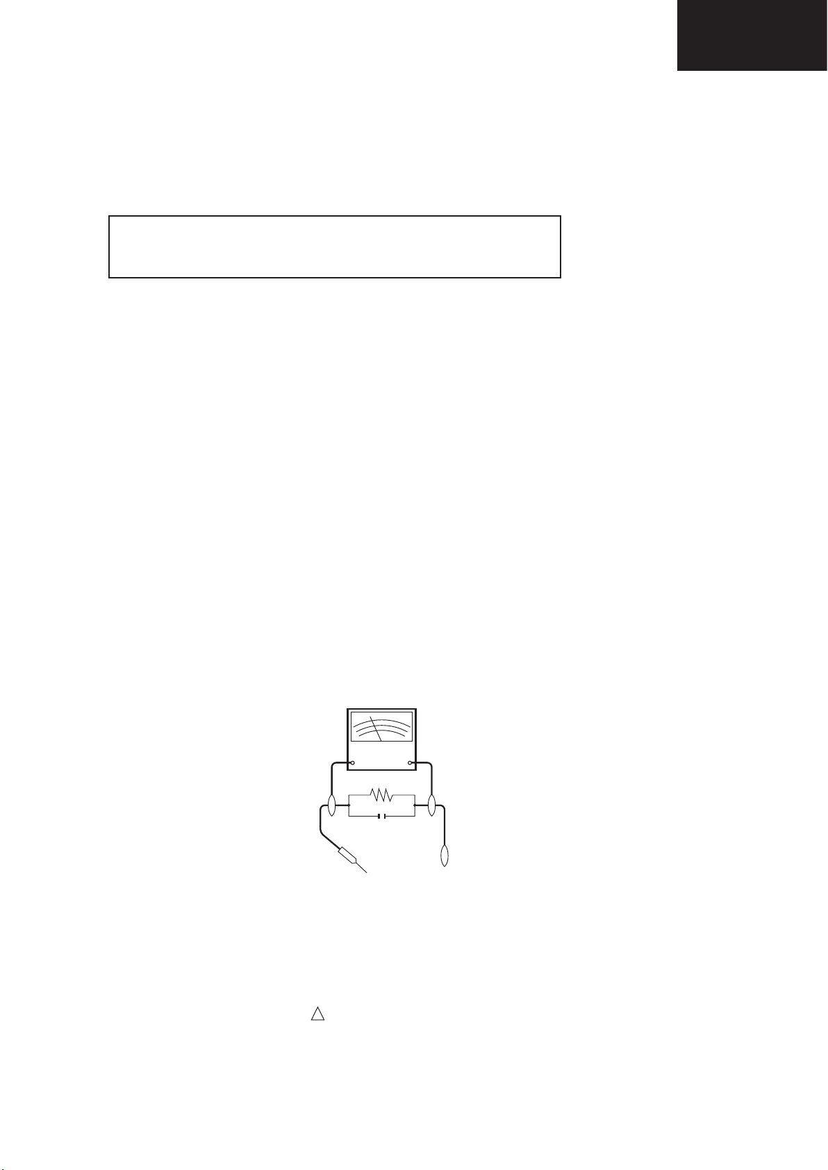
3. To be sure that no shock hazard exists, check for leakage current in the following manner.
• Plug the AC cord directly into a 220~240 volt AC outlet. (Do not use an isolation transformer for this test).
•Using two clip leads, connect a 1.5k ohm, 10 watt resistor paralleled by a 0.15µF capacitor in series with all exposed metal
cabinet parts and a known earth ground, such as electrical conduit or electrical ground connected to an earth ground.
•A true RMS reading multimeter should be used for this test, especially where the equipment uses a switch mode
power supply which may result in very non-sinusoidal leakage current.
•Connect the resistor connection to all exposed metal parts having a return to the chassis (antenna, metal cabinet,
screw heads, knobs and control shafts, escutcheon, etc.) and measure the AC voltage drop across the resistor.
All checks must be repeated with the AC cord plug connection reversed. (If necessary, a nonpolarized adaptor plug must
be used only for the purpose of completing these checks.)
Any reading of 1.05V peak (this corresponds to 0.7 mA. peak AC.) or more is excessive and indicates a potential shock
hazard which must be corrected before returning the monitor to the owner.
DVM
AC SCALE
1.5k ohm
10W
0.15 µF
TEST PROBE
TO EXPOSED
METAL PARTS
CONNECT TO
KNOWN EARTH
GROUND
SAFETY NOTICE
Many electrical and mechanical parts in LCD television have special safety-related characteristics.
These characteristics are often not evident from visual inspection, nor can protection afforded by them be necessarily
increased by using replacement components rated for higher voltage, wattage, etc.
Replacement parts which have these special safety characteristics are identied in this manual; electrical components
having such features are identied by “ “.
!
For continued protection, replacement parts must be identical to those used in the original circuit.
The use of a substitute replacement parts which do not have the same safety characteristics as the factory recommended
replacement parts shown in this service manual, may create shock, re or other hazards.
3
Page 4
LC-39/50LE650
L F a
LC-39/50LE651
LC-39/50LE652
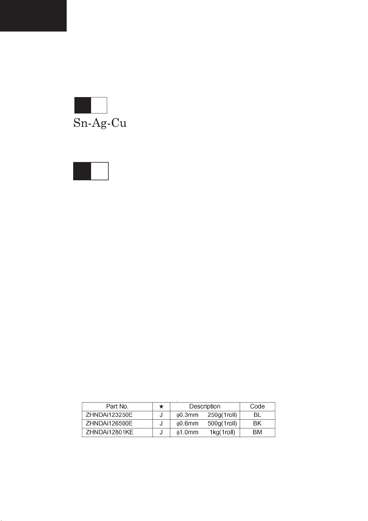
PRECAUTIONS FOR USING LEAD-FREE SOLDER
1 Employing lead-free solder
“ALL PWB” of this model employs lead-free solder. The LF symbol indicates lead-free solder, and is attached on the
PWBs and service manuals. The alphabetical character following LF shows the type of lead-free solder.
Example:
Indicates lead-free solder of tin, silver and copper.
L F n
Sn-Ag-Ni
Indicates lead-free solder of tin, silver and nickel.
2 Using lead-free wire solder
When xing the PWB soldered with the lead-free solder, apply lead-free wire solder. Repairing with conventional lead
wire solder may cause damage or accident due to cracks.
As the melting point of lead-free solder (Sn-Ag-Cu) is higher than the lead wire solder by 40°C, we recommend you to
use a dedicated soldering bit, if you are not familiar with how to obtain lead-free wire solder or soldering bit, contact our
service station or service branch in your area.
3 Soldering
As the melting point of lead-free solder (Sn-Ag-Cu) is about 220°C which is higher than the conventional lead solder by
40°C, and as it has poor solder wettability, you may be apt to keep the soldering bit in contact with the PWB for extended
period of time. However, Since the land may be peeled off or the maximum heat-resistance temperature of parts may be
exceeded, remove the bit from the PWB as soon as you conrm the steady soldering condition.
Lead-free solder contains more tin, and the end of the soldering bit may be easily corroded. Make sure to turn on and
off the power of the bit as required.
If a different type of solder stays on the tip of the soldering bit, it is alloyed with lead-free solder. Clean the bit after every
use of it.
When the tip of the soldering bit is blackened during use, le it with steel wool or ne sandpaper.
Be careful when replacing parts with polarity indication on the PWB silk.
Lead-free wire solder for servicing.
4
Page 5
END OF LIFE DISPOSAL
A. Information on Disposal for Users (private households)
1. In the European Union
Attention: If you want to dispose of this equipment, please do not use the ordinary dust bin!
Used electrical and electronic equipment must be treated separately and in accordance with legislation that requires
proper treatment, recovery and recycling of used electrical and electronic equipment.
Following the implementation by member states, private households within the EU states may return their used
electrical and electronic equipment to designated collection facilities free of charge*. In some countries* your local
retailer may also take back your old product free of charge if you purchase a similar new one.
*) Please contact your local authority for further details.
If your used electrical or electronic equipment has batteries or accumulators, please dispose of these separately
beforehand according to local requirements.
By disposing of this product correctly you will help ensure that the waste undergoes the necessary treatment, recovery
and recycling and thus prevent potential negative effects on the environment and human health which could otherwise
arise due to inappropriate waste handling.
2. In other Countries outside the EU
If you wish to discard this product, please contact your local authorities and ask for the correct method of disposal.
For Switzerland: Used electrical or electronic equipment can be returned free of charge to the dealer, even if you don’t
purchase a new product. Further collection facilities are listed on the homepage of www.swico.ch or www.sens.ch.
B. Information on Disposal for Business Users
1. In the European Union
If the product is used for business purposes and you want to discard it:
Please contact your SHARP dealer who will inform you about the take-back of the product. You might be charged for
the costs arising from take-back and recycling. Small products (and small amounts) might be taken back by your local
collection facilities.
For Spain: Please contact the established collection system or your local authority for take-back of your used
products.
2. In other Countries outside the EU
If you wish to discard of this product, please contact your local authorities and ask for the correct method of disposal.
Attention: Your product
is marked with this
symbol. It means that
used electrical and
electronic products
should not be mixed
with general household
waste. There is a
separate collection
system for these
products.
End of life disposal
The battery supplied with this product contains traces of Lead.
For EU: The crossed-out wheeled bin implies that used batteries should not be put to the general household waste!
There is a separate collection system for used batteries, to allow proper treatment and recycling in accordance with
legislation. Please contact your local authority for details on the collection and recycling schemes.
For Switzerland: The used battery is to be returned to the selling point.
For other non-EU countries: Please contact your local authority for correct method of disposal of the used battery.
LC-39/50LE650
LC-39/50LE651
LC-39/50LE652
5
Page 6
LC-39/50LE650
Introduction
LC-39/50LE651
LC-39/50LE652
Remote control unit
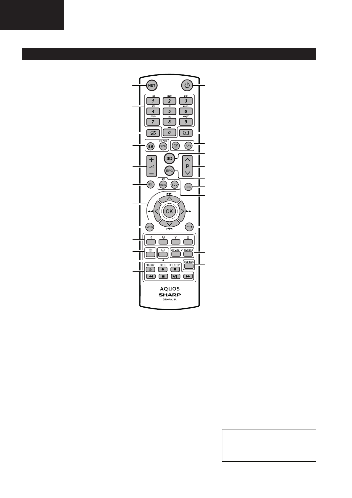
OPERATION MANUAL
1 NET (Page 37)
Access “AQUOS NET+” mode.
2 Alphanumeric buttons 0_9
Set the channel. Enter desired
numbers. Set the page in teletext
mode.
• When the five Nordic countries
(Sweden, Norway, Finland,
Denmark or Iceland) are selected
in the country setting from initial
auto installation (Page 9), DTV
services are four digits. When
another country is selected, DTV
services are three digits.
3 A (Flashback)
Return to the previously selected
channel or external input.
4 7 (Sound mode) (Page17)
Select a sound multiplex mode.
f Picture format (Page 31)
Change between different picture
formats.
5 i+/- (Volume)
Increase/decrease TV volume.
6 e (Mute)
TV sound on/off.
7 a/b/c/d (Cursor)
Select a desired item.
;
Execute a command.
ATV/DTV/SAT: Display “CH list” when
no other “MENU” screen is running.
T/S/V/U
Not used.
8 @
Main menu screen on.
Come back to last option selected
within MENU screen.
9 R/G/Y/B Colour buttons
The coloured buttons are
correspondingly used to select the
coloured items on the screen (e.g.,
EPG, MHEG-5, teletext).
10 m Teletext (Page 20)
ATV: Display analogue teletext.
DTV/SAT: Select MHEG-5 or teletext
for DTV/SAT.
11 [ Subtitle (Pages 17 and 20)
Switch subtitle languages on/off.
1
23
2
3
4
22
21
20
5
19
18
6
17
16
7
8
15
9
10
11
14
13
12
12 S/I/J/E/H (Pages 49 and
53)
Video/Music/USB REC files
reproduction buttons.
a SOURCE (Page 44)
Operating HDMI-CEC device.
13 USB REC (
Record a programme you are
watching.
Page 49)
14 ATV/DTV
Access TV mode.
RADIO
DTV/SAT: Switch between radio and
data mode.
• When only data broadcasting
(no radio broadcasting) is
transmitted by DVB, the radio
broadcasting will be skipped.
15 6 Back
ATV/DTV/SAT: Return to the previous
“Menu” screen.
NET: Return to the previous page
(This may not function for some
services).
16 Picture adjustment (Page 21)
Select picture settings.
ECO (Page 21)
Activate/deactivate low consumption
mode (ECO).
17 >
ATV/DTV/SAT: Exit the “Menu”
screen.
18 EPG (Page 18)
DTV/SAT: Display the EPG screen.
19 :r/s
ATV/DTV/SAT: Select the TV
channel.
NET: Scrolls pages up/down.
20 3D (Page 54)
Select between 3D and 2D image
viewing.
21 p Channel information (Page 15)
Display the station information
(channel number, signal, etc.) on the
screen.
Within MENU screen shows a hint
about item selected.
FAV
Define active station as favourite.
22 b (AV selection) (Page 17)
Select an input source.
23 a (Standby/On) (Page 17)
Important information:
Satellite services are only
available for the LE652/654
model series.
6
Page 7
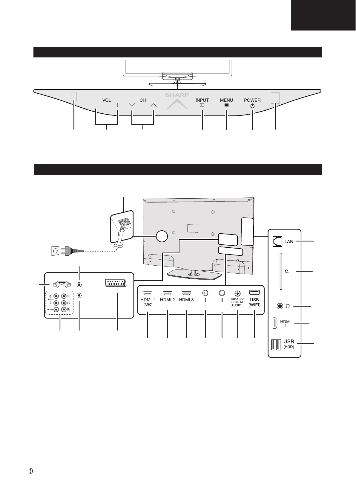
Operation Manual (Continued)
Introduction
4
TV (Front view)
*TV indicator status (Page 17)
TV (Side and rear view)
Remote
Control
Sensor
Volume
buttons
Illumination led*
Programme (channel)
buttons
Input
source
button
Menu
button
Power
button
LC-39/50LE650
LC-39/50LE651
LC-39/50LE652
3D infrared
emitter
18
17
1
16
PC IN
2
3
4
HDMI/PC
ANALOG
AUDIO
INPUT
SERVICE
SCART (AV / RGB / S-VIDEO)
5
ANT
SAT
6
7 8
10
9
12
11
15
14
13
1 Analog AUDIO input for DVI and PC
(Jack 3.5mm connector)
2 PC Input
3 COMPONENTS / AV terminals
4 SERVICE connector (jack 3.5 mm)
5 SCART (AV/RGB, Y/C Input) terminal
6 HDMI 1 (HDMI/DVI/ARC)
7 HDMI 2 (HDMI/DVI)
8 HDMI 3 (HDMI/DVI)
9 Antenna input terminal
10 SAT (Satellite antenna input) (Only
L*652 series)
11 Digital Audio Output terminal (SPDIF)
12 USB terminal (Wi-Fi use only)
13 USB terminal (USB REC / MEDIA
PLAYER / SOFTWARE / HDD READY
/ 3D GLASSES BATTERY)
14 HDMI 4 (HDMI/DVI)
15 HEADPHONES jack
16 COMMON INTERFACE slot
17 LAN terminal
18 AC INPUT terminal
WARNING
• Excessive sound pressure from earphones and headphones can cause hearing loss.
• Do not set the volume at a high level. Hearing experts advise against extended listening at high volume levels.
7
Page 8
LC-39/50LE650
Preparation
LC-39/50LE651
LC-39/50LE652
Operation Manual (Continued)
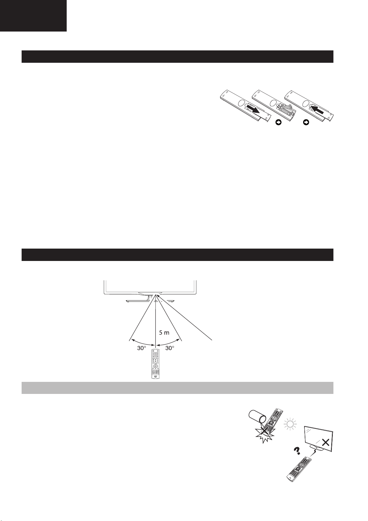
Inserting the batteries
Before using the TV for the first time, insert the two supplied “AAA” size batteries. When the batteries become
depleted and the remote control unit fails to operate, replace the batteries with new “AAA” size batteries.
1 Open battery cover.
2 Insert two supplied “AAA” size batteries.
• Place batteries with their terminals corresponding to
the (+) and (-) indicators in the battery compartment.
3 Close the battery cover.
CAUTION
Improper use of batteries can result in chemical leakage or explosion. Be sure to follow the instructions below.
• Do not mix batteries of different types. Different types of batteries have different characteristics.
• Do not mix old and new batteries. Mixing old and new batteries can shorten the life of new batteries or cause
chemical leakage in old batteries.
• Remove batteries as soon as they have worn out. Chemicals that leak from batteries can cause a rash. If you fi nd
any chemical leakage, wipe thoroughly with a cloth.
• The batteries supplied with this product may have a shorter life expectancy due to storage conditions.
• If you will not be using the remote control unit for an extended period of time, remove the batteries from it.
• When replacing the batteries, use zinc-carbon batteries instead of alkaline ones.
Note on disposing batteries:
The batteries provided contain no harmful materials such as cadmium, lead or mercury.
Regulations concerning used batteries stipulate that batteries may no longer be thrown out with the household
rubbish. Deposit any used batteries free of charge into the designated collection containers set up at commercial
businesses.
Using the remote control unit
Use the remote control unit by pointing it towards the remote control sensor. Objects between the remote control
unit and sensor may prevent proper operation.
Remote control sensor
Cautions regarding the remote control unit
• Do not expose the remote control unit to shock. In addition, do not expose the remote control unit to liquids,
and do not place in an area with high humidity.
• Do not install or place the remote control unit under direct sunlight. The heat
may cause deformation of the unit.
• The remote control unit may not work properly if the remote control sensor of
the TV is under direct sunlight or strong lighting. In such cases, change the
angle of the lighting or the TV, or operate the remote control unit closer to the
remote control sensor.
8
Page 9

Operation Manual (Continued)
Quick guide
Initial installation overview
LC-39/50LE650
LC-39/50LE651
LC-39/50LE652
Follow the steps below one by one when using the TV for the first time. Some steps may not be necessary
depending on your TV installation and connection.
1 2 3
Preparation
Connect an antenna cable to
the antenna terminal (Page 8).
If necessary, insert a CA
card into the CI slot to watch
scrambled broadcasts
(Page 8.)
Power on and
run the auto
installation
Turn on the power using a on
the TV (Page 17).
Run the initial auto installation
(Page 9).
Language, Energy
Efficiency, country, antenna
type settings, etc.
Watch TV
Congratulations!
Now you can watch TV.
If necessary, adjust the
antenna to attain maximum
signal reception (Page 14).
Connect
external devices
Connect external
devices such as a
DVD player/recorder
as instructed (Pages
41, 42 and 43).
Plug in the AC cord (Page 8).
Product shape varies in some countries.
Go to Next.
Start searching
channels
9
Connect external
audio devices such as
speakers/amplifier as
instructed (Pages 41,
42 and 43).
Page 10
LC-39/50LE650
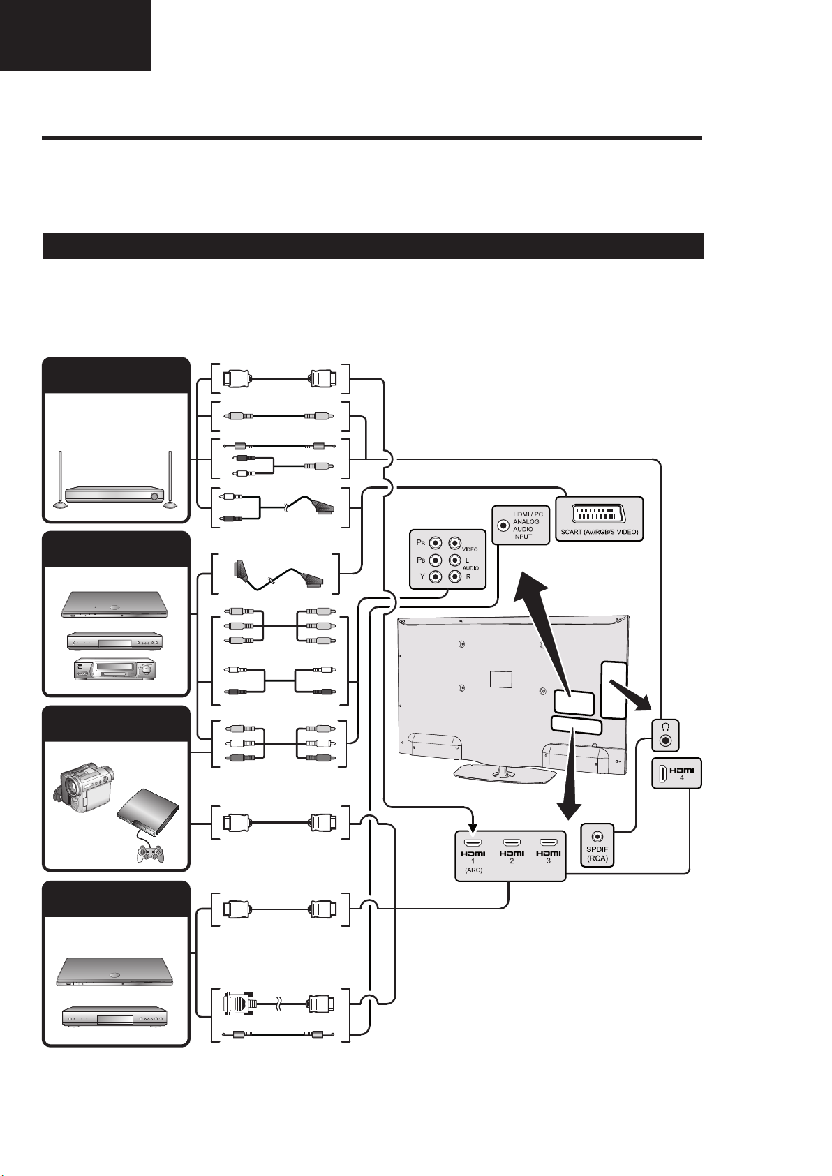
Connecting external devices
LC-39/50LE651
LC-39/50LE652
Operation Manual (Continued)
E Before connecting ...
• Be sure to turn off the TV and any devices before making any connections.
• Firmly connect a cable to a terminal or terminals.
• Carefully read the operation manual of each external device for possible connection types. This also helps you get
the best possible audiovisual quality to maximise the potential of the TV and the connected device.
Introduction to connections
The TV is equipped with the terminals as shown below. Find the cable corresponding the TV’s terminal and connect
the device.
NOTE
• The cables illustrated in pages 41, 42 and 43 are commercially available items.
Audio device
(Page 43)
Video recording device
(Pages 42 and 43)
Game console or
camcorder (Page 42)
HDMI-ARC
Audio cable
Audio cable
SCART cable
Components cable
Audio cable
AV cable
HDMI device
(Page 42)
HDMI-certified cable
HDMI-certified cable
DVI/HDMI Cable
ø 3.5 mm stereo mini jack cable
10
Page 11
Operation Manual (Continued)
Enjoying 3D image viewing
Display format for 3D and 2D images
Image for input signals Selectable mode Description
3D mode
(using the 3D
glasses)
2D→3D
• Converts normal 2D images into 3D images.
Side by Side
• Creates 3D images from 3D images displayed side
by side. The image is split into a left and right image,
and then the images are stretched and displayed
sequentially to create a 3D image.
Top and Bottom
• Creates 3D images from 3D images displayed
on the top and bottom. The image is split into a
top and bottom image, and then the images are
stretched and displayed sequentially to create a 3D
image.
2D mode
(without using
the 3D glasses)
Side by Side s 2D
• Creates 2D images from 3D images displayed
side by side. Only the left image is stretched and
displayed. The image does not appear in 3D.
Top and Bottom s 2D
• Creates 2D images from 3D images displayed on
the top and bottom. Only the top image is stretched
and displayed. The image does not appear in 3D.
Troubleshooting - 3D Images
NOTE
• These 3D glasses are only for use with SHARP LCD TVs supporting 3D.
Appendix
Troubleshooting
Problem Possible Solution
• No power.
• Check if you pressed
a
on the remote control unit.
If the indicator on the TV lights up red, press
a
.
• Is the AC cord disconnected?
• Check if you pressed a on the TV.
• The TV cannot be operated. • External influences such as lightning, static electricity, etc., may cause improper operation. In this
case, operate the TV after first turning off the power, or unplugging the AC cord and re-plugging
it in after one or two minutes.
• Remote control unit does not operate.
• Are batteries inserted with polarity (e, f) aligned?
• Are batteries worn out? (Replace with new batteries.)
• Are you using it under strong or fluorescent lighting?
• Is a fluorescent light illuminating the remote control sensor?
• Picture is cut off. • Is the image position correct?
• Are screen mode adjustments (Picture format) such as picture size made correctly? (Page 31.)
• Strange colour, light colour, or dark
colour, or colour misalignment.
• Adjust the picture tone.
• Is the room too bright? The picture may look dark in a room that is too bright.
• Check the “Picture” settings (Page 21).
• Power is suddenly turned off. • The TV’s internal temperature has increased.
Clean or remove any objects blocking the vent.
• No picture. • Are connections to external equipment correct? (Pages 41, 42 and 43)
• Is the input signal type selected correctly after connection? (Page 14)
• Is the correct input source selected? (Page 31)
• Is the picture adjustment correct? (Pages 21)
• Is the antenna connected properly? (Pages 7 and 14)
• No sound. • Is the volume too low?
• Make sure that headphones are not connected.
• Check if you pressed e on the remote control unit.
• The TV sometimes makes a cracking
sound.
• This is not a malfunction. This happens when the cabinet slightly expands and contracts
according to changes in temperature. This does not affect the TV’s performance.
Appendix
Troubleshooting
Problem Possible Solution
• No power.
• The TV cannot be operated. • External influences such as lightning, static electricity, etc., may cause improper operation. In this
• Remote control unit does not operate.
• Picture is cut off. • Is the image position correct?
• Strange colour, light colour, or dark
colour, or colour misalignment.
• Power is suddenly turned off. • The TV’s internal temperature has increased.
• No picture. • Are connections to external equipment correct? (Pages 41, 42 and 43)
• No sound. • Is the volume too low?
• The TV sometimes makes a cracking
sound.
Problem Possible solution
• 3D images are not displayed. • Is 3D mode set to “Automatic”? Press 3D to switch to 3D mode "Automatic".
• The 3D glasses turn off
automatically.
• Switching the 3D glasses button to
2D or 3D does not cause the LED
to light up green.
Information on the software license for this product
Software composition
• Check if you pressed
If the indicator on the TV lights up red, press
• Is the AC cord disconnected?
• Check if you pressed a on the TV.
case, operate the TV after first turning off the power, or unplugging the AC cord and re-plugging
it in after one or two minutes.
• Are batteries inserted with polarity (e, f) aligned?
• Are batteries worn out? (Replace with new batteries.)
• Are you using it under strong or fluorescent lighting?
• Is a fluorescent light illuminating the remote control sensor?
• Are screen mode adjustments (Picture format) such as picture size made correctly? (Page 31.)
• Adjust the picture tone.
• Is the room too bright? The picture may look dark in a room that is too bright.
• Check the “Picture” settings (Page 21).
Clean or remove any objects blocking the vent.
• Is the input signal type selected correctly after connection? (Page 14)
• Is the correct input source selected? (Page 31)
• Is the picture adjustment correct? (Pages 21)
• Is the antenna connected properly? (Pages 7 and 14)
• Make sure that headphones are not connected.
• Check if you pressed e on the remote control unit.
• This is not a malfunction. This happens when the cabinet slightly expands and contracts
according to changes in temperature. This does not affect the TV’s performance.
• If 3D mode is set to “Automatic” but no 3D images are displayed, check the display format of the
content being viewed. Some 3D image signals may not be recognised as 3D images automatically.
Press 3D to select the appropriate display format for the 3D image.
• Are the 3D glasses set to 3D mode?
• Is there an obstacle between the 3D glasses and the TV, or is something covering the infrared
receiver on the 3D glasses? The 3D glasses operate by receiving a signal from the TV. Do not place
anything between the 3D infrared emitter on the TV and the infrared receiver on the 3D glasses.
• Is there an obstacle between the 3D glasses and the TV, or is something covering the infrared
receiver on the 3D glasses? The 3D glasses turn off automatically after three minutes if no signal
is received from the TV. Do not place anything between the 3D infrared emitter on the TV and the
infrared receiver on the 3D glasses.
• Is the battery in the 3D glasses exhausted? If the LED light does not light after pressing the power
button for more than one second, the battery is exhausted. Recharge the battery via mini USB
connector.
The software included in this product is comprised of various software components whose individual copyrights are held by
SHARP or by third parties.
Software developed by SHARP and/or third part
The copyrights for the software components and various relevant documents included with this product that were developed or
written by SHARP are owned by SHARP and are protected by the Copyright Act, international treaties, and other relevant laws.
This product also makes use of freely distributed software and software components whose copyrights are held by third parties.
a
on the remote control unit.
a
.
LC-39/50LE650
LC-39/50LE651
LC-39/50LE652
11
Page 12
LC-39/50LE650
LC-39/50LE651
LC-39/50LE652
Operation Manual (Continued)
Multimedia/Network Setup
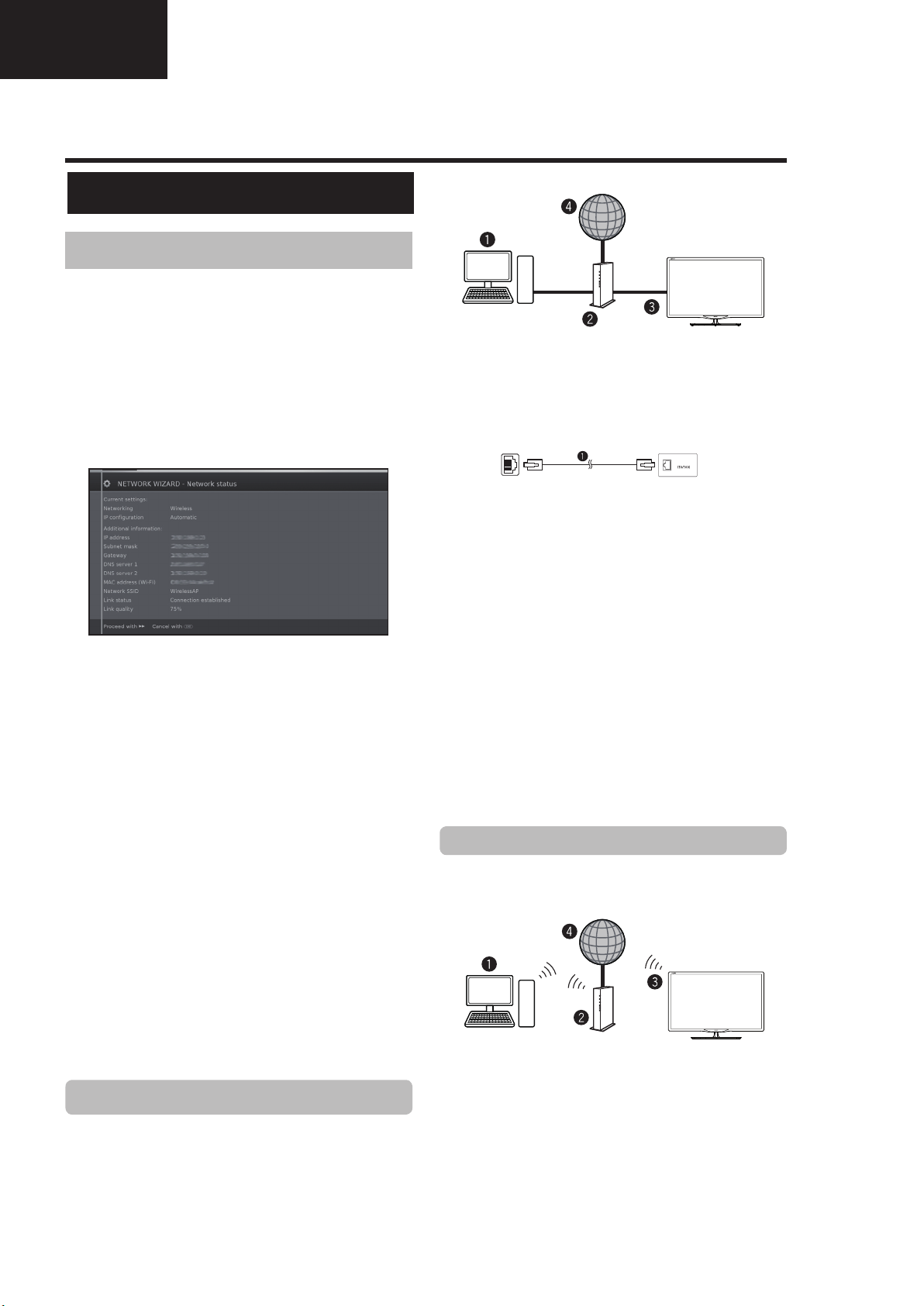
Network Setup
Connecting to the network
To enjoy internet services, you need to connect the TV
to a router with a high speed connection to the internet.
You can also connect the TV to your Home network
server through a router or access point.
The TV connection to the router can either be wired or
wireless.
To access the TV internet confi guration go to
Setup→Multimedia/Network→Network settings→
Networking. The next screen is shown:
Press J to continue the installation.
Choose between Wired or Wireless connection.
NOTE
• If you choose a wired connection to the router, you need
an ETHERNET cable (not included, commercially available).
• If you do not have a broadband internet connection, consult
the store where you purchased your TV or ask your internet
service provider or telephone company.
• Wired and wireless connection cannot be used at the same
time. Use only one of the connection types.
• A wireless LAN connection and performance cannot be
guaranteed for all residential environments. In the following
cases, the wireless LAN signal may be poor or drop, or the
connection speed may become slower.
- When used in buildings made with concrete, reinforced
steel, or metal.
- When placed near objects that obstruct the signal.
- When used with other wireless devices that emit the same
frequency.
- When used in the vicinity of microwave ovens and other
devices that emit a magnetic fi eld, electrostatic charge, or
electromagnetic interference.
• A stable connection speed is required to play back streaming
content. Use a wired LAN connection if the wireless LAN
speed is unstable.
Wired installation
Use an ETHERNET cable to connect the LAN terminal
on the TV to your broadcast router as shown below.
This is recommended when enjoying services which
require stable connection speeds, such as streaming
media.
● Wired connection overview
PC (Home Media Server)
Router (commercially available)
ETHERNET cable (commercially available)
Network (Internet)
● How to connect
lanimret NALretuoR
LAN
LAN
ETHERNET cable
1 Switch on the router (commercially available). Refer to
the router’s operation manual for switching on.
2 Connect the LAN terminal on the TV to the router
(commercially available) with an ETHERNET cable
(commercially available).
3 Go to Setup→Multimedia/Network→Network
settings→Networking.
4 Press OK and ▲/▼ to select “wired”, and then
press OK.
5 Select type of IP configuration:
Automatic: Automatic configuration of the IP
address via DHCP server or via multiple protocols
according to UPnP specification.
Manual: Enter your fixed static IP addresses
manually. (Ask your internet service provider).
6 Press OK.
Wireless installation
Use the SHARP (AN-WUD630) USB adapter with the
TV.
● Wireless connection overview
PC (Home Media Server)
Wireless LAN router/access point
Wireless
Network (Internet)
NOTE
• When using the SHARP wireless LAN adapter, try to provide
as much free space around the device for best performance.
• Make sure the firewalls in your network allow access to the
TV wireless connection.
AN-WUD630
LAN USB adapter
(Sold separately)
12
Page 13
Operation Manual (Continued)
Multimedia/Network Setup
LC-39/50LE650
LC-39/50LE651
LC-39/50LE652
• Operations cannot be guaranteed when used with access
points that do not have Wi-Fi® certification.
• A wireless LAN access point is required to connect the TV to
the Internet using a wireless LAN. See the operation manual
of your access point for setup.
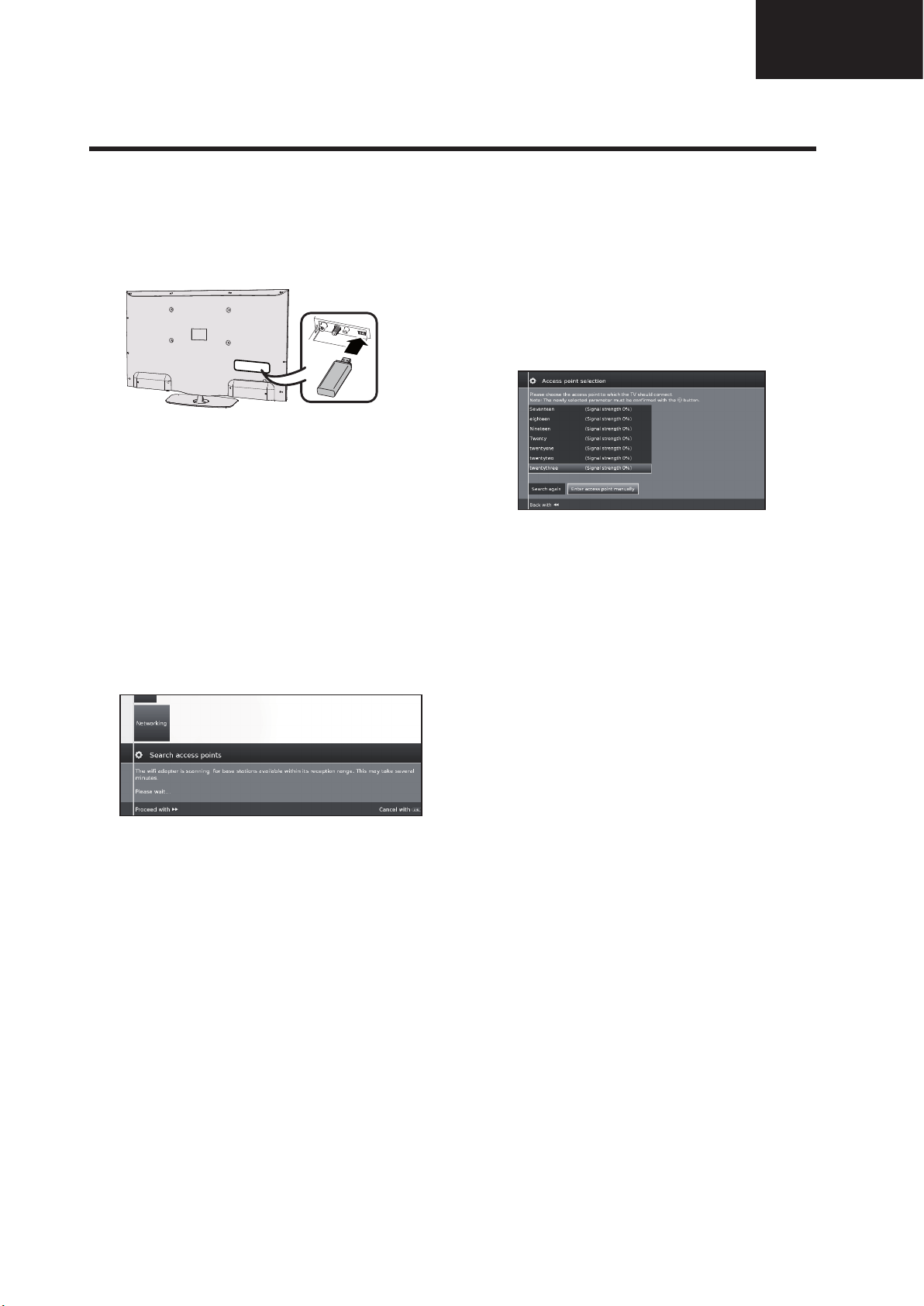
● How to connect
1 Switch on your router/access point before starting
the network installation.
2 Connect the
USB Wi-Fi port on the TV.
• Do not use a wireless LAN adapter other than the ANWUD630 Sharp wireless LAN adapter, as operations
cannot be guaranteed.
• If your wireless network is secured, have the
encryption key ready to enter on screen.
3 Go to Setup→Multimedia/Network→Network
settings→Networking.
4 Press OK and ▲/▼ to select “wireless”, and then
press OK.
The "Wireless" connection will be automatically selected
if the TV detects only the wireless USB adapter.
The TV starts to search for wireless routers/access points.
5 Select required router/access point and press OK.
As soon as ◄◄ is displayed , you can go back one
installation step by pressing this button.
6 If your network has an access code, it is necessary
to enter the code that allows access to the
network. A screen keyboard will appear to enter
the password.
Press OK.
7 Select IP address assignment method. You can
choose between: Automatic (DHCP) or Manual
(Input Static IP Address).
Automatic (DHCP): IP address is automatically
issued by a DHCP server on your home network.
• A DHCP server has to be set up on a device on
the network (WLAN router/access point).
Input Static IP Address: IP address is entered
manually. Use the RC alphanumeric buttons, to
input digits of IP address.
Press
J to continue.
Afterwards you will see a summary of the settings.
8 Press
J to confirm settings.
AN-WUD630
USB adapter to the
NOTES
• To connect your TV to the internet, you must have a
broadband internet connection.
• If you do not have a broadband internet connection, consult
the store where you purchased your TV or ask your internet
service provider or telephone company.
• There is no need to enter the security key for subsequent
connections to the wireless network.
If your access point is set to a stealth mode (Hidden
SSID, that prevents detection by other devices), you
need to use manual method to enter the SSID name for
desired access point.
1 Select Enter access point manually and press
OK. Introduce the SSID name using the on-screen
keyboard.
2 Select Adopt and press OK to fi x the name.
3 Select Encryption method and press OK.
Only if your access point is secured a WEP key or a
WAP password will be required.
4 Repeat the process from point 7 of previous
explanation.
To change wireless LAN connection settings, go to
Setup → Multimedia/Network → Network settings
→ Networking.
NOTES
• Any low bandwidth adapter (router, hub, wireless access
point,…) will show poor network connection and then, poor
streaming quality. It is recommended 56 Mbps or higher
bandwidth for full feature.
• Working in close proximity to other Wireless/Bluetooth
networks, may cause some trouble using a Wi-Fi adapter on
the internet connected TV. Because the wireless link cannot
be guaranteed, please try to change the Wi-Fi channel on
the Access Point (AP) to avoid interference. Please refer to
Access Point User Manual.
• Home Media (DLNA) requires external streaming media
software installed on a PC, inside the HOME Network, that
is not included with AQUOS NET+.
• Home Media (DLNA) server software as Windows Media
Player 11 (Windows Vista included) or Windows Media
Player 12 (Windows 7 included), TVersity (www.tversity.
com), Nero Media Home (www.nero.com), or Twonky Media
Manager (www.twonky.com) are preferred but others can
also be used. Visit the DLNA website (www.dlna.org) to see
the certifi ed media server list. Follow the server software’s
user manual for setup, share and stream media contents.
• Home Media (DLNA) (Video, Music and Photo) data is
organised in folders depending on the Server hierarchy;
options such as Artist, Genre, Composer, Ratings, Playlist
or Watch Folders may be present for sorting content, but
can be different depending on the selected Media Server.
• The “Play To” function of some PC Media Players may result
in very compressed video quality. For best video quality,
please use the USB Media Player function of the TV.
13
Page 14
LC-39/50LE650
LC-39/50LE651
LC-39/50LE652
Operation Manual (Continued)
TV menu options
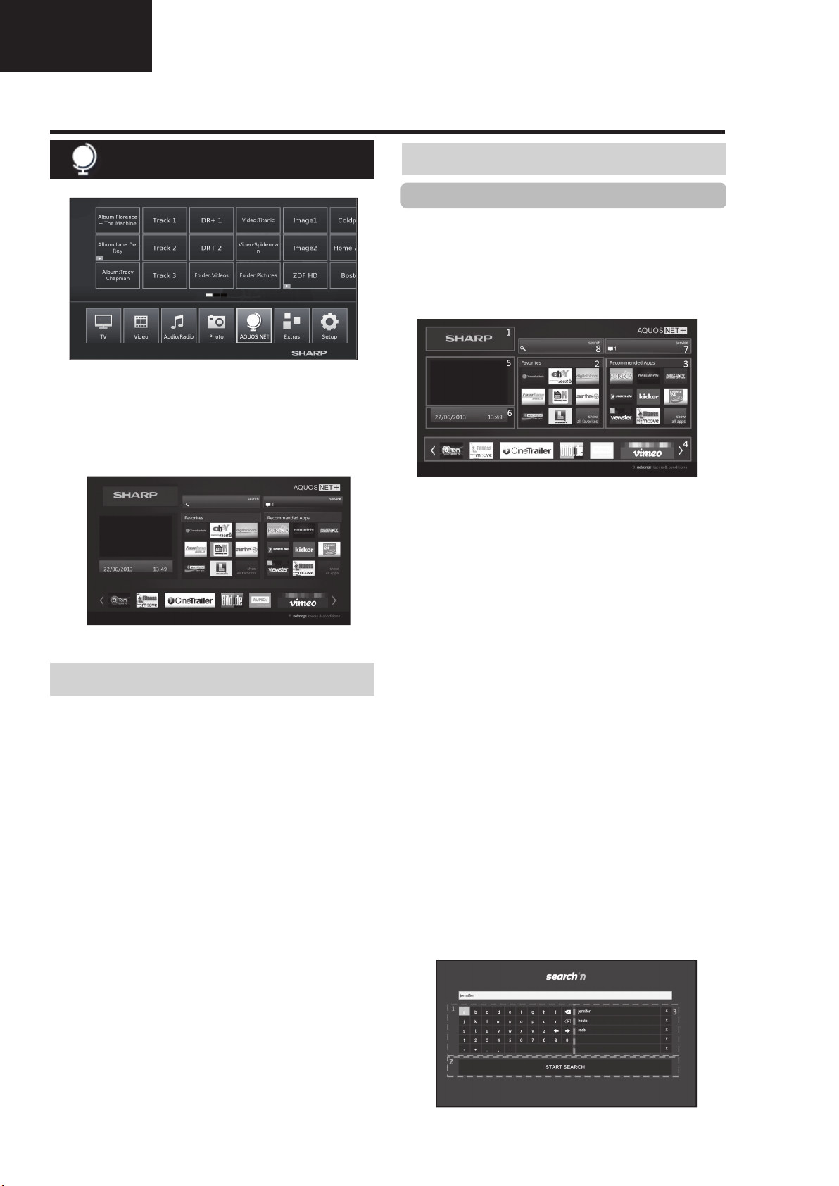
AQUOS NET+ function
AQUOS NET+ option allows you to access to AQUOS
NET+ feature and Internet browser.
For this option it is necessary that the TV set is
connected to Internet (See page 47).
1 Press @ button, select AQUOS NET+ and
press OK. The next screen appears:
2 Press > to exit.
What is AQUOS NET+?
Operations in AQUOS NET
+
Basic Operation
The illustrations on this page are for explanation
purposes. They are subject to change without notice.
E Display the AQUOS NET+ screen
Press NET on remote control or select AQUOS NET+
on main menu to open AQUOS NET+ home page.
AQUOS NET+ screen is organised into 8 areas:
AQUOS NET+ title banner
User-defined Favorites
Recommended Apps
Interactive windows for direct brand communications
or maintenance functions
Media window
Widget Area-real-time functions like date and time
or similar
Sharp Service Center
Interactive Search window
AQUOS NET+ is the feature that allows our Internet
connected TV sets to easily reproduce digital media
content coming from the Network. It provides access to
Internet services (Internet browser, YouTube, Facebook
and much more)
AQUOS NET+ provides a variety of services for each
country.
NOTES
• As AQUOS NET
over time to better serve its purpose.
• Some AQUOS NET
discontinued after some time.
+
is an online system, it can be modifi ed
+
services may be added, changed or
• Even in opern web-mode, users cannot download and save
fi les or install plugins.
DISCLAIMERS
• SHARP Corporation bears no responsibility regarding
the content and quality of the content provided by the
content service provider.
E Select a service
On AQUOS NET+ screen use▲/▼/◄/► to select the
desired service, and then press OK to start it.
• Press 6 to return to the previous page.
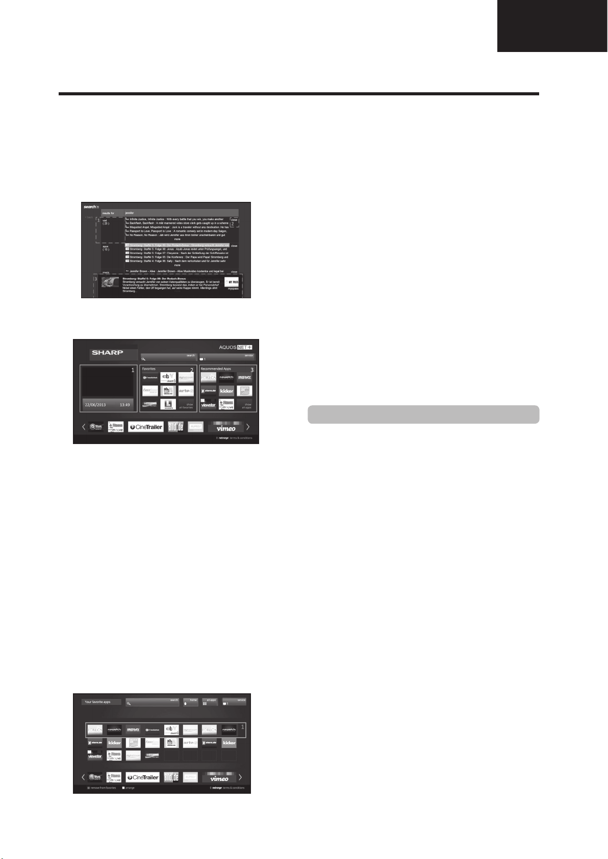
You can also use "Search" utility to fi nd specifi c services,
related to a search term.
•
Select "Search"
search page or start typing to directly search to
specific terms.
• T
o search for a specific keyword, the word is
entered using the virtual keyboard (1). The search
is executed by clicking Start Search (2). The history
of tthe last search terms can be found on the right
side (3).
and press OK to access the
14
Page 15
Operation Manual (Continued)
TV menu options
LC-39/50LE650
LC-39/50LE651
LC-39/50LE652
After searching for a specific term, the results are
categorized by their type (1), including the number
of search results. Categories can be hidden and
expanded on request by selecting the close button
(2) in the results overview.
Resting the cursor on a search result will bring up a
preview overlay (3) with information of the selected
content.
E User sections
The Home Screen is devided in 3 functional areas:
1 Interactive Media Area
This segment is used for the audio-visual
presentation of various types of content.
2 Favorite Apps Area
This area presents the top 8 apps of the userdefi ned favorite applications, including a link to
all user-defi ned favorite applications.
3 Recommended Apps Area
This area presents a selection of recommended
apps and also includes a link to the “all apps”
screen as described below.
In Area 2 and 3, please use ◄/►/▲/▼ to select a
service you want to access and press OK, direction
arrows appear around the service logo.
E Favorite Apps Screen
This screen gives an overview of all user-defi ned
favorites. Favorites can be selected in the all-apps
screen, as described below. The Top row of apps
is presented on the home-screen. The fi rst row
(1) is automatically presented in the favorite apps
section on the home screen.
Apps can be re-arranged by the user:
1
Move the cursor to the application that shall be moved.
2 Use Yellow color key to enter arrange-mode.
3 Move selected service to the desired position and
press the yellow color key again to confi rm the new
position.
To dismiss an application from the favorite Apps, place
the cursor on the respective app and press the RED
color-key on the remote control.
E Exit AQUOS NET+ screen
Press MENU button and select TV to return to tv mode.
You can also press AT V, DTV, SAT or RADIO button
to exit.
NOTES
• When connecting the TV to the Internet, a message which
requests a software update may be displayed in some
cases.
• Some services can request to the user to Login or create a
personal account. In this case, please follow the indication
on the screen.
• PREMIUM Video-on-Demand (VOD) services are available
in some countries.
• The illustrations on this page are for explanation purposes.
They are subject to change without notice.
• AQUOS NET+ screen language is adapted to the TV set
language previously selected.
• While AQUOS NET+ is active some TV menus or options
could be disabled.
Advance Operation
AQUOS NET+ uses alphanumerical characters within
some services, which can be introduced using the
remote numerical keys, in a similar way that people
use a mobile phone keypad. In order to make this
task easier, the LE650 is ready to use an external USB
keyboard (USB wired, USB-to-Wireless or USB-toBluetooth ready) to work only inside AQUOS NET+.
When an external keyboard is installed on TV set and
the user select AQUOS NET+, then the keyboard
mapping is:
(ENTER)/INTRO = OK (R/C). Used to enter inside
1
any service or to fix data once inside.
2 ◄/►/▲/▼ (U/O/I/K, or u/o/i/k for not extended
keyboard). Used to move between services or scroll
pages on Left/Right direction.
3 ESCape =6 (Return R/C). Return to previous page
on services.
4 (Backspace). Erase last character entered.
5 A..Z,a..z,0..9, and some US symbols (period or dot,
commercial at @, underscore, hyphen, exclamation,
question, colon, opening parenthesis, closing
parenthesis, number, slash, backslash, space).
Used for Login, Passwords, Date, and so.
NOTES
• The TV does not support hot plug connection of USB
devices like a keyboard. If you wish to connect any other
device, please do it when the TV is Power Off or in Standby.
• Inside AQUOS NET+ services, please use standard US
characters only (Not extended characters or Special
Country Language dependent), in order to avoid problems
with the applications.
• Using external USB keyboard is not possible to exit from
AQUOS NET+. If necessary, use the END remote key.
• Some types of keyboard could show incompatibilities or
try to use functions not supported by the TV.
15
Page 16
LC-39/50LE650
LC-39/50LE651
LC-39/50LE652
Operation Manual (Continued)
Quick guide
Initial auto installation
When the TV is powered on for the first time after
purchase, the initial auto installation wizard appears.
Follow the menus and make the necessary settings one
after another.
Confirm the following before turning
on the power
E Is the antenna cable connected?
E Is the AC cord plugged in?
1 Press a on the TV.
• The initial auto installation wizard appears.
• The auto installation can also be called in the TV menu,
see Repeat initial installation on page 40.
• The routine of the first installation wizard depends on
the selected settings.
2 Setting the menu language.
Press
a/b/c/d to select the desired language.
5 Select broadcast settings.
Press ▲/▼ to move between different tune type.
Press OK to select the desired antenna.
Cable analogue: analogue broadcast via cable/
DVB-T: Digital broadcast.
DVB-C: Cable digital broadcast.
DVB-S: Satellite broadcast.
antenna.
(Only 652/654 series
(Only 752/754 series)
Proceed with J button.
6 Select subtitles and audio languages.
Press
a/b/c/d and OK to select the desired
languages and alternative languages for subtitles
and audio for DVB programmes.
)
Proceed with
J button.
3 Setting Energy Efficiency.
Decide how efficiently you want to operate your TV
set.
•Home Mode:
The emphasis for home use is on low energy
consumption.
•Shop Mode:
The picture settings are aligned to operate in the
presentation room. If the ambient brightness diminishes,
the energy consumption is not reduced.
This setting can be changed later in the MENU
Extras→Energy Efficiency.
Proceed with J button.
4 Selecting the TV location.
Press ▲/▼/◄/► to select your country or area.
• This setting screen only appears during the initial auto
installation.
Proceed with J button.
Proceed with
•
To set up audio commentary for the visually impaired, please
see Audio commentary on page 25.
J button.
Setting options for DVB-T reception
If you have not selected DVB-T antenna in the antenna
selection, continue with Setting options for DVB-C
reception on page 10.
7 Selecting tuner settings.
● Scrambled stations
You can specify if coded stations are to be searched
for in the search/update.
Select yes to save all scrambled stations.
•
These stations can only be received in connection with a CI
module and the appropriate CA Card.
•
If a CI module with a CA Card is already inserted for the station
search, all the stations which this module can descramble are
also saved when no is selected.
● Search method
Select Frequency search if you want to run the
station search independently of the channel grid.
●
Accept logical channel number
In various countries, digital stations are transmitted
with a preset channel number per station, known as
"Logical Channel Numbers" (LCN).
If you select yes, these default channel numbers will
be used and the channels will be sorted as per LCN.
16
Page 17
Operation Manual (Continued)
Quick guide
LC-39/50LE650
LC-39/50LE651
LC-39/50LE652
8 Supplying power to the antenna.
If you use a DVB-T antenna that requires a supply voltage
and which is not supplied via a power adapter, then select
yes (5V) for the antenna's power supply.
Press J button.
How to align your DVB-T antenna is described on
page 14.
9 Continue with Settings for all types of reception
(See page 13).
Setting options for DVB-C reception
If you have not selected DVB-C antenna in the
antenna selection, continue with Setting options for
DVB-S reception below.
The normal DVB-C settings are derived from the
selection of the location and do not need to be changed.
Press ▲/▼/◄/► to change each item to the appropriate
settings:
● Network selection
If several networks are available via DVB-C, you
can decide which network you want to receive your
channels from.
● Scrambled stations
You can specify if coded stations are to be searched
for in the search/update.
Select yes to save all scrambled stations.
•
These stations can only be received in connection with a CI
module and the appropriate CA Card.
•
If a CI module with a CA Card is already inserted for the station
search, all the stations which this module can descramble are
also saved when no is selected.
● Search method
If you select Frequency Search, a search is
performed for all receivable stations. With Network
Search, only the stations which the networks
supply are searched, either for all receivable
networks or only for the particular network specified
under Network ID.
● Start Frequency
The DVB stations are only searched for in the
frequency range above the start frequency.
● Network ID
Change this setting to register only the specified
network ID.
● Accept logical channel number
In various countries, digital stations are transmitted
with a preset channel number per station, known as
"Logical Channel Numbers" (LCN).
If you select yes, these default channel numbers will
be used and the channels will be sorted as per LCN.
NOTE
• The value of Frequency and Network ID should
be set to the value specified by the cable provider.
Press
J to continue.
Setting options for DVB-S reception
If you have not selected a DVB-S antenna in the
antenna selection, continue with Settings for all types
of reception on page 13.
Select the satellite system.
Specify how you receive which satellite(s) (single
satellite or type of satellite system). Ask your dealer in
this regard.
The normal DVB-S settings are derived from the
selection of the location and do not need to be changed
in most cases.
●
Single satellite
Reception of a single satellite via a connected LNC
(LNB). See page 11 for settings.
●
2 satellites on 22kHz switchbox
Reception of two different satellites with two LNCs
(LNBs) which are connected to the TV set by a 22
kHz switchbox. See page 11 for settings.
●
2 satellites on Toneburst switch
Reception of two different satellites with two LNCs
(LNBs) which are connected to the TV set by a
toneburst switch. See page 11 for settings.
●
Max. 4 satellites on DiSEqC multiswitch
The TV set controls a DiSEqC multiswitch to which
up to four LNCs (LNBs) for different satellites are
connected. See page 11 for settings.
●
DiSEqC one cable communal system
Select setting if the TV set is connected to a DiSEqC
single cable system (according to EN50494). Several
satellite receivers can be connected to one satellite
cable. See page 12 for settings.
●
Other communal installation
Select this setting if the TV set is connected to a
single-cable system (without DiSEqC). Several
satellite receivers can be connected to one satellite
cable. As opposed to a DiSEqC one cable system
there are restrictions in the range of certain reception
frequencies in common single-cable community
systems. See page 13 for settings.
Press
J to continue
17
Page 18
LC-39/50LE650
LC-39/50LE651
LC-39/50LE652
Operation Manual (Continued)
Quick guide
Setting options for Single satellite
Reception of a single satellite via a connected LNC
(LNB).
1 Select satellite.
Press
J to continue.
2 Select Dual Band (low/high) or Single Band.
Here you specify if you use a Dual Band (Universal)
LBN or Single LBN.
Setting options for 2 satellites on 22kHz
switchbox / 2 satellites on Toneburst switch
1 Select Satellite1/Satellite2
2 Select satellite name from list and press OK.
Press
3 Specify here the oscillator frequency for your LNB.
J to continue.
Press
J to continue.
3 Specify here the oscillator frequency for your LNB.
Normally you do not need to change the values
for high and low band, unless the LNB of your
satellite system uses a different oscillator frequency
(important for the frequency display).
If you use the setting Single Band in step Dual/
Single Band, you only have to define the LNB
frequency for the Low Band.
4 Press
See Setting options for all DVB-S reception on
page 13 to continue.
J to continue.
Normally you do not need to change the values
for high and low band, unless the LNB of your
satellite system uses a different oscillator frequency
(important for the frequency display).
4 Press OK to select frequency and press
continue.
See Setting options for all DVB-S reception on
page 13 to continue.
J to
Setting options for Max. 4 satellites on DiSEqC
multiswitch
Select DiSEqC multiswitch and adpat settings for this
selection.
18
Page 19
Operation Manual (Continued)
Quick guide
LC-39/50LE650
LC-39/50LE651
LC-39/50LE652
● Repeat rate
The refresh rate determines how often a DiSEqC
command is output. A refresh is only necessary with
cascaded system.
● Control voltage
The control voltage controls the switch of the
polarisation level (horizontal/vertical) in non-DiSEqC
capable components (e.g., control of single LNBs
via DiSEqC multiswitch).
● 22kHz signal
The 22kHz signal controls the switching between
high and low band in the Band setting. The Position
setting controls the selection of the satellites in nonDiSEqC capable components.
● Toneburst
The Toneburst controls the selection of the satellites
in non-DiSEqC but Toneburst capable components
with the Position and Option settings.
Press OK to adopt settings and press J to continue.
1 Select Satellite1 to Satellite4.
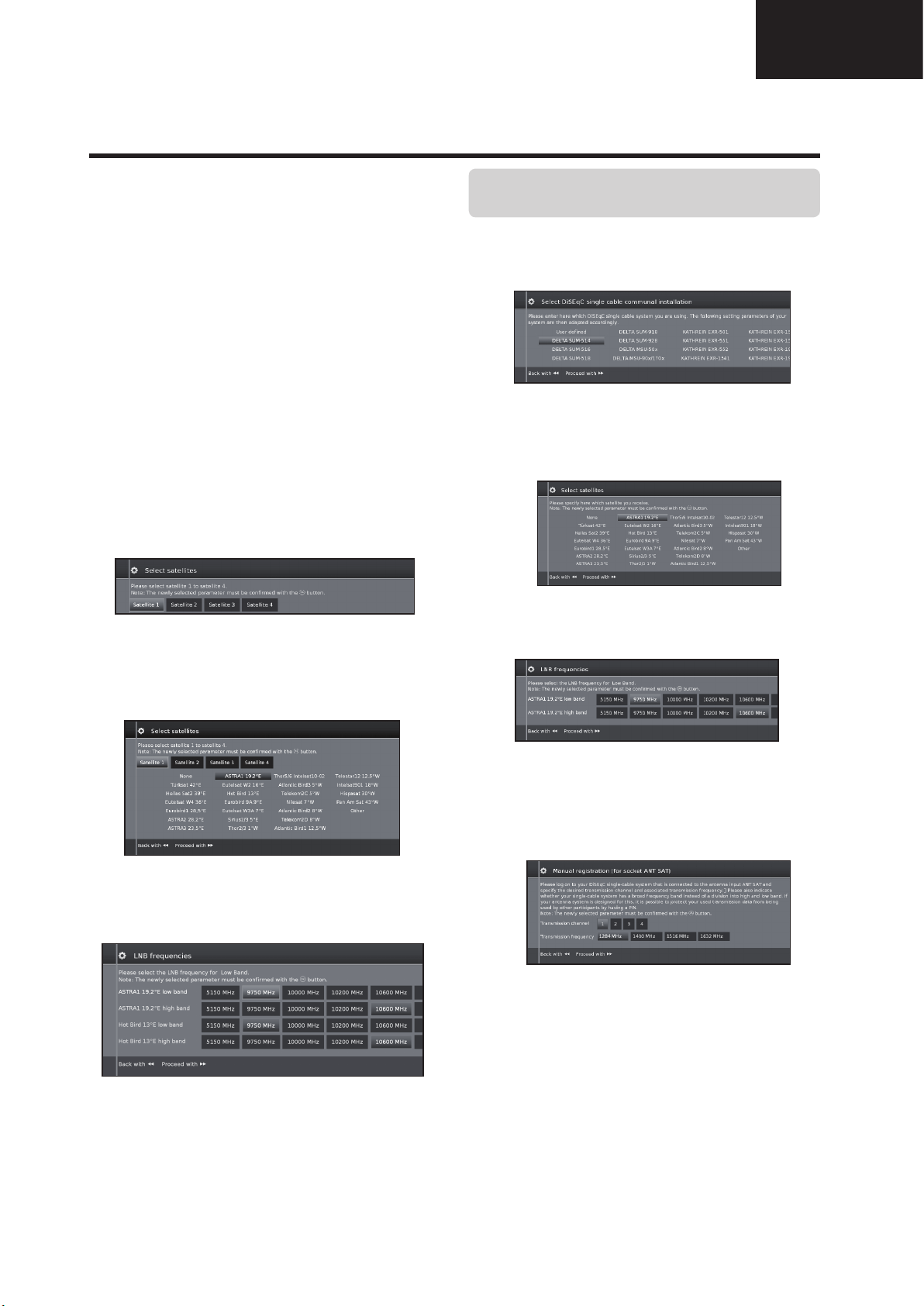
Setting options for
DiSEqC one cable
communal system
1 Select which DiSEqC single cable system you are
using and press OK.
2 Select satellite name from list and press OK. Press
J to continue.
3 Specify here the oscillator frequency for your LNB
and press OK. Press
J to continue.
2 Select satellite name from list and press OK. Press
J to continue.
3 Specify here the oscillator frequency for your LNB.
Normally you do not need to change the values
for high and low band, unless the LNB of your
satellite system uses a different oscillator frequency
(important for the frequency display).
See Setting options for all DVB-S reception on
page 13 to continue.
Normally you do not need to change the values
for high and low band, unless the LNB of your
satellite system uses a different oscillator frequency
(important for the frequency display).
4 Select and adjust settings for DiSEqC single cable
communal installation.
Select the desired transmission channel and the
corresponding transmission frequency.
PIN protection
If your system is designed for it, it is possible to
protect your used transmission data from use by
other subscribers with a PIN.
Define/change PIN
Here you can determine and change the PIN for
PIN protection. Only possible when yes has been
selected for PIN protection.
Continue with Setting options for all types of
reception on page 13.
19
Page 20

LC-39/50LE650
LC-39/50LE651
LC-39/50LE652
Operation Manual (Continued)
Quick guide
Setting options for Other communal installation
1 Select satellite.
Press
J to continue.
2 Specify here the oscillator frequency for your LNB.
If your set is connected to a single-cable system
without external voltage supply, you can connect
the antenna supply (13V or 18V / max. 450mA)
with 13V or 18V.
● Scrambled stations
Select yes to save all scrambled stations.
• These stations can only be received in connection
with a CI module and the appropriate CA Card.
• If a CI module with a CA Card is already inserted
for the station search, all the stations which this
module can descramble are also saved when no
is selected.
●
Search method
If you select Frequency Search here, a search is
performed for all receivable stations. With Network
Search, from all receivable networks all the stations are
searched which are supplied by these networks.
●
Symbol rate
The symbol rate is specified by the satellite provider and
normally does not need to be changed.
●
Accept Logical Channel Number
This setting allows you to decide whether you want to
accept the Logical Channel Number (LCN).
Press
J to continue.
Continue with Setting options for all types of
reception below.
Setting options for all types of reception
Continue with Setting options for DVB-S reception
below.
Setting options for DVB-S reception
●
Network selection
If several networks are available via DVB-S, you
can decide which network you want to receive your
channels from.
●
Settings
If several satellites are received, the following settings
must be made for every satellite. The type of settings
available may differ depending on the selected satellite
or network.
●
Age related lock
Allows you to restrict programmes depending on the age
classification.
The information about age classification is provided by
the broadcasting station.
The stations locked can only be watched after entering
the access code (see page 24).
●
Time and date
Enter the correct values with the numeric buttons here.
● Network configuration
Here you can now specify if you wish to configure a
network "Configure now" (see page 47) or you wish
to configure it later "Do not configure or configure
later".
20
Page 21
Operation Manual (Continued)
Quick guide
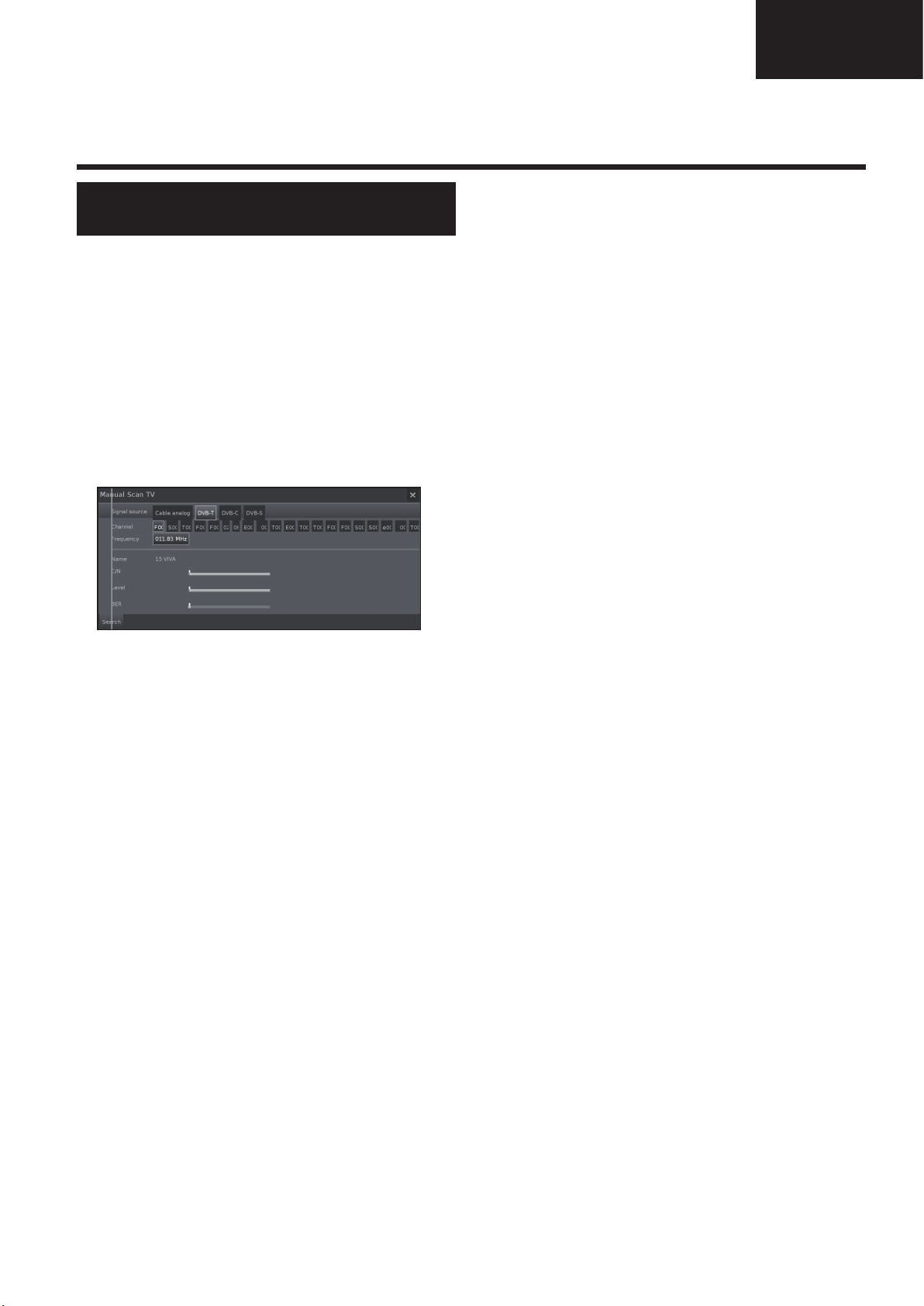
Positioning / aligning DVB-T
antenna
If you install a DVB-T/T2/S/S2 antenna for the first time
or relocate it, you should adjust the alignment of the
antenna to receive a good reception while checking the
antenna setup screen.
In normal TV mode, without other displays, a DVB-T
station is received and selected.
1 Select Setup.
2 Select Stations.
3 Select Manual Scan TV.
LC-39/50LE650
LC-39/50LE651
LC-39/50LE652
Position and align the antenna in such a manner that
maximum values for C/N and Level are obtained.
The value for BER should be as low as possible.
4 Select Search and press OK to start search.
21
Page 22
LC-39/50LE650
LC-39LE650E/V LC-50LE650E/V
LC-39LE651E/K/V LC-50LE651E/K/V LC-60LE651E/K
LC-39LU651E LC-50LU651E LC-60LU651E
LC-39LE652E/V LC-50LE652E/V LC-60LE652E
LC-39LM652E/V LC-50LM652E LC-60LM652E
LC-39LK652E LC-50LK652E LC-60LK652E
LC-39LX652E LC-50LX652E LC-60LX652E
LC-39LE654E/V LC-50LE654E/V LC-60LE654E
LC-39/50LE651
LC-39/50LE652
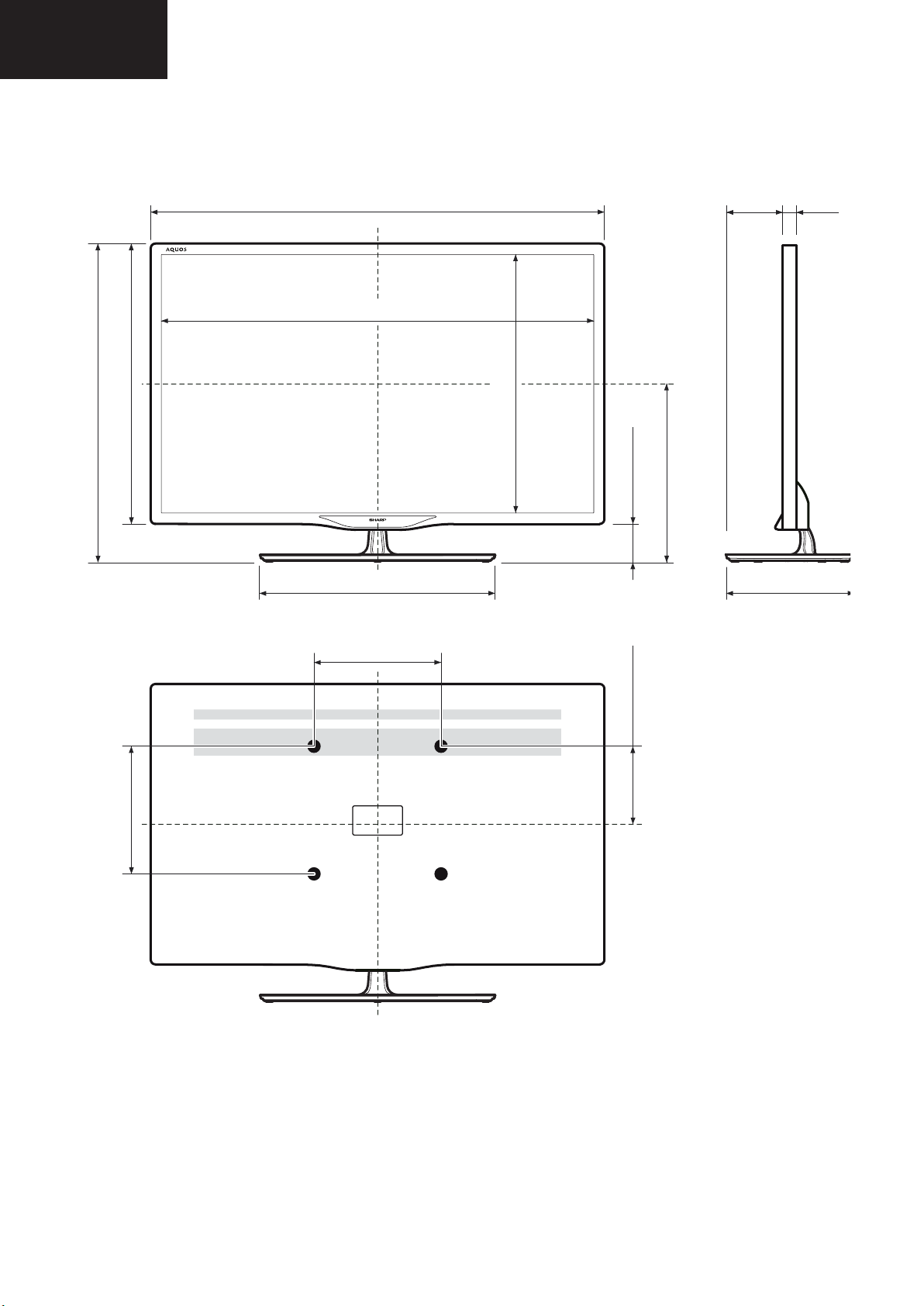
DIMENSIONS
(881) / [1123] / [(1368)]
(859) / [1100] / [(1335)]
(517) / [654] / [(798)]
(590) / [727] / [(871)]
(457) / [485] / [(585)]
(483) / [620] / [(754)]
(73) / [74] / [(73)]
(337) / [406] / [(478)]
(83)
[88]
[(125)]
(242) / [265] / [(308)]
(41)
[41]
[(41)]
(200) / [200] / [(400)]
(200) / [400] / [(400)]
(183) / [206] / [(230)]
39”: ( )
50”: [ ]
60”: [( )]
22
Page 23
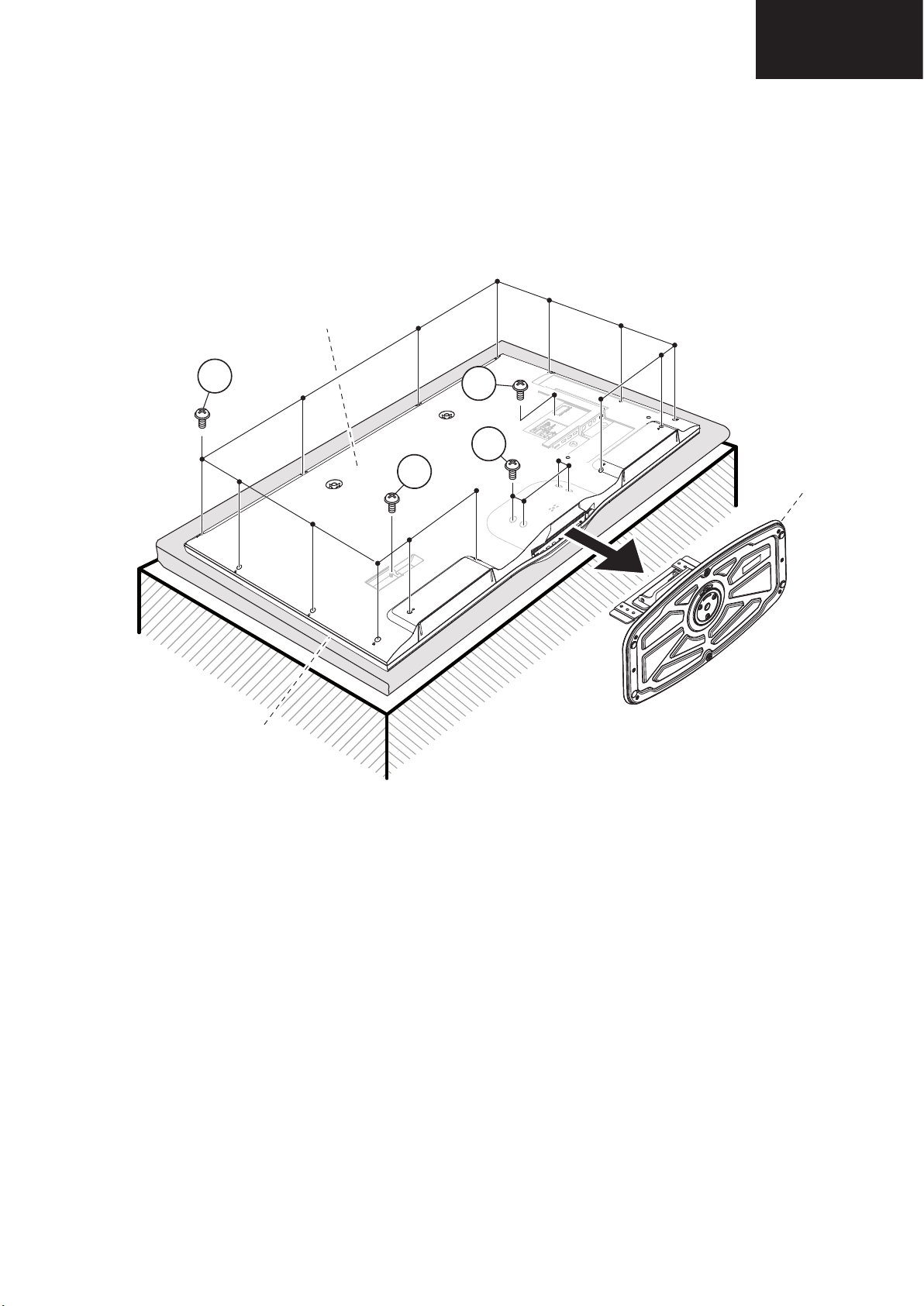
1. Removing of major Parts 39”
LC-39LE650
1 / 5
LC32D44E-BK
Service Manual
CHAPTER 2.
REMOVING OF MAJOR PARTS
[1] REMOVING OF MAJOR PARTS
1. Remove the 4 lock screws and detach the Stand.
2. Remove the 14 lock screws , 1 lock screw , 1 lock screw and detach the AC cord cover and the Rear Cabinet.
2
1
3
4
2
front
CABINET
rear
CABINET
1
3
4
STAND
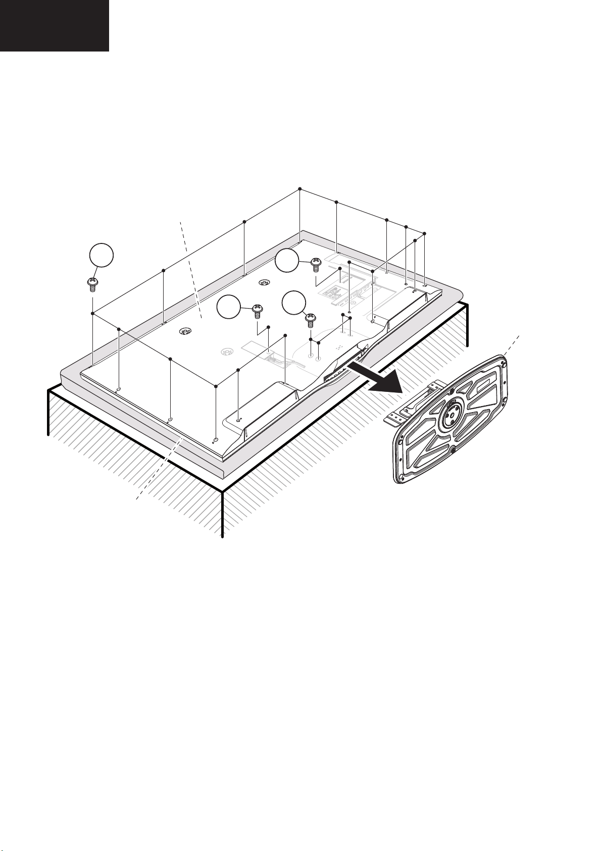
1.1. Remove the 4 lock screws and detach the Stand.
1.2. Remove the 14 lock screws , 1 lock screw , 1 lock screw and detach the AC cord cover and Rear Cabinet
REMOVING OF MAJOR PARTS
LC-39/50LE650
LC-39/50LE651
LC-39/50LE652
23
Page 24
LC-39/50LE650
AC CORD
Power unit
P802
P801
[EL]
SC101
[LA]
[PD]
Main unit
[LV]
[PD]
[SP]
[LW]
[LA]
[RA]
[LW]
[LV]
SPEAKER -R
SPEAKER -L
LC-39/50LE651
LC-39/50LE652
1. Removing of major Parts 39” (Continued)
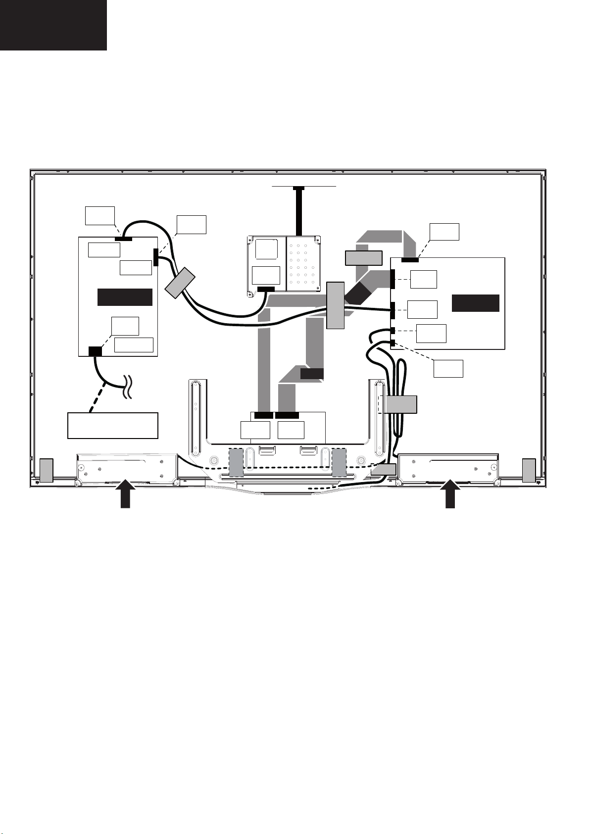
1.3. Disconnect all the connectors from all the PWBs.
24
Page 25
1. Removing of major Parts 39” (Continued)
LC-39LE750
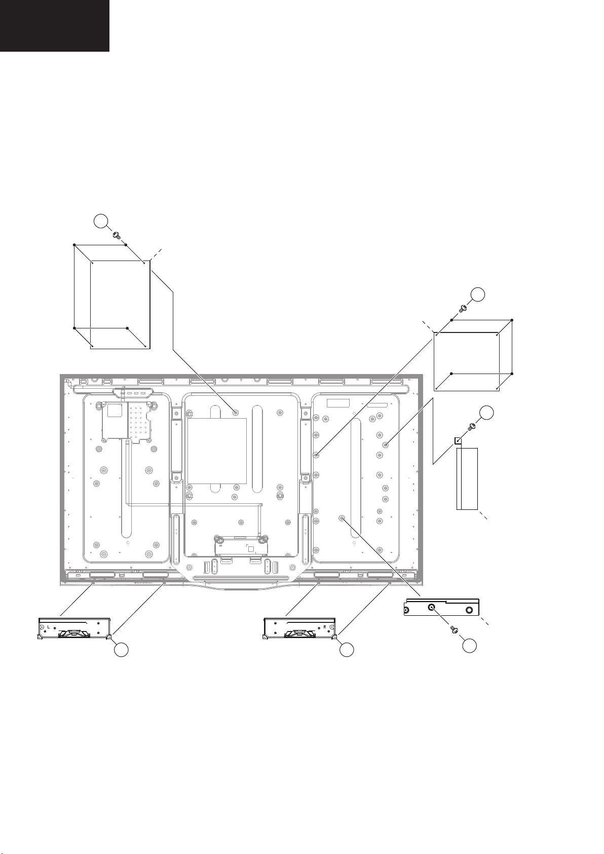
4. Remove the 4 lock screws and detach the POWER unit.
5. Remove the 4 lock screws and detach the MAIN unit.
6. Remove the 1 lock screws and detach the terminal BRACKET.
7. Remove the SPEAKER-L and SPEAKER -R .
7
8
6
5
9
1.4. Remove the 4 lock screws and detach the POWER unit.
1.5. Remove the 4 lock screws and detach the MAIN unit.
1.6. Remove the 1 lock screw and detach the terminal BRACKET.
1.7. Remove the SPEAKER-L and SPEAKER-R .
5
LC-39/50LE650
LC-39/50LE651
LC-39/50LE652
6
terminal
9
8
7
BRACKET
25
Page 26
LC-39/50LE650
Service Manual
8. Remove the 4 lock screws and detach the stand BRACKET.
9. Remove the 2 lock screws and detach the control button HOLDER.
10. Detach the KEY unit and the piramid lighting DIFFUSER .
11
13
12
10
LC-39/50LE651
LC-39/50LE652
1. Removing of major Parts 39” (Continued)
1.8. Remove the 4 lock screws ⑩ and detach the stand BRACKET.
1.9. Remove the 2 lock screws ⑪ and detach the control button HOLDER.
1.10. Detach the KEY unit ⑫ and the pyramid lighting DIFFUSER ⑬.
11
control
button
HOLDER
KEY
unit
stand
BRACKET
13
12
piramid
lighting
DIFFUSER
10
26
Page 27
1. Removing of major Parts 39” (Continued)
LC-39LE650
14
1.11. Detach the LCD module ⑭ from the front CABINET.
LC-39/50LE650
LC-39/50LE651
LC-39/50LE652
14
27
Page 28
LC-39/50LE650
LC-50LE650
LC32D44E-BK
Service Manual
CHAPTER 2. REMOVING OF MAJOR PARTS
[1] REMOVING OF MAJOR PARTS
1. Remove the 4 lock screws and detach the Stand.
2. Remove the 14 lock screws , 1 lock screw , 1 lock screw and detach the AC cord cover and the Rear Cabinet.
2
1
3
4
STAND
LC-39/50LE651
LC-39/50LE652
2. Removing of major Parts 50”
2.1. Remove the 4 lock screws and detach the Stand.
2.2. Remove the 14 lock screws , 1 lock screw , 1 lock screw and detach the AC cord cover and Rear Cabinet
rear
CABINET
2
4
3
1
STAND
1 / 5
front
CABINET
28
Page 29
2. Removing of major Parts 50” (Continued)
Service Manual
2.3. Disconnect all the connectors from all the PWBs.
LC-39/50LE650
LC-39/50LE651
LC-39/50LE652
AC CORD
P802
P801
Power unit
[EL]
SC101
[LW]
[LA]
[PD]
[LV]
[LW]
[LV]
Main unit
[PD]
[SP]
[RA]
SPEAKER -R
SPEAKER -L
29
Page 30
LC-39/50LE650
LC-50LE650
7
8
6
5
10
9
LC-39/50LE651
LC-39/50LE652
2. Removing of major Parts 50” (Continued)
2.4. Remove the 4 lock screws and detach the POWER unit.
2.5. Remove the 4 lock screws and detach the MAIN unit.
2.6. Remove the 1 lock screw and detach the side BRACKET.
2.7. Remove the 1 lock screw and detach the bottom BRACKET.
2.8. Remove the SPEAKER-L and SPEAKER-R .
5
POWER
unit
6
MAIN
unit
7
side
BRACKET
SPEAKER -R
bottom
BRACKET
10
SPEAKER -L
9
8
30
Page 31

2. Removing of major Parts 50” (Continued)
LC-50LE650
Service Manual
9. Remove the 10 lock screws and detach the stand BRACKET.
10. Remove the 2 lock screws and detach the control button HOLDER.
11. Detach the KEY unit and the piramid lighting DIFFUSER .
12
14
13
11
2.9. Remove the 6 lock screws ⑪ and detach the stand BRACKET.
2.10. Remove the 2 lock screws ⑫ and detach the control button HOLDER.
2.11. Detach the KEY unit ⑬ and the pyramid lighting DIFFUSER ⑭.
LC-39/50LE650
LC-39/50LE651
LC-39/50LE652
14
13
piramid
lighting
12
KEY
control
button
HOLDER
DIFFUSER
unit
stand
BRACKET
11
31
Page 32

LC-39/50LE650
LC-50LE650
15
LC-39/50LE651
LC-39/50LE652
2. Removing of major Parts 50” (Continued)
2.12. Detach the LCD module ⑮ from the front CABINET.
front
CABINET
15
LCD
module
32
Page 33

LC-39/50LE650
LC-39/50LE651
LC-39/50LE652
SERVICE ADJUSTMENTS
1. Adjustment method after PWB and/or IC replacement due to repair
The unit is set to the optimum performance at the time of shipment from the factory.
If any value should become improper or any adjustment is necessary due to the part replacement, make an adjust-
ment according to the following procedure.
1.1. Procure the following units in order to replace the main unit:
MAIN UNIT DUNTKG135FNxx
NOTE: [Caution when replacing ICs in the main unit (IC0503, IC1507, IC1508, IC1509, IC1510)]
Before replacing the relevant part, procure the following parts in which the data have been rewritten.
Ref. Description Parts code IC + data Description new IC code for service
IC0503 PC EDID LE65x/75x RH-IXD660WJZZY VHIBR24T02J-1Y File: LE65x_VGA_v1.bin
IC1507 HDMI1 EDID LE65x/75x RH-IXD661WJZZY VHIBR24T02J-1Y File: LE65x_HDMI1_v1.bin
IC1508 HDMI3 EDID LE65x/75x RH-IXD663WJZZY VHIBR24T02J-1Y File: LE65x_HDMI3_v1.bin
IC1509 HDMI4 EDID LE65x/75x RH-IXD664WJZZY VHIBR24T02J-1Y File: LE65x_HDMI4_v1.bin
IC1510 HDMI2 EDID LE65x/75x RH-IXD662WJZZY VHIBR24T02J-1Y File: LE65x_HDMI2_v1.bin
2. Entering and exiting the adjustment process mode. Standard method.
1. By key-unit.
1. Unplug the AC power cord, plug the AC power cord and wait until pyramid led blue is iluminated and then:
2. Press and hold “V-” and “CH-” keys, simultaneously.
3. “SHARP FACTORY MENU” appears (see Figure 1).
4. Unplug the AC power cord to exit of adjustments process.
2. By own R/C
1. Turn on the TV set.
2. Press “MENU”.
3. Press “9”, ”9”, ”9”, “2”, “2”, “2” (to enter this code the time is limited to 5 sec. approx.)
4. “SERVICE MENU” appears (see Figure 1).
5. Press ◄/► cursor to select the desired function.
6. Press “OK on boxes to go to submenu.
7. Press “6” to return to “SHARP FACTORY” Main Menu.
8. Press”END” or “MENU” to exit of adjustments mode.
33
Page 34

LC-39/50LE650
LC-39/50LE651
LC-39/50LE652
3. Remote control key operation in Service Mode (Adjustment process mode).
Remote Control key Keyboard unit Function
Cursor (◄/►) Moving an item by one (LEFT/RIGHT) on “Service Menu”.
Moving an item by one (LEFT/RIGHT) on SubMenus.
Moving a Slider Horizontal Bar to select a value on SubMenu Function.
Cursor (▼/▲ ) Enter on a SubMenu (▼).
Exit from a SubMenu (▲).
Exit of Service Mode (Adjustment mode).
OK Selecting a MENU on “Service Menu”
Selecting a SubMenu.
Executing a function on a SubMenu.
MENU MENU Exit of Service Mode (Adjustment mode).
Return to “Service Menu” from a SubMenu.
0..9
i ( k / l) VOL
P (r / s)
b
CH
INPUT
( k / l)
(r / s)
Enter numeric data on SubMenu Function.
Volume UP or DOWN.
Channel UP or DOWN (Only in ATV/DTV mode), otherwise no action.
No action
The required input mode should be switched previously to enter the Service Mode.
CAUTION: Use due care in handling the information described here lest the users should know how to enter the
adjustment process mode. If the settings are tampered with in this mode, unrecoverable system
damage may result.
4. Description of display
Figure 1: Main Service Adjustment Menu
Service
System
Data
In gure 1 the selected Menu is remarked by CYAN color, but same criteria is valid on internal SubMenus.
Please use the remote keys as is explained in “3. Remote control key operation in Service Mode” to access to all the options
described below.
GUI
Exception
Chassis
Options
Station
list
DVB
EPG
34
Page 35

4. Description of display (continued)
ServiceMenu SubMenu Options1 Options2 Comments
LC-39/50LE650
LC-39/50LE651
LC-39/50LE652
SystemData Package
MainSystem
Rfs
Opt
MainBootloader
Standby
Controller
WiFiModule
GUI Don’tuse
Exception WritetoUSB
Chassis
Options
ChassisDummy 0 Don’tuse
CiOptions 0
FactoryMode 0
InitialInst 0
MpegDeblocking 0
MpegDeringing 0
NoAudioDelay 0
0.1.18.1
1.18.0.0
1.18.0.0
1.18.0.0
0.93.2.0
0.0.23.2
0.0.0.0
MAINVERSION
SoC
STM8VERSION
InsertaUSBFlash
memoryto
capturethe
exceptionfiles
0:normal
operation
1:disableCiPlus
0:normal
operation
1:factorymode(
KModeon)
0:TVsetstarts
normally
1:TVsetstarts
withinitial
installationmenu
Enable/Disable
mpegdeblocking
settingsforSD
services.
0:none
1:low
2:medium
3:high
Enable/Disable
mpegderinging
settingsforSD
services.
0:none
1:low
2:medium
3:high
Disableallaudio
delay
0:audiodelay
enabled
1:audiodelay
disabled
35
Page 36

LC-39/50LE650
LC-39/50LE651
LC-39/50LE652
4. Description of display (continued)
ServiceMenu SubMenu Options1 Options2 Comm e n t s
NoAutoPowerOff 0
NoWSS 0
OldSwVersions 0
Panel200Hz 0 Don’tuse
0:autopoweroff
enabled(4h,
withoutsync)
1:allautopower
offfunctions
disabled
Disablewide
screensignaling
(WSS)evaluation
(Scartand
analoguetuner)
0:WSSevaluation
enabled
1:WSSinfois
ignoredforvideo
scaling.Insteadof
WSSinfouser
settingbecomes
active
Installingold
softwareversions
allowed
0:normal
operation‐only
newersoftwareis
accepted
1:oldersoftwareis
accepted,too
Panel3D 1Don’tuse
PanelHFlip 0 Don’tuse
PanelVFlip 0Don’tuse
RC5‐Mapping 0 Don’tuse
RC5‐Subsystem 0Don’tuse
Service1 0 Don’tuse
SysTimeSource 0
Selectthesource
ofthesystemtime
information
0:timesource
automatic
1:usetheinternal
realtimeclock
2:useNTP
(networktime
protocol)
3:usethetime
formDVB
transportstream
36
Page 37

4. Description of display (continued)
ServiceMenu SubMenu Options1 Options2 Comm e n t s
LC-39/50LE650
LC-39/50LE651
LC-39/50LE652
WarmupMode
1
StationList StationImport
StationExport
DeleteStation
List
Chassis Don’tuse
DVB DVBInfo
Tuner1Info
Tuner2InfoDon’tuse
ATV/DVBTuner
ServiceInfoBox
0:normal
operation
1:automatically
switchonafter
poweron
InsertUSBFlash
memorytoimport
astationmapfrom
externalfile.
InsertUSBFlash
memorytosave
thecurrentTV
stationmapona
externalfile.
Deletethecurrent
TVstationmap.
VideoInfo VideoInfoBox
AudioInfo AudioInfoBox
PCRInfoDon’tuse
Common
Interface
EPG DVB Don’tuse
DeleteCI+
authentication
contexts
ShowCI+
information
CI+information
DeviceID
Validfrom
Validto
Don’tuse
(Engineering
Purpose)
Don’tuse
(Engineering
Purpose)
Don’tuse
(Engineering
Purpose)
Don’tuse
(Engineering
Purpose)
Don’tuse
(Engineering
Purpose)
ResetUpdate
Date
ClearEPG
database
ResetUpdateEPG
timer
ClearinternalEPG
database
37
Page 38

LC-39/50LE650
LC-39/50LE651
LC-39/50LE652
4. Description of display (continued)
ServiceMenu SubMenu Options1 Options2 Comments
PQSettings
PublicMode
ImportEPG
database
ExportEPG
database
PUBLICMODE
PowerOnfixed Variable
Maximum
volume 100 0…100
Volumefixed Variable
Volumefixed
level 33 0…100
RCbutton Respond
Panelbutton Respond
MenuButton Respond
Variable
Fixed
Variable
Fixed
Respond
Norespond
Respond
Norespond
Respond
Norespond
Importexternal
EPGdatabasefrom
USBfile.
ExportEPG
internaldatabase
toaUSBfile.
Don’tuse
(Engineering
Purpose)
SeePublicMode
Description
Use◄/► toadjust
and“OK”tofix
value
Enternumberof
maximumvolume
Use◄/►toadjust
and“OK”tofix
value
Enternumberof
maximumvolume
Use◄/►toadjust
and“OK”tofix
value
◄/►toadjust
Use
and“OK”tofix
value
Use◄/►toadjust
and“OK”tofix
value
OnScreen
Display Yes
Inputmodestart Normal
InputTVmode
programnumber
0
Yes
No
Normal
ATV
DTV
HDMI1
HDMI2
HDMI3
HDMI4
SCART‐AV
VIDEO
PCIN
COMPONENTS
0…9999
38
Use◄/►toadjust
and“OK”tofix
value
◄/►toadjust
Use
and“OK”tofix
value
Enternumberof
program
Page 39

4. Description of display (continued)
ServiceMenu SubMenu Options1 Options2 Comments
Inputmodefixed Variable
RCpaththrough Off
Hotelmode Off
RS232CPower
On
HDMILevel
PowerOn
Commit
Reset
Cancel
WhiteBalance MGAMMAReset
MGAMMA
Pattern
MGAMMAIN1
MGAMMAIN2
MGAMMAIN3
MGAMMAIN4
MGAMMAIN5
MGAMMAIN6
MGAMMAINR1
MGAMMAING1
Variable
Fixed
On
Off
On
Off
Disable
Disable
Pattern1
Pattern2
Pattern3
Pattern4
Pattern5
Pattern6
160 0...1023
320
480
640
800
960
571 0...4096
614
Enable
Disable
Enable
Disable
0...1023 Pattern2
0...1023 Pattern3
0...1023 Pattern4
0...1023 Pattern5
0...1023 Pattern6
0...4096
Use
and“OK”tofix
value
Use◄/►toadjust
and“OK”tofix
value
(Needadditional
Hardware)
Use
and“OK”tofix
value
Use◄/►toadjust
and“OK”tofix
value
(Needadditional
Hardware)
Use
and“OK”tofix
value
(Needadditional
Hardware)
Press"OK"to
confirmchanges
Press"OK"toreset
todefaultvalues
Press“OK”to
cancelanychange.
ResetGAMMA
adjustmentto
defaultvalues
Pattern1
modulation
modulation
modulation
modulation
modulation
modulation
Use
colortemp.
Use◄/► toadjust
colortemp.
LC-39/50LE650
LC-39/50LE651
LC-39/50LE652
◄/►toadjust
◄/►toadjust
◄/►toadjust
◄/► toadjust
39
Page 40

LC-39/50LE650
LC-39/50LE651
LC-39/50LE652
4. Description of display (continued)
ServiceMenu SubMenu Options1 Options2 Comments
MGAMMAINB1
MGAMMAINR2
MGAMMAING2
MGAMMAINB2
MGAMMAINR3
MGAMMAING3
MGAMMAINB3
MGAMMAINR4
MGAMMAING4
MGAMMAINB4
MGAMMAINR5
MGAMMAING5
MGAMMAINB5
MGAMMAINR6
MGAMMAING6
MGAMMAINB6
MGAMMA
COMMIT
FactoryInit OK:0
Inchsetting 39inch
50inch
60inch
Second39inch
Second50inch
Operation
hours
Operation
OK:0
hoursreset
675
1189
1228
1341
1801
1843
2000
2421
2457
2671
3033
3071
3338
3666
3686
4000
NotusedinM/P
NotusedinM/P
0...4096
0...4096
0...4096
0...4096
0...4096
0...4096
0...4096
0...4096
0...4096
0...4096
0...4096
0...4096
0...4096
0...4096
0...4096
0...4096
◄/► toadjust
Use
colortemp.
Use◄/► toadjust
colortemp.
◄/► toadjust
Use
colortemp.
Use◄/► toadjust
colortemp.
◄/► toadjust
Use
colortemp.
Use◄/► toadjust
colortemp.
◄/► toadjust
Use
colortemp.
Use◄/► toadjust
colortemp.
◄/► toadjust
Use
colortemp.
Use◄/► toadjust
colortemp.
◄/► toadjust
Use
colortemp.
Use◄/► toadjust
colortemp.
◄/► toadjust
Use
colortemp.
Use◄/► toadjust
colortemp.
◄/► toadjust
Use
colortemp.
Use◄/► toadjust
colortemp.
SavetheGAMMA
changesinNVM.
Press“OK”to
installFactoryInit
modeonnext
switch‐on.
Press“OK”toreset
counter
40
Page 41

4. Description of display (continued)
ServiceMenu SubMenu Options1 Options2 Comme n t s
LC-39/50LE650
LC-39/50LE651
LC-39/50LE652
EraseNVM OK:0
SetAuto
OK:0
Installation
flag
LCDcontroller
testpatterns
NotestPattern
White
White50%
GreyScale
Red
Green
Blue
Black
SmartLoader
(CloneTV)
Hardware
adjustment
LoudData
SaveData
ForCVBSsignal
ForYCsignal
ForCOMPONENT
signal
ForVGAsignal
Noiselevel
information
Teletext
information
Press“OK”to
eraseNVM
Press“OK”to
setup
Autoinstallation
Press“OK”to
activateit
InsertUSBFlash
memoryandPress
“OK”
Press“OK”to
executedeADC
Adjustment
Don’tuse
Don’tuse
LocationofTV
set
(Listofcountries)
Use/to
select
uninstallation
countryandpress
“OK”tofixit.
41
Page 42

LC-39/50LE650
LC-39/50LE651
LC-39/50LE652
6. White Balance Adjustment
Condition:
● AV MODE= Dynamic (backlight at max.).
● Select correct Inch setting (39”,50” or 60”) in “Inch setting” menu.
● Adjustments reference device: Minolta CA-210
● Adjustments target: x=0.274, y=0.284
High: adjustments spec ±0.001, inspection spec: ±0.002
Low: adjustments spec ±0.002, inspection spec: ±0.004
1. Press “◄ / ►” until selecting “White Balance” option.
2. Press “OK”.
3. “GAMMA” menu appears.
4. Press “◄ / ►” until selecting “MGAMMA RESET”.
5. Press “OK”, to restore default values.
6. Hold the default value for “MGAMMA G1”. (Note: next, try to get the (x, y) adjustments target, changing
“MGAMMA R1” and “MGAMMA B1” as follow).
7. Press “◄ / ►” until selecting “MGAMMA R1”.
8. Press “OK” to enter “Internal Adjustments Pattern 1”.
9. Press “◄ / ►” until you obtain the desired value.
10. Press “6” to return to previous menu.
11. Press “◄ / ►” until selecting “MGAMMA B1”.
12. Press “OK” to enter “Internal Adjustments Pattern 1”.
13. Press “◄ / ►” until you obtain the desired value.
14. Press “6” to return to previous menu.
(Note: In case of not being possible to achieve the desired (x, y) target, try to get it by changing also the
“MGAMMA G1”)
15. Press “◄ / ►” until selecting “MGAMMA R2”.
16. Press “OK” to enter “Internal Adjustments Pattern 2”.
17. Repeat from step 6 to 14 for the “MGAMMA R2” and “MGAMMA B2”.
18. Press “◄ / ►” until selecting “MGAMMA R3”.
19. Press “OK” to enter “Internal Adjustments Pattern 3”.
20. Repeat from step 6 to 14 for the “MGAMMA R3” and “MGAMMA B3”.
21. Press “◄ / ►” until selecting “MGAMMA R4”.
22. Press “OK” to enter “Internal Adjustments Pattern 4”.
23. Repeat from step 6 to 14 for the “MGAMMA R4” and “MGAMMA B4”.
24. Press “◄ / ►” until selecting “MGAMMA R5”.
25. Press “OK” to enter “Internal Adjustments Pattern 5”.
26. Repeat from step 6 to 14 for the “MGAMMA R5” and “MGAMMA B5”.
27. Press “◄ / ►” until selecting “MGAMMA R6”.
28. Press “OK” to enter “Internal Adjustments Pattern 6”.
29. Repeat from step 6 to 14 for the “MGAMMA R6” and “MGAMMA B6”.
30. Press “◄ / ►” until selecting “MGAMMACommit”.
31. Press “OK”, to save the new values.
NOTE:
For activating the W/B ag, only is necessary to send the order “Commit”. After this action, the “W” W/B ag will change
to “1”.
42
Page 43

LC-39/50LE650
LC-39/50LE651
LC-39/50LE652
7.Initialization to factory setting
Caution: When the factory settings have been ade, all user setting data, including the channel settings, are initialized.
The adjustments done in the adjustment process mode are not initialized. Keep this in mind when initializing these
settings.
1. Enter in Service mode.
2. Press “◄” or “►” key until selecting “Factory Init”.
3. Press OK key twice.
4. Turn off the TV set.
5. When turns on again, the TV restarts in “Initial Installation” menu.
The following settings will be back to their factory ones:
• User settings
• Channel data (e.g. broadcast frequencies)
• Maker option setting
• Password data
43
Page 44

LC-39/50LE650
LC-39/50LE651
LC-39/50LE652
8. Public Mode (Hotel mode)
1. How to Enter in the Public Mode (Hotel Mode).
There are two following ways to display the Public Mode setting screen.
Method 1:
Turn on the power and enter in the Service mode as usual and select [PUBLIC MODE].
Method 2:
Unplug the AC power cord.
Plug the AC power cord. When the LED light blue, press “VOL+” and “INPUT” keys at the same time.
Then, when you are asked for the password, enter “0027”.
After this sequence the TV will turn on showing the Public Mode setting screen. In another case, the screen is
erased, and it operates in the ordinary mode.
2. Public Mode Settings.
1. POWER ON FIXED [VARIABLE ↔ FIXED]
When it is set to “FIXED” the TV is impossible to be switch off by Main Switch or Remote Control.
2. MAXIMUM VOLUME [0 ↔ 100]
Is possible to set the maximum volume at limited level
3. VOLUME FIXED [VARIABLE ↔ FIXED]
Is possible to x the sound volume at limited level.
When “FIXED” is selected the sound volume before limited is xed.
4. VOLUME FIXED LEVEL [0 ↔ 100]
If “FIXED” has been selected, is possible to set a xed volume at the level that is chosen.
5. RC BUTTON [RESPOND ↔ NO RESPOND]
If “NO RESPOND” is selected, the remote control keys are inoperative.
6. PANEL BUTTON [RESPOND ↔ NO RESPOND]
If “NO RESPOND” has been selected, the set’s keys remain deactivated (Except POWER key).
7. MENU BUTTON [RESPOND ↔ NO RESPOND]
If “NO RESPOND” has been selected, “MENU” key, of remote control, is inoperative.
8. ON SCREEN DISPLAY [Yes ↔ No]
If “OFF” has been selected, the On Screen Display does not appear.
9. INPUT MODE START [ NORMAL → ATV → DTV→ HDMI1 → HDMI2 → HDMI3 → HDMI4 → SCART-AV
→ VIDEO → PC IN → COMPONENTS ]
When any other item than “NORMAL” has been selected, the sets will start in a selected input mode at the
next power-on.
10. INPUT TV MODE PROGRAM NUMBER [1-999]
If value is “0”, TV should start in the last program number selected by user if in the previous control ATV / DTV
is selected, this is the normal user TV behavior. If value is different from “0”, TV should starts in the specied
program number when it is switched on.
11. INPUT MODE FIXED [VARIABLE↔ FIXED]
“FIXED” has been selected, any channels and input modes other than those selected at the start mode cannot
be picked up.
44
Page 45

8. Public Mode (Hotel mode) ( continued )
10. INPUT TV MODE PROGRAM NUMBER [1-999]
If value is “0”, TV should start in the last program number selected by user if in the previous control ATV / DTV
is selected, this is the normal user TV behavior. If value is different from “0”, TV should starts in the specied
program number when it is switched on.
11. INPUT MODE FIXED [VARIABLE ↔ FIXED]
“FIXED” has been selected, any channels and input modes other than those selected at the start mode cannot
be picked up.
12. RC PATH THROUGH [ON ↔ OFF] (Need additional Hardware)
When ON and RS-232 circuitry is really assembled , in pin #9 of RS-232 socket appears a feedback of the
remote signal (3.3v logic type).
13. HOTEL MODE [ON ↔ OFF]
If ON has been selected the HOTEL MODE is activated.
14. RS-232C POWER ON [ENABLE ↔ DISABLE] (Need additional Hardware)
When this option is set to “ENABLE” it means that TV should be able to be switched on from standby mode
through a RS232 command.
LC-39/50LE650
LC-39/50LE651
LC-39/50LE652
15. HDMI LEVEL POWER ON [ENABLE ↔ DISABLE] (Need additional Hardware)
Enabling this option, the polling of HDMI signal presence in a given HDMI input is being monitored.
[TV in ON mode] If there isn’t HDMI signal present, after some seconds TV should go to standby
[TV in standby mode] If there is HDMI signal present, TV should switch on.
16. COMMIT
Select Commit and press OK to apply the change.
17. RESET
Cancel all Public Mode settings. (It returns to the factory settings)
3. Public Mode Menu.
Item Description Remarks (adjustment details, etc.)
PUBLIC MODE PUBLIC MODE Submenu Press ">" or "OK" to enter to PUBLIC MODE Submenu
1 Power On xed Variable Press ";" or "<" to change Variable/Fixed then press "OK"
2 Maximum volume 100 Enter number of maximum volume
3 Volume xed Variable Press ";" or "<" to change Variable/Fixed then press "OK"
4 Volume xed level 33 Enter number of maximum volume
5 RC button Respond Press ";" or "<" to change Respond/No respond then press "OK"
6 Panel button Respond Press ";" or "<" to change Respond/No respond then press "OK"
7 Menu Button Respond Press ";" or "<" to change Respond/No respond then press "OK"
8 On Screen Display Ye s Press ";" or "<" to change Yes/No then press "OK"
9 Input mode start Normal Press ";" or "<" to change Normal/ATV/DTV/HDMI1.. then press "OK"
10 Input TV mode program
number
11 Input mode xed Variable Press ";" or "<" to change Variable/Fixed then press "OK"
12 RC path through Off Press ";" or "<" to change On/Off then press "OK" (Need additional Hardware)
13 Hotel mode Off Press ";" or "<" to change On/Off then press "OK"
14 RS232C Power On Disable Press ";" or "<" to change Enable/Disable then press "OK" (Need additional
15 HDMI Level Power On Disable Press ";" or "<" to change Enable/Disable then press "OK" (Need additional
16 Commit Press "OK" to conrm
17 Reset Press "OK" to return to factory settings
0 Enter number of program
Hardware)
Hardware)
45
Page 46

LC-39/50LE650
LC-39/50LE651
LC-39/50LE652
9. SMART LOADER
Description.
The Smartloader is a function implemented in the service software of SEE designed LE750 series intended to easily
replicate the user settings of one TV into another. These settings include (but not restricted to): picture and audio, tuning set-up, language and country selection, PIN, child locked programs… Factory adjustments are not copied as they
are different for every TV.
The Smartloader makes possible the user data to be stored in a memory device connected to the USB terminal of the
TV that is used as reference and later load those data into other TVs by using their respective USB terminal.
How it works.
In reference TV:
1. Insert a memory device in the USB slot.
2. Enter in service mode, select SmartLoader (Clone TV) menu.
3. Press “OK”.
4. Select “Save data” and press OK in the remote control.
5. Wait until “OK:0” is displayed, the le has been successfully created in the root directory of the memory device.
In case of error, an explanation message is shown.
In TV to be cloned:
1. Insert a memory device with a le in it obtained following the above procedure.
2. Enter in service mode, select SmartLoader menu.
3. Select “Load data” and press OK button in the remote control.
4. After some seconds, “OK: 0” is displayed. In case of error, an explanation message is shown.
5. Reboot the TV to load the new settings.
Very important: All the TVs must have the same software version and hardware.
46
Page 47

SOFTWARE UPGRADING
● Recording
It is possible to set a pre-record and post-record time
for timer recordings made without auto time control
(DVB).
This minimises the risk that a part of broadcast is not
recorded due to the broadcast starting earlier and/or
finishing later.
● Hard disks
● Format external one
It is possible to re-format the hard disk in order to
solve some problems or to delete all data stored on it.
Select this option to start formatting.
Formatting the hard disk will erase all data stored
on it.
● DivX® VOD
● DivX® VOD Register
To activated this option you need to register the
code at www.divx.com/vod, download the VOD log
file and reproduce it in TV.
● DivX® VOD Deregister
Displays the deactivation code necessary to wite off
this TV at www.divx.com/vod.
Basic adjustment
The next screen will appear:
The software version that is currently installed is
displayed.
6 Press
V button to proceed. The TV searches for
a new software file on the USB stick.
If a new software version is available after the
search, a message appears:
New software Vx.xx
7 Press
V button to start loading the new software.
Or press END to end the wizard (the software will
not be updated).
•The updated percentage appears.
8 To make your TV completely ready for use again,
please switch it off and on with the mains switch.
If an Internet connection is available, new software can
be downloaded directly and installed in the TV set.
1 Press @ button.
2 With ◄/► select Setup and press OK.
3 Select Control → Software → Software
Update → Via Internet.
A message regarding data protection will be
displayed.
4 If you do not agree with data protection message,
please press
G to exit. If you agree, please press
V to continue.
The version of the software that is currently installed
will be displayed.
5 By pressing
V the TV connects to the Internet
and scans the update server for new software.
If a new software version is available, a message
appears.
6 Press
V to start loading the new software.
If you want to end the wizard, please press END.
7 To make your TV completely ready for use again,
please switch it off and on with the mains switch.
NOTES
• Please do not switch off the TV by the mains switch
during software updating.
• The total programming process can take up to 50 minutes
in total.
Software update via Internet
27
The next screen will appear:
The software version that is currently installed is
displayed.
6 Press
V button to proceed. The TV searches for
a new software file on the USB stick.
If a new software version is available after the
search, a message appears:
New software Vx.xx
7 Press
V button to start loading the new software.
Or press END to end the wizard (the software will
not be updated).
•The updated percentage appears.
8 To make your TV completely ready for use again,
please switch it off and on with the mains switch.
LC-39/50LE650
LC-39/50LE651
LC-39/50LE652
Software update via USB
It is possible to update the software on your SHARP TV.
1 Add the binary file to USB memory root.
2 Insert the memory in any USB side TV set
socket.
3 Press @ button.
4 With ◄/► select Setup and press OK.
5 Select Control → Software → Software
Update → Via USB.
The next screen will appear:
The software version that is currently installed is
displayed.
6 Press
V button to proceed. The TV searches for
a new software file on the USB stick.
If a new software version is available after the
search, a message appears:
7 Press
Or press END to end the wizard (the software will
New software Vx.xx
V button to start loading the new software.
not be updated).
•The updated percentage appears.
8 To make your TV completely ready for use again,
please switch it off and on with the mains switch.
Software update via Internet
If an Internet connection is available, new software can
be downloaded directly and installed in the TV set.
1 Press @ button.
2 With ◄/► select Setup and press OK.
3 Select Control → Software → Software
Update → Via Internet.
A message regarding data protection will be
displayed.
4 If you do not agree with data protection message,
please press
V to continue.
The version of the software that is currently installed
will be displayed.
5 By pressing
and scans the update server for new software.
If a new software version is available, a message
appears.
6 Press
If you want to end the wizard, please press END.
7 To make your TV completely ready for use again,
please switch it off and on with the mains switch.
NOTES
• Please do not switch off the TV by the mains switch
during software updating.
• The total programming process can take up to 50 minutes
in total.
G to exit. If you agree, please press
V the TV connects to the Internet
V to start loading the new software.
47
Page 48

LC-39/50LE650
MAJOR ICs INFORMATION
LC-39/50LE651
LC-39/50LE652
MAJOR ICs INFORMATION
1. General ICs Information
DUNTKF135WE (Main Unit)
IC 1505: HDMI Switch 3 inputs to 1 output.
Part number: BU16028KV (ROHM)
Sharp code: VHIBU16028K-1Q
http://www.rohm.com/products/databook/video/pdf/bu16006kv-e.pdf
Features:
Supports 2.25 Gbps Signaling Rate for 480i/p, 720p, and 1080i/p
Resolution to 12-Bit Color Depth.
Compatible with HDMI 1.3a.
5V Tolerance to all DDC and HPD_SINK Inputs.
Integrated Switchable 50ΩΩReceiver Termination.
Integrated DDC buffer.
Integrated Equalizer circuit to adapt long cable.
IC 2701: Audio Power Amplifier.
Part number: STA333BW13TR (ST MICRO)
Sharp code: VHISTA333BW-1L.
http://www.st.com/internet/com/TECHNICAL_RESOURCES/TECHNICAL_LITERATURE/DATASHEET/CD00166760.pdf
Features:
Wide-range supply voltage, 4.5 V to 21.5 V.
Three power output configurations:
o 2 channels of ternary PWM (2 x 20 W into 8 Ω at 18 V) + PWM output.
o 2 channels of ternary PWM (2 x 20 W into 8 Ω at 18 V) + ternary stereo line-out.
o 2.1 channels of binary PWM (left, right, LFE) (2 x 9 W into 4 Ω +1 x 20 W into 8 at 18 V).
� FFX with 100-dB SNR and dynamic range.
Scalable FFX modulation index.
Selectable 32- to 192-kHz input sample rates.
I2C control with selectable device address.
Digital gain/attenuation +48 dB to -80 dB with 0.5-dB/step resolution.
Soft volume update with programmable ratio.
Individual channel and master gain/attenuation.
Dynamic range compression (DRC) or anti-clipping
mode.
Audio presets:
o 15 preset crossover filters.
o 5 preset anti-clipping modes.
o Preset night-time listening mode.
Individual channel soft/hard mute.
Independent channel volume and DSP bypass.
I2S input data interface.
Input and output channel mapping.
Automatic invalid input-detect mute.
Up to 5 user-programmable bi-quads by channel.
Three coefficients banks for EQ presets storing with fast recall via I2C interface.
Bass/treble tones and de-emphasis control.
Selectable high-pass filters for DC blocking.
Advanced AM interference frequency switching and noise suppression modes.
48
Page 49

LC-39/50LE650
LC-39/50LE651
LC-39/50LE652
MAJOR ICs INFORMATION ( continued )
Sub channel mix into left and right channels.
Selectable high- or low-bandwidth noise-shaping topologies.
Selectable clock input ratio.
96-kHz internal processing sample rate.
Thermal overload and short-circuit protection technology
Video apps: 576 x fs input mode supported.
IC 2702: Headphone Amplifier.
Part number: TS488IQT (ST MICRO)
Sharp code : RH-IXD542WJZZY.
http://www.st.com/st-web-ui/static/active/en/resource/technical/document/datasheet/CD00083715.pdf
Ω Ω
Ω
Features:
Pop and click noise protection circuitry.
Operating range from VCC = 2.2 V to 5.5 V.
Standby mode active low (TS488) or high (TS489).
Output power:
– 120 mW at 5 V, into 16 Ω with 0.1% THD+N max (1 kHz).
– 55 mW at 3.3 V, into 16 Ω with 0.1% THD+N max (1 kHz).
Low current consumption: 2.7 mA max at 5 V.
Ultra-low standby current consumption: 10 nA typical.
High signal-to-noise ratio.
High crosstalk immunity: 102 dB (F = 1 kHz).
PSRR: 70 dB typ. (F = 1 kHz), inputs grounded at 5 V.
Unity-gain stable.
Short-circuit protection circuitry.
IC9552: USB 2.0 Hi-Speed Hub Controller
Part number: USB2514B-AEZG (SMSC)
Sharp code: VHI2514BAEZ-1Q
http://www.smsc.com/Downloads/SMSC/Downloads_Public/Data_Sheets/251xb.pdf
The SMSC USB251x hub is a family of low-power, OEM
configurable, MTT (multi transaction translator) 1 hub controller
IC products for embedded USB solutions. The “x” in the part
number indicates the number of downstream ports available. The
SMSC hub supports low-speed, full-speed, and hi-speed (if
operating as a hi-speed hub) downstream devices on all of the
enabled downstream ports.
Features
Full power management with individual or ganged power
control of each downstream port.
Fully integrated USB termination and pull-up/pull-down
resistors.
Supports a single external 3.3 V supply source; internal
regulators provide 1.2 V or 1.8 V internal core voltage.
On-chip driver for 24 MHz crystal resonator or external 24/48
MHz clock input.
Customizable vendor ID, product ID, and device ID.
ESD protection up to 4 kilovolts on all USB pins.
Supports self- or bus-powered operation.
USB251xB2 and USB251xBi products support the USB Battery Charging specification.
Package: 36-pin QFN (6x6 mm).
49
Page 50

LC-39/50LE650
LC-39/50LE651
LC-39/50LE652
MAJOR ICs INFORMATION ( continued )
IC 3501, IC3502 & IC 3503: 2Gb 16Bits DDR3-1600 SDRAM
Part number: MT41J128M16JT-125:K (MICRON)
Sharp code: RH-IXD538WJZZQ
http://www.micron.com/~/media/Documents/Products/Data%20Sheet/DRAM/2Gb_DDR3_SDRA M.pdf
DDR3 SDRAM uses double data rate architecture to achieve high-speed operation. The double data rate architecture is an 8nprefetch architecture with an interface designed to transfer two data words per clock cycle at the I/O pins. A single read or write
operation for the DDR3 SDRAM effectively consists of a single 8n-bit-wide, four-clock cycle data transfer at the internal
DRAM core and eight corresponding n-bit-wide, one half-clock-cycle data transfers at the I/O pins. The differential data strobe
(DQS, DQS#) is transmitted externally, along with data, for use in data capture at the DDR3 SDRAM input receiver. DQS is
center-aligned with data for WRITEs. The read data is transmitted by the DDR3 SDRAM and edge-aligned to the data strobes.
The DDR3 SDRAM operates from a differential clock (CK and CK#). The crossing of CK going HIGH and CK# going LOW is
referred to as the positive edge of CK. Control, command, and address signals are registered at every positive edge of CK. Input
data is registered on the first rising edge of DQS after the WRITE preamble, and output data is referenced on the first rising edge
of DQS after the READ preamble.
Read and write accesses to the DDR3 SDRAM are burst-oriented. Accesses start at a selected location and continue for a
programmed number of locations in a programmed sequence. Accesses begin with the registration of an ACTIVATE command,
which is then followed by a READ or WRITE command. The address bits registered coincident with the ACTIVATE command
are used to select the bank and row to be accessed. The address bits registered coincident with the READ or WRITE commands
are used to select the bank and the starting column location for the burst access.
The device uses a READ and WRITE BL8 and BC4. An auto precharge function may be enabled to provide a self-timed row
precharge that is initiated at the end of the burst access.
As with standard DDR SDRAM, the pipelined, multibank architecture of DDR3 SDRAM allows for concurrent operation,
thereby providing high bandwidth by hiding row precharge and activation time.
A self refresh mode is provided, along with a power-saving, power-down mode.
Features:
VDD = VDDQ = 1.5V ±0.075V. 1.5V center-terminated push/pull I/O.
Differential bidirectional data strobe with 8n-bit prefetch architecture.
Differential clock inputs (CK, CK#).
8 internal banks.
Nominal and dynamic on-die termination (ODT) for data, strobe, and mask signals.
Programmable CAS READ latency (CL). Posted CAS additive latency (AL).
Programmable CAS WRITE latency (CWL) based on tCK.
Fixed burst length (BL) of 8 and burst chop (BC) of 4 (via the mode register set [MRS]).
Self refresh temperature (SRT).
Multipurpose register with Output driver calibration.
50
Page 51

LC-39/50LE650
LC-39/50LE651
LC-39/50LE652
MAJOR ICs INFORMATION ( continued )
IC9551: Adjustable Current Limited Load Switch with Fault Flag (USB1).
Part number: AAT4614IGU-2-T1 (SKYWORKS INC.)
Sharp code: RH-IXD309WJZZY
http://www.skyworksinc.com/uploads/documents/201939A.pdf
The AAT4614 Smart Switch is a current limited P-channel MOSFET power switch designed for high side load switching
applications. This switch operates with inputs ranging from 2.4V to 5.5V, making it ideal for both 3V and 5V systems. An
integrated current-limiting circuit protects the input supply against large currents which may cause the supply to fall out of
regulation. Reverse current blocking is provided to protect the load switch from reverse current potentials while the device is
shutdown.
The AAT4614 is also protected from thermal overload which is limited by power dissipation and junction temperatures. Current
limit threshold is programmed with a resistor from SET to ground and may be adjusted for levels up to 1.4A. The ultra -fast
current limit response to a sudden short circuit is a mere 1μs which reduces the requirements of local supply bypassing. An open
drain FAULT flag signals an over-current or over-temperature condition after a 4ms blanking time to prevent false reporting.
Quiescent current is a low 10μA and the supply current decreases to less than 1μA in shutdown mode.
The AAT4614 is offered in the 8-pin SC70JW, SOT23-6 and SOT23-5 packages, and is specified for operation over the -40°C to
+85°C ambient temperature range.
Features.
Input Voltage Range: 2.4V to 5.5V.
Programmable Over-Current Threshold.
Fast Transient Response:
1μs Response to Short Circuit.
10μA Typical while Enabled.
160mΩ Typical RDS(ON).
Only 2.4V Needed for ON/OFF Control.
Under-Voltage Lockout.
Reverse Blocking During Disable.
4ms Fault Blanking.
Fault Flag Open Drain Output.
Active Hi/Lo Enable Options.
Over-Temperature Protection.
IC9553: Low Dropout LDO (USB2)
Part number: S-1170B50UC-OUJTFG (SEIKO)
Sharp code: VHIS170B50U-1Y
http://datasheet.sii-ic.com/en/voltage_regulator/S1170_E.pdf
The S-1170 Series is a positive voltage regulator with a low dropout voltage (LDO), high output voltage accuracy, and low
current consumption developed based on CMOS technology.
A built-in low on-resistance transistor provides a low dropout voltage and large output current, a built-in overcurrent protector
prevents the load current from exceeding the current capacitance of the output transistor, and a built-in thermal shutdown circuit
prevents damage caused by the heat. An ON/OFF circuit ensures a long battery life. Compared with the voltage regulators using
the conventional CMOS process, a larger variety of capacitors are available, including small ceramic capacitors. Small SOT -895 and 6-Pin HSON(A) packages realize high-density mounting.
Features:
Output voltage: 1.5 V to 5.5 V, selectable in 0.1 V steps.
High-accuracy output voltage: ±1.0%.
Low dropout voltage (LDO): 120 mV typ. (3.0 V output
product, Iout =300 mA).
Low current consumption: During operation 80 µA typ.
160 µA max., During shutdown 0.1 µA typ. 1.0 µA max.
High peak current capability: 800 mA output is possible
(@ Vin >Vout(S) +1.0 V) *1
Built-in ON/OFF circuit.
High ripple rejection: 70 dB typ. (@ 1.0 kHz)
Built-in overcurrent protector: Overcurrent of output
transistor can be restricted.
Built-in thermal shutdown circuit.
51
Page 52

LC-39/50LE650
LC-39/50LE651
LC-39/50LE652
MAJOR ICs INFORMATION ( continued )
IC 3301: SOC Freeman Premier 2
Part number: FLI7560-AAB (ST MICRO)
Sharp code: RH-IXD514WJZZQ
http://www.st.com/st-web-ui/static/active/en/resource/technical/document/data_brief/DM00063486.pdf
The FLI7560 is a revolutionary new iDTV SoC that integrates two highly successful, market proven subsystems: STi710x
digital/front-end processing and multi-format audio/video decoding from the STB market, and Faroudja video/back-end
processing from the TV market. The FLI7560 is a high-performance, state-of-the-art SoC that can power
DTT/cable/satellite/IPTV iDTV designs for worldwide deployment. From the software compatibility extending from the mature
STi710x STAPI layer to the extensive video processing, tuning, and tools from Faroudja Labs, FLI7560 is an ideal solution for
addressing the next generation of iDTV design requirements.
The FLI7560 is the latest in a family of scalable performance and software-compatible H.264 SoCs that address mainstream and
performance segments of the iDTV market. Notably, it is a single-chip, 120 Hz TV solution incorporating Motion-Corrected
Temporal Interpolation (MCTi) Faroudja technology. It utilizes industry-leading vector estimation to interpolate in between
frames to correct film motion judder and panel motion blurring. Combining the artistic elements of film with the linear motion of
video, FLI7560 provides audiences with a uniquely enjoyable viewing experience.
FLI7560 implements the latest generation of Faroudja Video Optimized technologies, which allow a high degree of
customization for TV OEMs. Key technology improvements in this area include 14-bit color and contrast processing, upgraded
sharpness, upgraded temporal noise reduction, and new MPEG noise reduction. Furthermore, FLI7560 supports all connectivity
requirements to 3D sources and all mandatory 3D formats defined in the HDMI 1.4b specification.
Along with its high performance CPU, the FLI7560 is equipped with 256 Kbyte of level 2 cache to deliver the smoothest multiinstance Connected TV intuitive user experience. In addition, with its A/V decode, graphics engine, motion judder reduction and
motion blur removal features, and extensive network interface capability, FLI7560 enables 3DTVs to deliver rich applications
for convenient access to multimedia content, both from within the home, as well as from the web.
Features
ST231@450MHz for advanced HD video decoding (H.264/VC-1/MPEG2/…). Worldwide DTT broadcast video standards.
Dual ST231@450MHz for advanced multichannel audio decoding (MPEG-1/2, MP3, WMA, Dolby® Digital/Dolby Digital+,
AAC/AAC+/…) Worldwide DTT broadcast audio standards.
Dual ST40 CPU@450MHz (delivers 1600+DMIPS) runs Linux and OS21 One CPU fully dedicated to application and user interface.
256 Kbyte level 2 cache --> For high performance Internet TV applications.
Faroudja® video processing for Main Video --> Vivid picture quality for the consumer.
Full support for HDMI 1.4b mandatory 3DTV input formats.
Horizontal/vertical image flip support all panel types.
Faroudja MCTi™ Frame Rate Conversion (FRC) for 2D and 3D content (film and video).
Higher performance for SMART TV with more responsive navigation.
3DTV support 120 Hz (line-interleaved) and 60L60R (frame-sequential).
Integrates auto 2D to 3D video/text conversion and depth control.
Worldwide analog audio demodulator.
14-bit Advanced Color Management (3D) and Contrast processing --> Ultimate video quality for OEMs and consumers.
High-quality graphics for rich, easy-to-use GUI.
Advanced security supporting embedded CA, CI/CI+ and DRM apps; copy protection support including HDCP, AES/DES/TDES,
RoviTM.
48-bit (3 x 16 or 1 x 16 + 1 x 32) DDR2/DDR31066 Mbps DRAM I/F --> Performance and flexibility with DRAM ICs.
Quad high-speed 10-bit LVDS outputs --> convenient connectivity to panel TCON.
52
Page 53

MAJOR ICs INFORMATION ( continued )
IC 3800: STANDBY CONTROLLER
Part number: STM8S105K4T6CTR (ST MICRO)
Sharp code: RH-IXD550WJZZY
http://www.st.com/st-web-ui/static/active/en/resource/technical/document/datasheet/CD00200092.pdf
Features
Core.
o 16 MHz advanced STM8 core with Harvard architecture and 3-stage pipeline.
o Extended instruction set.
Memories.
o Medium-density Flash/EEPROM:
Program memory up to 32 Kbytes (data retention: 20 years at 55°C after 10k cycles).
Data memory up to 1 Kbytes true data EEPROM (endurance 300k cycles).
o RAM: Up to 2 Kbytes.
Clock, reset and supply management.
o 2.95 V to 5.5 V operating voltage.
o Flexible clock control, 4 master clock sources:
Low power crystal resonator oscillator.
External clock input.
Internal, user-trimmable 16 MHz RC.
Internal low power 128 kHz RC.
Clock security system with clock monitor.
Power management:
o Low power modes (wait, active-halt, halt).
o Switch-off peripheral clocks individually.
Permanently active, low consumption power-on and
power-down reset.
Interrupt management
o Nested interrupt controller with 32 interrupts.
o Up to 37 external interrupt on 6 vectors.
Timers.
o 2x 16-bit general purpose timers, with 2+3
CAPCOM channels (IC, OC or PWM).
o Advanced control timer: 16-bit, 4 CAPCOM
channels, 3 complementary outputs, deadtime insertion and flexible synchronization.
o 8-bit basic timer with 8-bit prescaler.
o Auto wake-up timer.
o Window and independent watchdog timers.
Communications interfaces.
o UART with clock output for synchronous
operation, Smartcard, IrDA, LIN.
o SPI interface up to 8 Mbit/s.
o I2C interface up to 400 Kbit/s.
Analog-to-digital converter (ADC).
o 10-bit, ±1 LSB ADC with up to 10
multiplexed channels, scan mode and analog
watchdog.
I/Os.
o Up to 38 I/Os on a 48-pin package including
16 high sink outputs.
o Highly robust I/O design, immune against
current injection
Unique ID.
o 96-bit unique key for each device.
LC-39/50LE650
LC-39/50LE651
LC-39/50LE652
53
Page 54

LC-39/50LE650
LC-39/50LE651
LC-39/50LE652
MAJOR ICs INFORMATION ( continued )
IC8401: 2Gbit NAND FLASH
Part number: MT29F4G08ABADAWP:D (MICRON)
Sharp code: RH-IXD552WJQZQ
http://datasheet.elcodis.com/pdf2/69/78/697874/mt29f4g08abadawpd.pdf
Micron NAND Flash devices include an asynchronous data interface for high-performance I/O operations. These devices use a
highly multiplexed 8-bit bus (I/Ox) to transfer commands, address, and data. There are five control signals used to implement the
asynchronous data interface: CE#, CLE, ALE, WE#, and RE#. Additional signals control hardware write protection and monitor
device status (R/B#).
This hardware interface creates a low pin-count device
with a standard pinout that remains the same from one
density to another, enabling future upgrades to higher
densities with no board redesign.
A target is the unit of memory accessed by a chip enable
signal. A target contains one or more NAND Flash die. A
NAND Flash die is the minimum unit that can
independently execute commands and report status. A
NAND Flash die, in the ONFI specification, is referred to
as a logical unit (LUN). There is at least one NAND Flash
die per chip enable signal. For further details, see Device
and Array Organization.
This device has an internal 4-bit ECC that can be enabled
using the GET/SET features.
These devices use NAND Flash electrical and command
interfaces. Data, commands, and addresses are multiplexed onto the same pins and received by I/O control circuits. The
commands received at the I/O control circuits are latched by a command register and are transferred to control logic circuits for
generating internal signals to control device operations. The addresses are latched by an address register and sent to a row
decoder to select a row address or to a column decoder to select a column address. Data is transferred to or from the NAND
Flash memory array, byte by byte (x8) or word by word (x16), through a data register and a cache register. The NAND Fl ash
memory array is programmed and read using page-based operations and is erased using block-based operations. During normal
page operations, the data and cache registers act as a single register. During cache operations, the data and cache registers
operate independently to increase data throughput. The status register reports the status of die operations.
IC9501: Single Port 10/100 Fast Ethernet Transceiver
Part number: KSZ8081RNDTR (MICREL)
Sharp code: RH-IXD543WJZZY
http://www.mouser.com/catalog/specsheets/KSZ8081RNDCA.pdf
The KSZ8081RND is a single-supply 10BaseT-100Base-TX Ethernet physical-layer transceiver for transmission and reception
of data over standard CAT-5 unshielded twisted pair (UTP) cable.
The KSZ8081 is a highly-integrated PHY solution. It reduces board cost and simplifies board layout by using on-chip
termination resistors for the differential pairs and by integrating a low-noise regulator to supply the 1.2V core, and by offering
1.8/2.5/3.3V digital I/O interface support.
The KSZ8081RND offers the Reduced Media Independent Interface (RMII) for direct connection to RMII -compliant MACs in
Ethernet processors and switches
As the power-up default, the KSZ8081RND uses a 25MHz crystal to generate all required clocks, including the 50MHz RMII
reference clock output for the MAC.
Features:
Single-chip 10BaseT/100BaseTx IEEE 802.3 compliant Ethernet transceiver.
RMII v1.2 Interface support with a 50MHz reference clock output to MAC.
MDC/MDIO management interface for PHY register configuration.
Programmable interrupt output.
On-chip termination resistors for the differential pairs.
Baseline wander correction.
HP Auto MDI/MDI-X to detect and correct straight-through and crossover cable connections with disable and enable
option.
54
Page 55

LC-39/50LE650
LC-39/50LE651
LC-39/50LE652
MAJOR ICs INFORMATION ( continued )
Auto-negotiation to automatically select the highest link-up speed (10/100Mbps) and duplex (half/full).
Loopback modes for diagnostics.
Single 3.3V power supply with VDD I/O options for 1.8V, 2.5V or 3.3V.
Built-on 1.2V regulator for core.
IC1106: Silicon Tuner (Analog & DVB-T/C/T2)
Part number: Si2178-A20-GMR (SILICON LABS)
Sharp code: RH-IXD518WJZZY
http://www.silabs.com/Support%20Documents/TechnicalDocs/Si2178-short.pdf
The Si2178 integrates a PAL/SECAM/NTSC analog TV demodulator with a universal hybrid TV tuner supporting all worldwide
digital and analog TV standards. The Si2178 requires no external balun and offers the lowest-cost BOM for a hybrid TV tuner
with analog demodulator. By combining Silicon Labs' proven digital low-IF architecture with a 4th-generation RF front-end, the
Si2178 maintains the highest performance that exceeds MOPLL-based tuners, including industry-leading 2nd-order distortion
performance.
Compared with competing silicon TV tuners, the Si2178 delivers an unprecedented level of front -end integration, resulting in the
lowest number of external BOM components. No external tracking filters, wire-wound inductors, LNAs, SAW filters or
inductive power supply filtering components are needed. The Si2178 offers low power consumption as well as an option for
single or dual power supply operation. Also included is an internal power-on reset circuit, eliminating the need for external
brownout protection components or additional pins in module applications.
For next-generation digital TV broadcast standards, such as DVB-T2 and DVB-C2, that are sensitive to integrated phase noise,
the Si2178 offers industry-leading phase noise performance. A software-selectable cable mode is also included which offers high
return-loss performance.
As with prior-generation Silicon Labs TV tuners, the Si2178 delivers superior picture quality and a higher number of received
stations when compared to other silicon tuners and discrete MOPLL-based tuners. Both the tuner and analog demodulator
incorporate worldwide field testing experience from three previous generations in high-volume production, to deliver the highest
tolerance to real-world field reception conditions. The Si2178 also incorporates a harmonic-rejection mixer that delivers
excellent immunity to Wi-Fi and LTE interference across the full RF input frequency range, with no need for external filtering
components.
Features:
Worldwide hybrid TV tuner.
o Analog TV: NTSC, PAL/SECAM.
o Digital TV: ATSC/QAM, DVB-T2/T/C2/C, ISDB-T/C, DTMB.
o 42–1002 MHz frequency range.
Analog TV demodulator.
o Superior video SNR performance.
o Over modulation and ICPM tolerant.
Industry-leading margin to A/74, NorDig, D-Book, C-Book, ARIB, EN55020, Open Cable™ specifications.
Lowest BOM for a silicon hybrid TV tuner.
o No balum at RF input.
o No external SAW filters or wire-wound inductors.
o Integrated LNAs and complete tracking filters.
55
Page 56

LC-39/50LE650
LC-39/50LE651
LC-39/50LE652
MAJOR ICs INFORMATION ( continued )
Best-in-class real-world reception.
o Exceeds discrete MOPLL-based tuners.
o Industry-leading phase noise performance.
o High immunity to Wi-Fi and LTE interference.
Low power consumption.
o 3.3 V and 1.8 V power supplies.
o Single-supply option for 3.3 V-only operations.
Integrated power-on reset circuit.
Flexible output interface.
o Combined ALIF/DLIF output to SoC.
o Optional DLIF output to external demodulator.
IC1102: DVB-T/C Demodulator.
Part number: Si2165-D-GMR (SILICON LABS)
Sharp code: RH-IXD519WJZZY
http://www.silabs.com/Support%20Documents/TechnicalDocs/Si2165-short.pdf
The Si2165 is a compact standalone DVB-T/C digital TV. The analog front-end consists of two ADCs with wide dynamic range
(12-bit) to allow operation with standard IF (~36 MHz), Low-IF, or Zero-IF inputs. This enables the use of the Si2165 with any
TV tuner, either metal can or silicon tuner based.
The multi-standard demodulator supports all modes of DVB-T (EN 300 744), including hierarchical modes. The Si2165 also
supports ITU J.83 annex A/C and DVB-C (EN 300 429), including a user-configurable 31-tap equalizer. In addition to DVB-T's
legacy modes, the Si2165 also complies with DVB-H (EN 300 744 Annex F) specificities: 4K FFT, extended TPS, “native” and
“in-depth” de-interleavers. The Si2165 is able to receive DVB-H programs in fixed receiver applications (without decoding the
additional MPE FEC layer).
An embedded 32-bit DSP controls device operation. Sophisticated on-chip algorithms ensure optimum reception even under
difficult channel conditions, such as echoes outside the guard interval, pre-echoes, or strong impulse noise. For ease-of-use, DSP
firmware is preloaded into ROM (device is immediately active at power-up). Nevertheless, there is a possibility of downloading
additional patch code via the I2C interface (e.g., to adjust the demodulator to unexpected conditions or reception impairments).
Thanks to proprietary features, the Si2165 supports ultra-fast channel scanning for VHF/UHF terrestrial and cable DTV
channels. For supported tuners, the Quickscan algorithm for blindscan is running onto the embedded DSP (in order to limit the
host CPU load) and is provided as a downloadable patch file.
Serial or parallel master MPEG TS output modes are supported. Furthermore, a TS slave parallel mode is available via a GPIF
port and provides a glueless interface to Silicon Labs' MCU devices with embedded USB interface. The user can optionally
program a 32-PID hardware filter to reduce the output TS bit rate.
An internal I2C pass-through logic switch acts as an I2C repeater. This provides a “quiet” I2C bus to the RF front end.
A maximum of six general-purpose inputs/outputs are available; three GPIOs also feature Δ/Σ and interrupt output capabilities.
Best-in-class demodulation performance is achieved while still maintaining very low-power operation.
The Si2165 guarantees a low-cost system implementation due to its minimal BOM and very small package footprint.
Features:
DVB-T (ETSI EN 300 744) demodulator & FEC decoder.
ITU J.83 Annex A/C and DVB-C (EN 300 429) compliant demodulator & FEC decoder.
NorDig Unified 2.0, D-Book & C-Book 4.0 compliant.
56
Page 57

LC-39/50LE650
LC-39/50LE651
LC-39/50LE652
MAJOR ICs INFORMATION ( continued )
Suitable for low power design: 140 mW (typical, 36 MHz IF sampling mode).
Dual 12-bit ADCs: accept 1st IF, low IF, or zero-IF inputs.
DVB-T channel bandwidth: 5, 6, 7, 8 MHz.
DVB-C symbol rate: 1 to 7.2 MBaud.
DSP-based synchronization and control with embedded ROM code avoids need for code download at startup.
Supports patch code downloads for in-field upgradeability.
Independent AGC controls (for IF & RF), plus RSSI measurement.
ACI filtering: fixed 8 MHz SAW filter even for 7 MHz channel.
Advanced performance for SFN networks.
Impulsive noise protection algorithm.
Ultra fast automatic UHF/VHF band scanning (QuickScan).
Master TS output modes, parallel or serial (with tri-state function).
Slave TS parallel output: external device polls data from an embedded FIFO, providing a seamless interface to any USB
controller.
On-chip PID filtering to reduce TS output bit rate.
Up to six GPIOs.
Two 5 V tolerant I2C control buses (host-side, tuner-side) with on-chip I2C repeater.
4, 16, 20, 24, or 27 MHz clock/crystal reference.
3.3V & 1.2 V power supplies only.
IC1103*: DVB-T/C/S/S2 Demodulator (Terrestial and Satellite).
Part number: Si2167-B20-GM (SILICON LABS)
Sharp code: RH-IXD523WJZZQ
http://www.silabs.com/Support%20Documents/TechnicalDocs/Si2167-B20-short.pdf
The Si2167-B20 integrates DVB-T, DVB-C, DVB-S, DVB-S2 (AMC-compliant), and DSS digital demodulators into a single
CMOS chip for terrestrial, cable, and satellite TV standards. Leveraging Silicon Labs' proven digital demodulation architecture,
the Si2167-B20 achieves superior reception performance for each media while minimizing front-end design complexity and cost.
Connecting the Si2167-B20 to a terrestrial and cable hybrid TV tuner, such as Silicon Labs’ Si217x, results in a high
performance and cost optimized TV front-end solution.
DVB-T and DVB-C demodulators are enhanced versions of proven and broadly used Si2167-A10 and Si2169/68 Silicon Labs
devices. Furthermore, ITU J.83 Annex B is also supported for US and South American cable networks. The IF input supports
standard IF (36 MHz) or low-IF.
For DVB-T and DVB-S/DSS, an innovative and advanced FEC decoding scheme is implemented resulting in higher
performance.
The satellite demodulation functionality allows demodulating widely deployed DVB-S, DIRECTV™ (DSS) legacy standards,
and new generation DVB-S2 satellite broadcast. A zero-IF interface allows for a seamless connection to market proven satellite
silicon tuners. Constant Coding Modulation (CCM), QPSK/8PSK demodulation schemes and broadcast profile are the main
specifications of the DVB-S2 demodulator. Silicon Labs' innovative LDPC and BCH decoding architecture delivers best-in-class
reception while exhibiting low power dissipation.
The Si2167-B20 offers an on-chip blind scanning algorithm for DVB-S/S2 and DVB-C standards (as well as blind lock
function). It also integrates DiSEqC™ 2.0 LNB interface for satellite dish control.
57
Page 58

LC-39/50LE650
LC-39/50LE651
LC-39/50LE652
MAJOR ICs INFORMATION ( continued )
The Si2167-B20 programmable Transport Stream interface provides a flexible range of output modes and is fully compatible
with all MPEG decoders or conditional access modules to support any customer application.
Features:
DVB-T (ETSI EN 300 744).
o COFDM demodulator and enhanced FEC decoder.
o NorDig Unified 2.2.1, D-Book 7.0 compliant.
o Supports all C.R., G.I., LP, and HP streams.
DVB-C (ETSI EN 300 429) / ITU J.83 Annex A/B/C.
o QAM demodulator and FEC decoder.
o 1 to 7.2 MSymbol/s.
o C-Book compliant.
DVB-S2 (ETSI EN 302 307 & TR102-376).
o QPSK/8PSK demodulator and FEC decoder.
o Broadcast profile: CCM, 64800 bits frame, single TS.
o 1 to 45 MSymbol/s (optimized for 2 to 32 MSymbol/s).
o DIRECTV™ AMC compatible.
DVB-S (ETSI EN 300 421).
o QPSK demodulator and enhanced FEC decoder.
o 1 to 45 MSymbol/s.
DIRECTV™ DSS compliant.
DiSEqC™ 2.0 interface and Unicable support.
I2C serial bus interfaces (master and host).
Three ADCs with independent IF and ZIF (differential) inputs for terrestrial/cable and satellite.
GPIOs and multi-purpose ports for independent AGCs (up to 4) to control satellite and T/C tuners.
Firmware control for upgradeability.
Flexible TS interface with serial or parallel single output.
Fast lock times for all media.
Only two power supplies: 1.2 and 3.3 V.
IC1103*: DVB-T/C/T2 Demodulator.
Part number: Si2168-A30-GM (SILICON LABS)
Sharp code: RH-IXD525WJZZQ
http://www.silabs.com/Support%20Documents/TechnicalDocs/Si2168-A20-short.pdf
58
Page 59

LC-39/50LE650
LC-39/50LE651
LC-39/50LE652
MAJOR ICs INFORMATION ( continued )
The Si2168 integrates DVB-T2, DVB-T, and DVB-C digital demodulators into a single advanced CMOS technology mixedsignal die for next generation terrestrial and legacy cable TV standards. Leveraging Silicon Labs' proven digital demodulatio n
architecture, the Si2168 achieves excellent reception performance while significantly minimizing front-end design complexity,
cost, and power dissipation. Connecting the Si2168 to a terrestrial and cable hybrid TV tuner or digital only tuner, such as
Silicon Labs’ Si2176/56/46 devices, results in a high performance and cost optimized TV front-end solution.
Silicon Labs internally developed DVB-T2 demodulator can accept a standard IF (36 MHz) or low-IF input and support all
modes specified by the DVB-T2 standard. Main features of the DVB-T2 mode are 256 QAM with rotated constellations, SISO
and MISO support, FEF management, fully autonomous signal acquisition including automatic L1 signalling parsing, 600 kHz
acquisition range, support for all pilot patterns, and DVB-T/T2 auto-detection. The DVB-T and DVB-C demodulators are
enhanced versions of proven and broadly used Si2161/63/65/67 Silicon Labs devices.
The Si2168 offers an on-chip blind scanning algorithm for the DVB-C standards as well as blind lock. The Si2168 can use a
crystal, as a reference clock, or be driven by an external clock signal from the tuner.
The Si2168 programmable transport stream interface provides a flexible range of output modes and is fully compatible with all
MPEG decoders or conditional access modules to support any customer application.
Features:
DVB-T2 (ETSI EN 302 755).
o COFDM demodulator and FEC (LDPC + BCH) decoder.
o Bandwidth: 1.7, 5, 6, 7 or 8 MHz (and extended BW).
o Supports up to 255 PLP(s) and outputs the data PLP plus the common PLP on a single TS.
o NorDig-T2 Unified v2.2.1 and D-Book 7.0 compliant.
o Firmware control (loaded in ROM).
DVB-T (ETSI EN 300 744).
o COFDM demodulator and FEC decoder.
o NorDig Unified 2.2.1, D-Book 7.0 compliant.
DVB-C (ETSI EN 300 429) / ITU J.83 Annex A/C.
o QAM demodulator and FEC decoder.
o 1 to 7.2 MSymbol/s.
o C-Book compliant.
I2C serial bus interfaces (master and host).
GPIOs and multi-purpose ports for independent AGCs.
Firmware control for upgradeability.
Flexible TS interface with serial or parallel single output.
Fast lock times for all standards including DVB-T2.
Only two power supplies: 1.2 and 3.3 V.
59
Page 60

LC-39/50LE650
LC-39/50LE651
LC-39/50LE652
MAJOR ICs INFORMATION ( continued )
IC1301: LNBs supply and Control IC.
Part number: LNBH23QTR (ST MICRO)
Sharp code: RH-IXD310WJZZY
http://www.st.com/st-web-ui/static/active/en/resource/technical/document/datasheet/CD00154977.pdf
Intended for analog and digital satellite receivers/sat-TV, sat-PC cards, the LNBH23 is a monolithic voltage regulator and
interface IC, assembled in PowerSSO-24 ePAD and QFN32 (5 x 5 mm.) ePAD, specifically designed to provide the 13/18 V
power supply and the 22 kHz tone signaling to the LNB down-converter in the antenna dish or to the multi-switch box. In this
application field, it offers a complete solution with extremely low component count, low power dissipation together with simple
design and I²C standard interfacing.
Features:
Complete interface between LNB and I²C bus.
Built-in DC-DC converter for single 12 V supply operation and high efficiency (typ. 93% @ 0.75A), with
integrated NMOS.
Selectable output current limit by external resistor.
Compliant with main satellite receiver systems specifications.
New accurate built-in 22 kHz tone generator suits widely accepted standards.
Fast oscillator start-up facilitates DiSEqC™ encoding.
Built-in 22 kHz tone detector supports bidirectional DiSEqC™ 2.0.
Very low-drop post regulator and high efficiency step-up PWM with integrated power NMOS allow low
power losses.
Two output pins suitable to by-pass the output R-L filter and avoid any tone distortion (R-L filter as per
DiSEqC™ 2.0 specs).
Overload and over-temperature internal protections with I²C diagnostic bits.
Output voltage and output current level diagnostic feedback by I²C bits.
LNB short circuit dynamic protection.
± 4 kV ESD tolerant on output power pins.
60
Page 61

MAJOR ICs INFORMATION ( continued )
DUNTKG221WE01 (Touch & Led Unit)
IC5100: 8-Bit Flash Microcontroller
Part number: PIC16LF1503T-I /SL
Sharp code: RH-IXD572WJZZY
http://ww1.microchip.com/downloads/en/DeviceDoc/41607A.pdf
High-Performance RISC CPU:
C Compiler Optimized Architecture
Only 49 Instructions
3.5 Kbytes Linear Program Memory
Addressing.
128 bytes Linear Data Memory Addressing
Operating Speed:
o DC – 20 MHz clock input.
o DC – 200 ns instruction cycle.
Interrupt Capability with Automatic Context
Saving.
16-Level Deep Hardware Stack with Optional
Overflow/Underflow Reset.
Direct, Indirect and Relative Addressing
modes:
o Two full 16-bit File Select Registers
(FSRs).
o FSRs can read program and data
memory.
Flexible Oscillator Structure:
16 MHz Internal Oscillator Block:
o Factory calibrated to ±1%, typical.
Software selectable frequency range from 16
MHz to 31 kHz.
31 kHz Low-Power Internal Oscillator.
Three External Clock modes up to 20 MHz.
Special Microcontroller Features:
Operating Voltage Range:
o 1.8V to 3.6V (PIC16LF1503)
o 2.3V to 5.5V (PIC16F1503)
Self-Programmable under Software Control.
Power-on Reset (POR).
Power-up Timer (PWRT).
Programmable Low-Power Brown-Out Reset
(LPBOR).
Extended Watchdog Timer (WDT):
o Programmable period from 1 ms to
256s.
• Programmable Code Protection
• In-Circuit Serial Programming™ (ICSP™) via
Two Pins.
Enhanced Low-Voltage Programming (LVP).
Power-Saving Sleep mode:
o Low-Power Sleep mode.
o Low-Power BOR (LPBOR).
Integrated Temperature Indicator.
Low-Power Features (PIC16LF1503):
Standby Current:
LC-39/50LE650
LC-39/50LE651
LC-39/50LE652
o 20 nA @ 1.8V, typical.
Watchdog Timer Current:
o 300 nA @ 1.8V, typical
Operating Current:
o 30 uA/MHz @ 1.8V, typical
Peripheral Features:
Analog-to-Digital Converter (ADC):
o 10-bit resolution.
o 8 external channels.
o 2 internal channels:
Fixed Voltage Reference and
DAC channels.
Temperature Indicator
channel.
o Auto acquisition capability.
o Conversion available during Sleep.
2 Comparators:
o Rail-to-rail inputs.
o Power mode control.
o Software controllable hysteresis.
Voltage Reference module:
o Fixed Voltage Reference (FVR) with
1.024V, 2.048V and 4.096V output
levels.
o 1 rail-to-rail resistive 5-bit DAC with
positive reference selection.
12 I/O Pins (1 Input-only Pin):
o High current sink/source 25 mA/25
mA.
o Individually programmable weak pull-
ups.
o Individually programmable interrupt-
on-change (IOC) pins.
Timer0: 8-Bit Timer/Counter with 8-Bit
Programmable Prescaler.
Enhanced Timer1:
o 16-bit timer/counter with prescaler.
o External Gate Input mode.
Timer2: 8-Bit Timer/Counter with 8-Bit Period
Register, Prescaler and Postscaler.
Four 10-bit PWM modules.
Master Synchronous Serial Port (MSSP) with
SPI and I2C™ with:
o 7-bit address masking.
o SMBus/PMBus™ compatibility.
2 Configurable Logic Cell (CLC) modules:
o 16 selectable input source signals.
o Four inputs per module.
61
Page 62

LC-39/50LE650
LC-39/50LE651
LC-39/50LE652
MAJOR ICs INFORMATION ( continued )
o Software control of
combinational/sequential
logic/state/clock functions.
o AND/OR/XOR/D Flop/D Latch/SR/JK.
o External or internal inputs/outputs.
o Operation while in Sleep.
Numerically Controlled Oscillator (NCO):
o 20-bit accumulator.
o 16-bit increment.
o True linear frequency control.
o High-speed clock input.
Selectable Output modes:
o Fixed Duty Cycle (FDC).
o Pulse Frequency Mode (PFM).
Complementary Waveform Generator
(CWG):
o 8 selectable signal sources.
o Selectable falling and rising edge
dead-band control.
o Polarity control.
o 4 auto-shutdown sources.
o Multiple input sources: PWM, CLC,
NCO.
62
Page 63

39”/ 50” POWER UNIT BLOCK DIAGRAM (RDENCA459WJQZ)
1
1
2
2
3
3
4
4
5
5
6
6
7
7
8
8
D D
C C
B B
A A
CONFIDENTIAL
FSP RDD3
APPROVED:
FSP139-4F01
Date: 2012/10/9
File:
D:\LAYOUT\Summer 09\FSP139-4F01-R3(SHARP 39-50)\BD-FSP139-
4F01-BLOCK.SchDoc
CHECKED:
PCB File: BD-FSP139-4F01-BLOCK
size:A3 rev:
0
DESIGNER:
P/N:
線路圖 表單編號
:7000P-0106
LJ
Chlu
Vivian
TITLE:
全漢企業股份有限公司
FSP GROUP
R
FSP Technology Inc.
PartNumber
Sheet of1 1
CIRCUIT BLOCK DIAGRAM
INPUT
A. EMI FILTER AND RAW B+ CIRCUIT
PFC
CONTTROL
CIRCUIT
POWER
TRANSFORMER
PWM
DRIVER
CIRCUIT
B. MAIN POWER STAGE
CONSTANT VOLTAGE
CIRCUIT
C. SECONDARY OUTPUT
D.OUTPUT CONTROL
E.FEED-BACK CIRCUIT
CLAMP
NETWORK
POWER
TRANSFORMER
PWM/SWITCH
DRIVER
CIRCUIT
OPTO-ISOLATOR
RECTIFER CIRCUIT
&
FILTER
CONSTANT VOLTAGE
CIRCUIT
5Vs
G. SECONDARY OUTPUT
I.OUTPUT CONTROLH.FEED-BACK CIRCUIT
OVP DETECT
OPTO-ISOLATOR
OPTO-ISOLATOR
OPTO-ISOLATOR
J.FEED-BACK CIRCUIT
ON/OFF
POWER
PFC
F. STAND BY POWER STAGE
AUX. POWER
RECTIFER & CIRCUIT
FILTER
18V
FUSE
EMI
FILTER
MAIN
RECTIFIER
AC
OVP
5.75V
AUX. POWER
18V
BUCK
D to D
12V
24V
D203
LC-39/50LE650
LC-39/50LE651
LC-39/50LE652
63
Page 64

LC-39/50LE650
LC-39/50LE651
LC-39/50LE652
39”/ 50” MAIN UNIT BLOCK DIAGRAM (LE650 Series)
SC1502
HDMI-1
ARC
SC1503
HDMI-2
SC1504
HDMI-3
SC1501
HDMI-4
MAIN UNIT BLOCK DIAGRAM
LC39/50LE750E
18.03.13
IC1507
R24T02J
2Kb EDID
MEMORY
HEAC1
CH HDMI CEC
CH1 HDMI 5V
CH1 CBL HPD
IC1508
R24T02J
2Kb EDID
MEMORY
CH HDMI CEC
CH3 HDMI 5V
CH3 CBL HPD
IC1509
R24T02J
2Kb EDID
MEMORY
CH HDMI CEC
CH4 HDMI 5V
CH4 CBL HPD
IC1510
R24T02J
2Kb EDID
MEMORY
CH HDMI CEC
CH2 HDMI 5V
CH2 CBL HPD
J2702
SPDIF
COAX.
J502
HDMI,PC INPUT
ANALOG
AUDIO IN
CH1 SCL/SDA
CH1 HDMI
CH3 SCL/SDA
CH3 HDMI
CH4 SCL/SDA
CH4 HDMI
CH2 SCL/SDA
CH2 HDMI
IC540
WC
WC
IC1505
BU16028K
HDMI SWITH
3 TO 1
WC
WC
D+5V
HEAC1
J9501
ETHERNET
(10/100)
T9501
CH1 HDMI 5V
CH2 HDMI 5V
CH3 HDMI 5V
IC3800
IXD550WJ
STBY IC
STM8S105K4T6CTR
1/2
IC1506
PHY MDI RP
PHY MDI RN
IC9501
KSZ8081RND
R MII
CH1/4 CBL HPD
CH HDMI CEC HDMI CEC
Q1505
CH4 HDMI 5V
CEC
IC3302
S80927NM
RESET IC
X3800
16MHz
SPDIF OUT
11
PHY MDI TP
PHY MDI TN
RESET OUTN
11
HDMI1 SW
HDMI2 SW
HDMI0
HDMI0 SCL/SDA
CH2 SCL/SDA
CH2 HDMI
D+3.3V
LINE IN5 L/R
TSD [0..7]
TS0CLK
TS0STRT
TS0VAL
RESET OUTN
I2C 2
IC1102
IXD519WJ
DVBT/C
DEMOD
X3301
30MHz
PWR ON
RSTN
ARC EN
CA1 CD1N
DLIF P/N
AGC IN
CA1 CD2N
I2C S
XOUT
CA1 RESETN
CA1 REGN
CA1 VS1N
X1101
24MHz
CA OUT STR CA OUT D[0..7]
CA OUT CLK
CA OUT VAL
9
I2C 2
RESET OUTN
IC1106
IXD518
SILICON
TUNER
C1105
15
IC4402
LCX244FT
CA IN D[0..7] CA OUT D[0..7]
LEVEL SHIFTER
8
EMI BE1N EMI A[1..14]
TNR CVBS
TNR SIFP
C1138
C1137
L1101
IC4401
LCX245
CA1 CE1N
CA1 IREQN
APCTL
AERIAL SENSE
IC104
S132B50
+5V REG.
DC ANTENNA OUT
SC4401
MA386WJ
PCMCIA CARD SLOT
E
TRT/R
EMID[0..7] CA1 D[0..7]
IC3301
IXD514WJ
SoC FPII
FLI7560-AAB
5V7
WAITN
CA1OUT CLK
CA1OUT VAL
CA1OUT START
CA1 WAITN
CA I CLK
CA IN VAL
CA IN STRT
EMIRWN
UART3 RX/TX
CTL2
CVBS1 RCA
VIN R1
CA1 OEN
CA1 VAL
CA1 IORDN
CA1 START
EMI OEN
EMI WEN
EMI IODN
EMI IOWRN
VIN G1
VIN B1
CTL1
IC4404
LCX244FT
LINE IN4 R/L
IC4403
5V REG
S170B50U
TV IN
CMD PWR1 CA1 VCC
TV FB
5V7
LINE IN1 L/R
TV R/G/B IN
SPK MUTE
USB A P/N
TVFS1
A CVBS OUT
LINE OUT 1L/R
P2705
SPEAKERS
CONNECTOR
SOUND 2.0
L +
L -
DIGITAL IN
I2SAOUT MCLK
I2SAOUT SCLK
I2SAOUT LRCLK
IC552
BH76206HFV
R +
R -
I2SAOUT D0
RESET OUTN
IC2701
STA333BW
I2C2 SDA/SCL
LINE 1 R/L
AUD MUTE
3D
BLINK
IR IN
KEYBOARD
PWR KEY
J2701
HEADPHONE
JACK
R
L
IC2702
IXD542WJ
EMIOEN
I2C 1
STB RSTN
STB SWIM
TVFS1
EMIRWN
D3806
L
EMI CSAN
D3805
+6dB
Q2602
BA [0..2]
DQ [16..31]
IC3502
MT41J128M16JT
DDR3-1600
2Gb
IC3800
IXD550WJ
STBY IC
STM8S105K4T6CTR
2/2
G
Q2604
A [0..14]
IC3501
MT41J128M16JT
DDR3-1600
2Gb
PC1
VCC12V
S
D
DQ [0..15]
BA [0..2]
CK/CKN
+6dB
R
PANEL CTL4 LVDS A
EMID [0..7]
EMI NAND RBN
IC8401
MT29F2G08A
2Gb
NAND FLASH
MEMORY
STM8 HSYNC
VP E2P
IC9552
IC9551
AAT4614
5V USB1
USB2514B
USB2 D P/N
IC9553
USB3 D P/N
5V USB2
Q1502
S170B50U
USB1 D P/N
LVDS C
LVDS D
PANEL VCC
LVDS B
DQ [0..15] B
CK/CKN B
IC3503
MT41J128M16JT
DDR3-1600
2Gb
3D
RED LED
IR IN
KEYBOARD
PWR KEY
BLUE LED
BU5V
VCC12V
5V7
VSOUND
PC1
OFL1
LCD BL ON
VGA VSYNC/HSYNC
VGA R/G/B
VGA 5V
VGA I2C
WC
IC503
R24T02J
2Kb EDID
MEMORY
BA [0..2] B
CK/CKN B
SC2603
LW
CONNECTOR
SC2601
LV
CONNECTOR
IC3303
BR24T64J
64Kb NVM
MEMORY
17
15
10
14
9
13
8
12
7
11
6
16
I2C 2
EEPROM WP
P3800
KEY UNIT CONNECTOR
RA
P9601
POWER SUPPLY CONNECTOR
PD
5
4
3
2
1
SC501
PC INPUT
TU1101
TUNER DVBT/C/ATV/T2
J551
SERVICE
TERMINAL
J552
HDTV1
JACK
SC552
SCART
64
J9551
STACKED USB TERMINAL
HDD/MULTIMEDIA
3D GLASSES/CHARGE
J9552
USB
TERMINAL
WIFI
Page 65

39”/ 50” MAIN UNIT BLOCK DIAGRAM (LE651/652 Series)
MAIN UNIT BLOCK DIAGRAM
LC39/50LE751E
LC39/50LE752E
LC39/50LE754E
18.03.13
IC1507
R24T02J
SC1502
HDMI-1
ARC
SC1503
HDMI-2
SC1504
HDMI-3
SC1501
HDMI-4
2Kb EDID
MEMORY
HEAC1
CH HDMI CEC
CH1 HDMI 5V
CH1 CBL HPD
IC1508
R24T02J
2Kb EDID
MEMORY
CH HDMI CEC
CH3 HDMI 5V
CH3 CBL HPD
IC1509
R24T02J
2Kb EDID
MEMORY
CH HDMI CEC
CH4 HDMI 5V
CH4 CBL HPD
IC1510
R24T02J
2Kb EDID
MEMORY
CH HDMI CEC
CH2 HDMI 5V
CH2 CBL HPD
J2702
SPDIF
COAX.
J502
HDMI,PC INPUT
ANALOG
AUDIO IN
CH1 SCL/SDA
CH1 HDMI
CH3 SCL/SDA
CH3 HDMI
CH4 SCL/SDA
CH4 HDMI
CH2 SCL/SDA
CH2 HDMI
IC540
J9501
ETHERNET
(10/100)
WC
WC
IC1505
BU16028K
HDMI SWITH
3 TO 1
T9501
PHY MDI RP
PHY MDI RN
IC9501
KSZ8081RND
R MII
PHY MDI TP
PHY MDI TN
RESET OUTN
CA1 REGN
CA1 VS1N
CA OUT CLK
CA OUT STR CA OUT D[0..7]
CA OUT VAL
9
CA1 CD1N
CA1 CD2N
CA1 RESETN
11
15
IC4402
LCX244FT
CA IN D[0..7] CA OUT D[0..7]
LEVEL SHIFTER
8
EMI BE1N EMI A[1..14]
CA1 CE1N
CA1 IREQN
HDMI1 SW
HDMI2 SW
HDMI0
HDMI0 SCL/SDA
WC
CH2 SCL/SDA
CH2 HDMI
CH1/4 CBL HPD
CH HDMI CEC HDMI CEC
Q1505
X3301
D+3.3V
30MHz
PWR ON
RSTN
ARC EN
WC
CH1 HDMI 5V
CH2 HDMI 5V
CH3 HDMI 5V
CH4 HDMI 5V
CEC
IC3800
HEAC1
D+5V
IXD550WJ
STBY IC
STM8S105K4T6CTR
1/2
IC1506
SPDIF OUT
X3800
16MHz
IC3302
S80927NM
RESET IC
LINE IN5 L/R
TSD [0..7]
TS0CLK
TS0STRT
11
TS0VAL
I2C 2
TNR CVBS
DLIF P/N
TNR SIFP
RESET OUTN
C1138
C1137
AERIAL SENSE
IC1103
LE652:IXD523W
LE751:IXD525W
LE752:IXD523W
LE754:IXD541W
RESET OUTN
DISEQ IN/OUT
13-18V
I2C 2
XOUT
I2C S
IC1106
IXD518
SILICON
TUNER
I2C S
CLK OUT
IP IN/OUT
AGC IN
QP/QN OUT
IC1301
LNB
IXD310
LNB
CONTROLER
X1101
24MHz
C1105
L1101
DC ANTENNA OUT
ONLY LE652/752/754
IC4401
LCX245
APCTL
IC104
S132B50
+5V REG.
SC4401
MA386WJ
PCMCIA CARD SLOT
E
IC3301
IXD514WJ
SoC FPII
FLI7560-AAB
TRT/R
EMID[0..7] CA1 D[0..7]
5V7
WAITN
CA1OUT CLK
CA1OUT VAL
CA1OUT START
CA1 WAITN
CA I CLK
CA IN VAL
CA IN STRT
EMIRWN
UART3 RX/TX
CTL2
CVBS1 RCA
VIN R1
CA1 OEN
CA1 VAL
CA1 IORDN
CA1 START
EMI OEN
EMI WEN
EMI IODN
EMI IOWRN
VIN G1
VIN B1
CTL1
IC4404
LCX244FT
LINE IN4 R/L
IC4403
5V REG
S170B50U
TV IN
CMD PWR1 CA1 VCC
TV FB
5V7
LINE IN1 L/R
TV R/G/B IN
SPK MUTE
USB A P/N
TVFS1
A CVBS OUT
LINE OUT 1L/R
P2705
SPEAKERS
CONNECTOR
SOUND 2.0
L +
L -
DIGITAL IN
I2SAOUT MCLK
I2SAOUT SCLK
I2SAOUT LRCLK
IC552
BH76206HFV
R +
R -
I2SAOUT D0
RESET OUTN
IC2701
STA333BW
I2C2 SDA/SCL
LINE 1 R/L
AUD MUTE
3D
BLINK
IR IN
KEYBOARD
PWR KEY
J2701
HEADPHONE
JACK
R
L
IC2702
IXD542WJ
EMIOEN
I2C 1
STB RSTN
STB SWIM
TVFS1
EMIRWN
D3806
L
EMI CSAN
D3805
+6dB
Q2602
BA [0..2]
DQ [16..31]
IC3502
MT41J128M16JT
DDR3-1600
2Gb
IC3800
IXD550WJ
STBY IC
STM8S105K4T6CTR
2/2
G
Q2604
A [0..14]
IC3501
MT41J128M16JT
DDR3-1600
2Gb
PC1
VCC12V
S
D
DQ [0..15]
BA [0..2]
CK/CKN
+6dB
R
PANEL CTL4 LVDS A
EMID [0..7]
EMI NAND RBN
IC8401
MT29F2G08A
2Gb
NAND FLASH
MEMORY
STM8 HSYNC
VP E2P
IC9552
IC9551
AAT4614
5V USB1
USB2514B
USB2 D P/N
IC9553
USB3 D P/N
5V USB2
Q1502
S170B50U
USB1 D P/N
LVDS C
LVDS D
PANEL VCC
LVDS B
DQ [0..15] B
CK/CKN B
IC3503
MT41J128M16JT
DDR3-1600
2Gb
3D
RED LED
IR IN
KEYBOARD
PWR KEY
BLUE LED
BU5V
VCC12V
5V7
VSOUND
PC1
OFL1
LCD BL ON
VGA VSYNC/HSYNC
VGA R/G/B
VGA 5V
VGA I2C
WC
IC503
R24T02J
2Kb EDID
MEMORY
BA [0..2] B
CK/CKN B
SC2603
LW
CONNECTOR
SC2601
LV
CONNECTOR
IC3303
BR24T64J
64Kb NVM
MEMORY
17
15
10
14
9
13
8
12
7
11
6
16
I2C 2
EEPROM WP
P3800
KEY UNIT CONNECTOR
RA
P9601
POWER SUPPLY CONNECTOR
PD
5
4
3
2
1
SC501
PC INPUT
LC-39/50LE650
LC-39/50LE651
LC-39/50LE652
TU1102
SA034WJQZ
TUNER SAT.
TU1101
TUNER DVBT/C/ATV/T2
J551
SERVICE
TERMINAL
J552
HDTV1
JACK
SC552
SCART
65
J9551
STACKED USB TERMINAL
HDD/MULTIMEDIA
3D GLASSES/CHARGE
J9552
USB
TERMINAL
WIFI
Page 66

LC-39/50LE650
LC-39/50LE651
LC-39/50LE652
SCHEMATIC DIAGRAMS
Description:
VOLTAGE MEASUREMENT CONDITION:
1. The voltages at test points are measured on the stable supply voltage of AC 230V. Signals are fed by a color bar
signal generator for servicing purpose and the above voltages are measured with a 20k ohm/V tester.
INDICATION OF RESISTOR & CAPACITOR:
RESISTOR
1. The unit of resistance “Ω ” is omitted. (K=kΩ=1000 Ω, M=MΩ).
2. All resistors are ± 5%, unless otherwise noted. (J= ± 5%, F= ± 1%, D= ± 0.5%)
3. All resistors are 1/16W, unless otherwise noted.
4. All resistors are Carbon type, unless otherwise noted.
C : Solid W : Cement
S : Oxide Film T : Special
N : Metal Coating
CAPACITOR
1. All capacitors are µF, unless otherwise noted. (P=pF=µµ F).
2. All capacitors are 50V, unless otherwise noted.
3. All capacitors are Ceramic type, unless otherwise noted.
(ML): Mylar (TA): Tantalum
(PF): Polypro Film (ST): Styrol
CAUTION:
This circuit diagram is original one, therefore there may be a
slight difference from yours.
IMPORTANT SAFETY NOTICE:
PARTS MARKED WITH “ ” ( ) ARE
IMPORTANT FOR MAINTAINING THE SAFETY OF
THE SET. BE SURE TO REPLACE THESE PARTS
WITH SPECIFIED ONES FOR MAINTAINING THE
SAFETY AND PERFORMANCE OF THE SET.
66
Page 67

39” / 50” Main Unit Diagram 1/15 (SoC) (LE650 Series)
HDMI0_CLKN
HDMI0_SDA
HDMI0_SCL
HDMI_CEC
HDMI0_D0P
HDMI0_D1N
HDMI0_D1P
HDMI0_D2P
HDMI0_D2N
HDMI_HPD
CH2_DDC_SDA
CH2_DDC_SCL
CH2_HDMI_D2P
CH2_HDMI_D2N
CH2_HDMI_D1P
CH2_HDMI_D1N
CH2_HDMI_D0P
CH2_HDMI_CLKN
CH2_HDMI_D0N
CH2_HDMI_CLKP
HDMI0_D0N
HDMI0_CLKP
REG_OUT_VDDR
LVDS_B3P
LVDS_B3N
LVDS_B1P
LVDS_B1N
LVDS_A3P
LVDS_A3N
LVDS_A1P
LVDS_A1N
LVDS_D4N
LVDS_D3PLVDS_DCKP
LVDS_D2N
LVDS_D1N
LVDS_D0P
LVDS_C4N
LVDS_C3NLVDS_CCKPLVDS_C2P
LVDS_C1P
LR_OUT
LVDS_D1P
LVDS_D0N
LVDS_B4P
LVDS_B4N
LVDS_BCKP
LVDS_BCKN
LVDS_B2P
LVDS_B2N
LVDS_A4N
LVDS_A4P
2D/3D
LVDS_D4P
LVDS_D3N
LVDS_DCKN
LVDS_D2P
LVDS_C4P
LVDS_C3P
LVDS_CCKN
LVDS_C2N
LVDS_C0P
LVDS_C0N
DQ27
S1_LDQSN
DQ22
RASN
ODT
BA2 A0
A5A7
A9 A13
DQ30
S1_UDQS
S1_LDM
DQ17CK
CKN
A10
BA1
A12
A4
A1
A8
DQ13
DQ11
DQ2
S0_LDQSN
DQ14
S0_UDQS
DQ1
DQ19
DQ28
DQ3
DQ12
DQ23
DQ7
DQ20
DQ6
DQ0
DQ15
S0_LDM
S0_LDQS
S0_UDQSN
DQ5
DQ18
DQ29
S1_UDM
S1_LDQS
S1_UDQSN
DQ21
DQ4
DQ9
S0_UDM
DQ10
DQ8
DQ16
DQ31
DQ25
DQ26
DQ24
CASN
A3
RESET_DDR3
A2
WEN
A11
A6
CKE
BA0
DQ15-B
DQ13-B
DQ9-B
DQ11-B
S0_UDM-B
DQ0-B
S0_LDQS-B
DQ2-B
S0_LDQSN-B
DQ6-B
DQ4-B
RASN-B
ODT-B
CASN-B
BA0-B
A3-B
A5-B A7-B
A9-B
RESET-DDR3-B
A13-B
DQ12-B
S0_UDQSN-B
DQ14-B
S0_UDQS-B
DQ10-B
DQ8-B
S0_LDM-B
DQ1-B
DQ3-B
DQ7-B
DQ5-B
CK-B
CKE-B
CKN-B
A10-B
BA1-B
A12-B
A4-B
A1-BA6-B
A11-B
A8-B
A0-B
BA2-B
A2-B
WEN-B
TNR_SIFP
TNR_CVBS
CA_OUT_CLK
CA_OUT_D6
CA_OUT_D7
CA_OUT_D2
CA_OUT_VAL
CA_OUT_D4
CA_OUT_D5
CA_IN_D0
CA_IN_D1
CA_IN_D2
CA_IN_D4
CA_IN_CLK
CA_IN_STRT
CA_IN_VAL
CA1_CD2N
CA1_IREQN
EMI_NAND_RBN
EMIBE1N
EMI-CSAN
EMIOEN
EMIRWN
EMID7
EMID6
EMID5
EMID4 EMID3
EMID2
EMID1
EMID0
EMIA3
EMIA4
EMIA5
EMIA7
EMIA8
EMIA9
EMIA11
EMIA12
EMIA13
EMIA14
CI_REGN
NAND-CLE
NAND_ALE
CA_OUT_D3
EMIWEN
EMIIORDN
CA_OUT_D0
CA_OUT_STRT
EMIIOWRN
CA_IN_D7
CA_IN_D6
CA_IN_D3
EMIA2
EMIA1
EMIA10
EMIA6
CA1_CD1N
CA1_CE1N
CA1_IREQN
CA1_CD2N
CA_OUT_D1
CA1_RESETN
EMIRWN
EMIOEN
EMID7
EMID6
EMID5
EMID4
EMID3
EMID2
EMID1
EMID0
R_MII_RXD1
R_MII_TXEN
R_MII_RXDV
R_MII_RXD0
MII_MDC
MII_MDIO
R_MII_TXD1
R_MII_TXD0
R_MII_REFCLK
R_MII_RXER
R_MII_MDINT
RESET_OUTN
R_MII_RXD1
R_MII_TXEN
R_MII_RXDV
R_MII_RXD0
MII_MDC
MII_MDIO
R_MII_TXD1
R_MII_TXD0
R_MII_REFCLK
R_MII_RXER
LVDS_B0N
LVDS_B0P
LVDS_ACKN
LVDS_ACKP
LVDS_A2P
LVDS_A2N
LVDS_A0N
LVDS_A0P
HDMI2_SW
HDMI1_SW
TV_RIN
TV_GIN
TV_BIN
LINE_1L
LINE_1R
LINE_1R
TV_IN
TV_FB
LINE_IN1R
LINE_IN1L
UART3_RXD
UART3_TXD
LINE_IN4_R
LINE_IN4_L
LINE_IN5_L
A_CVBS_OUT
TV_RIN
TV_GIN
TV_BIN
LINE_1L
LINE_1R
TV_IN
TV_FB
LINE_IN1L
LINE_IN1R
UART3_TXD
UART3_RXD
CVBS1_RCA
VIN_R1
VIN_G1
VIN_B1
LINE_IN4_L
LINE_IN4_R
I2SAOUT_MCLK
I2SAOUT_SCLK
I2SAOUT_LRCLK
AUD_MUTE
AUD_HP_L
AUD_HP_R
R_MII_MDINT
AUD_HP_L
AUD_HP_R
I2SAOUT_MCLK
I2SAOUT_SCLK
I2SAOUT_LRCLK
I2SAOUT_D0
RESET_OUTN
SDA2_3V
SCL2_3V
AUD_MUTE
USB_A_DM
USB_A_DP
TS0D7
TS0D6
TS0D5
TS0D4
TS0D3
TS0D2
TS0D1
TS0D0
TS0CLK
TS0VAL
TS0STRT
AERIAL_SENSE
VIN_R1
VIN_G1
CVBS1_RCA
VIN_B1
AERIAL_SENSE
APCTL
RESET_OUTN
TS0VAL
TS0STRT
TS0CLK
TS0D0
TS0D1
TS0D2
TS0D3
TS0D4
TS0D5
TS0D6
TS0D7
VGA_R
VGA_B
VGA_VSYNC
VGA_HSYNC
VGA_SDA
VGA_SCL
VGA_G
PWR_ON_RSTN
TDI
TMS
ASEBRKN
TCK
TDO
TRSTN
TDO
ASEBRKN
SPDIF_OUT
MODE0
MODE1
MODE2
MODE4
MODE3
MODE5
RESET_OUTN
UART2_TXD
UART2_CTS
UART2_RXD
UART3_RXD
UART1_TXD
UART1_RXD
UART2_TXD
UART2_CTS
UART2_RXD
UART2_RTS
TV_FS1
C_SW
IRIN
APCTL
SDA2_3V
SCL2_3V
LVDS_C1N
EEPROM_WP
LD_EN
OFL2
OFL1
LCD_BL_ON
REG_OUT_1V2
CA1_VS1N
SCL1_3V
SCL1_3V
SDA1_3V
SDA1_3V
SCL2_3V
SDA2_3V
AVLINK
ST8_RSTN
ST8_SWIN
EMIRWN
EMID0
EMID1
EMID2
EMID3
EMID4
EMID5
EMID6
EMID7
EMI-CSAN
EMIOEN
EMIRWN
EMI_NAND_RBN
NAND-CLE
NAND_ALE
RESET_LAN
R_MII_MDINT
R_MII_REFCLK
R_MII_RXER
R_MII_RXD0
R_MII_RXD1
R_MII_RXDV
R_MII_TXD0
R_MII_TXD1
R_MII_TXEN
MII_MDC
MII_MDIO
SPI_CSN
SPI_MISO
SPI_CLK.
SPI_MOSI.
SPI_CLK.
SPI_CSN
SPI_MISO
SPI_MOSI.
TV_FS1
CA1_WAITN
Y
C
LINE_IN6_L
LINE_IN6_R
C
Y
LINE_IN6_L
LINE_IN6_R
A_CVBS_OUT
R_C_EN
B_C_EN
C_OUT
R_C_EN
B_C_EN
C_OUT
VGA_R
VGA_G
VGA_B
I2SAOUT_D0
SPDIF_OUT
TCK
TMS
TDI
CSN
CSN-B
AVLINK
C_SW
A14
A14-B
VP_E2P
SCN_EN
PWR_KEY
3D
MODE1
MODE3
MODE5
LIGHT_SENSOR
IRIN
ST8_SWIN
ST8_RSTN
UART3_RXD
UART3_TXD
SDA1_3V
SCL1_3V
RES
TV_FS1
PWR_KEY
KEYBOARD
ARC_EN
50/60HZ
CMDPWR1
LIGHT_SENSOR
RESET_LAN
PWR_ON_RSTN
BLINK
BLINK
VGA_5V
KEYBOARD
TRSTN
DIMMING
L/R
PWR_ON_RSTN
LINE_IN5_R
SDA2_3V
SCL2_3V
PANEL_CTL4
3D
CH4_CBL_HPD
CH1_CBL_HPD
CH3_CBL_HPD
SCL3_3V
SDA3_3V
SDA3_3V
SCL3_3V
SCL3_3V
SDA3_3V
FORMAT0
FORMAT1
SPK_MUTE
SPK_MUTE
EEPROM_WP
TL3309
R3359
249
1%
+3.3VA
D+3.3V
D+3.3V
D+3.3V
D+3.3V
+1.2VA
+1.2VA
+2.5VA
+2.5VA
+2.5VA
+2.5VA
+2.5VA
+2.5VA
+2.5VA
+3.3VA
+3.3VA
+3.3VA
+3.3VA
VCC1_5
VCC1_5
VCC1_5
+8V
D+1.2V
D+1.2V
D+1.2V
D+1.2V
D+1.2V
D+1.2V
D+1.2V
D+1.2V
D+1.2V
D+1.2V
D+1.2V
D+1.2V
D+1.2V
D+1.2V
D+1.2V
D+2.5V
D+2.5V D+2.5V
D+2.5V
C3373
1u
C3375
1u
C3301
22u
6.3V
C33071uC33121uC33171uC3322
1u
D+3.3V
FB3301
A528WJ
C3302
22u
6.3V
C33131uC3308
1u
+1.2VA
D+1.2V
C3309
1u
D+2.5V
C3303
22u
6.3V
FB3302
A529WJ
+2.5VA
C33141uC33181uC33231uC33271uC3330
1u
C33101uC3319
1u
D+3.3V
C3304
22u
6.3V
FB3303
A529WJ
C3315
1u
+3.3VA
C3328
1u
C33111uC33201uC3324
1u
C3316
1u
VCC1_5
C3331
1u
470u
6.3V
C3305
C3306
1u
D+8V +8V
FB3304
A529WJ
D+1.2V
C33491uC33461uC33431uC3339
1u
680
2.5V
C3335
C3336
1u
C33401uC33441uC33471uC33501uC3352
1u
C3341
1u
C33511uC3353
1u
C3348
1u
C3337
1u
C3345
1u
D+1.2V
D+1.2V
C3321
22u
6.3V
D+2.5V
C3334
1u
C33261uC3329
1u
IXD514WJ
A1
B1
C1
D1
E1
F1
L1
M1
U1
V1
AC1
AD1
AJ1
AK1
AL1
AM1
AN1
AP1 AP2 AP3 AP4 AP5 AP6 AP11 AP12 AP17 AP18 AP23 AP24 AP31 AP32 AP33 AP34
AN34
AM34
AL34
AK34
AJ34
AD34
AC34
V34
U34
M34
L34
F34
E34
D34
C34
B34
A34A33A32A31A30A29A24A23A18A17A12A11A6A5A4A3A2
B2
C2
D2
E2
F2
L2
M2
U2
V2
AC2
AD2
AJ2
AK2
AL2
AM2
AN2
AN3 AN4 AN5 AN6 AN11 AN12 AN17 AN18 AN23 AN24 AN31 AN32 AN33
AM33
AL33
AK33
AJ33
AD33
M33
L33
F33
E33
D33
C33
B33B32B31B30B29B24B23B18B17B12B11B6B5B4B3
C3
D3
E3
F3
G3
K3
L3
M3
N3
T3
U3
V3
W3
AB3
AC3
AD3
AE3
AH3
AJ3
AK3
AL3
AM3
AM4 AM5 AM6 AM7 AM10 AM11 AM12 AM13 AM16 AM17 AM18 AM19 AM22 AM23 AM24 AM25 AM28 AM30 AM31 AM32
AL32
AK32
AJ32
AH32
AE32
AD32
V32
U32
T32
N32
M32
L32
K32
G32
F32
E32
D32
C32C31C30C29C28C25C24C23C22C19C18C17C16C13C12C11C10C7C6C5C4
D4
E4
F4
G4
H4
J4
K4
L4
M4
N4
P4
R4
T4
U4
V4
W4
Y4
AA4
AB4
AC4
AD4
AE4
AF4
AG4
AH4
AJ4
AK4
AL4
AL5 AL6
AL7 AL8 AL9 AL10
AL11 AL12
AL13 AL14 AL15 AL17
AL18 AL19
AL24
AL25 AL26
AL27 AL28 AL30 AL31
AK31
AJ31
AH31
AG31
AF31
AE31
AD31
AB31
AA31
W31
U31
T31
R31
P31
N31
M31
L31
K31
J31
H31
G31
F31
E31
D31D30D29D28D27D26D25D24D23D22D21D20D19D18D17D16D15D14D13D12D11D10D9D8D7D6D5
E5
F5
G5
H5
J5
K5
L5
M5
N5
P5
R5
T5
U5
V5
W5
Y5
AA5
AB5
AC5
AD5
AE5
AF5
AG5
AH5
AJ5
AK5
AK6
AK7 AK8 AK9 AK10
AK11 AK12
AK13 AK14 AK15 AK17
AK18 AK19
AK24
AK25 AK26
AK27 AK28 AK30
AJ30
AH30
AG30
AF30
AE30
AD30
AB30
AA30
W30
V30
U30
T30
R30
P30
N30
M30
L30
K30
J30
H30
G30
F30
E30E29E28E27E26E25E24E23E22E21E20E19E18E17E16E15E14E13E12E11E10E9E8E7E6
F6
G6
H6
J6
K6
L6
M6
N6
P6
R6
T6
U6
V6
W6
Y6
AA6
AB6
AC6
AD6
AE6
AF6
AG6
AH6
AJ6
AJ7 AJ8 AJ9 AJ10
AJ11 AJ12
AJ13 AJ14 AJ15 AJ16 AJ17
AJ18 AJ19
AJ20 AJ21 AJ22 AJ23 AJ24
AJ25 AJ26
AJ27 AJ28 AJ29
AH29
AG29
AF29
AE29
AD29
AA29
W29
T29
R29
P29
N29
M29
L29
K29
J29
H29
G29
F29F28F27F26F25F24F23F22F21F20F19F18F17F16F15F14F13F12F11F10F9F8F7
G7
H7
J7
K7
L7
M7
N7
P7
R7
T7
U7
V7
W7
Y7
AA7
AB7
AC7
AD7
AE7
AF7
AG7
AH7
AH8 AH9 AH10
AH11 AH12
AH13 AH14 AH15 AH16 AH17
AH18
AH20 AH21 AH22 AH23 AH24
AH25
AH27
AG28
AF28
AE28
AD28
AA28
U28
T28
R28
P28
N28
M28
L28
K28
J28
H28
G28G27G26G25G24G23G22G21G20G19G18G17G16G15G14G13G12G11G10G9G8
J8
K8
L8
M8
N8
P8
R8
T8
U8
V8
W8
Y8
AA8
AB8
AC8
AD8
AE8
AF8
AG8
AG9 AG10
AG11 AG12
AG13 AG14 AG15 AG16 AG17
AG18
AG20 AG21 AG22 AG23 AG24
AG26
AG27
AF27
AE27
AD27
AA27
V27
U27
T27
R27
P27
N27
M27
L27
K27
J27
H27H26H25H24H23H22H21H20H19H18H17H16H15H14H13H12H11H10H9
J9
K9
L9
M9
N9
P9
R9
T9
U9
V9
W9
Y9
AA9
AB9
AC9
AD9
AE9
AF9
AF10
AF11 AF12
AF13 AF14 AF15 AF16
AF18 AF19
AF21 AF23 AF24
AF26
AE26
AB26
AA26
Y26
W26
U26
T26
R26
P26
N26
M26
L26
K26
J26J25J24J23J22J21J20J19J18J17J16J15J14J13J12J11J10
L10
U10
V10
AD10
AE10
AE11
AE17
AE18
AE24
AE25
AD25
V25
U25
L25
K25K24K18K17K11
L11
M11
N11
P11
R11
T11
U11
V11
W11
Y11
AA11
AB11
AC11
AD11
AD12
AD13 AD14 AD15 AD16 AD17
AD18 AD19
AD20 AD21 AD22 AD23 AD24
AC24
AB24
AA24
Y24
W24
V24
U24
T24
R24
P24
N24
M24
L24L23L22L21L20L19L18L17L16L15L14L13L12
M12
N12
P12
R12
T12
U12
V12
W12
Y12
AA12
AB12
AC12
AC13 AC14 AC15 AC16 AC17
AC18 AC19
AC20 AC21 AC22 AC23
AB23
AA23
Y23
W23
V23
U23
T23
R23
P23
N23
M23M22M21M20M19M18M17M16M15M14M13
N13
P13
R13
T13
U13
V13
W13
Y13
AA13
AB13
AB14 AB15 AB16 AB17
AB18 AB19
AB20 AB21 AB22
AA22
Y22
W22
V22
U22
T22
R22
P22
N22N21N20N19N18N17N16N15N14
P14
R14
T14
U14
V14
W14
Y14
AA14
AA15 AA16 AA17
AA18 AA19
AA20 AA21
Y21
W21
V21
U21
T21
R21
P21P20P19P18P17P16P15
R15
T15
U15
V15
W15
Y15
Y16 Y17
Y18 Y19
Y20
W20
V20
U20
T20
R20R19R18R17R16
T16
U16
V16
W16
W17
W18 W19
V19
U19
T19T18T17
U17
V17
V18
U18
C3376
0.1u
C3377
0.1u
VREF1
VREF0
R3358
240
1%
R3370
240
1%
TL3311
C3365
0.1u
R3349
56
R3350
56
C3366
0.1u
R3351
56
C3367
0.1u
R3352
56
C3368
0.1u
R3353
56
C3369
0.1u
R3354
56
C3370
0.1u
R3355
56
C3371
0.1u
C3359
10u
C3360
0.1u
C3364
0.1u
C3362
10u
C3361
10u
C3363
0.1u
C3358
0.1u
C3355
10u
C3354
0.01u
R3366
10K
R3369
10K
D+3.3V
R3373
10K
R3377
10K
D+3.3V
R3376
10K
D+3.3V
R3374
10K
D+3.3V
R3375
10K
D+3.3V
R3378
10K
D+3.3V
R_MII_RXER
R_MII_REFCLK
R_MII_TXD0
R_MII_TXD1
MII_MDIO
MII_MDC
R_MII_RXD0
R_MII_RXDV
R_MII_TXEN
R_MII_RXD1
RESET_OUTN
R_MII_MDINT
A_CVBS_OUT
TV_RIN
TV_GIN
TV_BIN
LINE_1L
LINE_1R
TV_IN
TV_FB
LINE_IN1L
LINE_IN1R
UART3_TXD
UART3_RXD
CVBS1_RCA
VIN_R1
VIN_G1
VIN_B1
LINE_IN4_L
LINE_IN4_R
SPDIF_OUT
AUD_HP_L
AUD_HP_R
I2SAOUT_MCLK
I2SAOUT_SCLK
I2SAOUT_LRCLK
I2SAOUT_D0
RESET_OUTN
SDA2_3V
SCL2_3V
AUD_MUTE
R3361
10K
D+3.3V
R3363
10K
R3360
1.5K
1%
USB_A_DM
USB_A_DP
RESET_OUTN
TNR_CVBS
TNR_SIFP
AERIAL_SENSE
APCTL
RESET_OUTN
TS0VAL
TS0STRT
TS0CLK
TS0D0
TS0D1
TS0D2
TS0D3
TS0D4
TS0D5
TS0D6
TS0D7
VGA_5V
VGA_R
VGA_G
VGA_B
VGA_VSYNC
VGA_HSYNC
VGA_SDA
VGA_SCL
LINE_IN5_R
LINE_IN5_L
D+3.3V
C3325
0.1u
D3301
RB520S30
R3328
10K
D+3.3V
R3310
10K
R3322
10
R3323
10
R3324
22
R3308
10K
R3329
10K
R3325
10
R3320
10K
R3326
22
R3330
10K
R3321
10K
TL3301
TL3302
TL3304
TL3303
TL3305
TL3306
TL3308
R3356
10K
S80927NM
123
45
C3338
0.1u
C3333
0.022u
C3332
0.01u
*R3337
4.7K
R3335
4.7K
*R3333
4.7K
X3301
SCA238WJQZ
1
2
3
4
R3357
220
1%
*C3374
27P
*C3372
27P
+2.5VA
BR24T64J
1
A0
2
A1
3
A2
4
VSS5SDA
6
SCL
7
/WC
8
VCC
R3362
10K
TL3310
D+3.3V
R3314
22
R3315
22
R3316
22
R3307
4.7K
R3304
10K
R3319
22
R3309
4.7K
R3364
22
R3365
22
R3367
2.2K
R3368
2.2K
BU3.3V
R3347
2.2K
R3348
2.2K
D+3.3V
C3342
0.1u
R3331
10K
D+3.3V
DIMMING
OFL1
OFL2
LCD_BL_ON
REG_OUT_1V2
REG_OUT_VDDR
SCL2_3V
SDA2_3V
R3379
4.7K
R3380
4.7K
R3381
4.7K
R3382
4.7K
R3383
4.7K
D+3.3V
D+3.3V
ST8_SWIN
ST8_RSTN
UART3_RXD
UART3_TXD
RES
SDA1_3V
SCL1_3V
TV_FS1
LIGHT_SENSOR
IRIN
3D
AVLINK
EMID0
EMID1
EMID2
EMID3
EMID4
EMID5
EMID6
EMID7
EMI-CSAN
EMIOEN
EMIRWN
EMI_NAND_RBN
NAND-CLE
NAND_ALE
RESET_LAN
R_MII_MDINT
R_MII_REFCLK
R_MII_RXER
R_MII_RXD0
R_MII_RXD1
R_MII_RXDV
R_MII_TXD0
R_MII_TXD1
R_MII_TXEN
MII_MDC
MII_MDIO
SPI_CLK.
SPI_CSN
SPI_MISO
SPI_MOSI.
R3384
4.7K
D+3.3V
R3385
4.7K
D+3.3V
TV_FS1
Y
C
LINE_IN6_L
LINE_IN6_R
C_OUT
B_C_EN
R_C_EN
VGA_R
VGA_G
VGA_B
R3386
33
C_SW
+3.3VA
KEYBOARD
PWR_KEY
R3847
10K
C3378
0.1u
PWR_ON_RSTN
BLINK
R523
100
*C3379
0.1u
TL3315
TL3316
TL3318
TL3319
TL3320
SDA3_3V
SCL3_3V
D511
EXA741WJQZ
SPK_MUTE
TL3325
TO ETHERNET (008)
TO SCART (005)
TO AUDIO AMP. INTERFACE (016)
TO USB (013)
TO DVBT (012)
TO PC INPUT (006)
TO STBY IC (010)
TO POWER SYSTEM (002)
TO HDMI (007)
TO NAND FLASH (015)
TO COMMON INTERFACE (014)
TO DDRIII (003,004)
TO LVDS (011)
TO ETHERNET LANII (009)
LC39/50LE650E
LC39/50LE750E
SoC
DUNTKG135WE02
DUNTKG135WE04
IC3301
IC3302
IC3303
N1 (03-05-2013)
I
LC-39/50LE650
LC-39/50LE651
LC-39/50LE652
H
G
F
E
D
C
B
A
1
2 3 4 5 6 7 8 9 10
67
11 12
13
14
15 16
Page 68

LC-39/50LE650
LC39/50LE650E
LC39/50LE750E
System Power
N1 (29-04-2013)
LC-39/50LE651
LC-39/50LE652
39” / 50” Main Unit Diagram 2/15 ( System Power ) (LE650 Series)
DUNTKG135WE02
I
DUNTKG135WE04
PD
H
G
F
D+1.5V
DDR3 SoC
E
D
TL9629
C9608
VCC5V Stby
D+1.5V
22u
6.3V
P9601
NB224WJ
Dimming
BKL_PWM2
BKL_PWM1
BKL_EN
POWER ON
VCC12V
VSOUND
TL9612
C9609
22u
6.3V
GND
GND
5V7
5V7
GND
GND
C9610
G17
TO SoC 001
OFL1
LCD_BL_ON
TO LVDS CONN
OFL1
PWM2
TO STANDBY STM8
PC1
J9
G11
PIN8
D+8 POWER
D+8V
C9620
1u
25V
TL9630
VOUT
1
BD80GA3WEFJ
VO_S
2
GND
3
NC
4
IC9606
IXD533WJ
3.3V STBY
BU3.3V
TL9626
5
C9651
1u
4
C9648
0.1u
C9649
4.7u
BU5V
IC9608
IXD532WJ
BU33TD3WG
1
VIN
VSS
2
EN
3
VOUT
NC
D+2.5V POWER
D+3.3VD+2.5V
5
VOUT
1ON2
TL9621
GND
FB9617
A529WJ
C9625
10u
16V
4
VIN
IC9603
S170B25U
NC
3
VCC12V
FB9614
A529WJ
C9622
VIN
8
NC
7
NC
6
EN
5
C9621
1u
25V
KZA621WJQZ
10u
16V
TL9611
1
TL9601
2
TL9602
3
TL9603
4
TL9604
5
TL9605
6
TL9627
7
TL9606
8
9
TL9610
10
TL9628
11
TL9607
12
13
14
C9603
1000P
VCC12V
TL9618
TL9608
5V7
VSOUND
FB9605
A529WJ
5V_WF
5V7
FB9609
A528WJ
C9612
0.1u
25V
C9605
L9601
10u
10uH
16V
10u
16V
R9602
1K
R9622
1K
R9612
0
C9613
10u
16V
BU5V
FB9603
A529WJ
R9607
FB9601
A529WJ
FB9604
A529WJ
22
IC9601
BST
1
VIN
2
SW
3
PGND
4
BD9328EF
GND
COMP
R9613
10
SS
EN
FB
*R9649
100
*R9642
100
R9614
10K
PWM2
C9614
0.1u
8
7
R9617
2K
6
R9618
C9615
30K
0.01u
5
R9606
20K
1%
R9609
0
1%
REG_OUT_VDDR
OFL1
OFL1
TO SoC 001
C
B
D+1.2V
POWER
VCC12V
TL9631
FB9606
A528WJ
+12V
C9601
10u
16V
D+5V POWER
TO SoC 001
U25
C9636
5V7
FB9613
A529WJ
0.1u
C9637
1u
25V
IC9605
S132B50M
VIN
1
VSS
2
EN
3
VOUT
D+5V
TL9617
5
C9639
1u
NC
25V
4
R9757
2.2K
TL9632
R9616
0
REG_OUT_1V2
D+1.2V
C9619
22u
C9618
22u
6.3V
6.3V
R9760
10K
R9758
1%
0
R9759
4.7K
1%
+12V
9
10
11
12
FB
VREG
C9604
0.1u
C9602
10u
16V
13
14
15
16
GND
VREG
NC
VIN
GND
VIN2VIN3PGND
1
VOUT
IC9602
IXD534WJ
BD95841MUV
PGOOD
PGND
EN
BOOT
SW
4
R9611
0
8
7
C9611
SW
SW
0.1u
6
5
L9602
2.7uH
C9617
22u
6.3V
D+3.3V POWER
D+3.3V
TL9623
C9701
10u
6.3V
C9702
10u
6.3V
C9703
6.3V
C9704
6.3V
5V7
FB9701
A528WJ
IC9701
1
2
3
4
BD9328EF
BST
VIN
SW
PGND
GND
R9702
56
COMP
C9705
0.1u
25V
L9701
10u
10uH
C9623
10u
10u
16V
R9701
0
C9706
10u
16V
SS
EN
FB
C9709
C9708
0.1u
8
R9703
10K
7
6
5
22P
C9707
3300P
R9704
20K
R9705
7.5K
R9706
7.5K
1%
1%
1%
A
1
2 3 4 5 6 7 8 9 10
11 12
13
14
15 16
68
Page 69

39” / 50” Main Unit Diagram 3/15 (DDR3 BLOCK II) (LE650 Series)
RASN-B
A6-B
A13-B
DQ6-B
CK-B
A1-B
A5-B
A0-B
A8-B
DQ11-B
BA2-B
A11-B
S0_UDM-B
S0_LDQS-B
DQ2-B
S0_LDQSN-B
DQ8-B
DQ4-B
S0_UDQS-B
DQ15-B
DQ13-B
WEN-B
A4-B
S0_UDQSN-B
DQ3-B
A2-B
DQ14-B
A12-B
S0_LDM-B
DQ12-B
CASN-B
A3-B
ODT-B
BA1-B
DQ7-B
DQ10-B
A10-B
DQ5-B
A7-B
DQ9-B
A9-B
RESET-DDR3-B
DQ0-B
CKN-B
DQ1-B
BA0-B
CKE-B
CSN-B
A14-B
001
VCC1_5
VCC1_5
R3501
110 1%
VREF0
VREF0
R3504
240
1%
IXD538WJ
MT41J128M16JT
A1
B1
C1
D1
E1
F1
G1
H1
J1
K1
L1
M1
N1
P1
R1
T1
T2
T3 T7
T8
T9
R9
P9
N9
M9
L9
K9
J9
H9
G9
F9
E9
D9
C9
B9
A9A8A7A3A2
B2
C2
D2
E2
F2
G2
H2
J2
K2
L2
M2
N2
P2
R2 R3
R7
R8
P8
N8
M8
L8
K8
J8
H8
G8
F8
E8
D8
C8
B8B7B3
C3
D3
E3
F3
G3
H3
J3
K3
L3
M3
N3
P3
P7
N7
M7
L7
K7
J7
H7
G7
F7
E7
D7
C7
C3504
0.1u
C3505
0.1u
C3508
0.1u
C3517
0.1u
C3518
0.1u
C3516
0.1u
C3510
0.1u
C3509
0.1u
C3513
0.1u
C3511
0.1u
C3507
0.1u
VCC1_5
VCC1_5
C3515
0.1u
C3512
0.1u
C3514
0.1u
C3506
10u
R3502
1K 1%
R3503
1K 1%
VCC1_5
LC39/50LE650E
LC39/50LE750E
DUNTKG135WE02
DUNTKG135WE04
IC3503
DDR3 BLOCK II
ZZ (18-06-2012)
I
H
LC-39/50LE650
LC-39/50LE651
LC-39/50LE652
G
F
E
D
C
B
14
15 16
A
1
2 3 4 5 6 7 8 9 10
11 12
13
69
Page 70

LC-39/50LE650
A13
A7
A9
RESET_DDR3
A5
A2
A3
A0
BA0
BA2
WEN
ODT
CASN
RASN
DQ4
DQ6
S0_LDQSN
DQ2
S0_LDQS
DQ0
S0_UDM
DQ11
DQ9
DQ13
DQ15 DQ12
DQ14
S0_UDQSN
DQ10
S0_UDQS
DQ8
S0_LDM
DQ3
DQ1
DQ5
DQ7
A10
BA1
A12
A4
A1
A6
A11
A8
CKN
CK
CKE
S1_UDQSN
A0
A4
A10
BA1
WEN
A13
DQ24
A2
CKN
DQ21
S1_LDQS
A11
DQ29
DQ30
DQ22
ODT
CASN
DQ17
A7
CK
A6
DQ31
A12
DQ26
A8
A5
S1_UDQS
BA2
BA0
DQ28
S1_UDM
DQ19
S1_LDQSN
DQ18
CKE
DQ16
RESET_DDR3
S1_LDM
DQ27
DQ23DQ20
DQ25
A9
A3
RASN
A1
VREF1
CSN
CSN
A14
A14
C3521
0.1u
VCC1_5
C3523
0.1u
C3525
0.1u
C3527
0.1u
C3529
0.1u
C3531
0.1u
C3530
0.1u
C3528
0.1u
C3524
0.1u
C3522
0.1u
C3526
0.1u
001
IXD538WJ
MT41J128M16JT
A1
B1
C1
D1
E1
F1
G1
H1
J1
K1
L1
M1
N1
P1
R1
T1
T2
T3 T7
T8
T9
R9
P9
N9
M9
L9
K9
J9
H9
G9
F9
E9
D9
C9
B9
A9A8A7A3A2
B2
C2
D2
E2
F2
G2
H2
J2
K2
L2
M2
N2
P2
R2 R3
R7
R8
P8
N8
M8
L8
K8
J8
H8
G8
F8
E8
D8
C8
B8B7B3
C3
D3
E3
F3
G3
H3
J3
K3
L3
M3
N3
P3
P7
N7
M7
L7
K7
J7
H7
G7
F7
E7
D7
C7
R3529
220 1%
VREF1
C3546
0.1u
VCC1_5
VCC1_5
R3528
240
1%
R3526
1K
1%
C3533
0.1u
VCC1_5
IXD538WJ
MT41J128M16JT
A1
B1
C1
D1
E1
F1
G1
H1
J1
K1
L1
M1
N1
P1
R1
T1
T2
T3 T7
T8
T9
R9
P9
N9
M9
L9
K9
J9
H9
G9
F9
E9
D9
C9
B9
A9A8A7A3A2
B2
C2
D2
E2
F2
G2
H2
J2
K2
L2
M2
N2
P2
R2 R3
R7
R8
P8
N8
M8
L8
K8
J8
H8
G8
F8
E8
D8
C8
B8B7B3
C3
D3
E3
F3
G3
H3
J3
K3
L3
M3
N3
P3
P7
N7
M7
L7
K7
J7
H7
G7
F7
E7
D7
C7
R3533
240
1%
R3527
1K
1%
VCC1_5
R3532
220
1%
VCC1_5
VREF1
VREF1
VCC1_5
C3537
0.1u
C3542
0.1u
C3539
0.1u
VCC1_5
C3534
0.1u
C3538
0.1u
C3541
0.1u
VCC1_5
C3543
0.1u
C3535
0.1u
C3540
0.1u
C3536
0.1u
C3544
0.1u
FB3502
A528WJ
C3548
10u
6.3V
C3549
10u
6.3V
220u
6.3V
C3547
D+1.5V VCC1_5
VREF1
C3501
10u
6.3V
C3503
0.1u
C3502
0.1u
C3550
1000P
VCC1_5
LC39/50LE650E
LC39/50LE750E
DUNTKG135WE02
DUNTKG135WE04
IC3501
IC3502
DDR3 BLOCK
ZZ (18-06-2012)
LC-39/50LE651
LC-39/50LE652
39” / 50” Main Unit Diagram 4/15 (DDR3 BLOCK) (LE650 Series)
I
H
G
F
E
D
C
B
A
1
2 3 4 5 6 7 8 9 10
11 12
13
14
15 16
70
Page 71

39” / 50” Main Unit Diagram 5/15 (SCART) (LE650 Series)
UART3_TXD
UART3_RXD
TV_IN
ZA161WJ
1
2
3
4
5
6
7
8
9
10
11
12
13
14
15
16
17
18
19
20
21
*SG564
VXA187WJQZ
*R595
75
*R604
75
*C600
47P
*R608
10K
*R609
2K
*SG563
VXA187WJQZ
*C593
330P
*R596
1K
*C595
560P
*R605
47K
*C607
330P
*R611
47K
*R610
1K
*C608
560P
*SG565
VXA187WJQZ
*SG556
VXA187WJQZ
*R584
75
*C585
10P
*C586
10P
*R585
75
*R586
75
*C587
10P
*SG555
VXA187WJQZ
*SG554
VXA187WJQZ
*R591
1K
*C588
330P
*R590
1K
*C589
330P
*C594
560P
*C597
560P
*R606
47K
*R599
47K
*R592
75
*C590
10P
*C591
10P
*R593
75
*C592
10P
*R594
75
LA037WJQZ
1234 567
Y
8
B-Y
9
R-Y
10
R
11
L
12
CVBS
13 1415 16
UART3_RXD
G12
UART3_TXD
J12
*D556
EXA741WJQZ
JA024WJ
*R551
220
1%
*R552
220
1%
*C559
47P
*C560
47P
*SG553
VXA187WJQZ
*SG552
VXA187WJQZ
*SG551
VXA187WJQZ
*R578
22
*R579
22
*R580
22
*C574
0.1u
*C575
0.1u
*C576
0.1u
TV_RIN
AM5
TV_GIN
AL5
TV_BIN
AP3
A_CVBS_OUT
AJ8
*R597
22
*C596
68P
*C598
0.1u
TV_IN
AK6
*R607
10
TV_FB
AN6
TV_FS1
PIN 14
*C609
1u
*C610
1u
LINE_IN1L
AA4
LINE_IN1R
AB6
*C581
470P
*C582
470P
R574
10K
R573
330
C573
10u
16V
R572
330
R575
10K
D+3.3V
C572
10u
16V
LINE_1L
AJ3
LINE_1R
AH6
*SG559
VXA187WJQZ
*R589
75
*R600
22
*R601
22
*R602
22
*R603
22
*C601
0.1u
*C604
0.1u
*C603
0.1u
*SG560
VXA187WJQZ
*SG561
VXA187WJQZ
*SG562
VXA187WJQZ
*SG558
VXA187WJQZ
*SG557
VXA187WJQZ
*C599
68P
CVBS1_RCA
AK13
VIN_G1
AM11
VIN_B1
AK11
VIN_R1
AK10
LINE_IN4_L
AD6
LINE_IN4_R
AD2
*C605
1u
*C606
1u
*C611
0.1u
TV_FS1
PIN AE7
R613
75
C615
10u
16V
C614
0.1u
FB612
A529WJ
C616
0.1u
R614
470
*SG567
VXA187WJQZ
*SG568
VXA187WJQZ
*C569
0.1u
BH76206HFV
1
GND
2
VSAG
3
VOUT
4
VCC
5
VIN
6
STBY
*SG578
VXA187WJQZ
D559
EXA741WJQZ
D560
EXA741WJQZ
D561
EXA741WJQZ
D562
EXA741WJQZ
TO SoC (001)
TO SoC (001)
TO SoC (001)
TO SoC (001)
TO STANDBY SMT8(010)
TO SoC (001)
TO SOC (001)
LC39/50LE650E
LC39/50LE750E
DUNTKG135WE02
DUNTKG135WE04
*SC552
*J552
*J551
IC552
SCART
HDTV1
RS232
SERVICE
SCART
MINI-SCART
ZZB (10-12-2012)
I
H
G
F
E
LC-39/50LE650
LC-39/50LE651
LC-39/50LE652
D
C
B
A
1
2 3 4 5 6 7 8 9 10
11 12
13
14
15 16
71
Page 72

LC-39/50LE650
VGA_R
VGA_G
VGA_B
VGA_VSYNC
WC
LINE_IN5_R
LINE_IN5_R
LINE_IN5_L
VGA_SCL
VGA_SDA
VGA_HSYNC
VGA_5V
NA816WJ
1
2
3
4
5
6
7
8
9
10
11
12
13
14
15
16
17
*R518
75
*R515
75
*R511
75
*R520
10K
*R514
10K
*R505
47K
*R506
47K
*R503
100
*R504
100
*C501
10u
6.3V
*D529
DAN202K
1
2
3
D+5V
*FB506
A529WJ
*C510
10P
*FB507
A529WJ
*C508
10P
*FB508
A529WJ
*C505
10P
*FB501
A529WJ
*FB502
A529WJ
*FB503
A529WJ
*FB504
A529WJ
*FB505
A529WJ
BR24T02J
1
A0
2
A1
3
A2
4
GND
5
SDA
6
SCL
7
WP
8
VCC
*C502
330P
*R509
470
*C503
330P
*R510
47K
*R508
470
*C504
560P
*R582
47K
*C506
560P
*R502
10K
*D501
*D503
EXA741WJQZ
*D504
EXA741WJQZ
*R512
22
*R516
22
*R519
22
*C512
0.1u
*C513
0.1u
*C514
0.1u
*C516
1u
*C517
1u
WC
HDMI
VGA_R
AL12
VGA_G
AP12
VGA_B
AJ11
VGA_VSYNC
AH14
VGA_HSYNC
AG14
VGA_SDA
AF15
VGA_SCL
AG16
*SG501
VXA187WJQZ
*SG502
*SG503
*R522
10K
VGA_5V
AG15
*J502
JA024WJ
*R526
22
*R525
22
*D502
EXA741WJQZ
LINE_IN5_L
AD4
LINE_IN5_R
AE3
*SG513
VXA187WJQZ
*SG514
STM8_HSYNC
R548
22K
TO SoC (001)
TO HDMI (007)
TO SoC (001)
TO STBY IC (010)
LC39/50LE650E
LC39/50LE750E
PC INPUT
*SC501
DUNTKG135WE02
DUNTKG135WE04
*IC503
N1 (19-02-2013)
LC-39/50LE651
LC-39/50LE652
39” / 50” Main Unit Diagram 6/15 (PC INPUT) (LE650 Series)
I
H
G
F
E
D
C
B
A
1
2 3 4 5 6 7 8 9 10
72
11 12
13
14
15 16
Page 73

39” / 50” Main Unit Diagram 7/15 (HDMI) (LE650 Series)
CH3_HDMI_CLKN
CH3_HDMI_D0N
CH3_HDMI_CLKP
CH3_HDMI_D1N
CH3_HDMI_D1P
CH3_HDMI_D2N
CH3_HDMI_D0P
CH3_HDMI_D2P
CH4_HDMI_D0N
CH4_HDMI_D2N
CH4_HDMI_CLKN
CH1_HDMI_CLKN
CH1_HDMI_D0N
CH1_HDMI_CLKP
CH1_HDMI_D1N
CH4_HDMI_CLKP
CH1_HDMI_D1P
CH1_HDMI_D2N
CH1_HDMI_D0P
CH1_HDMI_D2P
CH4_HDMI_D2P
CH4_HDMI_D0P
CH4_HDMI_D1P
CH4_HDMI_D1N
CH3_HDMI_CLKN
CH3_HDMI_CLKP
CH3_HDMI_D0N
CH3_HDMI_D0P
CH3_HDMI_D1N
CH3_HDMI_D1P
CH3_HDMI_D2N
CH3_HDMI_D2P
CH1_HDMI_CLKN
CH1_HDMI_CLKP
CH1_HDMI_D0N
CH1_HDMI_D0P
CH1_HDMI_D1N
CH1_HDMI_D1P
CH1_HDMI_D2N
CH1_HDMI_D2P
CH4_HDMI_D2N
CH4_HDMI_D2P
CH4_HDMI_D1N
CH4_HDMI_D1P
CH4_HDMI_D0N
HEAC1
CH4_HDMI_CLKN
CH4_HDMI_CLKP
HDMI0_CLKN
HDMI0_CLKP
HDMI0_D0N
HDMI0_D0P
HDMI0_D1N
HDMI0_D1P
HDMI0_D2N
HDMI0_D2P
HEAC1
CH4_DDC_SDA
CH4_DDC_SCL
CH3_DDC_SCL
CH3_DDC_SDA
CH1_DDC_SCL
CH1_DDC_SDA
CH_HDMI_CEC
CH_HDMI_CEC
CH_HDMI_CEC
HDMI2_SW
HDMI1_SW
ARC_EN
SPDIF_OUT
CH4_HDMI_D0P
CH3_HDMI_5V
CH4_HDMI_5V
CEC
CH1_HDMI_5V
CH2_HDMI_5V
CH3_HDMI_5V
CH4_HDMI_5V
CH2_HDMI_5V
VP_E2P
CH1_HDMI_5V
CH_HDMI_CEC
CH1_DDC_SDA
CH1_DDC_SCL
CH4_DDC_SDA
CH4_DDC_SCL
CH3_DDC_SDA
CH3_DDC_SCL
HDMI0_SCL
HDMI0_SDA
CH2_DDC_SDA
CH2_DDC_SDA
CH2_DDC_SCL
CH2_DDC_SCL
CH_HDMI_CEC
CH1_DDC_SDA
CH1_DDC_SCL
CH4_DDC_SCL
CH4_DDC_SDA
CH3_DDC_SCL
CH3_DDC_SDA
CH2_DDC_SCL
CH2_DDC_SDA
CH2_HDMI_5V
CH2_HDMI_CLKN
CH2_HDMI_D0N
CH2_HDMI_D0P
CH2_HDMI_CLKP
CH2_HDMI_D1N
CH2_HDMI_D1P
CH2_HDMI_D2N
CH2_HDMI_D2P
CH4_CBL_HPD
CH4_HDMI_5V
CH3_HDMI_5V
CH1_HDMI_5V
CH1_CBL_HPD
CH3_CBL_HPD
CH4_CBL_HPD
HDMI_HPD
CH3_CBL_HPD
CH1_CBL_HPD
HDMI_CEC
ZA264WJQZ
1
2
3
4
5
6
7
8
9
10
11
12
13
14
15
16
17
18
19
202122
23
ZA264WJQZ
1
2
3
4
5
6
7
8
9
10
11
12
13
14
15
16
17
18
19
202122
23
ZA264WJQZ
1
2
3
4
5
6
7
8
9
10
11
12
13
14
15
16
17
18
19
202122
23
ZA264WJQZ
1
2
3
4
5
6
7
8
9
10
11
12
13
14
15
16
17
18
19
202122
23
BU16028V
1
SDA3
2
SCL3
3
GND
4
B31
5
A316VCC7B328A32
9
GND
10
B3311A33
12
VCC
13
B341434
15
GND
16
VSADJ
17
Y4
18
Z4
19
VCC
20
Y3
21
Z3
22
GND
23
Y2
24
Z2
25
VCC
26
Y1
27
Z1
28
GND
29
SCL_SINK
30
SDA_SINK
31
HPD_SINK
32
S1
33S234
NC
35
HPD1
36
SDA1
37
SCL1
38
B11
39
A1140VCC
41
B12
42
A1243GND
44
B13
45
A13
46
VCC
47
B14
48
A14
49
NC
50
HPD2
51
SDA2
52
SCL2
53
B21
54
A21
55
VCC
56
B22
57
A22
58
GND
59
B23
60
A23
61
VCC
62
B24
63
A24
64
HPD3
C1506
0.1u
C1507
1000P
C1508
0.1u
C1509
1000P
C1512
1000P
C1511
0.1u
C1513
0.1u
C1514
1000P
C1517
1000P
C1518
0.1u
220u
16V
C1520
D+3.3V
R1503
47K
R1505
47K
R1509
47K
R1511
47K
R1504
47K
R1506
47K
R1510
47K
R1512
47K
R1528
4.64K
R1513
1K
R1514
75
C1505
1u
6.3V
R1515
100
R1516
75
D1503
EXA741WJQZ
D1502
EXA741WJQZ
C1502
0.1u
R1502
10K
C1501
0.1u
D1501
EXA741WJQZ
R1501
10K
D1504
EXA741WJQZ
C1504
0.1u
D1506
EXA741WJQZ
R1508
10K
D1508
EXA741WJQZ
D1505
EXA741WJQZ
R1507
10K
C1503
0.1u
D1507
EXA741WJQZ
C1519
0.1u
FB1501
A529WJ
Q1501
2SC3928AR
R1517
220
1%
CH3_HDMI_5V
STM8
CH2_HDMI_5V
STM8
CH1_HDMI_5V
STM8
CEC
STM8
R1549
100
R1548
100
R1547
1K
R1545
100
R1546
100
Q1505
2N7002K
S
D
G
R1535
27K
R1532
22
BU5V
R1550
1K
VA1501VA1502
VXA074WJ
VA1503
VXA074WJ
VA1504
VXA074WJ
VA1505
VXA074WJ
VA1506
VXA074WJ
VA1507
VXA074WJ
VA1508
VXA074WJ
R1551
4.7K
R1552
10K
TC7SH08U
123
45
C1521
0.1u
D+3.3V
D+5V
R1554
0
R1555
4.7K
R1538
1K
R1539
1K
R1540
1K
BU3.3V
D1509
EXA741WJQZ
D1511
EXA741WJQZ
R1566
100
R1563
100
BR24T02J
1
CE02CE1
3
CE24GND
5
SDA
6
SCL
7WC8
VCC
D1513
DAN202K
1
2
3
C1522
0.1u
R1556
10K
D+5V
Q1502
RT1N441U
D+5V
D1514
DAN202K
1
2
3
C1523
0.1u
R1557
10K
BR24T02J
1
CE02CE1
3
CE24GND
5
SDA
6
SCL
7WC8
VCC
D+5V
D1515
DAN202K
1
2
3
C1524
0.1u
R1558
10K
BR24T02J
1
CE02CE1
3
CE24GND
5
SDA
6
SCL
7WC8
VCC
D+5V
D1516
DAN202K
1
2
3
C1525
0.1u
R1559
10K
BR24T02J
1
CE02CE1
3
CE24GND
5
SDA
6
SCL
7WC8
VCC
WC
001
CH4_HDMI_5V
STM8
R1567
100
R1568
100
R1569
100
R1570
100
R1571
100
R1572
100
R1574
4.7K
R1573
4.7K
D+3.3V
ESD7004
12345
678910
ESD7004
12345
678910
R1575
10
R1576
10
R1577
10
R1578
10
R1579
22
TO SoC (001)
TO STBY (010)
TO VGA (006)
LC39/50LE650E
LC39/50LE750E
HDMI
SC1501
DUNTKG135WE02
DUNTKG135WE04
SC1503
SC1502
SC1504
IC1505
IC1506
IC1507 IC1508 IC1509 IC1510
IC1511
IC1512
HDMI 4 HDMI 1
HDMI 3
HDMI 2
ZZB (12-11-2012)
I
H
G
F
E
D
C
B
A
1
2 3 4 5 6 7 8 9 10
73
11 12
LC-39/50LE650
LC-39/50LE651
LC-39/50LE652
13
14
15 16
Page 74

LC-39/50LE650
ET_MDIO-E
ET_MDC-E
ET_RXD1-E
ET_RXD0-E
ET_COL-E
ET_TXEN-E
ET_TXD0-E
LAN_TXP
LAN_TXN
LAN_RXN
LAN_RXP
ET_TXD1-E
ET_TXD1-E
J9501
ZA131WJQZ
12345678
T9501
ZA143WJQZ
1
23
67
8
9
10 11 14 15 16
R9514
75
R951575R9516
75
R9517
75
C9512
1000P
KZA523WJQZ
2KV
*C9507
0.1u
*C9508
0.1u
*R9501
1K
V3.3_LAN
*R9505
33
*R9506
33
*R9507
4.7K
V3.3_LAN
*R9509
4.7K
*R9522
4.7K
*FB9503
A529WJ
*C9506
0.1u
V3.3_LAN
*C9505
22u
6.3V
*R9529
33
1
2
3
4
5
6
7
8
*R9530
33
1
2
3
4
5
6
7
8
R_MII_RXD1
L31
R_MII_TXEN
N26
R_MII_RXDV
L33
R_MII_RXD0
L32
R_MII_TXD1
M33
MII_MDIO
N27
MII_MDC
N28
R_MII_TXD0
M34
R_MII_REFCLK
P26
RESET_OUTN
AG23
*R9533
33
R_MII_RXER
L29
*C9521
12P
*FB9504
A529WJ
R_MII_MDINT
M26
IXD543WJ
KSZ8081RND
1
VDD_1.2
2
VDDA_3.3
3
RXM
4
RXP
5
TXM
6
TXP
7
XO
8XI9
REXT
10
MDIO
11
MDC
12
RXD1
13
RXD0
14
VDDIO
15
CRS_DV
16
REF_CLK
17
RXER
18
INTRP
19
TXEN
20
TXD0
21
TXD1
22
GND
23
SPEED
24
RST
*R9523
0
*R9520
0
*R9521
0
*R9518
0
*C9504
0.1u
*C9509
2.2u
4V
V3.3_LAN
*C9502
0.1u
*C9503
22u
*R9504
33
*R9503
33
*C9513
0.1u
25V
V3.3_LAN
*R9502
33
*FB9502
A529WJ
D+3.3V
*R9519
6.49K
1%
TL9501
TL9502
TL9503
TL9504
TL9505
CLOSE TO BGA
TO SOC (001)
TO LANII (009)
LC39/50LE650E
LC39/50LE750E
DUNTKG135WE02
DUNTKG135WE04
*IC9501
LAN I
N1 (30-04-2013)
LC-39/50LE651
LC-39/50LE652
39” / 40” Main Unit Diagram 8/15 (LAN I) (LE650 Series)
I
H
G
F
E
D
C
B
A
1
2 3 4 5 6 7 8 9 10
11 12
13
14
15 16
74
Page 75

39” / 50” Main Unit Diagram 9/15 (STANDBY STM8S) (LE650 Series)
LC39/50LE650E
LC39/50LE750E
STANDBY STM8S
N1 (14-03-2013)
LC-39/50LE650
LC-39/50LE651
LC-39/50LE652
I
DUNTKG135WE02
DUNTKG135WE04
H
G
F
E
D
C
B
A
AG10
AH10
TO LAN II (009)
LAN 2
LAN 2
TO POWER (002)
POWER
TO SCART (005)
T3
AF10
BGA
BGA
AE7
AE9
AE8
K11
TO SoC (001)
ST8_RSTN
ST8_SWIN
WAKE_UP_LAN
LANII_SW
TV_FS1
TO SoC (001)
SDA1_3V
SCL1_3V
TV_FS1
PWR_KEY
KEYBOARD
TO PC INPUT (006)
STM8_HSYNC
TO LVDS (011)
BLINK
BU3.3V
BU3.3V
R3800
1.2K
ST8_RSTN
ST8_SWIN
BU3.3V
TL3816
30
31
32
C3815
0.1u
X3800
3
C3812
2
27P
R3834
BU3.3V
22K
R3835
0
C3817
1u
C3814
0.1u
4
1
C3811
27P
SCA244WJQZ
PC1
BU3.3V
IRIN
3D
*D3808
EXA741WJQZ
EXA741WJQZ
*D3809
R3836
NRST
1
PD7/CH4
UART2_TX
OSCIN
2
0
OSCOUT
3
VSS
4
VCAP
5
VDD
6
VDDIO
7
PF4
8
C3829
0.1u
UART2_RX
IC3800
LE75* IXD550WJ STM8S105K4T
SL210/SL220 IXD571WJ STM8S207K8T
VSSA
I2C_SDA
VDDA
9
10
11
BU3.3V
R3846
4.7K
4.7K
R3807
27
28
29
PD2/CH1
PD4/CH1
PD3/CH2
PB2/AIN2
PB3/AIN3
I2C_SCL
12
13
14
C3809
0.1u
R3849
26
SWIM
PB1/AIN1
15
TL3817
PD0/CH2
0
25
PB0/AIN0
16
*R3848
470
R3803
10K
R3817
R3830
33K
PC7
24
PC6
23
PC5
22
PC4
21
PC3
20
PC2
19
PC1
18
PE5
17
BU3.3V
*R3822
2.2K
5%
R3831
33K
STM8_HSYNC
C3810
0.1u
30.1K
1%
D3807
EXA741WJQZ
*R3832
R3852
10K
R3856
220
1%
D3805
DA1010
D3806
DA1010
R3854
10K
R3827
33K
*R3844
100
*R3821
R3828
33K
33K
R3829
20K
1%
*R3824
R3826
33
22K
R3814
22K
R3815
22K
R3816
22K
R3812
33
*FB3813
FB3803
A529WJ
FB3808
A529WJ
FB3809
A529WJ
A529WJ
A529WJ
FB3804
A529WJ
FB3807
BU3.3V
C3828
FB3811
A529WJ
VCC12V
*FB3814
A529WJ
33
*C3827
0.1u
CH4_HDMI_5V
CH3_HDMI_5V
CH2_HDMI_5V
CEC
CH1_HDMI_5V
TP3801
TP3802
TP3803
TP3804
TP3805
TP3806
TP3807
TP3808
0.1u
TP3809
TP3810
TP3811
P3800
NA331WJ
RA
GND
1
KEY2
2
LIGHT_SENSOR
3
KEY1
4
GREEN_LED
5
WHITE_LED/VCC12V
6
IRIN
7
BU3.3V/BU5V
8
BLUE_LED
9
3D
10
RED_LED
11
TO HDMI (007)
CH4_HDMI_5V
CH3_HDMI_5V
CH2_HDMI_5V
CEC
CH1_HDMI_5V
HDMI
1
2 3 4 5 6 7 8 9 10
11 12
13
14
15 16
75
Page 76

LC-39/50LE650
LVDS_B4N
LVDS_B3P
LVDS_B3N
LVDS_BCKP
LVDS_BCKN
LVDS_B1P
LVDS_B1N
LVDS_B2P
LVDS_B2N
LVDS_B0P
LVDS_B0N
LVDS_A4N
LVDS_A4P
LVDS_A3P
LVDS_A3N
LVDS_ACKP
LVDS_ACKN
LVDS_A2P
LVDS_A2N
LVDS_A1P
LVDS_A1N
LVDS_A0P
LVDS_A0N
LVDS_D4P
LVDS_D4N
LVDS_D3P
LVDS_D3N
LVDS_DCKP
LVDS_DCKN
LVDS_D2P
LVDS_D2N
LVDS_D1P
LVDS_D1N
LVDS_D0P
LVDS_D0N
LVDS_C4P
LVDS_C4N
LVDS_C3P
LVDS_C3N
LVDS_CCKP
LVDS_CCKN
LVDS_C2P
LVDS_C2N
LVDS_C1P
LVDS_C1N
LVDS_C0P
LVDS_C0N
LVDS_B4P
PANEL_VCCIN
PANEL_CTL4
GLASS-Sync
1
+12V
2
+12V3+12V
4
+12V
5
NC(+12V)
6
GND
7
GND
8
GND9GND
10
GND11BIN4+12BIN4-13BIN3+
14
BIN3-
15
GND
16
BCK+
17
BCK-
18
GND
19
BIN2+20BIN2-
21
BIN1+22BIN1-
23
BIN0+
24
BIN0-
25
GND
3D Sync l (Y2013)
26
GND
3D Enable (Y2013)
27
AIN4+28AIN4-
29
AIN3+
30
AIN3-
31
GND
32
ACK+
33
ACK-
34
GND
35
AIN2+
36
AIN2-
37
AIN1+
38
AIN1-
39
AIN0+
40
AIN0-
41
GND
42
U/D
3D Sync l (Y2012)
43
R/L
44
BAMK SEL
45
LVDS SEL
46
O/S SET
47
FRAME
3D Sync 0 (Y2013)
48
NC
3D Sync 0 (Y2012)
49NC50NC51
GND
3D Enable (Y2012)
Q2602
2SC3928AR
R2627
10K
R2649
10K
C2608
10u
16V
C2605
10u
16V
C2609
0.1u
C2607
4700P
*R2625
0
TQ
R2626
470K
VCC12V
FB2603
A528WJ
PANEL_VCC
C2606
0.1u
R2636
10K
Q2604
TXA064WJ
AO3415S
S
D
G
L2601
1
2
3
4
PANEL_VCC
L2602
1
2
3
4
L2603
1
2
3
4
L2604
1
2
3
4
L2605
1
2
3
4
L2606
1
2
3
4
L2607
1
2
3
4
L2608
1
2
3
4
L2609
1
2
3
4
L2610
1
2
3
4
L2611
1
2
3
4
L2612
1
2
3
4
*L2613
1
2
3
4
*L2615
1
2
3
4
*L2614
1
2
3
4
*L2616
1
2
3
4
*L2617
1
2
3
4
*L2618
1
2
3
4
*L2619
1
2
3
4
*L2620
1
2
3
4
*L2621
1
2
3
4
*L2622
1
2
3
4
*L2623
1
2
3
4
*L2624
1
2
3
4
001
TL2605
TL2606
TL2607
*TL2608
TL2642
TL2643
TL2644
TL2645
TL2646
TL2647
TL2648
TL2649
TL2650
TL2651
TL2652
TL2653
TL2654
TL2655
TL2656
TL2657
TL2658
TL2659
TL2660
TL2661
TL2662
TL2663
TL2664
TL2665
TL2667
TL2668
TL2669
TL2670
TL2671
TL2672
TL2673
TL2674
TL2675
TL2676
*TL2677
*TL2678
*TL2679
*TL2680
*TL2681
*TL2682
*TL2683
*TL2684
*TL2685
*TL2686
*TL2687
*TL2688
*TL2689
*TL2690
*TL2691
*TL2692
*TL2693
*TL2694
*TL2695
*TL2696
*TL2697
*TL2698
*TL2699
*TL2700
*TL2701
*TL2702
*TL2703
*TL2704
TL2705
1
GND2GND
3
DIN4+
4
DIN4-5DIN3+
6
DIN3-
7
GND
8
DCK+
9
DCK-
10
GND
11
DIN2+
12
DIN2-13DIN1+
14
DIN1-15DIN0+
16
DIN0-
17
GND18GND
19
CIN4+
20
CIN4-21CIN3+
22
CIN3-
23
GND
24
CCK+25CCK-
26
GND
27
CIN2+
28
CIN2-29CIN1+
30
CIN1-31CIN0+
32
CIN0-
33
GND
34NC35NC36NC37NC38
NC(+12V)
39
NC(+12V)
40
NC(+12V)
41
NC(+12V)
TL2714
TL2715
TL2722
C2610
0.1u
GLASS-Sync
TO SoC FPII (001)
TO POWER SYSTEM (002)
TO STBY IC (010)
LC39/50LE650E
LE39/50LE750E
DUNTKG135WE02
DUNTKG135WE04
SC2601
WB127WJ
LV
*SC2603
WB128WJ
LW
PANEL INTERFACE
N1 (06-05-2013)
LC-39/50LE651
LC-39/50LE652
39” / 50” Main Unit Diagram 10/15 (PANEL INTERFACE ) (LE650 Series)
I
H
G
F
E
D
C
B
A
1
2 3 4 5 6 7 8 9 10
76
11 12
13
14
15 16
Page 77

39” / 50” Main Unit Diagram 11/15 (COFDM) (LE650 Series)
APCTL
AERIAL_SENSE
SDAS
SCLS
IXD519WJ
1
GND
2
AGC_IF
3
AGC_RF
4
SCL_HOST
5
SDA_HOST
6
VDD_VCORE
7
TS_VAL
8
TS_SYNC
9
TS_CLK
10
GND
11
TS_D0
12
TS_D1
13
TS_D2
14
TS_D3
15
VDD_IO
16
TS_D4
17
TS_D5
18
TS_D6
19
GND
20
TS_D7
21
RDYTS_ERR
22
RESETB
23
VDD_VCORE
24
XTAL O
25
XTAL I
26
ADDR
27
VDDH_VANA
28
VDD_VADC
29
ADC_IP
30
ADC_IN
31
ADC_QP
32
QDC_QN
33
SDA_MAST
34
SCL_MAST
35
RSSI_ADC_CLK_OUT
36
GPIO_0
IXD518WJ
1
GPIO1
2
GPIO2
3
AGC2
4
SCL
5
SDA
6
VDD_IO
7
GND
8
VDD_D
9
CVBS
10
VDD_H
11
SIF/AF
12
DLIF_N
13
DLIF_P
14
VDD_L
15
LDO_ADJ
16
XOUT
17
XTAL_I
18
XTAL_O
19
GND
20
VDD_H
21
VDD_H
22
RF_REF
23
RF_IP
24
RF_IN
25
RF_SHLD
26
ADDR
27
RSTB
28
AGC1
C1105
47P
L1101
270nH
NR27J
C1104
1000P
FB1101
A528WJ
C1107
91P
L1103
180nH
VPRINR18J
C1106
180P
*L1104
0
C1108
180P
C1109
180P
L1106
560nH
CNR56J
L1105
560nH
CNR56J
C1112
1000P
X1101
SCA228WJ
1
2
3
4
R1103
0
FB1102
A528WJ
C1113
1000P
3V3P1-T2
C1114
0.1u
C1121
1000P
C1116
1000P
C1115
1000P
C1122
1000P
C1118
1000P
Q1101
MMBT2907A
C1117
2.2u
4V
R1106
3.3
220u
6.3V
C1111
10uH
L1107
D+3.3V
C1119
0.1u
C1120
0.1u
C1110
0.1u
R1105
0
R1104
0
R1108
4.7K
R1109
4.7K
3V3_RVDD_1
R1110
0
R1107
4.7K
R1116
33
1
2
3
4
5
6
7
8
R1117
33
1
2
3
4
5
6
7
8
R1118
33
1
2
3
4
5
6
7
8
TL9638
TL9639
SDA2_3V
AH9
SCL2_3V
AG9
1V2_MVDD_1
3V3_RVDD_1
3V3_DVDD_1
1V2_MVDD_1
R1101
330
1%
R1102
150
1%
IXD659WJ
MIC5203-5.0
1
VIN
2
GND
3
ON
4
NC
5
VOUT
C1102
10u
10V
C1103
0.1u
5V7
FB1104
A528WJ
FB1103
A528WJ
FB1105
A528WJ
C1128
0.1u
C1129
0.1u
C1132
0.1u
C1134
0.1u
*C1131
0.1u
C1133
0.1u
C1135
0.1u
C1136
0.1u
C1130
22u
6.3V
D+1.2V
D+3.3V
D+3.3V 3V3_RVDD_1
3V3_DVDD_1
1V2_MVDD_1
RESET_OUTN
AG23
TNR_CVBS
AJ15
TNR_SIFP
AK2
APCTL
AF9
AERIAL_SENSE
AF8
TS0VAL
AH25
TS0STRT
AG24
TS0CLK
AE24
TS0D0
AJ28
TS0D1
AM28
TS0D2
AK28
TS0D3
AL28
TS0D4
AH27
TS0D5
AK27
TS0D6
AL27
TS0D7
AJ27
C1137
0.01u
C1138
0.1u
*R1384
0
*R1383
0
*R1386
0
*R1385
0
R1121
0
R1124
0
C1139
0.1u
C1140
0.1u
C1141
0.1u
C1142
0.1u
R1388
10K
*FB1106
A529WJ
1V2_MVDD_1
C1143
0.1u
C1144
1000P
C1145
1000P
VCC12VVCC12V
TL3102
D1102
BUS05L1
MB819WJFW
1
234
567
8
C1101
150
TO SoC FPII (001)
IMPEDANCE REQUIREMENTS
LC39/50LE650E
LC39/50LE750E
DUNTKG135WE02
DUNTKG135WE04
*IC1102
IC1106
IC1104
TU1101
COFDM
N1 (07-05-2013)
I
LC-39/50LE650
LC-39/50LE651
LC-39/50LE652
H
G
F
E
D
C
B
A
1
2 3 4 5 6 7 8 9 10
77
11 12
13
14
15 16
Page 78

LC-39/50LE650
USB3_DN
USB3_DP
USB2_DN
USB2_DP
USB1_DN
USB1_DP
USB1_OC_N
RESET_OUTN
USB1_PEN_N
R9556
10K
3.3HUB
+5V_USB1
C9557
0.1u
3.3HUB
R9555
10K
C9551
10u
10V
R9554
10K
AAT4614IGU-2-T1
1
OUT
2
GND
3
/FLT
4
ON
5
SET
6
IN
R9552
4.7K
D9551
RF201
R9551
120
TWF
5V7
+5V_USB2
ZA205WJQZ
1234
S170B50U
1ON2
GND
3
NC
4
VIN
5
VOUT
C9575
10u
16V
ZA276WJQZ
375 14268
VHI2514BA
USB2514BA
1
USBDM1_DN
2
USBDP1_DN
3
USBDM2_DN
4
USBDP2_DN
5
VDD
6
USBDM3_DN
7
USBDP3_DN
8
USBDM4_DN
9
USBDP4_DN
10
VDD
11
TEST
12
PRTPWR1
13
OCS_N1
14
CRFILT
15
VDD
16
PRTPWR2
17
OCS_N2
18
PRTPWR3
19
OCS_N3
20
PRTPWR4
21
OCS_N4
22
NON_REM1
23
VDD
24
FG_SEL0
25
FG_SEL1
26
RESET_N
27
VBUS_DET
28
NON_REM0
29
VDD
30
USBDM_UP
31
USBDP_UP
32
XTALOUT
33
XTALIN
34
PLLFILT
35
RBIAS
36
VDD
L9551
1
2
3
4
VA9552
VXA074WJ
VA9551
VXA074WJ
VA9554
VXA074WJ
VA9553
VXA074WJ
C9554
0.1u
+5V_USB1
L9552
1
2
3
4
C9553
0.1u
+5V_USB1
R9561
10K
R9569
10K
*C9552
0.1u
VA9555
VXA074WJ
VA9556
VXA074WJ
L9553
1
2
3
4
R9557
10K
R9558
10K
X9551
SCA224WJ
C9568
12P
C9566
12P
R9560
1M
R9559
12K
R9562
10K
R9568
10K
R9567
10K
R9566
10K
R9563
10K
C9572
0.1u
L9554
Close to BGA
0
1
2
3
4
C9567
0.1u1uC9569
C9564
0.1u
1u
C9565
C9574
10u
6.3V
R9573
100K
FB9554
A528WJ
+5V_USB2 5V7
R9570
100K
R9571
10K
3.3HUB
FB9552
A528WJ
C9559
0.1u
C9563
0.1u
C9570
0.1u
C9573
0.1u
C9571
0.1u
C9562
0.1u
FB9553
A529WJ
C9560
220u
6.3V
AAPE
C9561
0.1u
D+3.3V
RESET_OUTN
AG23
USB_A_DM
AL26
USB_A_DP
AK26
120u
10V
C9556
TL9551
TL9552
C9576
10u
10V
C9577
10u
10V
3.3HUB
C9578
0.1u
C9579
1000P
C9580
1000P
D+3.3VD+3.3V
TO SoC FPII (001)
WI-FI READY
BAT CHARGE READY
HDD READY
WIFI
(ONLY)
HDD
MULTIMEDIA
3D GLASSES
CHARGE
IMPEDANCE REQUIREMENTS
LC39/50LE650E
LC39/50LE750E
DUNTKG135WE02
DUNTKG135WE04
IC9551
*J9552
IC9553
J9551
IC9552
U S B
N1 (12-02-2012)
LC-39/50LE651
LC-39/50LE652
39” / 50” Main Unit Diagram 12/15 (USB) (LE650 Series)
I
H
G
F
E
D
C
B
A
1
2 3 4 5 6 7 8 9 10
11 12
13
14
15 16
78
Page 79

39” / 50” Main Unit Diagram 13/15 (PCMCIA) (LE650 Series)
LC39/50LE650E
LC39/50LE750E
PCMCIA
ZZA (12-07-2012 )
DUNTKG135WE02
I
DUNTKG135WE04
LC-39/50LE650
LC-39/50LE651
LC-39/50LE652
H
G
F
E
D
C
B
CA1_CD1N
CA1_VS1N
CA_OUT_STRT
CA_OUT_D0
CA_OUT_D1
CA_OUT_D2
CA_OUT_D3
CA_OUT_D4
CA_OUT_D5
CA_OUT_D6
CA_OUT_D7
CA_IN_D3
CA_IN_D2
CA_IN_D1
CA_IN_D0
+3V3_CA
20
VCC
11G2
R4408
CLOSE TO SoC
R4409
R4410
R4411
R4405
R4406
R4400
R4401
R4402
R4407
19
2G
1A1
R4404
33
D+3.3V
FB4400
A529WJ
33
33
33
33
33
33
R4403
18
1Y1
2Y441A2
3
CA_IN_D7
C4407
100u
6.3V
ASX
1K
33
33
33
33
CA1OUT_D7
17
2A4
R4413
C4410
33
0.1u
33
R4412
16
1Y2
IC4402
LCX244FT
2Y3
5
CA_IN_D6
C4411
0.1u
CA1OUT_D6
15
2A3
1A3
6
R4415
33
R4414
14
1Y3
2Y2
7
CA_IN_D5
+3V3_CA
C4412
0.1u
33
CA1OUT_D5
13
2A2
1A492Y1
8
R4417
33
R4416
12
CA_IN_D4
33
1Y4
CA1OUT_D3
CA1OUT_D2
CA1OUT_D1
CA1OUT_D0
SC4401
+3V3_CA
GND
35
CD1#
36
MOD3
CA1OUT_D4
R4419
4.7K
CA1_VCC
C4400
0.1u
+3V3_CA
R4420
10K
R4418
4.7K
11
2A1
GND
10
37
38
39
40
41
42
43
44
45
46
47
48
49
50
51
52
53
54
55
56
57
58
59
60
61
62
63
64
65
66
67
68
CA1OUT_START
CA1OUT_VAL
WAITN
CA1OUT_CLK
CA1_IOWRN
CA1_IORDN
MOD4
MOD5
MOD6
MOD7
CE2#
VS1#
IORD#
IOWR#
MISTRT
MD10
MD11
MD12
MD13
VCC
VPP2
MD14
MD15
MD16
MD17
MCLK_VS2#
RESET
WAIT#
INP_ACK#
REG#
MOVAL
MOSTRT
MOD0
MOD1
MOD2
CD2
GND
MA386WJSA
GND
IOSC16#
D2
D1
D0
A0
A1
A2
A3
CTX/A4
ITX/A5
ETX/A6
QTX/A7
A12
MICLKI
MIVAL
VPP1
VCC
IREQ
WE/PGM
A14_MCLKO
A13
A8
A9
A11
OE
A10
CE1#
D7
D6
D5
D4
D3
GND
34
33
32
31
30
29
28
27
26
25
24
23
22
21
20
19
18
17
16
15
14
13
12
11
10
9
8
7
6
5
4
3
2
1
CA1_OEN
C4401
0.1u
CA1_D2
CA1_D1
CA1_D0
CA1_D7
CA1_D6
CA1_D5
CA1_D4
CA1_D3
CA1_WEN
+3V3_CA
11
12
13
14
15
16
17
18
19
20
2G
1A1
EMIOEN
1Y1
IC4404
2Y4
3
2A4
1A2
4
EMIWEN
2A3
1Y2
2A2
1Y3
2A1
1Y4
LCX244FT
2Y3
1A372Y2
5
6
EMIIORDN
1A4
8
EMIIOWRN
2Y1
9
CA1_WAITN
GND
10
CA1_RESETN
CI_REGN
CA1_CD2N
CA_IN_CLK
CA_IN_STRT
CA_IN_VAL
VCC
R4421
33
1
2
3
4
5
6
7
8
11G2
CA1_CE1N
R4426
4.7K
+3V3_CA
R4424
4.7K
R4422
4.7K
R4425
4.7K
R4423
4.7K
CMDPWR1
+3V3_CA
CLOSE TO SoC
R4427
R4428
CA1_VCC
C4409
6.3V
1
DIR
A1
2
3
4
A4
5
IC4401
A5
6
7
A6
8
A7
A8
9
GND
10
100u
33
33
A2
A3
LCX245FT
TL4401
VCC
FB4402
A529WJ
EMIBE1N
EMIA1
EMIA2
EMIA3
EMIA4
EMIA5
EMIA6
EMIA7
EMIA12
CA_OUT_CLK
CA_OUT_VAL
CA1_IREQN
EMIA14
EMIA13
EMIA8
EMIA9
EMIA11
EMIA10
CA1_CE1N
EMIRWN
+3V3_CA
20
19
18
17
16
15
14
13
12
11
C4404
CA1_CE1N
EMID0
EMID1
EMID2
EMID3
EMID4
EMID5
EMID6
EMID7
5
10u
R4429
10K
VOUT
1ON2
C4405
0.1u
25V
G
B1
B2
B3
B4
B5
B6
B7
B8
TO SoC FPII (001)
5V7
4
GND
3
VIN
NC
IC4403
S170B50U
10u
C4406
BGA
CA1_VCC
A
1
2 3 4 5 6 7 8 9 10
11 12
13
14
15 16
79
Page 80

LC-39/50LE650
EMID7
EMID6
EMID5
EMID4
EMID3
EMID2
EMID1
EMID0
EMIOEN
EMIRWN
EMID0
EMID1
EMID2
EMID3
EMID4
EMID5
EMID6
EMID7
EMI_NAND_RBN
EMIOEN
EMIRWN
EMI_CSAN
NAND_CLE
NAND_GALE
EMI_NAND_RBN
EMI_CSAN
NAND_CLE
NAND_GALE
2GB
RH-IXD551WJQZQ
MT29F2G08ABAEAWP:E
1
NC
2
NC
3
NC
4
NC
5
NC
6
NC
7
R/B
8
/RE
9
/CE
10
CE2
11
NC
12
VCC
13
VSS
14
NC
15
NC
16
CLE
17
ALE
18
/WE
19
/WP
20
NC
21
NC
22
NC
23
NC
24
NC
25
VSS
26
NC
27
NC
28
NC
29
D0
30
D1
31
D2
32
D3
33
NC
34
VCC
35
NC
36
VSS
37
VCC
38
VSS
39
VCC
40
NC
41
D4
42
D5
43
D6
44
D7
45
NC
46
NC
47
NC
48
NC
D+3.3VD+3.3V
C8401
0.1u
C8402
0.1u
R8401
10K
R8404
33
1
2
3
4
5
6
7
8
R8409
33
1
2
3
4
5
6
7
8
R8410
33
R8414
33
R8412
33
R8411
33
R8413
33
EMID1
U34
EMID2
V32
EMID3
W30
EMID4
AA30
EMID5
V30
EMID6
W31
EMID7
W29
EMI_NAND_RBN
AB26
EMIOEN
AA31
EMIRWN
AA29
EMI-CSAN
AD33
NAND-CLE
AB31
NAND_ALE
AC34
R8416
10K
D+3.3V
R8417
10K
EMID0
V34
C8403
10u
16V
TO SoC FPII (001)
LC39/50LE650E
LC39/50LE750E
*IC8401
DUNTKG135WE02
DUNTKG135WE04
NAND FLASH
ZZA (06-09-2012)
LC-39/50LE651
LC-39/50LE652
39” / 50” Main Unit Diagram 14/15 (NAND FLASH) (LE650 Series)
I
H
G
F
E
D
C
B
A
1
2 3 4 5 6 7 8 9 10
11 12
13
14
15 16
80
Page 81

39” / 50” Main Unit Diagram 15/15 (AUDIO AMP INTERFACE) (LE650 Series)
LC39/50LE650E
LC39/50LE750E
AUDIO AMP. INTERFACE
N1 (29-04-2013)
LC-39/50LE650
LC-39/50LE651
LC-39/50LE652
I
DUNTKG135WE04
H
G
DUNTKG135WE02
F
E
D
C
B
A
TO SoC FPII (001)
V6
U8
V9
U9
W4
AG23
AH9
AG9
V7
TO SoC FPII (001)
AH7
AJ1
TO SoC FPII (001)
Y6
SPK_MUTE
I2SAOUT_MCLK
I2SAOUT_SCLK
I2SAOUT_LRCLK
I2SAOUT_D0
RESET_OUTN
SDA2_3V
SCL2_3V
AUD_MUTE
AUD_HP_L
AUD_HP_R
SPDIF_OUT
D+3.3V 3.3V_AUDIO
CUN
L2705
47uH
C2702
10u
SPK_MUTE
I2SAOUT_MCLK
I2SAOUT_SCLK
I2SAOUT_LRCLK
I2SAOUT_D0
RESET_OUTN
SDA2_3V
SCL2_3V
AUD_MUTE
SPDIF_OUT
R2708
R2709
33
33
C2759
10P
C2758
10P
C2760
10P
C2761
10P
IC540
NC7SZ04P
NC
1
A
2
GND
3
R2752
VCC
OUT
R2751
0
C2762
3.3V_AUDIO
4.7K
0.1u
R2716
D+3.3V
C540
0.1u
5
4
R2710
R2713
R2714
3.3V_AUDIO
33
33
33
33
FB2702
FB2709
A529WJ
FB2707
A529WJ
A529WJ
C2705
1000P
R540
*L2701
C2731
*R2746
22
TQ
330P
10uH
PB014WJQZ
PB014WJQZ
D2708
DA1010
R2712
10K
*L2702
10uH
TQ
C2732
R2727
22
330P
C2756
1000P
R2706
PB014WJQZ
10K
C2757
1000P
*L2703
10uH
PB014WJQZ
*L2704
10uH
C2722
1u
C2726
1u
*C2752
1u
R2745
4
BYPASS
GND
5
330P
C2721
3
6
C2717
10K
C2733
1u
R2741
20K
IN1
SHUTDOWN
330P
*R2738
R2734
2.7
R2735
2.7
5V7
1
2
OUT1
IN28OUT2
7
*R2737
VCC
R2715
20K
2.7
2.7
C2737
D2707
DA1010
R2742
10
*C2740
0.22u
*C2741
0.22u
C2736
0.22u
0.22u
C2724
47u
16V
IC2702
IXD542WJ
R2726
10
*C2744
0.22u
C2738
0.22u
C2739
0.22u
C2719
1000P
*C2753
C2746
1000P
C2747
C2742
C2743
1000P
C2751
220u
16V
1000P
R2711
1000P
*P2705
NA160WJ
SP
C2748
1000P
*TL2730
*TL2731
TL2712
TL2713
LCH(-)
4
LCH(+)
3
RCH(+)
2
RCH(-)
1
SOUND 2.0
HEAD PHONE
J2701
EA073WJ
R2729
1K
C2728
0.1u
C2727
0.1u
1K
*C2745
0.22u
1u
6.3V
C2725
220u
16V
IC2701
C537
0.1u
1CB
OUT4B
19
OUT4A
20
VDD_DIG
21
VSS_DIG
22
POWRDN
23
PLL_VDD
24
PLL_FILTER
25
PLLGND
26
XTI
27
BICKI
28
LRCKI
29
SDI
30
RESET
31
INT_LINE
32
SDA
33
SCL
34
GND_DIG
35
VDD_DIG
36
STA333BW
OUT3A
OUT3B
CONFIG
VDD
GND_REG
OUT1A
GND1
VCC1
OUT1B
OUT2A
VCC2
GND2
OUT2B
VCC_REG
VSS
TESTMODE
SA
GND_SUB
SPDIF OUT
1234
J2702
EA125WJ
18
17
16
15
14
13
12
11
10
9
8
7
6
5
4
3
2
1
C2713
C2715
C2712
0.1u
1CB
0.1u
1CB
0.1u
1CB
C2711
0.1u
1CB
C2714
1u
25V
C2716
1u
25V
C2718
0.1u
R2740
FB2712
A528WJ
10K
VSOUND
330u
25V
C2729
C2749
330u
25V
C2720
6.3V
1u
C2723
1u
6.3V
3.3V_AUDIO
FB2708
A529WJ
C2710
0.1u
1CB
C2703
R2704
0.1u
1CB
C2706
4700P
150
C538
22P
R541
150
C2707
100P
R2705
C2709
0.1u
D540
EXA741WJQZ
2.2K
C2708
680P
4.7K
1CB
1
2 3 4 5 6 7 8 9 10
11 12
13
14
15 16
81
Page 82

LC-39/50LE650
LC39/50LE651E
LC39/50LE751E
SoC
N1 (03-05-2013)
LC-39/50LE651
LC-39/50LE652
39” / 50” Main Unit Diagram 1/15 (SoC) (LE651 Series)
I
H
G
F
E
D
C
B
A
DUNTKG135WE05
DUNTKG135WE08
TO STBY IC (010)
LIGHT_SENSOR
D+3.3V
+3.3VA
FB3303
A529WJ
C3304
22u
6.3V
C33101uC3319
D+3.3V
C3301
22u
6.3V
C33071uC33121uC33171uC3322
D+2.5V
+2.5VA
FB3302
A529WJ
C3303
22u
6.3V
C3309
1u
D+2.5V
C3321
22u
6.3V
C33261uC3329
D+8V +8V
FB3304
A529WJ
C3306
1u
D+3.3V
C3325
0.1u
TL3316
TL3301
TL3302
TL3303
TL3304
TL3305
TL3306
TL3315
D+3.3V
BLINK
3D
IRIN
ST8_SWIN
ST8_RSTN
UART3_RXD
UART3_TXD
SDA1_3V
SCL1_3V
RES
TV_FS1
PWR_KEY
KEYBOARD
C3315
1u
1u
1u
C33141uC33181uC33231uC33271uC3330
C3334
1u
1u
D3301
RB520S30
R3307
4.7K
R3304
10K
1u
C3333
0.022u
TL3318
C3332
0.01u
R3325
10
C3305
470u
6.3V
123
C3338
0.1u
R3322
10
R3323
10
R3324
22
R3326
22
R3321
10K
R3309
4.7K
R3314
22
R3315
22
R3316
22
R3319
22
A0
1
A1
2
A2
3
VSS5SDA
4
IC3303
BR24T64J
+3.3VA
D+1.2V
C3335
680
2.5V
D+1.2V
C3336
1u
D+1.2V
C3337
1u
D+1.2V
VCC1_5
C33111uC33201uC3324
45
IC3302
S80927NM
D+3.3V
R3328
10K
R3329
10K
R3310
10K
R3308
R3320
10K
10K
D+3.3V
C3342
0.1u
VCC
8
TL3325
/WC
7
TL3319
SCL
6
TL3320
*R3333
4.7K
R3335
4.7K
*R3337
4.7K
LIGHT_SENSOR
1u
C33401uC33441uC33471uC33501uC3352
C3345
C3341
C3348
1u
1u
1u
+1.2VA
FB3301
A528WJ
C3302
22u
6.3V
1u
C3316
1u
1u
R3330
10K
PWR_ON_RSTN
UART2_TXD
UART2_CTS
UART2_RXD
UART3_RXD
R3331
10K
EEPROM_WP
ST8_SWIN
ST8_RSTN
UART3_RXD
UART3_TXD
KEYBOARD
C33491uC33461uC33431uC3339
C33511uC3353
C33131uC3308
C3328
1u
ASEBRKN
SCL2_3V
SDA2_3V
SDA1_3V
SCL1_3V
PWR_KEY
TO LVDS (011)
TO DDRIII (003,004)
DQ1
DQ3
S1_LDQS
DQ5
DQ18
DQ29
S1_UDM
DQ14
DQ12
DQ20
S0_UDQSN
S0_LDQS
S0_LDM
DQ30
DQ17CK
DQ19
DQ28
DQ23
DQ21
S1_UDQSN
DQ7
LVDS_D1N
LVDS_D0P
LVDS_D1P
LD_EN
OFL2
J9
LR_OUT
K9
L9
M9
N9
P9
R9
T9
U9
V9
W9
Y9
MODE2
AA9
AB9
AC9
AD9
C3378
0.1u
AE9
AF9
AG9 AG10
D+3.3V
2.2K
IRIN
LVDS_D0N
LVDS_C4N
LVDS_C4P
LVDS_C3P
DIMMING
L/R
2D/3D
LCD_BL_ON
PANEL_CTL4
D+2.5V
L10
L11
D+2.5V D+2.5V
M11
D+2.5V
N11
D+1.2V
P11
D+1.2V
R11
D+1.2V
T11
D+3.3V
U10
U11
V10
V11
D+3.3V
W11
+3.3VA
Y11
I2SAOUT_SCLK
+3.3VA
AA11
+2.5VA
AB11
LIGHT_SENSOR
C3363
0.1u
+2.5VA
AC11
C3364
0.1u
+2.5VA
AD10
AD11
+2.5VA
AE10
AE11
AF10
AF11 AF12
AG11 AG12
AH11 AH12
AJ11 AJ12
AK11 AK12
AL11 AL12
R3349
VIN_R1
VIN_G1
CVBS1_RCA
VIN_B1
VGA_B
ST8_RSTN
ST8_SWIN
LVDS_D2N
LVDS_D2P
LVDS_DCKN
SDA3_3V
SCL3_3V
UART3_RXD
3D
UART3_TXD
M12
N12
N13
P12
P13
R12
R13
T12
T13
U12
U13
V12
V13
W12
W13
Y12
Y13
AA12
AA13
AB12
AB13
AC12
AC13 AC14 AC15 AC16 AC17
AD13 AD14 AD15 AD16 AD17
AD12
AF13 AF14 AF15 AF16
AG13 AG14 AG15 AG16 AG17
AH13 AH14 AH15 AH16 AH17
AJ13 AJ14 AJ15 AJ16 AJ17
AK13 AK14 AK15 AK17
AL13 AL14 AL15 AL17
C3369
C3365
56
C3370
0.1u
C3367
C3366
C3368
0.1u
0.1u
0.1u
0.1u
R3355
R3351
R3353
56
56
R3352
R3350
R3354
56
56
56
IC3301
IXD514WJ
LVDS_D3PLVDS_DCKP
LVDS_D4N
SDA3_3V
SCL3_3V
LVDS_D4P
LVDS_D3N
TL3308
R3356
10K
TMS
ASEBRKN
D+1.2V
D+1.2V
P14
R14
R15
T14
T15
U14
U15
V14
V15
W14
W15
Y14
Y15
AA14
AA15 AA16 AA17
AB14 AB15 AB16 AB17
+1.2VA
+1.2VA
C3371
0.1u
0.1u
D511
EXA741WJQZ
R523
56
100
Y
C
VGA_R
VGA_VSYNC
VGA_HSYNC
VGA_SDA
VGA_G
TCK
TDI
TNR_CVBS
PWR_ON_RSTN
TRSTN
VGA_SCL
VGA_5V
C3373
1u
TDO
T16
U16
V16
W16
Y16 Y17
*C3372
27P
AVLINK
REG_OUT_VDDR
U17
V17
W17
D+1.2V
D+1.2V
AE17
R3357
220
1%
4
1
X3301
SCA238WJQZ
+2.5VA
S1_UDQS
A10
CKN
U18
V18
W18 W19
Y18 Y19
AA18 AA19
AB18 AB19
AC18 AC19
AD18 AD19
AE18
AF18 AF19
AG18
AH18
AJ18 AJ19
AK18 AK19
AL18 AL19
DQ26
DQ24
S1_LDQSN
S1_LDM
A4
A6
A14
CKE
A8
BA1
R3358
240
1%
R20R19R18R17R16
T20
T19T18T17
U20
U19
V20
V19
W20
Y20
AA20 AA21
AB20 AB21 AB22
AC20 AC21 AC22 AC23
+3.3VA
AD20 AD21 AD22 AD23 AD24
+3.3VA
R3359
+3.3VA
249
1%
CH2_DDC_SDA
AG20 AG21 AG22 AG23 AG24
CH1_CBL_HPD
AH20 AH21 AH22 AH23 AH24
CH2_DDC_SCL
AJ20 AJ21 AJ22 AJ23 AJ24
3
2
*C3374
27P
DQ22
DQ16
DQ31
DQ25
DQ27
A2
A12
WEN
A11
A1
BA2 A0
N22N21N20N19N18N17N16N15N14
P22
P21P20P19P18P17P16P15
R22
R21
T22
T21
U22
U21
V22
V21
W22
W21
Y22
Y21
AA22
+2.5VA
+2.5VA
D+3.3V
R3361
VP_E2P
10K
AF21 AF23 AF24
CH4_CBL_HPD
HDMI0_SDA
HDMI0_SCL
CH3_CBL_HPD
HDMI_HPD
TL3309
HDMI_CEC
ARC_EN
HDMI0_D2N
HDMI0_D1P
HDMI0_D2P
HDMI0_D1N
HDMI0_D0P
HDMI0_CLKN
HDMI0_D0N
HDMI0_CLKP
R3360
1.5K
1%
TL3310
R3362
10K
RESET_OUTN
+2.5VA
AA23
AB23
D+3.3V
D+3.3V
R3363
DQ8
DQ10
S0_LDQSN
S0_UDQS
A5A7
A3
CSN
RASN
CASN
C3376
VREF1
RESET_DDR3
A9 A13
R3847
10K
M23M22M21M20M19M18M17M16M15M14M13
N23
P23
R23
T23
U23
V23
W23
Y23
10K
TS0CLK
TS0STRT
0.1u
BA0
ODT
J26J25J24J23J22J21J20J19J18J17J16J15J14J13J12J11J10
A2-B
WEN-B
CASN-B
K26
K25K24K18K17K11
VCC1_5
L24L23L22L21L20L19L18L17L16L15L14L13L12
VCC1_5
M24
VCC1_5
N24
P24
D+1.2V
R24
D+1.2V
T24
D+1.2V
U24
V24
D+1.2V
W24
D+1.2V
Y24
D+1.2V
AA24
D+1.2V
AB24
D+1.2V
AC24
AE24
AK24
AL24
R3364
TS0VAL
22
10K
R3366
CH2_HDMI_D1P
CH2_HDMI_D2P
CH2_HDMI_D1N
CH2_HDMI_D0P
CH2_HDMI_CLKN
CH2_HDMI_D0N
CH2_HDMI_CLKP
SDA1_3V
L25
REG_OUT_1V2
U25
C3375
1u
V25
D+3.3V
AD25
AE25
AH25
AJ25 AJ26
AK25 AK26
CH2_HDMI_D2N
AL25 AL26
R3365
22
SCL1_3V
SDA1_3V
R3367
2.2K
2.2K
SCL1_3V
L26
M26
R_MII_MDINT
N26
R_MII_TXEN
P26
R26
T26
RESET_LAN
U26
W26
Y26
AA26
AB26
10K
R3369
AE26
CA_IN_CLK
AF26
AG26
BU3.3V
R3368
USB_A_DM
LVDS_B4P
LVDS_B4N
LVDS_B2P
LVDS_B2N
LVDS_BCKP
TDI
TMS
TCK
TDO
TRSTN
MODE1
MODE3
MODE5
BLINK
3D
IRIN
RES
TV_FS1
1u
1u
C3331
1u
LVDS_BCKN
A1
B2
B1
C2
C1
D1
E1
F1
L1
M1
FORMAT1
FORMAT0
U1
V1
SCN_EN
SPK_MUTE
I2SAOUT_D0
SPDIF_OUT
LINE_IN1L
LINE_IN1R
AC1
AD1
LINE_IN4_R
LINE_IN4_L
LINE_IN5_L
LINE_IN5_R
LINE_IN6_L
TV_FS1
PWR_KEY
LINE_IN6_R
KEYBOARD
AJ1
AK1
TNR_SIFP
AL1
C_OUT
AM1
AN1
AP1 AP2 AP3 AP4 AP5 AP6 AP11 AP12 AP17 AP18 AP23 AP24 AP31 AP32 AP33 AP34
C3
LVDS_B1P
AUD_HP_R
LVDS_B1N
D2
LVDS_A4N
LVDS_A4P
E2
F2
LVDS_A3P
L2
M2
U2
V2
R3386
33
AC2
AD2
AJ2
AK2
C3354
0.01u
AL2
AM2
AN2
LVDS_B3P
LVDS_B3N
D3
D4
LVDS_B0N
LVDS_B0P
E3
E4
F3
F4
LVDS_A3N
G3
G4
LVDS_A2P
LVDS_A2N
LVDS_ACKN
LVDS_ACKP
H4
J4
LVDS_A1P
K3
K4
LVDS_A0N
LVDS_A0P
L3
L4
M3
M4
N3
N4
P4
R4
BLINK
T3
T4
U3
U4
V3
V4
W3
W4
Y4
AA4
AB3
AB4
AC3
AC4
AD3
AD4
AE3
AE4
AF4
AG4
AH3
AH4
AJ3
AJ4
AK3
AK4
AL3
AL4
AM4 AM5 AM6 AM7 AM10 AM11 AM12 AM13 AM16 AM17 AM18 AM19 AM22 AM23 AM24 AM25 AM28 AM30 AM31 AM32
AM3
AN3 AN4 AN5 AN6 AN11 AN12 AN17 AN18 AN23 AN24 AN31 AN32 AN33
TV_BIN
LINE_1L
A_CVBS_OUT
E5
F5
G5
H5
J5
LVDS_A1N
K5
L5
M5
N5
P5
R5
T5
U5
V5
W5
Y5
AA5
AB5
AC5
AD5
AE5
AF5
AG5
AH5
AJ5
AK5
AL5 AL6
TV_RIN
LVDS_C0N
LVDS_C0P
TV_GIN
LVDS_C1P
F6
G6
H6
J6
K6
L6
M6
N6
P6
R6
T6
U6
V6
W6
Y6
AA6
C3355
10u
AB6
AC6
AD6
AE6
AF6
AG6
AH6
AJ6
AK6
TV_FB
LVDS_C1N
LVDS_C3NLVDS_CCKPLVDS_C2P
LVDS_C2N
LVDS_CCKN
G7
OFL1
H7
UART1_TXD
UART1_RXD
J7
J8
50/60HZ
K7
K8
L7
L8
M7
M8
N7
N8
EEPROM_WP
P7
P8
R7
R8
T7
T8
I2SAOUT_MCLK
I2SAOUT_LRCLK
U7
U8
V7
V8
W7
W8
Y7
Y8
AUD_MUTE
MODE4
MODE3
MODE1
MODE5
MODE0
AA7
AA8
C3358
0.1u
AB7
AB8
C3361
10u
C3360
C3359
0.1u
10u
AC7
AC8
C3362
10u
+8V
AD7
AD8
AE7
AE8
*C3379
0.1u
AF7
AF8
AG7
AG8
AH7
AH8 AH9 AH10
AJ7 AJ8 AJ9 AJ10
AK7 AK8 AK9 AK10
AL7 AL8 AL9 AL10
LINE_1R
R3347
2.2K
R3348
AUD_HP_L
LINE_1R
TV_IN
AERIAL_SENSE
C_SW
APCTL
SDA2_3V
SCL2_3V
DQ6
DQ0
DQ15
S0_UDM
DQ13
DQ11
A3-B
H27H26H25H24H23H22H21H20H19H18H17H16H15H14H13H12H11H10H9
BA0-B
J27
ODT-B
K27
L27
R3370
240
1%
M27
N27
R_MII_REFCLK
P27
R27
T27
R_C_EN
B_C_EN
U27
V27
AA27
AD27
AE27
AF27
AG27
AH27
CA_OUT_CLK
AJ27 AJ28 AJ29
AK27 AK28 AK30
AL27 AL28 AL30 AL31
USB_A_DP
TS0D7
TS0D6
A9-B
A13-B
RESET-DDR3-B
DQ2
DQ4
DQ9
A12-B
F29F28F27F26F25F24F23F22F21F20F19F18F17F16F15F14F13F12F11F10F9F8F7
G29
G28G27G26G25G24G23G22G21G20G19G18G17G16G15G14G13G12G11G10G9G8
DQ11-B
DQ6-B
TL3311
H29
H28
CSN-B
DQ4-B
J29
J28
A0-B
BA2-B
K29
K28
RASN-B
L29
L28
R_MII_RXER
VREF0
C3377
0.1u
M29
M28
N29
N28
MII_MDC
MII_MDIO
P29
P28
R29
R28
SPI_MOSI.
T29
T28
U28
W29
EMID7
AA29
AA28
EMIBE1N
EMIA14
AD29
AD28
AE29
AE28
EMIA11
AF29
AF28
CMDPWR1
CA1_IREQN
AG29
AG28
AH29
CA_IN_D0
CA_OUT_D6
TS0D5
TS0D4
TS0D3
TS0D2
TS0D1
TS0D0
EMID0
EMID1
EMID2
EMID3
EMID4
EMID5
EMID6
EMID7
EMI-CSAN
EMIOEN
EMIRWN
EMI_NAND_RBN
NAND-CLE
NAND_ALE
R_MII_MDINT
RESET_OUTN
R_MII_RXD1
R_MII_TXEN
R_MII_RXDV
R_MII_RXD0
MII_MDC
MII_MDIO
R_MII_TXD1
R_MII_TXD0
R_MII_REFCLK
R_MII_RXER
RESET_LAN
R_MII_MDINT
R_MII_REFCLK
R_MII_RXER
R_MII_RXD0
R_MII_RXD1
R_MII_RXDV
R_MII_TXD0
R_MII_TXD1
R_MII_TXEN
MII_MDC
MII_MDIO
SPI_CLK.
SPI_CSN
SPI_MISO
SPI_MOSI.
PWR_ON_RSTN
AVLINK
R_C_EN
B_C_EN
C_OUT
A_CVBS_OUT
TV_RIN
TV_GIN
TV_BIN
LINE_1L
LINE_1R
TV_IN
TV_FB
LINE_IN1L
LINE_IN1R
UART3_TXD
UART3_RXD
CVBS1_RCA
VIN_R1
VIN_G1
VIN_B1
LINE_IN4_L
LINE_IN4_R
TV_FS1
TO AUDIO AMP. INTERFACE (016)
AUD_HP_L
AUD_HP_R
I2SAOUT_MCLK
I2SAOUT_SCLK
I2SAOUT_LRCLK
I2SAOUT_D0
RESET_OUTN
SDA2_3V
SCL2_3V
AUD_MUTE
SPK_MUTE
AERIAL_SENSE
APCTL
RESET_OUTN
TS0VAL
TS0STRT
TS0CLK
TS0D0
TS0D1
TS0D2
TS0D3
TS0D4
TS0D5
TS0D6
TS0D7
SCL2_3V
SDA2_3V
Y
C
VGA_R
VGA_G
VGA_B
LINE_IN6_L
LINE_IN6_R
C_SW
SCL3_3V
SDA3_3V
TO COMMON INTERFACE (014)
TO HDMI (007)
TO NAND FLASH (015)
EMID0
EMID1
EMID2
EMID3
EMID4
EMID5
EMID6
EMID7
EMI-CSAN
EMIOEN
EMIRWN
EMI_NAND_RBN
NAND-CLE
NAND_ALE
TO ETHERNET (008)
R_MII_MDINT
RESET_OUTN
R_MII_RXD1
R_MII_TXEN
R_MII_RXDV
R_MII_RXD0
MII_MDC
MII_MDIO
R_MII_TXD1
R_MII_TXD0
R_MII_REFCLK
R_MII_RXER
TO ETHERNET LANII (009)
RESET_LAN
R_MII_MDINT
R_MII_REFCLK
R_MII_RXER
R_MII_RXD0
R_MII_RXD1
R_MII_RXDV
R_MII_TXD0
R_MII_TXD1
R_MII_TXEN
MII_MDC
MII_MDIO
SPI_CLK.
SPI_CSN
SPI_MISO
SPI_MOSI.
PWR_ON_RSTN
TO SCART (005)
AVLINK
R_C_EN
B_C_EN
C_OUT
A_CVBS_OUT
TV_RIN
TV_GIN
TV_BIN
LINE_1L
LINE_1R
TV_IN
TV_FB
LINE_IN1L
LINE_IN1R
UART3_TXD
UART3_RXD
CVBS1_RCA
VIN_R1
VIN_G1
VIN_B1
LINE_IN4_L
LINE_IN4_R
TV_FS1
SPDIF_OUT
AUD_HP_L
AUD_HP_R
I2SAOUT_MCLK
I2SAOUT_SCLK
I2SAOUT_LRCLK
I2SAOUT_D0
RESET_OUTN
SDA2_3V
SCL2_3V
AUD_MUTE
SPK_MUTE
TO USB (013)
USB_A_DM
USB_A_DP
RESET_OUTN
TO DVBT (012)
TNR_CVBS
TNR_SIFP
AERIAL_SENSE
APCTL
RESET_OUTN
TS0VAL
TS0STRT
TS0CLK
TS0D0
TS0D1
TS0D2
TS0D3
TS0D4
TS0D5
TS0D6
TS0D7
SCL2_3V
SDA2_3V
TO PC INPUT (006)
Y
C
VGA_5V
VGA_R
VGA_G
VGA_R
VGA_G
VGA_B
VGA_B
VGA_VSYNC
VGA_HSYNC
VGA_SDA
VGA_SCL
LINE_IN5_R
LINE_IN5_L
LINE_IN6_L
LINE_IN6_R
C_SW
TO POWER SYSTEM (002)
SCL3_3V
SDA3_3V
DIMMING
OFL1
OFL2
LCD_BL_ON
REG_OUT_1V2
REG_OUT_VDDR
A14-B
A10-B
A11-B
DQ3-B
CKE-B
BA1-B
DQ8-B
DQ7-B
CK-B
A4-B
A1-BA6-B
A8-B
A34A33A32A31A30A29A24A23A18A17A12A11A6A5A4A3A2
B34
B33B32B31B30B29B24B23B18B17B12B11B6B5B4B3
C34
C33
C32C31C30C29C28C25C24C23C22C19C18C17C16C13C12C11C10C7C6C5C4
CKN-B
A5-B A7-B
DQ5-B
S0_UDM-B
DQ0-B
UART2_RXD
SPI_MISO
EMID5
AA30
AB30
EMIA9
AD30
EMIRWN
EMID4 EMID3
AE30
EMIA7
AF30
EMIA2
EMIA1
AG30
AH30
EMIA4
CA_IN_D2
AJ30
CA_OUT_D7
DQ1-B
D31D30D29D28D27D26D25D24D23D22D21D20D19D18D17D16D15D14D13D12D11D10D9D8D7D6D5
DQ14-B
E31
E30E29E28E27E26E25E24E23E22E21E20E19E18E17E16E15E14E13E12E11E10E9E8E7E6
DQ9-B
F31
F30
DQ15-B
DQ13-B
S0_LDM-B
G31
G30
DQ2-B
H31
H30
J31
J30
K31
K30
UART2_CTS
UART2_RTS
L31
L30
R_MII_RXD0
R_MII_RXD1
M31
M30
N31
N30
P31
P30
R31
R30
SPI_CSN
SPI_CLK.
T31
T30
U31
U30
V30
W31
W30
EMID6
EMID2
AA31
AB31
EMIA8
EMIA12
AD32
AD31
EMIOEN
CI_REGN
AE32
AE31
EMIA3
AF31
EMIA10
AG31
AH32
AH31
EMIA5
CA1_CD2N
CA_IN_D1
AJ32
AJ31
AK32
AK31
CA_IN_STRT
CA_IN_VAL
CA_OUT_D2
CA_OUT_VAL
AL32
D+3.3V
10K
R3373
CA1_CD1N
DQ12-B
DQ10-B
D33
S0_LDQS-B
R_MII_RXDV
CA1_WAITN
E33
F33
L33
M33
AD33
CA1_IREQN
D+3.3V
AJ33
AK33
CA_OUT_D4
AL33
AM33
CA1_CD2N
CA1_CE1N
D+3.3V
D+3.3V
S0_UDQSN-B
R3374
10K
R3375
10K
D+3.3V
S0_LDQSN-B
R3384
4.7K
R3376
10K
D34
E34
F34
L34
R_MII_TXD1
M34
U34
V34
AC34
EMIA13
AD34
AJ34
AK34
CA_OUT_D5
AL34
AM34
AN34
D+3.3V
EMID0
S0_UDQS-B
UART2_TXD
R3385
4.7K
R3377
SPDIF_OUT
R_MII_TXD0
D+3.3V
R3379
4.7K
R3380
4.7K
D+3.3V
R3381
4.7K
R3382
4.7K
R3383
4.7K
EMID1
CA1_RESETN
D+3.3V
R3378
10K
10K
CA_OUT_D3
EMIWEN
CA_OUT_D0
EMIIORDN
CA_OUT_D1
CA_OUT_STRT
CA1_VS1N
EMIIOWRN
CA_IN_D7
CA_IN_D6
CA_IN_D3
EMID0
EMID1
EMID2
EMID3
EMID4
EMID5
EMID6
EMID7
EMIOEN
EMIRWN
EMIRWN
HDMI2_SW
HDMI1_SW
NAND-CLE
EMI_NAND_RBN
NAND_ALE
EMI-CSAN
D32
E32
F32
G32
K32
L32
M32
N32
T32
U32
V32
EMIA6
CA_IN_D4
1
2 3 4 5 6 7 8 9 10
11 12
13
14
15 16
82
Page 83

39” / 50” Main Unit Diagram 2/15 (System Power) (LE651 Series)
LC39/50LE651E
LC39/50LE751E
System Power
N1 (29-04-2013)
DUNTKG135WE05
I
H
G
F
E
D
DUNTKG135WE08
P9601
C9608
D+1.5V
22u
6.3V
NB224WJ
Dimming
BKL_PWM2
BKL_PWM1
POWER ON
VCC5V Stby
TL9612
C9609
22u
6.3V
BKL_EN
VCC12V
VSOUND
1
2
3
4
5
GND
6
GND
7
5V7
8
5V7
9
GND
10
GND
11
12
13
14
C9610
10u
16V
PD
D+1.5V
DDR3 SoC
TL9629
TL9611
L9601
10uH
TL9601
TL9602
TL9603
TL9604
TL9605
TL9627
TL9606
TL9610
TL9628
TL9607
5V7
FB9609
A528WJ
C9605
C9603
1000P
VCC12V
TL9618
TL9608
C9612
0.1u
25V
10u
16V
5V7
VSOUND
R9602
1K
FB9605
A529WJ
5V_WF
R9622
1K
R9612
0
C9613
10u
16V
BU5V
FB9603
A529WJ
R9607
FB9601
A529WJ
FB9604
A529WJ
22
IC9601
BST
1
VIN
2
SW
3
PGND
4
BD9328EF
GND
COMP
R9613
10
TO SoC 001
*R9649
100
*R9642
100
R9614
10K
PWM2
C9614
0.1u
SS
8
EN
7
R9617
2K
6
R9618
C9615
30K
0.01u
FB
5
R9606
20K
1%
R9609
0
1%
REG_OUT_VDDR
OFL1
OFL1
TO SoC 001
G17
OFL1
LCD_BL_ON
TO LVDS CONN
OFL1
PWM2
TO STANDBY STM8
PC1
J9
G11
PIN8
D+8 POWER
D+8V
C9620
1u
25V
TL9630
VOUT
1
BD80GA3WEFJ
VO_S
2
GND
3
NC
4
IC9606
IXD533WJ
LC-39/50LE650
LC-39/50LE651
LC-39/50LE652
3.3V STBY
BU3.3V
TL9626
5
C9651
1u
4
C9648
0.1u
C9649
4.7u
BU5V
IC9608
IXD532WJ
BU33TD3WG
1
VIN
VSS
2
EN
3
VOUT
NC
D+2.5V POWER
D+3.3VD+2.5V
5
VOUT
1ON2
TL9621
FB9617
A529WJ
GND
C9625
10u
16V
4
VIN
IC9603
S170B25U
NC
3
VCC12V
FB9614
A529WJ
C9622
VIN
8
NC
7
NC
6
EN
5
C9621
1u
25V
KZA621WJQZ
10u
16V
D+1.2V
C
B
POWER
VCC12V
TL9631
FB9606
A528WJ
+12V
C9601
10u
16V
D+5V POWER
TO SoC 001
U25
C9636
0.1u
C9637
1u
25V
5V7
FB9613
A529WJ
IC9605
S132B50M
VIN
1
VSS
2
EN
3
VOUT
D+5V
TL9617
5
C9639
1u
NC
25V
4
R9757
2.2K
TL9632
R9616
0
REG_OUT_1V2
D+1.2V
C9619
22u
C9618
22u
6.3V
6.3V
R9760
10K
R9758
1%
0
R9759
4.7K
1%
+12V
9
10
11
12
FB
VREG
C9604
0.1u
C9602
10u
16V
13
14
15
16
GND
VREG
NC
VIN
GND
VIN2VIN3PGND
VOUT
1
IC9602
IXD534WJ
BD95841MUV
PGOOD
PGND
EN
BOOT
SW
SW
SW
4
R9611
0
8
7
C9611
0.1u
6
5
L9602
2.7uH
C9617
22u
6.3V
D+3.3V POWER
D+3.3V
TL9623
C9701
10u
6.3V
C9702
10u
6.3V
C9703
6.3V
C9704
5V7
FB9701
A528WJ
IC9701
1
2
3
4
BD9328EF
BST
VIN
SW
PGND
GND
R9702
56
COMP
C9705
0.1u
25V
L9701
10u
10uH
C9623
10u
10u
6.3V
16V
R9701
0
C9706
10u
16V
C9708
0.1u
SS
8
R9703
10K
EN
7
6
C9707
3300P
FB
5
C9709
22P
R9704
20K
R9705
7.5K
R9706
7.5K
1%
1%
1%
A
1
2 3 4 5 6 7 8 9 10
11 12
13
14
15 16
83
Page 84

LC-39/50LE650
LC39/50LE651E
LC39/50LE751E
DDR3 BLOCK II
ZZ (18-06-2012)
LC-39/50LE651
LC-39/50LE652
39” / 50” Main Unit Diagram 3/15 (DDR3 BLOCK II) (LE651 Series)
I
DUNTKG135WE05
DUNTKG135WE08
H
G
F
E
D
C
B
VCC1_5
VCC1_5
C3507
C3513
VCC1_5
DQ15-B
DQ13-B
A1
B1
C3504
0.1u
B2
C2
C1
D1
E1
F1
G1
H1
J1
K1
L1
M1
N1
P1
R1
T1
C3
D2
D3
E2
E3
F2
F3
G2
G3
H2
H3
IC3503
IXD538WJ
J2
J3
K2
K3
L2
L3
M2
M3
N2
N3
P2
P3
R2 R3
T3 T7
T2
MT41J128M16JT
DQ9-B
DQ11-B
S0_UDM-B
DQ0-B
S0_LDQS-B
DQ2-B
S0_LDQSN-B
DQ6-B
DQ4-B
VREF0
RASN-B
ODT-B
CASN-B
CSN-B
WEN-B
BA0-B
BA2-B
C3508
C3510
C3509
0.1u
0.1u
0.1u
C3515
C3514
C3516
0.1u
0.1u
0.1u
0.1u
C3512
C3511
0.1u
0.1u
0.1u
C3517
C3518
0.1u
0.1u
A3-B
A0-B
A5-B
A2-B
A7-B
A9-B
RESET-DDR3-B
A13-B
B8B7B3
C8
C7
D8
D7
E8
E7
F8
F7
G8
G7
H8
H7
J8
J7
K8
K7
L8
L7
M7
N7
P7
R7
R3504
M8
N8
P8
R8
T8
VCC1_5
DQ12-B
A9A8A7A3A2
B9
C9
D9
E9
F9
G9
H9
J9
K9
L9
240
1%
M9
N9
P9
R9
T9
R3501
110 1%
C3505
VCC1_5
VREF0
R3502
1K 1%
R3503
0.1u
1K 1%
C3506
10u
S0_UDQSN-B
DQ14-B
S0_UDQS-B
DQ10-B
S0_LDM-B
DQ8-B
DQ1-B
DQ3-B
DQ7-B
DQ5-B
CKE-B
CKN-B
A10-B
BA1-B
A12-B
A11-B
A14-B
CK-B
A4-B
A1-B
A6-B
A8-B
001
A
1
2 3 4 5 6 7 8 9 10
11 12
13
14
15 16
84
Page 85

39” / 50” Main Unit Diagram 4/15 (DDR3 BLOCK) (LE651 Series)
LC39/50LE651E
LC39/50LE751E
DDR3 BLOCK
ZZ (18-06-2012)
DUNTKG135WE05
I
DUNTKG135WE08
LC-39/50LE650
LC-39/50LE651
LC-39/50LE652
H
G
F
E
D
C
001
DQ31
DQ29
DQ25
DQ27
S1_UDM
DQ16
S1_LDQS
DQ18
S1_LDQSN
DQ22
RASN
ODT
CASN
CSN
WEN
BA0
BA2
A3
A0
A5
A2
A7
A9
RESET_DDR3
A13
VCC1_5
VREF1
C3503
0.1u
VCC1_5
DQ28
A1
B1
B2
C3
C2
C1
D1
E1
F1
G1
H1
J1
K1
L1
M1
N1
P1
R1
T1
D3
D2
E3
E2
F3
F2
G3
G2
H3
H2
IC3502
J3
J2
K3
K2
L3
L2
M3
M2
N3
N2
P3
P2
R2 R3
T3 T7
T2
IXD538WJ
MT41J128M16JT
C7
D7
E7
F7
G7
H7
J7
K7
L7
M7
N7
P7
R7
A9A8A7A3A2
B8B7B3
B9
C8
C9
D8
D9
E8
E9
F8
F9
G8
G9
H8
H9
J8
J9
K8
K9
L8
L9
R3533
240
1%
M8
M9
N8
N9
P8
P9
R8
R9
T8
T9
S1_UDQSN
S1_UDQS
S1_LDM
R3532
220
1%
DQ30
DQ26
DQ24
DQ17
DQ19
DQ23DQ20
DQ21
CK
CKE
CKN
VCC1_5
A10
VREF1
BA1
A12
0.1u
C3533
A4
A1
A6
A11
A8
A14
DQ15 DQ12
DQ13
DQ9
DQ11
S0_UDM
DQ0
S0_LDQS
DQ2
S0_LDQSN
DQ6
DQ4
RASN
ODT
CASN
CSN
WEN
R3526
1K
BA0
1%
BA2
R3527
1K
1%
A3
C3501
A0
10u
6.3V
A5
A2
A7
A9
RESET_DDR3
A13
VCC1_5
VREF1
C3502
0.1u
VCC1_5
A1
B1
B2
C3
C2
C1
D1
E1
F1
G1
H1
J1
K1
L1
M1
N1
P1
R1
T1
D3
D2
E3
E2
F3
F2
G3
G2
H3
H2
IC3501
J3
J2
K3
K2
L3
L2
M3
M2
N3
N2
P3
P2
R2 R3
T3 T7
T2
IXD538WJ
MT41J128M16JT
C7
D7
E7
F7
G7
H7
J7
K7
L7
M7
N7
P7
R7
A9A8A7A3A2
B8B7B3
B9
C8
C9
D8
D9
E8
E9
F8
F9
G8
G9
H8
H9
J8
J9
K8
K9
L8
L9
R3528
240
1%
M8
M9
VREF1
N8
N9
P8
P9
R8
R9
T8
T9
S0_UDQSN
DQ14
S0_UDQS
DQ10
DQ8
S0_LDM
DQ1
DQ3
DQ7
DQ5
CK
CKE
R3529
220 1%
CKN
A10
VREF1
C3546
0.1u
BA1
A12
A4
A1
A6
A11
A8
A14
VCC1_5
VCC1_5
B
C3550
1000P
VCC1_5
C3521
0.1u
C3522
0.1u
C3523
0.1u
C3524
0.1u
C3525
0.1u
C3526
0.1u
C3527
C3528
C3529
C3531
0.1u
0.1u
0.1u
C3530
0.1u
0.1u
D+1.5V VCC1_5
FB3502
A528WJ
C3548
C3549
10u
6.3V
10u
6.3V
C3547
220u
6.3V
VCC1_5
VCC1_5
C3534
C3535
C3536
C3537
C3538
0.1u
0.1u
C3541
C3539
0.1u
0.1u
0.1u
0.1u
0.1u
C3544
0.1u
0.1u
0.1u
C3543
0.1u
C3542
C3540
A
1
2 3 4 5 6 7 8 9 10
11 12
13
14
15 16
85
Page 86

LC-39/50LE650
LC39/50LE651E
LC39/50LE751E
SCART
ZZB (10-12-2012)
LC-39/50LE651
LC-39/50LE652
39” / 50” Main Unit Diagram 5/15 (SCART) (LE651 Series)
I
H
G
F
DUNTKG135WE05
DUNTKG135WE08
SCART
TO SoC (001)
A_CVBS_OUT
AJ8
AM5
AL5
AP3
AJ3
AH6
TV_RIN
TV_GIN
TV_BIN
LINE_1L
LINE_1R
FB612
A529WJ
0.1u
D+3.3V
IC552
BH76206HFV
GND
STBY
C616
C615
10u
16V
C614
0.1u
6
VIN
5
VCC
4
R614
470
VSAG
VOUT
D560
EXA741WJQZ
1
2
3
*C574
*R578
0.1u
22
*C575
*R579
0.1u
*C576
22
*R580
0.1u
22
R573
R572
330
D562
EXA741WJQZ
C573
10u
16V
C572
10u
16V
D561
EXA741WJQZ
R613
75
*SG551
VXA187WJQZ
*SG552
VXA187WJQZ
*SG553
VXA187WJQZ
330
R575
10K
*C582
R574
10K
470P
*C581
470P
*R584
75
*R585
75
*R586
75
*SG554
VXA187WJQZ
*SG556
VXA187WJQZ
*C585
10P
*C586
10P
*C587
10P
*SG555
VXA187WJQZ
*SC552
ZA161WJ
21
19
17
15
13
11
9
7
5
3
1
20
18
16
14
12
10
8
6
4
2
*SG563
VXA187WJQZ
*SG564
VXA187WJQZ
*D556
EXA741WJQZ
*C593
*R595
75
*R597
22
*C596
68P
*R607
10
*C600
47P
*SG578
VXA187WJQZ
*C595
560P
*R608
10K
*R609
2K
*R605
47K
*C608
560P
75
*R604
*R596
1K
*R610
1K
*C607
330P
330P
*SG565
VXA187WJQZ
*R611
47K
*C598
0.1u
D559
EXA741WJQZ
*C569
0.1u
*C609
1u
*C610
1u
TV_IN
TO SoC (001)
TV_IN
TV_FB
TV_FS1
LINE_IN1L
LINE_IN1R
TO STANDBY SMT8(010)
TV_FS1
AK6
AN6
PIN AE7
AA4
AB6
PIN 14
RS232
SERVICE
*J551
HDTV1
*J552
JA024WJ
VXA187WJQZ
LA037WJQZ
*SG567
R-Y
9
12
8
L
11
Y
13 1415 16
1234 567
R
10
E
D
C
B
CVBS
B-Y
VXA187WJQZ
*SG568
VXA187WJQZ
*C588
330P
*SG557
*R552
220
*R551
220
1%
1%
VXA187WJQZ
VXA187WJQZ
*C589
330P
*C559
47P
*SG559
*SG560
VXA187WJQZ
*SG561
VXA187WJQZ
*SG562
*SG558
VXA187WJQZ
*C560
47P
*R590
1K
UART3_TXD
*R591
1K
UART3_RXD
*R589
TO SoC (001)
UART3_RXD
UART3_TXD
*R600
22
75
*R601
*R593
22
75
*R602
22
75
*R603
22
75
*R599
*C597
47K
560P
*R592
*R594
*C594
560P
*C590
G12
J12
CVBS1_RCA
VIN_G1
VIN_B1
VIN_R1
LINE_IN4_L
LINE_IN4_R
TO SoC (001)
AK13
AM11
AK11
AK10
AD6
AD2
*C601
0.1u
*C599
68P
*C603
0.1u
10P
*C604
*C592
47K
0.1u
10P
*C611
0.1u
10P
*C605
1u
*C606
1u
*C591
*R606
TO SoC (001)
TO SOC (001)
MINI-SCART
A
1
2 3 4 5 6 7 8 9 10
11 12
13
14
15 16
86
Page 87

39” / 50” Main Unit Diagram 6/15 (PC INPUT) (LE651 Series)
LC39/50LE651E
LC39/50LE751E
PC INPUT
N1 (19-02-2013)
LC-39/50LE650
LC-39/50LE651
LC-39/50LE652
I
DUNTKG135WE05
DUNTKG135WE08
TO HDMI (007)
HDMI
H
G
F
*D529
DAN202K
WC
WC
*IC503
BR24T02J
A0
1
A1
2
A2
3
GND
4
VCC
8
WP
7
SCL
6
SDA
5
*C501
10u
6.3V
*R502
10K
*R504
100
*R503
100
*R505
47K
*D501
EXA741WJQZ
*D502
47K
3
*R506
D+5V
2
1
*D503
EXA741WJQZ
*R522
10K
*FB501
A529WJ
*FB502
A529WJ
*FB504
A529WJ
*FB505
A529WJ
*D504
EXA741WJQZ
*FB503
A529WJ
*SC501
NA816WJ
16
6
1
11
7
2
12
8
3
13
9
4
14
10
5
15
17
R548
22K
*SG501
*SG502
VXA187WJQZ
*SG503
A529WJ
*FB506
*FB507
A529WJ
*FB508
A529WJ
*R511
*R516
75
*R515
22
*R514
10K
*R512
22
*C505
75
10P
*C508
*R519
22
*R518
10P
75
*R520
10K
*C510
10P
*R525
22
*R526
22
*C512
0.1u
*C513
0.1u
*C514
0.1u
VGA_R
VGA_G
VGA_B
VGA_SCL
VGA_SDA
VGA_5V
VGA_VSYNC
VGA_HSYNC
TO SoC (001)
VGA_R
VGA_G
VGA_B
VGA_SDA
VGA_SCL
VGA_5V
VGA_VSYNC
VGA_HSYNC
TO STBY IC (010)
STM8_HSYNC
AL12
AP12
AJ11
AF15
AG16
AG15
AH14
AG14
TO SoC (001)
E
D
C
LINE_IN5_R
LINE_IN5_L
LINE_IN5_R
AD4
AE3
B
*J502
JA024WJ
*R508
470
*R509
470
*C516
*C517
1u
1u
LINE_IN5_R
LINE_IN5_L
*C502
330P
A
1
2 3 4 5 6 7 8 9 10
*SG513
VXA187WJQZ
*SG514
*C503
330P
*R510
47K
*C504
560P
*R582
47K
*C506
560P
11 12
13
14
15 16
87
Page 88

LC-39/50LE650
LC39/50LE651E
LC39/50LE751E
HDMI
ZZB (12-11-2012)
LC-39/50LE651
LC-39/50LE652
39” / 50” Main Unit Diagram 7/15 (HDMI) (LE651 Series)
I
H
G
F
E
D
C
B
A
DUNTKG135WE05
DUNTKG135WE08
R1502
D1502
EXA741WJQZ
10K
C1502
0.1u
HDMI 4 HDMI 1
SC1501
ZA264WJQZ
23
19
18
17
16
15
14
13
12
11
10
9
8
7
6
5
4
3
2
1
202122
D1503
EXA741WJQZ
HDMI 2
SC1503
ZA264WJQZ
23
19
18
17
16
15
14
13
12
11
10
9
8
7
6
5
4
3
2
1
202122
D1504
EXA741WJQZ
VXA074WJ
R1549
100
VA1501VA1502
VA1506
VXA074WJ
R1547
1K
R1548
100
D1509
EXA741WJQZ
R1501
10K
C1501
0.1u
D1501
EXA741WJQZ
R1539
1K
VA1505
VXA074WJ
R1571
100
100
R1572
R1575
10
12345
IC1511
12345
IC1512
D1511
EXA741WJQZ
ESD7004
ESD7004
R1576
10
CH2_DDC_SDA
678910
678910
CH2_HDMI_5V
CH2_DDC_SCL
CH2_DDC_SDA
HDMI_HPD
CH2_DDC_SCL
CH_HDMI_CEC
CH2_HDMI_CLKN
CH2_HDMI_CLKP
CH2_HDMI_D0N
CH2_HDMI_D0P
CH2_HDMI_D1N
CH2_HDMI_D1P
CH2_HDMI_D2N
CH2_HDMI_D2P
CH3_CBL_HPD
CH3_HDMI_5V
CH3_DDC_SDA
CH3_DDC_SCL
CH_HDMI_CEC
CH3_HDMI_CLKN
CH3_HDMI_CLKP
CH3_HDMI_D0N
CH3_HDMI_D0P
CH3_HDMI_D1N
CH3_HDMI_D1P
CH3_HDMI_D2N
CH3_HDMI_D2P
SC1502
ZA264WJQZ
HDMI 3
SC1504
ZA264WJQZ
18
16
14
12
10
8
6
4
2
202122
EXA741WJQZ
18
16
14
12
10
8
6
4
2
202122
EXA741WJQZ
D+5V
Q1501
2SC3928AR
R1513
1K
C1505
D1513
DAN202K
1u
R1514
C1506
1000P
C1508
C1509
1000P
C1507
0.1u
R1509
R1511
47K
C1522
R1515
6.3V
100
R1516
75
75
CH3_DDC_SCL
0.1u
CH4_DDC_SDA
D+5V
CH1_HDMI_5V
1
2
3
47K
0.1u
R1507
10K
C1503
0.1u
D1505
VA1504
VA1508
EXA741WJQZ
R1540
1K
R1578
10
R1567
R1568
VA1503
VXA074WJ
R1508
10K
C1504
0.1u
D1506
EXA741WJQZ
R1538
1K
R1577
10
R1569
R1570
VA1507
VXA074WJ
100
100
CH1_HDMI_CLKN
CH1_HDMI_CLKP
CH1_HDMI_D0N
CH1_HDMI_D1N
CH1_HDMI_D1P
CH1_HDMI_D2N
CH1_HDMI_D2P
CH4_CBL_HPD
100
100
CH4_HDMI_CLKN
CH4_HDMI_CLKP
CH4_HDMI_D0N
CH4_HDMI_D0P
CH4_HDMI_D1N
CH4_HDMI_D1P
CH4_HDMI_D2N
CH4_HDMI_D2P
CH1_CBL_HPD
CH1_HDMI_5V
CH1_DDC_SDA
CH1_DDC_SCL
CH_HDMI_CEC
CH1_HDMI_D0P
CH4_HDMI_5V
CH4_DDC_SDA
CH4_DDC_SCL
CH_HDMI_CEC
HEAC1
23
19
17
15
13
11
9
7
5
3
1
D1507
VXA074WJ
23
19
17
15
13
11
9
7
5
3
1
D1508
VXA074WJ
HEAC1
CH3_HDMI_CLKN
CH3_HDMI_CLKP
CH3_HDMI_D0N
CH3_HDMI_D0P
CH3_HDMI_D1N
CH3_HDMI_D1P
CH3_HDMI_D2N
CH3_HDMI_D2P
IC1507 IC1508 IC1509 IC1510
BR24T02J
1
CH3_DDC_SDA
CH4_DDC_SCL
R1556
10K
7WC8
VCC
CE02CE1
49
50
51
52
53
54
55
56
57
58
59
60
61
62
63
64
R1517
220
1%
CH1_HDMI_D2P
48
A14
NC
HPD2
SDA2
SCL2
B21
A21
VCC
B22
A22
GND
B23
A23
VCC
B24
A24
HPD3
SDA3
1
CH1_DDC_SDA
CH1_DDC_SCL
5
6
SCL
SDA
CE24GND
3
C1521
0.1u
CH1_HDMI_D2N
46
47
VCC
B14
SCL3
2
3
D1514
DAN202K
BR24T02J
GND
D+3.3V
45
CH1_HDMI_D1N
CH1_HDMI_D1P
45
A13
B31
A316VCC7B328A32
4
5
CH4_HDMI_CLKN
CH4_HDMI_CLKP
D+5V
1
2
3
R1506
47K
R1504
47K
C1523
0.1u
IC1506
TC7SH08U
0.1u
C1511
C1512
CH3_HDMI_5V
R1557
10K
VCC
CE02CE1
1
CH1_HDMI_D0P
42
A1243GND44B13
1000P
CH4_HDMI_D0N
7WC8
123
CH1_HDMI_D0N
C1513
41
B12
IC1505
BU16028V
CH4_HDMI_D0P
5
6
SCL
CE24GND
3
0.1u
C1514
1000P
GND
9
CH3_DDC_SCL
CH3_DDC_SDA
SDA
R1554
R1555
4.7K
CH1_HDMI_CLKN
CH1_HDMI_CLKP
38
39
A1140VCC
B11
B3311A33
10
CH4_HDMI_D1N
CH4_HDMI_D1P
D1515
DAN202K
R1512
47K
R1510
C1524
0.1u
BR24T02J
37
12
D+5V
1
47K
0
CH1_DDC_SCL
CH1_DDC_SDA
36
SCL1
SDA1
VCC
13
CH4_HDMI_D2N
CH4_HDMI_5V
2
3
R1558
ARC_EN
35
B341434
CH4_HDMI_D2P
10K
VCC
CE02CE1
1
HPD1
7WC8
SPDIF_OUT
NC
HPD_SINK
SDA_SINK
SCL_SINK
GND
15
CH4_DDC_SCL
6
SCL
CE24GND
3
CH1_CBL_HPD
CH3_CBL_HPD
33S234
S1
GND
Z1
Y1
VCC
Z2
Y2
GND
Z3
Y3
VCC
Z4
Y4
VSADJ
16
R1528
4.64K
CH4_DDC_SDA
5
SDA
CH4_CBL_HPD
D+3.3V
R1550
1K
32
31
30
29
28
27
26
25
24
23
22
21
20
19
18
17
D1516
DAN202K
BR24T02J
R1505
47K
R1503
C1525
0.1u
FB1501
A529WJ
C1519
0.1u
R1545
100
R1546
100
47K
D+5V
C1517
1000P
C1518
0.1u
CH2_HDMI_5V
1
3
C1520
220u
16V
R1552
10K
R1551
4.7K
R1532
22
CH_HDMI_CEC
2
R1559
10K
VCC
CE02CE1
1
7WC8
R1563
100
R1566
100
R1574
4.7K
R1573
R1579
22
D
Q1505
2N7002K
CH2_DDC_SCL
6
SCL
CE24GND
3
D+3.3V
4.7K
BU5V
BU3.3V
G
S
CH2_DDC_SDA
5
SDA
HDMI1_SW
HDMI2_SW
HDMI0_SDA
HDMI0_SCL
HDMI0_CLKN
HDMI0_CLKP
HDMI0_D0N
HDMI0_D0P
HDMI0_D1N
HDMI0_D1P
HDMI0_D2N
HDMI0_D2P
HDMI_CEC
VP_E2P
R1535
27K
CEC
CH1_HDMI_5V
CH2_HDMI_5V
CH3_HDMI_5V
CH4_HDMI_5V
Q1502
RT1N441U
TO SoC (001)
001
TO STBY (010)
CEC
CH1_HDMI_5V
CH2_HDMI_5V
CH3_HDMI_5V
CH4_HDMI_5V
TO VGA (006)
WC
STM8
STM8
STM8
STM8
STM8
1
2 3 4 5 6 7 8 9 10
11 12
13
14
15 16
88
Page 89

39” / 50” Main Unit Diagram 8/15 (LAN I) (LE651 Series)
LC39/50LE651E
LC39/50LE751E
LAN I
N1 (30-04-2013)
LC-39/50LE650
LC-39/50LE651
LC-39/50LE652
I
DUNTKG135WE05
DUNTKG135WE08
H
G
F
E
D
N27
N28
L31
L32
P26
L29
M26
L33
N26
M34
M33
AG23
TO SOC (001)
R_MII_REFCLK
R_MII_MDINT
MII_MDIO
MII_MDC
R_MII_RXD1
R_MII_RXD0
R_MII_RXER
R_MII_RXDV
R_MII_TXEN
R_MII_TXD0
R_MII_TXD1
RESET_OUTN
*R9529
33
CLOSE TO BGA
1
3
5
7
*C9521
12P
*R9530
33
1
3
5
7
2
4
6
8
2
4
6
ET_RXD0-E
8
*R9533
*R9502
ET_COL-E
ET_TXEN-E
ET_TXD0-E
ET_TXD1-E
33
*FB9504
A529WJ
33
ET_MDIO-E
ET_MDC-E
ET_RXD1-E
*FB9502
A529WJ
V3.3_LAN
*R9509
4.7K
*C9502
0.1u
D+3.3V
*R9505
*FB9503
A529WJ
*C9503
33
V3.3_LAN
22u
*R9504
*R9503
33
*R9507
V3.3_LAN
TO LANII (009)
*R9501
1K
LAN_TXN
LAN_TXP
*R9506
33
10
11
12
MDC
RXD1
TXEN
19
MDIO
*IC9501
IXD543WJ
KSZ8081RND
TXD0
TXD1
20
21
ET_TXD1-E
RXD0
13
VDDIO
14
CRS_DV
15
33
4.7K
16
17
18
REF_CLK
RXER
INTRP
REXT
GND
*R9519
6.49K
1%
8XI9
7
XO
6
TXP
TXM
RXP
RXM
VDDA_3.3
VDD_1.2
RST
SPEED
22
23
24
*R9522
4.7K
5
4
3
2
1
*C9504
*R9523
0
*R9518
0
*R9520
0
*R9521
0
*C9509
2.2u
4V
0.1u
V3.3_LAN
*C9506
0.1u
V3.3_LAN
*C9505
22u
6.3V
LAN_RXP
LAN_RXN
*C9508
0.1u
*C9507
0.1u
T9501
ZA143WJQZ
1
23
67
8
10 11 14 15 16
9
R9514
75
TL9501
TL9502
TL9503
R951575R9516
75
C9512
1000P
KZA523WJQZ
TL9505
TL9504
2KV
R9517
J9501
ZA131WJQZ
12345678
75
*C9513
0.1u
25V
C
B
A
1
2 3 4 5 6 7 8 9 10
11 12
13
14
15 16
89
Page 90

LC-39/50LE650
LC39/50LE651E
LC39/50LE751E
STANDBY STM8S
N1 (14-03-2013)
LC-39/50LE651
LC-39/50LE652
39” / 50” Main Unit Diagram 9/15 (STANDBY STM8S) (LE651 Series)
I
DUNTKG135WE05
DUNTKG135WE08
H
G
F
E
D
C
B
A
AG10
AH10
AF10
AE7
LAN 2
LAN 2
POWER
T3
BGA
BGA
AE9
AE8
K11
TO SoC (001)
TO LAN II (009)
WAKE_UP_LAN
TO POWER (002)
TO SCART (005)
TO SoC (001)
TO PC INPUT (006)
STM8_HSYNC
TO LVDS (011)
ST8_RSTN
ST8_SWIN
LANII_SW
TV_FS1
BLINK
SDA1_3V
SCL1_3V
TV_FS1
PWR_KEY
KEYBOARD
BU3.3V
BU3.3V
R3800
1.2K
ST8_RSTN
ST8_SWIN
TL3816
32
C3815
0.1u
X3800
SCA244WJQZ
3
C3812
2
27P
R3834
BU3.3V
22K
R3835
0
C3817
1u
C3814
0.1u
4
1
C3811
27P
PC1
BU3.3V
IRIN
3D
*D3808
EXA741WJQZ
EXA741WJQZ
*D3809
R3836
NRST
1
PD7/CH4
OSCIN
2
0
OSCOUT
3
VSS
4
LE75* IXD550WJ STM8S105K4T
SL210/SL220 IXD571WJ STM8S207K8T
VCAP
5
VDD
6
VDDIO
7
PF4
8
VDDA
9
C3829
0.1u
BU3.3V
BU3.3V
4.7K
R3807
29
30
31
PD4/CH1
UART2_TX
UART2_RX
IC3800
VSSA
I2C_SDA
I2C_SCL
10
11
12
R3846
28
PD3/CH2
PB3/AIN3
13
4.7K
27
PD2/CH1
PB2/AIN2
14
C3809
0.1u
R3849
26
SWIM
PB1/AIN1
15
TL3817
PD0/CH2
0
25
PB0/AIN0
16
*R3848
470
R3803
10K
R3817
R3830
33K
PC7
24
PC6
23
PC5
22
PC4
21
PC3
20
PC2
19
PC1
18
PE5
17
BU3.3V
*R3822
2.2K
5%
R3831
C3810
0.1u
33K
STM8_HSYNC
*R3832
30.1K
1%
D3807
EXA741WJQZ
R3852
10K
1%
R3856
220
D3805
DA1010
D3806
DA1010
R3854
10K
R3827
33K
*R3821
*R3844
100
R3828
33K
33K
R3829
20K
1%
*R3824
R3826
33
22K
R3814
22K
R3815
22K
R3816
22K
R3812
33
*FB3813
FB3803
A529WJ
FB3808
A529WJ
FB3809
A529WJ
A529WJ
FB3804
A529WJ
FB3807
A529WJ
BU3.3V
C3828
FB3811
A529WJ
VCC12V
*FB3814
A529WJ
33
*C3827
0.1u
CH4_HDMI_5V
CH3_HDMI_5V
CH2_HDMI_5V
CH1_HDMI_5V
0.1u
CEC
RA
TP3801
1
TP3802
2
TP3803
3
TP3804
4
TP3805
5
TP3806
6
TP3807
7
TP3808
8
TP3809
9
TP3810
10
TP3811
11
P3800
NA331WJ
GND
KEY2
LIGHT_SENSOR
KEY1
GREEN_LED
WHITE_LED/VCC12V
IRIN
BU3.3V/BU5V
BLUE_LED
3D
RED_LED
TO HDMI (007)
CH4_HDMI_5V
CH3_HDMI_5V
CH2_HDMI_5V
CEC
CH1_HDMI_5V
HDMI
1
2 3 4 5 6 7 8 9 10
11 12
13
14
15 16
90
Page 91

39” / 50” Main Unit Diagram 10/15 (PANEL INTERFACE) (LE651 Series)
LC39/50LE651E
LE39/50LE751E
PANEL INTERFACE
N1 (06-05-2013)
DUNTKG135WE05
I
DUNTKG135WE08
LC-39/50LE650
LC-39/50LE651
LC-39/50LE652
H
G
F
E
LVDS_B4P
*SC2603
WB128WJ
LVDS_B4N
LVDS_B3P
LVDS_B3N
3
LW
NC(+12V)
41
*TL2704
NC(+12V)
40
*TL2703
NC(+12V)
39
*TL2702
NC(+12V)
*TL2701
34NC35NC36NC37NC38
*TL2608
*TL2697
CIN2-29CIN1+30CIN1-31CIN0+32CIN0-
28
*TL2696
CIN2+
27
GND
26
*TL2695
GND
33
*TL2699
*TL2700
*TL2698
*TL2694
GND
CCK+25CCK-
CIN3-
22
23
24
*TL2691
*TL2692
*TL2693
*TL2690
CIN4+20CIN4-21CIN3+
19
*TL2689
GND18GND
DIN1-15DIN0+16DIN0-
14
17
*TL2686
*TL2688
*TL2687
*TL2685
12
DIN2-13DIN1+
*TL2684
11
DIN2+
*TL2683
GND
10
*TL2682
DCK+9DCK-
8
*TL2681
GND
7
*TL2679
*TL2680
*TL2678
DIN4+4DIN4-5DIN3+6DIN3-
3
GND2GND
1
*TL2677
VCC12V
PANEL_VCC
4
3
LVDS_D3P
*L2613
LVDS_D4N
1
2
4
3
LVDS_D4P
C2605
10u
16V
C2606
0.1u
*R2625
TQ
0
D
C2607
4700P
Q2604
TXA064WJ
AO3415S
1
*L2615
2
LVDS_DCKN
4
3
*L2614
LVDS_DCKP
1
2
LVDS_D3N
4
3
LVDS_C2P
LVDS_ACKP
1
*L2621
2
LVDS_CCKN
LVDS_ACKN
4
3
LVDS_CCKP
LVDS_A2P
3
1
*L2620
2
LVDS_C3N
LVDS_A2N
2
4
1
*L2623
3
2
4
1
*L2624
3
2
LVDS_C0P
LVDS_C0N
LVDS_B1P
LVDS_B2N
2
LVDS_B1N
LVDS_B0P
3
LVDS_B0N
2
LVDS_A4N
LVDS_A4P
LVDS_BCKN
LVDS_B2P
3
LVDS_BCKP
2
LVDS_C1N
LVDS_A3P
LVDS_C1P
LVDS_A3N
3
1
*L2622
2
LVDS_C2N
2
4
3
LVDS_C3P
LVDS_A1P
1
*L2619
2
LVDS_C4N
LVDS_A1N
4
3
LVDS_C4P
LVDS_A0P
3
1
*L2618
2
LVDS_D0N
LVDS_A0N
2
4
3
LVDS_D0P
*L2617
LVDS_D1N
1
2
4
3
LVDS_D1P
*L2616
LVDS_D2N
1
2
4
3
LVDS_D2P
S
G
PANEL_VCCIN
C2610
0.1u
R2626
2SC3928AR
FB2603
A528WJ
470K
Q2602
R2649
C2608
10u
16V
C2609
10K
0.1u
R2627
10K
R2636
10K
PANEL_CTL4
TO SoC FPII (001)
001
L2602
1
4
2
3
L2604
1
4
2
3
L2606
1
4
2
3
L2608
1
4
2
3
L2610
1
4
2
3
L2612
1
4
2
3
D
L2609
1
4
TL2656
TL2657
L2607
1
4
L2601
1
PANEL_VCC
TL2605
TL2607
4
L2603
1
4
L2605
1
4
L2611
1
4
TL2714
TL2715
TO POWER SYSTEM (002)
C
44
TL2673
TL2722
TL2674
TL2676
45
46
47
48
49NC50NC51
TL2675
GLASS-Sync
TO STBY IC (010)
GLASS-Sync
TL2606
TL2642
TL2643
TL2705
TL2644
TL2645
TL2646
TL2647
TL2648
TL2649
TL2650
TL2651
TL2652
TL2653
TL2654
TL2655
TL2658
TL2659
TL2660
TL2661
TL2662
TL2663
TL2664
TL2665
TL2667
TL2668
TL2669
TL2670
TL2671
TL2672
1
2
4
5
6
7
8
10
14
15
19
21
23
24
25
26
27
29
30
31
32
33
34
35
36
37
38
39
16
17
18
40
41
42
43
B
GND
+12V3+12V
+12V
GND
+12V
NC(+12V)
GND
GND9GND
GND11BIN4+12BIN4-13BIN3+
BIN3-
BCK-
GND
BCK+
BIN2+20BIN2-
BIN1+22BIN1-
BIN0+
BIN0-
AIN4+28AIN4-
AIN3+
AIN3-
GND
AIN2-
ACK+
GND
AIN2+
ACK-
AIN1+
AIN1-
AIN0+
AIN0-
R/L
GND
BAMK SEL
LVDS SEL
O/S SET
GND
3D Sync l (Y2013)
GND
3D Enable (Y2013)
U/D
3D Sync l (Y2012)
FRAME
3D Sync 0 (Y2013)
NC
3D Sync 0 (Y2012)
GND
3D Enable (Y2012)
SC2601
WB127WJ
LV
A
1
2 3 4 5 6 7 8 9 10
11 12
13
14
15 16
91
Page 92

LC-39/50LE650
LC39/50LE651E
LC39/50LE751E
COFDM
N1 (07-05-2013)
LC-39/50LE651
LC-39/50LE652
39” / 50” Main Unit Diagram 11/15 (COFDM) (LE651 Series)
I
DUNTKG135WE05
DUNTKG135WE08
H
8
G
F
E
D
234
TU1101
MB819WJFW
567
FB1101
A528WJ
C1101
150
C1102
10u
10V
5V7
C1103
0.1u
1
L1101
270nH
NR27J
C1104
1000P
C1105
47P
D1102
BUS05L1
5
VOUT
IC1104
IXD659WJ
MIC5203-5.0
GND
VIN
1
IMPEDANCE REQUIREMENTS
VCC12VVCC12V
2
VDD_H
GPIO2
2
C1115
1000P
R1105
19
GND
IC1106
IXD518WJ
AGC2
3
0
18
XTAL_O
SCL
4
3
Q1101
17
R1104
XTAL_I
SDA
5
MMBT2907A
1
R1106
3.3
15
16
XOUT
VDD_L
14
LDO_ADJ
DLIF_P
13
DLIF_N
12
SIF/AF
11
VDD_H
10
CVBS
9
VDD_D
8
GND
VDD_IO
6
7
0
C1116
1000P
4
C1118
1000P
C1119
0.1u
C1120
0.1u
1000P
R1124
C1122
1000P
R1121
C1121
C1117
2.2u
4V
R1110
0
0
0
SCLS
SDAS
R1108
C1137
0.01u
4.7K
C1138
0.1u
3V3_RVDD_1
R1107
4.7K
R1109
1V2_MVDD_1
3V3_DVDD_1
3V3_RVDD_1
25
26
27
28
29
30
31
32
33
34
35
36
VDD_VANA
S_ADC_IP
S_ADC_IN
S_ADC_QP
S_ADC_QN
TC_ADC_P
TC_ADC_N
RSSI_ADC
CLK_IN
SDA_MAST
SCL_MAST
GND
VDD_CORE
MP_A
1
GND
MP_B
2
SDDR
XTAL_I
XTAL_O
*IC1103
IXD523WJ Si2167
DISEQC_IN
GPIO_0
DISEQC_CMD
3
4
5
RESETB
DISEQC_OUT
6
MP_D
VDD_VCORE8GND
7
MP_C
*R1114
0
VDD_VCORE
VDD_VIO
9
37
38
39
40
41
42
43
0
*R1119
*R1120
44
45
46
0
47
48
TL9638
TL9639
4.7K
GND
TS_ERR
VDD_VCORE
TS_D0/TS_SERR
SDA_HOST12TS_VAL
SCL_HOST
10
11
TS_D7
TS_D6
TS_D5
VDD_IO
TS_D4
TS_D3
TS_D2
TS_D1
TS_CLK
*R1115
0
24
23
22
GND
21
20
19
18
17
16
15
14
13
TS_SYNC
D+3.3V
L1107
10uH
C1111
220u
6.3V
A528WJ
FB1102
C1112
1000P
L1105
560nH
CNR56J
C1108
*L1104
180P
0
C1107
91P
L1103
180nH
VPRINR18J
C1106
180P
R1101
330
AERIAL_SENSE
1%
4
NC
ON
2
3
APCTL
R1388
10K
R1102
150
1%
C1109
180P
C1110
0.1u
L1106
560nH
CNR56J
R1103
0
3V3P1-T2
C1113
1000P
22
23
24
25
26
27
28
C1114
0.1u
RF_REF
RF_IP
RF_IN
RF_SHLD
ADDR
RSTB
AGC1
21
VDD_H
GPIO1
1
X1101
SCA228WJ
20
C1144
1000P
C1145
1000P
TO SoC FPII (001)
R1116
1
3
5
7
R1117
1
3
5
7
R1118
1
3
5
7
TS0D7
2
TS0D6
4
TS0D5
6
TS0D4
8
33
TS0D3
2
TS0D2
4
TS0D1
6
TS0D0
8
33
TS0CLK
2
TS0STRT
4
TS0VAL
6
8
33
AERIAL_SENSE
APCTL
TNR_SIFP
TNR_CVBS
SCL2_3V
SDA2_3V
RESET_OUTN
C1143
0.1u
AJ27
AL27
AK27
AH27
AK28
AM28
AJ28
AG24
AH25
AJ15
AG23
AL28
AE24
AF8
AF9
AK2
AG9
AH9
C
D+3.3V 3V3_RVDD_1
FB1103
D+3.3V
A528WJ
FB1104
A528WJ
3V3_DVDD_1
C1129
0.1u
C1128
0.1u
C1132
0.1u
C1142
0.1u
C1134
0.1u
B
D+1.2V
TL3102
A
1
2 3 4 5 6 7 8 9 10
11 12
13
C1139
FB1105
A528WJ
0.1u
C1140
0.1u
C1141
0.1u
14
C1130
6.3V
22u
1V2_MVDD_1
C1133
0.1u
C1135
0.1u
C1136
0.1u
15 16
92
Page 93

39” / 50” Main Unit Diagram 12/15 (USB) (LE651 Series)
LC39/50LE651E
LC39/50LE751E
U S B
N1 (12-02-2012)
DUNTKG135WE05
I
H
G
F
E
D
C
B
DUNTKG135WE08
J9551
ZA276WJQZ
HDD
MULTIMEDIA
3D GLASSES
CHARGE
(ONLY)
WIFI
VA9551
VXA074WJ
VA9552
VXA074WJ
VA9553
VXA074WJ
VA9554
VXA074WJ
*J9552
ZA205WJQZ
*C9552
0.1u
375 14268
+5V_USB2
1234
VXA074WJ
+5V_USB1
VA9555
C9554
0.1u
C9576
10u
10V
+5V_USB1
0.1u
C9553
VA9556
VXA074WJ
4
1
C9577
L9551
4
1
4
1
10u
10V
L9553
L9552
3
2
3
2
USB1_DN
3
USB1_DP
2
USB3_DP
USB2_DN
USB2_DP
USB3_DN
FB9553
A529WJ
C9560
220u
6.3V
AAPE
C9559
0.1u
D+3.3V
D9551
RF201
R9551
120
TWF
3.3HUB
R9557
10K
5V7
C9561
0.1u
C9551
10u
10V
R9552
4.7K
R9558
10K
1
2
3
4
5
6
7
8
9
R9559
C9562
0.1u
36
USBDM1_DN
USBDP1_DN
USBDM2_DN
USBDP2_DN
VDD
USBDM3_DN
USBDP3_DN
USBDM4_DN
USBDP4_DN
VDD
10
C9563
0.1u
IC9551
AAT4614IGU-2-T1
IN
6
5
4
C9565
C9564
0.1u
1u
12K
34
35
VDD
RBIAS
PLLFILT
TEST
PRTPWR1
11
12
1
OUT
GND
SET
ON
2
/FLT
3
C9566
12P
R9560
1M
33
XTALIN
IC9552
VHI2514BA
USB2514BA
OCS_N1
13
C9567
0.1u1uC9569
C9556
120u
10V
C9568
12P
32
XTALOUT
CRFILT
14
X9551
SCA224WJ
C9570
0.1u
R9554
10K
31
USBDP_UP
VDD
15
+5V_USB1
FB9552
A528WJ
C9571
0.1u
30
USBDM_UP
PRTPWR2
16
TL9551
C9557
0.1u
R9561
R9555
10K
10K
29
VDD
RESET_N
FG_SEL1
FG_SEL0
NON_REM1
PRTPWR4
PRTPWR3
OCS_N2
17
3.3HUB
OCS_N4
OCS_N3
R9562
10K
28
NON_REM0
VDD
18
3.3HUB
VBUS_DET
R9556
10K
LC-39/50LE650
LC-39/50LE651
LC-39/50LE652
IMPEDANCE REQUIREMENTS
D+3.3VD+3.3V
TL9552
C9574
10u
C9580
1000P
TO SoC FPII (001)
USB_A_DP
USB_A_DM
RESET_OUTN
C9575
10u
6.3V
GND
16V
4
VIN
NC
3
AK26
AL26
C9579
1000P
L9554
4
1
Close to BGA
RESET_OUTN
R9563
10K
C9572
0.1u
27
C9578
0.1u
26
25
R9566
10K
R9567
R9568
R9569
10K
C9573
0.1u
10K
10K
24
23
22
21
20
19
3
2
0
+5V_USB2 5V7
FB9554
A528WJ
R9573
3.3HUB
100K
5
VOUT
IC9553
S170B50U
1ON2
USB1_OC_N
USB1_PEN_N
R9570
100K
R9571
10K
WI-FI READY
AG23
BAT CHARGE READY
HDD READY
A
1
2 3 4 5 6 7 8 9 10
11 12
13
14
15 16
93
Page 94

LC-39/50LE650
LC39/50LE651E
LC39/50LE751E
PCMCIA
ZZA (12-07-2012 )
LC-39/50LE651
LC-39/50LE652
39” / 50” Main Unit Diagram 13/15 (PCMCIA) (LE651 Series)
I
DUNTKG135WE05
DUNTKG135WE08
H
G
F
E
D
C
B
CA1_CD1N
CA1_VS1N
CA_OUT_STRT
CA_OUT_D0
CA_OUT_D1
CA_OUT_D2
CA_OUT_D3
CA_OUT_D4
CA_OUT_D5
CA_OUT_D6
CA_OUT_D7
CA_IN_D3
CA_IN_D2
CA_IN_D1
CA_IN_D0
+3V3_CA
CLOSE TO SoC
R4407
20
VCC
11G2
D+3.3V
R4405
R4406
R4400
R4401
R4402
R4408
R4409
R4410
R4411
19
R4404
A529WJ
2G
1A1
FB4400
33
1K
33
33
33
33
33
33
33
33
33
R4403
18
1Y1
2Y441A2
3
CA_IN_D7
C4407
100u
6.3V
ASX
33
CA1OUT_D7
17
2A4
R4413
33
C4410
R4412
16
1Y2
IC4402
LCX244FT
5
CA_IN_D6
0.1u
CA1_VCC
+3V3_CA
CA1OUT_D4
R4419
4.7K
CA1_VCC
C4400
0.1u
+3V3_CA
R4420
10K
R4418
4.7K
CA1OUT_D6
15
2A3
1A3
6
R4415
33
R4414
14
1Y3
2Y2
7
33
CA_IN_D5
33
2Y3
CA1OUT_D5
13
2A2
1A492Y1
8
R4417
33
R4416
12
CA_IN_D4
33
1Y4
CA1OUT_D3
CA1OUT_D2
CA1OUT_D1
CA1OUT_D0
11
2A1
GND
10
+3V3_CA
C4412
C4411
0.1u
0.1u
CA_IN_VAL
CA1_CD2N
CA_IN_CLK
CA1_RESETN
CI_REGN
2
4
6
8
CA_IN_STRT
35
36
37
38
39
40
41
42
43
44
45
46
47
48
49
50
51
52
53
54
55
56
57
58
59
60
61
62
63
64
65
66
67
68
CA1OUT_START
CA1OUT_VAL
WAITN
CA1OUT_CLK
CA1_IOWRN
CA1_IORDN
R4421
33
GND
CD1#
MOD3
MOD4
MOD5
MOD6
MOD7
CE2#
VS1#
IORD#
IOWR#
MISTRT
MD10
MD11
MD12
MD13
VCC
VPP2
MD14
MD15
MD16
MD17
MCLK_VS2#
RESET
WAIT#
INP_ACK#
REG#
MOVAL
MOSTRT
MOD0
MOD1
MOD2
CD2
GND
1
3
5
7
SC4401
MA386WJSA
+3V3_CA
20
VCC
11G2
CA1_CE1N
19
2G
1A1
EMIOEN
18
1Y1
IC4404
2Y4
3
GND
IOSC16#
D2
D1
D0
A0
A1
A2
A3
CTX/A4
ITX/A5
ETX/A6
QTX/A7
A12
MICLKI
MIVAL
VPP1
VCC
IREQ
WE/PGM
A14_MCLKO
A13
A8
A9
A11
OE
A10
CE1#
D7
D6
D5
D4
D3
GND
17
2A4
1A2
4
EMIWEN
C4401
34
33
32
31
30
0.1u
CA1_D2
CA1_D1
CA1_D0
29
28
27
26
25
24
23
22
21
20
19
18
17
16
15
14
13
12
11
10
9
8
7
6
5
4
3
2
CA1_D7
CA1_D6
CA1_D5
CA1_D4
CA1_D3
1
CA1_OEN
CA1_WEN
11
12
13
14
15
16
2A1
1Y4
2A3
1Y2
2A2
1Y3
LCX244FT
2Y3
1A372Y2
5
6
EMIIORDN
1A4
8
EMIIOWRN
2Y1
9
CA1_WAITN
GND
10
R4426
4.7K
+3V3_CA
R4424
4.7K
R4422
4.7K
R4425
4.7K
R4423
4.7K
CMDPWR1
+3V3_CA
CLOSE TO SoC
R4427
R4428
CA1_VCC
C4409
6.3V
1
DIR
A1
2
A2
3
A3
4
A4
5
IC4401
A5
6
7
A6
8
A7
A8
9
GND
10
100u
33
33
LCX245FT
TL4401
VCC
FB4402
A529WJ
EMIBE1N
EMIA1
EMIA2
EMIA3
EMIA4
EMIA5
EMIA6
EMIA7
EMIA12
CA_OUT_CLK
CA_OUT_VAL
CA1_IREQN
EMIA14
EMIA13
EMIA8
EMIA9
EMIA11
EMIA10
CA1_CE1N
EMIRWN
+3V3_CA
20
C4404
CA1_CE1N
19
EMID0
18
EMID1
17
EMID2
16
EMID3
15
EMID4
14
EMID5
13
EMID6
12
EMID7
11
TO SoC FPII (001)
BGA
5V7
C4405
4
C4406
10u
VIN
GND
NC
IC4403
S170B50U
3
0.1u
25V
5
10u
R4429
10K
VOUT
1ON2
G
B1
B2
B3
B4
B5
B6
B7
B8
A
1
2 3 4 5 6 7 8 9 10
11 12
13
14
15 16
94
Page 95

39” / 50” Main Unit Diagram 14/15 (NAND FLASH) (LE651 Series)
LC39/50LE651E
LC39/50LE751E
NAND FLASH
ZZA (06-09-2012)
I
DUNTKG135WE05
DUNTKG135WE08
H
LC-39/50LE650
LC-39/50LE651
LC-39/50LE652
G
R8401
R8410
33
10K
C8401
0.1u
F
EMI_NAND_RBN
EMIOEN
EMI_CSAN
E
D+3.3V
R8414
33
R8416
R8417
10K
10K
NAND_CLE
NAND_GALE
EMIRWN
D
C
*IC8401
2GB
RH-IXD551WJQZQ
MT29F2G08ABAEAWP:E
NC
1
NC
2
NC
3
NC
4
NC
5
NC
6
R/B
7
/RE
8
/CE
9
CE2
10
NC
11
VCC
12
VSS
13
NC
14
NC
15
CLE
16
ALE
17
/WE
18
/WP
19
NC
20
NC
21
NC
22
NC
23
NC
24
NC
NC
NC
NC
D7
D6
D5
D4
NC
VCC
VSS
VCC
VSS
NC
VCC
NC
D3
D2
D1
D0
NC
NC
NC
VSS
D+3.3VD+3.3V
48
47
46
45
44
43
42
41
40
39
38
37
36
35
34
33
32
31
30
29
28
27
26
25
C8403
10u
16V
TO SoC FPII (001)
EMID0
EMID1
1
3
R8404
5
33
7
C8402
0.1u
1
2
3
4
R8409
5
6
33
7
8
EMID7
2
EMID6
4
EMID5
6
EMID4
8
EMID3
EMID2
EMID1
EMID0
EMID2
EMID3
EMID4
EMID5
EMID6
EMID7
EMI_NAND_RBN
EMIOEN
EMIRWN
EMI_CSAN
NAND_CLE
NAND_GALE
R8411
33
R8412
33
R8413
33
EMID0
EMID1
EMID2
EMID3
EMID4
EMID5
EMID6
EMID7
EMI_NAND_RBN
EMIOEN
EMIRWN
EMI-CSAN
NAND-CLE
NAND_ALE
V34
U34
V32
W30
AA30
V30
W31
W29
AB26
AA31
AA29
AD33
AB31
AC34
B
A
1
2 3 4 5 6 7 8 9 10
11 12
13
14
15 16
95
Page 96

LC-39/50LE650
LC39/50LE651E
LC39/50LE751E
AUDIO AMP. INTERFACE
N1 (29-04-2013)
LC-39/50LE651
LC-39/50LE652
39” / 50” Main Unit Diagram 15/15 (INTERFACE) (LE651 Series)
I
DUNTKG135WE05
DUNTKG135WE08
H
G
F
E
D
C
B
A
TO SoC FPII (001)
V6
U8
V9
U9
W4
AG23
AH9
AG9
V7
TO SoC FPII (001)
AH7
AJ1
TO SoC FPII (001)
Y6
I2SAOUT_MCLK
I2SAOUT_SCLK
I2SAOUT_LRCLK
D+3.3V 3.3V_AUDIO
SPK_MUTE
I2SAOUT_MCLK
I2SAOUT_D0
RESET_OUTN
SDA2_3V
SCL2_3V
AUD_MUTE
AUD_HP_L
AUD_HP_R
SPDIF_OUT
CUN
L2705
47uH
SPK_MUTE
I2SAOUT_SCLK
I2SAOUT_LRCLK
I2SAOUT_D0
RESET_OUTN
SDA2_3V
SCL2_3V
AUD_MUTE
SPDIF_OUT
10u
C2702
R2708
R2709
33
33
C2759
10P
C2758
10P
C2760
10P
C2761
10P
IC540
NC7SZ04P
NC
1
A
2
GND
3
R2752
VCC
OUT
R2751
0
C2762
3.3V_AUDIO
4.7K
0.1u
R2710
R2713
R2714
R2716
D+3.3V
C540
0.1u
5
4
3.3V_AUDIO
33
33
33
33
FB2702
FB2709
A529WJ
FB2707
A529WJ
A529WJ
C2705
1000P
R540
*L2701
10uH
*R2746
C2731
PB014WJQZ
*C2740
0.22u
22
TQ
*C2752
1u
330P
*L2702
10uH
PB014WJQZ
*R2737
*R2738
*C2744
0.22u
1000P
*C2753
C2746
2.7
2.7
*C2745
0.22u
*C2741
0.22u
1000P
C2747
1000P
*P2705
NA160WJ
SP
R2727
TQ
22
C2732
*TL2730
*L2703
10uH
PB014WJQZ
C2738
0.22u
C2739
0.22u
C2742
C2743
1000P
1000P
C2748
1000P
C2736
0.22u
R2734
2.7
C2733
1u
330P
*L2704
10uH
PB014WJQZ
R2735
2.7
C2737
0.22u
*TL2731
TL2712
TL2713
LCH(-)
4
LCH(+)
3
RCH(+)
2
RCH(-)
1
SOUND 2.0
5V7
D2707
DA1010
OUT1
1
VCC
R2715
R2742
10
20K
C2724
47u
16V
IC2702
IXD542WJ
R2726
10
C2719
6.3V
1u
C2725
220u
16V
C2751
220u
16V
R2711
1K
R2729
1K
C2728
0.1u
C2727
0.1u
HEAD PHONE
J2701
EA073WJ
D2708
DA1010
R2712
10K
R2706
C2756
1000P
C2757
1000P
C2721
R2741
330P
4
BYPASS
GND
5
3
IN1
SHUTDOWN
6
C2717
330P
10K
20K
2
IN28OUT2
7
10K
C2722
1u
C2726
1u
R2745
IC2701
C537
0.1u
1CB
OUT4B
19
OUT4A
20
VDD_DIG
21
VSS_DIG
22
POWRDN
23
PLL_VDD
24
PLL_FILTER
25
PLLGND
26
XTI
27
BICKI
28
LRCKI
29
SDI
30
RESET
31
INT_LINE
32
33
SCL
34
35
36
SDA
GND_DIG
VDD_DIG
STA333BW
OUT3A
OUT3B
CONFIG
VDD
GND_REG
OUT1A
GND1
VCC1
OUT1B
OUT2A
VCC2
GND2
OUT2B
VCC_REG
VSS
TESTMODE
SA
GND_SUB
SPDIF OUT
1234
J2702
EA125WJ
18
17
16
15
14
13
12
11
10
9
8
7
6
5
4
3
2
1
C2713
0.1u
C2715
0.1u
C2712
0.1u
1CB
C2714
1CB
1CB
C2711
0.1u
1CB
1u
25V
C2716
1u
25V
C2718
0.1u
R2740
FB2712
A528WJ
10K
VSOUND
C2729
330u
25V
C2749
330u
25V
C2720
6.3V
1u
C2723
1u
6.3V
3.3V_AUDIO
FB2708
A529WJ
C2710
0.1u
1CB
C2703
R2704
0.1u
1CB
C2706
4700P
150
C538
22P
R541
150
C2707
100P
R2705
C2709
0.1u
D540
EXA741WJQZ
2.2K
C2708
680P
4.7K
1CB
1
2 3 4 5 6 7 8 9 10
11 12
13
14
15 16
96
Page 97

39” / 50” Main Unit Diagram 1/15 (SoC) (LE652 Series)
LC39/50LE652E
LC39/50LE752E LC50LE754E
SoC
N1 (03-05-2013)
LC-39/50LE650
LC-39/50LE651
LC-39/50LE652
DUNTKG135WE01
DUNTKG135WE07
DUNTKG135WE09
I
H
G
F
E
TO STBY IC (010)
D
C
D+3.3V
+3.3VA
FB3303
A529WJ
C3304
22u
6.3V
C33101uC3319
D+3.3V
C3301
22u
6.3V
C33071uC33121uC33171uC3322
D+2.5V
+2.5VA
FB3302
B
A529WJ
D+2.5V
D+8V +8V
FB3304
A529WJ
C3303
22u
6.3V
C3309
1u
C3321
22u
6.3V
C3306
1u
A
C3325
0.1u
TL3302
BLINK
3D
LIGHT_SENSOR
IRIN
ST8_SWIN
ST8_RSTN
UART3_RXD
UART3_TXD
SDA1_3V
SCL1_3V
RES
TV_FS1
PWR_KEY
KEYBOARD
C3315
1u
1u
1u
C33141uC33181uC33231uC33271uC3330
C3334
C33261uC3329
1u
1u
D+3.3V
TL3301
TL3303
TL3304
TL3305
TL3306
TL3315
D+3.3V
C3333
0.022u
45
IC3302
S80927NM
123
C3338
0.1u
R3322
10
R3323
10
R3324
22
R3326
22
R3321
10K
R3309
4.7K
R3314
22
R3315
22
R3316
22
R3319
22
A0
1
A1
2
A2
3
VSS5SDA
4
IC3303
BR24T64J
+3.3VA
D+1.2V
C3335
680
2.5V
D+1.2V
C3336
1u
D+1.2V
C3337
1u
D+1.2V
VCC1_5
C33111uC33201uC3324
R3320
D+3.3V
R3328
10K
R3330
10K
R3329
10K
PWR_ON_RSTN
R3310
10K
R3308
10K
10K
UART2_TXD
UART2_CTS
UART2_RXD
UART3_RXD
D+3.3V
C3342
0.1u
R3331
10K
VCC
8
TL3325
EEPROM_WP
/WC
7
TL3319
SCL
6
TL3320
*R3333
4.7K
R3335
4.7K
*R3337
4.7K
LIGHT_SENSOR
ST8_SWIN
ST8_RSTN
UART3_RXD
UART3_TXD
KEYBOARD
C33491uC33461uC33431uC3339
1u
C33401uC33441uC33471uC33501uC3352
C3345
C3341
C33511uC3353
C3348
1u
1u
1u
+1.2VA
FB3301
A528WJ
C3302
22u
6.3V
C33131uC3308
1u
C3328
C3316
1u
1u
1u
ASEBRKN
SCL2_3V
SDA2_3V
SDA1_3V
SCL1_3V
PWR_KEY
E5
F5
G5
LVDS_ACKP
H5
J5
LVDS_A1N
K5
LVDS_A0P
L5
M5
N5
P5
R5
T5
U5
V5
W5
Y5
AA5
AB5
AC5
AD5
AE5
AF5
AG5
AH5
AJ5
AK5
AL5 AL6
LVDS_C1P
LVDS_C0P
LVDS_C0N
F6
G6
H6
J6
K6
L6
M6
N6
P6
R6
T6
U6
V6
W6
Y6
AA6
C3355
10u
AB6
AC6
AD6
AE6
AF6
AG6
AH6
AJ6
AK6
TV_RIN
TV_GIN
TV_FB
LVDS_C1N
LVDS_C3NLVDS_CCKPLVDS_C2P
LVDS_C2N
LVDS_CCKN
G7
OFL1
H7
UART1_TXD
UART1_RXD
J7
J8
50/60HZ
K7
K8
L7
L8
M7
M8
N7
N8
EEPROM_WP
P7
P8
R7
R8
T7
T8
I2SAOUT_MCLK
I2SAOUT_LRCLK
U7
U8
V7
V8
W7
W8
Y7
Y8
MODE4
MODE3
AUD_MUTE
MODE1
MODE5
MODE0
AA7
AA8
C3358
0.1u
AB7
AB8
C3361
10u
C3360
C3359
0.1u
10u
AC7
AC8
C3362
10u
+8V
AD7
AD8
AE7
AE8
*C3379
0.1u
AF7
AF8
AG7
AG8
AH7
AH8 AH9 AH10
AJ7 AJ8 AJ9 AJ10
AK7 AK8 AK9 AK10
AL7 AL8 AL9 AL10
LINE_1R
R3347
2.2K
R3348
LINE_1R
TV_IN
AERIAL_SENSE
C_SW
APCTL
SDA2_3V
SCL2_3V
AUD_HP_L
LD_EN
OFL2
J9
LR_OUT
K9
L9
M9
N9
P9
R9
T9
U9
V9
W9
Y9
MODE2
AA9
AB9
AC9
AD9
C3378
0.1u
AE9
AF9
AG9 AG10
D+3.3V
2.2K
IRIN
LVDS_C4N
LVDS_C4P
LVDS_C3P
DIMMING
I2SAOUT_SCLK
C3363
0.1u
C3364
0.1u
ST8_RSTN
ST8_SWIN
L/R
L10
U10
V10
AD10
AE10
AF10
VIN_R1
TDI
TMS
TCK
TDO
TRSTN
MODE1
MODE3
MODE5
BLINK
3D
IRIN
RES
TV_FS1
1u
1u
C3331
1u
LVDS_BCKN
A1
B1
B2
C1
C2
C3
LVDS_B1P
LVDS_B1N
D1
D2
LVDS_A4N
LVDS_A4P
E1
E2
F1
F2
LVDS_A3P
L1
L2
M1
M2
FORMAT1
FORMAT0
U1
U2
V1
V2
R3386
33
AC1
AC2
AD1
AD2
AJ1
AJ2
AK1
AK2
C3354
0.01u
AL1
AL2
AM1
AM2
AN1
AN2
AP1 AP2 AP3 AP4 AP5 AP6 AP11 AP12 AP17 AP18 AP23 AP24 AP31 AP32 AP33 AP34
AUD_HP_R
SPK_MUTE
I2SAOUT_D0
SPDIF_OUT
LINE_IN1L
LINE_IN1R
LINE_IN4_R
LINE_IN4_L
LINE_IN5_L
LINE_IN5_R
LINE_IN6_L
TV_FS1
PWR_KEY
LINE_IN6_R
KEYBOARD
TNR_SIFP
C_OUT
SCN_EN
LVDS_B3P
LVDS_B3N
D3
D4
LVDS_B0N
LVDS_B0P
E3
E4
F3
F4
LVDS_A3N
G3
G4
LVDS_A2P
LVDS_A2N
LVDS_ACKN
H4
J4
LVDS_A1P
K3
K4
LVDS_A0N
L3
L4
M3
M4
N3
N4
P4
R4
BLINK
T3
T4
U3
U4
V3
V4
W3
W4
Y4
AA4
AB3
AB4
AC3
AC4
AD3
AD4
AE3
AE4
AF4
AG4
AH3
AH4
AJ3
AJ4
AK3
AK4
AL3
AL4
AM4 AM5 AM6 AM7 AM10 AM11 AM12 AM13 AM16 AM17 AM18 AM19 AM22 AM23 AM24 AM25 AM28 AM30 AM31 AM32
AM3
AN3 AN4 AN5 AN6 AN11 AN12 AN17 AN18 AN23 AN24 AN31 AN32 AN33
TV_BIN
LINE_1L
A_CVBS_OUT
LVDS_B4P
LVDS_B4N
LVDS_B2P
LVDS_B2N
LVDS_BCKP
LVDS_D1N
LVDS_D0P
LVDS_D1P
LVDS_D0N
LVDS_D2N
LVDS_D2P
LVDS_DCKN
SDA3_3V
SCL3_3V
UART3_RXD
2D/3D
LCD_BL_ON
3D
PANEL_CTL4
UART3_TXD
D+2.5V
L11
D+2.5V D+2.5V
M11
M12
D+2.5V
N11
N12
N13
P12
P13
R12
R13
T12
T13
U12
U13
V12
V13
W12
W13
Y12
Y13
AA12
AA13
AB12
AB13
AC12
AC13 AC14 AC15 AC16 AC17
AD13 AD14 AD15 AD16 AD17
AD12
AF13 AF14 AF15 AF16
AG13 AG14 AG15 AG16 AG17
AH13 AH14 AH15 AH16 AH17
AJ13 AJ14 AJ15 AJ16 AJ17
AK13 AK14 AK15 AK17
AL13 AL14 AL15 AL17
C3369
C3365
0.1u
C3367
C3366
C3368
0.1u
0.1u
0.1u
0.1u
R3351
R3353
56
56
56
R3352
R3350
R3354
56
56
56
LIGHT_SENSOR
VIN_G1
CVBS1_RCA
VIN_B1
D+1.2V
P11
D+1.2V
R11
D+1.2V
T11
D+3.3V
U11
V11
D+3.3V
W11
+3.3VA
Y11
+3.3VA
AA11
+2.5VA
AB11
+2.5VA
AC11
+2.5VA
AD11
+2.5VA
AE11
AF11 AF12
AG11 AG12
AH11 AH12
AJ11 AJ12
AK11 AK12
AL11 AL12
R3349
VGA_B
IC3301
IXD514WJ
LVDS_D3PLVDS_DCKP
LVDS_D4N
SDA3_3V
SCL3_3V
LVDS_D4P
LVDS_D3N
TL3308
R3356
10K
TMS
ASEBRKN
D+1.2V
D+1.2V
P14
R14
R15
T14
T15
U14
U15
V14
V15
W14
W15
Y14
Y15
AA14
AA15 AA16 AA17
AB14 AB15 AB16 AB17
+1.2VA
+1.2VA
C3370
C3371
0.1u
0.1u
D511
EXA741WJQZ
R523
R3355
100
56
VGA_R
VGA_VSYNC
VGA_HSYNC
VGA_SDA
VGA_G
Y
C
TDI
TNR_CVBS
TCK
TRSTN
VGA_5V
PWR_ON_RSTN
VGA_SCL
C3373
TDO
T16
U16
V16
W16
Y16 Y17
AVLINK
TL3318
C3332
0.01u
TL3316
D3301
RB520S30
R3325
10
R3307
4.7K
R3304
10K
1u
C3305
470u
6.3V
1u
*C3372
27P
DQ17CK
REG_OUT_VDDR
U17
V17
W17
D+1.2V
D+1.2V
AE17
R3357
220
1%
4
1
SCA238WJQZ
+2.5VA
DQ19
DQ23
S1_UDQS
X3301
DQ30
DQ21
A10
CKN
U18
V18
W18 W19
Y18 Y19
AA18 AA19
AB18 AB19
AC18 AC19
AD18 AD19
AE18
AF18 AF19
AG18
AH18
AJ18 AJ19
AK18 AK19
AL18 AL19
3
2
DQ28
S1_UDM
S1_LDQS
S1_UDQSN
DQ25
DQ26
DQ24
S1_LDQSN
S1_LDM
A4
A6
A14
CKE
R3358
240
R3359
A11
A8
BA1
1%
R20R19R18R17R16
T20
T19T18T17
U20
U19
V20
V19
W20
Y20
AA20 AA21
AB20 AB21 AB22
AC20 AC21 AC22 AC23
+3.3VA
AD20 AD21 AD22 AD23 AD24
+3.3VA
+3.3VA
249
1%
CH2_DDC_SDA
CH4_CBL_HPD
HDMI0_SDA
AG20 AG21 AG22 AG23 AG24
CH1_CBL_HPD
HDMI0_SCL
CH3_CBL_HPD
AH20 AH21 AH22 AH23 AH24
CH2_DDC_SCL
AJ20 AJ21 AJ22 AJ23 AJ24
HDMI0_D2N
HDMI0_D1P
HDMI0_D2P
HDMI0_D1N
HDMI0_D0P
HDMI0_CLKN
HDMI0_D0N
HDMI0_CLKP
*C3374
27P
DQ29
DQ27
A12
A1
P21P20P19P18P17P16P15
R21
T21
U21
V21
W21
Y21
+2.5VA
+2.5VA
VP_E2P
AF21 AF23 AF24
HDMI_HPD
HDMI_CEC
ARC_EN
DQ1
DQ3
DQ7
DQ5
DQ18
DQ14
DQ12
DQ20
S0_UDQSN
S0_LDQS
S0_LDM
DQ6
DQ0
DQ15
A9-B
A1-BA6-B
A13-B
A14-B
A11-B
CK-B
A4-B
A8-B
CKE-B
A10-B
DQ3-B
BA1-B
DQ8-B
DQ7-B
A34A33A32A31A30A29A24A23A18A17A12A11A6A5A4A3A2
B34
B33B32B31B30B29B24B23B18B17B12B11B6B5B4B3
C34
C33
C32C31C30C29C28C25C24C23C22C19C18C17C16C13C12C11C10C7C6C5C4
CKN-B
RESET-DDR3-B
A5-B A7-B
DQ5-B
DQ2
DQ4
DQ8
DQ22
DQ16
DQ31
A2
WEN
TL3309
TL3310
R3362
10K
DQ10
S0_LDQSN
S0_UDQS
A5A7
A3
CSN
CASN
C3376
RESET_DDR3
A9 A13
BA2 A0
R3847
10K
M23M22M21M20M19M18M17M16M15M14M13
N23
N22N21N20N19N18N17N16N15N14
+2.5VA
P23
P22
R23
R22
T23
T22
U23
U22
V23
V22
W23
W22
Y23
Y22
AA23
AA22
AB23
D+3.3V
D+3.3V
D+3.3V
R3361
10K
R3360
R3363
1.5K
10K
1%
TS0CLK
TS0STRT
RESET_OUTN
0.1u
ODT
BA0
WEN-B
K25K24K18K17K11
VCC1_5
L25
L24L23L22L21L20L19L18L17L16L15L14L13L12
VCC1_5
M24
VCC1_5
N24
P24
D+1.2V
R24
D+1.2V
T24
D+1.2V
RESET_LAN
REG_OUT_1V2
U25
U24
C3375
1u
V25
V24
D+1.2V
W24
D+1.2V
Y24
D+1.2V
AA24
D+1.2V
AB24
D+3.3V
D+1.2V
AC24
10K
10K
R3369
R3366
AD25
AE24
AE25
AH25
AJ25 AJ26
AK24
AK25 AK26
CH2_HDMI_D2N
CH2_HDMI_D1P
AL24
AL25 AL26
CH2_HDMI_D2P
CH2_HDMI_D1N
CH2_HDMI_D0P
CH2_HDMI_CLKN
CH2_HDMI_D0N
CH2_HDMI_CLKP
R3364
R3365
22
22
SCL1_3V
SDA1_3V
BU3.3V
R3367
2.2K
R3368
2.2K
TS0VAL
SCL1_3V
SDA1_3V
DQ9
S0_UDM
DQ13
DQ11
A2-B
CA_IN_CLK
VREF1
J26J25J24J23J22J21J20J19J18J17J16J15J14J13J12J11J10
CASN-B
K26
L26
M26
R_MII_MDINT
N26
R_MII_TXEN
P26
R26
T26
U26
W26
Y26
AA26
AB26
AE26
AF26
AG26
RASN
USB_A_DM
G28G27G26G25G24G23G22G21G20G19G18G17G16G15G14G13G12G11G10G9G8
DQ11-B
TL3311
A3-B
H28
H27H26H25H24H23H22H21H20H19H18H17H16H15H14H13H12H11H10H9
BA0-B
J28
J27
A0-B
ODT-B
BA2-B
K28
K27
RASN-B
L28
L27
VREF0
C3377
R3370
0.1u
240
1%
M28
M27
N28
N27
MII_MDIO
R_MII_REFCLK
P28
P27
R28
R27
T28
T27
R_C_EN
B_C_EN
U28
U27
V27
AA28
AA27
EMIBE1N
AD28
AD27
AE28
AE27
AF28
AF27
CA1_IREQN
AG28
AG27
AH27
CA_OUT_CLK
AJ27 AJ28 AJ29
AK27 AK28 AK30
AL27 AL28 AL30 AL31
USB_A_DP
TS0D7
TS0D6
TS0D5
TS0D4
TS0D3
TS0D1
A12-B
F29F28F27F26F25F24F23F22F21F20F19F18F17F16F15F14F13F12F11F10F9F8F7
S0_UDM-B
G29
DQ0-B
DQ6-B
H29
DQ4-B
CSN-B
J29
K29
UART2_RXD
L29
R_MII_RXER
M29
N29
MII_MDC
P29
R29
SPI_MISO
SPI_MOSI.
T29
W29
EMID7
EMID5
AA30
AA29
AB30
EMIA9
EMIA14
AD30
AD29
EMIRWN
EMID4 EMID3
AE30
AE29
EMIA7
EMIA11
AF30
AF29
EMIA2
EMIA1
CMDPWR1
AG30
AG29
AH30
AH29
EMIA4
CA_IN_D0
CA_IN_D2
AJ30
CA_OUT_D6
CA_OUT_D7
TS0D2
TS0D0
DQ1-B
D32
D31D30D29D28D27D26D25D24D23D22D21D20D19D18D17D16D15D14D13D12D11D10D9D8D7D6D5
DQ14-B
E32
E31
E30E29E28E27E26E25E24E23E22E21E20E19E18E17E16E15E14E13E12E11E10E9E8E7E6
DQ9-B
F32
F31
F30
DQ15-B
DQ13-B
S0_LDM-B
G32
G31
G30
DQ2-B
H31
H30
J31
J30
K32
K31
K30
UART2_CTS
UART2_RTS
L32
L31
L30
R_MII_RXD0
R_MII_RXD1
M32
M31
M30
N32
N31
N30
P31
P30
R31
R30
SPI_CSN
SPI_CLK.
T32
T31
T30
U32
U31
U30
CI_REGN
EMID6
EMIA8
EMIA3
CA1_CD2N
CA_IN_STRT
CA_OUT_D2
V32
W31
EMID2
AA31
AB31
EMIA12
AD32
AD31
EMIOEN
AE32
AE31
AF31
EMIA10
AG31
AH32
AH31
EMIA5
CA_IN_D1
AJ32
AJ31
AK32
AK31
CA_IN_VAL
CA_OUT_VAL
AL32
V30
W30
D+3.3V
10K
R3373
CA1_CD1N
EMIA6
CA_IN_D4
S0_LDQS-B
R_MII_RXDV
CA1_WAITN
DQ10-B
D33
E33
F33
L33
M33
AD33
AJ33
AK33
CA_OUT_D4
AL33
AM33
D+3.3V
CA1_IREQN
CA1_CD2N
CA1_CE1N
D+3.3V
D+3.3V
D+3.3V
S0_UDQSN-B
R3374
10K
R3375
10K
S0_LDQSN-B
R3384
4.7K
R3376
10K
DQ12-B
D34
E34
F34
L34
R_MII_TXD1
M34
U34
V34
AC34
EMIA13
AD34
AJ34
AK34
CA_OUT_D5
AL34
AM34
AN34
S0_UDQS-B
SPDIF_OUT
UART2_TXD
R_MII_TXD0
D+3.3V
R3385
4.7K
D+3.3V
R3379
4.7K
R3380
4.7K
D+3.3V
R3381
4.7K
R3382
4.7K
R3383
4.7K
EMID1
EMID0
CA1_RESETN
D+3.3V
R3378
10K
R3377
10K
CA_OUT_D3
EMIWEN
CA_OUT_D0
EMIIORDN
CA_OUT_D1
CA_OUT_STRT
CA1_VS1N
EMIIOWRN
CA_IN_D7
CA_IN_D6
CA_IN_D3
EMID0
EMID1
EMID2
EMID3
EMID4
EMID5
EMID6
EMID7
EMIOEN
EMIRWN
EMIRWN
HDMI2_SW
HDMI1_SW
NAND-CLE
EMI_NAND_RBN
NAND_ALE
EMI-CSAN
EMID0
EMID1
EMID2
EMID3
EMID4
EMID5
EMID6
EMID7
EMI-CSAN
EMIOEN
EMIRWN
EMI_NAND_RBN
NAND-CLE
NAND_ALE
R_MII_MDINT
RESET_OUTN
R_MII_RXD1
R_MII_TXEN
R_MII_RXDV
R_MII_RXD0
MII_MDC
MII_MDIO
R_MII_TXD1
R_MII_TXD0
R_MII_REFCLK
R_MII_RXER
RESET_LAN
R_MII_MDINT
R_MII_REFCLK
R_MII_RXER
R_MII_RXD0
R_MII_RXD1
R_MII_RXDV
R_MII_TXD0
R_MII_TXD1
R_MII_TXEN
MII_MDC
MII_MDIO
SPI_CLK.
SPI_CSN
SPI_MISO
SPI_MOSI.
PWR_ON_RSTN
AVLINK
R_C_EN
B_C_EN
C_OUT
A_CVBS_OUT
TV_RIN
TV_GIN
TV_BIN
LINE_1L
LINE_1R
TV_IN
TV_FB
LINE_IN1L
LINE_IN1R
UART3_TXD
UART3_RXD
CVBS1_RCA
VIN_R1
VIN_G1
VIN_B1
LINE_IN4_L
LINE_IN4_R
TV_FS1
TO AUDIO AMP. INTERFACE (016)
AUD_HP_L
AUD_HP_R
I2SAOUT_MCLK
I2SAOUT_SCLK
I2SAOUT_LRCLK
I2SAOUT_D0
RESET_OUTN
SDA2_3V
SCL2_3V
AUD_MUTE
SPK_MUTE
AERIAL_SENSE
APCTL
RESET_OUTN
TS0VAL
TS0STRT
TS0CLK
TS0D0
TS0D1
TS0D2
TS0D3
TS0D4
TS0D5
TS0D6
TS0D7
SCL2_3V
SDA2_3V
Y
C
VGA_R
VGA_G
VGA_B
LINE_IN6_L
LINE_IN6_R
C_SW
SCL3_3V
SDA3_3V
TO LVDS (011)
TO DDRIII (003,004)
TO COMMON INTERFACE (014)
TO HDMI (007)
TO NAND FLASH (015)
EMID0
EMID1
EMID2
EMID3
EMID4
EMID5
EMID6
EMID7
EMI-CSAN
EMIOEN
EMIRWN
EMI_NAND_RBN
NAND-CLE
NAND_ALE
TO ETHERNET (008)
R_MII_MDINT
RESET_OUTN
R_MII_RXD1
R_MII_TXEN
R_MII_RXDV
R_MII_RXD0
MII_MDC
MII_MDIO
R_MII_TXD1
R_MII_TXD0
R_MII_REFCLK
R_MII_RXER
TO ETHERNET LANII (009)
RESET_LAN
R_MII_MDINT
R_MII_REFCLK
R_MII_RXER
R_MII_RXD0
R_MII_RXD1
R_MII_RXDV
R_MII_TXD0
R_MII_TXD1
R_MII_TXEN
MII_MDC
MII_MDIO
SPI_CLK.
SPI_CSN
SPI_MISO
SPI_MOSI.
PWR_ON_RSTN
TO SCART (005)
AVLINK
R_C_EN
B_C_EN
C_OUT
A_CVBS_OUT
TV_RIN
TV_GIN
TV_BIN
LINE_1L
LINE_1R
TV_IN
TV_FB
LINE_IN1L
LINE_IN1R
UART3_TXD
UART3_RXD
CVBS1_RCA
VIN_R1
VIN_G1
VIN_B1
LINE_IN4_L
LINE_IN4_R
TV_FS1
SPDIF_OUT
AUD_HP_L
AUD_HP_R
I2SAOUT_MCLK
I2SAOUT_SCLK
I2SAOUT_LRCLK
I2SAOUT_D0
RESET_OUTN
SDA2_3V
SCL2_3V
AUD_MUTE
SPK_MUTE
TO USB (013)
USB_A_DM
USB_A_DP
RESET_OUTN
TO DVBT (012)
TNR_CVBS
TNR_SIFP
AERIAL_SENSE
APCTL
RESET_OUTN
TS0VAL
TS0STRT
TS0CLK
TS0D0
TS0D1
TS0D2
TS0D3
TS0D4
TS0D5
TS0D6
TS0D7
SCL2_3V
SDA2_3V
TO PC INPUT (006)
Y
C
VGA_5V
VGA_R
VGA_G
VGA_R
VGA_G
VGA_B
VGA_B
VGA_VSYNC
VGA_HSYNC
VGA_SDA
VGA_SCL
LINE_IN5_R
LINE_IN5_L
LINE_IN6_L
LINE_IN6_R
C_SW
TO POWER SYSTEM (002)
SCL3_3V
SDA3_3V
DIMMING
OFL1
OFL2
LCD_BL_ON
REG_OUT_1V2
REG_OUT_VDDR
1
2 3 4 5 6 7 8 9 10
11 12
13
14
15 16
97
Page 98

LC-39/50LE650
LC39/50LE652E
LC39/50LE752E LC50LE754E
System Power
N1 (29-04-2013)
LC-39/50LE651
LC-39/50LE652
39” / 50” Main Unit Diagram 2/15 (System Power) (LE652 Series)
DUNTKG135WE01
I
H
G
F
E
D
DUNTKG135WE07 DUNTKG135WE09
TL9611
P9601
C9608
VCC5V Stby
D+1.5V
22u
6.3V
NB224WJ
Dimming
BKL_PWM2
BKL_PWM1
BKL_EN
POWER ON
VCC12V
VSOUND
TL9612
C9609
22u
6.3V
GND
GND
5V7
5V7
GND
GND
C9610
1
TL9601
2
TL9602
3
TL9603
4
TL9604
5
TL9605
6
TL9627
7
TL9606
8
9
TL9610
10
TL9628
11
TL9607
12
13
14
5V7
FB9609
A528WJ
L9601
10uH
10u
16V
PD
D+1.5V
DDR3 SoC
TL9629
C9605
C9603
1000P
VCC12V
TL9618
TL9608
C9612
0.1u
25V
10u
16V
5V7
VSOUND
R9602
1K
FB9605
A529WJ
5V_WF
R9622
1K
R9612
0
C9613
10u
16V
BU5V
FB9603
A529WJ
R9607
FB9601
A529WJ
FB9604
A529WJ
22
IC9601
BST
1
VIN
2
SW
3
PGND
4
BD9328EF
GND
COMP
R9613
10
TO SoC 001
*R9649
100
*R9642
100
R9614
10K
PWM2
C9614
0.1u
SS
8
EN
7
6
FB
5
C9615
0.01u
R9617
2K
R9618
30K
R9606
20K
1%
R9609
0
1%
REG_OUT_VDDR
OFL1
OFL1
TO SoC 001
G17
OFL1
LCD_BL_ON
TO LVDS CONN
OFL1
PWM2
TO STANDBY STM8
PC1
J9
G11
PIN8
D+8 POWER
D+8V
C9620
1u
25V
TL9630
VOUT
1
BD80GA3WEFJ
VO_S
2
GND
3
NC
4
IC9606
IXD533WJ
VCC12V
FB9614
A529WJ
VIN
8
NC
7
NC
6
EN
5
C9621
1u
25V
KZA621WJQZ
3.3V STBY
C9649
4.7u
C9648
0.1u
D+2.5V POWER
C9622
10u
16V
BU5V
VOUT
TL9621
5
1ON2
IC9608
IXD532WJ
BU33TD3WG
VOUT
1
VIN
VSS
2
EN
NC
D+3.3VD+2.5V
C9625
10u
16V
4
VIN
IC9603
S170B25U
NC
3
FB9617
A529WJ
GND
3
5
4
BU3.3V
C9651
1u
TL9626
D+1.2V
C
B
POWER
VCC12V
TL9631
FB9606
A528WJ
+12V
C9601
10u
16V
D+5V POWER
TO SoC 001
U25
C9636
0.1u
C9637
1u
25V
5V7
FB9613
A529WJ
IC9605
S132B50M
VIN
1
VSS
2
EN
3
VOUT
D+5V
TL9617
5
C9639
1u
NC
25V
4
R9757
2.2K
TL9632
R9616
0
REG_OUT_1V2
D+1.2V
C9619
22u
C9618
22u
6.3V
6.3V
R9760
10K
R9758
1%
0
R9759
4.7K
1%
+12V
9
10
11
12
FB
VREG
C9604
0.1u
C9602
10u
16V
13
14
15
16
GND
VREG
NC
VIN
GND
VIN2VIN3PGND
1
VOUT
IC9602
IXD534WJ
BD95841MUV
PGOOD
PGND
EN
BOOT
SW
SW
SW
4
R9611
0
8
7
C9611
0.1u
6
5
L9602
2.7uH
C9617
22u
6.3V
D+3.3V POWER
D+3.3V
TL9623
C9701
10u
6.3V
C9702
10u
6.3V
C9703
6.3V
C9704
6.3V
5V7
FB9701
A528WJ
IC9701
C9705
0.1u
25V
L9701
10u
10uH
C9623
10u
10u
16V
R9701
0
C9706
10u
16V
BST
1
VIN
2
SW
3
4
BD9328EF
PGND
GND
R9702
56
COMP
SS
EN
FB
C9709
C9708
0.1u
8
R9703
10K
7
6
C9707
3300P
5
22P
R9704
20K
R9705
7.5K
R9706
7.5K
1%
1%
1%
A
1
2 3 4 5 6 7 8 9 10
11 12
13
14
15 16
98
Page 99

39” / 50” Main Unit Diagram 3/15 (DDR3 BLOCK II) (LE652 Series)
LC39/50LE652E
LC39/50LE752E LC50LE754E
DDR3 BLOCK II
ZZ (18-06-2012)
LC-39/50LE650
LC-39/50LE651
LC-39/50LE652
I
DUNTKG135WE01
DUNTKG135WE07
DUNTKG135WE09
H
G
F
E
D
VCC1_5
C
VCC1_5
C3507
0.1u
C3513
0.1u
C3514
C3508
0.1u
0.1u
C3515
0.1u
C3509
0.1u
C3516
VCC1_5
DQ15-B
DQ13-B
A1
B1
C3504
0.1u
B2
C2
C1
D1
E1
F1
G1
H1
J1
K1
L1
M1
N1
P1
R1
T1
C3
D2
D3
E2
E3
F2
F3
G2
G3
H2
H3
IC3503
IXD538WJ
J2
J3
K2
K3
L2
L3
M2
M3
N2
N3
P2
P3
R2 R3
T3 T7
T2
MT41J128M16JT
DQ9-B
DQ11-B
S0_UDM-B
DQ0-B
S0_LDQS-B
DQ2-B
S0_LDQSN-B
DQ6-B
DQ4-B
VREF0
RASN-B
ODT-B
CASN-B
CSN-B
WEN-B
BA0-B
BA2-B
C3512
C3510
C3511
0.1u
C3517
0.1u
0.1u
C3518
0.1u
0.1u
0.1u
A3-B
A0-B
A5-B
A2-B
A7-B
A9-B
RESET-DDR3-B
A13-B
B8B7B3
C8
C7
D8
D7
E8
E7
F8
F7
G8
G7
H8
H7
J8
J7
K8
K7
L8
L7
M7
N7
P7
R7
R3504
M8
N8
P8
R8
T8
VCC1_5
DQ12-B
A9A8A7A3A2
B9
C9
D9
E9
F9
G9
H9
J9
K9
L9
240
1%
M9
N9
P9
R9
T9
R3501
110 1%
C3505
VCC1_5
VREF0
R3502
1K 1%
0.1u
R3503
1K 1%
C3506
10u
S0_UDQSN-B
DQ14-B
S0_UDQS-B
DQ10-B
S0_LDM-B
DQ8-B
DQ1-B
DQ3-B
DQ7-B
DQ5-B
CKE-B
CKN-B
A10-B
BA1-B
A12-B
A11-B
A14-B
CK-B
A4-B
A1-B
A6-B
A8-B
B
001
A
1
2 3 4 5 6 7 8 9 10
11 12
13
14
15 16
99
Page 100

LC-39/50LE650
LC39/50LE652E
LC39/50LE752E LC50LE754E
DDR3 BLOCK
ZZ (18-06-2012)
LC-39/50LE651
LC-39/50LE652
39” / 50” Main Unit Diagram 4/15 (DDR3 BLOCK) (LE652 Series)
I
DUNTKG135WE01
DUNTKG135WE07 DUNTKG135WE09
001
H
G
F
E
D
C
DQ31
DQ29
DQ25
DQ27
S1_UDM
DQ16
S1_LDQS
DQ18
S1_LDQSN
DQ22
RASN
ODT
CASN
CSN
WEN
BA0
BA2
A3
A0
A5
A2
A7
A9
RESET_DDR3
A13
VCC1_5
VREF1
C3503
VCC1_5
DQ28
A1
B1
B2
C3
C2
C1
D1
E1
F1
G1
H1
0.1u
J1
K1
L1
M1
N1
P1
R1
T1
D3
D2
E3
E2
F3
F2
G3
G2
H3
H2
IC3502
J3
J2
K3
K2
L3
L2
M3
M2
N3
N2
P3
P2
R2 R3
T3 T7
T2
IXD538WJ
MT41J128M16JT
C7
D7
E7
F7
G7
H7
J7
K7
L7
M7
N7
P7
R7
A9A8A7A3A2
B8B7B3
B9
C8
C9
D8
D9
E8
E9
F8
F9
G8
G9
H8
H9
J8
J9
K8
K9
L8
L9
R3533
240
1%
M8
M9
N8
N9
P8
P9
R8
R9
T8
T9
S1_UDQSN
S1_UDQS
S1_LDM
R3532
220
1%
DQ30
DQ26
DQ24
DQ17
DQ19
DQ23DQ20
DQ21
CK
CKE
CKN
VCC1_5
A10
VREF1
BA1
A12
0.1u
C3533
A4
A1
A6
A11
A8
A14
DQ15 DQ12
DQ13
DQ9
DQ11
S0_UDM
DQ0
S0_LDQS
DQ2
S0_LDQSN
DQ6
DQ4
RASN
ODT
CASN
CSN
WEN
R3526
1K
BA0
1%
BA2
R3527
1K
1%
A3
C3501
A0
10u
6.3V
A5
A2
A7
A9
RESET_DDR3
A13
VCC1_5
VREF1
C3502
VCC1_5
A1
B1
B2
C3
C2
C1
D1
E1
F1
G1
H1
0.1u
J1
K1
L1
M1
N1
P1
R1
T1
D3
D2
E3
E2
F3
F2
G3
G2
H3
H2
IC3501
J3
J2
K3
K2
L3
L2
M3
M2
N3
N2
P3
P2
R2 R3
T3 T7
T2
IXD538WJ
MT41J128M16JT
C7
D7
E7
F7
G7
H7
J7
K7
L7
M7
N7
P7
R7
A9A8A7A3A2
B8B7B3
B9
C8
C9
D8
D9
E8
E9
F8
F9
G8
G9
H8
H9
J8
J9
K8
K9
L8
L9
R3528
240
1%
M8
M9
VREF1
N8
N9
P8
P9
R8
R9
T8
T9
S0_UDQSN
DQ14
S0_UDQS
DQ10
DQ8
S0_LDM
DQ1
DQ3
DQ7
DQ5
CK
CKE
R3529
220 1%
CKN
A10
VREF1
C3546
0.1u
BA1
A12
A4
A1
A6
A11
A8
A14
VCC1_5
VCC1_5
B
C3550
1000P
VCC1_5
C3521
0.1u
C3522
0.1u
C3523
0.1u
C3524
0.1u
C3525
C3526
C3527
C3529
0.1u
C3528
0.1u
C3531
0.1u
0.1u
0.1u
C3530
0.1u
0.1u
D+1.5V VCC1_5
FB3502
A528WJ
C3548
C3549
10u
6.3V
10u
6.3V
C3547
220u
6.3V
VCC1_5
VCC1_5
C3534
C3535
C3542
C3536
0.1u
C3537
0.1u
0.1u
C3540
C3538
0.1u
0.1u
C3541
C3539
0.1u
0.1u
C3544
0.1u
0.1u
C3543
0.1u
0.1u
A
1
2 3 4 5 6 7 8 9 10
11 12
13
14
15 16
100
 Loading...