

Page 1
TopPage
SERVICE MANUAL
No.S63M2139LE155M
LED BACKLIGHT TV
MODEL : LC-39LE155M
In the interests of user-safety (Required by safety regulations in some countries) the set should be restored to its original condition and only parts identical to those specified should be used.
CONTENTS
CHAPTER 7. OVERALL WIRING/BLOCK DIAGRAM
SAFETY PRECAUTION
IMPORTANT SERVICE SAFETY
PRECAUTION................................................i
PRECAUTION FOR USING LEAD-FREE
SOLDER.........................................................ii
CHAPTER 1. OUTLINE
[1] OUTLINE...........................................1-1
CHAPTER 2. SPECIFICATIONS
[1] SPECIFICATION.................................2-1
CHAPTER 3.OPERATION MANUAL
[1] OPERATION MANUAL........................3-1
CHAPTER 4. REMOVING OF MAJOR PARTS
[1] REMOVING OF MAJOR PARTS...........4-1
[1] SYSTEM BLOCK DIAGRAM............................7-1
CHAPTER 8. PRINTED WIRING BOARD ASSEMBLIES
[1] Main Unit .............................................8-1
[2] LED IR Unit ........................................8-5
CHAPTER 9. SCHEMATIC DIAGRAM
[1] DESCRIPTION OF SCHEMATIC
DIAGRAM .......................................... 9-1
[2] MAIN Unit ...........................................9-2
[3] LED IR Unit .......................................9-3
Parts Guide
CHAPTER 5. ADJUSTMENT
[1] ADJUSTMENT....................................5-1
CHAPTER 6. TROUBLESHOOTING TABLE
[1] TROUBLESHOOTING TABLE .........................6-1
Parts marked with " " are important for maintaining the safety of the set. Be sure to replace these parts with specified ones for maintaining the
safety and performance of the set.
This document has been published to be used for
after sales service only.
The contents are subject to change without notice.
Page 2
LC-39LE155M
SAFETY PRECAUTION
SAFETY PRECAUTIONSAFETY PRECAUTIONSAFETY PRE CAUTIONSAFETY PRECAUTIONSAFETY PRECAUTIONSAFETY PRECAUTIONSAFETY P RECAUTIONSAFETY PRECAUTIONSAFETY PRECAUTIONSAFETY PRECAUTIONSAFETY PRECAUT IONSAFETY
LC32LE240M
IMPORTANT SERVICE SAFETY PRECAUTION
Service work should be performed only by qualified service technicians who are thoroughly familiar with all safety checks and the
servicing guidelines which follow:
5GTXKEG/CPWCN
WARNING
1. For continued safety, no modification of any circuit should be
attempted.
2. Disconnect AC power before servicing.
BEFORE RETURNING THE RECEIVER (Fire &
All checks must be repeated with the AC cord plug connection
reversed. (If necessary, a nonpolarized adaptor plug must be used
only for the purpose of completing these checks.)
Any reading of 0.74 Vrms (this corresponds to 0.5 mA rms AC.) or
more is excessive and indicates a potential shock hazard which
must be corrected before returning the monitor to the owner.
Shock Hazard)
Before returning the receiver to the user, perform the following
safety checks:
3. Inspect all lead dr ess to make certain that leads are not pinched,
and check that hardware is not lodged between the chassis and
other metal parts in the receiver.
4. Inspect all protective devices such as non-metallic control knobs,
insulation materials, cabinet backs, adjustment and compartment
covers or shields, isolation resistor-capacitor netw orks, mechanical
insulators, etc.
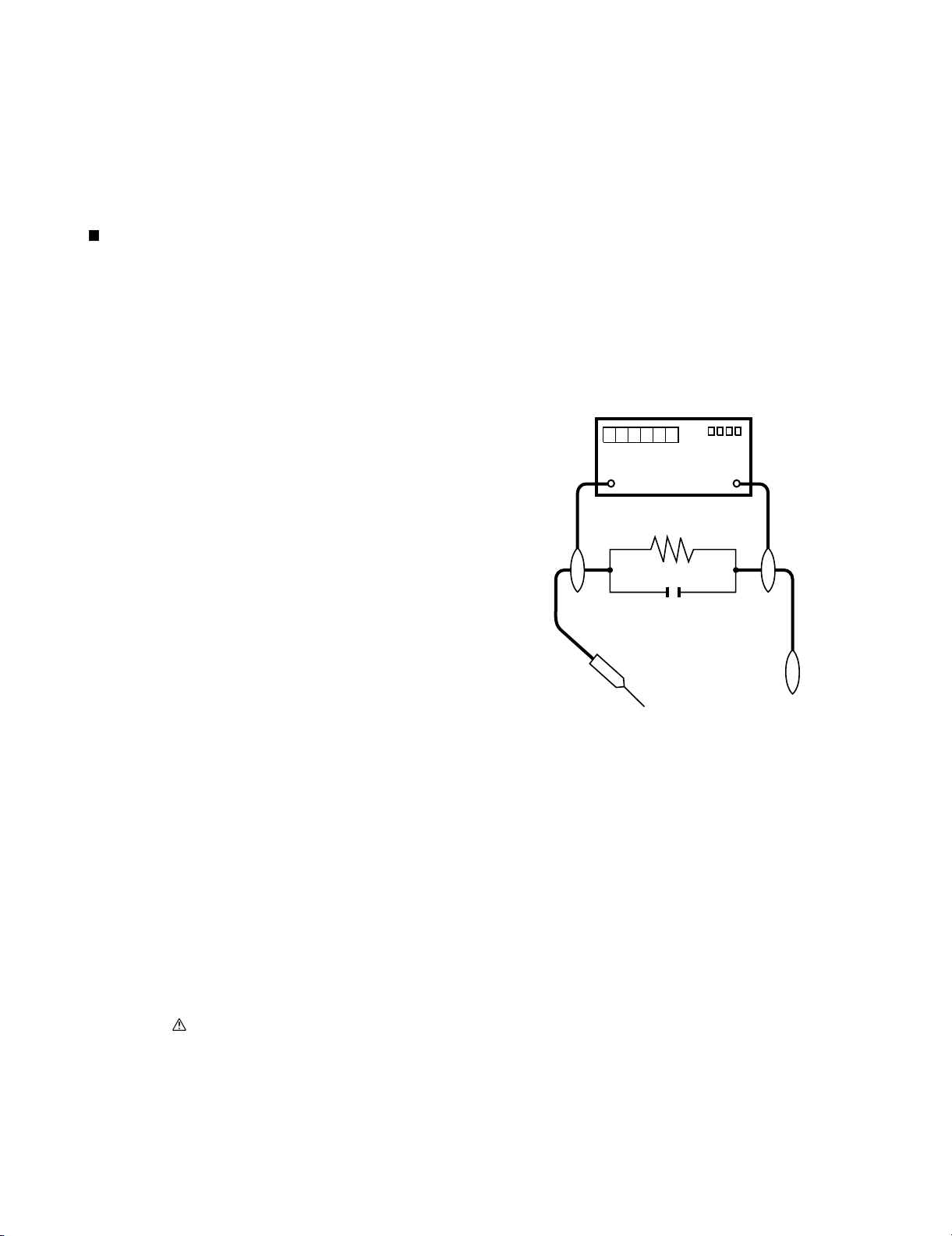
5. To be sure that no shock hazard exists, check for leakage current in
the following manner.
• Plug the AC cord directly into a 110-240 volt AC outlet.
• Using two clip leads, connect a 1.5k ohm, 10 watt resistor paralleled by a 0.15 F capacitor in series with all exposed metal cabinet
parts and a known earth ground, such as electrical conduit or electrical ground connected to an earth ground.
• Use an AC voltmeter having with 5000 ohm per volt, or higher, sensitivity or measure the AC voltage drop across the resistor.
• Connect the resistor connection to all exposed metal parts having a
return to the chassis (antenna, metal cabinet, screw heads, knobs
and control shafts, escutcheon, etc.) and measure the AC voltage
drop across the resistor.
///////////////////////////////////////////////////////////////////////////////////////////////////////////////////////////////////////////////////////////////////////////////////////////////////////////////////////////////////////////
TO EXPOSED
METAL PARTS
DVM
AC SCALE
1.5k ohm
10W
0.15µF
TEST PROBE
CONNECT TO
KNOWN EARTH
GROUND
SAFETY NOTICE
Many electrical and mechanical parts in LCD colour television have
special safety-related characteristics.
These characteristics are often not evident from visual inspection, nor
can pr otection afforded by them be necessarily increased by using
replacement components rated for higher voltage, wattage, etc.
Replacement parts which have these special safety characteristics are
identified in this manual; electrical components having such features
are identified by " " and shaded areas in the Replacement Parts List
and Schematic Diagrams.
///////////////////////////////////////////////////////////////////////////////////////////////////////////////////////////////////////////////////////////////////////////////////////////////////////////////////////////////////////////
PRECAUTIONSAFETY PRECAUTIONSAFETY PRECAUTIO NSAFETY PRECAUTIONSAFETY PRECAUTIO NSAFETY PRECAUTIONSAFETY PRECAUTI ON
For continued protection, replacement parts must be identical to those
used in the original circuit.
The use of a substitute replacement parts which do not have the same
safety characteristics as the factory recommended replacement parts
shown in this service manual, may create shock, fire or other hazards.
i
Page 3
LC-39LE155M
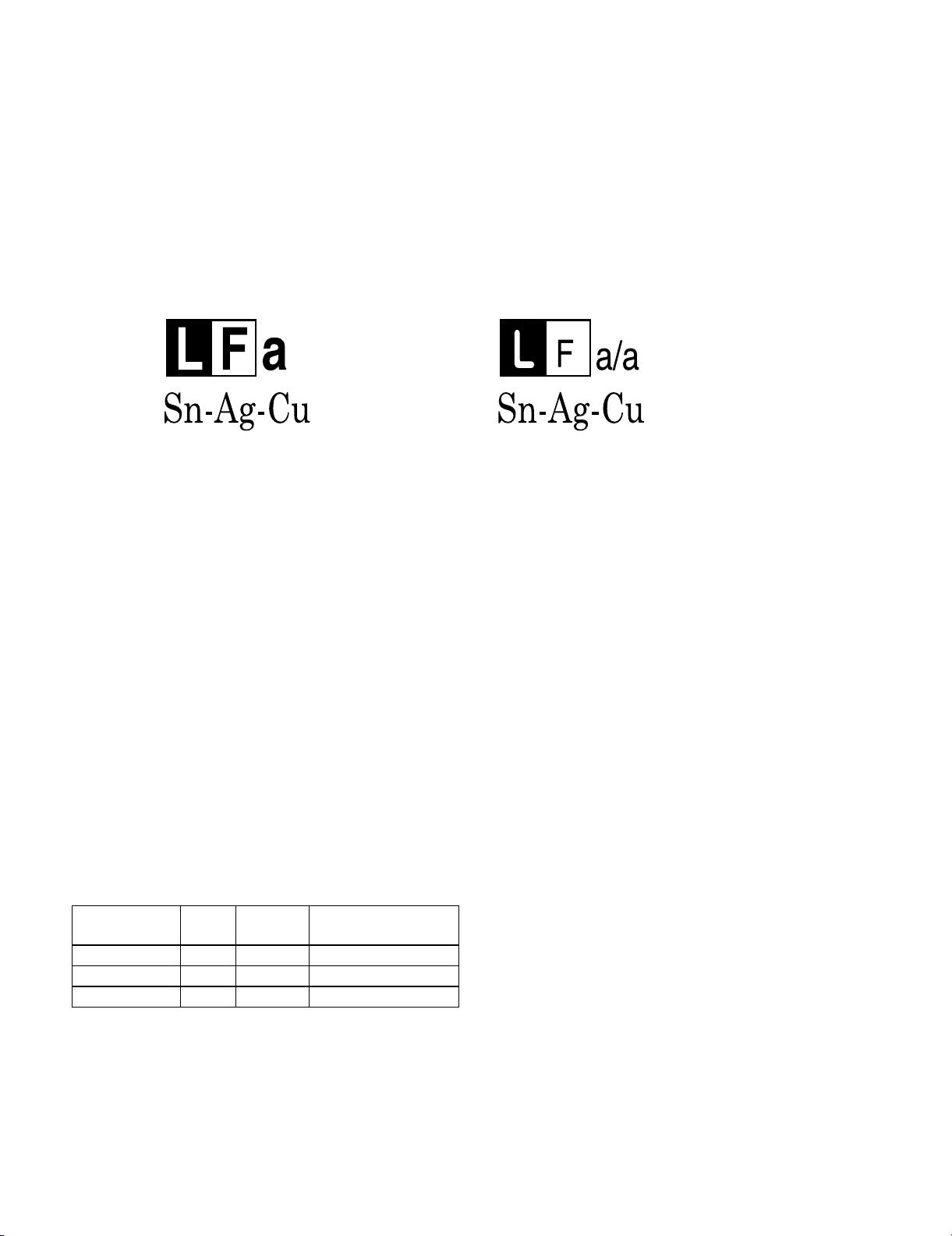
PRECAUTIONS FOR USING LEAD-FREE SOLDER
Employing lead-free solder
• “PWBs” of this model employs lead-free solder. The LF symbol indicates lead-free solder, and is attached on the PWBs and service manuals. The
alphabetical character following LF shows the type of lead-free solder.
Example:
Indicates lead-free solder of tin, silver and copper. Indicates lead-free solder of tin, silver and copper.
Using lead-free wire solder
• When fixing the PWB soldered with the lead-free solder, apply lead-free wire solder. Repairing with conventional lead wire solder may cause damage or accident due to cracks.
As the melting point of lead-free solder (Sn-Ag-Cu) is higher than the lead wire solder by 40 C, we recommend you to use a dedicated soldering
bit, if you are not familiar with how to obtain lead-free wire solder or soldering bit, contact our service station or service branch in your area.
Soldering
• As the melting point of lead-free solder (Sn-Ag-Cu) is about 220 C which is higher than the conventional lead solder by 40 C, and as it has poor
solder wettability, you may be apt to keep the soldering bit in contact with the PWB for extended period of time. However, Since the land may be
peeled off or the maximum heat-resistance temperature of parts may be exceeded, remove the bit from the PWB as soon as you confirm the
steady soldering condition.
Lead-free solder contains more tin, and the end of the soldering bit may be easily corroded. Make sure to turn on and off the power of the bit as
required.
If a different type of solder stays on the tip of the soldering bit, it is alloyed with lead-free solder. Clean the bit after every use of it.
When the tip of the soldering bit is blackened during use, file it with steel wool or fine sandpaper.
• Be careful when replacing parts with polarity indication on the PWB silk.
Lead-free wire solder for servicing
PARTS CODE
ZHNDAi123250E BL J 0.3mm 250g (1roll)
ZHNDAi126500E BK J 0.6mm 500g (1roll)
ZHNDAi12801KE BM J 1.0mm 1kg (1roll)
PRICE
RANK
PART
DELIVERY
DESCRIPTION
ii
Page 4
LC-39LE155M
)
CHAPTER 1. OUTLINE
[1] OUTLINE
[1]
OUTLINE
MAJOR SERVICEPA
PWB
UNIT
Ref No.PartN
N
N
N
DKEYMG311FM01
RDENCA470WJPZ
DUNTKG238FM03
o
.Des
RTS
MAIN Unit
POWER Unit
LED RC Unit
OTHER UNIT
Ref N
o.
N
N
N
Part No. D
RLCDTA296WJQZ
CLCDTA318WE01
RUNTKB187WJZZ
LCD Hiraki Panel Unit
LCD Panel Module Unit
LED BAR (A)
criptio
n
escription
N
RUNTKB188WJZZ
LED BAR(B
1 – 1
Page 5
CHAPTER 2. SPECIFICATIONS
[1] SPECIFICATIONS
Specifications
LC-39LE155M
Item
Screen size
Resolution
Video Colour System PAL/SECAM/NTSC 3.58/NTSC 4.43/PAL 60
TV
Function
Audio amplifier/Speakers
Terminals
OSD language
Power Requirement AC 110—240 V, 50/60 Hz
Power Consumption 57 W (1.0 W Stand by )
Dimensions
Operating Temperature 0°C — 40°C
TV-Standard
Receiving
Channel
TV-Tuning System Auto Preset 99 ch
STEREO/BILINGUAL NICAM: B/G, I, D/K A2 stereo: B/G
Antenna input
INPUT 1 HDMI (HDMI input), PC input
INPUT 2 VIDEO in, AUDIO in, COMPONENT in
INPUT 3 VIDEO in, AUDIO in
OUTPUT AUDIO out, Headphone (
without stand
with stand
Model
CATV
mc89
073,600 pixels (1920 g 1080)
PAL: B/G, D/K, I SECAM: B/G, D/K, K/K
FHU/FHV
S1—S41ch (including Hyperband)
5 W g 2 / 3 g 10 cm 2pcs
UHF/VHF 75 q DIN type
English/Simplified Chinese/Arabic/French/Portuguese/Russian/Persian/Thai/
Vietnamese/Indonesian
898 (W) g 553 (H) g 81 (D) mm
898 (W) g 633 (H) g 236 (D) mm
M551EL93-CL
zHM52.368—52.44
º671:Vº671:HselgnagniweiV
3.5 mm stereo)
1
NTSC: M
)dnatshtiw(gk0.7/)dnatstuohtiw(gk3.6thgieW
s As a part of policy of continuous improvement, SHARP reserves the right to make design and specification changes for
product improvement without prior notice. The performance specification figures indicated are nominal values of production
units. There may be some deviations from these values in individual units.
2 – 1
Page 6
LC-39LE155M
CHAPTER 3. OPERATION MANUAL
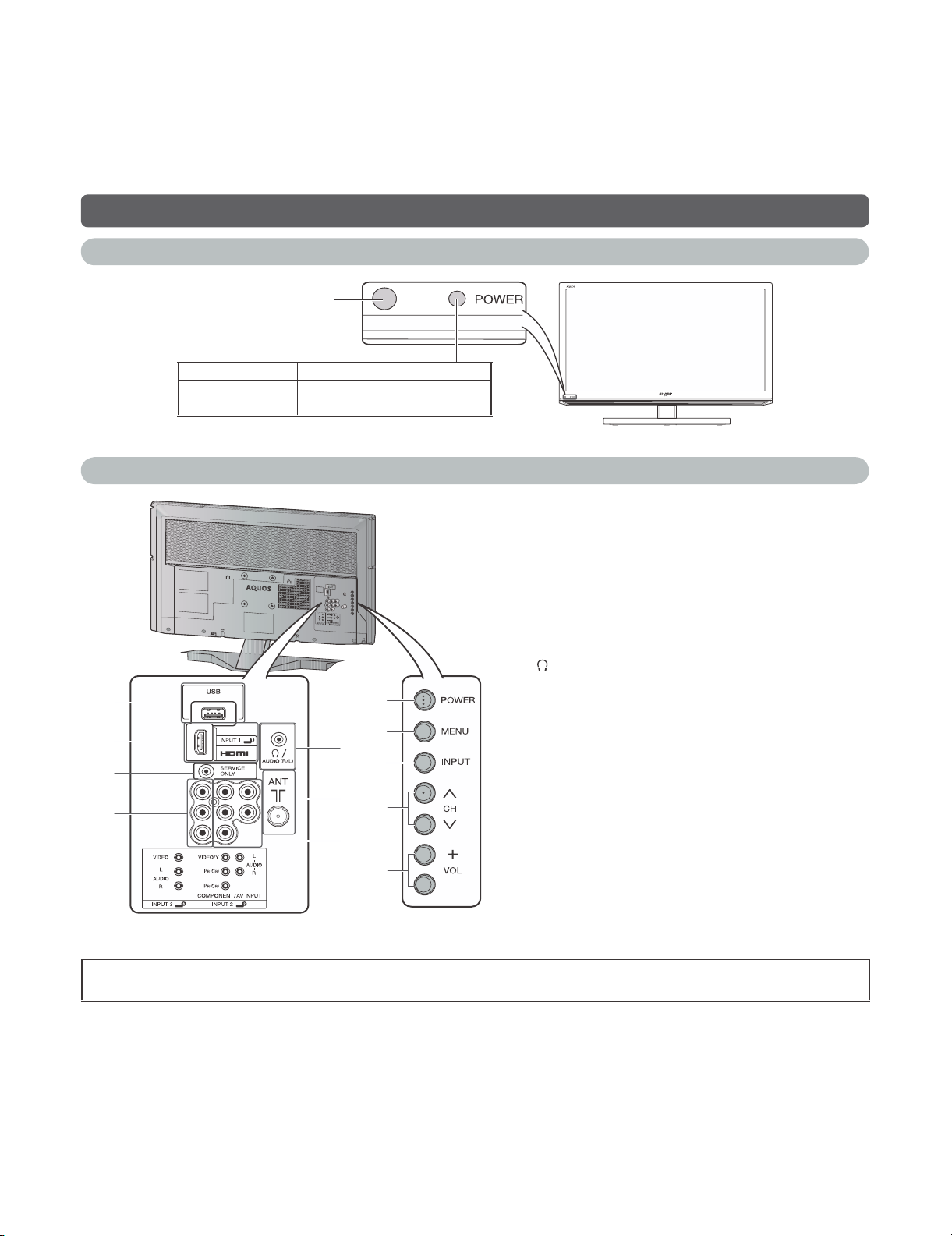
[1] OPERATION MANUAL
Part names
TV (Front)
Remote control sensor
POWER indicator
Light off Power off.
Lighted (Red) The TV is in standby mode.
Lighted (Green) The TV is on.
TV (Rear)
1 POWER (On/Off) button
2 MENU button
3 INPUT button
4 Channel up (r)/down (
5 Volume up (e)/down (f) buttons
6 USB terminal*
7 INPUT 1 (HDMI) terminal
8 SERVICE ONLY terminal**
9 INPUT 3 terminals
10
/AUDIO output (R/L) terminal
11 Antenna input terminal
12 INPUT 2 (COMPONENT/AV INPUT) terminals
10
11
12
1
2
3
4
5
6
7
8
9
* USB terminal use for USB Media Player.
** Usually do not connect anything to this terminal as it is reserved only for service personnel.
s The illustrations in this operation manual are for explanation purposes and may vary slightly from the actual operations.
s The illustrations used throughout this manual are based on LC-32LE155M.
s
) buttons
3 – 1
Page 7
Remote control unit
LC-39LE155M
12
13
14
15
16
17
18
19
10
11
1
2
3
4
5
6
7
8
9
TIMER
1 POWER (STANDBY/ON)
To switch the power on and off.
2 DISPLAY
Display the channel or input information.
3 TIMER
Set the Sleep Timer and Reminder.
4 0 – 9
Set the channel.
5A (Flashback)
PressA to return to the previous selected channel
or external input mode.
6 AV MODE
Select an audio and video setting.
7 VOLk/VOL
l
Set the volume.
(VOLk) Increase the volume.
(VOLl) Decrease the volume.
8e (Mute)
e s
Press
Mutes sound.
Presse again s Restores sound.
Mute will be cancelled after 30 minutes. However, the TV
will not suddenly output loud sound as the volume level will
be set to 0 automatically. Increase the volume level by
pressing VOLk.
9a/b/c/d (Cursor)
Select a desired item on the setting screen.
ENTER
Execute a command.
10 WIDE
Change the wide image mode.
11 Colour (Red/Green/Yellow/Blue)
The coloured buttons are correspondingly used to select the
coloured items on the screen.
12 ECO
Reduce overall power consumption based on user
preferences.
13 COLOUR ADJ. (FREEZE)
Freeze a motion picture on the screen and adjust the colour
tone of the still image.
14 PHOTO
Display your pictures directly on the TV screen.
15 INPUT (INPUT SOURCE)
Select an input source.
16 CHr/CH
s
TV input mode: Select the channel.
(CHr) Increase the channel number.
s
(CH
) Decrease the channel number.
17 MENU
Display the menu screen.
18 MPX
Select the sound multiplex mode.
19 RETURN
MENU mode: Return to the previous menu screen.
3 – 2
Page 8
LC-39LE155M
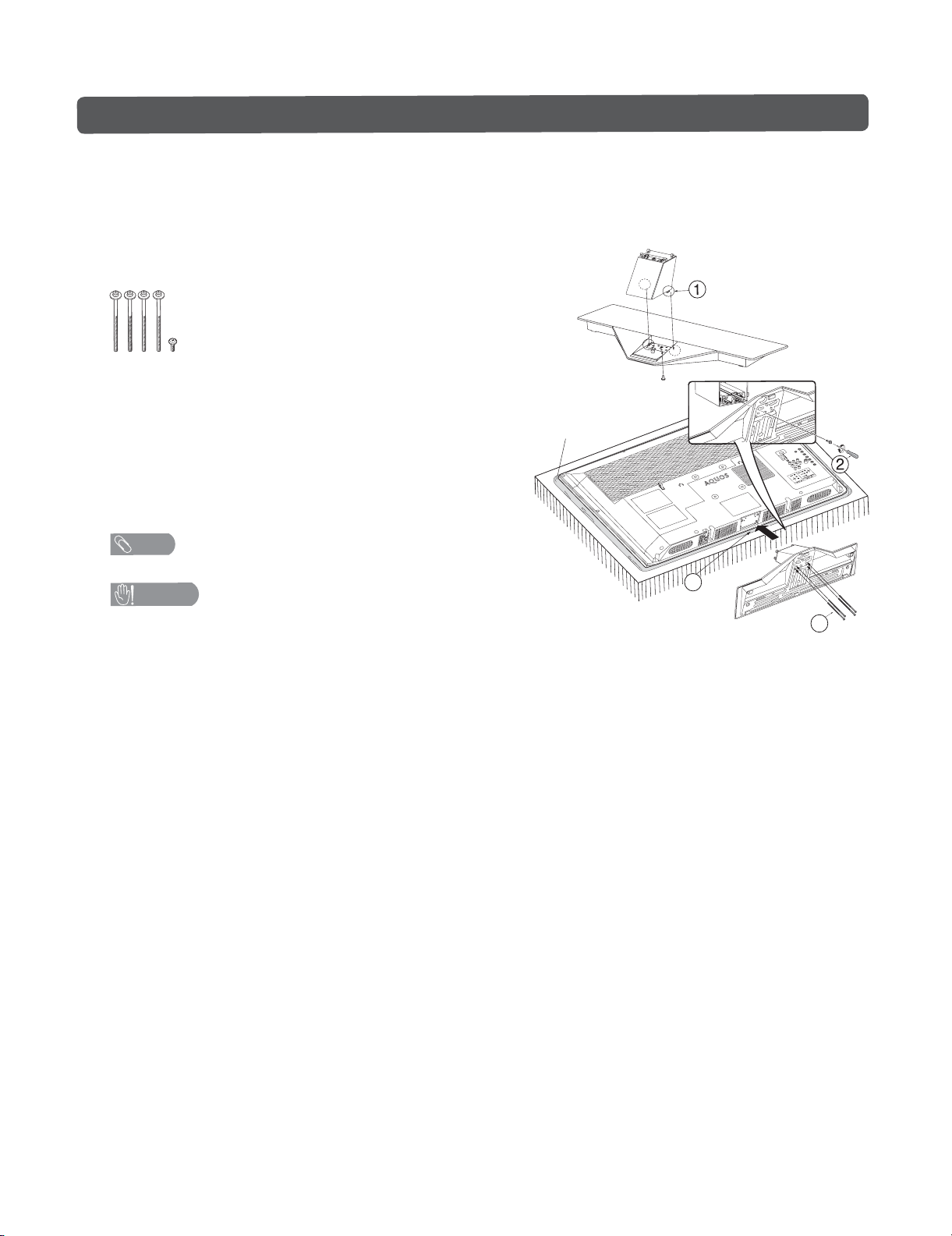
Attaching the stand
• Before attaching (or detaching) the stand, unplug the AC cord from the AC outlet.
he TV on. This will prevent it from
• Before performing work spread cushioning over the base area to lay
being damaged.
Con-rm the screws supplied with the TV.
t
Screws (
(used in step 2 and 3)
m
5)
Insert and hook post guide into stand base slot
holes. (
Fix the post using short screw. (
1
)
)
2
Insert the stand basetothe
bottom of the TV. (
3
)
Insert and tighten the 4 long screws into the 4
)
holes on the bottom of the stand base. (
NOTE
• To deta
• Do not attach or detach the stand without holding it.
Doing so can cause the stand to fall, resulting in serious
personal injuries as well as damage to the stand.
ch the s
CAUTION
tand, perform the ste
4
in reverse order.
s
p
Soft cushion
3
4
3 – 3
Page 9
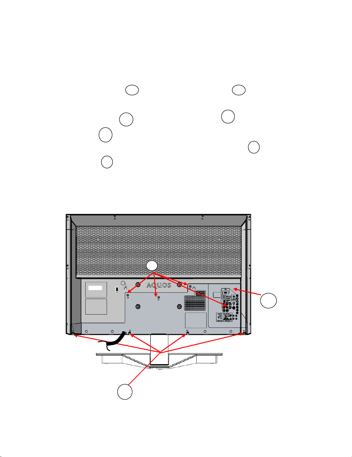
CHAPTER 4. REMOVING OF MAJOR
PARTS
[1] REMOVING MAJOR PARTS
LC-39LE155M
1.Remove the 8 screws
and slowly pull out to the right . ( Refer figure .1 )
2.Disconnect LED BL Wire and disconnect PD Wire . ( Refer figure 2)
3.Remove 4 screws from power board.
5
4.For remove main unit disconnect LVDS wire ,IR wire & speaker wire
and remove 1 screw at main unit.(Referfigure2)
Figure 1
7
1 2
and detach bottom cover by pull up bottom area
3
4
6
1
2
1
4 – 1
Page 10
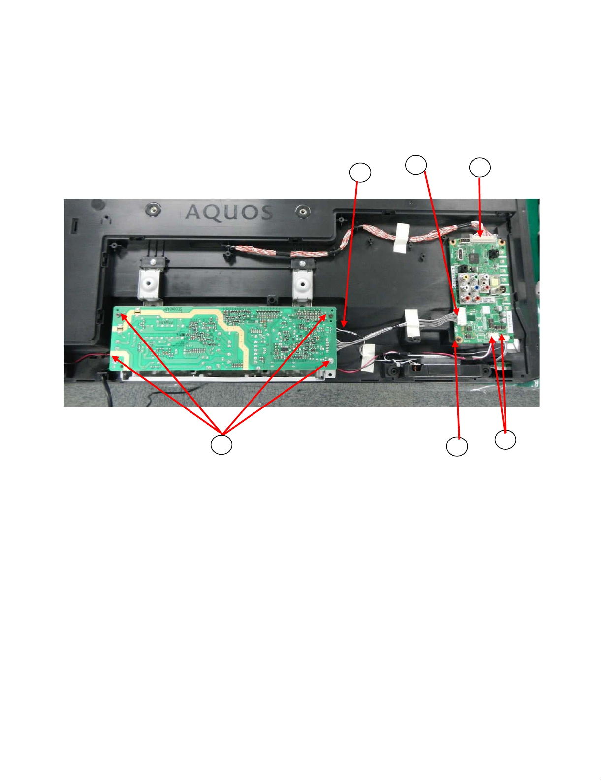
LC-39LE155M
Figure 2
3
5
4
6
7
6
4 – 2
Page 11
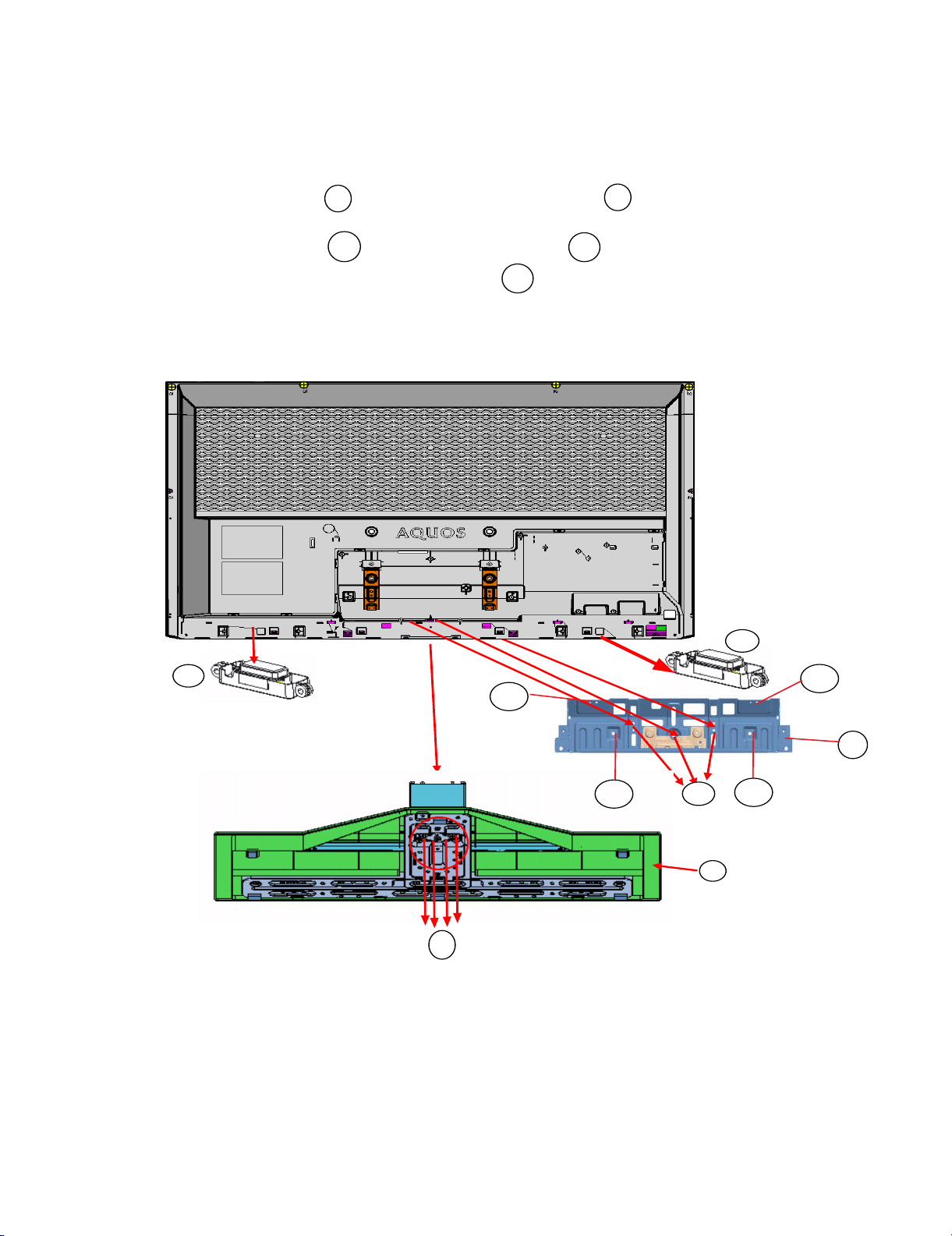
[2] REMOVING OF STAND ASSEMBLY & BOTTOM
BRACKET & SPEAKER L/R
LC-39LE155M
1.Remove 4 screws and detach the stand assembly
2.Remove 7 screws and detach bottom bracket .
3.Remove the speaker L/R from rear cabinet
1
3
4
5
2
5
5
3
3
3
3
2
3
4
1
4 – 3
Page 12
LC-39LE155M
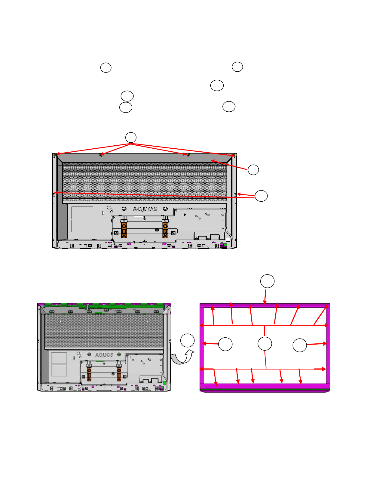
[3] REMOVING OF THE LCD PANEL MODULE
1.Remove 4 screws and detach top cover by unhook 7 hooks
2.Unhook 5 hooks that attach to bezel and remove 2 screws .
3.Then turn the set to front
4.Detach the front cabinet by unhook remaining 10 hooks .
1
3
4
5
1
6
2
2
3
5
4
6
6
6
4 – 4
Page 13
CHAPTER 5. ADJUSTMENT
[1] ADJUSTMENT
[1]
ADJUSTMENT PROCEDURE
1.
Entering
1) While holding down the
inspec-
2) Press the Channel DOWN and Volume DOWN keys at the same time. (The
3) To cancel
2.
Remote controller
1. key
and
cancel the adjustment process mode
INPUT
tion process m ode is
it, turn off the power using the Power switch or remote
operation
and Volume DOWN keys at t he same time, plug in the AC cord to turn on the power. (“K” standing for
displayed
key
on the upper left position of the
operation
and
description of display in adjustment process mode.
control.
screen.)
adjustment
process mode screen
LC-39LE155M
appears.)
Remote controller key
CH ( /
VOL (+ /
Cursor ( /
Cursor ( /
INPUT button on
controller
ENTER —————— ——————
* Input mode is switched
3.
Software upgrading.
1) Plug off the LCD
)
–)
)
)
remote
CH ( /
VOL (+ /
——————
——————
INPUT
automatically
TV.
2) Insert the USB device to the USB terminal at the LCD
(Make sure that the latest software is installed in the USB
3) Hold the LCD TV power key and plug on the LCD
4) LCD TV is on and detecting the USB
5) A few
seconds later, L E D l i g h t ( o r a n g e ) wi l l b l i n k i n d i c a t i n g the software
Main
–)
button
when relevant
unit key
)
device.
adjustment
Changing
Changing
Turning a page
Changing
Input source switching (toggle
(ATV IN PUT1 INPUT2 INPUT3
is started so far as the
selected line
selected line setting
(PREVIOUS/NEXT)
a selected line setting
necessary
TV.
device).
TV.
F
(UP/DOWN)
(+1/-1)
(+10/-10)
switching)
input signal is
unction
)
available.
upgrading.
7) T V w i l l a u t o m a t i c a l l y r e s t a r t w h e n s oftware is successfully installed
8) LCD TV is running with the latest software.
5 – 1
Page 14
LC-39LE155M
Adjust the VCOM value by volume resistor (VR)
Revolve the VR till the f licker bec omes the
4.
EDID DATA
No need to i nput
INPUT
EDID
5. VCOM ADJUSTMENT
a. Setting [Signal]
b. Manual VCOM
adjustment
6. SIGNAL ADJUSTMENT
6.1 PICTURE ADJUSTMENT
Confirmation of signal from generator (sett ing to spec level)
PAL Composite signal :0.7Vp-p ± 0.02Vp-p (pedestal to white level)
15K Component signal (50Hz) :Ylevel :0.7Vp-p ± 0.02Vp-p (pedestal to white level)
33K Component signal :Ylevel :0.7Vp-p ± 0.02Vp-p (pedestal to white level)
6.1.1 Adjustment Mode
1 Adjustment Mode Press the test key at the test remote control
6.1.2 Component 15K 50Hz Signal A djustment (COMP-SD)
1
Setting
ITEM CONDITION PROCEDURE
Flicker pattern
(2H checkered
pattern (2n+1))
LEVEL ½ MAX
With Hiraki panel
condition
Pb, Pr l evel :0.7Vp-p :0.7Vp- p ± 0.02Vp-p
Pb, Pr l evel :0.7Vp-p :0.7Vp- p ± 0.02Vp-Com
ITEM CONDIT
ITEM CONDITION PROCEDURE
[Signal]
COMP 15K 50Hz
(576i)
100% Full-field
Colour Bar
[Terminal]
COMPONENT
INPUT 2
ION PROCEDURE
・Input flicker pattern
RGB 2H+1 checkered pattern
1.
on
SC-PWB with screw driver.
2.
weake st.
・Feed the COMPONENT 15K 50Hz (576i) 100% Full-field
Colour Bar signal(100% colour saturation) to
COMPONENT INPUT 2
100% White
→←
Black
2 Auto Adjustment Test Mode page 4
(COMP SD)
At the r elated page, m ove cursor to [ COMP SD A DJ], press
ENTER.
[OK] appears when finished.
6.1.3 Component 33K 60Hz Signal Adjustment (COMP-HD)
ITEM CONDITION PROCEDURE
1
Setting
[Signal]
COMP 33K 60Hz
(1080i)
100% Full-field
・Feed the COMPONENT 33K 60Hz (1080i) 100% Full-field
Colour Bar signal(100% colour saturation) to
COMPONENT INPUT2
Colour Bar
[Terminal]
COMPONENT
100% White
INPUT 2
2 Auto Adjustment Test Mode page 5
(COMP HD)
At the related page, move cursor to [COMP HD ADJ], press
ENTER.
[OK] appears when finished.
→←
Black
5 – 2
Page 15
6.2) White Balance Adjustment
T
T
N
O. ITEM CONDITION PROCEDURE
LC-39LE155M
1 Setting Backlight : MAX
AV Mode : DYNAMIC
Active Backlight :
OFF
Set the luminance
meter on the centre
of the screen
2Auto
Initial setting Panel Contrast
Adjustment
[command]
Adjustment
Mode
KRSW0001
KKT10037
Setting
KYOF0001
OSDS0001
SBSL0016
Multi point
adj. Mode
MSET0000
WBI20255
Point 2
WBI20204
MG2G****
MG2B****
MG2R****
Point 1
WBI10051
MG1G****
MG1B****
MG1R****
(1) Measurement MAX Brightness
(2) Set MIN Brightness
(3) Measurement HIGH Brightness
(4) Measurement LOW Bri ghtness
(5) Calculation H γ
(6) Calculation Lγ
(7) Calculation HIGH luminance (γ=2.2)
(8) Calculation Initial setting of R/G/B_HIGH
(9) Set Initial setting of R/G/B_HIGH
(10) Original WB adjustment is performed (HIGH)
Set the specified gradation for poin
most faint colour to get reference value,
adjust others 2 colours to minus adjustment for
reference value of point 2.
(11) Measurement HIGH Brightness
(Set) R_HIGH= G_HIGH
(12) Calculation MAX luminance after WB
(13) Set R/G/B_MAX
For the details of white balance adjustment procedure, please refer to white
balance
adjustment spec for Kameyama model.
1. Confirm the set condition.
2. Connect the white balance jig.
3. Through RS-232C command, adjustment mode screen is displayed.
R/G/B_MAX
R/G/B_HIGH
R/G/B_LOW
G_HIGH= G_HIGH
B_HIGH= G_HIGH
ADJ set to γ=2.2(L
XHG
t2,fixthe
)
C
nt
=3000:1
WB
MAX
= 4080
WB
H
= 3664/4080
WB
L
= 1008/4080
L
max
=305.7 cd/m²
min=Lmax/Cnt
L
XH
=235.1 cd/m²
L
XL
=2.06 cd/m²
L
HX
=(L
H
/WB
=WB
XH
H
/WB
XL
L
/WB
max-Lmin
MAX
MAX
Hγ=LOG((L
LOG(WB
Lγ=LOG((L
LOG(WB
H22
L
(WB
WB
(1/H γ)=3703
R_HIGH=WB
G_HIGH=WB
B_HIGH=WB
R_HIGH=3702
G_HIGH=3641
B_HIGH=3703
R_HIGH=3641
G_HIGH=3641
B_HIGH=3641
XMX=LXHG
L
/((W
=0.102
-L
min
MAX
)= 2.44
-L
min
MAX
)=2.73
)x
)^2.2+L
X ((L
HX
’=3703
HX
’=3703
HX
’=3703
B
H
/WB
Example: G6 panel also us e
for G8/ CSOT, C MI (b e car eful
of INT s ett ing)
)/(L
)/(L
min
H22
max-Lmin
max-Lmin
=241.31
-L
min
))/
))/
)/(L
max-Lmin
RESUL
L
XHG
=231.3
MAX
)^2.2)=293.04
))^
Write
MSET0003
Set
Max.Level
MGMG****
MGMR****
MGMB****
(14) Calculation LOW luminanc
(15) Calculation Initial setting of R/G/B_LOW
(16) Set Initial setting of R/G/B_LOW
(17) Original WB adjustment is performed (LOW).
Set the specified gradation for point 1. Set G of
e(γ=2.2)
R_MAX=G_MAX*(R_HIGH/G_HIGH)=4078
MAX
X((L
XMX
-L
min
)/(L
max
G_MAX=WB
min
))^(1/Hγ)=4010
L
-
B_MAX=G_MAX*(B_HIGH/G_HIGH)=4078
XLX
=(L
XMX
-L
min
L
LX
=WB
WB
min
))^(1/Lγ)=901
L
MAX
X ((L
)x(WBL/WB
XLX
MAX
)^2.2+L
-L
min
)/(L
max
min
-
=5.08
point 1 to the default value [(R1 x G value of
point 2/R2), wit h fractions rounded] and adjust
RB to the reference value of point 1.
R_LOW=WB
G_LOW=WB
B_LOW=WB
XLX
XLX
XLX
=901
=901
=901
RESUL
R_LOW= 921
(18) Adjusted value is writing at [command]
MSET0003
(19) Set the G of point Max. to
the default value
5 – 3
G_LOW=901
B_LOW=971
Page 16

LC-39LE155M
(4080 x G value of point 2 / R2). Set the R,B
Max. value [G
value of point 2)
(20) Calcul ate the sl ope R2
between MAX and Point2. R2
(R
max-Rhigh
(21) Calcul ate the c orrecti on val ue ⊿R
⊿G
high,⊿Bhigh.
(3840-3664)
(22)
Set the reference value R,G,B of point 2
(R2’)=R2+⊿R
(23)
Calculate the slope R1
between Point2 and Point 1. R1
(R
high-Rlow
(24)
Calculate the correction value ⊿R
⊿G
low,⊿Blow.
⊿R
low =R1slope X
Set the reference value R,G,B of point 1
(25)
(R1’)=R1+⊿R
(26) Shut down the AC power.
※Initia l value at RG B 2 poi nt : 3664
※Initial value at RGB 1 point : 1008
[Adju stment valu e]
☆Teachi ng set send b y engineeri ng dep t is set a s
nce.
refere
[Refer ence val ues for adjustm ent ref erence]
Equipm ent : Lumi nance meter [ Minolt a CA-210]
Point
2ref.
values
Point
1ref.
values
Ref. : F or inspectio n, set th e LCD TV as bel ow.
Level
229
63
AV MODE : [DYNAMIC] (Reset)
Aging Time : Minimum 5 minutes
– G value of point 2 + (R,B
max
slope,G2slope,B2slope
)/(4080-3664)
⊿R
high
slope,G1slope,B1slope
)/(3664-1008)
(1130-1008)
low
Spec
Data
x=0.270
y=0.265
x=0.270
y=0.265
Adjustment
Spec.
0.0010 0.0020
0.0045 0.0090
slope =
high,
high =R2slope X
slope =
low,
Inspection
Spec.
7. FACTORY SETTING
AC power is plug off af ter shipment setting is done.
Caution: Do not plug on again after shipment setting is done. If do, please re-do the shipment setting. Do
not off with remote control.
ITEM CONDITION PROCEDURE
Factory setting AC power off to exit
the factory setting.
1. Setting is done with test remote control.
2. Press the ‘Factory Setting’ key on the remote control
continuously.
3. When Green background appears on screen and ‘K’ mark
disappears, seƫng is completed.
The followings are initialised to f actory setting
1) User setting
2) Channel data (e.g. broadcast frequencies)
3) Manufacturer’s option settings
4) Password data
5) Setting val ues are set based on model desti nation
Model Name Factory Setting Key
A3KLX1WVZ/J/I/Y/B/N/M
A3KLX1WVP
Name
M-Setting 10000000101011 0 B/G ENGLISH
P-Setting 100000001011110 M ENGLISH
Remote Control
Code
S-System Setting OSD Language
**Please do inspection f or A3KLX1WVP using NTSC signal.
Setting
5 – 4
Page 17

CHAPTER 6. TROUBLESHOOTING
TABLE
[1] TROUBLESHOOTING TABLE
[1] TROUBLESHOOTING TABLE
No power (front LED failure to light up) or no startup (front LED failure to turn from red to green)
LC-39LE155M
Are the wire harnesses and other cables properly connected in
the set?
YES
Is there the AC_CTRL and PNL_POWER signal input at pins
(126) and (127) of IC3301?
YES
Are the DC/DC converter outputs and the output voltages along
the control lines as specified?
1) M+5.6V (IC9603)
2) D+1.26V (IC9605)
3) D+5V (IC9610)
4) T+5V (IC9612)
5) D+3.3V (IC9608)
6) D+1.8V (IC9609)
7) D+2.5V (IC9611)
NO Reconnect the wire harnesses and other cables properly in the
set.
NO Check the AC_CTRL signal line PNL_POWER signal line.
NO Check the DC/DC converters and the control lines. Replace
defective parts as required.
6 – 1
Page 18

LC-39LE155M
With [RF] signal input No video onscreen (1)
No video in the UHF/VHF reception
Is there IF output from the tuner pin(10) of TU1101 as specified? NO Check TU1101 and its peripheral circuits.
YES
Is there VIF input at pin 74 & 75 of IC3301? NO Check the circuit between TU1101 & IC3301.
YES
Are there the signal outputs (pin 100-107, 109,110) of IC3301? NO Check IC3301 and its peripheral circuit.
YES
Check LVDS cable, LCD controller (incl. panel) and their peripheral circuits.
With <Video> signal input No video onscreen (2)
No external input video onscreen <INPUT 2>
Is INPUT 2 selected on the input select menu screen? NO Select INPUT 2 on the input select menu screen to pick up the
right input signal.
YES
Is there the video signal input at pin (43) of IC3301? NO Check the line between pin (9) of J502 and pin (43) of IC3301.
YES
Are there the signal outputs (pin 100-107, 109,110) of IC3301? NO Check IC3301 and its peripheral circuits.
YES
Check LVDS cable, LCD controller (incl. panel) and their peripheral circuits.
6 – 2
Page 19

LC-39LE155M
With <Component> signal input No video onscreen (3)
No exter nal input video onscreen <INPUT 3>
Is INPUT 3 selected on the input select menu screen? NO Select INPUT 3 on the input select menu screen to pick up the
right input signal.
YES
Are there the Y, Pb and Pr signal inputs at pins (34), (36) and
(38) of IC3301 respectively?
YES
Are there the signal outputs (pin 100-107, 109,110) of IC3301? NO Check IC3301 and its peripheral circuits.
YES
Check LVDS cable, LCD controller (incl. panel) and their periph-
eral circuits.
NO Check the line between pins (19)/(17)/(15) of J502 and pins (34)/
(36)/(38) of IC3301.
With <HDMI> signal input No vi deo onscreen (4)
No exter nal input video onscreen <INPUT 1>.
Is INPUT 1 selected on the menu screen? NO Select INPUT 1 on the input select menu screen to pick up the
right signal input.
YES
Are there signal outputs from SC1501 to IC3301? NO Check peripheral circuits between SC1501 and IC3301.
YES
Are there the signal outputs (pin 100-107, 109,110) of IC3301? NO Check IC3301 and its peripheral circuits.
YES
Check LVDS cable, LCD controller (incl. panel) and their peripheral circuits.
6 – 3
Page 20

LC-39LE155M
No sound in the UHF/VHF reception.
No audio heard (1)
Is the IF output from the tuner pin (8),(9)
of TU1101 as specified?
NO Check TU1101 and its peripheral circuits.
YES
Is there the SIF signal input at pins (R6 ), (T6 ) of IC3301? NO Check IC3301 and its peripheral circuits.
YES
Is there audio signal intput at pin(4),(10) of IC1701? NO Check connection between IC3301 and IC1701 and its
peripheral circuits.
YES
Is the L-ch audio signal output at pin((27), (29) of IC1701 normal? NO Check IC1701 and its peripheral circuits.
Is the R-ch audio signal output at pin(21), (23) of IC1701 normal?
YES
Are the audio signal L-ch and R-ch output at (3)/(4) and (1)/(2) of
P1701 normal?
YES
Check speakers and their peripheral circuits.
NO Check circuit between IC1701 & P1701.
6 – 4
Page 21

No audio heard (2)
No external audio heard
<INPUT 2>
Is there the L-ch audio signal input from pin (2) of input terminal
J506 to pin (N2 ) of IC 3301?
Is there the R-ch audio signal input from pin (4) of input terminal
J506 to pin (P1) of IC 3301?
<INPUT 3>
Is there the L-ch audio signal input from pin (8) of input terminal
J502 to pin (M 2) of IC3301?
Is there the R-ch audio signal input from pin (9) of input terminal
J502 to pin (N1) of IC 3301?
LC-39LE155M
YES
Is there the I2S signal output at pin (B14) (C14) of IC3301? NO Check IC3301 and its peripheral circuits.
YES
Is there audio signal inp ut at pin(4),(10) of IC1701? NO Check connection between IC3301 and IC1701 and its periph-
eral circuits.
YES
Is the L-ch audio signal output at pin(27), (29 ) of
1701 normal?
IC
NO Check IC1701 and its peripheral circuits.
Is the R- ch audio signal output at pin(21), (23) of IC1701 normal?
YES
Are the audio signal L-ch and R-ch output at (3)/(4) and (1)/(2) of
NO Check circuit between IC1701 & P1701.
P1701 normal?
YES
Check speakers and their peripheral circuits.
6 – 5
Page 22

LC-39LE155M
No audio heard (3)
No HDMI sound heard. <INPUT 1>
(*INPUT 1 is digital audio.)
Does the HDMI image appear onscreen? NO Refer to “<INPUT 1> in No external input video onscreen
(HDMI)”.
YES
No audio output from <IN PUT 1> NO Check it if EDID is written or not.
YES
Are waveforms input in to the pin A2,A3,B2,B3,B1,C3,C1,C2,
NO Check peripheral circuits IC3301.
of IC3301 normally?
YES
Is there audio signal input at pin(4),(10) of IC1701? NO Check connection between IC3301 and IC1701 and its periph-
eral circuits.
YES
Is the L-ch audio signal output at pin(27), (29 ) of IC1701 normal? NO Check IC1701 and its peripheral circuits.
Is the R-ch audio signal output at pin(21), (23) of IC1701 normal?
YES
Are the audio signal L-ch and R-ch output at (3)/(4) and (1)/(2) of
NO Check circuit between IC1701 & P1701.
P1701 normal?
YES
Check speakers and their peripheral circuits.
6 – 6
Page 23

CHAPTER 7. OVERALL WIRING /
ࠉࠉࠉࠉ
32"/39"ON
L
Y
ࠉ
ࠉࠉࠉࠉࠉࠉࠉ
MST6120VGM
Ref No.
IC3301
RH-IXD620WJQZQ
L
E
D
D
RI
VE
R
I
C7801
VHI
BD
8779
E
F
-
1
Y
(24" ONL
Y
)
UN
QA
073
W
J
QZ
AUDIOAMP
I
C1701
VHI
T
PA
3130D
-
1Y
I
2C
SP
P
1701
4
p
i
n
S
P
_L
S
T
B
YCT
R
L
TEMP SENSOR
TH3301
L
S
DA
C3
I
M
I
2
C
A
DDR
E
S
S
䠖C
0
MAIN
UART J
A
CK
J501
QJ
AKJA
027WJZ
Z
UAR
T
AUDIO_OUT
0
L
/0R
S
P
I
S
PI I
F
S
P
I
FLA
S
H
WRI
T
E
S
P
_R
S
P
_L
S
P
_R
S
P
_R
㻤䃈5W
IF
MAT
CH
I
NG
CI
R
CUI
T
HDMI 1
S
C1501
QS
OCZ
A271WJ
QZ
Y
I
NP
UT
1
HD
MI
I
N1
H
DMI
DD
C1
S
P
I
FLA
S
H
I
C3101
32K
Bi
t
S
P
_L
㻤䃈㻌5W
US
B
J506
QS
OCZ
A
330WJ
QZ
U
S
B
I
F
XTAL(24MHz)
X3301
RCRSCA239WJQZY
I
NP
UT
2_Y/
CVB
S
,
P
b
,
P
CVB
S
1/
R
I
N1P,
B
IN1P
,
G
I
N1P,
S
OGI
N1
I
N
PUT2
L
/R
CVB
S
0
AUL
0
,
A
UR0
I
P
S
P
_L
S
P
_R
ORCHID II 32/39LE155M
BLOCK DIAGRAM
P
OWE
R
UN
I
T
D
ATA A(8)
C
L
K
A
(2)
PA
NEL
32"WXGA
/
39"FHD
5
0/60H
z
L
VDS
32":
8b
i
t
39":
8
b
i
t
CL
K
A(2)
DATA A
(8)
I
R
I
n
terf
a
ce
P
L
S
C7801
12pi
n
OF
L
BL
_E
RR
12.
2V
CONTROL SW
S101 ~ S107
I
N
P
U
T
2
C
OMPON
E
N
T
/
A
U
D
I
O
I
N
I
N
P
U
T
3
C
V
B
S
/AU
D
I
O
I
N
P
NL
12V
S
T
B
HOT
P
L
UG
A
C
I
5
V
SWI
T
CH
+5.
0V
+3.
30V
K
EY0
L
S
ADC
0/1
GP
I
O
I
N
P
UT
3_
CV
BS
I
N
P
UT
3
L
/R
BL S
U
PP
L
Y
(32"/39"
ONL
Y
)
BL
S
UP
P
L
Y
(24" ONLY
)
OF
L
L
AMP
E
R
R
BL
_ON
L
W
P
3801
30p
i
n
FFC
S
P
M
U
T
E
H
P
OUT L
/R
HP
AMP
I
C1702
VHI
T
PA6139A-
1Y
UR
+
12
.
2
V
T
O
D
CDCCO
NV
ER
T
ER, TUNER
LDO
.
USB,&
H
PA
M
P
.
HP
J
A
CK
J505
QJ
A
KJA030W
J
QZ
H
P
_
IN
T
RA
NS
I
S
T
OR
S
W
(F
OR
WX
GA
+1
.
25V
GP
I
O25
I
R
R
ec
i
eve
r
R
MC
10
1
L
ED
D
1
5
3/
D
15
2
P
15
1
5
P
I
N
S
LE
D
_
I
RP
W
B
P
101
5
P
I
N
S
I
2C
K
EY1
GP
I
O
POP
NOI
S
E
C
/M
G
P
I
O
4
0
F
ROM CPU
S
T
BY CT
RL
S
T
_GP
I
O_0
+
5
.
0
V
P9601
10p
i
n
X
I
N
/X
OUT
I
F+
I
F
-
I
F_
I
N+
I
F_
I
N-
I
2
C(
H
DM
I
)
cl
k
(2
)
d
a
ta
(4)
H
P
D0_
I
N
F
ROM CPU
S
T
BY
C
T
R
L
H
PM
UTE
LINEOUTL
LI
NEOU
TR
H
P
_
L
HP_
R
GP
IO_20
R/C
RLE
D
&
GLED
+3
.
3
V
+3
.
3V
+2.
5V
+1.
8V
+3.
3V
BLOCK DIAGRAM
[1] SYSTEM BLOCK DIAGRAM
LC-39LE155M
7 – 1
Page 24

LC-39LE155M
CHAPTER 8. PRINTED WIRING
BOARD ASSEMBLIES
[1] MAIN Unit / LED IR Unit
H
MAIN PWB -SIDE A
C1116
J504
J504
USB
FDC2
G
SC1501
HDMI
F
P3301
R3336
7
R1515
Q1502
Q1501
R1514
D1502
19
R1511
D1501
D1503
R1512
R1513
R1519
R1518
R1503
SC1501
R1504
R1505
R1506R1507
R1508
R1509
1
R1510
R3339
R3334
P3301
J3301
SERV
R3337
R1517
Q1503
C3301
R3303
1
R9629
R1501
R1502
R1516
R3306
IC3302
Q3301
R3307
R3308
R3335
R9625
R9621R9622
J3301
R3338
R9623
C9623
P3801
VA512
VA513
R520
R519
R3301
R3304
R3310
R3309
C3302
A
R9624
C9625
FB9602
32
R3813
R3814
R3815
R3816
R3811R3812
C1115
R3312
R3317
C3347
R3342
R3302
R3340
R3341
R3320
IC3301
R3305
R3315
R3319
IC3301
C3318
FB3305
C3334
C3329
R9626
R3323
R3322
C9626
L9603
IC9605
1
C9624
5
C3308
C3312
C3316
IC9605
3
C9631
4
R3314
R3313
R3316
VA502
VA503
P3801
3
J503
1
C3341
P3302
R3325
R3328
R3326
7
R3327
C3342 C3343 C3344
R1114
C504
C501
C505
R504
R506
R507
C506
VA504
VA505
VA506
C3319
C3325
C3305
R3321
R3318
R3311
VA501
HP
R3329
C3345
R3332
C3339
C3346
R3331
X3301
C3340
R3333
C502
R505
C503
C510
C507
C508
R511
R509
R510
C509
VA507
R513
R514
X3301
12
J506
R1734
C1739
C1732
R1717
R1720
C1736
C1741
R1110
Q1704
R1109
C1109
R1742
C3337
C3338
R3324
R3330
C511
R512
C512
VA508
LW
1
1
5
C9618
R9601
IC9603
R3101R3102
4
R9602
R517
C514
C1738
C1740
VA511
5
IC1702
IC9603
C513
VA510
R516
R1736
C1742
4
1
C1743
C1744
IC501
16
FDC3
S101
POWER
R102
S107
MENU
S102S103
INPUT
R104
S101
S102
C9630
J503
VA509
C515
R1737
C1737
8
9
IC501
13
R1739
R1738
R1735
E
W
J506
RED WHITE
TU1101
R
TU1101
D9601
R1111R1112
R1113
CH-UP
R103
CH-DOWN
R1731
S103
S104
S104
S105
SMT
Y
W
YELLOW
WHITE
G
J502
B
BLUE GREEN
D
S105
KEY
P1701
1
ABCDEFGH
C1701
C1731
C1735
L1701
P101
R105
P101
FDC1
6
R101
S106
VOL-DOWN
C1731
C1735
KG311WE
5
R106
VOL-UP
S106
7
8
R7805
L7801
C7805
L9601
C9610
C9632
R
R7804
RED
HAND
R1732
R1733
R1701
3
1
R7803
Q7801
CHECKER
Q7801
0
C1701
C1718
C1729
C1730
C1714
ICT
1
2
3
D7801
C7805
D7801
2
P7801
10
1
P7801
SC7801
C9613
SC7801
TEST3
LED
L1704
L1703
QPWBXG311WJZZ
(QKITPG311WJTX)
1
12
C1720
14
C1721
C1725
C1728
C1724
P1701
SP
L1702
C1712
C1711
C1707
C1708
UL1
54
R
RED
C
J502
1
POW
P9601
L7801
P9601
B
A
1
UR1
10
R9620
R9603
R9628
C9608
a
LF1
R9609
C9606
C9605
L9601
R9607
R9606
C9604
R9604
R9605
2 109
FDC4
L9602
R9614
C9612
R9616
L9602
C9609
3
8 – 1
Page 25

LC-39LE155M
H
G
F
MAIN PWB SIDE A - CHIP
C3334
R3323
VA506
IC9605
C3316
C3305
R3316
R3311
VA501
VA503
P3801
1
C3341
P3302
R3325
R3328
R3326R3327
7
C3342 C3343 C3344
R1114
C504
C501
C505C506
R504
R506
R507
VA504
VA505
C3319
C3325
R3321
R3318
HP
R3329
C3345
R3332
C3339
C3346
R3331
X3301
C3340
R3333
X3301
C502C503
C3338
C3337
R505
C1732
R3324
R3330
C1736
C510
C507
R1110
C511
C508C509
C1109
R1109
R512
R511
R510
R509
C512
VA507
VA508
J506
SC1501
HDMI
P3301
7
C1116
J504
USB
FDC2
R1515
Q1502
Q1501
R1514
D1502
19
R1511
D1501
R1512
R1513
R1518
R1503
SC1501
R1504
R1505
R1506
R1507
R1508
R1509
1
R1510
R3339
R3334
R3336
P3301
J3301
SERV
J504
D1503
R1519
R3337
R1517
C3301
R3303
R9629
Q1503
R1516
IC3302
1
R1501
R1502
R3306
Q3301
R3307
R3308
R3338
R3335
R9625
R9623
R9621R9622
J3301
VA512
R520
R3301
R3304
C3302
A
R9624
C9625
C9623
P3801
VA513
R519
R3310
R3309
FB9602
32
R3813
R3814
R3815
R3816
R3811R3812
C1115
R3312
R3317
C3347
R3342
R3302
R3340
R3341
R3320
IC3301
R3305
R3315
R3319
IC3301
C3318
FB3305
C3329
R9626
R3322
C9626
L9603
1
C9624
5
C3312
C3308
IC9605
3
C9631
4
R3314
R3313
VA502
J503
R514
LW
1
1
5
C9618
R9601
IC9603
R3101R3102
4
R9602
3
C9630
J503
VA509
C515
R1737
8
R513
9
12
R1734
13
C1739
R1717
R1720
C1741
Q1704
R1735
R1742
FDC3
IC9603
S101S102
S101
POWER
R102
C513
R517
C514
VA510
R516
VA511
C1738
C1737
C1740
IC501
R1739
IC1702
R1738
S107
R1736
MENU
5
C1742
4
1
IC501
16
C1743
C1744
INPUT
S102
R104
E
W
J506
RED WHITE
TU1101
R
SMT
Y
W
YELLOW
J502
WHITE
B
G
BLUE GREEN
D
TU1101
D9601
R1111
R1113
R1112
CH-UP
R103
CH-DOWN
R1731
S103
S103
S104
S104
S105
S105
KEY
P1701
ABCDEF GH
1
C1701
C1731
C1735
L1701
P101
P101
R105
R101
S106
VOL-DOWN
C1731
C1735
KG311WE
5
R106
FDC1
6
VOL-UP
S106
7
8
R7805
L7801
C7805
C9610
3
L9601
C9632
R7804
R
RED
HAND
R1732
R1733
R1701
3
1
R7803
Q7801
CHECKER
Q7801
0
C1701
C1718
C1729
C1730
C1714
ICT
1
2
3
D7801
C7805
D7801
2
P7801
10
1
P7801
SC7801
C9613
SC7801
TEST3
LED
L1704
L1703
QPWBXG311WJZZ
(QKITPG311WJTX)
1
14
C1721
C1725
C1728
C1724
12
SP
L1702
C1720
C1712
C1711
C1707
C1708
P1701
UL1
54
R
RED
C
J502
1
POW
P9601
L7801
P9601
B
A
1
UR1
10
R9603
R9620
R9628
C9608
a
LF1
R9609
C9606
C9605
L9601
R9607
R9606
C9604
R9604
R9605
FDC4
L9602
R9614
C9612
R9616
L9602
C9609
2 109
8 – 2
Page 26

LC-39LE155M
H
G
F
E
D
C
B
MAIN PWB -SIDE B
TL523
TL524
TL525
TL522
R523
Q503
R522
R521
FDC6
7
J502
Q502
TL1505
TL1504
TL1503
TH3301
TL3303
TL509
TL516
R7827
R7828
TL9609
TL9603TL9604
C9601
IC9601
R9610
IC9601
R9608
FDC8
C9602 C9603
TL3304
TL1502
TL1501
TL3302
R508
TL512
R7824
C7815 C7816
R7815R7816R7817R7818R7819
TL9601
P3301
TL508
TL507
C7818
TL9608
TL3301
R7823
C7814
C9607
IC9606
1
TL515
C7811
R7811
40
R7812
IC7801
R7813
R7820 R7821
TL9605
IC9602
FB3302
FB3303
TP3301
C3304
R9627
C9627
IC9606
C9616
R501
C7810
C7812
21
R7814
R7822
C9615
C9614
TL3306
C3326
C3323
FB3301
C3313
C3306
C3310
C3335
C3314
C3320
C3303
C3307
C3311
C3315
C3317
FB3304
C9629
C9617
TL9611
TL514
R502
TL505
TL504
R7808
IC7801
R7810
TL9607
R7833
C3332
C3321
FB3306
C3333
FB3312
C3309
C3328
C3324
FB3308
C3331
C9628
C3322
TL3305
FB3307
TL506
R503
TL517
TL510
J506
C7819
R7825
R7830
TL7810
R7831
R7829
C7813
TL9606
R7832
R7826
R7801 R7802
1
C7801
C7817
R7837
TL7802
C7802C7803C7804C7806
R7838
TL7803
TL7804
TL7805
20
TL7807
R7841
C7807
R7842
TL7809
TL7808
C7808C7809
R7809
R7843
R7834
TL7811
C9620
FB9601
5
TL9610
4
C9621
R9613
R9615
IC9602
R9617
TL7801
C9611
R9612
R9611
TL9602
LF2
a
C3336
FB3313
C3330
C3327
TL513
R7807
D7802
R7839
TL7806
R7840
IC9604
C9622
IC9604
R9618
R9619
TL3102
TL3101
D3101
8
IC3101
C3101
TL3107
1
TL3105
TL3106
IC3101
TL3103
4
5
TL3104
FDC7
TL519
TL521
TL520
FB3309
FB3311
FB3310
TL511
R1723
R7806
R1726
R1714
1
C9619
3
R1722
TL1702
TU1101
C1727
C1713
Q1701
R1702
C1722
R1718
TL1704
TL1703
TL518
C1101
C1102
R1102
R1101
L1101
C1104
TL1102
C1103
C1105
R1108
R1107
C1106
C1107
TL1103
TL1104
TL1112
TL1105
TL1106
C1108
TL1107
TL1108
TL1111
R1703
32
C1726
Q1702
IC1701
C1717
IC1701
17
C1706
C1705
C1703
C1704
C1702
R1708
C1715
R1740
R1713
C1709
TL1705
R1711
J503
TL1706
R1104
R1103
R1105
R1106
TL1101
C1113 C1114
C1112
FB1101
TL1109
C1110
TL1110
R1724
R1725
TL1701
D1701
Q1703
D1702
TL101
TL102
C3801
TP3801
TL3805
Q3801
FB3801
FB3802
R3807
R3802
R3806
C3802
Q3802
C1111
C1734
R1730
116
C1723
R1729
C1719
R1719
C1716
R1715
R1716
C1733
R1712
C1710
R1727
R1709
R1707
R1710
R1706
R1705
R1704
R1728
R1721
R1741
Q1705
R1743
TL104
TL105
TL103
FDC5
A
1
2 109
3
54
6
7
8
8 – 3
Page 27

LC-39LE155M
H
G
F
E
D
C
B
MAIN PWB SIDE B - CHIP
TL523
TL524
TL525
TL522
R523
Q503
R522
R521
FDC6
7
J502
Q502
TL1505
TL1504
FB3301
TL1503
TL1502
TL1501
P3301
TL3302
TH3301
R9610
R9608
FDC8
TL3301
TL3303
TL509
R508
TL512
TL508
TL516
TL507
R7824
C7818
R7823
R7827
R7828
C7814
C7815 C7816
IC7801
R7815R7816R7817R7818R7819
TL9609
TL9603
TL9604
C9601
IC9601
TL9608
C9607
IC9601
TL9601
C9602 C9603
C3313
TL3304
FB3302
C3310
FB3303
C3303
TP3301
C3307
C3311
C3304
IC9606
C3315
C3317
FB3304
R9627
C9629
C9627
IC9606
1
C9617
C9616
TL9611
TL506
R503
TL514
TL515
R502
TL505
C7811
TL504
R501
C7810
40
R7813
R7820 R7821
IC9602
R7808
C7812
IC7801
21
R7814
R7810
R7822
TL9607
R7833
IC9602
C9615
TL9602
C9614
R7811
R7812
TL9605
LF2
TL3306
C3326
C3323
C3306
C3314
FB3306
C3309
C9628
1
20
R7809
R7834
TL7811
C9620
R9613
R9615
R9617
C9611
R9611
a
C3335
C3320
C3324
FB3308
C7819
R7825
TL7810
R7831
C7813
TL9606
R7801 R7802
C7801
R7837
C7802
C7803
TL7803
TL7804
C7804
C7806
TL7807
C7807
R7842
TL7809
C7808
C7809
FB9601
TL7801
R9612
FB3309
C3332
C3321
C3336
FB3311
C3333
FB3312
FB3313
C3328
C3330
C3331
C3327
FB3310
C3322
TL3305
FB3307
TL513
TL511
TL517
TL510
TU1101
C1102
R1102
C1105
R1108
C1107
TL1112
J506
R7830
R7829
R7832
R7826
R7807
C7817
D7802
R1723
32
C1726
TL7802
R7838
R7839
TL7805
R7841
R7840
TL7808
R7843
IC9604
C9622
5
TL9610
4
C9621
R9618
R9619
C1727
R7806
TL7806
IC9604
IC1701
C1717
R1726
C1713
R1714
C1706
C1705
R1708
Q1701
1
R1702
C9619
3
C1722
R1718
R1722
TL1704
TL1703
TL1702
TL1705
TL3102
IC3101
TL3104
TL519
C1101
R1101
L1101
C1104
R1107
C1106
TL1104
C1108
TL1107
R1703
Q1702
17
C1704
C1715
R1713
C1709
R1711
TL3101
D3101
8
C3101
TL3107
1
TL3105
TL3106
IC3101
TL3103
4
5
FDC7
TL521
TL520
J503
TL1706
R1104
R1103
R1106
R1105
TL1101
C1113 C1114
C1112
FB1101
TL1109
C1110
TL1110
R1724
R1725
TL1701
D1701
Q1703
D1702
TL102
C3801
TP3801
TL3805
Q3801
FB3801
FB3802
R3807
R3802
R3806
C3802
Q3802
C1111
C1734
R1730
116
C1723
C1719
R1729
C1716
R1719
R1715
R1716
C1733
R1712
C1710
R1727
R1709
R1710
R1707
R1706
R1705
R1704
R1721
R1728
R1741
Q1705
R1743
TL101
TL104
TL105
TL103
FDC5
TL518
TL1102
C1103
TL1103
TL1105
TL1106
TL1108
TL1111
IC1701
C1703
C1702
R1740
A
1
2 109
3
54
6
7
8
8 – 4
Page 28

LC-39LE155M
H
G
F
LED IR ( SIDE A )
E
D
C
B
A
1
2 109
3
54
6
7
8
8 – 5
Page 29

LC-39LE155M
)
(S )
LED IR(SIDE B
H
G
F
E
D
C
B
A
1
2 109
3
54
6
7
8
8 – 6
Page 30

LC-39LE155M
CHAPTER 9. SCHEMATIC DIAGRAM
[1] DESCRIPTION OF SCHEMATIC DIAGRAM
1. VOLTAG
1
)
The voltages at test point
gen
EMEA
erator for ser v
SURE
MENT CONDITION:
s are measured on exclusive AC adaptor
icing pur
pose and the above volt
2. INDICATION OF RESISTOR & C
RESISTOR
1
)The unit of re
(K=k =1000 , M=M ).
2
) All resistors are ± 5%, unless otherwi
(K= ± 10%, F= ± 1%
3
)
All
resistors are 1/16W,
C
A
P
ACITO
1)
A
l
l cap
(P=pF
2
)
All
capa
CAUTION:
T
his circuit diagram is origina
d
if
e
f
ence from your
r
SAFETY NOTES:
1
) DISCONNE
BEFORE REPLACING P
2) SEMICONDUC
POTENT
OPERA
sist
ance
""i
, D= ± 0.5%)
unless otherwise noted.
R
a
ci
tors
are
F
, unless oth
=
F)
.
citors are
50V
,
unless otherwi
s.
CT THE AC PLUG
T
OR
H
EA
IAL
SHOCK HAZARDS WHEN T
ING
T
.
s omitte
d.
se noted.
erwise
noted.
se noted.
l one,
therefor
FROM THE AC OUTLET
ART
S.
T
SINKS SHOU
ages are measured with a 20k ohm/V tester
AP
ACITOR:
e there may b
LD BE REG
HE CHAS
e
aslight
ARDED AS
SIS IS
and the st
able s
upply volt
age of A
.
C
110-240V
.Si
gnals are fe
dbyaco
lour
bar
signal
IMP
ORT
ANT SA
FETY NOT
A
P
R
T
S MARKED WITH "
FO
R MAINTA
REPLACE THESE PA
TAI N ING T
INING
HE SAFE
ICE:
(
"
T
HE SAFETY OF
RTS WITH SPECIFIED
T
YA
ND PERFORMA
THE S
)
ARE IMPORT
ET
.BESURETO
ONES FOR MAIN-
N
CE OFT
HE S
ANT
ET.
9 – 1
Page 31

H
F
B
3312
F
B
3311
G
F
E
D
C
39LE155M
LC-39LE155M
P
O
W
S
1
0
1
KA
03
7W
J
1
3
4
2
M
E
NU
S
10
7
K
A0
37
W
J
1
3
4
2
IN
P
U
T
S
102
K
A
03
7W
J
1
3
4
2
C
H
-U
P
S
10
3
K
A
0
37W
J
1
3
4
2
CH
-D
O
W
N
S
10
4
103
R
K
A
0
37
W
J
1
2
1
2
1
2
8.2K
3
104
R
12K
4
V
O
L-U
P
S
10
5
K
A
0
37W
J
3
4
V
O
L
-DO
W
N
R
1
01
S106
8.2
K
K
A
037
W
J
3
R
102
12K
SERVICE
2
4
R
A
J3
JA
P
1
0
N
B
15
0
W
J
D
+
3
.3
L
E
D
LE
D
TOP
INPUT1
2
0
22
3
1
30
1
039W
JQ
Z
1
T
L
O
E
D
V
1
G
N
D
2
R
/C
3
_G
4
_R
5
24
2
4
1
3
5
TO HOTEL
PLUG
6
7
0
0
3334
3335
R
R
R
10K
10K
105
106
R
R
S
C
1
5
01
Z
A
34
7
W
JQ
Z
2
5
8
1
0
1
2
1
4
1
6
18
1
1
1
3
15
1
9
7
R
334
2
2.7K
R
3
101
4.7K
4
3
R
33
41
1
K
2
S
O
/S
IO
G
N
D
W
P
IC3101
W25Q64FV
S
CL
K
S
I/S
I0
0
H
O
L
5
6
7
KTA1535T
1
+5V
2
Z
U
SB
_
D
N
JQ
3
U
S
B
_
DP
330W
J504
ZA
4
G
N
D
R
3338
100
R
333
9
10
R
3301
3302
1
0
R
D
N
G
DD
V
PST8429U
0
0
0
0
0
0
0
0
3304
1K
R
330
5
1K
R
33
0
3
4
.7
K
T
4
U
O
D
3
C
C
3
30
1
0
.0
1
u
D
1
501
D
B
2
S
31
0
L
D
150
2
D
B
2
S
31
0
L
R
15
1
1
1
K
47K
512
1513
R1
R
33K
33K
1
2
IC3302
RESET IC
2
1
9
2
3
R
1
5
03
R
1
5
04
R
1
50
5
R
15
06
R
15
0
7
R
1
5
08
R
1
509
R
1
51
0
1
D
Q502
Q3301
LTC014EEB
VS
K
47
1
C
V
C
C
8
C
LTC044EEB
S
R
E
51
R
R
151
1
310
C
9
5.1
52
5
Q1501
0.1u
0
.1
Q1503
LTC014EEB
4
R31
0
2
1
0K
310L
3101
2S
D
B
D
6
u
61
9
10
C
R
521
47
K
R
52
3
1K
B
Q503
2SC3928AR
8
330
R
2.7K
3J03
10
3301
1
M
TH
R
33
0
6
2
2K
R
330
7
1
K
7
151
R
47K
Q1502
LTC044EEB
R962
3
R
9
625
13
K
1
8K
R
9
622
F
10K
F
R
96
21
0
C
96
25
5
60P
17
5
0V
96
0u
C
1
R
96
24
82K
L
9603
2
2uH
PB
33
8W
JQZ
L
SC
R
52
2
1
0K
A
1
5
A
14
A
1
3
1u
3302
0.0
C
A
1
2
A
11
A
1
0
A
9
A
10K
6
A
5
A
3
A
2
R
78
31
10
0
27
u
627
96
9
00K
R
0.1
C
5
FB
G
N
4
1
6
7
8
R
T
E
N
S
S
IC9606
BD95835E
B
S
D
A
D
S
T
V
IN
S
W
1
3
2
C
96
29
C
9628
626
82
R9
40
22
33
R
B
16
B
15
B
14
B
13
B
12
K
4.7
3309
R
B
11
B
10
B
9
C
0.1u
B
7
B
6
B
5
B
4
B
3
B
2
B
1
0
.1u
1
0u
9626
.1u
C
0
347
22P
3
C
C
16
D
16
C
15
D
1
5
C
1
4
D
1
4
C
1
3
D
13
C1
2
D1
2
4.7K
3310
R
C
11
D
11
C
1
0
D
10
C
9
D
9
330
3
C
7
D
7
C
3
304
1
u
C
6
D
6
C
5
D
5
C
4
D
4
C
3
D
3
C
2
D
2
C
1
D
1
E
1
E
15
E
14
E
13
C
3
306
0.1
u
IC3301
IXD620WJQZ
E
E
E
L
TR
_C
C
A
S
P
_M
U
T
TB
S
6
0
312
10
3
R
C
0
4
3
2
05
33
47u
C
0.0
3
3
3311
R
E
F16
G
16
H
16
TE
U
_M
P
H
F15
G
15
F
1
4
G
14
F13
G
13
G
8
3
3
07
.1
u
C
F
4
F
3
G
3
F
2
G
2
F
1
G
1
J1
H
15
J
H
14
J
15
.7K
4
33
R
H
11
J11
H
10
J1
Z
JQ
H
9
W
837
3313
F
B
3
30
1
C
0u
A
1
92
W
J
KZA
1
F
B
3
30
2
H
8
A
19
2
W
J
u
.2
2
3314
.1u
0
C
3
J
C3310
330
92W
H
7
1
FB
A
C
3
31
1
0
.1
u
H
6
F
B
330
6
A
192
W
J
33
0
9
C
3
3
17
0.1u
0.1
F
B3
3
0
5
A
59
3
W
JQ
Z
H
4
F
B
33
0
4
15
A
19
2
W
J
.1u
33
0
C
H
3
H
2
12
33
00P
C
10
316
308
3
7u
C3
47u
C
.0
0
0.04
0
14
3
13
316
3
33
33
3
33
R
R
R
S
-
+
-
1
1
LVD
A
X0+
X0
ND
D
EL
R
R
CL
RX
S
G
32
31
R
3813
5
0
0
381
R
T
S
R
UN
T
6
K1
6
15
K
15
.7K
4
R3317
14
K
14
F
K
1
3
19
1K
33
R
F
K
320
1
R3
K1
1
0
K
1
0
J9
K
9
J8
K
8
C
3
0
.1
J7
K
7
C
3
0.1u
J6
K
6
F
B
33
0
9
A
19
2
W
J
u
J5
K
5
FB
3
30
8
A
19
2
W
J
u
3318
0.1
C
J4
K
4
22
2WJ
33
B3307
19
F
C
A
J3
K
3
F
B
3
31
0
A
192
W
J
J
2
K
2
J1
K
1
3319
C
0.047u
68
3318
R
3325
C
.047u
0
RX
S
E
E
S
E
E
30
29
28
27
26
25
812
10K
*R3
G
_PLU
P
H
L16
M
1
6
L1
5
M
1
5
L1
4
M
1
4
3326
C
0.1u
0P
3323
C
00
1
M
1
1
M
10
L8
32
0
u
L
7
32
1
L
6
M
6
2
u
0.1
C333
L5
M
5
C
33
33
24
u
0
.1
u
0.1
C33
L
4
M
4
3330
3327
10u
0.1u
C
C
.1u
0
L3
M
3
u
3328
.1
10u
3331
0
C
C
L
2
M
2
L1
M
1
4
333
5
47u
C
30
0.0
TL3
3
68
332
R
3329
C
.047u
0
3
3
22
321
33
33
R3
R
C
7
B
L
E
R
R
819
0.1u
7
50
C
4
.2u
2.2u
501
C
A691WJ
Z
K
R
505
12K
ZA691WJ
2
50
K
C
R
507
1
2K
WJ
u
2.2u
691WJ
A
2.2
10
5
KZ
ZA691
C
K
R
512
R
51
0
1
2K
12K
B
0K
0K
4
6
1
1
50
50
R
1
75
50
*R
7834
0
A
1
2
3
O
F
L
54
6
7
R
J502
12
ZA
12
7W
J
8
R
5
502
75
7
503
R
R
1011
L
R
Pr
V
Y
Pb
9
10K
10K
511
50
R
R
8
75
50
R
12435 7689
1234
R
L
J506
F
A
06
8
W
JQ
Z
109
9 – 2
Page 32

LC-39LE155M
S
D
0-
1+
1-
2+
D
A
LLV
L
N
D
E
C
S
S
G
S
32
31
30
29
13
0
0
3815
R
3812
10K
*R
T
G
S
R
LU
N
_P
TU
P
H
K
1
6
L16
K
15
L1
5
4.7K
3317
R
K
14
L1
4
F
K
1
3
3326
C
1K
3319
R
0.1u
F
1K
3320
R
3323
C
1000P
K
1
1
K
1
0
K
9
K
8
L8
C
3
32
0
0
.1
u
K
7
L
7
C
3
321
0.1u
K
6
L6
F
B
33
0
9
A
19
2
W
J
K
5
L5
F
B
3
30
8
A
19
2
W
J
8
3324
0.1u
C
331
0.1u
C
K
4
L4
3327
10u
C
3307
3322
B
192WJ
0.1u
F
C
A
K
3
L3
F
B
3
31
0
A
19
2
W
J
3328
10u
C
K
2
L2
K
1
L1
7u
3319
C
0.04
8
68
331
R
5
3329
332
C
C
0.047u
0.047u
33
3321
R
507
C
2.2u
691WJ
A
Z
K
R
75
508
R
1
F
2-
X0+
X
X
X
X
X
R
R
R
R
R
R
E
E
E
E
E
E
28
27
26
25
24
23
M
1
6
M
1
5
N
M
1
4
N
N1
N
M
11
N1
3335
C
0.1u
M
10
N
M
6
3332
0.1u
C
M
5
3311
192WJ
FB
A
C
33
33
0
.1u
M
4
3312
FB
192WJ
A
3330
0.1u
C
M
3
3331
0.1u
C
M
2
M
1
3334
C
0.047u
TL3305
68
3323
R
33
3322
R
691WJ
2.2u
ZA
510
K
C
R
51
2
51
0
1
2K
12K
10K
10K
511
509
R
R
1234
R
L
J506
A
06
8
W
JQ
Z
1.5J (2013.4.10)
P
96
01
N
B0
98W
P
38
0
1
N
A
915
W
J
C
9601
+
3+
0+
D
N
G
22
15
1
4
3
12
1
10
N
9
N
8
N
6
N
5
C
3
336
0.1u
N
4
N
3
N
2
N
1
X0-
X3-
LK
LK
X
X
R
R
C
C
R
R
E
E
E
E
O
O
18
17
16
21
20
19
P
16
R
16
P
15
R
1
5
P
14
R
14
P
13
R
13
P
1
2
R
12
P
1
1
R1
1
P
1
0
R
10
P
9
R
9
P
8
R
8
P
7
R
7
P
6
R
6
P
5
R
5
F
B
3
31
3
A
1
9
2W
J
P
4
R
4
P
3
R
3
P
2
R
2
P
1
R
1
C
3337
10
00P
R
1
701
1
K
+
3+
1-
X1+
X
X2+
R
R
R
O
O
O
15
14
13
T
15
T
14
T
12
T11
T
9
T
8
T
7
T
6
T
5
T4
T
3
T
2
C
33
39
1
0
00
P
R
3
3
24
2
0
0K
R
17
0
3-
LK
LK-
X
X
D
C
C
X2-
D
C
C
R
R
R
N
O
O
O
O
O
G
9
8
7
12
11
10
C
1
116
S
D
A
S
C
C
1101
0.1
u
C
1
102
0.1u
IC9605
3416C25N
C
9624
K
ZA
5
20
W
JQZ
1
u
V
o
ut
5
N
C
4
F
B
9
60
2
A
59
3
W
JQ
Z
C
9
6
23
K
ZA
83
7
W
JQZ
10u
R
3
3
29
4
70
3
2
S
C
A
23
9W
R
3
2
00
K
C
3
340
R
33
31
100
0
P
200K
R
3330
2
00K
C
3
338
1
000
P
33
TL
17
01
16
C
N
Y
S
C
C
V
A
17
18
1u
1701
1702
100u
C
C
D
C
C
N
C
C
N
C
C
G
V
V
G
V
V
6
5
4
3
2
1
R
38
07
R3
802
100
K
Q3801
KTA1535T
u
10
3801
C
R
9
618
R
96
IC9604
C
9619
0.1
u
16
V
3479A18P
C
S
3
V
in
2
G
N
D
V
out
O
N
1
FB
960
1
A
1
92W
J
C
9620
K
ZA
837
W
JQZ
10u
C
11
15
47P
4
7P
4.7K
1104
4.7K
1103
R
11
05
R
R
1
00
L
R
1106
R
11
01
100
180
P
M
T
L
1
10
1
C
R
1
102
1
80
V
G
X
3
3
01
2
4M
H
z
JQ
Z
3
33
0
1705
R
15
1
4
1
0
M
A
AM
C
C
C
C
V
V
P
P
19
1703
0.1u
C
C
17
06
33
0P
R
1708
1
0
T
W
1104
0.1
uH
C
1
103
C
1
2
2
P
C
9
631
4.7u
1
0V
K
ZA
7
61
W
JQZ
1
in
N
D
2
O
n
3
C
3
3
45
12P
4
1
C
3
346
1
0P
1u
1733
C
0
0
1712
0
R
1707
1710
R
R
1
12
1
13
1
0
2
R
E
P
T
NR
AM
U
IN
IN
M
R
R
R
D
TP
TN
N
N
U
S
U
G
O
B
O
2
0
2
1
22
23
1705
C
0.22u
1704
C
1000P
Z
Z
L1701
22uH
L1702
338WJQ
338WJQ
B
B
P
P
1708
C
1000P
1709
C
1u
R
1711
R
1
713
1
0
10
T
W
T
W
C
1707
C
17
11
0
.1
u
0.1u
19
1
1
1/2W
1/2
W
TW
F
TW
F
4
10
V
4.7u
C
9621
K
Z
A
761
W
JQZ
5
C9
622
K
ZA
761
W
JQZ
4
.7u
T
U
1101
N
Q
A
073W
JQ
Z
N
C
N
S
D
A
S
C
L
AIF
1
1
1
0
R
11
07
33
C
1106
0.1u
C
1
1
07
180P
0
.1
u
R
11
08
3
3
105
2
2P
C
17
0
.1
u
C
1
738
1
0u
C
1
7
32
0
.22
u
C
1
736
0
.22u
5
171
16
100K
719
R
17
1u
1u
C
C1
1u
1710
C
1716
22K
R
8
7
9
D
D
N
G
VD
G
LV
/S
IN
A
G
L
PR
N
ND
S
S
B
G
B
2
4
2
5
2
6
3
u
71
717
1
1
.22
C
C
0.22u
0
P
18
3
17
330
0P
C
714
33
L170
1
22uH
C
TW
10
10
1726
R
TW
1714
R
00P
1712
C
10
1715
u
C
1
R
17
18
10
T
W
C
1
720
0.1u
C
-
A
IF+
IF_A
G
C
N
9
8
37
R
1
7
34
7
.5
K
R
1
717
0
R
1720
0
u
4
1
173
C
9
171
100K
R
1723
C
9
0
72
1
173
100K
0
R
R
6
5
4
PL
NL
IT
IN
IN
IM
PL
L
L
N
D
TP
T
N
U
U
G
O
O
27
2
8
29
Z
Z
H
H
704
8WJQ
L1
22u
338WJQ
22u
33
B
B
P
P
21
17
C
1000P
2
72
1
C
1u
R
1
722
10
T
W
C
1724
0
.1
u
C
7
6
5
4
C
11
08
0.0
1u
4
4.7K
111
R
C
C
17
40
1
u
8
7
6
5
C
N
P
S
N
C
C
S
9
10
11
12
u
1
3
30
5
172
C
V
V
D
D
IC501
G
N
D
TPA6139A
G
A
IN
O
U
T_
R
_L
_R
C
C
N
N
-IN
-IN
16
14
15
13
C
1
741
1
000P
C
1
739
1
00
0
P
K
00K
725
1732
00
1
1
R
R1
2
1
Z
L
D
S
TZ
SE
L
D
U
O
IC1701
M
FA
TPA3130
C
L
C
C
P
C
V
S
V
P
B
P
3
1
32
1726
.22u
C
0
P
29
u
17
1730
1731
00u
000
0.1
C
C
1
1
C
727
330P
1
C
10
W
T
1723
R
P
00
10
28
C17
1u
0
R
38
06
3
.3K
Q3802
1/4W
KRC102S
C
3
802
1u
L
R
T
_C
C
A
C
_
CTR
L
Z
Q
J
u
9618
W
1
0
C
2
5
A
Z
K
3.3
V
R
E
S
3
R
1
113
4.7
K
1
7
42
1
u
M
U
T
E
G
N
D
G
N
D
O
U
T_
L
D
N
G
Lch +
1
Lch -
2
R
ch
+
3
R
ch
-
4
A
R
96
02
1
ou
t
C
IC9603
3416C33N
F
A
C
0.1
C
17
100u
0K
C
96
30
4.7
u
10V
KZA76
1W
JQZ
1
V
in
GN
D
2
O
n
3
C
1113
0
.1u
C
11
12
10
u
B
1101
1
91W
J
C
1
114
1
00
0
P
R
1
1
12
1
0K
1
1
11
u
R
1
7
39
1
00
K
T
L1
7
06
3
4
C
D
O
U
T
IC1702
PST8429U
V
D
D
G
N
44
0P
7
35
K
R
1
R
D
17
P
M
ISA1530AC
D
2
1
R
17
38
3
.9
K
736
3
3
1
7
37
3
3
01
E
G
3
002
R
1
728
4
.7
K
Q1703
Q1705
2SC3928AR
0K
721
1
1
R
C
17
1
00
R
1
1
.5
35
R
96
01
4
.7K
V
5
N
4
N
C
E
T
2
1
4
3
2
1
R
1
7
40
0
R
17
41
0
P
17
01
N
B0
92
W
J
10u
*R
9629
10K
R
9
628
1
0K
R
9
605
R
96
04
56K
F
C
9604
33
u
u
602
9603
9
10
C
10
C
L960
P
B
33
6W
10uH
R
9612
F
12K
40
2M
16
9601
D
RB
R
96
11
2
7K
F
C
9
611
3
30
P
5
0
V
0
61
9632
9609
10u
10u
C9
10u
C
C
L
960
2
P
B
33
6W
JQ
Z
10u
H
Q1704
LTC044EEB
R
5
13
33K
C
5
15
0.0
1
u
R
5
14
1K
R
516
100K
R
517
1
00
K
R
1
731
1
0K
R
1
743
1
0K
J
U
R1
2.2
V
1
U
R1
2
.2V
2
UR
1
2.2V
3
G
ND
4
GN
D
5
G
N
D
6
PS
_ON
7
LA
M
P
_
E
R
R
8
P
WM
(O
FL)
9
STB
10
S
TB
O
FL
B
LE
R
R
R
96
06
12
K
1
0K
F
F
0P
R
9
607
50V
3
00K
1
JQ
Z
R
9613
10
K
R
F
5
F
B
G
N
D
4
R
9
6
14
220
K
R
1
7
42
1
0K
HP
J503
JA
0
30WJQ
Z
C
9606
R
96
08
7
5K
0.1
u
R
96
10
1
5
6
R
T
FB
IC9601
BD95835E
G
N
D
S
W
4
3
C
9615
39K
6
7
R
T
E
N
IC9602
BD95835E
V
IN
S
W
3
2
16
82
96
R
9612
C
00K
7
8
E
N
S
S
B
ST
V
IN
1
2
C9
608
0.1
u
82
9609
R
C
96
07
10u
05
96
.1u
C
0
9613
0.1
u
R
96
17
1
0
0K
8
S
S
B
S
T
1
C
9
615
C
96
14
0.1u
1
0u
0.1u
T
U
N
R
S
T
H
P
_
M
U
TE
4135726
H
P
_
P
L
U
G
A
C
_C
TR
L
S
P
_M
U
TE
1110
12
13
14
15
16
17
18
19
9 – 3
Page 33

LC-39LE155M
H
LC-39LE155M
G
P151
NB150WJ
F
TOMAINRA
D+3.3V
GND
R/C
LEDG
LEDR
1
2
3
4
5
RC.LEDUNIT
DUNTKG238WE
TL151
TL152
TL153
TL154
TL155
E
D
C
B
A
1
2
3
54
6
7
8
109
9 – 4
Page 34

LC-39LE155M
R/C.LED
*D153
PXA194WJQZ
Green
D152
PXA193WJQZ
RED
R159
470
R158
150
R154
10K
Q152
2SC3928AR
LEDCONT
0.2
2.3
0.7
0
0
0
Q153
2SC3928AR
LEDCONT
R151
100
RMC151
UA088WJ
123
C157
10u
CKZ
1.0J(2012.08.29)
C158
10u
CKZ
R152
10K
1110
12
13
14
15
16
17
18
19
9 – 5
Page 35

PartsGuide
LC-39LE155M
PARTS GUIDE
No. S63M2139LE155M
LED BACKLIGHT TV
MODEL:
LC-39LE155M
CONTENTS
[1] PRINTED WIRING BOARD
ASSEMBLIES
[2] LCD PANEL
[3] DKEYMG311FM01 (MAIN Unit)
[4] LED /IR UNIT ( DUNTKG238FM02)
[5] CABINET AND MECHNICAL
PARTS
[6] LCD PANEL
[7] SUPPLIED ACCESSORIES
[8] PACKING PARTS ( NOT REPLACE-
MENT ITEM )
Parts marked with " " are important for maintaining the safety of the set. Be sure to replace these
parts with specified ones for maintaining the safety and performance of the set.
This document has been published to be used
for after sales service only.
The contents are subject to change without notice.
Page 36

LC-39LE155M
NO. PARTS CODE
PRICE
RANK
NEW
MARK
PAR T
RANK
[1] PRINTED WIRING BOARD ASSEMBLIES
1 DKEYMG311FM01 BM V Main Unit
1 RDENCA470WJPZ BH V Power Unit
1 DUNTKG238FM03 AU V Led RC Unit
[2] LCD PANEL
1 RLCDTA296WJQZ CN V LCD HIRAKI PANEL UNIT
1 CLCDTA318WE01 CS V LCD PANEL MODULE UNIT
1 RUNTKB187WJZZ BB V LED BAR (A)
1 RUNTKB188WJZZ BB V LED BAR (B)
[3] DKEYMG311FM01 (MAIN Unit)
C1101 VCKYCY1CB104KY AA V Capacitor 0.1µ 16V Ceramic
C1102 VCKYCY1CB104KY AA V Capacitor 0.1µ 16V Ceramic
C1103 VCCCCY1HH220JY AA V Capacitor
C1104 VCCCCY1HH181JY AA V Capacitor
C1105 VCCCCY1HH220JY AA V Capacitor
C1106 VCKYCY1CB104KY AA V Capacitor 0.1µ 16V Ceramic
C1107 VCKYCY1CB104KY AA V Capacitor 0.1µ 16V Ceramic
C1108 VCKYCY1HB103KY AA V Capacitor 0.01µ 50V Ceramic
C1111 VCKYCY1CB104KY AA V Capacitor 0.1µ 16V Ceramic
C1112 RC-KZA510WJPZY AA V Capacitor 10? 16V Ceramic
C1113 VCKYCY1CB104KY AA V Capacitor 0.1µ 16V Ceramic
C1114 VCKYCY1HB102KY AB V Capacitor 1000p 50V Ceramic
C1115 VCCCCZ1HH470JY AA V Capacitor
C1116 VCCCCZ1HH470JY AA V Capacitor
C1701 VCEASY1EN107MY AA V Capacitor 100µ 50V Electrolitic
C1702 RC-KZA621WJQZY AA V Capacitor 1? 10V Ceramic
C1703 VCKYCY1EF104ZY AA V Capacitor 0.1µ 25V Ceramic
C1704 VCKYCY1HB102KY AA V Capacitor 1000p 50V Ceramic
C1705 VCKYTV1EB224KY AA V Capacitor
C1706 VCCCCY1HH331JY AA V Capacitor
C1707 VCKYCZ1EF104ZY AA V Capacitor
C1708 VCKYCZ1HB102KY AB V Capacitor 1000p 50V Ceramic
C1709 RC-KZA621WJQZY AB V Capacitor 1? 10V Ceramic
C1710 VCKYCY1AB105KY AA V Capacitor 10V Ceramic
C1711 VCKYCZ1EF104ZY V Capacitor
C1712 VCKYCZ1HB102KY AB V Capacitor 1000p 50V Ceramic
C1713 VCKYTV1EB224KY AA V Capacitor
C1714 VCKYCZ1HB331KY AA V Capacitor 330p 50V Ceramic
C1715 RC-KZA621WJQZY AB V Capacitor 1? 10V Ceramic
C1716 VCKYCY1AB105KY AB V Capacitor 1µ 10V Ceramic
C1717 VCKYTV1EB224KY AA V Capacitor
C1718 VCKYCZ1HB331KY AA V Capacitor 330p 50V Ceramic
C1719 VCKYCY1AB105KY AA V Capacitor 1µ 10V Ceramic
C1720 VCKYCZ1EF104ZY AA V Capacitor
C1721 VCKYCZ1HB102KY AA V Capacitor 1000p 50V Ceramic
C1722 RC-KZA621WJQZY AA V Capacitor 1? 10V Ceramic
C1723 VCKYCY1AB105KY AA V Capacitor 1µ 10V Ceramic
C1724 VCKYCZ1EF104ZY AA V Capacitor
C1725 VCKYCZ1HB102KY AA V Capacitor 1000p 50V Ceramic
C1726 VCKYTV1EB224KY AA V Capacitor
C1727 VCCCCY1HH331JY AA V Capacitor
C1728 RC-KZA621WJQZY AA V Capacitor 1? 10V Ceramic
C1729 VCKYCZ1EF104ZY AA V Capacitor
C1730 VCKYCZ1HB102KY AA V Capacitor 1000p 50V Ceramic
C1731 VCEASY1EN107MY AA V Capacitor 100µ 50V Electrolitic
C1732 VCKYCY1AB224KY AA V Capacitor 0.22µ 10V Ceramic
C1733 VCKYCY1AB105KY AA V Capacitor 1µ 10V Ceramic
C1734 VCKYCY1AB105KY AA V Capacitor 1µ 10V Ceramic
C1735 VCEASY1EN107MY AA V Capacitor 100µ 50V Electrolitic
C1736 VCKYCY1AB224KY AA V Capacitor 0.22µ 10V Ceramic
C1737 VCKYCZ1AB104KY AA V Capacitor
C1738 RC-KZA510WJPZY AA V Capacitor 10? 16V Ceramic
C1739 VCKYCZ1HB102KY AA V Capacitor 1000p 50V Ceramic
C1740 VCKYCZ1AB105KY AA V Capacitor
C1741 VCKYCZ1HB102KY AA V Capacitor 1000p 50V Ceramic
C1742 VCKYCZ1AB105KY AA V Capacitor
C1744 VCKYCZ1HB102KY V Capacitor 1000p 50V Ceramic
C3101 VCKYCY1EF104ZY AA V Capacitor 0.1µ 25V Ceramic
C3301 VCKYCZ1HB103KY AA V Capacitor 0.01µ 50V Ceramic
C3302 VCKYCZ1EB103KY AA V Capacitor
C3303 VCKYCY1CB104KY AA V Capacitor 0.1µ 16V Ceramic
C3304 VCKYCY1AB105KY AA V Capacitor 1µ 10V Ceramic
C3305 VCKYCZ1AB473KY AA V Capacitor
C3306 VCKYCY1CB104KY AA V Capacitor 0.1µ 16V Ceramic
C3307 VCKYCY1CB104KY AA V Capacitor 0.1µ 16V Ceramic
C3308 VCKYCZ1AB473KY AA V Capacitor
C3309 VCKYCY1CB104KY AA V Capacitor 0.1µ 16V Ceramic
C3310 VCKYCY1CB104KY AA V Capacitor 0.1µ 16V Ceramic
C3311 VCKYCY1CB104KY AA V Capacitor 0.1µ 16V Ceramic
C3312 VCKYCZ1HB102KY AA V Capacitor 1000p 50V Ceramic
C3313 RC-KZA510WJPZY AA V Capacitor 10? 16V Ceramic
C3314 RC-KZA691WJZZY AA V Capacitor 2.2? 10V Ceramic
C3315 VCKYCY1CB104KY AA V Capacitor 0.1µ 16V Ceramic
C3316 VCKYCZ1AB473KY AA V Capacitor
DESCRIPTION
2
Page 37

LC-39LE155M
NO. PARTS CODE
PRICE
RANK
NEW
MARK
PAR T
RANK
[3] DKEYMG311FM01 (MAIN Unit)
C3317 VCKYCY1CB104KY AA V Capacitor 0.1µ 16V Ceramic
C3318 VCKYCZ1AB104KY AA V Capacitor
C3319 VCKYCZ1AB473KY AA V Capacitor
C3320 VCKYCY1CB104KY AA V Capacitor 0.1µ 16V Ceramic
C3321 VCKYCY1CB104KY AA V Capacitor 0.1µ 16V Ceramic
C3322 VCKYCY1CB104KY AA V Capacitor 0.1µ 16V Ceramic
C3323 VCKYCY1HB102KY AA V Capacitor 1000p 50V Ceramic
C3324 VCKYCY1CB104KY AA V Capacitor 0.1µ 16V Ceramic
C3325 VCKYCZ1AB473KY AA V Capacitor
C3326 VCKYCY1CB104KY AA V Capacitor 0.1µ 16V Ceramic
C3327 RC-KZA510WJPZY AA V Capacitor 10? 16V Ceramic
C3328 RC-KZA510WJPZY AA V Capacitor 10? 16V Ceramic
C3329 VCKYCZ1AB473KY AA V Capacitor
C3330 VCKYCY1CB104KY AA V Capacitor 0.1µ 16V Ceramic
C3331 VCKYCY1CB104KY AA V Capacitor 0.1µ 16V Ceramic
C3332 VCKYCY1CB104KY AA V Capacitor 0.1µ 16V Ceramic
C3333 VCKYCY1CB104KY AA V Capacitor 0.1µ 16V Ceramic
C3334 VCKYCZ1AB473KY AA V Capacitor
C3335 VCKYCY1CB104KY AA V Capacitor 0.1µ 16V Ceramic
C3336 VCKYCY1CB104KY AA V Capacitor 0.1µ 16V Ceramic
C3337 VCKYCZ1HB102KY AA V Capacitor 1000p 50V Ceramic
C3338 VCKYCZ1HB102KY AA V Capacitor 1000p 50V Ceramic
C3339 VCKYCZ1HB102KY AA V Capacitor 1000p 50V Ceramic
C3340 VCKYCZ1HB102KY AA V Capacitor 1000p 50V Ceramic
C3345 VCCCCZ1HH120JY AA V Capacitor
C3346 VCCCCZ1HH100DY AA V Capacitor
C3347 VCCCCZ1HH220JY AA V Capacitor
C3801 RC-KZA838WJQZY AA V Capacitor 10? 25V Ceramic
C3802 RC-KZA621WJQZY AA V Capacitor 1? 10V Ceramic
C501 RC-KZA691WJZZY AA V Capacitor 2.2? 10V Ceramic
C504 RC-KZA691WJZZY AA V Capacitor 2.2? 10V Ceramic
C507 RC-KZA691WJZZY AA V Capacitor 2.2? 10V Ceramic
C510 RC-KZA691WJZZY AA V Capacitor 2.2? 10V Ceramic
C515 VCKYCZ1HB103KY AA V Capacitor 0.01µ 50V Ceramic
C7819 VCKYCY1CB104KY AA V Capacitor 0.1µ 16V Ceramic
C9601 RC-KZA838WJQZY AA V Capacitor 10? 25V Ceramic
C9602 RC-KZA510WJPZY AA V Capacitor 10? 16V Ceramic
C9603 RC-KZA510WJPZY AA V Capacitor 10? 16V Ceramic
C9604 VCKYCZ1HB331KY AA V Capacitor 330p 50V Ceramic
C9605 VCKYCZ1EB104KY AA V Capacitor
C9606 VCKYCZ1EB104KY AA V Capacitor
C9607 RC-KZA838WJQZY AA V Capacitor 10? 25V Ceramic
C9608 VCKYCZ1EB104KY AA V Capacitor
C9609 RC-KZA510WJPZY AA V Capacitor 10? 16V Ceramic
C9610 RC-KZA510WJPZY AA V Capacitor 10? 16V Ceramic
C9611 VCKYCY1HB331KY AA V Capacitor 330p 50V Ceramic
C9612 VCKYCZ1EB104KY AA V Capacitor
C9613 VCKYCZ1EB104KY AA V Capacitor
C9614 RC-KZA838WJQZY AA V Capacitor 10? 25V Ceramic
C9615 VCKYCY1EB104KY AA V Capacitor 0.1µ 16V Ceramic
C9616 RC-KZA510WJPZY AA V Capacitor 10? 16V Ceramic
C9617 RC-KZA510WJPZY AA V Capacitor 10? 16V Ceramic
C9618 RC-KZA520WJQZY AA V Capacitor 1? 10V Ceramic
C9619 VCKYCY1CB104KY AA V Capacitor 0.1µ 16V Ceramic
C9620 RC-KZA510WJPZY AA V Capacitor 10? 16V Ceramic
C9621 RC-KZA761WJQZY AA V Capacitor 4.7? 10V Ceramic
C9622 RC-KZA761WJQZY AA V Capacitor 4.7? 10V Ceramic
C9623 RC-KZA510WJPZY AA V Capacitor 10? 16V Ceramic
C9624 RC-KZA520WJQZY AA V Capacitor 1? 10V Ceramic
C9625 VCKYCZ1HB561KY AA V Capacitor 560p 50V Ceramic
C9626 VCKYCZ1EB104KY AA V Capacitor
C9627 VCKYCY1EB104KY AA V Capacitor 0.1µ 16V Ceramic
C9628 RC-KZA838WJQZY AA V Capacitor 10? 25V Ceramic
C9629 VCKYCY1EB104KY AA V Capacitor 0.1µ 16V Ceramic
C9630 RC-KZA761WJQZY AA V Capacitor 4.7? 10V Ceramic
C9631 RC-KZA761WJQZY AA V Capacitor 4.7? 10V Ceramic
C9632 RC-KZA510WJPZY AA V Capacitor 10? 16V Ceramic
D1501 VHDDB2S310L-1Y AA V Diode
D1502 VHDDB2S310L-1Y AA V Diode
D1701 VHDPMEG3002-1Y AA V Diode
D3101 VHDDB2S310L-1Y AA V Diode
D9601 VHDRB162M40-1Y AA V Diode
FB1101 RBLN-A191WJZZY AA V Ferrite Bead
FB3301 RBLN-A192WJZZY AA V Ferrite Bead
FB3302 RBLN-A192WJZZY AA V Ferrite Bead
FB3303 RBLN-A192WJZZY AA V Ferrite Bead
FB3304 RBLN-A192WJZZY AA V Ferrite Bead
FB3305 RBLN-A593WJQZY AA V Ferrite Bead
FB3306 RBLN-A192WJZZY AA V Ferrite Bead
FB3307 RBLN-A192WJZZY AA V Ferrite Bead
FB3308 RBLN-A192WJZZY AA V Ferrite Bead
FB3309 RBLN-A192WJZZY AA V Ferrite Bead
FB3310 RBLN-A192WJZZY AA V Ferrite Bead
FB3311 RBLN-A192WJZZY AA V Ferrite Bead
FB3312 RBLN-A192WJZZY AA V Ferrite Bead
DESCRIPTION
3
Page 38

LC-39LE155M
NO. PARTS CODE
PRICE
RANK
NEW
MARK
PAR T
RANK
[3] DKEYMG311FM01 (MAIN Unit)
FB3313 RBLN-A192WJZZY AA V Ferrite Bead
FB9601 RBLN-A192WJZZY AA V Ferrite Bead
FB9602 RBLN-A593WJQZY AA V Ferrite Bead
IC1701 VHITPA3130D-1Y AB V IC
IC1702 VHIPST8429U-1Y V IC
IC3101 VHIW25Q64FV-1Y V IC
IC3301 RH-IXD620WJQZQ V IC
IC3302 VHIPST8429U-1Y V IC
IC501 VHITPA6139A-1Y V IC
IC9601 VHIBD95835E-1Y V IC
IC9602 VHIBD95835E-1Y V IC
IC9603 VHI3416C33N-1Y V IC
IC9604 VHI3479A18P-1Y V IC
IC9605 VHI3416C25N-1Y V IC
IC9606 VHIBD95835E-1Y V IC
J3301 QJAKJA039WJQZ AA V Jack
J502 QJAKZA127WJZZ AA V Jack
J503 QJAKJA030WJQZ AA V Jack
J504 QSOCZA330WJQZ AB V USB Socket
J506 QJAKFA068WJQZ AB V Jack
L1101 VPMTNR10JR20NY AB V Coil
L1701 RCILPB338WJQZY AB V Coil
L1702 RCILPB338WJQZY AB V Coil
L1703 RCILPB338WJQZY AB V Coil
L1704 RCILPB338WJQZY AB V Coil
L9601 RCILPB336WJQZY AB V Coil
L9602 RCILPB336WJQZY AB V Coil
L9603 RCILPB338WJQZY AB V Coil
P101 QPLGNB150WJZZY AB V LED IR Socket
P1701 QPLGNB092WJZZY V SP Socket
P3801 QPLGNA915WJZZY V LVDS Socket
P9601 QPLGNB098WJZZY V PD Socket
Q1501 VSLTC044EEB-1Y V Transistor LTC044EEBFS8TL
Q1502 VSLTC044EEB-1Y AA V Transistor LTC044EEBFS8TL
Q1503 VSLTC014EEB-1Y AA V Transistor LTC014EEBFS8TL
Q1703 VSISA1530AC-1Y AA V Transistor ISA1530AC-T112V-1R
Q1704 VSLTC044EEB-1Y AA V Transistor LTC044EEBFS8TL
Q1705 VS2SC3928AR-1Y AA V Transistor 2SC3928A-T112V-1R
Q3301 VSLTC014EEB-1Y AA V Transistor LTC014EEBFS8TL
Q3801 VSKTA1535T+-1Y AA V Transistor KTA1535T-RTK/P
Q3802 VSKRC102S//-1Y AA V Transistor KRC1025-RTK/P
Q502 VSKTA1535T+-1Y AA V Transistor KTA1535T-RTK/P
Q503 VS2SC3928AR-1Y AA V Transistor 2SC3928A-T112V-1R
R101 VRS-CZ1JF822JY AA V Resistor 8.2k 1/16w Metal Oxide
R102 VRS-CZ1JF123JY AA V Resistor 12k 1/16w Metal Oxide
R103 VRS-CZ1JF822JY AA V Resistor 8.2k 1/16w Metal Oxide
R104 VRS-CZ1JF123JY AA V Resistor 12k 1/16w Metal Oxide
R105 VRS-CZ1JF103JY AA V Resistor 10k 1/16w Metal Oxide
R106 VRS-CZ1JF103JY AA V Resistor 10k 1/16w Metal Oxide
R1101 VRS-CY1JF181JY AA V Resistor 180 1/16w Metal Oxide
R1102 VRS-CY1JF181JY AA V Resistor 180 1/16w Metal Oxide
R1103 VRS-CY1JF472JY AA V Resistor 4.7k 1/16w Metal Oxide
R1104 VRS-CY1JF472JY AA V Resistor 4.7k 1/16w Metal Oxide
R1105 VRS-CY1JF101JY AA V Resistor 100 1/16w Metal Oxide
R1106 VRS-CY1JF101JY AA V Resistor 100 1/16w Metal Oxide
R1107 VRS-CY1JF330JY AA V Resistor 33 1/16w Metal Oxide
R1108 VRS-CY1JF330JY AA V Resistor 33 1/16w Metal Oxide
R1112 VRS-CZ1JF103JY AA V Resistor 10k 1/16w Metal Oxide
R1113 VRS-CZ1JF472JY AA V Resistor 4.7k 1/16w Metal Oxide
R1114 VRS-CZ1JF472JY AA V Resistor 4.7k 1/16w Metal Oxide
R1503 VRS-CZ1JF000JY AA V Resistor 0 1/16w Metal Oxide
R1504 VRS-CZ1JF000JY AA V Resistor 0 1/16w Metal Oxide
R1505 VRS-CZ1JF000JY AA V Resistor 0 1/16w Metal Oxide
R1506 VRS-CZ1JF000JY AA V Resistor 0 1/16w Metal Oxide
R1507 VRS-CZ1JF000JY AA V Resistor 0 1/16w Metal Oxide
R1508 VRS-CZ1JF000JY AA V Resistor 0 1/16w Metal Oxide
R1509 VRS-CZ1JF000JY AA V Resistor 0 1/16w Metal Oxide
R1510 VRS-CZ1JF000JY AA V Resistor 0 1/16w Metal Oxide
R1511 VRS-CZ1JF102JY AA V Resistor 1k 1/16w Metal Oxide
R1512 VRS-CZ1JF473JY AA V Resistor 47k 1/16w Metal Oxide
R1513 VRS-CZ1JF473JY AA V Resistor 47k 1/16w Metal Oxide
R1514 VRS-CZ1JF473JY AA V Resistor 47k 1/16w Metal Oxide
R1517 VRS-CZ1JF103JY AA V Resistor 10k 1/16w Metal Oxide
R1705 VRS-CY1JF000JY AA V Resistor 0 1/16w Metal Oxide
R1707 VRS-CY1JF000JY AA V Resistor 0 1/16w Metal Oxide
R1708 VRS-TW2ED100JY AA V Resistor
R1710 VRS-CY1JF000JY AA V Resistor 0 1/16w Metal Oxide
R1711 VRS-TW2ED100JY AA V Resistor
R1712 VRS-CY1JF000JY AA V Resistor 0 1/16w Metal Oxide
R1713 VRS-TW2ED100JY AA V Resistor
R1714 VRS-TW2ED100JY AA V Resistor
R1715 VRS-CY1JF104JY AA V Resistor 100k 1/16w Metal Oxide
R1716 VRS-CY1JF223JY AA V Resistor 22k 1/16w Metal Oxide
R1717 VRS-CZ1JF000JY AA V Resistor 0 1/16w Metal Oxide
R1718 VRS-TW2ED100JY AA V Resistor
DESCRIPTION
4
Page 39

LC-39LE155M
NO. PARTS CODE
PRICE
RANK
NEW
MARK
PAR T
RANK
[3] DKEYMG311FM01 (MAIN Unit)
R1719 VRS-CY1JF104JY AA V Resistor 100k 1/16w Metal Oxide
R1720 VRS-CZ1JF000JY AA V Resistor 0 1/16w Metal Oxide
R1721 VRS-CY1JF103JY AA V Resistor 10k 1/16w Metal Oxide
R1722 VRS-TW2ED100JY AA V Resistor
R1723 VRS-TW2ED100JY AA V Resistor
R1725 VRS-CY1JF104JY AA V Resistor 100k 1/16w Metal Oxide
R1726 VRS-TW2ED100JY AA V Resistor
R1728 VRS-CY1JF472JY AA V Resistor 4.7k 1/16w Metal Oxide
R1729 VRS-CY1JF104JY AA V Resistor 100k 1/16w Metal Oxide
R1730 VRS-CY1JF000JY AA V Resistor 0 1/16w Metal Oxide
R1731 VRS-CZ1JF103JY AA V Resistor 10k 1/16w Metal Oxide
R1732 VRS-CZ1JF104JY AA V Resistor 100k 1/16w Metal Oxide
R1733 VRS-CZ1JF000JY AA V Resistor 0 1/16w Metal Oxide
R1734 VRS-CZ1JF752JY AA V Resistor 7.5k 1/16w Metal Oxide
R1735 VRS-CZ1JF152JY AA V Resistor 1.5k 1/16w Metal Oxide
R1736 VRS-CZ1JF330JY AA V Resistor 33 1/16w Metal Oxide
R1737 VRS-CZ1JF330JY AA V Resistor 33 1/16w Metal Oxide
R1738 VRS-CZ1JF392FY AA V Resistor 3.9k 1/16w Metal Oxide
R1739 VRS-CZ1JF104JY AA V Resistor 100k 1/16w Metal Oxide
R1740 VRS-CY1JF000JY AA V Resistor 0 1/16w Metal Oxide
R1741 VRS-CY1JF000JY AA V Resistor 0 1/16w Metal Oxide
R1742 VRS-CZ1JF103JY AA V Resistor 10k 1/16w Metal Oxide
R1743 VRS-CY1JF103JY AA V Resistor 10k 1/16w Metal Oxide
R3101 VRS-CZ1JF472JY AA V Resistor 4.7k 1/16w Metal Oxide
R3102 VRS-CZ1JF103JY AA V Resistor 10k 1/16w Metal Oxide
R3301 VRS-CZ1JF333JY AA V Resistor 3.3k 1/16w Metal Oxide
R3302 VRS-CZ1JF333JY AA V Resistor 3.3k 1/16w Metal Oxide
R3303 VRS-CZ1JF472JY AA V Resistor 4.7k 1/16w Metal Oxide
R3304 VRS-CZ1JF102JY AA V Resistor 1k 1/16w Metal Oxide
R3305 VRS-CZ1JF102JY AA V Resistor 1k 1/16w Metal Oxide
R3306 VRS-CZ1JF223JY AA V Resistor 22k 1/16w Metal Oxide
R3307 VRS-CZ1JF102JY AA V Resistor 1k 1/16w Metal Oxide
R3308 VRS-CZ1JF272FY AA V Resistor 2.7k 1/16w Metal Oxide
R3309 VRS-CZ1JF472JY AA V Resistor 4.7k 1/16w Metal Oxide
R3310 VRS-CZ1JF472JY AA V Resistor 4.7k 1/16w Metal Oxide
R3311 VRS-CZ1JF330JY AA V Resistor 33 1/16w Metal Oxide
R3312 VRS-CZ1JF101JY AA V Resistor 100 1/16w Metal Oxide
R3313 VRS-CZ1JF330JY AA V Resistor 33 1/16w Metal Oxide
R3314 VRS-CZ1JF000JY AA V Resistor 0 1/16w Metal Oxide
R3315 VRS-CZ1JF472JY AB V Resistor 4.7k 1/16w Metal Oxide
R3316 VRS-CZ1JF330JY AB V Resistor 33 1/16w Metal Oxide
R3317 VRS-CZ1JF472JY AA V Resistor 4.7k 1/16w Metal Oxide
R3318 VRS-CZ1JF680JY AA V Resistor 68 1/16w Metal Oxide
R3319 VRS-CZ1JF102FY AB V Resistor 1k 1/16w Metal Oxide
R3320 VRS-CZ1JF102FY AB V Resistor 1k 1/16w Metal Oxide
R3321 VRS-CZ1JF330JY AB V Resistor 33 1/16w Metal Oxide
R3322 VRS-CZ1JF330JY AB V Resistor 33 1/16w Metal Oxide
R3323 VRS-CZ1JF680JY AA V Resistor 68 1/16w Metal Oxide
R3324 VRS-CZ1JF204JY AA V Resistor 200k 1/16w Metal Oxide
R3329 VRS-CZ1JF471JY AA V Resistor 470 1/16w Metal Oxide
R3330 VRS-CZ1JF204JY AA V Resistor 200k 1/16w Metal Oxide
R3331 VRS-CZ1JF204JY AA V Resistor 200k 1/16w Metal Oxide
R3333 VRS-CZ1JF204JY AA V Resistor 200k 1/16w Metal Oxide
R3334 VRS-CZ1JF000JY AA V Resistor 0 1/16w Metal Oxide
R3335 VRS-CZ1JF000JY AA V Resistor 0 1/16w Metal Oxide
R3338 VRS-CZ1JF101JY AA V Resistor 100 1/16w Metal Oxide
R3339 VRS-CZ1JF101JY AA V Resistor 100 1/16w Metal Oxide
R3340 VRS-CZ1JF220JY AA V Resistor 22 1/16w Metal Oxide
R3341 VRS-CZ1JF102JY AA V Resistor 1k 1/16w Metal Oxide
R3342 VRS-CZ1JF272JY AA V Resistor 2.7k 1/16w Metal Oxide
R3802 VRS-CY1JF104JY AA V Resistor 100k 1/16w Metal Oxide
R3806 VRS-TQ2EF332JY AA V Resistor 3.3k 1/4w Metal Oxide
R3807 VRS-CY1JF000JY AA V Resistor 0 1/16w Metal Oxide
R3813 VRS-CZ1JF000JY AA V Resistor 0 1/16w Metal Oxide
R3815 VRS-CZ1JF000JY AA V Resistor 0 1/16w Metal Oxide
R501 VRS-TQ2EF750JY AA V Resistor 75 1/4w Metal Oxide
R502 VRS-TQ2EF750JY AA V Resistor 75 1/4w Metal Oxide
R503 VRS-TQ2EF750JY AA V Resistor 75 1/4w Metal Oxide
R504 VRS-CZ1JF103JY AA V Resistor 10k 1/16w Metal Oxide
R505 VRS-CZ1JF123JY AA V Resistor 12k 1/16w Metal Oxide
R506 VRS-CZ1JF103JY AA V Resistor 10k 1/16w Metal Oxide
R507 VRS-CZ1JF123JY AA V Resistor 12k 1/16w Metal Oxide
R508 VRS-TQ2EF750JY AA V Resistor 75 1/4w Metal Oxide
R509 VRS-CZ1JF103JY AA V Resistor 10k 1/16w Metal Oxide
R510 VRS-CZ1JF123JY AA V Resistor 12k 1/16w Metal Oxide
R511 VRS-CZ1JF103JY AA V Resistor 10k 1/16w Metal Oxide
R512 VRS-CZ1JF123JY AA V Resistor 12k 1/16w Metal Oxide
R513 VRS-CZ1JF333JY AA V Resistor 3.3k 1/16w Metal Oxide
R514 VRS-CZ1JF102JY AA V Resistor 1k 1/16w Metal Oxide
R516 VRS-CZ1JF104JY AA V Resistor 100k 1/16w Metal Oxide
R517 VRS-CZ1JF104JY AA V Resistor 100k 1/16w Metal Oxide
R519 VRS-CZ1JF5R1JY AA V Resistor 5 1/16w Metal Oxide
R520 VRS-CZ1JF5R1JY AA V Resistor 5 1/16w Metal Oxide
R521 VRS-CY1JF473JY AA V Resistor 47k 1/16w Metal Oxide
R522 VRS-CY1JF103JY AA V Resistor 10k 1/16w Metal Oxide
DESCRIPTION
5
Page 40

LC-39LE155M
NO. PARTS CODE
PRICE
RANK
NEW
MARK
PAR T
RANK
[3] DKEYMG311FM01 (MAIN Unit)
R523 VRS-CY1JF102JY AA V Resistor 1k 1/16w Metal Oxide
R7831 VRS-CY1JF101JY AA V Resistor 100 1/16w Metal Oxide
R7834 VRS-CY1JF000JY AA V Resistor 0 1/16w Metal Oxide
R9602 VRS-CZ1JF103JY AA V Resistor 10k 1/16w Metal Oxide
R9604 VRS-CZ1JF563FY AA V Resistor 56k 1/16w Metal Oxide
R9605 VRS-CZ1JF123FY AA V Resistor 12k 1/16w Metal Oxide
R9606 VRS-CZ1JF103FY AA V Resistor 10k 1/16w Metal Oxide
R9607 VRS-CZ1JF304JY AA V Resistor 300k 1/16w Metal Oxide
R9608 VRS-CY1JF753JY AA V Resistor 75k 1/16w Metal Oxide
R9609 VRS-CZ1JF820JY AA V Resistor 82 1/16w Metal Oxide
R9610 VRS-CY1JF104JY AA V Resistor 100k 1/16w Metal Oxide
R9611 VRS-CY1JF273FY AA V Resistor 27k 1/16w Metal Oxide
R9612 VRS-CY1JF123FY AA V Resistor 12k 1/16w Metal Oxide
R9613 VRS-CY1JF103FY AA V Resistor 10k 1/16w Metal Oxide
R9614 VRS-CZ1JF224JY AA V Resistor 220k 1/16w Metal Oxide
R9615 VRS-CY1JF393JY AA V Resistor 39k 1/16w Metal Oxide
R9616 VRS-CZ1JF820JY AA V Resistor 82 1/16w Metal Oxide
R9617 VRS-CY1JF104JY AA V Resistor 100k 1/16w Metal Oxide
R9618 VRS-TW2HF1R0JY AA V Resistor
R9619 VRS-TW2HF1R0JY AA V Resistor
R9621 VRS-CZ1JF000JY AA V Resistor 0 1/16w Metal Oxide
R9622 VRS-CZ1JF103FY AB V Resistor 10k 1/16w Metal Oxide
R9623 VRS-CZ1JF133FY AB V Resistor 13k 1/16w Metal Oxide
R9624 VRS-CZ1JF823JY AA V Resistor 82k 1/16w Metal Oxide
R9625 VRS-CZ1JF183JY AA V Resistor 18k 1/16w Metal Oxide
R9626 VRS-CZ1JF820JY AA V Resistor 82 1/16w Metal Oxide
R9627 VRS-CY1JF104JY AA V Resistor 100k 1/16w Metal Oxide
R9628 VRS-CZ1JF103JY AA V Resistor 10k 1/16w Metal Oxide
R9629 VRS-CZ1JF103JY AA V Resistor 10k 1/16w Metal Oxide
S101 QSW-KA037WJZZY AC V Switch
S102 QSW-KA037WJZZY AC V Switch
S103 QSW-KA037WJZZY AC V Switch
S104 QSW-KA037WJZZY AC V Switch
S105 QSW-KA037WJZZY AC V Switch
S106 QSW-KA037WJZZY AC V Switch
S107 QSW-KA037WJZZY AC V Switch
SC1501 QSOCZA347WJQZY AE V HDMI Socket
TH3301 VHHM1103J03-1Y AE V Thermistor
TU1101 RTUNQA073WJQZ AR V Tuner
X3301 RCRSCA239WJQZY AD V Crystal
[4] LED /IR UNIT ( DUNTKG238FM02)
C 0157 RC-KZA237WJZZY AB V Capacitor
C 0158 RC-KZA237WJZZY AB V Capacitor
D 0152 RH-PXA193WJQZY AB V Diode
D 0153 RH-PXA194WJQZY AB V Diode
P 0151 QPLGNB150WJZZY AC V -
Q 0152 VS2SC3928AR-1Y AB V Transistor 2SC3928A-T112V-1R
Q 0153 VS2SC3928AR-1Y AB V Transistor 2SC3928A-T112V-1R
R 0151 VRS-CZ1JF101JY AA V Resistor 100 1/16w Metal Oxide
R 0152 VRS-CZ1JF103JY AA V Resistor 10k 1/16w Metal Oxide
R 0154 VRS-CZ1JF103JY AA V Resistor 10k 1/16w Metal Oxide
R 0158 VRS-CZ1JF151JY AA V Resistor 150 1/16w Metal Oxide
R 0159 VRS-CZ1JF102JY AA V Resistor 1k 1/16w Metal Oxide
R 0159 VRS-CZ1JF102JY AA V Resistor 1k 1/16w Metal Oxide
RMC0151 RRMCUA088WJZZ AE V IR Receiver HM238R-W4
DESCRIPTION
6
Page 41

[5] CABINET AND MECHNICAL PARTS
LC-39LE155M
3
3-1
7
MAIN UNIT
2-1
2-2
2
9
11
10
6
9
11
10
10
11
1-1
POWER UNIT
5
1-2
1-3
1
7
Page 42

LC-39LE155M
NO. PARTS CODE
PRICE
RANK
NEW
MARK
PAR T
RANK
[5] CABINET AND MECHNICAL PARTS
1 CANGKE025WJ01 AB V KS BRACKET
1-1 LANGKE025WJ4W BOTTOM BRACKET
1-2 LANGKE026WJ4W SUPPORT BRACKET
1-3 PZETKA771WJZZ INSULATION SHEET
1-4 XBPS730P06WS0 FOR BRACKET
2 CCOVAE680WJ01 AY V KS BTM COVER
2-1 GCOVAE680WJ4A BTM COVER
2-2 JBTN-A997WJ4A CONTROL BUTTON
2-3 PSPAHC147WJ4Z SPACER
2-4 PSPAHC181WJ00 SPACER
2 -5 PSPAHA660WJ00 SPACER
2 -6 PSPAHC137WJ4Z SPACER
3 GCOVAE681WJ4A AU V KS TOP COVER
3-1 GCOAVAE681WJ4A TOP COVER
4 LHLDWA101WJKZ AC CORD HOOK
5 QACCZA048WJN2 AU V AC CORD (EXCEPT FOR PHILIPINES/THAILAND)
5 QACCZA077WJN2 AL V AC CORD (PHILIPINES)
5 QACCZA188WJN2 AP V AC CORD (THAILAND)
5 QACCBA051WJN2 AP V AC CORD (MIDDLE EAST)
6 QCNW-N556WJPZ AH V PD WIRE
7 QCNW-N555WJPZ AY V LVDS WIRE
8 QCNW-N622WJPZ AE V S-PWB FFC
9 RSP-ZA653WJZZ AW V SPEAKER + HARNESS
10 XBPS730P06WS0 AA V SCREW FOR BTM BRACKET & PWB
11 XEBS830P08000 AA V SCREW M3x8
12 XEBS830P12000 AA V SCREW M3x12
13 TLABZD701WJZZ AS V POP LABEL
14 TLABME768WJZZ AB V MODEL LABEL (except THAILAND)
14 TLABME769WJZZ AB V MODEL LABEL (FOR THAILAND)
14 TLABME770WJZZ AB V MODEL LABEL (FOR MIDDLE EAST)
15 TLABSA206WJZZ AB V REGULATION LABEL
DESCRIPTION
8
Page 43

[6] LCD PANEL
LC-39LE155M
7-2
7
7-5
18
15
12
14
11-2
17
16
10-2
11-1
9-1
8-2
8-1
10-1
2
6
2-2
9
5
5-2
1
2-1
5-1
3-2
4-2
4
4-1
6-3
3
3-1
6-2
Page 44

LC-39LE155M
NO. PARTS CODE
PRICE
RANK
NEW
MARK
PAR T
RANK
[6] LCD PANEL
1 CLCDTA318WE01 CS V PANEL ASSY
2 CANGKE028WJ01 AL V KS TOP BEZEL
2-1 LANGKE028WJ4W TOP BEZEL
2-2 PSPAGB133WJZZ SPACER
3 CANGKE029WJ01 AL V KS BTM BEZEL
3-1 LANGKE029WJ4W BTM BEZEL
3-2 PSPAGB133WJZZ SPACER
4 CANGKE030WJ01 AG V KS LEFT BEZEL
4-1 LANGKE030WJ4W LEFT BEZEL
4-2 PSPAGB134WJZZ SPACER
5 CANGKE031WJ01 AG V KS RIGHT BEZEL
5-1 LANGKE031WJ4W RIGHT BEZEL
5-2 PSPAGB134WJZZ SPACER
6 CCABAD030WJ01 BD V KS CAB-A
6-1 GCABAD030WJ4A CAB-A
6-2 HDECPA141WJ4A DECO SHEET
6-3 HDECQB815WJ4A LED COVER
6-4 ZSFIM-45T560E PROTECT SHEET
6-5 ZSFIM-45T980E PROTECT SHEET
6-6 ZSFIM-60T980E PROTECT SHEET
7 CCABBC250WJ01 BK V KS CAB-B
7-1 GCABBC250WJ4A CAB-B
7-2 LANGKE027WJ4W VESA BRACKET
7-3 LHLDWA360WJUZ WIRE HOLDER
7-4 LHLDWA361WJUZ WIRE HOLDER
7-5 LHLDZA929WJZZ VESA ANGLE
7-6 PSPAHC407WJ00 SPACER
7-8 XBPS730P06WS0 FOR VESA BRACKET
7-9 XEBS830P08000 FOR VESA
8 CHLDZC091WJ01 AN V KS FRAME TOP
8-1 LHLDZC091WJ4Z FRAME TOP
8-2 PSPAGB135WJZZ SPACER
9 CHLDZC092WJ01 AP V KS FRAME BTM
9-1 LHLDZC092WJ4Z FRAME BTM
9-2 PSPAGB135WJZZ SPACER
10 CHLDZC093WJ01 AK V KS FRAME L
10-1 LHLDZC093WJ4Z FRAME L
10-2 PSPAGB136WJZZ SPACER
11 CHLDZC094WJ01 AK V KS FRAME R
11-1 LHLDZC094WJ01 FRAME R
11-2 PSPAGB136WJZZ SPACER
12 LHLDZC104WJ4A AB V SUPPORT PIN
13 LX-EZA037WJF9 AB V FOR FRAME, BEZEL, LED
14 PCOVUA240WJZZ AY V DIFFUSION PLATE
15 PMIR-A345WJ4A AW V REFLECTION SHEET
16 PSHEPB317WJZZ BL V DBEF SHEET
17 PSHEPB318WJZZ AU V DIFFUSION SHEET
18 XEBS830P08000 AA V SCREW M3x8
DESCRIPTION
10
Page 45

[7] SUPPLIED ACCESSORIES
LC-39LE155M
X1
Remote control unit
Stand base
X4
X2
Post
X5
X3
launamnoitarepO
“AAA” size battery (g2)
tinudnatS
Screws (g5)
X6
Antena adapter
X7
NO. PARTS CODE
PRICE
RANK
[7] SUPPLIED ACCESSORIES
X1 RRMCGB096WJSA AZ V REMOTE CONTROL
X3 NOT AVAILABLE - BATTERY (X2)
X2 TINS-F893WJZZ AD V OPERATION MANUAL (ENG/ARABIC)
X2 TINS-F894WJZZ AD V OPERATION MANUAL (FRENCH/PORTU)
X2 TINS-F901WJZZ AD V OPERATION MANUAL (RUSSIA)
X4 CDAI-A907WJ01 BA V KS STAND
X6 XBPS740P85JS0 AE V SCREW FOR STAND (X4)
X5 CDAI-A893WJ01 AP V KS POST
X6 XBBS840P08000 AB V SCREW FOR POST
X7 QCNCWA969WJZZ AF V ANTENNA ADAPTER (FOR PHILIPPINES
X8 TGAN-B636WJZZ AD V WARRANTY CARD (FOR ASIA/MALAYSIA)
X8 TGAN-B728WJN2 AH V WARRANTY CARD (FOR INDONESIA)
X8 TGAN-B383WJN1 AD V WARRANTY CARD (FOR VIETNAM)
X8 TGAN-B249WJZZ AC V WARRANTY CARD (FOR PHILIPPINES)
X8 TGAN-B987WJZZ AF V WARRANTY CARD (FOR THAILAND)
NEW
MARK
PAR T
RANK
DESCRIPTION
11
Page 46

LC-39LE155M
X
5
X
1
S
1
S
8
[8] PACKING PARTS ( NOT REPLACEMENT ITEM )
X4
S2
S6
X2
X8
S3
S7
X3
X6
S
4
S9
NO. PARTS CODE
PRICE
RANK
NEW
MARK
PAR T
RANK
DESCRIPTION
[8] PACKING PARTS ( NOT REPLACEMENT ITEM )
S1 SPAKCH278WJZZ - - PACKING CASE (except INDONESIA)
S1 SPAKCH279WJZZ - - PACKING CASE (INDONESIA)
S2 SPAKPB590WJZZ - - HOSO PP
S3 SPAKXE066WJZZ - - PAD TOP
S4 SPAKXE067WJZZ - - PAD BTM
S6 SSAKA0001PEZZ - - POLYETHYLENE BAG (A4 SACK)
S7 CBATUA040WJ01 - - SCREW & BATTERY PACK (except PHILIPPINES)
S7 CBATUA040WJ02 - - SCREW & BATTERY PACK (PHILIPPINES)
S8 TLABV0182AJZZ - - NO CARD
S9 TLABZD752WJZZ - - CARTON LABEL (VIETNAM)
Not Replacement Item
12
Page 47

LC-39LE155M
13
Page 48

EndPage
COPYRIGHT
COPYRIGHT©XXXX BYSHARP CORPORATION
2013 BY SHARP CORPORATION
ALL RIGHTS RESERVED.
No part of this publication may be reproduced,
stored in a retrieval system, or transmitted in
COPYRIGHT©XXXX BYSHARP CORPORATION
any form or by any means, electronic, mechanical,
photocopying, recording, or otherwise, without
prior written permission of the publisher.
ALL RIGHTS RESERVED.
No part of this publication may be reproduced,
stored in a retrieval system, or transmitted in
any form or by any means, electronic, mechanical,
photocopying, recording, or otherwise, without
prior written permission of the publisher.
RQ0210
JUNE2013 Printed in Malaysia
Design and Production Information
Design :SEM
Production :SMM
SELVA SMM
SHARP MANUFACTURING
CORPORATION (M) SDN. BHD
PQA DEPARTMENT
Batu Pahat, Johor,
Malaysia
– 1
 Loading...