

Page 1

160mm
125mm
100mm
80mm
63mm
50mm
A-data-1
Corporate Trademark
1st Edition
LC-40LE511E
LCD COLOUR TELEVISION OPERATION MANUAL
ENGLISH
SERVICE MANUAL
Issued: 19 July 2011
LED LCD COLOUR TELEVISION
LC-32LE511
LC-40LE511
LC-40LE531
DVB-T / DVB-C (HDTV), PAL
B/G, I / SECAM B/G, D/K, L/L’ SYSTEM COLOUR TELEVISION
MB70 CHASSIS
MODEL
LC-32LE511E
LC-40LE511E
LC-40LE531E
In the interests of user safety (required by safety
regulations in some countries) the set should be restored to its original condition and only parts identical
to those specied should be used.
LC-32LE511
LC-40LE511
LC-40LE531
CONTENTS
TABLE OF CONTENTS ....................................................................................................................... 2
ELECTRICAL SPECIFICATIONS ........................................................................................................ 4
IMPORTANT SERVICE SAFETY PRECAUTIONS ............................................................................. 7
OPERATION MANUAL .......................................................................................................................... 10
DIMENSIONS ..................................................................................................................................... 19
INTRODUCTION ................................................................................................................................. 21
CIRCUIT DESCRIPTIONS ....................................................................................................................... 22
SOFTWARE UPDATE ........................................................................................................................... 70
TROUBLESHOOTING................................................................................................................... 70
SERVICE MENU SETTINGS .......................................................................................................... 78
GENERAL BLOCK DIAGRAM ........................................................................................................... 80
OVERAL WIRING BOARD ....................................................................................................... 81
SCHEMATIC DIAGRAMS ............................................................................................................. 84
PRINTED WIRING BOARD ............................................................................................................ 101
REPLACEMENT PARTS LISTING ...................................................................................................... 103
CABINET AND MECHANICAL PARTS LIST ........................................................................................ 149
SHARP CORPORATION
1
This document has been published to
be used for after sales service only.
The contents are subject to change without notice.
Page 2

LC-32LE511
LC-40LE511
LC-40LE531
i. SPECIFICATIONS ..................................................................................................................... 4
ii. IMPORTANT SERVICE SAFETY PRECAUTIONS ........................................................................ 7
iii. OPERATION MANUAL .......................................................................................................... 10
iv. DIMENSIONS ...................................................................................................................... 17
1. INTRODUCTION .................................................................................................................. 20
2. TUNER ................................................................................................................................. 21
3. AUDIO AMPLIFIER STAGES ................................................................................................. 23
A. MAIN AMPLIFIER (TPA3110) ............................................................................................... 23
B. LINE-OUT and HEAD-PHONE AMPLIFIER STAGE (CXA3813N) ............................................ 26
C. SUBWOOFER AMPLIFIER STAGE (TPA3112) ....................................................................... 27
4. POWER STAGE ..................................................................................................................... 29
5. MICROCONTROLLER(Broadcom) ......................................................................................... 36
6. VIDEO BACK-END PROCESSOR (Trident) ............................................................................. 39
7. FPGA (Spartan-3E) .............................................................................................................. 40
8. 1Gb F-die DDR2-1066 SDRAM (U41-U42-U8-U9) ............................................................... 42
9. 32M x 16 bit DDRII Synchronous DRAM (U28-U29) ............................................................ 44
10. 4Gbit NAND Flash Memory (U35) .................................................................................... 46
11. 128Mbit NAND Flash Memory (U17) ............................................................................... 48
12. USB Interface .................................................................................................................... 49
13. CI Interface ...................................................................................................................... 50
14. DVB-C/T2 Demodulator .................................................................................................... 50
15. LOW POWER&CEC MICROCONTROLLER .......................................................................... 56
16. HDMI SWITCH ................................................................................................................... 57
17. LNB SUPPLY AND CONTROL IC ......................................................................................... 63
18. SOFTWARE UPDATE .......................................................................................................... 65
19. TROUBLESHOOTING ........................................................................................................... 66
A. No Backlight Problem ................................................................................................... 66
2
Page 3

B. CI Module Problem ....................................................................................................... 69
C. Staying in Stand-by Mode ............................................................................................. 70
D. IR Problem ................................................................................................................... 71
E. Keypad Touchpad Problems .......................................................................................... 72
F. USB Problems ................................................................................................................ 73
G. No Sound Problem ....................................................................................................... 73
H. Standby On/Off Problem ................................................................................................ 73
LC-32LE511
LC-40LE511
LC-40LE531
I. No Signal Problem ........................................................................................................... 74
20. SERVICE MENU SETTINGS................................................................................................... 75
21. GENERAL BLOCK DIAGRAM .............................................................................................. 80
22. OVERAL WIRING DIAGRAM ............................................................................................... 81
23. SCHEMATIC DIAGRAMS .................................................................................................... 84
24. PRINTED WIRING BOARD ................................................................................................ 101
25. REPLACEMENT PARTS LISTING .......................................................................................... 103
26. CABINET AND MECHANICAL PARTS LISTING ..................................................................... 149
LC-32LE511
LC-40LE511
LC-40LE531
3
Page 4

LC-32LE511
ELECTRICAL SPECIFICATIONS
Cautions regarding use in high and low temperature environments
• When the unit is used in a low temperature space (e.g. room, offi ce), the
picture may leave trails or appear slightly delayed. This is not a malfunction, and the unit will recover when the temperature returns to normal.
• Do not leave the unit in a hot or cold location. Also, do not leave the
unit in a location exposed to direct sunlight or near a heater, as this may
cause the cabinet to deform and the LCD panel to malfunction. Storage
temperature: –20°C to +60°C
.
Specifications
• As a part of our policy of continuous improvement, SHARP reserves the right to
make design and specifi cation changes
for product improvement without prior
notice. The performance specifi cation fi gures indicated are nominal values of production units. There may be some deviations from these values in individual unit
s.
Environmental Specifications
*1 On-Mode (W) (HOME MODE)
*2 Energy-Save-Mode (W) ECO
*3 Standby-Mode (W)
*4 Off Mode (W)
*5 Annual Energy Consumption (kWh)
*6 Annual Energy Consumption
Energy-Save-Mode (kWh)
ECO
Item
24” LCD COLOUR TV, Model:
LC-24LE210E,
LC-24LE220E
32” LCD COLOUR TV, Model:
LC-32LE210E, LC-32LE220E,
LC-32LB220E, LC-32LS220E
LCD Panel
24" BLACK TFT LCD LED TV 32” BLACK TFT LCD LED TV
Resolution 6.220.800 dots (1.920 x 1.080 pixels)
Video Colour System PAL/SECAM/NTSC 3.58/NTSC 4.43/PAL 60
TV
Func-
tions
TV Standard Analogue CCIR (B/G, I, D/K, L/L’)
Digital DVB-T (2K/8K OFDM)(H.264), DVB-C (Only Lx220)
Receiving Channel
VHF/UHF E2–E69 ch, F2–F10 ch, I21–I69 ch, IR A–IR J ch (Digital: IR A ch–E69 ch)
CATV Hyper-band, S1–S41 ch
TV-Tuning System Auto Preset 999 ch: non-Nordic / 9999 ch: Nordic (ATV: 99 ch), Auto Label, Auto Sort
STEREO / BILINGUAL NICAM/A2
Viewing angles H: 176°, V: 176°
Audio Amplifier
Speaker (25 mm x 100 mm) x 2 (30 mm x 100 mm) x 2
Terminals
TV Antenna UHF/VHF 75 Din type (Analogue & Digital)
SERVICE Ø 3.5 mm jack
SCART SCART (AV input, RGB input, TV output, Y/C input)
PC INPUT VGA (D-Sub 15pin), Ø 3.5mm jack
COMPONENTS COMPONENT IN: Y/PB(CB)/PR(CR), RCA (AUDIO R/L)
HDMI1 HDMI, Ø 3.5mm jack
HDMI2 HDMI, Ø 3.5mm jack
HDMI3 HDMI, Ø 3.5mm jack
AV RCA connector (AV input)
MEDIA PLAYER/ TIME-SHIFT/
USB REC
USB 2.0 HOST (A type)
DIGITAL AUDIO OUTPUT RCA S/PDIF digital audio output.
C. I. (Common Interface) EN50221, R206001, CI+ speci
cation (Only Lx220)
Headphones Ø 3.5 mm jack (Audio output)
OSD language
Czech, Danish, Dutch, English, Estonian, Finnish, French, German, Greek, Hungarian, Italian,
Latvian, Lithuanian, Norwegian, Polish, Portuguese, Russian, Slovak, Slovene, Spanish,
Swedish, Turkish, Ukrainian, Byelorussian, Romanian.
Power Requirement AC 220–240 V, 50 Hz
Power Consumption (IEC62087 Method) 30W (0.25 W Standby) 85W (0.25 W Standby)
Weight 4,9 Kg (Without stand), 6 Kg (With stand) 8,5 Kg (Without stand), 9,8 Kg (With stand)
Operating Temperature 0 °C to +40 °C
*1 Measured according to IEC 62087 Ed. 2.
*2 For further information about the Energy Save function,
please see related pages in this operation manual.
*3 Measured according to IEC 62301 Ed. 1.
*4 Measured according to IEC 62301 Ed. 1.
*5 Annual energy consumption is calculated on the basis
of the On-Mode (HOME MODE) power consumption,
watching TV 4 hours a day, 365 days a year.
*6 Annual energy consumption is calculated on the basis of
the Energy-Save-Mode power consumption, watching TV
4 hours a day, 365 days a year.
32”
63 W
48 W
0.25 W
0.18 W
92 kWh
71 kWh
LCD COLOUR TV, Model:
LC-32LE210E, LC-32LB220E, LC-32LE220E, LC-32LS220E.
32” TFT LCD LED TV
10 W x 2
(30 mm x 100 mm) x 2
85 W (0.25 W (Standby)
8,5 Kg (Without stand), 9,8 Kg (With stand)
LC-40LE511
LC-40LE531
LC-32LE511E Specications
ELECTRICAL SPECIFICATIONS
Speci cations
TV BROADCASTING
PAL/SECAM B/G D/K K’ I/I’ L/L’
RECEIVING CHANNELS
VHF (BAND I/III)
UHF (BAND U)
HYPERBAND
NUMBER OF PRESET CHANNELS
10.000
CHANNEL INDICATOR
On Screen Display
RF AERIAL INPUT
75 Ohm (unbalanced)
OPERATING VOLTAGE
220-240V AC, 50 Hz.
AUDIO OUTPUT POWER (W
2 x 6
POWER CONSUMPTION (W)
135 W (max)
< 1 W (Standby)
PANEL
32” (80 cm) wide screen
VESA
200 x 100 mm / M4
DIMENSIONS (mm)
DxLxH (With foot): 205,5 x 773 x 522
Weight (Kg): 10,50
DxLxH (Without foot): 39 x 773 x 490
Weight (Kg): 9,20
Digital Reception (DVB-T)
Transmission Standards:
DVB-T, MPEG2,DVB-T, MPEG4 HD
i. DEMODULATION
-Symbol rate: COFDM with 2K/8K FFT mode.•
-Modulation: 16-QAM - 64-QAM FEC for all DVB •
) (10% THD)
RMS.
modes (automatically found)
MHEG-5 ENGINE compliant with ISO/IEC 13522-5 •
UK engine Pro le (UK only)
Object carousel support compliant with ISO/IEC •
135818-6 and UK DTT pro le(UK only)
Frequency range: 474-850 MHz for UK models•
ii. VIDEO
-H.264 (MPEG-4 part 10) main and high pro le level •
4.1/MPEG-2 MP@HL video decoder.
-HD display multi format capable (1080i, 720p, •
576p)
-CVBS analogue output.(In HD channels, this will •
not be available
iii. AUDIO
-MPEG-1 layer I/II, MPEG-2 layer II, AAC, HEAAC, •
AC3, E-AC3
-Sampling frequencies supported are 32, 44.1 & •
48 kHz
Digital Reception (DVB-T2)
Demodulation
-QPSK, 16QAM, 64QAM, 256QAM with 1k, 2k, 4k,
8k, 16k, 32k FFT mode
Frequency Band
- UHF/ VHF
Channel BW
- 8 MHz /7MHz
Proles
- MPEG-4 H.264/AVC HP@L 4.0, MP@L 4.0 (HD)
- H.264/AVC MP@L 3 .2, HP@L 3 .2 (SD)
- MPEG-2 MP@HL, MP@ML (SD)
4
Page 5

LC-40LE511E Specications
ELECTRICAL SPECIFICATIONS
Cautions regarding use in high and low temperature environments
• When the unit is used in a low temperature space (e.g. room, offi ce), the
picture may leave trails or appear slightly delayed. This is not a malfunction, and the unit will recover when the temperature returns to normal.
• Do not leave the unit in a hot or cold location. Also, do not leave the
unit in a location exposed to direct sunlight or near a heater, as this may
cause the cabinet to deform and the LCD panel to malfunction. Storage
temperature: –20°C to +60°C
.
Specifications
• As a part of our policy of continuous improvement, SHARP reserves the right to
make design and specifi cation changes
for product improvement without prior
notice. The performance specifi cation fi gures indicated are nominal values of production units. There may be some deviations from these values in individual unit
s.
Environmental Specifications
*1 On-Mode (W) (HOME MODE)
*2 Energy-Save-Mode (W) ECO
*3 Standby-Mode (W)
*4 Off Mode (W)
*5 Annual Energy Consumption (kWh)
*6 Annual Energy Consumption
Energy-Save-Mode (kWh)
ECO
Item
24” LCD COLOUR TV, Model:
LC-24LE210E,
LC-24LE220E
32” LCD COLOUR TV, Model:
LC-32LE210E, LC-32LE220E,
LC-32LB220E, LC-32LS220E
LCD Panel
24" BLACK TFT LCD LED TV 32” BLACK TFT LCD LED TV
Resolution 6.220.800 dots (1.920 x 1.080 pixels)
Video Colour System PAL/SECAM/NTSC 3.58/NTSC 4.43/PAL 60
TV
Func-
tions
TV Standard Analogue CCIR (B/G, I, D/K, L/L’)
Digital DVB-T (2K/8K OFDM)(H.264), DVB-C (Only Lx220)
Receiving Channel
VHF/UHF E2–E69 ch, F2–F10 ch, I21–I69 ch, IR A–IR J ch (Digital: IR A ch–E69 ch)
CATV Hyper-band, S1–S41 ch
TV-Tuning System Auto Preset 999 ch: non-Nordic / 9999 ch: Nordic (ATV: 99 ch), Auto Label, Auto Sort
STEREO / BILINGUAL NICAM/A2
Viewing angles H: 176°, V: 176°
Audio Amplifier
Speaker (25 mm x 100 mm) x 2 (30 mm x 100 mm) x 2
Terminals
TV Antenna UHF/VHF 75 Din type (Analogue & Digital)
SERVICE Ø 3.5 mm jack
SCART SCART (AV input, RGB input, TV output, Y/C input)
PC INPUT VGA (D-Sub 15pin), Ø 3.5mm jack
COMPONENTS COMPONENT IN: Y/PB(CB)/PR(CR), RCA (AUDIO R/L)
HDMI1 HDMI, Ø 3.5mm jack
HDMI2 HDMI, Ø 3.5mm jack
HDMI3 HDMI, Ø 3.5mm jack
AV RCA connector (AV input)
MEDIA PLAYER/ TIME-SHIFT/
USB REC
USB 2.0 HOST (A type)
DIGITAL AUDIO OUTPUT RCA S/PDIF digital audio output.
C. I. (Common Interface) EN50221, R206001, CI+ speci
cation (Only Lx220)
Headphones Ø 3.5 mm jack (Audio output)
OSD language
Czech, Danish, Dutch, English, Estonian, Finnish, French, German, Greek, Hungarian, Italian,
Latvian, Lithuanian, Norwegian, Polish, Portuguese, Russian, Slovak, Slovene, Spanish,
Swedish, Turkish, Ukrainian, Byelorussian, Romanian.
Power Requirement AC 220–240 V, 50 Hz
Power Consumption (IEC62087 Method) 30W (0.25 W Standby) 85W (0.25 W Standby)
Weight 4,9 Kg (Without stand), 6 Kg (With stand) 8,5 Kg (Without stand), 9,8 Kg (With stand)
Operating Temperature 0 °C to +40 °C
*1 Measured according to IEC 62087 Ed. 2.
*2 For further information about the Energy Save function,
please see related pages in this operation manual.
*3 Measured according to IEC 62301 Ed. 1.
*4 Measured according to IEC 62301 Ed. 1.
*5 Annual energy consumption is calculated on the basis
of the On-Mode (HOME MODE) power consumption,
watching TV 4 hours a day, 365 days a year.
*6 Annual energy consumption is calculated on the basis of
the Energy-Save-Mode power consumption, watching TV
4 hours a day, 365 days a year.
32”
63 W
48 W
0.25 W
0.18 W
92 kWh
71 kWh
LCD COLOUR TV, Model:
LC-32LE210E, LC-32LB220E, LC-32LE220E, LC-32LS220E.
32” TFT LCD LED TV
10 W x 2
(30 mm x 100 mm) x 2
85 W (0.25 W (Standby)
8,5 Kg (Without stand), 9,8 Kg (With stand)
-CVBS analogue output.(In HD channels, this will•
not be available
iii. AUDIO
-MPEG-1 layer I/II, MPEG-2 layer II, AAC, HEAAC,•
AC3, E-AC3
-Sampling frequencies supported are 32, 44.1 &•
48 kHz
Digital Reception (DVB-C)
Transmission Standards:
DVB-C, MPEG2, DVB-C, MPEG4
i. DEMODULATION
-Symbolrate: 4.0 Msymbols/s to 7.2 Msymbols/s
- Modulation: 16-QAM , 32-QAM ,64-QAM, 128-QAM
and 256-QAM
ii. VIDEO
- All MPEG2 MP@ML formats with up-conversion and
ltering to CCIR601 format.
-CVBS analogue output
iii. AUDIO
-All MPEG1 Layer 1 and 2 modes
-Sampling frequencies supported are 32, 44.1 & 48
kHz.
Digital Reception (DVB-T2)
Demodulation
-QPSK, 16QAM, 64QAM, 256QAM with 1k, 2k, 4k,
8k, 16k, 32k FFT mode
Frequency Band
- UHF/ VHF
Specifi cations
TV BROADCASTING
PAL/SECAM B/G D/K K’ I/I’ L/L’
RECEIVING CHANNELS
VHF (BAND I/III)
UHF (BAND U)
HYPERBAND
NUMBER OF PRESET CHANNELS
10.000
CHANNEL INDICATOR
On Screen Display
RF AERIAL INPUT
75 Ohm (unbalanced)
OPERATING VOLTAGE
220-240V AC, 50 Hz.
AUDIO OUTPUT POWER (W
RMS.
) (10% THD)
2 x 8
POWER CONSUMPTION (W)
150 W (max)
< 1 W (Standby)
PAN E L
40” (102 cm) wide screen
DIMENSIONS (mm)
DxLxH (With foot): 232 x 959 x 627
Weight (Kg): 15,20
DxLxH (Without foot): 40 x 959 x 593
Weight (Kg): 12,50
-CVBS analogue output.(In HD channels, this will•
not be available
iii. AUDIO
-MPEG-1 layer I/II, MPEG-2 layer II, AAC, HEAAC,•
AC3, E-AC3
-Sampling frequencies supported are 32, 44.1 &•
48 kHz
Digital Reception (DVB-C)
Transmission Standards:
DVB-C, MPEG2, DVB-C, MPEG4
i. DEMODULATION
-Symbolrate: 4.0 Msymbols/s to 7.2 Msymbols/s
- Modulation: 16-QAM , 32-QAM ,64-QAM, 128-QAM
and 256-QAM
ii. VIDEO
- All MPEG2 MP@ML formats with up-conversion and
ltering to CCIR601 format.
-CVBS analogue output
iii. AUDIO
-All MPEG1 Layer 1 and 2 modes
-Sampling frequencies supported are 32, 44.1 & 48
kHz.
Digital Reception (DVB-T2)
Demodulation
-QPSK, 16QAM, 64QAM, 256QAM with 1k, 2k, 4k,
8k, 16k, 32k FFT mode
Frequency Band
- UHF/ VHF
Channel BW
- 8 MHz /7MHz
Proles
- MPEG-4 H.264/AVC HP@L 4.0, MP@L 4.0 (HD)
- H.264/AVC MP@L 3 .2, HP@L 3 .2 (SD)
- MPEG-2 MP@HL, MP@ML (SD)
-CVBS analogue output.(In HD channels, this will•
not be available
iii. AUDIO
-MPEG-1 layer I/II, MPEG-2 layer II, AAC, HEAAC,•
AC3, E-AC3
-Sampling frequencies supported are 32, 44.1 &•
48 kHz
Digital Reception (DVB-C)
Transmission Standards:
DVB-C, MPEG2, DVB-C, MPEG4
i. DEMODULATION
-Symbolrate: 4.0 Msymbols/s to 7.2 Msymbols/s
- Modulation: 16-QAM , 32-QAM ,64-QAM, 128-QAM
and 256-QAM
ii. VIDEO
- All MPEG2 MP@ML formats with up-conversion and
ltering to CCIR601 format.
-CVBS analogue output
iii. AUDIO
-All MPEG1 Layer 1 and 2 modes
-Sampling frequencies supported are 32, 44.1 & 48
kHz.
LC-32LE511
LC-40LE511
LC-40LE531
Specifi cations
TV BROADCASTING
PAL/SECAM B/G D/K K’ I/I’ L/L’
RECEIVING CHANNELS
VHF (BAND I/III)
UHF (BAND U)
HYPERBAND
NUMBER OF PRESET CHANNELS
10.000
CHANNEL INDICATOR
On Screen Display
RF AERIAL INPUT
75 Ohm (unbalanced)
OPERATING VOLTAGE
220-240V AC, 50 Hz.
AUDIO OUTPUT POWER (W
2 x 8
POWER CONSUMPTION (W)
150 W (max)
< 1 W (Standby)
PAN E L
40” (102 cm) wide screen
DIMENSIONS (mm)
DxLxH (With foot): 232 x 959 x 627
Weight (Kg): 15,20
DxLxH (Without foot): 40 x 959 x 593
Weight (Kg): 12,50
) (10% THD)
RMS.
Digital Reception (DVB-T)
Transmission Standards:
DVB-T, MPEG2,DVB-T, MPEG4 HD
i. DEMODULATION
-Symbol rate: COFDM with 2K/8K FFT mode.•
-Modulation: 16-QAM - 64-QAM FEC for all DVB•
modes (automatically found)
MHEG-5 ENGINE compliant with ISO/IEC 13522-5•
UK engine Prole (UK only)
Object carousel support compliant with ISO/IEC•
135818-6 and UK DTT prole(UK only)
Frequency range: 474-850 MHz for UK models•
ii. VIDEO
-H.264 (MPEG-4 part 10) main and high prole level•
4.1/MPEG-2 MP@HL video decoder.
-HD display multi format capable (1080i, 720p,•
576p)
-CVBS analogue output.(In HD channels, this will•
not be available
iii. AUDIO
-MPEG-1 layer I/II, MPEG-2 layer II, AAC, HEAAC,•
AC3, E-AC3
-Sampling frequencies supported are 32, 44.1 &•
48 kHz
Digital Reception (DVB-T2)
Demodulation
-QPSK, 16QAM, 64QAM, 256QAM with 1k, 2k, 4k,
8k, 16k, 32k FFT mode
Frequency Band
- UHF/ VHF
Channel BW
- 8 MHz /7MHz
Proles
- MPEG-4 H.264/AVC HP@L 4.0, MP@L 4.0 (HD)
- H.264/AVC MP@L 3 .2, HP@L 3 .2 (SD)
- MPEG-2 MP@HL, MP@ML (SD)
5
LC-32LE511
LC-40LE511
LC-40LE531
Page 6

LC-32LE511
ELECTRICAL SPECIFICATIONS
Cautions regarding use in high and low temperature environments
• When the unit is used in a low temperature space (e.g. room, offi ce), the
picture may leave trails or appear slightly delayed. This is not a malfunction, and the unit will recover when the temperature returns to normal.
• Do not leave the unit in a hot or cold location. Also, do not leave the
unit in a location exposed to direct sunlight or near a heater, as this may
cause the cabinet to deform and the LCD panel to malfunction. Storage
temperature: –20°C to +60°C
.
Specifications
• As a part of our policy of continuous improvement, SHARP reserves the right to
make design and specifi cation changes
for product improvement without prior
notice. The performance specifi cation fi gures indicated are nominal values of production units. There may be some deviations from these values in individual unit
s.
Environmental Specifications
*1 On-Mode (W) (HOME MODE)
*2 Energy-Save-Mode (W) ECO
*3 Standby-Mode (W)
*4 Off Mode (W)
*5 Annual Energy Consumption (kWh)
*6 Annual Energy Consumption
Energy-Save-Mode (kWh)
ECO
Item
24” LCD COLOUR TV, Model:
LC-24LE210E,
LC-24LE220E
32” LCD COLOUR TV, Model:
LC-32LE210E, LC-32LE220E,
LC-32LB220E, LC-32LS220E
LCD Panel
24" BLACK TFT LCD LED TV 32” BLACK TFT LCD LED TV
Resolution 6.220.800 dots (1.920 x 1.080 pixels)
Video Colour System PAL/SECAM/NTSC 3.58/NTSC 4.43/PAL 60
TV
Func-
tions
TV Standard Analogue CCIR (B/G, I, D/K, L/L’)
Digital DVB-T (2K/8K OFDM)(H.264), DVB-C (Only Lx220)
Receiving Channel
VHF/UHF E2–E69 ch, F2–F10 ch, I21–I69 ch, IR A–IR J ch (Digital: IR A ch–E69 ch)
CATV Hyper-band, S1–S41 ch
TV-Tuning System Auto Preset 999 ch: non-Nordic / 9999 ch: Nordic (ATV: 99 ch), Auto Label, Auto Sort
STEREO / BILINGUAL NICAM/A2
Viewing angles H: 176°, V: 176°
Audio Amplifier
Speaker (25 mm x 100 mm) x 2 (30 mm x 100 mm) x 2
Terminals
TV Antenna UHF/VHF 75 Din type (Analogue & Digital)
SERVICE Ø 3.5 mm jack
SCART SCART (AV input, RGB input, TV output, Y/C input)
PC INPUT VGA (D-Sub 15pin), Ø 3.5mm jack
COMPONENTS COMPONENT IN: Y/PB(CB)/PR(CR), RCA (AUDIO R/L)
HDMI1 HDMI, Ø 3.5mm jack
HDMI2 HDMI, Ø 3.5mm jack
HDMI3 HDMI, Ø 3.5mm jack
AV RCA connector (AV input)
MEDIA PLAYER/ TIME-SHIFT/
USB REC
USB 2.0 HOST (A type)
DIGITAL AUDIO OUTPUT RCA S/PDIF digital audio output.
C. I. (Common Interface) EN50221, R206001, CI+ speci
cation (Only Lx220)
Headphones Ø 3.5 mm jack (Audio output)
OSD language
Czech, Danish, Dutch, English, Estonian, Finnish, French, German, Greek, Hungarian, Italian,
Latvian, Lithuanian, Norwegian, Polish, Portuguese, Russian, Slovak, Slovene, Spanish,
Swedish, Turkish, Ukrainian, Byelorussian, Romanian.
Power Requirement AC 220–240 V, 50 Hz
Power Consumption (IEC62087 Method) 30W (0.25 W Standby) 85W (0.25 W Standby)
Weight 4,9 Kg (Without stand), 6 Kg (With stand) 8,5 Kg (Without stand), 9,8 Kg (With stand)
Operating Temperature 0 °C to +40 °C
*1 Measured according to IEC 62087 Ed. 2.
*2 For further information about the Energy Save function,
please see related pages in this operation manual.
*3 Measured according to IEC 62301 Ed. 1.
*4 Measured according to IEC 62301 Ed. 1.
*5 Annual energy consumption is calculated on the basis
of the On-Mode (HOME MODE) power consumption,
watching TV 4 hours a day, 365 days a year.
*6 Annual energy consumption is calculated on the basis of
the Energy-Save-Mode power consumption, watching TV
4 hours a day, 365 days a year.
32”
63 W
48 W
0.25 W
0.18 W
92 kWh
71 kWh
LCD COLOUR TV, Model:
LC-32LE210E, LC-32LB220E, LC-32LE220E, LC-32LS220E.
32” TFT LCD LED TV
10 W x 2
(30 mm x 100 mm) x 2
85 W (0.25 W (Standby)
8,5 Kg (Without stand), 9,8 Kg (With stand)
Weight (Kg): 12,50
-CVBS analogue output.(In HD channels, this will•
not be available
iii. AUDIO
-MPEG-1 layer I/II, MPEG-2 layer II, AAC, HEAAC,•
AC3, E-AC3
-Sampling frequencies supported are 32, 44.1 &•
48 kHz
Digital Reception (DVB-C)
Transmission Standards:
DVB-C, MPEG2, DVB-C, MPEG4
i. DEMODULATION
-Symbolrate: 4.0 Msymbols/s to 7.2 Msymbols/s
- Modulation: 16-QAM , 32-QAM ,64-QAM, 128-QAM
and 256-QAM
ii. VIDEO
- All MPEG2 MP@ML formats with up-conversion and
ltering to CCIR601 format.
-CVBS analogue output
iii. AUDIO
-All MPEG1 Layer 1 and 2 modes
-Sampling frequencies supported are 32, 44.1 & 48
kHz.
Digital Reception (DVB-T2)
Demodulation
-QPSK, 16QAM, 64QAM, 256QAM with 1k, 2k, 4k,
8k, 16k, 32k FFT mode
Frequency Band
- UHF/ VHF
Specications
TV BROADCASTING
PAL/SECAM B/G D/K K’ I/I’ L/L’
RECEIVING CHANNELS
VHF (BAND I/III)
UHF (BAND U)
HYPERBAND
NUMBER OF PRESET CHANNELS
10.000
CHANNEL INDICATOR
On Screen Display
RF AERIAL INPUT
75 Ohm (unbalanced)
OPERATING VOLTAGE
220-240V AC, 50 Hz.
AUDIO OUTPUT POWER (W
RMS.
) (10% THD)
2 x 8
POWER CONSUMPTION (W)
150 W (max)
< 1 W (Standby)
PAN E L
40” (102 cm) wide screen
DIMENSIONS (mm)
DxLxH (With foot): 232 x 959 x 627
Weight (Kg): 15,20
DxLxH (Without foot): 40 x 959 x 593
Weight (Kg): 12,50
-CVBS analogue output.(In HD channels, this will•
not be available
iii. AUDIO
-MPEG-1 layer I/II, MPEG-2 layer II, AAC, HEAAC,•
AC3, E-AC3
-Sampling frequencies supported are 32, 44.1 &•
48 kHz
Digital Reception (DVB-C)
Transmission Standards:
DVB-C, MPEG2, DVB-C, MPEG4
i. DEMODULATION
-Symbolrate: 4.0 Msymbols/s to 7.2 Msymbols/s
- Modulation: 16-QAM , 32-QAM ,64-QAM, 128-QAM
and 256-QAM
ii. VIDEO
- All MPEG2 MP@ML formats with up-conversion and
ltering to CCIR601 format.
-CVBS analogue output
iii. AUDIO
-All MPEG1 Layer 1 and 2 modes
-Sampling frequencies supported are 32, 44.1 & 48
kHz.
Digital Reception (DVB-T2)
Demodulation
-QPSK, 16QAM, 64QAM, 256QAM with 1k, 2k, 4k,
8k, 16k, 32k FFT mode
Frequency Band
- UHF/ VHF
Channel BW
- 8 MHz /7MHz
Proles
- MPEG-4 H.264/AVC HP@L 4.0, MP@L 4.0 (HD)
- H.264/AVC MP@L 3 .2, HP@L 3 .2 (SD)
- MPEG-2 MP@HL, MP@ML (SD)
-CVBS analogue output.(In HD channels, this will•
not be available
iii. AUDIO
-MPEG-1 layer I/II, MPEG-2 layer II, AAC, HEAAC,•
AC3, E-AC3
-Sampling frequencies supported are 32, 44.1 &•
48 kHz
Digital Reception (DVB-C)
Transmission Standards:
DVB-C, MPEG2, DVB-C, MPEG4
i. DEMODULATION
-Symbolrate: 4.0 Msymbols/s to 7.2 Msymbols/s
- Modulation: 16-QAM , 32-QAM ,64-QAM, 128-QAM
and 256-QAM
ii. VIDEO
- All MPEG2 MP@ML formats with up-conversion and
ltering to CCIR601 format.
-CVBS analogue output
iii. AUDIO
-All MPEG1 Layer 1 and 2 modes
-Sampling frequencies supported are 32, 44.1 & 48
kHz.
LC-40LE511
LC-40LE531
LC-40LE531E Specications
Specications
TV BROADCASTING
PAL/SECAM B/G D/K K’ I/I’ L/L’
RECEIVING CHANNELS
VHF (BAND I/III)
UHF (BAND U)
HYPERBAND
NUMBER OF PRESET CHANNELS
10.000
CHANNEL INDICATOR
On Screen Display
RF AERIAL INPUT
75 Ohm (unbalanced)
OPERATING VOLTAGE
220-240V AC, 50 Hz.
AUDIO OUTPUT POWER (W
2 x 8
POWER CONSUMPTION (W)
150 W (max)
< 1 W (Standby)
PAN E L
40” (102 cm) wide screen
DIMENSIONS (mm)
DxLxH (With foot): 232 x 959 x 627
Weight (Kg): 15,20
DxLxH (Without foot): 40 x 959 x 593
) (10% THD)
RMS.
Digital Reception (DVB-T)
Transmission Standards:
DVB-T, MPEG2,DVB-T, MPEG4 HD
i. DEMODULATION
-Symbol rate: COFDM with 2K/8K FFT mode.•
-Modulation: 16-QAM - 64-QAM FEC for all DVB•
modes (automatically found)
MHEG-5 ENGINE compliant with ISO/IEC 13522-5•
UK engine Prole (UK only)
Object carousel support compliant with ISO/IEC•
135818-6 and UK DTT prole(UK only)
Frequency range: 474-850 MHz for UK models•
ii. VIDEO
-H.264 (MPEG-4 part 10) main and high prole level•
4.1/MPEG-2 MP@HL video decoder.
-HD display multi format capable (1080i, 720p,•
576p)
-CVBS analogue output.(In HD channels, this will•
not be available
iii. AUDIO
-MPEG-1 layer I/II, MPEG-2 layer II, AAC, HEAAC,•
AC3, E-AC3
-Sampling frequencies supported are 32, 44.1 &•
48 kHz
Digital Reception (DVB-T2)
Demodulation
-QPSK, 16QAM, 64QAM, 256QAM with 1k, 2k, 4k,
8k, 16k, 32k FFT mode
Frequency Band
- UHF/ VHF
Channel BW
- 8 MHz /7MHz
Proles
- MPEG-4 H.264/AVC HP@L 4.0, MP@L 4.0 (HD)
- H.264/AVC MP@L 3 .2, HP@L 3 .2 (SD)
- MPEG-2 MP@HL, MP@ML (SD)
6
Page 7
LC-32LE511
LC-40LE511
LC-40LE531
IMPORTANT SERVICE SAFETY PRECAUTION
Service work should be performed only by qualied service technicians who are thoroughly familiar with all
safety checks and the servicing guidelines which follow:
WARNING
1. For continued safety, no modication of any circuit should be attempted.
2. Disconnect AC power before servicing.
CAUTION: FOR CONTINUED PROTECTION AGAINST A RISK OF
FIRE REPLACE ONLY WITH SAME TYPE
F100, F101 (T 3.15A L250V)
BEFORE RETURNING THE RECEIVER (Fire & Shock Hazard)
Before returning the receiver to the user, perform the following safety checks:
1. Inspect all lead dress to make certain that leads are not pinched, and check that hardware is not lodged between the
chassis and other metal parts in the receiver.
2. Inspect all protective devices such as non-metallic control knobs, insulation materials, cabinet backs, adjustment and
compartment covers or shields, isolation resistor-capacitor networks, mechanical insulators, etc.
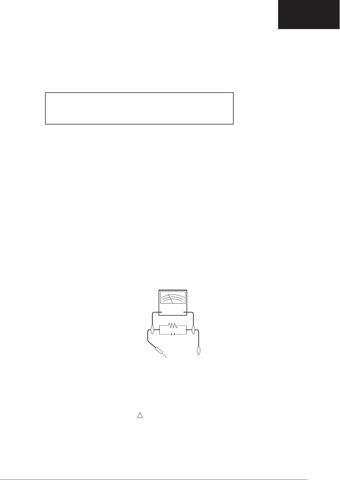
3. To be sure that no shock hazard exists, check for leakage current in the following manner.
• Plug the AC cord directly into a 220~240 volt AC outlet. (Do not use an isolation transformer for this test).
•Using two clip leads, connect a 1.5k ohm, 10 watt resistor paralleled by a 0.15µF capacitor in series with all exposed metal
cabinet parts and a known earth ground, such as electrical conduit or electrical ground connected to an earth ground.
•A true RMS reading multimeter should be used for this test, especially where the equipment uses a switch mode
power supply which may result in very non-sinusoidal leakage current.
•Connect the resistor connection to all exposed metal parts having a return to the chassis (antenna, metal cabinet,
screw heads, knobs and control shafts, escutcheon, etc.) and measure the AC voltage drop across the resistor.
LC-32LE511
LC-40LE511
LC-40LE531
All checks must be repeated with the AC cord plug connection reversed. (If necessary, a nonpolarized adaptor plug must
be used only for the purpose of completing these checks.)
Any reading of 1.05V peak (this corresponds to 0.7 mA. peak AC.) or more is excessive and indicates a potential shock
hazard which must be corrected before returning the monitor to the owner.
DVM
AC SCALE
1.5k ohm
10W
0.15 µF
TEST PROBE
TO EXPOSED
METAL PARTS
CONNECT TO
KNOWN EARTH
GROUND
SAFETY NOTICE
Many electrical and mechanical parts in LCD television have special safety-related characteristics.
These characteristics are often not evident from visual inspection, nor can protection afforded by them be necessarily
increased by using replacement components rated for higher voltage, wattage, etc.
Replacement parts which have these special safety characteristics are identied in this manual; electrical components
having such features are identied by “ “.
!
For continued protection, replacement parts must be identical to those used in the original circuit.
The use of a substitute replacement parts which do not have the same safety characteristics as the factory recommended
replacement parts shown in this service manual, may create shock, re or other hazards.
7
Page 8
LC-32LE511
L F a
LC-40LE511
LC-40LE531
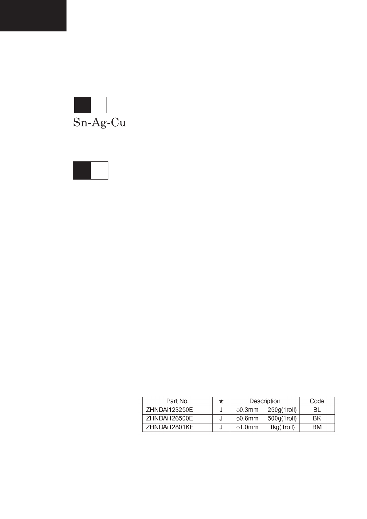
PRECAUTIONS FOR USING LEAD-FREE SOLDER
1 Employing lead-free solder
“ALL PWB” of this model employs lead-free solder. The LF symbol indicates lead-free solder, and is attached on the
PWBs and service manuals. The alphabetical character following LF shows the type of lead-free solder.
Example:
Indicates lead-free solder of tin, silver and copper.
L F n
Sn-Ag-Ni
2 Using lead-free wire solder
When xing the PWB soldered with the lead-free solder, apply lead-free wire solder. Repairing with conventional lead
wire solder may cause damage or accident due to cracks.
As the melting point of lead-free solder (Sn-Ag-Cu) is higher than the lead wire solder by 40°C, we recommend you to
use a dedicated soldering bit, if you are not familiar with how to obtain lead-free wire solder or soldering bit, contact our
service station or service branch in your area.
3 Soldering
As the melting point of lead-free solder (Sn-Ag-Cu) is about 220°C which is higher than the conventional lead solder by
40°C, and as it has poor solder wettability, you may be apt to keep the soldering bit in contact with the PWB for extended
period of time. However, Since the land may be peeled off or the maximum heat-resistance temperature of parts may be
exceeded, remove the bit from the PWB as soon as you conrm the steady soldering condition.
Lead-free solder contains more tin, and the end of the soldering bit may be easily corroded. Make sure to turn on and
off the power of the bit as required.
If a different type of solder stays on the tip of the soldering bit, it is alloyed with lead-free solder. Clean the bit after every
use of it.
When the tip of the soldering bit is blackened during use, le it with steel wool or ne sandpaper.
Be careful when replacing parts with polarity indication on the PWB silk.
Lead-free wire solder for servicing.
Indicates lead-free solder of tin, silver and nickel.
8
Page 9
END OF LIFE DISPOSAL
A. Information on Disposal for Users (private households)
1. In the European Union
Attention: If you want to dispose of this equipment, please do not use the ordinary dust bin!
Used electrical and electronic equipment must be treated separately and in accordance with legislation that requires
proper treatment, recovery and recycling of used electrical and electronic equipment.
Following the implementation by member states, private households within the EU states may return their used
electrical and electronic equipment to designated collection facilities free of charge*. In some countries* your local
retailer may also take back your old product free of charge if you purchase a similar new one.
*) Please contact your local authority for further details.
If your used electrical or electronic equipment has batteries or accumulators, please dispose of these separately
beforehand according to local requirements.
By disposing of this product correctly you will help ensure that the waste undergoes the necessary treatment, recovery
and recycling and thus prevent potential negative effects on the environment and human health which could otherwise
arise due to inappropriate waste handling.
2. In other Countries outside the EU
If you wish to discard this product, please contact your local authorities and ask for the correct method of disposal.
For Switzerland: Used electrical or electronic equipment can be returned free of charge to the dealer, even if you don’t
purchase a new product. Further collection facilities are listed on the homepage of www.swico.ch or www.sens.ch.
B. Information on Disposal for Business Users
1. In the European Union
If the product is used for business purposes and you want to discard it:
Please contact your SHARP dealer who will inform you about the take-back of the product. You might be charged for
the costs arising from take-back and recycling. Small products (and small amounts) might be taken back by your local
collection facilities.
For Spain: Please contact the established collection system or your local authority for take-back of your used
products.
2. In other Countries outside the EU
If you wish to discard of this product, please contact your local authorities and ask for the correct method of disposal.
Attention: Your product
is marked with this
symbol. It means that
used electrical and
electronic products
should not be mixed
with general household
waste. There is a
separate collection
system for these
products.
End of life disposal
The battery supplied with this product contains traces of Lead.
For EU: The crossed-out wheeled bin implies that used batteries should not be put to the general household waste!
There is a separate collection system for used batteries, to allow proper treatment and recycling in accordance with
legislation. Please contact your local authority for details on the collection and recycling schemes.
For Switzerland: The used battery is to be returned to the selling point.
For other non-EU countries: Please contact your local authority for correct method of disposal of the used battery.
LC-32LE511
LC-40LE511
LC-40LE531
LC-32LE511
LC-40LE511
LC-40LE531
9
Page 10
LC-32LE511
LC-40LE511
LC-40LE531
OPERATION MANUAL
Remote Control Buttons
Standby1.
Image size2.
Sleep Timer3.
Mono/Stereo - Dual I-II / Currrent Language 4.
(*) (in DVB channels) / Play preview (in Media
Browser mode)
Favourite Mode Selection (in DVB channels)5.
Numeric buttons6.
Electronic programme guide(in DVB channels)7.
No function8.
Media Browser9.
Navigation buttons (Up/Down/Left/Right)10.
No function11.
No function12.
Programme Down / Page up - Programme Up / 13.
Page down
Mute14.
No function / Record programme15.
Pause (in Media Browser mode) / Timeshift 16.
recording
Rapid reverse (in Media Browser mode)17.
Play (in Media Browser mode)18.
Red button19.
Green button 20.
Picture mode selecion. / Changes picture mode 21.
(in Media Browser video mode)
No function22.
Teletext / Mix (in TXT mode)23.
Subtitle on-off (in DVB channels) / TXT Subtitle 24.
(analogue TV mode) / Subtitle (Media Browser
video mode)
Previous programme25.
AV / Source selection26.
Menu on-off27.
Okay / Select / Hold (in TXT mode) /Channel 28.
List
Exit29.
No function30.
Info / Reveal (in TXT mode)31.
Volume Up / Down32.
No function33.
No function34.
Rapid advance (in Media Browser mode)35.
Stop (in Media Browser mode)36.
Blue button37.
Yellow button: Activates channel list38.
10
Page 11
Operation Manual (Continued)
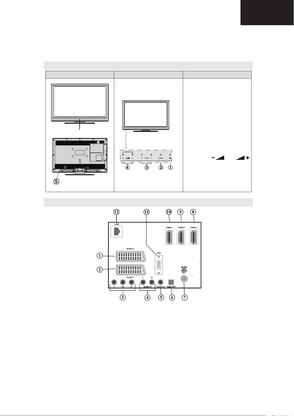
LCD TV and Operating Buttons
FRONT and REAR VIEW Control buttons VIEW Control Buttons
Standby-LED
LC-32LE511
LC-40LE511
LC-40LE531
Standby/On button1.
TV/AV button2.
Programme Up/Down 3.
buttons
Volume Up/Down buttons4.
The Power-switch is used for 5.
turning the TV “Off” or into
“Standby-Mode”
Viewing the Connections- Back Connectors
Note: Press “
buttons at the same time to view
main menu.
” and
LC-32LE511
LC-40LE511
LC-40LE531
EXT 21. inputs or outputs for external devices.
EXT 12. inputs or outputs for external devices. Connect the SCART cable between SCART socket on the
TV and SCART socket on your external device (such as a decoder, a VCR or a DVD player).
Note: If an external device is connected via the SCART socket, the TV will automatically switch to AV
mode.
Note: SCART cable not supplied.
Component Video Inputs (YPbPr)3. are used for connecting component video.
You can connect the component video and audio sockets with a device that has component output.
Connect the component video cables between the COMPONENT VIDEO INPUTS on on the TV and
the component video outputs of your device. While connecting, be sure that the letters on your TV, “Y”,
“Pb”, “Pr” correspond with your device’s connectors.
English - 11 -
11
Page 12
LC-32LE511
LC-40LE511
LC-40LE531
Operation Manual (Continued)
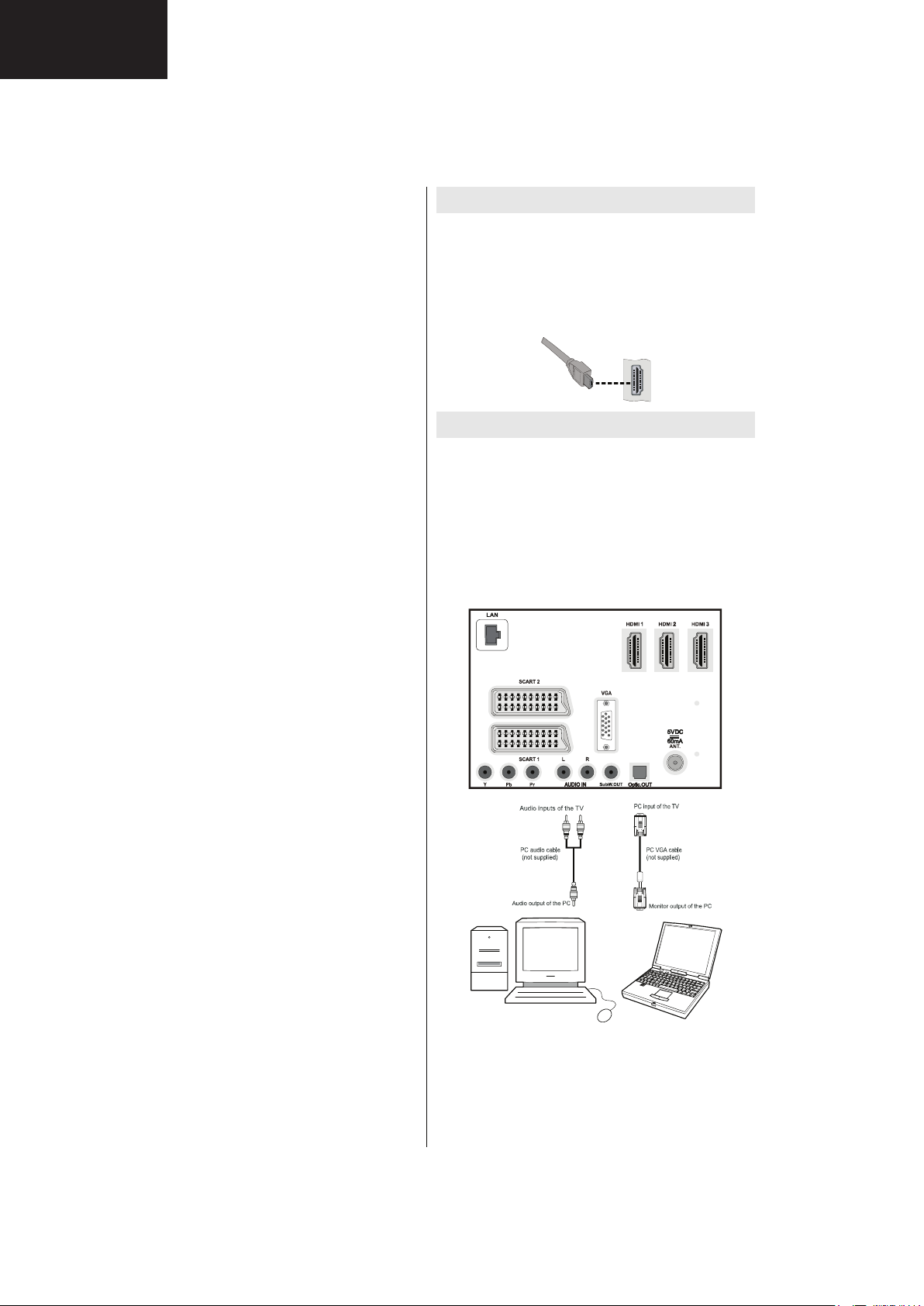
PC/YPbPr Audio Inputs4. are used for connecting audio signals of a PC or a device that connects to the
TV via YPbPr. Connect the PC audio cable between the AUDIO INPUTS on the TV and audio output
of your PC to enable PC audio. Connect the audio cable between AUDIO INPUTS on the TV and audio
outputs of your device to enable component audio.
Subwoofer Out5. is for connecting an external, active subwoofer to the set to give a much deeper bass
effect. Use an appropriate RCA cable to connect the set to a subwoofer unit.
S/PDIF Digital Out6. outputs digital audio signals of the currently watched source.
Use a digital optic cable to transfer audio signals to a device that has S/PDIF input.
RF Input7. connects to an aerial or cable system.
Note that if you use a decoder or a media recorder, you should connect the aerial cable through the
device to the television with an appropriate antenna cable, as shown in the illustration in the following
pages.
HDMI 3: HDMI Input8.
HDMI 2: HDMI Input9.
HDMI 1: HDMI Input10.
HDMI Inputs are for connecting a device that has an HDMI socket. Your LCD TV is capable of
displaying High De nition pictures from devices such as a High De nition Satellite Receiver or DVD
Player. These devices must be connected via the HDMI sockets or Component Socket. These sockets
can accept either 720p or 1080p (optional) signals. No sound connection is needed for an HDMI to
HDMI connection.
PC Input11. is for connecting a personal computer to the TV set.
Connect the PC cable between the PC INPUT on the TV and the PC output on your PC
Ethernet input (for service).12.
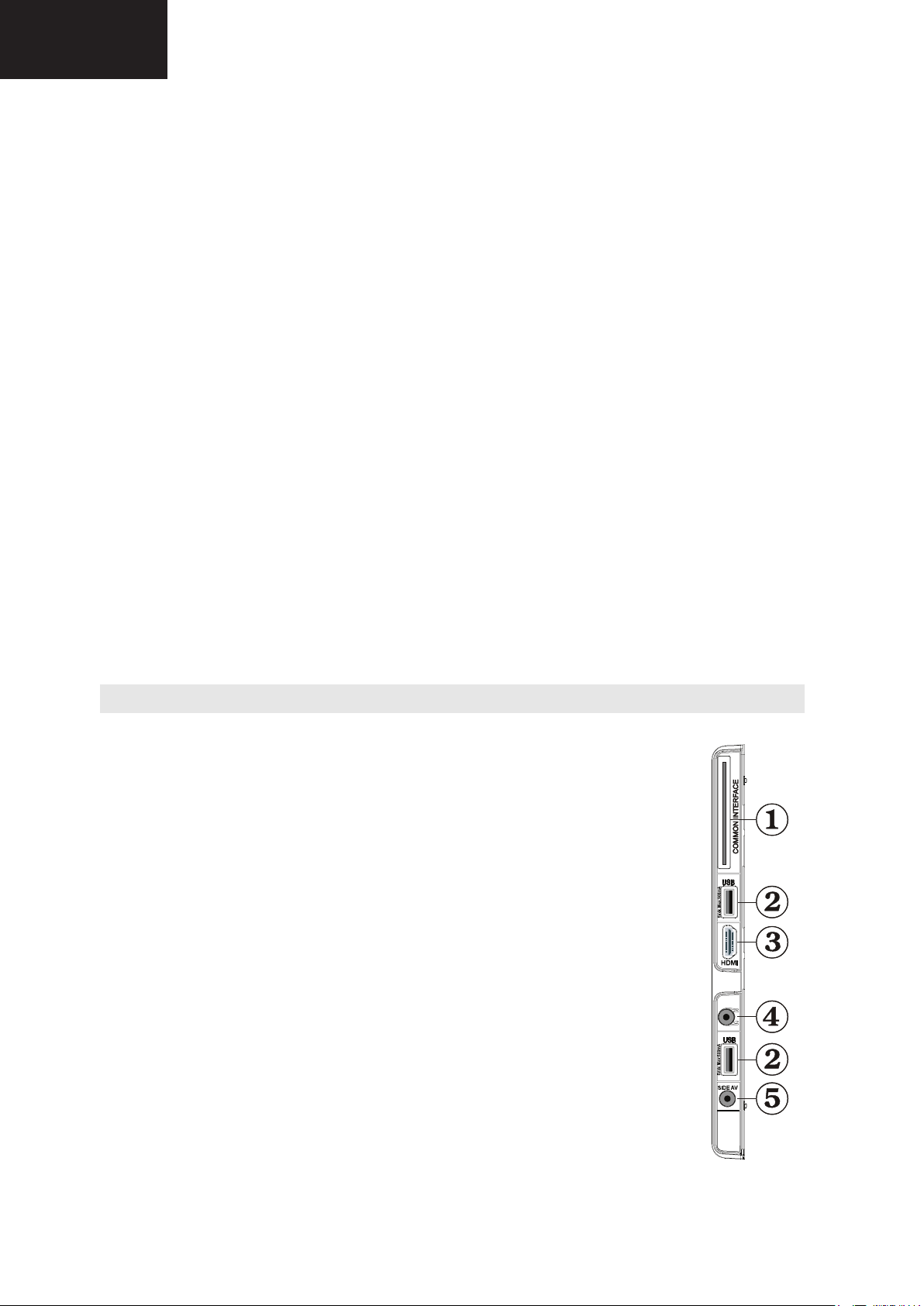
Viewing the Connections - Side Connectors
CI Slot is used for inserting a CI card. A CI card allows you to view all the channels that you subscribe 1.
to. For more information, see “Conditional Access” section.
USB Inputs. 2.
Note that programme recording feature is available via these USB inputs. You can connect external
hard disk drives to this input.
Side HDMI Input (HDMI 4) is for connecting a device that has an HDMI socket.3.
Headphone jack is used for connecting an external headphone to the system. Connect 4.
to the HEADPHONE jack to listen to the TV from headphones (optional).
Side audio-video connection5. input is used for connecting video and audio signals
of external devices. To make a video connection, you must use the supplied AV
connection cable for enabling connection. First, plug singular jack of the cable to the
TV’s Side AV socket. Afterwards, insert your video cable’s (not supplied) connector into
the YELLOW input (located on the plural side) of the supplied AV connection cable.
Colours of the connected jacks should match.
To enable audio connection, you must use RED and WHITE inputs of the side AV
connection cable. Afterwards, insert your device’s audio cable’s connectors into
the RED and WHITE jack of the supplied side AV connection cable. Colours of the
connected jacks should match.
Note: You should use audio inputs of side AV connection cable (RED & WHITE)
to enable sound connection when connecting a device to your TV by using PC or
COMPONENT VIDEO input.
12
Page 13
Operation Manual (Continued)
(Tera Byte) or more le capacity, you can experience
it is recommended that you rst format the disk using
LC-32LE511
LC-40LE511
LC-40LE531
Power Connection
IMPORTANT: The TV set is designed to operate on
220-240V AC, 50 Hz socket.
After unpacking, allow the TV set to reach the •
ambient room temperature before you connect the
set to the mains.
Plug the power cable to the mains socket outlet.•
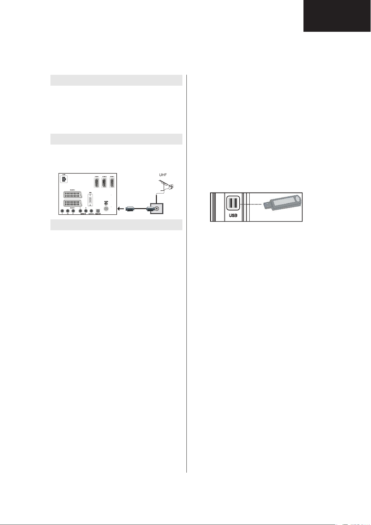
Antenna Connection
Aerial Connection
Connect the aerial TV plug to the AERIAL INPUT •
socket located at the rear of the TV.
Using USB Inputs
USB Connection
You can connect a USB hard disk drive or USB •
memory stick to your TV by using the USB inputs
of the TV. This feature allows you to play les stored
in a USB drive or record programmes.
2.5” and 3.5” inch (hdd with external power supply) •
external hard disk drives are supported.
To record a programme, you should rst connect •
a USB disk to your TV while the TV is switched
off. You should then switch on the TV to enable
recording feature. Otherwise, recording feature will
not be available.
IMPORTANT !
You should back up your les before making any •
connections to the TV set in order to avoid any
possible data loss. Note that manufacturer will not
be responsible for any le damage or dataloss.
It is possible that certain types of USB devices (e.g. •
MP3 Players) or USB hard disk drives/memory sticks
may not be compatible with this TV.
IMPORTANT: The TV supports only FAT32 disk
formatting. NTFS format is not supported. If you
connect a USB disk with NTFS format, the TV will ask
you to format the content. See the section, “Format
Disk” in the following pages for more information on
disk formatting.
Note that ALL the data stored on the USB disk will
be lost and then the disk format will be converted to
FAT32 in such a case.
USB Disk Connection
• Plug your USB device to the USB input of the TV.
Note: Plug or unplug your USB disk while the TV is
switched off.
Note: If you are going to connect a USB hard disk
drive to the TV set, USB connection cable used
between the disk drive and the TV should have a USB
logo and should be as short as possible.
Note: While formatting a USB hard disk that has 1TB
problems with the formatting process. In such a
case, you should format the disk with your personal
computer and the formatted disk type should be
FAT32.
SIDE VIEW USB MEMORY
LC-32LE511
LC-40LE511
LC-40LE531
CAUTION !
Quickly plugging and unplugging USB devices, •
is a very hazardous operation. Especially, do not
repeatedly quickly plug and unplug the drive. This
may cause physical damage to the USB player and
especially the USB device itself.
Do not pull out USB module while playing or •
recording a le.
Programme Recording
To record a programme, you should rst connect a
USB disk to your TV while the TV is switched off.
You should then switch on the TV to enable recording
feature.
IMPORTANT: When using a new USB hard disk drive,
your TV’s “Format Disk” option.
To use the recording function a USB 2.0 certi ed •
device of at least 1GB should be used, If the
connected USB device is not USB 2.0 an error
message will be displayed.
Recorded programmes are saved into the connected •
USB disk in .TS format (MPEG-2 transport stream).
If desirable, you can back up / copy these saved
recordings into a personal computer.
Note: It is possible that recorded broadcasts in
TS format may not be supported by your media
playback software. In such a case, you should install
an appropriate media playback software to your
computer.
An hour of the recordings stored occupies •
approximately 2 GB of space.
13
Page 14
LC-32LE511
LC-40LE511
LC-40LE531
Operation Manual (Continued)
For more information on recording programmes, •
see sections “Instant Recording”, “Timeshifting”,
“Electronic Programme Guide”, “Recordings Library”
or “Recording Timers” in the following parts.
Recorded programmes are stored in the following •
directory of the connected USB disk: \DVR\RECS.
All recordings are indicated with a number (such
as 4801-000.ts). A text (txt) le is created for each
recording. This text le includes information such as
broadcaster, programme, and recording time.
If the writing speed of the connected USB disk is not •
suf cient, recording may fail and timeshifting feaute
may not be available.
Recordings of HD programmes can occupy bigger •
size on the USB disk depending on the broadcast’s
resolution. For this reason it is recommended
to use USB hard disk drives for recording HD
programmes.
Do not plug out the USB/HDD during the recording. •
This may harm the connected USB/HDD.
Only two partitions on a HDD unit can be •
supported.
Some stream packets may not be recorded because •
of signal problems, so sometimes video may freezes
during playback.
Record, Play, Pause, Display (for PlayListDialog) •
keys could not be used when teletext is ON. If a
recording starts from timer when teletext is ON,
teletext is automatically turned off. Also teletext
usage is disabled when there is ongoing recording
or playback.
Note: If the recording time of an event is longer than
the memory capacity, the following message will
appear on the screen: “There is not enough space for
‘event’ but it will be recorded until the drive is full”.
Side HDMI Connection (HDMI 4)
The side HDMI is convenient connection for external
HDMI devices, use an appropriate HDMI cable and
ensure both the TV and external device are switched
off before making the connection. Select HDMI 4 from
the Source list to access this input.
HDMI DEVICE SIDE VIEW
Connecting the LCD TV to a PC
For displaying your computer’s screen image on your
LCD TV, you can connect your computer to the TV set.
Power off both computer and display before making
any connections. Use 15-pin D-sub display cable to
connect a PC to the LCD TV. When the connection
is made, switch to PC source. See “Input selection”
section. Set the resolution that suits your viewing
requirements. Resolution information can be found
in the appendix parts.
14
Page 15
Operation Manual (Continued)
LC-32LE511
LC-40LE511
LC-40LE531
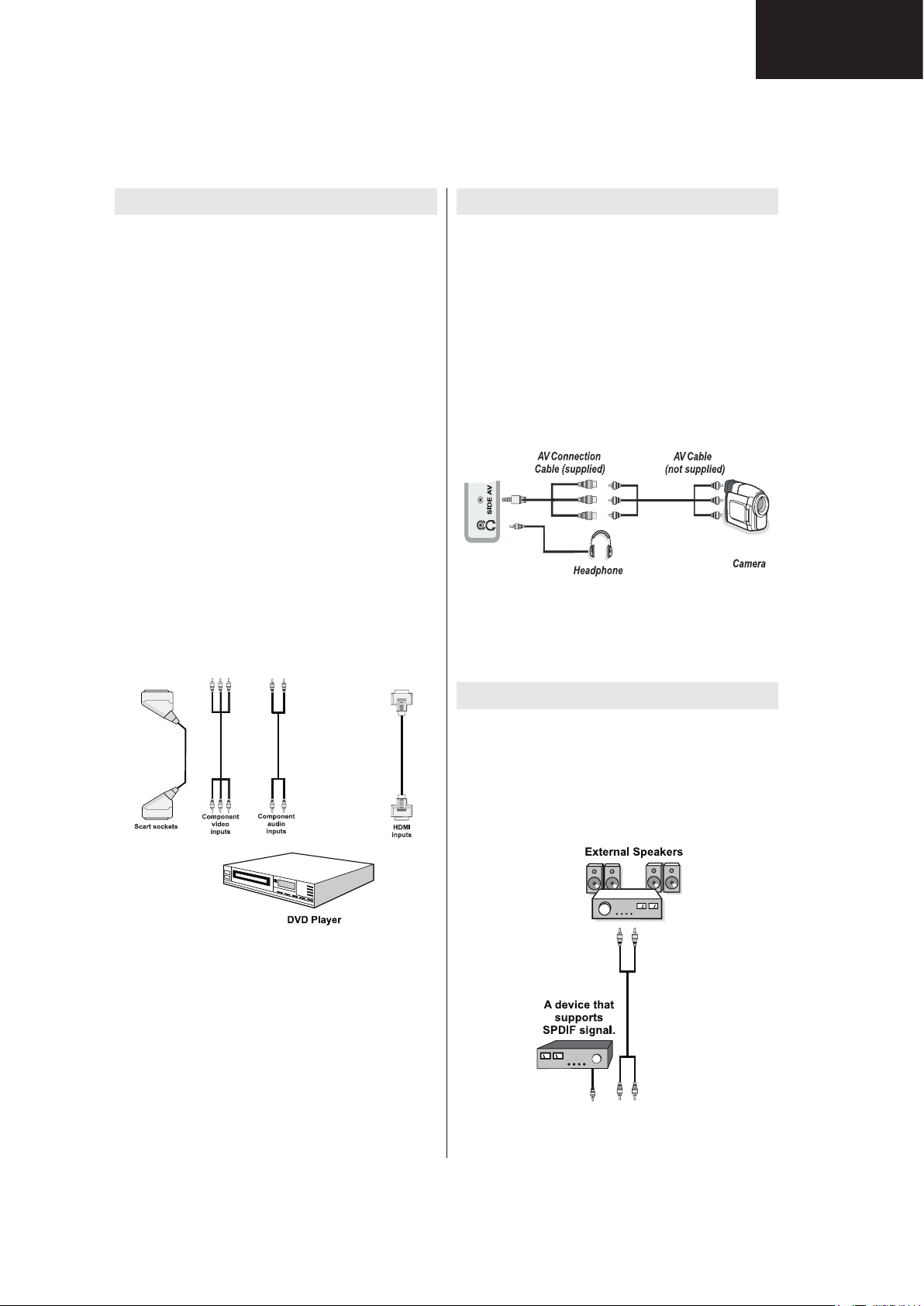
Connecting to a DVD Player
If you want to connect a DVD player to your LCD
TV, you can use connectors of the TV set. DVD
players may have different connectors. Please refer
to your DVD player’s instruction book for additional
information. Power off both the TV and the device
before making any connections.
Note: Cables shown in the illustration are not
supplied.
If your DVD player has an HDMI socket, you can •
connect via HDMI. When you connect to DVD player
as illustrated below, switch to HDMI source. See,
“Input Selection” section.
Most DVD players are connected through •
COMPONENT SOCKETS. Use a component video
cable to connect video input. For enabling audio, use
a component audio cable as illustrated below. When
the connection is made, switch to YPbPr source.
See, “Input selection” section.
You may also connect through the SCART 1 or •
SCART 2. Use a SCART cable as shown below.
Note: These three methods of connection perform the
same function but in different levels of quality. It is not
necessary to connect by all three methods.
Using Side AV Connectors
You can connect a range of optional equipment to your
LED TV using side connectors of the TV.
For connecting a camcorder or camera , you should •
use AV socket (side). To do this, you must use the
supplied video/audio connection cable. First, plug
single jack of the cable to the TV’s AV IN socket
(side). Afterwards, insert your camera cable’s (not
supplied) connectors into the plural part of the video/
audio connection cable. Colours of the connected
jacks should match. See illustration below.
Afterwards, you should switch to • S id e AV source. See
the section Input selection in the following sections
for more information.
LC-32LE511
LC-40LE511
LC-40LE531
To listen the TV sound from headphones, you •
should connect headphones to your TV by using the
HEADPHONE jack as illustrated above.
Using Other Connectors
You can connect a range of optional equipment
to your LCD TV. Possible connections are shown
below. Note that cables shown in the illustration are
not supplied.
For connecting a to a device that has SPDIF support, •
use an appropriate SPDIF cable to enable sound
connection.
15
Page 16
LC-32LE511
LC-40LE511
LC-40LE531
Operation Manual (Continued)
Remote Control Handset
Remove the battery cover located on the back of •
the remote control by gently pulling backwards from
the indicated part.
Insert two • AAA/R3 or equivalent type batteries
inside. Observe the correct polarity (+/-) when
inserting batteries and replace the battery cover.
Note: Remove the battery from remote control when
it is not to be used for a long period. Otherwise it can
be damaged due to any leakage of batteries.
Switching the TV On/Off
To Switch the TV On
Connect the power cord to the 220-240V AC 50 Hz.
Switch the “•
to position “|” so the TV will switch to standby mode.
Then the standby LED lights up.
To switch on the TV from standby mode either:•
Press the “• ” button, P+ / P- or a numeric button
on the remote control.
Press the “•
The TV will then switch on.•
Note : If you switch on your TV via PROGRAMME
UP/DOWN buttons on the remote control or on the
TV set, the programme that you were watching last
will be reselected.
By either method the TV will switch on.
To Switch the TV to Standby
To switch the TV to low power standby press the
“
” button on the remote control or right hand side
of the TV.
Note: When the TV is switched to standby mode,
standby LED can blink to indicate that features such
as Standby Search, Over Air Download or Timer is
active.
” button on the rear left hand side
” or +/- button on the TV.
To Switch the TV Off
Switch the “• ” button bottom right edge under the
screen to position 2 as illustrated,
TV from the mains, the LED will go out.
If the TV will not be used for a long period i.e. •
holidays, then unplug the power cord from the
mains socket.
to isolate the
Digital Teletext (** for UK only)
Press the “• ” button.
The digital teletext information appears.•
Operate it with the coloured buttons, cursor buttons •
and OK button.
The operation method may differ depending on the
contents of the digital teletext.
Follow the instructions displayed on digital teletext
screen.
When Press “• SELECT” button or similar message
appears on the screen, press the OK button.
When the “•
television broadcasting.
With digital terrestrial broadcasting (DVB-T), in •
addition to digital teletext broadcasting together with
the normal broadcasting, there are also channels
with just digital teletext broadcasting.
The aspect ratio (picture shape) when watching •
a channel with just digital teletext broadcasting is
the same as the aspect ratio of the picture viewed
previously.
When you press the “•
teletext screen will be displayed.
” button is pressed, the TV returns to
” button again, the digital
16
Page 17
LC-32LE511
Speci cations
TV BROADCASTING
PAL/SECAM B/G D/K K’ I/I’ L/L’
RECEIVING CHANNELS
VHF (BAND I/III)
UHF (BAND U)
HYPERBAND
NUMBER OF PRESET CHANNELS
10.000
CHANNEL INDICATOR
On Screen Display
RF AERIAL INPUT
75 Ohm (unbalanced)
OPERATING VOLTAGE
220-240V AC, 50 Hz.
AUDIO OUTPUT POWER (W
RMS.
) (10% THD)
2 x 6
POWER CONSUMPTION (W)
135 W (max)
< 1 W (Standby)
PANEL
Digital Reception (DVB-T)
Transmission Standards:
DVB-T, MPEG2,DVB-T, MPEG4 HD
i. DEMODULATION
-Symbol rate: COFDM with 2K/8K FFT mode.•
-Modulation: 16-QAM - 64-QAM FEC for all DVB •
modes (automatically found)
MHEG-5 ENGINE compliant with ISO/IEC 13522-5 •
UK engine Pro le (UK only)
Object carousel support compliant with ISO/IEC •
135818-6 and UK DTT pro le(UK only)
Frequency range: 474-850 MHz for UK models•
ii. VIDEO
-H.264 (MPEG-4 part 10) main and high pro le level •
4.1/MPEG-2 MP@HL video decoder.
-HD display multi format capable (1080i, 720p, •
576p)
-CVBS analogue output.(In HD channels, this will •
not be available
iii. AUDIO
-MPEG-1 layer I/II, MPEG-2 layer II, AAC, HEAAC, •
AC3, E-AC3
-Sampling frequencies supported are 32, 44.1 & •
48 kHz
Digital Reception (DVB-T2)
Demodulation
-QPSK, 16QAM, 64QAM, 256QAM with 1k, 2k, 4k,
8k, 16k, 32k FFT mode
Frequency Band
- UHF/ VHF
Channel BW
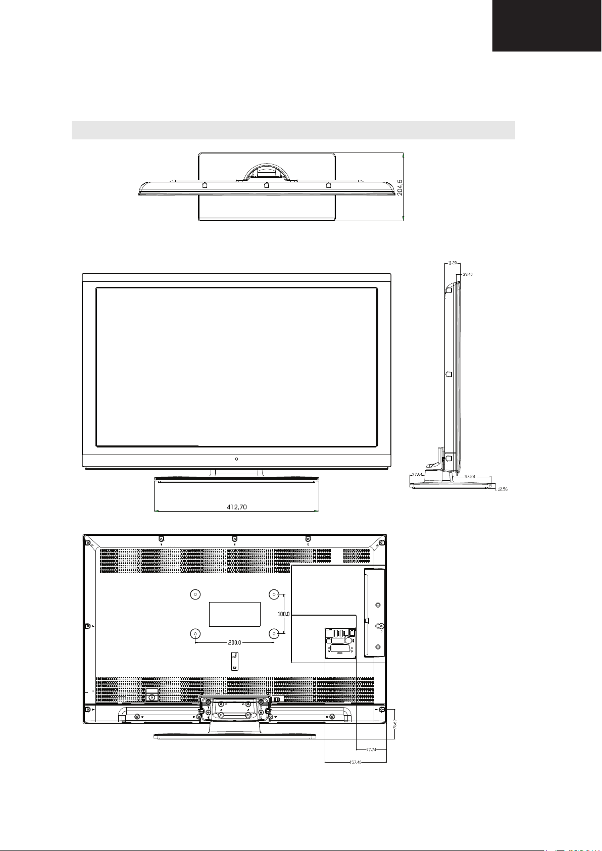
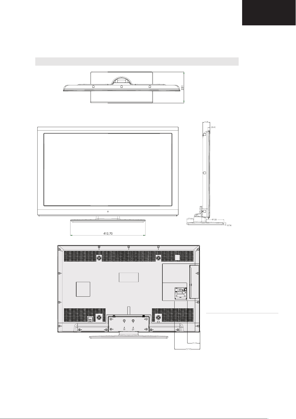
Dimensional Drawings
LC-32LE511
LC-40LE511
LC-40LE531
DIMENSIONS
17
LC-32LE511
LC-40LE511
LC-40LE531
32” (80 cm) wide screen
VESA
200 x 100 mm / M4
DIMENSIONS (mm)
DxLxH (With foot): 205,5 x 773 x 522
Weight (Kg): 10,50
DxLxH (Without foot): 39 x 773 x 490
Weight (Kg): 9,20
Page 18
LC-32LE511
Specifi cations
TV BROADCASTING
PAL/SECAM B/G D/K K’ I/I’ L/L’
RECEIVING CHANNELS
VHF (BAND I/III)
UHF (BAND U)
HYPERBAND
NUMBER OF PRESET CHANNELS
10.000
CHANNEL INDICATOR
On Screen Display
RF AERIAL INPUT
75 Ohm (unbalanced)
OPERATING VOLTAGE
220-240V AC, 50 Hz.
AUDIO OUTPUT POWER (W
RMS.
) (10% THD)
2 x 8
POWER CONSUMPTION (W)
150 W (max)
< 1 W (Standby)
-CVBS analogue output.(In HD channels, this will•
not be available
iii. AUDIO
-MPEG-1 layer I/II, MPEG-2 layer II, AAC, HEAAC,•
AC3, E-AC3
-Sampling frequencies supported are 32, 44.1 &•
48 kHz
Digital Reception (DVB-C)
Transmission Standards:
DVB-C, MPEG2, DVB-C, MPEG4
i. DEMODULATION
-Symbolrate: 4.0 Msymbols/s to 7.2 Msymbols/s
- Modulation: 16-QAM , 32-QAM ,64-QAM, 128-QAM
and 256-QAM
ii. VIDEO
- All MPEG2 MP@ML formats with up-conversion and
ltering to CCIR601 format.
-CVBS analogue output
iii. AUDIO
-All MPEG1 Layer 1 and 2 modes
-Sampling frequencies supported are 32, 44.1 & 48
kHz.
Digital Reception (DVB-T2)
Demodulation
-QPSK, 16QAM, 64QAM, 256QAM with 1k, 2k, 4k,
8k, 16k, 32k FFT mode
Frequency Band
- UHF/ VHF
LC-40LE511
LC-40LE531
LC-40LE511E
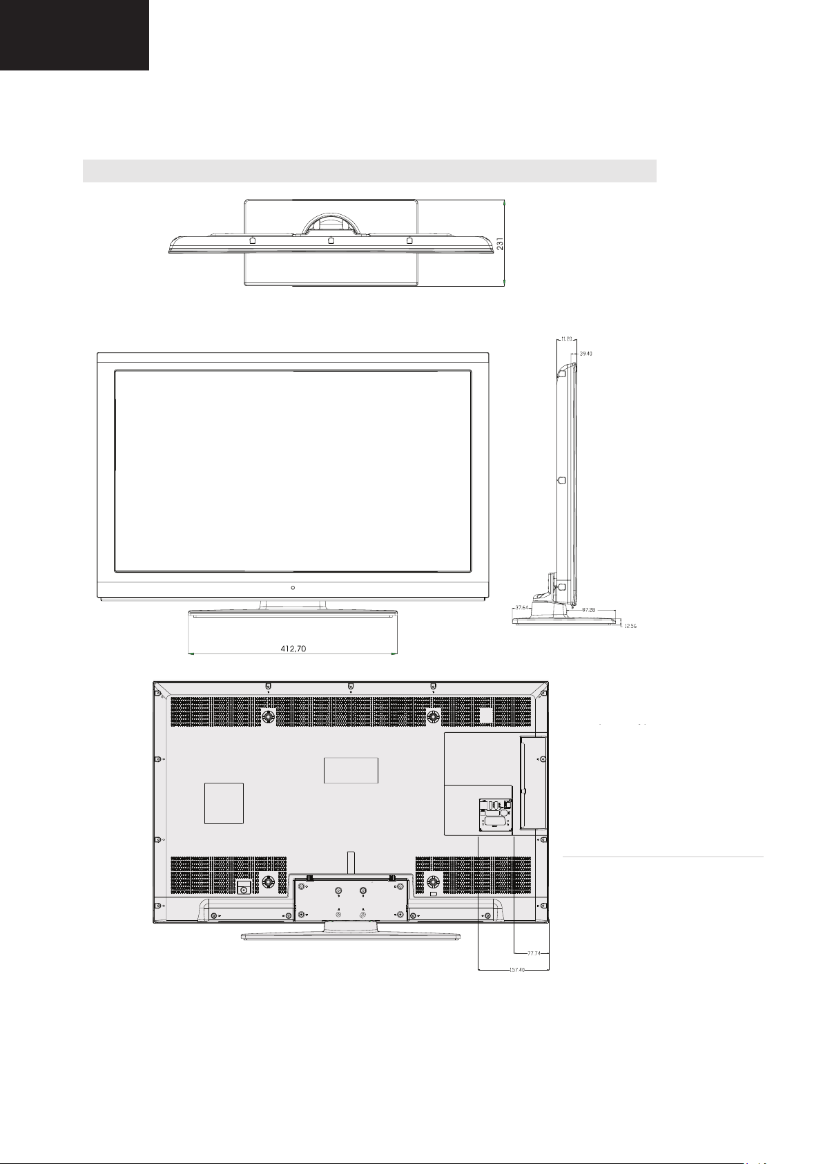
Dimensional Drawings
DIMENSIONS
18
PAN E L
40” (102 cm) wide screen
DIMENSIONS (mm)
DxLxH (With foot): 232 x 959 x 627
Weight (Kg): 15,20
DxLxH (Without foot): 40 x 959 x 593
Weight (Kg): 12,50
Page 19
LC-40LE531E
Specications
TV BROADCASTING
PAL/SECAM B/G D/K K’ I/I’ L/L’
RECEIVING CHANNELS
VHF (BAND I/III)
UHF (BAND U)
HYPERBAND
NUMBER OF PRESET CHANNELS
10.000
CHANNEL INDICATOR
On Screen Display
RF AERIAL INPUT
75 Ohm (unbalanced)
OPERATING VOLTAGE
220-240V AC, 50 Hz.
AUDIO OUTPUT POWER (W
RMS.
) (10% THD)
2 x 8
POWER CONSUMPTION (W)
150 W (max)
< 1 W (Standby)
-CVBS analogue output.(In HD channels, this will•
not be available
iii. AUDIO
-MPEG-1 layer I/II, MPEG-2 layer II, AAC, HEAAC,•
AC3, E-AC3
-Sampling frequencies supported are 32, 44.1 &•
48 kHz
Digital Reception (DVB-C)
Transmission Standards:
DVB-C, MPEG2, DVB-C, MPEG4
i. DEMODULATION
-Symbolrate: 4.0 Msymbols/s to 7.2 Msymbols/s
- Modulation: 16-QAM , 32-QAM ,64-QAM, 128-QAM
and 256-QAM
ii. VIDEO
- All MPEG2 MP@ML formats with up-conversion and
ltering to CCIR601 format.
-CVBS analogue output
iii. AUDIO
-All MPEG1 Layer 1 and 2 modes
-Sampling frequencies supported are 32, 44.1 & 48
kHz.
Digital Reception (DVB-T2)
Demodulation
-QPSK, 16QAM, 64QAM, 256QAM with 1k, 2k, 4k,
8k, 16k, 32k FFT mode
Frequency Band
- UHF/ VHF
Dimensional Drawings
LC-32LE511
LC-40LE511
LC-40LE531
DIMENSIONS
19
LC-32LE511
LC-40LE511
LC-40LE531
PAN E L
40” (102 cm) wide screen
DIMENSIONS (mm)
DxLxH (With foot): 232 x 959 x 627
Weight (Kg): 15,20
DxLxH (Without foot): 40 x 959 x 593
Weight (Kg): 12,50
Page 20

LC-32LE511
LC-40LE511
LC-40LE531
17MB70-2 mainboard is based on Broadcom concept IC. This IC combines DVB-T COFDM
terrestrial and PAL/SECAM demodulators, HDMI receivers, a transport processor, a digital
audio processor, graphics processing, Ethernet MAC and PHY, digital processing of analog
video and audio, analog video digitizer and DAC functions, stereo high-fidelity audio DACs,
a 400-MHz dual-threaded MIP processor, and a peripheral control unit providing a variety of
television control functions. This IC also features an advanced video decoder capable of
supporting high-definition AVC, VC-1, and DVB-T MPEG-2 streams.
• Advanced multiformat decoder supporting the following:
• 3D/2D OpenGL® ES 1.0- compliant graphics core
• Integrated Video Processing:
• Dual HDMI 1.3a receivers
• Extensive audio support:
• Ethernet MAC and PHY
• Integrated DVB-T COFDM terrestrial demodulator:
• Integrated PAL/SECAM Demodulator
• PAL decoder with a 3D/2D comb
• Direct PC input support up to 1600 x 1200 UXGA
• Integrated dual-link LVDS transmitters
• Dual USB 2.0
• A 400-MHz 32-bit MIPS dual CPU with two 32-KB instruction caches
and a combined 64-KB data cache with 128-KB L2 cache
INTRODUCTION
1. INTRODUCTION
Main IC Features:
- H.264/AVC Main and High Profile to Level 4.1 (HD), Level 3.1 (SD)
- HD/SD AVS Jizhun Profile Levels 2.0, 4.0, and 6.0
- VC-1 Advanced Profile @ Level 3, simple and main profiles
- HD/SD MPEG-2 Main Profile at Main and High levels
- MPEG still image decode
- HD DivX® 3.11/4.11/5.x/6x/Home Theater
- 3D Color management
- Digital, Analog, and Mosquito Noise Reduction
- 1080i motion adaptive deinterlacing with 3:2/2:2 pull-down
- True 10-bit video carried through system
- AAC+ Level 2, AAC-HE
- Dolby® Digital, Dolby Digital Plus, Trusurround XT®
- MPEG I layers 1, 2, and 3 (MP3)
- Windows Media® and Windows Media Pro audio
- Audio DACs, input switch, and equalizer
- Standards compliance: ETSI EN 300 744, Nordig Unified v1.0.3, DTG D-Book 5
compliant
- Excellent Doppler performance
- Active impulse noise suppression
20
Page 21

CIRCUIT DESCRIPTIONS
Sound system output is supplying 2x8W (10%THD) for stereo 8speakers
Supported peripherals are:
1 RF input VHF I, VHF III, UHF @ 75Ohm(Common)
1 Side AV (CVBS, R/L_Audio)
2 SCART socket(Common)
1 YPbPr (Common)
1 Side S-Video(Common)
1 PC input(Common)
4 HDMI 1.3 input(Common)
1 Common interface(Common)
1 Optic S/PDIF output(Common)
1 Stereo audio input for PC(Common)
1 Subwoofer output(Common)
1 Headphone(Common)
2 USB(Common)
1 Bluray/DVD(Optional)
1 Ethernet-RJ45 (Common)
1 External Touchpad(Common)
LC-32LE511
LC-40LE511
LC-40LE531
LC-32LE511
LC-40LE511
LC-40LE531
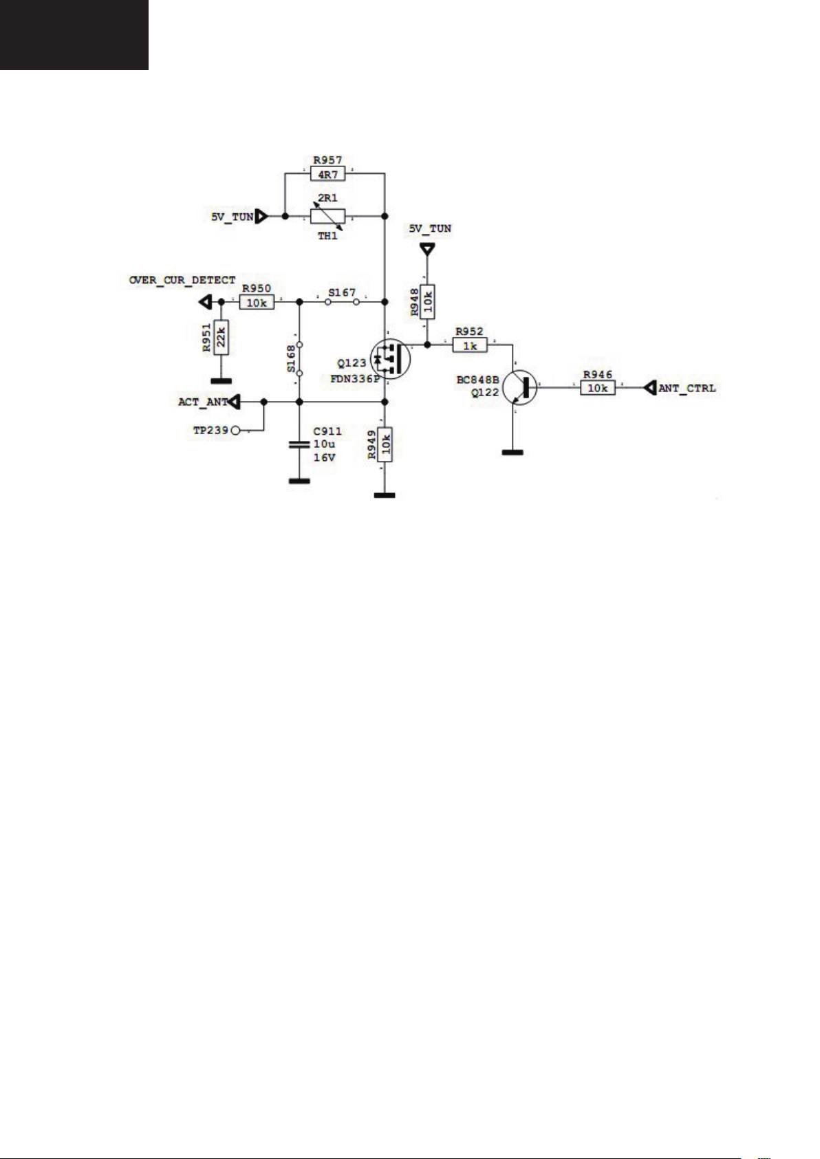
2. TUNER
FT 2112/3/8/9 are newly developed Half-NIM modules designed for both digital
(DVB-T / T2 and DTMB for terrestrial China) and analog TV reception in compliance with
the European ATV standards for analogue, as well as with the terrestrial standard ETS 300
744 for DVB-T and the new terrestrial standard ETS 302 755 for DVB-T2. It consists of a 3band RF tuner, which receives RF signal and down-converts it to an IF frequency of 36MHz
for digital and 38.9MHz for analog IF. The analogue IF output can directly drive a SAW
filter. A digital IF Stage, which consists of one SAW filter & gain-controllable IF that offers a
sufficient output level to be connected directly to an A/D converter.
In active antenna option, the following circuit are used. ANT_CTRL pin is controlled by
microcontroller. If ANT_CTRL is low, ANT_PWR will be low. If ANT_CTRL is high,
ANT_PWR will be high. OVER_CUR_DETECT pin is a monitor for short circuit in antenna.
OVER_CUR_DETECT is low, ANT_CTRL will be low, so ANT_PWR will be low. Finally,
short circuit protection is done by circuits and microcontroller.
21
Page 22
LC-32LE511
LC-40LE511
LC-40LE531
Active Antenna Circuit
1.1. Features of FT2112
• Digital DVB-T T2, DTMB & analogue (48.25MHz to 863.25MHz) reception
• Single 5V supply voltage only
• Built-in 5-33V DC-DC converter
• Single power supply to the RF tuner & IF VGA amplifier section
• Bus Control switch-able RF AGC function:
a) Wide Band AGC for optimum strong signal performance
b) Conventional AGC for optimum analog reception
• RF AGC information via I2C Bus
• Tuner power standby mode via I2C Bus
• Small size (56 mm x 29 mm x 10 mm)
• I2C (SDA & SCL) bus control interface
• ROHS compliant
22
Page 23
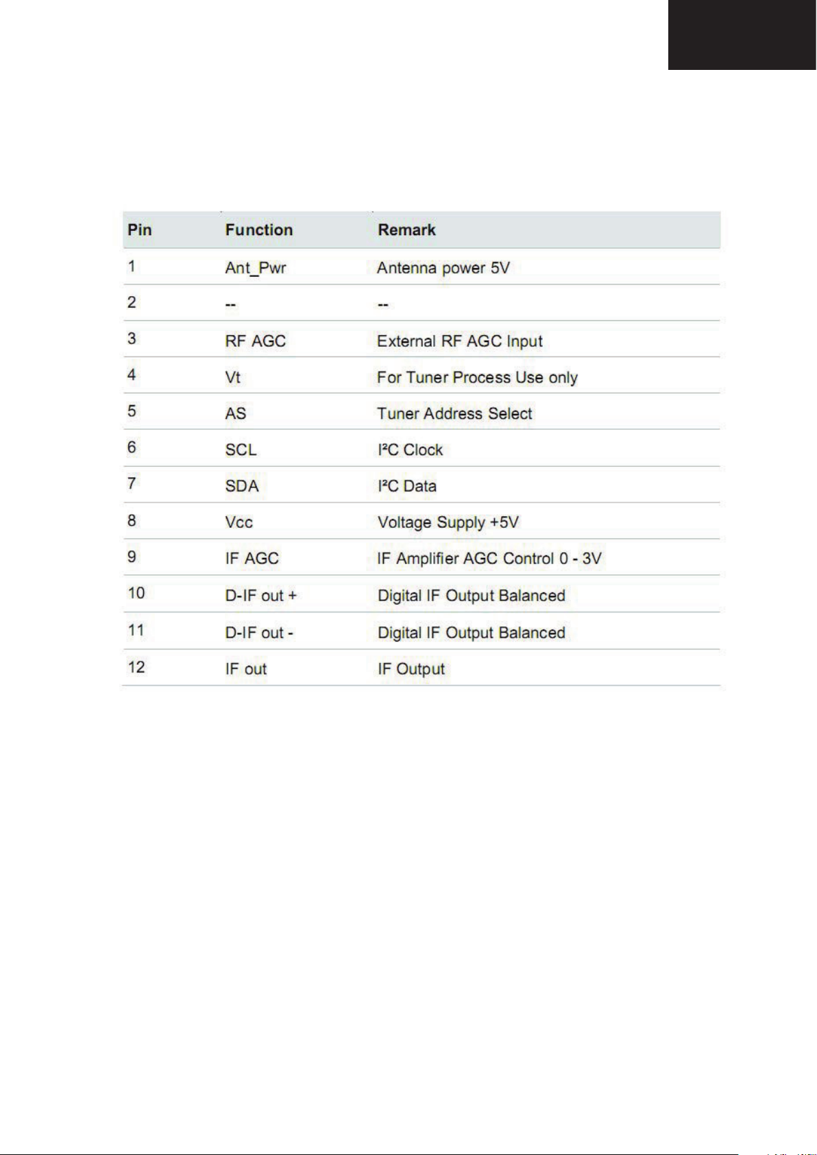
1.2.Tuner Pinning
LC-32LE511
LC-40LE511
LC-40LE531
3. AUDIO AMPLIFIER STAGES
A. MAIN AMPLIFIER (TPA3110)
LC-32LE511
LC-40LE511
LC-40LE531
a. General Description
17MB70 uses TPA 3110 15-W filter-free stereo Class-D audio power amplifier for main
audio output. The TPA3110D2 is a 15-W (per channel) efficient, Class-D audio power
amplifier for driving bridged-tied stereo speakers. Advanced EMI Suppression Technology
enables the use of inexpensive ferrite bead filters at the outputs while meeting EMC
requirements. SpeakerGuard™ speaker protection circuitry includes an adjustable power
limiter and a DC detection circuit. The adjustable power limiter allows the user to set a
"virtual" voltage rail lower than the chip supply to limit the amount of current through the
speaker. The DC detect circuit measures the frequency and amplitude of the PWM signal and
shuts off the output stage if the input capacitors are damaged or shorts exist on the inputs.
23
Page 24
LC-32LE511
LC-40LE511
LC-40LE531
The TPA3110D2 can drive stereo speakers as low as 4 y of the
TPA3110D2, 90%, eliminates the need for an external heat sink when playing music. The
outputs are also fully protected against shorts to GND, VCC, and output-to-output. The shortcircuit protection and thermal protection includes an auto-recovery feature.
• 15-W/ch into an 8--V Supply
• 10-W/ch into 8- 13-V Supply
• 30-W into a 4--V Supply
• 90% Efficient Class-D Operation Eliminates Need for Heat Sinks
• Wide Supply Voltage Range Allows Operation from 8 V to 26 V
b. Features
• Filter-Free Operation
• SpeakerGuard™ Speaker Protection Includes Adjustable Power Limiter plus DC Protection
• Flow Through Pin Out Facilitates Easy Board Layout
• Robust Pin-to-Pin Short Circuit Protection and Thermal Protection with Auto Recovery
Option
• Excellent THD+N / Pop-Free Performance
• Four Selectable, Fixed Gain Settings
• Differential Inputs
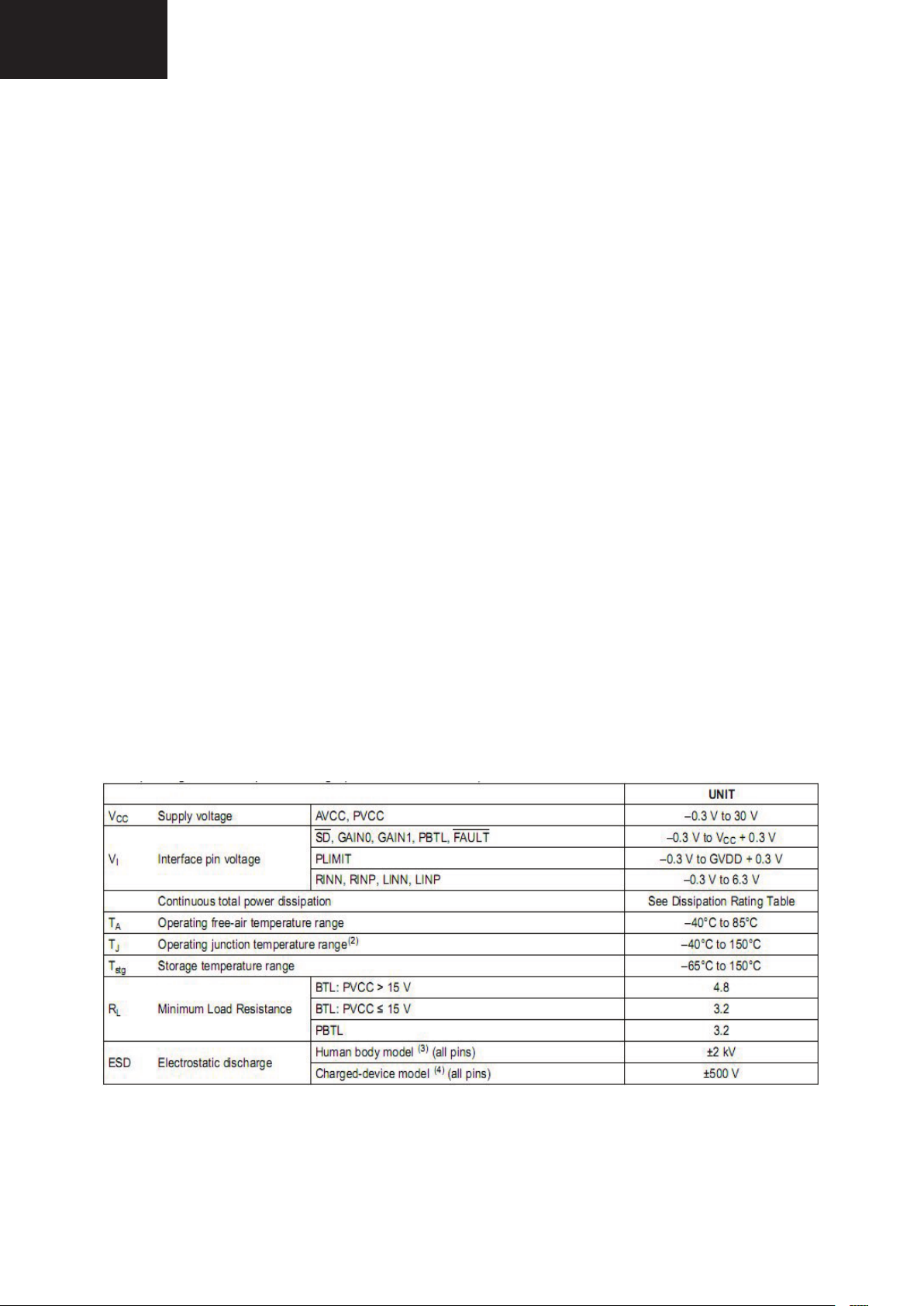
c. Absolute Ratings
24
Page 25
LC-32LE511
LC-40LE511
LC-40LE531
d. Recommended Operating Conditions
e. Pin Functions
.
PIN
I/O/P
NAME
Pin
Number
SD 1 I
FAULT 2 O
LINP 3 I Positive audio input for left channel. Biased at 3V.
LINN 4 I Negative audio input for left channel. Biased at 3V.
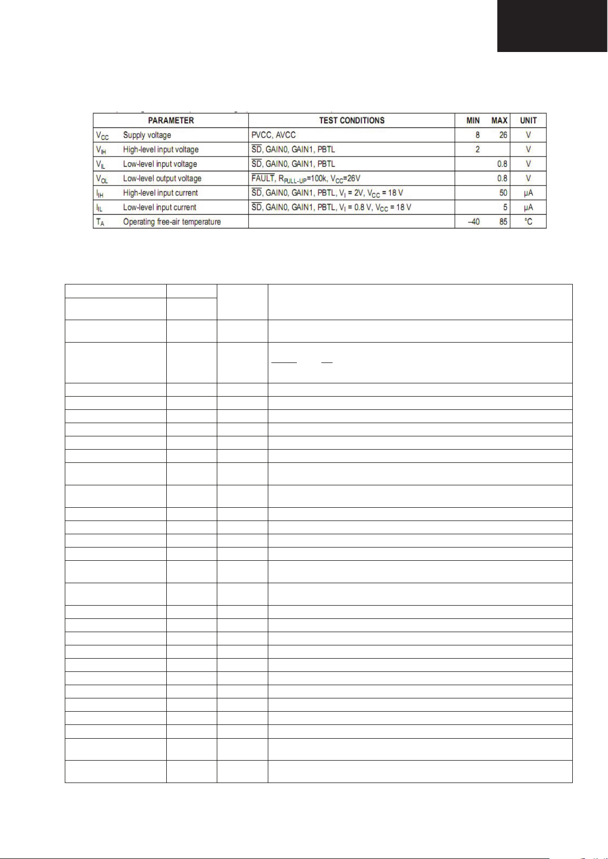
GAIN0 5 I Gain select least significant bit. TTL logic levels with compliance to AVCC.
GAIN1 6 I Gain select most significant bit. TTL logic levels with compliance to AVCC.
AVCC 7 P Analog supply
AGND 8 Analog signal ground. Connect to the thermal pad.
GVDD 9 O
PLIMIT 10 I
RINN 11 I Negative audio input for right channel. Biased at 3V.
RINP 12 I Positive audio input for right channel. Biased at 3V.
NC 13 Not connected
PBTL 14 I Parallel BTL mode switch
PVCCR 15 P
PVCCR 16 P
BSPR 17 I Bootstrap I/O for right channel, positive high-side FET.
OUTPR 18 O Class-D H-bridge positive output for right channel.
PGND 19 Power ground for the H-bridges.
OUTNR 20 O Class-D H-bridge negative output for right channel.
BSNR 21 I Bootstrap I/O for right channel, negative high-side FET.
BSNL 22 I Bootstrap I/O for left channel, negative high-side FET.
OUTNL 23 O Class-D H-bridge negative output for left channel.
PGND
24 Power ground for the H-bridges.
OUTPL 25 O Class-D H-bridge positive output for left channel.
BSPL 26 I Bootstrap I/O for left channel, positive high-side FET.
PVCCL 27 P
PVCCL
28 P
DESCRIPTION
Shutdown
enabled).
Open
compliant
logic input for audio amp (LOW = outputs Hi-Z, HIGH = outputs
TTL logic levels with compliance to AVCC.
drain output used to display short circuit or dc detect fault status. Voltage
to AVCC. Short circuit faults can be set to auto-recovery by connecting
FAULT pin to SD pin. Otherwise, both short circuit faults and dc detect faults must
be reset by cycling PVCC.
High-side FET gate drive supply. Nominal voltage is 7V. Also should be used as
supply for PLIMIT function
Power limit level adjust. Connect a resistor divider from GVDD to GND to set
power limit. Connect directly to GVDD for no power limit.
Power supply for right channel H-bridge. Right channel and left channel power
supply inputs are connect internally.
Power supply for right channel H-bridge. Right channel and left channel power
supply inputs are connect internally.
Power supply for left channel H-bridge. Right channel and left channel power
supply inputs are connect internally.
Power supply for left channel H-bridge. Right channel and left channel power
supply
inputs are connect internally.
LC-32LE511
LC-40LE511
LC-40LE531
25
Page 26
LC-32LE511
LC-40LE511
LC-40LE531
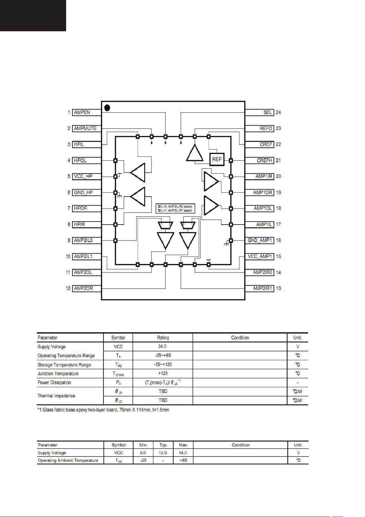
B. LINE-OUT and HEAD-PHONE AMPLIFIER STAGE (CXA3813N)
a. Functional Block Diagram
b. Absolute Ratings
c. Recommended Operating Conditions
26
Page 27
d. Pin Functions
LC-32LE511
LC-40LE511
LC-40LE531
C. SUBWOOFER AMPLIFIER STAGE (TPA3112)
a. General Description
The TPA3112D1 is a 25-W efficient, Class-D audio power amplifier for driving a bridge tied
speaker. Advanced EMI Suppression Technology enables the use of inexpensive ferrite bead
filters at the outputs while meeting EMC requirements. SpeakerGuard speaker protection
system includes an adjustable power limiter and a DC detection circuit. The adjustable power
limiter allows the user to set a "virtual" voltage rail lower than the chip supply to limit the
amount of current through the speaker. The DC detect circuit measures the frequency and
amplitude of the PWM signal and shuts off the output stage if the input capacitors are
damaged or shorts exist on the inputs. The TPA3112D1 can drive a mono speaker as low as
4 eliminates the need for an external heat
sink when playing music. The outputs are fully protected against shorts to GND, VCC, and
output-to-output. The short-circuit protection and thermal protection includes an autorecovery feature.
b. Features
LC-32LE511
LC-40LE511
LC-40LE531
• 25-W into an 8-
• 20-W into an 4-at 10% THD+N From a12-V Supply
• 94% Efficient Class-D Operation into 8-
• Wide Supply Voltage Range Allows Operationfrom 8 to 26 V
• Filter-Free Operation
• SpeakerGuard™ Speaker Protection IncludesAdjustable Power Limiter plus DC Protection
• Flow Through Pin Out Facilitates Easy BoardLayout
• Robust Pin-to-Pin Short Circuit Protection andThermal Protection with Auto-Recovery
Option
• Excellent THD+N/ Pop Free Performance
• Four Selectable, Fixed Gain Settings
• Differential Inputs
27
Page 28
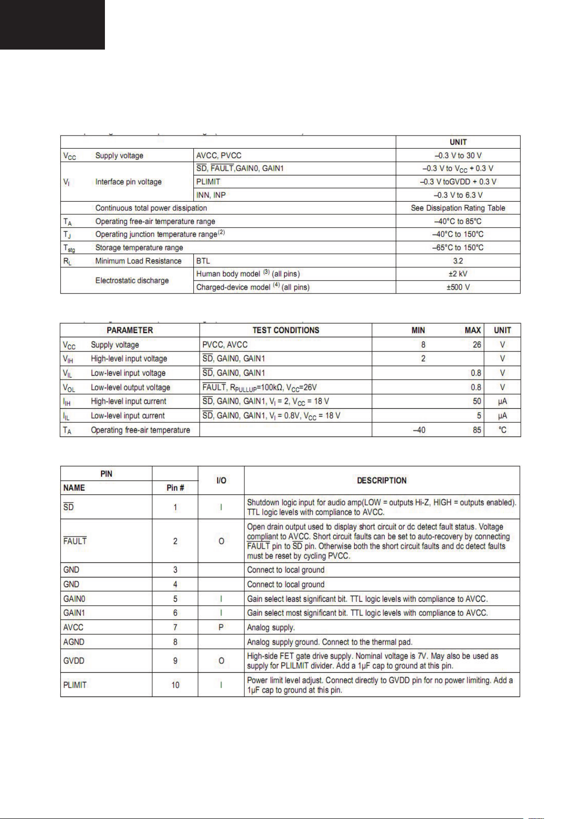
LC-32LE511
LC-40LE511
LC-40LE531
c. Absolute Ratings
d. Recommended Operating Conditions
e. Pin Functions
28
Page 29
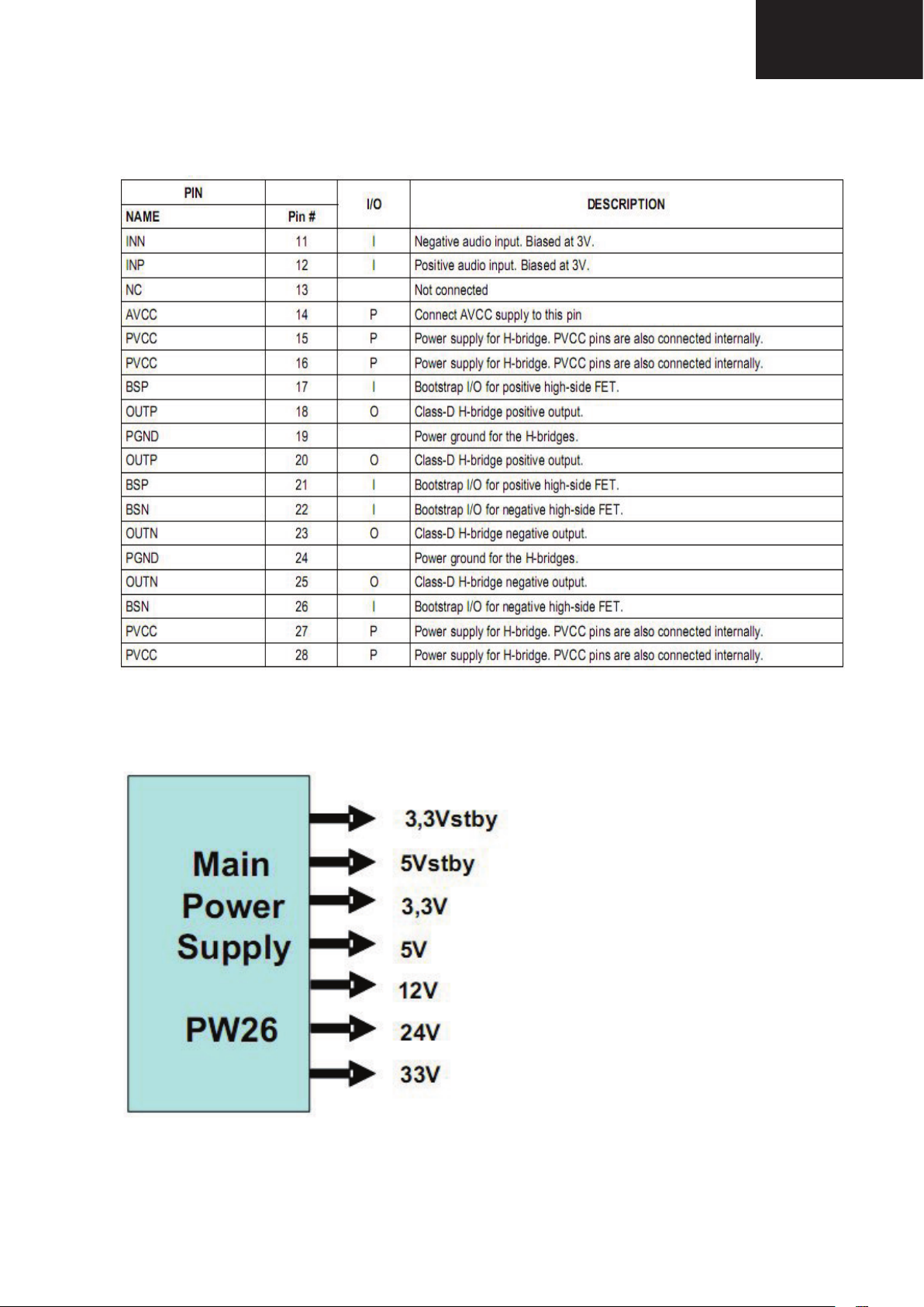
LC-32LE511
LC-40LE511
LC-40LE531
4. POWER STAGE
LC-32LE511
LC-40LE511
LC-40LE531
17MB70 general power managment
block diagram is shown below.
17PW26 power board is used in 32”
17MB70 TV sets.
3,3V stby, 5V stby, 3,3V, 5V, 12V,
24V and 33V can be generated by
PW26.
29
Below blocks are generated by stepdowns and regulators on MB70
board.
Page 30
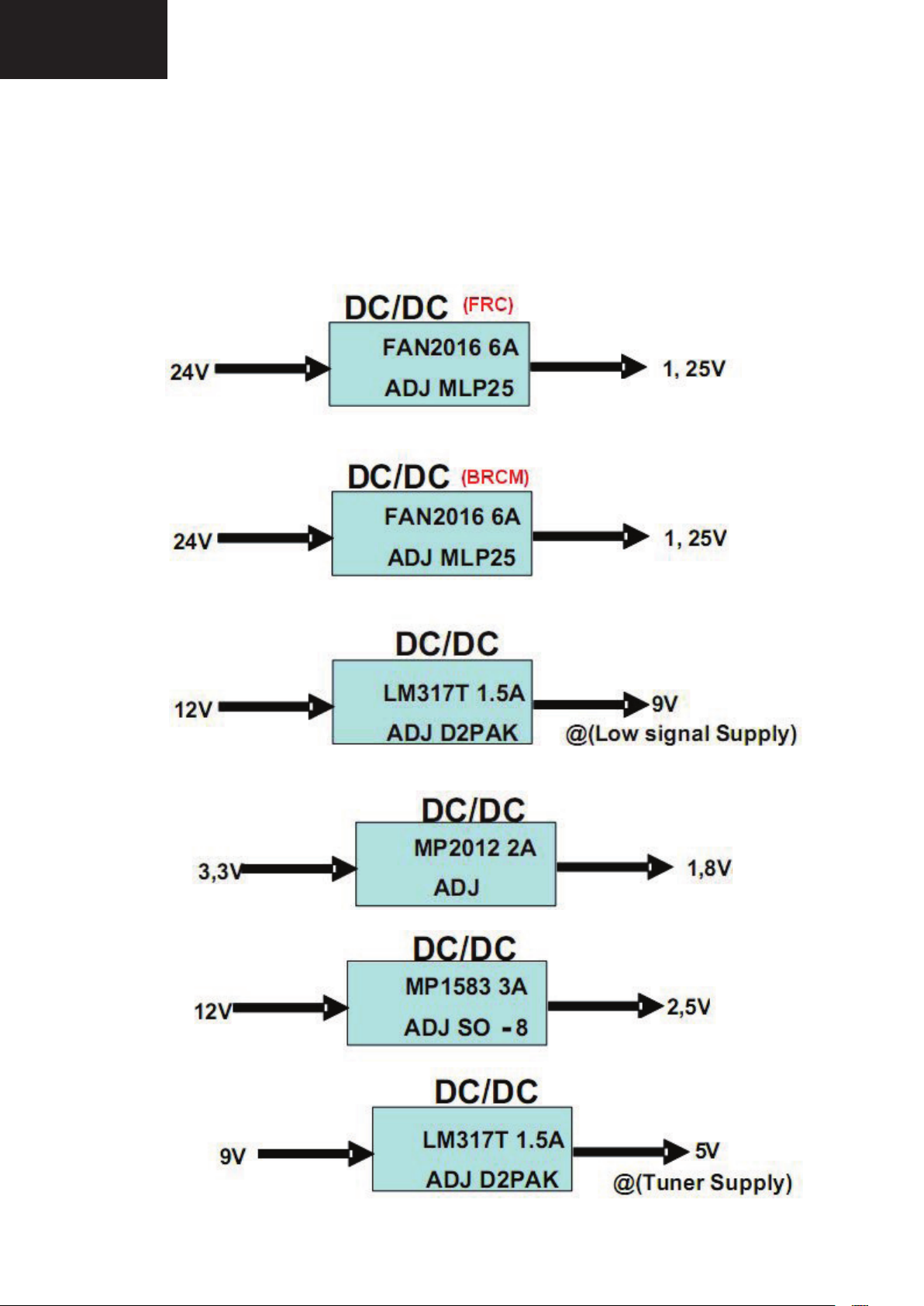
LC-32LE511
LC-40LE511
LC-40LE531
Power Blocks on MB70:
Below blocks are generated by step-downs and regulators on MB70 board.
30
Page 31

FAIRCHILD FAN2110 (U19-U20)
a) General Description
LC-32LE511
LC-40LE511
LC-40LE531
LC-32LE511
LC-40LE511
LC-40LE531
31
Page 32

LC-32LE511
.
LC-40LE511
LC-40LE531
Pin Configuration
Figure 3. MLP 5x6mm Pin Configuration (Bottom View)
Pin Definitions
Pin # Name Description
P1, 6-12 SW
P2, 2-5 VIN
P3, 21-23 PGND
1 BOOT
13 PGOOD
14 EN
15 VCC
16 AGND
17 ILIM
18 R(T)
19 FB
20 COMP
24 NC
25 RAMP
Switching Node. Junction of high-side and low-side MOSFETs.
Power Input Voltage. Connect to the main input power source.
Power Ground. Power return and Q2 source.
High-Side Drive BOOT Voltage. Connect through capacitor (C
includes an internal synchronous bootstrap diode to recharge the capacitor on this pin to
V
when SW is LOW.
CC
Power-Good Flag. An open-drain output that pulls LOW when FB is outside the limits
specified in electrical specs. PGOOD does not assert HIGH until the fault latch is enabled.
ENABLE. Enables operation when pulled to logic HIGH or left open. Toggling EN resets the
regulator after a latched fault condition. This input has an internal pull-up when the IC is
functioning normally. When a latched fault occurs, EN is discharged by a current sink.
Input Bias Supply for IC. The IC’s logic and analog circuitry are powered from this pin.
This pin should be decoupled to AGND through a >1µF X5R/X7R capacitor.
Analog Ground. The signal ground for the IC. All internal control voltages are referred to
this pin. Tie this pin to the ground island/plane through the lowest impedance connection.
Current Limit. A resistor (R
limit trip threshold lower than the default setting.
Oscillator Frequency. A resistor (R
frequency.
Output Voltage Feedback. Connect through a resistor divider to the output voltage.
Compensation. Error amplifier output. Connect the external compensation network
between this pin and FB.
No Connect. This pin is not used.
Ramp Amplitude. A resistor (R
amplitude and provides voltage feedforward functionality.
) to SW. The IC
BOOT
) from this pin to AGND can be used to program the current-
ILIM
) from this pin to AGND sets the PWM switching
T
) connected from this pin to VIN sets the ramp
RAMP
32
Page 33

LC-32LE511
.
LC-40LE511
LC-40LE531
Absolute Maximum Ratings
Stresses exceeding the absolute maximum ratings may damage the device. The device may not function or be
operable above the recommended operating conditions and stressing the parts to these levels is not recommended.
In addition, extended exposure to stresses above the recommended operating conditions may affect device
reliability. The absolute maximum ratings are stress ratings only.
Parameter Conditions Min. Max. Unit
VIN to PGND 28 V
VCC to AGND AGND = PGND 6 V
BOOT to PGND 35 V
BOOT to SW -0.3 6.0 V
SW to PGND
All other pins -0.3 VCC+0.3 V
ESD
Continuous -0.5 24.0
Transient (t < 20ns, f <
Human Body Model, JEDEC JESD22-A114 2.0
Charged Device Model, JEDEC JESD22-C101 2.5
600KHz) -5.0 30.0
V
kV
Recommended Operating Conditions
The Recommended Operating Conditions table defines the conditions for actual device operation. Recommended
operating conditions are specified to ensure optimal performance to the datasheet specifications. Fairchild does not
recommend exceeding them or designing to absolute maximum ratings.
Symbol Parameter Conditions Min. Typ. Max. Unit
VCC Bias Voltage VCC to AGND 4.5 5.0 5.5 V
VIN Supply Voltage VIN to PGND 3 24 V
TA Ambient Temperature
TJ Junction Temperature +125 °C
fSW Switching Frequency 200 600 KHz
FAN2106MPX -10 +85
FAN2106EMPX -40 +85
°C
Thermal Information
Symbol Parameter Min. Typ. Max. Unit
T
Storage Temperature -65 +150 °C
STG
TL Lead Soldering Temperature, 10 Seconds +300 °C
P1 (Q2) 4
JC
J-PCB
PD Power Dissipation, TA = 25°C 2.8
Note:
1. Typical thermal resistance when mounted on a four-layer, two-ounce PCB, as shown in Figure 26. Actual results
are dependent on mounting method and surface related to the design.
Thermal Resistance: Junction-to-Case
Thermal Resistance: Junction-to-Mounting Surface 35
P2 (Q1) 7
P3 4
(1)
°C/W
°C/W
(1)
W
LC-32LE511
LC-40LE511
LC-40LE531
MP1583 (U38)
.
DESCRIPTION
The MP1583 is a step-down regulator with abuilt-in internal Power MOSFET. It achieves 3A
of continuous output current over a wide input supply range with excellent load and line
regulation.
Current mode operation provides fast transient response and eases loop stabilization.
33
Page 34

LC-32LE511
LC-40LE511
LC-40LE531
Fault condition protection includes cycle-by-cycle current limiting and thermal shutdown. An
adjustable soft-start reduces the stress on the input source at startup. In shutdown mode the
regulator draws 20µA of supply current. The MP1583 requires a minimum number of
external components, providing a compact solution.
FEATURES
• 3A Output Current
• Programmable Soft-Start
• 100m
• Stable with Low ESR Output Ceramic Capacitors
• Up to 95% Efficiency
• 20µA Shutdown Mode
• Fixed 385KHz Frequency
• Thermal Shutdown
• Cycle-by-Cycle Over Current Protection
• Wide 4.75V to 23V Operating Input Range
• Output Adjustable from 1.22V to 21V
• Under-Voltage Lockout
MP2012 (U39)
The MP2012 is a fully integrated, internally compensated 1.2MHz fixed frequency PWM
step-down converter. It is ideal for powering portable equipment that runs from a single cell
Lithium-Ion (Li+) Battery, with an input range from 2.7V to 6V. The MP2012 can provide up
to 1.5A of load current with output voltage as low as 0.8V. It can also operate at 100% duty
34
Page 35

LC-32LE511
LC-40LE511
LC-40LE531
cycle for low dropout applications. With peak current mode control and internal
compensation, the MP2012 is stable with ceramic capacitors and small inductors. Fault
condition protection includes cycle-by-cycle current limiting and thermal shutdown. MP2012
is available in the small 6-pin 3mmx3mm QFN package.
2.7-6V Input Operation Range
Output Adjustable from 0.8V to VIN
Up to 95% Efficiency
100% Duty Cycle for Low Dropout Applications
1.2MHz Fixed Switching Frequency
Stable with Low ESR Output Ceramic Capacitors
Thermal Shutdown
Cycle-by-Cycle Over Current Protection
Short Circuit Protection
Available in 6-pin 3x3mm QFN
LC-32LE511
LC-40LE511
LC-40LE531
LM1117 (U21-U22-U23-U24)
35
Page 36

LC-32LE511
LC-40LE511
LC-40LE531
BCM3556
The BCM3556 is the next generation of System-on-a-Chip (SoC) Digital Television (DTV)
products from Broadcom® with 1080p60 input and output capability targetedfor the EU
Market. It combines a high level of integration with best-of-class picture quality, enabling TV
manufacturers to reduce overall system cost (BOM) and improve picture quality, all with a
single SoC.
The BCM3556 combines DVB-T COFDM terrestrial and PAL/SECAM demodulators, two
DVI/HDMI receivers, a transport processor, a digital audio processor, 3D/2D graphics
processing, Ethernet MAC and PHY, digital processing of analog video and audio, analog
video digitizer and DAC functions, stereo high-fidelity audio DACs, a 400-MHz dualthreaded MIPS processor, and a peripheral control unit providing a variety of television
control functions. The BCM3556 also features an advanced video decoder
capable of supporting high-definition AVC, VC-1, and DVB-T MPEG-2 streams.
5. MICROCONTROLLER(Broadcom)
a) General Description
The integration of the DVB-T COFDM terrestrial demodulator reduces the overall cost of the
external tuner module, resulting in cost savings for the customer. The BCM3556also
integrates four 10-bit ADCs with integrated front-end analog muxing that accept four CVBS
inputs, three S-video inputs, three component inputs, one PC input, one full SCART input
with fast blanking, and one Sound IF (SIF) input at the same time without the requirement for
any off-chip muxing ICs. The BCM3556 offers two HDMI 1.3a receivers, a motion adaptive
deinterlacer, HD Analog Noise Reduction, and an analog video decoder with 3D comb for
PAL and Y/C separation for SECAM.
The multiformat video decoder in the BCM3556 is capable of supporting high-definition
AVC, VC-1, and DVB-T MPEG-2 streams. AVC support is up to High Profile Level 4.1.
New tools in the AVC Fidelity Range extensions are supported, including 8x8 transform and
spatial prediction modes and adaptive quantization matrix. The video decoder also supports
high-definition VC-1 (Advanced Profile Level 3, Main, and Simple profiles) and DVBTcompliant MPEG-2, Main Profile at Main and High Levels. The BCM3556 has an advanced
programmable audio processor capable of decoding a broad range of formats including Dolby
Digital, Dolby Digital Plus, AAC 5.1, AAC+ Level 2, AAC+ Level 4, WMA, and MPEG-1
Layer 1, 2, and 3 with simultaneous pass-through support.
The BCM3556 also supports 3D SRS Audio and includes an analog audio decoder for BTSC
and A2 formats. The BCM3556 also integrates an analog audio switch that accepts six stereo
inputs. In addition, the SoC supports SPDIF and I2S inputs. One SPDIF, two I2S, and three
analog audio outputs are available.
The SoC family also has an integrated advanced Picture Enhancement Processor (PEP) to
improve sharpening and perform picture post-processing functions (e.g., autoflesh, green
boost, black and blue stretch). The PEP engine is fully programmable and can be optimized
by the TV manufacturer to meet their respective quality requirements. Also integrated is a
video encoder for NTSC and an advanced 2D/3D graphics for OSD acceleration.
36
Page 37

LC-32LE511
LC-40LE511
LC-40LE531
The BCM3556 supports direct PC inputs up to UXGA 1600x1200 formats with autophase
and automode detection and supports dual LVDS outputs to support 1080p60 panels.
The BCM3556 integrates a 400-MHz 32-bit MIPS dual CPU with two 32-KB
instructioncaches and a combined 64-KB data cache with a 128-KB L2 cache, and a 32-bit
800/1066-MHz DDR2. The BCM3556 also supports an 8-bit external NAND Flash interface
and SPI Flash interface for booting. Integrated peripherals include two USB2.0 ports, three
UARTs, controllers for SPI, BSC, keypad, LED and IR Tx/Rx, and an Ethernet port with
MAC and integrated PHY.
The BCM3556 is available in several package options: WXGA and FHD, PIP and non-PIP, or
MPEG-only and combined AVC/MPEG-2.
b) Features
• Advanced multiformat decoder supporting the following:
- H.264/AVC Main and High Profile to Level 4.1 (HD), Level 3.1 (SD)
- HD/SD AVS Jizhun Profile Levels 2.0, 4.0, and 6.0
- VC-1 Advanced Profile @ Level 3, simple and main profiles
- HD/SD MPEG-2 Main Profile at Main and High levels
- MPEG still image decode
- HD DivX® 3.11/4.11/5.x/6x/Home Theater
• 3D/2D OpenGL® ES 1.0- compliant graphics core
• Integrated Video Processing:
- 3D Color management
- Digital, Analog, and Mosquito Noise Reduction
- 1080i motion adaptive deinterlacing with 3:2/2:2 pull-down
- True 10-bit video carried through system
• Dual HDMI 1.3a receivers
• Extensive audio support:
- AAC+ Level 2, AAC-HE
- Dolby® Digital, Dolby Digital Plus, Trusurround XT®
- MPEG I layers 1, 2, and 3 (MP3)
- Windows Media® and Windows Media Pro audio
- Audio DACs, input switch, and equalizer
• Ethernet MAC and PHY
• Integrated DVB-T COFDM terrestrial demodulator:
- Standards compliance: ETSI EN 300 744, Nordig Unified v1.0.3, DTG D-Book 5
compliant
- Excellent Doppler performance
- Active impulse noise suppression
• Integrated PAL/SECAM Demodulator
• PAL decoder with a 3D/2D comb
• Direct PC input support up to 1600 x 1200 UXGA
• Integrated dual-link LVDS transmitters
• Dual USB 2.0
• A 400-MHz 32-bit MIPS dual CPU with two 32-KB instruction caches and a combined 64
KB data cache with 128-KB L2 cache
LC-32LE511
LC-40LE511
LC-40LE531
37
Page 38

LC-32LE511
LC-40LE511
LC-40LE531
c) BCM3556 - Block Diagram
38
Page 39

LC-32LE511
LC-40LE511
LC-40LE531
6. VIDEO BACK-END PROCESSOR (Trident)
PNX5120EH
a) General Description
The PNX5120EH is an advanced video picture improvement IC and the world's first solution,
NXP’s Motion Accurate Picture Processing (MAPP), to combine movie judder cancellation,
motion sharpness and vivid color management in a single device. Aimed primarily at digital
and hybrid flat panel televisions in the mid-end and high-end European,Asian and U.S.
consumer markets, it complies with relevant industry standards.LCD TVs represent a huge
and growing market, and the PNX5120EH offers manufacturers a unique combination of
richer color, dynamic motion, sensational sharpness, deep contrast, and full HD resolution.
Moreover, you can easily tailor that balance via the Automatic Picture Control tool (delivered
by NXP as part of a separate System Design-in Toolkit) to meet your own image quality
requirements.
b) Features
LC-32LE511
LC-40LE511
LC-40LE531
Single 27 MHz crystal clock input for all internal generated clocks
Three TriMedia TM3271 400 MHz, 32-bit VLIW media-processing cores with:
o five instructions per clock cycle
o 32 kB instruction cache
o 64 kB data cache
Integrated DDR2 SDRAM controller, 32-bit wide, up to 366 MHz clock (DDR2-800),
supporting 32 MB, 64 MB, 128 MB, and 256 MB single-rank memory configurations
Separately licensed, the PNX5120EH comes with an easy-to-use System Design-in
Toolkit (SDT), which includes the NXP Picture Quality Tuning Tool, firmware image
containing the NXP proprietary Picture Improvement features, and GPL-licensed UBoot Bootloader software.
DDR2-400 to DDR2-800 data rates supported
PCI/XIO (V2.2) operating at 33 MHz
Two UARTs
Two I2C DMA interfaces (100 kHz/400 kHz); the second I2C can be used as a
debugging interface
16 GPIO pins
Five PWM outputs
Support for 8-bit NOR flash up to 64 MB
Support for 8-bit/16-bit NAND flash up to 128 MB
c) PNX5120EH - Block Diagram
39
Page 40

LC-32LE511
LC-40LE511
LC-40LE531
7. FPGA (Spartan-3E)
XC3S1200E
a) General Description
The Spartan™-3E family of Field-Programmable Gate Arrays (FPGAs) is specifically
designed to meet the needs of high volume, cost-sensitive consumer electronic applications.
The five-member family offers densities ranging from 100,000 to 1.6 million system gates,
40
Page 41

The Spartan-3E family builds on the success of the earlier Spartan-3 family by increasing the
amount of logic per I/O, significantly reducing the cost per logic cell. New features
improve system performance and reduce the cost of configuration. These Spartan-3E
enhancements, combined with advanced 90 nm process technology, deliver more
functionality and bandwidth per dollar than was previously possible, setting new standards in
the programmable logic industry. Because of their exceptionally low cost, Spartan-3E FPGAs
are ideally suited to a wide range of consumer electronics applications, including broadband
access, home networking, display/projection, and digital television equipment. The Spartan3E family is a superior alternative to mask programmed ASICs. FPGAs avoid the high initial
cost, the lengthy development cycles, and the inherent inflexibility of conventional ASICs.
Also, FPGA programmability permits design upgrades in the field with no hardware
replacement necessary, an impossibility with ASICs.
b) Features
LC-32LE511
LC-40LE511
LC-40LE531
• Very low cost, high-performance logic solution for high-volume, consumer-oriented
applications
• Proven advanced 90-nanometer process technology
• Multi-voltage, multi-standard SelectIO™ interface pins
- Up to 376 I/O pins or 156 differential signal pairs
- LVCMOS, LVTTL, HSTL, and SSTL single-ended signal standards
- 3.3V, 2.5V, 1.8V, 1.5V, and 1.2V signaling
- 622+ Mb/s data transfer rate per I/O
- True LVDS, RSDS, mini-LVDS, differential HSTL/SSTL differential I/O
- Enhanced Double Data Rate (DDR) support
- DDR SDRAM support up to 333 Mb/s
• Abundant, flexible logic resources
- Densities up to 33,192 logic cells, including optional shift register or distributed
RAM support
- Efficient wide multiplexers, wide logic
- Fast look-ahead carry logic
- Enhanced 18 x 18 multipliers with optional pipeline
- IEEE 1149.1/1532 JTAG programming/debug port
• Hierarchical SelectRAM™ memory architecture
- Up to 648 Kbits of fast block RAM
- Up to 231 Kbits of efficient distributed RAM
• Up to eight Digital Clock Managers (DCMs)
- Clock skew elimination (delay locked loop)
- Frequency synthesis, multiplication, division
- High-resolution phase shifting
- Wide frequency range (5 MHz to over 300 MHz)
• Eight global clocks plus eight additional clocks per each half of device, plus abundant lowskew routing
• Configuration interface to industry-standard PROMs
- Low-cost, space-saving SPI serial Flash PROM
- x8 or x8/x16 parallel NOR Flash PROM
- Low-cost Xilinx Platform Flash with JTAG
• Complete Xilinx ISE™ and WebPACK™ development system support
• MicroBlaze™ and PicoBlaze™ embedded processor cores
• Fully compliant 32-/64-bit 33 MHz PCI support
LC-32LE511
LC-40LE511
LC-40LE531
41
Page 42

LC-32LE511
LC-40LE511
LC-40LE531
• Low-cost QFP and BGA packaging options
Samsung K4T1G084QF
- Common footprints support easy density migration
- Pb-free packaging options
8. 1Gb F-die DDR2-1066 SDRAM (U41-U42-U8-U9)
a) Key Features
• JEDEC standard VDD = 1.8V ± 0.1V Power Supply
•VDDQ = 1.8V ± 0.1V
• 533MHz fCK for 1066Mb/sec/pin
• 8 Banks
• Posted CAS
• Programmable CAS Latency: 4, 5, 6, 7
• Programmable Additive Latency: 3, 4, 5. 6
• Write Latency(WL) = Read Latency(RL) -1
• Burst Length: 4 , 8(Interleave/nibble sequential)
• Programmable Sequential / Interleave Burst Mode
• Bi-directional Differential Data-Strobe (Single-ended data-strobe is an optional feature)
• Off-Chip Driver(OCD) Impedance Adjustment
• On Die Termination
• Special Function Support
- PASR(Partial Array Self Refresh)
- 50ohm ODT
- High Temperature Self-Refresh rate enable
• Average Refresh Period 7.8us at lower than TCASE 85°C, 3.9us at 85°C < TCASE < 95 °C
• All of products are Lead-free, Halogen-free, and RoHS compliant
The 1Gb DDR2 SDRAM is organized as a 16Mbit x 8 I/Os x 8 banks, 8Mbit x 16 I/Os x 8
banks device. This synchronous device achieves high speed double-data-rate transfer rates of
up to 1066Mb/sec/pin (DDR2-1066) for general applications.
The chip is designed to comply with the following key DDR2 SDRAM features such as
posted CAS with additive latency, write latency = read latency - 1, Off-Chip Driver(OCD)
impedance adjustment and On Die Termination. All of the control and address inputs are
synchronized with a pair of externally supplied differential clocks. Inputs are latched at the
crosspoint of differential clocks (CK rising and CK falling). All I/Os are synchronized with a
pair of bidirectional strobes (DQS and DQS) in a source synchronous fashion. The address
42
Page 43

bus is used to convey row, column, and bank address information in a RAS/CAS
multiplexing style. For example, 1Gb(x8) device receive 14/10/3 addressing.
The 1Gb DDR2 device operates with a single 1.8V ± 0.1V power supply and 1.8V ± 0.1V
VDDQ.
The 1Gb DDR2 device is available in 60ball FBGA(x8) and 84ball FBGA(x16).
b) Pinning
LC-32LE511
LC-40LE511
LC-40LE531
8.1
LC-32LE511
LC-40LE511
LC-40LE531
c) Electrical Characteristics
43
Page 44

LC-32LE511
LC-40LE511
LC-40LE531
9. 32M x 16 bit DDRII Synchronous DRAM (U28-U29)
EtronTech EM68B16CWPA
a) Key Features
• JEDEC Standard Compliant
• JEDEC standard 1.8V I/O (SSTL_18-compatible)
• Power supplies: VDD & VDDQ = +1.8V ± 0.1V
• Operating temperatue: 0 – 85 °C
• Supports JEDEC clock jitter specification
• Fully synchronous operation
• Fast clock rate: 333/400MHz
• Differential Clock, CK & CK#
• Bidirectional single/differential data strobe
-DQS & DQS#
• 4 internal banks for concurrent operation
• 4-bit prefetch architecture
• Internal pipeline architecture
• Precharge & active power down
• Programmable Mode & Extended Mode registers
• Posted CAS# additive latency (AL): 0, 1, 2, 3, 4, 5
• WRITE latency = READ latency - 1 tCK
• Burst lengths: 4 or 8
• Burst type: Sequential / Interleave
• DLL enable/disable
• Off-Chip Driver (OCD)
-Impedance Adjustment
-Adjustable data-output drive strength
• On-die termination (ODT)
• RoHS compliant
• Auto Refresh and Self Refresh
• 8192 refresh cycles / 64ms
• Package: 84-ball 10x12.5x1.2mm (max) FBGA
- Pb and Halogen Free
44
Page 45

The EM68B16C is a high-speed CMOS Double-Data-Rate-Two (DDR2), synchronous
dynamic random-access memory (SDRAM) containing 512 Mbits in a 16-bit wide data I/Os.
It is internally configured as a quad bank DRAM, 4 banks x 8Mb addresses x 16 I/Os The
device is designed to comply with DDR2 DRAM key features such as posted CAS# with
additive latency, Write latency = Read latency -1, Off-Chip Driver (OCD) impedance
adjustment, and On Die Termination(ODT). All of the control and address inputs are
synchronized with a pair of externally supplied differential clocks. Inputs are latched at the
cross point of differential clocks (CK rising and CK# falling) All I/Os are synchronized with a
pair of bidirectional strobes (DQS and DQS#) in a source synchronous fashion. The address
bus is used to convey row, column, and bank address information in RAS #, CAS#
multiplexing style. Accesses begin with the registration of a Bank Activate command, and
then it is followed by a Read or Write command. Read and write accesses to the DDR2
SDRAM are 4 or 8-bit burst oriented; accesses start at a selected location and continue for a
programmed number of locations in a programmed sequence. Operating the four memory
banks in an interleaved fashion allows random access operation to occur at a higher rate than
is possible with standard DRAMs. An auto precharge function may be enabled to provide a
self-timed row precharge that is initiated at the end of the burst sequence. A sequential and
gapless data rate is possible depending on burst length, CAS# latency, and speed grade of the
device.
b) Pinning
LC-32LE511
LC-40LE511
LC-40LE531
LC-32LE511
LC-40LE511
LC-40LE531
45
Page 46

LC-32LE511
LC-40LE511
LC-40LE531
ST NAND04G-B2D
10. 4Gbit NAND Flash Memory (U35)
a) Key Features
– Up to 8 Gbit memory array
– Cost-effective solution for mass storage
applications
– x8 or 16x bus width
– Multiplexed address/data
– x8 device: (2048 + 64 spare) bytes
– x16 device: (1024 + 32 spare) words
– x8 device: (128K + 4 K spare) bytes
– x16 device: (64K + 2 K spare) words
– Array split into two independent planes
– Program/erase operations can be
performed on both planes at the same time
– Random access: 25 µs (max)
– Sequential access: 25 ns (min)
– Page program time: 200 µs (typ)
– Multiplane page program time (2 pages):
200 µs (typ)
detection code (EDC)
– Block erase time: 1.5 ms (typ)
– Multiblock erase time (2 blocks):
1.5 ms (typ)
– Up to 8 Gbit memory array
– Cost-effective solution for mass storage
applications
face
– x8 or 16x bus width
– Multiplexed address/data
– x8 device: (2048 + 64 spare) bytes
– x16 device: (1024 + 32 spare) words
– x8 device: (128K + 4 K spare) bytes
– x16 device: (64K + 2 K spare) words
– Array split into two independent planes
– Program/erase operations can be
performed on both planes at the same time
– Random access: 25 µs (max)
– Sequential access: 25 ns (min)
– Page program time: 200 µs (typ)
– Multiplane page program time (2 pages):
200 µs (typ)
detection code (EDC)
– Block erase time: 1.5 ms (typ)
– Multiblock erase time (2 blocks):
1.5 ms (typ)
n
46
Page 47

b) Pinning
LC-32LE511
LC-40LE511
LC-40LE531
LC-32LE511
LC-40LE511
LC-40LE531
47
Page 48

LC-32LE511
LC-40LE511
LC-40LE531
11. 128Mbit NAND Flash Memory (U17)
ST NAND128-A
a) Key Features
MEMORIES
– Up to 1 Gbit memory array
– Up to 32 Mbit spare area
– Cost effective solutions for mass storage
applications
– x8 or x16 bus width
– Multiplexed Address/ Data
– Pinout compatibility for all densities
– 1.8V device: VDD = 1.7 to 1.95V
– 3.0V device: VDD = 2.7 to 3.6V
– x8 device: (512 + 16 spare) Bytes
– x16 device: (256 + 8 spare) Words
– x8 device: (16K + 512 spare) Bytes
– x16 device: (8K + 256 spare) Words
– Random access: 12µs (max)
– Sequential access: 50ns (min)
– Page program time: 200µs (typ)
– Fast page copy without external
buffering
– Block erase time: 2ms (Typ)
OPTION
– Simple interface with microcontroller
– Program/Erase locked during Power
Transitions
– 100,000 Program/Erase cycles
– 10 years Data Retention
– Lead-Free Components are Compliant
with the RoHS Directive
– Error Correction Code software and
hardware models
– Bad Blocks Management and Wear
Leveling algorithms
– File System OS Native reference
software
– Hardware simulation models
b) Pinning
48
Page 49

LC-32LE511
LC-40LE511
LC-40LE531
V
V
NC
NC
NC
NC
NC
NC
RB
NC
NC
DD
SS
NC
NC
CL
AL
WP
NC
NC
NC
NC
NC
1
R
E
NAND Flash
12
13
W
24 25
(x8)
48
37
36
NC
NC
NC
NC
I/O7
I/O6
I/O5
I/O4
NC
NC
NC
V
DD
V
SS
NC
NC
NC
I/O3
I/O2
I/O1
I/O0
NC
NC
NC
NC
V
V
NC
NC
NC
NC
NC
NC
RB
NC
NC
DD
SS
NC
NC
CL
AL
W
WP
NC
NC
NC
NC
NC
1
R
E
NAND Flash
12
13
24 25
(x16)
48
37
36
V
SS
I/O15
I/O7
I/O14
I/O6
I/O13
I/O5
I/O12
I/O4
NC
NC
V
DD
NC
NC
NC
I/O11
I/O3
I/O10
I/O2
I/O9
I/O1
I/O8
I/O0
V
SS
LC-32LE511
LC-40LE511
LC-40LE531
AI07585B
12. USB Interface
USB ports are directly connected concept IC, BCM 3556.
USB ciecuit has 2 main parts:
Protection IC (U4)
Over Curent Protection IC (U108-U109)
AI07559B
49
Page 50

LC-32LE511
LC-40LE511
LC-40LE531
17MB70 Digital CI ve Smart Card Interface Block diagram:
13. CI Interface
14. DVB-C/T2 Demodulator
Sony CXD2820R
a) Key Features
DESCRIPTION
The Sony CXD2820R is a combined DVB-T2, DVB-T and DVB-C demodulator that
conforms to the ETSI EN 302-755 (second generation Terrestrial) ETSI EN 300-744
(Terrestrial) and ETSI EN 300-429 (Cable) standards.
The CXD2820R is a DVB-T2 demodulator offering class-leading performance, optimised
BOM requiring no external memory and low processor overhead. It includes a highly
integrated dual-core DVB-T and DVB-C demodulator which complies with all relevant
European performance standards.
FEATURES DVB-T2
• Supports all DVB-T2 modes, including
• Single and multiple-PLPs
• SISO and MISO transmission
• Simple API
• Fully-automatic acquisition
• Fully-automatic L1-signalling decoding
• Automatic guard-interval detection
• Automatically-calculated constant-rate TS output (using L1
signalling and ISSY)
• Acquisition range ±857kHz
50
Page 51

• Stream processor for automatic common- and data-PLP combination
• Null-packet insertion
• Access to channel echo profile and constellation via I2C
FEATURES DVB-C
• Wide symbol range, 0.7 to 7.2Msym/s
• Integrated matched filter 0.15 roll-off factor
• Auto Acquisition controller with fast re-acquisition mode, 15ms typ.
• Programmable acquisition range ±500kHz
• 2.8us echo cancellation at 7.2Msym/s
• Low impl. loss 0.4dB @ 64QAM and <1.0dB @ 256QAM typ.
• Enhanced channel scanning performance through improved rejection of non-digital signals
• Access to channel SNR, constellation data and dynamic equaliser tap values via I2C
APPLICATIONS
• Set Top Boxes
• IDTV with Digital only or Hybrid Tuner Support
• PC TV
• PVRs and recordable DVD players
• Test equipment
LC-32LE511
LC-40LE511
LC-40LE531
LC-32LE511
LC-40LE511
LC-40LE531
GENERAL FEATURES
• Single, 41MHz crystal (can be shared with CXD2813R analogue demod IC)
• High performance differential signal ADC
• RF power level monitor ADC
• Low IF and high IF (36MHz) mode input
• Fast 400kHz I2C compatible bus interface
• Quiet I2C interface for dedicated tuner control
• Automatic IF AGC and optional programmable
RF AGC/GPIO functions
• Configurable parallel and serial MPEG-2 TS outputs with smoothing buffer
• 3.3V, 2.5V, 1.2V supplies
• Temperature range -20°C to +85°C
• 64 pin exposed-pad LQFP 10mm x 10mm package
• Supplied with full reference design, including software driver, PCB schematic/layouts, GUI
and documentation
b) Block Diagram
51
Page 52

LC-32LE511
LC-40LE511
LC-40LE531
AIN P/
AINM
RFAIN
41MH z
IFA G C/
RFAGC
TUNERCLK
TUNERDAT
12 -bit
ADC
10 -bit
ADC
OSC
PLL
AGC
DV B-T2
Co re
DV B-T
Co re
DVB-C
Co re
LDPC/
BCH
Decoder
Vi terb i/
RS D ecoder
Stre am
Processor
TS
Smoothing
TS IF
I2C IF
TSCLK
TSVALID
TSSYNC
TSERR
TSDATA
SCL
SDA
c) Pinning
52
Page 53

LC-32LE511
LC-40LE511
LC-40LE531
GPIO0 1 I/O General purpose I/O
TSERR _GPIO2 2 O
TSSYNC 3 O TS sync flag
TSVALID 4 O TS valid flag
TSCLK 5 O TS clock output
VSS 6 Digital Ground n/a
CVDD 7
MVDD 8
MVSS 9 Digital Ground n/a
VSS 10 Digital Ground n/a
DVDD 11
TS error flag
General purpose I/O
1.2V digital power
supply
1.2V digital power
supply
3.3V digital power
supply
5V tolerant
Controllable pull-up
5V tolerant
Controllable pull-up
Controllable pull-up
Selectable output current
Controllable pull-up
Selectable output current
Controllable pull-up
Selectable output current
n/a
n/a Supplies memory power
n/a
LC-32LE511
LC-40LE511
LC-40LE531
TSDATA0 12 O TS data output
TSDATA1 13 O TS data output
CVDD 14
VSS 15 Digital Ground n/a
TSDATA2 16 O TS data output
TSDATA3 17 O TS data output
MVSS 18 Digital Ground n/a
MVDD 19
CVDD 20
VSS 21 Digital Ground n/a
1.2V digital power
supply
1.2V digital power
supply
1.2V digital power
supply
Controllable pull-up
Selectable output current
Controllable pull-up
Selectable output current
n/a
Controllable pull-up
Selectable output current
Controllable pull-up
Selectable output current
n/a Supplies memory power
n/a
53
Page 54

LC-32LE511
LC-40LE511
LC-40LE531
Name No. I/O Function Equivalent Circuit Note
TSDATA4 22 O TS data output
TSDATA5 23 O TS data output
TSDATA6 24 O TS data output
TSDATA7 25 O TS data output
VSS 26 Digital Ground n/a
DVDD 27
SCL 28 I I2C clock
SDA 29 I/O I2C data
3.3V digital power
supply
Controllable pull-up
Selectable output current
Controllable pull-up
Selectable output current
Controllable pull-up
Selectable output current
Controllable pull-up
Selectable output current
n/a
5V tolerant
5V tolerant
CVDD 30
VSS 31 Digital Ground n/a
TESTMODE 32 I Test mode setting
A0 33 I
OSCENBN 34 I Oscillator enable
VSS 35 Digital Ground n/a
CVDD 36
RESETN 37 I Hardware reset
OSCMODE 38 I
1.2V digital power
supply
2
I
C slave address
selection
1.2V digital power
supply
3rd overtone crystal
selection
n/a
5V tolerant
1: Test mode
0: Normal mode
5V tolerant
5V tolerant
1: Stop
0: Run
n/a
5V tolerant
5V tolerant
1: fundamental
0: 3rd overtone
MVSS 39 Digital Ground n/a
MVDD 40
MVDD 41 1.2V digital power n/a Supplies memory power
1.2V digital power
supply
n/a Supplies memory power
54
Page 55

Name No. I/O Function Equivalent Circuit Note
supply
MVSS 42 Digital Ground n/a
PVSS 43 Analog Ground n/a
PVDD 44
XVDD 45
XTALO 46 O Crystal oscillator output
1.2V analog power
supply
2.5V analog power
supply
n/a Supplies PLL power
n/a
Supplies crystal oscillator
power
Leave open when external
clock input to XTALI
LC-32LE511
LC-40LE511
LC-40LE531
XTALI 47 I Crystal oscillator input
XVSS 48 Analog Ground n/a
AINM 49 I IF input (-)
AINP 50 I IF input (+)
AVSS 51 Analog Ground n/a
AVDD 52
RFAIN 53 I RF level monitor
RVDD 54
VSS 55 Digital Ground n/a
CVDD 56
TUNERDAT 57 I/O Tuner I2C data
2.5V analog power
supply
3.3V digital power
supply (*1)
1.2V digital power
supply
External clock input pin
n/a Supplies IF ADC power
n/a
n/a
Supplies RF level monitor
ADC power
5V tolerant
LC-32LE511
LC-40LE511
LC-40LE531
TUNERCLK 58 O Tuner I2C clock
DVDD 59
VSS 60 Digital Ground n/a
CVDD 61
PLLBPN 62 I PLL bypass
RFAGC_GPIO1 63 I/O
IFAGC 64 O IFAGC output
3.3V digital power
supply
1.2V digital power
supply
RFAGC output
General purpose I/O
55
5V tolerant
n/a
n/a
5V tolerant
1: Use PLL
0: Bypass PLL
PWM output
5V tolerant
Controllable pull-up
CAUTION: intermediate
voltage input is prohibited.
PWM output
CAUTION: 5V input is
prohibited.
Page 56

LC-32LE511
LC-40LE511
LC-40LE531
NEC uPD78F0503
15. LOW POWER&CEC MICROCONTROLLER
Pinning
56
Page 57

CEC Circuit Design for CEC option:
LC-32LE511
LC-40LE511
LC-40LE531
1
2
3
4
U115
LM358D
OUT1
IN1-
IN1+
GND
VCC
OUT2
IN2-
IN2+
8
7
6
5
C922
10k
R1002
3V3_STBY
100n
R999
16V
3V3_STBY
R1003
12k
3V3_STBY
16. HDMI SWITCH
R1000
10k
12k
CEC_OUT
3V3_STBY
4k7
R996
C925
4n7
50V
R997
4k7
3V3_STBY
C924
47p
50V
C921
100n
16V
R1001
47k
R1007
470R
220R
R1006
27k
R1008
UC_CEC
D53
220R
R1005
1N4148
Q129
BC848B
CEC
LC-32LE511
LC-40LE511
LC-40LE531
Silicon Image SiI9287B
a) Key Features
x Four-input, single-output HDMI port processor
x Improved ESD protection on all signals connected to HDMI connector
x Integrated TMDS receiver and transmitter cores capable of receiving and transmitting at
2.25 Gbps:
x InstaPort™ viewing technology
x MHL support
x Supports video resolutions up to 1080p, 60 Hz, 12bit or 720p/1080i, 120 Hz, 12-bit
x Built-in adaptive equalizer provides long cable support even at Deep Color resolutions,
enabling the SiI9287B device to work with noisy signals and many sources, making the sink
devices highly interoperable
x Receiver fully complies with DVI 1.0, HDCP 1.3 and HDMI 1.3a specifications.
57
Page 58

LC-32LE511
LC-40LE511
LC-40LE531
b) Block Diagram
58
Page 59

LC-32LE511
LC-40LE511
LC-40LE531
LC-32LE511
LC-40LE511
LC-40LE531
Figure 8. Pin Diagram
59
Page 60

LC-32LE511
Pin Name
Type
LC-40LE511
LC-40LE531
R0X0P 68
R0X0N 67
R0X1P 70
R0X1N 69
R0X2P 72
R0X2N 71
R0XCP 66
R0XCN 65
R1X0P 4
R1X0N 3
R1X1P 6
R1X1N 5
R1X2P 8
R1X2N 7
R1XCP 2
R1XCN 1
R2X0P 14
R2X0N 13
R2X1P 16
R2X1N 15
R2X2P 18
R2X2N 17
R2XCP 12
R2XCN 11
R3X0P 22
R3X0N 21
R3X1P 24
R3X1N 23
R3X2P 26
R3X2N 25
R3XCP 20
R3XCN 19
Dir Description
TMDS Input TMDS input Port 0 data pair for HDMI and MHL.
TMDS Input TMDS input Port 0 data pairs for HDMI.
TMDS Input TMDS input Port 0 clock pair for HDMI and MHL.
TMDS Input TMDS input Port 1 data pair for HDMI and MHL.
TMDS Input TMDS input Port 1 data pairs for HDMI.
TMDS Input TMDS input Port 1 clock pair for HDMI and MHL.
TMDS Input TMDS input Port 2 data pair for HDMI and MHL.
TMDS Input TMDS input Port 2 data pairs for HDMI.
TMDS Input TMDS input Port 2 clock pair for HDMI and MHL.
TMDS Input TMDS input Port 3 data pair for HDMI and MHL.
TMDS Input TMDS input Port 3 data pairs for HDMI.
TMDS Input TMDS input Port 3 clock pair for HDMI and MHL.
HDMI Transmitter Port Pins
Signal Name Pin
TX0P 60
TX0N 61
TX1P 58
TX1N 59
TX2P 56
TX2N 57
TXCP 62
TXCN 63
TMDS Output HDMI Output Port Data.
TMDS Output HDMI Output Port Clock.
Dir Description
TMDS Low Voltage Differential Signal output data pairs.
TMDS Low Voltage Differential Signal output clock pair.
60
Page 61

Pin Name
Dir Description
R0X0P 68
R0X0N 67
TMDS Input TMDS input Port 0 data pair for HDMI and MHL.
R0X1P 70
R0X1N 69
R0X2P 72
R0X2N 71
TMDS Input TMDS input Port 0 data pairs for HDMI.
R0XCP 66
R0XCN 65
TMDS Input TMDS input Port 0 clock pair for HDMI and MHL.
R1X0P 4
R1X0N 3
TMDS Input TMDS input Port 1 data pair for HDMI and MHL.
R1X1P 6
R1X1N 5
R1X2P 8
R1X2N 7
TMDS Input TMDS input Port 1 data pairs for HDMI.
R1XCP 2
R1XCN 1
TMDS Input TMDS input Port 1 clock pair for HDMI and MHL.
R2X0P 14
R2X0N 13
TMDS Input TMDS input Port 2 data pair for HDMI and MHL.
R2X1P 16
R2X1N 15
R2X2P 18
R2X2N 17
TMDS Input TMDS input Port 2 data pairs for HDMI.
R2XCP 12
R2XCN 11
TMDS Input TMDS input Port 2 clock pair for HDMI and MHL.
R3X0P 22
R3X0N 21
TMDS Input TMDS input Port 3 data pair for HDMI and MHL.
R3X1P 24
R3X1N 23
R3X2P 26
R3X2N 25
TMDS Input TMDS input Port 3 data pairs for HDMI.
R3XCP 20
R3XCN 19
TMDS Input TMDS input Port 3 clock pair for HDMI and MHL.
HDMI Transmitter Port Pins
Signal Name Pin
Type
Dir Description
TX0P 60
TX0N 61
TX1P 58
TX1N 59
TX2P 56
TX2N 57
TMDS Output HDMI Output Port Data.
TMDS Low Voltage Differential Signal output data pairs.
TXCP 62
TXCN 63
TMDS Output HDMI Output Port Clock.
TMDS Low Voltage Differential Signal output clock pair.
Pin Name
Dir
recommended.
Pin Name
Dir
Pin Name
Dir
DSDA0
DSDA1
DSDA2
DSDA3
DSCL0
DSCL1
DSCL2
DSCL3
R0PWR5V
R1PWR5V
R2PWR5V
R3PWR5V
CBUS_HPD0
CBUS_HPD1
CBUS_HPD2
CBUS_HPD3
43
R4PWR5V 49 Power Input 5V Standby power or 5V power from 5th Receiver port.
CSCL 54
CSDA 53
DSCL4 48
DSDA4 47
TPWR_CI2CA 55
RSVDL
RSVDL
INT 52
Type
29
33
39
43
30
34
40
44
32
36
42
46
31
35
41
45
10
28
LVTTL
Schmitt
Open drain
5-V tolerant
Open drain
5-V tolerant
5-V tolerant
Type
Open drain
5-V tolerant
Open drain
5-V tolerant
5-V tolerant
5-V tolerant
5-V tolerant
Open drain
5-V tolerant
Reserved pin —
LVTTL
Schmitt
Power Input 5V Port detection input for respective port.
LVTTL
Schmitt
LVTTL
Schmitt
LVTTL
Schmitt
LVTTL
Schmitt
LVTTL
8 mA
Schmitt
8 mA
2
C Data for respective port.
Input
Output
Input DDC I
Output Hot Plug Detect Output for respective port.
Input Local Configuration/Status I
Input
Output
Input DDC I2C Clock for VGA port.
Input
output
Input
Output
Input
Output
DDC I
These signals are true open drain, and do not pull-down to ground when
power is not applied to the device. These pins require an external pull-up
resistor.
2
C Clock for respective port.
These signals are true open drain, and do not pull-down to ground when
power is not applied to the device. These pins require an external pull-up
resistor.
Connect to 5V signal from HDMI input connector. These signals require a
10 series resistor and at least a 1 PF capacitor to ground. A 100 k pulldown resistor is also required for these signals.
Connect to HOTPLUG of HDMI input connector. In MHL mode, this serves
as the respective port control bus.
If this signal is connected to the VGA cable then it requires a 10 ohm series
resistor and at least a 1 PF capacitor to ground. If connected to a local power
supply the resistor is not needed but a capacitor of at least 1 PF is
2
C Clock.
Chip configuration/status is accessed using this I
open drain, so it does not pull to ground if power is not applied.
Local Configuration/Status I
Chip configuration/status is accessed using this I
open drain, so it does not pull to ground if power is not applied.
These signals are true open drain, and do not pull-down to ground when
power is not applied to the device. This pin requires an external pull-up
resistor.
2
C Data for VGA port.
DDC I
These signals are true open drain, and do not pull-down to ground when
power is not applied to the device. This pin requires an external pull-up
resistor.
2
C Slave Address input / Transmit Power Sense Output.
I
At the end of power-on-reset (POR), this pin is used as an input to latch the
2
C sub-address. The level on this pin is latched when the POR transitions
I
from the asserted state to the de-asserted state. After completion of POR,
this pin is used as the TPWR output, indicating that the selected HDMI input
port is receiving an active TMDS clock. This pin has an internal pull-up to
the MICOMVCC33 power supply. If this signal is pulled-down, a 4.7K ohm
resistor should be used.
Interrupt Output.
This is an open-drain output and requires an external pull-up resistor.
These pins must be tied to ground with a 10 k or less resistor during
normal operation. Connecting directly to ground is recommended.
2
C Data.
LC-32LE511
LC-40LE511
LC-40LE531
2
C port. This pin is a true
2
C port. This pin is a true
LC-32LE511
LC-40LE511
LC-40LE531
61
Page 62

LC-32LE511
Pin Name
Type
Dir
CSDA 53
LVTTL
Schmitt
Open drain
5-V tolerant
Input
Output
Local Configuration/Status I
2
C Data.
Chip configuration/status is accessed using this I
2
C port. This pin is a true
open drain, so it does not pull to ground if power is not applied.
DSCL4 48
LVTTL
Schmitt
5-V tolerant
Input DDC I
2
C Clock for VGA port.
These signals are true open drain, and do not pull-down to ground when
power is not applied to the device. This pin requires an external pull-up
resistor.
DSDA4 47
LVTTL
Schmitt
5-V tolerant
Input
output
DDC I
2
C Data for VGA port.
These signals are true open drain, and do not pull-down to ground when
power is not applied to the device. This pin requires an external pull-up
resistor.
CSCL 54
Schmitt
Open drain
5-V tolerant
Input Local Configuration/Status I
2
C Clock.
Chip configuration/status is accessed using this I
2
C port. This pin is a true
open drain, so it does not pull to ground if power is not applied.
Pin Name
Dir
INT 52
Schmitt
Open drain
8 mA
5-V tolerant
Input
Output
Interrupt Output.
This is an open-drain output and requires an external pull-up resistor.
RSVDL
RSVDL
10
28
Reserved pin —
These pins must be tied to ground with a 10 k or less resistor during
normal operation. Connecting directly to ground is recommended.
TPWR_CI2CA 55
LVTTL
8 mA
5-V tolerant
Input
Output
I
2
C Slave Address input / Transmit Power Sense Output.
At the end of power-on-reset (POR), this pin is used as an input to latch the
I
2
C sub-address. The level on this pin is latched when the POR transitions
from the asserted state to the de-asserted state. After completion of POR,
this pin is used as the TPWR output, indicating that the selected HDMI input
port is receiving an active TMDS clock. This pin has an internal pull-up to
the MICOMVCC33 power supply. If this signal is pulled-down, a 4.7K ohm
resistor should be used.
Pin Name
Type
Signal Name
LC-40LE511
LC-40LE531
Pin Name
CEC_A 50
CEC_D 51
Power and Ground Pins
VCC33 9, 27, 64 Power Analog and digital core VCC. Must be supplied at 3.3 V.
MICOM_VCC33 37 Output
SBVCC33 38 Power
ePAD ePad Ground ePad must be connected to Ground.
Pin
CEC Compliant
5-V tolerant
Open drain
5-V tolerant
Direct
Description
ion
Input
Output
HDMI compliant CEC I/O used for interfacing to CEC devices.
This signal is electrically compliant with the CEC specification. It connects
to the CEC signal of all HDMI connectors in the system.
As an input, this pin acts as a LVTTL Schmitt triggered input and is 5-V
LVTTL
Schmitt
Input
Output
tolerant. As an output, the pin acts as an NMOS driver with resistive pull-up.
This pin has an internal pull-up resistor.
CEC interface to local system.
This pin is an open drain and requires an external pull-up resistor. This pin
typically connects to a local CPU if the CEC functions are performed by the
CPU directly, and not the CEC controller inside the device.
Type
During normal mode, this pin provides 3.3 V power to an external
microcontroller. The maximum output current is 30 mA. This pin
requires 1PF capacitor to ground.
3.3V standby power. If 3.3V standby mode is not used, this pin
should be left as not connected.
All analog and digital ground planes are tied together to the ePad,
which must be connected to Ground.
62
Page 63

17. LNB supply and control IC
ST LNBH23L
a) Key Features
-in DC-DC converter for single 12 V supply operation and high efficiency (typ. 93%
@0.5 A)
pecification
-in 22 kHz tone generator suits widely accepted standards
-drop post regulator and high efficiency step-up PWM with integrated power NMOS
allow low power losses
-temperature internal protections with I²C diagnostic bits
- 4 kV ESD tolerant on output power pins
LC-32LE511
LC-40LE511
LC-40LE531
LC-32LE511
LC-40LE511
LC-40LE531
Applications
te receivers
Description
Intended for analog and digital satellite receivers, the LNBH23L is a monolithic voltage
regulator and interface IC, assembled in QFN32 5 x 5 specifically designed to provide the 13 /
18 V power supply and the 22 kHz tone signalling to the LNB down-converter in the antenna
dish or to the multi-switch box. In this application field, it offers a complete solution with
extremely low component count, low power dissipation together with simple design and I²C
standard interfacing.
63
Page 64

LC-32LE511
LC-40LE511
LC-40LE531
b) Block Diagram
64
Page 65

b) Block Diagram
SOFWARE UPDATE
18. Software Update
18.1 Main SW update
LC-32LE511
LC-40LE511
LC-40LE531
In MB70 project you can update the main IC software by using USB ports. You can find the
SW update procedure below.
1. Software files should copy directly inside of a flash memory(not in a folder).
2. Put flash memory to the tv when tv is powered off.
3. Power on the and wait. TV will power-up itself.
4. If First Time Installition screen comes, it means software update procedure is succesful.
5. You can check the SW release name from service menu.
18.2 Panel Configuration File update
In MB70 project you can update the panel Configuration file by using USB ports. You can
find the update procedure below.
1. Please copy panel configuration files to USB root.
2. Turn power to OFF by remote controler and plug the USB to TV.
3. Turn power to ON by using remote controler.
4. TV standby led will blink rapidly during the sw update. Please wait approximately for 1-2
minutes.
5. TV will open automatically with the new panel configurations.
18.3 Stby-Microcontroller file update
18.3 Stby-Microntroller le update
LC-32LE511
LC-40LE511
LC-40LE531
1. Please copy Standby micro-controller file to USB root.
2. You have to use Service Menu for standby micro-controller files update.
3. To access the service menu push “menu” button and enter the password “4725” while
menu icons are on screen.
4. Plug the USB to TV.
5. Please choose “USB Operations” tab to update standby-micro sw file by using remote
controler.
6. Please wait approximately for 30 seconds
65
Page 66

LC-32LE511
18.3 Stby-Microcontroller file update
1. Please copy Standby micro-controller file to USB root.
2. You have to use Service Menu for standby micro-controller files update.
3. To access the service menu push “menu” button and enter the password “4725” while
menu icons are on screen.
4. Plug the USB to TV.
5. Please choose “USB Operations” tab to update standby-micro sw file by using remote
controler.
6. Please wait approximately for 30 seconds
To reach the latest sw files please use;
https://www.vestelservice.com/100359/New_Projects/Sharp/Sharp_2011/9_Customer
_support/SW/
LC-40LE511
LC-40LE531
Problem: If TV is working, led is normal and there is no picture and backlight on the panel.
Possible couses: Backlight pin, dimming pin, backlight supply, stby on/off pin
BACKLIGHT_ON/OFF pin should be high when the backlight is ON. R185 must be low
when the backlight is OFF. If it is a problem, please check Q131 and the panel cables.
TROUBLESHOOTING
19. Troubleshooting
A. No Backlight Problem
66
Page 67

LC-32LE511
LC-40LE511
LC-40LE531
LC-32LE511
LC-40LE511
LC-40LE531
Dimming pin should be high or square wave in open position. If it is low, please check S32
for BRCM side and panel or power cables, connectors.
67
Page 68

LC-32LE511
LC-40LE511
LC-40LE531
STBY_ON/OFF_NOT should be high for standby condition, please check R203.
68
Page 69

STBY_ON/OFF_NOT should be high for standby condition, please check R203.
B. CI Module Problem
Problem: CI is not working when CI module inserted.
Possible couses: Supply, suply control pin, detect pins, mechanical positions of pins.
CI supply should be 5V when CI module inserted. If it is not 5V please check
CI_PWR_CTRL, this pin should be low.
LC-32LE511
LC-40LE511
LC-40LE531
Please check mechanical position of CI module. Is it inserted properly or not?
LC-32LE511
LC-40LE511
LC-40LE531
Detect ports should be low. If it is not low please check CI connector pins, CI module
pins.
69
Page 70

LC-32LE511
LC-40LE511
LC-40LE531
C. Staying in Stand-by Mode
Problem: Staying in stand-by mode, no other operation
This problem indicates a short on Vcc voltages. Protect pin should be logic high while normal
operation. When there is a short circuit protect pin will be logic low. If you detect logic low
on protect pin, unplug the TV set and control voltage points with a multimeter to find the
shorted voltage to ground.
70
Page 71

LC-32LE511
LC-40LE511
LC-40LE531
LC-32LE511
LC-40LE511
LC-40LE531
D. IR Problem
Problem: LED or IR not working
Check LED card supply on MB70 chasis.
71
Page 72

LC-32LE511
LC-40LE511
LC-40LE531
E. Keypad Touchpad Problems
Problem: Keypad or Touchpad is not working
Check keypad supply on MB70.
72
Page 73

F. USB Problems
Problem: USB is not working or no USB Detection.
Check USB Supply, It should be nearly 5V. Also USB Enable should be logic high.
LC-32LE511
LC-40LE511
LC-40LE531
G. No Sound Problem
Problem: No audio at main TV speaker outputs.
Check supply voltages of VDD_AUDIO, 8V_VCC and 12V_VCC with a voltage-meter.
There may be a problem in headphone connector or headphone detect circuit (when
headphone is connected, speakers are automatically muted). Measure voltage at HP_DETECT
pin, it should be 3.3v.
LC-32LE511
LC-40LE511
LC-40LE531
H. Standby On/Off Problem
Problem: Device can not boot, TV hangs in standby mode.
There may be a problem about power supply. Check main supplies with a voltage-meter. Also
there may be a problem about SW. Try to update TV with latest SW. Additionally it is good
73
Page 74

LC-32LE511
LC-40LE511
LC-40LE531
to check SW printouts via Teraterm. These printouts may give a clue about the problem. You
can use Scart-1 for terraterm connection.
Problem: No signal in TV mode.
Check tuner supply voltage; 5V_TUN. Check tuner options are correctly set in Service menu.
Check AGC voltage at RF_AGC pin of tuner.
I. No Signal Problem
74
Page 75

to check SW printouts via Teraterm. These printouts may give a clue about the problem. You
can use Scart-1 for terraterm connection.
I. No Signal Problem
Problem: No signal in TV mode.
Check tuner supply voltage; 5V_TUN. Check tuner options are correctly set in Service menu.
Check AGC voltage at RF_AGC pin of tuner.
SERVICE MENU SETTINGS
20. Service Menu Settings
In order to reach service menu, First Press “MENU” buton, then write “4725” by uisng
remote controller.
You can see the service menu main screen below. You can check SW releases by using this
menu. In addition, you can make changes on video, audio etc. by using video settings, audio
settings titles.
LC-32LE511
LC-40LE511
LC-40LE531
LC-32LE511
LC-40LE511
LC-40LE531
Service Menu Main Screen
75
Page 76

LC-32LE511
LC-40LE511
LC-40LE531
Video Settings
Audio Settings
76
Page 77

LC-32LE511
LC-40LE511
LC-40LE531
Options-1 Menu
LC-32LE511
LC-40LE511
LC-40LE531
Options-2 Menu
77
Page 78

LC-32LE511
LC-40LE511
LC-40LE531
Tuner Settings Menu
Source Settings Menu
78
Page 79

LC-32LE511
LC-40LE511
LC-40LE531
Diagnostic Menu
LC-32LE511
LC-40LE511
LC-40LE531
79
Page 80

LC-32LE511
Diagnostic Menu
LC-40LE511
LC-40LE531
21. General Block Diagram
ST2042
5V_VCC
USB Power
Supply Switch
ST2042
5V_VCC
USB Power
Supply Switch
GENERAL BLOCK DIAGRAM
LCD
PANEL
Connector (dual/Quad)
W FRC LVDS
I2C[Buffered]
PDP_DISP_EN
PDP_PARITY
PDP_IRQ
DDR2
32Mx16 RAM
1V8_VCC
DDR2
32Mx16 RAM
V
5/12
Panel
ESD
AZ099-4S
Protection
ESD
AZ099-4S
Protection
RJ45
ME/MC &
1080p@100/
PNX5120&5130
I2C
FPGA
option
LVDS
SW
Vcc
LVDS
I2C
LVDS
NVM
64Kb
120Hz
Connector (single/dual)
WO FRC LVDS
PIXELLENCE 2
Dimming
FLASH 128MBit
NAND128W3A
XTAL
27MHz
3V3_VCC
HP
MAIN
Speaker
Dimming
Dimming Circuitry
Backlight Dimming
2 Gb option
SPDIF
HP
5V
HP Out
Audio
Buffer
ScartMain
CXA3813
HP
CI_5V_EN
AMP_Mute
Speaker
MAIN
24V_VCC
3V3_VCC
NVM/NAND_WP
CI_INT
74LVT244
74LVT244
5V_VCC
TPA3110
2x6W, 2x8W, 2x15W
circuit
POP noise
Circuit
Pop_Noise
AMP_Mute
Woofer
Sub
Amp
TPA3112
24V_VCC
Sub Woofer
Panel_VCC
VCC_1V0
VCC_1V25
StBy_1V25
VCC_1V8
StBy_3V3
FLASH 512MBit
NAND512W3A
TS&Control_In
TS&Control_Out
VCC_3V3
StBy_5V
VCC_5V
VCC_33V
Main Speaker 4R&8R
BLOCK
POWER
STBY2
Enable_3V3
Dimming
Mech_SW
STBY_ON/OFF
Backlight On/Off
CI
IR
LED
STBY
ON/OFF
XTAL
or
UART
Stby uC
<250mW
I2C
MHL
4 HDMI
DIG. CLK.
1V8_VCC
INTTPWR
I2C
3V3_VCC
T2/C
DIGITAL_IF
I2C
SONY
T/T2/C
Analog+DVB
6X
Audio In
12V_VCC
STREAM
TRANSPORT
RESET_IC
CXD
IF_AGC
LNBP
2820R
LNB
Voltage
IF
TMDS
I2C
INT
TPWR
t
u
O
Sc1_FB_IN
R
SC1 Pin8
/
Sc1_G_IN
Sc1_R_IN
Sc1_B_IN
L
Sc1_CVBS_IN
Sc1_CVBS_OUT
NLAST66
QSS_SW
TUNER_CVBS
_
1
c
S
LM358D
Scart1 L/R In
SCART1
Sc2_C_IN
Sc2_CVBS/Y_IN
Sc2_CVBS_OUT
t
u
O
R
SC2 Pin8
/
Sc2_G_IN
Sc2_R_IN
Sc2_B_IN
Sc2_FB_IN
L
_
2
c
S
LM358D
YPbPr
Line Out
Scart2 L/R In
TV_Link
SCART2
TMDS
Audio L/R
YPbPr/PC
Line In R/L
TUNER_CVBS
Side_CVBS
CVBS
Line In
1xVGA
3xCVBS
3xSVHS
VIDEO INPUTS
3xRGB or YPbPr
XTAL
1V8_VCC
RGB+H/V
Analog IF
DDC
VGA
Analog
XTAL
I2C
3V3_VCC
RESET_IC
1V25_VCC
C
DVB
MSB
IF_AGC
1224
DIGITAL_IF
DVB
Tuner_I2C
Tuner_I2C
DDR2 128Mx8 RAM
DDR2 128Mx8 RAM
DDR2 128Mx8 RAM
DDR2 128Mx8 RAM
DVB-S2 TS
LNB_OVERLOAD
DISEQC
LNB POWER ENABLE
H/V Selection
IQ
DVB S/
RESET_IC
DVB-S2_INT
+
S2
Tuner
Demod
BCM4505
VESTEL ELECTRONICS
TV R&D GROUP
17MB70 Block Diagram Ver 1.1
4 Layer PCB
29.12.2009
Bulent Okan
Kerem Dirik
DATE :
Drawn By :
80
Page 81

OVERAL WIRING DIAGRAM
GND23STBY_ON/OFF
23
TX_1_DP
GND
42
GND
VCC_AUDIO
43
GND
26
ST_BY2
PL100
PL101
CN17
CN4
CN8
MB70 / PW07 OVERALL WIRING DIAGRAM
22. OVERAL WIRING DIAGRAM
Overal Wiring Diagram LC-32LE511
LC-32LE511
LC-40LE511
LC-40LE531
MODEL
MAIN BOARD
POWER SUPPLY
LC-32LE511E
MB70
PW07
PW07 POWER SUPPLY BOARD
PANEL INVERTER BOARD
PL306 CN29 CN26
1
24V 1 3V3_VCC
2
24V 2 PW_KEYBOAR D
3
24V 3 24V_VCC
4
24V 4 24V_VCC
5
24V 5 GND
6
GND 6 GND
7
GND 7 3V3_VCC
8
GND 8 5V_VCC
9
GND 9 3V3_VCC
10
A/D_DIM_SEL 10 5V_VCC
11
DIM_PWM_ANALOG 11 3V3_VCC
12 BL_ON/OFF_1
PL205
1
GND 16 18V_VCC
2
GND 17 12V_VCC
3
SW_SWITCH 18 12V_VCC
4
GND 19 DIMMING
5
ST_BY 20 GND
6
GND 21 BACKLIGHT_ON/OF F_NOT
7
BL_ON/OFF 22 GND
8
9
DIM_PWM_ANALOG 24 GND
10
GND 25 MECH_SWITCH
11
12V_1 26 GND
12
12V_1 27 GND
13
5VSTBY 28 GND
14
24V_1
15
4V25_STBY
16
4V25_STBY
17
VCC_3V3_ON
18
5V
19
VCC_3V3_ON
20
5V
21
VCC_3V3_ON
22
5V
23
GND
INVERTER CABLE
PART CODE 30070913
PART CODE 30071176
POWER CABLE
12 5V_VCC
13 4V2_STBY
14 4V2_STBY
15 5V_STBY
LVDS FFC CABLE
PART CODE 20570885
24
25
PANEL T-CON BOARD
1
GND
2
3
4
5
6
7 OPTION1
8 OPTION2
9 OPTION3
10 OPTION4
11 OPTION5
12 TX_1_AN
13 TX_1_AP
14 TX_1_BN
15 TX_1_BP
16 TX_1_CN
17 TX_1_CP
18
GND
19 TX_1_CLKN
20 TX_1_CLKP
21
GND
22 TX_1_DN
24 TX_1_EN
25 TX_1_EP
26
GND
27 PANEL_VCC
28 TX_2_AN
29 TX_2_AP
30 TX_2_BN
31 TX_2_BP
32 TX_2_CN
33 TX_2_CP
34 GND
35 TX_2_CLKN
36 TX_2_CLKP
37 GND
38 TX_2_DN
39 TX_2_DP
40 TX_2_EN
41 TX_2_EP
44 GND
45 GND
46 GND
47 PANEL_VCC
48 PANEL_VCC
49 PANEL_VCC
50 PANEL_VCC
51 PANEL_VCC
MB70 MAIN BOARD
27
28
ROCKER
SWITCH
AC
POWER
PLUG
SPEAKER RIGHT SPEAKER LEFT
A/D_DIM_SEL
A/D_DIM_SEL
SPEAKER CABLE
LED IR BOARD
1 G ND
2 L ED 2
3 L ED 1
4 I R_IN
5 5 V_STBY
1 R_AUDIO_P 1 GND 1 MECH_SW ITCH
2 R_AUDIO_N 2 3V 3_STBY 2 PW_KEYBOA RD
3 L_AUDIO_P 3 LE D1 3 GND
4 L_AUDIO_N 4 I R_IN 4 3V3_STB Y
5 5V_STBY 5 TOUCH_ SDA
6 TOUCH_ SCL
INCLUDED IN LED BOARD
LED/IR CABLE
81
TOUCH PAD BOARD
Page 82

LC-32LE511
GND
42
GND
26
ST_BY2
PL100
PL101
CN17
CN4
CN8
MB70 / PW07 OVERALL WIRING DIAGRAM
LC-40LE511
LC-40LE531
Overal Wiring Diagram LC-40LE511
MODEL
MAIN BOARD
POWER SUPPLY
LC-32LE511E
MB70
PW07
PW07 POWER SUPPLY BOARD
PANEL INVERTER BOARD
PL306 CN29 CN26
1
24V 1 3V3_VCC
2
24V 2 PW_KEYBO ARD
3
24V 3 24V_VCC
4
24V 4 24V_VCC
5
24V 5 GND
6
GND 6 GND
7
GND 7 3V3_VCC
8
GND 8 5V_VCC
9
GND 9 3V3_VCC
10
A/D_DIM_SEL 10 5V_VCC
11
DIM_PWM_ANALOG 11 3V3_VCC
12 BL_ON/OFF_1
PL205
1
GND 16 18V_VCC
2
GND 17 12V_VCC
3
SW_SWITCH 18 12V_VCC
4
GND 19 DIMMING
5
ST_BY 20 GND
6
GND 21 BACKLIGHT_ON/ OFF_NOT
7
BL_ON/OFF 22 GND
8
GND 23 STBY_ON/OFF
9
DIM_PWM_ANALOG 24 GND
10
GND 25 MECH_SWITCH
11
12V_1 26 GND
12
12V_1 27 GND
13
5VSTBY 28 GND
14
24V_1
15
4V25_STBY
16
4V25_STBY
17
VCC_3V3_ON
18
5V
19
VCC_3V3_ON
20
5V
21
VCC_3V3_ON
22
5V
23
GND
INVERTER CABLE
PART CODE 30070913
PART CODE 30071176
POWER CABLE
12 5V_VCC
13 4V2_STBY
14 4V2_STBY
15 5V_STBY
LVDS FFC CABLE
PART CODE 20570885
24
25
VCC_AUDIO
PANEL T-CON BOARD
1
GND
2
3
4
5
6
7 OPTION1
8 OPTION2
9 OPTION3
10 OPTION4
11 OPTION5
12 TX_1_AN
13 TX_1_AP
14 TX_1_BN
15 TX_1_BP
16 TX_1_CN
17 TX_1_CP
18
GND
19 TX_1_CLKN
20 TX_1_CLKP
21
GND
22 TX_1_DN
23 TX_1_DP
24 TX_1_EN
25 TX_1_EP
26
GND
27 PANEL_VCC
28 TX_2_AN
29 TX_2_AP
30 TX_2_BN
31 TX_2_BP
32 TX_2_CN
33 TX_2_CP
34 GND
35 TX_2_CLKN
36 TX_2_CLKP
37 GND
38 TX_2_DN
39 TX_2_DP
40 TX_2_EN
41 TX_2_EP
43 GND
44 GND
45 GND
46 GND
47 PANEL_VCC
48 PANEL_VCC
49 PANEL_VCC
50 PANEL_VCC
51 PANEL_VCC
MB70 MAIN BOARD
27
28
ROCKER
SWITCH
AC
POWER
PLUG
SPEAKER RIGHT SPEAKER LEF T
A/D_DIM_SEL
A/D_DIM_SEL
SPEAKER CABLE
LED IR BOARD
1 G ND
2 L ED 2
3 L ED 1
4 I R_IN
5 5 V_STBY
82
1 R_AUDIO_P 1 GND 1 MECH_SW ITCH
2 R_AUDIO_N 2 3 V3_STBY 2 PW_KEYBO ARD
3 L_AUDIO_P 3 L ED1 3 GND
4 L_AUDIO_N 4 I R_IN 4 3V3_S TBY
5 5V_STBY 5 TOUCH _SDA
6 TOUCH_ SCL
INCLUDED IN LED BOARD
LED/IR CABLE
TOUCH PAD BOARD
Page 83

Overal Wiring Diagram LC-40LE531
GND23STBY_ON/OFF
23
TX_1_DP
23
TX_3_EP
DIM_PWM_ANALOG
24
GND
24
TX_1_EN
24
GND
GND
VCC_AUDIO
43
GND
ST_BY2
PL100
PL101
CN17
CN4
CN8
LED IR BOARD
PANEL T-CON BOARD
MB70 / PW07 OVERALL WIRING DIAGRAM
LC-32LE511
LC-40LE511
LC-40LE531
MODEL
MAIN BOARD
POWER SUPPLY
LC-40LE531E
MB70
PW07
PW07 POWER SUPPLY BOARD
PANEL INVERTER BOARD
PL306 CN29 CN26 CN20
1
24V 1 3V3_VCC
2
24V 2 PW_KEYBOARD
3
24V 3 24V_VCC
4
24V 4 24V_VCC
5
24V 5 GND
6
GND 6 GND
7
GND 7 3V3_VCC
8
GND 8 5V_VCC
9
GND 9 3V3_VCC
10
A/D_DIM_SEL 10 5V_VCC
11
DIM_PWM_ANALOG 11 3V3_VCC
12 BL_ON/OFF_1
PL205
1
GND 16 18V_VCC
2
GND 17 12V_VCC
3
SW_SWITCH 18 12V_VCC
4
GND 19 DIMMING
5
ST_BY 20 GND
6
GND 21 BACKLIGHT_O N/OFF_NOT
7
BL_ON/OFF 22 GND
8
9
10
GND 25 MECH_SWITCH
11
12V_1 26 GND
12
12V_1 27 GND
13
5VSTBY 28 GND
14
24V_1
15
4V25_STBY
16
4V25_STBY
17
VCC_3V3_ON
18
5V
19
VCC_3V3_ON
20
5V
21
VCC_3V3_ON
22
5V
23
GND
24
25
26
27
A/D_DIM_SEL
28
A/D_DIM_SEL
INVERTER CABLE
PARTS CODE 30071199
51 pin socket 41 pin socket
PARTS CODE 30071217
POWER CABLE
PARTS CODE 30070324
SPEAKER CABLE
12 5V_VCC
13 4V2_STBY
14 4V2_STBY
15 5V_STBY
LVDS CABLE
1 R_AUD IO_P 1 GND 1 MECH _SWITCH
2 R_AUD IO_N 2 3V3_ STBY 2 PW_KEYBOARD
3 L_AUD IO_P 3 LED1 3 GND
4 L_AUD IO_N 4 IR_IN 4 3 V3_STBY
1
GND
2 2 PANEL_VCC
3 3 PANEL_VCC
4 4 PANEL_VCC
5 5 PANEL_VCC
6 6 PANEL_VCC
7 OPTI ON1 7
8 OPTI ON2 8
9 OPTI ON3 9
10 OP TION4 10 TX_3_ AN
11 OP TION5 11 TX_3_ AP
12 TX_ 1_AN 12 TX_3_BN
13 TX_ 1_AP 13 TX_3_BP
14 TX_ 1_BN 14 TX_3_CN
15 TX_ 1_BP 15 TX_3_CP
16 TX_ 1_CN 16
17 TX_ 1_CP 17 TX_3_CLKN
18
GND
19 TX_ 1_CLKN 19
20 TX_ 1_CLKP 20 TX_3_DN
21
GND
22 TX_ 1_DN 22 TX_3_EN
25 TX_ 1_EP 25
26
GND
27 PAN EL_VCC 27 TX_4_AP
28 TX_ 2_AN 28
29 TX_ 2_AP 29 TX_4_BP
30 TX_ 2_BN 30 TX_4_CN
31 TX_ 2_BP 31 TX_4_CP
32 TX_ 2_CN 32 TX_4_CLKN
33 TX_ 2_CP 33 TX_4_CLKP
34 GN D 34
35 TX_ 2_CLKN 35 TX_4_DN
36 TX_ 2_CLKP 36 TX_4_DP
37 GN D 37
38 TX_ 2_DN 38 TX_4_EN
39 TX_ 2_DP 39 TX_4_EP
40 TX_ 2_EN 40
41 TX_ 2_EP 41
42 GN D
44 GN D
45 GN D
46 GN D
47 PAN EL_VCC
48 PAN EL_VCC
49 PAN EL_VCC
50 PAN EL_VCC
51 PAN EL_VCC
5 5V_ST BY 5 TOUCH_SDA
1
GND
GND
GND
18 TX_3_CLKP
GND
21
TX_3_DP
GND
26 TX_4_AN
TX_4_BN
GND
GND
GND
GND
6 TOUCH_SCL
ROCKER
SWITCH
AC
POWER
PLUG
SPEAKER RIGHT SPEAKER LEFT
*LVDS CABLE HAS FOUR CONNECTORS. TWO OF THEM FOR THE MAINBOARD, AND THE OTHER TWO CONNECTORS FOR THE PANEL. ONE OF THE 51 PIN CONNECTOR, WHICH HAS A RED STICKER ON IT, MUST BE FIX INTO CN26 SOCKET ON MAINBOARD
1 GND
2 LED 2
3 LED 1
4 IR_IN
5 5V_STBY
INCLUDED IN LED BOARD
LED/IR CABLE
PARTS CODE 30069612
TOUCH PAD BOARD
83
Page 84

LC-32LE511
LC-40LE511
LC-40LE531
SCHEMATIC DIAGRAMS
23. Schematic Diagrams
HDMI - USB - Ethernet & Keyboard Diagram
1 2 3 4 5 6 7 8
HDMI (SIL9287)
HDMI_TX2P
HDMI_TX2N
HDMI_TX1P
A
3V3_VCC
3V3_VCC
B
5V_VCC
HDMIB_HTPLG_OUT
HDMI_TX1N
HDMI_TX0P
HDMI_TX0N
HDMI_TXCP
HDMI_TXCN
R859
4k7
R858
4k7
HDMI_HOTPLUG_IN
HDMIB_RX2P
HDMIB_RX2N
HDMIB_RX1P
HDMIB_RX1N
HDMIB_RX0P
HDMIB_RX0N
HDMIB_TXCP
HDMIB_TXCN
S128
HDMIB_5V
HDMIB_SCL
HDMIB_SDA
C
50V
100p
USB_SAV_COMMON
USB_SAV_COMMON
4
3
2
1
CN34
GS2
R902
4k7
R775
CN32
4k7
8
7
6
5
4
3
2
1
C859
21
D
C766
E
Near to USB Inputs
F
5V_VCC
3V3_VCC USB_ENABLE1
USB_ENABLE
R259
1k2
4u7
10V
AF2
AF1
AE2
AE1
AD2
AD1
AC2
AC1
AG1
AB3
Y6
AA6
AA5
AB1
AB2
AA1
AA2
Y2
Y1
W3
W2
AA3
V5
V3
V4
U6
P5
P6
U4
R5
T5
1
VIN
2
GND
FPF2124
ON ISET
S160
C522
10u
10V
U108
HDMI_RX_0_DATA2_P
HDMI_RX_0_DATA2_N
HDMI_RX_0_DATA1_P
HDMI_RX_0_DATA1_N
HDMI_RX_0_DATA0_P
HDMI_RX_0_DATA0_N
HDMI_RX_0_CLK_P
HDMI_RX_0_CLK_N
HDMI_RX_0_CEC_DAT
HDMI_RX_0_DDC_SCL
HDMI_RX_0_DDC_SDA
HDMI_RX_0_HTPLG_IN
HDMI_RX_0_HTPLG_OUT
HDMI_RX_1_DATA2_P
HDMI_RX_1_DATA2_N
HDMI_RX_1_DATA1_P
HDMI_RX_1_DATA1_N
HDMI_RX_1_DATA0_P
HDMI_RX_1_DATA0_N
HDMI_RX_1_CLK_P
HDMI_RX_1_CLK_N
HDMI_RX_1_CEC_DAT
HDMI_RX_1_DDC_SCL
HDMI_RX_1_DDC_SDA
HDMI_RX_1_HTPLG_IN
HDMI_RX_1_HTPLG_OUT
EPHY_RDAC
EPHY_VREF
USB_RREF
USB_MONPLL
USB_MONCDR
C847
C765
47u
10u
10V
10V
C947
47u
10V
5
VOUT
43
560R
R907
HDMI_RX_0_RESREF
HDMI_RX_1_RESREF
6
U1
BCM3556
EPHY_RDP
EPHY_RDN
EPHY_TDP
EPHY_TDN
USB_DP1
USB_DM1
USB_PWRON_1
USB_PWRFLT_1
USB_DP2
USB_DM2
USB_PWRON_2
USB_PWRFLT_2
F162
21
USB2_VCC
330R
F56
21
330R
USB1_VCC
USB1_VCC
C862
100n
16V
F45
330R
F46
330R
A_2V5
HDMI_RX_1_VDD2P5
USB1_DP
USB1_DN
USB_ENABLE
USB2_DP
USB2_DN
USB_ENABLE1
STBY_ON/OFF_NOT
HDMIB_RX2P
HDMIB_RX2N
HDMIB_RX1P
HDMIB_RX1N
HDMIB_SCL
HDMIB_SDA
HDMIB_5V
HDMIB_HTPLG_OUT
AC4
W4
P2
P3
N2
N3
V2
V1
T2
R1
U2
U1
T1
R2
12V_VCC
24V_VCC
R937
510R
30061090_499R
30061090_499R
R938
510R
ETH_TXP
ETH_TXN
ETH_RXP
ETH_RXN
S31
S6
USB INTERFACE
R230
6
5
4 3
IO1
IO4
U4
GND
VDD
AZ099-04S
IO2IO3
1
2
10R
R231
10R
R232
10R
R620
10R
21
USB1_DP
21
USB1_DN
21
USB2_DP
21
USB2_DN
4
3
2
1
CN18
R788
4k7
HDMIB_RX0P
HDMIB_RX0N
HDMIB_TXCP
HDMIB_TXCN
100k
R473
BACKLIGHT_ON/OFF
Should be close to Pin#40
5V_VCC
3V3_VCC
R901
21
4k7
3V3_STBY
2
R1015
4k7
4u7
C860
10V
21
21
4k7
3
1
R786
Q111
BC848B
S186
21
1
2
STBY_ON/OFF
21
21
47k
47k
R248
R249
BLUERAY
3V3_VCC
21
4k7
R1014
3
2
Q131
BC848B
1
VIN
VOUT
U109
GND
FPF2124
ON ISET
CN13
1
2
3
4
5
6
7
8
9
10
11
12
13
CEC
14
15
16
17
18
19
21
1k
R455
BACKLIGHT_ON/OFF_NOT
2V5_VCC
C861
5
100n
16V
43
560R
R908
TP253
10k
R1070
+
4
3CT21
E2
G4G3G2
VFD_TX_SCL
VFD_RX_SDA
U115
LM358D
1
OUT1
2
IN1-
3
IN1+
4
GND
Place these resistors
close to STE100P
ETH_TXP
ETH_TXN
ETH_RXP
F170
330R
ETH_RXN
USB2_VCC
VCC
OUT2
IN2-
IN2+
SW1
2k
R1075
8
7
6
5
SOURCE
R1002
47R
R420
C197
470R
R1074
-
G1
S156
2 1
S157
2 1
S159
2 1
S158
2 1
C922
100n
16V
10k
12k
R999
3V3_STBY
R422
47R
R421
100n
R444
47R
3
C5V6
21
4
5
4
PW_KEYBOARD
KEYBOARD
D22
2 1
6
21
D60
C5V6
E1
TOUCH_SDA
EEPROM_SCL
EEPROM_SDA
TOUCH_SCL
3V3_STBY
TOUCH_PAD_OPTION
MECH_SWITCH
3V3_STBY
S60
1
27k
R1008
C579
220p
50V
D27
C5V6
F73
600R
21
2
1
CN19
3
2
1
CN8
GROUND TERMINALS
R1001
C921
100n
16V
R1007
470R
220R
R1006
7
6
5
3
4
2
1
47k
UC_CEC
D53
R1005
220R
Q129
BC848B
1N4148
1
A0
2
A1
3
A2
4
VSS
CEC
TP167
U40
24LC02
98
10
11
12
14
13
15
16
5V_VCC
VCC
WP
SCL
SDA
R342
75R
R341
75R
2 1
1
TP166
8
1
7
6
5
1
1
TP169
TP168
47R
R423
3V3_STBY
R1000
12k
R1003
10k
CEC_OUT
3V3_STBY
C199
47R
C925
4n7
50V
R996
16V
100n
4k7
R997
4k7
C924
47p
50V
TR1
16V
C477
10n
16V
Place these capacitors
16V
close to transformer
C198
100n
C727
Ethernet lines must be 100ohm differential pairs
VESTEL
SCH NAME :
DRAWN BY :
PROJECT NAME :
HDMI1-USB-ETHERNET&KEYBOARD
MB70 HW_TEAM
F83
600R
F65
600R
BAV70
D37
R778
47R
R777
47R
NVM_WP
R340
75R
R344
75R
1n
1kV
3V3_STBY
21
C289
2
100n
1
10k
R785
10V
21
21
F189
1k
F190
1k
3
21
4k7
3V3_STBY
TOUCH_SDA
TOUCH_SCL
PL6
PL7
PL8
PL9
PL10
HDMIB_5V
21
4k7
R774
KEYBOARD
R773
A
B
C
D
21
HDMIB_SCL
21
HDMIB_SDA
R776
2 1
47k
1
TX+
2
TX-
3
RX+
4
GND1
5
GND2
6
RX-
7
GND3
8
GND4
2
JK7
3
1
Q108
BC848B
E
F
17mb70-5p
TOTAL SHEET:
26-05-2011_11:34
87654321
A3
16
AX M
84
Page 85

CI AND NAND FLASH & Panel_SW & DIM
LC-32LE511
LC-40LE511
LC-40LE531
A
B
C
D
E
F
1 2 3 4 5 6 7 8
3V3_VCC
NAND_DATA0/EBI_DATA8
NAND_DATA1/EBI_DATA9
NAND_DATA2/EBI_DATA10
NAND_DATA3/EBI_DATA11
NAND_DATA4/EBI_DATA12
NAND_DATA5/EBI_DATA13
NAND_DATA6/EBI_DATA14
NAND_DATA7/EBI_DATA15
NAND_ALE/POD_EBI_DSB
5
U1
EBI_WE1B
EBI_RWB
EBI_CLK_OUT
EBI_CLK_IN
ABI_TAB
EBI_CSOB
EBI_ADDR13
EBI_ADDR12
EBI_ADDR11
EBI_ADDR10
EBI_ADDR9
EBI_ADDR8
EBI_ADDR7
EBI_ADDR6
EBI_ADDR5
EBI_ADDR4
EBI_ADDR3
EBI_ADDR2
EBI_ADDR1
EBI_ADDR0
U1
EBI_ADDR15
EBI_ADDR16
EBI_ADDR17
EBI_ADDR18
EBI_ADDR19
EBI_ADDR20
EBI_ADDR21
EBI_ADDR22
EBI_ADDR23
EBI_ADDR24
EBI_ADDR25
EBI_ADDR14
NAND_CS0B
SPI_S_MISO
SF_MISO
SF_MOSI
RESET_OUTB
NAND_CLE/POD_EBI_TAB
NAND_WEB/POD_EBI_WE0B
NAND_REB/POD_EBI_RDB
NAND_RBB/DS_OVST_CLK
BCM3556
10
BCM3556
POD2CHIP_MIVAL
POD2CHIP_MISTRT
POD2CHIP_MDI0
POD2CHIP_MDI1
POD2CHIP_MDI2
POD2CHIP_MDI3
POD2CHIP_MDI4
POD2CHIP_MDI5
POD2CHIP_MDI6
POD2CHIP_MDI7
SF_SCK
SF_CSB
NMIB
RESETB
H26
K23
G28
G27
G24
G25
H27
G26
J27
J28
J26
H28
F27
F26
J25
J24
J23
H25
H24
H23
F25
A28
C28
C27
C26
B28
B27
A27
F24
F23
E25
G23
E24
E23
D25
D24
C25
E27
E26
D28
D27
D26
F7
60R
C5
22u
6V3
U24
NAND_DATA_0
T26
NAND_DATA_1
T27
NAND_DATA_2
U26
NAND_DATA_3
U27
NAND_DATA_4
NAND_DATA_5
V26
V27
NAND_DATA_6
NAND_DATA_7
V28
NAND_ALE
R23
T24
NAND_CS0B
T25
NAND_CLE
NAND_WEB
R24
T23
NAND_REB
NAND_RBB
U25
V25
W24
U23
V23
V24
R857
3k9
P24
N24
C923
100n
16V
2 1
F6
EBI_RWB
EBI_CS0B
47R
2 1
R441
C335
R15
22p
33R
50V
CI_A14
CI_TS_OUT_VALID
CI_TS_OUT_SYNC
CI_TS_OUT_D0
CI_TS_OUT_D1
CI_TS_OUT_D2
CI_TS_OUT_D3
CI_TS_OUT_D4
CI_TS_OUT_D5
CI_TS_OUT_D6
CI_TS_OUT_D7
RESET_IC
R375
100R
S24
1
2
3
8
7
6
1
2
3
2 1
CI_TS_IN_CLK
CI_TS_IN_VALID
CI_TS_IN_SYNC
CI_TS_IN_D0
CI_TS_IN_D1
CI_TS_IN_D2
CI_TS_IN_D3
CI_TS_IN_D4
CI_TS_IN_D5
CI_TS_IN_D6
CI_TS_IN_D7
C137
100n
16V
NAND_3V3
3V3_STBY
1
TP54
R273
33R
R1
R2
R3
R271
R4
33R
R1
R2
R3
R272
33R
R4
R1
R2
R3
R4
47R
R443
F20
21
VCC
OE-
B1
B2
B3
B4
B5
B6
B7
R377
10k
20
19
18
17
16
15
14
13
12
1110
R330
47k
330R
Q106
BSH103
3
2
1
21
3
2
21
Q107
BC847B
1
C247
2
100n
1
10V
3V3_VCC
NAND_DATA_0
NAND_DATA_1
NAND_DATA_2
NAND_DATA_3
NAND_DATA_4
NAND_DATA_5
NAND_DATA_6
NAND_DATA_7
C241
R329
47k
2
100n
1
F139
330R
10V
21
MEGA_DCR_IN
21
4k7
R195
2k7
R942
2k7
R941
2k7
R940
2k7
R939
TP165
1
21
C290
2
220u
1
6V3
BACKLIGHT_DIM
3V3_VCC
EBI_CS0B
NAND_3V3
NAND_3V3
NAND_3V3
PANEL_VCC_ON/OFF
CI_PWR
C242
100n
10V
MEGA_DCR_OUT
S86
S32
5V_VCC
12V_VCC
NC
S83
R20
2 1
10k
S33
21
F16
60R
F15
60R
60R
2
R174
4k7
C589
220p
50V
F6
R95
2 1
3
1
21
21
21
21
10k
Q18
BC848B
21
2 1
C239
330p
50V
NAND_3V3
NAND_WPZ
NAND_3V3
4k7
NAND_REB
R219
NAND_CS0B
2
R168
10k
1
R1004
NAND_3V3
RESET_BCM
RESET_IC
3V3_VCC
3k9
NAND_WPZ
S58
F301
330R
NAND FLASH
S59
1
2
3
4
5
6
7
NAND_RBB
8
9
10
11
12
13
14
15
16
NAND_CLE
17
NAND_ALE
18
NAND_WEB
19
20
21
22
23
C333
100n
10u
10V
16V
NC29
NC1
NC2
NC28
NC3
NC27
NC4
NC26
NC5
I/O7
NC6
I/O6
RB
I/O5
R
I/O4
E
NC25
NC7
NC24
NC8
NC23
U35
VDD1
VDD2
NAND512-A
VSS1
VSS2
NC9
NC22
NC10
NC21
CL
NC20
AL
I/O3
W
I/O2
WP
I/O1
NC11
I/O0
NC12
NC19
NC13
NC18
NC14
NC17
NC15 NC16
3V3D_DVB
C250
48
47
46
45
44
NAND_DATA_7
43
NAND_DATA_6
42
NAND_DATA_5
41
NAND_DATA_4
40
39
38
37
NAND_3V3NAND_3V3
36
35
34
33
32
NAND_DATA_3
31
NAND_DATA_2
30
NAND_DATA_1
29
NAND_DATA_0
28
27
26
2524
5V_VCC
3V3_VCC10k
12V_VCC
21
R13
CI_PWR_CTRL
S3
EBI_RWB
3V3_VCC
2 1
4k7
CI_D0
CI_D1
CI_D2
CI_D3
CI_D4
CI_D5
CI_D6
CI_D7
1
2
3
4
5
6
7
8
9
DIR
A1
A2
A3
U2
A4
74LCX245
A5
A6
A7
A8
R171
GND B8
R94
10k
S84
21
3V3_VCC
S9
21
5V_VCC
21
21
21
S8
21
43
16V
100n
1
Q25
2
BC858B
3
R479
100R
8
1
R1
21
7
2
R2
6
R3
5 4
R4
3
2
Q8
BC848B
1
DIMMING
3
C322
10u
10V
TP3
1
6
5
Q29
FDC642P
2
1
PANEL_VCC
R172
21
1k
R471
3
2
Q9
BC848B
1
4k7
C590
220p
50V
R181
4k7
C588
220p
C147
C662
21
C368
1n
50V
16V
100n
25V
220n
2
50V
21
33k
R478
R411
21
47R
33k
R475
2 1
C160
3
Q6
BC848B
1
PANEL SUPPLY SWITCH
A
B
C
GP37_POD2CHIP_MCLKI_VS2_N
EBI_WE1B
PC_WAIT_N
8
CI_A13
7
CI_A12
6
CI_A11
54
CI_A10
1
CI_A9
2
CI_A8
3
CI_A7
45
CI_A6
8
CI_A5
7
CI_A4
6
CI_A3
54
CI_A2
CI_A1
CI_A0
CI_CD1
CI_TS_OUT_D3
1
47R
R556
8
CI_TS_OUT_D4
CI_TS_OUT_D5
2345
R2R3R1
6
7
CI_TS_OUT_D6
CI_TS_OUT_D7
21
R4
47R
R435
GP23_POD_VS1_N
21
R538
150R
CI_CE2
3V3D_DVB
100k
R1042
CI_IORD
CI_IOWR
3V3D_DVB
100k
R1043
CI_TS_IN_D0
CI_TS_IN_D1
CI_TS_IN_SYNC
CI_PWRCI_PWR
CI_TS_IN_D2
CI_TS_IN_D3
S202
353637383940414243444546474849505152535455565758596061626364656667
1
2
3
CN131
CI_D3
CI_D4
456
CI_D5
CI_D6
CI_D7
7
CI_CE1
8
9
10111213141516171819202122232425262728293031323334
CI_A8
R1045
CI_OE
CI_A9
CI_A11
100k
3V3D_DVB
CI_A13
100k
R1044
3V3D_DVB
CI_A14
CI_WE
GP39_POD_IRQ_N
CI_A10
CI_TS_IN_D5
CI_TS_IN_D4
S203
CI_TS_IN_VALID
CI_TS_IN_CLK
C964
22p
21
50V
R539
C965
22p
50V
CI_TS_IN_D7
CI_TS_IN_D6
CI_A7
CI_A12
C337
22p
50V
150R
GP19_POD_RST
CI_A5
CI_A6
PC_WAIT_N
21
3V3D_DVB
R436
21
4k7
R182
CI_A4
CI_A3
CI_TS_OUT_VALID
47R
CI_TS_OUT_SYNC
3V3D_DVB
8
47R
R554
1
R40
10k
CI_A2
CI_A0
CI_A1
CI_TS_OUT_D1
CI_TS_OUT_D0
7
6
54
R2R3R1
3
2
CI_D1
CI_D0
CI_TS_OUT_D2
R4
CI_CD2
68
CI_D2
21
47R
R410
GP41_DVB_IOIS16_N
GS11
GP40_DVB_OE_N
EBI_CS0B
CI_CE2
NAND_WEB
CI_IOWR
NAND_REB
CI_IORD
1
2
3
4
5
6
7
8
9
VESTEL
SCH NAME :
DRAWN BY :
CI AND NAND FLASH&PANEL_SW&DIM
MB70 HW_TEAM
100n
1OE-
1A1
2Y4
1A2
2Y3
74LCX244
1A3
2Y2
1A4
2Y1
GND 2A1
U36
2OE-
1Y1
2A4
1Y2
2A3
1Y3
2A2
1Y4
19
18
17
16
15
14
13
12
1110
20
VCC
PROJECT NAME :
C244
10V
NAND_ALE
2
1
3V3_VCC
R196
21
4k7
17mb70-5p
87654321
CI_CE1
3V3_VCC
CI_WE
EBI_WE1B
CI_OE
TOTAL SHEET:
26-05-2011_11:35
D
E
F
A3
16
AX M
85
Page 86

LC-32LE511
LC-40LE511
LC-40LE531
RAM Interface
1 2 3 4 5 6 7 8
C878
8
7
6
54
8
7
6
54
8
7
6
54
8
7
6
54
8
7
6
54
C881
220u
6V3
D_1V8
50V
470p
DDR_VTT
C885
10n
16V
C887
10n
16V
C886
10n
16V
C888
10n
16V
C884
10n
16V
C889
10n
16V
DDR01A00
DDR01A01
DDR01A02
DDR01A03
DDR1A04
DDR1A05
DDR1A06
DDR01A07
DDR01A08
DDR01A09
DDR01A10
DDR01A11
DDR01A12
DDR01A13
DDR01BA2
DDR01BA1
DDR01BA0
DDR01RASB
DDR01CASB
DDR01WEB
DDR01ODT
DDR01_CKE
DDR1_CLK
DDR1_CLKB
DDR01A12
DDR01A07
DDR01A03
DDR01A10
DDR01A13
DDR01BA0
DDR01BA2
DDR01A09
DDR1A05
DDR01A01
DDR01BA1
DDR01WEB
DDR01RASB
DDR01CASB
DDR01A02
DDR1A06
DDR01A11
DDR01ODT
DDR01A00
DDR1A04
DDR01A08
H8
H3
H7
J2
J8
J3
J7
K2
K8
K3
H2
K7
L2
L8
G1
G3
G2
F7
G7
F3
G8
F9
E2
F2
E8
F8
E7
A7
B2
B8
D2
D8
A3
E3
J1
K9
A0
A1
A2
A3
A4
A5
A6
A7
A8
A9
A10/AP
A11
A12
A13
BA2
BA1
BA0
RASN
CASN
WEN
CSN
ODT
VREF
CKE
CK
CKN
VSSDL
VSSQ1
VSSQ2
VSSQ3
VSSQ4
VSSQ5
VSS1
VSS2
VSS3
VSS4
R547
68R
8
1
R1
7
2
R2
6
3
R3
54
R4
R549
68R
R412
68R
8
1
R1
7
2
R2
6
3
R3
54
R4
R413
68R
8
1
R1
7
2
R2
6
3
R3
54
R4
R408
68R
8
1
R1
7
2
R2
6
3
R3
54
R4
R546
68R
8
1
R1
7
2
R2
6
3
R3
54
R4
DQSN
DM/RDQS
NU/RDQSN
U41
NT5TU128MGE-BD
VDDL
VDDQ1
VDDQ2
VDDQ3
VDDQ4
VDDQ5
VDD1
VDD2
VDD3
VDD4
DQ7
DQ6
DQ5
DQ4
DQ3
DQ2
DQ1
DQ0
DQS
NC1
NC2
C292
10n
16V
C267
10n
16V
C266
10n
16V
C291
10n
16V
C196
10n
16V
C195
10n
16V
DDR_VTT
B9
B1
D9
D1
D3
D7
C2
C8
A8
B7
B3
A2
L3
L7
E1
A9
C1
C3
C7
C9
A1
E9
H9
L1
DDR0_VREF0
DDR1_DQ11
DDR1_DQ10
DDR1_DQ14
DDR1_DQ15
DDR1_DQ13
DDR1_DQ12
DDR1_DQ08
DDR1_DQ09
DDR1_DQS1B
DDR1_DQS1
DDR1_DM1
D_1V8
DDR01A00
DDR01A01
DDR01A02
DDR01A03
DDR0A04
DDR0A05
DDR0A06
DDR01A07
DDR01A08
DDR01A09
DDR01A10
DDR01A11
DDR01A12
DDR01A13
DDR01BA2
DDR01BA1
DDR01BA0
DDR01RASB
DDR01CASB
DDR01WEB
DDR01ODT
10V
C873
100n
50V
DDR01_CKE
C880
470p
DDR0_CLK
DDR0_CLKB
DDR_VTT
VESTEL
SCH NAME :
DRAWN BY :
MB70 HW_TEAM
H8
A0
H3
A1
H7
A2
J2
A3
J8
A4
J3
A5
J7
A6
K2
A7
K8
A8
K3
A9
H2
A10/AP
K7
A11
L2
A12
L8
A13
G1
BA2
G3
BA1
G2
BA0
F7
RASN
G7
CASN
F3
WEN
G8
CSN
F9
ODT
U42
NT5TU128MGE-BD
E2
VREF
F2
CKE
E8
CK
F8
CKN
E7
VSSDL
A7
VSSQ1
B2
VSSQ2
B8
VSSQ3
D2
VSSQ4
D8
VSSQ5
A3
VSS1
E3
VSS2
J1
VSS3
K9
VSS4
D_1V8
100n
5
6
7
8
C639
C783
C792
220u
6V3
DDR0_VREF0
DDR1_VREF0
C781
PROJECT NAME :
VDDQ
AVCC
PVCC
VTT
DM/RDQS
NU/RDQSN
100n
S81
S120
100n
SC2596
U105
C791
DDR0_DQ14
B9
DQ7
DDR0_DQ10
B1
DQ6
DDR0_DQ11
D9
DQ5
DDR0_DQ15
D1
DQ4
DDR0_DQ13
D3
DQ3
DDR0_DQ12
D7
DQ2
DDR0_DQ08
C2
DQ1
DDR0_DQ09
C8
DQ0
DDR0_DQS1B
A8
DQSN
DDR0_DQS1
B7
DQS
DDR0_DM1
B3
A2
L3
NC1
L7
NC2
E1
VDDL
A9
VDDQ1
C1
VDDQ2
C3
VDDQ3
C7
VDDQ4
C9
VDDQ5
A1
VDD1
E9
VDD2
H9
VDD3
L1
VDD4
R797
390k
OPEN
VREF
4
VSENSE
3
EN
2
GND
1
S121
6V3
220u
OPEN
17mb70-5p
TOTAL SHEET:
26-05-2011_11:35
87654321
100n
D_1V8
1k
C779
A
B
C
D
E
F171
3V3_VCC
F
A3
16RAM INTERFACE
AX M
R929
C245
C419
C872
1
2
3
R930
1
2
3
R927
1
2
3
R928
1
2
3
R931
1
2
3
R926
10u
100n
68R
68R
68R
68R
68R
68R
10V
10V
R1
R2
R3
R4
R1
R2
R3
R4
R1
R2
R3
R4
R1
R2
R3
R4
R1
R2
R3
R4
B15
DDR01_A00
DDR01_A01
DDR01_A02
A
B
C
D
E
F
DDR01_A03
DDR0_A04
DDR0_A05
DDR0_A06
DDR1_A04
DDR1_A05
DDR1_A06
DDR01_A07
DDR01_A08
DDR01_A09
DDR01_A10
DDR01_A11
DDR01_A12
DDR01_A13
DDR01_BA0
DDR01_BA1
DDR01_BA2
DDR0_DQ00
DDR0_DQ01
DDR0_DQ02
DDR0_DQ03
DDR0_DQ04
DDR0_DQ05
DDR0_DQ06
DDR0_DQ07
DDR0_DQ08
DDR0_DQ09
DDR0_DQ10
DDR0_DQ11
DDR0_DQ12
DDR0_DQ13
DDR0_DQ14
DDR0_DQ15
DDR1_DQ00
DDR1_DQ01
DDR1_DQ02
DDR1_DQ03
DDR1_DQ04
DDR1_DQ05
DDR1_DQ06
DDR1_DQ07
DDR1_DQ08
DDR1_DQ09
DDR1_DQ10
DDR1_DQ11
DDR1_DQ12
DDR1_DQ13
DDR1_DQ14
DDR1_DQ15
9
U1
BCM3556
DDR0_DQS0
DDR0_DQS0B
DDR0_DQS1
DDR0_DQS1B
DDR1_DQS0
DDR1_DQS0B
DDR1_DQS1
DDR1_DQS1B
DDR0_DM0
DDR0_DM1
DDR1_DM0
DDR1_DM1
DDR01_RASB
DDR01_CASB
DDR01_WEB
DDR0_CLK
DDR0_CLKB
DDR1_CLK
DDR1_CLKB
DDR01_CKE
DDR01_ODT
DDR_VREF0
DDR_VREF1
DDR_VDDP1P8_0
DDR_VDDP1P8_1
DDR_COMP
E14
A15
D15
E13
E12
F13
F15
C15
D16
C14
F14
B14
D14
C13
D13
B13
F16
B16
E15
B11
D11
E11
C11
E10
F11
F12
D10
C18
C20
A18
B21
C21
B18
B20
D18
E18
D21
F18
E20
A22
F17
B22
E17
B10
F10
B19
C19
E19
D19
A10
C10
A20
F19
C16
A17
C17
B12
C12
A13
A12
B17
E16
A23
D22
C22
DDR01_A00
DDR01_A01
DDR01_A02
DDR01_A03
DDR0_A04
DDR0_A05
DDR0_A06
DDR1_A04
DDR1_A05
DDR1_A06
DDR01_A07
DDR01_A08
DDR01_A09
DDR01_A10
DDR01_A11
DDR01_A12
DDR01_A13
DDR01_BA0
DDR01_BA1
DDR01_BA2
A8
DDR0_DQ00
DDR0_DQ01
B8
DDR0_DQ02
DDR0_DQ03
DDR0_DQ04
C8
DDR0_DQ05
DDR0_DQ06
C9
DDR0_DQ07
D8
DDR0_DQ08
DDR0_DQ09
E9
DDR0_DQ10
DDR0_DQ11
DDR0_DQ12
E8
DDR0_DQ13
DDR0_DQ14
F8
DDR0_DQ15
DDR1_DQ00
DDR1_DQ01
DDR1_DQ02
DDR1_DQ03
DDR1_DQ04
DDR1_DQ05
DDR1_DQ06
DDR1_DQ07
DDR1_DQ08
DDR1_DQ09
DDR1_DQ10
DDR1_DQ11
DDR1_DQ12
DDR1_DQ13
DDR1_DQ14
DDR1_DQ15
DDR0_DQS0
B9
DDR0_DQS0B
DDR0_DQS1
F9
DDR0_DQS1B
DDR1_DQS0
DDR1_DQS0B
DDR1_DQS1
DDR1_DQS1B
DDR0_DM0
DDR0_DM1
DDR1_DM0
DDR1_DM1
DDR01_RASB
DDR01_CASB
DDR01_WEB
DDR0_CLK
DDR0_CLKB
DDR1_CLK
DDR1_CLKB
DDR01_CKE
DDR01_ODT
A7
C7
R358
240R
R359
C390
D_1V8
DDR0_VREF0
5k1
R362
1u
6V3
C396
R360
DDR01_A03
DDR01_BA2
DDR01_BA0
DDR1_A06
DDR01_A00
DDR1_A05
DDR01_BA1
DDR01_RASB
DDR01_A11
DDR01_A09
DDR01_A07
DDR01_A02
DDR01_ODT
DDR01_A13
DDR01_CASB
DDR01_WEB
DDR0_A05
DDR0_A06
DDR01_A12
DDR0_A04
DDR01_A08
DDR01_A10
DDR01_A01
DDR1_A04
DDR1_CLK
DDR0_CLK
D_1V8
5k1
50V
470p
C391
5k1
6
7
8
3
2
1
3
2
1
R796
100R
R795
100R
D_1V8
DDR1_VREF0
5k1
R361
1u
6V3
C397
R277
R407
R364
R4
R3
33R
R2
R288
R1
R4
R3
R275
R2
33R
R1
470p
2
1
7
8
R4
R3
R2
33R
R1
R382
33R
R274
33R
33R
33R
R276
R263
50V
33R
33R
R4
R3
R2
R1
R4
R3
R2
R1
45
3
2
1
54
6
7
8
54
6
7
8
6543
7
8
3456
2
1
DDR01CASB
DDR01WEB
DDR0A05
DDR0A06
DDR01A12
DDR0A04
DDR01A08
DDR01A10
DDR01A01
DDR1A04
DDR1_CLKB
DDR0_CLKB
DDR01A03
DDR01BA2
DDR01BA0
DDR1A06
DDR01A00
DDR1A05
DDR01BA1
DDR01RASB
DDR0_VREF0
DDR01A11
DDR01A09
DDR01A07
DDR01A02
DDR01ODT
DDR01A13
DDR1_VREF0
C876
C874
10V
100n
100n
10V
C879
C877
DDR01ODT
50V
470p
DDR01ODT
50V
470p
DDR01A00
DDR01A01
DDR01A02
DDR01A03
DDR0A04
DDR0A05
DDR0A06
DDR01A07
DDR01A08
DDR01A09
DDR01A10
DDR01A11
DDR01A12
DDR01A13
DDR01BA2
DDR01BA1
DDR01BA0
DDR01RASB
DDR01CASB
DDR01WEB
DDR01_CKE
DDR0_CLK
DDR0_CLKB
DDR01A00
DDR01A01
DDR01A02
DDR01A03
DDR1A04
DDR1A05
DDR1A06
DDR01A07
DDR01A08
DDR01A09
DDR01A10
DDR01A11
DDR01A12
DDR01A13
DDR01BA2
DDR01BA1
DDR01BA0
DDR01RASB
DDR01CASB
DDR01WEB
DDR01_CKE
DDR1_CLK
DDR1_CLKB
H8
A0
H3
A1
H7
A2
J2
A3
J8
A4
J3
A5
J7
A6
K2
A7
K8
A8
K3
A9
H2
A10/AP
K7
A11
L2
A12
L8
A13
G1
BA2
G3
BA1
G2
BA0
F7
RASN
G7
CASN
F3
WEN
G8
CSN
F9
ODT
NT5TU128MGE-BD
E2
VREF
F2
CKE
E8
CK
F8
CKN
E7
VSSDL
A7
VSSQ1
B2
VSSQ2
B8
VSSQ3
D2
VSSQ4
D8
VSSQ5
A3
VSS1
E3
VSS2
J1
VSS3
K9
VSS4
H8
A0
H3
A1
H7
A2
J2
A3
J8
A4
J3
A5
J7
A6
K2
A7
K8
A8
K3
A9
H2
A10/AP
K7
A11
L2
A12
L8
A13
G1
BA2
G3
BA1
G2
BA0
F7
RASN
G7
CASN
F3
WEN
G8
CSN
F9
ODT
NT5TU128MGE-BD
E2
VREF
F2
CKE
E8
CK
F8
CKN
E7
VSSDL
A7
VSSQ1
B2
VSSQ2
B8
VSSQ3
D2
VSSQ4
D8
VSSQ5
A3
VSS1
E3
VSS2
J1
VSS3
K9
VSS4
U8
DM/RDQS
NU/RDQSN
VDDQ1
VDDQ2
VDDQ3
VDDQ4
VDDQ5
DM/RDQS
NU/RDQSN
U9
DQ7
DQ6
DQ5
DQ4
DQ3
DQ2
DQ1
DQ0
DQSN
DQS
NC1
NC2
VDDL
VDD1
VDD2
VDD3
VDD4
VDDQ1
VDDQ2
VDDQ3
VDDQ4
VDDQ5
DQ7
DQ6
DQ5
DQ4
DQ3
DQ2
DQ1
DQ0
DQSN
DQS
NC1
NC2
VDDL
VDD1
VDD2
VDD3
VDD4
B9
B1
D9
D1
D3
D7
C2
C8
A8
B7
B3
A2
L3
L7
E1
A9
C1
C3
C7
C9
A1
E9
H9
L1
B9
B1
D9
D1
D3
D7
C2
C8
A8
B7
B3
A2
L3
L7
E1
A9
C1
C3
C7
C9
A1
E9
H9
L1
DDR0_DQ07
DDR0_DQ06
DDR0_DQ05
DDR0_DQ04
DDR0_DQ03
DDR0_DQ02
DDR0_DQ01
DDR0_DQ00
DDR0_DQS0B
DDR0_DQS0
DDR0_DM0
C882
10u
10V
DDR1_DQ07
DDR1_DQ06
DDR1_DQ02
DDR1_DQ04
DDR1_DQ03
DDR1_DQ05
DDR1_DQ01
DDR1_DQ00
DDR1_DQS0B
DDR1_DQS0
DDR1_DM0
C253
D_1V8
DDR01A12
DDR01A07
DDR01A09
DDR01A03
DDR0A05
DDR01A10
DDR01A01
DDR01BA2
DDR01WEB
DDR01BA0
DDR01BA1
DDR01RASB
DDR0A04
DDR01A02
DDR01A00
DDR01CASB
DDR01A13
DDR01A11
DDR01A08
DDR0A06
DDR01ODT
10V
100n
100n
10V
DDR1_VREF0
86
Page 87

87654321
HDMI (SIL9287) & Main Power
1 2 3 4 5 6 7 8
F26
3V3_VCC
A
CEC
HDMI_HOTPLUG_IN
B
MCOM_VCCC33
C
D
SIDE_HDMI_0-
SIDE_HDMI_0+ SIDE_HDMI_C+300R
SIDE_HDMI_C-
E
SIDE_HDMI_1SIDE_HDMI_0+
SIDE_HDMI_0-
SIDE_HDMI_C+
SIDE_HDMI_C-
CEC
SIDE_HDMI_SCL
SIDE_HDMI_SDA
SIDE_HDMI_5V
SIDE_HDMI_HTPLG_OUT
F
HDMI0_CLKN
HDMI0_CLKP
HDMI0_RX0N
HDMI0_RX0P
HDMI0_RX1N
HDMI0_RX1P
HDMI0_RX2N
HDMI0_RX2P
C5V6
60R
R962
100R
NC
R97
10k
R96
10k
HDMI_TX2P
HDMI_TX2N
HDMI_TX1P
HDMI_TX1N
HDMI_TX0P
HDMI_TX0N
HDMI_TXCP
HDMI_TXCN
HDMI_3V3
D56
21
2
2N7002
Q125
10k
R1068
55
56
57
58
59
60
61
62
63
64
65
66
67
68
69
70
71
72
R983
SIDE_HDMI_C+
300R
R982
R977
1k
SIDE_HDMI_2+
SIDE_HDMI_2SIDE_HDMI_1+
R973
10R
R972
10R
R971
10R
MHL_POWER
21
21
47k
47k
R235
R236
3
1
20k
5V_VCC
3V3_VCC
C529
22p
50V
TPWR_CI2CA
TX2P
TX2N
TX1P
TX1N
TX0P
TX0N
TXCP
TXCN
VCC33
R0XCN
R0XCP
R0X0N
R0X0P
R0X1N
R0X1P
R0X2N
R0X2P
3V3_VCC
R974
10R
21
21
1k
47k
R237
C558
22u
16V
R963
100R
R984
C528
22p
50V
CN12
1
2
3
4
5
6
7
8
9
10
11
12
13
14
15
16
17
18
19
R466
Near to side HDMI
16V
100n
C117
HDMISW_SDA
HDMISW_SCL
HDMI_INT
52
53
54
INT
CSCL
CSDA
R1XCN
R1XCP
R1X0N
3
2
1
HDMI1_CLKP
HDMI1_CLKN
HDMI1_RX0N
HDMI_2_SCL
HDMI_2_SDA
HDMI2_5V
HDMI2_HTPLG_OUT
GS6
HDMI_3V3
16V
100n
C116
50
51
CEC_D
CEC_A
R1X0P
R1X1N
5
4
HDMI1_RX0P
HDMI1_RX1N
5V_VCC
S54
10k
R1060
48
49
DSCL4
R4PWR5V
R1X1P
R1X2N
7
6
HDMI1_RX1P
HDMI1_RX2N
HDMI2_RX2P
HDMI2_RX2N
HDMI2_RX1P
HDMI2_RX1N
HDMI2_RX0P
HDMI2_RX0N
HDMI2_CLKP
HDMI2_CLKN
21
47k
R238
SIDE_HDMI_5V
10R
R223
2 1
16V
R250
2 1
47k
SIDE_HDMI_HTPLG_OUT
45
46
47
DSDA4
R3PWR5V
CBUS_HPD3
U11
SIL9287B
R1X2P
VCC33_1
RSVDL_1
9
8
10
S18
HDMI_3V3
HDMI1_RX2P
CEC
21
21
21
1k
47k
47k
R239
R467
R240
C150
100n
SIDE_HDMI_SDA
SIDE_HDMI_SCL
43
44
DSCL3
DSDA3
R2XCN
R2XCP
12
11
HDMI2_CLKN
HDMI2_CLKP
CN10
21
20
10
11
12
13
14
15
16
17
18
19
HDMISW_SDA
HDMI2_5V
HDMISW_SCL
10R
R224
2 1
16V
C151
100n
R251
2 1
47k
HDMI_3V3
S19
HDMI2_HTPLG_OUT
HDMI_2_SDA
HDMI_2_SCL
39
40
41
42
DSCL2
CBUS_HPD2
R2X0P
R2X1N
15
14
HDMI2_RX0P
HDMI2_RX1N
DSDA2
R2X1P
16
HDMI2_RX1P
R2PWR5V
R2X0N
13
HDMI2_RX0N
1
2
3
4
5
6
7
8
9
HDMI2
HDMI_1_SCL
HDMI_1_SDA
HDMI1_5V
HDMI1_HTPLG_OUT
GS1
Near to HDMI1&2
16V
100n
C169
37
38
SBVCC33
MICOM_VCC33
R2X2N
R2X2P
18
17
HDMI2_RX2N
HDMI2_RX2P
21
47k
R139
10k
S10
S16
R98
10k
47k
2 1
R1PWR5V
CBUS_HPD1
DSCL1
DSDA1
R0PWR5V
CBUS_HPD0
DSCL0
DSDA0
RSVDL
VCC33_2
R3X2P
R3X2N
R3X1P
R3X1N
R3X0P
R3X0N
R3XCP
R3XCN
HDMI1_RX2P
HDMI1_RX2N
HDMI1_RX1P
HDMI1_RX1N
HDMI1_RX0P
HDMI1_RX0N
HDMI1_CLKP
HDMI1_CLKN
21
21
1k
47k
R233
R468
MCOM_VCCC33
C524
1u
R241
16V
CEC
21
47k
R243
R244
3V3_VCC
SDA
SCL
3V3_VCC
36
35
34
33
32
31
30
29
28
27
26
25
24
23
22
21
20
19
24V_VCC
STBY_INFO
21
47k
R242
16V
100n
C104
HDMI1_HTPLG_OUT
HDMI_1_SCL
HDMI_1_SDA
HDMI0_HTPLG_OUT
HDMI_0_SCL
HDMI_0_SDA
S2
HDMI_3V3
SIDE_HDMI_2+
SIDE_HDMI_2-
SIDE_HDMI_1+
SIDE_HDMI_1-
SIDE_HDMI_0+
SIDE_HDMI_0-
SIDE_HDMI_C+
SIDE_HDMI_C-
CN11
21
20
1
2
3
HDMI1
4
5
6
7
8
9
10
11
12
13
14
15
HDMI_0_SCL
16
HDMI_0_SDA
17
18
HDMI0_5V
19
HDMI0_HTPLG_OUT
PW_KEYBOARD
10R
2 1
R220
S107
S106
47k
16V
100n
C106
3V3_VCC
TP2
3V3_VCC
HDMI0_RX2P
HDMI0_RX2N
HDMI0_RX1P
HDMI0_RX1N
HDMI0_RX0P
HDMI0_RX0N
HDMI0_CLKP
HDMI0_CLKN
1k2
POWER SOCKET
22u
16V
5V_ENABLE
5V_VCC
R477
33k
C523
10u
10V
21
47k
R247
R246
CN29
2 1
4 3
6 5
8 7
10 9
12 11
14 13
16 15
18 17
20 19
22 21
24 23
26 25
28 27
HDMI0_5V
6
EN
U39
5
VIN
MP2012
4 3
NC
CN9
21
20
1
2
3
4
5
6
7
8
9
10
11
12
13
14
15
16
17
18
19
5V_VCC
4V2_STBY
18V_VCC
12V_VCC
HDMI1_5V
21
R245
2 1
10k
R124
C383
1u
1
6V3
CEC
21
21
1k
R472
10R
R221
R459
S105
C542
21
47k
A/D DIMMING SELECTION
R186
21
4k7
24V_VCC
C539
22u
16V
3V3_VCC
C541
22u
16V
5V_STBY
DIMMING
F18
60R
CORE_SENSE
R397
180k
1
FB
2
GND
R535
33R
SWPVIN
L32
4u7
C634
100n
NC
50V
5V_ENABLE
5V_VCC
1V2_VCC
HDMI0
MHL_POWER
3V3_VCC
4V2_STBY
12V_VCC
R185
4k7
R202
4k7
R203
4k7
R398
75k
F17
60R
S64
NC
Q126
12V_VCC
C691
47u
16V
BACKLIGHT_ON/OFF_NOT
STBY_ON/OFF
STBY_ON/OFF_NOT
MECH_SWITCH
10k
R165
2 1
C439
2
10u
1
10V
R457
1k
C971
10n
16V
R580
2 1
68R
330K
R399
390k
C530
C532
22u
22u
16V
16V
C438
2
10u
1
10V
R458
21
1k
R579
2 1
68R
6
5
43
FDC642P
2
1
4V2_STBY
LM1117
3 2
1
GND
2
1
8V_VCC
GS8
C112
100n
16V
NC
R602
220R
adj.
C683
2 1
4n7
50V
1
TP5
C65
100n
16V
C111
100n
16V
NC
R604
220R
adj.
C682
2 1
4n7
R970
2 1
47R
C955
100n
16V
U21
OUTIN
VOUT
4
NC
2 1
R3
10k
R465
1k
1V8_VCC
R21
10k
R460
1k
50V
33k
2 1
21
D57
S40
21
21
NC
S39
2 1
21
21
R980
33k
2 1
R981
F27
60R
10k
R1055
C5V6
2 1
R23
10k
2 1
2 1
2 1
R575
C966
220n
25V
BC848B
21
S206
2k4
R567
2k4
R566
adj.
2k
Q124
10V
21
R574
10k
47u
TP128
2k
R1054
C761
1
R498
10k
12V_VCC
21
10k
R1053
Q135
BC848B
21
10k
R1056
R379
100R
30k
2 1
R563
2 1
C685
4n7
50V
adj.
2 1
S74
R395
100R
2 1
C684
4n7
50V
S63
5V_VCC
3
2
1
3 2
R619
910R
8V_VCC
C749
10u
25V
R461
21
1k
5V_ENABLE
200k
R559
21
C712
2
56p
1
50V
2k
R576
21
30k
2 1
R562
200k
R558
21
C711
2
56p
1
50V
21
R961
4k7
C912
2
100n
1
10V
U37
LM1117
OUTIN
ADJ
VOUT
4
1
R612
560R
21
C657
220n
25V
24
PWM#
13
PGOOD
15
VCC
18
RT
FAN2106
14
EN
17
ILIM
20
COMP
19
FB
16
AGND
24
PWM#
13
PGOOD
15
VCC
18
RT
FAN2106
14
EN
17
ILIM
20
COMP
19
FB
16
AGND
MHL_CONTROL
21
VESTEL
SCH NAME :
DRAWN BY :
U19
U20
C531
22u
16V
P2VIN
P3GND
P2VIN
P3GND
VIN1
VIN2
VIN3
VIN4
RAMP
BOOT
P1SW
GND1
GND2
GND3
VIN1
VIN2
VIN3
VIN4
RAMP
BOOT
P1SW
GND1
GND2
GND3
1
TP236
C321
2
10u
1
10V
Near to U37
C473
10n
16V
C536
22u
16V
D2
21
SS33
27
2
3
4
5
25
2 1
1
26
6
SW1
7
SW2
8
SW3
9
SW4
10
SW5
11
SW6
12
SW7
28
21
22
23
27
2
3
4
5
25
1
26
6
SW1
7
SW2
8
SW3
9
SW4
10
SW5
11
SW6
12
SW7
28
21
22
23
PROJECT NAME :
MB70 HW_TEAM
C252
100n
10V
2
1
200k
R560
S76
C208
100n
C235
330p
200k
2 1
1V2_VCC
S65
C207
100n
C234
330p
3V3_STBY
GS4
MP1583
1
BS
2
IN
3
SW
4
GND
L33
15u
21
16V
R565
50V
R561
21
16V
R564
50V
4V2_STBY
4V2_STBY
U38
COMP
21
C172
100n
16V
2u4
21
1R5
C171
100n
16V
2u4
21
1R5
8
SS
7
EN
6
5
FB
R393
21
R167
C533
22u
16V
C550
10u
50V
1V25_VCC
L14
21
C544
22u
16V
C906
10u
50V
TP237
1
S82
S89
S96
L13
21
C535
22u
16V
17mb70-5p
S66
3V3_STBY
S26
5V_STBY
C170
21
100n
10V
C737
R128
3k9
21
5n6
NC
C263
50V
21
100n
16V
470R
TP4
1
10k
C534
22u
16V
12V_VCC
F38
21
50R
F148
50R
C905
10u
50V
1V25_VCCFRC
C546
22u
C545
16V
22u
16V
C543
22u
16V
F100
21
50R
F147
21
50R
C551
10u
50V
TP238
1
1V25_VCCFRC
C537
C540
22u
22u
16V
16V
C538
22u
16V
TOTAL SHEET:
26-05-2011_11:36
21
2V5_VCC
24V_VCC
21
12V_VCC
24V_VCC
1V2_VCC
LC-32LE511
LC-40LE511
LC-40LE531
A
10k
R129
2 1
B
C
D
E
F
A3
16HDMI (SIL9287)&MAIN POWER
AX M
87
Page 88

LC-32LE511
LC-40LE511
LC-40LE531
BCM Power / GND
A
B
C
D
E
F
1 2 3 4 5 6 7 8
3V3_AGC
U114
LM1117
OUT IN
VOUT
4321
F34
60R
L34
1u2
6V3
220u
6V3
C230
220u
L7
1u2
L8
1u2
L35
1u2
PROJECT NAME :
D_1V2
C596
4u7
10V
C594
4u7
10V
C352
1n
50V
C597
4u7
10V
C23
100n
16V
C353
1n
50V
C350
1n
50V
C593
22u
6V3
C414
10u
C456
10n
10V
16V
C612
22u
6V3
TP214
TP220
TP224
TP223
TP226
C417
10u
100n
C354
C453
10n
100n
C454
10n
C451
10n
100n
10V
C28
16V
1n
50V
16V
C25
16V
16V
16V
C26
16V
C24
100n
16V
C360
1n
50V
C599
4u7
10V
M13
N13
P13
R13
T13
U13
V13
G14
L14
M14
N14
G8
D9
AA9
G10
A11
L11
M11
N11
P11
R11
AB23
F28
M28
AD5
AD6
J7
AC7
K7
L7
M7
AB7
T28
AC28
H8
J8
K8
L8
M8
N8
P8
R8
AA8
H9
H10
H11
H12
H13
H14
H15
H16
H17
H18
H19
H21
J21
K21
L21
M21
N21
D_3V3
100n
L13
DVSS82
DVSS83
DVSS84
DVSS85
DVSS86
DVSS87
DVSS88
DVSS89
DVSS90
DVSS91
DVSS92
DVSS93
DVSS94
DVSS95
DVSS96
DVSS97
DVSS98
DVSS99
DVSS100
DVSS101
DVSS102
DVSS103
DVSS104
DVSS105
DVSS106
DVSS107
DVSS108
DVSS109
DVSS110
DVSS111
DVSS112
DVSS113
DVSS114
DVSS115
DVSS116
VDDC0
VDDC1
VDDC2
VDDC3
VDDC4
VDDC5
VDDC6
VDDC7
VDDC8
VDDC9
VDDC10
VDDC11
VDDC12
VDDC13
VDDC14
VDDC15
VDDC16
VDDC17
VDDC18
VDDC19
VDDC20
VDDC21
VDDC22
VDDC23
VDDC24
VDDC25
VDDC26
VDDC27
R21
P21
C21
16V
C361
1n
50V
C421
10u
10V
U12
V12
DVSS81
DVSS80
VDDC28
VDDC29
U21
T21
100n
100n
100n
T12
DVSS79
VDDC30
V21
C22
16V
C358
1n
50V
C19
16V
C20
16V
P12
R12
DVSS78
DVSS77
VDDC31
VDDC32
Y21
W21
M12
N12
DVSS76
AA12
G12
L12
DVSS75
DVSS74
11
VDDO0
VDDO1
AA18
AA13
D12
DVSS73
DVSS72
U1
VDDO2
VDDO3
AA19
V11
E28
D17
T11
U11
AA16
DVSS71
DVSS70
DVSS69
DVSS68
BCM3556
VDDO4
VDDO5
VDDO6
VDDO7
A9
U28
L28
AB28
V16
DVSS67
DVSS66
DDRV0
DDRV1
G9
C598
4u7
10V
C592
10u
10V
C355
1n
50V
T16
U16
DVSS65
DDRV2
G13
G11
R16
DVSS64
DVSS63
DDRV3
DDRV4
A14
C17
100n
16V
C105
100n
16V
C100
100n
16V
C102
100n
16V
N16
P16
DVSS62
DVSS61
DVSS59
DVSS58
DVSS57
DVSS56
DVSS55
DVSS54
DVSS53
DVSS52
DVSS51
DVSS50
DVSS49
DVSS48
DVSS47
DVSS46
DVSS45
DVSS44
DVSS43
DVSS42
DVSS41
DVSS40
DVSS39
DVSS38
DVSS37
DVSS36
DVSS35
DVSS34
DVSS33
DVSS32
DVSS31
DVSS30
DVSS29
DVSS28
DVSS27
DVSS26
DVSS25
DVSS24
DVSS23
DVSS22
DVSS21
DVSS20
DVSS19
DVSS18
DVSS17
DVSS16
DVSS15
DVSS14
DVSS13
DVSS12
DVSS11
DVSS10
DVSS9
DVSS8
DVSS7
DVSS6
DVSS5
DVSS4
DVSS3
DVSS2
DVSS1
DVSS0
DDRV5
DDRV6
G17
G15
M16
DVSS60
DDRV7
DDRV8
G19
A19
C452
10n
16V
C464
10n
16V
C461
10n
16V
C462
10n
16V
L16
G16
A16
V15
U15
T15
R15
P15
N15
M15
L15
V14
U14
T14
R14
P14
F21
E21
A21
H20
G20
D20
AC19
V18
U18
T18
R18
P18
N18
M18
L18
G18
AA17
V17
U17
T17
R17
P17
N17
M17
L17
W22
V22
U22
T22
R22
P22
N22
M22
L22
K22
J22
H22
G22
F22
E22
G21
W23
AA22
Y22
D_1V8
A_2V5
A_2V5
A_2V5
A_1V2
A_2V5
A_1V2
A_3V3
A_1V2
A_2V5
A_2V5
A_1V2
A_2V5
A_2V5
A_1V2
A_1V2
A_1V2
100n
C415
C18
F88
330R
C63
F101
330R
330R
330R
330R
10u
F93
F86
F72
10V
330R
16V
16V
C850
F92
F91
330R
16V
100n
F95
330R
100n
16V
C447
C615
C12
S130
A_1V2
100n
F87
330R
100n
4u7
F96
330R
C471
A_3V3
C62
16V
16V
10n
16V
100n
C165
C107
10V
16V 10n
C211
C16
C13
C210
A_1V2
16V
A_2V5
C469
100n
C613
16V
100n
100n
100n
C609
16V
A_2V5
16V
100n
16V
16V
A_2V5
100n
C209
A_1V2
10n
C168
F102
330R
A_1V2
C164
A_2V5
16V
16V
100n
100n
F90
330R
A_2V5
4u7
A_1V2
A_2V5
A_1V2
16V
100n
330R
10V
16V
16V
F94
C9
C10
16V
C617
C605
100n
C11
100n
100n
4u7
F113
330R
C606
4u7
C118
C149
C148
F71
330R
F62
330R
330R
16V
A_3V3
10V
10V
100n
F89
C212
4u7
16V
C449
16V
100n
16V
100n
C375
10V
100n
A_1V2
16V
C431
100n
C167
10n
16V
1n 50V
C166
16V
10u 10V
C468
C15
16V
100n
C14
100n
C472
10n 16V
HDMI_RX_1_VDD2P5
F97
330R
10n 16V
A_1V2
16V
100n
16V
100n
VDAC_AVDD3P3
16V
C163
100n
16V
C161
100n
16V
C608
A_1V2
C61
A_2V5
A_1V2
A_2V5
A_1V2
TP106
A_1V2
16V
100n
D_1V2
A_2V5
A_1V2
A_3V3
AH27
AGC_VDDO
AE5
AUDMX_AVDD2P5
AC8
AUDMX_LDO_CAP
AF23
AUD_AVDD2P5_0
AE22
AUD_AVDD2P5_1
AD21
AUD_AVDD2P5_2
AD27
CLK54_AVDD1P2
AD28
CLK54_AVDD1P5
A6
DDR_BVDD0
A24
DDR_BVDD1
B23
DDR_PLL_LDO
F1
LVDS_TX_AVDDC1P2
F2
LVDS_TX_AVDD2P5_1
F4
LVDS_TX_AVDD2P5_2
F5
LVDS_PLL_VREG
AB19
PLL_DS_AVDD1P2
AE26
EDSAFE_DVDD1P2
AG27
EDSAFE_AVDD2P5
AC5
HDMI_RX_0_PLL_DVDD1P2
AE3
HDMI_RX_0_VDD1P2
AC3
HDMI_RX_0_VDD2P5
AD3
HDMI_RX_0_VDD3P3
AA4
HDMI_RX_1_PLL_DVDD1P2
Y4
HDMI_RX_1_VDD1P2
W5
HDMI_RX_1_VDD2P5
Y3
HDMI_RX_1_VDD3P3
AB26
PLL_MAIN_AVDD1P2
AD14
SD_V1_AVDD1P2
AD13
SD_V2_AVDD1P2
AC12
SD_V3_AVDD1P2
AC11
SD_V4_AVDD1P2
AB18
SD_V5_AVDD1P2
AD16
SD_V1_AVDD2P5
AE13
SD_V2_AVDD2P5
AD12
SD_V3_AVDD2P5
AD11
SD_V4_AVDD2P5
AC17
SD_V5_AVDD2P5
AB16
PLL_VAFE_AVDD1P2
AH3
POR_OTP_VDD2P5
AB8
POR_VDD1P2
AC6
SPDIF_AVDD2P5
AF25
VCXO_AVDD1P2
AF20
VDAC_AVDD1P2
AC18
VDAC_AVDD2P5
AG21
VDAC_AVDD3P3_1
AG20
VDAC_AVDD3P3_2
U3
USB_AVDD1P2PLL
R3
USB_AVDD1P2
T4
USB_AVDD2P5
T3
USB_AVDD2P5REF
R4
USB_AVDD3P3
N4
EPHY_PLL_VDD1P2
P1
EPHY_AVDD1P2
P4
EPHY_AVDD2P5
N6
PLL_RAP_AVD_AVDD1P2
8
U1
BCM3556
HDMI_RX_0_PLL_AVSS
HDMI_RX_0_PLL_DVSS
HDMI_RX_1_PLL_AVSS
HDMI_RX_1_PLL_DVSS
AUDMX_AVSS0
AUDMX_AVSS1
AUDMX_AVSS2
AUDMX_AVSS3
AUDMX_AVSS4
AUDMX_AVSS5
AUD_AVSS_00
AUD_AVSS_01
AUD_AVSS_02
AUD_AVSS_03
AUD_AVSS_04
AUD_AVSS_10
AUD_AVSS_11
AUD_AVSS_12
AUD_AVSS_20
AUD_AVSS_21
CLK54_AVSS
DDR_BVSS0
DDR_BVSS1
LVDS_TX_AVSS0
LVDS_TX_AVSS1
LVDS_TX_AVSS2
LVDS_TX_AVSS3
LVDS_TX_AVSS4
LVDS_TX_AVSS5
LVDS_TX_AVSS6
LVDS_TX_AVSS7
LVDS_TX_AVSS8
LVDS_TX_AVSS9
LVDS_TX_AVSS10
PLL_DS_AGND
EDSAFE_AVSS0
EDSAFE_AVSS1
EDSAFE_AVSS2
EDSAFE_AVSS3
EDSAFE_AVSS4
HDMI_RX_0_AVSS0
HDMI_RX_0_AVSS1
HDMI_RX_0_AVSS2
HDMI_RX_0_AVSS3
HDMI_RX_0_AVSS4
HDMI_RX_1_AVSS0
HDMI_RX_1_AVSS1
HDMI_RX_1_AVSS2
HDMI_RX_1_AVSS3
HDMI_RX_1_AVSS4
HDMI_RX_1_AVSS5
HDMI_RX_1_AVSS6
HDMI_RX_1_AVSS7
HDMI_RX_1_AVSS8
HDMI_RX_0_AVSS
PLL_MAIN_AGND
SD_V1_AVSS_0
SD_V1_AVSS_1
SD_V2_AVSS_0
SD_V2_AVSS_1
SD_V2_AVSS_2
SD_V3_AVSS_0
SD_V3_AVSS_1
SD_V4_AVSS
SD_V5_AVSS
PLL_VAFE_AVSS
SPDIF_AVSS
VCXO_AGND0
VCXO_AGND1
VCXO_AGND2
VDAC_AVSS0
VDAC_AVSS1
VDAC_AVSS2
USB_AVSS0
USB_AVSS1
USB_AVSS2
USB_AVSS3
USB_AVSS4
EPHY_AGND_0
EPHY_AGND_1
EPHY_AGND_2
PLL_RAP_AVD_AGND
AB11
AA11
AF5
AB9
AA10
AB10
AB21
AA20
AC22
AC23
AD23
AB20
AC21
AE23
AC20
AD22
AD26
B7
B24
H7
G7
C1
F3
C4
A5
E5
E6
D7
E7
F7
AD24
AF26
AB22
AA21
AF27
AF28
AA7
AB5
AD4
AB4
AG2
Y8
W8
Y5
U5
W1
W6
U7
V7
W7
U8
V8
AB6
V6
Y7
AC25
AB15
AC15
AC13
AB14
AC14
AB13
AA14
AB12
AB17
AA15
AE4
AC24
AA23
AB24
AF19
AE20
AD20
R6
T6
R7
T7
T8
N1
N5
P7
N7
3V3_AGC
C914
10u
10V
TP221
TP222
TP217
TP219
1V2_VCC
TP218
VESTEL
SCH NAME :
DRAWN BY :
3V3_VCC
F54
60R
1V2_VCC
2V5_VCC
3V3_VCC
R978
560R
1V8_VCC
6V3
220u
MB70 HW_TEAM
ADJ
6V3
C324
16V
16V
220u
C349
22u
22u
16V
C864
22u
6V3
C343
22u
6V3
22u
16V
C326
22u
C636
C635
5V_TUN_RF_AGC
C251
C264
22u
22u
16V
16V
R979
715R
1n
50V
C591
D_3V3
C628
C865
C866
22u
22u
6V3
6V3
C868
C869
22u
22u
6V3
6V3
A_1V2
A_2V5
A_3V3
C627
17mb70-5p
87654321
F191
2 1
R975
220R
D_1V8
330R
C867
22u
6V3
C870
22u
6V3
5V_TUN
C863
22u
6V3
C871
22u
6V3
D_1V2
TOTAL SHEET:
26-05-2011_11:36
A
B
C
D
E
F
A3
16BCM POWER/GND
AX M
88
Page 89

Tuner & AV & Peripherals
LC-32LE511
LC-40LE511
LC-40LE531
A
B
C
D
SC1
E
F
5V_TUN
OVER_CUR_DETECT
R951
ACT_ANT
TP239
21
20
19
18
17
16
15
14
13
12
11
SCART LT1
10
1 2 3 4 5 6 7 8
10V
100n
100n 10V
C257
16V
100n
10V
C904
100n
C903
16V
SC1_FB
21
C625
BC848B
C772
10u
10V
BC848B
C771
10u
10V
C255
100n
16V
50V
47p
Q113
R791
Q114
100n C302
10V
AE9
AH9
AD10
AG3
AF4
AG15
AF15
AE15
AG16
AH17
AF16
AG14
AF14
AE14
AH10
AG10
AE11
AF11
AH13
AE12
AD9
AG11
AG12
AF13
AF17
AE16
AE17
AD15
AH21
AH22
AE27
AE28
Y24
SD_G
SD_B
SD_R
RGB_HSYNC
RGB_VSYNC
SD_Y1
SD_PB1
SD_PR1
SD_Y2
SD_PB2
SD_PR2
SD_Y3
SD_PB3
SD_PR3
SD_L1
SD_C1
SD_L2
SD_C2
SD_L3
SD_C3
SD_CVBS1
SD_CVBS2
SD_CVBS3
SD_CVBS4
SD_SIF1
SD_FS
SD_FS2
SD_FB
VDAC_VREG
VDAC_RBIAS
EDSAFE_IF_P
EDSAFE_IF_N
BYP_DS_CLK
SD_INCM_COMP1
SD_INCM_COMP2
SD_INCM_COMP3
SD_INCM_LC1
1
U1
SD_INCM_LC2
BCM3556
SD_INCM_LC3
SD_INCM_CVBS1
SD_INCM_CVBS2
SD_INCM_CVBS3
SD_INCM_CVBS4
SD_INCM_SIF1
DS_AGCT_CTL
DS_AGCI_CTL
SD_INCM_G
SD_INCM_B
SD_INCM_R
VDAC_2
VDAC_1
AC10
AH15
AH16
AH14
AE10
AH11
AF12
AF10
AH12
AG13
AG17
AG19
AH20
AH28
AG28
8V_VCC
SC_R_O
21
SC2_AUD_L_OUT
22k
Q112
BC848B
C770
10u
Q115
BC848B
10V
C769
JK9
SC1_AUD_L_OUT
SLIM
FAV
1
2
6
3
4
5
7
S161
F165
600R
F164
600R
SAV_CVBS
F163
600R
10u
10V
21
JK101
YEL
WHT
21
RED
21
4 3
21
R794
22k
VESTEL
SCH NAME :
DRAWN BY :
U22
GS9
LG
AIF
12
DIF1
11
DIF2
10
IF_AGC
9
8
7
6
5
4
3
2
ACT_ANT
1
21
21
S167
Q123
FDN336P
4
321
NUP4004M5
BCM_TX_DEBUG
BCM_RX_DEBUG
S11
S47
21
R949
D17
S77
S78
S12
3
2
10k
5
50V
220p
2 1
C581
S46
5V_TUN
21
R948
1
C586
220p
F69
600R
10k
C583
2
1
R952
1k
BC848B
21
220p
75R
R348
50V
2 1
C15V_SOD123
C362
1n
50V
21
AS
NC
TDTC-G101DTU1
B2
SDA
SCL
RF_AGC
B1
ANT_PWR
R957
4R7
2R1
TH1
R950
22k
10k
2 1
21
21
S168
1
C911
10u
16V
NUP4004M5NUP4004M5
75R
21
R856
75R
21
R855
9
8
7
SC1_L_INDIA
6
5
4
3
SC1_R_INDIA
2
1
Near to Tuner
DIGITAL_IF_P
DIGITAL_IF_N
S44
S43
330R
F48
C258
100n
10V
D54
21
3
Q122
1
50V
SC1_CVBS_IN
21
ZENER
D51
2 1
C15V
C15V_SOD123
ZENER
D52
2 1
C15V
C15V_SOD123
R507
D28
2 1
ZENER
C15V
50V
SC1_B
1n
C363
21
F76
21
600R
R390
100R
C373
1n
50V
GS5
2
1
2
50V
220p
2 1
C578
SC1_R
21
C248
100n
10V
5V_TUN
BC858B
C2V4
21
21
21
C5V6_SOD123
5V_TUN
Q28
R946
21
10k
D21
2 1
ZENER
C5V6
C580
21
220p
50V
C5V6_SOD123
D23
2 1
ZENER
C5V6
47R
2 1
R434
50V
220p
2 1
C582
R1037
C274
2 1
100n
10V
F75
21
600R
F70
21
600R
SC1_AUD_R_IN
SC1_AUD_R_OUT
R175
100R
S171
ANT_CTRL
SC1_CVBS_OUT
PIN8_WAKEUP
SC1_PIN822k
10k
SC1_AUD_L_IN
R391
100R
8V_VCC
R373
2 1
100R
21
RF_MONITOR
R368
100R
BC848B
SC1_CVBS_OUT
SC2_CVBS/Y_IN
SC1_FB
Scart ==> CVBS+Audio Jack
SC1_CVBS_IN
SC1_L_INDIA
SC1_G
SC1_R_INDIA
R216
21
4k7
21
SC1_AUD_L_OUT
C374
21
1n
50V
SC1_FB
F28
330R
IF_AGC
R500
10k
R481
100R
8
R1
7
R2
6
R3
5 4
R4
R499
10k
21
RF_AGC
5V_VCC
Q4
1k
75R
R935
R1049
TP188
TP190
SC2_L_INDIA
TP189
SC2_R_INDIA
TP194
TP195
TP196
SCART1 INPUT
R1046
10k
21
1
2
3
R497
10k
CVBS_OUT
3V3_VCC
10k
R1047
Q134
BC847B
1
2
SC2_CVBS_OUT
RGB_DETECT
3 2
C693
47u
16V
3V3_VCC
SDA_TUN
SDA_DEMOD
SCL_TUN
SCL_DEMOD
3V3_VCC
5V_TUN
BC848B
LM1117
GND
1
Q19
SC2
Near Tuner
supply pin
VOUT
OUTIN
4
R502
R533
21
21
330R
1k
S72
2 1
SC2_CVBS/Y_IN
SC2_C_IN
CVBS_OUT
1k
75R
R936
R1048
21
20
19
18
17
16
15
14
13
12
11
SCART LT1
10
9
8
7
6
5
4
3
2
1
Near to Scart Connectors
C320
2
10u
1
10V
SC1_B
SC1_G
75R
R924
75R
R351
SC1_CVBS_IN
SAV_CVBS
50V
SC2_R_INDIA
GS3
C246
100n
10V
SC1_R
16V
100n
C503
S196
DIGITAL_IF_P
DIGITAL_IF_N
21
C585
220p
C584
5
4
NUP4004M5
3
1
NUP4004M5NUP4004M5
R215
2 1
4k7
R506
21
22k
SC2_L_INDIA
VGA_G_IN
5V_TUN
VGA_B_IN
VGA_R_IN
Y_IN
PB_IN
PR_IN
75R
R343
VDAC_AVDD3P3
L6
390nH
SC2_CVBS/Y_IN
21
50V
220p
SC2_C_IN
D18
2
R1038
10k
PIN8_WAKEUP_2
F67
21
600R
F74
600R
F68
21
600R
75R
75R
R347
100n
S51
75R
R353
75R
R932
21
1u
C626
C15V_SOD123
100n
C371
21
1n
R388
50V
100R
21
C372
21
1n
50V
R338
75R
R337
75R
R355
75R
R356
75R
75R
R357
16V
100n
C500
75R
R346
R345
16V
SVHS_Y
SVHS_C
C514
16V
100n
C902
C518
100n
16V
C480
50V
47p
L3
2 1
1u
C621
21
50V
47p
50V
47p
L4
2 1
1u
C622
C576
21
220p
50V
SC2_CVBS_OUT
D55
2 1
ZENER
C15V
C304
2 1
SC2_PIN8
10V
F77
21
600R
21
50V
1n
21
SC2_AUD_L_OUT
SC2_AUD_R_IN
50V
1n
2 1
R389
C379
21
100R
SCART2 INPUT
R339
75R
100n 10V
C301
16V
100n
C501
75R
R495
75R
R494
SC1_PIN8
16V
C520
10n
21
21
SC2_AUD_R_OUT
SC1_AUD_R_OUT
SC2_AUD_L_IN
C364
SC2_AUD_R_OUT
C303
VGA_HSNC
VGA_VSNC
C256
10V100n
100n
S155
S48
SC2_PIN8
16V
100n
R483
560R
21
L5
1u
390nH
USB_SAV_COMMON
C502
AF9
AG9
AC9
21
22k
R792
21
22k
R793
USB_SAV_COMMON
6
5
4
3
2
1
TP178
JK2
21
5
MB70 HW_TEAM
16V
100n
16V
100n
C512
C510
16V
100n
C506
16V
100n
C504
16V
100n
16V
C505
100n
C507
16V
100n
16V
100n
C491
C509
21
C623
47p
2 1
75R
R354
R505
510R
R503
330R
C515
SC_L_O
F78
600R
S-VIDEO
TP177
D9
D10
C5V1
C5V1
PROJECT NAME :
16V
100n
C508
75R
R918
75R
R920
R334
75R
R331
75R
R922
75R
R332
75R
16V
100n
C511
21
50V
C624
1u
L2
5V_TUN_RF_AGC
R504
330R
C516
R491
2k2
16V
100n
C470
SIDE AV INPUT
TP248
SAV_CVBS
D20
C5V6
F79
21
600R
21
C101
3n3
50V
SVHS_C
SVHS_Y
R333
75R
R917
75R
R335
75R
R916
75R
R336
75R
R915
75R
R327
75R
R925
75R
R923
75R
R328
75R
R919
75R
R326
75R
56k
R934
50V
C907
47p
10u
10V
R943
200k
R490
2k2
16V
3V3_AGC
100n
3k9
R170
16V
3k9
10n
R958
50V
C103
TP172
3n3
TP173
17mb70-5p
TOTAL SHEET:
26-05-2011_11:36
87654321
5V_VCC
CVBS_OUT
RF_AGC_TUNER
C474
10n
IF_AGC_TUNER
SAV_AUD_L_IN
SAV_AUD_R_IN
A3
A
B
C
16V
D
E
F
16TUNER&AV&PERIPHERALS_1
AX M
89
Page 90

LC-32LE511
87654321
LC-40LE511
LC-40LE531
Audio Amp.
A
B
C
D
E
F
12V_VCC
24V_VCC
18V_VCC
VDD_AUDIO
VDD_AUDIO
VDD_AUDIO
8V_VCC
1 2 3 4 5 6 7 8
C692
22u
16V
HP_L_N
HP_R_N
S101
S104
S108
1
2
3
HP_L_O
SUBW_OUT
100k
R254
100k
R256
R406
56R
R1
R2
R3
R4
100k
R255
100k
R257
C513
C387
C388
1u
6V3
1u
6V3
S172
D32
C705
33R
R537
HP_R_O
R1062
560R
R1061
560R
MAIN_L_P
C338
1u
50V
C671
R144
10k
C669
1u
25V
R385
100R
HP_R_P
33R
R536
C962
1u
16V
C521
100u
35V
1u
25V
SC_L_INT
100u
35V
AMP_EN
MAIN_L_N
MAIN_R_N
MAIN_R_P
8V_VCC
AMP_EN
16V
100u
C638
1
C1P
2
C1N
3
VSS
MAX9820
4
OUTL
OUTR INR
HP_L_P
C948
1u
50V
U116
R1066
470k
R1067
470k
R166
10k
R384
100R
R1028
50V
50V
SHDN
10k
S13
C347
1u
50V
ANALOG VCC
50V
C346
1u
R789
100R
R14
100R
SC_L_O
SC_R_O
GND
VDD
INL
SK24
8
7
6
54
16V
100n
16V
1u
C963
C967
4u7
16V
C345
1u
C344
1u
C637
10
10k
R1027
C380
1u
6V3
16V
100u
1u C386
6V3
9
8
7
65
VDD_AUDIO
1
2
3
4
5
6
7
8
9
10
11
12
13
14
10
11
12
R1065
1k2
SD
FAULT
LINP
LINN
GAIN0
GAIN1
U6
AVCC
TPA3110D2
AGND
GVDD
PLIMIT
RINN
RINP
NC
PBTL
1
AMPEN
2
AMPMUTE
3
HPIL
4
HPOL
5
VCC_HP
6
GND_HP
7
HPOR
CXA3813N
8
HPIR
9
AMP2ILO
AMP2IL1
AMP2OL
AMP2OR
BACKLIGHT_ON/OFF_NOT
C957
22u
16V
C960
R1063
47k
1u
6V3
C961
R1064
47k
1u
6V3
PVCCL2
PVCCL1
OUTPL
PGND1
OUTNL
OUTNR
PGND2
OUTPR
PVCCR1
PVCCR2
U3
GND_AMP1
VCC_AMP1
BSPL
BSNL
BSNR
BSPR
SEL
REFO
CREF
CREFH
AMP1IR
AMP1OR
AMP1OL
AMP1IL
AMP2IR0
AMP2IR1
SK24
S208
MAIN_L_P
MAIN_R_P
28
27
26
25
24
23
22
21
20
19
18
17
16
15
D59
C632
C660
220n
25V
C659220n
25V
C658
220n
25V
C661 220n
25V
C631
100n
24
23
22
21
20
19
18
17
16
15
14
13
50V
C653
10u
16V
C340
1u
50V
C341
1u
50V
50V
100n
C650
10u
16V
C696
C949
5V_VCC
C655
1n
50V
C654
1n
50V
C701
10u
16V
SC_L_P
16V
C519
47u
1u
50V
SC_R_INT
VDD_AUDIO
SC_R_P
16V
8V_VCC
C944
10u
50V
100n
C945
10u
50V
F111
75R
C384
C385
F112
1u
6V3
1u
6V3
75R
VDD_AUDIO
R4
5 4
VDD_AUDIO
R4
5 4
SC_L_N
SC_R_N
VDD_AUDIO
R976
56R
1
R1
2
R2
3
R3
R4
3
6
C233
C238
3
6
SC_R_INT
SC_L_INT
8
7
6
54
2
R2R3R1
7
50V
330p
50V
330p
2
R2R3R1
7
VDD_AUDIO
SUBW_OUT
R4
5 4
1
56R
8
R4
1
56R
8
C913
1u
50V
5 4
C237
R401
R403
3
6
C232
3
6
2
R2R3R1
7
50V
330p
330p
2
R2R3R1
7
10u
100k
R955
100k
R956
50V
L11
100k
R954
1
8
L10
10u
1
8
100k
R953
C917
56R
10u
10u
R404
L9
L12
56R
1u
25V
R968
R402
10k
R1073
1k
R1072
10k
50V
1u
C556
C555
50V
1u
AMP_EN
S73
R969
10k
50V
1u
C552
C665
1u
50V
C668
1u
50V
C666
1u
50V
C667
1u
50V
L_AUDIO_P
L_AUDIO_N
R_AUDIO_N
R_AUDIO_P
1
SD
2
FAULT
3
LINP
4
LINN
5
GAIN0
6
GAIN1
7
AVCC
8
AGND
9
GVDD
10
PLIMIT
11
RINN
12
RINP
13
NC
14
PBTL
PVCCL2
PVCCL1
U7
TPA3110D2
PVCCR1
PVCCR2
BSPL
OUTPL
PGND1
OUTNL
BSNL
BSNR
OUTNR
PGND2
OUTPR
BSPR
HEADPHONE AMPLIFIER
TP225
HP_L_O
HP_R_O
28
27
26
25
24
23
22
21
20
19
18
17
16
15
C663
C664
TP191
C935
10n
16V
AMP_MUTE
100n
50V
C920
470n
25V
C919
470n
25V
100n
50V
TP193
C934
10n
16V
C702
100u
35V
F187
60R
F188
60R
HP_DETECT
C703
100u
35V
PIN2
S138
C479
C478
10n
10n
16V
16V
R469
1k
TP192
POP NOISE CIRCUIT
VDD_AUDIO
21
15k
R534
AMP_EN
3
6
C229
3
6
C162
21
2
VDD_AUDIO
2
R2R3R1
7
330p
2
R2R3R1
7
330p
VDD_AUDIO
50V
50V
3
1
1
8
1
8
BC848B
Q13
56R
R527
56R
R510
F99
75R
R4
R4
F98
75R
R12
10k
5 4
5 4
VESTEL
SCH NAME :
DRAWN BY :
S139
3k9
10u
10u
D35
21
R169
L36
L37
1
PIN2
2
6
3
4
JK4
5
7
4k7
1
R214
C3V6
VDD_AUDIO
12V_VCC
5V_VCC
3
BC848B
C110
Q3
100n
1
16V
R_AUDIO_P
R_AUDIO_N
L_AUDIO_P
L_AUDIO_N
SUBW_OUT_N
C714
1u
50V
SUBW_OUT_P
C715
1u
50V
PROJECT NAME :
MB70 HW_TEAM
S165
3V3_VCC
2
S140
2 1
S15
21
S45
21
S14
21
16V
100u
2 1
C641
Q26
BC858B
R137
10k
SUBW_OUT_P
SUBW_OUT_N
9
6
8
5
7
4
3
JK8
2
1
D30
1N4148
2 1
10k
2
R258
21
100k
1N4148
2 1
21
10k
R38
CN3
1
2
D31
21
R39
1
3
CN17
1
2
3
4
17mb70-5p
TOTAL SHEET:
26-05-2011_11:36
A
B
21
R7
10k
C
D
E
F
A3
16AUDIO AMP
AX M
90
Page 91

87654321
LVDS & Pixelence
TX_B_0_N
TX_B_0_P
A
TX_B_1_N
TX_B_1_P
TX_B_2_N
TX_B_2_P
TX_B_CLK_N
TX_B_CLK_P
TX_B_3_N
TX_B_3_P
TX_A_0_N
B
TX_A_0_P
TX_A_1_N
TX_A_1_P
TX_A_2_N
TX_A_2_P
TX_A_CLK_N
TX_A_CLK_P
C
PANEL_VCC
TX_A_3_N
TX_A_3_P
S4
2 1
2 1
S92
2 1
S91
PANEL_VCC
D
E
SINGLE LVDS FFC OPTIONS
2
1
CN22
F
1V2_VCC
1 2 3 4 5 6 7 8
R148
10k
TP121
TP123
R103
10k
1
TP122
45
2V5_VCC
DFT15
JTAGTMS
44
43
VDD12
42
41
40
39
VDD33
38
VDD12
37
VDD25
36
TX_B_0_N_PIX
35
TX_B_0_P_PIX
34
TX_B_1_N_PIX
33
TX_B_1_P_PIX
32
TX_B_2_N_PIX
31
TX_B_2_P_PIX
30
TX_B_CLK_N_PIX
29
TX_B_CLK_P_PIX
28
TX_B_3_N_PIX
27
TX_B_3_P_PIX
26
TX_B_4_N_PIX
25
TX_B_4_P_PIX
24
23
22
21
20
VDD25
19
TX_A_0_N_PIX
18
TX_A_0_P_PIX
17
TX_A_1_N_PIX
16
TX_A_1_P_PIX
15
TX_A_2_N_PIX
14
TX_A_2_P_PIX
13
TX_A_CLK_N_PIX
12
TX_A_CLK_P_PIX
11
TX_A_3_N_PIX
10
TX_A_3_P_PIX
9
TX_A_4_N_PIX
8
TX_A_4_P_PIX
7
6
5
4
3
2
1
DFT9
DFT8
175
176
VDD12
RX_A_CLK_N
RX_A_CLK_P
VDD33
C680
4n7
50V
RX_B_CLK_N
RX_B_CLK_P
VESTEL
MB70 HW_TEAM
R146
10k
VDD33
R147
10k
F1
60R
10V
100n
VDD25
VDD33
X8
R581
680R
RX_A_0_N
RX_A_0_P
RX_A_1_N
RX_A_1_P
RX_A_2_N
RX_A_2_P
RX_A_3_N
RX_A_3_P
RX_A_4_N
RX_A_4_P
RX_B_0_N
RX_B_0_P
RX_B_1_N
RX_B_1_P
RX_B_2_N
RX_B_2_P
RX_B_3_N
RX_B_3_P
RX_B_4_N
RX_B_4_P
PROJECT NAME :
22u
C276
6V3
41
C6
A4
B4
B6
C6
A3
B3
A2
A1
D6
D5
B5
C5
B2
B1
C3
C2
D2
D1
E2
E1
E4
E3
D4
D3
VDD25
VDD12
3
2
VDD33
C1
22u
6V3
2
1
C707
10p
50V
27MHz
10p C708
50V
C57
100n
16V
C446
10n
16V
F9
60R
F8
60R
LVDS_TX_0_DATA0_N
LVDS_TX_0_DATA0_P
LVDS_TX_0_DATA1_N
LVDS_TX_0_DATA1_P
LVDS_TX_0_DATA2_N
LVDS_TX_0_DATA2_P
LVDS_TX_0_DATA3_N
LVDS_TX_0_DATA3_P
LVDS_TX_0_DATA4_N
LVDS_TX_0_DATA4_P
LVDS_TX_0_CLK_N
LVDS_TX_0_CLK_P
3
BCM3556
LVDS_TX_1_DATA0_N
LVDS_TX_1_DATA0_P
LVDS_TX_1_DATA1_N
LVDS_TX_1_DATA1_P
LVDS_TX_1_DATA2_N
LVDS_TX_1_DATA2_P
LVDS_TX_1_DATA3_N
LVDS_TX_1_DATA3_P
LVDS_TX_1_DATA4_N
LVDS_TX_1_DATA4_P
LVDS_TX_1_CLK_N
LVDS_TX_1_CLK_P
17mb70-5p
60R
F4
OPT1
3
CN23
4
30
29
28
27
26
25
24
23
22
21
20
19
18
17
16
15
14
13
12
11
10
TX_A_CLK_N
9
8
7
6
5
4
3
2
1
PANEL_VCC
6
5
C4
22u
6V3
TP32
TX_A_2_P
MEGA_DCR_IN
RX_B_0_N
RX_B_0_P
RX_B_1_N
RX_B_1_P
RX_B_2_N
RX_B_2_P
OPTION2
MEGA_DCR_IN
21
S7
21S121
8
7
CN21
C570
220p
50V
TX_B_CLK_N
TX_B_CLK_P
TP21
PANEL_VCC
10k
2 1
21
S35
S36
9
1
C59
100n
16V
TX_B_0_N
TX_B_0_P
TX_B_1_N
TX_B_1_P
TX_B_2_N
TX_B_2_P
TX_B_3_N
TX_B_3_P
TX_A_0_N
TX_A_0_P
TP19
TX_A_1_N
TX_A_1_P
TP18
1
1
TX_A_2_N
TX_A_CLK_P
TX_A_3_N
TX_A_3_P
F131
90R
1
FR1
FR2
F135
90R
1
FR1
FR2
F125
90R
1
FR1
FR2
21
21
S93
R123
11
10
3
2
C618
220u
6V3
spcap
TP34
TP42
TP43
TP22
TP23
TP48
TP49
TP14
TP15
TP25
TP24
TP33
TP20
TP44
TP45
S85
4
32
4
32
4
32
PANEL_VCC
S94
10k
2 1
12
4
TP35
1
1
1
1
1
1
1
1
1
1
1
1
1
1
1
1
1
1
OPT1
21
TX_B_0_N_PIX
TX_B_0_P_PIX
TX_B_1_N_PIX
TX_B_1_P_PIX
TX_B_2_N_PIX
TX_B_2_P_PIX
MEGA_DCR_OUT
OPTION1
21
R90
TX_A_3_P
TX_A_3_N
14
13
7
6
5
C481
47n
16V
CN24
S37
15
C677
2n2
50V
21
43
65
87
109
1211
1413
1615
1817
2019
2221
2423
2625
2827
3029
3231
3433
3635
3837
4039
4241
4443
4645
4847
5049
RX_B_CLK_N
RX_B_CLK_P
RX_B_3_N
RX_B_3_P
RX_B_4_N
RX_B_4_P
TX_A_CLK_P
16
9
8
2
1
1
1
2 1
OPTION1
OPTION2
OPTION3
1
1
TX_A_CLK_N
18
17
11
10
C445
10n
16V
TP50
TX_B_4_N
TP51
TX_B_4_P
PANEL_VCC
S87
10k
R4
10k
2 1
R24
TP52
TX_A_4_P
TP53
TX_A_4_N
F138
1
F121
1
F140
1
TX_A_2_N
TX_A_2_P
20
19
12
C569
220p
50V
21
3V3_VCC
3V3_VCC
S90
21
BACKLIGHT_ON/OFF
S38
21
21
S163
90R
4
FR1
32
FR2
90R
4
FR1
32
FR2
90R
4
FR1
32
FR2
TX_A_1_P
22
21
15
14
13
C673
2n2
50V
MEGA_DCR_OUT
21
21
21
S88
S162
S34
PANEL_VCC
TX_B_CLK_N_PIX
TX_B_CLK_P_PIX
TX_B_3_N_PIX
TX_B_3_P_PIX
TX_B_4_N_PIX
TX_B_4_P_PIX
RX_A_CLK_N
RX_A_CLK_P
TX_A_1_N
TX_A_0_P
25
24
23
17
16
C672
C572
2n2
220p
50V
50V
RX_A_0_P
RX_A_1_N
RX_A_1_P
RX_A_2_N
RX_A_2_P
TX_A_0_N
26
19
18
VDD12
PANEL_VCC
R35
10k
S95
2 1
27
20
C571
220p
50V
21
28
SDA
SCL
VDD12
VDD12
F126
90R
1
FR1
FR2
F123
90R
1
FR1
FR2
F130
90R
1
FR1
FR2
F124
90R
1
FR1
FR2
OPTION5
R34
2 1
29
21
C675
2n2
50V
F12
60R
F13
60R
4
32
4
32
4
32
4
32
PANEL_VCC
OPTION4
R33
10k
10k
2 1
30
23
22
C574
220p
50V
R367
21
100R
R380
21
100R
F14
330R
F10
60R
F11
60R
C8
22u
C278
6V3
VDD12
VDD33
TX_A_0_N_PIXRX_A_0_N
TX_A_0_P_PIX
TX_A_1_N_PIX
TX_A_1_P_PIX
TX_A_2_N_PIX
TX_A_2_P_PIX
TX_A_CLK_N_PIX
TX_A_CLK_P_PIX
OPTION3
10k
2 1
26
25
24
C573
C676
220p
2n2
50V
50V
PIX_SDA
PIX_SCL
VCD1V2
VDD33
VDD12
VDD25
C7
22u
6V3
VDD25
VDD12
10V
100n
RX_A_3_N
RX_A_3_P
RX_A_4_N
RX_A_4_P
R22
330R
27
C277
100n
PANEL_VCC
F47
2 1
29
28
C674
2n2
50V
88878685848382818079787776757473727170696867666564636261605958575655545352515049484746
NECTEST5
89
VDD33_6
90
VDD12_8
91
2V5_4
R30
10k
R28
10k
100
101
102
103
104
105
106
107
108
109
110
111
112
113
114
115
116
117
118
119
120
121
122
123
124
125
126
127
128
129
130
131
132
92
93
94
95
96
97
98
99
RA1N
RA1P
RB1N
RB1P
RC1N
RC1P
RCLK1N
RCLK1P
RD1N
RD1P
RE1N
RE1P
2V5_5
VDD12_9
RX1AVDD1V2
RX1AGND
2V5_6
RA2N
RA2P
RB2N
RB2P
RC2N
RC2P
RCLK2N
RCLK2P
RD2N
RD2P
RE2N
RE2P
2V5_7
VDD12_10
RX2AVDD1V2
RX2AGND
SDA
SCL
I2CADD1
I2CADD2
VDD12_11
VDD33_7
NECTEST6
RX_B_0_N
RX_B_0_P
RX_B_1_N
RX_B_1_P
RX_B_2_N
RX_B_2_P
RX_B_CLK_N
RX_B_CLK_P
RX_B_3_N
RX_B_3_P
RX_B_4_N
RX_B_4_P
VDD25
VDD12
VDD25
10V
RX_A_0_N
RX_A_0_P
RX_A_1_N
RX_A_1_P
RX_A_2_N
RX_A_2_P
RX_A_CLK_N
RX_A_CLK_P
RX_A_3_N
RX_A_3_P
RX_A_4_N
RX_A_4_P
PIX_SDA
R29
PIX_SCL
10k
10k
R31
133
S197
F136
90R
4
1
FR1
FR2
F141
90R
1
FR1
FR2
32
4
32
TX_A_3_N_PIX
TX_A_3_P_PIX
TX_A_4_N_PIX
TX_A_4_P_PIX
3V3_VCC
PANEL_VCC
PANEL_VCC = 5V/12V
30
VDD12
C575
220p
50V
DFT27
DFT28
NECTEST4
VDD12_12
VDD33_8
NECTEST1
134
135
VDD33
VDD12
60R
VDD33
VDD12
VDD12_7
VDD33_5
TMC1
GPIO0
136
137
F2
DFT26
TMC2
138
139
DFT23
DFT24
DFT25
NECTEST2
VDD12_13
VDD33_9
140
141
VDD33
VDD12
10k
R201
VDD33
C2
22u
6V3
DFT21
DFT22
GPIO1
NECTEST3
142
143
144
10k
R155
VDD33
VDD12
VDD12_6
VDD33_4
VDD33_10
GPIO2
145
146
VDD33
47R
R438
C687
22n
16V
VDD33
VCD1V2
DGND_5
VCP33_3
DVCD1V2_5
GPIO5
GPIO4
GPIO3
147
148
VDD33
VCP33_2
GPIO6
149
150
10k
C55
100n
16V
VCD1V2
VCD1V2
DGND_4
DVCD1V2_3
DVCD1V2_4
GPIO7
VDD33_11
VDD12_14
151
152
153
10k
R75
VDD33
C686
22n
16V
VDD33
VDD12
VCD1V2
DGND_2
DGND_3
VDD33_3
VDD12_5
DVCD1V2_2
U14
VESPIX-TNR
VDD33_12
VDD12_15
GPIO10
GPIO9
GPIO8
154
155
156
157
158
R76
VDD33
VDD33
VDD12
VDD12
VDD33
VCD1V2
DGND_1
VCP33_1
DVCD1V2_1
GPIO13
GPIO12
GPIO11
159
160
10V
100n
C679
4n7
50V
VDD33
VCD1V2
VCP33_0
DVCD1V2_0
DFT0
GPIO14
161
162
163
C268
VDD33
VDD12
DGND_0
VDD33_2
VDD12_4
RESETN
VDD33_13
VDD12_16
164
165
VDD33
VDD12
R91
10k
10k
VDD33
C688
22n
16V
TP120
DFT20
DFT1
166
167
R93
DFT18
DFT19
DFT3
DFT2
168
169
Q2
BC848B
10k
EXT_RESET
C678
4n7
50V
1
DFT16
DFT17
VDD12_17
DFT4
170
171
VDD12
R92
TP98
1
JTAGTCK
JTAGTDO
JTAGRST
VDD12_3
IOSTBYB
VDD33_1
VDD12_2
TCLK1N
TCLK1P
VDD12_1
TXAVDD1V2
TXAGND
TCLK2N
TCLK2P
VDD33_0
VDD12_0
DFT6
DFT5
VDD33_14
172
173
174
VDD33
C681
4n7
50V
1
1
JTAGTDI
DFT14
DFT13
DFT12
DFT11
2V5_3
TA1N
TA1P
TB1N
TB1P
TC1N
TC1P
TD1N
TD1P
TE1N
TE1P
2V5_2
2V5_1
TA2N
TA2P
TB2N
TB2P
TC2N
TC2P
TD2N
TD2P
TE2N
TE2P
2V5_0
SCK1
SCK2
DFT10
DFT7
SCH NAME :
DRAWN BY :
C228
C58
330p
100n
50V
16V
C60
C444
2
100n
10n
1
16V
16V
C33
C448
2
100n
10n
1
16V
16V
VDD12
U1
TOTAL SHEET:
26-05-2011_11:36
LC-32LE511
LC-40LE511
LC-40LE531
A
C460
2
10n
1
16V
VDD25
B
C
D
E
F
A3
16LVDS&PIXELENCE
AX M
91
Page 92

LC-32LE511
LC-40LE511
LC-40LE531
FRC (GPIO - PCI - VDI )
1 2 3 4 5 6 7 8
A
B
C
D
E
F
3V3_VCC
RX1_FRC
TX1_FRC
TX2_FRC
RX2_FRC
3V3_VCC
FRC_SCL1
FRC_SDA1
FRC_SCL2
FRC_SDA2
RX1_FRC
TX1_FRC
RX2_FRC
TX2_FRC
EPROM_WP_FRC
BOOT_MODE_FRC
R571
1
R4
TP9
54
R572
4k7
6
3
1
1
TP7
2
1
8
7
21
R153
8
7
R2R3R1
10k
2
1
1
BOOT_MODE_FRC
TP6
TP8
FRC_SCL1
FRC_SDA1
FRC_SCL2
FRC_SDA2
SDA
SCL FRC_SCL2
S118
S119
3
R2R3R1
R4
6
5 4
TP57
R430
47R
R429
21
47R
TP89
10k
TP90
3V3_VCC
TP87
TP88
NAND_FRC_REN
NAND_FRC_WEN
NAND_FRC_CLE
NAND_FRC_ALE
3V3_VCC
3
2
1
RESET_SYS
XTAL_OUT2
VSSA_XTAL
U16
PNX5100
4
CN33
TP250
TP251
TP252
OBSERVE
PLL_OUT
RESET_IN
XTAL_IN
XTAL_OUT
VPP_ID
TCK
TDI
TDO
TMS
TRSTN
AO_OSCLK
AO_SCK
AO_SD0
AO_WS
AI_OSCLK
AI_SCK
AI_SD0
AI_SD1
AI_SD2
AI_SD3
AI_WS
2
1
1
C54
2
100n
1
16V
2 1
1
TP101
TP113
1
R154
10k
2
R416
47R
R415
47R
F3
21
60R
NC15 NC16
NC14
23
NC13
22
NC12
21
NC11
20
WP
19
W
18
AL
17
CL
16
NC10
15
NC9
14
VSS1
13
NAND128-A
VDD1
12
NC8
11
NC7
10
E
9
R
8
RB
7
NC6
6
NC5
5
NC4
4
NC3
3
NC2
2
NC1
1
3
BC848B
Q22
21
21
1
F5
60R
1
TP103
TP102
C411
10u
10V
U17
21
21
R573
C56
2
100n
1
16V
NC17
NC18
NC19
I/O0
I/O1
I/O2
I/O3
NC20
NC21
NC22
VSS2
VDD2
NC23
NC24
NC25
I/O4
I/O5
I/O6
I/O7
NC26
NC27
NC28
NC29
C437
10u
10V
4k7
R210
2 1
3k3
3V3_VCC
3V3_FRCFLASH
2524
26
27
28
29
30
31
32
33
34
35
36
37
38
39
40
41
42
43
44
45
46
47
48
EPROM_PWR_FRC
3V3_VCC
EPROM_WP_FRC
FRC_SCL1
FRC_SDA1
21
10k
2 1
43
65
87
109
1211
1413
1615
R150
10k
1817
R152
10k
10k
10k
R149
R107
R102
2 1
2 1
2 1
3V3_VCC
JTAG_RST_FRC
TCK_FRC
TMS_FRC
TDO_FRC
TDI_FRC
TRST_FRC
21
5V_VCC
2019
NAND_WP_FRC
NAND_FRC_WEN
NAND_FRC_ALE
NAND_FRC_CLE
3V3_FRCFLASH
NAND_FRC_CSN
NAND_FRC_REN
NAND_FRC_R/B
1
E0
2
E1
24C64
3
E2
VSS SDA
U18
VCC
SCL
2
1
C53
100n
16V
C115
100n
16V
WC
8
7
6
54
R1
H1
AF24
AD12
AE13
AF13
AF14
AB21
AE12
H4
H2
H3
J1
J2
AF21
AC21
AE21
AD21
AC22
AD22
AF22
AD23
AE23
AF23
AE22
1
1
1
FRC_SDA2
3V3_VCC
FRC_SCL2
1
2 1
3V3_VCC
TP59
R431
47R
6
7
8
X6
R433
47R
47R
R557
21
27MHz
21
R4
45
R3
3
R2
2
R1
1
JTAG_RST_FRC
1
C697
21
18p
50V
C698
21
18p
50V
C699
2
33p
1
50V
1
TP1151TP117
TP116
R428
21
47R
R176
4k7
1
TP91
1
21
FRC_CLK
FRC_RESET
TP1191TP118
Q21
BC848B
3
2
1
RESET_BCM
21
47R
R426
R446
F25
21
60R
TCK_FRC
TDI_FRC
TDO_FRC
TMS_FRC
TRST_FRC
NAND_WP_FRC
EPROM_PWR_FRC
21
21
47R
47R
R432
C206
100n
16V
TP111
1
3V3_VCC
FRC_RESET
R553
R4
5 4
R3
6
R2
7
R1
8
47R
1
TP114
1
1
FRC_SDA2
K2
SCL1
K1
SDA1
L2
SCL2
L1
SDA2
AF8
UA1_RX
AE8
UA1_TX
AD8
UA2_RX
AC8
UA2_TX
AE24
GPIO_0
AF25
1
GPIO_1
AF26
GPIO_2
C24
GPIO_3
C26
GPIO_4
B25
GPIO_5
B26
GPIO_6
A26
GPIO_7
A25
GPIO_8
A24
GPIO_9
B24
GPIO_10
A23
GPIO_11
B23
GPIO_12
C23
1
GPIO_13
B22
1
GPIO_14
C22
GPIO_15
R369
FRC_IDSEL
R552
47R
8
R1
7
R2
6
R3
5 4
R4
R4
R3
3
R2
2
R1
1
47R
R555
21
AF5
100R
R370
100R
1
2
3
54
6
7
8
PCI_AD0
21
AE4
PCI_AD1
AD4
PCI_AD2
AF3
PCI_AD3
AE3
PCI_AD4
AF2
AB2
AB1
AA4
AA3
AA2
AA1
Y4
Y3
Y2
Y1
W4
U1
T4
T3
T2
T1
R4
R3
R2
P4
P3
P2
P1
N4
N3
N2
PCI_AD5
PCI_AD6
PCI_AD7
PCI_AD8
PCI_AD9
PCI_AD10
PCI_AD11
PCI_AD12
PCI_AD13
PCI_AD14
PCI_AD15
PCI_AD16
PCI_AD17
PCI_AD18
PCI_AD19
PCI_AD20
PCI_AD21
PCI_AD22
PCI_AD23
PCI_AD24
PCI_AD25
PCI_AD26
PCI_AD27
PCI_AD28
PCI_AD29
PCI_AD30
PCI_AD31
PCI_INTA_OUT
U16
PNX5100
6
PCI_DEVSEL
PCI_FRAME
PCI_GNT_B
PCI_IDSEL
PCI_REQ_B
PCI_REQ_A
PCI_CBE0
PCI_CBE1
PCI_CBE2
PCI_CBE3
PCI_CLK
PCI_GNT
PCI_GNTA
PCI_IRDY
PCI_PAR
PCI_PERR
PCI_REQ
PCI_SERR
PCI_STOP
PCI_TRDY
XIO_ACK
XIO_AD25
XIO_SEL0
XIO_SEL1
XIO_SEL2
XIO_SEL3
AE5
AD5
AC5
AF4
L3
V3
U2
AE6
AE7
AF6
L4
M1
V1
W3
W1
AD6
AD7
AC7
W2
V4
V2
AC6
AF7
M2
M3
M4
N1
100R
2 1
R371
100R
2 1
R372
R305
33R
R160
10k
R164
10k
R200
2 1
4k7
R199
2 1
4k7
R378
100R
R157
10k
R163
10k
R156
10k
R158
10k
R198
2 1
4k7
R197
2 1
4k7
R110
10k
R161
10k
R162
10k
100R
2 1
R383
100R
2 1
R394
21
21
21
21
21
21
21
21
21
21
3
U16
PNX5100
VDI_D1
VDI_D0
VDI_D3
VDI_D2
VDI_D5
VDI_D4
VDI_D7
VDI_D6
VDI_D9
VDI_D8
VDI_D12
VDI_D11
VDI_D10
VDI_D13
VDI_D16
VDI_D15
VDI_D14
VDI_D19
VDI_D18
VDI_D17
G3G2G1F4F3F2F1E3E1D2D1C1A2A3B3B4C4A5B5C5D5A6B6C6A7B7C7D7A8B8C8D8D6A4E2
VESTEL
PROJECT NAME :
VDI_D22
VDI_D21
VDI_D20
VDI_D25
VDI_D24
VDI_D23
SCH NAME :
DRAWN BY :
MB70 HW_TEAM
FRC_CLK
3V3_FRCFLASH
FRC_IDSEL
3V3_FRCFLASH
NAND_FRC_R/B
NAND_FRC_CSN
21
2k2
10k
R32
R488
2 1
3V3_FRCFLASH
VDI_CLK1
VDI_D31
VDI_D30
VDI_D29
VDI_D28
VDI_D27
VDI_D26
17mb70-5p
TOTAL SHEET:
26-05-2011_11:37
87654321
VDI_CLK4
VDI_CLK3
VDI_CLK2
G4
A
B
C
D
E
F
A3
16FRC (GPIO-PCI-VDI)
AX M
92
Page 93

FRC (DDR)
1V8_DDRFRC
A
B
C
D
E
DDR_VREFFRC
F
1 2 3 4 5 6 7 8
2
1
2
1
2
1
C84
100n
16V
C224
330p
50V
C220
330p
50V
E9J9J1 G7
2
1
C215
330p
50V
2
1
C214
330p
50V
2
1
C217
330p
50V
2
1
C78
100n
16V
2
1
C79
100n
16V
2
1
C76
100n
16V
2
1
A1 A9 E1 M9 C1&C3 G9 G1&G3 C7
C213
2
330p
1
50V
DDRFRCDQS0_N
DDRFRCDQS0_P
DDRFRCDQS1_N
DDRFRCDQS1_P
DDRFRCDQS2_N
DDRFRCDQS2_P
DDRFRCDQS3_N
DDRFRCDQS3_P
C216
2
330p
1
50V
DDRFRCD0
DDRFRCD1
DDRFRCD2
DDRFRCD3
DDRFRCD4
DDRFRCD5
DDRFRCD6
DDRFRCD7
DDRFRCD8
DDRFRCD9
DDRFRCD10
DDRFRCD11
DDRFRCD12
DDRFRCD13
DDRFRCD14
DDRFRCD15
DDRFRCD16
DDRFRCD17
DDRFRCD18
DDRFRCD19
DDRFRCD20
DDRFRCD21
DDRFRCD22
DDRFRCD23
DDRFRCD24
DDRFRCD25
DDRFRCD26
DDRFRCD27
DDRFRCD28
DDRFRCD29
DDRFRCD30
DDRFRCD31
DDRFRCDQM0
DDRFRCDQM1
DDRFRCDQM2
DDRFRCDQM3
C219
2
2
100n
330p
1
1
50V
Y26 N26
AB25
M_DQ1
Y25
M_DQ2
AC26
M_DQ3
AC25
M_DQ4
U26
M_DQ5
AB26
M_DQ6
V26
M_DQ7
W24
M_DQ8
AB23
M_DQ9
AA24
M_DQ10
AC24
M_DQ11
AC23
M_DQ12
V23
M_DQ13
AB24
M_DQ14
V24
M_DQ15
F26
M_DQ16
H26
M_DQ17
G25
M_DQ18
J26
M_DQ19
K26
M_DQ20
D25
M_DQ21
H25
M_DQ22
D26
M_DQ23
F23
M_DQ24
H24
M_DQ25
F24
M_DQ26
J23
M_DQ27
J24
M_DQ28
D23
M_DQ29
G24
M_DQ30
D24
M_DQ31
AA26
M_DQM0
AA23
M_DQM1
G26
M_DQM2
G23
M_DQM3
W25
M_DQS0_N
W26
M_DQS0_P
Y23
M_DQS1_N
Y24
M_DQS1_P
E26
M_DQS2_N
E25
M_DQS2_P
E23
M_DQS3_N
E24
M_DQS3_P
C82
16V
C83
2
100n
1
16V
5
U16
PNX5100
VDD_1V2_DDRPLL0
VDD_1V2_DDRPLL1
VDD_3V3_DDRPLL0
VDDA_1V2_DDRPLL1
C80
2
2
100n
1
1
16V
M_CASB
M_CLK_N
M_CLK_P
M_IREF
M_RASB
M_VREF
VDD_1V8_DDR_1
VDD_1V8_DDR_2
VDD_1V8_DDR_3
VDD_1V8_DDR_4
VDD_1V8_DDR_5
VDD_1V8_DDR_6
VDDA_1V2_DLL0
VDDA_1V2_DLL1
VDDA_1V2_DLL4
VDDA_1V2_DLL7
VSS_DDRPLL0
VSS_DDRPLL1
VSSA_DDRPLL1
VSSA_DLL0
VSSA_DLL1
VSSA_DLL4
VSSA_DLL7
VESTEL
PROJECT NAME :
SCH NAME :
DRAWN BY :
MB70 HW_TEAM
330p
330p
R485
560R
R484
560R
2
1
2
1
C231
50V
J2
J7
H8
H2
F8
F2
E7
D8
D2
B8
B2
A7
A7
B2
B8
D2
D8
E7
F2
F8
H2
H8
J7
J2
C236
50V
21
21
VREF
VSSDL
VSSQ10
VSSQ9
VSSQ8
VSSQ7
VSSQ6
VSSQ5
VSSQ4
VSSQ3
VSSQ2
VSSQ1
VSSQ1
VSSQ2
VSSQ3
VSSQ4
VSSQ5
VSSQ6
VSSQ7
VSSQ8
VSSQ9
VSSQ10
VSSDL
VREF
DDR_VREFFRC
R3
R7
R8
NC6
NC5
VSS5
VSS4
J3
N1
P9
J3
N1
P9
VSS5
VSS4
NC6
NC5
R3
R7
R8
NC4
VSS3
VSS3
NC4
DDRFRC_BA2DDRFRC_BA2
E2
L1
NC3
NC2
VSS2
VSS1
A3
E3
A3
E3
VSS2
VSS1
NC3
NC2
E2
L1
DDRFRC_DQM1
B3
A2
NC1
UDM
ODT
CK_PCKCKE
K8
K9
DDRFRC_ODT
DDRFRC_CLKN
DDRFRC_ODT
DDRFRC_CLKN
K8
K9
ODT
CK_P
NC1
UDM
B3
A2
DDRFRC_DQM3
DDRFRC_D15
DDRFRC_DQS1_P
DDRFRC_DQS1_N
B9
B7
A8
UDQS
DQ15
UDQS_P
CS_P
L8
K2
J8
DDRFRC_CS
DDRFRC_CKE
DDRFRC_CLKP
DDRFRC_CS
DDRFRC_CKE
DDRFRC_CLKP
L8
K2
J8
CK
CKE
CS_P
UDQS_P
UDQS
DQ15
B9
B7
A8
DDRFRC_D31
DDRFRC_DQS3_P
DDRFRC_DQS3_N
DDRFRC_D11
DDRFRC_D12
DDRFRC_D13
DDRFRC_D14
D3
D1
D9
B1
DQ14
DQ13
DQ12
DQ11
U29
HY5PS121621C
WE_P
CAS_P
RAS_P
BA1
L3
K7
L7
K3
DDRFRC_WE
DDRFRC_WE
K3
WE_P
DDRFRC_RAS
DDRFRC_CAS
DDRFRC_CAS
DDRFRC_RAS
K7
L7
CAS_P
RAS_P
DDRFRC_BA1
DDRFRC_BA1
L3
BA1
U28
HY5PS121621C
DQ14
DQ13
DQ12
DQ11
D3
D1
D9
B1
DDRFRC_D27
DDRFRC_D28
DDRFRC_D29
DDRFRC_D30
DDRFRC_D9
DDRFRC_D10
C2
D7
DQ9
DQ10
BA0
A12
R2
L2
DDRFRC_A12
DDRFRC_BA0
DDRFRC_BA0
DDRFRC_A12
R2
L2
BA0
A12
DQ10
DQ9
C2
D7
DDRFRC_D25
DDRFRC_D26
DDRFRC_D7
DDRFRC_D8
DDRFRC_DQM0
F3
F9
C8
DQ8
DQ7
LDM
A11
A10A9A8A7A6A5A4A3A2A1A0
P3
M2
P7
DDRFRC_A9
DDRFRC_A10
DDRFRC_A11
DDRFRC_A11
DDRFRC_A10
DDRFRC_A9
P3
M2
P7
A9A8A7A6A5A4A3A2A1
A11
A10
DQ8
DQ7
LDM
F3
F9
C8
DDRFRC_D23
DDRFRC_D24
DDRFRC_DQM2
DDRFRC_D6
DDRFRC_DQS0_N
DDRFRC_DQS0_P
F1
F7
E8
DQ6
LQDS
LQDS_P
N7
P2
P8
DDRFRC_A6
DDRFRC_A7
DDRFRC_A8
DDRFRC_A8
DDRFRC_A7
DDRFRC_A6
N7
P2
P8
LQDS_P
LQDS
DQ6
F1
F7
E8
DDRFRC_D22
DDRFRC_DQS2_P
DDRFRC_DQS2_N
H1
H9
DQ5
DQ4
N8
N3
DDRFRC_A4
DDRFRC_A5DDRFRC_A5
DDRFRC_A4
N8
N3
DQ5
DQ4
H1
H9
DDRFRC_D20
DDRFRC_D21
H3
DQ3
N2
DDRFRC_A3
DDRFRC_A3
N2
DQ3
H3
DDRFRC_D19
DDRFRC_D3
DDRFRC_D4
DDRFRC_D5
DDRFRC_D1
DDRFRC_D2
G2
H7
DQ2
DQ1
M3
M7
DDRFRC_A1
DDRFRC_A2
DDRFRC_A2
DDRFRC_A1
M3
M7
DQ2
DQ1
G2
H7
DDRFRC_D17
DDRFRC_D18
1V8_VCC
DDRFRC_D0
G8
DQ0
VDDL
VDD5
VDD4
VDD3
VDD2
VDD1
VDDQ10
VDDQ9
VDDQ8
VDDQ7
VDDQ6
VDDQ5
VDDQ4
VDDQ3
VDDQ2
VDDQ1
M8
DDRFRC_A0 DDRFRC_A0
M8
A0
VDDQ1
VDDQ2
VDDQ3
VDDQ4
VDDQ5
VDDQ6
VDDQ7
VDDQ8
VDDQ9
VDDQ10
VDD1
VDD2
VDD3
VDD4
VDD5
VDDL
DQ0
G8
DDRFRC_D16
J1
R1
M9
J9
E1
A1
G9
G7
G3
G1
E9
C9
C7
C3
C1
A9
A9
C1
C3
C7
C9
E9
G1
G3
G7
G9
A1
E1
J9
M9
F143
21
50R
1
C404
10u
10V
C726
22u
16V
2
1V8_DDRFRC
DDRFRC_D1
DDRFRC_D14
DDRFRC_D11
DDRFRC_D12
DDRFRC_DQM0
DDRFRC_DQM1
DDRFRC_D9
DDRFRC_D6
DDRFRC_D2
DDRFRC_D0
DDRFRC_DQS1_P
DDRFRC_D10
DDRFRC_D19
DDRFRC_D28
DDRFRC_D27
DDRFRC_D20 DDRFRCD20
DDRFRC_D30
DDRFRC_D17
DDRFRC_DQM3
DDRFRC_D25
DDRFRC_D18
DDRFRC_D17
DDRFRC_DQM2
DDRFRC_D22
DDRFRC_ODT
DDRFRC_CS
DDRFRC_A9
DDRFRC_A3
DDRFRC_CAS
DDRFRC_A4
DDRFRC_A12
DDRFRC_A2
DDRFRC_A11
DDRFRC_RAS
DDRFRC_A8
DDRFRC_A6
1V8_DDRFRC
1V8_DDRFRC
1V8_DDRFRC
1V8_DDRFRC
C226
C90
2
2
330p
100n
1
1
16V
R267
33R
8
1
R1
7
2
R2
6
3
R3
5 4
R4
R265
33R
8
1
R1
7
2
R2
6
3
R3
5 4
R4
R266
33R
8
1
R1
7
2
R2
6
3
R3
5 4
R4
R264
33R
8
1
R1
7
2
R2
6
3
R3
5 4
R4
R286
33R
8
1
R1
7
2
R2
6
3
R3
5 4
R4
R296
33R
8
1
R1
7
2
R2
6
3
R3
5 4
R4
R280
33R
8
1
R1
7
2
R2
6
3
R3
5 4
R4
R279
33R
8
1
R1
7
2
R2
6
3
R3
5 4
R4
R284
33R
8
1
R1
7
2
R2
6
3
R3
5 4
R4
1V8_DDRFRC
1V8_DDRFRC
DDRFRC_CKE 1k
DDRFRC_CLKP
C403
10u
10V
1V8_DDRFRC
50V
DDRFRCD1
DDRFRCD14
DDRFRCD11
DDRFRCD12
DDRFRCDQM0
DDRFRCDQM1
DDRFRCD9
DDRFRCD6
DDRFRCD2
DDRFRCD0
DDRFRCDQS1_P
DDRFRCD10
DDRFRCD19
DDRFRCD28 DDRFRC_D26
DDRFRCD27
DDRFRCD30
DDRFRCD17
DDRFRCDQM3
DDRFRCD25
DDRFRCD18
DDRFRCDQM2
DDRFRCD22
DDRFRCODT
DDRFRCCS
DDRFRCA9
DDRFRCA3
DDRFRCCAS DDRFRCCKE
DDRFRCA4
DDRFRCA12 DDRFRCBA0
DDRFRCA2
DDRFRCA11
DDRFRCRAS
DDRFRCA8
DDRFRCA6
560R
R482
R590
715R
R449
R363
100R
C91
2
1
100n
16V
2
1
C88
100n
16V
2
1
C222
C405
10u
10V
2
1
330p
50V
2
1
330p
Decoupling Caps for U13
C227
C402
10u
10V
2
1
330p
50V
2
1
330p
Decoupling Caps for U14
560R
2
1
C201
100n
16V
8
7
6
5 4
8
7
6
5 4
1
2
3
8
7
6
5 4
8
7
6
5 4
8
7
6
5 4
8
7
6
5 4
8
7
6
5 4
8
7
6
5 4
DDRFRC_VREF_FB
C203
2
100n
1
16V
DDRFRC_IREF
DDRFRC_D15
DDRFRC_D8
DDRFRC_DQS0_P
DDRFRC_DQS1_N
DDRFRC_D5
DDRFRC_DQS0_N
DDRFRC_D13
DDRFRC_D7
DDRFRC_D3
DDRFRC_D4
DDRFRC_D24
DDRFRC_D16 DDRFRCD16
DDRFRC_DQS2_P
DDRFRC_D23
DDRFRC_DQS3_N
DDRFRC_DQS3_P
DDRFRC_DQS2_N
DDRFRC_D21
DDRFRC_D29 DDRFRCD29
DDRFRC_D31
DDRFRC_BA1
DDRFRC_A10
DDRFRC_WE
DDRFRC_A1
DDRFRC_CKE
DDRFRC_A7
DDRFRC_BA0
DDRFRC_A5
DDRFRC_A0
DDRFRC_BA2
DDRFRC_CLKN
DDRFRC_CLKP
21
21
R486
DDRFRC_CLKN
C89
C86
2
2
100n
100n
1
1
16V
16V
R1
J1
3V3_VCC
1V25_VCCFRC
1V25_VCCFRC 1V25_DDRFRC_DLL
Decoupling Caps for U10
L23
4u7
L25
4u7
L24
4u7
C435
10u
10V
C564
22u
16V
21
AE25
C200
2
100n
1
16V
21
C565
22u
16V
21
2
1
M22
2
1
2
1
C423
10u
10V
C202
100n
16V
AA22
2
1
2
1
C145
100n
16V
C146
100n
16V
N22AD25
C204
2
100n
1
16V
C142
2
100n
1
16V
C225
C223
2
330p
1
50V
50V
G7J1 J9 E9
C221
C218
2
330p
1
50V
50V
R268
33R
1
R1
DDRFRCD15
2
R2
DDRFRCD8
3
R3
DDRFRCDQS0_P
R4
DDRFRCDQS1_N
R290
33R
1
R1
DDRFRCD5
2
R2
DDRFRCDQS0_N
3
R3
DDRFRCD13
R4
DDRFRCD7
R289
33R
8
R1
7
R2
6
R3
DDRFRCD3
54
R4
DDRFRCD4
R285
33R
1
R1
DDRFRCD24
2
R2
DDRFRCD26
3
R3
R4
DDRFRCDQS2_P
R281
33R
1
R1
DDRFRCD23
2
R2
DDRFRCDQS3_N
3
R3
DDRFRCDQS3_P
R4
DDRFRCDQS2_N
R283
33R
1
R1
2
R2
DDRFRCD21
3
R3
R4
DDRFRCD31
R282
33R
1
DDRFRCBA1
R1
2
DDRFRCA10
R2
3
DDRFRCWE
R3
DDRFRCA1
R4
R294
33R
1
R1
2
DDRFRCA7
R2
3
R3
DDRFRCA5
R4
R295
33R
1
DDRFRCA0
R1
2
DDRFRCBA2
R2
3
DDRFRCCLKN
R3
DDRFRCCLKP
R4
T16R16P16N16M16L16
C87
2
100n
1
16V
3V3_DDRFRC_PLL
P22
1V25_DDRFRC_PLL
C144
2
100n
1
16V
C143
2
100n
1
16V
100n
100n
M_A0M_DQ0
M_A1
M_A2
M_A3
M_A4
M_A5
M_A6
M_A7
M_A8
M_A9
M_A10
M_A11
M_A12
M_BA0
M_BA1
M_BA2
M_CKE
M_CSB
M_ODT
M_WEB
C74
2
1
16V
E1 C9
C73
2
1
16V
U25
N25
T23
M26
T24
L25
R24
L26
M23
T26
K25
M24
R26
T25
N24
L24
U23
P25
P26
L23
N23
K23
K24
P24
U24
AD25
N22
L16
M16
N16
P16
R16
T16
AE25
P22
M22
AA22
F22
V22
AD26
R22
T22
L22
AB22
E22
U22
C9E1 C7G1&G3G9C1&C3M9E1A9A1
C77
2
100n
100n
1
16V
C72
2
100n
100n
1
16V
17mb70-5p
C75
16V
C70
16V
C81
2
2
100n
1
1
16V
C85
2
2
100n
1
1
16V
DDRFRCA0
DDRFRCA1
DDRFRCA2
DDRFRCA3
DDRFRCA4
DDRFRCA5
DDRFRCA6
DDRFRCA7
DDRFRCA8
DDRFRCA9
DDRFRCA10
DDRFRCA11
DDRFRCA12
DDRFRCBA0
DDRFRCBA1
DDRFRCBA2
DDRFRCCAS
DDRFRCCKE
DDRFRCCLKN
DDRFRCCLKP
DDRFRCCS
DDRFRC_IREF
DDRFRCODT
DDRFRCRAS
DDRFRC_VREF_FB
DDRFRCWE
1V25_DDRFRC_PLL
1V8_DDRFRC
3V3_DDRFRC_PLL
1V25_DDRFRC_PLL
1V25_DDRFRC_DLL
TOTAL SHEET:
26-05-2011_11:37
87654321
LC-32LE511
LC-40LE511
LC-40LE531
A
B
C
D
E
F
A3
16FRC (DDR)
AX M
93
Page 94

LC-32LE511
87654321
FULL HD/WO_FRC OPTION
LC-40LE511
LC-40LE531
FRC (VDD - VSS) & FRC_LVDS_OUT
1 2 3 4 5 6 7 8
A
B
C
D
E
3V3_VCC
F
CORE_SENSE
3V3_VCC
3V3_VCC
3V3_VCC
A10
A13
VSS3
VSS2
VSS1VDD_1V2_CORE_1
VDD_1V2_CORE_2
VDD_1V2_CORE_3
E9
E8 A1
E16
B1B2C2
A17
A20
VSS6
VSS5
VSS4
VDD_1V2_CORE_4
VDD_1V2_CORE_5
VDD_1V2_CORE_6
F5
K22
J22
C3
VSS8
VSS7
VDD_1V2_CORE_7
VDD_1V2_CORE_8
Y5
R5
P5
1V25_VCCFRC
1V25_VCCFRC
F145
50R
C407
10u
R1069
15R
10V
21
C406
2
2
10u
1
1
10V
C409
2
10u
1
10V
C970
220u
6V3
C408
2
10u
1
10V
PNX5100 DUAL LVDS IN/QUAD LVDS OUT
U16
PNX5100
AF17
2
1
AE17
AD17
AC17
AF16
AE16
AF15
AE15
AD15
AC15
AD16
AC16
AF20
AE20
AD20
AC20
AF19
AE19
AF18
AE18
AD18
AC18
AD19
AC19
AB15
AB17
AB18
AB19
C157
100n
16V
C561
22u
16V
21
C549
22u
16V
LIN1_AN
LIN1_AP
LIN1_BN
LIN1_BP
LIN1_CN
LIN1_CP
LIN1_DN
LIN1_DP
LIN1_EN
LIN1_EP
LIN1_CLKN
LIN1_CLKP
LIN2_AN
LIN2_AP
LIN2_BN
LIN2_BP
LIN2_CN
LIN2_CP
LIN2_DN
LIN2_DP
LIN2_EN
LIN2_EP
LIN2_CLKN
LIN2_CLKP
VDD_3V3_LVDSIN_1
VDD_3V3_LVDSIN_2
VDDA_3V3_LVDSIN
VSS_LVDSIN
C562
22u
16V
C560
22u
16V
TX_B_0_N
TX_B_0_P
TX_B_1_N
TX_B_1_P
TX_B_2_N
TX_B_2_P
TX_B_3_N
TX_B_3_P
TX_B_4_N
TX_B_4_P
TX_B_CLK_N
TX_B_CLK_P
TX_A_0_N
TX_A_0_P
TX_A_1_N
TX_A_1_P
TX_A_2_N
TX_A_2_P
TX_A_3_N
TX_A_3_P
TX_A_4_N
TX_A_4_P
TX_A_CLK_N
TX_A_CLK_P
L20
4u7
C429
10u
10V
21
F23
60R
L21
4u7
D3D4E4
C25
VSS9
VSS11
VSS10
VDD_1V2_CORE_9
VDD_1V2_CORE_10
VDD_1V2_CORE_11
AB8
AA5
AB9
Y5 AA5
C99
2
2
100n
1
1
16V
C95
2
2
100n
1
1
16V
2
TX_1_CLKN
TX_1_CLKP
TX_2_CLKN
TX_2_CLKP
1V25_LVDSFRC
3V3_LVDSA
D10 D13
C134
2
100n
1
16V
D15
B15
C158
2
100n
1
16V
E5
F25
H23
J25
L11
L12
L13
L14
L15
M11
M12
M13
M14
M15
VSS27
VSS26
VSS25
VSS24
VSS23
VSS22
VSS21
VSS20
VSS19
VSS18
VSS17
VSS16
VSS15
VSS14
VSS13
VSS12
VDD_1V2_CORE_13
VDD_1V2_CORE_14
VDD_1V2_CORE_15
VDD_1V2_CORE_16
VDD_1V2_CORE_17
VDD_1V2_MCAB_1
VDD_1V2_MCAB_2
VDD_3V3_PER_1
VDD_3V3_PER_2
VDD_3V3_PER_3
VDD_3V3_PER_4
VDD_3V3_PER_5
VDD_3V3_PER_6
VDD_3V3_PER_7
2
1
N5
3100mA
C98
100n
16V
VDD_3V3_PER_8
W5
V5
VDD_1V2_CORE_12
AD9
AC9
AB16
1V25_UIP_PLL
C37
C39
2
2
100n
100n
1
1
16V
16V
AE9
2
1
AF9
C38
100n
16V
AB14
2
1
AC14
C35
100n
16V
D22
2
1
E6
C36
100n
16V
G5
E7
3V3_PERFRC
P5J22F5E9 E16 K22
C34
2
100n
1
16V
M5
AB8 AB9 AB16 AC9 AE9 AF9
C52
2
1
C48
100n
16V
2
1
C47
100n
16V
C96
100n
16V
M5G5E7E6
C93
100n
16V
TX_1_AN
TX_1_AP
TX_1_BN
TX_1_BP
TX_1_CN
TX_1_CP
TX_1_DN
TX_1_DP
TX_1_EN
TX_1_EP
TX_2_AN
TX_2_AP
TX_2_BN
TX_2_BP
TX_2_CN
TX_2_CP
TX_2_DN
TX_2_DP
TX_2_EN
TX_2_EP
C133
2
100n
1
16V
C130
2
100n
1
16V
C97
C94
2
2
100n
100n
1
1
16V
16V
A21
LOUT1_AN
B21
LOUT1_AP
C21
LOUT1_BN
D21
LOUT1_BP
B20
LOUT1_CN
C20
LOUT1_CP
A19
LOUT1_DN
B19
LOUT1_DP
C19
LOUT1_EN
D19
LOUT1_EP
E20
LOUT1_CLKN
E21
LOUT1_CLKP
A18
LOUT2_AN
B18
LOUT2_AP
C18
LOUT2_BN
D18
LOUT2_BP
B17
LOUT2_CN
C17
LOUT2_CP
A16
LOUT2_DN
B16
LOUT2_DP
C16
LOUT2_EN
D16
LOUT2_EP
E18
LOUT2_CLKN
E19
LOUT2_CLKP
E15
VDDA_1V2_LVDS_PLL
B15
VDDA_3V3_LVDS1
D15
VDDA_3V3_LVDS2
A15
VSSA_LVDS1
C15
VSSA_LVDS2
D20
D17 AB17
C131
C132
2
2
100n
100n
1
1
16V
16V
3V3_LVDSA
2
1
C50
100n
16V
2
1
C49
100n
16V
2
1
100n
16V
2
1
C51
100n
16V
N5 V5 W5 AB6 AB7 AB20
C42
2
100n
1
16V
3V3_LVDSD
C41
2
100n
1
16V
1
U16
PNX5100
VDD_3V3_LVDSOUT_1
VDD_3V3_LVDSOUT_2
VDD_3V3_LVDSOUT_3
VDD_3V3_LVDSOUT_4
3V3_VCC
1V25_VCCFRC
2
1
C44
100n
16V
C43
2
100n
1
16V
LOUT3_AN
LOUT3_AP
LOUT3_BN
LOUT3_BP
LOUT3_CN
LOUT3_CP
LOUT3_DN
LOUT3_DP
LOUT3_EN
LOUT3_EP
LOUT3_CLKN
LOUT3_CLKP
LOUT4_AN
LOUT4_AP
LOUT4_BN
LOUT4_BP
LOUT4_CN
LOUT4_CP
LOUT4_DN
LOUT4_DP
LOUT4_EN
LOUT4_EP
LOUT4_CLKN
LOUT4_CLKP
IREF_LVDS1
IREF_LVDS2
RGB_CLK
F24
60R
L22
4u7
2
1
A14
B14
C14
D14
B13
C13
A12
B12
C12
D12
E12
E13
A11
B11
C11
D11
B10
C10
E10
E11
E17
E14
A22
D10
D13
D17
D20
21
C46
100n
16V
A9
B9
C9
D9
C548
22u
16V
2 1
C441
10u
10V
M25
N11
VSS29
VSS28
VDD_3V3_PER_9
VDD_3V3_PER_10
AB7
AB6
C156
100n
16V
1V25_VCCFRC
3V3_PERFRC
C45
2
250mA
100n
1
16V
12k
R568
12k
21
R570
3V3_LVDSD
AB15
C135
2
100n
1
16V
C559
22u
16V
N12
N13
N14
VSS31
VSS30
VDD_3V3_PER_11
VDDA_1V2_1_7_MCAB
J5
AE14
AB20
21
L19
4u7
1V25_VCCFRC
TX_3_AN
TX_3_AP
TX_3_BN
TX_3_BP
TX_3_CN
TX_3_CP
TX_3_DN
TX_3_DP
TX_3_EN
TX_3_EP
TX_3_CLKN
TX_3_CLKP
TX_4_AN
TX_4_AP
TX_4_BN
TX_4_BP
TX_4_CN
TX_4_CP
TX_4_DN
TX_4_DP
TX_4_EN
TX_4_EP
TX_4_CLKN
TX_4_CLKP
3V3_LVDSD
C136
2
100n
1
16V
E15
C159
2
100n
1
16V
N15
P11
P12
VSS35
VSS34
VSS33
VSS32
VDDA_1V2_TRI_PLL1
VDDA_1V2_TRI_PLL2
VDDA_1V2_TRI_PLL3_1
VDDA_1V2_TRI_PLL3_2
U5
T5
L5
C127
100n
16V
1V25_TRI_PLL2
1V25_TRI_PLL1
1V25_TRI_PLL3
L17
21
4u7
L26
21
4u7
L18
21
4u7
3V3_LVDSD_IN
1V25_LVDSFRC
C129
2
100n
1
16V
P13
P14
P15
VSS38
VSS37
VSS36
VDDA_1V2_UIP_PLL
VDDA_1V2_XTAL
VDDA_3V3_SYS_PLL
AD14
AD13
AF12
1V25_XTAL
3V3_SYS_PLL
1V25_UIP_PLL
C432
2
2
10u
1
1
10V
L5
C434
2
1
10u
10V
2
1
C433
2
10u
1
10V
TX_A_0_N
TX_A_0_P
TX_A_1_N
TX_A_1_P
TX_A_2_N
TX_A_2_P
TX_A_3_N
TX_A_3_P
TX_A_4_N
TX_A_4_P
TX_A_CLK_N
TX_A_CLK_P
TX_B_0_N
TX_B_0_P
TX_B_1_N
TX_B_1_P
TX_B_2_N
TX_B_2_P
TX_B_3_N
TX_B_3_P
P23
R11
R12
R13
VSS42
VSS41
VSS40
VSS39
VDDD_1V2_TRI_PLL1
VDDD_1V2_TRI_PLL2
VSS_MCAB_1
VSS_MCAB_2
K5
H5
1V25_TRI_PLL1
C124
100n
16V
C205
100n
16V
T5
2
1
F133
AB13
1V25_TRI_PLL2
C154
2
100n
1
16V
J5
K5
C126
2
100n
1
16V
U5
C125
100n
16V
F128
90R
4321
FR1
FR2
F137
90R
4321
FR1
FR2
F129
90R
4321
FR1
FR2
F120
90R
4321
FR1
FR2
F117
90R
4321
FR1
FR2
F132
90R
4321
FR1
FR2
90R
4321
FR1
FR2
AC13
H5
TX_1_AN
TX_1_AP
TX_1_BN
TX_1_BP
TX_1_CN
TX_1_CP
TX_1_DN
TX_1_DP
TX_1_EN
TX_1_EP
TX_1_CLKN
TX_1_CLKP
TX_2_AN
TX_2_AP
F134
90R
FR1
FR2
F127
90R
FR1
FR2
F122
90R
FR1
FR2
R14
R15
R23
VSS45
VSS44
VSS43
VSSA_TRI_PLL1
VSSA_TRI_PLL2
VSSA_TRI_PLL3
U4
K4
J4
TX_B_4_N
TX_B_4_P
TX_B_CLK_N
TX_B_CLK_P
1V25_TRI_PLL1
1V25_TRI_PLL2
1V25_TRI_PLL3
4321
TX_2_BN
TX_2_BP
4321
TX_2_CN
TX_2_CP
4321
TX_2_DN
TX_2_DP
R25
T11
T12
VSS48
VSS47
VSS46
VSSD_TRI_PLL1
VSSD_TRI_PLL2
VSSD_TRI_PLL3
U3
K3
J3
F118
90R
1
FR1
FR2
F119
90R
1
FR1
FR2
TX_3_AN
TX_3_AP
TX_3_BN
TX_3_BP
TX_3_CN
TX_3_CP
TX_3_CLKN
TX_3_CLKP
TX_3_DN
TX_3_DP
TX_3_EN
TX_3_EP
TX_4_AN
TX_4_AP
TX_4_BN
TX_4_BP
TX_4_CN
TX_4_CP
TX_4_CLKN
TX_4_CLKP
TX_4_DN
TX_4_DP
TX_4_EN
TX_4_EP
4
32
4
32
T13
VSS49
U16
NC1
G22
TX_2_EN
TX_2_EP
TX_2_CLKN
TX_2_CLKP
1
1
1
1
1
T14
VSS50
NC2
H22
1
1
1
1
1
1
1
F319
90R
F317
90R
F314
90R
F315
90R
F323
90R
F312
90R
FR1
FR2
F316
90R
FR1
FR2
F313
90R
FR1
FR2
F320
90R
FR1
FR2
F318
90R
FR1
FR2
F322
90R
FR1
FR2
F321
90R
FR1
FR2
FR1
FR2
FR1
FR2
FR1
FR2
FR1
FR2
FR1
FR2
T15
V25
VSS52
VSS51
7
PNX5100
NC3
NC4
Y22
W22
4
32
4
32
4
32
4
32
4
32
4
32
4
32
4
32
4
32
4
32
4
32
4
32
W23
VSS53
NC5
AB10
3V3_VCC
AA25
VSS54
NC6
AB11
AB3
AB4
VSS56
VSS55
NC7
NC8
AC10
AB12
R302
4k7
PANEL_VCC
AB5
VSS57
NC9
AC11
S21
2 1
S20
2 1
S23
2 1
S22
2 1
AC1
VSS58
NC10
AC12
S126
AC2
AC3
VSS60
VSS59
NC11
NC12
AD11
AD10
3D_SHUTTER
TX_1_AN
TX_1_AP
TX_1_BN
TX_1_BP
TX_1_CN
TX_1_CP
TX_1_CLKN
TX_1_CLKP
TX_1_DN
TX_1_DP
S122
2 1
AC4
AE10
C942
12p
C943
VSS61
NC13
12p
CN20
AD1
VSS62
NC14
AE11
F305
90R
1
FR1
FR2
F325
1
F302
4
3 2
F309
1
F304
4
3 2
1
2
3
4
5
6
7
8
9
10
11
12
13
14
15
16
17
18
19
20
21
22
23
24
25
26
27
28
29
30
31
32
33
34
35
36
37
38
39
40
41
AD2
VSS63
NC15
AF10
4
32
90R
4
FR1
32
FR2
90R
1
FR1
FR2
90R
4
FR1
32
FR2
90R
1
FR1
FR2
TX_1_EN
TX_1_EP
PANEL_VCC
TX_2_AN
TX_2_AP
TX_2_BN
TX_2_BP
TX_2_CN
TX_2_CP
TX_2_CLKN
TX_2_CLKP
TX_2_DN
TX_2_DP
TX_2_EN
TX_2_EP
SCH NAME :
DRAWN BY :
AD3
AE1
AE2
AD24
VSS67
VSS66
VSS65
VSS64
NC16
AF11
1V25_VCCFRC
1V25_VCCFRC
3V3_VCC
F303
90R
4
1
FR1
32
FR2
F306
90R
1
FR1
FR2
F307
90R
4
FR1
3 2
FR2
F308
90R
4
FR1
3 2
FR2
F310
90R
4
FR1
3 2
FR2
F324
90R
4
FR1
3 2
FR2
F311
90R
4
FR1
3 2
FR2
VESTEL
FRC (VDD-VSS)&FRC_LVDS_OUT
MB70 HW_TEAM
AF1
AE26
VSS69
VSS68
F22
60R
C440
10u
10V
L16
4u7
L15
4u7
MEGA_DCR_IN
OPTION2
MEGA_DCR_OUT
R46
21
10k
4
32
1
1
1
PANEL_VCC
1
1
PROJECT NAME :
21
21
2
100n
1
AF12
2
1
2
1
OPTION3
PANEL_VCC
C128
16V
2
2
1
1
AD13
C428
C153
2
10u
100n
1
10V
16V
L5
C152
C427
2
100n
10u
1
16V
10V
S30
2 1
OPTION1
S123
S125
OPTION4
OPTION5
S28
2 1
S42
2 1
S27
S29
21
S80
21
S79
17mb70-5p
26-05-2011_11:37
1V25_UIP_PLL
C109
100n
16V
1V25_XTAL
3V3_SYS_PLL
CN26
1
2
3
4
5
6
7
8
9
10
11
12
13
14
15
16
17
18
19
20
21
22
23
24
25
26
27
28
29
30
31
32
33
34
35
36
37
38
39
40
41
42
21
43
21
44
45
46
47
48
49
50
51
TOTAL SHEET:
A
B
C
D
E
F
A3
16
AX M
94
Page 95

AUDIO_IN / OUT & Peripherals_2 & CLOCK_I2C
1 2 3 4 5 6 7 8
10V
21
100n
21
21
C954
4p7
50V
L42
220n
S52
5V_SPDIF
10V
5V_VCC
Q11
BC848B
S53
C953
22p
50V
TP184
SPDIF_OUT_COAXIAL
5V_SPDIF
3
1
21
GS7
F202
120R
S131
F201
120R
F203
120R
S132
D26
C952
22p
50V
C5V6
50V
220p
C587
C282
R470
1k
C288
100n
A
B
YPbPr
GRN
BLU
RED
JK3
JK10
IR101
1
2
3
4
5
6
2
3
1
VIN
3
VCC
2
GND
1
C
SPDIF_OUT_COAXIAL
SPDIF OUTPUT INTERFACE
SAV_AUD_R_IN
D
GS10
VGA_G_IN
VGA_B_IN
120R
CN15
VGA_R_IN
120R
F115
F114
1
4
321
D61
5
4
321
NUP4004M5
120R
F116
6
5
4
3
2
VGA_5V
9
8
7
NUP4004M5
13
12
11
10
E
F
VGA INPUT
D19
5
2
BAV99
21
R178
21
R217
14
D8
TP176
4k7
C259
100n
10V
4k7
15
D6
BAV99
BAV99
TP174
21
D7
PB_IN
TP175
PR_IN
R387
100R
50V
2 1
C577
220p
2k2
2 1
R598
47R
R489
BC848B
2k2
2 1
Q7
R487
3
1
16V
100n
2
C179
R106
21
10k
R386
Y_IN
R11
10k
21
R105
100R
21
10k
SAV_AUD_L_IN
SC1_AUD_L_IN
SC1_AUD_R_IN
SC2_AUD_L_IN
SC2_AUD_R_IN
SPDIF_OUT
AMP_MUTE
C892
21
R1
10k
R480
100R
8
1
R1
7
2
R2
6
3
R3
5 4
R4
BAV70
21
AUDMX_RIGHT4
16V
47n
TP55
C280
2
100n
1
10V
1
21
3
D14
1
TP100
R42
10k
1
TP851TP86
R599
47R
R607
47R
R606
47R
R605
47R
R603
47R
YPBPR_AUD_L
YPBPR_AUD_R
21
3
D13
BAV70
VGA_5V
8
VCC
U13
7
WP
ST24LC21
6
SCL
5 4
GNDSDA
U111
74V1G08
1
A
2
B
GND Y
21
21
1n
C365
C334
27p
50V
5V_VCC
A0
A1
A2
VCC
50V
C174
16V
100n
C173
16V
100n
R582
330R
1
2
3
R790
100n
C176
16V
100n
C175
16V
100n
22R
R583
TP1
1
5
43
22k
C180
16V
R601
47R
R600
47R
X10
2413
27MHz
5V_VCC
VGA_VSNC
PC_DETECT
L27
2u7
CN135
1
2
3
4
C891
C896
C897
C898
C899
100n
100n
3V3_VCC
74V1G08
1
2
AUDMX_LEFT4
16V
47n
AUDMX_LEFT1
16V
47n
AUDMX_RIGHT1
16V
47n
AUDMX_LEFT2
16V
47n
AUDMX_RIGHT2
16V
47n
C178
16V
C177
16V
C700
22p
50V
22R
R585
3V3_VCC
U112
A
VCC
B
GND Y
C336
27p
50V
5
43
R365
100R
4k7
R905
C901
C900
B5V1
D48
B5V1
D47
5V_VCC
VGA_HSNC
AUDMX_LEFT3
16V
47n
AUDMX_RIGHT3
16V
47n
S166
R366
100R
TSMICLK_1
TS_MDI0_1
TSMISYNC_1
3V3_VCC
4k7
R906
AUDMX_LEFT1
AUDMX_RIGHT1
AUDMX_LEFT2
AUDMX_RIGHT2
AUDMX_LEFT3
AUDMX_RIGHT3
AUDMX_LEFT4
AUDMX_RIGHT4
AC27
CLK54_XTAL_P
AC26
CLK54_XTAL_N
M6
PLL_RAP_AVD_TESTOUT
AF24
VCXO_PLL_AUDIO_TESTOUT
AC16
PLL_VAFE_TESTOUT
C23
DDR_EXT_CLK
F20
DDR_PLL_TEST
Y23
PM_OVERRIDE
J5
TMODE_0
J4
TMODE_1
J6
TMODE_2
J3
TMODE_3
M25
BSC_S_SCL/SPI_S_SCK
M24
BSC_S_SDA/SPI_S_MOSI
D23
PKT0_CLK
C24
PKT0_DATA
B26
PKT0_SYNC
AE6
AUDMX_LEFT1
AD7
AUDMX_RIGHT1
AH4
AUDMX_LEFT2
AG5
AUDMX_RIGHT2
AG6
AUDMX_LEFT3
AF7
AUDMX_RIGHT3
AH5
AUDMX_LEFT4
AG7
AUDMX_RIGHT4
AD8
AUDMX_LEFT5
AF8
AUDMX_RIGHT5
AH7
AUDMX_LEFT6
AH8
AUDMX_RIGHT6
AH1
AF3
AE18
AD17
AD18
U1
BCM3556
BCM3556
SPDIF_IN_P
SPDIF_IN_N
I2S_CLK_IN
I2S_DATA_IN
I2S_LR_IN
PLL_MAIN_MIPS_EREF_TESTOUT
SGPIO_00/BSC_M0_SCL
SGPIO_01/BSC_M0_SDA
7
SGPIO_02/BSC_M1_SCL
SGPIO_03/BSC_M1_SDA
SGPIO_04/BSC_M2_SCL
SGPIO_05/BSC_M2_SDA
SGPIO_06/BSC_M3_SCL
SGPIO_07/BSC_M3_SDA
AUDMX_INCM1
AUDMX_INCM2
AUDMX_INCM3
AUDMX_INCM4
AUDMX_INCM5
AUDMX_INCM6
2
AUD_LEFT0_P
AUD_LEFT0_N
U1
AUD_RIGHT0_P
AUD_RIGHT0_N
AUD_LEFT1_P
AUD_LEFT1_N
AUD_RIGHT1_P
AUD_RIGHT1_N
AUD_LEFT2_P
AUD_LEFT2_N
AUD_RIGHT2_P
AUD_RIGHT2_N
AUD_SPDIF
I2S_CLK_OUT
I2S_DATA_OUT
I2S_LR_OUT
BYP_SYS216_CLK
BYP_SYS175_CLK
BYP_CPU_CLK
CLK54_MONITOR
PLL_DS_TESTOUT
EJTAG_TRSTB
EFTAG_TDI
EJTAG_TDO
EJTAG_TMS
EJTAG_TCK
EJTAG_CE0
EJTAG_CE1
RMX0_CLK
RMX0_DATA
RMX0_SYNC
AE24
AD25
AA24
AE25
AB27
AB25
W27
W28
W26
W25
J2
J1
K3
K2
G1
H3
H2
H1
H4
H6
H5
A25
B25
A26
AF6
AG4
AE7
AH6
AE8
AG8
AH26
AG26
AG25
AH25
AG23
AH23
AH24
AG24
AE21
AF21
AG22
AF22
AH2
AF18
AH19
AG18
30061217 CAP SMD 2.2UF 6.3V M X5R (0402) MXM ROHS
C139
R615
1u
6V3
C138
1u
6V3
C140
1u
6V3
C141
1u
6V3
100R
R617
100R
R616
100R
R618
100R
2k7
R577
SCL_TUN
SDA_TUN
SCL
SDA
SCL_S2
SDA_S2
TP186
321
2k7
R578
C969 1n
TP185
4
D11
NUP4004M5
21
50V
5
5V_VCC
R525
1k
C894
1u
6V3
C893
1u
6V3
C895
1u
6V3
C890
1u
6V3
3V3_VCC
1k
R526
R523
C940
1u
6V3
C941
1u
6V3
C938
1u
6V3
C939
1u
6V3
HP_L_P
HP_L_N
HP_R_P
HP_R_N
SC_L_P
SC_L_N
SC_R_P
SC_R_N
MAIN_L_P
MAIN_L_N
MAIN_R_P
MAIN_R_N
SPDIF_OUT
1k
1k
R512
R521
1k
1k
R511
JK1
BLK
RED
WHT
6
5
4
3
2
1
VESTEL
SCH NAME :
DRAWN BY :
AUDIO_IN/OUT&PERIPHERALS_2&CLOCK_I2C
MB70 HW_TEAM
F51
21
330R
75k
R1036
F21
21
600R
F81
21
600R
TP187
F80
21
600R
21
1n C968
50V
PROJECT NAME :
5V_SPDIF
C328
10u
10V
C369
21
1n
50V
R550
21
100R
YPBPR_AUD_R
C378
21
1n
50V
YPBPR_AUD_L
C377
21
1n
50V
17mb70-5p
87654321
SUBW_OUT
TOTAL SHEET:
26-05-2011_11:37
LC-32LE511
LC-40LE511
LC-40LE531
A
B
C
D
E
F
A3
16
AX M
95
Page 96

LC-32LE511
87654321
LC-40LE511
LC-40LE531
DVB S2
3V3_VCC
A
12V_VCC
L40
C339
22u
SDA_LNBP
SCL_LNBP
C329
220n
25V
B
100u
35V
C
Option for heavy capacitve load
D
PDC
D29
1N4148
E
CN28
F
LNB_OUT
C731
1 2 3 4 5 6 7 8
L31
F149
220R
D1
R25
82n
1k
R127
3V3_VCC
C710
100p 50V
6V3
C325
220u
SS33
27
4
19
18
6
9
14
29
30
10k
R27
10k
R26
1k
3V3_VCC
3V3_VCC
3V3_VCC
15R
R262
15R
R260
5V_TUN
C730
100p 50V
75 OHM LINE
WIDTH:69 MIL
GND AIRGAP:130 MIL
OPEN
56p
C71
16V
C68
100n
C382
330u
35V
V_UP
LX
VCC
VCC_L
SDA
SCL
TTX
RSV_1
RSV_2
U30
LNBH23L
P_GND
I_SEL
BYP
ADDR
101528520
S71
S70
open
15R
R261
Q1
BC817-25
CLOSE TO ISL55012
L29
C330
220n
25V
C736
10n
LNB_OUT
F61
1k
50V100p
15k
R591
10u C436
16V
100n
C348
1u
50V
A_GND
1V2_VCC
IN VSP
ISL55012
GND2
2
GND1
1
C69
1N4001
VO_TX
EXTM
VO_RX
DSQIN
NC_1
NC_2
NC_3
NC_4
NC_5
NC_6
NC_7
NC_8
NC_9
NC_10
NC_11
NC_12
NC_13
C670
U31
PDC
D33
100n
1u
GND3
OUT
16V
22
13
21
11
12
1
2
3
7
8
16
17
23
24
25
26
31
32
2V5_VCC
C738
43
5
6
F193
330R
DISEQC
R322
100p 50V
C778
10n
16V
2k2
R324
C331
220n
25V
4k7
3V3_VCC
4k7
C777
R323
C729
PDC
F159
220R
16V
10n
50V
15n
D34
1N5819
16V
100n
F158
220R
22R
C739
L30 R584
C908
100p
50V
BALUN CIRCUIT
100R DIFF TRACE
C775
10n
16V
LNB_OUT
S2_1V2
S2_3V3
S2_1V2
S2_1V2
C113
16V
100n
15p
BALUN
R87
S2_3V3
16V
100n
C189
50V
C643
3V3_VCC
R57
4k7
3V3_VCC
3V3_VCC
4k7
4k7
R85
C190
C640
2p2
50V
C704
2p2
50V
1n
50V
S2_3V3
1n
50V
C644
103
JTAG_TDO
104
VDDO_3P3_8
105
JTAG_TMS
106
JTAG_TDI
107
TEST_EN[0]
108
S1_RF_AGC
109
S1_IF_AGC
110
VDDO_3P3_9
111
RST_OUTB
112
S1_TNR_SCL
113
S1_TNR_SDA
114
VDDC_1P2_12
115
S1_LNB_VCTL
116
S1_LNB_SELV
117
VDDO_3P3_10
118
VDDC_1P2_13
119
GPIO[4]
120
S1_DSEC_TXEN
121
S1_DSEC_TXOUT
122
VDDC_1P2_14
123
S1_FSK_AVDD_1P2
124
LNB_VSENSE
125
DSEC_TX
126
S1_AFE_AVDD_2P5
127
S1_DSEC_IN
128
S1_AFE_AVDD_1P2
C642
TNR0_RFN
TNR0_RFP
1n
1V2_VCC
50V
S2_3V3
3V3_VCC
4k7
R69
101
102
JTAG_TCK
S1_PKT_DAT[7]
S1_AFE_QN
S1_AFE_QP
2
1
3V3_VCC
3V3_VCC
R47
4k7
4k7
R49
R53
99
100
S1_PKT_DAT[6]
S1_PKT_DAT[5]
S1_AFE_IP
S1_AFE_IN
4
3
F154
220R
16V
100n
1V2_VCC
3V3_VCC
4k7
98
S1_PKT_DAT[4]
T1_RF_IF_AVDD_1P2
5
3V3_VCC
S2_3V3
4k7
R83
S2_1V2
95
96
97
VDDO_3P3_7
VDDC_1P2_11
S1_PKT_DAT[3]
T1_RF_IF_AVDD_2P5
T1_RFP_SHLD_1
T1_RFP_SHLD_2
8
7
6
C185
3V3_VCC
3V3_VCC
4k7
4k7
R899
R900
93
94
S1_PKT_DAT[2]
S1_PKT_DAT[1]
T1_RFP
T1_RFN
9
10
16V
C186
100n
2V5_VCC
F150
220R
6V3
S2_1V2
91
92
VDDC_1P2_10
S1_PKT_DAT[0]
T1_RFN_SHLD_1
T1_RFN_SHLD_2
12
11
F155
220R
C342
220u
S2_1V2
88
89
90
VDDC_1P2_9
S1_PKT_SYNC
S1_PKT_VALID
T1_PLL_AVDD_2P5_1
T1_PLL_AVDD_2P5_2
T1_REF_AVDD_2P5
15
14
13
2V5_VCC
F152
220R
16V
C66
16V
C67
100n
S2_3V3
S2_1V2
85
86
87
VDDO_3P3_6
VDDC_1P2_8
S1_PKT_CLK
BCM4505QLEG
XTAL_AVDD_2P5
T1_SHLD
XTALN
18
17
16
33R
R309
X5
27MHz
C721
33p
50V
C183
100n
16V
C64
100n
C951
22p
50V
83
84
S1_PKT_ERROR
S0_PKT_ERROR
U25
XTALP
XTAL_AVDD_1P2
20
19
33R
R310
21
C722
33p
50V
16V
100n
TSMICLK
33R
R440
33R
R1059
S2_3V3
S2_1V2
80
81
82
S0_PKT_CLK
VDDC_1P2_7
VDDO_3P3_5
REF_PLL_AVDD_2P5_1
REF_PLL_AVDD_2P5_2
REF_PLL_AVDD_2P5_3
23
22
21
C776
C773
10n
10n
16V
16V
TSMIVALID
TSMISYNC
TS_MDI0
8
7
6
54
R2R3R1
R4
3
2
1
S2_1V2
79
VDDC_1P2_6
T0_PLL_AVDD_2P5_3
24
S2_1V2
76
77
78
VDDC_1P2_5
S0_PKT_SYNC
S0_PKT_VALID
T0_PLL_AVDD_2P5_1
T0_PLL_AVDD_2P5_2
T0_RFN_SHLD_1
27
26
25
C774
10n
16V
R73
4k7
74
75
S0_PKT_DAT[0]
S0_PKT_DAT[1]
T0_RFN_SHLD_2
T0_RFN
29
28
C936
6p8
50V
L41
10n
TNR0_RFP
1n
50V
C647
3V3_VCC
4k7
R71
4k7
R67
72
73
S0_PKT_DAT[2]
S0_PKT_DAT[3]
T0_RFP
T0_RFP_SHLD_1
31
30
C937
6p8
50V
TNR0_RFN
1n
C645
S2_3V3
S2_1V2
R63
69
70
71
VDDC_1P2_4
VDDO_3P3_4
T0_RFP_SHLD_2
T0_RF_IF_AVDD_2P5
34
33
32
TP247
TP245
50V
1n
C646
RESET_IC
3V3_VCC
3V3_VCC
R60
4k7
R55
4k7
S0_PKT_DAT[4]
T0_RF_IF_AVDD_1P2
50V
4k7
4k7
R52
66
67
68
S0_PKT_DAT[5]
S0_PKT_DAT[6]
S0_PKT_DAT[7]
S0_AFE_IN
S0_AFE_IP
S0_AFE_QP
37
36
35
16V
100n
C188
S2_1V2
65
38
220R
VESTEL
SCH NAME :
DRAWN BY :
MB70 HW_TEAM
10k
R782
IRQ_S2
RESETB
VDDO_3P3_3
IRQ_OUTB
HOST_SCL
HOST_SDA
TEST_EN[1]
S0_RF_AGC
S0_IF_AGC
VDDO_3P3_2
GPIO[3]
S0_TNR_SCL
S0_TNR_SDA
VDDC_1P2_3
S0_LNB_VCTL
S0_LNB_SELV
VDDO_3P3_1
VDDC_1P2_2
GPIO[0]
S0_DSEC_TXEN
S0_DSEC_TXOUT
VDDC_1P2_1
S0_DSEC_AVDD_1P2
S0_LNB_VSENSE
S0_DSEC_TX
S0_AFE_AVDD_2P5
S0_DSEC_IN
S0_AFE_AVDD_1P2
S0_AFE_QN
TP?
TP244
TP246
F157
C182
C184
PROJECT NAME :
10k
R784
3V3_VCC
C187
2V5_VCC
100n
F153
220R
100n
64
63
62
61
60
59
58
57
56
55
54
53
52
51
50
49
48
47
46
45
44
43
42
41
40
39
220R
16V
16V
BC848B
C768
Q109
10k
R783
S2_3V3
S189
S190
S188
S187
R82
4k7
R66
4k7
R62
4k7
S2_3V3
R904
47R
R903
47R
S2_1V2
S2_3V3
S2_1V2
DISEQC
S2_1V2
16V
C192
C114
100n
16V
C191
100n
F156
220R
16V
100n
F151
1V2_VCC
17mb70-5p
TOTAL SHEET:
26-05-2011_11:37
10V
100n
3V3_VCC
3V3_VCC
3V3_VCC
SCL_LNBP
SDA_LNBP
100n
220R
2V5_VCC
1V2_VCC
2V5_VCC
16V
F160
F161
SCL_S2
SCL
SDA
SDA_S2
220R
1V2_VCC
A3
16DVB S2
A
B
C
D
E
F
AX M
96
Page 97

87654321
DVB C & DVB T2
1 2 3 4 5 6 7 8
R374
100R
3V3_IF
R292
33R
8
1
R1
7
2
R2
6
3
R3
5 4
R4
R1058
33R
C950
22p
50V
2V8_MSB
3V3_VCC
1V2_VCC_DEMOD
R396
100R
C690
22n
16V
RESET_IC
F40
330R
C746
2u2
10V
C689
22n
16V
C194
22u
6V3
R145
10k
21
330R
F41
4k7
R206
10k
3V3_MSB
TP60
A
TSMISYNC_1
TSMIVALID_1
B
TSMICLK_1
C
D
E
F
5V_IF_SUP
RFAGCMSB1222
IFAGCMSB1222
TS_MDI0_1
R5
1
R781
10k
R780
10k
C748
C287
2u2
100n
10V
10V
1V2 FIXED REG
LM1117
3 2
C249
GND
22u
1
6V3
21
C270
100n
10V
U33
37
38
39
40
41
42
43
44
45
46
47
48
C745
2u2
10V
VOUT
OUTIN
R450
1k
TS_VLD
TS_DATA0
TS_DATA1
TS_DATA2
TS_DATA3
TS_DATA4
VDDP3
TS_DATA5
TS_DATA6
TS_DATA7
TS_CLK
TS_ERR
BC848B
2V8_MSB_PLL
4
C309
100n
10V
Q110
C308
100n
10V
36
1
1V2_MSB
C767
RFAGCMSB1222
RF_AGC_TUNER
RF_AGC
RF_AGC_T2
3V3_MSB
34
35
GND7
VDDP2
TS_SYNC
VDDC1
GND1
VDDP1
3
2
3V3_MSB
10V
100n
C733
2
10u
1
10V
1V2_MSB
C269
100n
10V
U104
M74HC4052
1
2Y0
2
2Y2
3
2Z
4
2Y3
5
2Y1
6
E
7
VEE
GND S1
3V3_VCC
3V3_VCC SCL_DEMOD
32
33
IF_AGC
RF_AGC
31
GND6
1V2_MSB
30
VDDC4
R207
R209
29
4k7
4k7
GND5
VCC
1Y2
1Y1
1Z
1Y0
1Y3
S0
1V2_MSB
R313
28
VDDC3
16
15
14
13
12
11
10
98
33R
R314
26
27
I2CM_SDA
MSBXTALMODSEL
33R
25
I2CM_SCL
XTAL_MODSEL
U32
MSB1222
I2CS_SCL
I2CS_SDA
GPIO1
VDDC2
GND2
RESETZ
GPIO2
GPIO3
PLL_TEST
9
8
7
6
5
4
33R
R308
R306
SCL
2V8_MSB
1V2_VCC_DEMOD
C193
100n
10V
33R
SDA
1V2_MSB
F39
330R
5V_VCC
5V_VCC
21
11
10
C442
10u
10V
R101
10k
C747
2u2
10V
F37
330R
CAN TUNER:BJT
12
1
TP99
C311
100n
10V
21
C956
22u
16V
330R
F36
3V3_MSB
5V_TUN
IF_AGC_TUNER
IF_AGC_T2
IF_AGC
IFAGCMSB1222
AGC_SW1
AGC_SW2
SDA_DEMOD
AVDD2
XOUT
XIN
GND4
VREFP
VREFM
AVDD1
ZIF_IM
ZIF_IP
ZIF_QP
ZIF_QM
GND3
R78
3V3_IF
C310
100n
10V
21
1
2
24
23
22
21
20
19
18
17
16
15
14
13
10k 10k
2V8_MSB_ADC
3 2
C695
22u
16V
3 2
C694
GND
47u
16V
CXD2820_XOUT
MSB1222_XOUT
MSB1222_XIN
CXD2820_XIN
2V8_MSB_PLL
MSB1222_XOUT
MSB1222_XIN
2V8_MSB_ADC
ZIF_IN
ZIF_IP
ZIF_QP
ZIF_QN
R80
10k
R79R77
10k
U24
LM1117
OUTIN
GND
VOUT
4
1
U23
LM1117
OUTIN
VOUT
4
1
3V3_IF
S137
S136
S135
S134
C305
100n
10V
C306
100n
10V
GPIO3-2-->I2C ADDR
00-->0X32
01-->0X72
10-->0XB2
11-->0XF2
NCNC
2V8_MSB
MSBXTALMODSEL
1k
R456
R462
R613
560R
R589
715R
1k
R100
R99
F30
330R
NC
C751
10u
10V
C750
10u
10V
21
R151
C307
100n
10V
10k
10k
R608
220R
3V3_IF
R597
220R
F19
60R
10k
2V8_MSB
C296
100n
10V
S68
LC-32LE511
LC-40LE511
LC-40LE531
F44
100n
F33
100n
3V3_DVDD
10k
38
OSCMODE
DVDD1
11
3V3_DVDD
C275
10V
C298
10V
R114
36
37
RESETN
TSDATA0
13
12
1V2_CVDD
1V2_MVDD1V2_VCC
F43
330R
100n
100n
10V
100n
1V2_CVDD
35
CVDD5
TSDATA1
14
41
42
43
PVSS
MVSS4
U27
CXD2820R
VSS1
CVDD1
8
7
6
1V2_CVDD
C286
C319
100n
10V
C314
C271
100n
10V
2V5_VCC
C563
22u
16V
1V2_MVDD
40
MVDD4
MVDD3
MVDD1
MVSS1
9
1V2_MVDD
100n
10V
100n
10V
330R
330R
39
MVSS3
VSS2
10
C284
C315
C295
100n
10V
5V_IF_SUP5V_TUN
DIGITAL_IF_N
DIGITAL_IF_P
C656
F32
330R
3V3_MSB
C725
27p
50V
C720
27p
50V
1n
SDA_DEMOD
SCL_DEMOD
10V
100n
R508
22k
50V
R131
10k
C734
22u
6V3
DIGITAL_IF_P
DIGITAL_IF_N
ZIF_QN
ZIF_QP
C312
100n
2V5_AVDD
R45
3V3_RVDD
1V2_CVDD
3V3_DVDD
1V2_CVDD
IF_AGC_T2
C294
C313
100n
10k
10V
F42
330R
F31
330R
F35
330R
10k
R130
100n
100n
100n
100n
100n
100n
C293
10V
C240
10V
C243
10V
C262
10V
C261
10V
49
AINM
50
AINP
51
AVSS1
52
AVDD1
53
RFAIN
54
RVDD
55
VSS8
56
CVDD6
57
TUNERDAT
58
TUNERCLK
59
DVDD
60
VSS9
61
CVDD
62
PLLBPN
63
RFAGC_GPIO1
64
IFAGC
C285
100n
10V
R587
22R
R588
22R
R594
2k
R595
2k
100n
10V
C273
C317
48
XVSS
GPIO0
1
100n
10V
1V2_PVDD
ZIF_IP
ZIF_IN
47
2
C318
2V5_AVDD
CXD2820_XIN
CXD2820_XOUT
F142
45
46
XVDD
XTALI
XTALO
TSERR_GPIO2
TSSYNC
TSVALID
4
3
C316
100n
10V
C272
100n
10V
1V2_PVDD
600R
44
PVDD
TSCLK
5
100n
10V
100n
10V
3V3_IF
C297
100n
10V
21
C422
10u
10V
X11
2413
41MHz
10k
R143
RF_AGC_T2
VESTEL
SCH NAME :
DRAWN BY :
MB70 HW_TEAM
2V5_AVDD
C260
10V
3V3_RVDD
C299
C300
100n
10V
10V
3V3_DVDD
10k
R115
R119
10k
C283
Q5
BC848B
33
34
A0
OSCENBN
VSS3
15
TSDATA2
16
R1057
5 4
6
7
8
TESTMODE
VSS6
CVDD4
DVDD2
VSS5
TSDATA7
TSDATA6
TSDATA5
TSDATA4
VSS4
CVDD3
MVDD2
MVSS2
TSDATA3
33R
33R
R439
R4
R3
R2
R1
VSS7
CVDD2
1V2_CVDD
PROJECT NAME :
3V3_DVDD
R118
10k
R43
10k
R44
10k
32
31
30
29
SDA
28
SCL
27
26
25
24
23
22
21
20
19
18
17
3
2
1
17mb70-5p
RESET_IC
3V3_DVDD
1V2_CVDD
47R
R448
47R
R414
3V3_DVDD
1V2_CVDD
1V2_MVDD
TSMICLK_1
TS_MDI0_1
TSMIVALID_1
TSMISYNC_1
TOTAL SHEET:
26-05-2011_11:38
A
B
C
SDA
SCLRF_MONITOR
D
E
F
A3
16DVB C&DVB T2
AX M
97
Page 98

LC-32LE511
87654321
SHORT CCT PROTECTION
LC-40LE511
LC-40LE531
GPIO & LOW_PWR & LED
1 2 3 4 5 6 7 8
A
B
C
D
E
F
GPIO_00
GPIO_01
GPIO_02
GPIO_03
GPIO_04
GPIO_05
GPIO_06
GPIO_07
GPIO_08
GPIO_09
GPIO_10
GPIO_11
GPIO_12
GPIO_13
GPIO_14
GPIO_15
GPIO_16
GPIO_17
GPIO_18
GPIO_19
GPIO_20
GPIO_21
GPIO_22
GPIO_23
GPIO_24
GPIO_25
GPIO_26
4
U1
GPIO_27
BCM3556
GPIO_28
GPIO_29
GPIO_30
GPIO_31
GPIO_32
GPIO_33
GPIO_34
GPIO_35
GPIO_36
GPIO_37
GPIO_38
GPIO_39
GPIO_40
GPIO_41
GPIO_42
GPIO_43
GPIO_44
GPIO_45
GPIO_46
GPIO_47
GPIO_48
GPIO_49
GPIO_50
GPIO_51
GPIO_52
GPIO_53
GPIO_54
GPIO_55
GPIO_56
GPIO_57
N26
L26
N25
L25
K27
K28
K24
K26
K25
AA27
AA28
AA26
L1
L3
L2
Y25
Y26
M27
AA25
R25
N28
N27
AH18
P23
M23
AD19
AE19
M4
M5
L23
Y28
Y27
G2
G3
G5
G6
G4
L24
P25
L5
K4
K1
L27
M26
N23
R28
R27
R26
P28
P27
K6
K5
P26
M3
M2
M1
L4
L6
R1031
10k
R315
10k
2 1
MHL_CONTROL
10k
2 1
R967
OVER_CUR_DETECT
10k
2 1
R947
10k
2 1
R278
RGB_DETECT
S207
PIN8_WAKEUP
IR_BRCM_IN
R222
10k
2 1
10k
2 1
R1009
CI_CD1
10k
2 1
R944
TSMIVALID_1
10k
2 1
R301
10k
2 1
R300
FPGA_GPIO1
FPGA_GPIO2
FPGA_GPIO3
3V3_VCC
3V3_VCC
3V3_VCC
3V3_VCC
GP19_POD_RST
GP23_POD_VS1_N
R252
21
10k
3V3_VCC
3V3_VCC
3V3_VCC
3V3_VCC
3V3_VCC
R317
3V3_VCC
BCM_RX_DEBUG
BCM_TX_DEBUG
10k2110k
10k
2 1
R297
ANT_CTRL
3V3_VCC
21
10k
R862
21
R136
S124
10k
2 1
R6
10k
2 1
R419
R989
100R
R986
4k7
10k
2 1
R193
21
10k
R270
R227
21
R291
21
3V3_VCC
NVM_WP
HDMI_INT
HP_DETECT
AMP_MUTE
EXT_RESET
TS_MDI0
TSMISYNC
TSMICLK
F200
1k
3V3_VCC
3V3_VCC
3V3_STBY
21
4k7
R985
3
2
21
Q127
BC848B
1
3V3_VCC
PNX_VSYNC
STBY_INFO
GP37_POD2CHIP_MCLKI_VS2_N
CI_CD2
21
21
21
10k2110k
10k
R180
R225
R269
10k
F194
1k
OPTION2
R879
10k
IRQ_S2
STBY_ON/OFF_NOT
BACKLIGHT_DIM
C933
1n
50V
4
321
NUP4004M5
NUP4004M5
IR_BRCM_IN
SC1_PIN8_NOT
GP39_POD_IRQ_N
GP40_DVB_OE_N
GP41_DVB_IOIS16_N
S149
S150
21
10k
10k
R194
3V3_VCC
3V3_VCC
C931
1n
50V
3V3_VCC
3V3_STBY
8
7
6
5
4
3
5
2
D12
1
NUP4004M5
CN138
4k7
R1033
BCM_RX
BCM_TX
TSMIVALID
AGC_SW1
AGC_SW2
CI_PWR_CTRL
PANEL_VCC_ON/OFF
BACKLIGHT_ON/OFF
3V3_STBY
C930
1n
50V
F195
1k
R965
10k
D16
21
C5V6
ZENER
OCDA_DEBUG
OCDB_DEBUG
UART_HEX_DWLD_TX
UART_HEX_DWLD_RX
3V3_STBY
S195
Q132
BC848B
4k7
R1032
3V3_VCC
R10
LED2
LOW POWER+CEC MICROCONTROLLER
3
S183
S184
R318
33R
R319
33R
S205
2 1
10k
R1051
10k
C381
1u 6V3
4
R311
33R
R2
100n
C490
R307
33R
32.768kHz
6
5
16V
2
3
INT_A
7
R966
10k
FLMDO
ZENER
IR_IN
LED1
C928
1n
50V
SC1_PIN8_NOT
D15
21
C5V6
C915
EEPROM_SCL
EEPROM_SDA
3V3_STBY
MOTION_SENSOR
F197
1k
FLMDO
3V3_STBY
UC_CEC
X1
10MHz
50V
C916
27p
3V3_STBY
2
10k
R125
2
1
CN1
2 1
2 1
C926
27p 50V
50V
27p
21
IR_IN
10k
R126
LED&VFD
5
4
3
2
1
3V3_STBY
21
10k
3V3_STBY
5V_STBY
R9
10k
CN4
21
S62
C717
27p
3
2
21
Q12
BC848B
1
S61
S25
21
10k
R122
BC858B
21
21
21
220R
R609
3
2
Q27
1
21
220R
R610
50V
Q24
21
F82
600R
21
220R
3
1
21
220R
R611
BC858B
R596
VFD_TX_SCL
2
1
2
3
4
5
6
7
8
9
10
11
12
13
14
15
X9
4 1
8
VFD_RX_SDA
F66
600R
21
21
R8
10k
P21
P20
P01
P00
P120
RESET
FLMD0
U10
P122
uPD78F0503
P121
REGC
VSS
VDD
P60
P61
P33
DNI
1
X1
U113
2
X2
DS1337S
3
INTA
GND SDA
9
10
21
S57
21
21
10k
R138
Q15
BC848B
AVREF
21
S56
3
1
P22
P23
AVSS
P10
P11
P12
P13
P14
P15
P16
P17
P30
P31
P32
INTB
11
IR_IN
2
VCC
SCL
F64
1k
30
29
28
27
26
25
24
23
22
21
20
19
18
17
16
8
7
6
54
12
F85
600R
R17
10k
TXD1
RXD1
3V3_STBY
EEPROM_SCL
EEPROM_SDA
21
F63
1k
R16
21
R959
33R
R320
33R
3V3_STBY
R321
33R
R316
33R
S174
2 1
S173
2 1
RESET_BCM
S181
2 1
S182
2 1
21
10k
R993
F192
600R
F84
600R
21
C724
3V3_STBY
21
10k
LED1
3V3_STBY
21
21
50V
27p
Q20
BC848B
21
10k
R120
F199
1k
SC2_PIN8_NOT
CEC_OUT
F196
1k
AMBILIGHT_SENSOR
21
21
21
10k
10k
10k
R104
R121
R116
PC_DETECT
LED3
C927
50V1n
2 1
S176
2 1
S175
2 1
S178
2 1
S179
R1071
3V3_VCC
2 1
3V3_STBY
5V_STBY
C723
MOTION_SENSOR
3
2
21
1
C719
27p
C932
1n
50V
21
21
10k
10k
R992
R887
2
10k
R964
1
21
10k
R991
10k
C849
100n
10V
21
50V
27p
AMBILIGHT_SENSOR
R142
21
10k
50V
KEYBOARD
3V3_STBY
S180
2 1
PROTECT
OCDA_DEBUG
OCDB_DEBUG
INT_A
PROTECT
TP227
1
3
2
1
1
BC848B
21
C718
27p
10k
R141
2 1
3V3_STBY
U103
24C32
1
E0
2
E1
3
E2
VSS SDA
1
TP107
BCM_RX
BCM_TX
TOUCH_SDA
UART_HEX_DWLD_TX
UART_HEX_DWLD_RX
TOUCH_SCL
F198
1k
PROTECT_PANEL
PIN8_WAKEUP_2
3V3_STBY
1
Q120
BC858B
Q118
2
R886
10k
21
R885
3
21
10k
1V2_VCC_DEMOD
2V8_MSB
2V5_VCC
1V2_VCC
3D_SHUTTER
50V
LED3
PROTECT_PANEL
VCC
SCL
WC
50V
8
7
6
54
C929
1n
2
BC848B
100n
R889
2 1
R888
3V3_STBY
Q10
C181
2 1
10V
1
1
TP105
TP108
LED2
R998
100R
R994
4k7
10k
10k
R41
10k
3
1
47k
R876
100R
R867
47k
R873
100R
R872
47k
R874
100R
R869
47k
R877
100R
R868
1
1
TP92
TP104
21
2
21
Q119
S5
1N4148
2 1
D46
3V3_STBY
EEPROM_SCL
EEPROM_SDA
S204
21
10k
R1050
4k7
2 1
R995
3
2
Q128
BC848B
1
21
3
D40
BAW56
3
2
1
BC848B
21
D42
BAW56
21
3
D43
BAW56
R1026
2k7
R881
VESTEL
SCH NAME :
DRAWN BY :
3V3_STBY
SC2_PIN8_NOT
3V3_IF
R880
21
3V3_VCC
10k
R871
100R
3
2
3
1
PANEL_VCC
1k
PROJECT NAME :
MB70 HW_TEAM
R875
BC858B
Q121
R892
10k
6k8
R897
47k
21
21
3
D45
D49
1N4148
3V3_VCC
BAW56
3V3_STBY
21
3
D38
BAW56
R895
2 1
33k
R890
2 1
2 1
21
3
D41
BAW56
3
10k
21
R893
R898
6k8
3V3_VCC
R870
100R
R878
47k
17mb70-5p
5V_TUN
8V_VCC10k
21
R894
33k
10k
18V_VCC
21
R891
R896
33k
10k
R882
10k
R883
10k
R884
21
D39
R1052
100R
C946
1u
6V3
21
21
21
3V3_VCC
BAW56
24V_VCC
12V_VCC
5V_VCC
1V25_VCCFRC
A3
TOTAL SHEET:
26-05-2011_11:38
A
B
C
D
E
F
16GPIO&LOW_PWR&LED
AX M
98
Page 99

87654321
FPGA
A
B
C
D
E
F
1 2 3 4 5 6 7 8
F185
D58
1N4148
R810
4k7
+3V3
21
CN126
+3V3
4k7
4k7
60R
CCLK
MOSI
TP199
C808
100n
10V
R854
330R
R804
4k7
R817
4k7
R818
4k7
R840
100R
R819
4k7
R823
R807
R808
C958
1u
6V3
TP56
TP93
CSO_B
100R
43
4k7
4k7
21
R826
R811
R812
1V2_VCC
FPGA SUPPLY VOLTAGES
+3V3
R850
2 1
+3V3
HOLD
10k
R849
2 1
10k
R848
2 1
10k
+3V3 INIT_B
+2V5_FPGA
FPGA_GPIO1
3V3_VCC
C844
220u
6V3
spcap
3V3_VCC
+3V3
8
VCC
7
HOLD
6
C
5 4
C807
100n
10V
S127
CCLKD0MOSI
100R
R824
100R
100R
R827
87
65
109
SW1
SW2
2 1
TP94
U107
M25P40
DONE+2V5_FPGA
Q116
BC848B
1211
16V
100n
C794
R847
10k
S
Q
W
VSSD
1413
+1V2_FPGA
F186
330R
1
2
3
TP213
PROG_B
C809
100n
10V
TP216
21
TP249
TP58
W_PROTECT
2V5_VCC
C875
C883
100n
22u
10V
16V
CSO_B
R853
47R
TP201
TX_A_0_N_PIX
TX_A_0_P_PIX
TX_A_1_N_PIX
TX_A_1_P_PIX
TX_A_2_N_PIX
TX_A_2_P_PIX
TX_A_CLK_N_PIX
TX_A_CLK_P_PIX
TX_A_3_N_PIX
TX_A_3_P_PIX
TX_A_4_N_PIX
TX_A_4_P_PIX
TX_B_0_N_PIX
TX_B_0_P_PIX
TX_B_1_N_PIX
TX_B_1_P_PIX
TX_B_2_N_PIX
TX_B_2_P_PIX
TX_B_CLK_N_PIX
TX_B_CLK_P_PIX
TX_B_3_N_PIX
TX_B_3_P_PIX
TX_B_4_N_PIX
TX_B_4_P_PIX
TP215
F184
60R
D0
21
+3V3
F181
90R
4
FR1
3 2
FR2
F179
90R
4
FR1
3 2
FR2
F180
90R
4
FR1
3 2
FR2
F182
90R
4
FR1
3 2
FR2
F177
90R
4
FR1
3 2
FR2
F172
90R
4
FR1
3 2
FR2
F178
90R
4
FR1
3 2
FR2
F183
90R
1
FR1
FR2
F176
90R
4
FR1
3 2
FR2
F173
90R
1
FR1
FR2
F174
90R
1
FR1
FR2
F175
90R
4
FR1
3 2
FR2
1
1
1
1
1
1
1
4
32
1
4
32
4
32
1
C843
220u
6V3
TX_A_0_N
TX_A_0_P
TX_A_1_N
TX_A_1_P
TX_A_2_N
TX_A_2_P
TX_A_CLK_N
TX_A_CLK_P
TX_A_3_N
TX_A_3_P
TX_A_4_N
TX_A_4_P
TX_B_0_N
TX_B_0_P
TX_B_1_N
TX_B_1_P
TX_B_2_N
TX_B_2_P
TX_B_CLK_N
TX_B_CLK_P
TX_B_3_N
TX_B_3_P
TX_B_4_N
TX_B_4_P
16V
100n
C793
+3V3
+2V5_FPGA
+3V3
TX_A_0_N_PIX
TX_A_1_N_PIX
TX_A_2_N_PIX
TX_A_CLK_N_PIX
TX_A_3_N_PIX TX_B_3_N_PIX
TX_A_4_N_PIX
R842
TX_A_0_P_PIX
100R
R843
TX_A_1_P_PIX
100R
R830
TX_A_2_P_PIX
100R
R828
TX_A_CLK_P_PIX
100R
R841
TX_A_3_P_PIX TX_B_3_P_PIX
100R
R820
TX_A_4_P_PIX
100R
100 OHM FPGA LVDS IN TERMINATION
TX_B_4_N_PIX
TX_B_4_P_PIX
TX_B_1_N_PIX
TX_B_1_P_PIX
6V3
1u
C837
R806
4k7
4k7
R801
4k7
R802
SDA
SCL
CCLK
MOSI
M2
M0
4k7
R805
TX_A_0_N_PIX
TX_A_0_P_PIX
TX_A_1_N_PIX
TX_A_1_P_PIX
TX_A_2_N_PIX
TX_A_2_P_PIX
TX_A_CLK_N_PIX
TX_A_CLK_P_PIX
TX_A_3_N_PIX
TX_A_3_P_PIX
TX_B_CLK_N_PIX
TX_B_CLK_P_PIX
TX_B_0_N_PIX
TX_B_0_P_PIX
TX_B_2_N_PIX
TX_B_2_P_PIX
TX_B_3_N_PIX
TX_B_3_P_PIX
R832
100R
R834
100R
R851
47R
R852
47R
DONE
PROG_B
INIT_B
FPGA_LED3
FPGA_LED4
R816
4k7
M2
CSO_B
SW1
SW2
M11
L17N_2
N11
L17P_2
B6
INPUT1
B10
INPUT2
F5
INPUT3
M7
INPUT4
M14
INPUT5
T12
INPUT6
A3
INPUT7
B16
INPUT8
C13
INPUT9
D2
INPUT10
E14
INPUT11
F2
INPUT12
G12
INPUT13
H1
INPUT14
H16
INPUT15
J6
INPUT16
J11
INPUT17
J12
INPUT18
K4
INPUT19
M3
INPUT20
M13
INPUT21
N3
INPUT22
T2
INPUT23
T14
INPUT24
B3
RX0-
C3
RX0+
A4
RX1-
A5
RX1+
D6
RX2-
C6
RX2+
B8
RX_CLK-
A8
RX_CLK+
D7
RX3-
E7
RX3+
A9
TX0-
A10
TX0+
B11
TX1-
C11
TX1+
E11
TX2-
D11
TX2+
A13
TXCLK-
B13
TX_CLK+
A14
TX3-
B14
TX3+
T15
DONE
D3
PROG_B
T5
SDA
T4
SCL
P4
INIT_B
P10
LED1
P11
LED2
P12
LED3
R11
LED4
R3
SW_1
T3
SW_2
L9
M0
D0
M0
T10
M1
R9
M2
R14
CCLK
P3
CSO_B
N5
MOSI
M9
D0
TP209
TP211 TP212
TX_B_0_N_PIX
TX_B_1_N_PIX
TX_B_2_N_PIX
TX_B_CLK_N_PIX
TX_B_4_N_PIX
R7E6D5
C10
L16P_0
L16N_0
L08P_2
L07P_0
+2V5_FPGA
+2V5_FPGA
+1V2_FPGA
TMS
TDO
TDI
TCK
A2
A15
C14
B15
R836
100R
R838
C9
D12
L07N_0
L02P_0
GND28
GND27
T1
T16
100R
C12
R8
R839
L02N_0
L11P_3
C840
10u
10V
+3V3
GND26
GND25
L6
L11
100R
R837
L11P_0
L11N_3
C841
10u
10V
GND24
GND23
K10
100R
R829
100R
R822
100R
R831
100R
R845
100R
R846
100R
R844
100R
L11N_0
L10P_3
GND22
GND21
L10N_3
C806
330p
50V
C822
100n
10V
C846
100u
10V
C838
10u
10V
GND20
K7K8K9
J15
TP210
L09P_3
L09N_3
GND19
GND18
J10
TX_B_0_P_PIX
TX_B_1_P_PIX
TX_B_2_P_PIX
TX_B_CLK_P_PIX
TX_B_4_P_PIX
L08P_3
L08P_0
L08N_3
L08N_0
L08N_2
VREF_3_2
C802
330p
50V
C824
C823
100n
100n
10V
10V
C839
10u
10V
C834
C835
100n
100n
10V
10V
GND17
GND16
GND15
GND14
GND13
GND12
H9
J7J8J9
H10
G1N2T7F9H6E9H5H4H3J3J2D8J4C8J5
H13
D16
VREF_3_1
VREF_1_2
C803
330p
50V
C828
100n
10V
GND11
GND10
H2H7H8
G10
+3V34k7
W_PROTECT
R803
PNX_VSYNC
100R
R825
R835
100R
F4
L2
D9
R4
K14
R10
P13
VREF_0
L14N_3
L14N_2
L08N_1
VREF_2_1
C805
330p
50V
C818
100n
10V
L04N_3
VREF_1_1
VREF_2_2
C804
330p
50V
C817
100n
10V
U106
XCS1200E
C827
C826
100n
100n
10V
10V
R12R5L10L7 N13N4D13D4
GND7
G7G8G9
GND6
F11
GND5
F6
C829
100n
10V
GND4
B9
+1V2_FPGA
GND3
GND2
A16
GND9
C836
100n
10V
GND8
+3V3
TX_A_1_N
DEBUG_M16
T9
C2
N15
M16
L04N_1
L03N_1
L02N_3
C798
330p
50V
C819
100n
10V
C830
100n
10V
GND1
VCCAUX8
VCCAUX7
T6
A1
L16
T11
R813
HOLD
T13
P14
L11P_2
L20P_2
L19P_2
C814
100n
10V
VCCAUX6
VCCAUX5
VCCAUX4
L1
F16
+2V5_FPGA
4k7
R815
R13
C16
L19P_1
L19N_2
C799
330p
50V
C831
100n
10V
VCCAUX3
VCCAUX2
F1
A11
4k7
D15
C15
L19N_1
L18P_1
M15M2B12B5E15E2F10F7
C813
100n
10V
C801
330p
50V
VCCAUX1
VCCINT8
A6
N13
PNX_VSYNC
4k7
R814
G14
D14
N12
L18N_2
L18N_1
L14N_1
C800
330p
50V
C832
100n
10V
C795
330p
50V
VCCINT7
VCCINT6
VCCINT5
M5
N4
M12
FPGA_VSYNC
S142
S141
2
1
CN133
LG LOCAL DIMMING OPT.
FPGA_LED1
N9
P9
H15
H11
H12
G16
G15
L13P_1
L13N_1
L12P_2
L12P_1
L12N_2
L12N_1
C820
C810
100n
100n
10V
10V
C821
C825
100n
100n
10V
10V
C796
330p
50V
VCCINT4
VCCINT3
VCCINT2
VCCINT1
VCCO16
VCCO15
E5
D13
E12
+1V2_FPGA
FPGA_SPI_D
5
4
3
P8
N8
J14
H14
L11P_1
L11N_1
L10P_2
L10P_1
L10N_2
L10N_1
C816
C815
100n
100n
10V
10V
N13M12N4M5D13E12E5D4
C812
100n
10V
C797
330p
50V
VCCO14
VCCO13
VCCO12
VCCO11
VCCO10
VCCO9
L7
R5
E2G6K6M2D4
M15
L10
R12
+3V3
+2V5_FPGA
VESTEL
SCH NAME :
DRAWN BY :
FPGA_SPI_CLK
7
6
L8
K13P5J16
K16M8J13
L09P_2
L09P_1
L09N_2
L09N_1
L03P_2
K11K6G11G6T11T6L16L1F16F1A11A6
C811
100n
10V
VCCO8
VCCO7
VCCO6
VCCO5
VCCO4
F7
F10
E15
G11
K11
MB70 HW_TEAM
8
TP207
PLACE TOP SIDE
P15
P16
GPIO1
A12
GPIO2
GPIO3
L07P_1
L02P_1
L02N_1
L01N_3
L01P_3
L03N_3
N14
L03P_1
L02P_3
L03P_3
N16
L04P_1
L04P_3
L13
L05N_1
L05N_2
L05N_3
L12
L05P_1
L05P_2
L05P_3
E10
L06N_0
L15
L06N_1
L06N_2
L06N_3
D10
L06P_0
L14
L06P_1
L06P_2
L06P_3
L07N_2
L07N_3
L07P_2
L07P_3
K15
L08P_1
L12N_0
L12N_3
L12P_0
L12P_3
L13N_0
L13N_3
L13P_0
L13P_3
G13
L14P_1
L14P_3
F15
L15N_1
M10
L15N_2
L15N_3
F14
L15P_1
N10
L15P_2
L15P_3
F12
L16N_1
L16N_3
F13
L16P_1
L16P_3
E16
L17N_1
L17N_3
E13
L17P_1
L17P_3
L18N_0
L18N_3
L18P_0
L19N_3
L18P_3
L19P_3
R15
L01N_1
D5
K12
L07N_1
R16
L01P_1
VCCO3
VCCO2
VCCO1
B5
B12
+2V5_FPGA
PROJECT NAME :
TP205
A7
B4
B2
B1
E4
C1
TX_A_1_P
E3
TX_A_CLK_P
F3
N6
E1
TX_A_2_N
M6
D1
TX_A_2_P
R909
P6
100R
G4
R910
R6
100R
G5
P7
G2
N7
G3
F8
K1
E8
J1
C7
K3
B7
K2
L3
L5
K5
N1
M1
L4
M4
C4
P1
C5
R1
P2
R2
T8
17mb70-5p
TP206
TP208
TX_A_0_N
TX_A_0_P
TX_A_CLK_N
FPGA_VSYNC
R833
100R
TX_A_4_N
TX_A_4_P
TX_A_3_N
TX_A_3_P
TX_B_0_N
TX_B_0_P
TX_B_1_N
TX_B_1_P
TX_B_CLK_N
TX_B_CLK_P
TX_B_2_N
TX_B_2_P
TX_A_4_N_PIX
TX_B_3_N
TX_A_4_P_PIX
TX_B_4_N
TX_B_3_P
TX_B_4_P
R821
100R
R800
TOTAL SHEET:
26-05-2011_11:38
FPGA_LED1
DEBUG_M16
FPGA_LED3
FPGA_LED4
+3V3
4k7
FPGA_GPIO2
FPGA_SPI_D
FPGA_SPI_CLK
FPGA_GPIO3
+3V34k7
LC-32LE511
LC-40LE511
LC-40LE531
A
B
R809
C
D
E
F
A3
16FPGA
AX M
99
Page 100

LC-32LE511
LC-40LE511
LC-40LE531
Power Supply Diagram
I
H
G
F
E
D
C
B
A
1
2 3 4 5 6 7 8 9 10
11 12
13
14
15 16
100
 Loading...