

Page 1

LC-32LE510
160mm
125mm
100mm
80mm
63mm
50mm
A-data-1
Corporate Trademark
LC-22DV510E
LCD COLOUR TELEVISION OPERATION MANUAL
ENGLISH
1st Edition
LC-40LE510
SERVICE MANUAL
Issued: 11 July 2011
LED LCD COLOUR TELEVISION
DVB-T / DVB-C (HDTV), PAL
B/G, I / SECAM B/G, D/K, L/L’ SYSTEM COLOUR TELEVISION
MB60 CHASSIS
MODEL
LC-32LE510E
LC-40LE510E
In the interests of user safety (required by safety
regulations in some countries) the set should be restored to its original condition and only parts identical
to those specied should be used.
CONTENTS
TABLE OF CONTENTS ........................................................................................................................ 2
ELECTRICAL SPECIFICATIONS ........................................................................................................ 6
IMPORTANT SERVICE SAFETY PRECAUTIONS ................................................................................. 8
OPERATION MANUAL ........................................................................................................................... 1 1
DIMENSIONS ..................................................................................................................................... 17
INTRODUCTION ................................................................................................................................... 19
CIRCUIT DESCRIPTIONS .................................................................................................................. 22
SERVICE MENU SETTINGS ........................................................................................................... 67
SOFTWARE UPDATE ............................................................................................................................ 72
HOTEL TV MODE ................................................................................................................................. 73
TROUBLESHOOTING ................................................................................................................... 77
OVERALL WIRING DIAGRAM ................................................................................................................ 87
SCHEMATIC DIAGRAMS ............................................................................................................. 88
PRINTED WIRING BOARD ........................................................................................................ 98
REPLACEMENT PARTS LIST ............................................................................................................... 99
CABINET AND MECHANICAL PARTS .............................................................................................. 120
SHARP CORPORATION
1
This document has been published to
be used for after sales service only.
The contents are subject to change without notice.
Page 2

LC-32LE510
TABLE OF CONTENTS
i SPECIFICATIONS .......................................................................................................................... 6
ii IMPORTANT SERVICE SAFETY PRECAUTIONS .........................................................................8
iii OPERATION MANUAL ................................................................................................................. 11
iv DIMENSIONS ............................................................................................................................... 17
1. INTRODUCTION ........................................................................................................................... 19
1.1. General Block Diagram ................................................................................................. 20
1.2. MB60 Placement of Blocks ........................................................................................... 21
2. TUNER(TU102) ............................................................................................................................. 22
2.1. General description of Samsung DTOS403LH122X: .................................................... 23
2.2. Features of DTOS403LH122X: ..................................................................................... 23
2.3. Pinning: ......................................................................................................................... 24
3. SAW FILTER – Audio – Epcos K9656M(Z101) ............................................................................. 25
3.1. Standard ........................................................................................................................ 25
3.2. Features ....................................................................................................................... 25
3.3. Pin configuration ........................................................................................................... 25
3.4. Frequency response .................................................................................................... 26
4. SAW FILTER – Video – Epcos K3958M(Z102) ............................................................................. 27
4.1. Standard ........................................................................................................................ 27
4.2. Features ....................................................................................................................... 27
4.3. Pin configuration: .......................................................................................................... 27
4.4. Frequency response .................................................................................................... 28
5. AUDIO AMPLIFIER STAGE WITH AZAD2102(U163, U164) ....................................................... 29
5.1. General Description ...................................................................................................... 29
5.2. Features ........................................................................................................................ 29
5.3. Absolute Ratings ........................................................................................................... 30
5.3.1. Electrical Characteristics ............................................................................................ 30
5.3.2. Operating Specifications. ........................................................................................... 31
5.4. Pinning ............................................................................................................,............. 32
6. AUDIO AMPLIFIER STAGE WITH TPA3113(U168) ..................................................................... 33
6.1. General Description ...................................................................................................... 33
6.2. Features ........................................................................................................................ 33
LC-40LE510
2
Page 3

6.3. Absolute Ratings .......................................................................................................... 33
6.3.1. Electrical Characteristics ............................................................................................ 33
6.3.2. Operating Specifications ............................................................................................ 34
6.4. Pinning .......................................................................................................................... 34
7. POWER STAGE ............................................................................................................................ 35
7.1. Short CCT Protection Circuit ......................................................................................... 37
7.2. Power Management ...................................................................................................... 38
8. MICROCONTROLLER – MSTAR(U157) ...................................................................................... 40
8.1. General Description ...................................................................................................... 40
8.2. General Features .......................................................................................................... 40
8.3. MSTAR Block Diagram ................................................................................................. 45
8.4. Reset Circuit .................................................................................................................. 45
9. CI INTERFACE .............................................................................................................................. 46
9.1 Block Diagram ................................................................................................................ 46
9.2 CI Interface Power Switch .............................................................................................. 46
10. USB INTERFACE ........................................................................................................................ 47
11. DDR2 SDRAM 8M × 4 BANKS × 16 BIT (W9751G6JB) (U154, U155) ...................................... 48
11.1. General Description .................................................................................................... 48
11.2. Features ...................................................................................................................... 48
11.3. Electrical Characteristics ............................................................................................. 48
11.4. Pinning ........................................................................................................................ 49
12. SCALER AND LVDS SOCKETS ................................................................................................. 51
12.1. LVDS sockets Block Diagram .................................................................................... 51
12.2. Panel Supply Switch Circuit ........................................................................................ 51
13. NAND FLASH MEMORY - MX25L1005 (U158) .......................................................................... 53
13.1. General Description .................................................................................................... 53
13.2. Features ...................................................................................................................... 53
13.3. Absolute Maximum Ratings ........................................................................................ 53
13.4. Pinning
........................................................................................................................ 53
14. NAND FLASH MEMORY – NAND512XXA2C (U162) ................................................................ 54
14.1. General Description .................................................................................................... 54
14.2. Features ...................................................................................................................... 54
14.3. Pinning ........................................................................................................................ 55
LC-32LE510
LC-40LE510
3
Page 4

LC-32LE510
15. USB2.0 to Fast Ethernet – ASIX AX88X72A (U171) ................................................................... 56
15.1. General Description .................................................................................................... 56
15.2. Features ...................................................................................................................... 56
15.3. Block Diagram ............................................................................................................. 57
15.4. Pinning ........................................................................................................................ 57
16. LM1117(U175, U180, U181) ....................................................................................................... 58
16.1. General Description .................................................................................................... 58
16.2. Features ...................................................................................................................... 58
16.3. Applications ................................................................................................................. 58
16.4. Absolute Maximum Ratings ........................................................................................ 58
16.5. Pinning ........................................................................................................................ 58
17. MP2012 (U176) ........................................................................................................................... 59
17.1. General Description .................................................................................................... 59
17.2. Features ...................................................................................................................... 59
17.3. Pinning......................................................................................................................... 59
18. RTA8283A (U23, U173) .............................................................................................................. 60
18.1. General Description .................................................................................................... 60
18.2. Features ...................................................................................................................... 60
18.3. Pinning......................................................................................................................... 61
19. MP1583 (U174) ........................................................................................................................... 62
19.1. General Description .................................................................................................... 62
19.2. Features ...................................................................................................................... 62
19.3. Pinning ........................................................................................................................ 62
20. FDC642 ....................................................................................................................................... 63
20.1. General Description .................................................................................................... 63
20.2. Features ...................................................................................................................... 63
20.3. Pinning ........................................................................................................................ 63
21. FDC604P...................................................................................................................................... 64
21.1. General Description .................................................................................................... 64
21.2. Features ...................................................................................................................... 64
21.3. Pinning ........................................................................................................................ 64
22. CONNECTORS ........................................................................................................................... 65
22.1. SCART (SC1) .............................................................................................................. 65
LC-40LE510
4
Page 5

22.2. HDMI (CN707,CN708) ................................................................................................ 65
22.3. VGA (CN132) .............................................................................................................. 66
23. SERVICE MENU SETTINGS ...................................................................................................... 67
23.1. Video Settings ............................................................................................................. 68
23.2. Audio Settings ............................................................................................................. 68
23.3. Options ........................................................................................................................ 69
23.4. Tuning Settings ........................................................................................................... 70
23.5. Source Settings ........................................................................................................... 70
23.6. Diagnostic ................................................................................................................... 71
LC-32LE510
LC-40LE510
23.7. USB Operations .......................................................................................................... 71
24. SOFTWARE UPDATE ................................................................................................................. 72
25. HOTEL TV MODE ....................................................................................................................... 73
26. TROUBLESHOOTING ................................................................................................................ 77
26.1. No Backlight Problem ................................................................................................. 77
26.2. CI Module Problem .................................................................................................... 79
26.3. Led Blinking Problem .................................................................................................. 80
26.4. IR Problem .................................................................................................................. 81
26.5. Keypad Touchpad Problems ....................................................................................... 82
26.6. USB Problems ............................................................................................................. 83
26.7. No Sound Problem ...................................................................................................... 84
26.8. No Sound Problem at Headphone .............................................................................. 84
26.9. Standby On/Off Problem ............................................................................................. 84
26.10. No Signal Problem .................................................................................................... 85
27. OVERAL WIRING BOARD .......................................................................................................... 87
28. SCHEMATIC DIAGRAMS ........................................................................................................... 88
29. PRINTED WIRING BOARD ......................................................................................................... 98
30. REPLACEMENT PART LIST ...................................................................................................... 99
31. CABINET AND MECHANICAL PARTS LISTING....................................................................... 120
5
Page 6
LC-32LE510
ELECTRICAL SPECIFICATIONS
Cautions regarding use in high and low temperature environments
• When the unit is used in a low temperature space (e.g. room, offi ce), the
picture may leave trails or appear slightly delayed. This is not a malfunction, and the unit will recover when the temperature returns to normal.
• Do not leave the unit in a hot or cold location. Also, do not leave the
unit in a location exposed to direct sunlight or near a heater, as this may
cause the cabinet to deform and the LCD panel to malfunction. Storage
temperature: –20°C to +60°C
.
Specifications
• As a part of our policy of continuous improvement, SHARP reserves the right to
make design and specifi cation changes
for product improvement without prior
notice. The performance specifi cation fi gures indicated are nominal values of production units. There may be some deviations from these values in individual unit
s.
Environmental Specifications
*1 On-Mode (W) (HOME MODE)
*2 Energy-Save-Mode (W) ECO
*3 Standby-Mode (W)
*4 Off Mode (W)
*5 Annual Energy Consumption (kWh)
*6 Annual Energy Consumption
Energy-Save-Mode (kWh)
ECO
Item
24” LCD COLOUR TV, Model:
LC-24LE210E,
LC-24LE220E
32” LCD COLOUR TV, Model:
LC-32LE210E, LC-32LE220E,
LC-32LB220E, LC-32LS220E
LCD Panel
24" BLACK TFT LCD LED TV 32” BLACK TFT LCD LED TV
Resolution 6.220.800 dots (1.920 x 1.080 pixels)
Video Colour System PAL/SECAM/NTSC 3.58/NTSC 4.43/PAL 60
TV
Func-
tions
TV Standard Analogue CCIR (B/G, I, D/K, L/L’)
Digital DVB-T (2K/8K OFDM)(H.264), DVB-C (Only Lx220)
Receiving Channel
VHF/UHF E2–E69 ch, F2–F10 ch, I21–I69 ch, IR A–IR J ch (Digital: IR A ch–E69 ch)
CATV Hyper-band, S1–S41 ch
TV-Tuning System Auto Preset 999 ch: non-Nordic / 9999 ch: Nordic (ATV: 99 ch), Auto Label, Auto Sort
STEREO / BILINGUAL NICAM/A2
Viewing angles H: 176°, V: 176°
Audio Amplifier
Speaker (25 mm x 100 mm) x 2 (30 mm x 100 mm) x 2
Terminals
TV Antenna UHF/VHF 75 Din type (Analogue & Digital)
SERVICE Ø 3.5 mm jack
SCART SCART (AV input, RGB input, TV output, Y/C input)
PC INPUT VGA (D-Sub 15pin), Ø 3.5mm jack
COMPONENTS COMPONENT IN: Y/PB(CB)/PR(CR), RCA (AUDIO R/L)
HDMI1 HDMI, Ø 3.5mm jack
HDMI2 HDMI, Ø 3.5mm jack
HDMI3 HDMI, Ø 3.5mm jack
AV RCA connector (AV input)
MEDIA PLAYER/ TIME-SHIFT/
USB REC
USB 2.0 HOST (A type)
DIGITAL AUDIO OUTPUT RCA S/PDIF digital audio output.
C. I. (Common Interface) EN50221, R206001, CI+ speci
cation (Only Lx220)
Headphones Ø 3.5 mm jack (Audio output)
OSD language
Czech, Danish, Dutch, English, Estonian, Finnish, French, German, Greek, Hungarian, Italian,
Latvian, Lithuanian, Norwegian, Polish, Portuguese, Russian, Slovak, Slovene, Spanish,
Swedish, Turkish, Ukrainian, Byelorussian, Romanian.
Power Requirement AC 220–240 V, 50 Hz
Power Consumption (IEC62087 Method) 30W (0.25 W Standby) 85W (0.25 W Standby)
Weight 4,9 Kg (Without stand), 6 Kg (With stand) 8,5 Kg (Without stand), 9,8 Kg (With stand)
Operating Temperature 0 °C to +40 °C
*1 Measured according to IEC 62087 Ed. 2.
*2 For further information about the Energy Save function,
please see related pages in this operation manual.
*3 Measured according to IEC 62301 Ed. 1.
*4 Measured according to IEC 62301 Ed. 1.
*5 Annual energy consumption is calculated on the basis
of the On-Mode (HOME MODE) power consumption,
watching TV 4 hours a day, 365 days a year.
*6 Annual energy consumption is calculated on the basis of
the Energy-Save-Mode power consumption, watching TV
4 hours a day, 365 days a year.
32”
63 W
48 W
0.25 W
0.18 W
92 kWh
71 kWh
LCD COLOUR TV, Model:
LC-32LE210E, LC-32LB220E, LC-32LE220E, LC-32LS220E.
32” TFT LCD LED TV
10 W x 2
(30 mm x 100 mm) x 2
85 W (0.25 W (Standby)
8,5 Kg (Without stand), 9,8 Kg (With stand)
LC-40LE510
LC-32LE510E Specications
ELECTRICAL SPECIFICATIONS
Speci cations
TV BROADCASTING
PAL/SECAM B/G D/K K’ I/I’ L/L’
RECEIVING CHANNELS
VHF (BAND I/III)
UHF (BAND U)
HYPERBAND
NUMBER OF PRESET CHANNELS
1000
CHANNEL INDICATOR
On Screen Display
RF AERIAL INPUT
75 Ohm (unbalanced)
OPERATING VOLTAGE
220-240V AC, 50Hz.
AUDIO
German + Nicam Stereo
AUDIO OUTPUT POWER (W
2 x 6
POWER CONSUMPTION (W)
135 W (max)
< 0,5 W (Standby)
PANEL
16:9 display, 32” (80 cm) Screen Size
DIMENSIONS (mm)
DxLxH (With foot): 205,5 x 772,91 x 521,90
Weight (Kg): 10,50
DxLxH (Without foot): 39 x 772,91 x 489,68
Weight (Kg): 9,20
MHEG-5 ENGINE compliant with ISO/IEC 13522-5 UK engine Pro le 1
Digital
Reception
Digital Reception (DVB-C)
Transmission Standards:
DVB-C, MPEG2, DVB-C, MPEG4
i. DEMODULATION
-Symbolrate: 4.0 Msymbols/s to 7.2 Msymbols/s
- Modulation: 16-QAM , 32-QAM ,64-QAM, 128-QAM
and 256-QAM
ii. VIDEO
- All MPEG2 MP@ML formats with up-conversion and
ltering to CCIR601 format.
-CVBS analogue output
iii. AUDIO
-All MPEG1 Layer 1 and 2 modes
-Sampling frequencies supported are 32, 44.1 & 48
kHz
) (10% THD)
RMS.
Frequency range: 474-850 MHz for UK models
170-862 MHz for EU models
Transmission standard: DVB-T. MPEG-2, MPEG-4
Demodulation: COFDM with 2K/8K FFT mode
FEC: all DVB modes
Video: MP@ML, PAL, 4:3/16:9
Audio: MPEG Layer I&II 32/44.148kHz.
for UKObject carousel support compliant with ISO/IEC 135818-6 and UK DTT pro le
6
Page 7
LC-40LE510E Specications
ELECTRICAL SPECIFICATIONS
Cautions regarding use in high and low temperature environments
• When the unit is used in a low temperature space (e.g. room, offi ce), the
picture may leave trails or appear slightly delayed. This is not a malfunction, and the unit will recover when the temperature returns to normal.
• Do not leave the unit in a hot or cold location. Also, do not leave the
unit in a location exposed to direct sunlight or near a heater, as this may
cause the cabinet to deform and the LCD panel to malfunction. Storage
temperature: –20°C to +60°C
.
Specifications
• As a part of our policy of continuous improvement, SHARP reserves the right to
make design and specifi cation changes
for product improvement without prior
notice. The performance specifi cation fi gures indicated are nominal values of production units. There may be some deviations from these values in individual unit
s.
Environmental Specifications
*1 On-Mode (W) (HOME MODE)
*2 Energy-Save-Mode (W) ECO
*3 Standby-Mode (W)
*4 Off Mode (W)
*5 Annual Energy Consumption (kWh)
*6 Annual Energy Consumption
Energy-Save-Mode (kWh)
ECO
Item
24” LCD COLOUR TV, Model:
LC-24LE210E,
LC-24LE220E
32” LCD COLOUR TV, Model:
LC-32LE210E, LC-32LE220E,
LC-32LB220E, LC-32LS220E
LCD Panel
24" BLACK TFT LCD LED TV 32” BLACK TFT LCD LED TV
Resolution 6.220.800 dots (1.920 x 1.080 pixels)
Video Colour System PAL/SECAM/NTSC 3.58/NTSC 4.43/PAL 60
TV
Func-
tions
TV Standard Analogue CCIR (B/G, I, D/K, L/L’)
Digital DVB-T (2K/8K OFDM)(H.264), DVB-C (Only Lx220)
Receiving Channel
VHF/UHF E2–E69 ch, F2–F10 ch, I21–I69 ch, IR A–IR J ch (Digital: IR A ch–E69 ch)
CATV Hyper-band, S1–S41 ch
TV-Tuning System Auto Preset 999 ch: non-Nordic / 9999 ch: Nordic (ATV: 99 ch), Auto Label, Auto Sort
STEREO / BILINGUAL NICAM/A2
Viewing angles H: 176°, V: 176°
Audio Amplifier
Speaker (25 mm x 100 mm) x 2 (30 mm x 100 mm) x 2
Terminals
TV Antenna UHF/VHF 75 Din type (Analogue & Digital)
SERVICE Ø 3.5 mm jack
SCART SCART (AV input, RGB input, TV output, Y/C input)
PC INPUT VGA (D-Sub 15pin), Ø 3.5mm jack
COMPONENTS COMPONENT IN: Y/PB(CB)/PR(CR), RCA (AUDIO R/L)
HDMI1 HDMI, Ø 3.5mm jack
HDMI2 HDMI, Ø 3.5mm jack
HDMI3 HDMI, Ø 3.5mm jack
AV RCA connector (AV input)
MEDIA PLAYER/ TIME-SHIFT/
USB REC
USB 2.0 HOST (A type)
DIGITAL AUDIO OUTPUT RCA S/PDIF digital audio output.
C. I. (Common Interface) EN50221, R206001, CI+ speci
cation (Only Lx220)
Headphones Ø 3.5 mm jack (Audio output)
OSD language
Czech, Danish, Dutch, English, Estonian, Finnish, French, German, Greek, Hungarian, Italian,
Latvian, Lithuanian, Norwegian, Polish, Portuguese, Russian, Slovak, Slovene, Spanish,
Swedish, Turkish, Ukrainian, Byelorussian, Romanian.
Power Requirement AC 220–240 V, 50 Hz
Power Consumption (IEC62087 Method) 30W (0.25 W Standby) 85W (0.25 W Standby)
Weight 4,9 Kg (Without stand), 6 Kg (With stand) 8,5 Kg (Without stand), 9,8 Kg (With stand)
Operating Temperature 0 °C to +40 °C
*1 Measured according to IEC 62087 Ed. 2.
*2 For further information about the Energy Save function,
please see related pages in this operation manual.
*3 Measured according to IEC 62301 Ed. 1.
*4 Measured according to IEC 62301 Ed. 1.
*5 Annual energy consumption is calculated on the basis
of the On-Mode (HOME MODE) power consumption,
watching TV 4 hours a day, 365 days a year.
*6 Annual energy consumption is calculated on the basis of
the Energy-Save-Mode power consumption, watching TV
4 hours a day, 365 days a year.
32”
63 W
48 W
0.25 W
0.18 W
92 kWh
71 kWh
LCD COLOUR TV, Model:
LC-32LE210E, LC-32LB220E, LC-32LE220E, LC-32LS220E.
32” TFT LCD LED TV
10 W x 2
(30 mm x 100 mm) x 2
85 W (0.25 W (Standby)
8,5 Kg (Without stand), 9,8 Kg (With stand)
Speci cations
TV BROADCASTING
PAL/SECAM B/G D/K K’ I/I’ L/L’
RECEIVING CHANNELS
VHF (BAND I/III)
UHF (BAND U)
HYPERBAND
NUMBER OF PRESET CHANNELS
1000
CHANNEL INDICATOR
On Screen Display
RF AERIAL INPUT
75 Ohm (unbalanced)
OPERATING VOLTAGE
220-240V AC, 50Hz.
AUDIO
German + Nicam Stereo
AUDIO OUTPUT POWER (W
2 x 6
POWER CONSUMPTION (W)
190 W (max)
< 0,5 W (Standby)
PANEL
16:9 display, 40” Screen Size
DIMENSIONS (mm)
DxLxH (With foot): 232 x 959 x 627
Weight (Kg): 15,20
DxLxH (Without foot): 40 x 959 x 593
Weight (Kg): 12,50
Reception
Digital
Digital Reception (DVB-C)
Transmission Standards:
) (10% THD)
RMS.
MHEG-5 ENGINE compliant with ISO/IEC 13522-5 UK engine Pro le 1
Frequency range: 474-850 MHz for UK models
170-862 MHz for EU models
Transmission standard: DVB-T. MPEG-2, MPEG-4
Demodulation: COFDM with 2K/8K FFT mode
FEC: all DVB modes
Video: MP@ML, PAL, 4:3/16:9
Audio: MPEG Layer I&II 32/44.148kHz.
DVB-C, MPEG2, DVB-C, MPEG4
i. DEMODULATION
-Symbolrate: 4.0 Msymbols/s to 7.2 Msymbols/s
- Modulation: 16-QAM , 32-QAM ,64-QAM, 128-QAM
and 256-QAM
ii. VIDEO
- All MPEG2 MP@ML formats with up-conversion and
ltering to CCIR601 format.
-CVBS analogue output
iii. AUDIO
-All MPEG1 Layer 1 and 2 modes
-Sampling frequencies supported are 32, 44.1 & 48
kHz
LC-32LE510
LC-40LE510
for UKObject carousel support compliant with ISO/IEC 135818-6 and UK DTT pro le
7
Page 8
LC-32LE510
LC-40LE510
Service work should be performed only by qualied service technicians who are thoroughly familiar with all
safety checks and the servicing guidelines which follow:
WARNING
1. For continued safety, no modication of any circuit should be attempted.
2. Disconnect AC power before servicing.
CAUTION: FOR CONTINUED PROTECTION AGAINST A RISK OF
FIRE REPLACE ONLY WITH SAME TYPE
F700, F701 (T 3.15A L250V)
BEFORE RETURNING THE RECEIVER (Fire & Shock Hazard)
Before returning the receiver to the user, perform the following safety checks:
1. Inspect all lead dress to make certain that leads are not pinched, and check that hardware is not lodged between the
chassis and other metal parts in the receiver.
2. Inspect all protective devices such as non-metallic control knobs, insulation materials, cabinet backs, adjustment and
compartment covers or shields, isolation resistor-capacitor networks, mechanical insulators, etc.
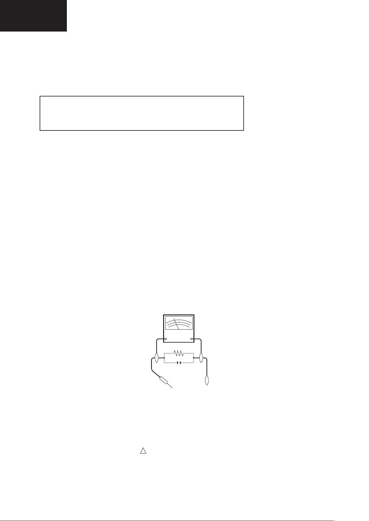
3. To be sure that no shock hazard exists, check for leakage current in the following manner.
IMPORTANT SERVICE SAFETY PRECAUTION
• Plug the AC cord directly into a 220~240 volt AC outlet. (Do not use an isolation transformer for this test).
•Using two clip leads, connect a 1.5k ohm, 10 watt resistor paralleled by a 0.15µF capacitor in series with all exposed metal
cabinet parts and a known earth ground, such as electrical conduit or electrical ground connected to an earth ground.
•A true RMS reading multimeter should be used for this test, especially where the equipment uses a switch mode
power supply which may result in very non-sinusoidal leakage current.
•Connect the resistor connection to all exposed metal parts having a return to the chassis (antenna, metal cabinet,
screw heads, knobs and control shafts, escutcheon, etc.) and measure the AC voltage drop across the resistor.
All checks must be repeated with the AC cord plug connection reversed. (If necessary, a nonpolarized adaptor plug must
be used only for the purpose of completing these checks.)
Any reading of 1.05V peak (this corresponds to 0.7 mA. peak AC.) or more is excessive and indicates a potential shock
hazard which must be corrected before returning the monitor to the owner.
DVM
AC SCALE
1.5k ohm
10W
0.15 µF
TEST PROBE
TO EXPOSED
METAL PARTS
CONNECT TO
KNOWN EARTH
GROUND
SAFETY NOTICE
Many electrical and mechanical parts in LCD television have special safety-related characteristics.
These characteristics are often not evident from visual inspection, nor can protection afforded by them be necessarily
increased by using replacement components rated for higher voltage, wattage, etc.
Replacement parts which have these special safety characteristics are identied in this manual; electrical components
having such features are identied by “ “.
!
For continued protection, replacement parts must be identical to those used in the original circuit.
The use of a substitute replacement parts which do not have the same safety characteristics as the factory recommended
replacement parts shown in this service manual, may create shock, re or other hazards.
8
Page 9
LC-32LE510
L F a
LC-40LE510
PRECAUTIONS FOR USING LEAD-FREE SOLDER
1 Employing lead-free solder
“ALL PWB” of this model employs lead-free solder. The LF symbol indicates lead-free solder, and is attached on the
PWBs and service manuals. The alphabetical character following LF shows the type of lead-free solder.
Example:
Indicates lead-free solder of tin, silver and copper.
L F n
Sn-Ag-Ni
2 Using lead-free wire solder
When xing the PWB soldered with the lead-free solder, apply lead-free wire solder. Repairing with conventional lead
wire solder may cause damage or accident due to cracks.
As the melting point of lead-free solder (Sn-Ag-Cu) is higher than the lead wire solder by 40°C, we recommend you to
use a dedicated soldering bit, if you are not familiar with how to obtain lead-free wire solder or soldering bit, contact our
service station or service branch in your area.
3 Soldering
As the melting point of lead-free solder (Sn-Ag-Cu) is about 220°C which is higher than the conventional lead solder by
40°C, and as it has poor solder wettability, you may be apt to keep the soldering bit in contact with the PWB for extended
period of time. However, Since the land may be peeled off or the maximum heat-resistance temperature of parts may be
exceeded, remove the bit from the PWB as soon as you conrm the steady soldering condition.
Lead-free solder contains more tin, and the end of the soldering bit may be easily corroded. Make sure to turn on and
off the power of the bit as required.
If a different type of solder stays on the tip of the soldering bit, it is alloyed with lead-free solder. Clean the bit after every
use of it.
When the tip of the soldering bit is blackened during use, le it with steel wool or ne sandpaper.
Be careful when replacing parts with polarity indication on the PWB silk.
Lead-free wire solder for servicing.
Indicates lead-free solder of tin, silver and nickel.
9
Page 10
LC-32LE510
A. Information on Disposal for Users (private households)
1. In the European Union
Attention: If you want to dispose of this equipment, please do not use the ordinary dust bin!
Used electrical and electronic equipment must be treated separately and in accordance with legislation that requires
proper treatment, recovery and recycling of used electrical and electronic equipment.
Following the implementation by member states, private households within the EU states may return their used
electrical and electronic equipment to designated collection facilities free of charge*. In some countries* your local
retailer may also take back your old product free of charge if you purchase a similar new one.
*) Please contact your local authority for further details.
If your used electrical or electronic equipment has batteries or accumulators, please dispose of these separately
beforehand according to local requirements.
By disposing of this product correctly you will help ensure that the waste undergoes the necessary treatment, recovery
and recycling and thus prevent potential negative effects on the environment and human health which could otherwise
arise due to inappropriate waste handling.
2. In other Countries outside the EU
If you wish to discard this product, please contact your local authorities and ask for the correct method of disposal.
For Switzerland: Used electrical or electronic equipment can be returned free of charge to the dealer, even if you don’t
purchase a new product. Further collection facilities are listed on the homepage of www.swico.ch or www.sens.ch.
B. Information on Disposal for Business Users
1. In the European Union
If the product is used for business purposes and you want to discard it:
Please contact your SHARP dealer who will inform you about the take-back of the product. You might be charged for
the costs arising from take-back and recycling. Small products (and small amounts) might be taken back by your local
collection facilities.
For Spain: Please contact the established collection system or your local authority for take-back of your used
products.
2. In other Countries outside the EU
If you wish to discard of this product, please contact your local authorities and ask for the correct method of disposal.
Attention: Your product
is marked with this
symbol. It means that
used electrical and
electronic products
should not be mixed
with general household
waste. There is a
separate collection
system for these
products.
End of life disposal
The battery supplied with this product contains traces of Lead.
For EU: The crossed-out wheeled bin implies that used batteries should not be put to the general household waste!
There is a separate collection system for used batteries, to allow proper treatment and recycling in accordance with
legislation. Please contact your local authority for details on the collection and recycling schemes.
For Switzerland: The used battery is to be returned to the selling point.
For other non-EU countries: Please contact your local authority for correct method of disposal of the used battery.
LC-40LE510
END OF LIFE DISPOSAL
10
Page 11
OPERATION MANUAL
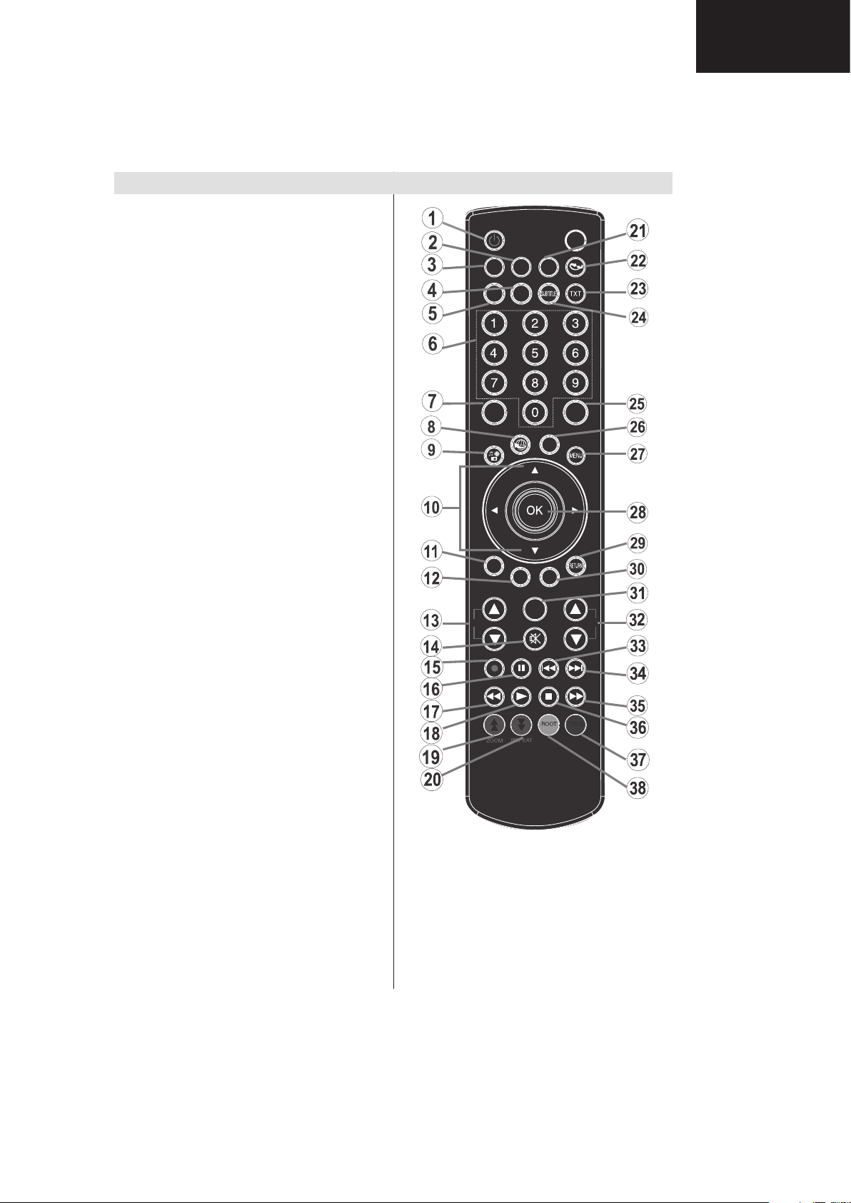
Remote Control Buttons
Standby1.
Image size / Zooms videos (in Media Browser 2.
video mode)
Sleep Timer3.
Mono / Stereo - Dual I-II / Currrent Language (*) 4.
(in DVB channels)
Favourite Mode Selection (in DVB channels)5.
Numeric buttons6.
Electronic programme guide (in DVB channels)7.
No function8.
Media Browser9.
Navigation buttons (Up/Down/Left/Right)10.
No function11.
Recordings Library12.
Programme Down / Page up - Programme Up / 13.
Page down
Mute14.
Programme recording15.
Pause (in Media Browser mode) / Timeshift 16.
recording
Rapid reverse (in Media Browser mode)17.
Play (in Media Browser mode)18.
Red button19.
Green button / List Schedule (in EPG) / Tag 20.
/ Untag All (in favourite list) / Play-Slideshow
(in Media Browser) / Loop-Shuf e (in Media
Browser)
Picture mode selection / Changes picture mode 21.
(in Media Browser video mode)
No function22.
Teletext / Mix (in TXT mode)23.
Subtitle on-off (in DVB channels)24.
Previous programme25.
AV / Source selection26.
Menu on-off27.
Okay (Con rm) / Hold (in TXT mode) / Edit 28.
Channel List
Exit / Return / Index page (in TXT mode)29.
No function30.
Info / Reveal (in TXT mode)31.
Volume Up / Down32.
No function33.
No function34.
Rapid advance (in Media Browser mode)35.
SCREEN
SLEEP
FAV
LANG.
EPG
C
DISP.
CH
Stop (in Media Browser mode)36.
Blue button / Edit Channel List / Filter (In 37.
Favourite List&EPG)
Yellow button / Timeline Schedule (in EPG)38.
INFO
PRESETS
SOURCE
SEARCH
MODE
LC-32LE510
LC-40LE510
SWAP
V
11
Page 12
LC-32LE510
LC-40LE510
Operation Manual (Continued)
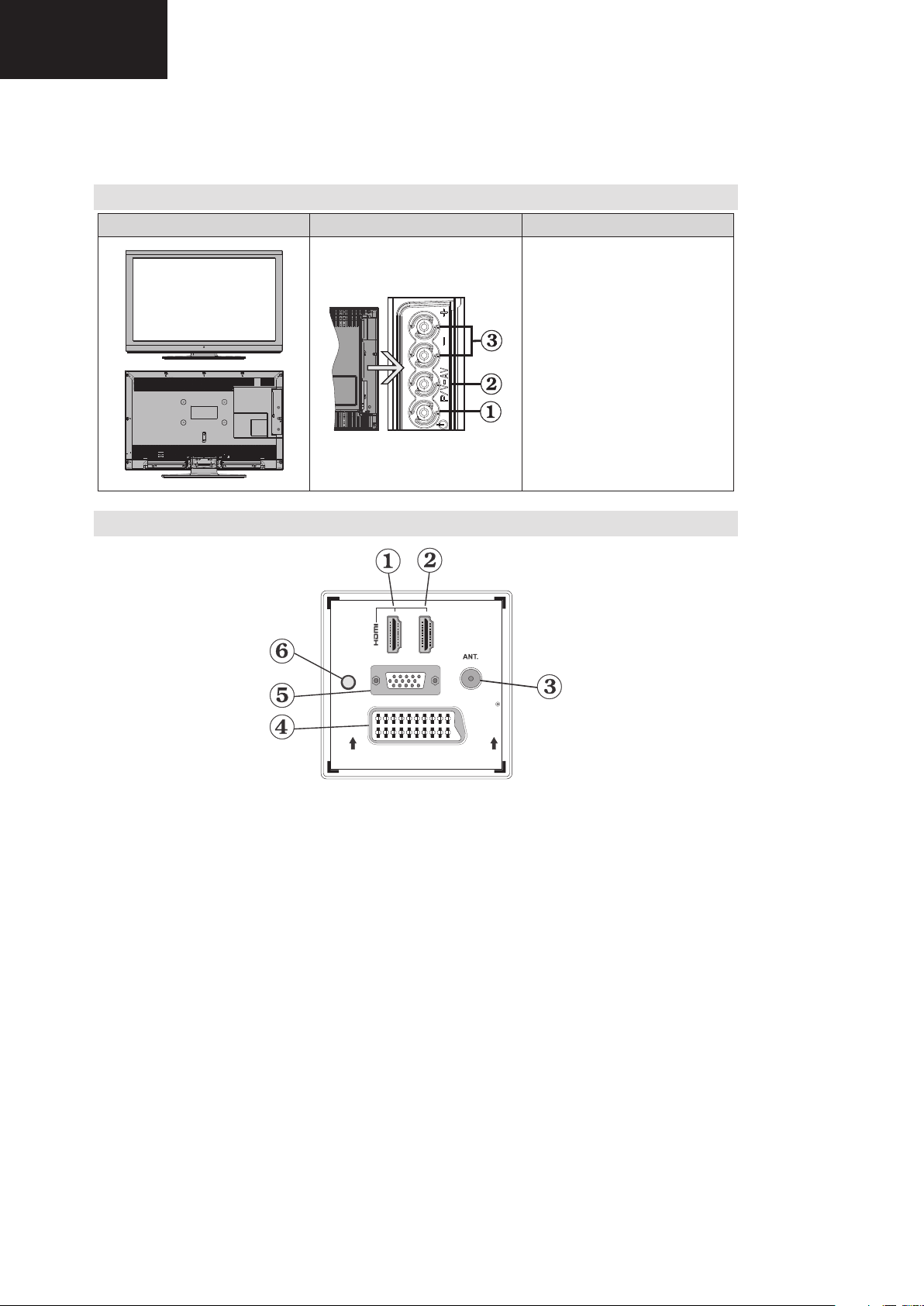
LCD TV and Operating Buttons
FRONT and REAR VIEW Control buttons VIEW Control Buttons
1. Standby Off/On button
2. TV/AV button
3. Programme Up/Down buttons-
Volume Up/Down buttons
Note:You can use +/- buttons
to change volume. If you want
to change channels, press P/V/
AV button once and then use
+/- buttons. If you hold the P/V/
AV button about a few seconds,
source OSD will be displayed.
Main menu OSD cannot be
displayed via control buttons.
Viewing the Connections - Back Connectors
1
2
SPDIF
Coax.OUT
HDMI 2: HDMI Input1.
HDMI 1: HDMI Input2.
HDMI Inputs are for connecting a device that has an HDMI socket. Your LCD TV is capable of
displaying High De nition pictures from devices such as a High De nition Satellite Receiver or DVD
Player. These devices must be connected via the HDMI sockets or Component Socket. These sockets
can accept either 720p or 1080i signals. No sound connection is needed for an HDMI to HDMI
connection.
RF Input3. connects to an aerial antenna system or a cable.
Note that if you use a decoder or a media recorder, you should connect the aerial cable through the device
to the television with an appropriate antenna cable, as shown in the illustration in the following pages.
SCART 4. input or output for external devices. Connect the SCART cable between SCART socket on TV and
SCART socket on your external device (such as a decoder, a VCR or a DVD player).
Note: If an external device is connected via the SCART socket, the TV will automatically switch to AV mode.
Note: S-VHS signal is supported via the scart socket.
PC Input5. is for connecting a personal computer to the TV set.
Connect the PC cable between the PC INPUT on the TV and the PC output on your PC.
SPDIF Coaxial Out6. outputs digital audio signals of the currently watched source.
Use an SPDIF coaxial cable to trasfer audio signals to a device that has SPDIF input
VGA
SCART
12
Page 13
Operation Manual (Continued)
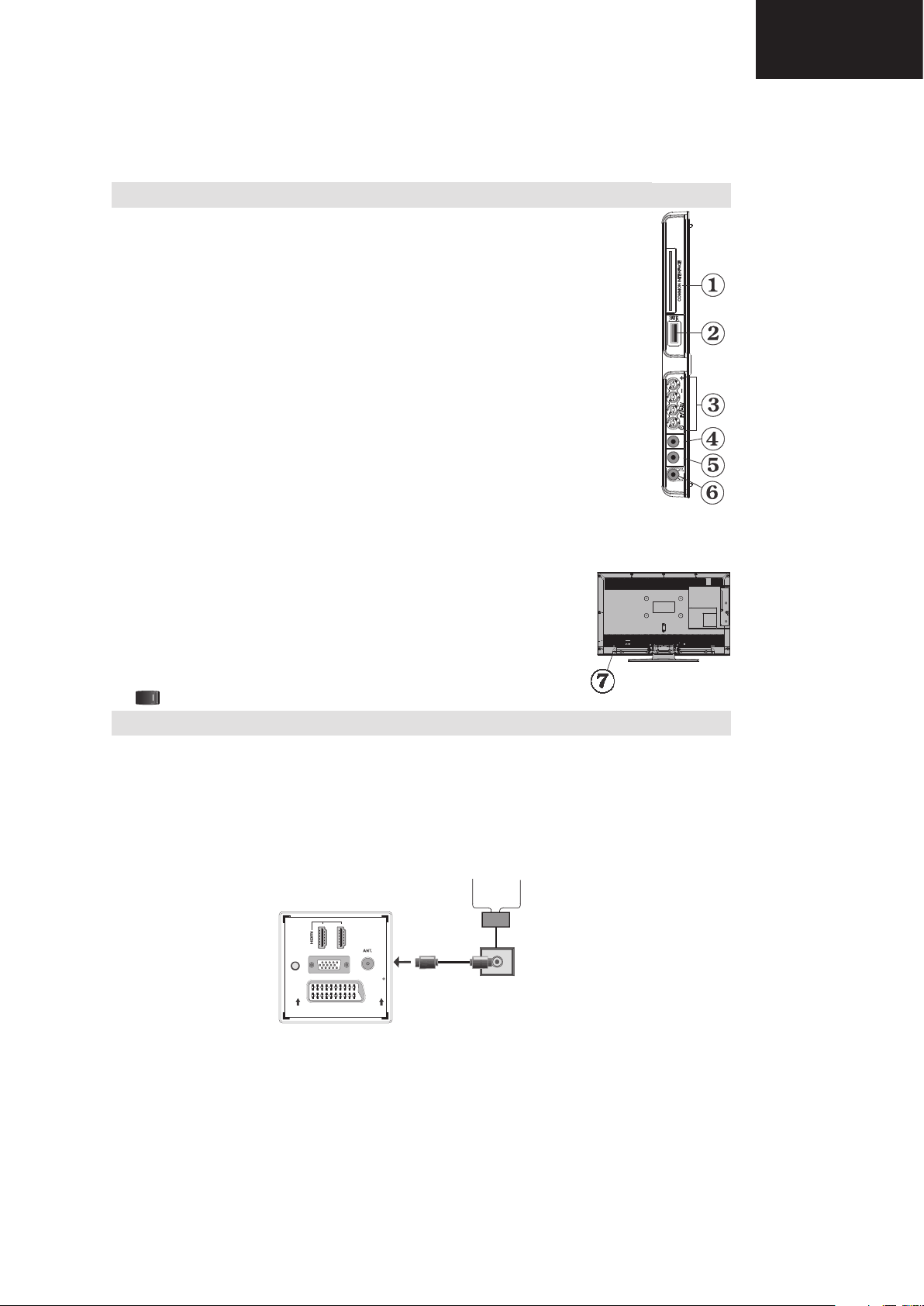
Viewing the Connections - Side Connectors
CI Slot is used for inserting a CI card. A CI card allows you to view all the channels that 1.
you subscribe to. For more information, see “Conditional Access” section.
USB Inputs. 2.
Note that programme recording feature is available via these USB inputs. You can
connect external hard disk drives to this input.
TV control buttons.3.
Component Video Input (YPbPr)4. is used for connecting component video.
You can connect the component video and audio sockets with a device that has
component output. To do this, you must use the supplied component video connection
cable for enabling connection. First, plug single jack of the cable to the TV’s YPbPr
socket (side). Afterwards, insert your component cable’s (not supplied) connectors into
the plural part of the Component video connection cable. Colours of the connected jacks
should match.
Side audio-video connection5. input is used for connecting video and audio signals of
external devices. To make a video connection, you must use the supplied AV connection
cable for enabling connection. First, plug singular jack of the cable to the TV’s Side AV
socket. Afterwards, insert your video cable’s (not supplied) connector into the YELLOW
input (located on the plural side) of the supplied AV connection cable. Colours of the
connected jacks should match.
To enable audio connection, you must use RED and WHITE inputs of the side AV connection cable.
Afterwards, insert your device’s audio cable’s connectors into the RED and WHITE jack of the
supplied side AV connection cable. Colours of the connected jacks should
match.
Note: You should use audio inputs of side AV connection cable (RED &
WHITE) to enable sound connection when connecting a device to your TV by
using PC or COMPONENT VIDEO input.
Headphone jack is used for connecting an external headphone to the 6.
system. Connect to the HEADPHONE jack to listen to the TV from
headphones (optional).
7. , switch is used for turning the TV on or off.
Power Connection
IMPORTANT: The TV set is designed to operate on 220-240V AC, 50Hz.
After unpacking, allow the TV set to reach the ambient room temperature before you connect the set to the •
mains. Plug the power cable to the mains socket outlet.
Aerial Connection
Connect the aerial ,cable TV plug to the AERIAL INPUT socket located at the rear of the TV.•
USB
Max:500mA
LC-32LE510
LC-40LE510
5Vdc
SIDE AV YPbPr
SPDIF
Coax.OUT
Aerial or Cable
1
2
VGA
SCART
13
Page 14

LC-32LE510
LC-40LE510
Operation Manual (Continued)
Using USB Inputs
USB Connection
You can connect a USB hard disk drive or USB •
memory stick to your TV by using the USB inputs
of the TV. This feature allows you to play les stored
in a USB drive or record programmes.
2.5” and 3.5” inch (hdd with external power supply) •
external hard disk drives are supported.
To record a programme, you should rst connect •
a USB disk to your TV while the TV is switched
off. You should then switch on the TV to enable
recording feature. Otherwise, recording feature will
not be available.
IMPORTANT !
You may back up your les before making any •
connections to the TV set in order to avoid any
possible data loss. Note that manufacturer will not
be responsible for any le damage or dataloss.
It is possible that certain types of USB devices (e.g. •
MP3 Players) or USB hard disk drives/memory sticks
may not be compatible with this TV.
IMPORTANT: The TV supports only FAT32 disk
formatting. NTFS format is not supported. If you
connect a USB disk with NTFS format, the TV will ask
you to format the content. See the section, “Format
Disk” in the following pages for more information on
disk formatting.
Note that ALL the data stored on the USB disk will
be lost and then the disk format will be converted to
FAT32 in such a case.
USB Disk Connection
• Plug your USB device to the USB input of the TV.
Note: Plug or unplug your USB disk while the TV is
switched off.
Note: If you are going to connect a USB hard disk drive
to the TV set, USB connection cable used between
the disk drive and the TV should have a USB logo
and should be as short as possible.
Note: While formatting a USB hard disk that has 1TB
(Tera Byte) or more le capacity, you can experience
problems with the formatting process. In such a
case, you should format the disk with your personal
computer and the formatted disk type should be
FAT32.
SIDE VIEW USB MEMORY
USB
5Vdc
Max:500mA
CAUTION !
Quickly plugging and unplugging USB devices, •
is a very hazardous operation. Especially, do not
repeatedly quickly plug and unplug the drive. This
may cause physical damage to the USB player and
especially the USB device itself.
Do not pull out USB module while playing or •
recording a le.
Programme Recording
To record a programme, you should rst connect a
USB disk to your TV while the TV is switched off.
You should then switch on the TV to enable recording
feature.
IMPORTANT: When using a new USB hard disk drive,
it is recommended that you rst format the disk using
your TV’s “Format Disk” option.
To use the recording function a USB 2.0 certi ed •
device of at least 1GB should be used, If the
connected USB device is not USB 2.0 an error
message will be displayed.
Recorded programmes are saved into the connected •
USB disk in .TS format (MPEG-2 transport stream).
If desirable, you can back up / copy these saved
recordings into a personal computer.
Note: It is possible that recorded broadcasts in
.TS format may not be supported by your media
playback software. In such a case, you should install
an appropriate media playback software to your
computer.
An hour of the recordings stored occupies •
approximately 2 GB of space.
For more information on recording programmes, •
see sections “Instant Recording”, “Timeshifting”,
“Electronic Programme Guide”, “Recordings Library”
or “Recording Timers” in the following parts.
Recorded programmes are split into 1GB partitions. •
Names of the stored recordings’ last three digits
indicates this: Such as 4801-000.ts , 4801-001.ts.
Recorded programmes are stored in the following •
directory of the connected USB disk: \DVR\RECS.
All recordings are indicated with a number (such
as 4801-000.ts). A text (txt) le is created for each
recording. This text le includes information such as
broadcaster, programme, and recording time.
If the writing speed of the connected USB disk is not •
suf cient, recording may fail and timeshifting feaute
may not be available.
Recordings of HD programmes can occupy bigger •
size on the USB disk depending on the broadcast’s
resolution. For this reason it is recommended
to use USB hard disk drives for recording HD
programmes.
14
Page 15
Operation Manual (Continued)
LC-32LE510
LC-40LE510
Do not plug out the USB/HDD during the recording. •
This may harm the connected USB/HDD.
Only two partitions on a HDD unit can be •
supported.
Some stream packets may not be recorded because •
of signal problems, so sometimes video may freezes
during playback.
Record, Play, Pause, Display (for PlayListDialog) •
keys could not be used when teletext is ON. If a
recording starts from timer when teletext is ON,
teletext is automatically turned off. Also teletext
usage is disabled when there is ongoing recording
or playback.
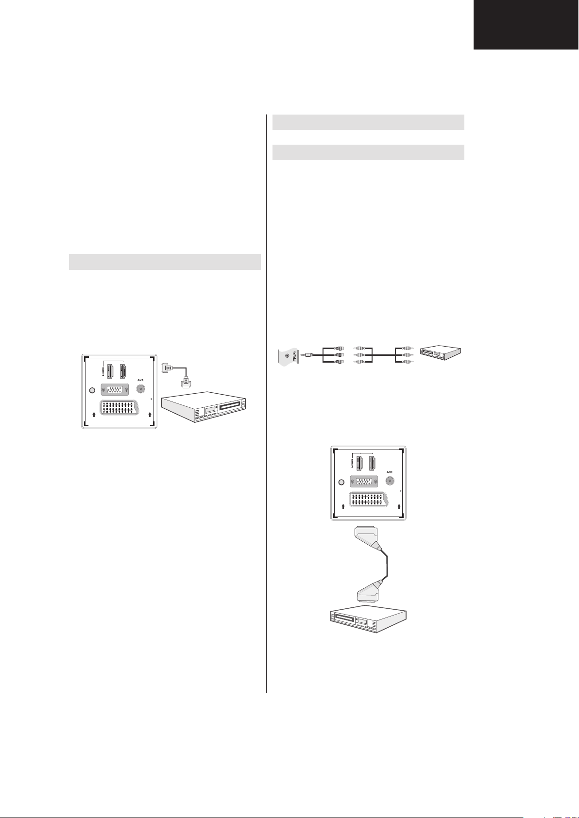
Connecting to a DVD Player via HDMI
Please refer to your DVD player’s instruction book
for additional information. Power off both the TV and
the device before making any connections.
Note: Not all cables shown in the illustration are
supplied.
If your DVD player has an • HDMI socket, you can
connect via HDMI for better video and audio quality.
1
2
VGA
SPDIF
Coax.OUT
SCART
When you connect to DVD player as illustrated above, •
switch to the connected HDMI source. See, Input
Selection section for more information on changing
sources.
HDMI Cable
(not supplied)
External device
Connecting to a DVD Player
via Component Sockets
(YPbPr) or Scart Cable
Some DVD players are connected through •
COMPONENT SOCKETS (YPbPr). In this case,
you must use the supplied Component video
connection cable for enabling connection. First,
plug single jack of the cable to the TV’s YPbPr
socket (side). Afterwards, insert your component
cable’s (not supplied) connectors into the socket
part of the Component video connection cable (see
illustration below). Colours of the connected jacks
should match.
To enable audio connection, use the • VGA/Component
Audio cable. First, plug single jack of the cable
to the TV. Afterwards, insert your DVD player’s
audio cable’s connectors into the socket part of the
VGA/Component audio connection cable (see
illustration below). Colours of the connected jacks
should match.
Side view
YPbPr
Connection Cable
(supplied)
YPbPr Video Cable
(Not supplied)
When the connection is made, switch to •
YPbPr source. See, Input selection section.
Note: To connect YPb Pr device, you should use supplied
component (YPbPr) connection cable
You may also connect through the • SCART input.
1
2
VGA
SPDIF
Coax.OUT
DVD Player
SCART
Scart Cable
(not supplied)
External device
Note• : These three methods of connection perform the
same function but in different levels of quality. It is not
necessary to connect by all three methods.
15
Page 16
LC-32LE510
LC-40LE510
Operation Manual (Continued)
Connecting the LCD TV to a PC
For displaying your computer’s screen image on your
LCD TV, you can connect your computer to the TV set.
Power off both computer and display before making
any connections. Use 15-pin D-sub display cable to
connect a PC to the LCD TV. When the connection
is made, switch to PC source. See “Input selection”
section. Set the resolution that suits your viewing
requirements. Resolution information can be found
in the appendix parts
PC VGA Cable
(Not supplied)
PC Input
(back)
Side AV Input
.
SIDE AV
Side Audio/Video
Connection Cable
(Supplied)
PC Audio Cable
(Not supplied)
Or
Using Side AV Connectors
You can connect a range of optional equipment to your
LCD TV using side connectors of the TV.
For connecting a camcorder or camera , you should •
use AV socket (side). To do this, you must use the
supplied video/audio connection cable. First, plug
single jack of the cable to the TV’s AV IN socket
(side). Afterwards, insert your camera cable’s (not
supplied) connectors into the plural part of the video/
audio connection cable. Colours of the connected
jacks should match. See illustration below.
Afterwards, you should switch to • Side AV source. See
the section Input selection in the following sections
for more information.
AVConnection
Cable (supplied)
SIDE AV
Headphone
To listen the TV sound from headphones, you •
should connect headphones to your TV by using the
HEADPHONE jack as illustrated above..
AV Cable
(not supplied)
Camera
Remote Control Handset
Inserting Batteries
Remove the battery cover located on the back of •
the handset by gently pulling backwards from the
indicated part.
Insert two • AAA/R3 or equivalent type batteries
inside. Observe the correct polarity (+/-) when
inserting batteries and replace the battery cover.
Note: Remove the battery from remote control
handset when it is not to be used for a long period.
Otherwise it can be damaged due to any leakage of
batteries. Remote range is approximately 7m/23ft.
Switching On/Off
To Switch the TV On
Connect the power cord to the 220-240V AC 50 Hz.
Switch the “•
side under the screen to position “|” so the TV will
switch to standby mode. Then the standby LED
lights up.
To switch on the TV from standby mode either:•
Press the “•
button on the remote control.
Press the “•
The TV will then switch on.•
Note : If you switch on your TV via CH
on the remote control or on the TV set, the programme
that you were watching last will be reselected.
By either method the TV will switch on.
To Switch the TV to Standby
To switch the TV to low power stand by press the
” button on the remote control or right hand side
“
of the TV.
Note: When the TV is switched to standby mode,
standby LED can blink to indicate that features such
as Standby Search, Over Air Download or Timer is
active.
To Switch the TV Off
Switch the “• ” button on the bottom right hand
side under the screen to position 2 as illustrated,
” button on the bottom right hand
” button, CH / CH or a numeric
” or +/- button on the TV.
/ CH buttons
to isolate the TV from the mains, the LED will
go out.
16
Page 17
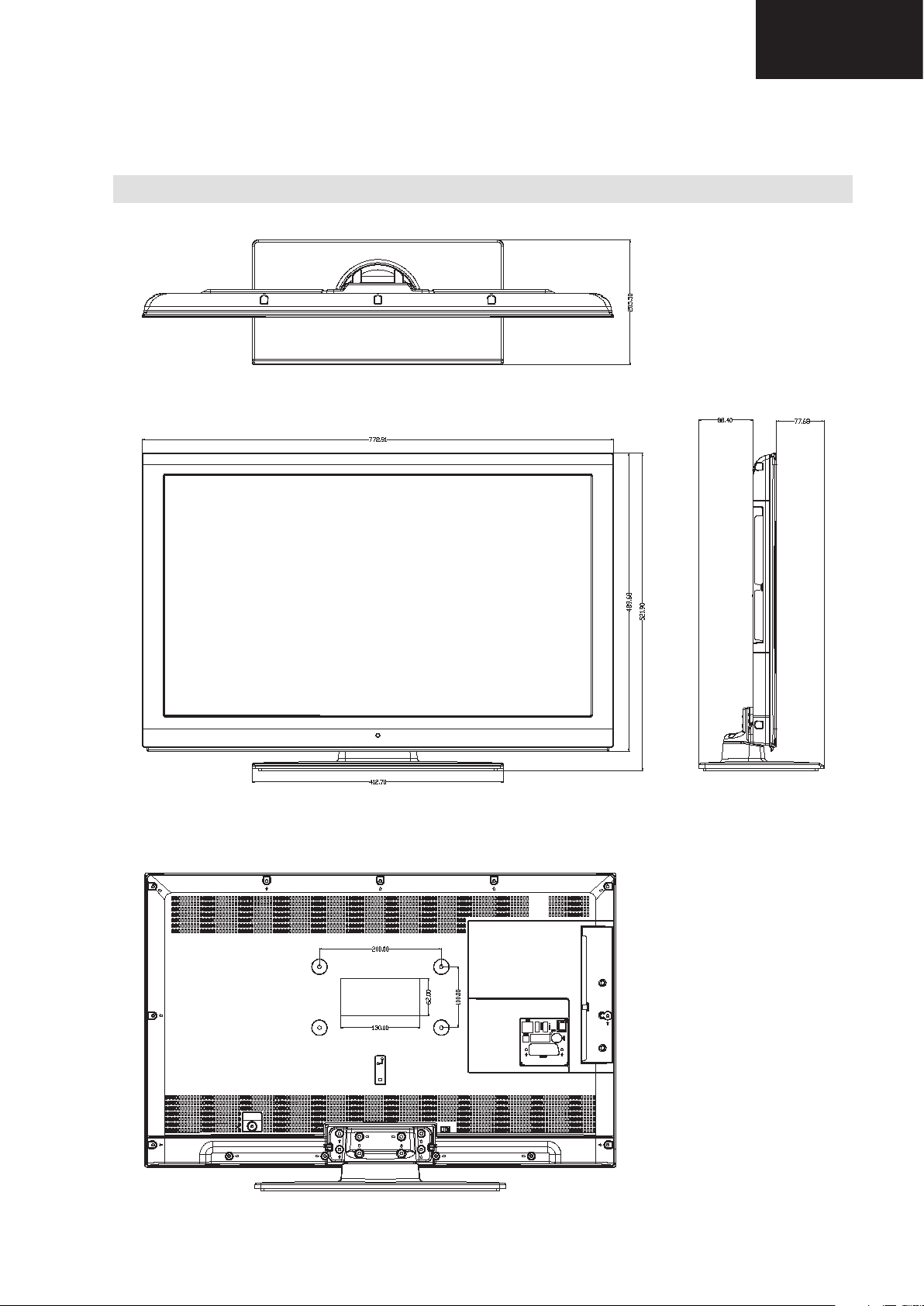
LC-32LE510E Model
Dimensional Drawings
Speci cations
TV BROADCASTING
PAL/SECAM B/G D/K K’ I/I’ L/L’
RECEIVING CHANNELS
VHF (BAND I/III)
UHF (BAND U)
HYPERBAND
NUMBER OF PRESET CHANNELS
1000
CHANNEL INDICATOR
On Screen Display
RF AERIAL INPUT
75 Ohm (unbalanced)
OPERATING VOLTAGE
220-240V AC, 50Hz.
AUDIO
German + Nicam Stereo
AUDIO OUTPUT POWER (W
RMS.
) (10% THD)
2 x 6
POWER CONSUMPTION (W)
135 W (max)
< 0,5 W (Standby)
Digital Reception (DVB-C)
Transmission Standards:
DVB-C, MPEG2, DVB-C, MPEG4
i. DEMODULATION
-Symbolrate: 4.0 Msymbols/s to 7.2 Msymbols/s
- Modulation: 16-QAM , 32-QAM ,64-QAM, 128-QAM
and 256-QAM
ii. VIDEO
- All MPEG2 MP@ML formats with up-conversion and
ltering to CCIR601 format.
-CVBS analogue output
iii. AUDIO
-All MPEG1 Layer 1 and 2 modes
-Sampling frequencies supported are 32, 44.1 & 48
kHz
LC-32LE510
LC-40LE510
DIMENSIONS
PANEL
16:9 display, 32” (80 cm) Screen Size
DIMENSIONS (mm)
DxLxH (With foot): 205,5 x 772,91 x 521,90
Weight (Kg): 10,50
DxLxH (Without foot): 39 x 772,91 x 489,68
Weight (Kg): 9,20
17
Page 18
LC-32LE510
Speci cations
TV BROADCASTING
PAL/SECAM B/G D/K K’ I/I’ L/L’
RECEIVING CHANNELS
VHF (BAND I/III)
UHF (BAND U)
HYPERBAND
NUMBER OF PRESET CHANNELS
1000
CHANNEL INDICATOR
On Screen Display
RF AERIAL INPUT
75 Ohm (unbalanced)
OPERATING VOLTAGE
220-240V AC, 50Hz.
AUDIO
German + Nicam Stereo
AUDIO OUTPUT POWER (W
RMS.
) (10% THD)
2 x 6
POWER CONSUMPTION (W)
190 W (max)
< 0,5 W (Standby)
Digital Reception (DVB-C)
Transmission Standards:
DVB-C, MPEG2, DVB-C, MPEG4
i. DEMODULATION
-Symbolrate: 4.0 Msymbols/s to 7.2 Msymbols/s
- Modulation: 16-QAM , 32-QAM ,64-QAM, 128-QAM
and 256-QAM
ii. VIDEO
- All MPEG2 MP@ML formats with up-conversion and
ltering to CCIR601 format.
-CVBS analogue output
iii. AUDIO
-All MPEG1 Layer 1 and 2 modes
-Sampling frequencies supported are 32, 44.1 & 48
kHz
LC-40LE510
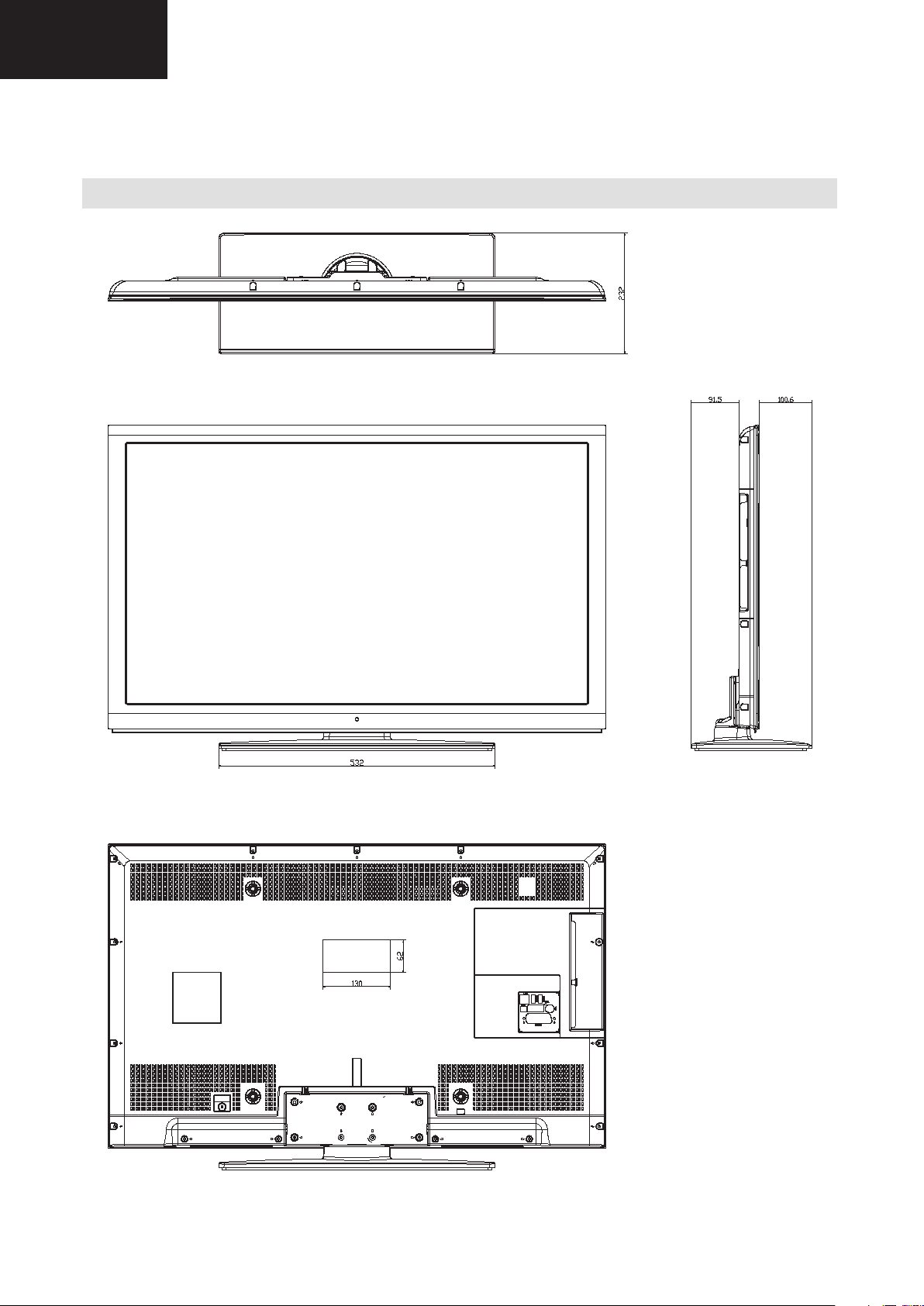
LC-40LE510E Model
Dimensional Drawings
PANEL
16:9 display, 40” Screen Size
DIMENSIONS (mm)
DxLxH (With foot): 232 x 959 x 627
Weight (Kg): 15,20
DxLxH (Without foot): 40 x 959 x 593
Weight (Kg): 12,50
18
Page 19

LC-32LE510
LC-40LE510
INTRODUCTION
1. INTRODUCTION
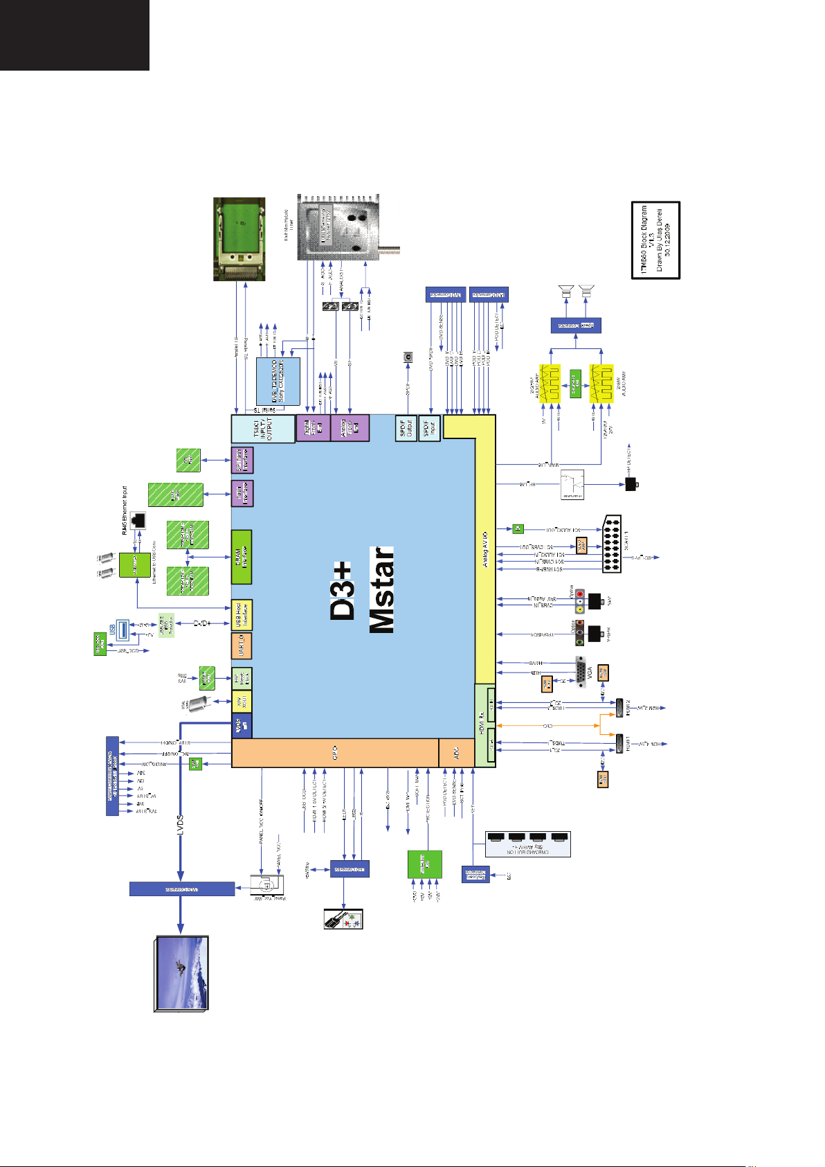
17MB60 mainboard is driven by MStar SOC. This IC is capable of handling Video and audio processing,
Scaling-Display processing, 3D comb filter, OSD and text processing, LVDS transmitting, channel and
MPEG2/4 decoding, integrated DVB-T/C demodulator and media center functionality.
TV supports PAL, SECAM, NTSC color standards and multiple transmission standards as B/G, D/K, I/I’,
and L/L’ including German and NICAM stereo. Also DVB T, DVB-C are supported internal demodulators of
MStar IC and DVB-T2 is supported with external demodulator.
Sound system output is supplying max. 2x2,5W ( less 10%THD at max output) with 4Ω speakers or 2x6W
for stereo 8Ω speakers.
Supported peripherals are:
1 RF input VHF I, VHF III, UHF @ 75Ohm(Common)
1 Side AV (CVBS, R/L_Audio)
1 SCART socket (Common)
1 YPbPr (Optional)
1 PC input (Common)
2 HDMI 1.3 input (1 HDMI input is common, 1 input is optional)
1 S/PDIF output (Optional)
1 Headphone (Optional)
1 Common interface (Common)
1 USB (Common)
1 DVD (Optional)
1 iPod (Optional)
1 On-board Keypad (Optional)
1 External Keypad (Optional)
1 External TouchPad (Optional)
19
Page 20
LC-32LE510
LC-40LE510
1.1 General Block Diagram
20
Page 21
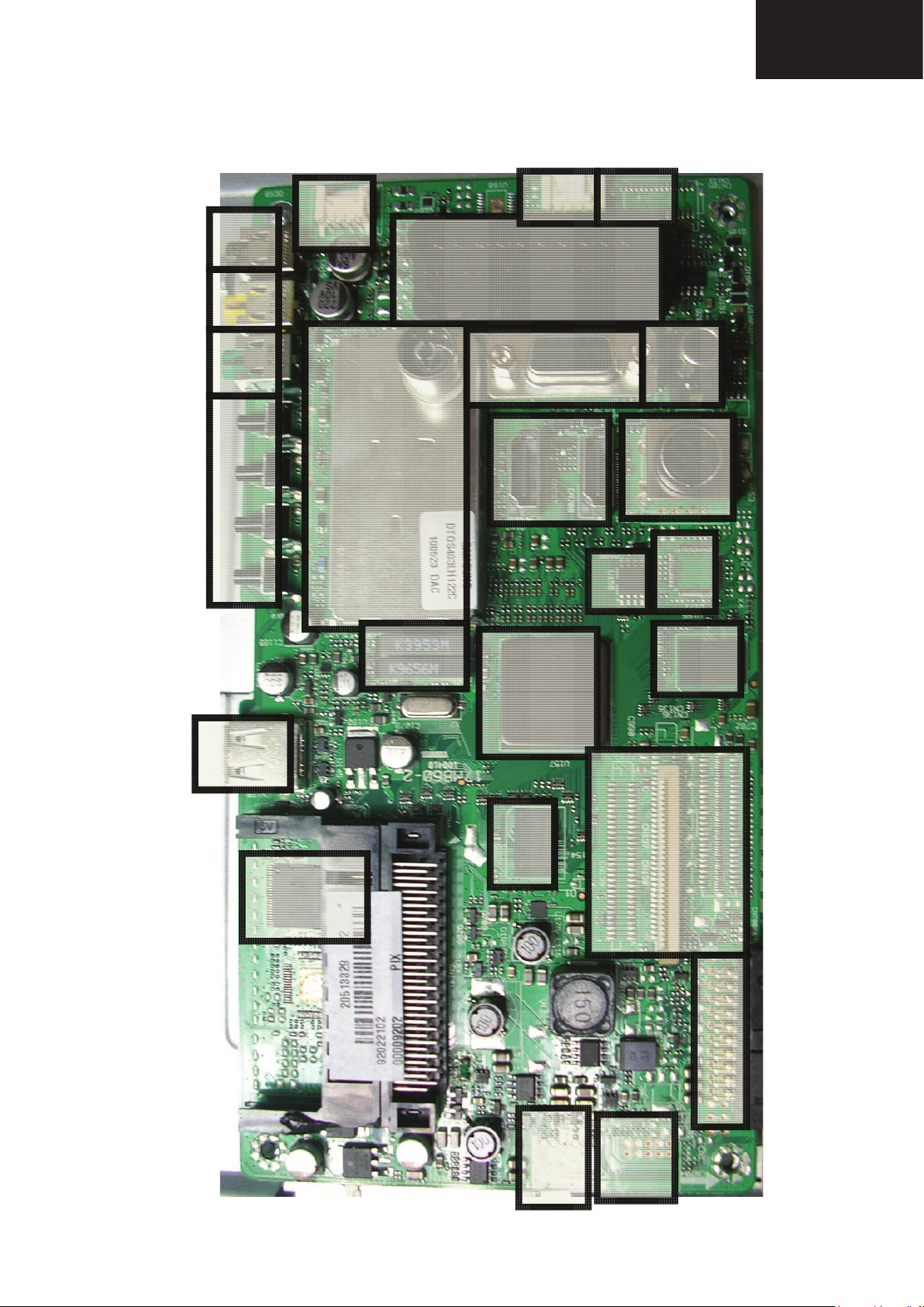
1.2 MB60 Placement of Blocks
(U162)
t IC
DVD
Keyboard
Filter
Keypad
YPbPr
SAV
VGA
SP
DIF
or
Led
Inv.
CI Con
nector
SCART
LC-32LE510
LC-40LE510
Connector
Nand
Flash
Tuner(TU102)
Saw
Main IC (U157)
DDR2
HDMI
SPI
Ethernet
Connector
Etherne
DDR2
LVDS
Connectors
Power Connector
External
21
Page 22
LC-32LE510
LC-40LE510
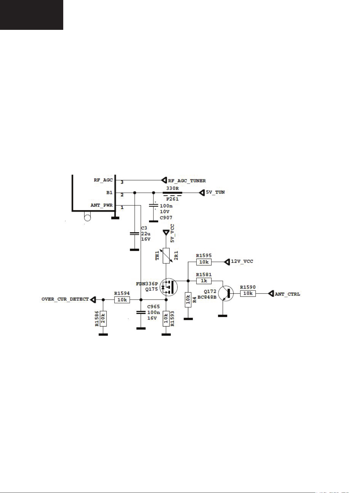
2. TUNER(TU102)
A horizontal mounted and Digital Half-NIM tuner is used in the product, which covers 3 Bands(From 48MHz
to 862MHz for COFDM, from 45.25MHz to 863.25MHz for CCIR CH). The tuning is available through the
digitally controlled I2C bus (PLL). Below you will find info about the tuner.
In active antenna option, the following circuit are used. ANT_CTRL pin is controlled by microcontroller. If
ANT_CTRL is low, ANT_PWR will be low. If ANT_CTRL is high, ANT_PWR will be logic high.
OVER_CUR_DETECT pin is a monitor for short circuit in antenna. OVER_CUR_DETECT is low,
ANT_CTRL will be low, so ANT_PWR will be low. Finally, short circuit protection is done by circuits and
microcontroller.
CIRCUIT DESCRIPTIONS
22
Page 23

LC-32LE510
LC-40LE510
2.1.General description of Samsung DTOS403LH122X:
The Tuner covers 3 Bands(from 48MHz to 862MHz for COFDM, from 45.25MHz to 863.25MHz for CCIR
CH). Band selection and Tuning are performed digitally via the I2C bus.
2.2.Features of DTOS403LH122X:
Receiving System: This TUNER is designed to cover the air channels in VHF and UHF, compliant
with DVB-T standard. and It covers all Analog channels from 48.25MHz to 863.25MHz
Receiving Channel (Digital, Center frequency):
VHF Low CH. E2 ~ S10 ( 50.5MHz ~ 170.5MHz )
VHF High CH. E5 ~ S41 ( 177.5MHz ~ 466 MHz )
UHF CH. E21 ~ E69 ( 474 MHz ~ 858 MHz )
Receiving Channel (PAL, Picture carrier frequency):
VHF Low CH. E2 ~ S10 ( 48.25MHz ~ 168.25MHz )
VHF High CH. E5 ~ S41 ( 175.25MHz ~ 463.25MHz )
UHF CH. E21 ~ E70 ( 471.25MHz ~ 863.25MHz )
Intermediate Frequency:
Digital(center) DVB-T (36.167 MHz)
Digital(center) DVB-C (36.125 MHz)
Analog(picture) 38.9 MHz
Input Impedance : 75Ω, Unbalanced
Band Change-Over System : PLL Control System
Tuning System : Electronic Tuning System With PLL
Internal(or External) RF AGC function :Built in wideband AGC detector with 6 programmable take-
over points
23
Page 24

LC-32LE510
LC-40LE510
Pin no. Terminal Name Pin Description
2.3.Pinning:
1 Ant Power Active Antenna Power
2 B+ +5V, Supply Voltage (Preamplifier, DC/DC)
3 RF AGC RF AGC (internal or external mode)
4 CL I2C Serial Clock
5 DA I2C Serial Clock
6 BP +5V, Supply Voltage (RF Amp, PLL, IF Amp)
7 BT(T.P) +33V, within DC/DC circuit
8 AS I2C Address Selection of the PLL
9 IF AGC Control voltage for the IF AGC
10 IF OUT + Output 2 of the IF Amplifier
11 IF OUT - Output 1 of the IF Amplifier
12 AIF Output IF output of the Analog Broad-Band
24
Page 25
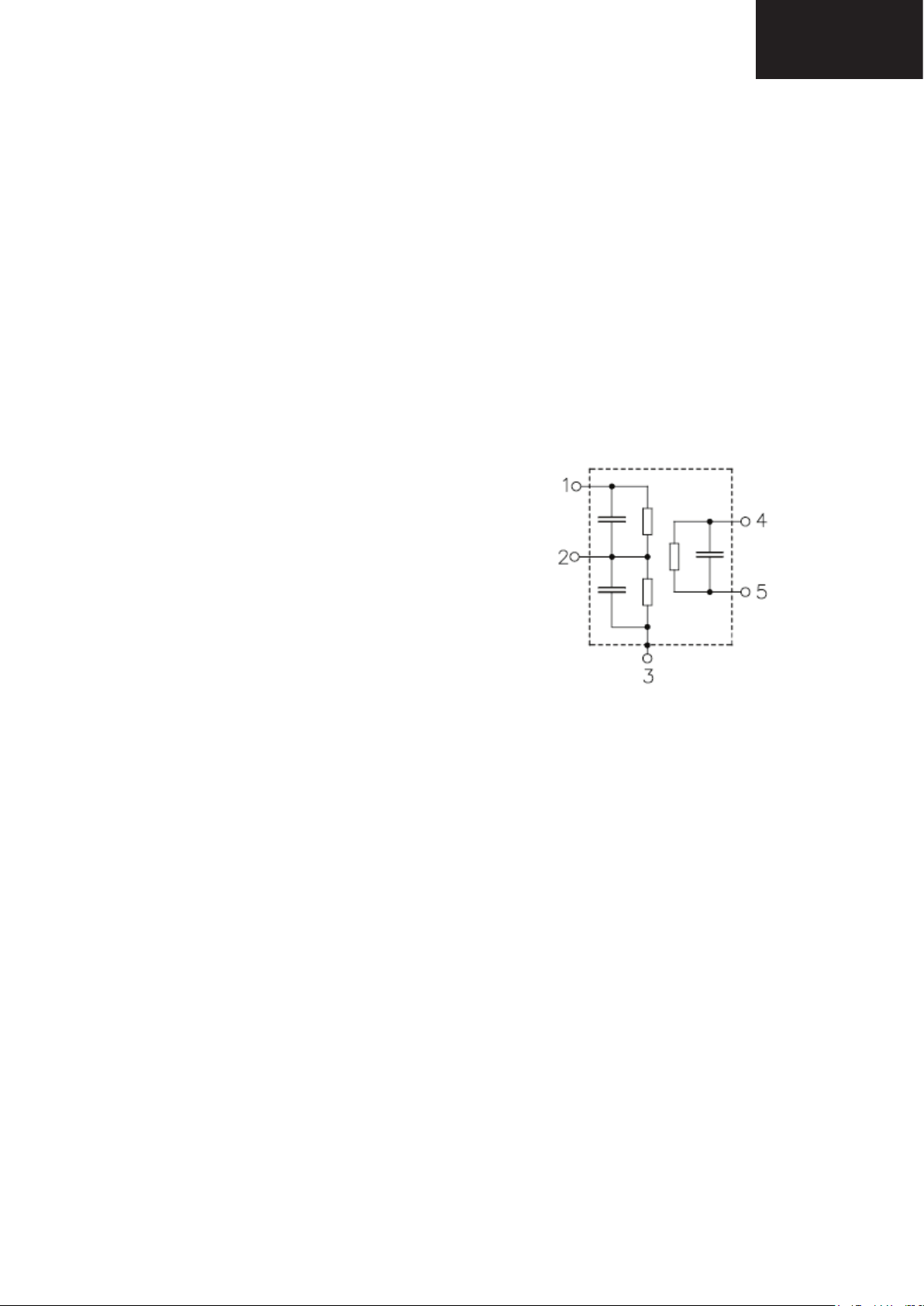
3. SAW FILTER – Audio – Epcos K9656M(Z101)
3.1.Standard
B/G
D/K
I
L/L’
3.2.Features
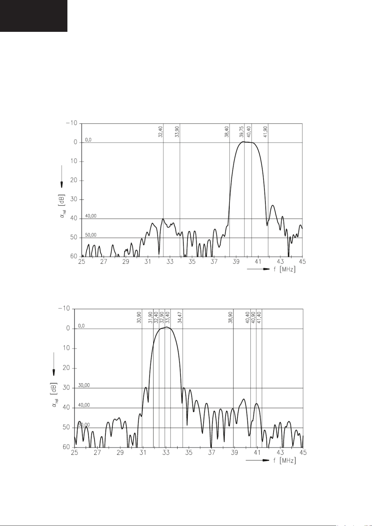
TV IF audio filter with two channels
Channel 1 (L’) with one pass band for sound carriers at 40,40 MHz (L’) and 39,75 MHz (L’-
NICAM)
Channel 2 (B/G,D/K,L,I) with one pass band for sound carriers between 32,35 MHz and
33,40 MHz
LC-32LE510
LC-40LE510
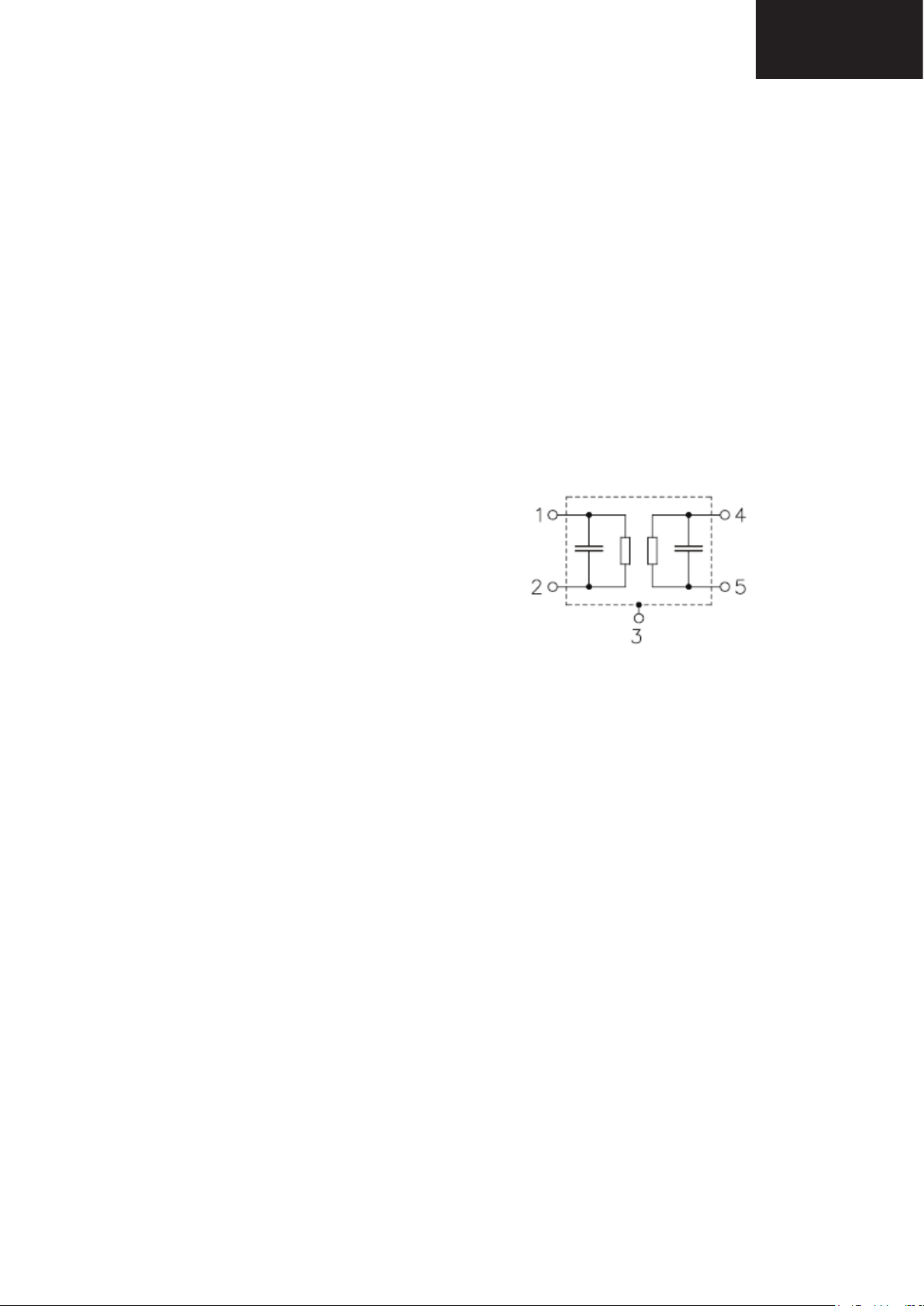
3.3.Pin configuration
1 Input
2 Switching input
3 Chip carrier - ground
4 Output
5 Output
25
Page 26
LC-32LE510
LC-40LE510
3.4.Frequency response
Frequency response of channel 1
Frequency response of channel 2
26
Page 27
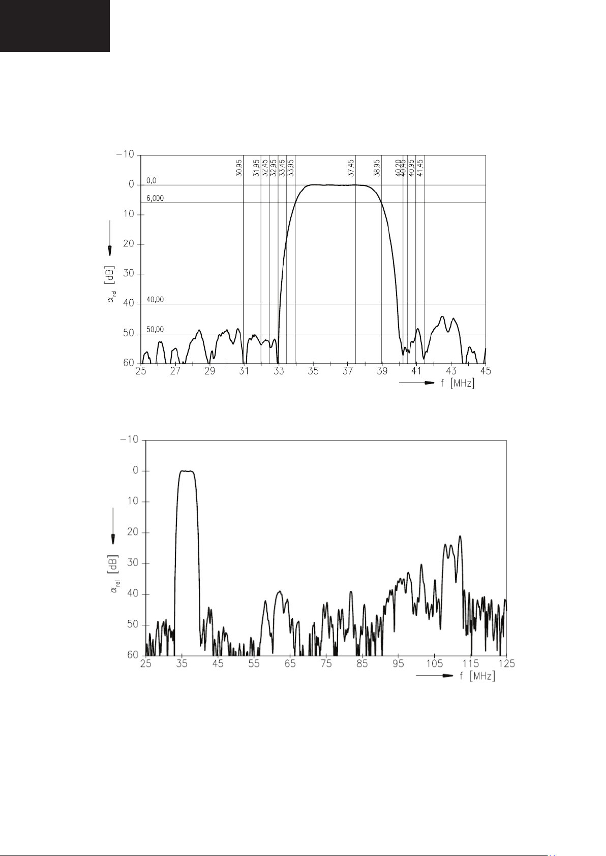
4. SAW FILTER – Video – Epcos K3958M(Z102)
4.1.Standard
B/G
D/K
I
L/L’
4.2.Features
TV IF filter with Nyquist slopes at 33.90 MHz and 38.90 MHz
Constant group delay
4.3.Pin configuration:
LC-32LE510
LC-40LE510
1 Input
2 Input - ground
3 Chip - carrier ground
4 Output
5 Output
27
Page 28
LC-32LE510
LC-40LE510
4.4.Frequency response
28
Page 29

LC-32LE510
LC-40LE510
5. AUDIO AMPLIFIER STAGE WITH AZAD2102(U163, U164)
5.1.General Description
17MB60 uses two 2,5W Class D Mono Audio Amplifers for from 16” to 24” TVs. AZAD2102B is a 2.9 Watts
(max. can offer 3.0 Watts @ Load = 3Ω,THD=10%, AVdd=DVdd=5.5Volt)with high efficiency filter-free
class-D audio power amplifier in a 1613 mm x 1613 mm wafer chip scale package (WCSP). AZAD2102B uses
Current-switch technology to achieve high performance class-d amplifier that features 0.03% THD, 85%
efficiency, –70 dB PSRR, to improve RF-rectification immunity. AZAD2102B provide a Vibration-Spectrum
modulation clock for PWM Output. This vibration frequency is around 10KHZ shift (+/- 5KHZ of Fpwm).
The advantage of the small size package (WCSP) makes AZAD2102B very suitable for mobile phone and
PDA device application. And the Class-D amplifier structure let AZAD2102B to have highly efficiency
power consumption than Class-AB amplifier. AZAD2102B can shrink the application board, reduce system
cost, and external components.
ESD level protection I/O embedded in AZAD2102B. For general applications, doesn’t need to add extra
ESD protection device (like Varistors) in application system for AZAD2102B’s I/O.
5.2.Features
CMOS Technology
High Efficiency 85%
High PSRR 70dB at 217Hz
Differential OP-amp Input
AZAD2102B provides Vibration-Spectrum Modulation clock for reduce EMI
Provide Mute function(set Mute_B to GND will go into Mute status)
For the input stage AZAD2102B built-in a 10Kohm resistors (Gain setting=29.5dB)
Maximum Battery Life and Minimum Heat
Efficiency With an 8-Ω Speaker:
3.5 mA Quiescent Current
Output Power at 10% THD
2.85Watts at AVdd=DVdd=5.0Volt, Rload=4Ω
1.45Watts at AVdd=DVdd=3.6Volt, Rload=4Ω
0.30Watts at AVdd=DVdd=3.0Volt, Rload=4Ω
1.75Watts at AVdd=DVdd=5.5Volt, Rload=8Ω
0.87Watts at AVdd=DVdd=3.6Volt, Rload=8Ω
0.41Watts at AVdd=DVdd=3.0Volt, Rload=8Ω
Eliminate Power on and Power-off “Pop” noise
A Fewer External Components
Optimized PWM Output Stage Eliminates LC Output Filter
Internally generate 290 kHz Switching Frequency to eliminate Capacitor and Resistor
Improve PSRR (–70 dB) and Wide Supply Voltage (3.0 V to 5.5 V)
Fully Differential Design Reduces RF Rectification
This chip has been built-in a very strong ESD protection.
System level ESD 4KV (IEC 61000-4-2 ESD Contact Level)
Wafer Chip Scale Package (WCSP)
TSSOP Package with Exposed Pad
29
Page 30
LC-32LE510
LC-40LE510
5.3.Absolute Ratings
5.3.1.Electrical Characteristics
30
Page 31

5.3.2.Operating Specifications
LC-32LE510
LC-40LE510
31
Page 32

LC-32LE510
LC-40LE510
5.4.Pinning
32
Page 33

LC-32LE510
LC-40LE510
6. AUDIO AMPLIFIER STAGE WITH TPA3113(U168)
6.1.General Description
17MB60 uses a 6W Class D Mono Audio Amplifiers for from 26” to 32” TVs. The TPA3113D2 is a 6-W (per
channel) efficient, Class-D audio power amplifier for driving bridged-tied stereo speakers. Advanced EMI
Suppression Technology enables the use of inexpensive ferrite bead filters at the outputs while meeting
EMC requirements. SpeakerGuard™ speaker protection circuitry includes an adjustable power limiter and
a DC detection circuit. The adjustable power limiter allows the user to set a "virtual" voltage rail lower
than the chip supply to limit the amount of current through the speaker. The DC detect circuit measures
the frequency and amplitude of the PWM signal and shuts off the output stage if the input capacitors are
damaged or shorts exist on the inputs.
The TPA3113D2 can drive stereo speakers as low as 4
eliminates the need for an external heat sink when playing music.
The outputs are also fully protected against shorts to GND, VCC, and output-to-output. The short-circuit
protection and thermal protection includes an auto-recovery feature.
6.2.Features
6-W/ch into an 8-Ω Loads at 10% THD+N From a 10-V Supply
12-W into a 4-Ω Mono Load at 10% THD+N From a 10-V Supply
87% Efficient Class-D Operation Eliminates Need for Heat Sinks
Wide Supply Voltage Range Allows Operation from 8 V to 26 V
Filter-Free Operation
SpeakerGuard™ Speaker Protection Includes Adjustable Power Limiter plus DC Protection
Flow Through Pin Out Facilitates Easy Board Layout
Robust Pin-to-Pin Short Circuit Protection and Thermal Protection with Auto Recovery
Option
Excellent THD+N / Pop-Free Performance
Four Selectable, Fixed Gain Settings
Differential inputs
6.3.Absolute Ratings
Ω. The high efficiency of the TPA3113D2, 87%,
6.3.1.Electrical Characteristics
33
Page 34

LC-32LE510
6.3.Absolute Ratings
6.3.1.Electrical Characteristics
LC-40LE510
6.3.2.Operating Specifications
6.4.Pinning
34
Page 35

LC-32LE510
LC-40LE510
7. POWER STAGE
The DC voltages required at various parts of the chassis and panel are provided by a main power supply
unit. MB60 chassis can operate with IPS60, IPS16, IPS17, PW26, PW27 as main power supply and also with
12V adaptor.
CN706 is used for IPS60, IPS16 and IPS17 and CN1 is used for PW26 and PW27.
JK9 is used for the adapter option and also CN705 inverter socket or DB32 chassis with CN706 is used to
supply backlight.
The power supplies generate 18V, 12V, 5V, 3,3V and 12V, 5V, standby mode DC voltages. Power stage
which is on-chassis generates 5V, 3V3 stand by voltage and 12V, 8V, 5V, 3V3, 2.5V, 1,8V and 1,2V supplies
for other different parts of the chassis. Chassis block diagram is indicated below.
35
Page 36

LC-32LE510
LC-40LE510
̸» ¾´±½µ ±² °±©»® ¾´±½µ ¼·¿¹®¿³ · «·²¹ ¼»°»²¼»²¬ ¬± ³¿·² «°°´§ò Ú±® ĞÉîê ¿²¼
ĞÉîé ¶«¬ ½±³³±² ¾´±½µ ¿®» »²±«¹¸ º±® °®±°»® ±°»®¿¬·±²ò
Ú±® ×ĞÍïêô ×ĞÍïéô ×ĞÍêğ ¾»´±© ¾´±½µ ³«¬ ©±®µ °®±°»®´§ò
36
Page 37

For adopter case also below blocks are necessary.
LC-32LE510
LC-40LE510
7.1. Short CCT Protection Circuit
Short circuit protection is necessary for protecting chassis and main IC against damages when any Vcc
supply shorts to ground. Protect pin should be logic high while normal operation. When there is a short
circuit protect pin should be logic low. After any short detection, SW forces LEDs on LED card to blink.
37
Page 38

LC-32LE510
LC-40LE510
Power Management -- W/Adapter
AC/DC
Adapter
12Vcc1
+1270
12Vcc1
+1408mA
5Vstby
+2682mA
12Vcc1
+460mA
3.3Vstby
+1269mA
Fuse
12Vcc1
@3138mA = 1270mA+1408mA+460mA
P ch
Mosfet
FDC642
DC/DC
MP1583
SO-8
N ch
Mosfet
NTGS3446
DC/DC
MP1484
3A
ADJ SO-8
N ch
Mosfet
NTGS3446
12Vcc2
@1270mA = 1050mA+220mA
5Vstby
@2703mA=21mA+2682
5Vcc
+2682mA
3.3Vstby
@1339mA = 70mA+1269mA
3.3Vcc
+1269mA = 255mA+240mA+774mA
3.3Vcc
+240mA
3.3Vcc
+774mA
Option5 Vcc
+510mA
12Vcc2
220mA
LDO
LM1117
DPAK
DC/DC
MP2012
1.5A
ADJ QFN6
DC/DC
MP1484
3A
ADJ SO-8
2.5V
@ 240mA
1.8V
@ 1135mA
1.26V
@ 1680mA
MB60 Power Management W/PW26
24Vcc @1500mA
Integrated
Power
Supply
PW26
12Vcc2 @2170mA = 1950mA+220mA
5Vcc @1482mA
3.3Vcc @1269mA = 255mA+240mA+774mA
5Vstby @21mA
3.3Vstby @70mA
3.3Vcc
+240mA
3.3Vcc
+774mA
Option5 Vcc
+510mA
12Vcc2
220mA
LDO
LM1117
DPAK
DC/DC
MP2012
1.5A
ADJ QFN6
DC/DC
MP1484
3A
ADJ SO-8
2.5V
@ 240mA
1.8V
@ 1135mA
1.26V
@ 1680mA
38
Page 39

MB60 Power Management W/PW27 & PW03 & PW04
24Vcc 1500mA
Power
Supply
PW27
PW03
PW04
12Vcc2 @2170mA = 1950mA+220mA
5Vcc @1482mA
3.3Vcc @1269mA = 255mA+240mA+774mA
4.2V (Low Power Stby) @91mA = 70mA +21mA
3.3Vcc
+240mA
LM1117
DPAK
DC/DC
LC-32LE510
LC-40LE510
LDO
2.5V
@ 240mA
3.3Vcc
+774mA
LM1117
4.2V 3.3Vstby
4.2Vstby
Or
2x RS1002
JUMPER
JUMPER
@70mA
5Vstby
@21mA
Option5 Vcc
+510mA
12Vcc2
220mA
ADJ QFN6
ADJ SO-8
MB60 Power Management W/IPS16 & IPS17 & IPS60
Integrated
Power
Supply
IPS16
IPS17
IPS60
12Vcc1 @2630mA = 2170mA+460mA
5Vcc @2703mA=21mA+2682mA WO/(510mAOption + Panel Supply)
5Vstby @21mA
3.3Vcc
+240mA
LM1117
MP2012
1.5A
DC/DC
MP1484
3A
LDO
DPAK
1.8V
@ 1135mA
1.26V
@ 1680mA
2.5V
@ 240mA
12Vcc1
+2170mA
12Vcc1
+460mA
3.3Vstby
+1269mA
P ch
Mosfet
FDC642
DC/DC
MP1484
3A
ADJ SO-8
N ch
Mosfet
NTGS3446
12Vcc2
@2170mA = 1950mA+220mA
Option5 Vcc
+510mA
3.3Vstby
@1339mA = 70mA+1269mA
3.3Vcc
+1269mA = 255mA+240mA+774mA
39
3.3Vcc
+774mA
12Vcc2
220mA
DC/DC
MP2012
1.5A
ADJ QFN6
DC/DC
MP1484
3A
ADJ SO-8
1.8V
@ 1135mA
1.26V
@ 1680mA
Page 40

LC-32LE510
The MSD9WB7PX-2 integrates DTV/multi-media all-purpose AV decoder, DVB-T demodulator, VIF
LC-40LE510
8. MICROCONTROLLER – MSTAR(U157)
8.1.General Description
demodulator, and Sound/Video processor into a single device. This allows the overall BOM to be reduced
significantly making the MSD9WB7PX-2 a very competitive multi-media DTV solution. For ATV users, the
MSD9WB7PX-2 provides multi-standard analog TV support with adaptive 3D video decoding and VBI data
extraction. The build-in audio decoder is capable of decoding FM, AM, NICAM, A2, BTSC and EIA-J sound
standards. The MSD9WB7PX-2 supplies all the necessary A/V inputs and outputs to complete a receiver
design including a multi-port HDMI receiver and component video ADC. All input selection multiplexed for
video and audio are integrated, including full SCART support with CVBS output. The equipped MStar
MACE-5 color engine is the latest masterpiece from MStar famous color engine series providing excellent
video and picture quality in Full-HD and large-scale displaying system. To meet the increasingly popular
energy legislative requirements without the use of additional hardware, the MSD9WB7PX-2 has an ultra low
power standby mode during which an embedded MCU can act upon standby events and wake up the
system as required.
8.2.General Features
MSD9WB9PX-2, an SOC solution that supports channel decoding, MPEG decoding, and media-centre
functionality enabled by a high performance AV CODEC and CPU Key features include,
Digital and Analog DVB Front-End Demodulator
A Multi-Standard A/V Format Decoder
The MACE-5 Video Processor
Home Theater Sound Processor
Peripheral and Power Management
Transport Stream De-multiplexer
Supports parallel and serial TS interface, with or without sync signal
Supports TS input and output for external CI module
Maximum TS data rate is 104 Mb/sec for serial or 16 MB/sec for parallel
32 general purpose PID filters and section filters for each transport stream de-multiplexer
Supports additional audio/video/PCR filters
Supports TS DMA channel for time-shift
Supports 3DES/DES and AES encryption/decryption
MPEG-2 Video Decoder
ISO/IEC 13818-2 MPEG-2 video MP@HL
Automatic frame rate conversion
Supports resolution up to HDTV (1080i, 720p) and SDTV
MPEG-4 Video Decoder
ISO/IEC 14496-2 MPEG-4 ASP video decoding
Supports resolutions up to HDTV (1080p@30fps)
Supports DivX1 Home Theater & HD profiles (Optional)
Supports VC-1Optional, FLV video format decoding
40
Page 41

H.264 Decoder
ITU-T H.264, ISO/IEC 14496-10 (main and high profile up to level 4.1) video decoding
Supports resolutions for all DVB, ATSC, HDTV, DVD and VCD
Supports resolution up to 1080p@30fps
Supports CABAC and CAVLC stream types
Processing of ES and PES streams, extraction and provision of time stamps
Up to 40 Mbits bit rate (Bluray spec.)
Hardware JPEG
Supports sequential mode, single scan
Supports both color and grayscale pictures
Following the file header scan the hardware decoder fully handles the decode process
Supports programmable Region of Interest (ROI)
Supports formats: 422/411/420/444/422T
Supports scaling down ratios: 1/2, 1/4, 1/8
Supports picture rotation
LC-32LE510
LC-40LE510
NTSC/PAL/SECAM Video Decoder
Supports NTSC-M, NTSC-J, NTSC-4.43, PAL (B, D, G, H, M, N, I, Nc), and SECAM standards
Automatic standard detection
Motion adaptive 3D comb filter
Five configurable CVBS & Y/C S-video inputs
Supports Teletext, Closed Caption (analog CC 608/ analog CC 708/digital CC 608/digital
CC 708), V-chip and SCTE
Multi-Standard TV Sound Processor
SIF audio decoding
Supports BTSC/A2/EIA-J demodulation
Supports NICAM/FM/AM demodulation
Supports MTS Mode Mono/Stereo/SAP in BTSC/EIA-J mode
Supports Mono/Stereo/Dual in A2/NICAM mode
Built-in audio sampling rate conversion (SRC)
Audio processing for loudspeaker channel, including volume, balance, mute, tone, EQ,
virtual stereo/surround and treble/bass controls
Advanced sound processing options available, for example: Dolby, SRS, BBE, QSound,
Audyssey
Supports digital audio format decoding:
MPEG-1, MPEG-2 (Layer I/II), MP3, Dolby Digital (AC-3), AAC-LC
Supports Optional Dolby Digital Plus, Dolby Pulse, and MS10 multi-stream decoder,
including Dolby Digital Encoder for transcoding streams to Dolby Digital 5.1 (DDCO)
Supports MPEG Audio, Dolby Digital, Dolby Digital Plus format AD (Audio Description)
Supports PVR and time-shifting
Audio Interface
One SIF audio input interface with minimal external saw filters
Four L/R audio line-inputs including Mic. input
41
Page 42

LC-32LE510
LC-40LE510
Analog RGB Compliant Input Port
Two L/R outputs for main speakers and additional line-outputs
Supports stereo headphone driver
I2S digital audio input & output
S/PDIF digital audio output
HDMI audio channel processing
Programmable delay for audio/video synchronization
Three analog ports support up to 1080P
Supports PC RGB input up to SXGA@75Hz
Supports HDTV RGB/YPbPr/YCbCr
Supports Composite Sync and SOG Sync-on-Green
Automatic color calibration
AV-link support
Analogue RGB Auto-Configuration & Detection
Auto input signal format and mode detection
Auto-tuning function including phasing, positioning, offset, gain, and jitter detection
Sync Detection for H/V Sync
DVI/HDCP/HDMI Compliant Input Port
Three HDMI/DVI Input ports
HDMI 1.3 Compliant
HDCP 1.1 Compliant
225MHz @ 1080P 60Hz input with 12-bit Deep-color support
CEC support
Single link DVI 1.0 compliant
Robust receiver with excellent long-cable support
MStar Advanced Color Engine (MStarACE-5)
10/12-bit internal data processing
Fully programmable multi-function scaling engine
Nonlinear video scaling supports various modes including Panorama
Supports dynamic scaling for VC-1
High-Quality DTV video processor
3D motion video deinterlacer with motion object stabilizer
Edge-oriented deinterlacer with edge and artifact smoother
Automatic 3:2/2:2/M:N pull-down detection and recovery
3D multi-purpose noise reduction for DTV or lousy air/cable input
MPEG artifact removal including de-blocking and mosquito noise reduction
Arbitrary frame rate conversion
MStar Professional Picture Enhancement:
o Dynamic brilliant and fresh color
o Dynamic Blue Stretch
o Intensified contrast and details
42
Page 43

Output Interface
ITU J.83 Annex A/C, DVB-C (EN 300 429) compliant
Single/dual link 8/10-bit LVDS output
Supports panel resolution up to Full-HD (1920x1080) @ 60Hz
Supports TH/TI format
Supports dithering options to 6/8-bit output
Spread spectrum output for EMI suppression
LC-32LE510
LC-40LE510
o Dynamic Vivid Skin
o Dynamic sharpened Luma/Chroma edges
o Global and local dynamic depth of field perception
o Accurate and independent color control
o Supports sRGB and xvYCC color processing
o Supports HDMI 1.3 deep color format
o Programmable 12-bit RGB gamma CLUT
CVBS Video Encoder
Supports all NTSC/PAL TV Standard
Stand-alone scaling engine
Programmable Hue, Contract, Brightness
Supports TTX/CC/WSS output
CVBS Video Output
Allows CVBS output of all source inputs
2D Graphics Engine
Hardware Graphics Engine for responsive interactive applications
Supports point draw, line draw, rectangle draw/fill, text draw and trapezoid draw
BitBlt, stretch BitBlt, trapezoid BitBlt, mirror BitBlt and rotate BitBlt
Raster Operation (ROP)
Support Porter-Duff
VIF Demodulator
Compliant with NTSC M/N, PAL B, G/H, I, D/K, SECAM L/L' standards
Audio/Video dual-path processor
Stepped-gain PGA with 25 dB tuning range and 1 dB tuning resolution
Maximum IF gain of 37 dB
Programmable TOP to accommodate different tuner gain and SAW filter insertion loss to
optimize noise and linearity performance
Multi-standard processing with single SAW
Supports silicon tuner low IF output architecture
DVB-T/DVB-C Demodulator
Digital carrier frequency offset correction: ±500KHz
Optimized for SFN channels with pre/post-cursive echoes inside/outside the guard
Acquisition range ±857kHz includes up to 3x: ±1/6 MHz transmitter offset
Meets Nordig Unified 1.0.3, D-Book 5.0, EICTA E-Book/C-Book test requirement
43
Page 44

LC-32LE510
LC-40LE510
Connectivity
Miscellaneous
Supports DVB-C 0.7-7M Baud symbol rate
±400kHz internal carrier offset recovery range
6.8 μsecs echo cancellation at 7 Msym/s
Supports IF, low-IF, zero-IF inputs
Ultra-fast automatic blind UHF/VHF channel scan (constellations and symbol rate)
Two USB 2.0 host ports
USB architecture designed for efficient suppor of external storage devices in conjunction
with off air broadcasting
DRAM interface supporting two 16-bit DDR2 @ 1066MHz
Supports PVR
Supports Common Interface for conditional access support
Bootable SPI interface with serial flash support
Parallel interface for external OneNAND and NAND flash support
Power control module with ultra low power
MCU available in standby mode
523-ball LFBGA package
Operating Voltages: 1.26V (core), 1.8V (DDR2), 2.5V and 3.3V (I/O and analog)
44
Page 45

8.3.MSTAR Block Diagram
LC-32LE510
LC-40LE510
8.4. Reset Circuit
Reset circuit using for initializing main MStar IC. Reset condition is high and normal working condition is low
for RESET pin.
45
Page 46
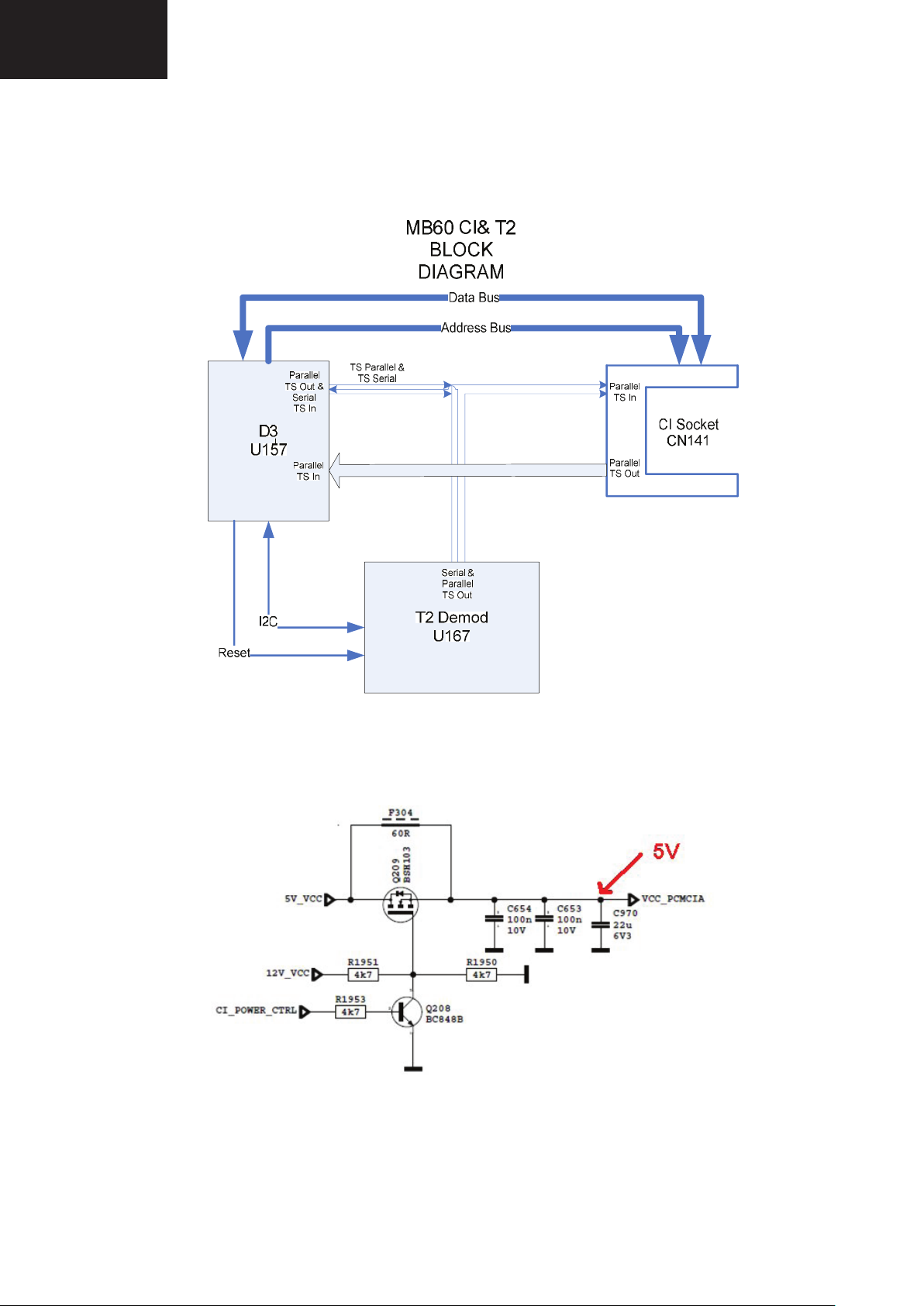
LC-32LE510
LC-40LE510
9. CI INTERFACE
9.1 Block Diagram
9.2 CI Interface Power Switch
It is used for CI module supply, when Module is inserted (it means CI detect is low) This circuit is opened or
closed by CI_POWER_CTRL port of main μController
46
Page 47

LC-32LE510
Integrated USB 2.0 Host interface of D3 (U157)
Protection IC (U145)
Over Current Protection IC (U149)
LC-40LE510
10.
11. USB INTERFACE
Main Concept IC has integrated 2 USB 2.0 interface. One of them is used for Ethernet function, the other
one is used for USB connectivity for last user. Last user can play video, picture and audio files. Also digital
channels can be record to external storage device by this interface. All SW files can be updated with
interface.
USB circuit has 3 main parts
Integrated USB 2.0 Host interface of D3 (U157)
Protection IC (U145)
Over Current Protection IC (U149)
47
Page 48

LC-32LE510
LC-40LE510
12. DDR2 SDRAM 8M × 4 BANKS × 16 BIT (W9751G6JB) (U154, U155)
11.
The W9751G6JB is a 512M bits DDR2 SDRAM, organized as 8,388,608 words × 4 banks × 16 bits. This device
achieves high speed transfer rates up to 1066Mb/sec/pin (DDR2-1066) for general applications.
W9751G6JB is sorted into the following speed grades: -18, -25 and -3. The -18 is compliant to the DDR21066/CL7 specification. The -25 is compliant to the DDR2-800 (5-5-5) or DDR2-800 (6-6-6) specification.
The -3 is compliant to the DDR2-667 (5-5-5) specification. All of the control and address inputs are
synchronized with a pair of externally supplied differential clocks. Inputs are latched at the cross point of
differential clocks (CLK rising and CLK falling). All I/Os are synchronized with a single ended DQS or
differential DQS- DQS pair in a source synchronous fashion.
12.1. General Description
11.1
12.2. Features
11.2
Power Supply: VDD, VDDQ = 1.8 V± 0.1 V
Double Data Rate architecture: two data transfers per clock cycle
CAS Latency: 3, 4, 5, 6 and 7
Burst Length: 4 and 8
Bi-directional, differential data strobes are transmitted / received with data
Edge-aligned with Read data and center-aligned with Write data
DLL aligns DQ and DQS transitions with clock
Differential clock inputs (CLK and CLK )
Data masks (DM) for write data
Commands entered on each positive CLK edge, data and data mask are referenced to both
edges of DQS
Posted CAS programmable additive latency supported to make command and data bus
efficiency
Read Latency = Additive Latency plus CAS Latency (RL = AL + CL)
Off-Chip-Driver impedance adjustment (OCD) and On-Die-Termination (ODT) for better
signal quality
Auto-precharge operation for read and write bursts
Auto Refresh and Self Refresh modes
Precharged Power Down and Active Power Down
Write Data Mask
Write Latency = Read Latency - 1 (WL = RL - 1)
Interface: SSTL_18
11.3
12.3. Electrical Characteristics
48
Page 49

12.4. Pinning
11.4
LC-32LE510
LC-40LE510
49
Page 50

LC-32LE510
LC-40LE510
50
Page 51

12.
13. SCALER AND LVDS SOCKETS
12.1
13.1. LVDS sockets Block Diagram
LC-32LE510
LC-40LE510
12.2
13.2. Panel Supply Switch Circuit
This switch is used to open and close panel supply of TCON. It is controlled by port of main μController.
Also with this circuit panel sequence could be adjusted correctly. 3 panel supplies are connected to this
circuit. All of them are optional according to panels.
51
Page 52

LC-32LE510
LC-40LE510
52
Page 53

LC-32LE510
LC-40LE510
14. NAND FLASH MEMORY - MX25L1005 (U158)
13.
13.1
14.1. General Description
MX25L1005 is a CMOS 1,048,576 bit serial Flash memory, which is configured as 131,072 x 8 internally.
The MX25L1005 feature a serial peripheral interface and software protocol allowing operation on a simple
3-wire bus. The three bus signals are a clock input (SCLK), a serial data input (SI), and a serial data output
(SO). SPI access to the device is enabled by CS# input. The MX25L1005 provide sequential read operation
on whole chip. After program/erase command is issued, auto program/ erase algorithms which program/
erase and verify the specified page or sector/block locations will be executed. Program command is
executed on page (256 bytes) basis, and erase command is executes on chip or sector(4K-bytes) or
block(64K-bytes). To provide user with ease of interface, a status register is included to indicate the status
of the chip. The status read command can be issued to detect completion status of a program or erase
operation via WIP bit. When the device is not in operation and CS# is high, it is put in standby mode and
draws less than 10uA DC current. The MX25L1005 utilize MXIC's proprietary memory cell, which reliably
stores memory contents even after 100,000 program and erase cycles.
13.2
14.2. Features
Serial Peripheral Interface (SPI) compatible -- Mode 0 and Mode 3
1,048,576 x 1 bit structure
32 Equal Sectors with 4K byte each, Any Sector can be erased individually
2 Equal Blocks with 64K byte each, Any Block can be erased individually
Single Power Supply Operation
2.7 to 3.6 volt for read, erase, and program operations
Latch-up protected to 100mA from -1V to Vcc +1V
Low Vcc write inhibit is from 1.5V to 2.5V
13.3
14.3. Absolute Maximum Ratings
RATING VALUE
Ambient Operating Temperature 0°C to 70°C
Storage Temperature -55°C to 125°C
Applied Input Voltage -0.5v to 4.6v
Applied Output Voltage -0.5v to 4.6v
VCC to Ground Potential -0.5v to 4.6v
14.4. Pinning
13.4
8-PIN SOP (150mil)
SYMBOL DESCRIPTION
CS# Chip select
SI Serial Data Input
SO Serial Data Output
SCLK Clock Input
HOLD# Hold, to pause the device without
deselecting the device
VCC +3.3v Power Supply
GND Ground
53
Page 54

LC-32LE510
LC-40LE510
14.
15. NAND FLASH MEMORY – NAND512XXA2C (U162)
15.1. General Description
14.1
The NAND flash 528-byte/ 264-word page is a family of non-volatile flash memories that uses the single
level cell (SLC) NAND technology. It is referred to as the small page family.
The NAND512R3A2C, NAND512R4A2C, and NAND512W3A2C have a density of 512 Mbits and operate with
either a 1.8 V or 3 V voltage supply. The size of a page is either 528 bytes (512 + 16 spare) or 264 words
(256 + 8 spare) depending on whether the device has a x8 or x16 bus width.
The address lines are multiplexed with the Data Input/output signals on a multiplexed x8 or x16
input/output bus. This interface reduces the pin count and makes it possible to migrate to other densities
without changing the footprint.
To extend the lifetime of NAND flash devices it is strongly recommended to implement an error
correction code (ECC). The use of ECC correction allows to achieve up to 100,000 program/erase cycles
for each block. A write protect pin is available to give a hardware protection against program and erase
operations.
14.2
15.2. Features
High density NAND flash memories
512-Mbit memory array
Cost effective solutions for mass storage applications
NAND interface
x8 or x16 bus width
Multiplexed address/ data
Supply voltage: 1.8 V, 3 V
Page size
x8 device: (512 + 16 spare) bytes
x16 device: (256 + 8 spare) words
Block size
x8 device: (16K + 512 spare) bytes
x16 device: (8K + 256 spare) words
Page read/program
Random access: 12 μs (3 V)/15 μs (1.8 V) (max)
Sequential access: 30 ns (3 V)/50 ns (1.8 V) (min)
Page program time: 200 μs (typ)
Copy back program mode
Fast block erase: 2 ms (typ)
Status register
54
Page 55

Electronic signature
Chip Enable ‘don’t care’
Security features
o OTP area
Serial number (unique ID) option
Hardware data protection
o Program/erase locked during power transitions
Data integrity
o 100,000 program/erase cycles (with ECC)
o 10 years data retention
RoHS compliant packages
Development tools
o Error correction code models
o Bad blocks management and wear leveling algorithms
LC-32LE510
LC-40LE510
15.3. Pinning
14.3
55
Page 56

LC-32LE510
LC-40LE510
15.
16. USB2.0 to Fast Ethernet – ASIX AX88X72A (U171)
15.1
16.1. General Description
The AX88772A/AX88172A Low-pin-count USB 2.0 to 10/100M Fast Ethernet controller is a high
performance and highly integrated ASIC which enables low cost, small form factor, and simple plug-andplay Fast Ethernet network connection capability for desktops, notebook PC’s, Ultra-Mobile PC’s, docking
stations, game consoles, digital-home appliances, and any embedded system using a standard USB port.
The AX88772A/AX88172A features a USB interface to communicate with a USB Host Controller and is
compliant with USB specification V1.1 and V2.0. The AX88772A/AX88172A implements 10/100Mbps
Ethernet LAN function based on IEEE802.3, and IEEE802.3u standards with 24KB of embedded SRAM for
packet buffering. The AX88772A/AX88172A integrates an on-chip 10/100Mbps Ethernet PHY to simplify
system design.
The AX88172A provides an optional External Media Interface (EMI) for external PHY or external MAC for
different application purposes. The EMI can be a media-independent interface (MII) for implementing
100BASE-FX Ethernet or HomePNA functions. The EMI can also be a Reverse-MII or Reverse Reduced-MII
(Reverse-RMII) for glueless MAC-to-MAC connections to any MCU with Ethernet MAC MII or RMII interface.
In addition, the EMI can be configured to Dual-PHY mode allowing AX88172A to act as an Ethernet PHY or
USB 2.0 PHY for external MAC device that needs Ethernet and USB interfaces in their system applications.
The optional serial interface such as I2C, SPI, and UART are provided as a control channel from the USB
Host Controller to communicate with the external MCU chip.
15.2
16.2. Features
Single chip USB 2.0 to 10/100M Fast Ethernet controller – AX88772A
USB Device Interface
Integrates on-chip USB 2.0 transceiver and SIE compliant to USB Spec 1.1 and 2.0
Supports USB Full and High Speed modes with Bus-Power or Self-Power capability
Supports 4 or 6 programmable endpoints on USB interface
High performance packet transfer rate over USB bus using proprietary burst transfer
mechanism
Supports USB to Ethernet bridging or vice versa in hardware
Fast Ethernet Controller
Integrates 10/100Mbps Fast Ethernet MAC/PHY
IEEE 802.3 10BASE-T/100BASE-TX compatible
Supports twisted pair crossover detection and auto-correction (HP Auto-MDIX)
Embedded 16KB SRAM for RX packet buffering and 8KB SRAM for TX packet buffering
Supports both Full-duplex with flow control and
Half-duplex with backpressure operation
Supports 2 VLAN ID filtering, received VLAN Tag (4 bytes) can be stripped off or preserved
MAC/PHY loop-back diagnostic capability
Support Wake-on-LAN Function
56
Page 57

Supports Suspend Mode and Remote Wakeup via Link-up, Magic packet, MS wakeup frame
and external pin
Optional PHY power down during Suspend Mode
Versatile External Media Interface
Optional MII interface in MAC mode allows AX88172A to work with external 100BASE-FX
Ethernet PHY or HomePNA PHY
Optional Reverse-MII or Reverse-RMII interface in PHY mode allows AX88172A to work with
external HomePlug PHY or glueless MAC-to-MAC connections
Optional Reverse-MII interface in Dual-PHY mode allows AX88172A to act as an Ethernet
PHY or USB 2.0 PHY for external MAC device that needs Ethernet and USB in system
application
Supports 256/512 bytes (93c56/93c66) of serial EEPROM (for storing USB Descriptors)
Supports automatic loading of Ethernet ID, USB Descriptors and Adapter Configuration
from EEPROM after power-on initialization
Provides optional serial interface, I2C, SPI and UART
Integrates on-chip voltage regulator and only requires a single 3.3V power supply
12MHz and 25Mhz clock input from either crystal or oscillator source
Integrates on-chip power-on reset circuit
LC-32LE510
LC-40LE510
16.3. Block Diagram
15.3
15.4
16.4. Pinning
57
Page 58

LC-32LE510
16.4. Pinning
LC-40LE510
17. LM1117(U175, U180, U181)
16.
17.1. General Description
16.1
The LM1117 is a series of low dropout voltage regulators with a dropout of 1.2V at 800mA of load current. It
has the same pin-out as National Semiconductor’s industry standard LM317. The LM1117 is available in an
adjustable version, which can set the output voltage from 1.25V to 13.8V with only two external resistors. In
addition, it is also available in five fixed voltages, 1.8V, 2.5V, 2.85V, 3.3V, and 5V. The LM1117 offers
current limiting and thermal shutdown. Its circuit includes a zener trimmed band-gap
reference to as-sure output voltage accuracy to within ±1%. The LM1117 series is available in SOT- 223,
TO-220, and TO-252 D-PAK packages. A minimum of 10μF tantalum capacitor is required at the output to
improve the transient response and stability.
17.2. Features
16.2
16.3
17.3. Applications
Available in 1.8V, 2.5V, 2.85V, 3.3V, 5V, and Adjustable Versions
Space Saving SOT-223 Package
Current Limiting and Thermal Protection
Output Current 800mA
Line Regulation 0.2% (Max)
Load Regulation 0.4% (Max)
Temperature Range
LM1117 0°C to 125°C
LM1117I -40°C to 125°C
2.85V Model for SCSI-2 Active Termination
Post Regulator for Switching DC/DC Converter
High Efficiency Linear Regulators 15
32” TFT TV Service Manual 10/01/2005
Battery Charger
Battery Powered Instrumentation
16.4
17.4. Absolute Maximum Ratings
17.5. Pinning
16.5
58
Page 59

LC-32LE510
LC-40LE510
17.
18. MP2012 (U176)
18.1. General Description
17.1
The MP2012 is a fully integrated, internally compensated 1.2MHz fixed frequency PWM step-down
converter. It is ideal for powering portable equipment that runs from a single cell Lithium-Ion (Li+) Battery,
with an input range from 2.7V to 6V. The MP2012 can provide up to 1.5A of load current with output voltage
as low as 0.8V. It can also operate at 100% duty cycle for low dropout applications. With peak current mode
control and internal compensation, the MP2012 is stable with ceramic capacitors and small inductors. Fault
condition protection includes cycle-by-cycle current limiting and thermal shutdown.
17.2
18.2. Features
2.7-6V Input Operation Range
Output Adjustable from 0.8V to VIN
1μA Max Shutdown Current.
Up to 95% Efficiency
100% Duty Cycle for Low Dropout
Applications
1.2MHz Fixed Switching Frequency
Stable with Low ESR Output Ceramic
Capacitors
Thermal Shutdown
Cycle-by-Cycle Over Current Protection
Short Circuit Protection
Available in 6-pin 3x3mm QFN
18.3. Pinning
17.3
Pin
#
1 FB Feedback input. An external resistor divider from the output
2 GND, Exposed
3 SW Switch node to the inductor.
4 PVIN Input supply pin for power FET.
5 VIN Input Supply pin for controller. Put small decoupling
6 EN Enable input, “High” enables MP2012. EN is pulled to GND
Name Description
to GND, tapped to the FB pin sets the output voltage.
Ground pin. Connect exposed pad to ground plane for
Pad
proper thermal performance.
ceramic near this pin.
with 1Meg internal resistor.
59
Page 60

LC-32LE510
LC-40LE510
18.
19. RTA8283A (U23, U173)
The RT8283A is a high-efficiency, monolithic synchronous step-down DC/DC converter that can deliver up
to 3A output current from a 4.5V to 23V input supply. The RT8283A's current mode architecture and
external compensation allow the transient response to be optimized over a wide range of loads and output
capacitors. Cycle-by-cycle current limit provides protection against shorted outputs and soft-start eliminates
input current surge during start-up. The RT8283A also provides output under voltage protection and thermal
shutdown protection. The low current (<3μA) shutdown mode provides output disconnect, enabling easy
power management in battery powered systems. The RT8283A is available in a SOP-8 package.
19.1. General Description
18.1
18.2
19.2. Features
±1.5% High Accuracy Feedback Voltage
Integrated N-MOSFET Switches
Current Mode Control
Fixed Frequency Operation : 340kHz
Output Adjustable from 0.8V to 20V
Up to 95% Efficiency
Thermal Shutdown Protection
60
Page 61

18.3
19.3. Pinning
LC-32LE510
LC-40LE510
Pin No. Pin
1
2
3
4, 9 (Exposed
Pad)
5
6
Description
Name
BOOT
VIN Input Supply 4.5V to 23V. Must bypass with a suitably
SW Phase Node--Connect to external L-C filter..
GND Ground.
FB Feedback Input pin is connected to the converter output.
COMP Compensation Node. COMP is used to compensate the
Bootstrap for high-side gate driver. Connect a 0.1μF or
greater ceramic capacitor from BOOT to SW pins.
large ceramic capacitor.
It is used to set the output of the converter to regulate to
the desired value via an internal res divider. For an
adjustable output, an external res divider is connected to
this pin.
regulation Control loop. Connect a series RC network
from COMP to GND. In some cases, an additional
capacitor from COMP to GND is required.
7
8
EN Enable Input Pin. Logic high enables the converter; a
logic low forces the RT8253A into shutdown mode.
Attach this pin to VIN with a 100kΩ pull up resistor for
automatic startup.
SS Soft-Start Control Input. SS controls the soft-start period.
Connect a capacitor from SS to GND to set the soft-start
period. A 0.1μF capacitor sets the soft-start period to
13.5ms.
61
Page 62

LC-32LE510
threshold is 1.222V.
20. MP1583 (U174)
20.1. General Description
The MP1583 is a step-down regulator with a built-in internal Power MOSFET. It achieves 3A of continuous
output current over a wide input supply range with excellent load and line regulation. Current mode
operation provides fast transient response and eases loop stabilization. Fault condition protection
includes cycle-by-cycle current limiting and thermal shutdown. An adjustable soft-start reduces the
stress on the input source at start-up. The MP1583 requires a minimum number of external components,
providing a compact solution.
20.2. Features
3A Output Current
Programmable Soft-Start
100mΩ Internal Power MOSFET Switch
Stable with Low ESR Output Ceramic Capacitors
Up to 95% Efficiency
20μA Shutdown Mode
Fixed 385KHz Frequency
Thermal Shutdown
Cycle-by-Cycle Over Current Protection
Wide 4.75V to 23V Operating Input Range
Output Adjustable from 1.22V to 21V
Under-Voltage Lockout
20.3. Pinning
LC-40LE510
20. MP1583 (U174)
19.
20.1. General Description
19.1
The MP1583 is a step-down regulator with a built-in internal Power MOSFET. It achieves 3A of continuous
output current over a wide input supply range with excellent load and line regulation. Current mode
operation provides fast transient response and eases loop stabilization. Fault condition protection
includes cycle-by-cycle current limiting and thermal shutdown. An adjustable soft-start reduces the
stress on the input source at start-up. The MP1583 requires a minimum number of external components,
providing a compact solution.
19.2
20.2. Features
3A Output Current
Programmable Soft-Start
19.3
20.3. Pinning
100mΩ Internal Power MOSFET Switch
Stable with Low ESR Output Ceramic Capacitors
Up to 95% Efficiency
20μA Shutdown Mode
Fixed 385KHz Frequency
Thermal Shutdown
Cycle-by-Cycle Over Current Protection
Wide 4.75V to 23V Operating Input Range
Output Adjustable from 1.22V to 21V
Under-Voltage Lockout
Pin
No.
1
2
3
Pin
Name
BOOT High-Side Gate Drive Bootstrap Input. BS supplies the drive for the
IN Power Input. Drive IN with a 4.75V to 23V power source.
SW Power Switching Out is the switching node that supplies power to the
Description
high-side N-Channel MOSFET switch.
output
4
5
6
7
8
GND Ground.
FB Feedback Input. FB senses the output voltage and regulates it. Drive
FB with a resistive voltage divider from the output voltage. FB
COMP Compensation Node is used to compensate the regulation control
loop.
EN Enable/UVLO. A voltage greater than 2.71V enables operation. For
complete low current shutdown the EN pin voltage needs to be at less
than 900mV. When the voltage on EN exceeds 1.2V, the internal
regulator will be enabled and the soft-start capacitor will begin to
charge. The MP1583 will start switching after the EN pin voltage
reaches 2.71V.
SS Soft-Start Control Input. SS controls the soft-start period.
62
Page 63

LC-32LE510
process that
LC-40LE510
20.
21. FDC642
20.1
21.1. General Description
This P-Channel 2.5V specified MOSFET is produced using Fairchild’s advanced PowerTrench®
has been especially tailored to minimize on-state resistance and yet maintain low gate charge for
superior switching performance.
These devices have been designed to offer exceptional power dissipation in a very small footprint for
applications where the larger packages are impractical.
20.2
21.2. Features
Max rDS(on) = 65 mΩ at VGS = -4.5 V, ID = -4.0 A
Max rDS(on) = 100 mΩ at VGS = -2.5 V, ID = -3.2 A
Fast switching speed
Low gate charge (11nC typical)
High performance trench technology for extremely low rDS(on)
SuperSOTTM-6 package: small footprint (72% smaller than standard SO-8); low profile (1
mm thick)
Termination is Lead-free and RoHS Compliant
20.3
21.3. Pinning
63
Page 64

LC-32LE510
LC-40LE510
21.
22. FDC604P
This P-Channel 1.8V specified MOSFET uses Fairchild’s low voltage PowerTrench process. It has been
optimized for battery power management applications.
21.1
22.1. General Description
21.2
22.2. Features
–5.5 A, –20 V. RDS(ON) = 33 mΩ @ VGS = –4.5 V
RDS(ON) = 43 mΩ @ VGS = –2.5 V
RDS(ON) = 60 mΩ @ VGS = –1.8 V
Fast switching speed.
High performance trench technology for extremely low RDS(ON)(S)
21.3
22.3. Pinning
64
Page 65

23. CONNECTORS
22.
23.1. SCART (SC1)
22.1
LC-32LE510
LC-40LE510
22.2
23.2. HDMI (CN 707,CN708)
65
Page 66

LC-32LE510
LC-40LE510
22.3
23.3. VGA (CN1 32)
66
Page 67

SERVICE MENU SETTINGS
23.
24. SERVICE MENU SETTINGS
In order to reach service menu, First Press “MENU” Then press the remote control code two times,
which is “4725”.
In first screen following items can be seen:
LC-32LE510
LC-40LE510
67
Page 68

LC-32LE510
24.1. Video Settings
LC-40LE510
23.1 Video Settings
23.2 Audio Settings
68
Page 69

23.3 Options
Options
Options-1
LC-32LE510
LC-40LE510
69
Page 70

LC-32LE510
24.3. Tuning Settings
24.4. Source Settings
LC-40LE510
23.4 Tuning Settings
23.5 Source Settings
70
Page 71

24.5. Diagnostic
23.6 Diagnostic
24.6. USB Operations
LC-32LE510
LC-40LE510
23.7 USB Operations
USB operations option cannot be used directly. It can be used for updating panel tool, hw configuration
etc.
71
Page 72

LC-32LE510
24.6. USB Operations
USB operations option cannot be used directly. It can be used for updating panel tool, hw configuration
etc.
LC-40LE510
24.
25. SOFTWARE UPDATE
SOFTWARE UPDATE
Analog - Digital SW update via USB
1. Please copy the files to USB (root).
• mb60_en.bin
• mboot.bin
• usb_auto_update.txt
2. Turn power to OFF by mechanical switch(rocker switch) or removing AC
plug. And plug the USB to TV
3. Keep pressing OK key from remote controller and then turn the TV power
to ON(by mechanical switch or by inserting the AC plug) and keep OK key
pressed until the stanby led blinks rapidly(rapid blinking is faster than
normal blinking)
4. When the led is started to blink rapidly, you can release the OK key.Please
wait approximately for 1-2 minutes.
5. When the blinks of led is stopped, TV opens autamatically with the new
SW.
72
Page 73

25. HOTEL TV MODE
DTG D-book 6.2 (HD MHEG5 compliant)
MHEG5 v1.06 compliant
MPEG2 MP@ML support (main profile main level)
MPEG4 HP@HL support (high profile high level) (MPEG4 models only)
H264 AVC SD-HD support (MPEG4 models only)
Multi language audio support
Multi language subtitle support
Audio Description
2.14 Hotel TV mode
LC-32LE510
LC-40LE510
HOTEL TV MODE
25.1 HOTEL TV FEATURES:
The HOTEL TV is a special mode which restricts some operations of TV. This allows the customer to use the TV
in hotels or in Hospitals. The restrictions of a hotel TV are basically given below.
1. The user cannot increase the volume above a specified limit. And could set fixed volume.
2. The user could enable headphone direct volume control.
3. The user cannot reach some menus.
4. The user cannot use panel.
5. Start up source position can be limited for the user.
6. Last status could be used or not
7. Teletext could be disabled or enabled.
8. NVRAM data (like service list and user preferences, etc.) could be copied or set via USB device
9. Pin8 could be used or not
25.2 HOTEL TV MENU:
To enter hotel menu, please open main menu by pressing MENU(M) button. When you code following password
“7935”, hidden hotel TV menu appears.
25.3 Hotel Mode
Setting “Hotel Mode” item 'On' activates hotel mode. In other words user can do only what he/she is allowed to
do. Restriction level can be determined by using other items on menu namely Volume Limit, Panel Button, OSD
Disable. In hotel mode, users can not reach channel table and install menu so they could not change any
program information.
25.4 Last Status
Setting “Last Status” item to 'On' enable TV open with the closing status. Otherwise, if “Last
Status” item is set 'Off' TV opens with standby status.
25.5 Panel Lock
Enables (Panel Lock = On) or prohibits (Panel Lock = Off) the use of front panel buttons.
25.6 RCU Inhibit
If OFF is selected TV will go on normal operation. If it is ON RCU will not function in any menu (including no
menu) except this menu. To turn this option OFF later, “hotel TV menu shortcut” (MENU(M)-7-9-3-5) can be
used to pop up this menu.
25.7 Startup Position
Specifies the starting channel when TV is switched ON. May take one of following values:
AUTO (Last channel when TV is turned off)
73
Page 74

LC-32LE510
LC-40LE510
25.8 Startup Channel
Specifies the starting TV channel‟s ID which will be tuned when startup position is TV
25.9 Volume Limit
Sets the maximum value the volume can have. “Volume Limit” can take values between 0-63.
25.10 Fixed Volume Enable
Enables (Fixed Volume Enable = On) or prohibits (Fixed Volume Enable = Off) the use of fixed volume value
which is set by menu item “Fixed Volume Value”. If Fixed Volume Enable is ON, volume cannot be set to a
value other than the Fixed Volume Value.
TV (TV channel number 1)
Other enabled external sources via service menu or config tool (EXT1, HDMI2, PC, FAV, SVHS etc.)
25.11 Fixed Volume Value
Sets the fixed value the volume can have. If Fixed Volume Limit is ON, volume is set with the value here.
25.12 Headphone Direct Volume
Enables to could set via headphone volume dialog the headphone volume level.
If it is changed to enable then V+/- keys will change HP volume and left/right option will change speaker
volume unless there is any open OSD. If it is disabled it will behave as normal.
Volume control and HP volume control are displayed by volume slider menu.
25.13 OSD Disable
Disables either only INSTALL menu or all menus, both in analog and digital (IDTV) mode.
OSD Disable = Disable All Menus : All menus (MAIN, SOUND, PICTURE, SETTINGS, and
INSTALLATION) are invisible.
OSD Disable = Disable Setup Menus : Only SETUP menus are invisible.
Invisible Setup Menus are:
Main menu: Installation, Channel list
Settings menu: Language, parental, Sources, Other settings
25.14 Teletext
Enables (Teletext = On) or prohibits (Teletext = Off) the use of teletext (or MHEG if available)
25.15 Copy To USB
There are two steps and both are independent of each other.
Copy the updated welcome image to USB as “hotel_wel.png”
Copy NVRAM data (service list, preferences, etc.) to USB device. When Copy to USB is called, those files are
copied from TV to USB. Then they can be used for various purposes testing on another TV or testing/debugging
on observatory etc. Note that USB should be plugged before this operation.
74
Page 75

25.16 Copy From USB
There are two steps and both are independent of each other.
If there is file named “hotel_wel.png” in directory “welcome_image”. It is copied to TV to use as welcome
image.
Copy from USB device data to NVRAM. Just the reverse operation done by copy to USB call. Previously copied
nvram files (Flashx.bin) are copied into TV. If there is no flash file or some of them are available on USB, the
available ones are copied. If no USB is connected, nothing happens.
25.17 USB Option
If ON is selected TV will go on normal operation. If it is OFF USB device will not receive on none of the USB
ports.
25.18 Fixed Pic. Mode
LC-32LE510
LC-40LE510
If OFF is selected TV will go on normal operation. If it is ON Main menu/Picture quick menu/mode and quick
menu/picture zoom will be inaccessible.
25.19 Digital Tuner
If ON is selected TV will go on normal operation. If it is OFF TV will display “no signal” message when tuned to
digital channels existing in active channel list, and digital channels will not be detected in auto or manual
searches.
25.20 Multiple RC Support
If OFF is selected TV will go on normal operation. If it is ON RCU type (system code) that is chosen in “RCU
program menu” will be used. “RCU program menu” can be opened by RETURN-1-2-3-4 shortcut.
25.21 Welcome message
As default behaviour a welcome message image will be displayed (if hotel mode is enabled). The image will
stay on screen until user presses a key.
On the bottom side of image there is a message (OSD message) displaying “press any key”
Welcome image can be changed through USB (described in “copy from USB” section). A default welcome image
is available. Welcome images are .PNG files with the resolution of 960X540.
25.22 Signal Lost (no signal) message
As default behaviour, if there is no signal the same welcome image is displayed. This time OSD message is “no
signal”.
25.23 Internal Clock
If hotel mode is active a new function (add wake up timer) will be available in Settings/Timers menu. That
function will open a new menu to set wake up time. After timer is saved, TV can wake up automatically on
desired time.
If alarm option was selected as “on” after wake up TV will show welcome image and an alarm will be heard
then any key will stop alarm and welcome image.
If alarm option was selected as “off” after wake up TV will not show welcome image and the alarm will not be
activated.
75
Page 76

LC-32LE510
LC-40LE510
There is a “wakeup time channel” option in hotel mode menu, It is used to set the channel, whose time
information to be used for wakeup timer. If this option is “0” time information of the channel which is being
watched when timer menu is opened, will be used. Otherwise a “please wait” message will be displayed before
the menu is open and during “please wait” time information of the channel will be get. (This can take up to
30s). The “wakeup time channel” should be a digital service.
25.24 Pin8
If ON is selected Pin8 will go on normal operation. If It is OFF Pin8 ignored.
76
Page 77
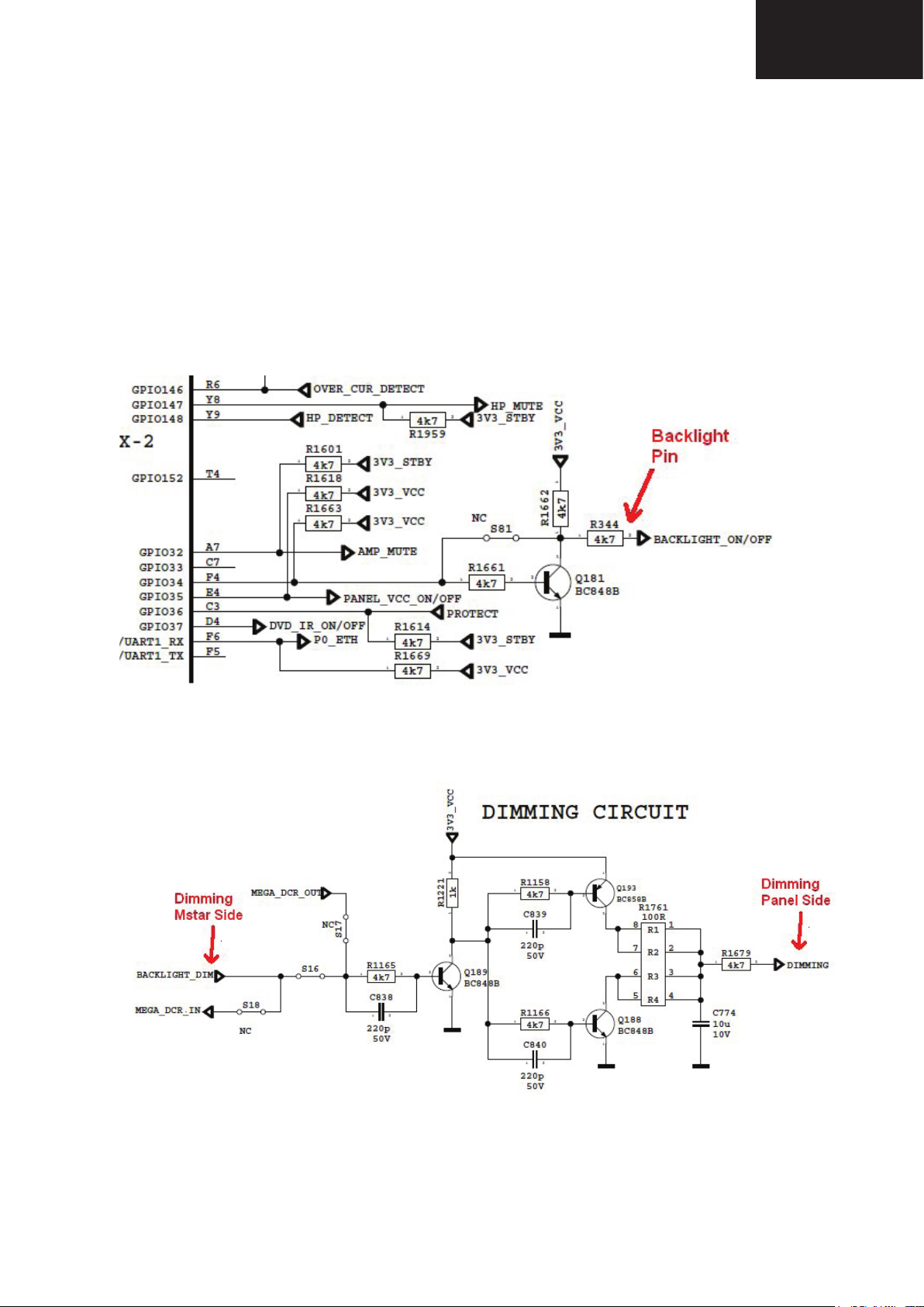
26. TROUBLESHOOTING
TROUBLESHOOTING
26. TROUBLESHOOTING
26.1. No Backlight Problem
Problem: If TV is working, led is normal and there is no picture and backlight on the panel.
LC-32LE510
LC-40LE510
Possible causes: Backlight pin, dimming pin, backlight supply, stby on/off pin
Backlight pin should be high in open position. If it is low, please check Q181 and panel cables.
Dimming pin should be high or square wave in open position. If it is low, please check S16 for Mstar side
and panel or power cables, connectors.
Backlight power supply should be in panel specs. Please check CN705 for MB60, related connectors for
power supply cards.
77
Page 78

LC-32LE510
LC-40LE510
STBY_ON/OFF should be low for standby on condition, please check R1677.
78
Page 79

26.2. CI Module Problem
26.2 CI Module Problem
Problem: CI is not working when CI module inserted.
LC-32LE510
LC-40LE510
Possible causes: Supply, supply control pin, detect pins, mechanical positions of pins
CI supply should be 5V when CI module inserted. If it is not 5V please check CI_POWER_CTRL, this pin
should be low.
Please check mechanical positions of CI module.
Detect ports should be low. If it is not low please check CI connector pins, CI module pins and 3V3_VCC on
MB60.
79
Page 80

LC-32LE510
LC-40LE510
26.3. Led Blinking Problem
Problem: LED blinking, no other operation
This problem indicates a short on Vcc voltages. Protect pin should be logic high while normal operation.
When there is a short circuit protect pin will be logic low. If you detect logic low on protect pin, unplug
the TV set and control voltage points with a multimeter to find the shorted voltage to ground.
80
Page 81

26.4. IR Problem
Problem: LED or IR not working
Check LED card supply on MB60 chassis.
LC-32LE510
LC-40LE510
81
Page 82

LC-32LE510
LC-40LE510
Problem: Keypad or Touchpad is not working
Check keypad supply and KEYBOARD pin on MB60.
26.5. Keypad Touchpad Problems
82
Page 83

26.6. USB Problems
Problem: USB is not working or no USB Detection.
Check USB Supply, It should be nearly 5V. Also USB Enable should be logic high.
LC-32LE510
LC-40LE510
83
Page 84

LC-32LE510
LC-40LE510
Problem: No audio at main TV speaker outputs.
Check supply voltages of VDD_AUDIO, 5V_VCC and 3V3_VCC with a voltage-meter.
There may be a problem in headphone connector or headphone detect circuit (when headphone is
connected, speakers are automatically muted). Measure voltage at HP_DETECT pin, it should be 3.3v.
26.7. No Sound Problem
26.8. No Sound Problem at Headphone
Problem: No audio at headphone output.
Check HP detect pin, when headphone is. Check 5V_VCC and 3V3_VCC with a voltage-meter.
26.9. Standby On/Off Problem
Problem: Device cannot boot, TV hangs in standby mode.
There may be a problem about power supply. Check 12V_VCC, 5V_VCC and 3V3_VCC with a voltagemeter. Also there may be a problem about SW. Try to update TV with latest SW. Additionally it is good to
check SW printouts via hyper-terminal (or Teraterm). These printouts may give a clue about the problem.
84
Page 85

LC-32LE510
LC-40LE510
26.11. No Signal Problem
26.10 No Signal Problem
Problem: No signal in TV mode.
Check tuner supply voltage; 5V_TUN. Check tuner options are correctly set in Service menu. Check AGC
voltage at RF_AGC pin of tuner.
85
Page 86

LC-32LE510
LC-40LE510
Notes:
86
Page 87

OVERAL WIRING DIAGRAM
GND
23
PANEL_VCC
DIM_PWM_ANALOG
4V25_STBY
24
GND25VCC_AUDIO
ST_BY2
CN140
CN703
MB60 / PW07 OVERALL WIRING DIAGRAM
27. OVERAL WIRING DIAGRAM
LC-32LE510
LC-40LE510
Overal wiring Diagram LC-32LE510
MODEL
MAIN BOARD
POWER SUPPLY
LC-32LE510E
MB60
PW07
PANEL INVERTER BOARD
PL306 CN706 CN137
PW07 POWER SUPPLY BOARD
1
24V
2
24V
3
24V
4
24V
5
24V
6
GND
7
GND
8
GND
9
GND
10
A/D_DIM_SEL
11
DIM_PWM_ANALOG
12 BL_ON/OFF_1 12 5V_VCC 12 TX_A_2_P
PL205
1
GND
2
GND
3
SW_SWITCH
4
GND
5
ST_BY
6
GND
7
BL_ON/OFF
8
9
10
GND
11
12V_1
12
12V_1
13
5VSTBY
14
24V_1
15
4V25_STBY
16
17
VCC_3V3_ON
18
5V
19
VCC_3V3_ON
20
5V
21
VCC_3V3_ON
22
5V
23
GND
INVERTER CABLE
PANEL T-CON BOARD
POWER
CABLE
LVDS CABLE
1 GND 1 GND
2 GND 2 GND
3 STBY_ON_OFF 3 GND
4 GND 4 GND
5 BACKLIGHT_ON_OFF 5 GND
6 GND 6 TX_A_3_P
7 DIMMING 7 TX_A_3_N
8 GND 8 GND
9 5V_STBY 9 TX_A_CLK_ P
10 12V_VC C 10 TX_A_CLK_N
11 5V_VCC 11 GND
13 12V_ST BY 1 3 TX_A_2_ N
14 12V_ST BY 1 4 GND
15 3V3_VC C 15 TX_A_1_P
16 5V_VCC 16 TX_A_1_N
17 3V3_VC C 17 GND
18 5V_VCC 18 TX_A_0_P
19 3V3_VC C 19 TX_A_0_N
20 5V_VCC 20 GND
21 PANEL_ VCC
22 PANEL_ VCC
24 GND
25 GND
26 GND
27 PANEL_ VCC
28 PANEL_ VCC
29 PANEL_ VCC
30 PANEL_ VCC
MB60 MAIN BOARD
ROCKER
SWITCH
PL701PL100
AC
POWER
PLUG
SPEAKER RIGHT
26
27
28
A/D_DIM_SEL
A/D_DIM_SEL
SPEAKER CABLE
LED IR BOARD
1 GND
2 LED 2
3 LED 1
4 IR_IN
5 5V_STBY
87
SPEAKER LEFT
1 R_AUDIO_P
2 R_AUDIO_N 1 GND
3 L_AUDIO_P 2 LED 2
4 L_AUDIO_N 3 LED 1
4 IR_IN
5 5V_STBY
LED/IR CABLE
Page 88

LC-32LE510
87654321
LC-40LE510
SCHEMATIC DIAGRAMS
28. Schematic Diagrams
Tuner & T2 Demodulator Diagram
1 2 3 4 5 6 7 8
5V_TUN5V_TUN
A
B
OVER_CUR_DETECT
C
D
E
F
AIF
12
DIF1
11
DIF2
10
IF_AGC
9
AS
8
NC
7
B2
6
SDA
5
SCL
RF_AGC
ANT_PWR
4
3
B1
2
1
TU102 TDTC-G101D
R1594
20k
R1586
3V3_VCC
10k
ANALOG_IF
2
1
120nH
C904
100n
10V
L115
22u
21
16V
C2
21
1u
C964
IF_AGC_TUNER
150p
47p
12
11
10
9
8
7
6
5
4
C3
22u
16V
RF_AGC_TUNER
330R
F261
2
100n
1
10V
C907
TH1
5V_TUN
2R1
R1595
10k
3
2
1
R1581
FDN336P
Q175
C965
100n
16V
10k
R1593
10k
BC848B
R4
50V
5V_TUN
5V_TUN
1k
Q172
C1211
21
47p
12V_VCC
DIGITAL_IF_P
N.C.
50V
DIGITAL_IF_N
R1591
10k
R1588
100R
8
R1
7
R2
6
R3
5 4
R4
R1592
10k
R1590
10k
1
2
3
3V3_VCC
TUN_SDA_MST
TUN_SDA_T2
TUN_SCL_MST
TUN_SCL_T2
3V3_VCC
RF_AGC_MST
ANT_CTRL
RF_AGC_CTL
R1551
100R
IF_AGC_MST
IF_AGC_T2
5V_TUN
6k8
R1598
21
F263
330R
F134
330R
C15V
2V5_VCC
C957
22u
16V
100n
10V
C920
F269
330R
C956
21
22u
16V
D5
F264
330R
100n
10V
C929
100n
10V
C931
F267
330R
100n
10V
C916
C15V
21
D6
F265
330R
C15V
21
D2
F262
330R
C932
C917
100n
10V
100n
10V
100n
C933
2V5_AVDD
3V3_RVDD
10V
100n
C921
100n
10V
C927
1V2_PVDD
100n
10V
C935
10V
100n
10V
C928
3V3_DVDD
100n
10V
C922
100n
10V
C925
1V2_MVDD1V2_VCC
R1589
12k
100n
10V
C919
R1939
10k
R1546
100R
R1545
100R
2
1
R1550
C901
100n
10V
100n
10V
C923
2
100R
21
R1597
10k
21
3
Q207
BC848B
1
21
C903
2
100n
1
10V
2
1
NC
B0 A
FSA3157
GND
2
B1
1
RF_AGC_CTL
R1552
100R
C912
100n
10V
S28
U3
VCC
21
IF_AGC_TUNER
C910
2
100n
1
10V
5V_TUN
1
2
R1934
2
1
10k
2
1
100k
C14
10V
100n
2
5V_VCC
3
1
2
1
100k
R1933
R1549
100R
Q205
BC848B
R1932
100k
43
5
S
6
R1596
12V_VCC
RF_AGC_MONITOR
21
RF_AGC_TUNER
C902
2
100n
1
10V
5V_TUN
ANALOG_IF
S100
R138
1k
R139
1k
C545
47p
50V
C955
F266
330R
82p
2413
150nH
L124
10n
C1210
47p
50V
50V
12p
X1
16V
21
47u
C546
10n
16V
21
2 1
C143
50V
12p
4k7
R252
1k
R1582
C954
C135
100n
2
1
R1857
2V5_VCC
10V
200R
0R
R483
1k2
1u
L114
680R
R735
2 1
2 1
R1580
21
2
3
1
21
R384
10R
Q144
BF799
47R
0R
C547
10n
16V
3V3_DVDD
41MHz
1V2_CVDD
DIGITAL_IF_N
DIGITAL_IF_P
S97
S96
TUN_SDA_T2
TUN_SCL_T2
C918
100n
10V
2V5_AVDD
3V3_RVDD
1V2_CVDD
3V3_DVDD
1V2_CVDD
C915
100n
10V
10k
R1566
49
AINM
50
AINP
51
AVSS1
52
AVDD1
53
RFAIN
54
RVDD
55
VSS8
56
CVDD6
57
TUNERDAT
58
TUNERCLK
59
DVDD
60
VSS9
61
CVDD
62
PLLBPN
63
RFAGC_GPIO1
64
IFAGC
1V2_PVDD
600R
F260
44
45
46
47
48
XVSS
XTALI
XTALO
XVDD
PVDD
T2 DEMOD
GPIO0
TSERR_GPIO2
TSSYNC
TSVALID
TSCLK
5
4
3
2
1
1V2_MVDD
41
42
43
PVSS
MVSS4
MVDD4
U167
CXD2820R
VSS1
CVDD1
MVDD1
8
7
6
40
MVDD3
MVSS1
9
39
MVSS3
VSS2
10
10k
R1564
38
OSCMODE
DVDD1
11
37
RESETN
TSDATA0
12
IF_AGC_T2
47R
47R
10V
100n
C911
33R
R1578
33R
R1573
33R
47R
R1579
1V2_CVDD
C953
12p
50V
TSMIVALID
TSMISYNC
1V2_MVDD
TSMICLK
3V3_DVDD
VESTEL
SCH NAME :
DRAWN BY :
21
R473
21
21
SIF_CTL
21
1V2_CVDD
36
CVDD5
TSDATA1
13
6k8
6k8
35
14
21
2K7
3k3
R231
5V_TUN
R474
22k
R594
2 1
10k
R1565
10V
C914
100n
33
34
A0
VSS7
OSCENBN
CVDD2
VSS3
TSDATA2
16
15
1V2_CVDD
MB60_HW_TEAM
2 1
2
D145
BA782
2
R209
2
1
1
100k
3
2
3V3_DVDD
RESET_T2
47R
R1856
R1560
10k
R1561
10k
32
TESTMODE
31
VSS6
30
CVDD4
29
SDA
28
SCL
27
DVDD2
26
VSS5
25
TSDATA7
24
TSDATA6
23
TSDATA5
22
TSDATA4
21
VSS4
20
CVDD3
19
MVDD2
18
MVSS2
17
TSDATA3
PROJECT NAME :
Z101
IN1 OUT1
K9656M
IN2
OUT2
GND
3
Q140
BSN20
Z102
IN1 OUT1
K3958M
IN2
OUT2
GND
3
3V3_DVDD
1V2_CVDD
R1576
R1575
3V3_DVDD
5 4
6
7
8
R1584
R1583
47R
R4
5 4
R3
6
R2
7
R1
8
17mb60-4
41
5
41
5
47R
47R
33R
R4
R3
3
R2
2
R1
1
47R
1V2_CVDD
1V2_MVDD
33R
3
2
1
TOTAL SHEET:
24-05-2011_13:42
21
L104
TS_MDI3
TS_MDI2
TS_MDI1
TS_MDI0
SIFP
SIFM
2u2
SDA_SYS
SCL_SYS
TS_MDI7
TS_MDI6
TS_MDI5
TS_MDI4
A
VIFM
B
VIFP
C
D
E
F
A3
9TUNER&T2_DEMOD
AX M
88
Page 89

Peripherals Diagram
1 2 3 4 5 6 7 8
SCART
A
B
C
D
DVD_SENSE
E
F
SC1
SCART LT1
DVD_Y_IN 180R
21
10V
4k7
C628
100n
2 1
R1616
DVD_SPDIF
12V_VCC
IPOD_R_IN IPOD_L_IN
100R
SDA_SYS
SCL_SYS
RX/SCL_SC
TX/SDA_SC
21
321
D175
5
4
NUP4004M5
321
NUP4004M5
20
19
18
17
16
15
14
13
12
4
D174
5
21
C835
50V
220p
2 1
R1233
220R
50V
220p
2 1
C833
2 1
R1481
75R
2 1
R1482
220p
75R
50V
C836
75R
R1479
2 1
47R
2 1
R1249
SC_R
TX/SDA_SC
SC_CVBS_IN
C860
11
75R
50V
C853
3n3
2 1
R1483
R1187
10
9
8
7
6
5
D178
2 1
C15V
50V
220p
2 1
C831
75R
2 1
R1489
SCART_AUD_L_IN
4
3
SCART_AUD_R_IN
2
1
F201
600R
C854
F206
600R
3n3
21
50V
21
C858
4n7
R1245
50V
100R
21
21
22k
F205
600R
F200
600R
SC_AUD_R_IN
SC_AUD_R_OUT
RX/SCL_SC
21
21
SC_B
SC_AUD_L_IN
R1244
100R
C857
4n7
50V
DVD INTERFACE (for 26" to 32")
1
R1624
100R
R1623
TP42
TP4
100R
R1652
R1650
21
75R
TP44
TP38
CN704
1
1
1
50V
220p
C972
109
R1653
75R
50V
27p
R1651
180R
1
TP39
1
TP5
1
1
TP1
21
C650
21
43
65
87
C973
TP43
DVD_IR
DVD_C_IN
25V
10u
S80
!
FS1
4A/24VDC
21
DVD_WAKEUP
C18V
21
1
IPOD INTERFACE
30 29
28 27
26 25
S79
S78
24 23
22 21
IPOD_Y_IN IPOD_C_IN
F199
2 1
600R
MAIN_R MAIN_L
R1938
56R
8
1
R1
7
2
R2
6
3
R3
54
R4
20 19
18 17
16 15
14 13
12 11
10 9
8 7
6 5
4 3
2 1
AMP_MUTE
F198
600R
CN133
NC
F207
600R
21
C824
27p
50V
21
21
21
21
12V_VCC
5V_STBY
IPOD_DETECT
IR_IN
1n
50V
D181
TP242
220p
C832
R1182
21
12V_VCC
SC_FB
R1480
2 1
2 1
4k7
100n
SC_CVBS_OUT
75R
50V
21
2 1
10V
C664
SC_AUD_L_OUT
SC_G
SC_PIN8
SCART VIDEO OUTPUT AMPLIFIER
12V_VCC
R124
470R
220R
SC_CVBS_OUT
330R
21
C120
10u
16V
1
Q146
BC858B
R1587
75R
2
3
R620
300R
F179
C788
12p
NC
50V
INDIA OPTION
VGA_R
VGA_G
VGA_B
VGA_G
SC_R
SC_G
SC_B
SC_CVBS_IN
RCA_PR
RCA_Y
RCA_PB
RCA_Y
R1420
33R
R1422
33R
R1421
33R
VGA_HSNC
VGA_VSNC
R1507
33R
R1510
33R
R1509
33R
R1506
33R
R1508
33R
R1511
33R
R1409
R1408
R1419
R1423
R1505
33R
SC_FB
R1494
33R
33R
33R
470R
470R
R1418
33R
R1417
33R
R1416
33R
C862
R1407
33R
R1405
33R
R1406
33R
SC_CVBS_IN
SCART_AUD_L_IN
SCART_AUD_R_IN
47n
16V
C808
47n
16V
C810
47n
16V
16V
C809
47n
16V
C861
1n 50V
C882
16V
47n
16V
16V
C885
47n
47n C797
16V
C884
47n
16V
1n 50V
16V
C881
47n
16V
16V
C883
47n
16V
16V
C886
47n
16V
C859
1n
50V
C807
16V
C806
47n
C802
47n
C798
47n
16V
C796
47n
C805
47n
C803
47n
C804
47n
M2
M3
L2
L3
K1
K3
K2
N4
N5
R3
P2
P3
N2
N3
M1
N1
W6
Y6
U2
U3
T2
T1
R1
R2
T3
V4
4
YEL
3
WHT
2
RED
1
RIN0M
RIN0P
GIN0M
GIN0P
BIN0M
BIN0P
SOGIN0
HSYNC0
VSYNC0
RIN1M
RIN1P
GIN1M
5
U157
GIN1P
MSD9WB7PX-2
BIN1M
BIN1P
SOGIN1
HSYNC1
VSYNC1
RIN2M
RIN2P
GIN2M
GIN2P
BIN2M
BIN2P
SOGIN2
HSYNC2
JK7
CVBS0
CVBS1
CVBS2
CVBS3
CVBS4
CVBS5
CVBSOUT0
CVBSOUT1
BC848B
21
VCOM
Q119
R102
AC5
W4
W5
AA5
W2
W3
V3
AA4
W1
68k
R103
390R
3
2
1
33k
R104
R221
100R
2 1
16V
C795
47n
16V
47n
16V
C801
47n
16V
47n
16V
C794
47n
16V
47n
SCART_CVBS_OUT
16V
47n
C959
33R
R1530
C378
10u
10V
12K
R1415
33R
C800
R1414
33R
C799
R1411
33R
C793
IR_IN
DVD_IR_ON/OFF
SCART_CVBS_OUT
R1413
33R
R1412
33R
R1410
33R
75R
R1484
2 1
BC848B
1
21
R498
75R
2
1
2
47k
R1485
Q157
75R
3
CN132
R1486
2 1
R12
15
14
13
12
11
10
9
8
7
6
5
4
3
2
1
R11
270R
270R
DVD_IR
R694
2 1
4k7
VGA_DDC_5V
close to vga
connector!!
SC_CVBS_IN
DVD_Y_IN
DVD_C_IN
SAV_CVBS_IN
IPOD_C_IN
S93
IPOD_Y_IN
JK2
3V3_VCC
4k7
R263
2 1
321
NUP4004M5
2k2
2k2
2K7 2K7
R1209
2 1
R15
75R
R10
21
75R
R9
21
75R
SC_R
21
SC SVHS opt
7
5
4
3
6
2
1
PC INPUT
D176
R1311
5
4
R1206
2 1
21
321
JK3
21
S103
21
S102
21
S101
JK4
YEL
WHT
RED
5V_VCC
21
1
TP13
21
21
21
10k
10k
10k
R1310
R1265
R1243
2
1
R1949
100R
C663
100n
10V
100R
3
D169
BAV70
VGA_DDC_5V
21
21
VGA_VSNC
VGA_HSNC
VGA_B
VGA_G
5
4
D173
NUP4004M5
1
2
75R
75R
75R
R1516
R1515
2 1
R1517
2 1
2 1
SIDE AV INPUT
1
TP245
6
3
4
5
7
D171
1
TP250
SAV_L
1
TP247
C5V6
F203
600R
F202
600R
C830
21
21
2 1
220p
50V
SAV_R
YPbPr INPUT
1
TP246
1
TP248
321
5
4
D177
NUP4004M5
50V
27p
C8292127p
50V
21
C823
RCA SAV INPUT opt.
SAV_CVBS_IN
21
6
5
4
3
2
1
VESTEL
SCH NAME :
DRAWN BY :
S9
21
S42
21
S39
PROJECT NAME :
MB60_HW_TEAM
SAV_L
SAV_R
VGA_B
VGA_G
VGA_R
VGA_R
SAV_CVBS_IN
50V
C856
3n3
SAV_L_IN
SAV_R_IN
C855
3n3
50V
1
TP249
21
50V
C828
27p
75R
R1619
2 1
17mb60-4
TOTAL SHEET:
24-05-2011_13:43
87654321
75R
2 1
75R
R1620
2 1
R1621
LC-32LE510
LC-40LE510
A
B
C
D
RCA_PR
RCA_Y
RCA_PB
E
F
A3
9PERIPHERALs
AX M
89
Page 90

LC-32LE510
LC-40LE510
GPIOs & USB & LVDS Out Diagram
1 2 3 4 5 6 7 8
CFG_PWM0
3V3_VCC
BACKLIGHT_DIM
3V3_STBY
A
KEYBOARD
DVD_SENSE
RF_AGC_MONITOR
DVD_WAKEUP
3V3_STBY
NC
3V3_VCC
B
SCL_SYS
SDA_SYS
C952
18p
C
C951
18p
RESET
D
RESET
3V3_STBY
E
F
CFG_PWM1
R1615
2 1
4k7
SC_PIN8
R1
4k7
2 1
4k7
R1524
2 1
IR_IN
50V
1M
R1533
50V
USB_DP
USB_DM
21
R1528
R1522
2 1
R1523
SPI_CSN_1
SPI_SCK
SPI_SDI_1
SPI_SDO
FLASH_WPN
RX/SCL_SC
TX/SDA_SC
4k7
R1527
2 1
2 1
X2
24MHz
2 1
USB_DP_ETH
USB_DM_ETH
USB_DP
USB_DM
R1668
1k
C1016
D189
1N4148
4k7
4k7
4k7
R1667
R1543
100R
100R
R8
100R
R7
100R
2 1
R1666
21
10k
R844
2 1
R845
2 1
USB_OCD
NC
21
NC
100n
10R
10R
21
10V
2
1
C1031
22u
16V
C1015
100n
10V
AB25
AB24
AA23
AA24
AD11
AE11
PWM0
PWM1
E6
PWM2
D6
PWM3
J5
SAR0
G4
SAR1
B4
SAR2
AA7
SAR3
C4
GPIO12
A4
SCZ
A2
SCK
B3
SDI
A3
SDO
B2
GPIO14
P6
DDCA_CK/UART0_RX
N6
DDCA_DA/UART0_TX
DDCR_CK
DDCR_DA
G5
IRIN
AD1
XIN
AE2
XOUT
E5
HWRESET
C2
USB0_DP
B1
USB0_DM
USB1_DP
USB1_DM
F11
GND0
E11
GND1
GPIO139/SPDIFI
4
U157
MSD9WB7PX-2
GPIO44/UART1_RX
GPIO45/UART1_TX
LVB0P
LVB0M
LVB1P
LVB1M
LVB2P
LVB2M
LVBCKP
LVBCKM
LVB3P
LVB3M
LVB4P
LVB4M
LVA0P
LVA0M
LVA1P
LVA1M
LVA2P
LVA2M
LVACKP
LVACKM
LVA3P
LVA3M
LVA4P
LVA4M
GPIO137
GPIO138
GPIO140
GPIO141
GPIO142
GPIO143
GPIO144
GPIO146
GPIO147
GPIO148
GPIO152
GPIO32
GPIO33
GPIO34
GPIO35
GPIO36
GPIO37
GPIO6
GPIO7
GPIO10
GPIO11
GPIO17
GPIO18
AC24
AC25
AD24
AD25
AE24
AC23
AE23
AD23
AE22
AC22
AC21
AD22
AC20
AD21
AE20
AD20
AE19
AC19
AC18
AD19
AC17
AD18
AE17
AD17
AA10
T5
AB10
AB7
AA9
V5
AC11
AA8
R6
Y8
Y9
T4
A7
C7
F4
E4
C3
D4
F6
F5
AB8
H5
C5
K4
L5
M6
R1604
RESET
USB INTERFACE
U145
47k
IO4
VDD
R809
2 1
6
5
4
4k7
5V_VCC
1
OUT
2
GND
STMP2161
FAULT EN
U149
IN
C610
10u
10V
4
3
2
1
CN128
5
43
1
IO1
2
GND
AZ099-04S
IO23IO3
R1201
21
100k
R884
TX_B_0_P
TX_B_0_N
TX_B_1_P
TX_B_1_N
TX_B_2_P
TX_B_2_N
TX_B_CLK_P
TX_B_CLK_N
TX_B_3_P
TX_B_3_N
TX_B_4_P
TX_B_4_N
TX_A_0_P
TX_A_0_N
TX_A_1_P
TX_A_1_N
TX_A_2_P
TX_A_2_N
TX_A_CLK_P
TX_A_CLK_N
TX_A_3_P
TX_A_3_N
TX_A_4_P
TX_A_4_N
USB_ENABLE
IPOD_DETECT
DVD_SPDIF
PCM_CD1_N
USB_OCD
RESET_T2
R1659
21
4k7
OVER_CUR_DETECT
HP_DETECT
R1601
4k7
R1618
4k7
R1663
4k7
PANEL_VCC_ON/OFF
DVD_IR_ON/OFF
P0_ETH
CI_POWER_CTRL
R1607
18k
R1606
33k
33k
4k7
R1605
R1617
R1672
2 1
3V3_STBY
USB
5V_VCC
R1198
47k
USB_ENABLE
SW3
R1499
R1656
3V3_VCC
21
3V3_STBY
21
3V3_VCC
21
3V3_VCC
AMP_MUTE
18k
4k7
2 1
3V3_STBY
5V_VCC
21
4k7
SW4
10k
270R
R1294
NC
21
21
4k7
R1959
PROTECT
R1614
21
4k7
R1669
21
4k7
R1952
21
4k7
HDMI0_5V
STBY_ON/OFF_NOT
HDMI1_5V
LED1
LED2
4k7
R1671
2 1
3V3_STBY
SW2
21
R1498
STBY_INFO
3V3_STBY
HP_MUTE
3V3_STBY
NC
S81
R1661
4k7
3V3_STBY
3V3_VCC
3V3_VCC
1k2
LED SOCKETONBOARD KEYBOARD
LED1
TX_B_0_N
TX_B_0_P
TX_B_1_N
TX_B_1_P
TX_B_2_N
TX_B_2_P
TX_B_CLK_N
TX_B_CLK_P
TX_B_3_N
TX_B_3_P
TX_A_0_N
TX_A_0_P
5
4
3
2
Q170
BC848B
3
1
CN703
R1563
1
10k
BC858B
21
220R
2
R1940
3
1
21
220R
21
220R
R1571
Q174
Q173
R1569
C949
27p
50V
21
21
220R
3
1
21
220R
F259
600R
R1562
R1572
2
BC858B
R1570
5V_STBY
21
Q171
10k
BC848B
IR_IN
3
1
R1568
2
10k
TP10
1
STBY+ - P/VOL
SW1
21
2k7
R1497
KEYBOARD_ONBOARD
21
3V6 lik zener kullanilmali
C15V
D204
R1567
10k
2
LED2
5V_STBY
TX_A_1_N
TX_A_1_P
TX_A_2_N
TX_A_2_P
OPTION2
10k
2 1
21
S14
TX_A_CLK_N
TX_A_CLK_P
PANEL_VCC
PANEL_VCC
21
S19
R1280
21
S13
TX_A_3_N
TX_A_3_P
S15
2 1
2 1
S32
2 1
S33
PANEL_VCC
21
S30
10k
2 1
3V3_VCC
21
4k7
R1662
R344
21
4k7
3
2
21
Q181
BC848B
1
BACKLIGHT_ON/OFF
TOUCH_PAD_OPTION
MECH_SWITCH
S76
R793
2
1
CN702
2
1
CN709
EXT KEYPAD
KEYBOARD_ONBOARD
F248
21
47R
3
3
600R
4
R1937
47R
6
5
4
21
F249
600R
21
R1936
47R
C630
2
100n
1
10V
21
SCL_SYS
21
PANEL_VCC
KEYBOARD
3V3_STBY
SDA_SYS
MEGA_DCR_IN
21
S56
21
21
PANEL_VCC
S3
S99
PANEL VCC = 5V/12V
9
8
7
6
5
4
3
2
1
CN138
12
11
10
30
29
28
27
26
25
24
23
22
21
20
19
TX_B_CLK_N
TX_B_CLK_P
18
17
16
15
14
13
12
11
10
9
8
TX_A_CLK_N
7
6
5
4
3
2
19" TO 22" DOUBLE LVDS FFC OPTIONS
1
CN139
SINGLE LVDS FFC OPTIONS
OPTION1
MEGA_DCR_OUT
21
R1300
S58
TX_A_3_N
TX_A_3_P
14
13
15
TX_A_CLK_P
16
TX_A_CLK_N
18
17
TX_A_2_P
TX_A_2_N
20
19
TWISTED PAIR LVDS OPTION
TP21
CN136
TP23
TP19
TP17
TP16
TP18
TP20
TP22
TP24
TP26
TP28
TP25
TP30
TP27
TP29
TP31
TP34
TP33
TP35
TP32
TX_A_1_N
TX_A_1_P
23
22
1
1
1
1
1
1
1
24
1
1
1
1
1
1
1
1
1
1
1
1
1
S6
2 1
TX_A_0_P
25
21
43
65
87
109
1211
1413
1615
1817
2019
2221
2423
2625
2827
3029
3231
3433
3635
3837
4039
4241
4443
4645
4847
5049
PANEL_VCC
10k
R1295
2 1
TX_A_0_N
27
26
21
S55
OPTION5
28
1
1
2 1
OPTION1
OPTION2
OPTION3
1
TX_A_4_P
1
TX_A_4_N
PANEL_VCC
10k
R1297
R1296
2 1
30
29
TP9
TX_B_4_N
TP8
TX_B_4_P
PANEL_VCC
S57
10k
R1266
10k
2 1
R1301
S4
21
TP6
TP7
OPTION4
10k
2 1
21
S10
OPTION7
OPTION3
3V3_VCC
3V3_VCC
MEGA_DCR_OUT
21
S3621S34
10k
R1274
2 1
S94
TX_B_0_N
TX_B_0_P
TX_B_1_N
TX_B_1_P
TX_B_2_N
TX_B_2_P
TX_B_3_N
TX_B_3_P
TX_A_0_N
TX_A_0_P
TX_A_1_N
TX_A_1_P
TX_A_2_N
TX_A_2_P
TX_A_CLK_P
TX_A_3_N
TX_A_3_P
MEGA_DCR_IN
21
21
PANEL_VCC
PANEL_VCC
OPTION6
PANEL_VCC
A
B
C
D
E
PANEL_VCC = 5V/12V
9
8
7
6
5
4
3
2
PANEL_VCC
1
CN137
S2
OPTION6
OPTION7
S12
2 1
S54
2 1
R1275
PANEL_VCC
TX_A_4_P
TX_A_4_N
S35
S37
2 1
2 1
2 1
S71
2 1
TX_A_3_P
S72
2 1
TX_A_CLK_P
TX_A_3_N
TX_A_CLK_N
10k
TX_A_2_P
TX_A_1_P
TX_A_2_N
21
TX_A_0_N
TX_A_1_N
TX_A_0_P
TX_B_4_P
S74
S73
2 1
2 1
TX_B_4_N
TX_B_3_P
TX_B_3_N
MEGA_DCR_OUT
TX_B_CLK_P
TX_B_CLK_N
5150494847464544434241403938373635343332313029282726252423222120191817161514131211
TX_B_2_P
TX_B_2_N
TX_B_1_P
TX_B_1_N
TX_B_0_P
TX_B_0_N
10
21
OPTION3
S98
OPTION5
OPTION4
OPTION2
OPTION1
987654321
10
27
26
25
24
23
22
21
20
19
18
17
16
15
14
13
12
11
21
S11
CN135
SCH NAME :
DRAWN BY :
VESTEL
MB60_HW_TEAM
PROJECT NAME :
17mb60-4
24-05-2011_13:43
87654321
30
29
28
TOTAL SHEET:
F
A3
9GPIOs&USB&LVDS_OUT
AX M
90
Page 91

87654321
Audio IO & HDMI Inputs Diagram
1 2 3 4 5 6 7 8
AUDIO OUTPUTs
4k7
R1900
4k7
R1899
A
22K
33n
C1183
MAIN_R
C1184
4k7
33n
R1898
10n
10n
16V
16V
100R
4k7
R1897
100R
22K
C1168
HP_L DSP_HP_L
2 1
100u
16V
B
C1169
HP_R
SC_L_OUT
C
SC_R_OUT
2 1
100u
16V
HPL_MUTE
L119
10u
220R
200R
R1858
C1170
10u
10V
HPR_MUTE I2S_OUT_SD
L120
10u
220R
200R
R1859
C1171
10u
10V
R223
2 1
C1185
C1186
100R
16V
10n
R222
2 1
100R
16V
10n
21
22k
R1924
21
22k
R1925
AUDIO INPUTs
SC_AUD_R_IN
D
SC_AUD_L_IN
SAV_R_IN
E
SAV_L_IN
IPOD_R_IN
F
IPOD_L_IN
R1902
10k
R1901
10k
R1903
10k
R1904
10k
R1906
10k
R1905
10k
12k
R1921
12k
R1920
12k
R1918
12k
R1919
12k
R1923
12k
R1922
C1187
C1188
C1189
C1190
C1192
C1191
SCART_AUDIO_IN_R
50V
470p
SCART_AUDIO_IN_L
50V
470p
SAV_AUDIO_IN_R
50V
470p
SAV_AUDIO_IN_L
50V
470p
IPOD_AUDIO_IN_R
50V
470p
IPOD_AUDIO_IN_L
50V
470p
DSP_MAIN_LMAIN_L
DSP_MAIN_R
DSP_HP_R
DSP_SCART_L
DSP_SCART_R
SCART_AUDIO_IN_L
SCART_AUDIO_IN_R
SAV_AUDIO_IN_L
SAV_AUDIO_IN_R
IPOD_AUDIO_IN_L
IPOD_AUDIO_IN_R
C1198
C1195
C1194
10u
10u
10u
10V
10V
10V
DSP_MAIN_L
DSP_MAIN_R
DSP_SCART_L
DSP_SCART_R
DSP_HP_L
DSP_HP_R
C1199
10u
2 1
2 1
4k7
R1674
3V3_VCC
10V
R1892
4k7
C1201
1u
6V3
I2S_OUT_MCK
I2S_OUT_BCK
RST_ETH
TP223
2 1
4k7
R1894
ANT_CTRL
3V3_VCC
C1174
2
100n
1
10V
3V3_VCC
WAKEUP_ETH
SPDIF_OUT
MODE SELECTION
I2S_OUT_SD
CFG_PWM0
I2S_OUT_MCK
I2S_OUT_BCK
10k
R1840
CFG_PWM1
10k
R1833
3V3_STBY
1:NAND
10k
R1838
NC
0:IPS
10k
R1839
10k
R1836
10k
R1835
C1197
10u
C1196
10u
C1193
10u
10V
10V
10V
C1200
4u7
10V
1
R4
R5
T6
U6
V6
U5
AD6
AC6
V1
V2
AA6
Y5
AD5
AE5
AB4
AB5
AC3
A6
B5
B6
C6
C1
H6
G6
P5
SC_R_OUT
AUL0
AUR0
AUL1
AUR1
AUL2
AUR2
AUL3
AUR3
AUOUTL0
AUOUTR0
AUOUTL1
AUOUTR1
EAR_OUTL
EAR_OUTR
AUVRP
AUVAG
AUVRM
I2S_OUT_MCK
I2S_OUT_SD
I2S_OUT_WS
I2S_OUT_BCK
I2S_IN_BCK
I2S_IN_SD
I2S_IN_WS
SPDIFO
SC_AUD_R_OUT
3
U157
MSD9WB7PX-2
C1203
1u
6V3
JK10
G2
RXA0N
RXA0P
RXA1N
RXA1P
RXA2N
RXA2P
RXACKN
RXACKP
DDCDA_CK
DDCDA_DA
HOTPLUGA
RXB0N
RXB0P
RXB1N
RXB1P
RXB2N
RXB2P
RXBCKN
RXBCKP
DDCDB_CK
DDCDB_DA
HOTPLUGB
RXC0N
RXC0P
RXC1N
RXC1P
RXC2N
RXC2P
RXCCKN
RXCCKP
DDCDC_CK
DDCDC_DA
HOTPLUGC
CEC
H3
H2
J3
J2
J1
G3
G1
M4
M5
K6
D2
E3
E2
F3
F2
F1
D3
D1
J6
L6
J4
AC8
AD9
AC9
AD10
AE10
AC10
AE8
AD8
AE7
AD7
AC7
K5
HDMI_1_RX0N
HDMI_1_RX0P
HDMI_1_RX1N
HDMI_1_RX1P
HDMI_1_RX2N
HDMI_1_RX2P
HDMI_1_CLKN
HDMI_1_CLKP
HDMI_1_SCL
HDMI_1_SDA
HDMI_0_RX0N
HDMI_0_RX0P
HDMI_0_RX1N
HDMI_0_RX1P
HDMI_0_RX2N
HDMI_0_RX2P
HDMI_0_CLKN
HDMI_0_CLKP
R1917
2 1
10R
HDMI_0_SCL
HDMI_0_SDA
CEC
HDMI1_5V
21
4k7
R1896
2 1
HDMI0_5V
21
4k7
R1895
2 1
R1912
1k
R1911
1k
R1909
2 1
1k
R1910
2 1
1k
HDMI1_HPD
3
2
Q204
BC848B
1
HDMI0_HPD
3
2
Q203
BC848B
1
PRE-AMP for SCART AUDIO
33k
1
OUT1
U178
2
IN1-
TL062
3
IN1+
VSS IN2+
Q202
BC848B
S92
33k
21
R1915
21
33k
R1916
C1177
100n
16V
VDD
OUT2
IN2-
5V_VCC
3
1
21
12V_VCC
F301
2 1
600R
8
7
6
54
V+
21
4k7
R1889
C1175
2
21
21
100n
10V
4k7
R1890
R1913
C1205
100p
50V
R1926
82k
33k
21
50V
12V_VCC
21
2 1
220p
C1180
10u
10V
R1928
R1907
C1178
NC
100R
C1202
21
1u
6V3
21
SC_AUD_L_OUT
SPDIF_OUT
C1181
R1929
20k
10u
10V
V+
C1206
100p
50V
R1927
82k
21
C1182
10u
10V
R1914
2 1
21
V+
COAX SPDIF OUT
50V
220p
NC
21
C1179
C5V6
C1176
21
21
21
100n
10V
1k
D199
R1908
NC
2
3
1
LC-32LE510
LC-40LE510
HDMI2
R1877
HDMI_0_RX2P
HDMI_0_RX2N
HDMI_0_RX1P
HDMI_0_RX1N
HDMI_0_RX0P
HDMI_0_RX0N
HDMI_0_CLKP
HDMI_0_CLKN
HDMI_0_SCL
HDMI_0_SDA
HDMI0_5V
HDMI0_HPD
2
2
1
2
CEC
HDMI1
HDMI_1_RX2P
HDMI_1_RX2N
HDMI_1_RX1P
HDMI_1_RX1N
HDMI_1_RX0P
HDMI_1_RX0N
HDMI_1_CLKP
HDMI_1_CLKN
CEC
HDMI_1_SCL
HDMI_1_SDA
HDMI1_5V
HDMI1_HPD
SC_L_OUT20k
VESTEL
SCH NAME :
DRAWN BY :
1
10R
R1869
2 1
10R
10R
1
R1868
R1887
2 1
10R
10R
2
R1867
R1886
2 1
10R
10R
1
R1879
R1880
2 1
10R
R1888
2 1
10R
2
10R
1
R1885
10R
2 1
R1878
R1874
1
10R
R1870
2 1
10R
10R
1
R1884
R1871
2 1
10R
10R
2
R1872
R1882
2 1
10R
10R
1
R1876
R1883
2 1
10R
R1873
2 1
10R
2
10R
1
R1875
10R
2 1
R1881
MB60_HW_TEAM
21
21
47k
47k
R1865
R1864
21
21
47k
47k
R1863
R1862
PROJECT NAME :
CN708
21
20
1
2
3
4
5
6
7
8
9
10
11
12
13
14
15
16
17
18
19
CN707
21
20
1
2
3
4
5
6
7
8
9
10
11
12
13
14
15
16
17
18
19
17mb60-4
TOTAL SHEET:
24-05-2011_13:43
A
B
COMMON OPTIONAL
C
D
E
F
A3
9AUDIO_IO&HDMI_INPUTs
AX M
91
Page 92
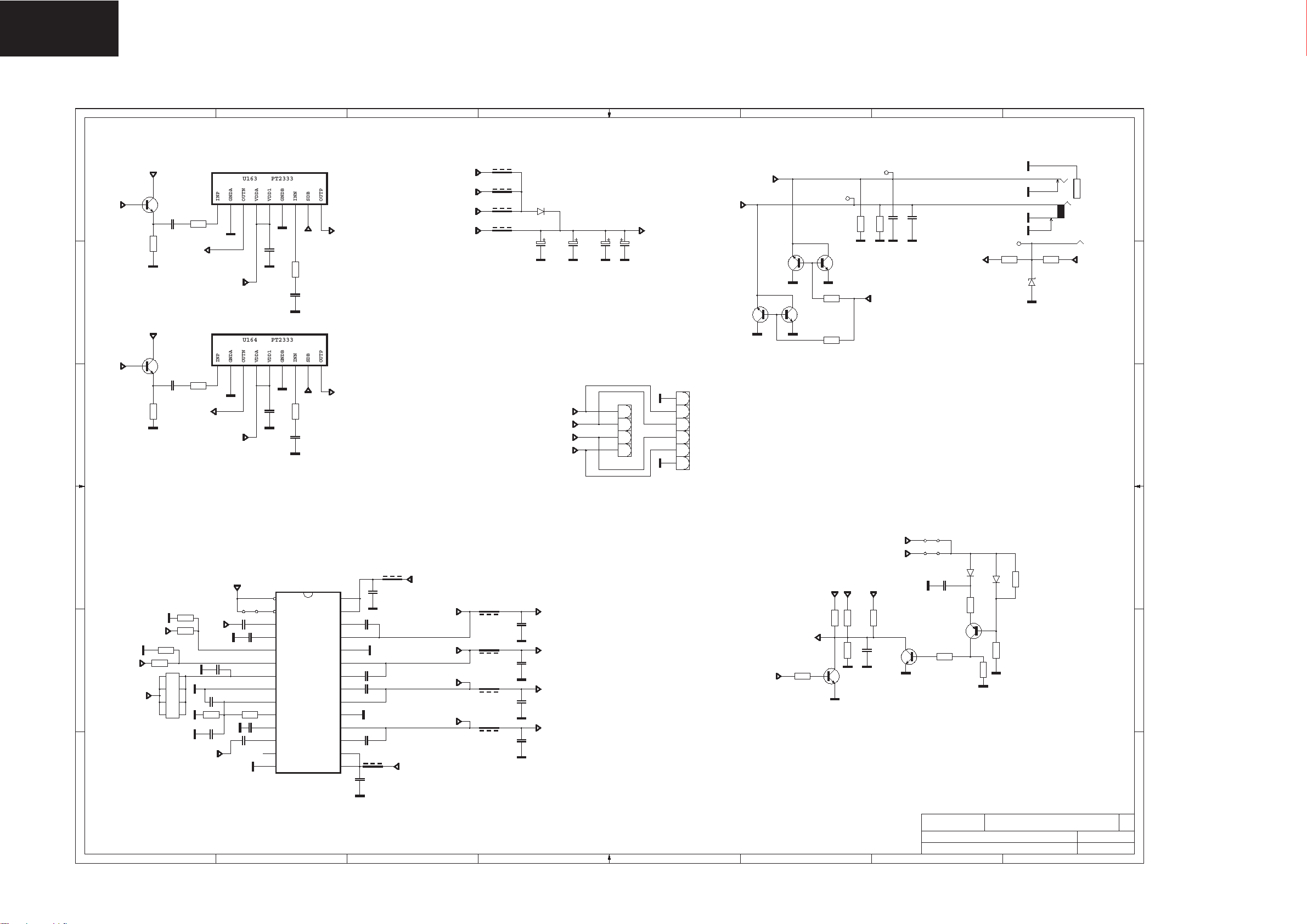
LC-32LE510
LC-40LE510
Audio AMP & HP AMP Diagram
1 2 3 4 5 6 7 8
AUDIO AMP for 16" to 24"
VDD_AUDIO
A
GNDA
MAIN_L
Q160
BC848B
C612
100n
10V
R817
100R
L_AUDIO_N_OUT
INP
A1A2A3B1B2B3C1C2C3
R623
15k
VDD_AUDIO
B
VDD_AUDIO
OUTN
C665
100n
10V
VDDA
PT2333U163
VDD1
2
1
GNDB
R624
C617
INN
15k
SDB
AMP_EN
10V
100n
OUTP
L_AUDIO_P_OUT
12V_VCC
24V_VCC
18V_VCC
5V_VCC
PT2333U164
MAIN_R
2
3
1
R818
BC848B
Q133
100R
C602
R613
15k
100n
10V
R_AUDIO_N_OUT
OUTN
GNDA
INP
A1A2A3B1B2B3C1C2C3
C
VDD_AUDIO
VDDA
C666
10V
100n
VDD1
2
1
GNDB
C608
R614
INN
15k
SDB
AMP_EN
10V
100n
OUTP
R_AUDIO_P_OUT
F283
60R
F285
60R
F284
60R
F294
60R
10V
220u
C615
D192
SK24
10V
220u
C870
W/2.5W opt.
R_AUDIO_P
R_AUDIO_N
L_AUDIO_P
L_AUDIO_N
35V
100u
C1208
CN140
1
2
3
4
35V
100u
C1209
VDD_AUDIO
CN710
1
2
3
4
5
6
HP_R
BC848B
Q210
HP_L
BC848B
Q192
Q211
BC848B
1
TP229
21
10k
R1854
3
BC848B
2
Q212
1
R1704
680R
R1960
680R
HEADPHONE OUTPUT
1
TP230
21
C1172
C729
10n
10n
16V
10k
R1855
HP_MUTE
16V
HP_DETECT
TP228
R1954
100R
1
2
6
3
4
JK6
5
7
1
21
4k7
R1149
21
3V6 lik zener kullanilmali
D203
C15V
3V3_VCC
1
A
B
C
POP NOISE CIRCUIT
S87
21
S86
21
NC
C1032
10u
25V
Q186
BC858B
R1702
2 1
2
10k
VESTEL
SCH NAME :
DRAWN BY :
D191
1N4148
2 1
1N4148
21
10k
R1699
1
Q195
2
3
21
100k
R1718
PROJECT NAME :
MB60_HW_TEAM
2 1
21
10k
R1701
21
NC
10k
D190
R1941
opt diode altina yerlestir
17mb60-4
TOTAL SHEET:
24-05-2011_13:44
87654321
D
E
F
A3
9AUDIO_AMP&HP_AMP
AX M
3V3_STBY
10k
21
3k9
R1711
3V3_VCC
10k
R1309
C1058
100n
16V
12V_VCC
5V_VCC
NC
BC848B
3
1
D
100k
R1715
NC
100k
100R
100k
R1717
1
2
3
R1741
R1714
R1
R2
R3
R4
56R
100k
NC
8
7
6
54
MAIN_R
CONNECT TO DSP_M_R GND
VDD_AUDIO
VDD_AUDIO
E
R1716
VDD_AUDIO
F
AUDIO AMP for 26" to 32"
F282
AMP_EN
S85
C1077
1u
50V
1u
25V
1u
25V
1u
6V3
C10751u
ANALOG VCC
R1696
10k
C10761u
6V3
1u
C1078
MAIN_L
CONNECT TO DSP_M_L GND
C1123
C1074
R1687
10k
C1073
6V3
6V3
1
2
3
4
5
6
7
8
9
10
11
12
13
14
SD
FAULT
LINP
LINN
GAIN0
GAIN1
AVCC
TPA3110D2
AGND
GVDD
PLIMIT
RINN
RINP
NC
PBTL
U168
PVCCL2
PVCCL1
BSPL
OUTPL
PGND1
OUTNL
BSNL
BSNR
OUTNR
PGND2
OUTPR
BSPR
PVCCR1
PVCCR2
28
27
C1045
26
25
24
23
C1046
22
C1044
21
20
19
18
C1043220n
17
16
15
C1122
C1121
220n
25V
25V
220n
25V
220n
25V
F281
60R
100n
50V
60R
50V
100n
VDD_AUDIO
L_AUDIO_P_OUT
L_AUDIO_N_OUT
R_AUDIO_N_OUT
R_AUDIO_P_OUT
VDD_AUDIO
600R
F296
600R
F299
600R
F298
600R
F297
C942
C943
C944
C945
1n
1n
1n
1n
50V
50V
50V
50V
L_AUDIO_P
L_AUDIO_N
R_AUDIO_N
R_AUDIO_P
AMP_MUTE
AMP_EN
R1684
10k
VDD_AUDIO
21
NC
15k
R616
R1712
3
BC848B
21
2
Q185
1
92
Page 93

CI & NAND FLASH & ETHERNET Diagram
1 2 3 4 5 6 7 8
LC-32LE510
LC-40LE510
A
B
C
D
E
F
P_D1
P_D0
P_D2 P_D2
P_A0
P_D5
P_D6
P_D7
P_A6
P_A1
P_D3
P_D4
P_A4
P_A2
P_REG_N
P_A3
P_RESET
P_A14
P_A10
P_A9
P_A5
P_A7
P_A8
P_A11
P_A12
P_IOWR_N
P_IORD_N
P_A13
P_WE_N
P_CD2_N
P_WAIT_N
P_CE_N
P_OE_N
P_IRQA_N
R4
5 4
R3
6
R2
7
R1
8
33R
R1393
R4
5 4
R3
6
R2
7
R1
8
33R
R1397
R4
5 4
R3
6
R2
7
R1
8
33R
R1395
R4
5 4
R3
6
R2
7
R1
8
33R
R1392
R4
5 4
R3
6
R2
7
R1
8
33R
R1394
R4
5 4
R3
6
R2
7
R1
8
33R
R1396
R4
5 4
R3
6
R2
7
R1
8
33R
R1385
R1426
33R
R4
5 4
R3
6
R2
7
R1
8
33R
R1399
PCM_D1
PCM_D0
3
PCM_D2
2
PCM_A0
1
PCM_D5
PCM_D6
3
PCM_D7
2
PCM_A6
1
PCM_A1
PCM_D3
3
PCM_D4
2
PCM_A4
1
PCM_A2
PCM_REG_N
3
PCM_A3
2
PCM_RST
1
PCM_A14
PCM_A10
3
PCM_A9
2
PCM_A5
1
PCM_A7
PCM_A8
3
PCM_A11
2
PCM_A12
1
PCM_IOWR_N
PCM_IORD_N
3
PCM_A13
2
PCM_WE_N
1
PCM_CD2_N
PCM_WAIT_N
PCM_CE_N
3
PCM_OE_N
2
PCM_IRQA_N
1
NAND FLASH
FLH_3.3V
F_RBZ
FLH_3.3V
3k9
R1496
NAND_CE2
FLH_3.3V
NAND_WPz
NAND_WPz
S49
R1155
4k7
NC
NAND_REz
NAND_CEz
NAND_CLE
NAND_ALE
NAND_WEz
R1495
3k9
1
NC1
2
NC2
3
NC3
4
NC4
5
NC5
6
NC6
7
RB
8
R
9
E
10
NC7
11
NC8
12
VDD1
NAND512-A
13
VSS1
14
NC9
15
NC10
16
CL
17
AL
18
W
19
WP
20
NC11
21
NC12
22
NC13
23
NC14
NC15 NC16
3V3_VCC
NAND_CE2
F_RBZ
U162
P_IRQA_N
P_IORD_N
P_WAIT_N
P_IOWR_N
P_REG_N
R1942
NC29
NC28
NC27
NC26
I/O7
I/O6
I/O5
I/O4
NC25
NC24
NC23
VDD2
VSS2
NC22
NC21
NC20
I/O3
I/O2
I/O1
I/O0
NC19
NC18
NC17
P_D0
P_D1
P_D3
P_D4
P_D5
P_D6
P_D7
P_A0
P_A1
P_A2
P_A3
P_A4
P_A5
P_A6
P_A7
P_A8
P_A9
P_A10
P_A11
P_A12
P_A13
P_A14
P_RESET
P_OE_N
P_CE_N
P_WE_N
P_CD2_N
21
4k7
R1660
PF_ALE
PF_AD15
PF_CE0Z
PF_CE1Z
PF_OEZ
PF_WEZ
33R
48
47
46
45
44
43
42
41
40
39
38
37
36
35
34
33
32
31
30
29
28
27
26
2524
4k7
R1173
3V3_VCC
NAND_D7
NAND_D6
NAND_D5
NAND_D4
NAND_D3
NAND_D2
NAND_D1
NAND_D0
W21
PCMDATA[0]/CI_DATA[0]
U21
PCMDATA[1]/CI_DATA[1]
U19
PCMDATA[2]/CI_DATA[2]
AD12
PCMDATA[3]/CI_DATA[3]
AC12
PCMDATA[4]/CI_DATA[4]
AD13
PCMDATA[5]/CI_DATA[5]
Y12
PCMDATA[6]/CI_DATA[6]
AA11
PCMDATA[7]/CI_DATA[7]
Y24
PCMADR[0]/CI_A[0]/PF_D[0]
Y22
PCMADR[1]/CI_A[1]/PF_D[1]
AB22
PCMADR[2]/CI_A[2]/PF_D[2]
AA22
PCMADR[3]/CI_A[3]/PF_D[3]
AA20
PCMADR[4]/CI_A[4]/PF_D[4]
Y21
PCMADR[5]/CI_A[5]/PF_D[5]
AA18
PCMADR[6]/CI_A[6]/PF_D[6]
AA19
PCMADR[7]/CI_A[7]/PF_D[7]
AA16
PCMADR[8]/CI_A[8]
AA14
PCMADR[9]/CI_A[9]
AA12
PCMADR[10]/CI_A[10]
Y15
PCMADR[11]/CI_A[11]
AA17
PCMADR[12]/CI_A[12]
AA15
PCMADR[13]/CI_A[13]
AE14
PCMADR[14]/CI_A[14]
Y20
CI_RST
AD16
PCM_IRQ/CI_INT
Y13
PCMOEN
Y14
PCMIOR/CI_RD
AA13
PCMCEN/CI_CS
AC14
PCMWEN
AB23
PAD_PCM_CD_N
AB20
PCMWAIT/CI_WACK
AB14
PCMIOW/CI_WR
AA21
PCMREG/CI_CLK
Y25
GPIO125
33R
T21
T19
P21
P20
R20
T20
P19
MSD9WB7PX-2
PF_ALE/NAND_ALE
PF_AD[15]/NAND_WPZ
PF_CE0Z/NAND_CEZ
PF_CE1Z/NAND_CLE
PF_OEZ/NAND_REZ
PF_WEZ/NAND_WEZ
F_RBZ/NAND_RBZ
F187
60R
NAND_WEz
NAND_REz
NAND_D0
NAND_D1
NAND_D2
FLH_3.3V
NAND_D3
NAND_D4
NAND_D5
NAND_D6
NAND_D7
PF_AD15
PF_ALE
PF_CE1Z
PF_CE0Z
2
U157
C868
22u
6V3
S5
S25
R1389
33R
8
R1
7
R2
6
R3
5 4
R4
R1398
33R
8
R1
7
R2
6
R3
5 4
R4
R1388
33R
8
R1
7
R2
6
R3
5 4
R4
TS1DATA[0]
TS1DATA[1]
TS1DATA[2]
TS1DATA[3]
TS1DATA[4]
TS1DATA[5]
TS1DATA[6]
TS1DATA[7]
TS0DATA[0]
TS0DATA[1]
TS0DATA[2]
TS0DATA[3]
TS0DATA[4]
TS0DATA[5]
TS0DATA[6]
TS0DATA[7]
C657
2
100n
1
10V
33R
PF_WEZ
33R
PF_OEZ
PCM_A0
1
PCM_A1
2
PCM_A2
3
PCM_A3
PCM_A4
1
PCM_A5
2
PCM_A6
3
PCM_A7
NAND_WPz
1
NAND_ALE
2
NAND_CLE
3
NAND_CEz
TS1CLK
TS1VALID
TS1SYNC
TS0CLK
TS0VALID
TS0SYNC
VIFP
VIFM
SIFP
SIFM
IF_AGC
RF_AGC
GPIO66
GPIO67
GPIO68
GPIO69
C656
2
100n
1
10V
BSH103
3
Q208
BC848B
1
16V
1V8_VCC_ETH
C1119
15p
50V
R1763
C1118
R1707
16V
1M
X3
2413
41MHz
25MHz
R1402
R1401
R1424
R1512
R1514
R1513
R1950
12k
33R
33R
33R
33R
33R
33R
4k7
C1069
100n
16V
50V
1p
C1068
100n
16V
TSMICLK
TSMIVALID
TSMISYNC
C654
2
100n
1
10V
49
50
51
52
53
54
55
56
57
58
59
60
61
62
63
64
C1117
33p
50V
TSMOVALID
TSMOSTART
TSMOCLK
C653
2
100n
1
10V
VCC3IO3
VCCK5
XTL12P
XTL12N
VCC33A_H
GND33A_H
RREF
DM
DP
VCC33A_PLL
GND33A_PLL
GND5
VCC18A2
XTL25P
XTL25N
GND18A1
5V_VCC
4k7
R1673
48
V_BUS
RSET_BG
1
12k
R1762
VCC_PCMCIA
C970
22u
6V3
3V3_VCC
PCM_WAIT_N
1V8_VCC_ETH
46
47
GND4
VCCK4
VCC3A3
GND3A3
3
2
C1067
100n
16V
A3V3_VCC
3V3_VCC
PCM_CD1_N
TSMOCLK
44
45
GND3
RXIP
5
4
ETH_RXP
R1171
4k7
R1427
33R
PCM_CD2_N
3V3_VCC
43
TEST0
TEST1
RXIN
VCC18A1
6
ETH_RXN
R1632
10k
TS_MDO3
TS_MDO4
TS_MDO5
TS_MDO6
TS_MDO7
PCM_IORD_N
PCM_IOWR_N
TSMISYNC
VCC_PCMCIA
50V
12p
C967
PCM_REG_N
TSMOVALID
TSMOSTART
TS_MDO0
TS_MDO1
TS_MDO2
R1642
3V3_VCC
RST_ETH
41
42
RESET_N
VCC3IO2
U171
AX88772
TXOP
TXON
8
7
A1V8_VCC
ETH_TXN
ETH_TXP
VESTEL
SCH NAME :
DRAWN BY :
CI INTERFACE
CN141
35
36
37
38
39
40
41
42
43
10
44
11
45
12
TS_MDI0
TS_MDI1
TS_MDI2
TS_MDI3
TS_MDI4
TS_MDI5
TS_MDI6
TS_MDI7
PCM_RST
10k
C1052
100n
16V
40
TCLK_EN
GND18A
9
1V8_VCC
46
47
48
49
50
51
52
53
54
55
56
57
58
59
60
61
62
63
64
65
66
67
68
37
38
39
EEDIO
TCLK_0
TCLK_1
V18F
VCC3R3
GND3R3
12
11
10
C1050
100n
16V
PROJECT NAME :
MB60_HW_TEAM
13
14
15
16
17
18
19
20
21
22
23
24
25
26
27
28
29
30
31
32
33
34
36
EECS
VCCK0
13
1
2
3
4
5
6
7
8
9
35
EECK
VCCK1
14
C1054
100n
16V
PCM_D3
PCM_D4
PCM_D5
PCM_D6
PCM_D7
PCM_CE_N
PCM_A10
PCM_OE_N
PCM_A11
PCM_A9
PCM_A8
PCM_A13
PCM_A14
PCM_WE_N
VCC_PCMCIA
TSMIVALID
PCM_A12
PCM_A7
PCM_A6
PCM_A5
PCM_A4
PCM_A3
PCM_A2
PCM_A1
PCM_A0
PCM_D0
PCM_D1
PCM_D2
4k7
R1177
1V8_VCC_ETH
33
34
GND6
VCCK3
GPIO_0/PME
GPIO_1
GPIO_2
EXTWAKEUP_N
USB_LED
LINK_LED
SPEED_LED
FDX_LED
VCC3IO1
GND0
GND1
16
15
1V8_VCC_ETH
3V3_VCC
R1172
4k7
R1425
33R
TSMICLK
C966
12p
50V
VCC_PCMCIA
32
SI_0
31
SI_1
30
SI_2
29
SI_3
28
27
26
25
VCCK6
24
23
GND2
22
21
VCCK2
20
19
18
17
17mb60-4
24-05-2011_13:44
87654321
3V3_VCC
PCM_IRQA_N
SCL_SYS
SDA_SYS
P0_ETH
1V8_VCC_ETH
WAKEUP_ETH
1V8_VCC_ETH
3V3_VCC
C1055
100n
16V
TOTAL SHEET:
A
B
C
D
E
F
A3
9CI&NAND_FLASHÐERNET
AX M
R4
5 4
R3
6
R2
7
R1
8
33R
R1383
R4
5 4
R3
6
R2
7
R1
8
33R
R1382
N.C.
R1548
R1547
C1059
100n
16V
3
2
1
3
2
1
100N
33R
33R
100N
5V_TUN
A1V8_VCC
TS_MDI0
TS_MDI1
TS_MDI2
TS_MDI3
TS_MDI4
TS_MDI5
TS_MDI6
TS_MDI7
C1057
100n
16V
30p
30p
C1063
100n
16V
3V3_VCC
L121
270n
C906
C905
L122
270n
TS1_CLK
TS0_CLK
R6
33R
33R
33R
33R
100n
4k7
R1529
1V8_VCC
C969
12p
50V
R5
R1961
R1962
68pF
10V
C913
TS1_D0TS1_D0
TS1_D1TS1_D1
TS1_D2TS1_D2
TS1_D3TS1_D3
TS1_D4
TS1_D5
TS1_D6
TS1_D7
C968
12p
50V
68pF
2 1
1
2
IF_AGC_MST
RF_AGC_MST
F279
60R
C1
12p
50V
330R
F268
F280
60R
Y16
AD14
AD15
AC15
TS1_D4
AC16
TS1_D5
Y17
TS1_D6
AB17
TS1_D7
AB19
Y18
AE16
TS1_SYNC
AB16
TS0_D0
U20
TS0_D1
V20
TS0_D2
R19
TS0_D3
AE13
TS0_D4
AC13
TS0_D5
Y11
TS0_D6
AB11
TS0_D7
AB13
Y19
TS0_VALID
Y23
TS0_SYNC
W20
AA3
IP
AA2
IM
Y3
QP
Y2
QM
AB1
VIFP
AA1
VIFM
AB2
SIFP
AB3
SIFM
AD3
AE3
AC4
RF_AGC_CTL
AD2
SIF_CTL
AD4
TUN_SCL_MST
AE4
TUN_SDA_MST
FLH_3.3V
21
D7
C15V
1V8_VCC
33p
C1065
100n
16V
50V
50V33p
330N
330N
C1056
100n
16V
TS0_D2
TS0_D1
TS0_D0
TS0_D3
TS0_D4
TS0_D5
TS0_D6
TS0_D7
C1066
100n
16V
F278
60R
DIGITAL_IF_P
DIGITAL_IF_N
Ethernet lines must be 100ohm differential pairs
C890
100n
47R
R1133
TP234
TP235
TP233
TP236
TP237
C888
100n
16V
16V
1
1
1
1
1
1
2
3
4
5
6
7
8
ETH_TXP
ETH_TXN
ETH_RXP
ETH_RXN
A3V3_VCC
47R
R1134
47R
R1132
47R
R1131
C889
100n
16V
R4
R3
6543
R2
7
2
R1
8
1
33R
R1384
R4
5 4
R3
6
3
R2
7
2
R1
8
1
33R
R1390
CI_POWER_CTRL
1V8_VCC_ETH
A3V3_VCC
C1072
100n
16V
CN711
TD+
TCT
TD-
RD+
RCT
RD-
NC
GND
TS_MDO2
TS_MDO1
TS_MDO0
TS_MDO3
TS_MDO4
TS_MDO5
TS_MDO6
TS_MDO7
12V_VCC
5V_VCC
C1120
15p
50V
R1951
R1953
4k7
2413
41MHz
12Mhz
USB_DM_ETH
USB_DP_ETH
A1V8_VCC
C1116
33p
50V
TS0_VALID
TS0_SYNC
TS0_CLK
TS1_CLK
TS1_VALIDTS1_VALID
TS1_SYNC
F304
60R
4k7
2
3V3_VCC
X4
A3V3_VCC
A3V3_VCC
C1060
Q209
C1053
100n
100n
93
Page 94

LC-32LE510
LC-40LE510
RAM & SPI FLASH Diagram
1 2 3 4 5 6 7 8
A
B
A_DDR2_DQS0
A_DDR2_DQSB0
A_DDR2_DQS1
C
A_DDR2_DQSB1
A_DDR2_DQM0
A_DDR2_DQM1
A_BADR_BA2
D
E
F
A_MADR0
A_MADR1
A_MADR2
A_MADR3
A_MADR4
A_MADR5
A_MADR6
A_MADR7
A_MADR8
A_MADR9
A_MADR10
A_MADR11
A_MADR12
A_MADR13
A_MDATA0
A_MDATA1
A_MDATA2
A_MDATA3
A_MDATA4
A_MDATA5
A_MDATA6
A_MDATA7
A_MDATA8
A_MDATA9
A_MDATA10
A_MDATA11
A_MDATA12
A_MDATA13
A_MDATA14
A_MDATA15
A_MCLK
A_MCLKZ
A_MCLKE
A_WEZ
A_RASZ
A_CASZ
A_BADR_BA0
A_BADR_BA1
A_ODT
A_MDATA11
A_MDATA12
A_MDATA9
A_MDATA14
A_MDATA7
A_MDATA0
A_MDATA2
A_MDATA5
A_MDATA6
A_MDATA1
A_MDATA3
A_MDATA4
A_MDATA15
A_MDATA8
A_MDATA10
A_MDATA13
A_MADR4
A_MADR6
A_MADR8
A_MADR11
22R
22R
22R
22R
C10
A22
A9
B23
B9
A23
C9
C23
B8
A24
B22
C8
B24
B7
C13
A19
A12
B19
C20
B12
C19
A13
B14
C18
C14
A18
B18
B13
B17
C15
A16
C16
A15
B15
B16
C17
C12
B11
C21
B20
B10
A10
A21
B21
C22
C11
3
2
1
R1367
3
2
1
R1369
R1610
1
2
3
3
2
1
R1366
3
2
1
R1609
56R
56R
56R
56R
56R
R4
R3
R2
R1
R4
R3
R2
R1
R1
R2
R3
R4
R4
R3
R2
R1
R4
R3
R2
R1
A_MADR[0]
A_MADR[1]
A_MADR[2]
A_MADR[3]
A_MADR[4]
A_MADR[5]
A_MADR[6]
A_MADR[7]
A_MADR[8]
A_MADR[9]
A_MADR[10]
A_MADR[11]
A_MADR[12]
A_MADR[13]
A_MDATA[0]
A_MDATA[1]
A_MDATA[2]
A_MDATA[3]
A_MDATA[4]
A_MDATA[5]
A_MDAT[6]
A_MDATA[7]
A_MDATA[8]
A_MDATA[9]
A_MDATA[10]
A_MDATA[11]
A_MDATA[12]
A_MDATA[13]
A_MDATA[14]
A_MDATA[15]
A_DQS[0]
A_DQSB[0]
A_DQS[1]
A_DQSB[1]
A_DQM[0]
A_DQM[1]
A_MCLK
A_MCLKZ
A_MCLKE
A_WEZ
A_RASZ
A_CASZ
A_BADR[0]
A_BADR[1]
A_BADR[2]
A_ODT
54
6
7
8
54
6
7
8
8
7
6
54
54
6
7
8
54
6
7
8
B_MADR[0]
B_MADR[1]
B_MADR[2]
B_MADR[3]
B_MADR[4]
B_MADR[5]
B_MADR[6]
B_MADR[7]
B_MADR[8]
B_MADR[9]
B_MADR[10]
B_MADR[11]
B_MADR[12]
B_MADR[13]
B_MDATA[0]
B_MDATA[1]
B_MDATA[2]
B_MDATA[3]
B_MDATA[4]
B_MDATA[5]
B_MDATA[6]
B_MDATA[7]
B_MDATA[8]
B_MDATA[9]
B_MDATA[10]
B_MDATA[11]
B_MDATA[12]
B_MDATA[13]
B_MDATA[14]
B_MDATA[15]
B_DQS[0]
B_DQSB[0]
B_DQS[1]
B_DQSB[1]
B_DQM[0]
B_DQM[1]
B_MCLKZ
1
U157
B_BADR[0]
B_BADR[1]
B_BADR[2]
MSD9WB7PX-2
AA_MDATA11
AA_MDATA12
AA_MDATA9
AA_MDATA14
AA_MDATA7
AA_MDATA0
AA_MDATA2
AA_MDATA5
AA_MDATA6
AA_MDATA1
AA_MDATA3
AA_MDATA4
AA_MDATA15
AA_MDATA8
AA_MDATA10
AA_MDATA13
AA_MADR4
AA_MADR6
AA_MADR8
AA_MADR11
B_MCLK
B_CKE
B_WEZ
B_RASZ
B_CASZ
B_ODT
MVREF
A_MADR13
A_MADR5
A_MADR10
A_MADR1
A_BADR_BA2
A_MADR12
A_MADR7
A_MADR9
A_MADR3
A_MADR2
A_MADR0
A_CASZ
A_RASZ
A_MCLK
AA_MCLKZ
DDR18V
B_MADR0
E23
B_MADR1
U24
B_MADR2
D24
B_MADR3
V25
B_MADR4
D25
B_MADR5
V24
B_MADR6
D23
B_MADR7
W25
B_MADR8
C25
B_MADR9
W24
B_MADR10
V23
B_MADR11
C24
B_MADR12
W23
B_MADR13
B25
B_MDATA0
H23
B_MDATA1
P24
B_MDATA2
G24
B_MDATA3
R23
B_MDATA4
R24
B_MDATA5
G25
B_MDATA6
P23
B_MDATA7
H24
B_MDATA8
J25
B_MDATA9
N23
B_MDATA10
J24
B_MDATA11
N24
B_MDATA12
N25
B_MDATA13
J23
B_MDATA14
M25
B_MDATA15
K23
B_DDR2_DQS0
L24
B_DDR2_DQSB0
L23
B_DDR2_DQS1
K24
B_DDR2_DQSB1
K25
B_DDR2_DQM0
M23
B_DDR2_DQM1
M24
B_MCLK
G23
B_MCLKZ
F25
B_MCLKE
T23
R25
F23
E24
B_BADR_BA0
T24
B_BADR_BA1
T25
B_BADR_BA2
U23
F24
D22
R1602
22R
22R
2
1
R1380
22R
2
1
R1370
R1368
22R
1
2
R1314
22R
22R
R1350
B_WEZ
B_RASZ
B_CASZ
B_ODT
MVREF
56R
R4
R3
6543
R2
7
R1
8
56R
R4
R3
6543
R2
7
R1
8
56R
56R
8
R1
7
R2
6543
R3
R4
56R
56R
C718
2
100n
1
10V
AA_MADR13
AA_MADR5
AA_MADR10
AA_MADR1
AA_BADR_BA2
AA_MADR12
AA_MADR7
AA_MADR9
AA_MADR3
AA_MADR2
AA_MADR0
AA_CASZ
AA_RASZ
AA_MCLK
A_MCLKZ
C715
2
100n
1
10V
B_MADR13
B_MADR5
B_MADR10
B_MADR1
B_BADR_BA2
B_MADR12
B_MADR7
B_MADR9
B_MADR3
B_MADR2
B_MADR0
B_CASZ
B_RASZ
B_MCLK
B_MCLKZ
B_MDATA11
B_MDATA12
B_MDATA9
B_MDATA14
AVDD_DDR
AA_DDR2_DQS0
C716
C714
2
2
100n
100n
1
1
10V
10V
R1328
BB_MADR13
22R
56R
22R
R4
54
R3
6
3
R2
7
2
R1
8
1
56R
R1373
22R
R4
54
R3
6
3
R2
7
2
R1
8
1
56R
R1611
R1608
56R
22R
8
1
R1
7
2
R2
6
3
R3
54
R4
R1349
22R
56R
R1315
22R
56R
22R
R4
54
R3
6
3
R2
7
2
R1
8
1
56R
R1375
1k
R1365
C683
2
100n
1
10V
A_ODT
A_WEZ
22R
A_MCLKE
A_BADR_BA1
A_BADR_BA0
A_DDR2_DQM1
A_DDR2_DQM0
22R
A_DDR2_DQSB0
A_DDR2_DQS1
A_DDR2_DQSB1
C711
2
100n
1
10V
BB_MADR5
BB_MADR10
BB_MADR1
BB_BADR_BA2
BB_MADR12
BB_MADR7
BB_MADR9
BB_MADR3
BB_MADR2
BB_MADR0
BB_CASZ
BB_RASZ
BB_MCLK
BB_MCLKZ
BB_MDATA11
BB_MDATA12
BB_MDATA9
BB_MDATA14
MVREF
1k
R1356
R1603
22R
56R
R1613
56R
8
1
R1
7
2
R2
6
3
R3
54
R4
R1332
22R
56R
R1313
22R
56R
56R
A_DDR2_DQS0
R1333
R1331
22R
56R
R1335
22R
56R
R1330
22R
56R
C713
2
100n
1
10V
AA_MDATA0
AA_MDATA1
AA_MDATA2
AA_MDATA3
AA_MDATA4
AA_MDATA5
AA_MDATA6
AA_DDR2_DQS0
AA_DDR2_DQSB0
AA_DDR2_DQM0
AA_MDATA7
AA_MDATA8
AA_MDATA9
AA_MDATA10
AA_MDATA11
AA_MDATA12
AA_MDATA13
AA_MDATA14
AA_MDATA15
AA_DDR2_DQS1
AA_DDR2_DQSB1
AA_DDR2_DQM1
AA_BADR_BA2
AA_MADR13
DDR18V
AA_ODT
AA_WEZ
AA_MCLKE
AA_BADR_BA1
AA_BADR_BA0
AA_DDR2_DQM1
AA_DDR2_DQM0
AA_DDR2_DQSB0
AA_DDR2_DQS1
AA_DDR2_DQSB1
C7
C9
VDDQ5
VDDQ4
VSSQ3
VSSQ2
B2
B8
B_ODT
B_WEZ
B_MCLKE
DDR18V
C3
VDDQ3
VSSQ1
A7
22R
22R
22R
22R
22R
22R
22R
22R
A9
C1
VDDQ2
VDDQ1
A0
A1
A2
A3
A4
A5
A6
A7
A8
A9
A10
A11
A12
BA0
BA1
RAS_P
CAS_P
WE_P
CS_P
CKE
CK
CK_P
ODT
VSS1
VSS2
VSS3
VSS4
VSS5
R1346
56R
R1612
56R
8
1
R1
7
2
R2
6
3
R3
54
R4
R1327
56R
R1319
56R
R1323
56R
R1321
BB_DDR2_DQSB0
56R
R1325
56R
R1317
BB_DDR2_DQSB1
56R
C723
C721
2
2
100n
100n
1
1
10V
10V
AA_MADR0
M8
AA_MADR1
M3
AA_MADR2
M7
AA_MADR3
N2
AA_MADR4
N8
AA_MADR5
N3
AA_MADR6
N7
AA_MADR7
P2
AA_MADR8
P8
AA_MADR9
P3
AA_MADR10
M2
AA_MADR11
P7
AA_MADR12
R2
AA_BADR_BA0
L2
AA_BADR_BA1
L3
AA_RASZ
K7
AA_CASZ
L7
AA_WEZ
K3
L8
AA_MCLKE
K2
AA_MCLK
J8
AA_MCLKZ
K8
AA_ODT
K9
A3
E3
J3
N1
P9
BB_ODT
BB_WEZ
BB_MCLKE
BB_BADR_BA1
BB_BADR_BA0
BB_DDR2_DQM1
BB_DDR2_DQM0
BB_DDR2_DQS0
BB_DDR2_DQS1
150R
R1943
C722
2
100n
1
10V
DDR18V
C720
C719
2
100n
1
10V
BB_MDATA0
BB_MDATA1
BB_MDATA2
BB_MDATA3
BB_MDATA4
BB_MDATA5
BB_MDATA6
BB_DDR2_DQS0
BB_DDR2_DQSB0
BB_DDR2_DQM0
BB_MDATA7
BB_MDATA8
BB_MDATA9
BB_MDATA10
BB_MDATA11
BB_MDATA12
BB_MDATA13
BB_MDATA14
BB_MDATA15
BB_DDR2_DQS1
BB_DDR2_DQSB1
BB_DDR2_DQM1
BB_BADR_BA2
BB_MADR13
1k
R1363
C689
2
100n
1
10V
SPI_CSN_1
SPI_SDO
FLASH_WPN SPI_SCK
SPI_SDI_1
2
1
100n
10V
1k
R1354
2
1
G8
G2
H7
H3
H1
H9
F1
F7
E8
F3
F9
C8
C2
D7
D3
D1
D9
B1
B9
B7
A8
B3
A2
E2
L1
R3
R7
R8
R1357
C717
100n
10V
DQ0
DQ1
DQ2
DQ3
DQ4
DQ5
DQ6
LQDS
LQDS_P
LDM
DQ7
DQ8
DQ9
DQ10
DQ11
DQ12
DQ13
DQ14
DQ15
UDQS
UDQS_P
UDM
NC1
NC2
NC3
NC4
NC5
NC6
1k
1V8_VCC
1k
R1358
E1
J9
M9
R1
J1
VDD5
VDD4
VDD3
VDDL
3
2
1
R1379
100R
3V3_STBY
R4
R3
R2
R1
56R
VDD2
VREF
VSSDL
VSSQ10
H8
J7
J2
F181
60R
SERIAL FLASH
TP401TP151TP11
54
6
7
8
1
SPI_SDI
VESTEL
G7
G9
A1
VDD1
VDDQ9
VDDQ10
HY5PS121621C
VSSQ9
VSSQ8
VSSQ7
F2
F8
H2
C712
2
100n
1
10V
U158
MX25L512
1
CS#
2
SO
HOLD#
3
WP#
SCLK
GND SI
VCC
2
1
G3
VDDQ8
VDDQ7
U154
VSSQ6
VSSQ5
E7
C709
100n
10V
8
7
6
54
G1
D8
C7
C9
E9
VDDQ6
VDDQ5
VDDQ4
VSSQ4
VSSQ3
VSSQ2
B2
B8
D2
C782
C710
2
22u
100n
1
16V
10V
TP14
1
C658
2
100n
1
TP12
1
SPI_SDI
10V
R1248
100R
4k7
R1183
1
TP41
PROJECT NAME :
SCH NAME :
DRAWN BY :
MB60_HW_TEAM
DDR18V
A9
C1
C3
VDDQ3
VDDQ2
VDDQ1
A0
M8
A1
M3
A2
M7
A3
N2
A4
N8
A5
N3
A6
N7
A7
P2
A8
P8
A9
P3
A10
M2
A11
P7
A12
R2
BA0
L2
BA1
L3
RAS_P
K7
CAS_P
L7
WE_P
K3
CS_P
L8
CKE
K2
CK
J8
CK_P
K8
ODT
K9
VSS1
A3
VSS2
E3
VSS3
J3
VSS4
N1
VSS5
P9
VSSQ1
A7
OPTIONAL
DDR18V
21
D1
C15V
1N4148
NC
2 1
D165
F172
21
330R
21
17mb60-4
24-05-2011_13:45
87654321
BB_MADR0
BB_MADR1
BB_MADR2
BB_MADR3
BB_MADR4
BB_MADR5
BB_MADR6
BB_MADR7
BB_MADR8
BB_MADR9
BB_MADR10
BB_MADR11
BB_MADR12
BB_BADR_BA0
BB_BADR_BA1
BB_RASZ
BB_CASZ
BB_WEZ
BB_MCLKE
BB_MCLK
BB_MCLKZ
BB_ODT
3V3_STBY
TOTAL SHEET:
150R
R1944
A3
9RAM&SPI_FLASH
A
B
C
D
E
F
AX M
DDR18V
E9
G1
G3
G7
G9
A1
E1
J9
M9
R1
J1
VDD5
VDD4
VDD3
VDD2
VSSDL
J7
22R
22R
22R
22R
R1371
1
2
3
3
2
1
R1377
3
2
1
R1378
3
2
1
R1374
VSSQ10
H8
56R
R1
R2
R3
R4
R4
R3
R2
R1
56R
R4
R3
R2
R1
56R
R4
R3
R2
R1
56R
VDD1
VDDQ9
VDDQ10
HY5PS121621C
VSSQ9
VSSQ8
VSSQ7
F2
F8
H2
COMMON
BB_MDATA6
8
BB_MDATA1
7
BB_MDATA3
6
BB_MDATA4
54
BB_MDATA15
54
BB_MDATA8
6
BB_MDATA10
7
BB_MDATA13
8
BB_MDATA7
54
BB_MDATA0
6
BB_MDATA2
7
BB_MDATA5
8
BB_MADR4
54
BB_MADR6
6
BB_MADR8
7
BB_MADR11
8
VDDQ8
VDDQ7
U155
VSSQ6
VSSQ5
E7
VDDQ6
VSSQ4
D2
D8
B_BADR_BA1
B_BADR_BA0
B_DDR2_DQM1
B_DDR2_DQM0
B_DDR2_DQS0
B_DDR2_DQSB0
B_DDR2_DQS1
B_DDR2_DQSB1
VDDL
DQ0
G8
DQ1
G2
DQ2
H7
DQ3
H3
DQ4
H1
DQ5
H9
DQ6
F1
LQDS
F7
LQDS_P
E8
LDM
F3
DQ7
F9
DQ8
C8
DQ9
C2
DQ10
D7
DQ11
D3
DQ12
D1
DQ13
D9
DQ14
B1
DQ15
B9
UDQS
B7
UDQS_P
A8
UDM
B3
NC1
A2
NC2
E2
NC3
L1
NC4
R3
NC5
R7
NC6
R8
VREF
J2
1k
R1355
B_MDATA6
B_MDATA1
B_MDATA3
B_MDATA4
B_MDATA15
B_MDATA8
B_MDATA10
B_MDATA13
B_MDATA7
B_MDATA0
B_MDATA2
B_MDATA5
B_MADR4
B_MADR6
B_MADR8
B_MADR11
2
1
1k
R1364
C687
100n
10V
94
Page 95

87654321
Main Power 1 / 2 Diagram
1 2 3 4 5 6 7 8
1V2_VCC
A
3V3_STBY
1V8_VCC
2V5_VCC
B
F277
60R
F271
60R
F272
60R
F275
60R
C1081
10u
6V3
C1030
10u
6V3
C990
22u
16V
C1028
10u
6V3
C1024
100n
16V
100n
16V
C1004
C1009
100n
16V
C997
100n
16V
100n
C1001
16V
C1005
100n
16V
C1025
100n
16V
AVDD_DDR
C1008
100n
16V
C1070
100n
16V
C1022
100n
16V
AVDD_2V5
VDDC_1V2
AVDD_3V3
2V5_VCC
3V3_VCC
F274
60R
F270
60R
F295
C1007
100n
16V
60R
C1029
10u
6V3
AVDD_2V5_PGA
AVSS_PGA
VDD_3V3
C1014
100n
16V
AC2
GND29
VDDC0
E22
AE1
GND30
VDDC1
F22
Y10
GND31
VDDC2
E21
V7
GND32
VDDC3
F21
GND33
VDDC4
G21
GND34
VDDC5
H21
GND35
VDDC6
E20
GND36
VDDC7
F20
W9V9W8V8W7
GND37
VDDC8
G20
J10
GND38
VDDC9
G22
K10
N10
M10
GND39
GND40
GND41
DVDD_DDR0
DVDD_DDR1
J20
H20
VDDC_1V2
P10
GND42
T10
R10
GND43
GND44
AVDD126
J21
U10
GND45
V10
D11
W10
GND46
GND47
GND48
AVDD_ADC25_0
M8
L11
K11
J11
H11
G11
GND49
GND50
GND51
GND52
GND53
AVDD_ADC25_1
AVDD_REF25_0
AVDD_REF25_1
N9
N8
M9
AVDD_2V5
P11
N11
M11
GND54
GND55
GND56
AVDD_AU25
AVDD_MOD25_0
P8
R9
W11
V11
U11
T11
R11
GND57
GND58
GND59
GND60
GND61
AVDD_MOD25_1
AVDD_PGA25
PGA_COM
U8
T8
P9
AVSS_PGA
AVDD_2V5_PGA
D12
GND62
E12
GND63
F12
J12
H12
G12
GND64
GND65
GND66
AVDD_ALIVE_0
E9
E10
P12
N12
M12
L12
K12
GND67
GND68
GND69
GND70
GND71
AVDD_ALIVE_1
AVDD_ALIVE_2
AVDD_ALIVE_3
AVDD_ALIVE_4
G9
F9
G10
F10
V12
U12
T12
R12
GND72
GND73
GND74
GND75
AVDD_DMPLL
AVDD_CVBS33_0
AVDD_CVBS33_1
H9
H10
AVDD_3V3
D13
W12
GND76
GND77
GND78
AVDD_AU33
K9
J13
H13
F13
E13
GND79
GND80
GND81
AVDD_EAR33
J9
K13
GND82
GND83
VDDP0
E19
L13
GND84
VDDP1
F19
N13
M13
GND85
GND86
AVDD_LPLL
G18
VDD_3V3
P13
GND87
R13
GND88
6
T13
GND89
U13
U157
K14
J14
H14
G14
F14
E14
D14
GND90
GND91
GND92
GND93
GND94
GND95
GND96
AVDD_DDR_0
AVDD_DDR_1
AVDD_DDR_2
AVDD_DDR_3
MSD9WB7PX-2
G17
F18
F17
E18
E17
AVDD_DDR
P14
N14
M14
L14
GND97
GND98
GND99
GND100
AVDD_DDR_4
AVDD_DDR_5
AVDD_DDR_6
AVDD_DDR_7
J16
H17
H16
G16
D15
U14
T14
R14
GND101
GND102
GND103
GND104
AVDD_DDR_8
AVDD_DDR_9
J17
F15
E15
GND105
GND106
L10
G15
GND107
GND108
BYPASS
1u
6V3
C974
J15
H15
GND109
GND110
L15
K15
GND111
GND112
GND3
N19
N15
M15
GND113
GND4
L19
M19
R15
P15
GND114
GND115
GND5
GND6
N20
K19
U15
T15
GND116
GND117
GND7
GND8
L20
M20
U16
GND118
GND119
GND9
GND10
K20
R16
T16
GND120
GND11
M21
N21
P16
GND121
GND122
GND12
GND13
L21
M16
N16
GND123
GND14
N22
K21
K16
L16
GND124
GND125
GND15
GND16
L22
M22
F16
GND126
GND127
GND17
GND18
K22
D16
E16
GND128
GND19
H22
J22
L17
K17
GND129
GND130
GND20
GND21
T18
U18
N17
M17
GND131
GND132
GND22
GND23
P18
R18
R17
P17
GND133
GND134
GND24
GND25
M18
N18
T17
GND135
GND136
GND26
GND27
L18
U17
GND137
GND28
K18
LC-32LE510
LC-40LE510
A
B
C
D
E
F
16" to 24" POWER SOCKET
26" to 32" POWER SOCKET
KEYBOARD_ONBOARD
STBY_INFO
20 19
5V_VCC
18 17
16 15
PIN_7_8
PIN_10
12V_VCC
14 13
12 11
10 9
8 7
6 5
4 3
2 1
CN706
S91
22u
16V
CN1
2 1
4 3
6 5
8 7
10 9
12 11
14 13
16 15
18 17
20 19
22 21
24 23
26 25
28 27
NC NC
C6
5V_VCC
PIN_7_8
PIN_10
12V_VCC
3V3_VCC
PIN_7_8
PIN_9
PIN_11
DIMMING
BACKLIGHT_ON/OFF
STBY_ON/OFF
SOFT_SW
A/D DIMMING SELECTION
R2
21
3V3_VCC
4k7
24V_VCC
C5
22u
16V
3V3_VCC
C7
PIN_7_8
16V
22u
PIN_9
PIN_11
DIMMING
BACKLIGHT_ON/OFF
STBY_ON/OFF
F250
1
600R
S95
W/IPS16
SOFT_SW
PIN_7_8
PIN_9
MECH_SWITCH
PL1
PL3
S7
S24
S1
S23
W/PW26
W/IPS16
W/IPS16
W/PW26
3V3_STBY
12V_STBY
5V_VCC
5V_STBY
PL2
PL4
PIN_11
PIN_10
S8
S22
S21
S20
NC
BACKLIGHT_DIM
MEGA_DCR_IN
PANEL_VCC_ON/OFF
W/IPS16
W/PW26
W/IPS16
W/PW26
3V3_VCC
5V_VCC
12V_VCC
5V_STBY
12V_VCC
5V_VCC
18V_VCC
MEGA_DCR_OUT
S18
NC
2 1
NC
R1685
10k
S16
S82
F302
60R
F289
60R
F288
60R
F290
60R
PW27 LOW POWER Option
PIN_7_8
PIN_7_8
DIMMING CIRCUIT
3V3_VCC
21
1k
NC
S17
R1165
4k7
C838
220p
50V
21
21
21
21
3V3_VCC
21
4k7
R1678
R1693
21
2 1
10k
3
C1042
100n
2
Q194
BC848B
1
R1221
3
2
21
21
1
Q189
BC848B
PANEL SUPPLY SWITCH
21
25V
10V
470n
2
1
C1128
2
33k
22k
R1749
3
1
R1734
R1725
47R
Q190
BC848B
21
U1
NC
LM1117
3 2
ADJ
1
R13
910R
NC NC
S29
NC
R1158
21
4k7
C839
21
220p
50V
R1166
21
4k7
C840
21
220p
50V
5
43
2
VOUT
2
2
6
1
OUTIN
4
R14
560R
1
Q193
BC858B
3
3
1
Q199
FDC642P
5V_STBY
R1761
8
7
6
5 4
Q188
BC848B
TP213
1
100R
R1
R2
R3
R4
PANEL_VCC
3V3_STBY
1
2
3
C774
10u
10V
R1679
4k7
STBY_ON/OFF_NOT
SHORT CCT PROTECTION
21
DIMMING
3V3_STBY
R1635
2 1
10k
C971
100n
10V
TP202
1
2
1
PROTECT
Q178
3
1
BC848B
2
Q180
BC858B
R1638
10k
1
3
21
21
10k
R1639
2
R1636
10k
VESTEL
SCH NAME :
DRAWN BY :
R1748
2
21
4k7
21
3
21
3
21
21
3
MB60_HW_TEAM
3V3_STBY
21
4k7
R1676
R1677
4k7
3
Q191
BC848B
1
10k
R1688
R1649
2 1
33k
10k
R1631
D185
BAW56
R1727
2 1
33k
R1750
22k
3V3_VCC
D186
BAW56
5V_VCC
5V_TUN
D184
BAW56
PROJECT NAME :
21
21
21
STBY_ON/OFF
18V_VCC
24V_VCC
12V_VCC
17mb60-4
A3
TOTAL SHEET:
24-05-2011_13:45
9POWER_1
C
D
E
F
AX M
95
Page 96

LC-32LE510
87654321
LC-40LE510
Main Power 2 / 2 Diagram
1 2 3 4 5 6 7 8
A
B
C
D
ADAPTER SOCKET
W_ADAPTER
5
TP239
!
1
FS3
7A/32VDC
FS2
7A/32VDC
21
12V_STBY
!
21
12V_INV
JK9
4
3
2
1
INVERTER SOCKET W/ADAPTER
CN712
1
2
3
4
5
6
15.6" LED SOCKET
12V_INV
DIMMING
BACKLIGHT_ON/OFF
CN705
1
2
3
4
5
6
12V_INV
DIMMING
BACKLIGHT_ON/OFF
CCFL INVERTER SOCKET
SW1
12V_STBY
21
25V
33k
220n
MOSFET_CONTROL
R1692
2 1
10k
C1049
R1732
2 1
R1724
21
47R
33k
R1733
2 1
3
2
Q182
BC848B
1
POWER BLOCK DIAGRAM
12V_STBY
DC/DC1
F287
21
60R
C1091
22u
16V
C1092
22u
16V
D197
SS33
C1112
10n
2
1
16V
C1037
100n
10V
21
W/ADAPTOR
TP243
1
6
5
FDC642P
2
1
5V_VCC
Q198
12V_STBY 12V_VCC
R1698
2 1
SW2
25V
C1047
220n 21R1729
43
33k
2 1
R1722
21
47R
33k
R1728
2 1
3
2
Q184
BC848B
1
U174
2
MP1583
1
1
BS
2
IN
3
SW
4
GND
L118
15u
C1102
22u
16V
C1038
100n
10V
8
SS
21
7
EN
6
COMP
R1690
10k
9.1K
21
5
FB
0R
TP211
33k
R1737
21
1
5V_STBY
C1103
22u
16V
R1709
21
3k9
21
5n6
50V
C1130
MOSFET_CONTROL 10k
5V_STBY
SW1
DC-DC1
DC
DC-DC2
DC
DC
DC
5V_STBY
3V3_STBY
SW2
SW3
LDO2
LDO
DC-DC4
DC
LDO2
8V
LDO
5V_VCC
A
1V2_VCC
DC
5V_VCC
3V3_VCC
DC-DC3
DC
LDO1
LDO
1V8_VCC
DC
2V5_VCC
B
W/ADAPTOR & W/IPS16&17&60
FS5
21
7A/32VDC
6
5
43
Q200
FDC642P
2
1
12V_VCC
12V_STBY
TP238
1
F286
21
60R
for 3v3 Panel Sup.
C1089
22u
16V
C1114
10n
16V
DC/DC2
2
1
BS
1
2
C1090
22u
16V
IN
3
SW
GND FB
for 3v3 Panel Sup.
L123
15u
L16
15u
C1096
2
SS33
D202
1
U23
MP1484
COMP
21
10UH
22u
16V
C1036
100n
10V
2
R1689
2 1
10k
C1129
3N3
5n6
50V
33k
1
12V_STBY
R1708
21
5K6
3k9
21
R3
2 1
10k
TP244
C1097
22u
16V
1
3V3_STBY
MOSFET_CONTROL
8
SS
7
EN
6
54
R1735
3V3_STBY
R1697
2 1
10k
C1048
21
25V
220n
SW3
33k
R1731
2 1
33k
R1730
2 1
3
2
1
R1723
47R
Q183
BC848B
FS4
21
7A/32VDC
6
5
43
Q197
FDC642P
2
21
1
3V3_VCC
C
D
E
F
5V_VCC
3V3_VCC
F303
60R
F276
60R
LDO1
21
21
6V3
U175
LM1117
3 2
OUTIN
GND
VOUT
4
1
2 1
C1080
100u
STBY_ON/OFF
STBY_ON/OFF_NOT MOSFET_CONTROL
21
100R
R1721
S89
S83
TP232
1
100R
R1720
NC
C1033
22u
16V
21
2V5_VCC
3V3_VCC
5V_VCC
3V3_STBY
F291
60R
F292
60R
C1094
22u
16V
DC/DC3
2
1
21
10V
C1107
100n
21
C1093
22u
16V
R1738
18k
6
EN
FB
U176
5
GND
VIN
MP2012
4 3
SWPVIN
COMMON
F305
DC/DC4
100K
R1769
390k
20K
1
2
10UH
L116
15u
C1101
22u
16V
R1770
510k
150K
C1098
22u
16V
12V_VCC 10k
TP241
1
1V8_VCC
F273
60R
C1113
2
1
10n
C1085
22u
16V
16V
C1084
22u
16V
21
BS
1
2
IN
MP1484
3
SW
GND FB
10UH
L117
15u
U173
COMP
SS
EN
12K
C1087
22u
16V
8
7
6
54
2 1
5n6
50V
33k
R1736
R1691
C1131
21
R1768
1k8
0R
TP231
1
C1086
22u
16V
C1035
100n
2
R1710
3k9
10V
1
R1686
2 1
10k
1V2_VCC
12V_VCC
21
33K
12V_VCC
8V_VCC
21
330R
16V
100u
F300
21
330R
16V
VESTEL
SCH NAME :
DRAWN BY :
LM1117
3 2
GND
1
C1214
LDO 2
3 2
GND
C1079
100u
MB60_HW_TEAM
U181
OUTIN
VOUT
4
U180
LM1117
OUTIN
VOUT
4
1
PROJECT NAME :
R1958
330R
R1956
1
TP251
C1213
2
100n
1
10V
330R
R1957
1k
C1212
22u
16V
R1955
1k
17mb60-4
8V_VCC
TP240
1
5V_TUN
C1034
2
100n
1
10V
TOTAL SHEET:
24-05-2011_13:45
E
F
A3
9POWER_2
AX M
96
Page 97

Power Supply Diagram
I
H
G
LC-32LE510
LC-40LE510
F
E
D
C
B
A
1
2 3 4 5 6 7 8 9 10
11 12
13
14
15 16
97
Page 98

LC-32LE510
LC-40LE510
PRINTED WIRING BOARD
29. PRINTED WIRING BOARD
Main Unit PWB Top Side
98
Page 99

MARK *: SPARE DELIVERY SECTION (G: EPC Sharp GmbH)
30071826 TFT 32FHD50HZ ELED LG LC320EUN-SDV1 PL (PANEL DISPLAY LC32LE510) G --
30070539 TFT 40FHD50HZ ELED SAM LTAA400HM13 (PANEL DISPLAY LC40LE510) G --
20565124 CHS.ASSY.17MB60-C4L1211H192322111SC (MAIN BOARD LC32LE510E) G --
20567893 CHS.ASSY.17MB60-C4L1211H192322211V1 (MAIN BOARD LC40LE510E) G --
! 20563052 MD.ASY.17PW07-32" (MB60_SHARP)ROC (POWER SUPPLY LC32LE510E) G --
! 20555233 MD.ASY.17PW07-42" (MB60_SHARP)ROC (POWER SUPPLY C40LE510E) G --
20565400
MD.ASY.17LD98-7-26880 (25/35(SHARP)RED/GR) ( I/R & LED Board With Cable LC-
32LE510)
G --
20565404
MD.ASY.17LD98-7-37-42880 (25/35(SHARP)RED/GR) ( I/R & LED Board with cable
LC-40LE510)
G --
30069633 MD.ASY-17TK131CY-XX845/860(V5.0 SW ) (Touch pad Board LC-40LE510) G --
U1 30069495 IC LDO AP2111H 3.3V/600MA SOT223 ROHS
G --
U3 30060852 IC ANALOG 2:1SWITCH FSA3157 SC70 ROHS
G --
U145 30062776 DIODE ESD AZ1045-04S SOT23-6 ROHS
G --
U149 30062763 IC STMPS2161 SOT23-5L ROHS
G --
U155 30070284 IC DDR2 64Mx16 W971GG6JB-18 BGA84 ROHS
G --
U157 30068667 IC MSD9WB9PX-2-T1 DIVX BGA523 RoHS
G --
U157 40043122 SUPER THIN POWDER (20*20*2)Rohs
G --
U158 30067466 IC FLASH SPI 8Mb W25Q80BV SO8 ROHS
G --
U162 30069934 IC NAND 512Mb K9F1208U0C TSOP48 RoHS
G --
U168 30068105 IC AAMP TPA3113 2x6W BTL TSSOP28 ROHS
G --
U173 30070995 IC STEP DOWN RT8293A ADJ/3A SO8 RoHS
G --
U175 30060344 IC LDO LM1117 ADJ/1A DPAK ROHS
G --
U176 30066926 IC STEP DOWN MP2012 ADJ/1.5A QFN6 RoHS
G --
U178 30057644 IC DOPAMP TL062 SO8 RoHS
G --
U180 30060344 IC LDO LM1117 ADJ/1A DPAK ROHS
G --
U181 30060344 IC LDO LM1117 ADJ/1A DPAK ROHS
G --
Q119 30001457 TR NBJT BC848B 0.1A/30V SOT23 ROHS G --
Q140 30029775 TR NMOS BSN20 0.17A/50V SOT23 ROHS G --
TRANSISTORS
INTEGRATED CIRCUITS
REF No.
PART S
DESCRIPTION
*
PRICE
CODE
32LE510E/40LE510E LCD PANEL
NOTE : THE PARTS HERE SHOWN ARE SUPPLIED AS AN ASSEMBLY BUT NOT INDEPENDENTLY
PRINTED WIRING BOARDS
LC-32LE510E - MB60
MAIN Unit
REF No.
PART S
DESCRIPTION
*
PRICE
CODE
Q144 30007800 TR NBJT BF799 0.35A/30V RF SOT23 RoHS G --
Q146 30001458 TR BC858B SMD G --
Q170 30001457 TR NBJT BC848B 0.1A/30V SOT23 ROHS G --
Q171 30001457 TR NBJT BC848B 0.1A/30V SOT23 ROHS G --
Q173 30001458 TR BC858B SMD G --
Q174 30001458 TR BC858B SMD G --
Q178 30001457 TR NBJT BC848B 0.1A/30V SOT23 ROHS G --
Q180 30001458 TR BC858B SMD G --
Q181 30001457 TR NBJT BC848B 0.1A/30V SOT23 ROHS G --
Q185 30001457 TR NBJT BC848B 0.1A/30V SOT23 ROHS G --
Q186 30001457 TR NBJT BC848B 0.1A/30V SOT23 ROHS G --
Q188 30001457 TR NBJT BC848B 0.1A/30V SOT23 ROHS G --
Q189 30001457 TR NBJT BC848B 0.1A/30V SOT23 ROHS G --
Q190 30001457 TR NBJT BC848B 0.1A/30V SOT23 ROHS G --
Q191 30001457 TR NBJT BC848B 0.1A/30V SOT23 ROHS G --
Q192 30010733 TR NMOS 2N7002 0.1A/60V SOT23 ROHS G --
Q193 30001458 TR BC858B SMD G --
Q194 30001457 TR NBJT BC848B 0.1A/30V SOT23 ROHS G --
Q195 30001458 TR BC858B SMD G --
Q199 30018060 TR PMOS FDC642P -4A/-20V SSOT6 ROHS G --
Q202 30001457 TR NBJT BC848B 0.1A/30V SOT23 ROHS G --
Q203 30001457 TR NBJT BC848B 0.1A/30V SOT23 ROHS G --
Q204 30001457 TR NBJT BC848B 0.1A/30V SOT23 ROHS G --
Q205 30001457 TR NBJT BC848B 0.1A/30V SOT23 ROHS G --
Q207 30001457 TR NBJT BC848B 0.1A/30V SOT23 ROHS G --
Q208 30001457 TR NBJT BC848B 0.1A/30V SOT23 ROHS G --
Q209 30069749 TR NMOS BSH105 1.05A/30V SOT23 ROHS G --
Q210 30010733 TR NMOS 2N7002 0.1A/60V SOT23 ROHS G --
D145 30012411 DIODE SMD BA782 0.1A 35V SOD123 ROHS G --
D165 30042066 DIODE SMDSCH1N5819 1A/40V/25A SOD123ROHS G --
D169 30019996 DIODE BAV70 215mA/75V 4A SOT23 RoHS G --
D171 30038480 DIODE SMD ZEN C5.6V SOD123 ROHS G --
D173 30062776 DIODE ESD AZ1045-04S SOT23-6 ROHS G --
D174 30053657 DIODE ARRAY ESD NUP4004M5 TSOP-5 RoHS G --
D175 30053657 DIODE ARRAY ESD NUP4004M5 TSOP-5 RoHS G --
D176 30053657 DIODE ARRAY ESD NUP4004M5 TSOP-5 RoHS G --
D177 30053657 DIODE ARRAY ESD NUP4004M5 TSOP-5 RoHS G --
D178 30038478 DIODE SMD ZEN C15V SOD123 ROHS G --
D184 30048473 DIODE DUALSMD BAW56 4A/75V/4A SOT23ROHS G --
D185 30048473 DIODE DUALSMD BAW56 4A/75V/4A SOT23ROHS G --
D186 30048473 DIODE DUALSMD BAW56 4A/75V/4A SOT23ROHS G --
D189 30038507 DIODE SMD 1N4148 0.15A/100V SOD123 RoHS G --
D191 30038507 DIODE SMD 1N4148 0.15A/100V SOD123 RoHS G --
D192 30049510 FUSE SAFE SMD 3A 32V DC (1206) ROHS G --
D2 30038479 DIODE SMD ZEN C3V6 SOD123 ROHS G --
D203 30038480 DIODE SMD ZEN C5.6V SOD123 ROHS G --
D204 30038502 DIODE SMD ZEN B5.1V SOD123 ROHS G --
D7 30038479 DIODE SMD ZEN C3V6 SOD123 ROHS G --
X2 30057263 XTAL 24MHz 22pF 30ppm 25OhmHC49S SMDROHS G --
L104 30055201 COIL SMD 2.2uH 15mA J 1R15 603 Ro G --
DIODES
PACKAGED CIRCUITS
COILS AND FILTERS
PARTS LISTING
REPLACEMENT PARTS
Replacement parts which have special safety characteristics are identied in this
manual.
Electrical components having such features are identied by in the Replacement
Parts Listing.
The use of a substitute replacement part which does not have the same safety char-
acteristics as the factory recommended is not permitted.
Replacement parts not shown in this service manual may create shock re, or other
hazards.
HOW TO ORDER REPLACEMENT PARTS
To have your order completed promptly and correctly please supply the
following information.
1. MODEL NUMBER 2. REF. NO. 3. PART NO.
4. DESCRIPTION 5. CODE 6. QUANTITY
!
LC-32LE510
LC-40LE510
99
Page 100

LC-32LE510
REF No.
PART S
DESCRIPTION
*
PRICE
CODE
L114 30016659 COIL SMD 1uH 50mA K 0R4 805 Ro G --
L115 30068279 COIL SMD 120nH 0.4A J 0R51 805 Ro G --
L116 30058702 COIL SMD 10uH 2.5A M 0R4 7x7(SHL)Ro G --
L117 30058702 COIL SMD 10uH 2.5A M 0R4 7x7(SHL)Ro G --
L119 30025158 COIL SMD 4.7uH 0.03A M 1R 805 Ro G --
L120 30025158 COIL SMD 4.7uH 0.03A M 1R 805 Ro G --
L124 30068280 COIL SMD 150nH 0.15A J 2R8 402 Ro G --
F179 30020394 FERRIT SMD 330/100MHz 0.1R M 1.5A 805Ro G --
F181 30019087 FERRIT SMD 60R/100MHz 0.025 M 3A 0805Roh G --
F187 30019087 FERRIT SMD 60R/100MHz 0.025 M 3A 0805Roh G --
F200 30020530 FERRIT SMD 600R/100MHz 0.5R M 0.2A 603Ro G --
F201 30020530 FERRIT SMD 600R/100MHz 0.5R M 0.2A 603Ro G --
F202 30020530 FERRIT SMD 600R/100MHz 0.5R M 0.2A 603Ro G --
F203 30020530 FERRIT SMD 600R/100MHz 0.5R M 0.2A 603Ro G --
F205 30020530 FERRIT SMD 600R/100MHz 0.5R M 0.2A 603Ro G --
F206 30020530 FERRIT SMD 600R/100MHz 0.5R M 0.2A 603Ro G --
F248 30020530 FERRIT SMD 600R/100MHz 0.5R M 0.2A 603Ro G --
F259 30020530 FERRIT SMD 600R/100MHz 0.5R M 0.2A 603Ro G --
F261 30020394 FERRIT SMD 330/100MHz 0.1R M 1.5A 805Ro G --
F266 30020394 FERRIT SMD 330/100MHz 0.1R M 1.5A 805Ro G --
F268 30020394 FERRIT SMD 330/100MHz 0.1R M 1.5A 805Ro G --
F270 30019087 FERRIT SMD 60R/100MHz 0.025 M 3A 0805Roh G --
F271 30019087 FERRIT SMD 60R/100MHz 0.025 M 3A 0805Roh G --
F272 30019087 FERRIT SMD 60R/100MHz 0.025 M 3A 0805Roh G --
F273 30019087 FERRIT SMD 60R/100MHz 0.025 M 3A 0805Roh G --
F274 30019087 FERRIT SMD 60R/100MHz 0.025 M 3A 0805Roh G --
F275 30019087 FERRIT SMD 60R/100MHz 0.025 M 3A 0805Roh G --
F277 30019087 FERRIT SMD 60R/100MHz 0.025 M 3A 0805Roh G --
F281 30019087 FERRIT SMD 60R/100MHz 0.025 M 3A 0805Roh G --
F282 30019087 FERRIT SMD 60R/100MHz 0.025 M 3A 0805Roh G --
F285 30001734 RES SMD 1/10W 0R 0805 ROHS G --
F290 30019087 FERRIT SMD 60R/100MHz 0.025 M 3A 0805Roh G --
F291 30019087 FERRIT SMD 60R/100MHz 0.025 M 3A 0805Roh G --
F295 30024778 FERRIT SMD 60R/100MHz 0.1R M 0.5A 603Ro G --
F296 30019087 FERRIT SMD 60R/100MHz 0.025 M 3A 0805Roh G --
F297 30019087 FERRIT SMD 60R/100MHz 0.025 M 3A 0805Roh G --
F298 30019087 FERRIT SMD 60R/100MHz 0.025 M 3A 0805Roh G --
F299 30019087 FERRIT SMD 60R/100MHz 0.025 M 3A 0805Roh G --
F300 30019087 FERRIT SMD 60R/100MHz 0.025 M 3A 0805Roh G --
F301 30020530 FERRIT SMD 600R/100MHz 0.5R M 0.2A 603Ro G --
F303 30019087 FERRIT SMD 60R/100MHz 0.025 M 3A 0805Roh G --
F305 30001734 RES SMD 1/10W 0R 0805 ROHS G --
TU102 30069671 TUNER DIG. HALF-NIM DTOS403LH122E RoHS G --
C1001 30044848 CAP SMD 100NF 16V K X7R (0402) ROHS G --
C1004 30044848 CAP SMD 100NF 16V K X7R (0402) ROHS G --
C1005 30050558 CAP SMD 100NF 16V K X5R (0402) ROHS G --
C1007 30050558 CAP SMD 100NF 16V K X5R (0402) ROHS G --
C1008 30050558 CAP SMD 100NF 16V K X5R (0402) ROHS G --
C1009 30050558 CAP SMD 100NF 16V K X5R (0402) ROHS G --
C1014 30050558 CAP SMD 100NF 16V K X5R (0402) ROHS G --
C1015 30030097 CAP SMD 100NF 10V K X5R (0402) RoHS G --
TUNER
CAPACITORS
REF No.
PART S
DESCRIPTION
*
PRICE
CODE
C1016 30044848 CAP SMD 100NF 16V K X7R (0402) ROHS G --
C1022 30050558 CAP SMD 100NF 16V K X5R (0402) ROHS G --
C1024 30050558 CAP SMD 100NF 16V K X5R (0402) ROHS G --
C1025 30050558 CAP SMD 100NF 16V K X5R (0402) ROHS G --
C1028 30046140 CAP SMD 10UF 6.3V M X5R (0805) ROHS G --
C1029 30046140 CAP SMD 10UF 6.3V M X5R (0805) ROHS G --
C1030 30046140 CAP SMD 10UF 6.3V M X5R (0805) ROHS G --
C1031 30015406 CAP ELCH 22UF 16V M 30mA 4x5.4 ROHS G --
C1032 30064117 CAP SMD 10UF 16V K X5R (0805) RoHS G --
C1033 30069320 CAP SMD 22UF 6.3V M X7R (1206) RoHS G --
C1034 30044848 CAP SMD 100NF 16V K X7R (0402) ROHS G --
C1035 30030097 CAP SMD 100NF 10V K X5R (0402) RoHS G --
C1042 30030097 CAP SMD 100NF 10V K X5R (0402) RoHS G --
C1043 30010560 CAP SMD 220NF 25V K X7R (0805) ROHS G --
C1044 30010560 CAP SMD 220NF 25V K X7R (0805) ROHS G --
C1045 30010560 CAP SMD 220NF 25V K X7R (0805) ROHS G --
C1046 30010560 CAP SMD 220NF 25V K X7R (0805) ROHS G --
C1058 30050558 CAP SMD 100NF 16V K X5R (0402) ROHS G --
C1070 30050558 CAP SMD 100NF 16V K X5R (0402) ROHS G --
C1073 30020142 CAP SMD 1UF 25V Z Y5V (0805) RoHS G --
C1074 30020142 CAP SMD 1UF 25V Z Y5V (0805) RoHS G --
C1075 30050557 CAP SMD 470NF 6.3V K X5R (0402) RoHS G --
C1076 30050557 CAP SMD 470NF 6.3V K X5R (0402) RoHS G --
C1077 30050557 CAP SMD 470NF 6.3V K X5R (0402) RoHS G --
C1078 30050557 CAP SMD 470NF 6.3V K X5R (0402) RoHS G --
C1079 30063686 CAP ELCH 100UF 16V M 105C 6.3x5.4 ROHS G --
C1080 30063686 CAP ELCH 100UF 16V M 105C 6.3x5.4 ROHS G --
C1081 30046140 CAP SMD 10UF 6.3V M X5R (0805) ROHS G --
C1084 30067595 CAP SMD 22UF 16V M X5R (1206) RoHS G --
C1085 30067595 CAP SMD 22UF 16V M X5R (1206) RoHS G --
C1086 30067595 CAP SMD 22UF 16V M X5R (1206) RoHS G --
C1087 30067595 CAP SMD 22UF 16V M X5R (1206) RoHS G --
C1093 30067595 CAP SMD 22UF 16V M X5R (1206) RoHS G --
C1094 30067595 CAP SMD 22UF 16V M X5R (1206) RoHS G --
C1098 30067595 CAP SMD 22UF 16V M X5R (1206) RoHS G --
C1101 30067595 CAP SMD 22UF 16V M X5R (1206) RoHS G --
C1107 30050554 CAP SMD 1UF 6.3V M X5R (0402) RoHS G --
C1113 30022342 CAP SMD 10NF 16V J X7R (0402) ROHS G --
C1121 30067969 CAP SMD 10UF 16V K X7R (0805) ROHS G --
C1122 30067969 CAP SMD 10UF 16V K X7R (0805) ROHS G --
C1123 30067970 CAP SMD 1UF 50V K X5R (0805) ROHS G --
C1128 30020142 CAP SMD 1UF 25V Z Y5V (0805) RoHS G --
C1131 30022339 CAP SMD 5.6NF 50V J X7R (0402) ROHS G --
C1168 30010594 CAP ELCH 100UF 16V M 86mA 6.3x5.4 ROHS G --
C1169 30010594 CAP ELCH 100UF 16V M 86mA 6.3x5.4 ROHS G --
C1170 30067872 CAP SMD 10UF 10V M X5R (0805) ROHS G --
C1171 30067872 CAP SMD 10UF 10V M X5R (0805) ROHS G --
C1172 30022342 CAP SMD 10NF 16V J X7R (0402) ROHS G --
C1174 30044848 CAP SMD 100NF 16V K X7R (0402) ROHS G --
C1175 30030097 CAP SMD 100NF 10V K X5R (0402) RoHS G --
C1176 30030097 CAP SMD 100NF 10V K X5R (0402) RoHS G --
C1177 30050558 CAP SMD 100NF 16V K X5R (0402) ROHS G --
C1178 30022244 CAP SMD 100PF 50V J COG (0402) ROHS G --
C1179 30022244 CAP SMD 100PF 50V J COG (0402) ROHS G --
LC-40LE510
100
 Loading...