

Page 1

LC-32LE40E-LC-42LE40E
[2]
SHARP
SERVICE MANUAL
LCD COLOUR TELEVISION
LC-32LE40E
MODEL LC-42LE40E
In the interests of user-safety (Required by safety regulations in some countries) the set should be restored to its original condition and only parts identical to those specified should be used.
SAFETY PRECAUTION
IMPORTANT SERVICE SAFETY PRECAUTION ..................2
PRECAUTIONS FOR USING LEAD-FREE SOLDER ...........3
CHAPTER 1. OPERATION MANUAL
[1] SPECIFICATIONS ............................................................4
[2] OPERATION MANUAL .....................................................6
[3] DIMENSIONS .................................................................11
CHAPTER 2. REMOVING OF MAJOR PARTS
[1] ASSY/PANEL REMOVAL................................................12
[2] SET RE-ASSEMBLY.......................................................22
CHAPTER 3. ADJUSTMENT PROCEDURE
[1] ADJUSTMENT PROCEDURE ........................................23
[2] SOFTWARE UPGRADE PRODUCE ..............................35
CHAPTER 4. TROUBLESHOOTING TABLE
[1] TROUBLESHOOTING TABLE .......................................41
CHAPTER 5. MAJOR IC INFORMATIONS
[1] MAJOR IC INFORMATION .............................................50
DETAIL ICs INFORMATION ...........................................62
Parts marked with " " are important for maintaining the safety of the set. Be sure to replace these parts with specified ones for maintaining the
safety and performance of the set.
SHARP CORPORATION
CONTENTS
CHAPTER 6. BLOCK DIAGRAM/WIRING DIAGRAM
[1] BLOCK DIAGRAM ..........................................................72
[2] WIRIGN DIAGRAM ……..................................................74
CHAPTER 7. PRINTED WIRING BOARD
[1] MAIN UNIT PRINTED WIRING BOARD …..……............76
[2] POWER UNIT PRINTED WIRING BOARD ....................78
[3] KEY UNIT PRINTED WIRINGBOARD ............................82
[4] IR UNIT PRINTED WIRING BOARD ..............................82
CHAPTER 8. SCHEMATIC DIAGRAM
[1] MAIN SCHEMATIC DIGRAM .........................................83
[2] POWER SCHEMATIC DIGRAM .....................................96
[3] KEY SCHEMATIC DIGRAM …………….......................101
[4] IR SCHEMATIC DIGRAM ..........................
CHAPTER 9. PARTS GAUILD
[1] SPARE PARTS LIST .........................
[2] CABINET PARTS .........................................
[3] PACKING PARTS ………………………………………155
...................102
...........................103
................151
This document has been published to be used for
after sales service only.
The contents are subject to change without notice.
1
Page 2
LC-32LE40E-LC-42LE40E
SAFETY PRECAUTION
IMPORTANT SERVICE SAFETY PRECAUTION
■ Service work should be performed only by qualified service technicians who are thoroughly familiar with all safety checks and the
servicing guidelines which follow:
■ WARNING
1. For continued safety, no modification of any circuit should be
attempted.
2. Disconnect AC power before servicing.
CAUTION:
FOR CONTINUED PROTECTION AGAINST A
RISK OF FIRE REPLACE ONLY WITH SAME
TYPE FUSE.
F9901/F9902 (6.3A/250V)
■
BEFORE RETURNING THE RECEIVER
(Fire & Shock Hazard)
Before returning the receiver to the user, perform the following
safety checks:
3. Inspect all lead dress to make certain that leads are not pinched,
and check that hardware is not lodged between the chassis and
other metal parts in the receiver.
4. Inspect all protective devices such as non-metallic control knobs,
insulation materials, cabinet backs, adjustment and compartment
covers or shields, isolation resistor-capacitor networks, mechanical
insulators, etc.
5. To be sure that no shock hazard exists, check for leakage current in
the following manner.
• Plug the AC cord directly into a 220~240 volt AC outlet.
• Using two clip leads, connect a 1.5k ohm, 10 watt resistor paralleled
by a 0.15µF capacitor in series with all exposed metal cabinet
parts and a known earth ground, such as electrical conduit or
electrical ground connected to an earth ground.
//////////////////////////////////////////////////////////////////////////////////////////////////////////////////////////////////////////////////////////////////////////////////////////////////////////////////////////////////////////////////
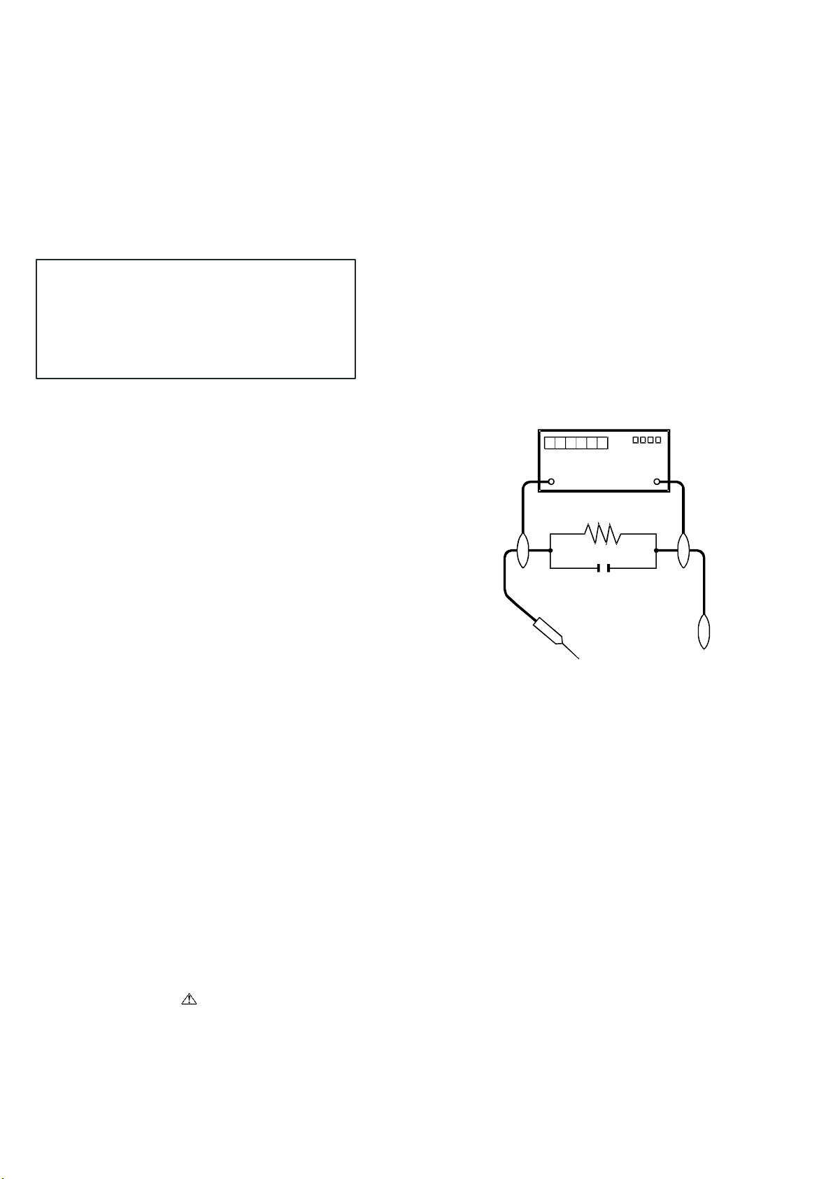
SAFETY NOTICE
Many electrical and mechanical parts in LCD color television have
special safety-related characteristics.
These characteristics are often not evident from visual inspection,
nor.
can protection afforded by them be necessarily increased by using
replacement components rated for higher voltage, wattage, etc.
Replacement parts which have these special safety characteristics
are identified in this manual; electrical components having such
features are identified by “
Replacement Parts List and Schematic Diagrams.
//////////////////////////////////////////////////////////////////////////////////////////////////////////////////////////////////////////////////////////////////////////////////////////////////////////////////////////////////////////////////
” and shaded areas in the
• Use an AC voltmeter having with 5000 ohm per volt, or higher, sen-
sitivity or measure the AC voltage drop across the resistor.
• Connect the resistor connection to all exposed metal parts having a
return to the chassis (antenna, metal cabinet, screw heads, knobs
and control shafts, escutcheon, etc.) and measure the AC voltage
drop across the resistor.
All checks must be repeated with the AC cord plug connection
reversed. (If necessary, a nonpolarized adaptor plug must be used
only for the purpose of completing these checks.)
Any reading of 1.05 V peak (this corresponds to 0.7 mA peak AC.)
or more is excessive and indicates a potential shock hazard which
must be corrected before returning the monitor to the owner.
DVM
AC SCALE
1.5k ohm
10W
0.15 µF
TEST PROBE
TO EXPOSED
METAL PARTS
CONNECT TO KNOWN
EARTH GROUND
For continued protection, replacement parts must be identical to those
used in the original circuit.
The use of a substitute replacement parts which do not have the same
safety characteristics as the factory recommended replacement parts
shown in this service manual, may create shock, fire or other hazards.
2
Page 3

LC-32LE40E-LC-42LE40E
PRECAUTIONS FOR USING LEAD-FREE SOLDER
■ Using lead-free wire solder
• When fixing the PWB soldered with the lead-free solder, apply lead-free wire solder. Repairing with conventional lead wire solder may cause damage or
accident due to cracks.
As the melting point of lead-free solder (Sn-Ag-Cu) is higher than the lead wire solder by 40 °C, we recommend you to use a dedicated soldering bit, if
you are not familiar with how to obtain lead-free wire solder or soldering bit, contact our service station or service branch in your area.
Soldering
• As the melting point of lead-free solder (Sn-Ag-Cu) is about 220 °C which is higher than the conventional lead solder by 40 °C, and as it has poor solder
wettability, you may be apt to keep the soldering bit in contact with the PWB for extended period of time. However, Since the land may be peeled off or
the maximum heat-resistance temperature of parts may be exceeded, remove the bit from the PWB as soon as you confirm the steady soldering
condition.
Lead-free solder contains more tin, and the end of the soldering bit may be easily corroded. Make sure to turn on and off the power of the bit as required.
If a different type of solder stays on the tip of the soldering bit, it is alloyed with lead-free solder. Clean the bit after every use of it.
When the tip of the soldering bit is blackened during use, file it with steel wool or fine sandpaper.
• Be careful when replacing parts with polarity indication on the PWB silk.
3
Page 4
LC-32LE40E-LC-42LE40E
CHAPTER 1. OPERATION MANUAL
[1] SPECIFICATIONS
Item
LCD screen size 32” diagonal 42” diagonal
Number of dots 3,147,264 dots (1366 x 768 x 3 dots) 6,220,800 dots (1920 x 1080 x 3 dots)
Video Colour System PAL/SECAM/NTSC 3.58/NTSC 4.43/PAL 60
32” LCD COLOUR TV
Model: LC-32LE40E
42” LCD COLOUR TV
Model: LC-42LE40E
TV-Standard
TV Function
Audio amplifier 10 W x 2 10 W x 2
Speaker 132(H) x 27(W) x 26(D) mm 132(H) x 27(W) x 26(D) mm
Rear
Receiving
Channel
TV-Tuning System Auto Preset 1599 ch, Auto Label, Auto Sort
Stereo/Bilingual NICAM/A2
ANTENNA UHF/VHF 75 Ω
RS-232C D-sub 9 pin male connector
SCART SCART (AV input, Y/C input, RGB input, TV output )
PC IN D-sub 15 pin (AV input), Ø 3.5mm jack (Audio input)
COMPONENT Y/Pb(Cb)/Pr(Cr), RCA pin (L/R)
SPDIF OUT Digital audio output
AV OUT RCA pin (AV output)
HDMI 1 Digital video and audio input, ARC
HDMI 2 Digital video and audio input
Analogue CCIR (B/G, I, D/K, L/L’)
Digital DVB-T (2K/8K OFDM), DVB-C
VHF/UHF ATV: IRA-E69, DVB-T: E5-E69
CATV S-band, S1–S41ch
C. I. (Common Interface) EN50221, R206001, CI Plus specification
Side
OSD Language
Power Requirement AC 220–240 V, 50 Hz
Power Consumption
Weight
Operating temperature 0°C to +40°C
AV IN RCA pin (AV input)
USB Software update, multi-media play
HEADPHONE Ø 3.5mm jack (Audio output)
English, German, French, Italian, Dutch, Spanish, Greek, Portuguese, Swedish,
Finnish, Russian, Polish, Turkish, Hungarian, Czech, Slovak, Danish, Norwegian,
Estonian, Latvian, Lithuanian, Slovenian, Bulgarian, Croatian, Romanian, Serbian,
Ukrainian, Gaelic, Belarussian.
59 W (Standby < 0.3W) (Method
IEC62087)
8.2 kg (Without stand), 9.4 kg (With
stand)
93 W (Standby < 0.3W) (Method
IEC62087)
12.79 kg (Without stand), 15.72 kg
(With stand)
• As a part of policy of continuous improvement, SHARP reserves the right to make design and specification changes for product improvement without
prior notice. The performance specification figures indicated are nominal values of production units. There may be some deviations from these values in
individual units.
NOTE
• Refer to the inside back cover for dimensional drawings.
• Audio cannot be output through the HDMI terminal.
4
Page 5
LC-32LE40E-LC-42LE40E
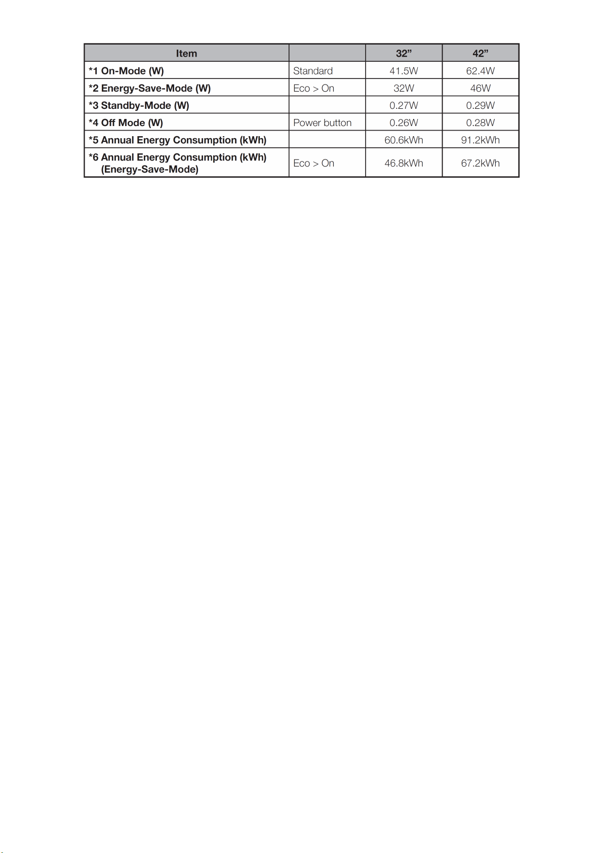
Environmental Specifications
*1 Measured according to IEC 62087 Ed. 2
*2 For further information about the Energy Save function, please see related pages in this operation manual
*3 Measured according to IEC 62301 Ed. 1
*4 Measured according to IEC 62301 Ed. 1
*5 Annual energy consumption is calculated on the basis of the On-Mode (Standard) power consumption, watching TV 4 hours a day, 365 days a year
*6 Annual energy consumption is calculated on the basis of the Energy-Save-Mode power consumption, watching TV 4 hours a day, 365 days a year.
NOTE
• The power consumption of On-Mode varies depending on the images the TV displays.
5
Page 6
LC-32LE40E-LC-42LE40E
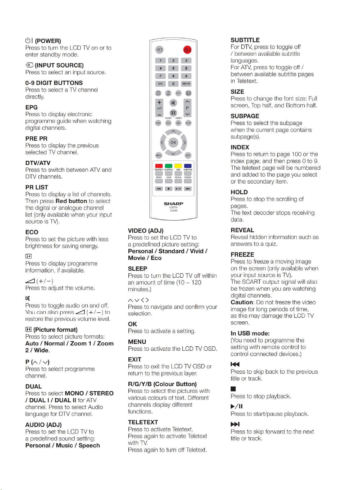
[2] OPERATION MANUAL
Remote Control
6
Page 7
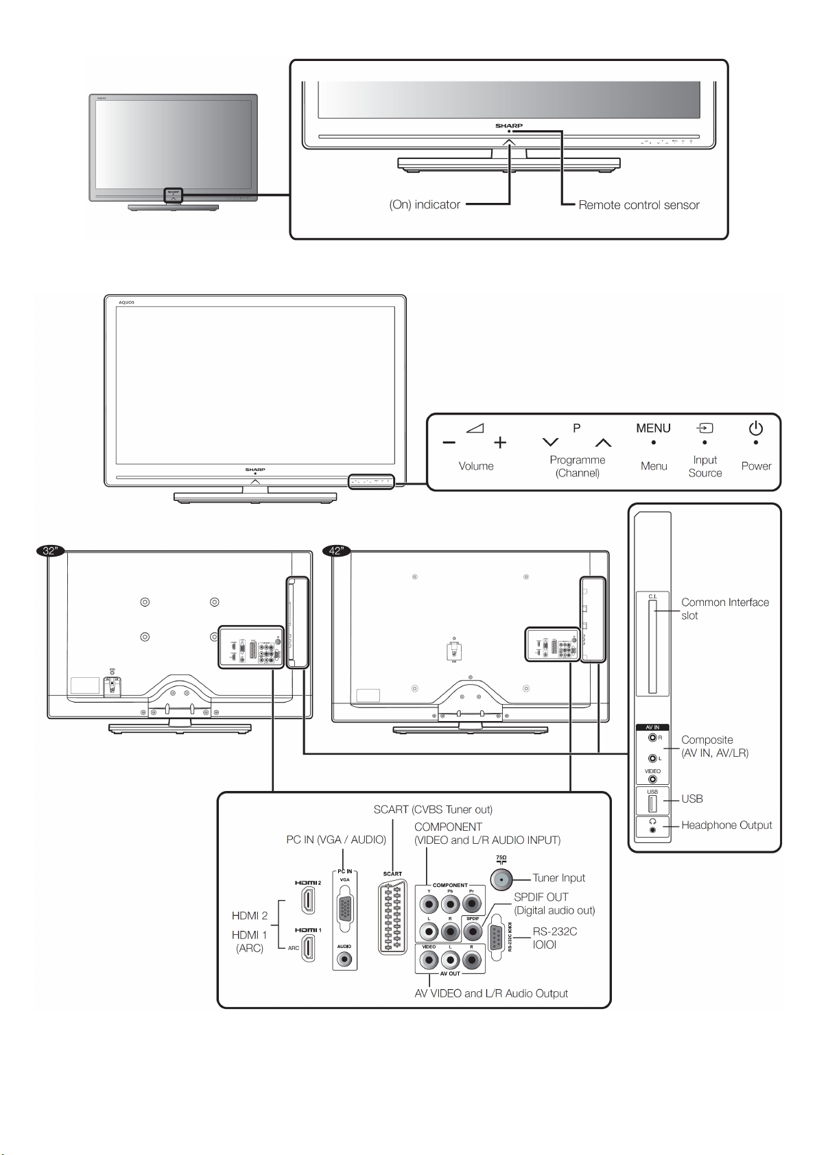
TV (Front)
TV (Side/Rear)
LC-32LE40E-LC-42LE40E
7
Page 8
LC-32LE40E-LC-42LE40E
Preparation
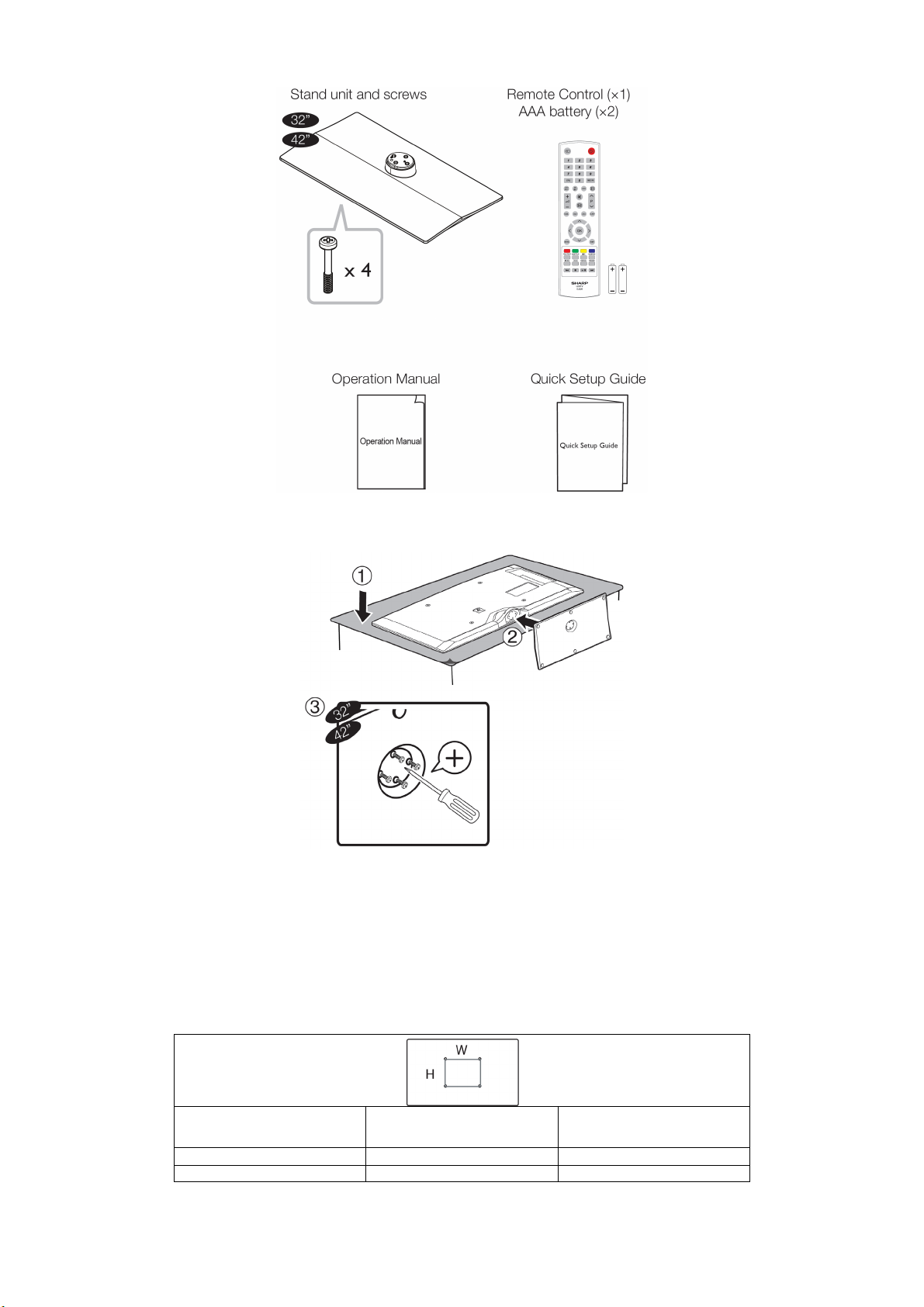
Supplied Accessories
Mount the TV base
1. Put the TV with its face down on a safe surface covered by a soft and smooth cloth. 2. Adjust the TV base to the bottom of the TV. Please be sure the
arrow heads are facing front.
3. Fasten the screws by using a cross-head screwdriver (not supplied).
NOTE
• To detach the TV stand, do these steps in reverse order.
Wall Mounting
TV screen size
32” 200 x 100 mm 4 x 10 mm
42” 400 x 400 mm 4 x 10 mm
Note
• At the time of purchasing wall bracket, please check if there is enough space between the wall bracket and TV terminals for the terminal connection
VESA-compatible wall bracket
(W x H)
Screw type (Metric)
8
Page 9
LC-32LE40E-LC-42LE40E
Preparation
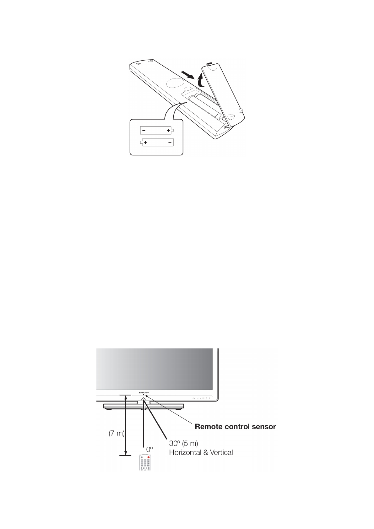
Installing Batteries in the Remote Control Unit
1 Insert two AAA batteries into remote control. Make sure the (k) and (l) ends are facing correct direction.
2 Replace the cover.
NOTE
• If you are not going to use the remote control for a long time, remove the batteries to avoid damaging remote control caused by chemical leakage.
CAUTION
Improper use of batteries can result in chemical leakage or explosion. Be sure to follow the instructions below:
• Do not mix batteries of different types. Different types of batteries have different characteristics.
• Do not mix old and new batteries. Mixing old and new batteries can shorten the life of new batteries or cause chemical leakage in old batteries.
• Remove batteries as soon as they have worn out. Chemicals that leak from batteries can cause a rash. If you find any chemical leakage, wipe thoroughly
with a cloth.
• The batteries supplied with this product may have a shorter life expectancy due to storage conditions.
Note on disposing batteries:
The batteries provided contain no harmful materials such as cadmium, lead or mercury.
Regulations concerning used batteries stipulate that batteries may no longer be thrown out with the household rubbish. Deposit any used batteries free of
charge into the designated collection containers set up at commercial businesses.
Using the Remote Control Unit
Use the remote control unit by pointing it towards the remote control sensor. Objects between the remote control unit and sensor may block proper
operation.
9
Page 10
LC-32LE40E-LC-42LE40E
Appendix
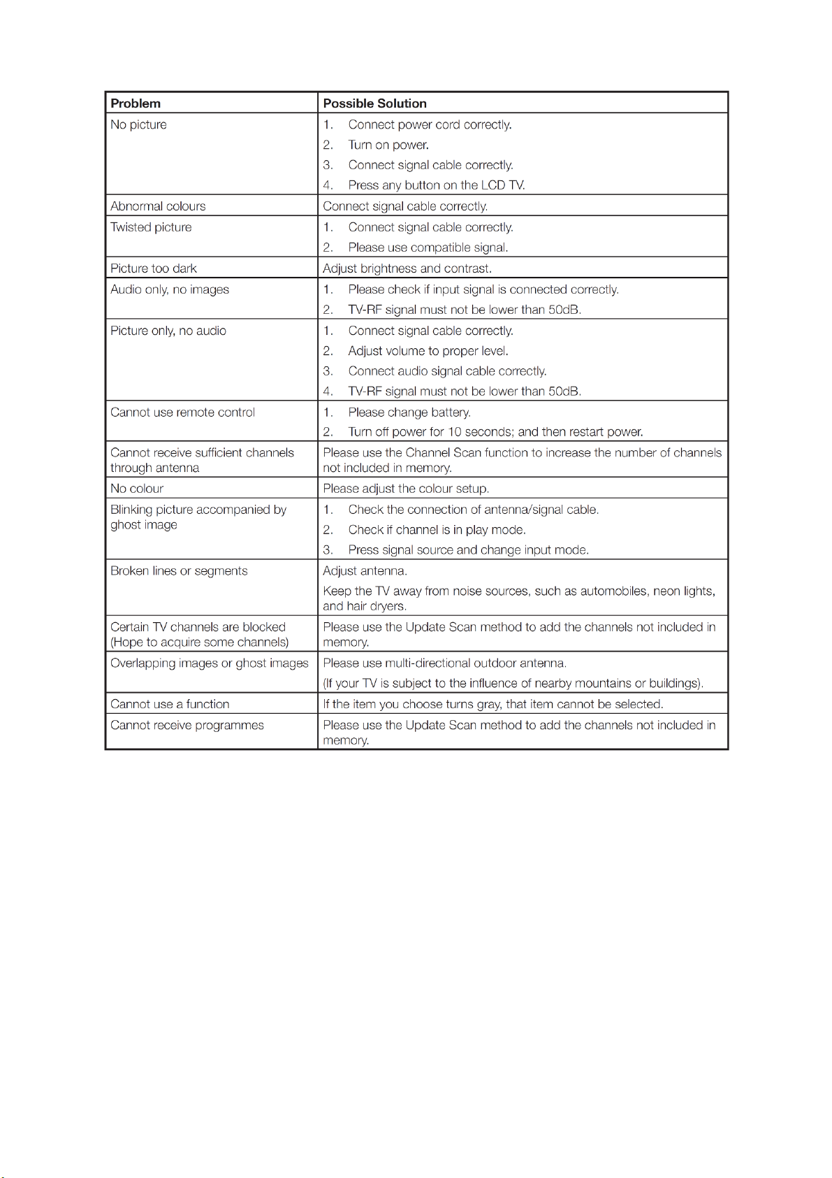
Troubleshooting
Information on the Software License for This Product
Software composition
The software included in this product is comprised of various software components whose individual copyrights are held by SHARP or by third parties.
Software developed by SHARP and open source software
The copyrights for the software components and various relevant documents included with this product that were developed or written by SHARP are
owned by SHARP and are protected by the Copyright Act, international treaties, and other relevant laws. This product also makes use of freely
distributed software and software components whose copyrights are held by third parties. These include software components covered by a GNU
General Public License (hereafter GPL), a GNU Lesser General Public License (hereafter LGPL) or other license agreement.
Acknowledgements
The following open source software components are included in this product:
Linux kernel/Modutils/Glibc/Zlib/Libpng
10
Page 11
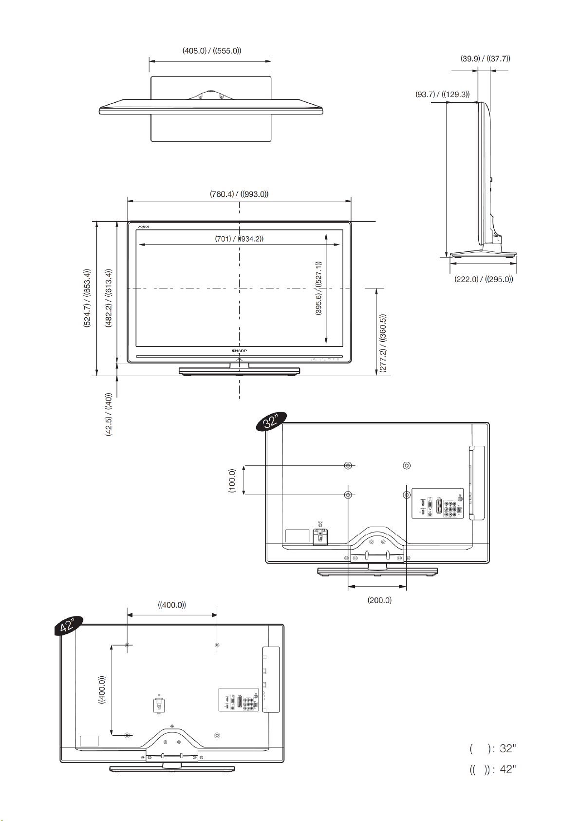
[3] DIMENSIONS
LC-32LE40E-LC-42LE40E
11
Page 12
LC-32LE40E-LC-42LE40E
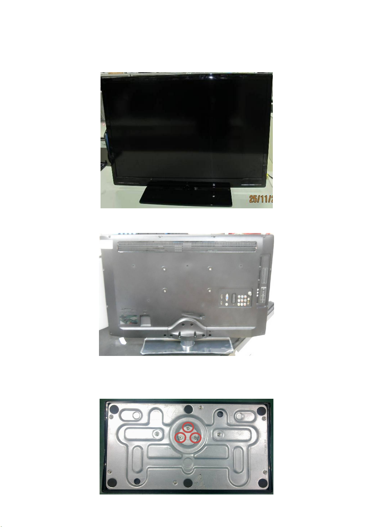
CHAPTER 2. REMOVING OF MAJOR PARTS
[1] ASSY/PANEL REMOVAL
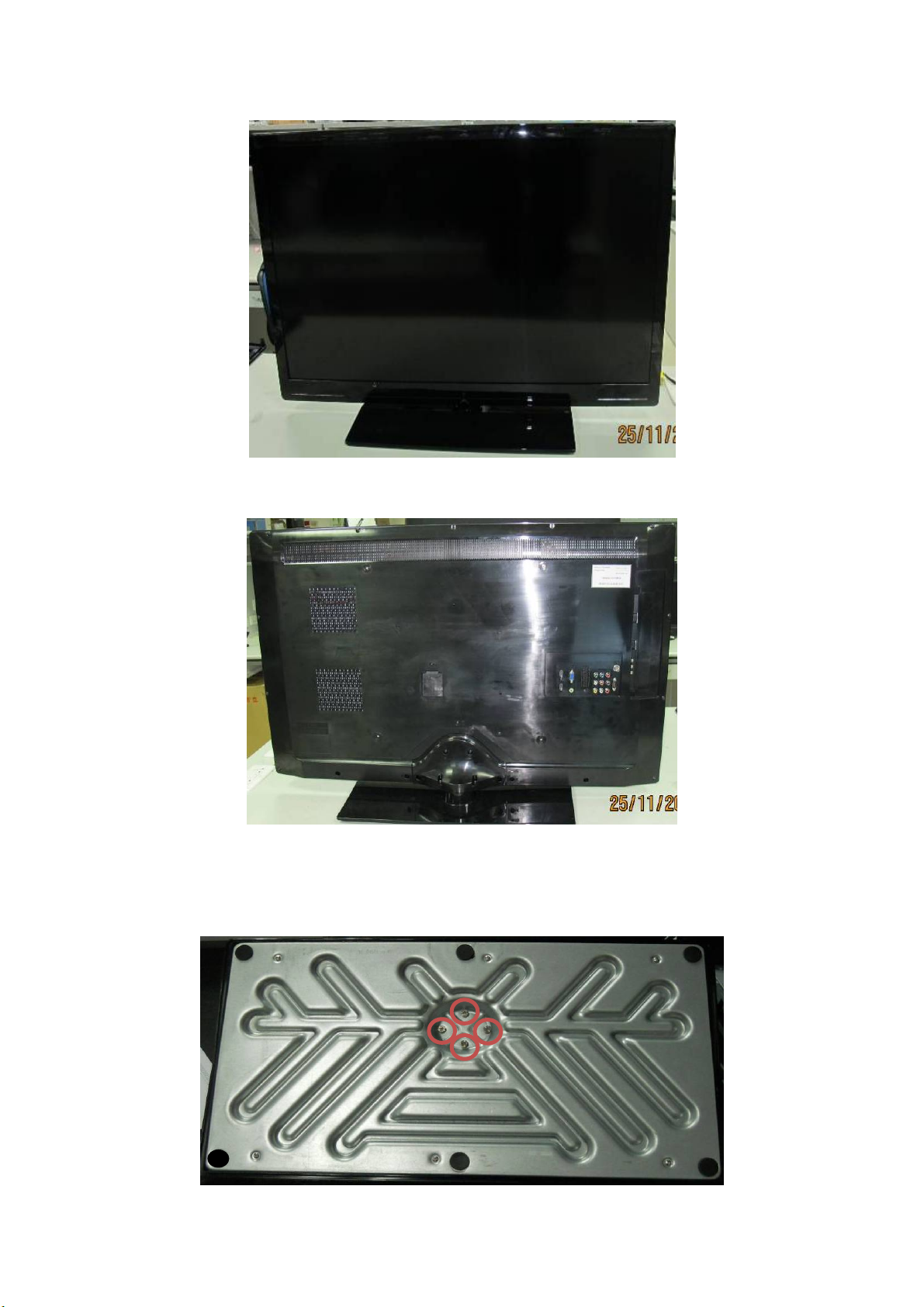
LC-32LE40E
Note: Put the TV face down on a safe surface that is covered by a soft and smooth cloth to avoid damaging LCD Panel.
Front View
Back View
Step 1. Remove the base.
A. Remove 3 screws as fig 3 and put out the base.
Fig 1
Fig 2
Fig 3
12
Page 13
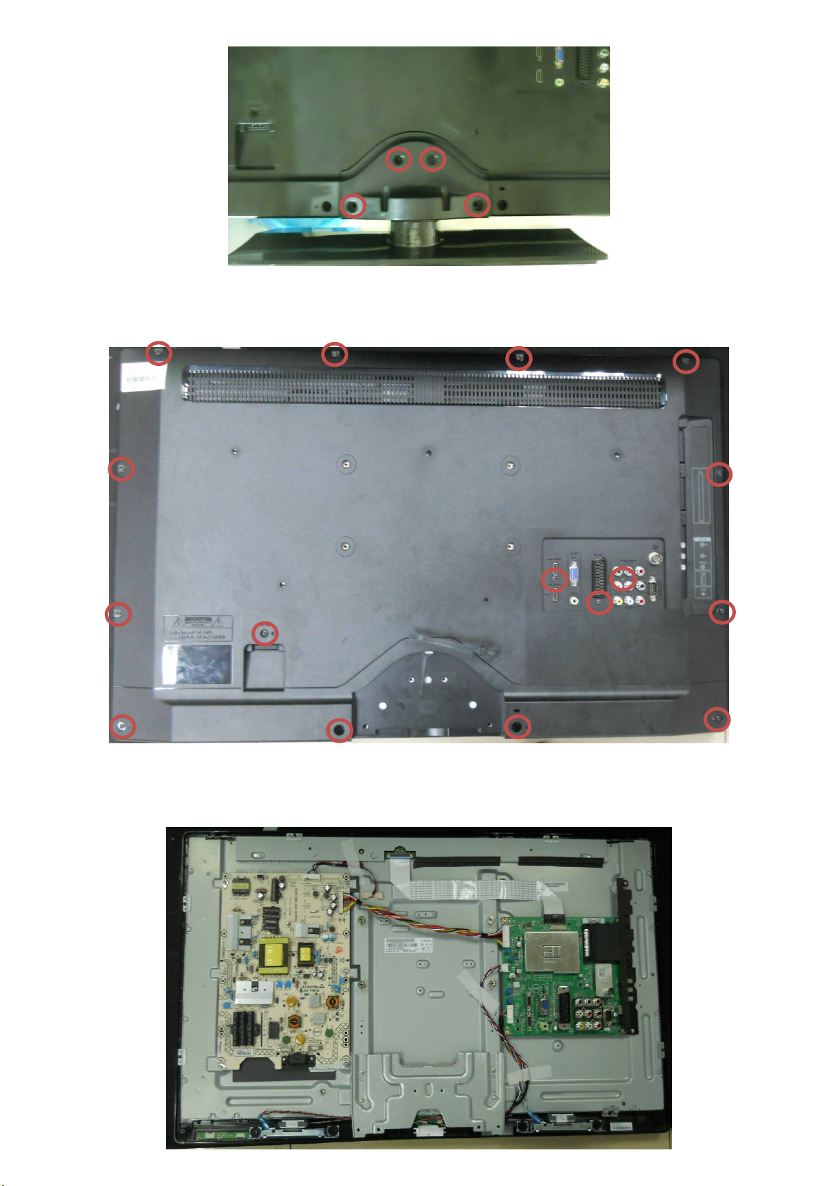
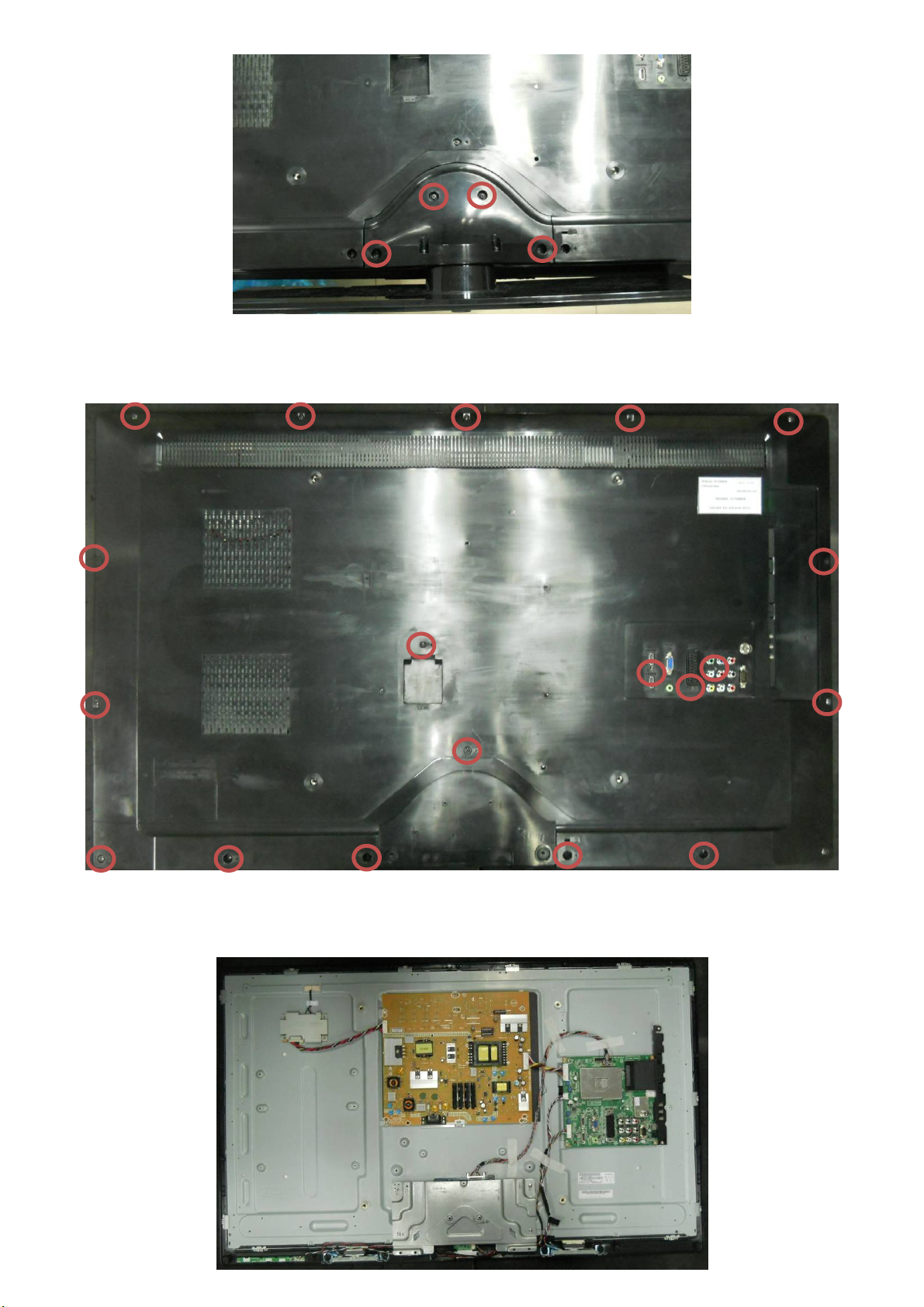
B. Remove 4 screws as Fig 4 to detach the stand.
LC-32LE40E-LC-42LE40E
Step 2. Remove the rear cover.
Remove 16 screws as Fig 5
Fig 4
Step 3. Remove the bkt_stand.
Remove 4 screws as Fig 6
Fig 5
13
Page 14
LC-32LE40E-LC-42LE40E
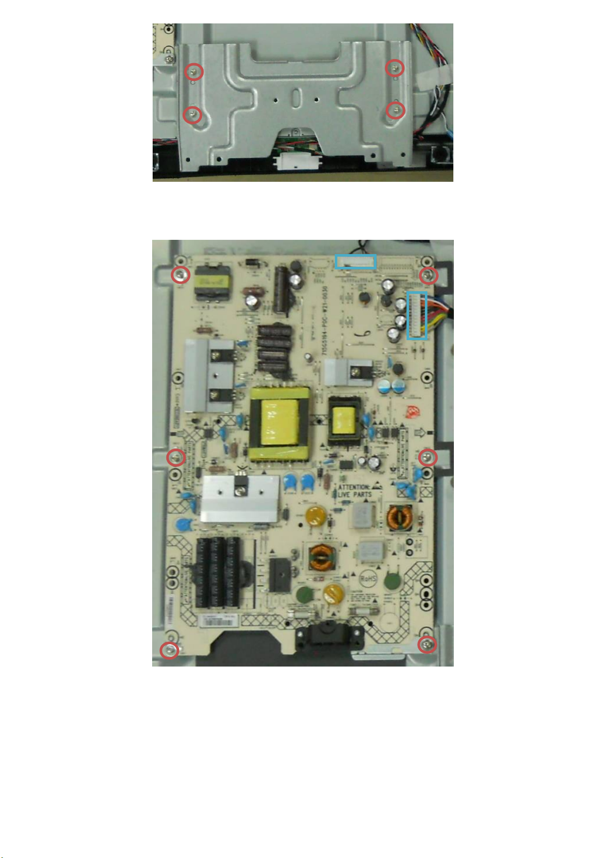
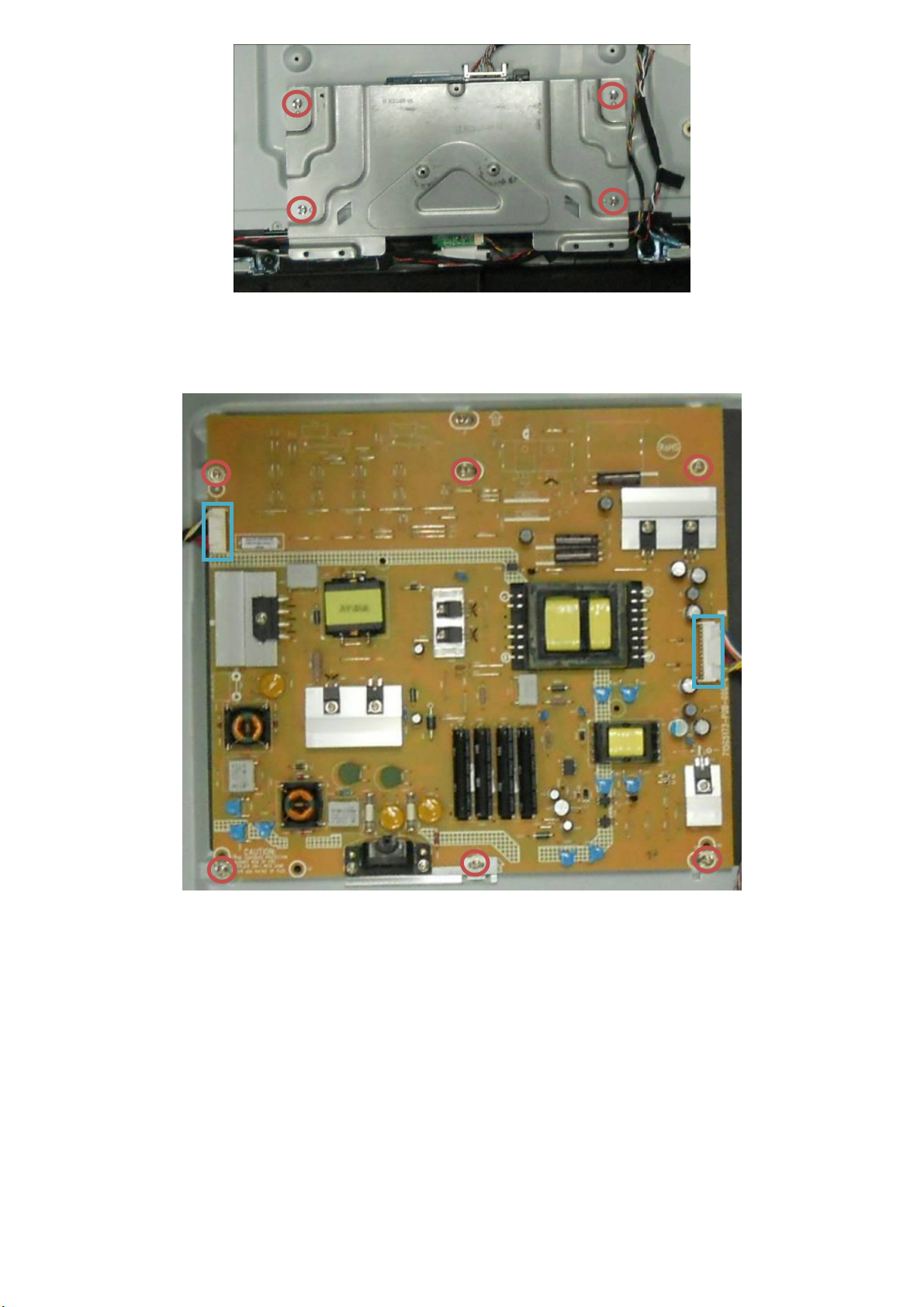
Step 4. Remove the power board.
Remove 6 screws and unplug 2 cables as Fig 7
Fig 6
Fig 7
14
Page 15
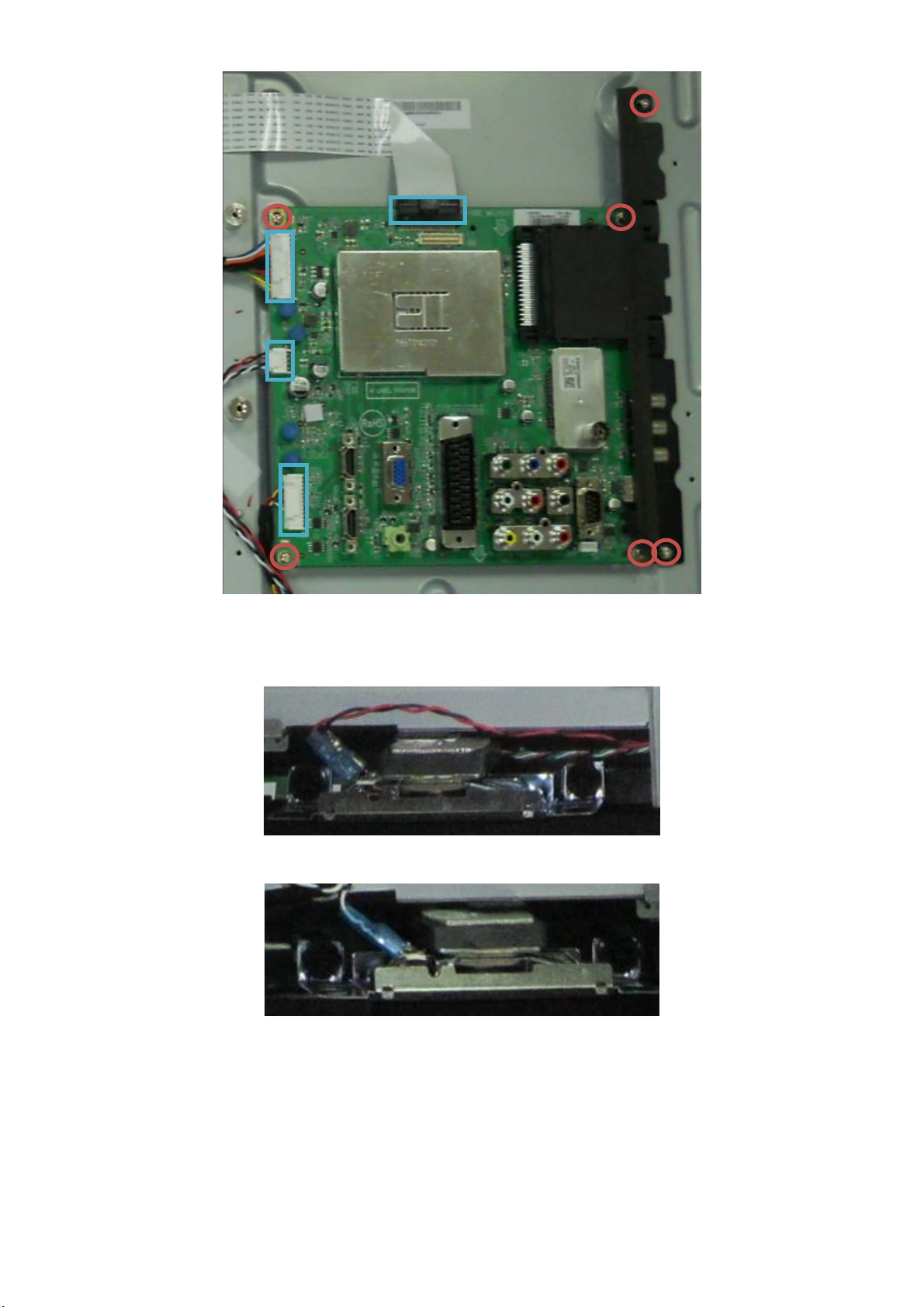
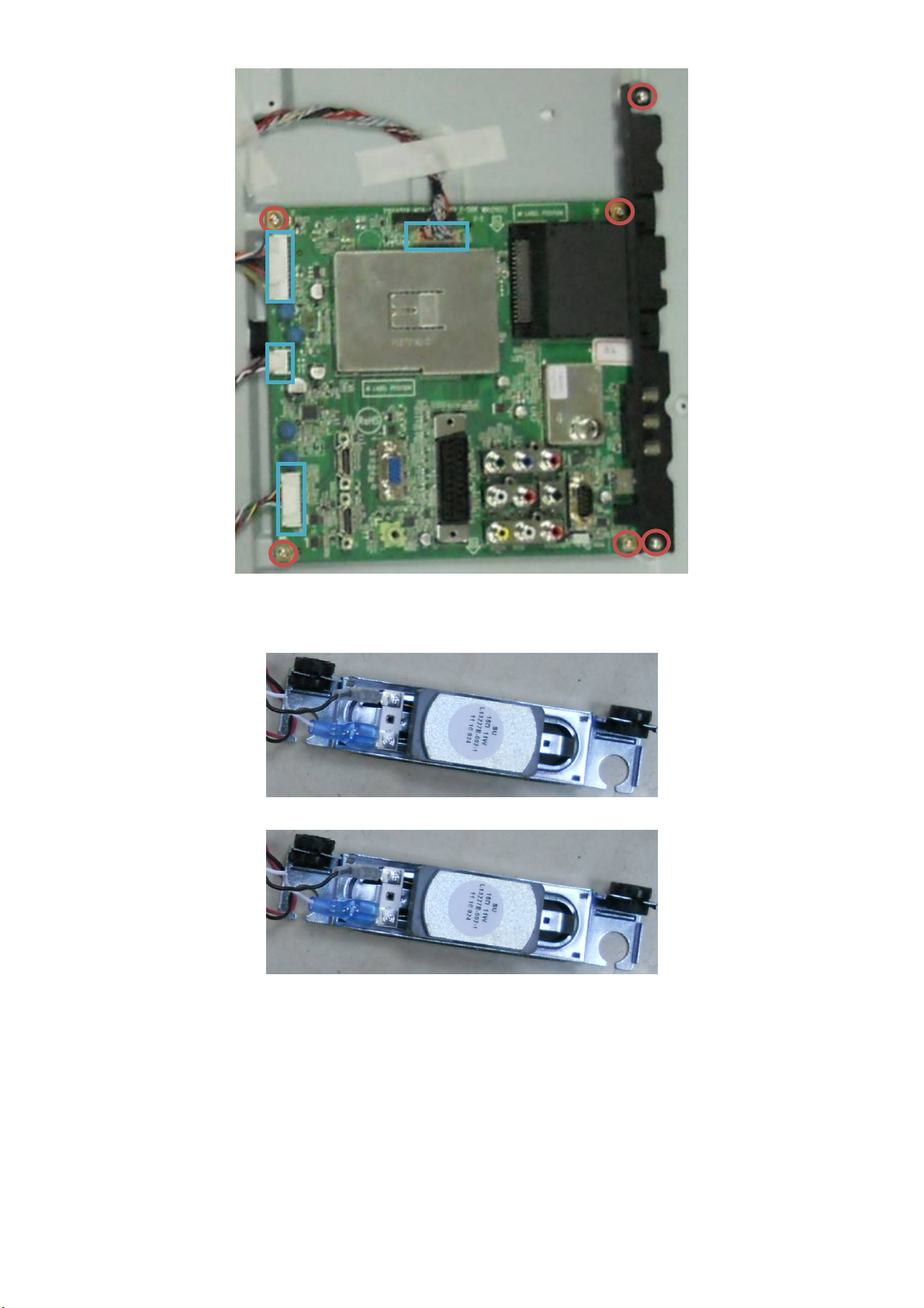
Step 5. Remove the scaler board.
Remove 6 screws and unplug 4 cables as Fig 8
LC-32LE40E-LC-42LE40E
Step 6. Remove the speakers(L/R).
Remove as Fig 9 and Fig 10
Fig 8
Fig 9
Fig 10
15
Page 16
LC-32LE40E-LC-42LE40E
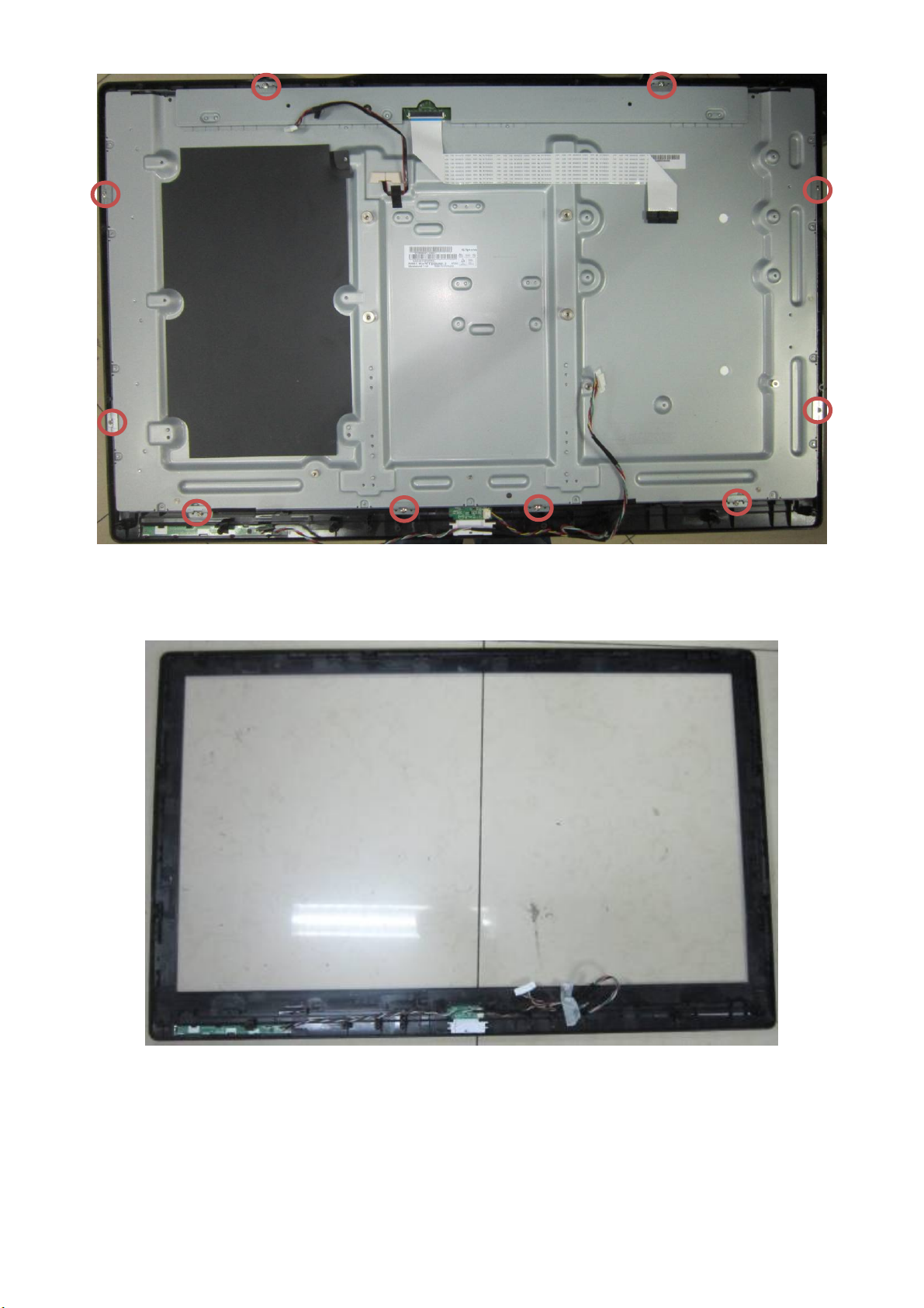
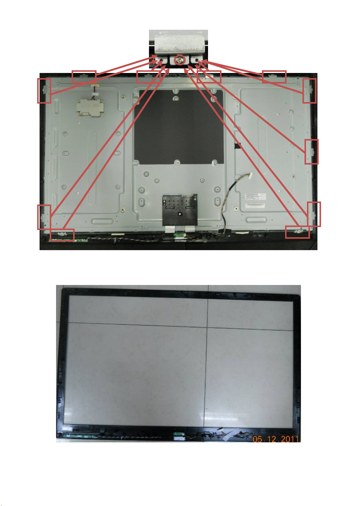
Step 7. Remove the bkt_panel and separate the panel and bezel.
Remove 10 screws as Fig 11
Step 8. Bezel assy.
The bezel assy as Fig 12
Fig 11
Fig 12
16
Page 17
LC-42LE40E
Note: Put the TV face down on a safe surface that is covered by a soft and smooth cloth to avoid damaging LCD Panel.
Front View
Fig 1
LC-32LE40E-LC-42LE40E
Back View
Step 1. Remove the base.
A. Remove 4 screws as fig 3 and put out the base.
Fig 2
Fig 3
17
Page 18
LC-32LE40E-LC-42LE40E
B. Remove 4 screws as Fig 4 to detach the stand.
Step 2. Remove the rear cover.
Remove 19 screws as Fig 5
Fig 4
Step 3. Remove the bkt_stand.
Remove 4 screws as Fig 6
Fig 5
18
Page 19
Step 4. Remove the power board.
Remove 6 screws and unplug 2 cables as Fig 7
LC-32LE40E-LC-42LE40E
Fig 6
Fig 7
19
Page 20
LC-32LE40E-LC-42LE40E
Step 5. Remove the scaler board.
Remove 6 screws and unplug 4 cables as Fig 8
Step 6. Remove the speakers(L/R).
Remove as Fig 9 and Fig 10
Fig 8
Fig 9
Fig 10
20
Page 21
Step 7. Remove the bkt_panel and separate the panel and bezel.
Remove 11 screws as Fig 11
LC-32LE40E-LC-42LE40E
Step 8. Bezel assy.
The bezel assy as Fig 12
Fig 11
Fig 12
21
Page 22

LC-32LE40E-LC-42LE40E
[2] SET RE-ASSEMBLY
To re-assemble the whole set, execute all processes in reverse order.
Note
a. While re-assembling, make sure that all cables are placed and connected in their original position.
b. Pay special attention not to damage the EMC foams at the SSB shielding. Check that EMC foams are put correctly on their places.
22
Page 23
CHAPTER 3. ADJUSTMENT PROCEDURE
[1] ADJUSTMENT PROCEDURE
1. OSD Menu
OSD tree - As following
Sharp DVB OSD tree-Video
OSD Layer 1 2 3 4 5 6 Note
Personal All
Standard All
Picture
Sound
Smart Picture
Brightness slider All
Contrast slider All
Color slider All
Tint slider All
Sharpness slider All
Color Temperature
Advanced
Control(have sub
page)
Sound Mode
Equilizer 120Hz slider All
Equilizer 500Hz slider All
Equilizer 1.5KHz slider All
Equilizer 5KHz slider All
Equilizer 10KHz slider All
Balance slider All
Virtual Surround
Digital Audio Out
(If source is HDMI.
This function will
be disable )
AVL
Type(if source is Normal All
Vivid All
Movie All
Eco All
Normal (default) All
Cool All
Warm All
Off All
Low All
Noise Reduction
Flesh Tone
Back Light(if DCR is
Off)
DCR
C.M.S.-value
Advanced (Only for
32"37"42"LE320
100Hz model)
Personal All
Music All
Speech All
On All
Off All
PCM All
Off All
Dolby Digital All
Off All
On All
Medium All
HIGH All
Auto All
On All
Off All
slider All
On All
Off All
Mode 100Hz All
Film Mode All
Effect Off All
Low All
Middle All
High All
LC-32LE40E-LC-42LE40E
Model
Number
23
Page 24
LC-32LE40E-LC-42LE40E
DTV)
Audio
Description(if
Type=Audio
Description)
Tuner Mode
Country(31)
TV
Hard of Hearing All
Audio Description All
Volume slider
Antenna All
Cable All
UK All
Italy All
Luxembourg All
Netherlands All
Norway All
Sweden All
Croatia All
Hungary All
Ireland All
Poland All
Portugal All
Romania All
Serbia All
Slovakia All
Slovenia All
Turkey All
Iceland All
Russia All
Ukraine All
Austria All
Belgium All
Bulgaria All
Switzerland All
All
All
All
Czech Republic All
Germany All
Greece All
Denmark All
Spain All
Finland All
France All
Other All
English All
Finnish All
French All
Gaelic All
Galician All
German All
1st Audio(28)(DTV
only)
Greek All
Hungarian All
Italian All
Norwegian All
Polish All
Portuguese All
Romanian All
Russian All
Serbian All
24
Page 25
2nd
Audio(28)(DTV
only)
Channels(have
sub page)
LC-32LE40E-LC-42LE40E
Slovak All
Slovenian All
Spanish All
Swedish All
Turkish All
Welsh All
Basque All
Bulgarian All
Catalan All
Croatian All
Czech All
Danish All
Dutch All
English All
Finnish All
French All
Gaelic All
Galician All
German All
Greek All
Hungarian All
Italian All
Norwegian All
Polish All
Portuguese All
Romanian All
Russian All
Serbian All
Slovak All
Slovenian All
Spanish All
Swedish All
Turkish All
Welsh All
Basque All
Bulgarian All
Catalan All
Croatian All
Czech All
Danish All
Dutch All
Channel Scan
ATV
ATV and
DTV( if
Antenna
mode)
ATV and
DTV( if Cable
mode)
Status:
scanning…
Analogue
channels:
Status:
scanning…
Analogue
channels:
Digital
channels:
Scan Mode
All
All
All
All
All
Full/Quick/Adv
anced
(There is
Quick
selection if
country is
selected
Geremy,Finlan
d,Norway)
All
25
(if Advance
mode select)
Frequency(KH
z)
All
Page 26
LC-32LE40E-LC-42LE40E
Update Scan( Only
available for
Antenna mode)
Single RF Scan( if
Antenna mode)
Single RF Scan( if
Cable mode)
Analog Manual Scan
Modulation
Network ID All
Scan
Status:
scanning…
Analogue
channels:
Digital
channels:
RF Channel .. slider All
Signal
Strength..
Signal
Quailty..
Frequency(KH
z)
Modulation
=>Auto/16/32/
64/128/256
QAM
Symbol
Rate(Ksym/s)
Signal
Strength..
Start
Frequency
Scan Up All
Scan Down All
All
All
All
All
All
slider All
All
All
All
xxMHz All
=>Auto/16/32/
64/128/256
QAM
Symbol
Rate(Ksym/s)
Status:
scanning…
Analogue
channels:
Digital
channels:
All
All
All
All
All
Features
Menu
Language(29)
Favorite Network
Select
Channel Skip(have
sub page)
Channel Sort
Channel Move(have
sub page)
Channel Edit(have
sub page)
Decoder(for ATV)
Analog Ch Fine
Tune
Clean Channel List All
English All
Deutsch All
Français All
Italiano All
Español All
Português All
Nederlands All
Български All
Dansk All
Suomi All
Svenska All
Norsk All
Polski All
Русский All
All
(Channel
munber…)
Numerical
Order
Aplphabetical
Order
(Channel
munber…)
(Channel
munber…)
(Channel
munber…)
(Channel
munber…)
(have sub
page)
All
All
All
All
(do fine
tune)
All
26
Page 27
LC-32LE40E-LC-42LE40E
Česky All
Hrvatski All
Magyar All
Română All
Slovenský All
Slovenščina All
Srpski All
Türkçe All
Ελληνικά All
Gaeilge All
Latviski All
Eesti All
Lietuviskai All
ykpaiHcbka All
Byelorussian All
4:3 mode
Picture Format(if
video exist)
Time (have sub
page )
4:3 All
16:9 All
Auto All
Normal All
Zoom1 All
Zoom2 All
Wide All
Time Zone
As
Broadcaster
GMT +0:00 All
GMT +1:00 All
GMT +2:00 All
GMT +3:00 All
GMT +3:30 All
GMT +4:00 All
GMT +4:30 All
GMT +5:00 All
GMT +5:30 All
GMT +5:45 All
GMT +6:00 All
GMT +6:30 All
GMT +7:00 All
GMT +8:00 All
GMT +9:00 All
GMT +9:30 All
GMT +10:00 All
GMT +11:00 All
GMT +12:00 All
GMT +12:45 All
GMT +13:00 All
GMT -12:00 All
GMT -11:00 All
GMT -10:00 All
GMT -9:00 All
GMT -8:00 All
GMT -7:00 All
GMT -6:00 All
GMT -5:00 All
GMT -4:00 All
GMT -3:30 All
GMT -3:00 All
All
27
Page 28
LC-32LE40E-LC-42LE40E
SCART(have sub
page)
(Only availabe in
SCART source)
Input label
Subtitle(have sub
page)
Time(have sub
page)
Sleep Timer
SCART1
SCART2(If have I/O)
Analog Subtitle
1st Subtitle(28)
GMT -2:00 All
GMT -1:00 All
Auto
synchronizatio
n ( On/Off)
Date
( 20xx/xx/xx )
Time
( xx:xx:xx)
Timer (Off/On) All
Off Time
( xx:xx:xx)
Off All
10 Min All
20 Min All
30 Min All
40 Min All
50 Min All
60 Min All
90 Min All
120 Min All
Auto All
Mixed All
RGB All
Composite All
S-Video All
Auto All
Composite All
S-Video All
On All
On during
mute
Off All
English All
Finnish All
French All
Gaelic All
Galician All
German All
Greek All
Hungarian All
Italian All
Norwegian All
Polish All
Portuguese All
Romanian All
Russian All
Serbian All
Slovak All
Slovenian All
Spanish All
Swedish All
Turkish All
Welsh All
Off All
Basque All
Bulgarian All
Catalan All
All
All
All
All
All
28
Page 29
Teletext
Language(have
sub page)
2nd Subtitle(28)
Subtitle Type
Digital Teletext
Lang.
LC-32LE40E-LC-42LE40E
Croatian All
Czech All
Danish All
Dutch All
English All
Finnish All
French All
Gaelic All
Galician All
German All
Greek All
Hungarian All
Italian All
Norwegian All
Polish All
Portuguese All
Romanian All
Russian All
Serbian All
Slovak All
Slovenian All
Spanish All
Swedish All
Turkish All
Welsh All
Off All
Basque All
Bulgarian All
Catalan All
Croatian All
Czech All
Danish All
Dutch All
Normal All
Hearing
Impaired
English All
Finnish All
French All
Gaelic All
Galician All
German All
Greek All
Hungarian All
Italian All
Norwegian All
Polish All
Portuguese All
Romanian All
Russian All
Serbian All
Slovak All
Slovenian All
Spanish All
Swedish All
Turkish All
Welsh All
All
29
Page 30
LC-32LE40E-LC-42LE40E
CEC Setup
Common
Interface(have sub
page)
HDMI Scan Info
(Only available in
HDMI source)
Basque All
Bulgarian All
Catalan All
Croatian All
Czech All
Danish All
Dutch All
WEST EUR All
EAST EUR All
Russia All
Russia-2 All
Decode Page Lang.
Enable CEC
Auto Power On
Auto Standby
Amplifier Control
Speaker Preference
(display some info &
status..)
Automatic All
Underscan All
Overscan All
Manual OAD
Download
Greek All
Turkey All
Arab/Hbrw All
Farsian All
Arab All
BYELORUSSI
AN
On All
Off All
On All
Off All
On All
Off All
On All
Off All
TV speaker All
Amplifier All
All
Scanning… (if
has oad
information.)
All
All
Auto Download (only
country setting is
Norway)
OAD
No All
Auto Install (only
country setting is
Norway)
No All
No Signal Off
No Operation Off
Reset Default All
Demo
DivX(R)
Registration
DivX(R)
Deactivation
On
Off
On
Off
Top All
Bottom
Off
All
Yes All
Yes All
All(HT
3.0 or
HD 1.1)
30
Page 31

Parental
LC-32LE40E-LC-42LE40E
SW Ver. All
Channel Block(have
sub page)
Time Interval Lock
(Only available for
country is selected
"Norway")
Password(have
sub page)
Parental
Guidance(have sub
page)
(Channel
munber…)
Lock Type
Start Time ( xx:xx:xx) All
End Time ( xx:xx:xx) All
Age Rating
All
None All
Everyday All
Sunday All
Monday All
Tuesday All
Wednesday All
Thursday All
Friday All
Saturday All
18 All
None All
4 All
5 All
6 All
7 All
8 All
9 All
10 All
11 All
12 All
13 All
14 All
15 All
16 All
17 All
Input Block(have
sub page)
Set password (have
sub page)
Clear All All
Eco
On / Off (← toggle
selection)
All
(Source list..)
(TV,YPbPr,AV
,SCART,PC,H
DMI)
New
Password
(xxxx)
Confirm
Password
(xxxx)
All
All
All
31
Page 32

LC-32LE40E-LC-42LE40E
Sharp DVB OSD tree--PC
OSD Layer 1 2 3 4 5 6 Note
Brightness slider All
Contrast slider All
Normal (default) All
Picture
Sound
Features
Color Temperature
Advanced
Video(have sub
page)
Sound Mode
Equilizer 120Hz slider All
Equilizer 500Hz slider All
Equilizer 1.5KHz slider All
Equilizer 5KHz slider All
Equilizer 10KHz slider All
Balance slider All
Virtual Surround
Digital Audio Out
Menu Language(29)
Picture Format
Input label
No Signal Off
Cool All
Warm All
Auto Config Auto Config All
Horizontal slider All
Vertical slider All
Phase slider All
Clock slider All
Resolution(if
ambiguous timings)
Personal All
Music All
Speech All
On All
Off All
PCM All
Off All
Dolby Digital All
English All
Deutsch All
Français All
Italiano All
Español All
Português All
Nederlands All
Български All
Dansk All
Suomi All
Svenska All
Norsk All
Polski All
Русский All
Česky All
Hrvatski All
Magyar All
Română All
Slovenský All
Slovenščina All
Srpski All
Türkçe All
Ελληνικά All
Gaeilge All
Latviski All
Eesti All
Lietuviskai All
ykpaiHcbka All
Byelorussian All
Full screen All
Native ( if is native
timing)
4:3 All
On
Off
1360*768 All
1024*768 All
1280*768 All
All
32
Model
Number
Page 33

Parental
LC-32LE40E-LC-42LE40E
No Operation Off
Reset Default All
Demo
DivX(R) Registration All
DivX(R) Deactivation
SW Ver. All
Password(have sub
page)
On
Off
Top All
Bottom
Off
All(HT
3.0 or
HD 1.1)
None All
Everyday All
Sunday All
Time Interval Lock
(Only available for
country is selected
"Norway")
Parental
Guidance(have sub
page)
Lock Type
Start Time ( xx:xx:xx) All
End Time ( xx:xx:xx) All
Age Rating
Monday All
Tuesday All
Wednesday All
Thursday All
Friday All
Saturday All
18 All
None All
4 All
5 All
6 All
7 All
8 All
9 All
10 All
11 All
12 All
13 All
14 All
15 All
16 All
17 All
Input Block(have
sub page)
Set password (have
sub page)
Clear All All
Eco
On / Off (← toggle
selection)
All
(Source list..)
(TV,YPbPr,AV,SCART,PC,HDMI)
New Password (xxxx) All
Confirm Password (xxxx) All
All
33
Page 34

LC-32LE40E-LC-42LE40E
2. ADC Adjustment and White Balance Adjustment
This sop only meet below TV mode.
Sharp LC-32LE40E
Sharp LC-42LE40E
Introduction of adjust item:
It only need adjust WB( Ypbpr/VGA
Content of WB Adjustment
1. Enter into the factory mode:(same as the above-mentioned).
2.Take an example of adjust Ypbpr_Normal:
a.Select item “Source”: Ypbpr
b.Adjust gain of RGB to meet spec in the below setting of tim\pat.
(COMPONENT mode: TIM = 314; PAT = 141(80IRE))
3. Take an example of adjust VGA_Normal:
’s Normal/Warm/Cool ).
and item “Color Temp”: Normal .
a.Select item “Source”: VGA
b.Adjust gain of RGB to meet spec in the below setting of tim\pat.
(VGA mode: TIM = 137; PAT = 141(80IRE))
and item “Color Temp”: Normal .
Normal/ (7500 K) Warm/ (6500K) Cool / (9300K)
x (center) 0.289 0.015 0.314 0.015 0.272 0.015
y (center) 0.291 0.015 0.319 0.015 0.277 0.015
Lv(center) >300cd >300cd >300cd
34
Page 35

[2] SOFTWARE UPGRADE PROCEDURE
FW Upgrade
Step 1: Ready for F/W Upgrade (Only for client user)
1.1 Change the software file name to “upgrade.pkg”, eg:
LC-32LE40E-LC-42LE40E
After change:
1.2 Prepare a USB disk (The file system of USB disk must be FAT16 or FAT 32).
1.3 Copy the file (upgrade.pkg) from your computer to the USB disk root directory, and remove it from computer’s USB port!
Note:
1). Note the version of this F/W before you change the software file name.
2). The software file name must be changed, or TV can’t detect the F/W.
Step 2: F/W Upgrade
2.1 AC on (Power plug)
2.2 Plug the USB disk on the USB port on the side I/O port of TV.
2.3 TV AC power off -> AC power on
2.4 TV will upgrade after detect the USB disk condition and the content of the pkg file,press Yes to upgrade. then select Next to start upgrade the
firmware.
35
Page 36

LC-32LE40E-LC-42LE40E
2.5 Remove USB disk from TV.
2.6 Check if the software version is correct.
Press “MENU+1999+PRE PR”, enter factory mode.
2.7 Please do factory reset, select reset then press .
2.8 Reset finish, AC OFF.
36
Page 37

The Writing EDID
Take LC-32LE40E for example
1. Materials list
ISP JIG: 715GT080- A VGA cable PC
LC-32LE40E-LC-42LE40E
Monitor USB cable Tool New F/W
2. Connection
Connect to PC
USB port by USB
cable.
TPV P/N: 089G1758 X
Connect to TV
VGA port by
VGA cable.
3. FW upgrade
1. It needs following file to run RW_EEPROM_by_FactoryCommand program:
1. RW_EEPROM_by_FactoryCommand.exe Program
2. RW_EEPROM_by_FactoryCommand.ini Config saved file
37
Page 38

LC-32LE40E-LC-42LE40E
3. FactoryCommand.ini Enter factory mode command
2. After run the program, RW_EEPROM_by_FactoryCommand, it will show below:
3. Select COM port:
Select COM port number in combobox, you can press “Port” button to test whether Com port is available or not.Then press open.
4. Select EEPROM.
Select 24C128.
When read or write data , it’s current
processing address
Com port and baud rate
Yellow color means port is close
Green color means port open
38
Page 39

5. Enter factory mode:
Press this button to enter factory mode and enable following 5 buttons:
LC-32LE40E-LC-42LE40E
6. Read from BIN file:
It will show a file browser dialog to select BIN file
After reading all data, it will calculate CheckSum on left-bottom cornor.
7. Write to EEPROM:
Write all data to EEPROM, if all data are ready (no empty cells).
Program will write 8 bytes, and then read 8 bytes back for confirmation until finishes working..
39
Page 40

LC-32LE40E-LC-42LE40E
40
Page 41

CHAPTER 4. TROUBLESHOOTING TABLE
p
[1] TROUBLESHOOTING TABLE
Power unit operation check.
↓
Are the power cord and harness in the unit properly connected?
LINE_FILTER_UNIT: ↓ YES
Is F9901/F9902 normal?
POWER_UNIT
Is B+_main(32”)/B1+(42”) output? (Set the main power SW to ON.)
↓YES
↓YES
Is a voltage of +5.2V applied to pin (2,3) of connector
(CN9304(32”)/CN907(42”))?
(Set the main power SW to ON.)
↓YES
Are 12 and 24V output as for the power on/off switch when it is on?
The sound is not emitted from the speaker though the picture has come out.
↓
No sound output in all modes?
TERMINAL UNIT: ↓
Is the audio signal output of IC U401 normal?
↓YES
Is audio signal input to pin (15/20/21/22) of IC U602 (AMP)?
↓YES
Is MUTE circuit [AMP_MUTE_LINE, POWERUP_LINE] normal?
↓YES
Is the audio signal output of pin (1,2) (R) and pin (3,4) (L) of
CN601(AOUDIO-CONNECTOR) normal?
↓YES
Check Speaker (right and left) and wire harness.
NO
NO
NO
NO
NO
NO
NO
NO
NO
LC-32LE40E-LC-42LE40E
Connect the power cord and harness properly, and turn on the
ower.
LINE_FILTER_UNIT:
Isn't NR9901,NR9902,IC9901,L9901,L9902(32”)/L9903(42”),etc.
out of order? Moreover, whether the short-circuit with the
circumference circuit is checked.
POWER_UNIT:
BD9901, FB9901, (FB9902, FB9906, D9101)(32”)/(FB902,
FB9801, D9801)(42”) etc. out of order? Moreover, whether the
short-circuit with the circumference circuit is checked.
Does the PFC circuit operate normally?
The circuit around the protection circuit etc. is checked.
Does the switching circuit operate normally?
Check circuit around the primary side (IC9301, T9301,
D9303(32”)/D9307(42”),etc.), the secondary side ((D9302,
L9301, ZD9316)(32”)/(D9308, L9304, ZD9103(42”), etc.), and
the protection circuit.
Does the inverter circuit operate normally?
Check circuit around the primary side (IC9103, T9101, Q9101,
etc.)(32”)/(IC9101, T9101, Q9101, Q9102)(42”), the secondary
side ((IC9101, D9102, D9103)(32”)/(IC9302, D9115,
D9116)(42”), etc.), and the protection circuit.
Check IC U401 and its peripheral circuits.
Check the line between IC U401 and IC U602.
Check the AMP_MUTE_LINE and POWERUP_LINE. (Q652,
Q653 etc.)
Check IC U602 and its peripheral circuits.
41
Page 42

LC-32LE40E-LC-42LE40E
No sound (during the reception of TV broadcasting)
↓
Does not the sound go out though the picture has come out when TV is received?
MAIN UNIT: ↓
Is the DIF signal output from pin (13/14) of Tuner (TU101)?
NO
↓YES
Is the DIF signal sent to pin (184/185) of IC U401?
NO
↓YES
Refer to “No sound output in all modes”.
No sound from external input devices (1)
↓
Does not the sound of the audio signal input to SCART go out?
TEREMINAL UNIT: ↓
Is the audio signal properly sent to pin 6 (SCT1_AUL_IN) and pin2
(SCT1_AUR_IN) of SCART (CN151)?
NO
↓YES
Is the audio signal properly sent to pin (2&15) of IC U605?
NO
↓YES
Is the audio signal properly sent to pin IC U401?
NO
↓YES
Refer to “No sound output in all modes”.
No sound from external input devices (2)
↓
Does not the sound of the audio signal input to Component go out?
MAIN UNIT: ↓
Is the audio signal properly sent to pin (2)(YPbPr_L_In) and pin
(4)(YPbPr_R_In) of CN116?
NO
↓YES
Is the audio signal properly sent to pin5 (YPbPr_LIn) and pin14
(YPbPr_RIn) of IC U605?
NO
↓YES
Is the audio signal properly sent to IC U401?
NO
↓YES
Refer to “No sound output in all modes”.
Check the tuner and its peripheral circuits. Replace as required.
Check IC U401 its peripheral circuits.
Check the setting of an external input device that connects of
CN151.
Check the line between CN151 and IC U605.
Check the line between U605 and IC U401.
Check the connection to CN116 and the external input device.
Check the line between CN116 and IC U605.
Check the line between U605 and IC U401.
42
Page 43

(
(VG
U
605
No sound from external input devices (3)
↓
Does not the sound of the audio signal input to (Composite, Y/C) go out?
MAIN UNIT: ↓
Is the audio signal properly sent to pin (4) (AV1_AudioLIN) and pin
(6) (AV1_AudioRIN) of CN136?
↓YES
Is the audio signal properly sent to pin4 (AV1_LIn) and pin11
AV1_RIn) of IC U605?
↓YES
Is the audio signal properly sent to IC U401?
↓YES
Refer to “No sound output in all modes”.
No sound from external input devices (4)
↓
Does not the sound of the audio signal input to (VGA) go out?
MAIN UNIT: ↓
Is the audio signal properly sent to pin (2) (VGA_L_In) and pin (3)
(VGA_R_In) of CN102?
↓YES
Is the audio signal properly sent to pin1 (VGA_LIn) and pin12
ARIn) of IC
?
↓YES
Is the audio signal properly sent to IC U401?
↓YES
Refer to “No sound output in all modes”.
No sound from external input devices (5)
↓
Does not the sound of the audio signal input to (HDMI1/2) go out?
↓
Is picture of the signal input from HDMI 1/2 displayed?
↓YES
Refer to “No sound output in all modes”.
NO
NO
NO
NO
NO
NO
NO
LC-32LE40E-LC-42LE40E
Check the connection to CN136 and the external input device.
Check the line between CN136 and IC U605.
Check the line between U605 and IC U401.
Check the connection to CN102 and the external input device.
Check the line between CN102 and IC U605.
Check the line between U605 and IC U401.
Refer to “Does not the picture of the HDMI signal input to
HDMI1/2 go out?”.
43
Page 44

LC-32LE40E-LC-42LE40E
(
(
The audio signal is not output (1)
↓
The audio signal of UHF/VHF is not output from SCART.
TEREMINAL UNIT: ↓
Is audio signal output from IC U603 sent to pin (3)
(SCT1_AUL_OUT) and pin(1)(SCT1_AUR_OUT) of
SCART
CN151)?
↓NO
Is audio signal output from IC U401 is sent to pin (2) (1IN-) and pin
-
↓NO
Check IC U401 and its peripheral circuits.
The audio signal is not output (2)
↓
The audio signal of UHF/VHF is not output from audio line output terminal.
TEREMINAL UNIT: ↓
Is audio signal output from IC U601 sent to pin
(4)(SCT2_AUL_OUT) and pin(6)(SCT2_AUR_OUT) of
SCART2
CN152)?
↓NO
Is audio signal output from IC U401 is sent to IC U601?
↓NO
Check IC U401 and its peripheral circuits.
The audio signal is not output (3)
↓
No audio signal output from SPDIF_OUTPUT terminal.
TEREMINAL UNIT: ↓
Is ASPDIF audio signal output from pin (206) of IC U401 to pin (2)
of connector CN117?
↓NO
Check IC U401 and its peripheral circuits.
The audio signal is not output (4)
↓
No sound from HEADPHONE_OUTPUT terminal.
TEREMINAL UNIT: ↓
Is the HP_DET# signal input into pin (253) of IC U401 from pin (6)
of a headphone terminal (CN602)?
↓YES
Is the audio signal output from IC U602 to pin (2) (HPOUTL) and
↓YES
Is the audio signal output from IC U401 pin (201) and pin (203)
↓YES
Check IC U401 and its peripheral circuits.
YES
YES
YES
YES
YES
NO
NO
NO
Check the connection to SCART1 and external devices.
Check the line between IC U401 and IC U603.
Check the connection to AV output and external devices.
Check the line between IC U401 and IC U601.
Check the connection to SPDIF_OUT and external devices.
Check the connection to CN602 and external headphone is plug
in well.
Check the line between IC U602 and CN602.
Check the line between IC U401 and IC U602.
44
Page 45

↓
The picture doesn't appear in all modes.
MAIN UNIT: ↓
Is LVDS signal output from 1st_channel and 2nd_channel of IC
U401 in each mode?
↓YES
Is the above-mentioned LVDS signals output to connector
CN409(for32″), CN408(for 42″)?
↓YES
Is LCD controller's control signal normal?
PANEL_UNIT:
Similarly, is the LVDS signal input to connector of the panel
↓YES
↓YES
Check the panel module.
↓
Does not the picture come out when TV is received?
TERMINAL UNIT: ↓
Is the voltages of regulation for a TUNER circuit and the power
supply terminal of IC U401 supplied?
↓YES
Is DIF signal output from pin (13), (14) of TUNER (TU101) to pin
(184), (185) of IC U401?
MAIN_UNIT: ↓YES
Do X4150 (27MHz) oscillate?
↓YES
Refer to “The picture doesn't appear in all modes.”
No picture on the display (1)
NO
Check IC U401 and its peripheral control circuits.
NO
Check the line between IC U401 and CN409, CN408.
NO
NO
Control signals BRIGHT_ADJ, INVERTER_ON_OFF,
PANEL_VCC_ON/OFF, and it peels off and whether normality is
checked.
Wire harness is checked. (Main board to Panel module)
No picture on the display (2)
NO
NO
NO
LC-32LE40E-LC-42LE40E
Each power supply circuit is checked.
Check the tuner, IC U401 and their peripheral circuits. Replace
as required.
Check X4150 and its peripheral circuits.
45
Page 46

LC-32LE40E-LC-42LE40E
A
No picture on the display (3)
↓
Does not the picture come out when TV is received?
TERMINAL UNIT: ↓
Is the voltage of regulation for a TUNER circuit and the power
supply terminal of IC U401 supplied?
MAIN_UNIT: ↓YES
Is DIF signal output from pin (13), (14) of TUNER (TU101) to pin
(35), (36) of IC U1011?
↓YES
re MPEG data (DEMOD_TSDATA0, TSSYNC, TSVAL, and TSCLK)
signals from pin (15), (16), (17), (18) of IC U1011 output to IC U401?
↓YES
Do X4150 (27MHz) oscillate?
↓YES
Refer to “The picture doesn't appear in all modes.”
NO
NO
NO
NO
Each power supply circuit is checked.
Check the tuner, IC U1011 and their peripheral circuits. Replace
as required.
Check MPEG data bus from IC TU1011 to IC U401.
Check X4150 and its peripheral circuits.
<External input (SCART)>No picture on the display (4)
↓
Does not the picture of the CVBS signal input to SCART go out?
TERMINAL_UNIT: ↓
Is CVBS signal sent to pin (20) of SCART (CN151)? Check the setting of an external input device that connects of
MAIN_UNIT:
Is CVBS signal sent to pin (175) of IC U401?
↓YES
NO
NO
CN151.
Check the circuit between IC U401 and CN151.
↓YES
Refer to “The picture doesn't appear in all modes.”
<External input (SCART)>No picture on the display (5)
↓
Does not the picture of the R/G/B video signal input to SCART go out?
TERMINAL_UNIT: ↓
Is RGB signal sent to pin (15/11/7) of SCART (CN151)? Check the setting of an external input device that connects of
MAIN_UNIT:
Is RGB signal sent to pin (158/160/161) of IC U401?
↓YES
NO
NO
CN151.
Check the line between IC U401 and CN151.
↓YES
Refer to “The picture doesn't appear in all modes.”
46
Page 47

A
(
<External input (Component)>No picture on the display (6)
↓
Does not the picture of the component video signal input to Component go out?
TERMINAL_UNIT: ↓
Is Component Y/Pb/Pr signal sent to pin (2)/Y, (4)/Pb, (6)/Pr of
AV1(CN111) ?
MAIN_UNIT:
Is Component Y/Pb/Pr signal sent to pin (163/165/166) of IC U401?
↓YES
NO
NO
↓YES
Refer to “The picture doesn't appear in all modes.”
<External input AV (Composite)>No picture on the display (7)
↓
Does not the picture of the composite video signal input to AV(Composite) go out?
TERMINAL UNIT: ↓
Is CVBS signal sent to pin (2) of AV (CN136) ?
NO
MAIN_UNIT: ↓YES
Is CVBS signal sent to pin (181) of IC U401?
Refer to “The picture doesn't appear in all modes.”
↓YES
NO
<External input HDMI1 >No picture on the display (8)
↓
Does not the picture of the HDMI signal input to HDMI1 go out?
MINI AV_UNIT: ↓
Is the HOT_PLUG detection function of pin (19) of a HDMI terminal
(CN502) normal?
NO
YES
re EDID data pin (6) (SCL) of IC U503 (EEPROM), pin (5) (SDA)
accessed, and is it read from pin (15), pin (16) of a HDMI terminal
CN502)?
Is TMDS signal input into pin(63, 62)/RX2-2±,(60, 59)/RX2-1±, (57,
56)/RX2-0±, (54, 53)/RX2-C± of IC U501?
Is TMDS signal output from pin(17, 18)/ 2±,(20, 21)/ 1±, (23, 24)/ 0±,
(26, 27)/_C± of IC U501?
Refer to “The picture doesn't appear in all modes.”
↓YES
↓YES
↓YES
NO
NO
NO
LC-32LE40E-LC-42LE40E
Check the setting of an external input device that connects of
CN111.
Check the line between IC U401 and CN111
Check the setting of an external input device that connects of
CN136.
Check the line between IC U401 and CN136.
Check the line between pin (50) of IC U501 and CN502.
↓NO
Check the connection and setup with the external HDMI devices.
Is access possible in the re-writing or exchange of EDID data of
IC U503?
Check the line between IC U501 and CN502.
Check IC U501 and peripheral circuits.
47
Page 48

LC-32LE40E-LC-42LE40E
A
(
)
<External input HDMI2 >No picture on the display (9)
↓
Does not the picture of the HDMI signal input to HDMI2 go out?
MINI AV_UNIT: ↓
Is the HOT_PLUG detection function of pin (19) of a HDMI terminal
(CN506) normal?
NO
Check the line between pin (35) of IC U501 and CN506.
Check the connection and setup with the external HDMI devices.
YES
re EDID data pin (6)(SCL) of IC U504 (EEPROM), pin (5)(SDA)
accessed, and is it read from pin (15), pin (16) of a HDMI
terminal
Is TMDS signal output from pin(17, 18)/ 2±,(20, 21)/ 1±, (23, 24)/ 0±,
(26, 27)/_C± of IC U501?
CN506)?
↓YES
Is TMDS signal input into pin(48, 47)/RX3-2±,(45, 44)/RX3-1±, (42,
/RX3-0±, (39, 38)/RX3-C± of IC U501?
41
↓YES
↓YES
Refer to “The picture doesn't appear in all modes.”
<External input VGA>No picture on the display (10)
NO
NO
NO
Is access possible in the re-writing or exchange of EDID data of
IC U504?
Check the line between IC U501 and CN506.
Check IC U501 and peripheral circuits.
↓
Does not the picture of the PC IN(ANALOG) video signal input to VGA (15pin-D-SUB terminal) go out?
TERMINAL_UNIT: ↓
Is R/G/B/H/V signal sent to pin (1)/R, (2)/G, (3)/B, (13)/H, (14)/V of
VGA (CN101)?
MAIN_UNIT: ↓YES
Is R/G/B/H/V signal sent to pin (156)/R, (154)/G, (152)/B, (151)/H,
(150)/V of IC U401?
Refer to “The picture doesn't appear in all modes.”
↓YES
NO
NO
Check the setting of an external input device that connects of
CN101.
Check the line between IC U401 and CN101.
↓NO
48
Page 49

LC-32LE40E-LC-42LE40E
< During external connection > No picture on the TV (1)
↓
No picture appears on SCART - connected monitor during the tuner (U/V) reception.
↓
Checklist:
1) Is the Signal Type (item) in MENU-Option-Input Select equal to Signal Type of an external device? …Set it to “CVBS”, “Y/C”, “RGB”, “AUTO”.
2) Is ANT-CABLE disconnected or connected improperly? …Connect it correctly as per the operation manual.
3) The picture is sent to the monitor in a CVBS signal if the source during display is ATV/DTV, CVBS or Y/C of SCART, AV.
When sent by component, etc., that signal is not sent to the monitor.
4) When the monitor picture is not sent and is not displayed on the monitor, refer to “No picture” for each terminal.
5) The video output from SCART is not the monitor output (output of the picture now watching).
The picture of the last selected TV channel is always sent to SCART. (Specification)
TERMINAL_UNIT:
Is CVBS signal output into pin (19) of CN151 (SCART)?
↓YES
Is U401 pin (170) CVBS signal output into pin (19) of CN151
(SCART)?
Refer to “The picture doesn't appear in all modes.”
AVOUT: ↓
No picture from SCART appears on AV OUT connected.
↓
↓YES
NO
NO
< During external connection > No picture on the TV (2)
Check the setting of an external input device that connects of
CN151.
Check the line between CN151 and U401.
↓
Checklist:
1) Is the Signal Type (item) in MENU-Option-Input Select equal to Signal Type of an external device? .
2) The picture is sent to the monitor in a CVBS signal if the source during display is TV, CVBS or Y/C of SCART, AV.
When sent by component, etc., that signal is not sent to the monitor.
3) When the monitor picture is not sent and is not displayed on the monitor, refer to “No picture” for each terminal.
4) The video output from SCART1 is not the monitor output (output of the picture now watching).
The picture of the last selected TV channel is always sent to SCART. (Specification)
TERMINAL_UNIT:
Is CVBS signal output into pin (19) of CN152 (AV OUT)?
↓YES
Is CVBS signal output from pin (170) of IC U401 into pin (2) of
CN152 (AV OUT)?
Refer to “The picture doesn't appear in all modes.”
↓
↓YES
NO
NO
Check the setting of an external input device that connects of
CN152.
Check the line between CN152 and U401.
49
Page 50

LC-32LE40E-LC-42LE40E
CHAPTER 5. MAJOR IC INFORMATIONS
[1] MAJOR IC INFORMATION
2.1 U401(MT5366CAOU/B)
General Description
The MediaTek MT5365/66 family is a backend decoder and a TV controller and offers high integration for advanced applications. It combines a transport
de-multiplexer, a high definition video decoder, an AC3 audio decoder, a dual-link LVDS/mini-LVDS transmitter, and an NTSC/PAL/SECAM TV decoder
with a 3D comb filter (NTSC/PAL). The MT5365/66 enables consumer electronics manufactures to build high quality, low cost and feature-rich DTV.
World-Leading Audio/Video Technology: The MT5365/66 supports Full-HD MPEG1/2/4/DiviX/VC1/RM/H.264/AVS video decoder standards, and JPEG.
The MT5365/66 also supports MediaTek MDDiTM de-interlace solution can reach very smooth picture quality for motions. A 3D comb filter added to the
TV decoder recovers great details for still pictures. The special color processing technology provides natural, deep colors and true studio quality video.
Also, the MT5365/66 family has built-in high resolution and high-quality audio codec. Rich Features for High Value Products: The MT5365/66 family
enables true singlechip experience. It integrates high-quality HDMI1.3 (partial HDMI1.4), high speed VGA ADC, dual-channel LVDS, USB2.0 receiver,
Ethernet, TCON and panel overdrive.
Key Features
1. Worldwide multi-standard analog TV demodulator
2. A transport demultiplexer
3. A muti-standard video decoder
4. An AC3/MPEG2 audio decoder
5. HDMI1.3 receiver (cover HDMI1.4 partial Spec)
HDMI 1.4
Spec.
Optional Yes No Yes Yes
6. Audio codec
7. TCON
8. Ethernet
9. Panel overdrive control
10. Local dimming
General Features
Host CPU
ARM1176JZS-756MHz
16K I-Cache and 16K D-Cache
14K Boot ROM
JTAG ICE interface
Watch Dog timers
Transport Demultiplexer
New generation 2 demux design
Supports one serial transport stream input
Supports ATSC, DVB-T, DVB-C transport stream input
Support DES / 3-DES / DVB / AES / Multi-2 de-scramblers
Up to 8 even/odd keys for descrambling
Supports 32 PID filters and 32 section filters
Supports 32 PID filters for recording
Supports hardware CRC-32 check
Supports PCR recovery function
Supports a micro-processor for stream process and video start code detection
Ethernet
Channel
3D over
HDMI
4Kx2K
Audio Return
Channel
Additional
Color Space
50
Page 51

MPEG2 Decoder
MPEG MP@ML, MP@HL
Supports de-blocking filter
MPEG1 Decoder
MPEG4 Decoder
ASP@L5
H.264 (MPEG4.10) HD Decoder (AVC)
MP@L4.0, HP@L4.0, constrained BP@L3 video standard
VC-1 (SMPTE421M)
MP@HL, AP@L3(Partial Support, support up to 1920x1080)
WMV9 decoder MP@HL
DivX (XviD) Decoder
DIVX3 / DIVX4 / DIVX5 / DIVX6 / DIVX HD
AVS Decoder
Jizhun profile @Level 6.0.1
RMVB Decoder
RealVideo8/9/10
Soreson H.263
Still Image decoding
JPEG (base-line or progressive)
De-mosquito engine
2D/3D for all AV inputs
2D Graphics
Supports multiple color modes
Point, horizontal/vertical line primitive drawings
Rectangle fill and gradient fill functions
Bitblt with transparent options
Alpha blending and optional pre-multiplied alpha composition Bitblt
Stretch Bitblt
YCbCr to RGB color space conversion
Support index to direct mode bitblt
Image Resizer
Supports 16bpp/32bpp direct color format.
Supports 420/422 video format.
Supports 420/422/444 JPEG format.
Arbitrary ratio vertical/horizontal scaling of video, from 1/128X to 128X
Simple DMA.
OSD Plane
Three linking list OSDs with multiple color mode and two of them has up-scaler
Video Plane
Supports video freeze and over scan.
Flesh tone management
Gamma correction
Color Transient Improvement (CTI)
2D Peaking
Saturation/hue adjustment
Brightness and contrast adjustment
Black and White level extender
Adaptive Luma management
Automatic detect video, film and mixed-mode source
3:2/2:2 pull down source detection
51
LC-32LE40E-LC-42LE40E
Page 52

LC-32LE40E-LC-42LE40E
Supports FHD motion-adaptive de-interlace in 32bit dram interface
Supports excellent low angle image processing
Brilliant boundary shaping for moving object
Advanced non-linear panorama scaling.
Programmable zoom viewer
Progressive scan output
Supports alpha blending for OSD on video plane.
Dithering processing for flat panel display
Frame rate conversion.
Supports FHD panel and VGA dot-to-dot
Supports PIP/POP, (dual de-interlace, one HD and one SD)
OD
Support 60Hz Full-HD and WXGA panel over drive.
TCON
Flexible timing control with programmable timing
i. Horizontal timing control
ii. Vertical timing control
iii. Multi-line timing control
iv. Multi-frame timing control
Support gate power modulation timing
Support 1/2/4/8 frame inversion, 1-line inversion, 2-line inversion, and could up to 255-line dot inversion
Local Dimming
Block division: up to 800 total blocks, up to 100 horizontal blocks
Support 50K ~ 50M SPI clock rate
LVDS
Support 6/8/10/12-bit one-link, or 6/8/10-bit dual-link LVDS transmitter,
Built-in spread spectrum for EMI performance
Programmable panel timing output
Mini-LVDS
Single port 6/8-bit 6 pairs mini-LVDS output for WXGA 60Hz panel
Single port 6/8-bit 3 pairs mini-LVDS output for WXGA 60Hz panel
Dual port 6/8-bit 3 pairs mini-LVDS output for WXGA 60Hz panel
Single port 8bit 6 pairs mini-LVDS output for FHD 60Hz panel
Dual port 8 bit 6 pair mini-LVDS output for FHD 60Hz panel
Dual port 8bit 3 pairs mini-LVDS output for FHD 60Hz panel
CVBS In
On-chip 54 MHz 10-bit video ADC
Supports PAL (B,G,D,H,M,N,I,Nc), NTSC, NTSC-4.43, SECAM
NTSC/PAL supports 3D/2D comb filter
Built-in motion-adaptive 3D Noise Reduction
VBI data slicer for CC/TT decoding
Supports 2 S-Video.
MT5366 support 3-channel CVBS. MT5365 support 2-channel CVBS.
Supports SCART connector
VGA In
Supports VGA input up to UXGA 162 MHz
Supports full VESA standards
Component Video In
Supports two component video inputs
Supports 480i / 480p / 576i / 576p / 720p / 1080i / 1080p
52
Page 53

LC-32LE40E-LC-42LE40E
Audio ADC
MT5366 support 7-pair L/R input, MT5365 support 1-pair L/R input
Audio digital input
MT5366 support 5 bit (10 channel) I2S audio input (muxed with GPIO), MT5365 support 2 bit (4 channel) I2S
audio input (muxed with GPIO).
HDMI Receiver
One channel HDMI1.4
v. Maximum data rate can be up to 3.3 GHz
vi. Support 3D video format
vii. Audio Return channel
EIA/CEA-861B
CEC
Video bypass
TV bypass
CVBS Monitor (any AV input)
TV audio demodulator
Supports BTSC / EIA-J / A2 / NICAM / PAL FM / SECAM world-wide formats
Standard automatic detection
Stereo demodulation, SAP demodulation
Mode selection (Main/SAP/Stereo)
Audio DAC
MT5366 support 4-pair audio DACs, MT5365 support 2-pair audio DACs
DRAM Controller
16/32-bit DDR2/DDR3 interface, (MT5365 only support 16-bit DRAM)
MT5365 Support DDR2 1026 MHz, DDR3 1188MHz. MT5366 Support DDR2 1026MHz, DDR3 1242MHz.
Supports 512Mb or 1 Gb DDR2 DRAM device and 1Gb or 2Gb DDR3 device. MT5365 has 16-bit data bus offers up to 256MB space (one x16 DRAM
device), and MT5366 has 32-bit data bus offers up to 512MB space (two x16 DRAM device).
Supports DDR2-800/DDR2-1066/DDR3-1333/DDR3-1600 device
Audio DSP
Supports Dolby Digital AC-3 decoding (ATSC)
MPEG-1 layer I/II decoding
Support WMA / HE-AAC
Dolby Prologic II
Audio output: 5.1ch + 2ch (down mix) + 2ch(bypass)
Pink noise and white noise generator
Equalizer
Bass management
3D surround processing with virtual surround
Audio and video lip synchronization
Supports bass/treble
Automatic volume control
MT5366 supports 5-bit (10-channel) main audio I2S output interface, MT5365 support 2-bit (4-channel) main audio I2S output interface: each of these
channels is up to 24-bit resolution.
S/PDIF interface
Support SPDIF in bypass
One SPDIF out
Analog TV IF Demodulator
Supports world-wide analog TV standard
Accept Low IF frequency
Full digital AGC control and carrier recovery
Embedded SAW filter and IF Amplifier. Cost effective TV front-end structure and no more costs on
53
Page 54

LC-32LE40E-LC-42LE40E
viii. External analog SAW filters (Video/Audio)
ix. External analog IF demodulator
x. Extra peripheral circuit on CVBS signal data path
xi. External SAW filter and IF VGA on tuner
Peripherals
MT5366 support three built-in UARTs with Tx and Rx FIFO, MT5365 support two UART (one is muxed with GPIO).
MT5366 support MII/RMII interface (built-in Ethernet MAC), MT5365 support RMII only.
Seven basic serial interfaces; one is for the tuner, one is the master for general purpose, and one is the slave for VGA DDC, the other four extra slave
serial interfaces used for HDMI EDID data (three are muxed with GPIO).
MT5366 support three PWMs, MT5365 support two PWMs (one is muxed with GPIO).
IR receiver
Real-time clock and watchdog controller
Built-in 2-link USB2.0/1.1, USB port0 supports external hub,
Built-in uP for standby mode
Support SDIO interface pin muxed with smart card
Supports two serial flash or one serial and one NAND flash
MT5366 supports six-input low-speed ADC, MT5365 support five-input low-speed ADC.
Supports boundary scan (JTAG)
IC Outline
The MT5366 is 21x21mm PBGA Package, MT5365 is 256-pin LQFP package with EPAD
3.3V/1.12V/1.2V and 1.8V for DDR2 or 1.5V for DDR3
2.2 U701/U702(TPS54319RTER)
General Description
The TPS54319 device is a full featured 6 V, 3 A, synchronous step down current mode converter with two integrated MOSFETs.
The TPS54319 enables small designs by integrating the MOSFETs, implementing current mode control to reduce external component count, reducing
inductor size by enabling up to 2 MHz switching frequency, and minimizing the IC footprint with a small 3mm x 3mm thermally enhanced QFN package.
The TPS54319 provides accurate regulation for a variety of loads with an accurate ±3.0% Voltage Reference (VREF) over temperature.
Efficiency is maximized through the integrated 45mΩ MOSFETs and 360mA typical supply current. Using the enable pin, shutdown supply current is
reduced to 2 μA by entering a shutdown mode.
Under voltage lockout is internally set at 2.6 V, but can be increased by programming the threshold with a resistor network on the enable pin. The output
voltage startup ramp is controlled by the slow start pin. An open drain power good signal indicates the output is within 93% to 107% of its nominal voltage.
Frequency fold back and thermal shutdown protects the device during an over-current condition.
The TPS54319 is supported in the SwitcherPro™ Software Tool at www.ti.com/switcherpro.
For more SWIFTTMdocumentation, see the TI website at www.ti.com/swift.
Features
· Two 45-mΩ (typical) MOSFETs for High Efficiency at 3-A Loads
· 300kHz to 2MHz Switching Frequency
· 0.8 V ± 3.0% Voltage Reference Over Temperature (0°C to 85°C)
· Synchronizes to External Clock
· Adjustable Slow Start/Sequencing
· UV and OV Power Good Output
· –40°C to 150°C Operating Junction Temperature Range
· Thermally Enhanced 3mm × 3mm 16-pin QFN
Applications
· Low-Voltage, High-Density Power Systems
· Point-of-Load Regulation for Consumer Applications such as Set Top Boxes, LCD Displays, CPE Equipment.
54
Page 55

LC-32LE40E-LC-42LE40E
2.3 U1011(MT5135AE/A)
General Description
MT5135AE is an integrated channel demodulator for European TV solutions. It provides high performance DVB-T and DVB-C demodulation function with
low overall costs. The integrated SAW filter technology eliminates the need for on-board SAW filters and VGAs, resulting in a lower BOM cost and a more
compact PCB design. The integrated CI+ controller and interface also reduce the complexity of TS routing.
The integrated DVB-T and DVB-C demodulators fully comply with the related ETSI and ITU standards. They meet performance requirements of NorDig
Unified, C-Book, and D-Book. A high-performance analog front-end, consisting of a PGA and a 10-bit ADC preceding the digital data path, can accept the
IF or low-IF signal inputs directly from RF can tuners or silicon tuners. The digital data path realizes a set of refined algorithms to achieve quality
demodulation under varying channel conditions and impairments. An on-chip micro-processor controls the robust acquisition flow for both DVB-T and
DVB-C demodulators, and thus enables MT5135AE to successfully lock on the desired TV channel with a high carrier frequency offset (CFO) or timing
frequency offset (TFO). In addition, proprietary mechanisms are incorporated to speed up the channel scan. They include the automatic mode
detection for DVB-T, and the automatic symbol rate and modulation type detection for DVB-C.
With MT5135AE, the cost and system complexity of a TV can be significantly reduced. Taking advantage of the integrated SAW filter technology, the SAW
filter together with the accompanying VGA, conventionally found on board or inside a NIM, can be spared. This solution calls for a simple RF tuner directly
feeding the IF inputs of MT5135AE, leaving a lean PCB design with a smaller component count and a lower BOM cost as well. Furthermore, MT5135AE
provides an integrated CI+ controller with the complete complementing interfaces among the CAM, the main decoder chip, and an additional demodulator
chip. When not in use, these interfaces can be set to hi-impedance mode to support multiple demodulators or multiple CAMs operation. With the highly
flexible CI+ controller and interfaces, MT5135AE effectively addresses the TS routing complexity for the application scenarios such as simultaneous PVR
recording and playback, or time-shift playback. The need for on-board TS multiplexers is eliminated and the PCB layout can be kept as compact as
possible.
Features
Integrated DVB-T and DVB-C demodulators
Integrated CI/CI+ controller and interface
On-chip integrated SAW filter function for lower BOM cost
On-chip high-performance PGA and 10-bit ADC accepting IF or low-IF inputs
RSSI measurement
Independent RF and IF AGC controls
On-chip micro-processor for acquisition control
Good CAM compatibility
One parallel or serial TS interface accepting outputs from other demodulator chips
TS interfaces supporting instant playback and PVR recording and playback
SPI for host communication
On-chip SIF master for tuner control
Low power consumption: less than 200 mW
LQFP-128 14 x 14 mm2 package
DVB-T Demodulator Features
ETSI 300 744 & NorDig Unified compliant
Excellent performance for SFN & Indoor reception
Supporting 2k and 8k modes
Supporting QPSK,16-, and 64-QAM constellations
Supporting 1/4, 1/8, 1/16, and 1/32 guard Intervals
Supporting hierarchical & non-hierarchical modes
Accepting 6,7,8 MHz channel bandwidth
Automatic mode detection
Full-digital timing/frequency with wide acquisition range
Support triple offset
Excellent adjacent channel interference (ACI) rejection capability
Excellent co-channel interference (CCI) rejection capability
Fast channel lock time
55
Page 56

LC-32LE40E-LC-42LE40E
DVB-C Demodulator Features
ETSI 300 429, ITU J.83 Annex A, NorDig Unified, and C-Book compliant
Wide symbol rate support: 1 to 7 Msps
Supporting 16-, 32-, 64-, 128-, and 256-QAM
Full-digital timing/frequency with wide acquisition range
Automatic symbol rate and modulation type detection for fast channel scan
Excellent narrow-band interference rejection capability
Applications
Set-top boxes
Integrated digital televisions (iDTV)
Network Interface Modules (NIMs)
2.4 U602(TAS5717LPHPR)
General Description
The TAS5717/TAS5719 is a 10-W/15-W, efficient, digital audio-power amplifier for driving stereo bridge-tied speakers. One serial data input allows
processing of up to two discrete audio channels and seamless integration to most digital audio processors and MPEG decoders. The device accepts a
wide range of input data and data rates. A fully programmable data path routes these channels to the internal speaker drivers.
The TAS5717/9 is a slave-only device receiving all clocks from external sources. The TAS5717/TAS5719 operates with a PWM carrier between a 384-kHz
switching rate and a 352-KHz switching rate, depending on the input sample rate. Oversampling combined with a fourth-order noise shaper provides a flat
noise floor and excellent dynamic range from 20 Hz to 20 kHz.
Features
• Audio Input/Output
– TAS5717 Supports 2×10 W and TAS5719Supports 2×15 W Output
– Wide PVDD Range, From 4.5 V to 26 V
– Efficient Class-D Operation Eliminates Need for Heatsinks
– Requires Only 3.3 V and PVDD
– One Serial Audio Input (Two AudioChannels)
– I2C Address Selection via PIN (Chip Select)
– Supports 8-kHz to 48-kHz Sample Rate (LJ/RJ/I2S)
– External Headphone-Amplifier Shutdown Signal
– Integrated CAP-Free Headphone Amplifier
– Stereo Headphone (Stereo 2-V RMS Line Driver) Outputs DESCRIPTION
• Audio/PWM Processing
– Independent Channel Volume Controls With 24-dB to Mute
– Programmable Two-Band Dynamic Range Control
– 14 Programmable Biquads for Speaker EQ
– Programmable Coefficients for DRC Filters
– DC Blocking Filters
– 0.125-dB Fine Volume Support
• General Features
– Serial Control Interface Operational Without MCLK
– Factory-Trimmed Internal Oscillator for Automatic Rate Detection
– Surface Mount, 48-Pin, 7-mm × 7-mm HTQFP Package
– AD, BD, and Ternary PWM-Mode Support
– Thermal and Short-Circuit Protection
• Benefits
– EQ: Speaker Equalization Improves Audio Performance
– DRC: Dynamic Range Compression. Can Be Used As Power Limiter. Enables Speaker Protection, Easy Listening, Night-Mode Listening
– DirectPath Technology: Eliminates Bulky DC Blocking Capacitors
56
Page 57

LC-32LE40E-LC-42LE40E
– Stereo Headphone/Stereo Line Drivers: Adjust Gain via External Resistors, Dedicated Active Headpone Mute Pin, High Signal-to-Noise Ratio
– Two-Band DRC: Set Two Different Thresholds for Low- and High-Frequency Content.
2.5 U501(TMDS251PAGR)
General Description
The TMDS251 is a 2-port digital video interface (DVI) or high-definition multimedia interface (HDMI) switch that allows up to 2 DVI or HDMI ports to be
switched to a single display terminal. Four TMDS channels, one hot plug detector, and a digital display control (DDC) interface are supported on each port.
Each TMDS channel supports signaling rates up to 2.5 Gbps to allow 1080p resolution in 12-bit color depth.
The input port is enabled by configuring source selectors, S1 and S2. When an input port is selected, the TMDS inputs are connected to the TMDS outputs
through a 2-to-1 multiplexer, the MOSFET between the input DDC channel and the output DDC channel is turned on, and the HPD output follows the state
of the HPD_SINK. The other input port is inactive with disconnected input terminations, disconnected TMDS inputs to the outputs, disconnected DDC
inputs to the outputs, and the HPD outputs are low state. Check the source selection look up table for the details of port selections.
When S1 is high and S2 is low, all input terminations are disconnected, TMDS inputs are high impedance with standard TMDS terminations, all internal
MOSFETs are turned off to disable the DDC links, and all HPD outputs are connected to the HPD_SINK. This allows the initiation of the HDMI physical
address discovery process.
Termination resistors (50-Ω), pulled up to VCC, are integrated at each TMDS receiver input. External terminations are not required. A precision resistor is
connected externally from the VSADJ pin to ground for setting thedifferential output voltage to be compliant with the TMDS standard.
The TMDS251 provides two levels of receiver input equalization for different ranges of cable lengths. Each TMDS receiver owns frequency responsive
equalization circuits. When EQ sets low, the receiver supports the input connection in short range HDMI cables. When EQ sets high, the receiver supports
the input connection in long range HDMI cables. The TMDS251 supports power saving operation. When a system is under standby mode and there is no
digital audio/visual content from a connected source, the 3.3-V supply voltage, VCC, can be powered off to minimize power consumption from the TMDS
inputs, outputs, and internal switching circuits. The HPD, DDC, and source selection circuits are powered up by the 5-V supply voltage, VDD, to maintain
the system hot plug detect response, the DDC link from the selected source to the sink under system standby operation. The device is characterized for
operation from 0°C to 70°C.
Features
· Compatible with HDMI 1.3a
· Supports 2.5 Gbps Signaling Rate for 480i/p, 720i/p, and 1080i/p Resolutions up to 12-Bit Color Depth TMDS351 with Port 3 Disabled
· Integrated Switchable Receiver Termination
· Selectable Receiver Equalization to Accommodate to Different Input Cable Lengths
· Intra-Pair Skew < 40 ps
· Inter-Pair Skew < 65 ps
· HBM ESD Protection Exceeds 8 kV to TMDS Inputs · Digital TV
· 3.3-V Fixed Supply to TMDS I/Os
· 5-V Fixed Supply to HPD, DDC, and Source Selection Circuits
· 64-Pin TQFP Package
· Footprint Compatible with 3-to-1 Switch TMDS351 with Port 3 Disabled
· ROHS Compatible and 260°C Reflow Rated
· TMDS250 is Available with Port 1 Disabled and Ports 2 and 3 Enabled
· Supports 5-V to 3.3-V Level Shifting on DDC Links
Applications
· Digital TV
· Digital Projector
57
Page 58

LC-32LE40E-LC-42LE40E
2.6 U4051(NAND256W3A2BN6E)(for 32”)
General Description
The NAND Flash 528 Byte/ 264 Word Page is a family of non-volatile Flash memories that uses the Single Level Cell (SLC) NAND cell technology.
It is referred to as the Small Page family. The devices range from 128Mbits to 1Gbit and operate with either a 1.8V or 3V voltage supply. The size of
a Page is either 528 Bytes (512 + 16 spare) or 264 Words (256 + 8 spare) depending on whether the device has a x8 or x16 bus width. The address lines
are multiplexed with the Data Input/Output signals on a multiplexed x8 or x16 Input/Output bus. This interface reduces the pin count and makes it possible
to migrate to other densities without changing the footprint. Each block can be programmed and erased over 100,000 cycles. To extend the lifetime of
NAND Flash devices it is strongly recommended to implement an Error Correction Code (ECC). A Write Protect pin is available to give a hardware
protection against program and erase operations. The devices feature an open-drain Ready/Busy output that can be used to identify if the Program/
Erase/Read (P/E/R) Controller is currently active. The use of an open-drain output allows the Ready/Busy pins from several memories to be connected
to a single pull-up resistor. A Copy Back command is available to optimize the management of defective blocks. When a Page Program operation fails, the
data can be programmed in another page without having to resend the data to be programmed. The devices are available in the following packages:
■ TSOP48 12 x 20mm for all products
■ USOP48 12 x 17 x 0.65mm for 128Mb, 256Mb and 512Mb products
■ VFBGA55 (8 x 10 x 1mm, 6 x 8 ball array, 0.8mm pitch) for 128Mb and 256Mb products
■ VFBGA63 (9 x 11 x 1mm, 6 x 8 ball array, 0.8mm pitch) for the 512Mb product
All devices have the Chip Enable Don't Care option, which allows the code to be directly downloaded by a microcontroller, as Chip Enable
transitions during the latency time do not stop the read operation. A Serial Number option, allows each device to be uniquely identified. The Serial Number
options is subject to an NDA (Non Disclosure Agreement) and so not described in the datasheet. For more details of this option contact your nearest ST
Sales office.
Features
■ HIGH DENSITY NAND FLASH MEMORIES
– Up to 1 Gbit memory array
– Up to 32 Mbit spare area
– Cost effective solutions for mass storage applications
■ NAND INTERFACE
– x8 or x16 bus width
– Multiplexed Address/ Data
– Pinout compatibility for all densities
■ SUPPLY VOLTAGE
– 1.8V device: VDD = 1.7 to 1.95V
– 3.0V device: VDD = 2.7 to 3.6V
■ PAGE SIZE
– x8 device: (512 + 16 spare) Bytes
– x16 device: (256 + 8 spare) Words
■ BLOCK SIZE
– x8 device: (16K + 512 spare) Bytes
– x16 device: (8K + 256 spare) Words
■ PAGE READ / PROGRAM
– Random access: 12μs (3V)/15us (1.8V) (max)
– Sequential access: 50ns (min)
– Page program time: 200μs (typ)
■ COPY BACK PROGRAM MODE
– Fast page copy without external buffering
■ FAST BLOCK ERASE
– Block erase time: 2ms (Typ)
■ STATUS REGISTER
■ ELECTRONIC SIGNATURE
■ CHIP ENABLE ‘DON’T CARE’
– Simple interface with microcontroller
■ SERIAL NUMBER OPTION
58
Page 59

LC-32LE40E-LC-42LE40E
■ HARDWARE DATA PROTECTION
– Program/Erase locked during Power transitions
■ DATA INTEGRITY
– 100,000 Program/Erase cycles
– 10 years Data Retention
■ RoHS COMPLIANCE
– Lead-Free Components are Compliant with the RoHS Directive
■ DEVELOPMENT TOOLS
– Error Correction Code software and hardware models
– Bad Blocks Management and Wear Leveling algorithms
– File System OS Native reference software
– Hardware simulation models
U4051(HY27US08561A)(for 42”)
General Description
The HYNIX HY27(U/S)S(08/16)561A series is a 32Mx8bit with spare 8Mx16 bit capacity. The device is offered in 1.8V Vcc Power Supply and in 3.3V Vcc
Power Supply.
Its NAND cell provides the most cost-effective solution for the solid state mass storage market.
The memory is divided into blocks that can be erased independently so it is possible to preserve valid data while old data is erased.
The device contains 2048 blocks, composed by 32 pages consisting in two NAND structures of 16 series connected Flash cells.
A program operation allows to write the 512-byte page in typical 200us and an erase operation can be performed in typical 2ms on a 16K-byte(X8 device)
block.
Data in the page mode can be read out at 50ns cycle time per byte. The I/O pins serve as the ports for address and data input/output as well as command
input. This interface allows a reduced pin count and easy migration towards different densities, without any rearrangement of footprint.
Commands, Data and Addresses are synchronously introduced using CE, WE, ALE and CLE input pin.
The on-chip Program/Erase Controller automates all program and erase functions including pulse repetition, where required, and internal verification and
margining of data.
The modifying can be locked using the WP input pin.
The output pin R/B (open drain buffer) signals the status of the device during each operation. In a system with multiple memories the R/B pins can be
connected all together to provide a global status signal.
Even the write-intensive systems can take advantage of the HY27(U/S)S(08/16)561A extended reliability of 100K program/erase cycles by providing ECC
(Error Correcting Code) with real time mapping-out algorithm.
The chip could be offered with the CE don’t care function. This function allows the direct download of the code from the NAND Flash memory device by a
microcontroller, since the CE transitions do not stop the read operation.
The copy back function allows the optimization of defective blocks management: when a page program operation fails the data can be directly
programmed in another page inside the same array section without the time consuming serial data insertion phase.
This device includes also extra features like OTP/Unique ID area, Block Lock mechanism, Automatic Read at Power Up, Read ID2 extension.
The Hynix HY27(U/S)S(08/16)561A series is available in 48 - TSOP1 12 x 20 mm , 48 - USOP1 12 x 17 mm, FBGA 9 x 11 mm.
Features
HIGH DENSITY NAND FLASH MEMORIES
- Cost effective solutions for mass storage applications
NAND INTERFACE
- x8 or x16 bus width.
- Multiplexed Address/ Data
- Pinout compatibility for all densities
SUPPLY VOLTAGE
- 3.3V device: VCC = 2.7 to 3.6V : HY27USXX561A
- 1.8V device: VCC = 1.7 to 1.95V : HY27SSXX561A
Memory Cell Array
= (512+16) Bytes x 32 Pages x 2,048 Blocks
59
Page 60

LC-32LE40E-LC-42LE40E
= (256+8) Words x 32 pages x 2,048 Blocks
PAGE SIZE
- x8 device : (512 + 16 spare) Bytes
: HY27(U/S)S08561A
- x16 device: (256 + 8 spare) Words
: HY27(U/S)S16561A
BLOCK SIZE
- x8 device: (16K + 512 spare) Bytes
- x16 device: (8K + 256 spare) Words
PAGE READ / PROGRAM
- Random access: 3.3V: 12us (max.)
1.8V: 15us (max.)
- Sequential access: 3.3V: 50ns (min.)
1.8V: 60ns (min.)
- Page program time: 200us (typ.)
COPY BACK PROGRAM MODE
- Fast page copy without external buffering
FAST BLOCK ERASE
- Block erase time: 2ms (Typ.)
STATUS REGISTER
ELECTRONIC SIGNATURE
- 1st cycle : Manufacturer Code
- 2nd cycle: Device Code
CHIP ENABLE DON'T CARE
- Simple interface with microcontroller
AUTOMATIC PAGE 0 READ AT POWER-UP OPTION
- Boot from NAND support
- Automatic Memory Download
SERIAL NUMBER OPTION
HARDWARE DATA PROTECTION
- Program/Erase locked during Power transitions
DATA INTEGRITY
- 100,000 Program/Erase cycles
(with 1bit/512byte ECC)
- 10 years Data Retention
PACKAGE
- HY27(U/S)S(08/16)561A-T(P)
: 48-Pin TSOP1 (12 x 20 x 1.2 mm)
- HY27(U/S)S(08/16)561A-T (Lead)
- HY27(U/S)S(08/16)561A-TP (Lead Free)
- HY27(U/S)S(08/16)561A-S(P)
: 48-Pin USOP1 (12 x 17 x 0.65 mm)
- HY27(U/S)S(08/16)561A-S (Lead)
- HY27(U/S)S(08/16)561A-SP (Lead Free)
- HY27(U/S)S(08/16)561A-F(P)
: 63-Ball FBGA (9 x 11 x 1.0 mm)
- HY27(U/S)S(08/16)561A-F (Lead)
- HY27(U/S)S(08/16)561A-FP (Lead Free)
60
Page 61

LC-32LE40E-LC-42LE40E
2.7 U4053(ICL3232ECV)
General Description
The Intersil ICL32xxE devices are 3.0V to 5.5V powered RS-232 transmitters/receivers which meet ElA/TIA-232 and V.28/V.24 specifications, even at
VCC = 3.0V. Additionally, they provide ±15kV ESD protection (IEC61000-4-2 Air Gap and Human Body Model) on transmitter outputs and receiver inputs
(RS-232 pins). Targeted applications are PDAs, Palmtops, and notebook and laptop computers where the low operational, and even lower standby, power
consumption is critical. Efficient on-chip charge pumps, coupled with manual and automatic power-down functions(except for the ICL3232E), reduce the
standby supply current to a 1μA trickle. Small footprint packaging, and the use of small, low value capacitors ensure board space savings as well. Data
rates greater than 250kbps are guaranteed at worst case load conditions. This family is fully compatible with 3.3V-only systems, mixed 3.3V and 5.0V
systems, and 5.0V-only systems.
The ICL324XE are 3-driver, 5-receiver devices that provide a complete serial port suitable for laptop or notebook computers. Both devices also include
noninverting always-active receivers for “wake-up” capability.
The ICL3221E, ICL3223E and ICL3243E, feature an automatic power-down function which powers down the on-chip power-supply and driver circuits. This
occurs when an attached peripheral device is shut off or the RS-232 cable is removed, conserving system power automatically without changes to the
hardware or operating system. These devices power up again when a valid RS-232 voltage is applied to any receiver input.
Table 1 summarizes the features of the devices represented by this data sheet, while Application Note AN9863 summarizes the features of each device
comprising the ICL32xxE 3V family.
Features
• ESD Protection for RS-232 I/O Pins to ±15kV (IEC61000)
• Drop in Replacements for MAX3221E, MAX3222E, MAX3223E, MAX3232E, MAX3241E, MAX3243E, SP3243E
• ICL3221E is a Low Power, Pin Compatible Upgrade for 5V MAX221E
• ICL3222E is a Low Power, Pin Compatible Upgrade for 5V MAX242E, and SP312E
• ICL3232E is a Low Power Upgrade for HIN232E, ICL232 and Pin Compatible Competitor Devices
• RS-232 Compatible with VCC = 2.7V
• Meets EIA/TIA-232 and V.28/V.24 Specifications at 3V
• Latch-Up Free
• On-Chip Voltage Converters Require Only Four External 0.1μF Capacitors
• Manual and Automatic Power-down Features
• Guaranteed Mouse Driveability (ICL324XE Only)
• Receiver Hysteresis For Improved Noise Immunity
• Guaranteed Minimum Data Rate . . . . . . . . . . . . . 250kbps
• Wide Power Supply Range . . . . . . . Single +3V to +5.5V
• Low Supply Current in Power-down State . . . . . . 1μA
• Pb-Free Available (RoHS Compliant)
Applications
• Any System Requiring RS-232 Communication Ports
- Battery Powered, Hand-Held, and Portable Equipment
- Laptop Computers, Notebooks, Palmtops
- Modems, Printers and other Peripherals
- Digital Cameras
- Cellular/Mobile Phones
61
Page 62

LC-32LE40E-LC-42LE40E
[2] DETAILED ICS INFORMATION
3.1 U401(MT5366CAOU/B)
Block Diagram
62
Page 63

Pin Connections and Short Description
LC-32LE40E-LC-42LE40E
63
Page 64

LC-32LE40E-LC-42LE40E
3.2 U701/U702(TPS54319RTER)
Block Diagram
Pin Connections and Short Description
64
Page 65

3.3 U1011(MT5135AE/A)
Block Diagram
LC-32LE40E-LC-42LE40E
Pin Connections and Short Description
65
Page 66

LC-32LE40E-LC-42LE40E
3.4 U602(TAS5717LPHPR)
Block Diagram
Pin Connections and Short Description
66
Page 67

3.5 U501(TMDS251PAGR)
Block Diagram
LC-32LE40E-LC-42LE40E
67
Page 68

LC-32LE40E-LC-42LE40E
Pin Connections and Short Description
68
Page 69

3.6 U4051(NAND256W3A2BN6E)(for LC-32LE40E)
Block Diagram
LC-32LE40E-LC-42LE40E
Pin Connections and Short Description
69
Page 70

LC-32LE40E-LC-42LE40E
U4051(HY27US08561A)(for LC-42LE40E)
Pin Connections and short description
70
Page 71

3.7 U4053(ICL3232ECV)
Pin Connections and short description
LC-32LE40E-LC-42LE40E
71
Page 72

LC-32LE40E-LC-42LE40E
CHAPTER 6. BLOCK DIAGRAM/WIRING DIAGRAM
[1] BLOCK DIAGRAM
ENV57U09D5F
/TDTK-G731
RF Tuner for
PAL/DV B-C/T
PCMCIA
CI CARD
IF(+/-) for PAL/SECAM
IF(+/-) for DVB C/T
I2C
TS DATA IN/OUT(PALLEL)
PCMCIA INTERFACE
MT5135
DVB-C/T DEMOD
CI/CI+ CONTROLL ER
TS DATA OUT(SERIAL)
SPI
NT5CB64M16AP-CF
X1
DDRIII/1 Gb/ 1333 MHz
MT5366CAOU
MX25L6445
NOR FLA SH 8 MB
NAND25 6W 3A
NA ND FLA SH 32 MB
LCD PANEL T-CON
LVDS (50/60 Hz)
D-SUB(PC IN)
RCA(YPBPR)
R CA(AV)
SCART
PHONE JACK(PC R/L)
RCA( YPBP R & AV R/L )
DDC
HDMI2
DDC
HDMI1
DDC
ARC(Audio Return Channel) for HDMI
24C02
HDMI switch
24C02
24C02
SPDIF SPDIF
TMDS251
Switch
74LVC
1G125
AUD MUX
CD 4025
TMDS
VGA
YPbPr
CV BS
RGB/ CV BS
[RX0 : RX3]
L/R
R/L PWM
R/L I2S
CVBS + R/L
monitor output
CVBS + R/L
TV output
SPDIF
R/L I2S
R/L PWM
LINE OUT AMP
RC4580
AUD DAC
WM8524
AV CVBS output
SCART1 CVBS output
Digital Audio Output(COIXIAL)
AUDIO AMP +HP amp
SPK R/L
TAS5717L
HP R/L
SCART1 audio output
AV audio output
SPK X 2
HEADPHONE
SC ART(AU DIO R/L )
USB(Multimedia)
USB 2.0
Multimedia & debug, sw code download
UART
KEY RC
72
NVM
24C128
I2C
Page 73

POWER SWITCH
LC-32LE40E-LC-42LE40E
AUDIO AMP
PWR_16V_24V
+12V
STB_PWR5V
PWR_16V_24V
PWR_ON
+12V
+5V_STB
+5V_STB
+5V_STB
+5V_STB
AON4421
POWER SWITCH
AON4421
PANEL_VCC_ON/OFF
BUCK CONVERTER
TPS54319
PWR_ON(fron OPWRSB)
LDO
G903T63
POWER SWITCH
AON4421
DV11
+5V_SW
POWER SWITCH
STMPS2171
USB_PWR_OCP0
LDO
G965
+5V_USB
AUDIO _PVDD
1000 mA
LVDS_VDD
VCCKDV11 & VCCK
2250 mA
DV33SBDV33SB
30 mA
+5V_USB+5V_SW
500 mA
+5V1_TUN
230 mA
TAS5717
LCD PANEL T-CON
LCD PANEL
MAIN CHIP
MT5365
MAIN CHIP
MT5365
USB multi-media
USB PWR
RF TUNER
ENV57U09D5F
/TDTK-G731D
+5V_SW
+5V_SW
LDO
G5250
CI_PWR_EN
BUCK CONVERTER
TPS54319
DV33 & AV33
DV33
DV33
LDO
G1117T43U
LDO
G1084TU3
DV15_DDR
DV12/AV12
TMDS SWITCH
+5V_SW
200 mA
CI2_VCC
DV33 & AV33
740 mA
DV15_DDR
900 mA
AV12 AV12
400 mA
TMDS251
PCMCIA CARD
CI C ARD P WR
MAIN CHIP
MT5366
MAIN CHIP
MT5366
MAIN CHIP
MT5366 MT5135
DV33
100 mA
DV15_DDR
65 mA
DVB-C/T DEMOD
MT5135
DDRIII
NT5TU64M16
DVB-C/T DEMOD
DV33
AUDIO AMP
TAS5717L
DVB-C/T DEMOD
MT5135
+5V_SW
LDO
G9141
5135_DV105135_DV10
80 mA
73
Page 74

LC-32LE40E-LC-42LE40E
[2] WIRING DIAGRAM
LC-32LE40E
395G176H30NM06
CN8101
CN9304
395G825H13XM02
395G801304XM25
CN701
CN601
CN402
395G801413XM34
CN409
CN0101
CN001
74
Page 75

LC-42LE40E
LC-32LE40E-LC-42LE40E
395G801851XM46
CN906
395G825H13XM04
395G820H15XM02
CN907
CN701
CN408
CN601
395G801304XM26
CN402
395G801413XM33
CN0101
CN001
75
Page 76

LC-32LE40E-LC-42LE40E
CHAPTER 7. PRINTED WIRING BOARD
[1] MAIN UNIT PRINTED WIRING BOARD
MAIN UNIT(Side-A)
D1
U6
CN701
L601
CN601
C660
L603
L604
U8
D2
C678
L602
C698
C656
C659
R653
C699
C691
R654
C683
C665R669
CN402
TP5
C401
Q702
TP86
R676
C664
C4258
R4246
Q401
C708
R409
R404
R410
R408
R407
TP4
C657
R701
R702
C701
C705
FB701
FB702
C702
R704
R706
C703
L702
C718
U702
C724
C711
FB707
FB606
FB607
C700
C704
C673
C650
C679
C674
U602
C663
C668
C672
C666
R689
R679
R688
C670
R4228
C4253
R4202
C4255
C4252
R4232
FB4152
R4213
R4211
C4254C4256
R4209
C4257
R4227
U504
C511
U503
C760
C732
Q650
C684
C680
C687C692
R4229
R4201
R4210
R4236
C695
C693
R4237
R670
R667
TP15
C506
Q505
FB706
C723
U751
C761
Q701
C726
R732
C716
C714
C734
C733
R737
C722
R731
R729
R722
R730
R618
R671
R644
D605
C690
C697
R665
R666
R521
FB501FB503
R524
R518
R519
R520
R522
R535
R538
R529
R536
R537
C719
R720
R718
C677
C676
R661
C675
C694
R528
R539
Q502
R716
C707
R703
R627
R663R664
C682
R530
R544
R533
Q506
R531
R714
U701
R721
C720
Q651
D508
R742
R557
R715
C5
R578
C709
R736
R712
R726
C717
FB708
C735
L701
C715
C713
C721
R752
R754
R751
R764
C754
Q752
C753
R755
R753
R758
Q751
FB405
FB406
C762
C409
R418
CN409
CN408
C1 C2
R4113
RP4104
RP4103
C4191
RP4106
RP4102
RP4105
C4203
C730
R4107
R4106
C4108
R4108
U703
R4104
U402
R4110
R4111
R4112
C729
FB705
C725
C757
C756
R757
R756
U704
C759
R577
R542
TP12
R569
R549
R545
R570
U501
C4195
R4155
R4156
R4171
C4193
R571R572R573R574
R4174
TP89
R4105
R4103
C4194
R4153
R502
D502
R4200
U410
R4231
R4233
R4176
TP87
R4217
R4241
R4240
R575R576
TP17
U401
C4161
C1170
C1172
C1175
R1175
R1170
R1172
C1173
R1176
C1176
R1173
C1011
R1018
C1001
R1019
C1003
R1005
C6
C1017
R1013
C1002
R1020
R1008
C1167 C1168
R1181
C1169
R615
C616
C621
R613
R610
C624
C617
U605
C609
C608
R1212 R1213R1214
R636
R619
C620
R1211
R612
R616 R620
C626
C1005
R1003
R1012
C1004
R1001
R1011
C619
R1027
R1029
R614
L1002
C1023
ZD1070
ZD1068
D1057
ZD1067
D1056
ZD1066
D1055
FB1052
D1061
C1019
R1032
D1062
C1021
R1030
C618
R611
C623
R605
C612
Q105 Q106
R1023
FB1054
FB1053
C1014
U603
CN151
R527
R543
Q504
D501
R525
D506
D507
ZD503
R526
C503
U513
U511 U512
CN506CN502
D509
D510
ZD504
R532
C510
U508 U509 U510
R540
D1161
D1158
C1186
C1174
FB1157
C1160
CN101
R634 R635
Q601 Q602
R630
C1171
FB1158
CN102
C1177
C601
U110
R1152
R632
R602
U604
R639
R626
R601
Q1150
R1154
R1203
R1195
R1191
C604
D1154
ZD1154
FB1154 FB1155
D1153
ZD1153
FB1156
D1155
ZD1155
C605
C611
R1198
R1193
C602
C603
R1171
R1174
R1169
R637
R638
C1006
R1004
C1152
R1151
C1153
R1153
C1156
R1157
C4198
C1158
R1159
TP2
C1162
R1166
C4177
R4152
R1028
R1024
R4245
R4225
R4167
R4175
C4260
C1010
R1010
76
C1151
R1017
Q503
C4261
C1184
R1187
C1009
C1015
R1014
ZD1072 ZD1065
ZD1071
D1066
C1013
C1008
R1007
D1065
C1012
C1007
R1006
C4201
R1002
D5
R412
R411
R419
R4223
R4224
U409
R4222
C4251
U4051
R4169
C4173
R692
R672
R604
R607
R4151
X4150
R1342
C1310
R1318
C1314
R1314
C4
R1009
D1054
R1016
D1060
R1015
D1059
C1155
R1156
R1163
C1165
D1157
C3
C4169
U755
R1165
C1159
R1161
R1168
FB1152
FB1151
ZD1150
D1150
R1196
R1197
CN116
C1020
D1058
R1033
ZD1069
R1281R1282
C1227
C1225
C1228
R660
R662
C667
R761
ZD1151
D1151
C1018
C1016
L1001
C1226
C1161
U1006
R1283
FB1006
C1312
L1052
C769
C758
FB751
R759
R760
FB750
R766
C752
R1164
R1167
FB1153
ZD1152
D1152
CN111
R1192
C1164C1166
D1156
C1163
D1063
C1022
R1022
CN152
C1315
R1194
R1035
C1316
L1050
C1311
R1331
R1330
L1053
R1317
C1313
R1335
C1308
L1051
C1307
R1341
C1309
C1323C1324
C1304
R1334
C1305
C1301
R1332
C1300
R1333
C1306
R1337
FB1034
C1302
C1303
C1182
D1165
C1183
R1184
R1215
R1185
CN118
CN117
D1064
C1024
TU101
TU102
R625
R628
C1188
C614
FB1166
Q101Q102
R1021
R1031
D4151 D4152
C1240
R1293
CN159
U601
C625
C607
C606
CN404
R622
CN410
R4216
R4220
C1200
R617
U1015
C1202
R1294R1295
C1231
C1208
C1204
C627
C610 C615
R4218
C4209
FB4151
R4226
R4219
R4230
R4221
TP6
C622
C408
C613
R417
C407
TH4050
C406
D4155
U4150
C4208
C4207
C4204
R4181R4183
U105
R414
R413
FB404
C405
U4053
C4206
C4205
U2
D1162
C1179
R1202
R1201
D1163
C1181
C1180
R1199
R1200
ZD1164
R1190
R415
R416
D4050D4051
CN103
C652
R674
U1
TP10
C1178
CN136
C1185
R1188
R1189
D1164
TP1
CN602
C651
R651
R673
R650
C653
D4
D3
Page 77

MAIN UNIT(Side-B)
LC-32LE40E-LC-42LE40E
C1234
C1317
R1320
R1321
FB1016
R1262
R1266
R1319
C1235
C1318
R1323
R1322
FB1013FB1014
C1232
X1001
C1239
C1220
Q1500
R1372
R1260
R1336
R1370
R1373
R1501
R1338
Q1008
Q1501
TP3
R1259
C1223
C1215
R1502
C1218
C1238
R1371
R1258
TP1001
R1284
TP8
C1219
C1210
FB1017
C1233
C1217
R1285
R1286
U1011
C1211
FB1015
C1237
C1216
C1229
RP1005
C1209
C1212
FB1012
C1236
C1214
TP11
C1213
R1251
C1222
R1270
R1269
R1268
R1267
R1264
C1230
R1291
R1254
R1278
R1277
R1292
C1224
R1290
R1265
R1289
R1256
R1288
R1287
R1280
R1279
R1274
R1252
R1255
R1276
R1275
R1273
R1272
R1271
R1250
R1253
C1221
R655
C669
C706 C710
R656 R657
R621
C628
R4244
R4243
C4262
U4052
R4242
C4259
C515
U502
R552
R554 R555
R4247
R541
R556
R4177
R551
C504
R553
TP704
TP419
TP418
C4151
C4180
C4162
C4196
C4202
C4186
C4176
R4150
C4199
C4168
TP417
R4238
C4167
TP408TP409
TP416
R4239
TP415
TP414
TP412
C4170
C4172
C4189
TP413
C4200
R4159
C4182
R4160
C4183
C4197
C4164
R4158
C4178
R4163
R4162
C4181
TP406TP407
R4157
C4190
R4154
C4185
R4168
C4184
R4165
TP402TP403TP404TP405
C4153
C4163
R4161
C4188
R4173
C4187
R4164
R4178
C4155
C4179
R4179
C4175
C4171
R4166
C4159
C4150
C4166
C4157
C4156
C4158
C4165
C4152
C4160
C4174
C4192
R4170
C4154
R647
R4172
C4102
C4103
R4101
C4107
R4102
C4105
R4204
R4215
C4109
R4212
R4208
C4106
R4205
R4214
C4101
CN406
C513 C514
R546
C507
ZD501
C508
R501
R504
C509
C501
C4104
R4203
R547R548
R4206
C4110
R4207
C512
R550
R563R564
FB504
C502
R534
FB505
D511
R717
R734
R705
Q703
R401
R406
R403
R402
R405
Q704
R727
R724
Q705
Q603
Q402
R719
C728
R643
R640
R725
R723
TP7
C403
C731
C727
D604
D601
R641
R631
C662
C661
TP701
TP702
TP703
TP706
TP707
TP705
TP604
TP603
TP602
TP601
TP83
R1182
ZD1163
R1209
R1160
R1207
R1210
R1162
ZD1162
ZD1161
ZD1160
R1178
R1177
Q1151
C1157
R1158
R1155
R1179
Q1152
R1180
R1186
ZD162
Q1157
R1208
R1204
FB1160
D1159D1160
R1206
R1205
C1189
C1154
FB1159
R691
FB608
R646
R675
C689
Q653
Q652
D606
R642
R668
C685
C681
C654
C736
C655
C658
R652
C712
TP85
TP41
77
Page 78

LC-32LE40E-LC-42LE40E
[2] POWER UNIT PRINTED WIRING BOARD
POWER UNIT(for LC-32LE40E) (Side-A)
GND3
GND7 GND10
ZD9107
ZD9104
R9171
HS9102
L8101
ZD9106
J960
D9103
D9102
J955
C9102
J956
J957
C9103
D8102
ZD8101
R8116
J951
J952
J965
J966
J953
J954
C8108
J948
J947
C8132
J950
J949
C9109
C9104
C9105
C9106
J927
J928
C9107
C9316
J969
J920
GND4
CN9304
CN9302
ZD9101
ZD9102
GND11GND9
L9101
J923
L9302
D9308
CN9301
CN9303
C9101
J922
J967
C9301
C9304
J924
J925
C9313
J921
J926
L9301
C9303
J943
J938
J930J933
J936
J941
HS9302
CN8101
J937
J939
J940
J931J934
J932J935
L9102
J929
D9302
J912
CN8102
J942
L8102
C8125
J945
J944
J946
C8127
J961
J958
J959
J962
J963
J919
MH7
GND13
H5
GND2
C9910
C9912
GND8
IC9102
ZD9105
MH5
IC9101
FB9905
R9108
FB9302
J970
C9908
J910
C9907 C9906 C9909
HS9902
J974
C9122
C9120
J911
HS9901
C9130
R9113
Q9101
HS9101
C9913
D9101
J908
J907
R9302
J914
J913
BD9901
J972
C9129
C9133
T9101
J909
C9137
C9139
FB9301
NR9902
C9138
MH9
C9312C9108
MH2
FB9902
FB9901
F9902
J904
RV9903
J964
MH4
R9301
L9902
SG9903
J905
D9304
C9302
ZD9315
R9308
SG9904
RV9901
J906
T9301
IC9301
R9313
R9306
D9301
R9310
J1
C9310
R9906
J915
C9309
C9901
R9904
F9901
J973
C9317
C9314
D9303
C9902
MH6
ZD9316
ZD9103
J918
J917
C9306
J916
J903
RV9902
J968
IC9302
IC9104
C9905
L9901
SG9901
C9903
NR9901
SG9905
C9118
R9901
GND12
J971
C9911
C9904
J901
CN9902
MH3
MH8
MH13
H7
GND5
SG9902
J902
MH14
GND1
CN9901
MH1
GND6
78
Page 79

POWER UNIT(Side-B)
LC-32LE40E-LC-42LE40E
R9120
R9324
RJ906
R9132
R9133
C9116
R9131
Q9104
D9105
C9121
SM5
Q9105
RJ908
R9134
R9119
R9321
D9106
R9130
Q9106
RJ917
D9108
C9112
C9305
R9323
R9121
R9168
C9115
Q9102
R9122
R9320
R9128
C9111
R9158
R9309
R9167
Q9110
R9162
R9159
R9169
R9332
R9311
R9318
R9161
R9160
Q9301
R9314
RJ903
D9306
R9304
R9316
C9307
R9303
IC9303
R9312
R9319
R9307
RJ911
IC8104
C8101C8102
IC8105
IC8106
R9178
R8112
R8104
R8111
R8102
C8103
R8107
R8103
RJ905
RJ916
RJ915
R9180
C8111
C8106 C8107
R9179
R8106
R8110
IC8101
R8109
R8101
C8119
IC8102
R8108
R8105
C8104 C8105
IC8103
RJ909
RJ913
C8110
C8109
C8115
R8121
R8132
R8133
R8122
R8120
R8128
C8113
R8129
Q8102
R8134
R8131
R8130
Q8103
R8117
R8114
RJ901
R8115
R8119
C8122
R8113
C8123
R8118
C8124
IC8107
C8126
R8127
C8120
R8126
D8101
R8124
R8123
R8125
R9107
R9103
R9138
R9106
R9104
Q8101
C9125
Q9107
R9163
R9164
R9102
R9105
R9115
R9173
R9114
R9174
R9137
RJ914
D9107
R9175
R9124
R9118
R9172
R9116
C9119
C9110
Q9112
Q9111
R9101
R9141
R9143
R9140
R9139
R9144
C9131
R9176
C9126
R9117
C9123
R9145
R9142
R9146
R9165
R9166
C9127
C9124
R9126
IC9105
R9136
SM8
R9151
R9135
RJ910
R9123
Q9103
R9170
R9125
IC9901
R9902
R9903R9905
D9305
RJ902
R9305
C9311
C9308
R9317
R9315
C9134
C9136
R9147
R9148 R9149
Q9108
R9129
R9155
C9132
R9177
C9135
RJ904
C9114
D9104
R9111
R9150
R9110
R9127
R9109
C9113
IC9103
C9117
R9112
C9128
RJ919
RJ907
SM7
SM6
79
Page 80

LC-32LE40E-LC-42LE40E
POWER UNIT(for LC-42LE40E) (Side-A)
MH9801
GND4 GND3
H9802
CN8504
J8506
J8507
J8510
J8514
J8513
CN8501
J8511
J8508
J8512
J8516
J8515
J8501
J8503
J8509
J8518J8534
J8504
CN8503
CN8502
J8520
J8519
H9805
J8526
J8527
J8540
J8544
J8548
J8545
J8549
J8553
CN903
CN906
J8530
J8529
J8536 J8537 J8539J8538
J8505
J8531
J8532
C8158
J8533 J8517
J8546
J8551J8550
J8547
J8552
C9812
H9801
Q8101
C9160
J8106
J9117
J9113
HS9103
L9105
R8175
J8105
C9164
J9813
J8104
L8101
D9117
J9112
D9115
J8107
HS9101
H9803
J8521
J8543
J8502
J8522
J8525
J8528
D8120
C8121
J9105
C8108
J8542
J8555
R9321
J8554
C8118
L9103
J9316
J9118
J9114
J9107
D9116
Q7
H9804
C9161
C9820
H9806
D9114
C9152
IC9106
IC9107
J9108
ZD9105
J9102
J9109
J9111
J9115
C9163
L9104
C9168
L9106
C9166
MH9802
J9304
J9306
C9169
J9305
J9307
ZD9101
D9109
J9308
J9103
J9314
ZD9102
D9110
J9309
J9101
J9110
J9106
J9313
J9312
C9341
J9301
J9311
L9304
J9310
C9340
C9344
FB9804
D9308
HS9301
H9809
GND2
H9813
CN902
CN907
J9104
C9338
MH9805
CN904
J9827
SG9904
C9906
C9908
H9808
H9810
MH9803
HS9901
L9903
C9911
C9907
BD9901
RV9902
R9901
J9823
SG9902
SG9905
D9304
L9901
C9909
H9811
SG9903
J9801
FB902
J9804
R9801
FB9803
Q9801
C9902
J9803
HS9801
C9910
FB9806
C9912
L9801
J9820
J9903
C9173
D9801
J9901
FB9801
NR9902
F9902
CN901
CN905
C9147
C9172
J9812
C9302
NR9901
RV9901
J9811
R9814
FB9805
J9902
HS9804
J9805
J9808
Q9102
Q9101
C9156
F9901
J9810
D9802
C9801
J9116
J9806
J9807
J9822
J9821
J9809
R9141
C9802 C9804 C9805
HS9807
H9812
RJ2
J9802
C9157
J9826
C9803
C9914
T9101
R9329
R9301
J9828
C9336
C9337
J9825
C9830
C9331
IC9301
J9829
J9824
ZD9303
D9306
ZD9301
J9830
C9904
MH9804
FB9802
D9305
D9307
C9915
C9913
IC9303
DR9801
IC9302
DR9802
H9807
T9301
ZD9103
C9905
C9903
IC9304
J9315
80
Page 81

POWER UNIT(Side-B)
MH9807 MH9806
R8147
R8145
MH9808
R9343
R9342
RJ9301
R9345
R9171
R9172
R9173
C9165
R9174
C8119
R8148
C8113
R8163
C8105
D8118
R8162
R8141
C8106
R9163
R9158
R8144
ZD8103
IC8103
R8158
R8161
R8157
R8156
R9161
R8155
R8154
R9180
C9158 C9159
C9171
C8122
C8123
C8124
C8111
R9159
R9160
RJ8101
RJ8503
R8153
RJ8502
R9147
R8177
R8176
R9312 R9313
Q9306
Q9308
C9346
R9316R9322
R9315
R9344
IC8509
RJ8501
IC8510
C8525
IC8512
C8518
C8531
R8509
R8510
R8512
C8509C8510
C8512
IC8515
C8522
IC8511
C8524
IC8516
C8530
R8515
R8511
R8516
C8515
C8511
C8516
IC8507
C8521
IC8513
C8527
IC8514
C8529
R8507
R8513R8514
C8507
C8513
C8514
IC8504
C8520
IC8502
C8523
IC8508
C8528
R8504
R8502
R8508
C8504
C8502
C8508
IC8501
C8517
IC8503
C8519
IC8505
C8526
IC8506
C8532
R8501
R8503
R8505R8506
C8501
C8503
C8505C8506
LC-32LE40E-LC-42LE40E
MH9809
C9170
C9342
R9331
R9330
R9176
R9177
R9175
R9139
R9140
C9144
Q9106
R9138
R9111
D9301
Q9103
R9324
R9333
R9332
R9327 R9328
R9326
R9325
C9333
C9334
R9323
R9320
R9142
R9103
R9102
RJ9803
D9112
R9154R9155
ZD9104
R9150
R9152R9153
D9113
R9144
R9151
C9153
Q9104
R9143
C9151
R9101
C9155
R9149
C9154
C9150
R9148
RJ9801
IC9101
C9149
R9146
C9146
RJ9804
C9145
R9145
R9164
R9815 R9816
C9162
R9165
C9148
RJ9805
C9825
R9817
RJ9806
R9811
Q9802
R9317
R9810
C9827
R9806
C9824
R9805
C9829
R9318
R9813
D9803
R9809
C9828
IC9801
R9818
R9819
C9832
R9319
R9808
RJ9802
R9804
C9826
ZD9106
R9807
ZD9107
C9831
C9335
R9339
R9311
R9337
R9307
R9338
Q9304
C9345
R9336
R9310
C9343
R9309
Q9305
R9308
R9305
R9334
R9178
D9302
R9335
R9306
R9302
Q9303
MH9813
MH9811
MH9810
MH9812
RJ9302
R9303
R9340
R9341
Q9301
R9304
C9301
Q9302
81
Page 82

LC-32LE40E-LC-42LE40E
[3] KEY UNIT PRINTED WIRING BOARD
KEY UNIT(Side-A)
U2
C105
R124
R122
R115
R117
R121
R119
R116
R118
C102
CN0101
KEY UNIT(Side-B)
CB0107
[4] IR UNIT PRINTED WIRING BOARD
IR UNIT(Side-A) IR UNIT(Side-B)
C103
C101
U102
R120
C104
R112
CB0106
CB0105
U3
CB0101CB0102CB0103
CB0104
ZD13
Q001
U001
LED002 LED003
LED001
ZD7
ZD6
ZD127
C001C002
R005 R006
Q002
R001
ZD1
R002
R003
R007
R008
R009
C003
CN001
82
Page 83

CHAPTER 8. SCHEMATIC DIAGRAM
[1] MAIN SCHEMATIC DIAGRAM
04 POWER-1
LC-32LE40E-LC-42LE40E
DC POWER INPUT
TP703
CN701
1
2
3
4
5
6
7
8
9
10
11
12
13
CONN 13P 2.5MM
TP701
TP707
TP706
TP704
TP705
TP702
R701
NC/ 10K 1/8W 5%
R/A 2.5 MM
311GW250B13ABX(XINYA)
+5V_STB to DV11/VCCK
FB706
220R/2000m A
1 2
Near U701
C707
OFF ON
R742
PWR_ON
22uF 10V
DV33SB
C723
R716
1K 1/16W 5%
4K7 1/16W 5%
R714
C719
10uF 10V
C709
1UF16V
100N 16V
INVERTER_ON_OFF
BRIGHT_ADJ
STB_PWR5V
+5V_STB
R715
7K5 1/16W 5%
C720
3300pF 50V
"INVERTER_ON_OFF"
Norm al :High
Standby:Low
"BRIGHT_ADJ"
Norma l:PW M or DC 3V3 Max
Standby: 0 V
+12V
PWR_16V_24V
C701
10UF 6. 3V X5R +-20%
12V (DL )/NC(DS )
24V (DL) / 16V(DS)
R702 100R 1/ 16W 5%
PWR_ON
"PWR_ON"
Norm al :High
Standby:Low
STB_PWR5V +5V_S TB
FB701 120R/ 3000mA
1 2
FB702 120R/ 3000mA
1 2
+
C702
470uF 16V
C705
100N 16V
SMD/0402
EC80 SMT
DV33SB
R717
PWR_ON
Q703
BC847C
R705
4K7 1/16W 5%
NC/ 4K7 1/16W 5%
R734
4K7 1/16W 5%
OPWRSB
"OPWRSB"
H: Standby
+5V_STB to +5V_SW
DV11
DV11
Norm al :High
Stand_By:Low
R703 2K7 1/16W 5%
+5V_STB TO +5V_SW BY DV11
R704
33K 1/16W 5%
21Q701
C726
100N 16V
+5V_STB +5V_SW
Q702
1
8
D
D
2
7
D
D
3
6
D
D
5
G4S
AON4421
C703 1UF 16V
3
BC847C
R706
22K 1/16W 5%
ON OFF
C708
10U 16V
+16V_24V
+12V
+5V_STB
STB_PWR5V
+5V_SW
DV33
AV33
DV15_DD R
VCCK
GND
DV33SB
GPIO Contrl
OPWRS B
BRIGHT_ADJ
INVER TER_ON_OFF
+16V_24V 8,9
+12V 5, 9
+5V_STB 5,7,14
STB_PWR5V 9
+5V_SW 5,7,10,11, 13,14,15
DV33 5,6,7, 8,9,11,13,14, 15
AV33 6,13
DV15_DD R 6, 12
VCCK 6
GND 5,6,7, 8,9,10,11,12, 13,14,15,16
DV33SB 5,6,7,9,13,14
OPWRSB 6
BRIGHT_ADJ 14
INVER TER_ON_OFF 14
L: Normal
PWR to 24V or 16V for AUDIO
Q705
D
D
D
AON4421
1
D
2
D
3
D
G4S
+24V or 16V
+16V_24V
C728
4.7uF 50V
ON OFF
32"
19"/22"/32"
R724 Q705
NC
0R
NC
AON4421
Q704
NC
BC847
PWR_16V_24V
DV11
VCCK
C717
100N 16V
L701
1.5UH
R718
300R 1/16W 1%
R720
12K 1/10W 1%
R721
33K 1/16W 1%
C721
22uF 10V
C713
22uF 10V
C715
100N 50V
Change to C1206
PWR_ON
U701
TPS54319RTE
16
VIN
1
VIN
2
VIN
15
EN
6
VSNS
7
COMP
8
RT/CLK
9
SS
C735
180K 1/16W1%
10N 50V
R736
BOOT
PWRGD
GND
GND
AGND
PwPd
17
10
PH
11
PH
12
PH
13
14
3
4
5
24V(DL)/16V(DS)
C657
4.7uF 50V
R719
47K 1/16W 5%
22UF 6. 3V
R723
10K 1/16W 5%
R727
5K1 1/16W 5%
21Q704
C731
3
BC847C
C727
1uF 25V
7K5 1/16W 5%
R724
NC/ 0R05 1/4W
8
7
6
5
R725
NC/ 10K 1/16W 5%
+5V_SW to DV33/AV33
FB707
220R/2000m A
1 2
C732
22uF 10V
C724
10uF 10V
C711
100N 16V
Near U702
R731
7K5 1/16W 5%
C722
3300pF 50V
+5V_SW
Vout=0.827x (1+12.3K/33K) = 1.13V for DV11
R732
0R05 1/4W
C716
100N 50V
AV33
DV33
C718
100N 16V
L702
1.5UH
R722
300R 1/16W 1%
R730
100K 1/16W 1%
R729
33K 1/16W 1%
C734
22uF 10V
C714
22uF 10V
U702
TPS54319RTE
16
VIN
1
VIN
2
VIN
15
EN
6
VSNS
7
COMP
8
RT/CLK
9
SS
R737
C733
180K 1/16W 1%
10N 50V
BOOT
PWRGD
GND
GND
AGND
PwPd
17
10
PH
11
PH
12
PH
13
14
3
4
5
Vout=0.827x (1+100.3K/33K) = 3.34V for DV33 & AV33
DV33 to DV15_DDR
1 2
C725
10uF 10V
FB705
220R/2000m A
C729
10uF 10V
U703
G1117T43Uf
VIN3VOUT
DV15_DDRDV33
2
+
C730
GND/ADJ
1
R712
120R 1/10W 1%
R726
27R 1/10W 1%
220UF 16V
Vout= 1.25x (1+27/120)= 1. 53V
83
Page 84

LC-32LE40E-LC-42LE40E
05 POWER-2
+5V_STB to DV33SB
U751
C760
1UF16V
G903T63UF
VIN3VOUT
2
GND14
4
+5V_STB TO DV33SB
DV33 to AV12/DV12
PANEL_VCC
DV33SB+5V_STB
C761
10U 16V
PANEL_VCC _ON/OFF
PANEL_VCC_ON/OFF(GPIO_11)
Normal:High
Standby:Low
+12V
+5V_STB
R751
15K 1/16W 5%
R764
10K 1/16W 5%
R754
0R05 1/ 4W
R752
NC/0R05 1/4W
10K 1/16W 5%
5K1 1/16W 5%
R755
R753
C754
4.7UF 10V
Q751
8
7
6
5
C753 1UF16V
R758 7K5 1/16W 5%
Q752
BC847C
D
D
D
D
D
D
G
S
AON4421
19"/22"
26"/32"
1
2
3
4
PANEL
VCC
+5V
+12V
PANEL_VCC
ON OFF
R754
NC
0R
C762
10U 16V
R752
0R
NC
+12V
+5V_STB
+5V_SW
+5V_TU NER
DV33
DV33SB
AV12
PANEL_VCC
GND
GPIO Contrl
PANEL_VCC_ON/OFF
+12V 4,9
+5V_STB 4, 7,14
+5V_SW 4,7,10,11,13, 14,15
+5V_TUNER 16
DV33 4,6,7, 8,9, 11,13,14,15
DV33SB 4,6,7,9,13,14
AV12 6,15
PANEL_VCC 14
GND 4,6,7,8,9,10,11,12,13,14,15,16
PANEL_VCC _ON/OFF 6
DV33
FB708
220R/2000mA
1 2
1UF16V
C757
U704
G1117T43Uf
3
VIN
C756
NC/10U 16V
GND/ADJ
1
2
VOUT
180R 5% 1/10W
1R 1/10W 5%
R756
R757
Vo=1.25 x (1+1R/120R) = 1.25V
AV12
C759
22uF 10V
+5V_SW to +5V_TUNER
+5V_SW +5V_TUNER
R766
10K 1/16W 5%
+
C752
100UF 16V
SMT
OFF ON
1
VEN
GND
2
VIN
GND
3
VO
GND
ADJ4GND
U755
G965-25ADJ PIU F
FB750 NC/ 220R/2000mA
1 2
8
7
6
5
R759
R760
FB751 220R/ 2000mA
1 2
C758
22uF 10V
SMD/0402
4K3 1/16W 1%
33K 1/16W 1%
C769
10U 16V
1.2(1+(<33K+4K3>/12K))=4.93V
84
R761
12K 1/10W 1%
Page 85

06 MT5366CAOU
3.3V IO Power ( Close to MT5365 )
DV33
C4200
4.7UF 10V
R4167
4K7 1/16W 5%
1Kohm 1/16W + /-1%
Close to MT5365
1Kohm 1/16W + /-1%
C4154
100N 16V
GPIO_14
DV33
AVDD12_VPLL
E3P
E3N
ECKP
ECKN
E2P
E2N
E1P
E1N
E0P
E0N
AVDD33_LVDSTX
O3P
O3N
OCKP
OCKN
O2P
O2N
O1P
O1N
O0P
O0N
VCCK
AVDD12_MEMPLL
1_CKE
1_A10
1_BA1
1_A4
1_A1
1_A6
1_A8
1_A11
1_A12
1_RAS#
1_CAS#
1_WE#
DV15_DDR
1_A0
1_A13
1_A9
1_RST#
1_A7
1_A2
1_A5
1_A3
1_BA2
1_BA0
1_CS#
1_ODT
DV15_DDR
R4170
RVREF5
R4172
1
2
3
4
5
6
7
8
9
10
11
12
13
14
15
16
17
18
19
20
21
22
23
24
25
26
27
28
29
30
31
32
33
34
35
36
37
38
39
40
41
42
43
44
45
46
47
48
49
50
51
52
53
54
55
56
57
58
59
60
61
62
63
64
C4159
100N 16V
C4160
100N 16V
DRAM IO Power ( Close to MT5365 )
DV15_DDR
DV15_DDR
C4152
10uF 16V
C4155
100N 16V
Core Power ( Close to MT5365 )
VCCK
VCCK
+
C4191
220UF 16V
C4203
10uF 16V
C4151
100N 16V
U401
FSRC_WR
GPIO14
VCC3I O
AVDD12_VPLL
AE5P
AE5N
AE4P
AE4N
AE3P
AE3N
AECKP
AECKN
AE2P
AE2N
AE1P
AE1N
AE0P
AE0N
AVDD33_LVDSA
AVDD33_LVDSA
AO5P
AO5N
AO4P
AO4N
AO3P
AO3N
AOCKP
AOCKN
AO2P
AO2N
AO1P
AO1N
AO0P
AO0N
VCCK
VCCK
VCCK
AVDD12_MEMPLL
AVSS12_MEMPLL
RODT//RCKE
RA8//RA10
RA13//RBA1
RA11//RA4
RA4//RA1
RA6//RA6
RA0//RA8
RA2//RA11
RCAS_/ /RA12
RCS_/ /RRAS_
RRAS_/ /RCAS_
RA9//RWE_
VCC2I O
RA12//RA0
RA7//RA13
RA5//RA9
NC/ /RRESET_
RA3//RA7
RA1//RA2
RA10//RA5
RBA1// RA3
RBA0// RBA2
RBA2// RBA0
RWE_//RCS_
RCKE//RODT
C4150
100N 16V
C4163
10uF 16V
C4202
100N 16V
R4177
1K 1/16W 5%
GPIO_7
GPIO_4
256
255
254
GPIO4
GPIO8
C4170
100N 16V
GPIO_8
GPIO_11
GPIO_3
GPIO_10
GPIO_1
GPIO_2
GPIO_12
252
250
248
247
253
GPIO7
GPIO12
246
251
249
GPIO6
GPIO3
GPIO2
GPIO1
GPIO11
GPIO10
C4162
100N 16V
PDD2
PDD0
VCC3I O
PDD6
233
PDD6
PDD5
232
PDD5
PDD4
231
PDD1
PDD3
230
229
PDD4
PDD3
SPI_CLK
CI_INT
SPI_CLE
SPI_DAT A
VCCK
228
227
226
225
223
224
222
PDD2
PDD1
PDD0
CI_INT
SPI_CLE
SPI_CLK
SPI_DATA
GPIO_13
PAALE
POWE#
DV33
VCCK
241
245
243
242
244
VCCK
GPIO0
GPIO13
POWE_
VCC3I O
PDD7
PACLE
POCE0#
POOE#
PARB#
POCE1#
DV33
235
237
240
238
239
236
234
PAALE
PDD7
PACLE
PARB_
POOE_
POCE1_
POCE0_
MT5366CAOU
VCCK65RVREF66RDQ4//RDQ467RDQ3//RDQ668VCC2IO69RDQ1//RDQ270RDQ6//RDQ071RDQ12//RDQ1172RDQ9//RDQ973VCC2IO74RDQ14//RDQ1375RDQ11//RDQ1576RDQM1//RDQM177VCCK78RDQS0//RDQS079RDQS0_//RDQS0_80RDQM0//RDQM081VCC2IO82RDQS1//RDQS183RDQS1_//RDQS1_84RDQ15//RDQ1285RDQ8//RDQ1486VCC2IO87RDQ10//RDQ1088RDQ13//RDQ889RDQ7//RDQ190RDQ0//RDQ391VCC2IO92RDQ2//RDQ793RDQ5//RDQ594VCC2IO95RCLK0//RCLK096RCLK0_/ /RCLK0_97VCCK98JTDO99JTCK
RDQM0
RDQM1
RDQS1
RDQS0
VCCK
RDQ6
RDQ4
DV15_DD R
C4157
100N 16V
C4185
100N 16V
RDQ13
DV15_DD R
C4156
100N 16V
RDQ15
VCCK
C4179
100N 16V
RDQS0#
RDQS1#
DV15_DD R
C4158
100N 16V
RDQ14
RDQ12
DV15_DD R
C4166
100N 16V
RDQ1
RDQ10
RDQ8
RDQ2
RDQ9
RDQ0
RDQ11
RDQ7
RDQ3
DV15_DD R
C4165
100N 16V
RCLK0
RDQ5
DV15_DD R
C4196
100N 16V
RCLK0#
JTDO
VCCK
VCCK
DV33
221
100
JTCK
DEMOD_TSDATA0
220
VCC3I O
DEMOD_TSDATA0
JTMS
101
JTMS
DEMOD _TSVAL
DEMOD_TSCLK
DEMOD _TSSYNC
219
217
218
DEMOD_TSVAL
DEMOD_TSSYNC
JTDI
JTRST_
102
103
104
OPWM0BL_DIMMING
JTRST#
JTDI
R4174
10K 1/16W 5%
C4192
100N 16V
OSCL0
OSDA0
216
215
OSDA2
DEMOD_TSCLK
OPWM0
VCC3IO
105
106
VCCK
DV33
IF_AGC
RF_AGC
AOLRCK
DEMOD_RST
213
211
214
212
OSCL2
IF_AGC
RF_AGC
AOLRCK
DEMOD_RST
QFP256
VCCK
USB_2P_DM1
USB_2P_DP1
USB_2P_DM0
USB_2P_DP0
107
108
109
110
USB_DP0
USB_DM 0
C4186
100N 16V
MRF _AGC
AOMCLK
AOSDATA0
209
210
AOMCLK
AOSDATA0
AVDD33_U SB_2P
USB_2P_VRT
111
112
USB_VRT
AVDD33_U SB_2P
R4171
AOBCLK
AOSDATA1
208
207
AOBCK
AOSDATA1
AVDD33_H DMI
RX_CB
113
114
M_RX1_CB
AVDD33_H DMI
5.1K 1%
R4169 10K 1/16W 5%
VCCK
AL0O
AR1O
AL1O
AR0O
M_SPDI F_OUT
206
205
VCCK
ASPDIF
RX_C
RX_0B
115
116
M_RX1_C
M_RX1_0B
M_RX1_0
AVDD33_D AC
199
203
202
204
201
200
198
VCCK
AL1_ADAC
AL0_ADAC
AR1_ADAC
AR0_ADAC
AVSS33_DAC
RX_0
RX_1B
RX_1
RX_2B
RX_2
AVDD12_H DMI
117
118
119
120
121
122
123
M_RX1_1B
M_RX1_2
M_RX1_1
HDMI_CEC
M_RX1_2B
AVDD12_HD MI
Close to MT5365
C4180
100N 16V
C4173 47N16V
AIN0_L_AADC
AIN0_R _AADC
AVDD33_AAD C
193
194
195
196
197
VMID _AADC
AVDD33_D AC
AIN0_L_AADC
AIN0_R _AADC
AVDD33_AADC
AVDD33_XTAL_STB
AVDD33_VGA_STB
AVDD33_PD M_STB
HDMI_CEC
HDMI_SDA
HDMI_SCL
HDMI_HPD
PWR5V
124
125
126
127
128
ORESET#
HDMI_SDA
HDMI_SCL
HDMI_HPD1
1K 1/16W 5%
R4176
PWR5V
C4174
100N 16V
RF_AGC_H
VMID_AADC
C4167
1UF 16V
5135_REFCLKP
LOUT P
AVDD33_DEMOD
AVSS33_DEMOD
AVSS12_DEMOD
AVDD33_I FPGA
ADCI NN_DEMOD
ADCIN P_DEMOD
AVDD12_DEMOD
AVDD33_C VBS
CVBS0P
CVBS_COM
CVBS1P
AVDD12_PLL
FS_VDAC
AVDD33_VDAC
VDAC_OU T1
VDAC_OU T2
AVSS12_RGB
AVDD12_RGB
AVDD10_LDO
ADIN 4_SRV
ADIN 3_SRV
ADIN 2_SRV
ADIN 1_SRV
ADIN 0_SRV
VGA_SCL
VGA_SDA
OPWRSB
OPCTRL1
OPCTRL0
OPCTRL2
OPCTRL4
OPCTRL3
OPCTRL5
EPAD_GND
ORESET_
USB_DM0
USB_DP0
HDMI
M_R X1_CB
M_R X1_C
M_RX1_0B
M_R X1_0
M_RX1_1B
M_R X1_1
M_RX1_2B
M_R X1_2
HDMI_CEC
HDMI_SDA
HDMI_SCL
HDMI_HPD1
PWR5V
C4168
100N 16V
R4175
0R05 1/16W
0526 reserved pull low
AVDD33_XTAL_STB
192
OXTALI
191
XTA LI
XTA LO
VCCK
PR0P
COM0
SOY0
PR1P
COM1
SOY1
HSYNC
VSYN C
VCCK
U0RX
USB
C4175
100N 16V
SY0
SC0
SY1
SC1
PB0P
Y0P
PB1P
Y1P
COM
SOG
OIRI
U0TX
RP
GP
BP
OXTALO
190
AVDD33_DEMOD
189
188
187
AVDD33_IF PGA
186
TU_FAT_IN2-
185
TU_FAT_IN2+
184
AVDD12_DEMOD
183
AVDD33_CVBS
182
CVBS1P
181
CVBS_COM
180
179
178
177
176
CVBS2PCVBS2P
175
AVDD12_PLL
174
VCCK
173
VDAC_F SVDAC_ FS
172
AVDD33_VDAC
171
MON ITOR _OU TMONI TOR _OUT
170
TUNER_BY PASS_OUT
169
168
AVDD12_RGB
167
PR1P
166
PB1P
165
COM1
164
Y1P
163
SOY1
162
PR0P
161
PB0P
160
COM0
159
Y0P
158
SOY0
157
RP
156
VGACOM
155
GP
154
SOG
153
BP
152
HSYNC
151
VSYN C
150
AVDD33_REG_STB
149
AVDD10_LDO
148
ADIN 4_SRV
147
ADIN 3_SRV
146
ADIN 2_SRV
145
144
SCART_FS0
143
VCCK
142
VGASCL
141
VGASDA
140
OPWRSB
139
OPCTRL1
138
OPCTRL0
137
RC6
136
U0TX
135
U0RX
134
AVDD33_PDM_STB
133
OPCTRL2
132
OPCTRL4
131
OPCTRL3
130
OPCTRL5
129
257
USB_DM0 14
USB_DP0 14
M_RX1_CB 13
M_RX1_C 13
M_RX1_0B 13
M_RX1_0 13
M_RX1_1B 13
M_RX1_1 13
M_RX1_2B 13
M_RX1_2 13
HDMI_CEC 13
HDMI_SDA 13
HDMI_SCL 13
HDMI_HPD1 13
PWR5V_2 13
C4176
100N 16V
R4168
560R 1/16W 1%
R4178
1.3K 1/16W 1%
C4161
4.7UF 10V
R4179
4K7 1/16W 5%
AADC Mux in
AIN0_R _AADC
AIN0_L_AAD C
System IO
ORESET#
OXTALI
OXTALO
RC6
U0TX
U0RX
OSDA0
OSCL0
DVB/ATSC Only
DEMOD_TSCLK
DEMOD_TSVAL
DEMOD_TSSYNC
DEMOD_TSDATA0
DVB only
CI_INT
SPI_CLE
SPI_DATA
SPI_CLK
DEMOD_RST
Analog No rmal Power
AV12
AV12
C4177
100N 16V
AV12
AV33
AV12
AV12
AV33
AV33
Standby Power
DV33SB
DV33SB
DV33SB
0R05 1/16W
DV33SB
AIN0_R _AADC 8
AIN0_L_AAD C 8
ORESET# 7
OXTALI 7
OXTALO 7
RC6 7
U0TX 7,11
U0RX 7, 11
OSDA0 7,9,13
OSCL0 7,9,13
DEMOD_TSCLK 15
DEMOD_TSVAL 15
DEMOD_TSSYNC 15
DEMOD_TSDATA0 15
CI_I NT 15
SPI_CLE 15
SPI_DATA 15
SPI_CLK 15
DEMOD_RST 15
AVDD12_PLL
R4157
0R05 1/16W
AVDD12_VPLL
R4152
0R05 1/16W
AVDD12_MEMPLL
R4173
0R05 1/16W
AVDD33_H DMI
R4155
0R05 1/16W
AVDD12_HD MI
R4153
0R05 1/16W
AVDD12_R GB
R4161
0R05 1/16W
AVDD33_C VBS
R4162
0R05 1/16W
AVDD33_VD AC
R4165
0R05 1/16W
AVDD33_XTAL_STB
R4163
0R05 1/16W
C4172
10uF 16V
R4164
AVDD33_REG_STB
R4166
0R05 1/16W
DVB/ DTMB/P ureATV Only
RF_AGC_H
IF_AGC
C4190
100N 16V
C4198
100N 16V
C4153
100N 16V
C4195
100N 16V
C4194
100N 16V
C4188
100N 16V
C4181
100N 16V
C4184
100N 16V
C4189
100N 16V
C4187
100N 16V
AVDD33_PD M_STB
C4171
100N 16V
I2S & SPDIF Out
M_SPDIF_OU T
AOMCLK
AOBCLK
AOLRCK
AOSDATA0
AOSDATA1
GPIO
GPIO_1
GPIO_2
GPIO_3
GPIO_4
GPIO_7
GPIO_8
GPIO_10
GPIO_11
GPIO_12
GPIO_13
GPIO_14
LED_G 7
VGA_RX/TX_EN 11
AIN_C TL1 8
ARC_SW 13
LVDS_CTRL1 14
PWR5V_3 13
BL_ON/OF F 14
PANEL_VCC_ON/OFF 5
HP_DET# 9
AIN_C TL0 8
SYS_EEPR OM_WP 7,11,13
AV33
AV33
AV33
AV33
AV12
AV33
AV33
M_SPDIF_OUT 11,13
AOMCLK 9
AOBCLK 9
AOLRCK 9
AOSDATA0 9
AOSDATA1 7,8
RF_AGC_H 15, 16
IF_AGC 16
R4151
47R 1/16W 5%
R4150
0R05 1/16W
R4159
0R05 1/16W
R4160
0R05 1/16W
R4158
0R05 1/16W
R4156
0R05 1/16W
R4154
0R05 1/16W
C4164
NC/ 100N 16V
AVDD33_DAC
C4169
+
330UF 6. 3V
AVDD33_AAD C
AVDD33_DEMOD
AVDD33_I FPGA
AVDD12_DEMOD
AVDD33_USB_2P
AVDD33_LVD STX
DRAM
RDQ0
RDQ1
RDQ2
RDQ3
RDQ4
RDQ5
RDQ6
RDQ7
RDQ8
RDQ9
RDQ10
RDQ11
RDQ12
RDQ13
RDQ14
RDQ15
RDQS1
RDQS1#
RDQS0
RDQS0#
RDQM1
RDQM0
1_A0
1_A1
1_A2
1_A3
1_A4
1_A5
1_A6
1_A7
1_A8
1_A9
1_A10
1_A11
1_A12
1_A13
RCLK0
RCLK0#
1_WE#
1_ODT
1_CAS#
1_RAS#
1_CKE
1_CS#
1_BA0
1_BA1
1_BA2
1_RST#
ADAC
AR0O
AL0O
AR1O
AL1O
JTAG
JTDO
JTCK
JTMS
JTDI
JTRST#
C4201
100N 16V
C4199
100N 16V
C4182
100N 16V
C4183
100N 16V
C4178
100N 16V
C4193
100N 16V
C4197
100N 16V
RDQ0 12
RDQ1 12
RDQ2 12
RDQ3 12
RDQ4 12
RDQ5 12
RDQ6 12
RDQ7 12
RDQ8 12
RDQ9 12
RDQ10 12
RDQ11 12
RDQ12 12
RDQ13 12
RDQ14 12
RDQ15 12
RDQS1 12
RDQS1# 12
RDQS0 12
RDQS0# 12
RDQM1 12
RDQM0 12
1_A0 1 2
1_A1 1 2
1_A2 1 2
1_A3 1 2
1_A4 1 2
1_A5 1 2
1_A6 1 2
1_A7 1 2
1_A8 1 2
1_A9 1 2
1_A10 12
1_A11 12
1_A12 12
1_A13 12
RCLK0 12
RCLK 0# 12
1_WE# 12
1_ODT 12
1_CAS# 12
1_RAS# 12
1_CKE 12
1_CS# 12
1_BA0 12
1_BA1 12
1_BA2 12
1_RST# 12
AR0O 8
AL0O 8
AR1O 9
AL1O 9
JTDO 7
JTCK 7
JTMS 7
JTDI 7
JTRST# 7
OPWRSB
DV33
DV33SB
AV33
AV12
VCCK
DV15_DDR
GND 4,5,7, 8,9,10,11,12, 13,14,15,16
VGA in
HSYNC
VSYN C
RP
GP
BP
VGACOM
SOG
VGASDA
VGASCL
Full SCART 1
CVBS2P
SOY0
Y0P
COM0
PB0P
PR0P
SCART_FS0
TUNER_BY PASS_OUT
Half SCART 2
MON ITO R_O UT
Demod IF
TU_ FA T_I N2+
TU_ FA T_I N2-
SVideo/CVBS
CVBS1P
CVBS_COM
YPbPr
SOY1
Y1P
COM1
PB1P
PR1P
LVDS out
BL_DIMMING
Stand by GPIO
OPCTRL0
OPCTRL1
OPCTRL2
OPCTRL3
OPCTRL4
OPCTRL5
ADIN 4_SRV
ADIN 3_SRV
ADIN 2_SRV
NAND/Serial Flash
POWE#
POCE0#
PAALE
PACLE
POCE1#
POOE#
PARB#
PDD7
PDD6
PDD5
PDD4
PDD3
PDD2
PDD1
PDD0
Strapping
OPCTRL4
OPCTRL5
AOSDATA1
OPWRSB 4
DV33 4,5,7, 8,9,11,13,14,15
DV33SB 4,5, 7,9,13,14
AV33 4,13
AV12 5,15
VCCK 4
DV15_DDR 4,12
HSYNC 11
VSYNC 11
RP 11
GP 11
BP 11
VGACOM 11
SOG 11
VGASDA 11
VGASCL 11
CVBS2P 10
SOY0 10
Y0P 10
COM0 10
PB0P 10
PR0P 10
SCART_FS0 10
TUNER_BY PASS_OUT 10
MON ITOR _OU T 10
TU_FAT_IN2+ 16
TU_FAT_IN2- 16
CVBS1P 11
CVBS_COM 11
SOY1 11
Y1P 11
COM1 11
PB1P 11
PR1P 11
E0P
E0N
E1P
E1N
E2P
E2N
ECKP
ECKN
E3P
E3N
O0P
O0N
O1P
O1N
O2P
O2N
OCKP
OCKN
O3P
O3N
HDMI_SCL2 13
HDMI_SDA2 13
SPK_MUTE 9
HP_SC_MUTE 9
LED_R 7
RC6_OU T_EN 7
Light_Sensor 7
ADIN 3_SRV 7
ADIN 2_SRV 7
POWE# 7
POCE0# 7
PAALE 7
PACLE 7
POCE1# 7
POOE# 7
PARB# 7
PDD7 7
PDD6 7
PDD5 7
PDD4 7
PDD3 7
PDD2 7
PDD1 7
PDD0 7
OPCTRL4 7
OPCTRL5 7
AOSDATA1 7,8
LC-32LE40E-LC-42LE40E
E0P 14
E0N 14
E1P 14
E1N 14
E2P 14
E2N 14
ECKP 14
ECKN 1 4
E3P 14
E3N 14
O0P 14
O0N 14
O1P 14
O1N 14
O2P 14
O2N 14
OCKP 14
OCKN 14
O3P 14
O3N 14
BL_DIMMING 14
85
Page 86

LC-32LE40E-LC-42LE40E
07 FLASH/UART/RS232/IR/JTAG
R4244
4K7 1/16W 5%
DV33
JTAG Port
JTRST#
JTDI
JTMS
JTCK
JTDO
33R 1/16W 5%
R4214
DV33DV33
R4243
4K7 1/16W 5%
PARB#
POOE#
POCE1#
PACLE
PAALE
POWE#
Flash_WP#
DV33
R420310K 1/ 16W 5%
R420810K 1/ 16W 5%
R421210K 1/ 16W 5%
R4206
R421510K 1/ 16W 5%
10K 1/16W 5%
U4051
1
NC
2
NC
3
NC
4
NC
5
NC
6
NC
7
RB
8
R
9
E
10
NC
11
NC
12
VDD
13
VSS
14
NC
15
NC
16
CL
17
AL
18
W
19
WP
20
NC
21
NC
22
NC
23
NC
NC24NC
256Mb TSOP1-48
DV33
DV33
R4204
R4205
10K 1/16W 5%
1K 1/16W 5%
TVTRE F#1
JTAG_DBGRQ
JTAG_DBGACK
R4207
10K 1/16W 5%
48
NC
47
NC
46
NC
45
NC
PDD7
44
I/O7
PDD6
43
I/O6
PDD5
42
I/O5
PDD4
41
I/O4
40
NC
39
NC
38
NC
37
VDD
36
VSS
35
NC
34
NC
33
NC
PDD3
32
I/O3
PDD2
31
I/O2
PDD1
30
I/O1
PDD0
29
I/O0
28
NC
27
NC
26
NC
25
CN406
NC/60947 20P 1. 25MM
2122
1
3
5
7
9
11
13
15
17
19
+5V_SW
+5V_STB
DV33
DV33SB
DV33
C4262
220N 10V
8MB NOR Flash for boot code.NAND Flash 32 M B
DV33
R4247
4K7 1/16W 5%
POCE0#
PDD7
Flash_WP#
U4052
1
CS#
2
SO/SIO1
3
WP#/SIO2
GND4SI/SIO0
NC/MX25L6445EM2I-10G
VCC
NC/SIO3
SCLK
C4259
220N 10V
DV33
27MHz CRYSTAL
DV33
R4242
8
HD#
7
POOE#
6
PDD6
5
4K7 1/16W 5%
C4261
27P 50V
X41 50
1 2
27MHz
OXTALOOXTALI
C4260
27P 50V
Reset IC
+5V_STB
R4231
1.2K 1/16W 1%
R4233
6K8 1%
DV33SB
R4200
NC/0R 05 1/16W
3
U410
MAX809S TRG
GND
VCC
RESET
2
ORESET#
R4217
100K 1/16W 5%
1
Change to 1.2K for 0.15W purpose
and DV33SB reserved
SYSTEM EEPROM
DV33
DV33DV33
"S YS_EEPR OM_W P"
H:Wri te Ena ble
DV33
2
4
6
8
10
12
14
16
18
20
L: Write Prote ct
SYS_EEPR OM_WP
R4225
10K 1/16W 5%
R4245
4K7 1/16W 5%
21Q503
R4222
3
4K7 1/16W 5%
BC847C
R4223
R4224
4K7 1/16W 5%
4K7 1/16W 5%
OSDA0
WR WP
OSCL0
DV33
U409
8
VCC
7
WC
6
SCL
5
SDA
128 Kb SO8
SOP8-P-6.2-1.27
I2C ADDRESS "A0"
VSS
C4251
1UF16V
1
E0
2
E1
3
E2
4
U-ART
R4220
4K7 1/16W 5%
U0TX
U0RX
DV33SB
R4221
4K7 1/16W 5%
R4230
100R 1/ 16W 5%
R4216
100R 1/ 16W 5%
BAV99
D4151
DV33SB
1
1
3
2
2
BAV99
D4152
3
CN410
1
2
3
NC/CONN 3P 2.0MM
RS232
+5V_SW 4,5,10,11, 13,14,15
+5V_STB 4,5,14
DV33 4, 5,6,8,9,11,13, 14,15
DV33SB 4, 5,6,9,13,14
GND 4, 5,6,8,9,10, 11,12,13,14,15,16
FLASH
POWE#
POCE0#
PAALE
PACLE
POCE1#
POOE#
PARB#
PDD7
PDD6
PDD5
PDD4
PDD3
PDD2
PDD1
PDD0
JTAG
JTDO
JTCK
JTMS
JTDI
JTRST#
X'TAL & RESET
OXTALI
OXTALO
ORESET#
SYS EEPROM
OSDA0
OSCL0
SYS_EEPR OM_WP
U-ART & RS232
U0TX
U0RX
RC6_OUT_EN
IR & KEY
Light_Sensor
ADIN2_SR V
ADIN 3_SRV
RC6
LED_G
LED_R
POWE# 6
POCE0# 6
PAALE 6
PACLE 6
POCE1# 6
POOE# 6
PARB# 6
PDD7 6
PDD6 6
PDD5 6
PDD4 6
PDD3 6
PDD2 6
PDD1 6
PDD0 6
JTDO 6
JTCK 6
JTMS 6
JTDI 6
JTRST# 6
OXTA LI 6
OXTALO 6
ORESET# 6
OSDA0 6,9, 13
OSCL0 6, 9,13
SYS_EEPR OM_WP 6,11,13
U0TX 6,11
U0RX 6,11
RC6_OUT_EN 6
Light_Sens or 6
ADIN 2_SRV 6
ADIN 3_SRV 6
RC6 6
LED_G 6
LED_R 6
TO IR/KEY BOARD
<< LED_R:OPCT RL4> >
H: Standby
L: Normal
<<LED_G:GPIO 1>>
H: Norma l
L: Standby
DV33
LED_R
LED_G
RC6
Light_Sensor
R4229 100R 1/16W 5%
R4201 15K 1/16W 5%
R4232 100R 1/16W 5%
R4246 NC/100R 1/16W 5%
R4227
22R 1/16W 5%
Disable Touch
Key IC in
standby mode.
1
2
BAV99
DV33SB
DV33SB
R4211
NC/2. 2KOHM +-1%
KEY_UP_DN_DCSWADIN2_SR V
KEY_MENU_L_R_SOURCEADIN3_SR V
R4213
R4210
0R05 1/16W
0R05 1/16W
R4209
NC/ 2.2KOHM +-1%
Key1
Key2
10
11
D4155
CN404
5
9
4
8
3
7
2
6
1
V/T 9P BLACK H=8.4
V/T H:8.6 MM
C4256
100N 16V
OFF ON
+5V_SW
C4257
100N 16V
DV33SB
Key1
Key2
KEYIC _EN
12
FB4152
600R/200mA
C4254
100N 16V
CN402
1
2
3
4
5
6
7
8
9
10
11
12
13
CONN 2.0 13P R/A
088G353F9M1VCL(Changli)
U0TX
U0RX
+5V_STB
R4181
330R 1/ 16W 5%
330R 1/ 16W 5%
R4183
C4205
1UF16V
C4207
1UF16V
C4208
1UF16V
+5V_STB
3
R4218
100R 1/ 16W 5%
R4219 0R 05 1/16W
R4226 0R 05 1/16W
TX
RX
C2+
C2-
U4053
11
T1IN
10
T2IN
12
R1OUT
9
R2OUT
4
C2+
5
C2-
V+
2
V+
VCC16GND
ICL3232ECV-16Z
TSSOP16-P-6_6-0_65
Near PIN16
Near CN404
T1OU T
T2OU T
R1IN
R2IN
C+
C1-
V-
14
7
13
8
1
3
6
15
RC6_OUT
UTX
URX
C1+
C1V-
UTX
URX
C4204
1UF16V
C4206
1UF16V
RC6
U4150
TS5A 315 7DC KR
1
NO
2
GND
NC3COM
IN
V+
IN
L
H
6
5
4
RC6_OUT_EN
RC6_OUT
R/A 2.0 MM
033G380213B YH
(XINYA)
NC/10N 50V
C4252
C4258
NC/2. 2uF 10V
C4255
C4253
R4228
100N 16V
2.2uF 10V
R4202
10K 1/16W 5%
NC/1K 1/16W 5%
DV33SB
FB4151
120R/600mA
1 2
C4209
100N 16V
FUNCTION TABLE
NC to COM
COM to NC
ON
OFF
ST RAPPING
NO to COM
COM to NO
OFF
ON
DV33SB
DV33
R4240
NC/10K 1/16W 5%
R4236
NC/10K 1/16W 5%
R4239
10K 1/16W 5%
OPCTRL5
OPCTRL4
AOSDATA1
STRAPPING
OPCTRL4
OPCTRL5
AOSDATA1
R4241
10K 1/16W 5%
R4237
10K 1/16W 5%
R4238
NC/10K 1/16W 5%
OPCTRL4 6
OPCTRL5 6
AOSDATA1 6,8
86
Page 87

08 AUD MUX/LINE AMP
LC-32LE40E-LC-42LE40E
Audio Input MUX
VGA_LIN
SCART1_LIN
AV1_LIN
YPBPR _LIN
U605
1
Y0
2
Y2
3
Yout
Y34Xout
5
Y1
6
INH
7
VEE
8
VSS
CD4052BPW
VDD
CTL_A
CTL_B
AMUX_12V
16
SCART1_RI N
15
X2
YPBPR _RIN
14
X1
13
VGA_RI N
12
X0
AV1_RIN
11
X3
MUX_ CTLA
10
MUX_ CTLB
9
C609
100N 16V
C611
10uF 16V
C605
10uF 16V
30Kohm 1/16W + /-5%
30Kohm 1/16W + /-5%
C617
1uF 16V
AMUX_12V
R637
R626
SCT1 Audio Out( PWMDAC to Line out )
R611 28KOHM + -1% 1/10W
Close to MT5365
AR0O
AL0O
15K 1/16W 1%
R607
15K 1/16W 1%
C619
10uF 16V
R636
NC/100K 1/16W 5%
C616
10uF 16V
R615
NC/100K 1/16W 5%
C620
330pF 50V
C621
330pF 50V
R612 45.3K 1%R604
OPA2VREF
OPA2VREF
R620 0R05 1/16W
R616
0R05 1/16W
R613
45.3K 1%
R610
28KOHM + -1% 1/10W
C612
10uF 16V
C623
4
2
3
1IN-
1IN+
VCC-
2IN+52IN-62OUT7VCC+
C626
22P 50V
1
U603
RC4580I PWR
1OUT
8
22P 50V
10R 1/10W 5%
C608
+
47UF 25V
R638
NC/10K 1/16W 5%
R639
NC/10K 1/16W 5%
OPAV120
R605
Audio MUX CTRL
OPAV120
R632
10K 1/16W 5%
MUX_C TLB MUX_C TLA
AIN0_R _AADCAUD_ROUT
Q602
3
PMBT3904
2
1
AIN_CTL1
R635
10K 1/16W 5%
AMUX_12VAMUX_12V
R630
10K 1/16W 5%
Q601
3
PMBT3904
2
1
AIN_CTL0
R634
10K 1/16W 5%
Audio Input select table
VGA
SCR1
YPbPr
AV1
1
1
0
AIN_CTL0AIN_CTL1
1
0
1
00
+16V_24V
AMUX_12V
DV33
+16V_24V 4,9
AMUX_12V 10,11
DV33 4, 5,6,7,9,11, 13,14,15
GND 4,5,6, 7,9,10,11,12, 13,14,15,16
Audio Input for MUX
SCART1_RI N
SCART1_LIN
AV1_RIN
AV1_LIN
YPBPR _RIN
YPBPR _LIN
VGA_RIN
VGA_LIN
SCART1_RI N 10
SCART1_LIN 10
AV1_RIN 11
AV1_LIN 11
YPBPR _RIN 11
YPBPR _LIN 11
VGA_RIN 11
VGA_LIN 11
Audio Output to MT5365
AIN0_R _AADC
AIN0_L_AAD C
AIN0_L_AAD CAUD_LOU T
AIN0_R _AADC 6
AIN0_L_AAD C 6
SCART1 audio output
AL0O
AR0O
SCART1R_PA
SCART1L_PA
AL0O 6
AR0O 6
SCART1R_PA 10
SCART1L_PA 10
Line audio output
SCART2R_PA
SCART2L_PA
SCART2R_PA 10
SCART2L_PA 10
Audio Control
C618
10uF 16V
C624
10uF 16V
R614
47K 1/16W 5%
R619
47K 1/16W 5%
SCART1R_PA
SCART1L_PA
SC_MUTE
AIN_C TL0
AIN_C TL1
I2S audio input for DAC
LRCLK
SCLK
MCL K
AOSDATA1
SC_MUTE 9,10
AIN_CTL0 6
AIN_CTL1 6
LRCLK 9
SCLK 9
MCL K 9
AOSDATA1 6,7
Line Audio Out ( I2S to Line Out )
DV33
R618
SC_MUTE
Nea r MT5365
AOSDATA1
33R 1/16W 5%
DV33
R627
10K 1/16W 5%
R621
10K 1/16W 5%
Q651
PMBT3904
SDATA1
C628 22P 50V
R628
10K 1/16W 5%
R625
NC/10K 1/16W 5%
C627
NC/ 1uF 25V
LRCLK
MCL K
SCLK
SDATA1
C622
1UF 16V
C610
1uF 16V
U601
11
MUTE #
2
CPVOUTN
3
CPCB
5
CPCA
8
LRCLK
10
MCL K
9
BCLK
7
DACDAT
12
AIF MOD E
WM8524GEDT/R
AVDD
LINEVD D
VMID
AGND
LINEGN D
LINEVOU TL
LINEOU TR
DV33
+12V LDO for audio
C606
100N 16V
C615
DV33
15
6
14
13
4
1
16
4.7UF 10V
C625
2.2uF 10V
C613
10uF 16V
C614
10uF 16V
R617
47K 1/16W 5%
C607
4.7UF 10V
SCART2L_PA
SCART2R_PA
R622
47K 1/16W 5%
+16V_24V
C602
4.7uF 50V
87
U604
L78L12ABUTR
IN3OUT
GND
C601
2
100N 50V
47K 1/16W 5%
Close to U603
R601
1
OPAV120
R602
47K 1/16W 5%
C603
4.7UF 16V
12V
OPA2VREF
C604
100N 16V
Page 88

LC-32LE40E-LC-42LE40E
09 SPK AMP / HP AMP
Close to M T5365
AOLRCK
R655 33 R 1/16W 5%
AOBCLK
R656 33 R 1/16W 5%
AOSDATA0
R657 33 R 1/16W 5%
AOMCLK
R662 33R 1/ 16W 5%
R660
NC/10K 1/ 16W 5%
STB_PWR5V+12V
R631
NC/ 0R05 1/10W
0R05 1/10W
D601
BAS316
R643
4K7 1/16W 5%
2
A1K
D604
BAS316
DV33SB
A1K
R641
HP_SC_MUTE(OPCTRL3)
H: HP/SCART m ute
L: HP/SCART sound output
C669 22P 50V
C667
22P 50V
2
LRCLK
SCLK
C706 22P 50V
SDATA0
C710 22P 50V
MCL K
Q603
BC857C
R640
100K 1/16W 5%
C700
220UF 25V
R642
1K 1/16W 5%
+
+16V_24V
DV33
Grounding
Grounding
Grounding
Grounding
R668
10K 1/16W 5%
PMBT3904
SPK_MUTE(OP CTRL2)
H:SPK mute
L:SPK sound output
EC8 0 SM D
1
D606
A
BAS316
K
2
HP_MUTE
FB607
220R/2000mA
1 2
FB606
220R/2000mA
1 2
FB608
220R/2000mA
1 2
Q652
SPK_MUTE
DV33
R691
10K 1/16W 5%
C689
1uF 16V
DV33SB
Close to MT5365
AR1O
PVDD
AVDD
R646
10K 1/16W 5%
R675
10K 1/16W 5%
I2C A ddress
I2S Input
I2S Input
PMBT3904
R672
20K 1/16W 5%
R692
20K 1/16W 5%
Lo
0X54
Hi
0X56
R664
NC/ 10K 1/16W 5%
R663
10K 1/16W 5%
OSDA0
OSCL0
Q653
AVDD
C675
C68210uF 16V
100N 16V
13
4.7uF 10V
R667
10K 1/16W 5%
C695
100N 50V
R671
10K 1/16W 5%
14
15
16
17
18
19
20
21
22
23
24
MCL K
R661
18.2K OHM +-1% 1/16W
C677
C676
100N 16V
LRCLK
SCLK
SDATA0
AVDD
U602
AVDD
A_SEL#
MCL K
OSC_RES
DVSSO
VR_D IG
PDN#
LRCLK
SCLK
SDIN
SDA
SCL
AVDD
PMBT3904
470R 1/ 16W 1%
C694
47N16V
49
GND1
RESET#25STEST
26
C650
10uF 16V
Q650
AVDD
R665
4.7nF 50V
12
VR_ANA
10uF 16V
C690
11
PLL_FLTP
DVDD27DVSS
C6741U F 16V
C670
1UF 16V
C664
330PF 50V
C692
1UF 16V
C666
330PF 50V
C687
C680
100N 16V
R666
470R 1/16W 1%
C697
C693
47N16V
4.7nF 50V
9
AVSS
8
HPVDD
10
PLL_FLTM
TAS5717L
GND29AGND30VREG31SSTIM ER32HP_SD33GVDD_OUT34PVDD_CD
28
AVDD
R670
10K 1/16W 5%
C704
1UF 16 V
R679
21K 1% 1/16W
R676
43K 1%
R689
21K 1% 1/16W
R688
43K 1%
C6841U F 16V
6
7
CPP
CPN
C673100N 16V
C6792N2 50V
5
HPVSS
HPOUTL
C668
47P 50V
HPOUTR
C663
47P 50V
HP_DET#(GPI O12)
H:HP Plug in
L: HP un-plug
R650
4K7 1/16W 5%
HP_DET#
NC/ 0R05 1/16W
R651
DV33
10N 50V
HPOUTR
HPOUTL
C653
R673 4R 7 1/16W 5%
R674 4R 7 1/16W 5%
C652
100N 16V
C651
100N 16V
CN602
5
4
3
---------------><---
2
------------><---
6
7
1
PHONEJ ACK
R/A High:10.5 MM
88G 30211K(CHANGLIN)
+16V_24V
+12V
STB_PWR5V
+5V_SW
DV33AL1O
DV33SB
+16V_24V 4,8
+12V 4, 5
STB_PWR5V 4
+5V_SW 4, 5,7,10,11,13,14, 15
DV33 4,5, 6,7,8,11, 13,14,15
DV33SB 4,5,6, 7,13,14
GND 4,5,6,7,8,10,11,12,13,14,15,16
I2S audio input for SPK AMP
AOMCLK
AOLRCK
AOBCLK
AOSDATA0
AOMCLK 6
AOLRCK 6
AOBCLK 6
AOSDATA0 6
PWM audio input for HP AMP
AL1O
AR1O
AL1O 6
AR1O 6
Audio Control
SPK_MUTE
HP_SC_MUTE
SC_MUTE
HP_DET#
SPK_MUTE 6
HP_SC_MUTE 6
SC_MUTE 8, 10
HP_DET# 6
I2C for SPK AMP
OSDA0
C6721UF 16V
Change to 220u/50V: 067G 3112217CT
1
3
2
4
HPR_IN
35
C681
1UF 16V
HPR_OUT
HP_PWML
HP_PWMR
PVDD_AB
PGND_AB
PGND_CD
C655
100N 50V
HPL_OUT
OUT_A
OUT_B
BST_C
OUT_C
OUT_D
BST_D
36
BST_A
BST_B
HPL_I N
33N 50V
48
47
46
45
44
43
42
41
40
39
38
37
C685
PVDD
C683 33N 50V
C691 33N 50V
C699 33N 50V
C712
4.7uF 50V
C654100N 50V
R669
10R 1/16W 5%
R654
10R 1/16W 5%
R653
10R 1/16W 5%
R652
10R 1/ 16W 5%
C736
4.7uF 50V
C665
1N 50V
C660
1N 50V
C659
1N 50V
C658
1N 50V
PVDD
220UF 5 0V
C656
+
Load
8R
1uF33uH
16R
330nF
47uH
L604 47UH 10%
L603 47UH
L602 47UH
L601 47UH
Closed to CN601
CL
LOUT+
C661
1UF 10% 50V
C662
1UF 10% 50V
LOUT-
ROUT+
C698
1UF 10% 50V
C678
1UF 10% 50V
ROUT-
TP603
TP604
TP601
TP60 2
LOUT+
LOUT-
ROUT+
ROUT-
R/A 2.5 MM
311GW250B04ABX(XINYA)
OSCL0
I2S audio input for DAC
LRCLK
SCLK
MCL K
CONN
4
3
2
1
CN601
OSDA0 6,7,13
OSCL0 6,7,13
LRCLK 8
SCLK 8
MCL K 8
HP_SC_MUTE
R647
10K 1/16W 5%
D605
2
A1K
Anti-P lop CKT
BAS316
R644
1K 1/16W 5%
SC_MUTE
88
Page 89

10 SCART I/O
LC-32LE40E-LC-42LE40E
SCART 1(Full SCART) -- CVBS+SV+RGB+TV OUT
Full SCART(RGB + CVBS +
L/R IN_OUT)
2223
CN151
SCT1_AUR_I N
SCT1_AUL_IN
SCT1_FS_IN
SCT1_FB_IN
SCT1_AV_IN
2
4
6
8
10
12
14
16
18
SCT1_AV1_GND
20
V/T H:8.5MM
088G355FLB1VCL(Changling)
AV Monitor OUT(CVBS +L/R)
CN152
A
B
C
RCA JACK 3P
V/T H:10.5MM
088G 78F131XCL(Changling)
2
1
4
3
6
5
SCT2_AV_OUT
SCT2_AUL_OUT
SCT2_AUR_OU T
SCT1_AUR_OU T
1
SCT1_AUL_OUT
3
5
7
9
11
13
15
SCT1_AVO_GND
17
SCT1_AV_OUT
19
21
SCART CONN 21P
SCT1_B_IN
SCT1_G_IN
SCT1_R_IN
ZD1065
-------><-------
1 2
1 2
-------><--------------><-------
1 2
75 OHM +- 5% 1/16W
D1054
A1K
BAS316
---><---|>
1 2
D1055
2
A1K
BAS316
FB1052
1 2
80 OHM
D1056
2
A1K
BAS316
FB1053
80 OHM
FB1054
80 OHM
D1057
2
A1K
BAS316
NEARLY CONNECTOR
C1018
CVBS IN
SCT1_AV_IN
UDZ SNP5.6B
RGB IN
ZD1066
UDZ SNP5.6B
SCT1_G_IN
ZD1067
UDZ SNP5.6B
1 2
12
ZD1068
UDZ SNP5.6B
SCT1_R_IN
MONITOR SCART CVBS BYPASS
NEARLY IC
MONI TOR _OUT
R1028
2
+5V_SW
R1009
0R05 1/16W
+5V_SW
R1008
0R05 1/16W
+5V_SW
R1011
0R05 1/16W
R1012
0R05 1/16W
+5V_SW
L1001
1.8uH
NC/ 47pF 50V
Close to CONNECTOR
R1003
Audio Output
Close to I C Cl ose to CONNECTOR
SCART2L_PA
SCART2R_PA
R1022
470R 1/16W 5%
SC_MUTE
R1031
470R 1/16W 5%
SC_MUTE
C1022
470P 50V
C1024
470P 50V
R1002
75 OHM +-5% 1/16W
R1020
75 OHM +-5% 1/16W
R1001
75 OHM +-5% 1/16W
75 OHM +-5% 1/16W
R1033
0R05 1/16W
C1016
47pF 50V
R1035
NC/0R05 1/16W
R1021
NC/0R05 1/16W
C1009
47pF 50V
C1002
15PF50V
R1013
0R05 1/16W
C1004
15PF50V
C1005
15PF50V
C1020
NC/47pF 50V
Q102
NC/ DTC623TK
R1
2
Q101
NC/ DTC623TK
R1
2
68R 1/16W 5%
100R 1/16W 5%
68R 1/16W 5%
68R 1/16W 5%
1 2
31
31
Close to IC
R1010
100R 1/16W 5%
R1018
R1019
R1005
R1004
D1058
A1K
BAS316
SCT2_AV_OUT
ZD1069
UDZ SNP5.6B
D1063
A1K
BAS316
D1064
BAS316
SCT2_AUR_OU T
C1010
47N16V
C1011
10N 50V
C1001
10N 50V
C1003
10N 50V
C1006
10N 50V
2
+5V_SW
2
SCT2_AUL_OUT
2
A1K
TUNER_BY PASS_OUTCVBS2P
75 OHM +-5% 1/16W
Y0PSCT1_B_IN
COM0
PB0P
PR0P
+5V_SW
+5V_SW
Close to IC
R1024
Close to CONNECTOR
C1017
NC/ 47pF 50V
SCART Audio Input
D1065
A1K
BAS316
SCT1_AUR_I N
C1012
10N 50V
D1066
A1K
SCT1_AUL_IN
BAS316
C1013
10N 50V
Audio Output
SCART1L_PA
SCART1R_PA
470R 1/16W 5%
SC_MUTE
470R 1/16W 5%
SC_MUTE
R1032
470P 50V
0R05 1/16W
R1030
470P 50V
0R05 1/16W
Function Select
SCT1_FS_IN
ZD1071
RLZ13B
L1002
1.8uH
C1019
R1027
C1021
1 2
---><---|>
C1014
47pF 50V
2
+5V_SW
C1007
10uF 16V
2
+5V_SW
C1008
10uF 16V
Clos e to CO NNECTOR
R1029
D1059
A1K
BAS316
R1015
51K 1/16W 5%
R1023
0R05 1/16W
NC/ 47pF 50V
R1006
10K 1/16W 5%
R1007
10K 1/16W 5%
31
Q106 DTC623TK
R1
2
31
Q105
R1
2
2
DTC623TK
AMUX_12V
SCART_FS0
R1017
10K 1/16W 5%
CVBS OUT
SCT1_AV_OUT
C1023
ZD1070
1 2
SCART1_LIN
D1061
A1K
BAS316
SCT1_AUL_OUT
D1062
2
A1K
BAS316
SCT1_AUR_OUT
UDZSNP5.6B
AMUX_12V
R1214
47K 1/16W 5%
SCART1_RI N
R1212
47K 1/16W 5%
2
+5V_SW
+5V_SW
FAST BLANKING/SOY
D1060
2
A1K
BAS316
SCT1_FB_IN
---><---|>
ZD1072
UDZSNP5.6B
1 2
R1211
47K 1/16W 5%
R1213
47K 1/16W 5%
+5V_SW
R1016
0R05 1/16W
R1014
75 OHM +-5% 1/16W
SOY0
C1015
NC/ 470P 50V
+5V_SW
AMUX_12V
+5V_SW 4,5, 7,11,13,14,15
AMUX_12V 8,11
GND 4, 5,6,7,8,9,11, 12,13,14,15,16
SCART1 in_out
CVBS2P
SOY0
Y0P
COM0
PB0P
PR0P
TUNER_BY PASS_OUT
SCART1_RI N
SCART1_LIN
SCART1R_PA
SCART1L_PA
SCART_FS0
AV monitor output
MONI TOR _OUT
SCART2R_PA
SCART2L_PA
SCART mute
SC_MUTE
CVBS2P 6
SOY0 6
Y0P 6
COM0 6
PB0P 6
PR0P 6
TUNER_BY PASS_OUT 6
SCART1_RI N 8
SCART1_LIN 8
SCART1R_PA 8
SCART1L_PA 8
SCART_FS0 6
MONI TOR _OUT 6
SCART2R_PA 8
SCART2L_PA 8
SC_MUTE 8,9
89
Page 90

LC-32LE40E-LC-42LE40E
11 YPBPR/ VGA/ SIDE AV INPUT
YPbPr in & SPDIF output
YPbPr
CN111
A
B
C
RCA JACK 3P
CN116
A
B
RCA JACK 2P
SPDIF COIXIAL
RCA JACK 1P
SPDIF _OUT
CN118
VIN
VCC
GND
NC/CONNNECTOR
2
1
4
3
6
5
2
1
4
3
2CN 117
1
Y_IN_1
PB_IN_1
PR_IN _1
YPBPR_L_I N
YPBPR _R_IN
SPDIF_OUT
240 OHM +-1% 1/16W
C1183
33P 50V
SPDIF OPTICAL
R1215
NC/33R 1/16W 5%
3
2
1
V/T H: 8.6 MM
088G 78F135XCL(Changling)
V/T H: 8.6 MM
088G 78F121XCL(Changling)
V/T H:8.6MM
088G 78F111VCL(Changling)
D1165
2
+5V_SW
A1K
BAS316
R1185
100R 1/16W 1%
R1184
C1182
100N 16V
C1188
NC/100N 16V
M_SPD IF _Ou t
1 2
FB1166
NC/120R /500mA
VGA & Audio in
CN101
1716
U0RX#
R1209 0R05 1/ 16W
V/T H:8.6MM
088G353FFF1VCL(Changling)
<<VGA_RX/TX_EN>>
H: Disabl e
L: Enable
VGA_RX/TX_EN
NC/4K7 1/ 16W 5%
VGASDA_IN
HSYNC#
VSYNC#
VGASCL_IN
V/T 15P BLUE H=8.6
R1207
11
12
13
14
15
18 19
R1208 NC/0R 05 1/16W
2N7002
U0RX
1
6
2
7
3
8
4
9
5
10
R1204
100R 1/10W 5%
Q1151
R1160
NC/100R 1/16W 5%
CN102
CONN
PC Audio in
RED
RED_GND
GRN
GRN_GND
BLU
BLU_GND
ZD162
NC/VPOR T0603100KV05
1 2
R1210
0R05 1/16W
U0TX#
R1206
10K 1/16W 5%
Q1152
2N7002
U0TX
U0RX#
VGA_AudioRIN
3
VGA_AudioLIN
2
1
V/T H:8.6 MM
088G302F3G1VCL(Changling)
D1160
BAS316
A1K
+5V_SW
R1205
4K7 1/16W 5%
3
21Q1157
BC847C
R1162
NC/100R 1/16W 5%
DV33
+5V_SW
2
U0TX#
1
D1159
A
BAS316
K
2
VGA_PLUGPWR
AV1 (Component1)
VGA IN
C1189
4.7uF 10V
Y_IN_1
ZD1150
UDZSN P5.6B
PB_IN_1
ZD1151
UDZSN P5.6B
PR_IN _1
GRN
ZD1153
UDZSN P5.6B
GRN_GND
BLU
ZD1154
UDZSN P5.6B
BLU_GND
RED
ZD1155
UDZSN P5.6B
RED_GND
"SYS _EEPRO M_W P"
H:Write Enable
L: Write Protect
NEAR YPBPR CONNECTOR
D1150
2
+5V_SW
A1K
BAS316
1 2
1 2
12
ZD1152
UDZSN P5.6B
D1151
A1K
BAS316
1 2
2
1 2
1 2
D1152
A1K
BAS316
FB1151
80 OHM
FB1152
80 OHM
FB1153
80 OHM
R1163
18R 1/16W 5%
56R 1/16W 5%
+5V_SW
R1165
18R 1/16W 5%
56R 1/16W 5%
56R 1/16W 5%
R1167
18R 1/16W 5%
2
+5V_SW
NEAR VGA CONNECTOR
D1153
2
+5V_SW
A1K
BAS316
FB1154
1 2
80 OHM
FB1155
1 2
80 OHM
1 2
VCC
WP
SCL
+5V_SW
+5V_SW
FB1156
80 OHM
VGA_PLUGPWR
8
7
VGASCL
6
VGASDA
5
R1174
R1171
R1169
R1203
4K7 1/16W 5%
1 2
D1154
A1K
BAS316
1 2
D1155
A1K
BAS316
1 2
VGA_PLUGPWR
C1160
100N 16V
U110
1
A0
2
A1
3
A2
VSS4SDA
M24C02-RMN6TP 2Kb SO-8
SYS_EEPR OM_WP
2
2
R1156
R1161
R1164
75 OHM +-5% 1/16W
75 OHM +-5% 1/16W
75 OHM +-5% 1/16W
WR WP
R1154
10K 1/16W 5%
C1167
5PF 50V
SMD/0402
R1181
0R05 1/16W
C1168
5PF 50V
SMD/0402
C1169
5PF 50V
SMD/0402
Q1150
BC847C
2
C1155
15PF50V
SMD/0402
R1168
0R05 1/16W
C1159
15PF50V
SMD/0402
C1161
15PF50V
SMD/0402
R1152
10K 1/16W 5%
3
1
0R05 1/16W
68R 1/16W 5%
R1157
100R 1/16W 5%
R1159
68R 1/16W 5%
R1166
68R 1/16W 5%
R1172
0R05 1/16W
R1175
68R 1/16W 5%
R1176
100R 1/16W 5%
R1170
68R 1/16W 5%
R1173
68R 1/16W 5%
NEAR MT5365
R1151
R1153
C1153
10N 50V
SMD/0402
C1158
10N 50V
SMD/0402
C1162
10N 50V
SMD/0402
NEAR MT5365
C1170
1.5nF 50V
SMD/0402
C1175
10N 50V
SMD/0402
C1173
10N 50V
SMD/0402
C1172
10N 50V
SMD/0402
C1176
10N 50V
SMD/0402
C1152
1.5nF 50V
SMD/0402
C1156
10N 50V
SMD/0402
SOG
SOY1
Y1P
COM1
PB1P
PR1P
GP
VGACOM
BP
RP
NEAR YPBPR CONNECTOR
YPBPR_R_IN
YPbPr AUDIO
YPBPR_L_I N
VGA AUDIO
HSYNC#
UDZSN P5.6B
VSYNC#
UDZSNP5.6B
ZD1160
ZD1161
0R05 1/16W
1 2
0R05 1/16W
1 2
R1182
R1186
BAS316
A1K
D1156
C1164
10N 50V
BAS316
A1K
D1157
C1166
10N 50V
VGA_AudioRIN
10N 50V
VGA_AudioLIN
10N 50V
2
+5V_SW
C1163
10uF 16V
2
+5V_SW
C1165
10uF 16V
NEARLY Connecter
BAS316
A1K
D1158
C1186
BAS316
A1K
D1161
C1174
FB1159
80 OHM
1 2
R1179
2K2 1/16W 5%
FB1160
1 2
80 OHM
R1180
2K2 1/16W 5%
YPBPR _RIN
YPBPR _LIN
2
+5V_SW
FB1157
600R/200mA
1 2
2
+5V_SW
FB1158
600R/200mA
1 2
C1157
5PF 50V
SMD/0402
C1154
5PF 50V
SMD/0402
VSYNC
HSYNC
47K 1/16W 5%
47K 1/16W 5%
C1177
10uF 6.3V
C1171
10uF 6.3V
AMUX_12V
R1194
R1192
47K 1/16W 5%
VGA_RIN
47K 1/16W 5%
VGA_LIN
AMUX_12V
R1198
R1193
VGASCL_IN
ZD1162
UDZSN P5.6B
VGASDA_IN
ZD1163
UDZSN P5.6B
R1197
47K 1/16W 5 %
R1196
47K 1/16W 5 %
AMUX_12V
R1155
100R 1/16W 5%
1 2
R1178
100R 1/16W 5%
1 2
R1191
47K 1/16W 5 %
R1195
47K 1/16W 5 %
VGA_PLUGPWR
R1158
10K 1/16W 5%
VGASCL
VGA_PLUGPWR
R1177
10K 1/16W 5%
VGASDA
+5V_SW
AMUX_12V
DV33SB
DV33
GND
+5V_SW 4,5,7,10, 13,14,15
AMUX_12V 8,10
DV33SB 4, 5,6,7,9,13, 14
DV33 4,5,6,7,8, 9,13,14,15
GND 4,5,6,7, 8,9,10,12, 13,14,15,16
Aud io O ut
M_SP DI F_ Out
M_SP DI F _Out 6, 13
VGA Input
VGASCL
VGASDA
VSYNC
HSYNC
BP
SOG
GP
VGACOM
RP
Audio Input
AV1_LIN
AV1_RIN
YPBPR_LI N
YPBPR_RIN
VGA_LIN
VGA_RIN
Video Input
CVBS1P
CVBS_COM
SOY1
Y1P
PB1P
COM1
PR1P
Other s Contro l Interface
U0TX
U0RX
VGA_RX/TX_EN
RC6
SYS_EEPR OM_WP
VGASCL 6
VGASDA 6
VSYNC 6
HSYNC 6
BP 6
SOG 6
GP 6
VGACOM 6
RP 6
AV1_LIN 8
AV1_RIN 8
YPBPR_LI N 8
YPBPR_RIN 8
VGA_LIN 8
VGA_RIN 8
CVBS1P 6
CVBS_COM 6
SOY1 6
Y1P 6
PB1P 6
COM1 6
PR1P 6
U0TX 6,7
U0RX 6,7
VGA_RX/TX_EN 6
RC6 6,7
SYS_EEPR OM_WP 6, 7,13
CVBS & Audio input
CN136
RCA JACK 3P
(SIDE)
2
A
1
4
B
3
6
C
5
R/T H:10.5MM
088G 78G131ACL(Changling)
AV1_CVBS_IN
AV1_AudioLIN
AV1_AudioRIN
CVBS
ZD1164
UDZSN P5.6B
+5V_SW
D1164
2
A1K
BAS316
NEAR AV CONNECTOR
R1189
0R05 1/16W
1 2
R1188
75 OHM +-5% 1/16W
C1185
47P 50V
R1190
0R05 1/16W
NEAR MT5365
R1187
100R 1/16W 5%
C1184
47N16V
SMD/0402
C1151
1UF16V
CVBS1PAV1_CVBS_IN
CVBS_COM
90
AV_AUDIO
(Side)
AV1_AudioRIN
AV1_AudioLIN
D1162
A1K
BAS316
C1179
10N 50V
D1163
BAS316
C1181
10N 50V
R1202
2
+5V_SW
2
+5V_SW
A1K
C1178
10uF 16V
C1180
10uF 16V
47K 1/16W 5%
AV1_RIN
R1201
47K 1/16W 5%
AV1_LIN
R1199
47K 1/16W 5 %
R1200
47K 1/16W 5 %
Page 91

12 DDR3 DRAM
LC-32LE40E-LC-42LE40E
DDR3 - 64Mx16-1333 MHz 1Gb
U402
B_A0
N3
B_A1
P7
B_A2
P3
B_A3
N2
B_A4
P8
B_A5
P2
B_A6
R8
B_A7
R2
B_A8
T8
B_A9
R3
B_A10
L7
B_A11
R7
B_A12
N7
B_A13
T3
J1
J9
L1
L9
M7
T7
B_BA0
M2
B_BA1
N8
B_BA2
M3
CLK0
J7
CLK0#
K7
B_CS#
L2
B_CAS#
K3
B_ODT
K1
B_RAS#
J3
B_WE#
L3
B_CKE
K9
B1
B9
D1
D8
E2
E8
F9
G1
G9
A9
B3
E1
G8
J2
J8
M1
M9
P1
P9
T1
T9
M8
R4108
240 OHM +-1% 1/16W
DV15_DDR
R4101
1K 1/16W 1%
RVREF1
R4102
1K 1/16W 1%
A_ZQ1
DV15_DDR
C4107
100N 16V
RDQ0
RDQ1
RDQ2
RDQ3
RDQ4
RDQ5
RDQ6
RDQ7
RDQ8
RDQ9
RDQ10
RDQ11
RDQ12
RDQ13
RDQ14
RDQ15
RDQS1
RDQS1#
RDQS0
RDQS0#
RDQM1
RDQM0
B_RST#
E3
DQ0
F7
DQ1
F2
DQ2
F8
DQ3
H3
DQ4
H8
DQ5
G2
DQ6
H7
DQ7
D7
DQ8
C3
DQ9
C8
DQ10
C2
DQ11
A7
DQ12
A2
B8
A3
C7
B7
F3
G3
D3
E7
T2
L8
A1
A8
C1
C9
D2
E9
F1
H2
H9
B2
D9
G7
K8
N1
N9
R9
R1
H1
A12/BC#
DQ13
DQ14
DQ15
UDQS
UDQS#
LDQS
LDQS#
UDM
LDM
RESET#
ZQ
VDDQ_0
VDDQ_1
VDDQ_2
VDDQ_3
VDDQ_4
VDDQ_5
VDDQ_6
VDDQ_7
VDDQ_8
VDD_0
VDD_1
VDD_2
VDD_3K2VSS_3
VDD_4
VDD_5
VDD_6
VDD_8
VDD_7
VREFD Q
VREFC A
NT5CB64M16DP-CF 1Gb
A10/AP
A11
A13
NC_0
NC_1
NC_2
NC_3
NC_4
NC_6
BA0
BA1
BA2
CK#
CS#
CAS#
ODT
RAS#
WE#
CKE
VSSQ_0
VSSQ_1
VSSQ_2
VSSQ_3
VSSQ_4
VSSQ_5
VSSQ_6
VSSQ_7
VSSQ_8
VSS_0
VSS_1
VSS_2
VSS_4
VSS_5
VSS_6
VSS_7
VSS_8
VSS_9
VSS_10
VSS_11
A0
A1
A2
A3
A4
A5
A6
A7
A8
A9
CK
C4108
100N 16V
DV15_DDR
R4107
1K 1/16W 1%
RVREF2
1K 1/16W 1%
R4106
Damping and Termination for CLK
Close to MT5365
RCLK0 CLK0
R4105
0R05 1/16W
R4103
0R05 1/16W
Close to DRAM
R4104
100R 1/16W 5%
CLK0#RCLK0#
Damping for DDR#1 ADDR/CMD
B_WE#
B_CAS#
B_RAS#
B_A12
B_ODT
B_CS#
B_BA0
B_BA2
B_RST#
B_A9
B_A13
B_A0
B_A3
B_A5
B_A2
B_A7
B_A4
B_BA1
B_A10
B_CKE
B_A11
B_A8
B_A6
B_A1
RP4102
1
8
2
7
3
6
4
5
100 OHM 1/16W
R4110 100R 1/ 16W 5%
R4111 100R 1/ 16W 5%
R4112 100R 1/ 16W 5%
R4113 100R 1/ 16W 5%
RP4103
1
8
2
7
3
6
4
5
100 OHM 1/16W
RP4104
1
8
2
7
3
6
4
5
100 OHM 1/16W
RP4105
1
8
2
7
3
6
4
5
100 OHM 1/16W
RP4106
1
8
2
7
3
6
4
5
100 OHM 1/16W
1_WE#
1_CAS#
1_RAS#
1_A12
1_ODT
1_CS#
1_BA0
1_BA2
1_RST#
1_A9
1_A13
1_A0
1_A3
1_A5
1_A2
1_A7
1_A4
1_BA1
1_A10
1_CKE
1_A11
1_A8
1_A6
1_A1
DV15_DDR
GND
DV15_DD R 4, 6
GND 4, 5,6,7,8,9,10,11, 13,14,15,16
DDR int er fac e fr om MT53 65
RDQ0
RDQ1
RDQ2
RDQ3
RDQ4
RDQ5
RDQ6
RDQ7
RDQ8
RDQ9
RDQ10
RDQ11
RDQ12
RDQ13
RDQ14
RDQ15
RDQS1
RDQS1#
RDQS0
RDQS0#
RDQM1
RDQM0
1_A0
1_A1
1_A2
1_A3
1_A4
1_A5
1_A6
1_A7
1_A8
1_A9
1_A10
1_A11
1_A12
1_A13
RCLK0
RCLK0#
1_WE#
1_ODT
1_CAS#
1_RAS#
1_CKE
1_CS#
1_BA0
1_BA1
1_BA2
1_RST#
RDQ0 6
RDQ1 6
RDQ2 6
RDQ3 6
RDQ4 6
RDQ5 6
RDQ6 6
RDQ7 6
RDQ8 6
RDQ9 6
RDQ10 6
RDQ11 6
RDQ12 6
RDQ13 6
RDQ14 6
RDQ15 6
RDQS1 6
RDQS1# 6
RDQS0 6
RDQS0# 6
RDQM1 6
RDQM0 6
1_A0 6
1_A1 6
1_A2 6
1_A3 6
1_A4 6
1_A5 6
1_A6 6
1_A7 6
1_A8 6
1_A9 6
1_A10 6
1_A11 6
1_A12 6
1_A13 6
RCLK0 6
RCLK0# 6
1_WE# 6
1_ODT 6
1_CAS# 6
1_RAS# 6
1_CKE 6
1_CS# 6
1_BA0 6
1_BA1 6
1_BA2 6
1_RST# 6
DV15_DDR
CAPs for DRAM IO Power ( Close to DDR )
C4103
10uF 6.3V
C4106
100N 16V
C4104
10uF 6.3V
C4105
100N 16V
C4102
100N 16V
C4109
100N 16V
C4101
100N 16V
C4110
100N 16V
91
Page 92

LC-32LE40E-LC-42LE40E
13 HDMI1/HDMI2 INPUT
HDMI Switch
DV33_TMDS
DV33_TMDS
R546 4.02K 1%
M_RX1_2
R571 100R 1/16W 1%
M_RX1_1
R572 100R 1/16W 1%
M_RX1_0
R574 100R 1/16W 1%
M_RX1_C
R573 100R 1/16W 1%
U501
1
2
3
4
5
6
7
8
9
10
11
12
13
14
15
16
TMDS251PAGR
Near HDMI Switch
HDMI1
RX2_1-
RX2_2-
RX2_1+
RX2_0-
RX2_0+
RX2_2+
DV33_TMD S
61
64
57
60
63
58
NC
Vcc
GND
RX2159RX21
RX2262RX22
NC
NC
GND
NC
NC
Vcc
TMDS251
NC
NC
(TI)
GND
NC
NC
Vcc
NC
NC
GND
VSADJ
TX217TX218Vcc19TX120TX121GND22TX023TX024Vcc25TXC26TXC27GND28SCL_SIN K29SDA_SINK30HPD_SINK31S1
GND
M_RX1_0
M_RX1_2
M_RX1_1
M_RX1_1B
M_RX1_0B
M_RX1_2B
DV33_TM DS
DV33_TM DS
M_RX1_2B
M_RX1_1B
M_RX1_0B
M_RX1_CB
1
RX2_C-
RX2_C+
DV33_TMD S
HDMI2_SDA#
HDMI2_SCL#
55
54
52
Vcc
SCL2
RX2056RX20
RX2C53RX2C
TMDS_SDA
TMDS_SCL
M_RX1_C
M_RX1_C B
GND
+5V_SW
D511
BAT54C
2
3
FB505
120R/3000m A
1 2
HPD2
C502
1UF16V
50
49
51
VDD
48
SDA2
HPD2
RX12
47
RX12
46
Vcc
45
RX11
44
RX11
43
GND
42
RX10
41
RX10
40
Vcc
39
RX1C
38
RX1C
HDMI3_SCL #
37
SCL1
HDMI3_SDA #
36
SDA1
35
HPD1
34
EQ
33
S2
32
HDMI_HPD1
R550 4K7 1/ 16W 5%
RX3_2+
RX3_2-
DV33_TMDS
RX3_1+
RX3_1-
RX3_0+
RX3_0-
DV33_TMDS
RX3_C+
RX3_C-
HPD3
HDMI2
R563 NC/2K2 1/16W 5%
R564 0R05 1/ 16W
HDMI_SW_CTRL2
R570
100R 1/16W 5%
R578
NC/0R05 1/16W
R549 4K7 1/16 W 5%
R545 100R 1/ 16W 5%
R557 NC /0R05 1/16W
R569 4K7 1/16W 5%
DV33_TMDS
OSDA0
HDMI_SW_C TRL1
OSCL0
HDMI2
HDMI1
FUNCTION TABLE
Control Bits
S2HS1
H
H
L
L
X
OUTPUT
Y
A1/B1
A2/B2
Z
DV33 for TMDS251
DV33
FB504
1 2
120R/3000m A
10uF 10V
NEAR IC
DV33_TMDS
C501
SMD/0402 SMD/0402
HDMI I2C to MT5365
TMDS_SDA HDMI_SDA
TMDS_SCL HDMI_SCL
HDMI2_SCL HDMI 2_SCL#
HDMI2_SDA HDMI2_SDA#
C509
100N 16V
10K 1/16W 5%
C507
100N 16V
SMD/0402
R547
C508
100N 16V
SMD/0402
DV33_TMDS
HDMI3_SCL#H DMI3_SCL
HDMI3_SDA#HD MI3_SDA
C512
100N 16V
SMD/0402
R548
10K 1/16W 5%
C513
100N 16V
SMD/0402
C514
100N 16V
HDMI_SCL2
HDMI_SDA2
R576
10K 1/16W 5%
CEC_2
CEC_3
DV33SB
R501 0R05 1/ 16W
R504 0R05 1/ 16W
R575
10K 1/16W 5%
D502
2
R502
27K 1/16W 5%
ZD501
NC/BZ X384-C5V6
DV33SB
A1K
HDMI_CEC
BAS316
12
AV12
AV33
DV33
DV33SB
+5V_SW
GND
HDMI output to MT53 65
M_RX1_CB
M_RX1 _C
M_RX1_0B
M_RX1 _0
M_RX1_1B
M_RX1 _1
M_RX1_2B
M_RX1 _2
HDMI_HPD1
HDMI_CEC
HDMI I2C
HDMI_SDA
HDMI_SCL
HDMI_SDA2
HDMI_SCL2
HDMI c ontrol
PWR5V_2
PWR5V_3
HDMI_SW_CTRL1
HDMI_SW_CTRL2
SYS_EEPROM_WP
ARC for HDMI2
M_SPD IF _Out
ARC_SW
I2C for SPK AMP
OSDA0
OSCL0
AV12 5,6,15
AV33 4,6
DV33 4,5,6,7,8,9,11,14,15
DV33SB 4,5,6,7,9,14
+5V_SW 4,5,7,10,11,14,15
GND 4,5,6,7,8,9,10,11,12,14,15,16
M_RX1_ CB 6
M_RX1_ C 6
M_RX1_0B 6
M_RX1_ 0 6
M_RX1_1B 6
M_RX1_ 1 6
M_RX1_2B 6
M_RX1_ 2 6
HDMI_HPD1 6
HDMI_CEC 6
HDMI_SDA 6
HDMI_SCL 6
HDMI_SDA2 6
HDMI_SCL2 6
PWR5V_2 6
PWR5V_3 6
HDMI_SW_CTRL1 15
HDMI_SW_CTRL2 15
SYS_EEPR OM_WP 6, 7,11
M_SPD IF _Out 6, 11
ARC_SW 6
OSDA0 6,7,9
OSCL0 6,7,9
HDMI 1 Input (Rear)
CN502
22
SHELL3
23
D2 Shield
SHELL4
D1 Shield
D0 Shield
24
CK Shield
SHELL5
CE Remote
DDC CLK
DDC DATA
HP DET
25
SHELL1
SHELL6
26
SHELL2
SHELL7
HDMI V/T
V/T H:7.9 MM
088G 34021A VA(VAS T)
HDMI--HP DET
H: Standby, Normal
L: AC off
HDMI 2 Input (Rear)
V/T H:7.9 MM
088G 34021A VA(VAS T)
CN506
22
SHELL3
23
D2 Shield
SHELL4
D1 Shield
D0 Shield
24
CK Shield
SHELL5
CE Remote
DDC CLK
DDC DATA
25
SHELL6
26
SHELL7
HDMI V/T
HDMI--HP DET
H: Standby, Normal
L: AC off
GND
HP DET
SHELL1
SHELL2
D2+
D2-
D1+
D1-
D0+
D0-
CK+
CK-
NC
+5V
ARC (Audio Return Channel)
ARC_SW
R554
100R 1/16W 5%
R555
47K 1/16W 5%
R556
0R05 1/16W
HDMI 1 EDID EEPROM
+5V_SW
PWR5V_2
+5V_SW
PWR5V_3
D509
A1K
BAS316
D510
A1K
BAS316
D506 BAS316
A1K
D507
A1K
BAS316
R552
4K7 1/16W 5%
U502
1
OE
2
A
GND3Y
SN74LVC1G125DBVR
2
HPLUGP2_5V
2
2
HPLUGP3_5V
2
5
VCC
4
R544
NC/1K 1/ 16W 5%
4K7 1/16W 5%
NC/1K 1/ 16W 5%
R543
RX2_C-
RX3_C-
R542
HPD3
HPD2
R540
4K7 1/16W 5%
M_SPD IF _Out
HDMI2 EDID EEPROM
ARC_HDMI
R529 100R 1/ 16W 5%
R530 100R 1/ 16W 5%
PWR5V_2
R531
100R 1/16W 5%
R521
R522
100R 1/16W 5%
C503100N 16V
R525
470K 1/16W 5%
RX2_2+
RX2_2RX2_1+
RX2_1RX2_0+
RX2_0-
RX2_C+
RX2_CCEC_2
ZD504
1 2
2
470K 1/16W 5%
1
ZD503
1 2
2
D501NC/BAS316
K
A
1
NC/PDZ24B
Q506
BC847C
K
D508NC/BAS316
A
RX3_2+
RX3_2-
RX3_1+
RX3_1-
RX3_0+
RX3_0-
RX3_C+
RX3_C-
CEC_3
HDMI3_SCL
HDMI3_SDA
R526
NC/PDZ24B
3
R532
3
1
1K 1/16W 5%
BC847C
21Q504
ARC_HDMI in HDMI1 pin14
HDMI2_SCL
HDMI2_SDA
PWR5V_2
1K 1/16W 5%
R533
2
4K7 1/16W 5%
R534
10K 1/16W 5%
PWR5V_3
R527
4K7 1/16W 5%
R577
10K 1/16W 5%
1
D2+
2
3
D2-
4
D1+
5
6
D1-
7
D0+
8
9
D0-
10
CK+
11
12
CK-
13
14
NC
SCL_2
15
SDA_2
16
17
GND
18
+5V
19
20
21
C510 100N 16V
1
2
3
4
5
6
7
8
9
10
11
12
13
14
SCL_3
15
SDA_3
16
17
PWR5V_3
18
19
20
21
R541
180R 1/16W 1%
FB503 600R/ 500mA
1 2
C511
U503
1
A0
VCC
2
A1
WP
3
A2
SCL
VSS4SDA
M24C02-RMN6TP 2Kb SO-8
FB501 600R/ 500mA
1 2
U504
1
A0
VCC
2
A1
WP
3
A2
SCL
VSS4SDA
M24C02-RMN6TP 2Kb SO-8
AV33
8
7
6
5
C515
100N 16V
220N 10V
WR WP
C506
WR WP
8
7
6
5
220N 10V
1UF16V
R551
82R 1/16W 1%
R535
10K 1/16W 5%
R518
SMD/ 0402
FUNCTION TABLE
INPUT
OE
L
H
L
L
X
H
C504
R536
47K 1/16W 5%
R538
33R 1/16W 5%
SMD/0402
R519
10K 1/16W 5%
SMD/ 0402
47K 1/16W 5%
R524
33R 1/16W 5%
SMD/0402
A
R553
100K 1/16W 5%
OUTPUT
ARC_HDMI
R537
47K 1/16W 5%
HDMI2_SCL
HDMI2_SDA
R520
47K 1/16W 5%
Y
H
L
Z
SMD/ 0402
HDMI3_SCL
HDMI3_SDA
Q502
BC847C
Q505
BC847C
"SYS _EEPROM _WP "
H:Write Enable
L: Write Protect
3
R539
2
4K7 1/16W 5%
1
SMD/0402
"SYS _EEPROM _WP "
H:Write Enable
L: Write Protect
3
R528
2
4K7 1/16W 5%
1
SMD/0402
SYS_EEPR OM_WP
SYS_EEPR OM_WP
ESD PROTECTER
HDMI2 ESD PROTECTER
RX2_2+
RX2_2-
RX2_1+
RX2_1-
RX2_0+
RX2_0-
RX2_C+
RX2_C-
CEC_2
SCL_2
SDA_2
PWR5V_2
HDMI1 ESD PROTECTER
RX3_2+
RX3_2-
RX3_1+
RX3_1-
RX3_0+
RX3_0-
RX3_C+
RX3_C-
CEC_3
SCL_3
SDA_3
PWR5V_3
U508 N C/RClam p0524P.TCT
1
IN1
2
IN2
4
IN3
IN45OUT4
U509 N C/RClam p0524P.TCT
1
IN1
2
IN2
4
IN3
IN45OUT4
U510 N C/RClam p0524P.TCT
1
IN1
2
IN2
4
IN3
IN45OUT4
U511 N C/RC lamp0524P.TCT
1
IN1
2
IN2
4
IN3
IN45OUT4
U512 N C/RC lamp0524P.TCT
1
IN1
2
IN2
4
IN3
IN45OUT4
U513 N C/RC lamp0524P.TCT
1
IN1
2
IN2
4
IN3
IN45OUT4
10
OUT1
9
OUT2
7
OUT3
6
GND
GND
3
8
10
OUT1
9
OUT2
7
OUT3
6
GND
GND
3
8
10
OUT1
9
OUT2
7
OUT3
6
GND
GND
3
8
OUT1
OUT2
OUT3
GND
GND
3
8
OUT1
OUT2
OUT3
GND
GND
3
8
OUT1
OUT2
OUT3
GND
GND
3
8
RX2_2+
RX2_2-
RX2_1+
RX2_1-
CEC_2
SCL_2
SDA_2
PWR5V_2
10
9
7
6
10
9
7
6
10
9
7
PWR5V_3
6
RX2_0+
RX2_0-
RX2_C+
RX2_C-
RX3_2+
RX3_2-
RX3_1+
RX3_1-
RX3_0+
RX3_0-
RX3_C+
RX3_C-
CEC_3
SCL_3
SDA_3
92
Page 93

14 LVDS OUTPUT/USB
LC-32LE40E-LC-42LE40E
O0N
O0P
O1N
O1P
O2N
O2P
O3N
O3P
E0N
E0P
E1N
E1P
E2N
E2P
E3N
E3P
TP40 2
TP40 3
TP40 4
TP40 5
TP40 6
TP40 7
TP40 8
TP40 9
TP41 2
TP41 3
TP41 4
TP41 5
TP41 6
TP41 7
TP41 8
TP41 9
LVDS OUTPUT
LVDS_VDD
CN408-42"
LVDS_VDD
LVDS_VDD
O0N
O1N O1P
O2N
OCKN
O3N
E0N
E1N
E2N
ECKN ECKP
E3N
2
4
6
8
10
12
14
16
18
20
22
24
26
28
30
V/T 1.25 MM
033T8033 30 X(XINYA)
1
3
5
7
9
11
13
15
17
19
21
23
25
27
29
1.25mm 30P
31 32
LVDS_VDD
LVDS_VDD
LVDS_CON TR OL
O0P
O2P
OCKP
O3P
E0P
E1P
E2P
E3P
R418
NEAR CN408
LVDS_VDD
FB405 120R/3000m A
1 2
FB406 120R/3000m A
1 2
10K 1/10W 5%
C409
10U 16V
DV33
LVDS_CON TR OL
R411
NC/ 1K 1/16W 5%
NC/ 100R 1/16W 5%
R412
NC/ 0R05 1/16W
R419
PANEL_VCC
LVDS_CTRL1
LVDS_VDD
LVDS_VDD
LVDS_VDD
LVDS_VDD
LVDS_CON TR OL
O0N
O0P
O1N
O1P
O2N
O2P
OCKN
OCKP
O3N
O3P
CN409-32"
30
29
28
27
26
25
24
23
22
21
20
19
18
17
16
15
14
13
12
11
10
9
8
7
6
5
4
3
2
1
CONN FFC 30P
PANEL_VC C
+5V_SW
DV33SB
DV33
+5V_STB
GND
FFC for TPT315B5-LA77
PANEL_VC C 5
+5V_SW 4,5, 7,10,11,13,15
DV33SB 4,5,6,7, 9,13
DV33 4,5,6, 7,8,9,11,13, 15
+5V_STB 4,5,7
GND 4,5,6,7,8,9,10,11,12,13,15,16
LVDS Interface
E0P
E0N
E1P
E1N
E2P
E2N
ECKP
ECKN
E3P
E3N
O0P
O0N
O1P
O1N
O2P
O2N
OCKP
OCKN
O3P
O3N
LVDS_CTRL1
E0P 6
E0N 6
E1P 6
E1N 6
E2P 6
E2N 6
ECKP 6
ECKN 6
E3P 6
E3N 6
O0P 6
O0N 6
O1P 6
O1N 6
O2P 6
O2N 6
OCKP 6
OCKN 6
O3P 6
O3N 6
LVDS_CTRL1 6
033G801930F CH JS(JS)
Backligh Control Interface
BL_ON/OF F
BL_DIMMIN G
BRIGH T_ADJ
INVERTER_ON_OFF
BL_ON/ OFF 6
BL_DIMMING 6
BRIGH T_ADJ 4
INVERTER_ON_OFF 4
Backlight Brightness Control
BL_DIM(PWM for Bright_Adj):
Max: 0 V
Min: +3V3
4K7 1/16W 5%
BL_DIMMING
DV33
R401
R406
4K7 1/16W 5%
+5V_SW
R402
NC/ 4K7 1/16W 5%
12Q402
3
Backlight ON/OFF Control
DV33SB
DV33
BackLight_SW:
BackLight on: Low
BackLight off: Hig h
R410
4K7 1/16W 5%
BL_ON/OF F
NC/2KOHM 1/10W
R409
NC/ 10K 1/16W 5%
R404
4K7 1/16W 5%
DV33
PMBT3904
12Q401
R403
1K 1/16W 5%
R405
100R 1/10W 5%
+5V_SW
DV33
R407
3
PMBT3904
BRIGH T_ADJ
C403
NC/ 10uF 10V
R408
1K 1/16W 5%
INVER TER_ON_OFF
C401
NC/ 22uF 10V
BL CONTROL
PWM CONTROL
DC CONTROL
INV E RTE R
ON/OFF
3V3
5V
R405
100R
5K6
R407
1K
1K
R408
N/C
2K N/C
1K
C403R403
N/C
10U
USB 2.0
C406
NC/ 10U 16V
USB_PWR_EN0
+5V_SW
U105
NC/STMPS2171STR
5
IN
4
EN
R416
NC/ 4K7 1/16W 5%
USB_DP0
USB_DM0
TH4050
PTCR
1 2
OUT
GND
FAULT
NC/ 4K7 1/16W 5%
BAV99
D4051
R413 0R05 1/16W
R414
t
1
2
USB_PWR_OCP0
3
R415
1
DV33
2
+5V_STB
3
0R05 1/16W
220R/2000mA
1 2
C407
FB404
USB interface
USB_DM0
USB_DP0
USB_PW R_OCP0
USB_PWR _EN0
1
2
BAV99
D4050
65
3
+
C405
100UF 16V
CN103
4
3
2
1234
1
USB CONN
R/T H:10.5MM DIP
088G352F6B1ACL(Changling)
R417
C408
NC/10U 16V
NC/ 10K 1/16W 5%
NC/ 100N 16V
USB_D M0 6
USB_D P0 6
USB_PWR_OCP0 15
USB_PWR _EN0 15
93
Page 94

LC-32LE40E-LC-42LE40E
15 DVB-C+T_DEMOD MT5135 / CI
DVB-C/T DEMOD MT5135
M_CI_INVALID
M_CI_INDATA5
M_CI_INDATA4
M_CI _I NCL K
CI_A12
M_CI_IN DATA7
CI_A7
M_CI_OUTCLK
CI_A6
CI_RESET
CI_A5
CI_WAIT#
CI_A4
CI_A3
5135_DV33
CI_REG#
5135_DV10
CI_A2
M_CI_OUTVALID
CI_A1
M_CI_OUTSYNC
CI_A0
M_CI_OUTDATA0
CI_D0
M_CI_OUTDATA1
CI_D1
M_CI_OUTDATA2
CI_D2
CI_CD2#
CI_INT
5135_DV33
CI_OCP
USB_PWR_EN 0
U1011
97
98
99
100
101
102
103
104
105
106
107
108
109
110
111
112
113
114
115
116
117
118
119
120
121
122
123
124
125
126
127
128
SPI_CLE
SPI_DATA
SPI_CLK
PVR_TSDATA1HDMI_SW_CTRL1
PVR_TSDATA0HDMI_SW_CTRL2
PVR_TSCLKUSB_PWR_OC P0
DEMOD_TSDATA0
DEMOD_TSSYNC
DEMOD_TSVAL
DEMOD_TSCLK
96
PAD_A15
PAD_A24
PAD_A12
PAD_A25
PAD_A7
PAD_VS2_
PAD_A6
PAD_PCMCI A_RESET
PAD_A5
PAD_WAI T_
PAD_A4
PAD_A3
DGND33
DVDD33
PAD_REG_
DGND10
DVDD10
PAD_A2
PAD_BVD2
PAD_A1
PAD_BVD1
PAD_A0
PAD_D8
PAD_D0
PAD_D9
PAD_D1
PAD_D10
PAD_D2
PAD_CD2 _
PAD_CI_INT
DGND33
DVDD33
PAD_SPI_C LE1PAD_SPI_D ATA2PAD_SPI_C LK3PAD_PVR_T S_DATA14PAD_PVR_T S_DATA0(TS_ERR )5PAD_PVR_T S_SYNC(TS_DAT A7)6PAD_PVR_T S_VAL(TS_DATA6)7PAD_PVR_T S_CLK(TS_DATA5)8PAD_CI _TS_DATA0(TS_D ATA4)9PAD_CI _TS_SYNC(TS_D ATA3)10PAD_CI _TS_VAL(TS_DATA2)11PAD_CI _TS_CLK(TS_D ATA1)12DGND3313DVDD3314PAD_DEM OD_TS_DATA0(T S_DATA0)15PAD_DEM OD_TS_SYNC(T S_SYNC)16PAD_DEM OD_TS_VAL(TS_VAL)17PAD_DEM OD_TS_CLK(TS_C LK)18PAD_MT 5135_RST19DVDD1020AVDD12_PLL21AVDD33_R SSI22PAD_ADI N023AVSS33_RSSI24PAD_TN25PAD_TP26AVDD33_D EMOD_327AVSS33_DEMOD _328PAD_XTALI29AVSS33_XTAL30PAD_XTALO31AVDD33_XT AL
RF_AGC_T
+5V_SW
5135_DV10
5135_DV33
CI_A8
CI_IOWR#
CI_A9
M_CI_INSYNC
CI_IREQ#
CI_WE#
M_CI_INDATA3
92
93
91
PAD_A21
PAD_A2294PAD_A1695PAD_A23
PAD_READ Y
M_CI_INDATA0
M_CI_INDATA1
CI_A14
M_CI_INDATA2
CI_A13
79
81
88
89
90
DVDD33
DGND33
PAD_WE_
80
83
78
82
PAD_A9
PAD_A8
DVDD10
DGND10
PAD_A17
PAD_A1884PAD_A1385PAD_A1986PAD_A1487PAD_A20
PAD_IOW R_
MT5135
DEMOD_RST
876
5
5135_DV33
RP1005
123
4
47 OHM 1/ 16W 5%
C1229
10pF 50V
R1285
10M 1/10W +/-5%
CI_A11
77
5135_DV10
CI_IORD#
PAD_A11
RSSI
76
5135_AV12
PAD_IOR D_
CI_OE#
75
PAD_OE_
AVDD33_1
CI_VS1#
74
PAD_VS1_
RSSI
CI_A10
73
5135_DV33
CI_CE1#
M_CI_OUTDATA7
71
70
69
72
DVDD33
DGND33
PAD_A10
PAD_CE1_
TP
TN
AVDD33_2
TP1001
R1284
R1286
7.5M 1/10W 5%
CI_D6
M_CI_OUTDATA6
M_CI_OUTDATA5
CI_D7
66
68
65
67
PAD_D6
PAD_D7
PAD_D13
PAD_D14
PAD_D15
PAD_CHI P_CTRL
PAD_S2_TS_DATA7
PAD_S2_TS_DATA6
PAD_S2_TS_DATA5
PAD_S2_TS_DATA4
PAD_S2_TS_DATA3
PAD_S2_TS_DATA2
PAD_S2_TS_DATA1
PAD_S2_TS_DATA0
AD_S2_TS_VAL
PPAD_S2_TS_SYNC
PAD_S2_TS_CLK
PAD_RF _AGC
PAD_I F_AGC
PAD_TUNER_C LK
PAD_TUNER_D ATA
AVDD33_I FPGA
AVDD12_D EMOD
PAD_IF PGA_INP
PAD_IFPGA_I NN
AVSS12_DEMOD_3
PAD_EXT_CLKSEL
32
XTALO
XTALI
AVDD33_3
0R05 1/16W
PAD_D5
PAD_D12
PAD_D4
PAD_D11
PAD_D3
PAD_CD1 _
DVDD33
DGND33
DVDD10
AVSS10_5
MT5135AE
CI_PW R_EN
CI_D5
64
M_CI_OUTDATA4M_CI_IN DATA6
63
CI_D4
62
M_CI_OUTDATA3
61
CI_D3
60
CI_CD1#
59
PAD_CH IP_CTRL
58
57
56
55
54
53
52
51
50
5135_DV33
49
48
47
46
45
RF_AGC _5135
44
43
MT5135_CLK
42
MT5135_DATA
41
40
39
38
37
MT5135AD+
36
MT5135AD-
35
34
33
5135_DV10
AVDD33_4
5135_AV12
R1262
NC/ 4K7 1/16W 5%
R1266
4K7 1/16W 5%
1:Differential
0:Single end
5135_DV33
DEMOD_RST
AVDD33_3
R1293
10K 1/16W 5%
C1240
NC/ 47N 16V
R1258
4K7 1/16W 5%
R1260
0R05 1/16W
Panasonic
Tuner
LG Tuner
4
2
RF_AGC _Control
10M
470K
3
X10 0 1
27MHz
1
R1259
NC/ 10K 1/16W 5%
R1286R1285
7.5M
330K
C1238
27P 50V NP0 +/-5%
C1239
33P 50V
RF_AGC _H
C1223
NC/47N 16V
XTA LI
XTA LO
X'TAL for MT5135
CI interface
5135_DV335135_DV33
5135_DV33
R1250
C1221
R1251
10K 1/10W 5%
CI_CD2#
C1222
100N 16V
CI2_VCC
10K 1/16W 5%
CI_CD1#
100N 16V
Function 1 (Internal CI) CI Interface
M_CI_IN VALID
M_CI _I NSY NC
M_CI_IN DATA0
M_CI_IN DATA1
M_CI_IN DATA2
M_CI_IN DATA3
M_CI_IN DATA4
M_CI_IN DATA5
M_CI_IN DATA6
M_CI_IN DATA7
M_CI_IN CLK
M_CI_OUTVALID
M_CI_OUTSYNC
M_CI_OUTDATA0
M_CI_OUTDATA1
M_CI_OUTDATA2
M_CI_OUTDATA3
M_CI_OUTDATA4
M_CI_OUTDATA5
M_CI_OUTDATA6
M_CI_OUTDATA7
M_CI_OUTCLK
R1265 22R 1/16W 5%
R1274 22R 1/16W 5%
R1279 22R 1/16W 5%
R1280 22R 1/16W 5%
R1287 22R 1/16W 5%
R1288 22R 1/16W 5%
R1289 22R 1/16W 5%
R1290 22R 1/16W 5%
R1277 22R 1/16W 5%
R1278 22R 1/16W 5%
R1292 47R 1/16W 5%
R1264 22R 1/16W 5%
R1267 22R 1/16W 5%
R1268 22R 1/16W 5%
R1269 22R 1/16W 5%
R1270 22R 1/16W 5%
R1271 22R 1/16W 5%
R1272 22R 1/16W 5%
R1273 22R 1/16W 5%
R1275 22R 1/16W 5%
R1276 22R 1/16W 5%
R1291 47R 1/16W 5%
C1230
10pF 50V
CI Bus Power Control
CLOSE TO CI CONNECTOR
C1225
CI_PWR_EN
4K7 1/16W 5%
+5V_SW
10U 16V
R1281
5
IN
4
EN
G5250M1T1U
U1006
GND
OUT
1
2
CI_OCP
3
OC
R1282
4K7 1/16W 5%
DV33
R1252 10K 1/ 10W 5%
R1255 10K 1/ 16W 5%
R1253 10K 1/ 10W 5%
R1254 N C/10K 1/10W 5%
R1256 10K 1/ 16W 5%
CI_I NVALID
CI_INSYNC
CI_I NDATA0
CI_I NDATA1
CI_I NDATA2
CI_I NDATA3
CI_I NDATA4
CI_I NDATA5
CI_I NDATA6
CI_I NDATA7
CI_I NCLK
C1224
10pF 50V
Closed to
Main Chip
CI_OUTVALID
CI_OUTSYNC
CI_OUTDATA0
CI_OUTDATA1
CI_OUTDATA2
CI_OUTDATA3
CI_OUTDATA4
CI_OUTDATA5
CI_OUTDATA6
CI_OUTDATA7
CI_OUTCLK
Closed to
PCMCIA
C122710U 16V
C1226100N 16V
SMD/0402
CI_VS1#
CI_CE2#
FB1006
1 2
R1283
10K 1/16W 5%
CI_WAIT#
CI_OUTCLK
CI_IREQ#
220R/2000m A
CI2_VC C
C1228
+
NC/ 100UF 16V
DV33
AV12
DEMOD_TSCLK
DEMOD_TSVAL
DEMOD_TSSYNC
DEMOD_TSDATA0
SPI to MT5365
I2C t o DEMODMN8 847 1
+5V_SW 4, 5,7,10,11,1 3,14
DV33 4,5,6,7, 8,9,11,13,14
AV12 5, 6
GND 4,5,6,7,8,9,10,11,12,13,14,16
TS output to M t5365 ( Serial)
DEMOD_TSCLK 6
DEMOD_TSVAL 6
DEMOD_TSSYNC 6
DEMOD_TSDATA0 6
Demod/Tuner Control
CI_INT
RF_AGC _Control
RF_AGC _T
RF_AGC _H
IF input from Tune r
MT5135ADMT5135AD+
GPIO Control
DEMOD_RST
USB_PWR_EN0
USB_PWR_OCP0
HDMI_SW_CTRL1
HDMI_SW_CTRL2
SPI_CLK
SPI_DATA
SPI_CLE
TUNER_CLK
TUNER_DATA
CI_INT 6
RF_AGC_Control 16
RF_AGC_T 16
RF_AGC_H 6,16
MT5135AD- 16
MT5135AD+ 16
DEMOD_RST 6
USB_PWR _EN0 14
USB_PWR_OC P0 1 4
HDMI_SW_CTRL1 13
HDMI_SW_CTRL2 13
SPI_CLK 6
SPI_DATA 6
SPI_CLE 6
TUNER_CLK 16
TUNER_DATA 16
DV33 & AV12 for MT5135
DV33
FB1017
1 2
120R/600m A
FB1013
1 2
120R/600m A
FB1016
1 2
120R/600m A
1 2
1 2
FB1014
120R/600m A
FB1012
120R/600m A
AVDD33_1
C1233
NC/ 10uF 6.3V
C1232
NC/ 10uF 6.3V
C1236
NC/ 10uF 6.3V
C1217
100N 16V
AVDD33_2
C1218
100N 16V
C1235
NC/ 10uF 6.3V
C1234
10UF 6. 3V X5R +-20%
C1209
100N 16V
AV12
AVDD33_3
FB1015
1 2
120R/600m A
C1219
100N 16V
C1210
100N 16V
AVDD33_4
C1211
100N 16V
5135_AV12
C1237
NC/ 10uF 6.3V
C1220
100N 16V
C1212
100N 16V
C1216
100N 16V
C1215
100N 16V
C1213
100N 16V
5135_DV33
C1214
100N 16V
DV10 for MT5135
+5V_SW
C1200
C1202
1UF16V
100N 16V
Change to 1.1V for MT5135
I2C from Tuner
Q1501
TUNER_CLK
From Tuner
TUNER_DATA
2N7002
R1501 N C/0R05 1/16W
R1502 NC/ 0R05 1/16W
2N7002
Q1500
I2C level shift
DV33
4K7 1/16W 5%
DV33
R1373
U1015
1
IN
2
GND
SHDN3SET
G9141T11U
DV33
OUT
R1372
4K7 1/16W 5%
5
4
C1231
R1294
10UF 6. 3V X5R +-20%
1.2K 1/16W 1%
R1295
12K 1% 1/16W
Vo=1.0 x (1+1K2/12K) = 1.1V
R1370
R1371
MT5135_CLK
MT5135_DATA
0R05 1/16W
0R05 1/16W
5135_DV10
C1208
100N 16V
To MT5135
C1204
100N 16V
PCMCIA 5V Slot
CN159
1
CI_D3
CI_D4
CI_D5
CI_D6 CI_OUTDATA5
CI_D7
CI_CE1#
CI_A10
CI_OE#
CI_A11
CI_A9
CI_A8
CI_A13
CI_A14
CI_WE#
CI_IREQ#
CI2_VCC
CI2_VCC CI2_VC C
CI_I NVALID
CI_I NCLK
CI_A12
CI_A7
CI_A6
CI_A5
CI_A4
CI_A3
CI_A2
CI_A1
CI_A0
CI_D0
CI_D1
CI_D2
GND
2
D3
3
D4
4
D5
5
D6
6
D7
7
CE1#
8
A10
9
OE#
10
A11
11
A9
12
A8
13
A13
14
A14
15
WE#
16
RDY /BSY
17
VCC
18
VPP1
19
A16
20
A15
21
A12
22
A7
23
A6
24
A5
25
A4
26
A3
27
A2
28
A1
29
A0
30
D0
31
D1
32
D2
33
WP
34
GND
BLACK H=9.4
PCMCIA
69697070717172
35
GND
CD1#
CE2#
/VS1
/IORD
/IOWR
VCC
VPP2
/VS2
RESET
WAIT#
INPACK
REG#
BVD2
BVD1
CD2#
GND
72
D11
D12
D13
D14
D15
D10
A17
A18
A19
A20
A21
A22
A23
A24
A25
D8
D9
CI_CD1#
36
CI_OUTDATA3
37
CI_OUTDATA4
38
39
CI_OUTDATA6
40
CI_OUTDATA7
41
CI_CE2#
42
CI_VS1#
43
CI_IORD#
44
CI_IOWR#
45
CI_INSYNC
46
CI_I NDATA0
47
CI_I NDATA1
48
CI_I NDATA2
49
CI_I NDATA3
50
51
52
CI_I NDATA4
53
CI_I NDATA5
54
CI_I NDATA6
55
CI_I NDATA7
56
CI_OUTCLK
57
CI_R ESET
58
CI_WAIT#
59
60
CI_REG#
61
CI_OUTVALID
62
CI_OUTSYNC
63
CI_OUTDATA0
64
CI_OUTDATA1
65
CI_OUTDATA2
66
CI_CD2#
67
68
R/T H:10.5MM DIP
088G 50019A P(Plastron)
CI2_VC C
94
Page 95

16 DVB-T+C TUNER
LC-32LE40E-LC-42LE40E
TUNER
TU101
NC/ ENV57U09D5F
TU101
15
14
13
12
+B active ANT
RF-AGC Monitor
18
GND_Tuner
TH4
TH3
TH2
TH1
NC
BT Monitor
SCL
SDA
IF Monitor
IF AGC
IFD -out1
IFD _out2
TH115TH216TH317TH4
N/C(P3)
RF AGC
+B
+B(5V )
SDA
DIF(+)
DIF (-)
N/C
N/C
SCL
N/C
N/C
1
2
3
5
6
9
10
11
12
13
14
+5V_VCC
RF_AGC_T
TT_SC L
TT_SD A
IF_AGCT
DIF 1_OU T2
DIF 1_OU T1
1
2
3
4
5
6
7
8
9
10
11
RF_AGC _T
+5V_VC C
TT_SD A
TT_SC L
IF_AGCT
DIF1_OUT2
DIF1_OUT1
+5V for Tuner
+5V_VCC
C1302
100N 16V
GND_Tuner
GND_Tuner
I2C for Tuner
I2C Rising time
TT_SC L
TT_SD A
C1300
39pF 50V
GND_Tuner
39pF 50V
1 2
120R/600m A
C1303
10uF 10V
R1330
4K7 1/10W 5%
100R 1/16W 5%
R1332
R1333
100R 1/16W 5%
C1301
FB1034
+5V_TUNER
+5V_TU NER
R1331
4K7 1/10W 5%
TUNER_CLK
TUNER_DATA
+5V_TUN ER
GND 4,5,6,7,8,9,10,11,12,13,14, 15
Tuner IF output
MT5135AD MT5135AD +
TU_FAT_IN2+
TU_FAT_IN2-
Tuner Control
TUNER_CLK
TUNER_DATA
IF_AGC
RF_AGC _H
RF_AGC _T
RF_AGC _Control
+5V_TU NER 5
MT5135AD- 15
MT5135AD+ 15
TU_ FAT_ IN 2+ 6
TU_ FAT_ IN 2- 6
TUNER_CLK 15
TUNER_DATA 15
IF_AGC 6
RF_AGC _H 6,15
RF_AGC _T 15
RF_AGC _Control 15
GND_Tuner
BPF
C1323 56P 50V
C1324 56P 50V
TDTK -G73 1D
DIF1_OUT1
DIF1_OUT2
10N 50V
C1309
10N 50V
C1313
R1341
0R05 1/16W
R1317
0R05 1/16W
220P 50V
C1311
C1307
L1050
0.22uH 10%
0.12UH
C1316 5P6 50V
L1051
0.12UH
L1053
5P6 50V
RF_AGC _T
GND_Tuner
NC/ 0.22uH 10%
R1337
10K 1/16W 5%
C1306
47NF16V X7R 10%
NC/ 220P 50V
C1308
NC/ 220P 50V
C1312
L1052
C1315
NC/ 220P 50V
RF_AGC _S
C1310
10N 50V
C1314
10N 50V
R1319
51R 1/ 16W 1%
R1321
R1322
51R 1/ 16W 1%
RF_AGC _Control
Close to MT5135
R1336
100K 1/16W 5%
Q1008
BC857C
R1338
NC/ 0R05 1/16W
R1314
NC/ 0R05 1/16W
R1320
0R05 1/16W
75 OHM +-1% 1/16W
R1323
0R05 1/16W
RF_AGC_H
From MT5365
NEAR CHIP
R1342
R1318
10N 50V
C1317
10N 50V
C1318
TU_FAT_IN2-
180R 1/16W 1%
TU_FAT_IN2+
180R 1/16W 1%
MT5135AD-
MT5135AD+
IF_AGCT
NC/ 10K 1/16W 5%
C1304
NC/ 47N16V
GND_Tuner
R1334
To MT5365
To DVB-C/T DEMOD MT5135
R1335
10K 1/16W 5%
C1305
47N16V
SMD/0402SMD/0402
Panasonic
Tuner
LG Tuner
From DEMOD MN88471
NEAR MT5365
IF_AGC
From MT5365
R1318
51R
180R
51R
180R
R1321
150R
75R
C1306
470N
47N
Q1008R1342
NC
BC857C
GND_Tuner
R1338
0R
NC
95
Page 96

LC-32LE40E-LC-42LE40E
[2] POWER SCHEMATIC DIAGRAM
LC-32LE40E
!
F9902
T4.0AH/250V
34
1 2
T4.0AH/250V
1 2
3 4
FUSE
CN9901
AC SOCKET
!
!
F9901
FUSE
12
RV9901
TVR14561KFAOZF
!
1 2
R9906
2M2 5% 1/2W-NC
1 2
NR9902
NTCR
!
!
NR9901
t
R9904
510K-NC
IC9901
CAP004DG-NC
1
2
3
C9903 47PF-NC
!
NC
NC
D1
D2
D1
D2
NC4NC
!
8
7
6
5
R9901
510K-NC
220K 1/4W
!
220K 1/4W
220K 1/4W
R9903
R9902
R9905
!
!
!
!
C9902
220NF
SG9901
DSPL201M-A21F
L9901
4
1
!
12MH
HOT
COLD
3
!
2
SG9902
DSPL201M-A21F
!
C9905
1NF 250V
C9904
1NF 250V
C9911
!
!
1NF 250V
!
C9901
220NF
SG9903
DSPL201M-A21F
L9902
4
1
12MH
SG9904
DSPL201M-A21F
SHARP32"&PHS37" 093G 50460939
FB9901
1 2
BEAD
!
3
!
2
RV9903
TVR14561KFAOZ F
FB9902
BEAD
PHS 32" 093G 50460938
!
BD9901
3
KBJ608G-FU
FB9906
4
-
2
12
1
1 2
+
BEAD
47UF 450V
C9906
C9909
+
47UF 450V
C9907
+
47UF 450V
+
C9913
47UF 450V
B+
+
C9912
10NF
RV9902
TVR14561KFAOZF-NC
! !
HS9901
1
2
3
4
HEAT SINK-NC
NTCR
SG9905
DA38-622MT-A21F-NC
HS9902
1
2
3
4
HEAT SINK-NC
t
SG9906
DA38-622MT-A21F-NC
HS9101
1
2
3
4
HEAT SINK
12
HS9102
1
2
3
4
HEAT SINK
FB9302
BEAD
HS9302
1
2
3
4
HEAT SINK
1
2
L
N
CN9902
CONN-NC
BO
C9908
1NF 250V
!
C9910
1NF 250V
!
96
Page 97

LC-32LE40E-LC-42LE40E
+24V1
10UF 50V
LED3
LED6
LED2
VLED
LCM
LGD
VLED
LED4
LED5
LED2
LED6
LED3
VLED
+12V
R8134
C8127
ㄏノ
ㄏノ
+
0 OHM +-5% 1/8W-NC
SHARP LIFE>40000hrs传Θ067G 5152216KT
C8108
+
150UF 35V
AUO->AOD4454
PHS->AOD4126
R8125
2R2 +-5% 1/8W
R8124
22OHM +-5% 1/8W
C8123
FB
180K +-1% 1/8W
LED5
LED4
LED1
+12V2
10UF 50V-NC
910
2
4
6
8
D8101
SCS0520P
C8128
CN8102
1
3
5
7
CONN-NC
+
12
100N 50V
033G3802 12 H X
311GW200N12ABJ
12
11
10
9
8
7
6
5
4
3
2
1
CN8101
CONN
13 14
1
2
L8101
25UH
R8123
10K OHM +-5% 1/8W
8
6
5
DIM
OUT7VCC
GND
FB1GM2RT3CS
4
R8127
DIM
EN
+12V2LED1
LED1
C8129
47UF25V
SHARP SB5100
PHS SR510
IC8107
D8102
1 2
SR510-22
R8115
Q8101
PF7900S
820K 1%
AOD4454
R8116
0.05R
R8119
0R05 1/ 4W
100KOHM +-5% 1/8W
R8118
C8126
1N 50V
C8120
1N 50V
C8124
100N 50V
+
DIM
L8102
3UH
C8132
220UF 100V
R8126
200 OHM 1/4W
LED CURRENT ISET PIN
120mA/10K
105mA/11.5K
110mA/10.5K
100mA/11.5K
93mA/12.7K
IC8101
1
DIM
2
EN
3
VCC
LED4GND
PF7700S
+
0.47UF 50V
C8110
COMP
GM
ISET
8
7
6
5
R8110
11.5KOHM +-1% 1/8W
DIM
EN
+12V2
LED2
C8125
12UF 160V
VLED
R8121
+
R8120
100K
100K
R8122
100K
R8117+R8113||R8114
PHS 32HD 820K+91K||510K 47.5~55.6V 48/51.2/54.4V/120mA
PHS 32FHD 750K+100K||620K 41.8~48.1V 41.3/45.5/49.7V/105mA
PHS 37FHD 750K+75K||510K 54.8~62.5V 52.2/58.5/63.9V/105mA
Ebony 32LCM 750K+91K||470K 45.6~53.9V 45.4/50.4/53.6V/110mA
Ebony 32LCM2 750K+68K||470K 60.2~68.6V 60/66/72V/120mA
Sharp 32AUO 750K+62K||620K 65.8~72.14V 64.9/69.3/74.8V/100mA
Sharp 32LCM 750K+91K||470K 45.6~53.9V 45.4/50.4/53.6V/110mA
COMP
R8106
NC
FB
C8105
1UF 16V
DIM
EN
+12V2
LED3
R8117
750K 1%
R8113
62K 1/8W 1%
ON/OFF
R8114
620K 1/8W 1%
C8122
NC
+12V
R8130
10K OHM +-5% 1/8W
10K OHM +-5% 1/8W-NC
10K OHM +-5% 1/8W
R8129
C8113
100N 50V
IC8103
1
DIM
2
EN
3
VCC
LED4GND
PF7700S
470NF 50V
C8115
COMP
GM
ISET
COMP
R8131
0 OHM +-5% 1/8W
2 3
1
R8128
8
7
6
5
11.5KOHM +-1% 1/8W
Q8103
MMBT3906
Q8102
MMBT3904
COMP
R8108
R8105
NC
+12V2
R8133
24K 1/8W 1%-NC
R8132
9.1K OHM-NC
C8104
1UF 16V
EN
DIM
EN
+12V2
LED5
EN
+12V2
LED4
+12V2
LED6
DIM
EN
1
DIM
2
EN
3
VCC
LED4GND
C8109
470NF 50V
1
DIM
2
EN
3
VCC
LED4GND
470NF 50V
C8107
1
DIM
2
EN
3
VCC
LED4GND
470NF 50V
C8111
1
DIM
2
EN
3
VCC
LED4GND
470NF 50V
C8106
IC8102
COMP
GM
ISET
PF7700S
IC8105
COMP
GM
ISET
PF7700S
IC8104
COMP
GM
ISET
PF7700S
IC8106
COMP
PF7700S
GM
ISET
COMP
C8119
R8109
NC
COMP
R8112
NC
COMPDIM
R8103
NC
COMP
R8102
NC
1UF 16V
C8101
1UF 16V
C8103
1UF 16V
C8102
1UF 16V
8
7
6
5
8
7
6
5
8
7
6
5
8
7
6
5
R8101
11.5KOHM +-1% 1/8W
R8104
11.5KOHM +-1% 1/8W
R8107
11.5KOHM +-1% 1/8W
R8111
11.5KOHM +-1% 1/8W
97
Page 98

LC-32LE40E-LC-42LE40E
R9147
2Mohm 1/4W +/-1%
R9148
2Mohm 1/4W +/-1%
R9149
2Mohm 1/4W +/-1%
Q9108
TK2P60D-NC
C9132
100N 50V-NC
R9150
2K 1/8W 1%
R9150
91K->Full range BNO
36K->蔼溃BNOΤ
2K ->BNO
杆
B+_main
R9155
10K OHM +-5% 1/8W
R9177
100KOHM +-5% 1/8W
R9129
0 OHM +-5% 1/8W
C9113
470NF 50V
絬隔Τ杆
VCC1
IC9103
1
BNO
2
COMP
3
NC
CS4GND
LD7523GS
C9128
1N 50V
B+_main
OVP
VCC
OUT
220 OHM 1/4W
R9112
C9108
10NF
8
7
6
5
C9114
100N 50V
C9120
1.5NF
R9111
10K OHM +-5% 1/8W
22OHM +-5% 1/8W
R9109
R9127
100R 1/8W 5%
C9135
1uF-NC
C9134
1uF-NC
C9136
1uF-NC
100KOHM +-5% 2WS
SCS0520P
D9104
R9110
10K OHM +-5% 1/8W
VCC1
R9113
D9101
PR1007
12
HOT
Q9101
TK6A65D
R9108
0.24 oHM 2W
COLD
!
T9101
8 9
6
5
1
POWER X'FMR
R910 4
100 OHM 1/4W
R910 3
100 OHM 1/4W
R910 5
100 OHM 1/4W
+24V1
C9102
1.5NF
+
C9109
560UF 35V
C9103
1.5NF
C9106
470UF 35V
R9138
10 OHM 1/4W-NC
ZD9107
P6KE27A-NC
1 2
+
R9171
470R
Q9111
2SD1624T-TD-E
+12V
3
10
15
16
14
R9164
13
12
11
24R 1%
R9163
24R 1%
R9106
24R 1%
R9102
24R 1%
R9107
24R 1%
+12V1
D9102
FMEN210A
2
1
R9182
24R 1%
R9181
24R 1%
R9153
24R 1%
R9152
24R 1%
R9154
24R 1%
3
D9103
FMXA-2202S
2
1
C9104
560UF 35V
R9115
470OHM +-5% 1/8W
+
C9105
470UF 35V
C9131
100N 50V
+12V1
+
ZD9106
MTZJ27B
1 2
R9172
1K OHM +-5% 1/8W
R9176
3K 1/8W +/-1%
+24V1
L9101
3UH
Q9107
AOD409
C9125
1N 50V
R9173
100KOHM +-5% 1/8W
MMBT3904
Q9112
C9107
270UF 25V
R9174
100KOHM +-5% 1/8W
ZD9104
B6V2
1 2
R9175
1K OHM +-5% 1/8W
+12V
+24V1
C9112
0.47UF 50V
R9137
680 OHM 1/4W
R9156
680 OHM 1/4W
IC9105
AS431AN-E1
R9158
1.5K 1/4W
C9124
100N 50V
R9159
1.5K 1/4W
+24V2
+24V
R9151
1K OHM +-5% 1/8W
R9160
1.5K 1/4W
L9102
3UH
R9135
27K 1/8W 1%
R9136
3K 1/8W +/-1%
R9161
1.5K 1/4W-NC
C9101
220UF 35V
R9162
1.5K 1/4W-NC
+
+24V
R9180
10K 1/4W-NC
C911 1
0.47UF 50V
+24V2
R9178
10K 1/4W-NC
+24V1
R9179
10K 1/4W -NC
+
FB9905
1 2
BEAD
1NF 250V
!
!
C9133
C9130
1NF 250V
!
!
C9122
1NF 250V
C9129
1NF 250V
Main power OVP latch circuit
5.2V
R9169
Q9102
10K OHM +-5% 1/8W
1K OHM +-5% 1/8W
R9168
Protect
D9108
SCS0520P
1 2
MMBT39 04
43
C9117
6.8nF
1K OHM +-5% 1/8W
Q9110
MMBT3906
R9167
12
IC9101
PC123X8YFZOF
!
ZD9105
MTZJ 15B
1 2
4.7uF 25V
C9115
470NF 50V
2
3
C9110
D9105
SCS0520P
R9122
10K OHM +-5% 1/8W
R9121
10K OHM +-5% 1/8W
1
D9107
BAV99
+24V
R9114
3K 1/8W +/-1%
C9123
4.7uF 25V
ZD9102
MTZJ 30B
1 2
12
C911 9
100N 50V
AS431AZTR-E1
IC9102
+12V
1 2
12
ZD9101
MTZJ18B
D9106
SCS0520P
R9101
5K1 1/8W 1%
VCC1
R9118
9K1 1/8W 1%
R9170
5.1K 1/4W
R9117
1K8 +/-1% 1/8W
R9126
110R
VCC
C9118
4.7UF 50V-NC
R9116
120KOHM +-1% 1/8W
HOT
Q9103
2SD1624T-TD-E
+
R9124
2K 1/8W 1%-NC
R9123
2K 1/8W 5%
ZD9103
MTZJ18B
C9126
470NF 50V-NC
DV5
43
R9125
100KOHM +-5% 1/8W
1 2
C9127
470NF 50V-NC
R9128
200 OHM 1/4W
12
IC9104
PC123X8YFZOF
Protec t
!
R9139
10K 1/4W-NC
R9130
10K 1/4W
2N7002K-NC
跋遏
R9140
10K 1/4W-NC
Q9106
MMBT3906 PN P
Q9105
2
10K 1/4W-NC
C9121
100N 50V-NC
R9141
R9142
10K 1/4W-NC
R9134
10K OHM +-5% 1/8W
5.2V
R9131
0 OHM +-5% 1/8W
R9132
10KOHM +-5% 1/8W-NC
R9119
100KOHM +-5% 1/8W-NC
R9143
10K 1/4W-NC
5.2V
跋遏
Q9104
2N7002K
R9144
10K 1/4W-NC
1
100N 50V
R9145
10K 1/4W-NC
跋遏
跋遏
C9116
R9146
10K 1/4W-NC
3.3V 5V
1
X
2
O
R9133
20K +-5% 1/8W
R9120
100KOHM +-5% 1/8W
R9165
10K 1/4W-N C
O
X
R9166
10K 1/4W-N C
PS_ON
98
Page 99

LC-32LE40E-LC-42LE40E
!
C9137
470PF 250V
!
C9139
470PF 250V
COLDHOT
1.5NF
C9302
B+_main
1
2
3
C9308
1N 50V
5.2V->P6KE160A
3.3V->P6KE180A
D9304
PR1007
IC9301
S/OCP
D/ST
BR
D/ST
GND
FB/OLP4VCC
A6069H
R9315
4.7M 5% 1/8W
LAY
R9301
100KOHM +-5% 2WS-NC
12
ZD9315
P6KE160A
8
7
5
C9311
100N 50V
12
D9305
SCS 0520P
R9305
2R2 +-5% 1/4W
D9303
PR1007
C9306
+
100UF 50V
C9309
+
10UF 50V
VCC
ZD9316
GDZJ5.6B
1
2
3
5
4
POWER X'FMR
43
1 2
T9301
!
12
IC9302
!
AS431AN-E1
6
7
9
10
PC123X8YFZOF
IC9303
C9310
220NF
FB9301
1 2
BEAD
C9312
10NF
D9301
1N4007
R9308
0.75R
R9317
560K 1/8W 1%
0.1R
R9302
B+
BO
R9306
1.5M 1%
R9310
1.5M 1%
R9313
1.5M 1%
FB9304
1 2
BEAD
R9319
47 OHM 1/4W
R9303
47 OHM 1/4W
R9304
47 OHM 1/4W
D9302
FMW-2156
LAY 5VノD9302,3.3ノD9308
3.3V
3
1
D9308
1 2
SR240S-NC
1K OHM +-5% 1/8W
R9312
C9307
220N 50V
2
C9303 NC
C9304 067G 5153314KT
R9307
220R 1%
R9314
1K OHM +-5% 1/8W
STB 4.7V->5.2V
R9311-->061G08058201FT
R9316-->061G08059101FT
R9318-->061G08054302FT
STB 4.2V->5.2V
R9311-->061G08052401FT
R9316-->061G08053601FT
R9318-->061G08055601FT
output 3.3V
R9311-->061G08053601FT
C9301
1.5NF
+
C9303
470UF 10V
R9311
8K2 1/8W 1%
R9316
9K1 1/8W 1%
+24V
LAY
铬絬
5.2V
L9301
+
C9304
470UF 10V
3UH
C9313
+
270UF 25V
C9305
0.47UF 50V
GND_Audio
5V R9311->2.4K R9316->3.6K
3.3V R9311->3.6K R9316->2.2K
R9318
5K6 +-1% 1/8W
10K OHM +-5% 1/8W
Q9301
2N7002K
R9320
R9332
100KOHM +-5% 1/8W
SJPW-T4VL-NC
DV5
12
D9306
L9302
3UH-NC
5.2V
C9316
+
100UF 50V
R9309
10K 1/4W
ON/OFF
DIM
+12V
PS_ON
P_OK
PF7700 R9321㎝R9323 NC
PF7703 R9324 NC
R9321
0R05 1/4W-NC
P_OK
R9324
0 OHM +-5% 1/8W
ON/OFF
5.2V
R9323
10K 1/4W-NC
CN9301
12
11
10
9
8
7
6
5
4
3
2
1
CONN
CN9302
13
12
11
10
9
8
7
6
5
4
3
2
1
CONN-NC
EN
CN9303
12
11
10
9
8
7
6
5
4
3
2
1
13
12
11
10
9
8
7
6
5
4
3
2
1
CONN-NC
CN9304
CONN
R9316-->061G08052201FT
C9314
1NF 250V
!
C9317
1NF 250V
FB9303
1 2
BEAD-NC
!
99
Page 100

LC-32LE40E-LC-42LE40E
LC-42LE40E
RV9902
TVR14561KFAOZF
061G 46561 WB
!
!
124
SG9905
DSPL201M-A21F
BOX
R9904
NC
!
C9906
470PF 250V
!
SG9903
DSPL201M-A21F
!
!
C9912
680PF 250V
12
NR9902
NTCR 1.5R
t
12
!
NR9901
NTCR 1.5R
061G 58159MYW 8A
t
FB9805
BEAD
1 2
RV9903
NC
!
F9901
T6.3AH/250V
084G 41 6 C
HEAT SINK(BD9901)
1
2
3
4
HEAT
SINK(D8120,Q8101)
HS9101
NC
3
L9903
12MH
073G 174231 X
C9911
470NF 305V
063G107K474AUZ
IC9901
!
NC
1
NC
NC
2
D1
D2
3
D1
D2
NC4NC
C9901
NC
C9908
470PF 250V
065G306K4712SR
!
L9901
3
124
12MH
073G 174231 X
R9901
750K
361G212Y75452T00SY
C9910
330NF 305V
!
C9902
!!
680PF 250V
065G306K6812SR
!
RV9901
1KV 10%
361G0046102KZW
SG9901
NC
CN901
!
SOCKET
387G050147F0ST
1 2
HS9901
HEAT SINK
HEAT SINK(Q9801,D9801)
C9914
1NF
1
2
3
4
R-
SG9904
!
DSPL201M-A21F
R9905
NC
8
7
6
5
!
C9907
470PF 250V
065G306K4712SR
SG9902
DSPL201M-A21F
062G 10 18 M
!
C9909
!!
680PF 250V
065G306K6812SR
F9902
T6.3AH/250V
HS9801
HEAT SINK
1
2
3
4
C9904
1NF
HEAT
SINK(Q9101,Q9102)
4
1 2
HS9804
HEAT SINK
-
FB9806
BEAD
2
3
1
4
L
B1+
R9164
100N
1
2
3
4
R9805
200K1/8W
C9162
100N 50V
+
BD9901
KBJ1008G-FU
093G 50460940
CN904
N
NC
VCC1
10K 1/4W
C9145
100N 50V
R9146
2.43K +-1% 1/4W
C9148
4.7UF 10V
1
R9806
56K 1/8W
C9824
22N 50V
Q9104
TK2P60D
R9165
10K 1/4W
16.8K OHM 1%
C9146
FB902
BEAD
1 2
R-
IC9801
R2A20113ASP
056G 379204
1
FB
2
COMP
3
RT
VREF4CS
R9141
0.1R
R9145
C9147
22UF 50V
C9149
100N 50V
1NF 250V
NC
NC
8
VCC
7
OUT
6
GND
5
C9829
100N 50V
ZD9106
C9825
B5V1
220N 50V
1.5M 1% 1/4W
R9143
NC
VCC1
+
R9147
470 OHM 1/8W
ZD9105
GDZJ 30B
!
C9913
1
2
3
6
1
L9801
240UH
073G 174276 YS
C9820
1UF 450V
R9807
100 OHM 1/4W
R9804
NC
12
C9827
470P 50V
R9142
1.5M 1% 1/4W
1.5M 1% 1/4W
!
12
43
1 2
!
C9903
1NF 250V
!
C9831
NC
C9826
2N2 50V
R9810
16K 1% 1/8W
R9150
R9144
VBoot
C9150
2.2UF
R9158
5.6K
IC9106
PC123X8YFZ OF
056G 139 3B
IC9107
AS431AZTR-E1
056G 158 10 T
D9802
1N5408G-10
393G0052921
D9801
FMNS-1106S
093G 52905
VCC1
ZD9107
22B
1 2
R9811
NC
Q9802
TK2P60D
100N
C9151
1UF
C9152
10PF 1KV
R9148
NC
24V
C9171
1UF 50V
FB9801
BEAD
1 2
+
C9830
10UF 50V
100K +-1% 1/4W
C9832
093G 52908
1
Vsen
2
Vcc
3
FB
4
GND
5
Css
6
OC
7
RC
8
Reg
RV9COM
C9153
470 OHM 1/8W
C9154
560P 50V
R9159
20K 1/4W
C9158
NC
C9159
330nF
!
1 2
FB9802
BEAD
367G215X470PKZ000S
1 2
FB9803
BEAD
R9808
10R 1/8W 5%
C9828
100N 50V
R9817
R9819
10K 1/8W
D9114
UF4007
IC9101
SSC9522S
VGH
VGL
056G 379211
1UF
R9149
R9160
10K OHM
C9172
22NF
C9801
47UF 450V
D9803
SS1060FL
R9809
30R 1%
R9816
680K OHM +-1% 1/4W
R9818
10K 1/4W
R9151
10 OHM
18
NC
17
NC
16
15
VS
14
VB
13
NC
12
NC
11
10
ZD9104
BZT52-B13
1 2
R9101
180R 1%
12V
C9915
470PF 250V
+
12
R9813
10K 1/8W
R9815
680K OHM +-1% 1/4W
VCC1
D9113
SS1060FL
R9152
47OHM +-5% 1/8W
D9112
SS1060FL
47OHM +-5% 1/8W
10K 1/8W 1%
C9155
1N 50V
24V
R9161
24K 1/8W 1%
R9163
2K 1/8W 1%
C9905
470PF 250V
+
C9802
47UF 450V
!
Q9801
STF24NM60N
057G 667A04
R9801
0.07R
R9814
1MOHM +-5% 1/4W
12
R9153
10K 1/8W 1%
12
R9154
R9155
C9156
100PF1KV
R9180
27Kohm 1/4W +/-1%
+
C9804
47UF 450V
R9102
10 OHM
R9103
10 OHM
+
C9805
47UF 450V
B1+
R-
Q9101
TK10A50D
057G 667914
Q9102
TK10A50D
057G 667914
HS9301
HEAT SINK (D 9308)
1
2
3
4
HS9103
1
2
3
4
HEAT SINK
B1+
R9329
0.1R
C9803
470PF1KV
C9333
0.47UF 50V
R9317
1.5M 1% 1/4W
!
!
!
HEAT
SINK(D9115,D9116)
R9325
100K
R9326
100K
R9320
470K 1% 1/8W
R9318
1.5M 1% 1/4W
VBoot
C9157
22NF
C9302
+
22UF 50V
R9327
100K
R9328
100K
R9323
4.7M OHM +-5% 1/4W
R9301
1.0R
1.5M 1% 1/4W
!
1
2
6
7
T9101
POWER X'FMR
080GL52P 55 YS
Q9303
2SD1624T-TD-E
057G 419912 T
R9306
2K 1/4W 1%
ZD9301
MTZJ18B
1 2
R9319
!
+24V
1
C9331
1NF
093G 6026T52T
!
1
S/OCP
2
BR
3
GND
FB/OLP4VCC
056G 379121
C9334
1N 50V
D9305
FR107
IC9301
A6069H
D/ST
D/ST
C9335
100N 50V
2
3
5
C9336
+
22UF 50V
4 T9301
R9332
2R2 +-5% 1/4W
D9307
FR107
093G 6026T52T
C9337
+
47UF 50V
1 2
VCC
D9306
1N4148
8
7
5
POWER X'FMR
380GL52P058CP0
ZD9303
MTZJ15B
6
7
9
10
12
!
!
D9304
FR107
093G 6026T52T
13
14
15
12
10
9
8
11
Main_ov
VCCVCC1
43
R9302
100K
221R 1/4W
12
D9302
SS1060FL
093G 60S500 T
12
IC9302
PC123X8YFZ OF
056G 139 3B
R9305
BOX
1
3
D9116
1
FMEN-2308
093G 60987
2
3
330UF 25V
067G 5153314HT A
DV5
R9178
5K1 1/8W
Q9304
NC
D9115
FMEN-2308
093G 60987
2
C9160
560UF 35V
067G515Z561 6H
+
C9168
Q9305
MMBT3906 PNP
057G 417907 T
R9307
10K 1% 1/4W
C9345
NC
+
560UF 35V
C9163
330UF 25V
R9308
10K 1/8W 1%
5.2V
GDZJ 6.2B
C9161
+
R9309
NC
R9310
NC
ZD9103
+24V
+
R9311
0 OHM 1/8W
FB9804
Jumper
!
43
1 2
R9174
5.1K 1/4W
+
C9166
NC
5.2V
Q9302
2N7002K
057G 763 62
R9330
47 OHM 1/4W
R9331
47 OHM 1/4W
1
3
12
IC9303
PC123X8YFZ OF
056G 139 3B
IC9304
AS431AZTR-E1
056G 158 10 T
C9301
100N 50V
2
D9308
FMW-2156
093G1506 2
R9334
220R
R9335
3K3 1/8W 5%
C9343
220N 50V
+24V
L9103
3UH
373G0253247X00
C9165
100N 50V
L9106
3UH
373G0253247X00
R9303
20K 1/4W
R9304
100K 1/8W 1%
C9338
1NF
+
C9340
330UF 25V
067G 5153314HT A
R9337
8K2 1/8W 1%
R9336
1K 1/8W 1%
R9338
12K 1/8W 1%
Jumper J9813
L9105
NC
NC
+
C9169
330UF 25V
L9304
3UH
373G0253247X00
C9344
+
470UF 10V
067G 2044712KT A
R9339
20K 1/8W 1%
+
C9164
560UF 35V
PS-On
R9175
1.5K 1/4W
Q9301
2N7002K
057G 763 62
R9171
5.1K 1/4W
C9341
+
330UF 25V
R9340
10K 1/8W 1%
R9341
100K 1/8W 1%
R9172
5.1K 1/4W
R9176
1.5K 1/4W
Main_ov
24VA
L9104
3UH
373G0253247X00
R9173
5.1K 1/4W
R9177
1.5K 1/4W
D9301
SS1060FL
1 2
093G 60S500 T
PMBS3904
Q9103
12V_LED
P_OK
DIM
On/Of f
C9342
100N 50V
24VA
DV5
057G 417 4
5.2V
12V
PS-On
5.2V
P_OK
C9170
100N 50V
0 OHM +-5% 1/8W
R9333
2K 1/8W 1%
R9138
1K 1/8W 1%
On/Of f
DIM
P_OK
On/Of f
12V
R9111
15
14
13
12
11
10
9
8
7
6
5
4
3
2
1
13
12
11
10
9
8
7
6
5
4
3
2
1
5.2V
MTZJ30B
R9324
1K 1/8W 1%
Q9106
MMBT3906 PNP
057G 417907 T
C9144
100N 50V
CN902
24V-LED
NC
NC
ZD9101
CN903
NC
NC
R9343
R9345
24VA
1 2
15
14
13
12
11
10
D9109
1N4148
9
8
7
6
5
4
3
2
1
CONN-NC
13
12
11
10
9
8
7
6
5
4
3
2
1
CN907
5.2V
NC
12V
CN906
Wire Harness
R9342
ZD9102
MTZJ15B
1 2
D9110
1N4148
R9139
100 OHM 1%
R9140
1K 1/8W 1%
EN
100
 Loading...