


®
Integrated Circuits Group
ID242 Series
Flash Memory Card
(Model Numbers: ID242xxx)
Spec No.: CPS0002-002
Issue Date: May, 1998
Product Overview
SHARP
ID242 SERIES PRODUCT OVERVIEW
l
Handle this document carefully for it contains material protected by international copyright law. Any reproduction, full or in part, of this material is prohibited without the express written permission of the company.
l
When using the products covered herein, please observe the conditions written herein and the precautions
outlined in the following paragraphs. In no event shall the company be liable for any damages resulting from
failure to strictly adhere to these conditions and precautions.
(1) The products covered herein are designed and manufactured for the following application areas. When
using the products covered herein for the equipment listed in Paragraph (2). even for the following
application areas, be sure to observe the precautions given in Paragraph (2). Never use the products for
the equipment listed in Paragraph (3).
* Office electronics
* Instrumentation and measuring equipment
* Machine tools
* Audiovisual equipment
* Home appliances
* Communication equipment other than for trunk lines
(2) Those contemplating using the products covered herein for the following equipment which demands
high reliability, should first contact a sales representative of the company and then accept responsibility for incorporating into the design fail-safe operation, redundancy, and other appropriate measures for
ensuring reliability and safety of the equipment and the overall system.
* Control and safety devices for airplanes, trains, automobiles, and other transportation equipment
* Mainframe computers
* Traffic control systems
* Gas leak detectors and automatic cutoff devices
* Rescue and security equipment
* Other safety devices and safety equipment, etc.
(3) Do not use the products covered herein for the following equipment which demands extremely high
performance in terms of functionality, reliability, or accuracy.
* Aerospace equipment
* Communications equipment for trunk lines
* Control equipment for the nuclear power industry
* Medical equipment related to life support, etc.
(4) Please direct all queries and comments regarding the interpretation of the above three Paragraphs to a
sales representative of the company.
CPSOOOZ-002 8 May.
SHARI=
ID242 SERIES PRODUCT OVERVIEW
1.
2.
3.
4.
5.
6.
7.
8.
9.
10.
11.
Contents
Introduction.. ...............................................................................................................
P.
Features
.......................................................................................................................
P.
Block Diagram
............................................................................................................
P.
Pin Connections
........... ...............................................................................................
P.
Signal Description
......................................................................................................
P.
Functions.. ...................................................................................................................
P.
6.
1 Common Memory.. .........................................................................................
P.
6.
2 Attribute Memory ...........................................................................................
P.
6. 3 Function Table
................................................................................................
P.
Card Information Structure (CIS)
...............................................................................
P.
Card Control
...............................................................................................................
P.
8. 1 Reset
.............................................................................................................
P.
8. 2 Status Register
................................................................................................
P.
8.
3 Write Protect Switch.. .....................................................................................
P.
8. 4 Identifier Codes..
........ . . ...................................................................................
P.
Component
Management Register
(CMR)
.................................................................
P.
Command Definitions..
...............................................................................................
P.
Electrical Specifications
.............................................................................................
P‘
11. 1 Absolute Maximum Ratings
...........................................................................
P.
11. 2 Recommended Operating Conditions..
...........................................................
P.
11. 3 Capacitance
.....................................................................................................
P.
11. 4 AC Input/Output Test Conditions
..................................................................
P.
12. DC Characteristics
......................................................................................................
P.
13. AC Characteristics
......................................................................................................
P.
13. 1 Common Memory Read Operations..
.............................................................
P.
13. 2 Command Write Operations :
Common Memory..
........................................ P.
13. 3 Attribute Memory Read Operations
...............................................................
P.
13. 4 Attribute Memory Write Operations
..............................................................
P.
13. 5 Power-Up/Power Down
..................................................................................
P.
14. Specification Changes ................................................................................................
P.
15. Other Precautions..
......................................................................................................
P.
16. External
Diagrams ......................................................................................................
P.
3
3
4
5
6
7
7
8
9
9
12
12
12
12
12
14
16
17
17
17
17
17
18
20
20
22
28
29
30
31
31
32
SHARI=
ID242 SERIES PRODUCT OVERVIEW
3
-
1. Introduction
This datasheet is for SHARP’s ID242 series flash memory card. This datasheet provides all AC and DC characteristics (including timing waveforms) and a convenient reference for the device command set and the card’s inte-
grated registers(including the Flash Memory’s status registers). This datasheet provides description of the meth-
ods which are very helpful for customer to use the card.
2. Features
2.1
Type
Flash Memory Card
2.2
Overview
Erase Unit
Program/Erase
Cycles
External
Dimensions
250ns(@Vcc=3.3v)
64K word blocks
100,000cycles/Block
PCMCIA Type 1
54.0X 85.6X 3.3mm
TlOSO-01
2.3
Interface
Parallel I/O Interface
2.4
Function Table
See Function Table in page. 9
2.5
Pin Connections See Pin Connections in page. 6
2.6
Type of Connector
Conforms to PCMCIA PC Card Standard 95 Card Use Connector
(Card connector: JC20-J68S-NB3 JAE or FCN-568J068-G/O Fujitsu)
2.7
Operating Temperature
0 to 60°C
2.8
Storage Temperature
-20
to 65°C
2.9
Not designed for rated radiation hardened.
-
CPS0002.002BMay,19!
SHARP
ID242 SERIES PRODUCT OVERVIEW
4
3. Block Diagram
,r
D<15:0>
A<25:0>
REG#
CEl# ,
CE2#
1
1
WE# ,
OE#
RDpSYk
RESET,
: ’
WP
A+
Control
Logic
VPPX vcc
II,t t’
cl
Flash Memory
Data
Add
CE#
I t4
RP#
WE#
RY/RY#
OE#
T
II, t
VPP2
vcc
VPPl vcc
t
t
Flash Memory
Data *I
* CE#
Add ++ WE# RP# -+ OE#
RYrBY# --(
VPPl vcc
t t
Flash Memory
Data c =
+ CE#
Add + + WE# RP# -+ OE#
RYiBY# +’
.
II. I
, I : I
i iI i
=rLc
VPPl
b
VPP2
b
vpp1 vcc
VPP2
vcc
I I I
I
t
:lash Memory
Data 4
Add + - 4
RP# --
RY/BY# -
I
I I
I
RY/BY#
OE#
I I
__*1 OE#
EEPROM
- CE# Data M
b WE#
- OE#
Add v
. CDl#, CDL%
I
I
I
I
*
I
I
I
,
I
*
I
9
I
I
,
I
I
I
I
I
I
I
I
I
I
I
I
I
Figure 1. Block Giagrarn
SHARI=
ID242 SERIES PRODUCT OVERVIEW
5
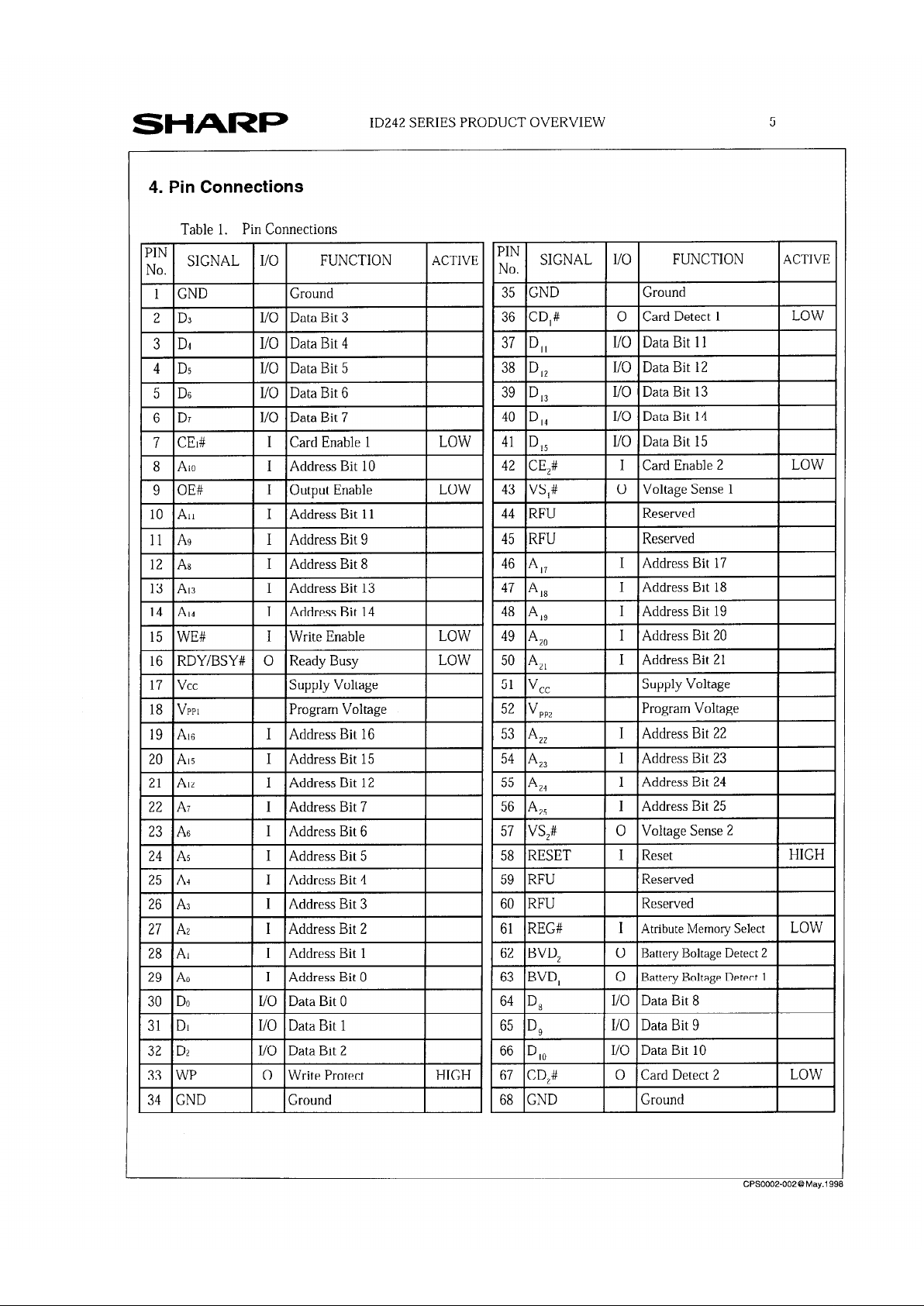
4. Pin Connections
Table 1. Pin Connections
;,” SIGNAL I/O FUNCTION
ACTIVE
LOW
HIGH
1 35 IGND
1 IGround
1 39 ID,,
I I/O I Data Bit 13
I
43 IVS,#
I I
0 Voltage Sense 1
I 44 IRFU 1 1 Reserved
1 1 Reserved
I I 1 Address Bit 17
I 45 IRFU
1 46 IA,,
54 43
55 A74
I Address Bit 23
I Address Bit 24
1 56 IA,,
I I 1 Address Bit 25
1 I I Reset
0 Voltage Sense 2
I 58 IRESET
57 VS,#
I
62 IBVD,
I
0 Battery Boltage Detect 2
63 BVD, 0
Battery Boltage Detect 1
Data Bit 8 64
DR
I/O
65
DQ
I/O Data Bit 9
66 I/O
Data Bit 10
D,Ll
67 CD,#
I -
68 IGND
0 Card Detect 2
1 Ground
CPSOOO2-002 @ May.1 998
SHARP
ID242 SERIES PRODUCT OVERVIEW
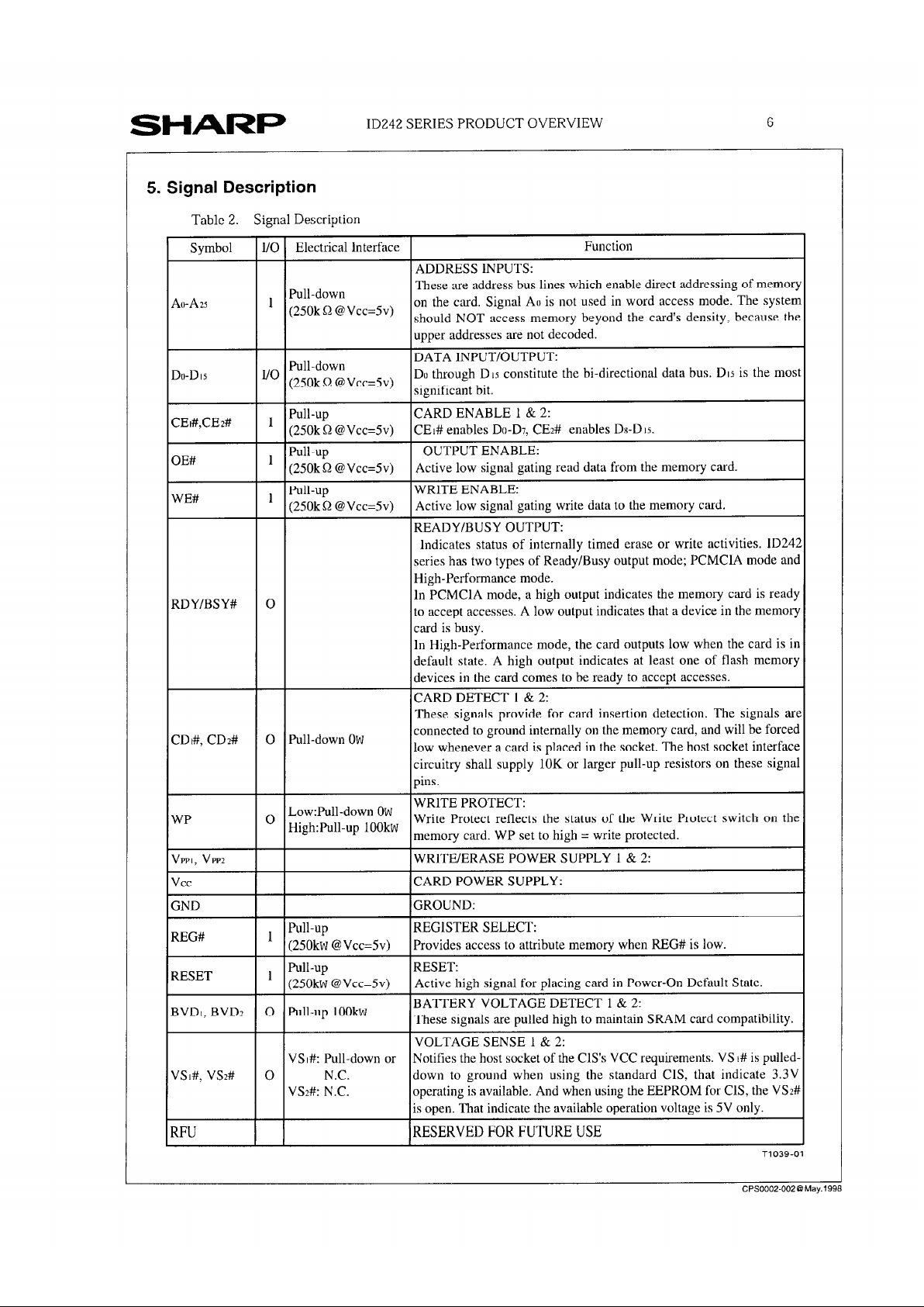
5. Signal Description
Table 2. Signal Description
Symbol l/O Electrical interface
Function
ADDRESS INPUTS:
Ao-Azs
Du-D15
1 Pull-down
These are address bus lines which enable direct addressing of memory
(250k Q @ Vcc=Sv)
on the card. Signal AI) is not used in word access mode. The system
should NOT access memory beyond the card’s density. because the
upper addresses are not decoded.
DATA INPUT/OUTPUT:
1/o Pull-down
(2’0k ’ @VCC=‘V)
De through Dls constitute the bi-directional data bus. DIG is the most
significant bit,
CEI#,CEZ#
OE#
WE#
1 Pull-up CARD ENABLE I & 2:
(250k Q @Vcc=Sv)
CEI# enables Do-D7, CE2# enables Dx-DIG.
1 Pull-up OUTPUT ENABLE:
(250k Q @ Vcc=Sv)
Active low signal gating read data from the memory card.
1 Pull-up WRlTE ENABLE:
(250k 52 @ Vcc=Sv) Active low signal gating write data to the memory c‘ard.
READY/BUSY OUTPUT:
indicates status of internally timed erase or write activities. lD242
series has two types of Ready/Busy output mode; PCMClA mode and
High-Performance mode.
RDY/BSY# 0
In PCMClA mode, a high output indicates the memory card is ready
to accept accesses. A low output indicates that a device in the memory
c,ard is busy.
In High-Performance mode, the card outputs low when the card is in
default state. A high output indicates at least one of flash memory
devices in the card comes to be ready to accept accesses.
CARD DETECT 1 & 2:
These signals provide for card insertion detection. The signals are
CDt#, CD2# 0 Pull-down Ow
connected to ground internally on the memory card, and will be forced
low whenever a card is placed in the socket. The host socket interface
circuitry shall supply 10K or larger pull-up resistors on these signal
pins.
o LowPull-down OW
WRlTE PROTECT:
WP
High:Pull-up 1OOkw
Write Protect reflects the status of the Write Protect switch on the
memory card. WP set to high = write protected.
VPPI,
VW2
WRITE/ERASE POWER SUPPLY 1 & 2:
vcc CARD POWER SUPPLY:
GND GROUND:
REG#
1 Pull-up
REGlSTER SELECT:
(250kw @Vcc=Sv) Provides access to attribute memory when REG# is low.
RESET
1 Pull-up RESET:
(250kw @Vcc=Sv)
Active high signal for placing card in Power-On Default State.
BVDt, BVD2 0 Pull-up 1OOkw
BATTERY VOLTAGE DETECT 1 & 2:
These signals are pulled high to maintain SRAM card compatibility.
VOLTAGE SENSE 1 & 2:
VSI#: Pull-down or Notifies the host socket of the ClS’s
VCC
requirements. VS I# is pulled-
VSI#,
VS2#
0 N.C. down to ground when using the standard ClS, that indicate 3.3V
VSB: N.C. operating is available. And when using the EEPROM for ClS, the VS2#
is open. That indicate the available operation voltage is 5V only.
RFU
RESERVED FOR FUTURE USE
CPSOOOZ-002@Mav.1991
SHARP
ID242 SERIES PRODUCT OVERVIEW 7
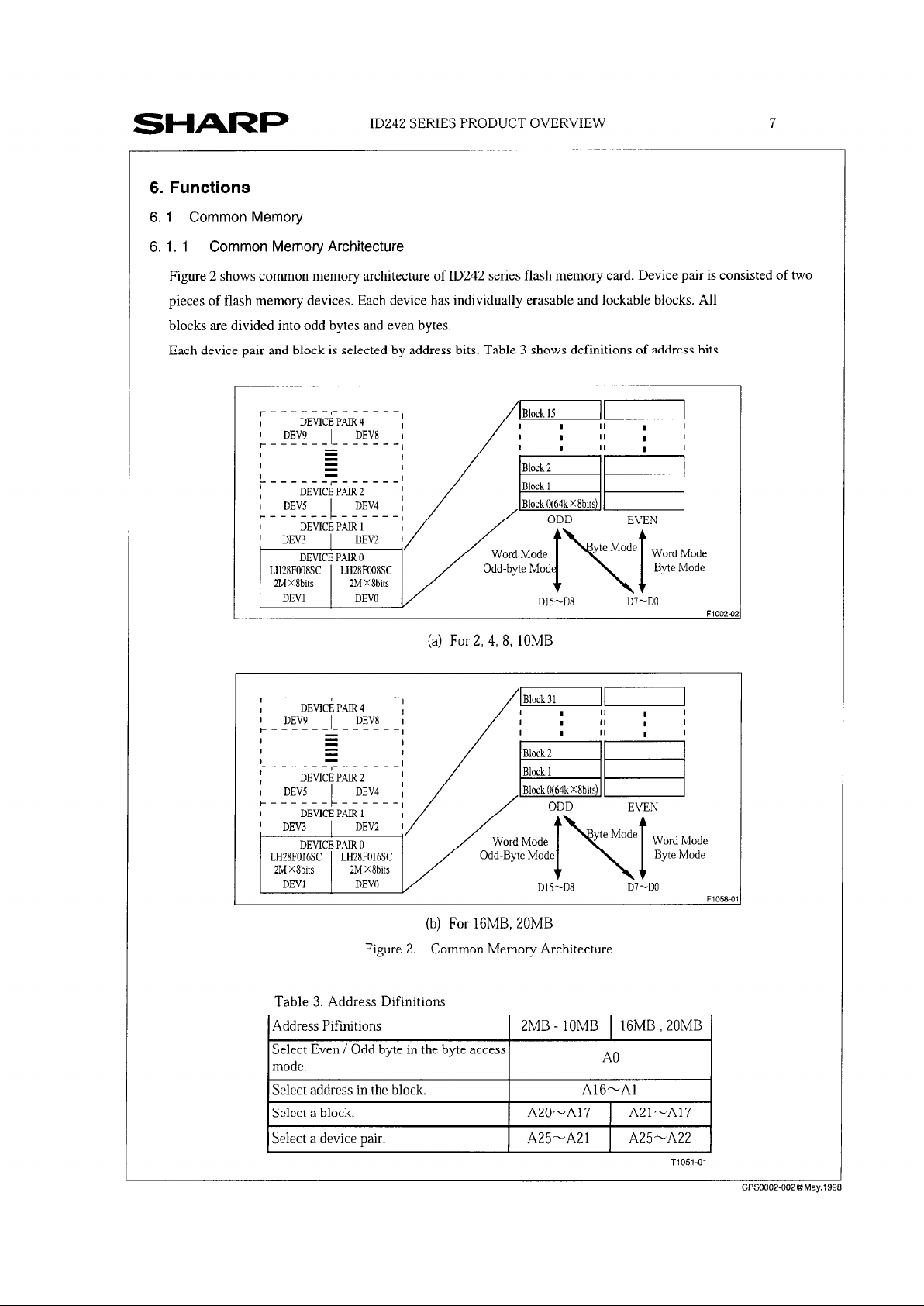
6. Functions
6.1 Common Memory
6. 1. 1 Common Memory Architecture
Figure 2 shows common memory architecture of ID242 series flash memory card. Device pair is consisted of two
pieces of flash memory devices. Each device has individually erasable and lockable blocks. All
blocks are divided into odd bytes and even bytes.
Each device pair and block is selected by address bits. Table 3 shows definitions of address bits.
CPS0002-002OMay.1991 3
F100'2.0:
(a) For 2, 4, 8, 1OMB
F10580'
(b) For 16MB, 20MB
Figure 2. Common Memory Architecture
Table 3. Address Difinitions
Address Pifinitions 2MB - IOMB 16MB ,20MB
Select Even / Odd byte in the byte access
mode.
A0
1 Select address in the block.
I
A16-Al
I
Select a block.
1 A20-A17 1 A21-A17 1
1 Select a device pair. 1 A25-A21 1 A25-A22 1
T1051-01
-
SHARP
ID242SERIESPRODUCTOVERVIEW
8
6. 1. 2 Erase
Erase is executed one block at a time. Erasable block size is 64K bytes in byte access mode and 128K bytes in
word access mode.
6. 1. 3 Address Decoding
The higher address area of ID242 series flash memory card which goes beyond common memory area is not
decoded in common memory access. It means that the system will access to random memory address of the
memory card even if system will try to access to the memory address which exceeds memory capacity of the card.
Please do not access to the memory address which goes beyond memory capacity of the card.
As an enhanced function, the memory card enables to output invalid data (either of OOOOh or FFFFh) when system
will access to the memory address which exceeds memory capacity of the card. Please contact our sales & marketing support to find concrete way of setting.
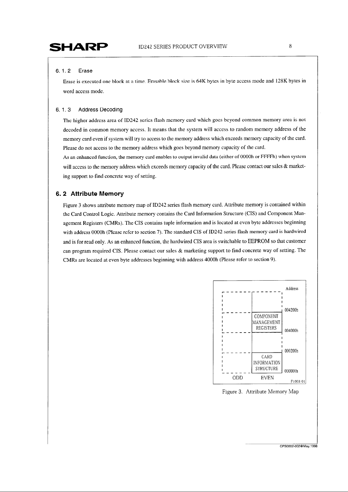
6.2 Attribute Memory
Figure 3 shows attribute memory map of ID242 series flash memory card. Attribute memory is contained within
the Card Control Logic. Attribute memory contains the Card Information Structure (CIS) and Component Management Registers (CMRs). The CIS contains tuple information and is located at even byte addresses beginning
with address OOOOh (Please refer to section 7). The standard CIS of ID242 series flash memory card is hardwired
and is for read only. As an enhanced function, the hardwired CIS area is switchable to EEPROM so that customer
can program required CIS. Please contact our sales & marketing support to find concrete way of setting. The
CMRs are located at even byte addresses beginning with address 4000h (Please refer to section 9).
Address
r-------------,
I
I
I
I
I
I
' 004200h
r-----I
COMPONENT
I
MANAGEMENT
I
I
REGISTERS
c------
_ 004000h
I
I
I
I
I
r------
I 000200h
I
CARD
I
I
INFORMATION
I
STRUCTURE OOOOOOh
------ODD EVEN
F1003-01
Figure 3. Attribute Memory Map
CPSOOOZ-002@ May. 1998

SHARI=
ID242SERIESPRODUCTOVERVIEW
6.3 Function Table
6.3.1 Common Memory Access
Table 4. Common Memory Access
6.3.2 Attribute Memory Access
Table 5. Attribute Memory Access
XXX:Output data is invalid.
The standard CIS is for read only. Write operation is only for CMRs and CIS on EEPROM
7. Card Information Structure (CIS)
The CIS is contained within attribute memory (Please refer to section 6.2). Table 6 shows standard CIS tuples, but
it is for read only. As an enhanced function, the hardwired CIS area is switchable to EEPROM so that customer
can program required CIS. Please contact our sales & marketing support to find concrete way of setting.

SHARP
ID242 SERIESPRODUCTOVERVIEW
10
Table
6.
Standard CIS
Address Value Description
46h
53h S :Product Info
48h 48h H
52h
54h
56h
58h
ah
5Ch
5Eh
60h
62h
64h
49h I
44h D
32h 2
34h 4
53h S
52h R
20h SPACE
OOh END TEXT
53h S :Maker Info
48h H
66h 1 41h IA
68h 52h R
6Ah 1 50h IP
6Ch 20h SPACE
6Eh
43h C
70h 4Fh 0
CPS0002.002@May.i9I
84h I ooh IEND TEXT
86h
88h
FFh End of Tuple
1Ah Configuration Info
Last Index of Configuration Table
92h I 40h ICMRS Base Adress(MSB)
I
Configuration Table Entry 1
-

SHARP
ID242 SERIES PRODUCT OVERVIEW
Table 8. Standard CIS (Continued)
Address 1 Value 1
Description
1 Address 1 Value 1
Description
I I
A4h
1 OCh ]Icc Static 1.2mA
t
1Oh Tuple Link
04h IIndex
104h
iO6h
A6h
A8h
06h ICC Average lOOmA
06h ICC Peak lOOmA 02h Vcc & Vpp
79h IParameter Selection
108h
IOAh
IOCh
I OEh
,
AAh 1 23h ~ICC Powerdown 5OmA
t
I I
ACh 1 79h [Parameter Selection
t
I
I
AEh I D5h IVpp Voltage 5V
t
1lOh
BOh
B2h
7Dh NC OK
1Bh Ipp Static 15OmA
7Dh IICC Average 90mA
7Dh ~ICC Peak 90mA
112h
Il4h
B4h
B6h
75h Ipp Average 80mA
75h Ipp Peak 80mA
116h
1Bh ICC Powerdown 15OmA
79h Parameter Selection
I I
B8h I 52h 11ppPowerdown 50mA
t
118h
1lAh I 8Eh lvpp Voltage 12V
BAh
BCh
1Bh Configuration Table Entry 2
OFh Tuple Link 1lCh 7Dh NC OK
1Bh Ipp Static 15OmA
I I
BEh I 02h IIndex 1lEh
120h
122h
124h
126h
128h
12Ah
12Ch
12Eh
130h
35h Ipp Average 30mA
35h Ipp Peak 30mA
52h Ipp Powerdown 50mA
OOh Null
OOh Null
1Eh Device Geometry
06h Tuple Link
02h Bus: 2bytes
1 lh Erase Block: 64Kbvtes
I
I
CAh I 06h IICC Peak lOOmA
CCh
CEh
23h ICC Powerdown 50mA
79h Parameter Selection
DOh
D2h
D4h
8Eh Vpp Voltage 12V
7Dh NCOK
1Bh Ipp Static 1XhnA
132h 1
Olh Read size: lbyte
134h I Olh IWrite size: lbyte
I D6h I 35h 11pp Average 30mA
I
136h
138h
13Ah
13Ch
13Eh
14Oh
Olh Partation: lblock
Olh Non-interleaved
20h Manufacturer ID
04h Tuple Link
L
BOh
Manufacturer Code
OOh
D8h
DAh
DCh
DEh
EOh
E2h
35h Ipp Peak 30mA
52h Ipp Powerdown 50mA
1Bh Configuration Table Entry 3
1 lh Tuple Link
03h Index
02h Vcc & Vpp
Manufacturer Info:
06h 2MB
07h 4MB
09h 8MB
OAh 1OMB
ODh
16MB
OEh 20MB
33h Manufacturer Info: DVO
E4h
E6h
E8h
79h Parameter Selection
B5h
1Eh
vcc Voltage 3.3v
142h
144h
146h 21h Function Identification
02h Tuple Link
Olh IFunction: MEMORY
OOh ISystem Init: None
148h
14Ah
I
F4h
F6h
FAh
B5h
9Eh
Vpp Voltage 3.3V
1Bh Ipp Static 15OmA
I
14Ch
14Eh FFh End of CIS
I
FCh 75h Ipp Average 80mA
I
FEh 75h Ipp Peak 80mA
IOOh 52h Ipp Powerdown 5OrnA
102h 1Bh Configuration Table Entry 4
I.
CPSOOOZ-002 0 May. 199

SHARP
ID242 SERIES PRODUCT OVERVIEW
12
8. Card Control
8. 1 Reset
The card is in initial state directly after power-up. But we recommend to do reset operation after power-up to
make sure to initialize the card.
During block erase, byte write, or lock-bit configuration modes, an active RESET will abort the operation. RDYI
BSY# remains low until the reset operation completes. Memory contents being altered are no longer valid; the
data may be partially erased or written. The host must wait after RESET goes to logic-Low (Vu) before it can
write another command, as determined by
tPHWL.
It is important to assert RESET to the card during a system reset. If a CPU reset occurs without a card reset, the
host will not be able to read from the card if that card is in a different mode when the system reset occurs.
For example, if an end-user initiates a host reset when the card is in read status register mode, the host will attempt
to read code from the card, but will actually read status register data. Sharp’s ID242 Series Flash Memory Card
allows proper card reset following a system reset through the use of the RESET input.
8. 2 Status Register
Each flash memory device in the card has status register. The status register may be read to determine when a
write, block erase, or lock-bits configuration is complete, and whether that operation completed successfully
(please refer to Table 10). It may be read at any time by writing the Read Status Register command (70h, 7070h)
into the CUI. In word access mode, the status register data of even byte devices are output to D7-0,and the status
register data of odd byte devices are output to D15-8.
8. 3 Write Protect Switch
The ID242 Series Flash Memory Card has a write protect switch on the back of the card. When the switch is in the
write protect position, the card blocks all writes to the common and attribute memory without Card Management
Registers region (see Figure 5).
8. 4 Read identifier Codes / Lock bits Information
Manufacture Code and Device Code are contained within each flash memory device in the memory card. The
identifier code operation is initiated by writing the Read Identifier Codes command (90h, 9090h) into the CUI of
each memory device. The specific address of each device is necessary to be selected to read these codes (Table 8).
I
F1005-01
m
Writeble position
I
I
I
Write protZ&ition
Note: The write protect switch is shown by the black square.
Figure 4. Write Protect Switch
CPS0002.002@May.1998

SHARP
ID242 SERIES PRODUCT OVERVIEW
13
Table 7. Status Register
bit7 bit6 bit5
bit4 bit3 bit2 bit1 bit0
SR.7
WSMS
SR.6
ESS
SR.5
ECLBS
SR.4
BWSLBS
SR.3
VPPS
SR.2
BWSS
SR.l
DPS
SR.0
RFU
SR.7 =WRITE STATE MACHINE STATUS Notes:
I = Ready
0 = Busy Chech RDY/BSY# or SR.7 to determine block erase,
SR.6 =ERASE-SUSPEND STATUS
word/byte write, or lock-bit configuration completion.
SR.6-0 are invalid while SR.7=“0”.
I = Erase Suspended
0 = Erase in Progress/Completed
If both SR.5 and SR.4 are ” 1 “s after a block erase or lock-
SR.5 =ERASE AND CLEAR LOCK-BlTS STATUS
bit configuration attempt, an improper command
1 = Error ln Block Erasure or Clear Lock-Bits
sequence was entred.
0 = Successful Block Erase or Clear Lock-Bits
SR.3 does not provide a continuous indication of V,,
SR.4 =BYTE WRITE AND SET LOCK-BIT STATUS level. The WSM interrogates and indicates the V,, level
1 = Error in Byte Write or
only after Block Erase, Word/Byte Write, Set
Set Block/Master Lock-Bit Block/Master Lock-bit, or Clear Lock-bits command
0 = Successful Byte Write or
sequences. SR.3 is not guaranteed to reports accurate
Set Block/Master Lock-Bit
feedback only when V,,=V,,,,,,,,.
SR.3 =VPP STATUS
1 = VPP Low Detect, Operation Abort
SR. 1 does not provide a continuous indication of master
0 = VPP OK
and block lock-bit values. The WSM interrogates the
master lock-bit, block lock-bit. and RP# only after Block
SR.2 =BYTE WRITE SUSPEND STATUS
Erase, Word/Byte Write, or Lock-bit configuration
1 = Byte Write Suspended
command sequences. If informs the system, depending
0 = Byte Write in Progress/Completed
on the attempted operation, if the block lock-bit is set,
master lock-bit is set, and/or RP# is not 12V. Reading
SR. 1 =DEVICE PROTECT STATUS
the block lock and master lock configuration codes after
1 = Master Lock-bit,Block Lock-bit and/or
writing the Read Identifier Codes commnad indicates
RP# Lock Detected, Operation Abort
master and block lock-bit status.
0 = Unlock
SR.0 =Reserved for Future Enhancements
SR.0 is reserved for future use and should be masked out
when polling the status register.
Table 8. Identifier Codes / Lock bits
Block Lock
Configuration (X: Select Block)
D7-D I: Reserved
NOTE: A0 is ignored in word access mode. and D15-D8 outputs the Odd byte data.
DPA: Address as select device pair
BLKD: Block Lock Configuration Data
MLKD: Master Lock Configuration Data
T1052-01
CPSOOO2-0028 May. 1999

SHARI=
ID242 SERIES PRODUCT OVERVIEW
9. Component Management Registers (CMR)
Component Management Registers (CMR) are mapped at even byte locations beginning at address 4000h in
attribute memory.
9. 1
9. 2
9. 3
9. 4
Configuration Option Register (Address4000h)
Address Bit.7 Bit.6 Bit.5
Bit.4 Bit.3 Bit.2 Bit. 1 Bit.0
4000h SRESET
Reserved
SRESET: l=Reset State O=End Reset Cycle
Card Configuration Register (Address:4002h)
Address
4002h
Bit.7 Bit.6 Bit.5 Bit.4
Bit.3 Bit.2 Bit. 1 Bit.0
Reserved PWDN
Reserved
PWDN: l=Power-Down
Device pairs that apointed by Sleep Control Register(4118h-411Ah) are in PowerDown.
O=Power-Up
Socket and Copy Register (Address:4006h)
Address Bit.7 Bit.6 Bit.5 Bit.4 Bit.3 Bit.2 Bit.1 Bit.0
4006h
Reserved Copy No. Soket No.
Soket No.: Socket Number
Copy No.: Copy Number
The card may use to distinguish between similar cards installed in a system.
TlO53.01
Card Status Register (Address:41 OOh)
Address
41OOh
Bit.7 Bit.6 Bit.5
Bit.4 Bit.3 Bit.2 Bit. 1 Bit.0
ADM ADS SRESET
CMWP PWDN CISWP WP RDY/BSY
ADM: ORed value of the Ready/Busy Mask Register.
1 = Any device is masked. 0 = All Devices are not Masked.
ADS: ORed value of the Sleep Control Register.
I = Any device-pair is Controled power-down by bit.2 of the Card Configuration
Register.
SRESET: Reflects the bit.7 of the Configuration Option Register.
CMWP: Reflects the bit.1 of the Write Protection Register.
PWDN: Reflects the bit.2 of the Card Configuration Register.
CISWP: Reflects the bit.0 of the Write Protection Register.
WP: Indicates the Write Protect Switch status.
I = Write Protect Switch: ON I = Write Protect Switch: OFF
RDY/BSY: Reflects the Ready/Busy Status Register.
1 = All devices are READY. 0 = Any device is BUSY.
CPSOOO2.002 @ May. 1991

SHARI=
ID242 SERIES PRODUCT OVERVIEW 15
9. 5 Write Protection Register (Address:41 04h)
Address Bit.7 Bit.6 Bit.5 Bit.4 Bit.3
Bit.2 Bit.1 Bit.0
4104h Reserved BLKBN CMWP CISWP
BLKBN: Block Locking Enable
1 = Enable Block Locking 0 = All Blocks Unlocked
CMWP: Common Memory Write Protect
1 = Common Memory without CIS region in Write Protect Status
CISWP: Common Memory CIS Write Protect
I = Common Memory CIS in Write Protect Status
NOTE: ID242 series ignores BLKBN bit. Block Locking is always enable.
9. 6 Sleep Control Register (Address:41 18h-411 Ah)
Address
4llAh
4118h
Bit.7 Bit.6 Bit.5 Bit.4 Bit.3 Bit.2 Bit. 1 Bit.0
Reserved
Reserved DEVlO/ll DEV8/9 DEV6/7 DEV4/5 DEV2/3 DEVO/l
1= Select sleep mode device-pair
If set to “l”, the corresponding device-pairs are putted into deep power-down mode
by PWDN bit of Configuration Status Register.
Tl047.01
9. 7 Ready/Busy Mask Register (Address:41 20h-4122h)
Address
412231
4120h
Bit.7
DEV7
Bit.6 Bit.5 Bit.4 Bit.3 Bit.2 Bit. 1 Bit.0
Reserved DEVll DEVlO DEV9 DEV8
DEV6 DEV5 DEV4 DEV3 DEV2
DEVl
DEVO
1 =Mask the RdylBsy#
The corresponding device’s Rdy/Bsy# signals to set bit are ignored for card’s
RDY/BSY# output.
T1040.01
9. 8 Ready/Busy Status Register (Address:41 30h-4132h)
Address
4132h
4130h
Bit.7
DEV7
Bit.6 Bit.5 Bit.4 Bit.3 Bit.2 Bit. 1 Bit.0
Reserved DEVll DEVlO DEV9 DEV8
DEV6 DEV5
DEV4
DEV3
DEV2 DEVl
DEVO
1 =READY
O=BUSY
Each bit indicates the corresponding device’s Rdy/Bsy# signal.
Tl041.01
9. 9 Ready/Busy Mode Register (Address:4140h)
Address
4140h
Bit.7 Bit.6 Bit.5 Bit.4
Reserved
RACK: Ready Acknowledge Bit
Bit.3 Bit.2 Bit. 1 Bit.0
RACK MODE
Must-clear this bit after receiving ready status to prepare for next device’s ready
transition.
MODE: RDY/BSY# Mode
1 = High-Performance Mode 0 = PCMCIA Mode
T1055.01
CPS0002-002@May.l99i

SHARP
ID242SERIESPRODUCTOVERVIEW
IO. Command Definitions
Device operations are determined by writing specific commands to the Command User Interface. Table 9 defines
the commands.
Table 9. Command Definitions
-r
1
Command
Second Bus Cycle
gate
First Bus Cycle
Address 1 Data
Operation
Write
1
Write
E
2 Write
Write
3peration
Address
Data
DA
FFh
(PFl+)
DA
DA
DA
WA
BA
DA
90h
(9090h)
70h
(707Oh)
50h
(5050h)
40h
(4040h)
or
1Oh
(1010h)
20h
(2020h)
BOh
(BOBOh)
DA
DOh
(DODOh)
BA
DA
DA
60h
(6060h)
60h
(6060h)
60h
(6060h)
(
Read Array / Reset
Read Identifier Codes
Read
Read
Read Status Register
Zlear Status Register
WA 1 WD
WordlByte Write
Read
3
Write
I
Write
Block Erase
3
Write
3 Write
3 Write
Write
4 Write
Write
Data
Block Erase and Word/Byte Write
Suspend
Block Erase and Word/Byte Write
Resume
Set Block Lock-Bit
Write
Set Master Lock-Bit
Write
Write
Clear Block Lock-Bit
Address
IA =Identifier code Address
WA
=Write Address
ID
WD
=Identifier Codes
=Write Data
BA
DA
=Block Address
=Device Address
SRD
=Data from Status Register
Note:
1. Following the Read Identifier Codes command, read operations access manufacture, device, block lock, and
master lock codes.
2. Status Register may be read to determine when a write, block erase, or lock bit configuration is complete,
and whether that operation completed successfully.
3. If the block is locked, block erase or write operations are desabled.
4. This command is not available.
CPSOOOZ-002@ May.1991

SHARP
ID242 SERIES PRODUCT OVERVIEW
11. Electrical Specifications
11. 1 Absolute Maximum Ratings
NOTES:
1. Operating temperature is for commercial product defined by this specification.
2. All specified voltages are with respect to GND. During transitions, this level may undershoot to -2.0~ for
periods 4!0ns or overshoot to Vcc+2.Ov for periods <20ns.
Il. 2 Recommended Operating Conditions
11.3 Capacitance
PARAMETER
Input Capacitance
Input/Output Capacitance
SYMBOL MIN
cm C,” -
TYP MAX
15 25 -
UNIT
PF
PF
Ta=25”C, f=lMHz
CONDITION
v,,=o.ov
vO,,=O.Ov
11. 4 AC Input/Output Test Conditions
Vcc=3.3V-+Q.3V
;oy)Lp$iq+~
Vcc=5Vk5%
3s
Or
vcc=5vs-lo%
1,5 T$q$=XT F,008-0,
Figure 5. Transient Input/Output Reference Waveform
Figure 8 shows Input/Output level and test level for AC test. Input rise and fall times (10% to 90%) < 10ns.
ws""uz-owdMay.199<

SHARP
ID242 SERIES PRODUCT OVERVIEW 18
12. DC Characteristics
(Ta = 0 to 60°C)
NO-
TE
-i-
iYM
BOL
RI2
JOLI
VTOHI
dOH2
CCS
CCD
CCR
ccw
I
I
I
4
4
4
\
1
‘CE
679
TWS
?xs
‘LKO
TEST CONDITION
T1042-01
PARAMETER
nput Low Voltage
nput High Voltage
nput Low Current
nput High Current
jutput Low Voltage
jutput High Voltage
‘cc Stand-by Current
\,
‘cc Deep Power-Down
C hrrent
\
‘cc Read Current
v
‘cc Word Write or Set
L .ock-Bit Current
V cc Block Erase or
C lear Lock-Bit Current
Lock Erase Suspend
:ontinue to next page
I
2
3
3
2
4,5
4
5
68
69
6
CPSOOOZ-0028 May. 199.9

SHARI=
ID242SERIESPRODUCTOVERVIEW
DC Characteristics (Continued)
(Ta = 0 to 60°C:
T/+KAIVIC ICK , BOL , TE ,
ry
MIN MAX , ;I;., v k;; 1 UNIT 1
TEST CONDITION
I I
vrrs vcc
\ T,,Stmd-by or Read
C :urrent
\
Ipp Deep Power-Down
C :urrent
6
4MB 1
I 0.8 I
8MB 1.6
1.6 mA
VPF>VCC
1OMB 2.0 2.0 mA
16MB 1.6 1.6 mA
20MB 1 I 2.0 I I 2.0
UA
---I
UA
6
’ \
Word Write or Set
L Zk-Bit Current
6.9 vrr=5.0v* 10%
\ I,,,, Block Erase or
C blear Lock-Bit Current
v I,+, Word Write or
B lock Erase Suspend
C ‘urren t
V
6.9
40
40
mA IVrr=5.0Vt 10%
32 32 mA I Vrr=l2.OVf 5%
2MB 400 400
UA
4MB 430 430
---I UA
8MB 500 500
UA
4
VW5 vcc
1OMB 530 530
bA
16MB 500 500
UA
20MB 1
I
530
I
I
530
uA I
6
2MB I
I
0.4
I I
0.4
4MB 1
I 0.8 I
1 0.8
8MB 1
I 1.6 I I
1.6
VPP>VCC
1OMB 2.0 2.0
16MB 1.6
1.6
20MB 2.0 2.0
Ipp Lockout Voltage VrTLK 7,9
I 1 1.5 1 1 1.5 1 v 1
71048-01
NOTE:
1. These parameters are applied to all input pins and all i/put/output pins in input mode.
2. These parameters are applied to An-AZ5 and Do-D,, in input mode.
3. These parameters are applied to CE,#.CEz#,WE#,OE#,REG# and RESET.
4. These parameters are applied to RDY/BSY#.
5. These parameters are applied to Do-D,, in output mode.
6. All currents are in RMS unless otherwise notes.
7. Block erase, word/byte write, and lock-bit configurations are inhibited when V,,, 5 VFPLK, and guaranteed in
the VPP Voltage is VPI’I, VFPZ or VFI.I.
8. Automatic Power Savings(APS) reduces typical I
CCK to 30mA at Vcc=SV and 20mA at Vcc=3.3V in static
operation.
9. Sampled.
CPSOOO2.002@ May. 1998

ID242 SERIES PRODUCT OVERVIEW 20
13. AC Characteristics
Testing Conditions :
1) Input Pulse Level
2) Input Rise/Fall Time
3) Input/Output Timing Reference Level
4) Output Load
(including scope and jig capacitance)
13. 1 Common Memory Read Operations
PARAMETER
Read Cycle Time
Address Access Time
CE# Access Time
OE# Access Time
Output Disable Time from
CEl#,CE2# *
Output Disable Time from
OE# *
Output Enable Time from
CEI#,CE2#
Output Enable Time from
OE#
Data Valid Time from
Address Change
+:Time until output become
1.5 to 3.w (@vcc=5v~5%,vcc=5v+10%)
0 to 3.ov (@Vcc=3.3+0.3V)
Ions
2.5V (@Vcc=5V~5%,Vcc=SV~lO%)
1.5v (@Vcc=3.3V+O.3V)
lTTL+lOOpF (@VCC=~V+~%,VCC=~V+IO%)
lTTL+SOpF (@Vcc=3.3V+O.3V)
(Ta = 0 tc
SYMBOL vcc=3.3vi ON Vcc=SV~ 5%
vcc=w-t 10%
IEEE
JEIDA/
PCMCIA
MIN MAX MIN MAX MIN MAX
t
AVAV
tcR
250 - 150 - 160 -
t
AVQV
t,(A) - 250 - 150 - 160
t
ELQV
t,(CE) - 250 -
150 -
160
. . .
1 t,(OE) 1 - 1 125 1 - 1 75 1 - 1 80
kHQz ItdidCE) 1 - 1 100 1 - 1 75 I - 1 80
t
- -
- 80
GHQZ
QOE)
100 75
tE
LQNZ
tc,,( CE) 5 - 5 - 5 -
WV
0 - 0 - 0 -
, floating. (The output voltage is not defined.)
60°C)
~ Unit
ns
rio43ai
CPS0002.002@May.1991 9

SHARP
ID242 SERIES PRODUCT OVERVIEW
Address
CEl#, CE2#
OE#
Dout
Figure 6. AC Waveforms for Read Operations
Note) 1. WE# = “HIGH”, during a read cycle.
2. Either “HIGH” or “LOW” in diagonal areas.
3. The output data becomes valid when last interval, ta (A), ta (CE) or ta (OE) have concluded.
CPS0002-002QMay.199

SHARP
ID242 SERIES PRODUCT OVERVIEW
22
13.2 Command Write Operations : Common Memory
13. 2. 1 WE# Controlled Write Operations
PARAMETER
Write Cycle Time
Address Setup Time
Write Recovery Time
Data Setup Time for WE#
Data Hold Time
OE# Hold Time from
WE#
CE# Setup Time for WE#
Address Setup Time for
WE#
Write Pulse Width
WE# High to RDY/BSY#
going Low
RESET Recovery Time
VPP Setup Time
VPP
Hold Time
Word/Byte Write Time
Block Erase Time
jet Lock-Bit Time
Zlear Block Lock-Bits
rime
Nor-d I byte Suspend Latency
rime to Read
Gase Suspend Latency Time
o Read
(vcc=3.3Vi
0.3VTa=O to 60°C)
t\ “HRH I
t
WHRHZ
vw=3.3v k 0.3%
vPP=w+
10%
vw= 12v -t 5%
vpp=3.3vi- 0.3%
VPP=5Vt
10%
vrr=12v* 5%
10.0
PS
9.3
P s
10.4
PS
21.1
PS
17.2
l-1 s
17.2
I-is
T1044.01
CPSOOOZ-0028 May. 199

SHARI=
ID242 SERIES PRODUCT OVERVIEW
PARAMETER
Write Cycle Time
Address Setup
Time
Write Recovery Time
Data Setup Time for WE#
Data Hold Time
OE# Hold Time from
WE#
CE# Setup Time for WE#
Address Setup Time for
WE#
Write Pulse Width
WE# High to RDY/BSY#
going Low
RESET Recovery Time
VPP
Setup Time
VPP
Hold Time
Word/Byte Write Time
Block Erase Time
Set Lock-Bit Time
Clear Block Lock-Bits
Time
Word I byte Suspend Latency
Time to Read
Erase Suspend Latency Time
to Read
(Vcc=5Vi 5%, Vcc=5Vi lOsTa = 0 I
60°C)
Unit
ns
ns
ns
ns
ns
ns
ns
ns
ns
ns
PS
ns
ns
PS
PS
S
S
PS
r1049-oi
CPSOOOZ-0026May.199

SHARP
ID242 SERIES PRODUCT OVERVIEW
1. 2. 3. 4. 5.
6.
VIH
Address
Vn.
VIH
CE#, CE2#
VIL
hH
OE#
VTL
‘VALID
DATA
~ sm
tPHWL
hvmL
VOH
RDYIB SY#
VOL
I
,
I
VIH
RESET
VIL
IT
tQVVL
--
VPP I .ZJ
VPP
FL
Figure 7. AC Waveforms for Write Operations (WE# Controlled)
Note)
While the data signal is in output mode, do not apply an opposite phase input signal.
CPS0002.0020May.199

SHARP
ID242SERIESPRODUCTOVERVIEW
13. 2. 2 CE# Controlled Write Operations
PARAMETER
Write Cycle Time
Address Setup Time
Write Recovery Time
Data Setup Time for CE#
Data Hold Time
OE# Hold Time from CE#
WE# Setup Time for CE#
Address Setup Time for
CE#
Write Pulse Width
CE# High to RDY/BSY#
going Low
RESET Recovery Time
VPP Setup Time
VPP
Hold Time
Word/Byte Write Time
Block Erase Time
Set Lock-Bit Time
Clear Block Lock-Bits
Time
Word I byte Suspend
Latency
Time to
Read
Erase
Suspend
Latency Time
to Read
(Vcc=3.3Vt- 0.3\(Ta = Oto 60°C)
t
EHRHI
t
EHRH2
VPP4V~ 10%
vPP=lzv* 5%
vpp=3.3v-t 0.3v
Vpr=5VIk 10%
vPP=lzvk 5%
9.3 !JS
10.4
PS
21.1
I-1 s
17.2
PS
17.2
PS
T1045-01
CPS0002.002@May.199
J
a

SHARI=
ID242 SERIES PRODUCT OVERVIEW 26
1
PARAMETER
Write Cycle Time
Address Setup Time
Write Recovery Time
Data Setup Time for CE#
Data Hold Time
OE# Hold Time from CE#
WE# Setup Time for CE#
Address Setup Time for
CE#
Write Pulse Width
CE# High to RDY/BSY#
going Low
RESET Recovery Time
VPP
Setup Time
VPP
Hold Time
Word/Byte Write Time
Block Erase Time
Set Lock-Bit Time
Clear Block Lock-Bits
Time
Word I Byte
Suspend Latency
Time to Read
Erase Suspend Latency Time
to Read
(Vcc=5V& 5%, Vcc=SV& IO%, Ta=O to 60°C
T1046-01

SHARB=
ID242 SERIES PRODUCT OVERVIEW
27
Address
wE#
OE#
CE#, CE2#
DATA
1. 2.
3. 4. 5.
6.
k,(A)
tcw
1 1 tsu(A-CEH) k&E)/
k’HEL
tEHRHl.2
tEHRL
VOH
RDYlBSY#
VOL
I
/
vm
RESET
RL
1
%%22
VPP
FL
1. v,, tAg~zIzGs9https://manualmachine.com//Y
V,, POWER-UP AND STANDBY
2. /cl~~~~4tVM~~.17~~~~aj;/~~~~~~M~~.~~~F~P~~q
WRITE DATA WRITE OR ERASE SETUP COMMAND
3. 7j;‘Lx++J (,Y~P~~~)‘bfil;f;)‘~~il~~7~~~~~~~
WRITE VALID ADDRESS AND DATA OR ERASE COMFIRM COMMAND
4. $1/Yi-~~~~~filf$~)A~;C~aa~~
AUTOMATED DATA WRITE OR ERASE DELAY
5. x~-~Jz.b-%7b~~~~~xL
READ STATUS REGISTER DATA
6. ~-F-~%~~z+‘~W~&A&
WRITE READ ARRAY COMMAND
Figure 8. AC Waveforms for Write Operations (CE# Controlled)
Note)
While the data signal is in output mode, do not apply an opposite phase input signal.

SHARP
ID242 SERIES PRODUCT OVERVIEW
13.3
Attribute Memory Read Operation
(Ta=O-60°C)
PARAMETER
* : Time until becomes floating. (The output voltage is not defined)
T1056-01
Note) When the CIS constructed by EEPROM, this card requires 5V voltage for Vcc.
Address
:El#, CE2#
\
t,(A)
e w
h(A)
1
c
\
/
\
/
ta(CE)
w
OE#
\\\\\\\\A
i/ ’ / ’ ’ ’ ’ ‘/ ’ / /
/
t&W
L&E) I
tdOE) ~
t&W
e A
t
f-%%hms
Dout
r q&Y-&T
Data Output is valid
High-Inpedance
F1009-0;
I
Figure 9. Attribute
Memory Read Operation
CPSOOOZ-00263May.1996

SHARP
ID242 SERIES PRODUCT OVERVIEW
13.4 Attribute Memory Write Operation
(Ta=O-60°C)
I
SYMBOL
vcc=3.3v* 0.3v
1 vcc=.wi 10% 1
PARAMETER
PCMCIA
I
Unit
MAX MIN MAX
I I I
-
ns
Write Pulse Width
Setup Time for OE#
1 Hold Time for OE#
Setup Time for CE#
_....-
I .-\--
It
1.lllr.T
1 t, (OE-\i
Hold Time for CE#
I.. . ..l
“.‘\- - -- -
t
WLWH
‘w(WE)
300 150
ns
t
35
10
ns
CHWI twIOE-WE)
W
35
10
ns
, “““~I. , II.
t
F1 u/H
ILfCF.~
0
0 ns
35
20 ns
ll....
I .“’ \ - -/
t
CHEH
t,, W
I
I
T1057-01
Note) When the CIS constructed by EEPROM, this card requires 5V voltage for Vcc.
Address
CEl#, CE;?#
OE#
WE#
DATA
VIH
VIH
\
AIN
t,,(OE-WE)
VIH
F1057-01
Figure 10. Attribute Memory Write Operation

SHARP
ID242 SERIES PRODUCT OVERVIEW
13.5 Power-Up/Power Down
PARAMETER
SYMBOL
PCMCIA
NOTES MIN MAX
UNITS
CE# Signal Level (O.OV < Vcc < 2.OV) Vi (CE)
1
0
ViMAX
V
CE# Signal Level (2.OV < Vcc < Vin) 1 vcco. I
ViMAX
V
CE# Signal Level (Vtu < Vcc) 1
VIH
ViMAX
V
CE# Setup Time
tsu WCC)
-
20
-
ms
I I I I
I
RESET Setup Time
tau WSET)
-
20
-
ms
CE# Recover Time
tree WCC)
-
1.0
-
IJS
VCC Rising Time
b
2
0.1 300
ms
VCC Falling Time
tPf
2
3.0 300
ms
1
RESET Width tw (RESET)
I - I
10 I - I us -I
RESET Width
RESET Width
th (Hi-Z RESET)
ts (Hi-Z RESET)
-
-
1
-
ms
0
-
ms
NOTES:
1. ViMAx means Absolute Maximum Voltage for input in the period of O.OV < Vcc < 2.0 V, Vi (CE#) is only
o.oov-ViMAX
2. The tpr and tpr are defined as “linear waveforms” in the period of 10% to 90%, or vice-versa. Even if the
waveform is not a “liner waveform,” its rising and falling time must meet this specification.
e e
tPr tPr
-c- tsu WCC) - -c- tsu WCC) vcc vcc
-)- tsu (RESET) -)- tsu (RESET) = =
-- --
th (Hi-Z RESET) th (Hi-Z RESET)
Hi-Z
-3
RESET n
tw (Hi-Z RESET) +
:Et#, CEa#
At-
ts (Hi-Z RESET)
Hi-Z
FlOlZ-01
Figure 11. Power- Up/Uown liming
CPSOOO2.002 0 May. 1991

SHARI=
ID242 SERIES PRODUCT OVERVIEW
31
14. Specification Changes
This datasheet is for ID242 series product overview, and final specifications will be submitted for qualification of
the memory card. Please note that contents of this datasheet may be revised without announcement beforehand.
Please do NOT finalize a system design with this information.
15. Other Precautions
Permanent damage occurs if the memory card is stressed beyond Absolute Maximum Ratings. Operation
beyond the Recommended Operating Conditions is not recommended and extended exposure beyond the
Recommended Operating Conditions may affect device reliability.
Writing to the memory card can be prevented by switching on the write protect switch on the end of the
memory card.
Avoid allowing the memory card connectors to come in contact with metals and avoid touching the connectors, as the internal circuits can be damaged by static electricity.
Avoid storing in direct sunlight, high temperatures (do not place near heaters or radiators), high humidity and
dusty areas.
Avoid subjecting the memory card to strong physical abuse. Dropping, bending, smashing or throwing the
card can result in loss of function.
When the memory card is not being used, return it to its protective case.
Do not allow the memory card to come in contact with fire.

ID242SERIESPRODUCTOVERVIEW
16. External Diagrams
1
0
A ENLARGEMEHT of THE
WRITE-PROTECT SWITCH
- -
Protected
(Substrdtc
Aped)
FRONT
BACK
A--P
r-
SCALE UNIT
A,PPLICIILL
l/l
mm
CH- DATE REVISE CHARGl
THICKNESS MATER1 AL FlNISk
MEMORY CARD
NAt7E
EXTERNAL DIAGRAM
I
OATE
,997. 9. 8 I
Bltla* OLlY TRIEFCI(ECR A,rn.l
wd matngaa P~vI*rt Team
PCMCIA Ret. 2. 0 TYPE1
\kU~UydtiA
Ic GROUP
SHARP CORPORATION oe*v’rc Morn
IMC026-A103
CPSOOO2-002 BY.199
 Loading...