

Page 1
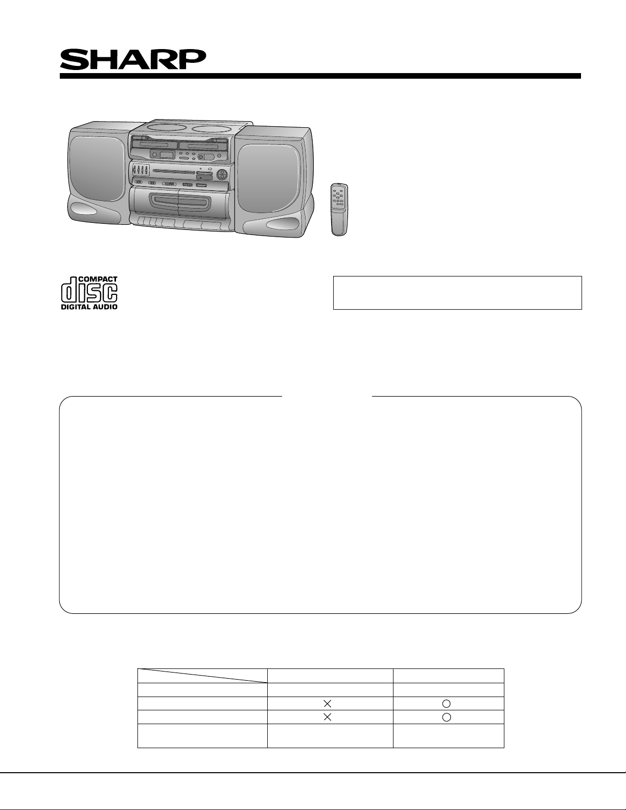
Illustration: GX-CH170Z
GX-CH170X/CH170Z
SERVICE MANUAL
No. S6631GXCH170Z
GX-CH170X
GX-CH170Z
• In the interests of user-safety the set should be restored to its
original condition and only parts identical to those specified
should be used.
CONTENTS
Page
SPECIFICATIONS ............................................................................................................................................................. 2
VOLTAGE SELECTION (GX-CH170Z ONLY)................................................................................................................... 2
NAMES OF PARTS ........................................................................................................................................................... 3
REMOTE CONTROL ......................................................................................................................................................... 4
DISASSEMBLY.................................................................................................................................................................. 5
REMOVING AND REINSTALLING THE MAIN PARTS..................................................................................................... 7
FITTING OF DIAL POINTER ............................................................................................................................................. 8
ADJUSTMENT ................................................................................................................................................................... 9
TROUBLESHOOTING (CHANGER/CD SECTION) ........................................................................................................ 11
NOTES ON SCHEMATIC DIAGRAM .............................................................................................................................. 16
TYPES OF TRANSISTOR AND LED............................................................................................................................... 16
BLOCK DIAGRAM ........................................................................................................................................................... 17
SCHEMATIC DIAGRAM / WIRING SIDE OF P.W.BOARD............................................................................................. 20
WAVEFORMS OF CD CIRCUIT...................................................................................................................................... 35
FUNCTION TABLE OF IC................................................................................................................................................ 36
LCD SEGMENT ............................................................................................................................................................... 37
PARTS GUIDE/EXPLODED VIEW
DIFFERENCE BETWEEN GX-CH170X AND GX-CH170Z
GX-CH170X
TUNER 2 BAND 4 BAND
FINE TUNING
FM STEREO INDICATOR
POWER SOURCE AC 220-240 V,50 Hz AC 110-127/220-240 V,
GX-CH170Z
50/60 Hz
SHARP CORPORATION
Page 2
GX-CH170X/CH170Z
FOR A COMPLETE DESCRIPTION OF THE OPERATION OF THIS UNIT, PLEASE REFER
TO THE OPERATION MANUAL.
SPECIFICATIONS
General
Power source: AC 220-240 V, 50 Hz
(GX-CH170X) DC 12 V [ "D" size (UM/SUM-1,
R20 or HP-2) battery x 8]
Power source: AC 110-127/220-240 V, 50/60 Hz
(GX-CH170Z) DC 12 V [ "D" size (UM/SUM-1,
R20 or HP-2) battery x 8]
Power consumption: 55 W
Output power: PMPO; 60 W (total)
MPO (Max.); 24 W (12 W + 12 W)
(AC operation)
RMS; 10 W (5 W + 5 W)
(DC operation, 10 % T.H.D.)
Output terminal: Headphones; 16 - 50 ohms
(recommended; 32 ohms)
Dimensions: Width; 290 mm (11-1/2")
Height; 260 mm (10-1/4")
Depth; 277 mm (10-15/16")
Weight: 4.3 kg (9.5 Ibs.) without batteries
Compact disc player
Type: Twin CD mechanism
Signal readout: Non-contact, 3-beam semi-
conductor laser pickup
Audio channels: 2
D/A converter: 1-bit D/A converter
Decoder: 16-bit linear quantization
Filter: 4-tims oversampling digital filter
Wow and flutter: Unmeasurable
(less than 0.001% W. peak)
Radio
Frequency range: FM; 87.6 - 108 MHz
(GX-CH170X) AM; 530 - 1,702 kHz
Frequency range: FM; 88 - 108 MHz
(GX-CH170Z) MW; 526.5 - 1,606.5 kHz
SW1; 2.3 - 7.3 MHz
SW2; 7.3 - 22 MHz
Tape recorder
Frequency response: 50 - 14,000 Hz (Normal tape)
Signal/noise ratio: 50 dB (TAPE 1, recording /
playback)
55 dB (TAPE 2, playback)
Wow and flitter: 0.25 % (WRMS)
Motor: DC 12 V electric governor
Bias system: AC bias
Erase system: AC erase
Speaker section
Type: 2-way 4-speaker bass-reflex type
Speakers: 10 cm (4") woofer x 2
Tweeter x 2
Maximum input power: 8 W
Impedance: 3.2 ohms
Dimensions: Width; 190 mm (7-1/2")
Height; 260 mm (10-1/4")
Depth; 183 mm (7-1/4")
Weight: 1.3 kg (2.9 Ibs.) /each
Specifications for this model are subject to change without
prior notice.
VOLTAGE SELECTION (GX-CH170Z ONLY)
Before operating the unit on mains, check the preset voltage.
If the voltage is different from your local voltage. Slide the AC
power supply socket cover by slightly loosing the screw to the
visible indication of the side of your local voltage.
92LCoRD577BQACCB0004AW00
QACCE0007AW00 92LPLUG027 92LPLUG155A
Figure 2 AC POWER SUPPLY CORD AND AC PLUG ADAPTOR
– 2 –
Page 3
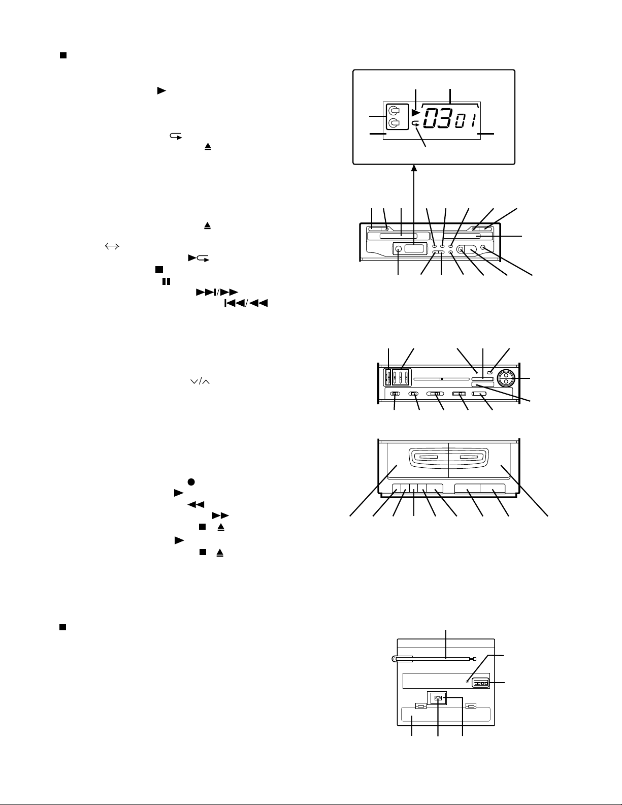
NAMES OF PARTS
Main unit (Illustration: GX-CH170Z)
1. Disc Number Indicator
2. Random Indicator
3. CD Play Indicator:
4. Track Number/Minutes and Seconds/Volume Level/
Programme Number Indicator
5. Programme Indicator
6. CD Repeat Indicator:
7. (DISC 1) Open/Close Button:
8. (DISC 1) Indicator
9. (DISC 1) Disc Tray
10. Random Play Button
11. Clear Button
12. Programme Button
13. (DISC 2) Indicator
14. (DISC 2) Open/Close Button:
15. (DISC 2) Disc Tray
16. DISC 1 2 Select Button
17. (CD) Play/Repeat Button:
18. (CD) Stop Button:
19. (CD) Pause Button:
20. (CD) Track Up/Cue Button:
21. (CD) Track Down/Review Button:
22. Remote Control Sensor
23. Extra Bass Control: X-BASS
24. Graphic Equalizer Controls
25. Stand-By Indicator
26. Tuning Control
27. Power Button
28. Volume Up/Down Button:
29. FM Stereo Indicator (GX-CH170Z ONLY)
30. Dubbing Speed/Beat Cancel Switch
31. Band Selector Switch (GX-CH170X)
31. Tape Selector/FM Mode Switch (GX-CH170Z)
32. Function Selector/Remote Control Switch
33. Band Selector Switch (GX-CH170Z ONLY)
34. Fine Tuning Control (GX-CH170Z ONLY)
35. (TAPE 1) Cassette Compartment
36. (TAPE 1) Record Button:
37. (TAPE 1) Play Button:
38. (TAPE 1) Rewind Button:
39. (TAPE 1) Fast Forward Button:
40. (TAPE 1) Stop/Eject Button:
41. (TAPE 2) Play Button:
42. (TAPE 2) Stop/Eject Button: /
43. (TAPE2) Cassette Compartment
/
1
2
7
23
GX-CH170X/CH170Z
34
1
2
RANDOM
VOLUME
PROGRAM
5
6
1011 12 13
98
14
22 2120 1918 17
24 25 26 27
30
31 32 33 34
383736 3940 41 4235 43
15
16
28
29
Rear panel
44. FM Telescopic Rod Aerial (GX-CH170X)
44. FM/SW Telescopic Rod Aerial (GX-CH170Z)
45. Headphone Socket
46. Speaker Terminals
47. Battery Compartment
48. AC Power Input Socket
49. AC Voltage Selector (GX-CH170Z ONLY)
– 3 –
47
44
48
45
46
49
Page 4
GX-CH170X/CH170Z
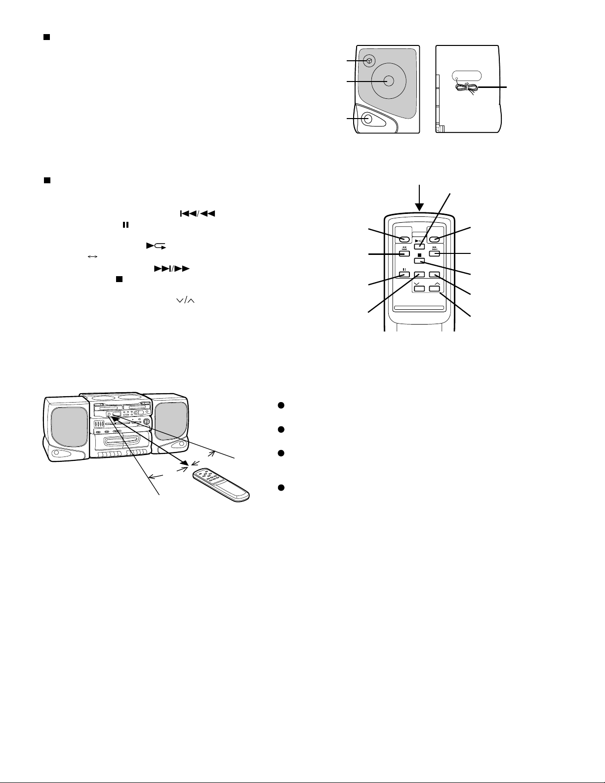
Speaker section
1. Tweeter
2. Woofer
3. Bass Reflex Port
4. Speaker Wire
1
2
3
4
Remote Control
5. Remote Control Transmitter LED
6. Power Button
7. Track Down/Review Button:
8. Pause Button:
9. Random Button
10. Play/Repeat Button:
11. DISC 1 2 Select Button
12. Track Up/Cue Button:
13. Stop Button:
14. Programme Button
15. Volume Up/Down Buttons:
(Illustration: GX-CH170X)
0.3 m - 6 m
(12" - 20')
25˚
REMOTE CONTROL
Notes concerning use:
Replace the batteries if control distance decreases or operation becomes erratic.
Periodically clean the transmitter LED on the remote control
and the sensor on the main unit with a soft cloth.
25˚
Exposing the sensor on the main unit to strong light may interfere with operation. Change the lighting or the direction of
the unit.
Keep the remote control away from moisture, excessive heat,
shock, and vibrations.
6
7
8
9
5
10
11
12
13
14
15
– 4 –
Page 5
DISASSEMBLY
Caution on Disassembly
Follow the below-mentioned notes when disassembling the
unit and reassembling it, to keep it safe and ensure excellent
performance:
1. Take cassette tape and compact disc out of the unit.
2. Be sure to remove the power supply plug from the wall
outlet before starting to disassemble the unit.
3. Take off nylon bands or wire holders where they need be
removed when disassembling the unit. After servicing the
unit, be sure to rearrange the leads where they were
before disassembling.
4. Take suffcient care on static electricity of integrated
circuits and other circuits when servicing.
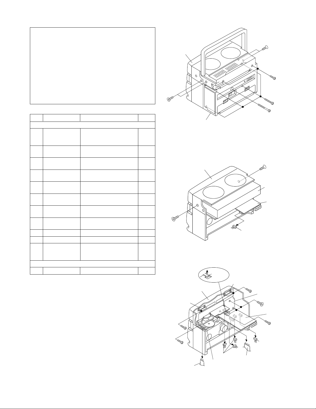
STEP REMOVAL PROCEDURE FIGURE
UNIT
1 Front Cabinet 1. Screw.................. (A1) x11 5-1
2. Socket...................(A2) x1 5-2
3. Tip.........................(A3) x1 6-5
2 CD Block 1. Screw....................(B1) x2 5-2
2. Socket...................(B2) x3 5-3
3 Graphic EQ. PWB 1. Screw ................... (C1) x3 5-3
2. Socket.................. (C2) x1
4 Tuner PWB 1. Screw ................... (D1) x2 5-3
(with Tuner Frame) 2. Flat Cable .............(D2) x1
5 Main PWB 1. Hook .....................(E1) x1 5-3
2. Flat Cable............. (E2) x3 5-3,6-1
6 Display PWB/ 1. Screw .................... (F1) x9 5-3,6-1
Switch PWB 2. Hook ..................... (F2) x1 6-1
7 Deck PWB 1. Screw................... (G1) x3 6-1
2. Socket.................. (G2) x3
8 Tape Mechanism 1. Open the cassette holder.
2. Screw................... (H1) x6 6-2
9 CD Servo PWB 1. Screw.................... (J1) x2 6-3
10 CD Mechanism 1. Screw....................(K1) x6 6-4
11 Power PWB/ 1. Open the battery lid.
Terminal PWB 2. Screw .................... (L1) x4 6-5
3. Hook ..................... (L2) x1
SPEAKER
1 Front Panel 1. Screw .................. (N1) x4 6-6
( A1 ) x2
ø3 x6mm
( B1 ) x1
ø3 x10mm
Front
Cabinet
Switch
PWB
Rear
Cabinet
Front
Cabinet
Front
Cabinet
Figure 5-1
Figure 5-2
( E1 ) x1
GX-CH170X/CH170Z
( A1 ) x2
ø3 x6mm
( A1 ) x2
ø3 x10mm
( A1 ) x4
ø3 x20mm
( A1 ) x1
ø3 x65mm
( B1 ) x1
ø3 x10mm
CD Block
Main PWB
( A2 ) x1
Switch
( F1 ) x2
PWB
ø3 x10mm
Graphic EQ. PWB
( C1 ) x3
ø3 x10mm
Main PWB
( F1 ) x2
ø3 x10mm
( D1 ) x1
ø3 x10mm
– 5 –
( D2 ) x1
( B2 ) x3
Tuner
PWB
Figure 5-3
( D1 ) x1
ø3 x10mm
( C2 ) x1
( E2 ) x1
Page 6
GX-CH170X/CH170Z
Front
Cabinet
Display
PWB
( F2 ) x1
( F1 ) x5
ø3 x10mm
( G1 ) x3
ø3 x10mm
( G2 ) x2
( K1 ) x2
ø2.6 x8mm
( K1 ) x3
ø2.6 x10mm
( K1 ) x1
ø2.6 x8mm
Tape
Mechanism
Front
Cabinet
Tape
Mechanism
Deck
PWB
Figure 6-1
Figure 6-2
( G2 ) x1
( E2 ) x2
( H1 ) x6
ø3 x10mm
Rear Cabinet
Power PWB
Figure 6-4
Washer
( L1 ) x3
ø3 x10mm
Figure 6-5
CD
Mechanism
CD Block
( A3 ) x1
Terminal PWB
( L2 ) x1
Push
Driver
( L1 ) x1
ø3 x10mm
( J1 ) x2
ø3 x10mm
Figure 6-3
CD Servo
PWB
CD Block
Front Panel
( N1 ) x4
ø3 x20mm
Figure 6-6
– 6 –
Page 7
REMOVING AND REINSTALLING THE MAIN PARTS
Pinch Roller
(D1) x 1
Pawl
C
TAPE1
Main Belt
(E1)x1
TAPE2
Main Belt
(F1)x1
Main Belt
(F1)x1
Main Belt
(E1)x1
FF/REW Belt
(E2)x1
Flywheel
Flywheel
Motor
Motor
TAPE 1
TAPE 2
TAPE MECHANISM SECTION
Perform steps 1, 2, 3, 4, 5, 7 and 8 of the disassembly method
to remove the tape mechanism.
How to remove the record/playback and erase
heads (TAPE 1) (See Fig. 7-1.)
1. Carefully bend the record/playback head pawls (A1) x 2
pcs., in the direction of the arrow , and remove the record/
playback head upwards.
2. Remove the screws (B1) x 2 pcs., to remove the erase head.
How to remove the playback head (TAPE 2)
(See Fig. 7-2.)
1. Carefully bend the playback head pawls (C1) x 2 pcs., in the
direction of the arrow , and remove the playback head
B
upwards.
How to remove the pinch roller (TAPE 1/2)
(See Fig. 7-3.)
1. Carefully bend the pinch roller pawl in the direction of the
arrow , and remove the pinch roller (D1) upwards.
C
How to remove the belt (TAPE 1) (See Fig. 7-4.)
1. Remove the main belt (E1) x 1 pc., from the motor side.
2. Remove the FF/REW belt (E2) x 1 pc.
How to remove the belt (TAPE 2) (See Fig. 7-4.)
1. Remove the tape 2 main belt (E1) x 1pc., from the motor
side.
2. Remove the tape 1 main belt (F1) x 1pc., from the motor
side.
How to remove the motor
(See Figs. 7-5 and 7-6.)
1. Remove the belt.
2. Remove the screws (G1) x 4 pcs., to remove the motor
fixtire.
3. Remove the screws (G2) x 2 pcs., to remove the motor.
Note:
When mounting the motor, pay attention to the motor mounting
angle.
TAPE2 TAPE1
A
( G1 ) x2
ø2 x4mm
( B1 ) x2
ø2 x7mm
Erase Head
Play Button
B
Play Button
TAPE 1
A
Figure 7-1
TAPE 2
Figure 7-2
GX-CH170X/CH170Z
Record/Playback
Head
A
Pawl
(A1)x2
Playback Head
B
Pawl
(C1)x2
( G2 ) x2
ø2.6 x2mm
Motor
Motor
Bracket
Motor
Figure 7-5
Figure 7-6
Figure 7-3
( G1 ) x2
ø2 x4mm
Motor
Bracket
Figure 7-4
– 7 –
Page 8
GX-CH170X/CH170Z
CD MECHANISM SECTION
Perform steps 1, 2, 9 and 10 of the disassembly method to
remove the CD mechanism.
(A1) x2
2.6 x6mm
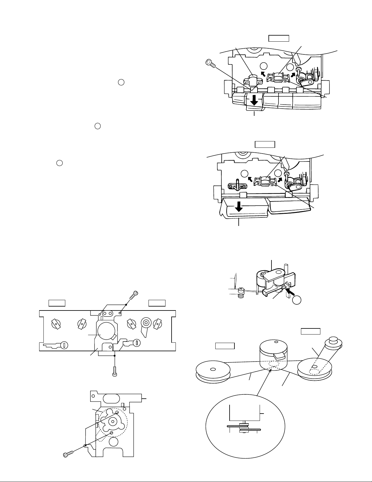
How to remove the pickup (See Fig. 8-1.)
1. Remove the screws (A1) x2 pcs., to remove the shaft (A2) x
1 pc.
2. Remove the stop washer (A3) x1 pc., to remove the gear
(A4) x 1 pc.
3. Remove the pickup.
Pickup
CD Mechanism
Stop Washer
(A3) x1
Gear
Shaft
(A4) x1
(A2) x1
Figure 8-1
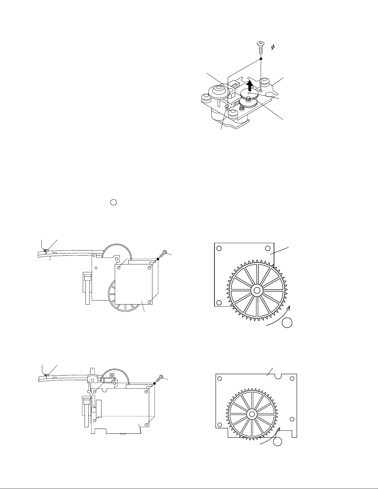
FITTING OF DIAL POINTER
1. Remove the three screws, and remove the tuner PWB from the tuner frame. (See Fig. 8-2) [GX-CH170X]
1. Remove the four screws, and remove the tuner PWB from the tuner frame. (See Fig. 8-2) [GX-CH170Z]
2. Turn fully the dial wheel in the direction. (See Fig. 8-3)
3. Set the dial pointer as shown in Figure 9-2, and mount the tuner PWB.
(GX-CH170X)
A
"0" Point
Tuner
Frame
(GX-CH170Z)
"0" Point
Dial
Pointer
( 235 )
Dial
Pointer
( 235 )
Tuner PWB
(Top view)
Screw x3
Screw x4
Tuner PWB
(Bottom view)
A
Tuner PWB
(Bottom view)
Tuner PWB
(Top view)
Figure 8-2 Figure 8-3
– 8 –
A
Page 9
MECHANISM SECTION
• Driving Force Check
Torque Meter
PLAY: TW-2412 Tape 1: Over 50 g
Tape 2: Over 100 g
• Torque Check
Torque Meter
Play: TW-2111 30 to 60 g.cm 30 to 60 g.cm
Fast Forward: TW-2231 80 to 135 g.cm
Rewind: TW-2231 80 to 135 g.cm
• Tape Speed
Test Tape
Nomal MTT-111 VR391 3,000 Speaker
speed ± 30 Hz terminal
Adjusting
Parts
TAPE SECTION
Position of each switch or control
Volume control Max
Beat cancel A
Function/Power switch Tape/Off
• Bias Oscillation Check
Beat cancel A: 82 + 10 kHz / -6 kHz
• Erase Current Check
Resistor for measurement: 1 ohm 50 ± 15 mV
• Playback Amplifier Sensitivity Check
Test Tape Specified Value
MTT-118 1.8 V ± 3 dB Speaker Terminal
Pin 13 of IC2 Pin 21 of IC2
FET : 2SK19 or 2SK54
D
G
S
10 kohm
Figure 9-1 VCO FREQUENCY TEST CIRCUIT
(GX-CH170X)
Specified Value
Specified Value
Tape 1
Specified
Value
Tape 2
Instrument
Connection
(Load resistance:
6 ohms)
Specified Value
B: -2 ± 2 kHz -4 -9
C: +3 ± 2 kHz 0 +1.5
Specified Value
Instrument Connection
(Load resistance: 6 ohms)
TO FREQUENCY
COUNTER
ADJUSTMENT
TUNER SECTION
fL: Low-range frequency
fH: High-range frequency
• FM IF/RF
Test Stage
IF T1
Detection T2
Band Coverage 87.4 MHz (fL): L2
Tracking 88.0 MHz (fL): L1
• AM IF/RF
Test Stage
IF T3
AM Band Coverage fL: L4 (510 kHz)
(GX-CH170X) fH: TC4 (1,750 kHz)
MWBand Coverage fL: L5 (510 kHz)
(GX-CH170Z) fH: TC6 (1,650 kHz)
SW1 Band Coverage fL: L4 (2.25 MHz)
(GX-CH170Z) fH:TC4 (7.4 MHz)
SW2 Band Coverage fL: L7 (7.2 MHz)
XZ
(GX-CH170Z) fH: TC8 (22.5 MHz)
AM Tracking 600 kHz: L3
(GX-CH170X) 1,400 kHz: TC3
MW Tracking 600 kHz: L3 (MW)
(GX-CH170Z) 1,400 kHz: TC5
SW1 Tracking 2.6 MHz: L3 (SW1)
(GX-CH170Z) 6.0 MHz: TC3
SW2 Tracking 8.5 MHz: L6
(GX-CH170Z) 19 MHz: TC7
• VCO Frequency
Adjusting Point
VR1 76 kHz ± 200 Hz Pin 13, pin 21 and
Note:
After preparing the test circuit shown in Fig. 9-1, connect the Pin 13,
Pin 21 and ground of the IC2 with the test circuit, and measure the
value. At this time, apply a standard unmodulated signal input and
adjust the VCO.
(GX-CH170Z)
GX-CH170X/CH170Z
Specified
Value/Adjusting Point
108.2 MHz (fH): TC2
108.0 MHz (fH): TC1
Specified
Value/Adjusting Point
Specified
Value
Instrument
Connection
Input: Pin 1 of IC1
Output: Pin 17 of IC2
Iuput: Antenna
Output: Headphones
Socket (Load
resistance: 32 ohms)
Instrument
Connection
Input: Antenna
Output: Pin 19 of IC2
Input: Antenna
Output: Headphones
Socket (Load
resistance: 32 ohms)
Instrument
Connection
ground of IC2
FM
TRACKING
fH
fL
L3
AM BAR ANTENNA
AM TRACKING fL
AM TRACKING
fH
TC3
TC1
FM RF
1
T1
L1
IC1
FM IF
TC4
TC2
L2
L4
FM DET
T3
T2
21
1
AM IF
19
IC2
TC3
TC4
L4
VR1
VCO
SW1 TRACKING fLMW TRACKING fL
SW1 TRACKING fH
MW TRACKING fH
TC5
TC7
L6
L5
L7
TC8
TC6
fH SW2
fL TRACKING
fH SW1 BAND
fL COVERAGE
fL MW BAND
fH COVERAGE
fL SW2 BAND
fH COVERAGE
AM BANDfH
fL
COVERAGE
VCO
VR1
FM BANDfL
fH
COVERAGE
17
13
FM fL
TRACKING fH
FM BAND fH
COVERAGE fL
IC1
T1
FM IF
T3
AM IF
L3
MW/SW1 BAR ANTENNA
1
L1
TC1
TC2
L2
T2
1
21
19
17
FM DET
13
IC2
Figure 9-2 ADJUSTMENT POINTS
– 9 –
Page 10
GX-CH170X/CH170Z
3
CD SECTION
Since this CD system incorporates the following automatic
adjustment function, when the pickup is replaced, it is necessary
to reajust it.
Since this CD unit does not need adjustment, the combination
of PWB and laser pickup unit is not restricted.
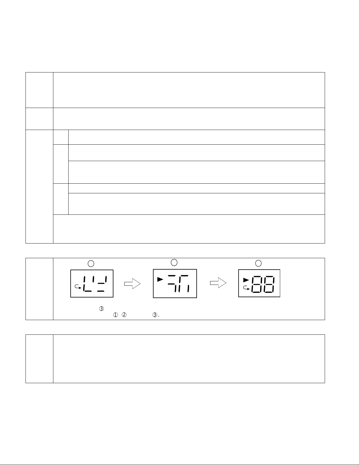
TEST MODE
Start
Note
Operation
After setting the FUNCTION switch to "CD" turn on power. Not later than 1s but later than 500 msec after power is
turned on press simultaneously the following buttons.
1. CD TEST mode DISC1/2 + DOWN/REVIEW
2. LCD TEST mode DISC1/2 + UP/CUE
3. ELECTRONIC VOLUME TEST mode DISC1/2 + STOP
1. When the CD LID switch is in the OFF position, the unit will be able to enter the test mode.
However, playback cannot be performed in this mode.
2. The LCD lights wholly.
The use of the "UP/CUE" button will move the pickup to the outermost position.
1
The use of the "DOWN/REVIEW" button will move the pickup to the innermost position.
When the "PLAY" button is pressed, the laser will be lit, and when the "STOP" button is pressed, it will be
2
turned off. Playback will also start and stop when these buttons are pressed.
a. If the "PLAY" button is pressed while in the stop mode, the laser will simply be turned on at first.
b. If the laser is lit and the "PLAY" button is pressed again, playback will start from the current pickup position.
c. If the "STOP" button is pressed, playback will stop. When pressed again, the laser will be turned off.
Turning the tracking servo on or off.3
a. Each time the PAUSE button is pressed during playback, the tracking servo will be turned on or off.
(Note: If the PLAY button is pressed while in the stop mode, the tracking servo will automatically be
turned on.)
When the TEST mode is entered, at first the CD mechanism is shifted to Tray 1 or Tray 2.
The CD mechanism can be shifted by using the DISC1/2 button.
TRAY-1 OPEN/CLOSE button: The Tray1 can be opened and closed.
TRAY-2 OPEN/CLOSE button: The Tray2 can be opened and closed.
LCD MODE
Display
* After the number 3 has appeared in the display, each time the "UP/CUE" button is pressed, the display will switch
in the following order: 1, 2, and then 3.
1
ELECTRONIC VOLUME TEST MODE
Operation
VOL is set to -14 dB (LCD indication "5").
The VOL setting is changed as follows by using the "VOL UP" button or "VOL DOWN" button.
VOL UP button: VOL setting Min VOL setting -14 dB VOL setting Max
LCD indication "0" LCD indication "5" LCD indication "10"
VOL DOWN button: VOL setting Max VOL setting -14 dB VOL setting Min
LCD indication "10" LCD indication "5" LCD indication "0"
2
1 second1 second
‘
‘
‘
‘
– 10 –
Page 11
GX-CH170X/CH170Z
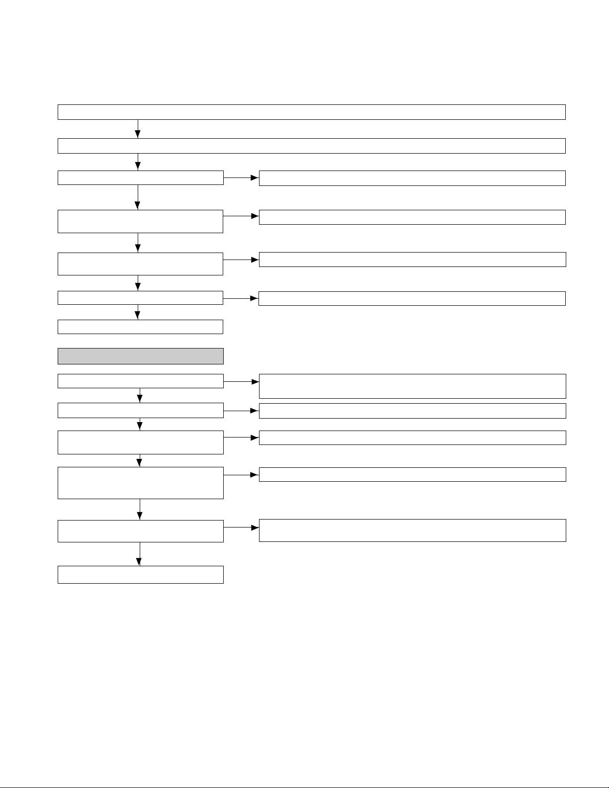
TROUBLESHOOTING (CHANGER CONTROL SECTION)
When the changer mechanism fails to operate normally.
Operation failure may be caused by blocking of disc at the changer mechanism tray. Therefore, it is necessary to check at
first to see whether there is any disc blocking.
If no abnormal phenomena were found and the normal operation cannot be resumed, check as follows.
Set the FUNCTION switch to REMOTE ON mode, and set the POWER button to ON.
Set the FUNCTION switch to CD.
Does LCD give an indication?
Yes
Is the tray opened when the OPEN/CLOSE
button is pressed?
Yes
Does the CD mechanism move up and stop
when disc is selected?
Yes
Is "Er" displayed after normal stop?
No
Normal
• CD microcomputer operation failure.
Is +5V applied to the pin 7 of FW751?
Yes
Is +5V applied to the pin 25 (VDD) of IC901?
Yes
Is the oscillation circuit (periphery of XL701)
of IC901 normal?
Yes
Does LCD display appears when the pin 21
(RESET) of IC901 is instantaneously
connected to GND
Check as stated in item "CD MICROCOMPUTER OPERATION FAILURE".
No
Check as stated in item "THE DISC TRAY CANNOT BE OPENED AND CLOSED".
No
Check as stated in item "DISC CHANGE FAILURE".
No
Check the optical pickup IN switch. (SW702)
Yes
Check for contact failure of Flexible wire. If OK, check the main PWB side power
No
line.
Check the pattern between FW751 and the pin 25 of IC901.
No
XL701 or IC901 is faulty.
No
Check the reset line.
No
Yes
Does the LCD indication change in the LCD
TEST mode?
Yes
Normal
Check voltage on the pins 41, 42, 43, and 44 of IC901. If OK, IC951 or LCD801 is
No
faulty.
– 11 –
Page 12
GX-CH170X/CH170Z
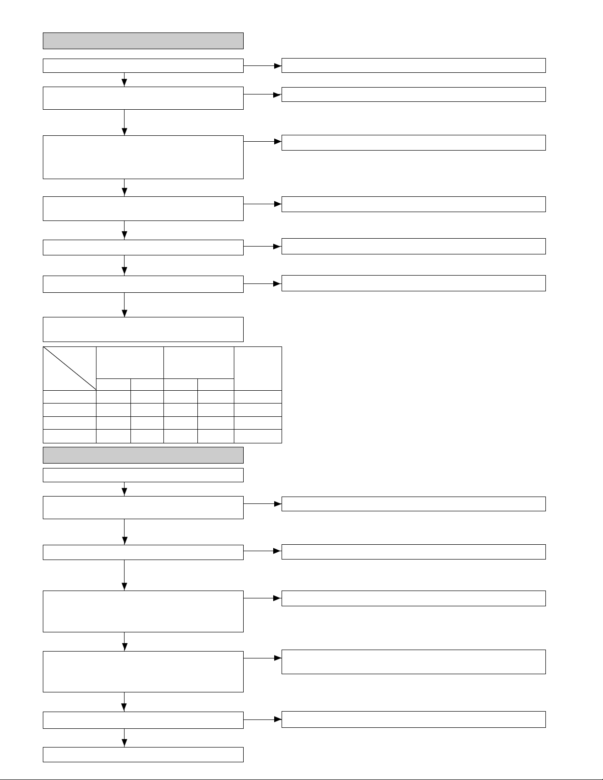
• The disc tray cannot be opened and closed.
Is +7.4V applied to the pin 6 of IC761?
Yes
Does the LCD "?" indication rotate when the main unit
or remote control OPEN/CLOSE button is pressed?
Yes
Check that the pin 64 of IC901 is in Low state but the pin
1 is in High state when the OPEN/CLOSE button is
pressed. (Tray 1 unloading) (Tray 2 unloading: Pin 64
High, pin 1 Low)
Yes
Check that +6V is output to the pin 9 in Tray1 mode and
that +6V is output to the pin 7 in Tray2 mode.
Yes
Is about +6V output between pins 4 and 5 of CNP753?
Yes
Is about +6V applied to the loading motor M981C?
Yes
Check the loading motor M981C and loading
mechanism.
Check the +7.5V power line.
No
Check the main unit button or remote control.
No
Check IC901.
No
IC761 is defective.
No
Check the pattern between IC761 and CNP753.
No
Check for breakage of connecting wire for loading motor M981C.
No
IC901 IC761
Pin 1 Pin64 Pin 7
Tray1 Open H L 0 +6V Reverse
Tray2 Open L H +6V 0 Forward
Tray1 Close L H +6V 0 Forward
Tray2 Close H L 0 +6V Reverse
Pin 9
M981C
Motor
operation
• Disc change failure.
Is +7.4V applied to the pin 6 of IC761?
Does the LCD "?" indication rotate when the main unit
or remote control DISC CHANGE button is pressed?
Yes
Disc move failure?
Operation
failure
Check that the IC901 pin voltage is as follows:
Pin 1 Pin 64
Disc2 -> Disc1 L H
Disc1 -> Disc2 H L
Yes
No
Remains
persistently.
No
Check the main unit button or remote control.
Check the changer mechanism switches.
IC901 is defective.
Check that the IC761 pin voltage is as follows:
Pin 7 Pin 9
Disc1 -> Disc2 0 +6V
Disc2 -> Disc1 +6V 0
Yes
Is voltage applied to the loading motor M781C?
Yes
The motor M981C is defective.
IC761 is defective. Or check the pattern between pin 64 of IC901 and
No
pin 1 of IC761, the pattern between pin 1 of IC901 and pin 3 of IC761.
Check for breakage of wire CNW753 to loading motor M981C.
No
– 12 –
Page 13
GX-CH170X/CH170Z
TROUBLESHOOTING (CD SECTION)
When the CD does not function
When the CD section does not operate When the objective lens of the optical pickup is dirty,this section may not operate.Clean
the objective lens,and check the playback operation.When this section does not operate even after the above step is taken,check
the following items.
Remove the cabinet and follow the troubleshooting instructions.
"Track skipping and/or no TOC(Table Of Contents) may be caused by build up of dust other foreign matter on the laser pickup lens.
Before attempting any adjustment make certain that the lens is clean. If not, clean it as mentioned below."
Turn the power off.
Gently clean the lens with a lens cleaning tissue and a small amount of isopropyl alcohol.
Do not touch the lens with the bare hand.
• The CD function will not work.
The CD operating keys don't work.
Yes
Check the CD, DPS microcomputer (IC701), power supply, 4.0
MHz and 16.93 MHz clock, and reset terminal.
Yes
Check the waveform of SCK, SO (DATA) and SI (COMM).
Yes
See if the pick-up is in the pick-up in SW4 position.
Yes
If the items mentioned above are OK, check the main
microcomputer IC901.
• The CD operating keys work.
Check the Focus - HF system.
When the PLAY button is pressed without first loading a disc,
does the pickup go up and down?
Yes
Does the pick-up move up and down twice?
No
Does the output waveform of IC801(16)(FD) match that shown in
Fig. 13?
No
Check the IC801(50)(CLK) line, 4MHz.
Check the microcomputer data on pins (51)(CL), (52)(DAT) and
(53)CE.
Yes
Yes
0.5s
0.50 V
IC801 16 FD
0.5s
0.50 V
IC801 15 TD
Focus search OK.
Check the area around IC804-BI801/CNS801.
Focus search
is performed
two times
when play
operation is
done without
disc.
– 13 –
1
2
Figure 13
Page 14
GX-CH170X/CH170Z
• Playback can only be performed when a disc
is loaded.
Is the Focus servo active? (Can you hear it working?)
Yes
Does the DRF signal change from "L" to "H"?
Yes
Is HF waveform normal (see the Fig.14-1, 2)?
Yes
Check the tracking system.
HF
0.1V/DIV
0.5µsec/DIV(DC)
(When playing
back the disc)
No
No
No
0.5s
1.00 V
IC801 16 FD
0.5s
10.0 V
IC801 12 CLV+
0.5s
10.0 V
IC801 54 DRF
0.5s
2.00 V
IC801 7 TE
Check the laser diode driver.
Check the area around IC801(16) - (21) (focus servo circuit).
Yes
If the disc is not turning, the DRF
should not change to "H".
Check the spin
system.
Yes
Level is abnormal.
Check the periphery
of IC801 pins 41 and
42.
Yes
Waveform is unstable.
Check the spin
system.
Waveform in case
of normal playback
2
1
3
4
Figure 14-1
• Check the tracking system.
Check waveform of IC801 pin 7 (TE).
The waveform shown in Fig. 14-3
appears, and no-disc state appears
soon.
Play is possible in
TEST mode.
Data cannot be read.
Yes
Although IL is possible,
play is impossible.
Yes
5ms
1.00 V
IC801 7 TE
Yes
Tracking servo is inoperative.
Normal jump is impeded, and the
program top cannot be reached.
Yes
Check the VCO-PLL system.
Figure 14-2
Yes
4
Check the periphery of IC801
pin 8 to pin 15, and IC804 to
BI801/CNS801.
Check the periphery of
IC801 pin 14.
Yes
5 ms
5.0 V
IC801 54 DRF
3
Figure 14-3
– 14 –
Page 15
• Checking the spin system.
Play operation is performed without disc.
Yes
GX-CH170X/CH170Z
The turntable rotates a little.
No
The turntable fails to rotate or rotates at high speed.
• Checking the VCO-PLL system
Play operation is performed when disc exits.
Yes
Although HF waveform is normal, TOC data cannot be read.
Stop --> Play
As VCO freque-
0.5s
1.00 V
IC802 3 PDO
0.5s
1.00 V
IC801 16 FD
ncy is locked at
4.32 M Hz,
voltage of PDO
2
rises and stabilizes.
Yes
Yes
Yes
The spin driver circuit is normal.
Check the periphery of IC801 pins 23 to 27, pin 39 and pin 40,
IC802 pin 12 and pin 13, IC804 to BI803/CNS803.
Check PDO waveform (Fig. 15).
Error
Check the IC801 pins 43 and 44, IC802 pins 3, 5, 7, 9 and 10.
3
Figure 15
• Although HF waveform is normal and the time
indication is normal, no sound is emitted.
Check IC802 pin 48 (EFLG).
Yes
Check IC802 pins 37and 40.
Abnomal
Check the periphery of IC803 (OPAMP).
No
Usually, the number of pulses of flawless disc is 100 pulses/
sec or less.
– 15 –
Page 16
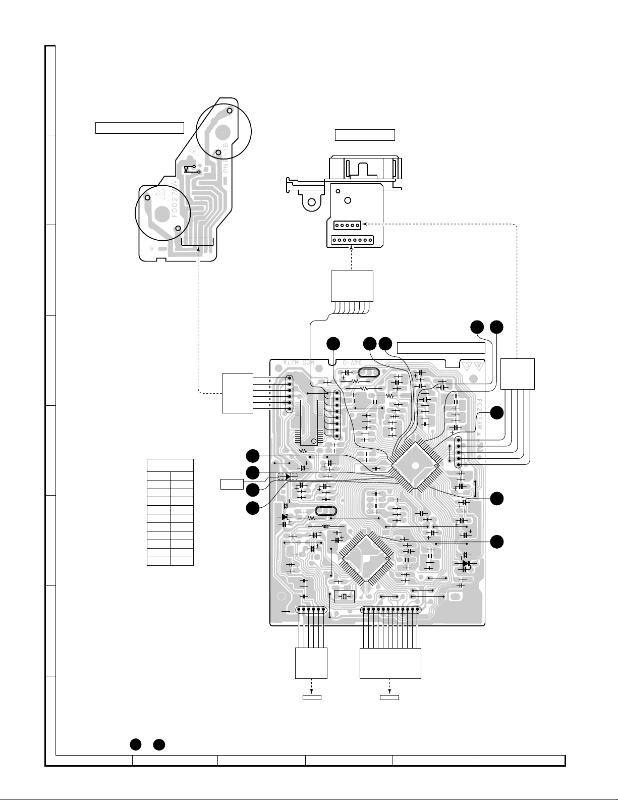
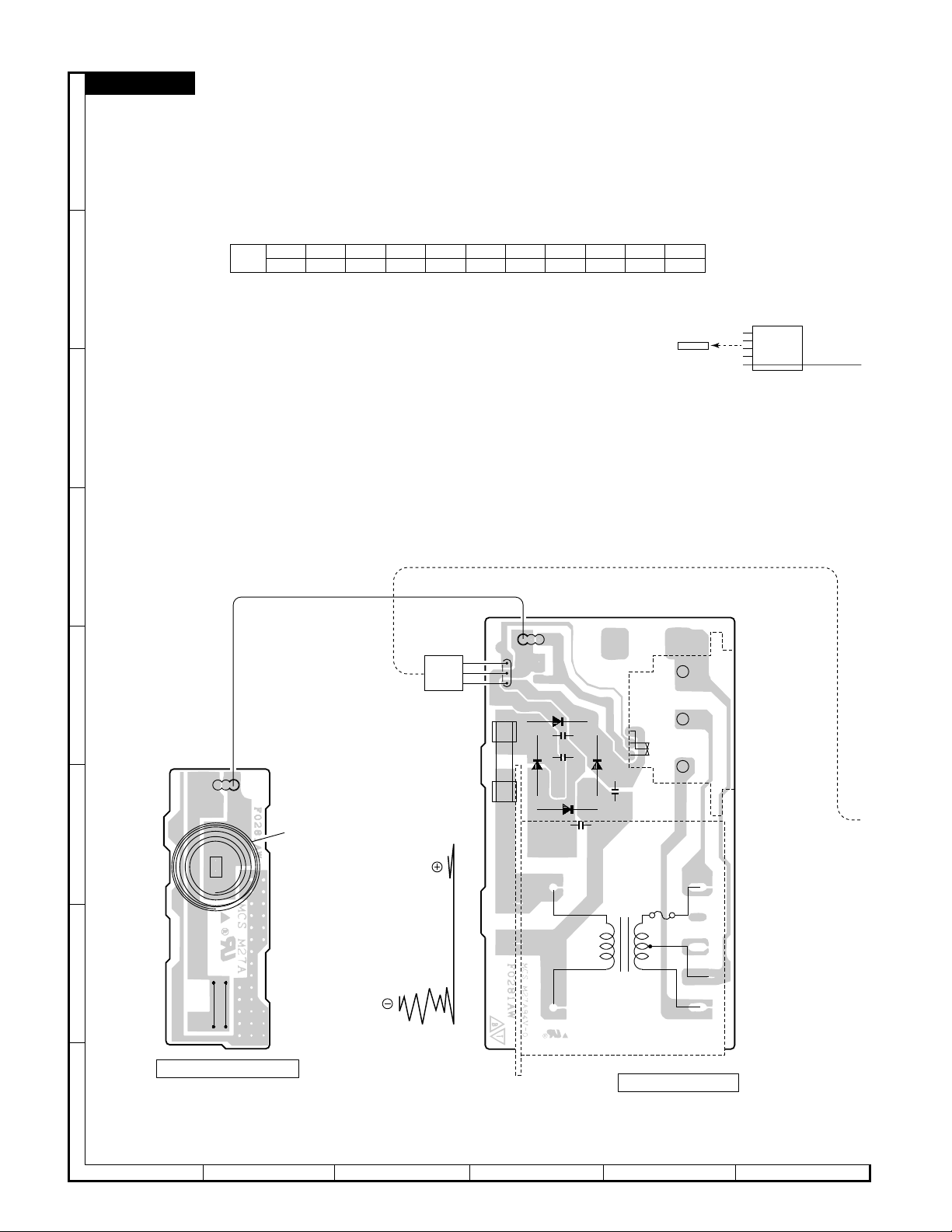
GX-CH170X/CH170Z
NOTES ON SCHEMATIC DIAGRAM
• Resistor:
To differentiate the units of resistors, the symbol as K and M
are used: the symbol K means 1000 ohm and the symbol M
means 1000 kohm and the resistor without any symbol is an
ohm resistor. The resistor designated "Fusible" is a fuse type
resistor
• Capacitor:
To indicate the unit of capacitor, a symbol P is used: this
symbol P means micro-micro-farad and the unit of the capacitor
without such a symbol is microfarad. As to electrolytic capacitor,
the expression “capacitance/withstand voltage” is used.
(CH), (TH), (RH), (UJ): Temperature compensation
(ML): Mylar type
(P.P.): Polypropylene type
• The indicated voltage in each section is the one measured by
Digital Multimeter between such a section and the chassis
with no signal given.
REF. NO DESCRIPTION POSITION
SW1 BAND [GX-CH170Z ONLY] FM—SW2—SW1
—MW
SW4 PICKUP IN ON—OFF
SW201 RECODE/PLAYBACK R—P
SW251 DUBBING SPEED/BEAT CANCEL NORMAL A—
NORMAL B—
HIGH C/A—B—C
SW253 BAND [GX-CH170X] FM—AM
SW253 TAPE SELECTOR/FM MODE NORMAL—CrO2/
[GX-CH170Z] FM STEREO—
FM MONO
SW601 TAPE 1 MAIN ON—OFF
SW602 TAPE 2 MAIN ON—OFF
SW603 TAPE1/2 SELECTOR ON—OFF
SW651 FUNCTION/REMOTO CONTROL CD—TUNER—
TAPE—OFF/
ON—OFF
SW701 POWER ON—OFF
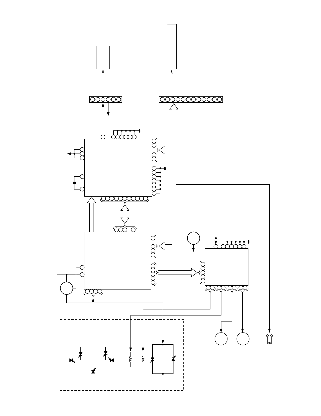
1. Tuner
( ): AM mode
Marking except for ( ): FM mode
2. CD
( ): Play mode
Marking except for ( ): Stop state
3. Deck section
( ): Record mode
Marking except for ( ): Playback mode
Display / Control section:
( ): Active state
Marking except for ( ): CD Function mode at stop state
• Schematic diagram and Wiring Side of P.W.Board for this
model are subject to change for improvement without prior
notice.
• Parts marked with “ ” ( ) are important for
maintaining the safety of the set. Be sure to replace these
parts with specified ones for maintaining the safety and
performance of the set.
REF. NO DESCRIPTION POSITION
SW702 CD-STOP ON—OFF
SW703 CD-PLAY ON—OFF
SW704 CD-PAUSE ON—OFF
SW705 CD-CUE ON—OFF
SW706 CD-REVIEW ON—OFF
SW707 CD-DISC 1-2 ON—OFF
SW708 CD-RANDOM ON—OFF
SW709 VOLUME UP ON—OFF
SW710 VOLUME DOWN ON—OFF
SW711 CD-PROGRAM ON—OFF
SW712 CD-CLEAR ON—OFF
SW713 CD-TRAY1 OPEN/CLOSE ON—OFF
SW714 CD-TRAY2 OPEN/CLOSE ON—OFF
SW981 TRAY/MECHANISM UP ON—OFF
SW982 TRAY1 1a—1b
SW983 TRAY2 2a—2b
FRONT
VIEW
ECB
(S)(G)(D)
(1) (2) (3)
2SC2001 K
2SB561 C
2SB562 C
2SD468 C
KRA102 M
KRC102 M
KTA1266 GR
KTC3199 GR
FRONT
VIEW
FRONT
VIEW
BCE
2SD2394 F
Figure 16 TYPES OF TRANSISTOR AND LED
3N4PDN32
3N4GDN32
– 16 –
FRONT
VIEW
GREEN
3N8PGN33
2
3
1
RED
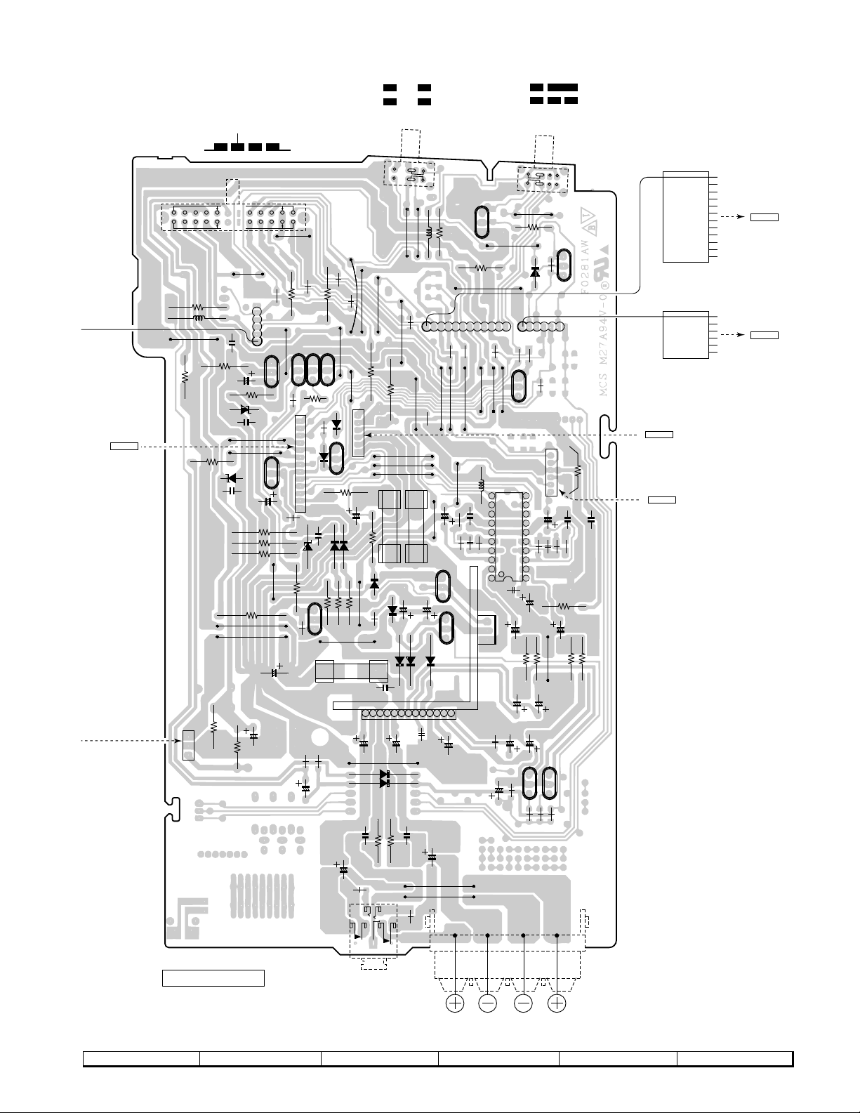
Page 17
GX-CH170X/CH170Z
1
2
3
4
5
6
7
8
9
10
11
12
1
2
3
4
5
6
37
33
32
11
4
2
43
22
6
4544
444340
9
10
12
131415
16
17
18
19
20
1
53
38
39
51
62 64
6158
63
32
64 62
123
4
30
49
54
15 16
27
28 29
3
10
19
23 25
22
5
6
7
8
13
28
11
12
1
2
17
18
26
27
8
46
31
+5V
FOCUS COIL
TRACKING COIL
PICKUP UNIT
MOTOR
SPIN
SQOUT
PUIN
RES
COIN
CQCK
RWC
SL+
SL–
DRF
WRQ
CNS852
GND(A)
R-CH
L-CH
+7.4V
GND(D)
CNS851
GND(P)
TO
MAIN
SECTION
+7.4V
(CD)
LCHO
XVDD
VVDD
VDD
XIN
XOUT
~
EFMO
EFMIN
CLV+
CLV–
V/P
HFL
TES
TOFF
TGL
JP+
JP–
~
IC802
LC78622E
SERVO/SIGNAL
CONTROL
SLI
SLC
CV+
JP–
Q805
+5V
FIN1EF
LDO
VCC1
FIN2
~
FD
SPO
SLEO
SLD
/THLD
DEF
SL+
SL–
DRF
TO
CL, DAT, SELIAL CONTROL
+7.4V
Q804+5V
M
M701
SW702
PICKUP IN
DRIVER
LASER
M
M702
SLIDE
MOTOR
IC801
LA9240M
SERVO AMP.
CD-GND
DEF1,4MCLK,
RES,CQCK,
COIN,SQOUT,
RWC,WRQ
16.93MHz
XL801
FOCUS/TRACKING
/SPIN/SLIDE
DRIVER
IC804
BA5920FP
CD 5V
TO
MICROCOMPUTER
Figure 17 BLOCK DIAGRAM (1/3)
– 17 –
Page 18
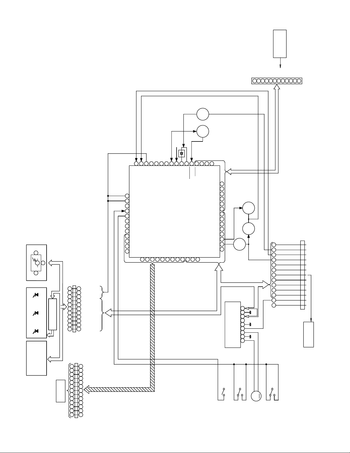
GX-CH170X/CH170Z
3
12
3
21
98
7
6
5
4
3
2
1
13121110
13121110
98
7
6
5
4
1
2
3
4
5
6
7
8
9
10 11 12 13
14
17
18
19
20
21
22
23
24
25
26
27
28
29
30
31
32
41
4243
44
53
54
55
6
5
5
7
5859
6
0
1
6
33
3435
36
37
38
39
40
6
2
6463
98
7
6
5
4
3
2
1
1
10
9
8
7
6
5
4
3
2
11
12
7
98 6
5
4
3
21
1
7
98 6
5
4
3
2
2
3
4
5
6
7
89
10 11
1
101110
11
12 13
LED704LED703LED701
POWER TRY-2TRY-1
KEY1
KEY2
TRY1 LED
TRY2 LED
PWR-IN
VREF
GND
FW702
POWER-CD-VOL
OPERATION KEY
SW701 ~ SW714
REMOTE SENSOR
RX701
FW701
LED CONTROL
Q711 ~ Q715
VSS
Q704Q702
RESET
BEAT
µ-COM5V
COM3
COM2
COM1
COM0
SEG7
SEG8
SEG
SEG
SEG
SEG
SEG
SEG
SEG
VLC2
VLC1
VLC3
KEY1
KEY2
UP-SW
TRAY SW
MODEL
CD/SYC-IN
AC/DC
REMOCON
VREF
AVSS
XC-IN
XC-O
VDD
VSS
X-OUT
X-IN
PU-IN
WRQ
SQ-OUT
DRF
RESET
MTR2
PWR-IN
DATA(VOL)
STB(VOL)
MUTE
SYC-OUT
RES
CQCK
C0IN
RWC
SL+
SL–
CK(VOL)
PWR-0N
TR1 LED
TR2 LED
MTR1
Q705
Q701
Q703
AC-ON
PLUS
POWER
PUIN
WRQ
COIN
CQCK
RES
CD5V
CD-GND
DRF
SL–
SL+
RWC
SQOUT
FROM
CD-SERVO
SECTION
+
–
M
SW981
TRAY/
MECHANISM UP
TRAY2
SW983
M981
LOADING
MOTOR
SW982
TRAY1
REMOCON
CH7.4V
P-GND
VOL(STB)
VOL(CK)
VOL(DATA)
GND
MUTE
POW-ON
CD/SYC-IN
TWEET CANCEL
FW751
TO MAIN
SECTION
X701
4MHz
IC901
IX0146AW
SYSTEM
MICROCOMPUTER
BA6218
IC761
CHANGER
MOTOR CONTROL
µ-COM5V
AC-ON
µ-COM5V
LCD801
CD LCD
CANCEL
PWR-ON
AC-ON HI
SY OUT
Figure 18 BLOCK DIAGRAM (2/3)
– 18 –
Page 19

GX-CH170X/CH170Z
1
5
20
1
7
48
6
9
5
32
4
12
8
19
18
9
10
21
7
14
15
13
1116
17
32
22
23
15
12
13
9
19
1
24
7
18
19
11
8
5
12
10
6
2
19
2
18
3
20
7
24
254
3
1
6
11 12 13
12
3
4
5
6
7
89
10 11 12
21
4
23
2
13
6
1
3
CF2
10.7MHz
CF3
AM IF
T1
FM IF
P. B
REC
REC/PB
REC/PB
HEAD
L-CH
R-CH
T3
P. B
FM DET
T2
L2
FM OSC
FM
+B
L1
FM RF
ERASE
HEAD
REC
RF
REG.
MPX
OSC
AGC
DET.
AM-IF
LEVEL-DET.
FM-IF
DET.
AMP.
POST
MUTE
DRIV.
TU
DECODER
DET.
PHASE
VCO
FF FF
PILOT
DET.
ST.
DRIV.
FF
ST.
SWIT.
TRIG.
VCC
ROD ANTENNA
L
R
R
L
R
L
SW201
P. B
L-CH
R-CH
REC
T1/T2
T1/T2
TUNER
+B
R
L
+B1
P. B
455kHz AM
+B2
AC INPUT
T651
POWER
TRANSFORMER
VR1
VCO
MONO
T2 PB HEAD
T1
L(T2)
R(T2)
L(T1)
R(T1)
WOOFER
WOOFER
Q623
CNP601
SP602
D651 ~ D654
RECTIFIER
MUTING
VR391
M601
TAPE
MOTOR
REC
R-CH
AUDIO
L-CH
CD+7.3V
POWER
GND
GND
CD
BATTERY
DC 12V
AC ON
SW201-B
REC/PB
SW201-A
REC/PB
+
+
–
–
J601
HEADPHONES
TWEETER
SP603
L-CH
SP601
SP604
TWEETER
R-CH
SPEAKERS
Q651
Q657
Q653
µ-COM+5V
Q654
Q652
POWER ON
SWITCHING
SWITCHING
POWER-ON
+12V
Q658
Q659
POWER
VOLTAGE
REGULATOR
+B1
REGULATOR
VOLTAGE
7.4V
FUNCTION
POWER/
REGULATOR
VOLTAGE
SWITCHING
CD/SYNC-IN
SYNC-IN
Q656
Q655
Q662
STAND-BY
LA4597
IC601
MUTING
Q521
Q522
MUTE
DRIVER
TUNER +B
AUDIO +B
SW651-B
CANCEL
SW251-B
SW651-B
FUNCTION
FM +B
TO µ-COM
SECTION
P-GND
CH7.4V
GND
MUTE
POW-ON
AC-ON
CD / SYC-IN
TWEET CANCEL
13
SYC-OUT
VOL(CK)
VOL(STB)
VOL(DATA)
Q202
Q201
FUNCTION
SW651-C, D
RADIO
Q660
DUBBING
SWITCHING
Q393
Q394
SWITCHING
M
TAPE SPEED
Q392
Q391
Q252
BIAS
OSC.
Q351
L351
C, D, E, F
SELECTOR
SW607
CNP851
TO CD SERVO
SECTION
F1
B. P. F
FM FRONT END
LA1186N
IC1
IC2
LA1805
FM/AM IF MPX.
TAPE
ELECTRONIC
VOLUME
IC500
TC9211P
POWER AMP.
[ "D" size ( UM/SUM-1,
R20 or HP-2 ) battery x 8]
SW601 T1 MAIN
SW602 T2 MAIN
DUBBING
SW251
SPEED/
BEAT
CANCEL
TWEET
IC201
AN7345K
PLAYBACK AND
RECORD/PLAYBACK
AMP.
µ-COM5V
SO651
FOR Z
FOR X
X : AC 220-240V
50Hz
Z : AC 110-127
/220-240V
50/60Hz
SW651-A
FUNCTION
POWER-ON
12V
TAPE +B
X ONLY
TAPE +B
MOTOR-CONT
SELECTOR
TAPE
SW253-B
Z ONLY
Q352
Q353
Q362
Q363
X ONLY
Z ONLY
F661
T500mA
L 250V
TUNER +B
TUNER +B
SW253-A
Z ONLY
SW253
X : BAND
Z : TAPE
SELECTOR
GND
AM OSC.
L5
L7
SW2 OSC.
L4
SW1 OSC.MW OSC.
BAND
SW1-E
FOR Z
L4
FOR X
CNP751
F662
T500mA
L 250V
8KHz
VR904
A, B
1KHz
VR903
A, B
125Hz
VR902
A, B
Q901
Q902
EQUALIZER
GRAPHIC
X-BASS
A, B
VR901
AM BAR ANT.
L3
FOR X
SW1-C
BAND
BAR ANT.
MW/SW1
L3
FOR X
RF AMP.
MIX OSC
VCC
F1
B.P.F
ROD ANTENNA
L6
SW2 ANT.
BAND
SW1-A
FOR Z
FOR Z
X : GX-CH170X
Z : GX-CH170Z
F651
T2.5A
L 250V
F663
T1.25A
L 250V
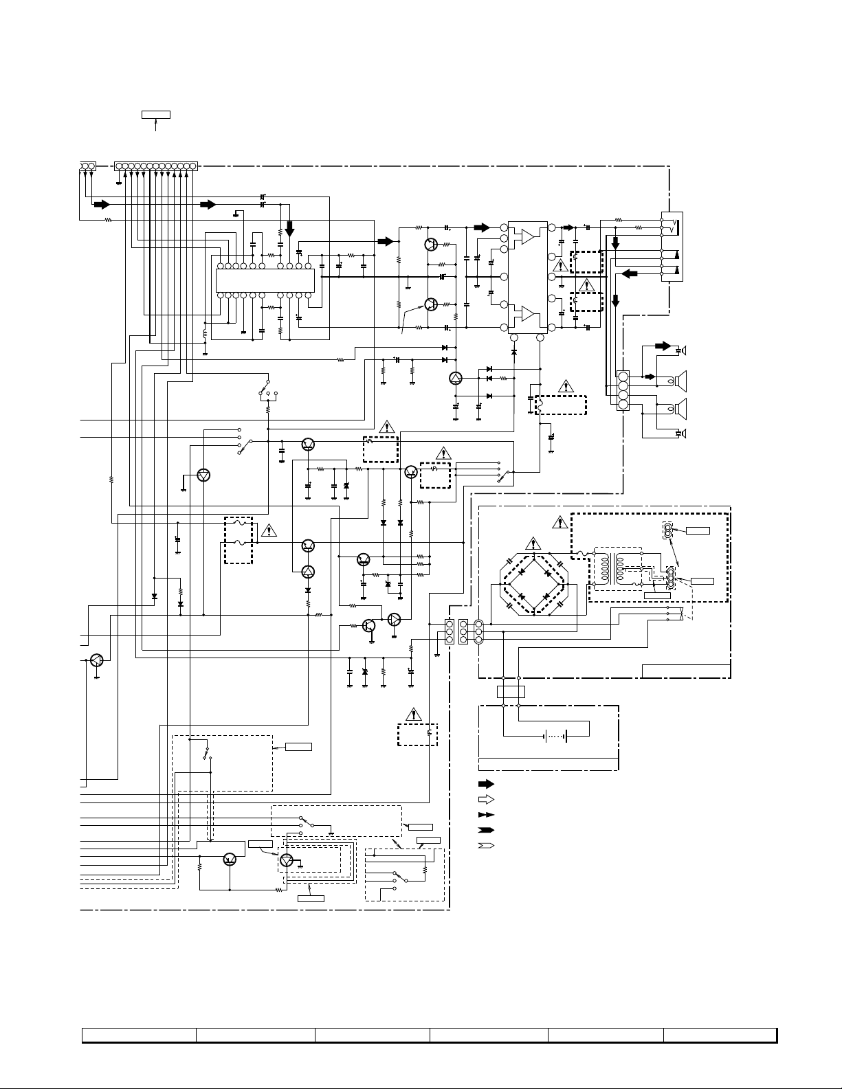
Figure 19 BLOCK DIAGRAM (3/3)
– 19 –
Page 20
GX-CH170X/CH170Z
A
CD MOTOR PWB-E
B
+
M702
SLIDE MOTOR
M701
SPIN MOTOR
SW702
PICKUP IN
-
CNP803
-
PICKUP UNIT
+
654321
C
CNS801
23456781
RDWHGYWHGYWHGY
WH
1 8
7 12 10
R822
R880
R823
C817
33
R842
R839
R840
32
35
XL801
C848
BI801
Q804
C873
Q805
BCE
R829
C849
R819
C815
R820
R821
C816
R826
R827
C822
C830
R833
C832
R832
16
17
15
20
25
30
IC802
40
45
50
49
48
D
CNS803
1
WH
2
GY
3
WH
4
GY
5
WH
6
CNS803
15212228
R810
14
16
RD
IC804
18
R878
R877
CNP851
C867
C868
C869
R875
C887
178
BCE
L801
C843
C819
R831
C820
C846
C870
R876
ZD801
R873
R830
C844
C818
R824
R825
C889
R874
E
COLOR TABLE
BR
BROWN
RD(R)
RED
OR
ORANGE
YL
YELLOW
GR
GREEN
BL
BLUE
VL
VIOLET
GY
F
WH(W)
BK
PK
GRAY
WHITE
BLACK
PINK
X:JUMPER
Z:D803
6
5
4
3
CD SERVO PWB-D
C807
R812
C813
R813
R828
R814
C811
R815
C814
R816
C812
1720
R817
15
25
32
30
35
IC801
33
40
45
50
48
R834
C850
R837
R835
C831
R856
10
55
5
CNP852
R857
C842
164
C841
60
R858
C847
R860
CNS802
R805
R806
C809
C806
R807
C804
C808
R809
R811
R808
C810
16
10
5
60
55
49
C805
R804
R802
R803
C803
BI802
164
15
C801
R801
C802
C840
R871
R836
C833
R838
C834
C845
C835
C851
C839
R849
C838
D802
C837
C821
9
RD
WH
GY
WH
GY
2
11
12345
G
CNS851 CNS852
H
The numbers 1 to 12 are waveform numbers shown in page 35.
1
2
34 5
Figure 20 WIRING OF P.W.BOARD (1/8)
BLGRYLORRD
CNP851
P25 11 - C [X]
P27 11 - C [Z]
TO MAINN PWB
– 20 –
BR
123456
GYBKGYBKGYBKGYBKGYBKGY
CNP852
P30 5 - B
TO DISP PWB
RD
123456789101112
6
Page 21
GX-CH170X
GX-CH170X/CH170Z
(211)
TUNER PWB-B
GX-CH170Z
CNS2
CNS3
2
1
2
1
P26 5 - C
FW1
TO MAIN PWB
CNP1
12345
T1
P24 5 - C
FW1
TO MAIN PWB
CNP1
C34
C33
6
5
T3
4
3
2
1
C21
R3
R25
C17
R7
T1
C2
3
2
F1
1
C31
CF3
1123
C26
C15
R9
C10
C32
C20
23
IC1
1
IC2
12
10
C24
C22
5
C39
1
CF2
9
R5
8
7
6
5
4
R1
3
2
C16
C27
C28
13
15
20
24
C37
C14
C5
C8
R2
C9
L1
R29
C25
R30
R27
C23
R26
R6
C29
L2
C6
C4
VC1 VC2
C35
VCO
VR1
T2
C38
C11C36
TC2TC1
VC3 VC4
L3
AM BAR ANTENNA
R35
CNW2
L4
TC4TC3
ROD ANNTENA
(210)
BK
4
VR500
1
FINE
BI500
TUNING
LED500
FINE TUNING PWB-A9
TUNER PWB-B
SW2
SW1
MW
FM
SW1
BAND
(211)
CNW2
ROD ANNTENA
(210)
C33
C32
89
7
6
5
4
3
12
2
1
1
89
6
4
3
12
C28
IC2
31
1
1
C25
4
01
5
1
6
R27
C24
1
7
1
8
7
C23
1
9
1
0
5
C22
2
R26
1
2
C39
2223
R6
24
C37
CF2
C14
C8C5C6
R5
R2
C9
R1
C4
L1
D1
C34
CNP3
R36
C31
CF3
123
T3
C26
C21
C17
C20
123
R3
R25
C15
R7
R9
C10
C2
IC1
3
F1
12
MW
MW/SW1 BAR ANTENNA
C35
C27
T2
C29
L2
VC1 VC2
C16
R35
VCO
VR1
R29
R30
R28
L7
C38
L4
C11
TC2TC1
TC4
C42
TC3
VC3 VC4
C41
SW1
L3
TC6
C48
TC5
TC8
C50
R40
C49
C46
C56
R42
F
E
SW1
L5
C55
R50
C
C40
CNP2
C51 C44
D
L6
B
A
TC7
CNW3
78 9101112
Figure 21 WIRING OF P.W.BOARD (2/8)
– 21 –
Page 22

GX-CH170X/CH170Z
A
CD SERVO PWB-D
A
B
C804
0.001
C
C807
0.1/50
R807
1K
D
E
C811
0.1
C803
0.1/50
TE
R809
27K
R811
3.3K
R840
22K
R805
6.8K
R828
R839
22K
R804
2.2K
1K
R806
100
R802
100K
C809
0.047
R808
12K
C806
0.033
C805
0.033
C808
0.068
R803
R829
1K
LASER DRIVER
Q805
R842
22
C848
1/50
KTA1266 GR
C849
0.022
+B
C840
0.33/50
C838
0.01
1/50
C839
6061626364
BHI
1
2
FIN1
E
3
F
4
5
R813
33K
C813
0.1
TB
TE–
6
TE
7
8
TES1
REF
9
SCI
TH
10
TA
11
12
TD–
TD
13
14
–
+
TO
15
16
FD
15K
C810
180P
R812
15K
+
–
REF
+
REF
–
+
VCR
–
REF
+
VCR
–
+
REF
BAL
+
–
REF
HIST. COMP
SHOCK; WCOMP
REF
+
–
REF
+
GEN
–
TO
REF
REF
+
GEN
–
REF
+
–
FD–
FA
1817 19 2320 21 22 24 25 26 27 30 31 3228 29
R814
10K
R815
47K
LDS
–
VCC1
FIN2
VREF
PHI
LDO
RF
–
FE1
+
REF
VCR
–
VCR
+
SERVO AMP.
+
–
+
TGL1
–
REF
GL
THDL
THD
WCOMP
JP
FSC
GEN
REF
REF
+
–
–
+
FOF
FE
FE–
SP
C812
330P
R817
82K
R816
1.5K
AGND
R819
39K
FA–
C814
0.01
GND
C837
10/16
VR
LF2
REFI
+
–
REF
+
DEF
–
–
HFL
+
+
DRF
–
IC801
LA9240M
VCC
+
–
+
–
PSTR
S.Q.R
+
–
REF
+–
SPOF
SPGJPSPI
REF
10K
R820
R823
C815
0.0047
1.2K
C817
0.47/50
REF
REF
JP
SP–
C816
0.001
R821
56K
R822
6.8K
C835
VCC
0.1/50
VCC2
+
–
+
–
SPO
R830
FSS
R824
1K
FEBAL
FOSTA
TOSTA
2FREQ
LASER
FSTA
8/12CM
SLOF
REF
10K
R871
4.7K
4950515253545556575859
NC
48
CL
CE
DRF
JP–
JP+
CV–
CV+
SLOF
OR
SLOF
TO
REF
SLEO
C819
47/10
1/50
C818
R825
DAT
SLOF
SLD
1.2K
REF
+
–
LATCH
P-ON RES
RF
+
–
C820
CLK
CLK
CE
CL
DAT
SL–
0.0033
R831
TBC
47
DEF
THLD
FSC
46
45
DGND
SLI
44
REF
–
+
43
SLC
42
RFS–
+
–
41
RFSM
CV+
40
CV–
39
SLOF
38
HFL
37
36
TES
TOFF
35
TGL
34
JP+
33
JP–
SL+
R827
220K
R810
82K
220K
R826
1K
C833
0.001
C830
2.2P
C845
4.7/50
C834
0.033
R833
5.6K
R832
C850
0.1
R838
33K
R836
R837
47K
47K
R834
C832
1K
27P
56K
C831
R835
0.0027
470
HF
C822
220P
C821
1/50
D802
1SS133
C851
0.022
R849
100K
F
CD SIGNAL
CNS852
BI852
CD 5V
5V
CNS851
CD-GND
PUIN
WRQ
SQOUT
RWC
COIN
CQCK
RES
DRF
SL–
SL+
12
11
10
9
8
7
6
5
4
3
2
1
6
5
4
3
2
1
BI851
DIGITAL GND
PU IN
WRQ
SQOUT
DRF
SL(–)
SL(+)
RWC
CO IN
CQCK
RES
DIGITAL GND
DIGTAL +7.4V
L-CH
AUDIO GND
R-CH
12
11
10
9
P28 8-G
CNP852
TO DISPLAY PWB
G
P28 1-E
CNP851
TO MAIN PWB
8
7
6
5
4
3
2
1
6
5
4
3
2
1
H
The numbers 1 to 12 are waveform numbers shown in page 35.
1
2
34 5
Figure 22 SCHEMATIC DIAGRAM (1/7)
– 22 –
+B
6
Page 23

GX-CH170X/CH170Z
CNS802
1
2
3
4
5
2
3
4
5
6
7
8
1
2
3
4
5
11
2
3
4
5
6
7
8
PICKUP UNIT
K
E
A
B
F
TR–
TR+
FO+
FO–
GND
PD
VR
LD
1M
2200P
1/16
LD
MON
K
E
A
B
F
C
1M
LT0H30M1
2200P
TR+
FO+
FO–
TR–
ACTUATOR
F
E
B
DEFI
TA1
PDO
VVSS
ISET
VVDD
FR
VSS
EFMO
EFMIN
TEST2
CLV+
CLV–
V/P
HFL
TES
A
K
C847
0.01
64 63 62
TEST1
/CS
TEST5
SLICE LEVEL
CONTROL
SERVO
COMMAND
TOFF
17
61
4M
DIGITAL
SERVO
TGL
18
R860
1K
60
16M
VCO CLOCK
CONTROL
CLV
JP+
19
59
58 575655
/RES
TST11
OSC
JP–
PCK
COIN
/CQCK
SQOUT
µ-COM
INTERFACE
2K x 8 BIT
RAM
ERROR
CORRECT
FLAG CONTROL
SYNC-DETECT
EFM DEMODULATE
VDD
CONT1
FSEQ
222120
C802
47/10
54 355251
FSX
RWC
WRQ
EXTERNAL
OUTPUT
CONT2
CONT3
CONT4
CONT5
27
26252423
50
SFSY
SBCK
SUB-CODE
X-TAL
GENERATOR
4FS
DIGITAL
FILTER
C2F
EMPH
2928
R801
1K
49
PW
1BIT
DAC
DIGITAL
OUT
DOUT
3130
EFLG
SBSY
XOUT
XVDD
MUTER
MUTEL
TEST4
XVSS
RVDD
RCHO
RVSS
LVSS
LCHO
LVDD
32
C801
0.01
XIN
NC
TEST3
BI802
K
1
E
2
A
3
B
4
F
5
BI801
TR–
1
TR+
2
FO+
3
FO–
4
GND
5
R876
10K
R875
10K
PD
6
VR
7
LD
8
CNS801
FO+
FO–
TR–
TR+
C870
0.0022
C869
0.0022
+B+B
48
47
46
R880
100
C868
10/16
C867
10/16
XL801
16.93MHz
R874
100
R873
100
45
44
43
42
41
40
39
38
37
36
35
34
33
+B
SERVO/SIGNAL
IC802
LC78622E
0V
1
0V
2
0V
3
C841
R858
0.047
680
C842
0.047
R856
1.2K
R857
0V
4
2.2V
27K
5
5V
6
1V
7
0V
8
2.5V
9
2.5V
10
0V
11
0V
12
0V
13
5V
14
15
16
+B
+B
Q804
2SD468 C
+B
R877
220
R878
ZD801
100
MTZJ5.6B
+B
DIGITAL GND
AUDIO GND
L-CH
R-CH
C887
0.022
SERVO 7.4V
+B +B
L801
0.82µH
+B
C846
330/10
+B
C889
Z ONLY
10/50
D803
RL104
FOCUS/TRACKING
/SPIN/SLIDE DRIVER
IC804
BA5920FP
+
1
2
LEVEL
–
3
4
–+–
+
5
6
7
8
+
–
9
10
F+
–
11
F–
+
LEVEL
12
13
14
SHIFT
SHIFT
C843
100/10
LEVEL
LEVEL
+
–
SHIFT
+
SHIFT
C873
0.01
TR+
TR–
FO–
FO+
BI803
6
5
4
3
2
1
6
5
4
3
2
1
CNS803
CNP803
6
5
4
3
2
1
CD MOTOR
PWB-E
+
–
+
–
M
M
M701
SPIN
MOTOR
M702
SLIDE
MOTOR
SW4
PICKUP IN
PU-IN
SP+
SP–
SL+
SL–
+
28
27
–
26
25
24
23
VCC
22
–
VCC
–+
–
+
C844
21
20
19
18
17
16
15
330/10
+B
NOTES ON SCHEMATIC DIAGRAM can be found on page 16.
78 9101112
Figure 23 SCHEMATIC DIAGRAM (2/7)
– 23 –
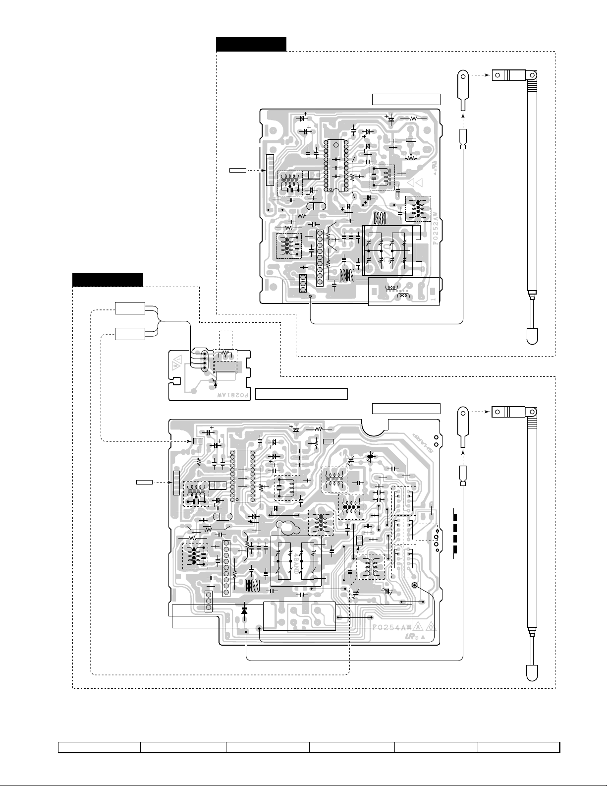
Page 24

GX-CH170X/CH170Z
GX-CH170X
A
COLOR
BR RD(R) OR YL GR BL VL GY WH(W) BK PK
TABLE
PINKBLACKWHITEGRAYVIOLETBLUEGREENYELLOWORANGEREDBROWN
B
6
CNP1
P21 9 - B
TO TUNER PWB
1
C
D
FW652
1
F651
3
3
BI651
1
D652
D651
C652
C651
D654
C654
D653
C653
T651
POWER TRANSFOMER
SO651
SO651
AC INPUT
AC220-240V
50Hz
CNS651
BR
1
RD
2
OR
3
E
13
FW652
F
(255)
T2.5A
L 250V
T. F
BATTERY DC 12V
["D" size (UM/SUM-1, R20 or HP-2)
battery x 8]
G
BATTERY
SPRING
(204)
TERMINAL PWB-A5
POWER PWB-A2
H
1
2
34 5
6
Figure 24 WIRING OF P.W.BOARD (3/8)
– 24 –
Page 25

SW651
FUNCTION
TUNER
TAPE
CD OFF
FM AUTO
BAND
SW253
GX-CH170X/CH170Z
DUBBING SPEED
AM
HIGH NORMAL
BEAT CANCEL
SW251
RD
B
A
1
FW751
P30 6 - C
TO µ-COM PWB
12
1
6
P31 11 - H
CNP602
TO DECK PWB
P31 11 - H
CNP603
TO DECK PWB
A
B
6
R500
C656
1
R651
R408
R607
ZD654
C657
ZD651
C670
R652
C655
R663
R662
R660
R676
Q654
C658
Q651
FW1
E
C
B
E
C
B
R664
R665
R655
C
D
R508
1
2
3
13
12
11
10
9
8
7
6
5
4
3
2
1
Q659
R654
R506
Q658
E
C
B
R668
CNP751
ZD653
B
C
E
R658
C659
Q653
1
2
3
D655
R507
Q655
1
2
3
R653
R673
D631
R505
R504
D656
CNP851
Q656
D632
R657
1
2
3
4
5
6
C661
R667
T500mA L 250V
R656
R502
R614
L500
F662
D633
D603
1
R503
R501
T500mA L 250V
F661
C622
C623
R659
12
FW602 FW603
R737
L450
IC500
10
9
8
C450
7
R454
Q657
Q623
C460
R452
B
C
E
Q652
6
5
4
3
2
1
C457
1
2
3
C452
3
2
1
C456
R672
Q660
B
C
R671
E
5
1
1
2
R674
Q662
3
P20 3 - H
CNS851
C459
TO CD SERVO PWB
P31 12 - C
CNS501
TO EQUALIZER PWB
6
5
4
R937
3
CNP501
2
1
11
12
13
14
C455
C458
R455
C451
C454
R451
R456
C453
15
16
17
18
19
20
R601
R615
E
C
Q522
B
R606
3
2
R675
1
CNP651
MAIN PWB-A1
R669
C669
C616
R623
C621
R621
F633
T1.25A
L 250V
IC601
C615
10111213
C609
D605
D606
C611
R609
C613
R611
J601
HEADPHONES
R616
C602
C605
C603
C506
CNP601
SPEAKERS
R605
Q521
R602
C606
C601
E
C
B
R603
R604
L-CHR-CH
D604
D601
D602
C612
R612
C604
12345678
C608
C614
9
C610
R610
78 9101112
Figure 25 WIRING OF P.W.BOARD (4/8)
– 25 –
Page 26
GX-CH170X/CH170Z
GX-CH170Z
A
COLOR
BR RD(R) OR YL GR BL VL GY WH(W) BK PK
TABLE
PINKBLACKWHITEGRAYVIOLETBLUEGREENYELLOWORANGEREDBROWN
B
5
CNP1
P21 8 - F
TO TUNER PWB
1
C
D
FW652
1
CNS651
BR
1
RD
2
OR
3
3
3
BI651
1
E
D652
C652
C651
F651
T2.5A
L 250V
D651
13
FW652
F
(255)
D654
C654
D653
C653
POWER TRANSFOMER
SO651
T651
SO651
AC INPUT
AC110-127/220-240V
50/60Hz
T. F
BATTERY DC 12V
["D" size (UM/SUM-1, R20 or HP-2)
battery x 8]
G
BATTERY
SPRING
(204)
TERMINAL PWB-A5
POWER PWB-A2
H
1
2
34 5
6
Figure 26 WIRING OF P.W.BOARD (5/8)
– 26 –
Page 27
GX-CH170X/CH170Z
FW751
P30 6 - C
TO µ-COM PWB
TAPE SELECTOR
STEREO
1
2
3
4
5
CNP851
6
Q656
R656
C661
R667
FM MODE
R502
T500mA L 250V
F662
T500mA L 250V
D633
D603
R614
SW651
FUNCTION
TUNER
TAPE
CD OFF
A
B
R500
L500
R408
R607
ZD654
R651
ZD651
C657
C670
R652
C656
C655
R663
R662
R660
5
1
R676
Q651
Q654
C658
FW1
E
C
B
E
C
B
R664
R665
R655
C
D
13
12
11
10
R508
1
2
3
9
8
7
6
5
4
3
2
1
Q659
R654
R506
Q658
E
C
B
R668
CNP751
ZD653
B
C
E
R658
C659
Q653
Q655
1
2
3
D655
R507
1
2
3
R653
R673
D631
R505
R504
D656
D632
R657
SW253
R501
R503
F661
C623
NORMALCrO2
MONO
B
A
Q661
R659
L501
R670
1
FW602 FW603
C452
R454
C460
1
2
Q657
3
3
C622
2
Q623
1
3
2
1
L450
C450
R452
B
C
E
Q652
DUBBING SPEED
HIGH NORMAL
BEAT CANCEL
SW251
R672
R671
R657
12
1
R737
1
2
R674
Q662
3
6
5
4
3
CNP501
C456
2
1
11
12
13
14
C455
15
16
17
18
R455
19
20
C458
IC500
10
9
8
7
6
5
4
3
2
1
C457
RD
Q660
C451
B
A
B
C
E
6
R451
C453
R456
C454
R937
C459
P20 3 - H
CNS851
TO CD SERVO PWB
P31 12 - C
CNS501
TO EQUALIZER PWB
1
12
1
6
P31 11 - H
CNP602
TO DECK PWB
P31 11 - H
CNP603
TO DECK PWB
R601
R615
E
C
Q522
B
R606
3
2
R675
1
CNP651
MAIN PWB-A1
R669
C669
C616
R623
C621
R621
F663
T1.25A
L 250V
IC601
C615
C609
D605
D606
C611
C613
R611
J601
HEADPHONES
10111213
R609
R616
C603
C506
CNP601
C602
C605
R605
Q521
R602
C606
C601
E
C
B
R603
R604
LR
L
L-CHR-CH
D604
D601
D602
1
C610
C612
R612
C604
2345678
C608
C614
R
SPEAKERS
9
R610
78 9101112
Figure 27 WIRING OF P.W.BOARD (6/8)
– 27 –
Page 28

GX-CH170X/CH170Z
3
VOL(DATA)
C
A
B
C
TO TUNER PWB
P34 5-H
CNP1
GND
TUNER +B
FM ST
R-CH
L-CH
4
12
3
5
L500
10µH
R508
R507
1.2K
1.2K
FW1
FM MODE
SW253-A
R500
68
FM STEREO
FM MONO
L501
10µH
FOR Z
TO TUNER PWB
P34 5-C
CNP1
GND
TUNER +B
L-CH
R-CH
AM +B
1234
5
FM +B
6
FW1
FOR X
P33 8-E
TO GRAPHIC EQALIZER
PWB
CNS501
CNP501
6
L-CH
5
R-CH
GND
7.4V
234
R-CH
+B
1
L-CH
R937
TO MI
P-GND
CH7.4V
2
1
220
+B
D
E
F
G
TO CD SERVO PWB
P33 12-A
CNP602
TO DECK PWB
FOR X
P33 12-B
CNP603
TO DECK PWB
P33 12-B
CNP603
TO DECK PWB
FW603
P22 1-H
CNS851
AUDIO GND
SERVO +7.4V
SERVO GND
FW602
(TAPE OUT)L
(TAPE OUT)R
POWER-ON12V
DUB-NOR(REC+B)
SYNC-OUT
MOTOR-CONTROLE
FW603
TAPE +B
DUB-HIGH
DUB-NOR(REC+B)
SYNC-OUT
MOTOR-CONTROLE
CrO
CNP851
R-CH
L-CH
P-GND
A-GND
(REC IN)L
(REC IN)R
AUDIO+B
SYNC IN
VCC
M-GND
BC-A
BC-B
TAPE +B
DUB-HIGH
1
2
3
4
5
2
6
1
2
3
4
5
6
1
2
3
4
5
6
7
8
9
10
11
12
1
2
3
4
5
6
MAIN PWB-A1
FOR Z
R502
10K
R504
1K
R501
10K
R503
1K
R673
2
1
1
+B
3
Q656
KRC102 M
SWITCHING
+B
+B
+B
L500
10µH
R500
68
R507
R508
1.2K
1.2K
R506
CD
L-CH
TUNER
TAPE
OFF
SW651-C
FUNCTION
FUNCTION
SW651-D
CD
[0V]
R737
22K
FM AUTO
TAPE
R-CH
AM
R505
4.7K
4.7K
BAND
SW253
FM
AM
23
Q662
KRC102 M
SWITCHING
1
H
NOTES ON SCHEMATIC DIAGRAM can be found on page 16.
1
2
34 5
Figure 30 SCHEMATIC DIAGRAM (3/7)
6
– 28 –
Page 29
TO MICROCOMPUTER PWB
-E
EQALIZER
B
01
P-GND
2
1
1
L-CH
R-CH
+B
R937
220
+B
R673
1
+B
+B
2
3
1
Q656
KRC102 M
SWITCHING
+B
CH7.4V
+B
P32 4-H
FW751
VOL(DATA)
VOL(STB)
VOL(CK)
GND
432
D656
1SS133
µ-COM5V
765
MUTE
POW-ON
98
AC-ON
CD/SYC-IN
TWEET CANCEL
1210
11
13
(0V)
C661
22K
D655
+B
R671
56K
SY OUT
L450
3
1
2
330/10
1SS133
NOR
CNP751
10µH
CD-ON:
7.4V
(0V)
CD-ON:0V
(8V)
Q655
KRC102 M
SWITCHING
CrO
C454
(DT)
(STB)
10
89
(CK)
CD
TUNER
TAPE
OFF
FUNCTION
SW651-B
F662
T500mA
L 250V
F661
T500mA
L 250V
SW253-B
TAPE SELECTOR
2
Q660
2SB561 C
DUBBING
SWITCHING
C452
2.2/50
C455
2.2/50
R451
0.1
220K
16
15
IC500
TC9211P
567
R452
C450
0.1
A
B
R659
10K
+B
+B
SWITCHING
Q657
KRA102 M
Z ONLY
R672
1K
8.2K
R455
C453
C451
1/50
0.0018
19 20141311 12
17
18
VOLUMEELECTRONIC
4
123
C460
0.0018
C456
1/50
220K
8.2K
R454
SW251-B
TWEET CANCEL
C
VOLTAGE
REGULATOR
Q651
2SD468 C
11.9V
7.4V
8V
0.022
C656
R652
560
C657
100/10
VOLTAGE
REGULATOR
Q652
2SD2394 F
7.4V
8.1V
8.1V
2
1
8.1V
3
0V
D633
1SS133
R667
10K
R674
1K
Z ONLY
DUBBING SPEED/BEAT CANCEL
NOR A
SW251-A
NOR B
HIGH C
3
1
Q661
KRC102 M
2
X ONLY
11.4V
+B+12V
C655
+B
C457
0.01
+B
R456
100
0.022
C458
R607
10K
R653
7.7V ~ 8.1V
VOLTAGE
REGULATOR
2SD468 C
C658
4.7/25
R668
100K
KTC3199 GR
SWITCHING
0.01
C670
47/10
270
Q654
Q658
ZD651
R665
10K
+B
HZ9A1
+B
0.022
C459
KTC3199 GR
R623
R651
5.6(1/4W)
Fusible
R657
D631
1SS133
R664
390
ZD653
ZD654
MTZJ5.6C
NOR A
NOR B
HIGH C
R615
R616
Q522
MUTING
10K
180
D632
MTZJ5.6C
3
R675
100K
+12V
R601
1K
22K
Q521
22K
R602
1K
C621
47/10
R621
100K
POWER-ON
Q653
2SB561 C
2.2K
R656
R654
1SS133
C659
2
1
R669
820
R408
2.7(1/4W)
Fusible
FOR X
SW251-A
BEAT CANCEL
(DUBBING)
MUTING
KTC3199 GR
3.3/25
D605
1SS133
D606
1SS133
Q623
KRA102 M
MUTE
DRIVER
R676
3.3(1/4W)
Fusible
56K
1K
R655
R660
560
R662
560
R663
22K
0.01
+B
Q659
KRC102 M
SWITCHING
C669
4.7/25
+B
FOR Z
R670
1K
C601
1/50
R603
4.7K
R605
100K
C506
R604
4.7K
R606
1K
C602
1/50
C622
2.2/50
+B
22 2
1
0V
2
0.1V
3
0V
1
C608
C603
0.001
C604
2
1
3
C623
100/25
+B
CNP6511CNS651
220/25
0.001
333
1
IC601
C605
100/10
LA4597
4
POWER
0.1V
AMP.
11.2V
7
C606
100/10
0V
6
5
11.3V
D601
1SS133
D602
1SS133
R614
1K
D603
1SS133
D604
C615
0.022
1SS133
+B
FUNCTION
SW651-A
CD
TUNER
TAPE
OFF
D651 ~ D654 : RL204F
C651 ~ C654 : 0.1 [Z]
C651 ~ C654 : 0.047 [X]
C652
D652
D653
D654
C653
BI651
13
FW652
13
BATTERY DC12V [ " D " size ( UM/SUM-1, R20
TERMINAL PWB-A5
FM SIGNAL
AM SIGNAL
CD SIGNAL
PLAYBACK SIGNAL
RECORD SIGNAL
5.8V
12
C609
100/10
10.4V
13
11
0V
10.4V
9
C610
100/10
10
5.8V
8
VCC
12V
F663
T1.25A L 250V
C616
4700/20
+B
D651
C654
X : GX-CH170X
Z : GX-CH170Z
C613
1000/10
C611
0.1
(ML)
R609
3.3(1/4W)
Fusible
R610
3.3(1/4W)
Fusible
C612
0.1(ML)
C614
1000/10
CNP601
TRANSFORMER
F651
T2.5A
L 250V
C651
or HP-2 ) battery x 8
GX-CH170X/CH170Z
R612
120
R611
POWER
T651
120
+
–
–
+
T.F
J601
HEADPHONES
L-CH
SP603
TWEETER
SP601
WOOFER
SPEAKERS
SP602
WOOFER
SP604
TWEETER
R-CH
FOR X
SO651
AC SOCKET
X : AC220-240V
50Hz
Z : AC110-127
/220-240V
50/60Hz
FOR Z
Z ONLY
AC/DC
SELECTOR
POWER PWB-A2
78 9101112
Figure 29 SCHEMATIC DIAGRAM (4/7)
– 29 –
Page 30
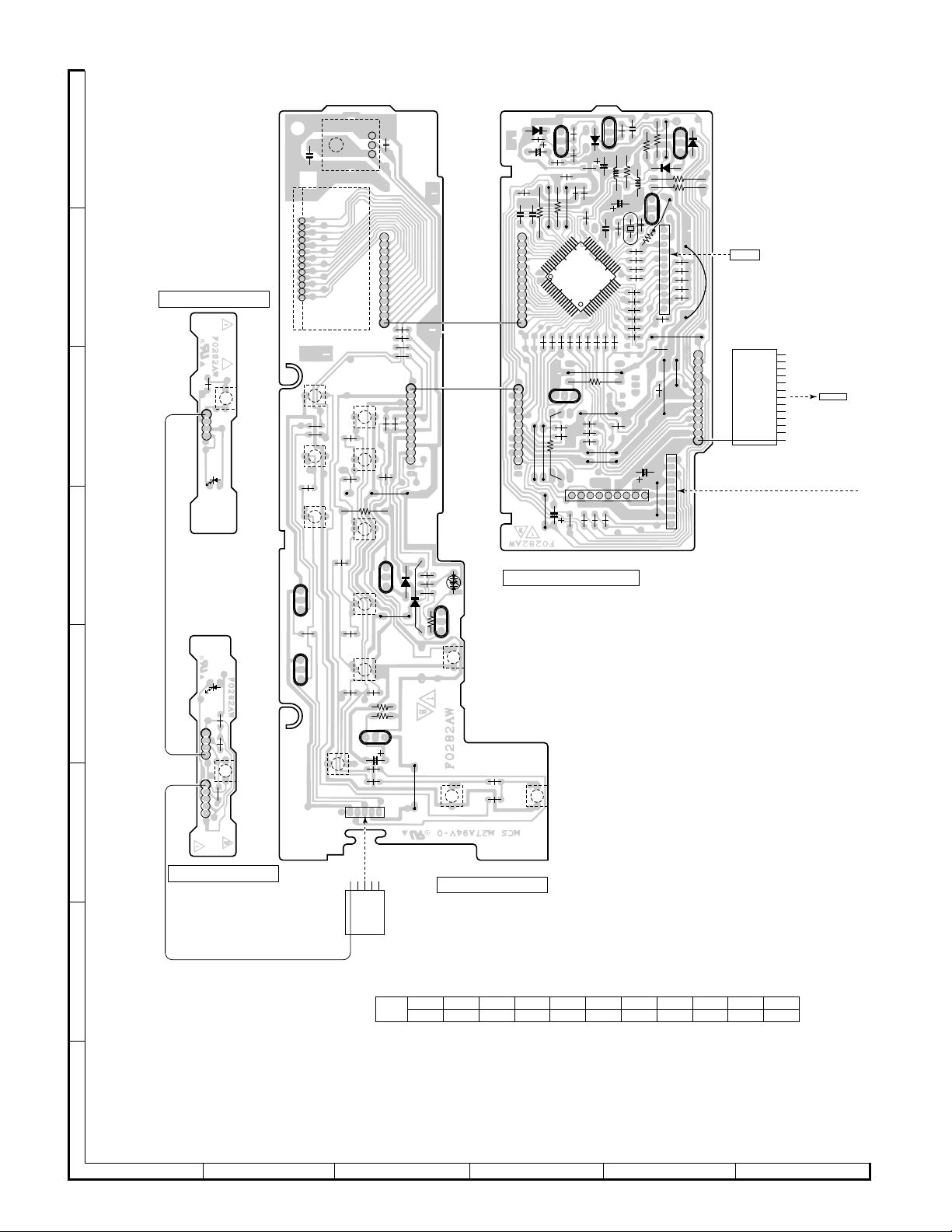
GX-CH170X/CH170Z
45
R726
C713
1
2
3
R702
Q701
1
D702
2
R747
3
R750
R755
25
10
R734
R733
R735
20
R706
4
IC761
R758
C705
C707
C706
15
R707
R727
R732
567
R759
L701
X701
R708
R720
17
16
R714
R713
R712
R711
R710
R760
R709
C703
R719
R718
R717
R716
C701
89
C712
R707
L702
3
2
1
R721
40
IC901
55
R703
R731
R730
123
R744
R754
R761
3233
35
30
5
60
1
64
R704
R705
Q705
R757
X:GX-CH170X(FO282AW)
Z:GX-CH170Z(FO281AW)
R749
Q704
R738
12
11
10
9
8
7
6
5
4
3
2
1
R736
10
9
8
7
6
5
4
3
2
1
Q703
D703
1
2
3
R748
R768
CNP852
R743
R742
R741
R740
R739
13
1
CNP753
D704
P20 4 - H
CNS852
TO CD SERVO PWB
FW751
13
P25 7 - D [X]
P27 7 - D [Z]
CNP751
TO MAIN PWB
1
Q702
3
R776
R774
STOP
SW702
SW703
DISC
SW707
PLAY
RX701
REVIEW
SW706
R775
R772
R773
R778 R771
Q715
BCE
CNP504
12345
2
1
13
1
Q713
CUE
SW705
R756
PAUSE
SW704
1
2
3
C715
R777
R779
R766
C711
R765
R789
R788
FW701
1
11
D713
R770
R762
FW702
D711
POWER
SW701
R728
R783
R784
E
C
B
UP
SW709
LED701
Q714
A
C710
1
2
3
4
5
6
7
8
9
CLEAR
SW712
10
11
12
13
RANDOM
SW708
R782
PROGRAM
SW711
LCD801
B
SWITCH PWB-A7
SW713
OPEN/CLOSE
R787
1
C
FW505
4
LED703
D
1
2
Q712
3
1
2
Q711
3
14
1
5
LED704
R785
FW505
R786
SW714
FW504
OPEN/CLOSE
E
D701
R746
C704
R745
R753
R752
C709
C708
R722
13
48
50
49
FW701
1
R701
R724
1
ECB
FW702
11
MICRO-COM PWB-A3
VOLUME
DWN
R780
SW710
R781
F
SWITCH PWB-A8
51
DISPLAY PWB-A4
G
BR RD(R) OR YL GR BL VL GY WH(W) BK PK
COLOR
TABLE
PINKBLACKWHITEGRAYVIOLETBLUEGREENYELLOWORANGEREDBROWN
H
1
2
34 5
6
Figure 30 WIRING OF P.W.BOARD (7/8)
– 30 –
Page 31
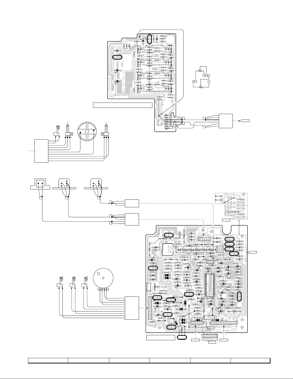
TRAY/MECHANISM UP
CNS753
10
9
8
7
6
5
4
3
2
1
SW981
BK
WH
GY
VL
BL
GR
YL
OR
RD
BR
SW983
TRAY2
C910
B
CE
Q902
C920
C921
GRAPHIC EQUALIZER PWB-A6
M981
LOADING
SW982
TRAY1
R935
R932
R936
C918
12 34
VR901
R904
12 34
VR902
1
VR903
1
R926
VR904
R910
R917
R918
R925
R903
R909
2
2
C901
C902
R931
R915
E
C
B
C919
R916
C903
C904
C911 R919
R920
C912
C915
R928
C916
R912
Q901
C917
R914
R913
R921
R922
R927
R905
R906
R911
R901
R902
C909
R930
R929
R907
R923
R924
7
BI501
1
C906
C907
C914
34
34
R933
R908
WH
PK
BK
BK
RD
PK
WH
R934
GX-CH170X/CH170Z
5
6
5
C905
6
5
C908
6
5
C913
6
CNW502
VR901 ~ VR904
A
B
543
61 2
CNS501
WH
6
PK
5
BK
4
RD
3
PK
2
WH
1
P25 11 - D [X]
P27 11 - D [Z]
CNP501
TO MAIN PWB
ERASE HEAD
WH
TAPE 1
(47)(13)
PLAY/BACK HEAD
BK
WH
TAPE1
MAIN
PK
BK
SW602SW601
TAPE2
MAIN
PLAY/BACK HEAD(47)
SW603
TAPE1/2
SELECTOR
TAPE 2
WH
PK
BK
GY
GY
BR
M601
TAPE MOTOR
–+
HL
CNS201
PK
3
BK
2
WH
1
PK
5
BK
4
WH
3
BK
2
WH
1
CNS202
C361
R255
1
3
2
Q252
R355
C353
R354
R351
C356
R352
Q351
ECB
R353
D202
L351
D203
C354
VR391
TAPE
SPEED
CNS204
BK
10
WH
9
GY
8
VL
7
BL
6
GR
5
YL
4
OR
3
RD
2
BR
1
10
9
8
CNP204
7
6
5
4
3
2
1
C393
R391
ECB
L391
D392
C391
R399
C229
R262
Q394
R385
R229
R239
ECB
R387
R392
R386
R254
R381
SW201 P. B REC
R231
R211
C245
R207
R213
C221
C239
R261
123
R384
C394
C392
R382
Q391
D264
ECB
Q392
Q393
DECK PWB-C
A
R205
C215
C225
C235
C227
C260
Q201
R383
ECB
Q253
B
C217
R215
ECB
D253
D250
D262
D261
R268
C351
R356
C204
C203
C
R203
R209
C219
R227
R225
R219
R259
D252
FW603
P25 12 - C [X]
P27 12 - C [Z]
TO MAIN PWB
C207
C244
12345
D
C205
R201
R217
C231
R223
C233
R221
C237
R237
R241
R243
R260
R236
CNP603
CNP202
E
C206
C201
CNP201
C209
24
20
15
13
C250
R250
X:JUMPER
Z:D252
123456
123
X ONLY
C362
ECB
C352
ECB
Q363
F
C211
C213
IC201
C249
1234512345 6789101112
FOR X
CNP603
FOR Z
R204
C202
1
C214
5
10
12
R264
C240
R238
D251
P25 12 - B [X]
P27 12 - B [Z]
TO MAIN PWB
R202
C208
C210
C234
C242
R218
C243
FW602
Q352
C212
C241
C238
ECB
R224
C228
R226
R230
Q362
ECB
Q353
R206
C216
R212
C220
R216
C232
R222
R232
CNP602
C367
R228
C236
E
C
B
R220
R240
R367
R368
R357
R358
C357
C218
R210
C246
R208
R214
C222
C226
C230
Z ONLY
Q202
78 9101112
Figure 31 WIRING OF P.W.BOARD (8/8)
– 31 –
Page 32
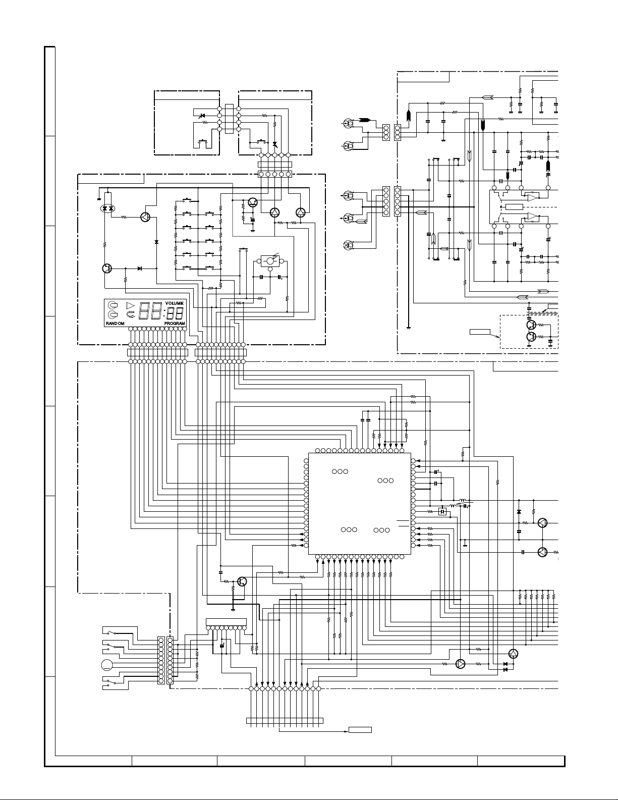
GX-CH170X/CH170Z
C
0
1
6
5
K
1
6
68K
3
6
K
5
R
A
B
C
DISPLAY PWB-A4
LED701
3N4PDN33
P-ON
GREEN
ST-BY
RED
R783
330
R784
330
Q714
KTC3199 GR
R728
47K
1
2
FW701
D
SWITCH PWB-7
LED703
3N4GDN32
R787
12K
SW713
TRAY1
OPEN/CLOSE
Q711 ~ Q715 :
+B
LED CONTROL
CLEAR
SW712
REVIEW
PROGRAM
R782
1
5.6K
23
R781
3.9K
Q713
KRA102 M
R780
2.7K
D713
1SS133
R779
1.8K
D711
R778
1.5K
1SS133
LCD801
4321
9876
5
4
8
321
9
765
21
41
3
9876
5
SW711
VOL-DOWN
SW710
VOL-UP
SW709
RANDOM
SW708
DISC 1-2
SW707
13121110
13121110
13121110
SW706
CUE
SW705
PAUSE
SW704
PLAY
SW703
STOP
SW702
R771
10K
+B
+B
1011
986
7
1011
98 6
7
+B
+B
GND
PWR-ON
AC-ON HI
E
F
C713
0.022
R726
47K
CNS705
CHANGER
MOTOR
CONTROL
SW981
G
TRAY/
MECHANISM UP
SW983
TRAY2
M981
LOADING
MOTOR
SW982
TRAY1
–
M
+
UP-SW
GND
GND
GND
MO1
MO0
2-b
2-a
1-b
1-a
CNS7531CNP753
10
1
0
9
9
8
8
7
7
6
6
5
5
4
4
3
3
2
2
1
R757
3.9K
R758
6.8K
R759
15K
89
C701
H
NOTES ON SCHEMATIC DIAGRAM can be found on page 16.
1
2
SWITCH PWB-8
33
11
KTC3199 GR
R788
5.6K
3.9K
R789
2.7K
POWER
SW701
TRY1 LED
Q705
R727
+B
FW751
FW504
CNP504
Q715
4.7K
47K
1
µ-COM5V
VREF
REMOCON
KEY1
KEY2
47K
1234
R730
TRAY2
OPEN/
CLOSE
SW714
FW702
15K
+B
1
P-GND
R786
C715
RX701
2
C711
560P
R756
10K
234
CH7.4V
12
1
330
47/6.3
R731
VOL(DATA)
44
22
FW505
R777
R776
R775
R774
1.8K
R773
1.5K
R772
10K
R762
22K
432
5
432
5
PWR-IN
TRY2 LED
KTC3199 GR
IC761
BA6218
567
100/10
34 5
Figure 32 SCHEMATIC DIAGRAM (5/7)
3
234
2
1
3
3
C710
15K
567
VOL(CK)
VOL(STB)
+B
330
R785
LED704
3N4PDN32
4
5
5
+B
Q711
KRC102 M
R766
R765
10K
1
0.1
100
R770
+B +B
R701
1K
+B
89
GND
MUTE
µ-COM5V
2
3
10K
49
50
51
52
53
54
55
56
57
58
59
60
61
62
63
64
R724
1K
R702
1K
10 11
AC-ON
POW-ON
– 32 –
Q712
1
48
SEG12
SEG11
SEG10
SEG9
SEG8
SEG7
SEG
SEG
SEG
SEG
SEG
SEG
SEG
TR1 LED
TR2 LED
MTR1
123
12 13
SYC-OUT
CD/SYC-IN
TWEET CANCEL
KRC102 M
R735
TAPE2
PLAYBACK HEAD
L-CH
R-CH
TAPE1
RECORD/PLAYBACK
HEAD
L-CH
R-CH
ERASE HEAD
C709
0.022
COM0
COM1
COM2
SEG16
48
4647
SEG13
SEG14
SEG15
IC901
IX0146AW
SYSTEM
MICROCOMPUTER
PWR-0N
MTR2
PWR-IN
12
3
DATA(VOL)
STB(VOL)
MUTE
CK(VOL)
4
89
567
220
R704
R706
R708
R707
R705
R703
R736
4.7K
22K
R732
22K
22K
R734
R733
P29 7-A
TO MAIN PWB
CNP751
VLC1
COM3
SYC-OUT
RES
10 11 12 13
R710
R709
10K
R722
C708
2.7K
VLC2
CQCK
R711
VLC3
14
C0IN
0.022
3738394041424344454647
UP-SW
MODEL
SL–
15
RWC
R712
CNS201
1
2
3
CNS202
1
2
3
4
5
1K
R721
36
CD/SYC-IN
TRAY SW
REMOCON
33
3435
KEY2
SRS1
SRS2
16
SL+
14
R714
R713
KEY1
DECK PWB-C
R201
1K
R202
CNP201
C201
1
2
3
C203
150P
CNP202
1
2
3
4
5
C204
150P
IC201 : PLAYBACK AND RECORD
R755
4.7K
R754
10K
R753
10K
R752
10K
R761
1K
33
3435
32
AC/DC
31
30
VREF
29
AVSS
28
XC-IN
27
XC-O
26
VDD
25
VSS
24
R720
X-OUT
23
X-IN
22
21
RESET
20
PU-IN
WRQ
19
SQ-OUT
18
DRF
17
16
15
R716 ~ R720 : 1K
R704 ~ R714 : 1K
1K
680P
C202
680P
SW201-D SW201-C
C205
680P
C206
680P
PPRR
SW201-ESW201-F
R232
/PLAYBACK AMP.
R760
22K
C707
100/10
C706
0.022
X701
4MHz
R719
R718
R717
R716
+B
+B
R750
3.3K
10K
1.5µH
PRPR
R203
1K
R204
1K
L701
1
KRC102 M
R220
R219
33K
56
R209
R205
150K
150P
C217
47/10
C215
0.022
C209
330P
321
C210
330P
C216
47/10
R210
150K
150P
56
R206
C361
X: 180P
Z: 0.001
C362
0.001
Q362
Q363
D702
1SS133
R751
1K
0.01
C703
C712
56P
BEAT CANCEL
R738 ~ R743, R767 : 1
R767
+B+B
2
Q703
KRA102 M
3
D704
1SS133
33K
470P
C228
R211
R207
6.8K
C219
C218
0.022
R208
3.3K
R744
2
23
Q704
KRC102 M
R738
R739
R740
6.8K
C245
560P
1/50
C220
1/50
C246
560P
6.8K
R212
6.8K
R367
5.6K
R368
5.6K
C367
0.022
RESET
Q702
KRC102 M
1
1
R741
R221
21222324
4
X ON
3
D701
1SS13
R742
6.8K
R2
5.
R21
6.8
R216
R2
5.
C
0.
R7
10
R743
R222
6.8K
R231
10K
C213
C211
150P
C207
330P
C208
330P
C212
150P
C214
KTC3199 GR
Z ONLY
KTC3199 GR
1/50
23
Q701
R747
10K
+B
L702
1.5µH
R749
1K
MICROCOMPUTE
R748
2.2K
1
D703
1SS133
+B
+B
+B
C705
+B
6
Page 33

220
R219
33K
33K
C227
470P
6.8K
470P
R221
C228
R211
C229
6.8K
C218
0.022
R207
6.8K
C219
1/50
C220
C246
560P
R208
6.8K
R212
C245
1/50
6.8K
R368
5.6K
C367
0.022
560P
R367
5.6K
R215
6.8K
4
X ONLY
R213
5.6K
R214
5.6K
R216
C230
0.001
0.001
C221
R217
2.7K
R218
2.7K
6.8K
KTC3199 GR
KTC3199 GR
C222
0.0015
0.0015
C351
X: 560P
Z: 0.001
Q352
Q353
C225
5
C226
C352
0.001
C215
C209
330P
C210
330P
C361
X: 180P
Z: 0.001
Q362
3199 GR
Q363
3199 GR
R205
C216
R206
C362
0.001
56
47/10
3
47/10
56
R209
150K
R210
150K
C217
0.022
ROCOMPUTER PWB-A3
R745
RESET
1K
Q702
R741
3
D701
1SS133
R742
R768
10K
R743
R746
100K
C704
3.3/25
3.3K
R744
1SS133
2
R751
1K
0.01
C712
56P
23
Q704
KRC102 M
BEAT CANCEL
R738 ~ R743, R767 : 15K
R738
R767
R739
R740
B
2
Q703
KRA102 M
3
D704
1SS133
3
KRC102 M
1
1
R239
0.018
L : T1
6
C241
0.018
R240
R264
100K
10K
C231
0.001
6.8K
R223
1819202122
7
10/16
6.8K
R224
C232
10K
R357
2.7K
R358
2.7K
C357
0.022
P28 6-A
CNP501
TO MAIN PWB
CD5V
12
CD-GND
11
PUIN
10
WRQ
9
SQOUT
8
DRF
7
SL–
6
SL+
5
RWC
4
COIN
3
CQCK
2
RES
1
CNP852
R243
56K
C249
100/10
47
R227
560
C237
R225
C235
0.082
C233
22/16
17
8
C234
22/16
C236
0.082
R226
560
0.001
C238
47
R228
X ONLY
C353
Z ONLY
P22 1-G
CNS852
TO CD SERVO PWB
0.0033
16
9
0.0033
0.0039
CNS501
1
2
3
4
5
6
C239
2.2/50
C240
C354
0.027
(ML)
R229
R230
2.2/50
R351
47K
10K
10K
BI501
15
C242
1
2
3
4
5
6
7
R241
12K
R237
10K
C244
IC201
AN7345K
0.082
R238
680K
R352
100K
R353
22
R250
100
FOR Z
R236
C250
10K
220/10
Q201
MUTING
47
C921
100/10
KTC3199 GR
FOR X
R259
R261
27K
C260
R260
4.7K
Q202
KTC3199 GR
R355
47
Q901
KTC3199 GR
R935
3.9K
R936
D252
4.7K
1/50
R933
1K
2.9V
2.9V
3.9K
22/16
14
C243
13
121110
33/16
C356
47/10
Q351
2SC2001 K
BIAS OSC.
L351
330µH
MUTING
R354
R934
1K
FM SIGNAL
PLAYBACK SIGNAL
RECORD SIGNAL
D251
1SS133
SW201-B SW201-A
4.7K
D203
R262
1SS133
D202
1SS133
D253
1SS133
D250
1SS133
23
R254
Q252
1
22K
KRC102 M
C919
1/50
R931
680K
0.65V
C917
0V
330P
C918
0V
330P
0.65V
R932
680K
C920
1/50
10K
R255
C392
47/10
R385
10K
C394
0.022
VR904-A
100K(B)
R929
2.2K
Q902
KTC3199 GR
R926
8.2K
VR904-B
100K(B)
R930
2.2K
R356
PRPR
47
R381
33K
R383
18K
R382
18K
R384
2.7K
R268
15K
Q391
KTC3199 GR
SWITCHING
Q393
KRC102 M
3
1
R925
8.2K
R927
8.2K
C913
0.0027
R928
8.2K
R924
1.2K
GRAPHIC EQUALIZER
D262
1SS133
D261
1SS133
1
3
2
Q253
KRA102 M
R386
R387
1.8K
56K
Q392
2SB562 C
R399
1.8K
C391
D392
1SS133
2
Q394
KTC3199 GR
SWITCHING
R917
6.8K
330P
C915
VR903-A
100K(B)
R921
5.6K
R923
1.2K
R918
6.8K
330P
C916
VR903-B
100K(B)
R922
5.6K
C914
0.0027
X : GX-CH170X
Z : GX-CH170Z
L391
47µH
100/25
R919
6.8K
C907
0.0068
C909
0.022
R920
6.8K
C908
0.0068
C910
0.022
C911
C912
C393
R391
D264
0.022
10K
R392
4.7K
0.0022
0.0022
1SS133
VR902-A
100K(B)
R913
6.8K
VR902-B
100K(B)
R914
GX-CH170X/CH170Z
CNP602
L
1
(TAPE OUT)
R
2
A-GND
3
L
4
(REC IN)
R
5
AUDIO+B
6
SYNCIN
7
POWER-ON12V
8
VCC
9
GND
11
BC-A
12
BC-B
13
TAPE
1
High (Hi)
2
Nor
3
SYNC OUT
4
MO CON
5
CrO
2
6
Z ONLY
CNP603
1010
9
9
8
8
7
7
6
6
5
5
4
4
3
3
2
2
1
1
MECHA
GND
VR391
CNP204
CNS204
GRAPHIC EQUALIZER PWB-A6
X-BASS10kHz 2kHz 500Hz
R903
33K
C903
VR901-A
0.0056
R911
18K
C905
0.0082
R912
18K
C906
0.0082
C904
0.0056
R915
18K
R916
18K
R907
39K
VR901-B
R904
33K
R908
39K
R905
R906
68K
68K
6.8K
R909
R910
15K
4.7K(B)
TAPE
SPEED
15K
P30 1-G
FW602
TO MAIN PWB
P30 1-G
FW603
TO MAIN PWB
H
L
–
+
L-CH(IN)
0.01
C901
R-CH(IN)
0.01
C902
M
SW603
T1/T2
SELECTOR
SW602
TAPE2
MAIN
SW601
TAPE1
MAIN
M601
TAPE
MOTOR
78 9101112
Figure 33 SCHEMATIC DIAGRAM (6/7)
– 33 –
Page 34
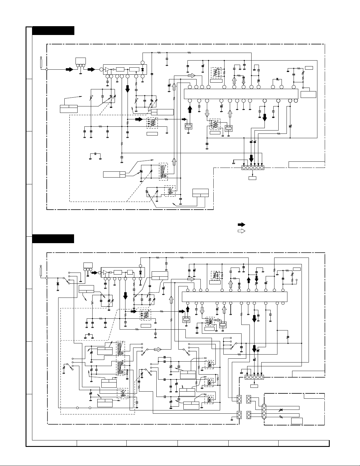
GX-CH170X/CH170Z
GX-CH170X
A
B
C
D
ROD
ANTENNA
CNW2
fLFMfH
TRACKING
B. P. F.
123
C16
0.0047
F1
L1
FM ANT
C9
0.0047
C11
220P
220P
22P
(CH)
C4
FM FRONT END
RF AMP
1
2
3
C2
0.001
TC1 VC1
R1
10
C15
0.022
AM
TRACKING
IC1
LA1186N
MIX
VCC
96
5
+B
R7
390
C17
0.022
fL
fH
OSC
22K
R2
33
L2
FM
R9
C10
0.022
OSC
8
C5
33P
(CH)
C6
15P
(RH)
TC4 VC4
7
4
TC3
TC2
T1
FM IF
C8
4P
(CH)
fH
VC3
R5
330K
C29
10/16
VC2
FM BAND
COVERAGEfL
R3
47
L3
AM BAR ANT.
AM OSC.
C14
0.022
C39
C37
0.022
220/10
24 23 22 21 20 19 18 17 16 15 14 13
AM
STB AM RF +B FM DET AM
OSC
R25
120
FM IF IN
1
C20
0.022
31
CF2
2
AM BAND
COVERGE
fL fH
C36
L4
0.022
2
AM MIX
T2
R26
3.9K
FM DET
AM IFAGC
4
3
+B
C21
0.022
22/16
T3
AM IF
C26
57
1
2
C22
0.0022
R27
33K
AM
IN
OUT
ST
IND
GND
68
3
CF3
+B
CNP1
1
TO MAIN PWB
C38
0.022
C23
0.0082
DET
OUT
TUN
IND
C33
1/50
234
FW1
P28 4-C
MPX-IN
C31
C31
C34
5
0.022
0.022
C24
470P
C25
3.3/50
1/50
+B
6
3.3/50
C28
0.0015
R-CHL-CH
R35
1.8K
VCO
AM/FM
121110
FM/AM IF MPX.
C35
1/50
FM-M/ST
9
9
C32
0.022
TUNER PWB-B
R30
1.2K
MPX VCO
CK 76kHz
IC2
LA1805
+B
VCO
VR1
6.8KC27
R29
15K
+B
R6
820K
GX-CH170Z
ROD
ANTENNA
E
F
G
H
CNW2
SW1-A
BAND
D1
1SS133
BAND
SW1-B
VC3
MW
SW1
SW2
FM
MW
SW1
SW2
FM
1
FM
TRACKING
fL fH
C16
0.0047
TC3
CNW3
F1
C11
220P
2
3
L1
FM RF
TC5
FM FRONT END
RF AMP
1
2
C2
0.001
C4
18P
(CH)
R1
10(AX)
C9
0.0047
C15
0.022
fL fH
MW
TRACKING
C41
(CH)
2P
fH fL
SW1
TRACKING
TC7
fH fL
SW2
TRACKING
IC1
LA1186N
3
5
VC1
TC1
BAR ANT.
L3
MIX
VCC
MW
SW1
L6
SW2 ANT.
FM SIGNAL
AM SIGNAL
R5
330K
7
OSC
689
R2
33
C5
33P
(CH)
L2
FM
OSC
R9
22K
C10
0.022
R11
120
15P
R7
SW1
SW2
2.2K
C6
MW
FM
4
SW1-F
BAND
C51
0.022
C55
2.7P
100
R50
T1
FM IF
VC4
TC2
BAND
SW1-C
FM BAND
COVERAGE
fL fH
C8
3P
(CH)
VC2
R3
47
C17
0.022
180P(CH)
MW
SW1
SW2
FM
0.0015
10P(UJ)
C56
C46
180P
(CH)
C44
C42
0.0047
C49
R6
820K
C14
0.022
C39
0.022
220/10
C29
R25
120
24 23 22 21 20 19 18 17 16 15 14
10/16
AM
STB +B
OSC
FM IF IN
12
C20
0.022
123
CF2
C21
0.022
MW
SW1
SW2
SW1-E
FM
BAND
C48
5P
(CH)
fH fL
MW BAND
COVERAGE
TC4
fH fL
SW1 BAND
COVERAGE
C50
5P(UJ)
fH fL
SW2 BAND
COVERAGE
39
R42
R40
39
TC6
TC8
T2
C37
FM DET
AM RF FM DET MPX-IN
AM MIX
AGC AM IF
4
3
MW OSC.
SW1 OSC.
SW2 OSC.
AM IF
L5
L4
L7
22/16
T3
C26
567
1
2
R43
1.8K
R26
3
MW
SW1
SW2
FM
C22
0.0047
3.9K
OUT IN
GND
CF3
BAND
SW1-D
CNP3
CNP2
R36
680
C40
0.022
10(AX)
C38
0.022
C24
R27
33K
R35
470P
C25
C23
AMAM
ST
IND
+B
1
2
1
2
0.0082
DET
OUT
TUN
IND
89
1
1
2
CNS3
CNS2
1
2
L-CH
L-CH
C33
234
FW1
C34
1/50
1/50
5
P28 3-B
TO MAIN PWB
3.3/50
R-CH
C31
0.015
R-CH
CNP1
1
2
3
4
FM-M/ST
BI500
R30
1.2K
C28
0.0015
13
VCO
121110
FM/AM IF
0.015
VCO
VR1
6.8K
R29
15K
MPX VCO CK
76kHz
IC2
LA1805
C35
1/50
+B
+B
R28
100K
C27
3.3/50
AM/FM
C32
TUNER PWB-B
PWB-A9
LED500
3N4PDN32
VR500
5K(B)
FINE
TUNING
NOTES ON SCHEMATIC DIAGRAM can be found on page 16.
1
2
34 5
Figure 34 SCHEMATIC DIAGRAM (7/7)
– 34 –
6
Page 35

WAVEFORMS OF CD CIRCUIT
GX-CH170X/CH170Z
1
1
2
3
4
5
3
5ms
0.50 V
IC801 20 F.E
5ms
5.0 V
IC801 54 DRF
0.5ms
1.00 V
HF
0.5ms
5.0 V
HFL
0.5ms
5.0 V
TES
0.5ms
1.00 V
H.F
STOP PLAY
FOCUS SERCH
3
1
CUE
1
2
3
REVIEW
6
7
8
9
6
7
8
9
10
11
50ms
10.0 V
JP+
50ms
10.0 V
JP-
50ms
0.50 V
JP
50ms
1.00 V
TE
0.5ms
10.0 V
JP+
0.5ms
10.0 V
JP-
0.5ms
0.50 V
JP
0.5ms
1.00 V
TE
20ms
1.00 V
SPO
20ms
2.00 V
CLV+
REVIEW
PLAY
NORMAL DISC
TN0=01
0.5ms
4
5
6
7
8
9
6
7
8
9
5.0 V
HFL
0.5ms
5.0 V
TES
50ms
10.0 V
JP+
50ms
10.0 V
JP-
50ms
0.50 V
JP
50ms
1.00 V
TE
0.5ms
10.0 V
JP+
0.5ms
10.0 V
JP-
0.5ms
0.50 V
JP
0.5ms
1.00 V
TE
1
2
3
CUE
10
11
12
12
50ms
1.00 V
SPO
50ms
2.00 V
CLV+
5s
100mV
SLD
0.5s
100mV
SLD
PLAY
TCD-712 (140mm)
TN0=01
PLAY
TCD-712
1
1
– 35 –
Page 36

GX-CH170X/CH170Z
FUNCTION TABLE OF IC
IC901 RH-iX0146AWZZ (IX0146AW): System Control Microcomputer
Pin No. Function
1 P03 MTCONT2 Output Changer mechanism motor control output No.2.
2 P10 POWER IN Input Power key input.
3 D0 POWER ON Output "L" when power is turned on.
4 P12 DATA(VOL) Output Electronic volume data.
5 P13 STB(VOL) Output Volume change after data fetching.
6 P11 CK(VOL) Output Electronic volume data fetch timing signal.
7 D1 MUTE Output System mute signal output.
8 D2 SYNC OUT Output Deck motor control output. "H" when REC is required for CD function.
9 D3 RES Output Reset output.
10 D4 CQCK Output Serial data sync clock for interface.
11 D5 COIN Output Servo control signal processing IC command output.
12 D6/CNTR0 RWC Output READ/WRITE control output. (from microcomputer)
13 D7/CNTR1 SL+ Output Slide motor feed output.
14 D8/INT0/ZEROX SL- Output Slide motor return output. SL+/SL- combination control. Track count monitor
15* D9/SCK/RTP0 SRS2 Output Surround control output 2.
16* D10/SOUT/ SRS1 Output Surround control output 1. Surround control with SRS1 and 2.
17 P20/SIN DRF Intput HF level detection input.
18 P21/INT1 SQOUT Input Sub-code Q data input.
19 P22 WRQ Input Detection input for sub-Q code output standby.
20 P23 PU IN Input CD pickup position detection. Innermost periphery: "L"
21 RESET RESET Input If "L" state is held for more than 0.75 usec (one machine cycle), reset state isset
22 X IN X IN Input Main clock input.
23 X OUT X OUT Output Main clock output.
24 VSS D GND — Power terminal GND (0V)
25 VDD D +5V — Power terminal +5V
26 XCOUT SU CLOUT Output Sub-clock output.
27 XCIN SU CLIN Input Sub-clock input
28 AVSS ADGND — A/D converter reference voltage GND terminal (0V is applied)
29 VREF AD +5V — A/D converter reference voltage input terminal.
30 SEG26/P30/ REMOCON Input Remote control signal input.
31 SEG25/P31/AIN1 AC/DC Input AC/DC discrimination port. AC: "L" DC: "H"
32 SEG24/P32/AIN2 CD FUNC/ Input Function/REC detection.
33 SEG23/P33/AIN3 KEY1 Input Operation key input No.1.
34 SEG22/P40/AIN4 KEY2 Input Operation key input No.2.
35 SEG21/P41/AIN5 MODEL Input Model discrimination when power is turned on.
36 SEG20/P42/AIN6 TRAY SW Input Changer mechanism switch input. 5-position analog input.
37 SEG19/P43/AIN7 UP/LID SW Input Open TOP type: LID SW port. Changer type: Mechanism UP SW port.
38 VLC3 VLC3 Input LCD bias setting power terminal.
39 SEG18/VLC2 VLC2 Input Internal divided resistor is connected. 1/3 bias, 1/4 duty
40 SEG17/VLC1 VLC1 Input Internal divided resistor is connected.
41-44 COM3-COM0 COM3-COM0 Output LCD control common terminal (1/4 duty).
45-61 SEG16-SEG0 SEG16-SEG0 Output LCD control segment terminal.
(45*-52*)
62 P00 TR1 LED Output For CD changer validity indication. For output tray No.1.
63 P01 TR2 LED Output For CD changer validity indication. For output tray No.2.
64 P02 MTCONT1 Output Changer mechanism motor control output No.1.
Terminal
Name
RTP1/PWM However, since Surround has three positions, "H, H" is not used.
INT2/AIN0 To be detected at fall edge.
In this unit, the terminal with asterisk mark (*) is (open) terminal which is not connected to the outside.
Port Name Input/
Output
For audio signal muting
Disc deceleration signal monitor. Track count monitor.
(in case of 4 MHz oscillation).
Applied voltage must be not lower than 2V but not higher than VDD.
SYNC-IN
– 36 –
Page 37

LCD801 RV-LX0020AWZZ
SEGMENT
S0
1
2
S1
S2
S3
S4
S5
S6
S7
GX-CH170X/CH170Z
S8
VOLUME
COMMON
RANDOM
1
2
PROGRAM
C0
C1
C2
C3
VOLUME
RANDOM
PROGRAM
Figure 37 LCD SEGMENT
– 37 –
Page 38

GX-CH170X/CH170Z
— M E M O —
– 38 –
Page 39
PARTS GUIDE
GX-CH170X/CH170Z
“HOW TO ORDER REPLACEMENT PARTS”
To have your order filled promptly and correctly, please furnish the
following information.
1. MODEL NUMBER 2. REF. No.
3. PART NO. 4. DESCRIPTION
MARK: SPARE PARTS-DELIVERY SECTION
Explanation of capacitors/resistors parts codes
Capacitors
VCC ....................... Ceramic type
VCK........................ Ceramic type
VCT ........................ Semiconductor type
VC • • MF ............... Cylindrical type (without lead wire)
VC • • MN ............... Cylindrical type (without lead wire)
VC • • TV................ Square type (without lead wire)
VC • • TQ ............... Square type (without lead wire)
VC • • CY ............... Square type (without lead wire)
VC • • CZ................ Square type (without lead wire)
VC • • • • • • • • • J .. The 13th character represents capacity difference.
("J" ±5%, "K" ±10%, "M" ±20%, "N" ±30%,
"C" ±0.25 pF, "D" ±0.5 pF, "Z" +80-20%.)
If there are no indications for the electrolytic capacitors, error is ±20%.
MODEL
GX-CH170X
GX-CH170Z
For U.S.A. only
Contact your nearest SHARP Parts Distributor to order.
For location of SHARP Parts Distributor,
Please call Toll-Free;
1-800-BE-SHARP
Resistors
VRD ....................... Carbon-film type
VRS........................ Carbon-film type
VRN ....................... Metal-film type
VR • • MF ............... Cylindrical type (without lead wire)
VR • • MN............... Cylindrical type (without lead wire)
VR • • TV................ Square type (without lead wire)
VR • • TQ ............... Square type (without lead wire)
VR • • CY ............... Square type (without lead wire)
VR • • CZ................ Square type (without lead wire)
VR • • • • • • • • • J .. The 13th character represents error.
("J" ±5%, "F" ±1%, "D" ±0.5%.)
If there are no indications for other parts, the resistors are ±5%
carbon-film type.
NOTE:
Parts marked with “ ” are important for maintaining the safety of the set.
Be sure to replace parts with specified ones for maintaining the safety and performance of the set.
Page 40

GX-CH170X/CH170Z
PRICE
RANK
DESCRIPTIONNO. PART CODE NO. PARTS CODE
INTEGRATED CIRCUITS
IC1 VHILA1186N/-1 J AE FM Front End,LA1186N
IC2 VHILA1805//-1 J AM FM/AM IF MPX.,LA1805
IC201 VHIAN7345K/-1 J AM Playback and Record/ Playback
IC500 VHITC9211P/-1 J AS Electronic Volume,TC9211P
IC601 VHILA4597//-1 J AH Power Amp.,LA4597
IC761 VHIBA6218//-1 J AH Changer Motor Control,BA6218
IC801 VHILA9240M/-1 J AV Servo Amp.,LA9240M
IC802 VHILC78622E-1 J BA Servo/Signal Control,LC78622E
IC804 VHIBA5920FP-1 J AR Focus/Tracking/Spin/Slide
IC901 RH-IX0146AWZZ J AV System,Microcomputer,
Amp.,AN7345K
Driver,BA5920FP
IX0146AW
TRANSISTORS
Q201,202 VSKTC3199GR-1 J AB Digital,NPN,KTC3199 GR
Q252 VSKRC102M//-1 J AC Digital,NPN,KRC102 M
Q253 VSKRA102M//-1 J AC Digital,PNP,KRA102 M
Q351 VS2SC2001-K-1 J AD Silicon,NPN,2SC2001 K
Q352,353 VSKTC3199GR-1 J AB Digital,NPN,KTC3199 GR
Q362,363 VSKTC3199GR-1 J AB Digital,NPN,KTC3199 GR
Q391 VSKTC3199GR-1 J AB Digital,NPN,KTC3199 GR
Q392 VS2SB562C//-1 J AC Silicon,PNP,2SB562 C
Q393 VSKRC102M//-1 J AC Digital,NPN,KRC102 M
Q394 VSKTC3199GR-1 J AB Digital,NPN,KTC3199 GR
Q521,522 VSKTC3199GR-1 J AB Digital,NPN,KTC3199 GR
Q623 VSKRA102M//-1 J AC Digital,PNP,KRA102 M
Q651 VS2SD468-C/-1 J AD Silicon,NPN,2SD468 C
Q652 VS2SD2394F/-1 J AE Silicon,NPN,2SD2394 F
Q653 VS2SB561-C/-1 J AC Silicon,PNP,2SB561 C
Q654 VS2SD468-C/-1 J AD Silicon,NPN,2SD468 C
Q655,656 VSKRC102M//-1 J AC Digital,NPN,KRC102 M
Q657 VSKRA102M//-1 J AC Digital,PNP,KRA102 M
Q658 VSKTC3199GR-1 J AB Digital,NPN,KTC3199 GR
Q659 VSKRC102M//-1 J AC Digital,NPN,KRC102 M
Q660 VS2SB561-C/-1 J AC Silicon,PNP,2SB561 C
Q661 VSKRC102M//-1 J AC Digital,NPN,KRC102 M [Z Only]
Q662 VSKRC102M//-1 J AC Digital,NPN,KRC102 M
Q701,702 VSKRC102M//-1 J AC Digital,NPN,KRC102 M
Q703 VSKRA102M//-1 J AC Digital,PNP,KRA102 M
Q704 VSKRC102M//-1 J AC Digital,NPN,KRC102 M
Q705 VSKTC3199GR-1 J AB Digital,NPN,KTC3199 GR
Q711,712 VSKRC102M//-1 J AC Digital,NPN,KRC102 M
Q713 VSKRA102M//-1 J AC Digital,PNP,KRA102 M
Q714 VSKTC3199GR-1 J AB Digital,NPN,KTC3199 GR
Q715 VSKTC3199GR-1 J AB Digital,NPN,KTC3199 GR
Q804 VS2SD468-C/-1 J AD Silicon,NPN,2SD468 C
Q805 VSKTA1266GR-1 J AB Silicon,PNP,KTA1266 GR
Q901,902 VSKTC3199GR-1 J AB Digital,NPN,KTC3199 GR
[Z Only]
[Z Only]
DIODES
D1 VHD1SS133//-1 J AA Silicon,1SS133 [Z Only]
D202,203 VHD1SS133//-1 J AA Silicon,1SS133
D250,251 VHD1SS133//-1 J AA Silicon,1SS133
D252 VHD1SS133//-1 J AA Silicon,1SS133 [Z Only]
D253 VHD1SS133//-1 J AA Silicon,1SS133
D261,262 VHD1SS133//-1 J AA Silicon,1SS133
D264 VHD1SS133//-1 J AA Silicon,1SS133
D392 VHD1SS133//-1 J AA Silicon,1SS133
D601~606 VHD1SS133//-1 J AA Silicon,1SS133
D631~633 VHD1SS133//-1 J AA Silicon,1SS133
!
D651~654 VHDRL204F//-1 J AC Silicon,RL204F
D655,656 VHD1SS133//-1 J AA Silicon,1SS133
D701~704 VHD1SS133//-1 J AA Silicon,1SS133
D711 VHD1SS133//-1 J AA Silicon,1SS133
D713 VHD1SS133//-1 J AA Silicon,1SS133
D802 VHD1SS133//-1 J AA Silicon,1SS133
D803 VHDRL104A//-1 J AB Silicon,RL104A [Z Only]
LED500 92LLED3N4PDN32 J AC LED,Red,3N4PDN32 [Z Only]
LED701 VHP3N8PGN33-1 J AE LED,Red/Green,3N8PGN33
LED703 92LLED3N4GDN32 J AD LED,Green,3N4GDN32
LED704 92LLED3N4PDN32 J AC LED,Red,3N4PDN32
ZD651 VHEHZ9A1///-1 J AB Zener,9V,HZ9A1
ZD653,654 VHEMTZJ5R6C-1 J AB Zener,5.6V,MTZJ5.6C
ZD801 VHEMTZJ5R6B-1 J AD Zener,5.6V,MTZJ5.6B
PRICE
RANK
DESCRIPTION
FILTERS
CF2 92LFILT-F1342A J A D FM IF
CF3 RFILA0006AWZZ J AG AM IF [X]
CF3 RFILA0007AWZZ J AG AM IF [Z]
F1 92LFILTF1759AT J AD FM Band Pass Filter
TRANSFORMERS
T1 RCILI0007AWZZ J AD FM IF
T1 RCILI0012AWZZ J FM IF [SERIAL No.608ЧЧЧЧЧ~]
T2 RCILI0008AWZZ J AF FM Detection
T2 RCILI0013AWZZ J FM Detection
T3 RCILI0010AWZZ J AF AM IF [Z]
T3 RCILI0014AWZZ J AE AM IF [X]
!
T651 RTRNP0091AWZZ J AZ Power
[SERIAL No.60500001~
607ЧЧЧЧЧ]
[SERIAL No.60500001~
607ЧЧЧЧЧ]
[SERIAL No.608ЧЧЧЧЧ~]
COILS
L1 RCILR0364AFZZ J AA FM RF
L2 RCILB0020AWZZ J AA FM Oscillation [X]
L2 RCILB0628AFZZ J AC FM Oscillation [Z]
L3 RCILA0048AWZZ J MW/SW1 Bar Antenna [Z]
L3 RCILA0053AWZZ J AK AM Bar Antenna [X]
L4 RCILB0047AWZZ J SW1 Oscillation [Z]
L4 RCILB0051AWZZ J AE AM Oscillation [X]
L5 RCILB0053AWZZ J AC MW Oscillation [Z Only]
L6 RCILA0556AFZZ J AD SW2 Antenna [Z Only]
L7 RCILB0048AWZZ J SW2 Oscillation [Z Only]
L351 VP-MK331K0000 J AB 330 µH,Choke
L391 VP-YF470K0000 J AB 47 µH,Choke
L450 VP-DH100K0000 J AB 10 µH,Choke
L500 VP-DH100K0000 J AB 10 µH,Choke
L501 VP-DH100K0000 J AB 10 µH,Choke [Z Only]
L701,702 VP-XH1R5K0000 J AB 1.5 µH,Choke
L801 VP-XHR82K0000 J AC 0.82 µH,Choke
VARIABLE RESISTORS
VR1 92LVRS682NBUT J AC 6.8 kohms (B),Semi-VR [VCO]
VR391 92LVRS472NBUT J AD 4.7 kohms (B),Semi-VR
VR500 RVR-B0011AWZZ J 5 kohms (B),Semi-VR
VR901 92LVRS1788B J AE 100 kohm (B),Semi-VR[X-BASS]
VR902~904 92LVRS1788A J AE 100 kohm (B),Semi-VR
[Tape Speed]
[Fine Tuning] [Z Only]
[Graphic Equalizer]
VARIABLE CAPACITORS
TC5~8 92LTO-1527AT J AF Trimmer,20 pF [Z Only]
VC1-4 92LVC-1455A J AN Variable Capacitor with
VC1-4 92LVC-197A J AS Variable Capacitor with
Trimmers (TC1~4) [X]
Trimmers (TC1~4) [Z]
VIBRATORS
X701 RCRM-0009AWZZ J AF Ceramic,4.000 MHz
XL801 RCRM-0008AWZZ J AF Ceramic,16.93 MHz
CAPACITORS
C2 VCKYMN1HB102K J AA 0.001 µF,50V
C4 VCCCPA1HH180J J AA 18 pF (CH),50V [Z]
C4 VCCCPA1HH220J J AA 22 pF (CH),50V [X]
C5 VCCCPA1HH330J J AA 33 pF (CH),50V
C6 VCCRPA1HH150J J AA 15 pF (RH),50V
C8 VCCCPA1HH3R0C J AA 3 pF (CH),50V [Z]
C8 VCCCPA1HH4R0C J AA 4 pF (CH),50V [X]
C9 VCTYPA1EX472M J AA 0.0047 µF,25V
C10 VCTYPA1EX223M J AA 0.022 µF,25V
C11 VCKYPA1HB221K J AA 220 pF,50V
C14 VCTYMN1EF223Z J AA 0.022 µF,25V
C15 VCTYPA1EX223M J AA 0.022 µF,25V
C16 VCTYPA1EX472M J AA 0.0047 µF,25V
C17 VCTYMN1EF223Z J AA 0.022 µF,25V
– 1 –
Page 41

GX-CH170X/CH170Z
PRICE
RANK
C20,21 VCTYMN1EF223Z J AA 0.022 µF,25V
C22 VCTYMN1CX222K J AA 0.0022 µF,16V [X]
C22 VCTYMN1CX472K J AA 0.0047 µF,16V [Z]
C23 VCTYPA1EX822M J AA 0.0082 µF,25V
C24 VCKYMN1HB471K J AA 470 pF,50V
C25 RC-GZA335AF1H J AB 3.3 µF,50V,Electrolytic
C26 RC-GZA226AF1C J AB 22 µF,16V,Electrolytic
C27 RC-GZA335AF1H J AB 3.3 µF,50V,Electrolytic
C28 92LCPU100V1500 J AC 0.0015 µF,100V
C29 RC-GZA106AF1C J AB 10 µF,16V,Electrolytic
C31,32 VCTYPA1EX153M J AA 0.015 µF,25V [Z]
C31,32 VCTYPA1EX223M J AA 0.022 µF,25V [X]
C33~35 RC-GZA105AF1H J AB 1 µF,50V,Electrolytic
C36 VCTYPA1EX223M J AA 0.022 µF,25V [X Only]
C37 RC-GZA227AF1A J AB 220 µF,10V,Electrolytic
C38,39 VCTYMN1EF223Z J AA 0.022 µF,25V
C40 VCTYMN1EF223Z J AA 0.022 µF,25V [Z Only]
C41 VCCCPA1HH2R0C J AA 2 pF (CH),50V [Z Only]
C42 VCCUPA1HJ100J J AB 10 pF (UJ),50V [Z Only]
C44 VCKYPA1HB152K J AA 0.0015 µF,50V [Z Only]
C46 VCCCPA1HH181J J AA 180 pF (CH),50V [Z Only]
C48 VCCUPA1HJ5R0C J AA 5 pF (UJ),50V [Z Only]
C49 VCTYMN1CX472K J AA 0.0047 µF,16V [Z Only]
C50 VCCUPA1HJ5R0C J AA 5 pF (UJ),50V [Z Only]
C51 VCTYPA1EX223M J AA 0.022 µF,25V [Z Only]
C55 VCCCMN1HH2R7C J AA 2.7 pF (CH),50V [Z Only]
C56 VCCCPA1HH181J J AA 180 pF (CH),50V [Z Only]
C201,202 VCKYMN1HB681K J AA 680 pF,50V
C203,204 VCKYMN1HB151K J AA 150 pF,50V
C205,206 VCKYMN1HB681K J AA 680 pF,50V
C207ç210 VCKYPA1HB331K J AA 330 pF,50V
C211,212 VCKYPA1HB151K J A A 150 pF,50V
C213,214 VCKYMN1HB151K J AA 150 pF,50V
C215,216 RC-GZA476AF1A J AB 47 µF,10V,Electrolytic
C217,218 VCTYPA1EX223K J AA 0.022 µF,25V
C219,220 RC-GZA105AF1H J AB 1 µF,50V,Electrolytic
C221,222 VCTYMN1CX152K J AA 0.0015 µF,16V
C225,226 VCTYPA1EX183K J AA 0.018 µF,25V
C227,228 VCKYPA1HB471K J A A 470 pF,50V
C229,230 VCKYPA1HB102K J A A 0.001 µF,50V
C231,232 VCKYMN1HB102K J AA 0.001 µF,50V
C233,234 RC-GZA226AF1C J AB 22 µF,16V,Electrolytic
C235,236 VCTYPA1CX823K J AB 0.082 µF,16V
C237,238 VCTYMN1CX332K J AA 0.0033 µF,16V
C239,240 RC-GZA225AF1H J AB 2.2 µF,50V,Electrolytic
C241 RC-GZA106AF1C J AB 10 µF,16V,Electrolytic
C242 VCTYPA1EX823K J AB 0.082 µF,25V
C243 RC-GZA336AF1C J AB 33 µF,16V,Electrolytic
C244 RC-GZA226AF1C J AB 22 µF,16V,Electrolytic
C245,246 VCKYPA1HB561K J A A 560 pF,50V
C249 RC-GZA107AF1A J AB 100 µF,10V,Electrolytic
C250 RC-GZA227AF1A J AB 220 µF,10V,Electrolytic
C260 RC-GZA107AF1H J AC 100 µF,50V,Electrolytic
C351 VCKYMN1HB102K J AA 0.001 µF,50V [Z]
C351 VCKYMN1HB561K J AA 560 pF,50V [X]
C352 VCKYPA1HB102K J AA 0.001 µF,50V [Z Only]
C353 VCQPKA2AA392J J AB 0.0039 µF,100V,Polypropylene
C354 RC-QZA273AFYJ J AB 0.027 µF,50V,Mylar
C356 RC-GZA476AF1A J AB 47 µF,10V,Electrolytic
C357 VCTYMN1EF223Z J AA 0.022 µF,25V [Z Only]
C361 VCKYMN1HB181K J AA 180 pF,50V
C362 VCKYMN1HB102K J AA 0.001 µF,50V [Z Only]
C367 VCTYMN1EF223Z J AA 0.022 µF,25V [Z Only]
C391 RC-GZA107AF1E J AB 100 µF,25V,Electrolytic
C392 RC-GZA476AF1A J AB 47 µF,10V,Electrolytic
C393,394 VCTYMN1EF223Z J AA 0.022 µF,25V
C450 VCTYPA1CX104M J AB 0.1 µF,16V
C451 VCTYMN1CX182K J AA 0.0018 µF,16V
C452 RC-GZA225AF1H J AB 2.2 µF,50V,Electrolytic
C453 RC-GZA105AF1H J AB 1 µF,50V,Electrolytic
C454 VCTYPA1CX104M J AB 0.1 µF,16V
C455 RC-GZA225AF1H J AB 2.2 µF,50V,Electrolytic
C456 RC-GZA105AF1H J AB 1 µF,50V,Electrolytic
C457 VCTYMN1EF223Z J AA 0.022 µF,25V
C458 RC-GZA476AF1A J AB 47 µF,10V,Electrolytic
C459 VCKZPA1HF223Z J AA 0.022 µF,50V
C460 VCTYMN1CX182K J AA 0.0018 µF,16V
C506 RC-GZA335AF1E J AB 3.3 µF,25V,Electrolytic
C601,602 RC-GZA105AF1H J AB 1 µF,50V,Electrolytic
C603,604 VCKYMN1HB102K J AA 0.001 µF,50V
C605,606 RC-GZA107AF1A J AB 100 µF,10V,Electrolytic
C608 RC-GZA227AF1E J AB 220 µF,25V,Electrolytic
DESCRIPTION
NO.
C609,610 RC-GZA107AF1A J AB 100 µF,10V,Electrolytic
C611,612 RC-QZA104AFYJ J AC 0.1 µF,50V,Mylar
C613,614 RC-GZV108AF1A J AD 1000 µF,10V,Electrolytic
C615 VCKZPA1HF223Z J AA 0.022 µF,50V
C616 92LCEU20W4700M J AH 4700µF,20V
C621 RC-GZA476AF1A J AB 47 µF,10V,Electrolytic
C622 RC-GZA225AF1H J AB 2.2 µF,50V,Electrolytic
C623 RC-GZA107AF1E J AB 100 µF,25V,Electrolytic
C651~654 VCFYDA1HA104J J AB 0.1 µF,50V [Z]
C651~654 VCFYDA1HA473J J AB 0.047 µF,50V [X]
C655 VCKZPA1HF103Z J AA 0.01 µF,50V
C656 VCKZPA1HF223Z J AA 0.022 µF,50V
C657 RC-GZA107AF1A J AB 100 µF,10V,Electrolytic
C658 RC-GZA475AF1E J AB 4.7 µF,25V,Electrolytic
C659 VCKZPA1HF103Z J AA 0.01 µF,50V
C661 RC-GZA337AF1A J AB 330 µF,10V,Electrolytic
C669 RC-GZA475AF1E J AB 4.7 µF,25V,Electrolytic
C670 VCKZPA1HF103Z J AA 0.01 µF,50V
C701 RC-GZA107AF1A J AB 100 µF,10V,Electrolytic
C703 VCTYPA1CX103M J AA 0.01 µF,16V
C704 RC-GZA335AF1E J AB 3.3 µF,25V,Electrolytic
C705 RC-GZA105AF1H J AB 1 µF,50V,Electrolytic
C706 VCTYPA1CX223K J AA 0.022 µF,16V
C707 RC-GZA107AF1A J AB 100 µF,10V,Electrolytic
C708,709 VCTYPA1CX223K J AA 0.022 µF,16V
C710 VCTYPA1CX104M J AB 0.1 µF,16V
C711 VCKYMN1HB561K J AA 560 pF,50V
C712 VCCSMN1HL560J J AA 56 pF,50V
C713 VCTYPA1CX223K J AA 0.022 µF,16V
C715 RC-EZY476AF0J J AB 47 µF,6.3V,Electrolytic
C801 VCTYMN1CY103N J AA 0.01 µF,16V
C802 RC-GZA476AF1A J AB 47 µF,10V,Electrolytic
C803 RC-GZA104AF1H J AB 0.1 µF,50V,Electrolytic
C804 VCKYMN1HB102K J AA 0.001 µF,50V
C805,806 VCTYPA1CX333K J AA 0.033 µF,16V
C807 RC-GZA104AF1H J AB 0.1 µF,50V,Electrolytic
C808 VCTYPA1CX683K J AA 0.068 µF,16V
C809 VCTYPA1CX473K J AA 0.047 µF,16V
C810 VCKYMN1HB181K J AA 180 pF,50V
C811 VCTYPA1CX104K J AB 0.1 µF,16V
C812 VCKYMN1HB331K J AA 330 pF,50V
C813 VCTYPA1CX104K J AB 0.1 µF,16V
C814 VCTYMN1CY103K J AA 0.01 µF,16V
C815 VCTYMN1CX472K J AA 0.0047 µF,16V
C816 VCKYMN1HB102K J AA 0.001 µF,50V
C817 RC-GZA474AF1H J AA 0.47 µF,50V,Electrolytic
C818 RC-GZA105AF1H J AB 1 µF,50V,Electrolytic
C819 RC-GZA476AF1A J AB 47 µF,10V,Electrolytic
C820 VCTYMN1CX332K J AA 0.0033 µF,16V
C821 RC-GZA105AF1H J AB 1 µF,50V,Electrolytic
C822 VCKYMN1HB221K J AA 220 pF,50V
C830 VCCSMN1HL2R2C J AB 2.2 pF,50V
C831 VCTYMN1CX272K J AA 0.0027 µF,16V
C832 VCCSMN1HL270J J AA 27 pF,50V
C833 VCKYMN1HB102K J AA 0.001 µF,50V
C834 VCTYPA1CX333K J AA 0.033 µF,16V
C835 RC-GZA104AF1H J AB 0.1 µF,50V,Electrolytic
C837 RC-GZA106AF1C J AB 10 µF,16V,Electrolytic
C838 VCTYMN1CY103K J AA 0.01 µF,16V
C839 RC-GZA105AF1H J AB 1 µF,50V,Electrolytic
C840 RC-GZA334AF1H J AA 0.33 µF,50V,Electrolytic
C841 VCTYPA1CX473K J AA 0.047 µF,16V
C842 VCTYPA1CX473K J AA 0.047 µF,16V
C843 RC-GZA107AF1A J AB 100 µF,10V,Electrolytic
C844 RC-GZA337AF1A J AB 330 µF,10V,Electrolytic
C845 RC-GZA475AF1H J AB 4.7 µF,50V,Electrolytic
C846 RC-GZA337AF1A J AB 330 µF,10V,Electrolytic
C847 VCTYMN1CY103K J AA 0.01 µF,16V
C848 RC-GZA105AF1H J AB 1 µF,50V,Electrolytic
C849 VCTYMN1EF223Z J AA 0.022 µF,25V
C850 VCTYPA1EF104Z J AA 0.1 µF,25V
C851 VCTYMN1EF223Z J AA 0.022 µF,25V
C867,868 RC-GZA106AF1C J AB 10 µF,16V,Electrolytic
C869,870 VCTYMN1CY222K J AA 0.0022 µF,16V
C873 VCTYMN1CY103K J AA 0.01 µF,16V
C887 VCTYMN1EF223Z J AA 0.022 µF,25V
C889 RC-GZA106AF1H J AB 10 µF,50V,Electrolytic
C901,902 VCTYMN1CY103M J AA 0.01 µF,16V
C903,904 VCTYMN1CX562K J AA 0.0056 µF,16V
C905,906 VCTYMN1CX822K J AA 0.0082 µF,16V
C907,908 VCTYMN1CX682K J AA 0.0068 µF,16V
C909,910 VCTYPA1CX223K J AA 0.022 µF,16V
PARTS CODENO. PART CODE
PRICE
RANK
DESCRIPTION
– 2 –
Page 42

GX-CH170X/CH170Z
PRICE
RANK
C911,912 VCTYMN1CX222K J AA 0.0022 µF,16V
C913,914 VCTYMN1CX272K J AA 0.0027 µF,16V
C915~918 VCKYMN1HB331K J AA 330 pF,50V
C919,920 RC-GZA105AF1H J AB 1 µF,50V,Electrolytic
C921 RC-GZA107AF1A J AB 100 µF,10V,Electrolytic
DESCRIPTIONNO. PART CODE NO. PARTS CODE
RESISTORS
R1 VRD-ST2EE100J J AA 10 ohm,1/4W
R2 VRD-MN2BD330J J AA 33 ohms,1/8W
R3 VRD-MN2BD470J J AA 47 ohms,1/8W
R5 VRD-ST2CD334J J AA 330 kohms,1/6W [X]
R5 VRD-ST2EE334J J AA 330 kohms,1/4W [Z]
R6 VRD-ST2CD824J J AA 820 kohms,1/6W [X]
R6 VRD-ST2EE824J J AA 820 kohms,1/4W [Z]
R7 VRD-ST2EE121J J AA 120 ohms,1/4W [Y]
R7 VRD-ST2EE391J J AA 390 ohms,1/4W [X]
R9 VRD-MN2BD223J J AA 22 kohms,1/8W
R11 VRD-MN2BD222J J AA 2.2 kohms,1/8W [Z Only]
R25 VRD-ST2CD121J J AA 120 ohms,1/6W [X]
R25 VRD-ST2EE121J J AA 120 ohms,1/4W [Z]
R26 VRD-MN2BD392J J AA 3.9 kohms,1/8W
R27 VRD-MN2BD333J J AA 33 kohms,1/8W
R28 VRD-MN2BD104J J AA 100 kohm,1/8W [Z Only]
R29 VRD-MN2BD153J J AA 15 kohms,1/8W
R30 VRD-MN2BD122J J AA 1.2 kohms,1/8W
R35 VRD-ST2CD182J J AA 1.8 kohms,1/6W [X]
R35 VRD-ST2EE100J J AA 10 ohm,1/4W [Z]
R36 VRD-ST2EE681J J AA 680 ohms,1/4W [Z Only]
R40 VRD-MN2BD390J J AA 39 ohms,1/8W [Z Only]
R42 VRD-MN2BD390J J AA 39 ohms,1/8W [Z Only]
R43 VRD-ST2CD182J J AA 1.8 kohms,1/6W [Z Only]
R50 VRD-MN2BD101J J AA 100 ohm,1/8W [Z Only]
R201~204 VRD-MN2BD102J J AA 1 kohm,1/8W
R205,206 VRD-MN2BD560J J AA 56 ohms,1/8W
R207,208 VRD-MN2BD682J J AA 6.8 kohms,1/8W
R209,210 VRD-MN2BD154J J AA 150 kohms,1/8W
R211,212 VRD-MN2BD682J J AA 6.8 kohms,1/8W
R213,214 VRD-MN2BD562J J AA 5.6 kohms,1/8W
R215,216 VRD-MN2BD682J J AA 6.8 kohms,1/8W
R217,218 VRD-MN2BD272J J AA 2.7 kohms,1/8W
R219,220 VRD-MN2BD333J J AA 33 kohms,1/8W
R221~224 VRD-MN2BD682J J AA 6.8 kohms,1/8W
R225,226 VRD-MN2BD561J J AA 560 ohms,1/8W
R227,228 VRD-MN2BD470J J AA 47 ohms,1/8W
R229,230 VRD-MN2BD103J J AA 10 kohm,1/8W
R231,232 VRD-ST2EE103J J AA 10 kohm,1/4W
R236,237 VRD-MN2BD103J J AA 10 kohm,1/8W
R238 VRD-MN2BD684J J AA 680 kohms,1/8W
R239,240 VRD-MN2BD103J J AA 10 kohm,1/8W
R241 VRD-MN2BD123J J AA 12 kohms,1/8W
R243 VRD-MN2BD563J J AA 56 kohms,1/8W
R250 VRD-ST2EE101J J AA 100 ohm,1/4W
R254 VRD-MN2BD223J J AA 22 kohms,1/8W
R255 VRD-ST2CD103J J AA 10 kohm,1/6W
R259,260 VRD-MN2BD472J J AA 4.7 kohms,1/8W
R261 VRD-MN2BD273J J AA 27 kohms,1/8W
R262 VRD-MN2BD472J J AA 4.7 kohms,1/8W
R264 VRD-MN2BD104J J AA 100 kohm,1/8W
R268 VRD-ST2CD153J J AA 15 kohms,1/6W
R351 VRD-MN2BD473J J AA 47 kohms,1/8W
R352 VRD-MN2BD104J J AA 100 kohm,1/8W
R353 VRD-MN2BD220J J AA 22 ohms,1/8W
R354~356 VRD-ST2EE470J J AA 47 ohms,1/4W
R357,358 VRD-MN2BD272J J AA 2.7 kohms,1/8W [Z Only]
R367,368 VRD-MN2BD562J J AA 5.6 kohms,1/8W [Z Only]
R381 VRD-ST2EE333J J AA 33 kohms,1/4W
R382,383 VRD-MN2BD183J J AA 18 kohms,1/8W
R384 VRD-MN2BD272J J AA 2.7 kohms,1/8W
R385 VRD-MN2BD103J J AA 10 kohm,1/8W
R386 VRD-MN2BD182J J AA 1.8 kohms,1/8W
R387 VRD-MN2BD563J J AA 56 kohms,1/8W
R391 VRD-ST2EE103J J AA 10 kohm,1/4W
R392 VRD-MN2BD472J J AA 4.7 kohms,1/8W
R399 VRD-MN2BD182J J AA 1.8 kohms,1/8W
!
R408 VRG-ST2EG2R7J J AB 2.7 ohms,1/4W,Fusible
R451,452 VRD-MN2BD224J J AA 220 kohms,1/8W
R454,455 VRD-MN2BD822J J AA 8.2 kohms,1/8W
R456 VRD-ST2EE101J J AA 100 ohm,1/4W
R500 VRD-ST2EE680J J AA 68 ohms,1/4W
R501,502 VRD-ST2EE103J J AA 10 kohm,1/4W
VRD-MN2BD000C J AA 0 ohm,Jumper,ø1.4×3.5mm,Ivory
PRICE
RANK
R503,504 VRD-MN2BD102J J AA 1 kohm,1/8W
R505,506 VRD-MN2BD472J J AA 4.7 kohms,1/8W
R507,508 VRD-ST2EE122J J AA 1.2 kohms,1/4W
R601,602 VRD-ST2EE102J J AA 1 kohm,1/4W
R603,604 VRD-MN2BD472J J AA 4.7 kohms,1/8W
R605 VRD-MN2BD104J J AA 100 kohm,1/8W
R606 VRD-MN2BD102J J AA 1 kohm,1/8W
R607 VRD-ST2EE103J J AA 10 kohm,1/4W
!
R609,610 VRG-ST2EG3R3J J AB 3.3 ohms,1/4W,Fusible
R611,612 VRD-MN2BD121J J AA 120 ohms,1/8W
R614 VRD-MN2BD102J J AA 1 kohm,1/8W
R615,616 VRD-ST2EE223J J AA 22 kohms,1/4W
R621 VRD-MN2BD104J J AA 100 kohm,1/8W
R623 VRD-MN2BD103J J AA 10 kohm,1/8W
!
R651 VRG-ST2EG5R6J J AB 5.6 ohms,1/4W,Fusible
R652 VRD-ST2EE561J J AA 560 ohms,1/4W
R653 VRD-ST2EE271J J AA 270 ohms,1/4W
R654 VRD-MN2BD563J J AA 56 kohms,1/8W
R655 VRD-ST2EE102J J AA 1 kohm,1/4W
R656 VRD-ST2EE222J J AA 2.2 kohms,1/4W
R657 VRD-ST2EE181J J AA 180 ohms,1/4W
R658 VRD-MN2BD223J J AA 22 kohms,1/8W
R659 VRD-ST2EE103J J AA 10 kohm,1/4W
R660 VRD-ST2EE561J J AA 560 ohms,1/4W
R662 VRD-ST2EE561J J AA 560 ohms,1/4W
R663 VRD-ST2EE223J J AA 22 kohms,1/4W
R664 VRD-MN2BD391J J AA 390 ohms,1/8W
R665 VRD-MN2BD103J J AA 10 kohm,1/8W
R667 VRD-ST2EE103J J AA 10 kohm,1/4W
R668 VRD-ST2CD104J J AA 100 kohm,1/6W
R669 VRD-ST2EE821J J AA 820 ohms,1/4W
R670 VRD-ST2EE102J J AA 1 kohm,1/4W [Z Only]
R671 VRD-MN2BD563J J AA 56 kohms,1/8W
R672 VRD-ST2EE102J J AA 1 kohm,1/4W
R673 VRD-ST2EE1R0J J AA 1 ohm,1/4W
R674 VRD-MN2BD102J J AA 1 kohm,1/8W
R675 VRD-ST2EE104J J AA 100 kohm,1/4W
R676 VRG-ST2EG3R3J J AB 3.3 ohms,1/4W,Fusible
!
R701,702 VRD-MN2BD102J J AA 1 kohm,1/8W
R703 VRD-MN2BD221J J AA 220 ohms,1/8W
R704~714 VRD-MN2BD102J J AA 1 kohm,1/8W
R716~720 VRD-MN2BD102J J AA 1 kohm,1/8W
R721 VRD-ST2CD102J J AA 1 kohm,1/6W
R722 VRD-ST2CD272J J AA 2.7 kohms,1/6W
R724 VRD-MN2BD102J J AA 1 kohm,1/8W
R726,727 VRD-ST2CD473J J AA 47 kohms,1/6W
R728 VRD-MN2BD473J J AA 47 kohms,1/8W
R730,731 VRD-MN2BD153J J AA 15 kohms,1/8W
R732~734 VRD-MN2BD223J J AA 22 kohms,1/8W
R735 VRD-MN2BD472J J AA 4.7 kohms,1/8W
R736 VRD-MN2BD103J J AA 10 kohm,1/8W
R737 VRD-MN2BD223J J AA 22 kohms,1/8W
R738~743 VRD-MN2BD153J J AA 15 kohms,1/8W
R744 VRD-MN2BD332J J AA 3.3 kohms,1/8W
R745 VRD-MN2BD102J J AA 1 kohm,1/8W
R746 VRD-MN2BD104J J AA 100 kohm,1/8W
R747 VRD-ST2CD103J J AA 10 kohm,1/6W
R748 VRD-ST2CD222J J AA 2.2 kohms,1/6W
R749 VRD-ST2CD102J J AA 1 kohm,1/6W
R750 VRD-MN2BD332J J AA 3.3 kohms,1/8W
R751 VRD-MN2BD102J J AA 1 kohm,1/8W
R752~754 VRD-MN2BD103J J AA 10 kohm,1/8W
R755 VRD-MN2BD472J J AA 4.7 kohms,1/8W
R756 VRD-MN2BD103J J AA 10 kohm,1/8W
R757 VRD-MN2BD392J J AA 3.9 kohms,1/8W
R758 VRD-MN2BD682J J AA 6.8 kohms,1/8W
R759 VRD-MN2BD153J J AA 15 kohms,1/8W
R760 VRD-ST2CD223J J AA 22 kohms,1/6W
R761 VRD-MN2BD102J J AA 1 kohm,1/8W
R762 VRD-MN2BD223J J AA 22 kohms,1/8W
R765,766 VRD-MN2BD103J J AA 10 kohm,1/8W
R767 VRD-ST2CD153J J AA 15 kohms,1/6W
R768 VRD-ST2EE103J J AA 10 kohm,1/4W
R770 VRD-MN2BD101J J AA 100 ohm,1/8W
R771 VRD-MN2BD103J J AA 10 kohm,1/8W
R772 VRD-ST2CD103J J AA 10 kohm,1/6W
R773 VRD-MN2BD152J J AA 1.5 kohms,1/8W
R774 VRD-MN2BD182J J AA 1.8 kohms,1/8W
R775 VRD-MN2BD272J J AA 2.7 kohms,1/8W
R776 VRD-MN2BD392J J AA 3.9 kohms,1/8W
R777 VRD-MN2BD562J J AA 5.6 kohms,1/8W
R778 VRD-MN2BD152J J AA 1.5 kohms,1/8W
DESCRIPTION
– 3 –
Page 43
GX-CH170X/CH170Z
PRICE
RANK
R779 VRD-MN2BD182J J AA 1.8 kohms,1/8W
R780 VRD-MN2BD272J J AA 2.7 kohms,1/8W
R781 VRD-MN2BD392J J AA 3.9 kohms,1/8W
R782 VRD-MN2BD562J J AA 5.6 kohms,1/8W
R783 VRD-MN2BD331J J AA 330 ohms,1/8W
R784 VRD-ST2CD331J J AA 330 ohms,1/6W [Z Only]
R785,786 VRD-MN2BD331J J AA 330 ohms,1/8W
R787 VRD-MN2BD123J J AA 12 kohms,1/8W
R788 VRD-ST2CD472J J AA 4.7 kohms,1/6W
R789 VRD-ST2CD473J J AA 47 kohms,1/6W
R801 VRD-MN2BD102J J AA 1 kohm,1/8W
R802 VRD-MN2BD104J J AA 100 kohm,1/8W
R803 VRD-MN2BD153J J AA 15 kohms,1/8W
R804 VRD-MN2BD222J J AA 2.2 kohms,1/8W
R805 VRD-MN2BD682J J AA 6.8 kohms,1/8W
R806 VRD-MN2BD101J J AA 100 ohm,1/8W
R807 VRD-MN2BD102J J AA 1 kohm,1/8W
R808 VRD-MN2BD123J J AA 12 kohms,1/8W
R809 VRD-MN2BD273J J AA 27 kohms,1/8W
R810 VRD-MN2BD823J J AA 82 kohms,1/8W
R811 VRD-MN2BD332J J AA 3.3 kohms,1/8W
R812 VRD-MN2BD153J J AA 15 kohms,1/8W
R813 VRD-MN2BD333J J AA 33 kohms,1/8W
R814 VRD-MN2BD103J J AA 10 kohm,1/8W
R815 VRD-MN2BD473J J AA 47 kohms,1/8W
R816 VRD-MN2BD152J J AA 1.5 kohms,1/8W
R817 VRD-MN2BD823J J AA 82 kohms,1/8W
R819 VRD-MN2BD393J J AA 39 kohms,1/8W
R820 VRD-MN2BD103J J AA 10 kohm,1/8W
R821 VRD-MN2BD563J J AA 56 kohms,1/8W
R822 VRD-MN2BD682J J AA 6.8 kohms,1/8W
R823 VRD-MN2BD122J J AA 1.2 kohms,1/8W
R824 VRD-MN2BD103J J AA 10 kohm,1/8W
R825 VRD-MN2BD122J J AA 1.2 kohms,1/8W
R826,827 VRD-MN2BD224J J AA 220 kohms,1/8W
R828 VRD-ST2EE102J J AA 1 kohms,1/4W
R829 VRD-ST2EE102J J AA 1 kohm,1/4W
R830 VRD-ST2CD102J J AA 1 kohm,1/6W
R831 VRD-MN2BD102J J AA 1 kohm,1/8W
R832 VRD-MN2BD563J J AA 56 kohms,1/8W
R833 VRD-MN2BD562J J AA 5.6 kohms,1/8W
R834 VRD-MN2BD102J J AA 1 kohm,1/8W
R835 VRD-MN2BD471J J AA 470 ohms,1/8W
R836,837 VRD-MN2BD473J J AA 47 kohms,1/8W
R838 VRD-MN2BD333J J AA 33 kohms,1/8W
R839,840 VRD-MN2BD223J J AA 22 kohms,1/8W
R842 VRD-ST2EE220J J AA 22 ohms,1/4W
R849 VRD-MN2BD104J J AA 100 kohm,1/8W
R856 VRD-MN2BD122J J AA 1.2 kohms,1/8W
R857 VRD-MN2BD273J J AA 27 kohms,1/8W
R858 VRD-MN2BD681J J AA 680 ohms,1/8W
R860 VRD-MN2BD102J J AA 1 kohm,1/8W
R871 VRD-MN2BD472J J AA 4.7 kohms,1/8W
R873,874 VRD-ST2CD101J J AA 100 ohm,1/6W
R875,876 VRD-MN2BD103J J AA 10 kohm,1/8W
R877 VRD-ST2EE221J J AA 220 ohms,1/4W
R878 VRD-MN2BD101J J AA 100 ohm,1/8W
R880 VRD-MN2BD101J J AA 100 ohm,1/8W
R903,904 VRD-MN2BD333J J AA 33 kohms,1/8W
R905,906 VRD-MN2BD683J J AA 68 kohms,1/8W
R907,908 VRD-MN2BD393J J AA 39 kohms,1/8W
R909,910 VRD-MN2BD153J J AA 15 kohms,1/8W
R911,912 VRD-MN2BD183J J AA 18 kohms,1/8W
R913,914 VRD-MN2BD682J J AA 6.8 kohms,1/8W
R915,916 VRD-MN2BD183J J AA 18 kohms,1/8W
R917~920 VRD-MN2BD682J J AA 6.8 kohms,1/8W
R921,922 VRD-MN2BD562J J AA 5.6 kohms,1/8W
R923,924 VRD-MN2BD122J J AA 1.2 kohms,1/8W
R925~928 VRD-MN2BD822J J AA 8.2 kohms,1/8W
R929,930 VRD-MN2BD222J J AA 2.2 kohms,1/8W
R931,932 VRD-MN2BD684J J AA 680 kohms,1/8W
R933,934 VRD-MN2BD102J J AA 1 kohm,1/8W
R935,936 VRD-MN2BD392J J AA 3.9 kohms,1/8W
R937 VRD-ST2EE221J J AA 220 ohms,1/4W
DESCRIPTION
OTHER CIRCUITRY PARTS
BI500/CNS3/CNS2
BI501/CNS501 QCNWN0674AWZZ J AP Connector Ass’y,7-6Pin
BI651/CNS651 QCNWN0667AWZZ J AG Connector Ass’y,3-3Pin
BI801/CNS801 QCNWN0744AWZZ J AL Connector Ass’y,8-8Pin
BI802/CNS802 QCNWN0606AWZZ J AH Connector Ass’y,5-5Pin
QCNWN0756AWZZ J Connector Ass’y,4-2-2Pin
NO.
BI803/CNS803 QCNWN0747AWZZ J AK Connector Ass’y,6-6Pin
BI851/CNS851 QCNWN0673AWZZ J AN Connector Ass’y,6-6Pin
BI852/CNS852 QCNWN0678AWZZ J AT Connector Ass’y,12-12Pin
CNP1 QCNCW012EAWZZ J Plug,5Pin [Z]
CNP1 92LCONE6P52287 J AC Plug,6Pin [X]
CNP2 92LCONE2P53253 J AB Plug,2Pin [Z Only]
CNP3 92LCONE2P53014 J Plug,2Pin [Z Only]
CNP201 92LCONE3P53253 J AB Plug,3Pin
CNP202 92LCONE5P53253 J AB Plug,5Pin
CNP204 QCNCW027KAWZZ J AE Plug,10Pin
CNP501 92LCONE6P53014 J AC Plug,6Pin
CNP504 92LCONE5P52287 J AC Plug,5Pin
CNP601 QTANA0404AWZZ J AF Terminal,Ext.Speaker
CNP602 QCNCW012MAWZZ J AG Plug,12Pin
CNP603 92LCONE5P52287 J AC Plug,5Pin [X]
CNP603 92LCONE6P52287 J AC Plug,6Pin [Z]
CNP651 92LCONE3P5267X J AB Plug,3Pin
CNP751 QCNCW012NAWZZ J AE Plug,13Pin
CNP753 92LCONEAP53254 J AD Plug,10Pin
CNP803 QCNCM932FAFZZ J AC Plug,6Pin
CNP851 92LCONE6P53253 J AC Plug,6Pin
CNP852 92LCONECP53253 J AD Plug,12Pin
CNS201 QCNWN0595AWZZ J AH Connector Ass’y,3Pin
CNS202 QCNWN0596AWZZ J AL Connector Ass’y,5Pin
CNS204 QCNWN0734AWZZ J AK Connector Ass’y,10Pin
CNS753 QCNWN0677AWZZ J AL Connector Ass’y,10Pin
CNW2 QCNWN0750AWZZ J AD Tip with Lead
CNW3 QCNWN0766AWZZ J Wire Lead,100mm [Z Only]
CNW502 VWAAC-BK130XX J Wire Lead,130mm
F651 92LFUSE-T252E J AD Fuse,T2.5A L 250V
!
!
F661,662 92LFUSE-T501E J AD Fuse,T500mA L 250V
F663 92LFUSE-T122E J Fuse,T1.25A L 250V
!
FW1 QCNWN0679AWZZ J AE Flat Cable,6Pin [X]
FW1 QCNWN0680AWZZ J AC Flat Cable,5Pin [Z]
FW504 QCNWN0749AWZZ J AD Flat Cable,5Pin
FW505 QCNWN0672AWZZ J AE Flat Cable,2Pin
FW602 QCNWN0668AWZZ J AG Flat Cable,12Pin
FW603 QCNWN0699AWZZ J AC Flat Cable,5Pin [X]
FW603 QCNWN0776AWZZ J AD Flat Cable,6Pin [Z]
FW652,653 QCNWN0666AWZZ J AD Flat Cable,2Pin
FW701 QCNWN0676AWZZ J AF Flat Cable,13Pin
FW702 QCNWN0755AWZZ J AD Flat Cable,11Pin
FW751 QCNWN0675AWZZ J AH Flat Cable,13Pin
J601 QJAKM0004AWZZ J AK Jack,Headphones
LCD801 RV-LX0020AWZZ J AT LCD
M601 92LMTR1746AASY J AP Motor with Pulley [Tape]
M701 92LMTR1858CASY J AS Motor with Chassis [Spin]
M702 92LMTR1854BASY J AP Motor with Gear [Slide]
M981 92LMTR2282DASY J AP Motor Ass’y [Loading]
RX701 VHLSPS4201C-1 J AN Remote Sensor
!
SO651 QSOCA0202AWZZ J AL Socket,AC Input [X]
!
SO651 92LSOK-720A J AK Socket,AC Input [Z]
SP601,602 VSP0010PBS3SA J AT Woofer
SP603,604 RALMB0101AFZZ J AB Tweeter
SW1 QSW-S0020AWZZ J AG Switch,Slide Type [Band]
SW4 QSW-F9001AWZZ J AE Switch,Push Type [Pickup In]
SW201 QSW-S0018AWZZ J AG Switch,Slide Type
SW251 QSW-S0025AWZZ J AF Switch,Slide Type [Beat Cancel]
SW253 QSW-S0026AWZZ J AF Switch,Slide Type [Band] [X]
SW253 QSW-S0026AWZZ J AF Switch,Slide Type
SW601 QSW-F0340AFZZ J AE Switch,Leaf Type [Tape 1 Main]
SW602 QSW-F0340AFZZ J AE Switch,Leaf Type [Tape 2 Main]
SW603 92LM-SW1658A J AB Switch,Leaf Type
SW651 QSW-S0021AWZZ J AH Switch,Slide Type [Function]
SW701 QSW-K0003AWZZ J AD Switch,Key Type [Power]
SW702 QSW-K0003AWZZ J AD Switch,Key Type [CD-Stop]
SW703 QSW-K0003AWZZ J AD Switch,Key Type [CD-Play]
SW704 QSW-K0003AWZZ J AD Switch,Key Type [CD-Pause]
SW705 QSW-K0003AWZZ J AD Switch,Key Type [CD-Cue]
SW706 QSW-K0003AWZZ J AD Switch,Key Type [CD-Review]
SW707 QSW-K0003AWZZ J AD Switch,Key Type [CD-Disc 1-2]
SW708 QSW-K0003AWZZ J AD Switch,Key Type [CD-Random]
SW709 QSW-K0003AWZZ J AD Switch,Key Type [Volume Up]
SW710 QSW-K0003AWZZ J AD Switch,Key Type [Volume Down]
SW711 QSW-K0003AWZZ J AD Switch,Key Type [CD-Program]
SW712 QSW-K0003AWZZ J AD Switch,Key Type [CD-Clear]
SW713 QSW-K0003AWZZ J AD Switch,Key Type
PARTS CODENO. PART CODE
PRICE
RANK
DESCRIPTION
[Z Only]
[Record/Playback]
[Tape Selector/FM Mode] [Z]
[Tape 1/2 Selector]
[CD-Tray 1 Open/Close]
– 4 –
Page 44

GX-CH170X/CH170Z
PRICE
RANK
SW714 QSW-K0003AWZZ J AD Switch,Key Type
SW981 QSW-F0001AWZZ J AD Switch,Leaf/Skeleton Type
SW982 92LSWICHL1749A J AD Switch,Leaf Type [Tray 1]
SW983 92LSWICHL1749A J AD Switch,Leaf Type [Tray 2]
DESCRIPTIONNO. PART CODE NO. PARTS CODE
[CD-Tray 2 Open/Close]
[Tray/Mechanism Up]
DECK MECHANISM PARTS
1 92LM-ANG1658A J AC Joint Bracket,Mechanism
3 92LM-BELT1651B J AB FR Belt
4 92LMBELT1658A1 J AC Drive Belt [Tape 1]
5 92LMBELT1658B1 J AC Drive Belt [Tape 2]
10 92LM-CSPR667J J AA Spring,Latch Plate
12 92LM-CSPR1651F J AA Spring,Back Tention
13 92LM-EH1658A J AG Head,Erase
14 92LM-ESPR1651A J AA Spring,Lock Plate
15 92LM-ESPR1651B J AA Spring,Holder Lock Lever
17 92LM-FRRA1651A J AF FR Roller Ass’y
18 92LM-FWA1651A J AG Flywheel Ass’y [Tape 2]
19 92LM-FWA1658A J AG Flywheel Ass’y [Tape 1]
20 92LM-GEAR1651C J AA Gear,FF
21 92LM-HPLT1746A J AC Plate,Head
22 92LM-ICAM1651A J AB Cam,Idler
23 92LM-ILA1651A J AB Idler Lever Ass’y
24 92LM-LEV1651G1 J AC Lever,Main Lock
25 92LM-LEV1651I J AA Lever,AS Killer
27 92LM-LEV1651K J AA Lever,Eject Joint
28 92LM-LEV1651L J AB Lever,Erase Prevention
29 92LM-LEV1658A1 J AB Lever,Record
30 92LM-LEV1658B J AA Lever,Play
31 92LM-LEV1658C J AA Lever,Rewind
32 92LM-LEV1658D J AB Lever,FF
33 92LM-LEV1658E J AB Lever,Stop
35 92LM-LEV1658H J AB Lever,Holder Lock
37 92LM-LEV1658J J AB Guide,Tape 1
38 92LM-LGA1746A J AF Lever Guide Ass’y
40 92LM-MCA1654A J AK Main Chassis Ass’y [Tape 2]
42 92LMCPFSPR719A J AB Spring,Cassette
45 92LM-PRA1651A J AE Pinch Roller Ass’y
46 92LM-REL1651B J AB Supply Reel
47 92LM-RPH1746A J AM Head,Record/Playback
50 92LM-TSPR1746A J AA Spring,Pinch Roller
51 92LM-TSPR1651B J AA Spring,Operate Lever
52 92LM-TSPR1651C J AA Spring,Record Lever
53 92LM-TSPR1651D J AA Spring,Idler Lever
55 92LM-TSPR1651F J AA Spring,AS Killer Lever
56 92LMTURA1651A1 J AF Take-up Reel Ass’y
58 92LM-TSPR1651G J AA Spring,Pause Stop Lever
64 92L1R5WC3R8R5P J AA Washer,ø1.5×ø3.8×0.5mm
66 92L1R8WC3R4R5P J AA Washer,ø1.8×ø3.4×0.5mm
67 92L2R3W6R5P J AA Washer,ø2.3×ø6×0.5mm
69 92L1R2WC4-R5P J AA Washer,ø1.2×ø4×0.5mm
70 92L3R6W6-R5P J AA Washer,ø3.6×ø6×0.5mm
71 92LS2R7W6R4R5L J AA Washer,ø2.7×ø6.4×0.5mm
72 92LM-MCA1858A J AH Main Chassis Ass’y [Tape 1]
501 92LS2R6S1746A J AA Motor Screw,ø2.6mm
504 92L2BTS+5BZ J AA Screw,ø2×5mm
505 92L2BTS+7BZ J AA Screw,ø2×7mm
506 92L2TTS+3BZ J AA Screw,ø2×3mm
508 92L2TTS+4BZ J AA Screw,ø2×4mm
509 92L2TTS+4PZ J AA Screw,ø2×4mm
510 92LS2S1658C J AA Screw,ø2×9mm
511 92L2BTS+5PZ J AA Screw,ø2×5mm
M601 92LMTR1746AASY J AP Motor with Pulley [Tape]
SW601 QSW-F0340AFZZ J AE Switch,Leaf Type [Tape 1 Main]
SW602 QSW-F0340AFZZ J AE Switch,Leaf Type [Tape 2 Main]
SW603 92LM-SW1658A J AB Switch,Leaf Type
[Tape 2 Selector]
CD MECHANISM PARTS
301 NGERH0011AWZZ J AC Gear,Middle
302 NGERH0012AWZZ J AC Gear,Drive
303 MLEVP0010AWZZ J AC Rail,Guide
304 NSFTM0002AWFW J AE Shaft,Guide
305 PCUSG0427AFSC J AC Cushion
306 92LHPC1MASY J BG Pickup Unit Ass’y
!
306- 1 ———— — Pickup Unit
306- 2 NGERR0043AFZZ J AC Gear,Rack
306- 3 MSPRC0961AFZZ J AA Spring,Rack
(Not Replacement Item)
PRICE
RANK
701 92L2R6S+6CZ J AB Screw,ø2.6×6mm
702 92L2TTS+5BB J AB Screw,ø2×5mm
703 92L2S+3PZ J AA Screw,ø2×3mm
704 92L1R5WC3R8R25 J AA Washer,ø1.5×ø3.8×0.25mm
M701 92LMTR1858CASY J AS Motor with Chassis [Spin]
M702 92LMTR1854BASY J AP Motor with Gear [Slide]
SW4 QSW-F9001AWZZ J AE Switch,Push Type [Pickup In]
DESCRIPTION
CHANGER MECHANISM
101 LCHSM0026AWZZ J AW Main Base
102 PGIDM0013AWZZ J AQ Stabilizer Guide
103 NPLYR0003AWZZ J AC Pulley,Transmisson
104 NGERH0045AWZZ J AD Gear,Idler
105 NGERH0046AWZZ J AE Gear,Tray Drive
106 NGERH0047AWZZ J AC Gear,Drive
107 MLEVP0044AWZZ J AG Lever,Mecha Move
108 GCOVA1067AWZZ J AM Disc Tray 1
109 GCOVA1068AWZZ J AM Disc Tray 2
110 PGIDM0014AWZZ J AL Holder,CD Mechanism
111 MLEVP0045AWZZ J AC Lever,Switch [Disc 1]
112 MLEVP0046AWZZ J AC Lever,Switch [Disc 2]
113 MLEVP0047AWZZ J AC Lever,Detection Switch
114 MSPRD0064AWFJ J AB Spring,Switch Lever
115 NBLTK0016AWZZ J AD Belt
116 LHLDZ1096AWZZ J AG Holder,CD Servo PWB
117 LHLDM1004AWZZ J AG Stabilizer
118 PMAGF0001AWZZ J AF Magnet
121 PCOVZ1005AWZZ J AE Cover
122 LHLDZ1107AWZZ J AF Holder,Disc 2
123 LHLDZ1106AWZZ J AF Holder,Disc 1
124 92LN-BAND1318A J AA Nylon Band,80mm
401 XEBSD26P20000 J A A Screw,ø2.6×20mm
402 LX-EZ0005AWFD J AA Screw,ø2.6×10mm
403 XBPSD26P05000 J A A Screw,ø2.6×5mm
404 XEBSD26P10000 J A A Screw,ø2.6×10mm
405 XEBSD30P10000 J A A Screw,ø3×10mm
406 XEBSD26P08000 J A A Screw,ø2.6×8mm
M981 92LMTR2282DASY J AP Motor Ass’y [Loading]
SW981 QSW-F0001AWZZ J AD Switch,Leaf/Skeleton Type
SW982 92LSWICHL1749A J AD Switch,Leaf Type [Tray 1]
SW983 92LSWICHL1749A J AD Switch,Leaf Type [Tray 2]
[Tray/Mechanism Up]
CABINET PARTS
201 92LCAB2331AS1 J AZ Front Cabinet Ass’y [X]
201 92LCAB2332AS1 J Front Cabinet Ass’y [Z]
201- 1 ———— — Front Cabinet
201- 2 HPNLH1068AWSA J AG Panel,LCD
203 GCABB1148AWSA J AX Rear Cabinet [X]
203 GCABB1149AWSA J Rear Cabinet [Z]
204 92LBSPR1401A J AC Spring,Battery,+/205 GFTAB1001AWSA J AE Battery,Lid
206 JHNDP1012AWSA J AN Handle
207 LANGF0018AWFW J AH Bracket,Handle,Right
208 LANGF0019AWFW J AH Bracket,Handle,Left
209 LHLDL1002AWZZ J AB Stoper,Handle
210 QANTR0006AWZZ J AQ Rod Antenna
211 QTANZ9001AWFW J AE Terminal,Rod Antenna
213 92LMEC2331CTS1 J AK Cassette Holder Ass’y,Tape 1
213- 1 ———— — Cassette Holder,Tape 1
213- 2 HPNLH1063AWSA J AE Panel,Cassette,Tape 1
214 92LMEC2331CTS2 J AK Cassette Holder Ass’y,Tape 2
214- 1 ———— — Cassette Holder,Tape 2
214- 2 HPNLH1064AWSA J AE Panel,Cassette,Tape 2
215 92LCSPR1596A J AA Spring,Cassette Up
216 92LCUSN1585A J AA Cushion,Leg
217 92LPNL2331AS1 J AK Decoration Panel Ass’y [X]
217 92LPNL2332AS1 J Decoration Panel Ass’y [Z]
217- 1 ———— — Decoration Panel
217- 2 HPNLD1004AWSA J AD Panel,Dial
219 JKNBZ0190AWSA1 J AD Button,Record [Tape 1]
220 JKNBZ0191AWSA1 J AD Button,Play [Tape 1]
221 JKNBZ0192AWSA1 J AD Button,Rewind [Tape 1]
222 JKNBZ0193AWSA1 J AD Button,FF [Tape 1]
223 JKNBZ0194AWSA1 J AD Button,Stop [Tape 1]
224 JKNBZ0195AWSA1 J AE Button,Play [Tape 2]
(Not Replacement Item)
(Not Replacement Item)
(Not Replacement Item)
(Not Replacement Item)
– 5 –
Page 45

GX-CH170X/CH170Z
PRICE
RANK
225 JKNBZ0196AWSA1 J AE Button,Stop [Tape 2]
226 JKNBZ0206AWSA J AG Knob,Volume
227 JKNBZ0207AWSA J AF Knob,CD Control
228 LANGK0041AWZZ1 J AF Bracket,Cassette Button
229 92LDAMPER1651A J AD Damper
230 92LFELT666B J AA Felt
231 JKNBP0006AWSA J AC Knob,Function
232 JKNBZ0208AWSB J AE Knob,CD Eject,Tray 1
233 JKNBZ0209AWSB J AE Knob,CD Eject,Tray 2
234 LHLDF1009AWZZ J AB Holder,PWB
235 HSSND0009AWSA J AE Dial Pointer
236 JKNBZ0210AWSA J AE Knob,Tuning
237 LHLDZ1092AWZZ J AH Holder,Gear
238 LHLDZ1095AWZZ J AL Tuner Frame [X]
238 LHLDZ1122AWZZ J AF Tuner Frame [Z]
240 92LWHEL1569A J AE Dial Wheel
241 GCOVA1076AWSA J AH Cover,Tray 1
242 GCOVA1077AWSA J AH Cover,Tray 2
247 PRDAR0055AWZZ J Heat Sink
248 TSPC-0380AWZZ J Label,Specifications [X]
248 TSPC-0381AWZZ J Label,Specifications [Z]
250 92LM-LEV1746A J AB Lever,Record Spring
251 LHLDZ1097AWZZ J AC Holder,LCD
252 LHLDZ1098AWZZ J AC Holder,LED [Power]
253 LHLDZ1099AWZZ J AC Holder,LED [CD]
254 92LFSHOLD1652T J AB Holder,Fuse
!
255 92LBSPR1595C J AB Spring,Battery,256 NGERH0050AWZZ J AE Gear,Dial
259 TLABH0041AWSB J AE Label,Cassette,Tape 1
260 TLABH0042AWSB J AE Label,Cassette,Tape 2
262 PCOVS3017AWZZ J AE Shield,G.EQ.PWB
263 92LCOV1346A-BK J AB Cover,Voltage Selector [Z Only]
264 JKNBZ0233AWSA J Knob,Fine Tuning [Z Only]
265 92LN-BAND1318A J AA Nylon Band,80mm
267 JKNBZ0267AWSA J AC Knob,Band [Z Only]
268 MLEVP0051AWZZ J AC Lever,Band [Z Only]
269 92LPANEL713A J AB Label,Made in Malaysia [Z Only]
270 92LLABL1420A1 J AC Label,Class 1 [Z Only]
271 LHLDZ1120AWZZ J Holder,LED [FM ST] [Z Only]
601 LX-CZ0011AFFD J AA Screw,ø3×65mm
602 XEBSD30P10000 J AA Screw,ø3×10mm
603 XEBSD30P20000 J AA Screw,ø3×20mm
604 XHSSF30P06000 J AA Screw,ø3×6mm
605 XJSSF30P10000 9 AA Screw,ø3×10mm
606 XJSSD30P10000 J AA Screw,ø3×10mm
607 XWSSJ30-07000 J AA Washer,ø3×ø10×0.7mm
608 XEBSD30P08000 J AA Screw,ø3×8mm
609 XBPSD26P06J00 J AA Screw,ø2.6×6mm
611 XCBSD30P08000 J AA Screw,ø3×8mm
612 XHBSD20P04000 J AA Screw,ø2×4mm
614 LX-WZ9028AWZZ J AA Washer,Fiber Type
618 XWHSD32-08150 J AB Washer,ø3.2×ø13×0.8mm
620 LX-BZ0286AFFF J AA Special Screw [Z Only]
621 XNESN20-16000 J AA Nut,ø2×1.6mm [Z Only]
622 XJSSD30P08000 J AA Screw,ø3×8mm [Z Only]
DESCRIPTION
NO.
!
PARTS CODENO. PART CODE
SPAKA0106AWZZ J AU Packing Add.,Speaker,Top/
SPAKC0399AWZZ J AT Packing Case [X]
SPAKC0400AWZZ J Packing Case [Z]
SPAKP0001AWZZ1 J AC Polyethylene Bag,Unit
TINSK0048AWZZ J AD Operation Manual [X]
TINSZ0159AWZZ J Operation Manual [Z]
TLABZ0301AWZZ J Feature Label,Speaker
92LBAG002B J AA Polyethylene Bag,Accessories
92LBAG1607A1 J AB Polyethylene Bag,Speaker
92LBAG1770A J AB Polyethylene Bag,AC Power
92LBAG760C J AA Polyethylene Bag,AC Plug
92LCORD577B J AM AC Power Supply Cord
92LGCARD1226E1 J Warranty Card
92LPLUG027 J AD AC Plug Adaptor
92LPLUG155A J AG AC Plug Adaptor
RRMCG0063AWSA J BB Remote Control
GFTAB1016AWSA J Battery Lid,Remote Control
PRICE
RANK
DESCRIPTION
Bottom
[Z Only]
Supply Cord [X for Australia]
Adaptor [Z Only]
[Z for Saudi Arabia]
[X for Australia Only]
[Z for Saudi Arabia]
[Z Except for Saudi Arabia]
P.W.B. ASSEMBLY (Not Replacement Item)
PWB-A1~9 92LPWB2331MANS J — Main/Power/Microcomputer/
PWB-B 92LPWB2325TUNS J — Tuner [X Only]
PWB-C 92LPWB2331DEKS J — Deck [X Only]
PWB-D 92LPWB2325CDUS J — CD Servo [X Only]
PWB-E QPWBF0027AWZZ J AD CD Motor (PWB Only) [X Only]
Diplay/Terminal/Graphic
Equalizer/Switch/Switch/Fine
Tuning (Combined Ass'y)
[X Only]
SPEAKER BOX PARTS
701 92LSCAB2331AS1 J AX Front Panel Ass’y,Left
701- 1 HBDGB1004AWSA J AE Label,SHARP
702 92LSCAB2331AS2 J AX Front Panel Ass’y,Right
702- 1 HBDGB1004AWSA J AE Label,SHARP
703 QCNWN0597AWZZ J AE Speaker Cord
704 GCABB1138AWSA J AV Rear Cabinet,Left
705 GCABB1139AWSA J AV Rear Cabinet,Right
706 XEBSD30P10000 J AA Screw,ø3×10mm
707 XEBSD30P20000 J AA Screw,ø3×20mm
708 PSPAS0006AWZZ J AB Spacer,Boss
SP601,602 VSP0010PBS3SA J AT Woofer
SP603,604 RALMB0101AFZZ J AB Tweeter
ACCESSORIES/PACKING PARTS
!
!
!
QACCB0004AW00 J BB AC Power Supply Cord
[Z for Hong Kong]
QACCE0007AW00 J AR AC Power Supply Cord
[Z Except for Hong Kong and
Saudi Arabia]
QACCL0002AW00 J AC Power Supply Cord
[X for Australia]
SPAKA0102AWZZ J AN Packing Add.,Unit (Left/Right)
– 6 –
Page 46

GX-CH170X/CH170Z
A
306
306-1
306-2
306-3
701
B
704
304
701
302
C
702
702
D
301
303
703
E
M701
F
305
M702
G
305x2
SW4
H
PWB-E
1
2 3 4 5 6
Figure 7 CD MECHANISM EXPLODED VIEW
– 7 –
Page 47

GX-CH170X/CH170Z
A
B
C
D
E
F
G
H
1
2 3 4 5 6
TAPE 1
64
45
511
SW603
47
50
24
30
71
55
66
46
33
23
38
64
37
42
56
505
21
28
506
47
505
50
13
21
31
29
12
24
30
32
25
33
12
25
71
TAPE 2
64
46
66
55
23
45
38
42
64
56
506
40
504
SW601
509
51
18
52
67
508
504
58
27
14
5
504
53
69
501x2
M601
15
20
10
70
69
17
3
22
508
35
508
504
SW602
509
1
BELT CONNECTION
19
( TAPE 2 ) ( TAPE 1 )
14
504
4
72
15
58
504
27
53
67
4
22
69
19
5
35
17
3
18
Figure 8 TAPE MECHANISM EXPLODED VIEW
– 8 –
Page 48
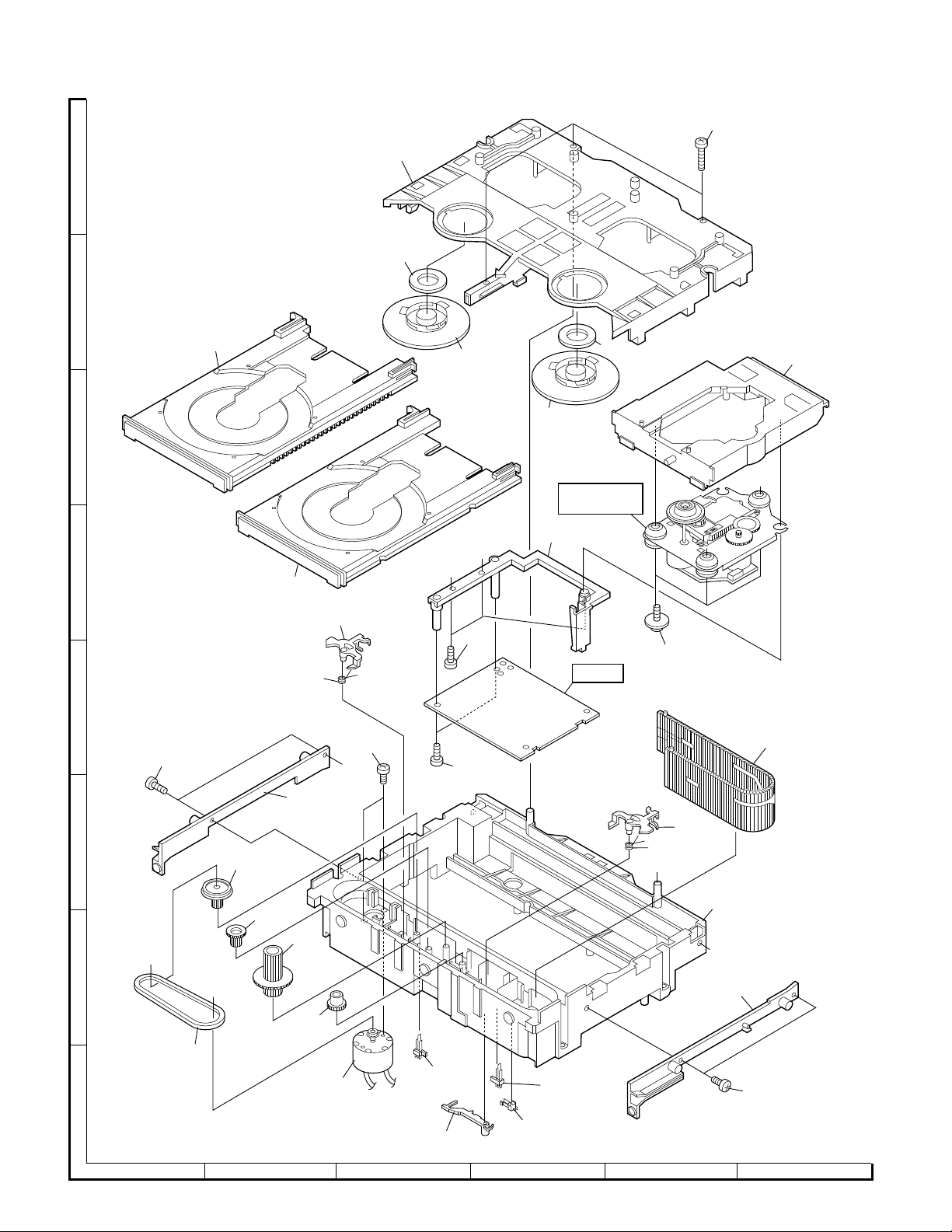
GX-CH170X/CH170Z
A
B
401x3
102
118
108
117
118
110
117
C
CD
MECHANISM
116
D
109
111
404x3
402x3
114
E
403x2
405x2
405x2
PWB-D
107
122
112
F
114
103
104
101
105
G
123
106
115
M981
SW982
H
113
1
2 3 4 5 6
SW981
SW983
405x2
Figure 9 CD CHANGER EXPLODED VIEW
– 9 –
Page 49

GX-CH170X/CH170Z
A
B
C
D
E
F
G
H
1
2 3 4 5 6
GX-CH170X
GX-CH170Z
619x3
619
618
241
254x2
PWB-A2
GX-CH170X
217-2
217-1
217-2
217-1
GX-CH170Z
201
604
605
201-1
201-2
619x3
217
618
619
217
PWB-A7
232
254x2
242
602x2
GX-CH170Z
ONLY
262
614
PWB-A6
253
604
605
PWB-A2
602
229
602
264
GX-CH170Z
ONLY
602
229
621
235
238
PWB-B
264
604
602x3
256x2
208
209
211
602x2
602x2
271
255
237
602
606
606
PWB-A5
236
268
206
209
602x4
201
233
609
207
227
PWB-B
603x4
LCD801
230
240
GX-CH170X
251
608
602x2
253
230
CNW2
205
204
607
604
203
608
PWB-A8
231
GX-CH170Z
GX-CH170X
603x2
601
602
226
611
PWB-B
606x6
269
602x5
248
252
234
602x3
612
250
GX-CH170Z
ONLY
622
263
270
PWB-A3
234
PWB-A4
PWB-A1
611
247
Silicon
Grease
CNW2
602x3
210
608x2
PWB-C
214
201-2
201-1
GX-CH170Z
TAPE
MECHANISM
219
220
221
222
265
223
228
224
608x2
608x2
228
225
213-1
213
-2
213
259
215
260
214-2
215
216x2
214-1
Figure 10 CABINET EXPLODED VIEW
– 10 –
Page 50

GX-CH170X/CH170Z
A
SP604(R-CH)
701-1
702-1
701
SP603(L-CH)
B
C
SP601(L-CH)
LINE
WHITE
702
SP602(R-CH)
SP603
SP604
D
SP601
706x4
SP602
708
E
F
G
704
703
H
1
2 3 4 5 6
707x4
Figure 11 SPEAKER BOX VIEW
– 11 –
Page 51

— M E M O —
GX-CH170X/CH170Z
– 12 –
Page 52

GX-CH170X/CH170Z
Writer and Editor: Quality & Reliability Control Center of Communication & Audio Systems Group, Sharp Corp.
A9606-2150NS•TI•M
Printed in Japan
EX • SA • SZ
 Loading...