

Sharp GP2W0106YP Datasheet

GP2W0106YP
IrDA Data Sheet
FEATURES
• Built-in Photodiode
• Operating voltage 2.0 V to 3.6 V
• Conforms to eye safety IEC60825-1, without external resistor
• This product shall not contain the following materials, and these materials shall not be used in the production process for this product.
–CFC
– Halon
– Carbon Tetrachloride
– 1.1.1. Trichloroethane (Methylchloroform)
– Specific brominated flame retardants such as the
INTRODUCTION
This specification applies to the outline and charac-
teristics of IrDA 1.2 type (data rate 2.4 kbps to
115.2 kbps, low power option compliant) optical data
communication transceiver.
NOTES
• Caution should be taken to prevent the detector surface from being smeared with dust or dirt, or from
being touched, as it may cause faulty operation.
• Cleaning conditions:
– Solvent cleaning: Solvent temperature 45°C or
– Ultrasonic cleaning: The effect of ultrasonic
– Cleaning solvent: The cleaning shall be carried
• In order to prevent electrostatic damage to the integrated circuit, handle this device in a static-free environment and workstation.
S
PBBO
less. Immersion for 3 minutes or less.
cleaning on the device differs by cleaning bath
size, ultrasonic power output, cleaning time, PCB
size or device mounting condition, etc. Test the
device under actual conditions and confirm that
ultrasonic cleaning does not cause any immediate or potential defects.
out with ethyl alcohol, methyl alcohol, or isopropyl
alcohol.
and PBBS are not used in this device.
S
115 kbps Transceiver
• External force applied to the device after mounting can
cause mounting defects such as the terminal coming
off. Be careful when handling the device and prevent
objects from touching the device after mounting.
• Refer to the ‘Precautions for Soldering’ section.
• When the system (program) is designed, the turn
around time from transmit to receive should be
designed by considering 200 µs or more that is specified by IrDA. This turn around time means the time
that this device does not temporarily detect the
incoming signal, since the transmitted light from the
transmitter side reaches the detector side of the
same transceiver.
• Consider that 200 µs or more (at T
signal) is necessary to return from shut-down mode
to ready-operation mode. In addition, thoroughly
confirm the operation in the actual application.
• When there is considerable external stray light or a
light source is located near the transceiver, or the
detector face receives considerable external stray
light, a pulse other than desired signal output may
be generated as noise on output terminal of the
transceiver. Consider the layout and structure in
your design to minimize disturbing light on the
detector face.
• When the sensor is adopted in an IR communication
system, it should be used according to the signal
method which is specified by ‘Serial Infrared Physical Layer Link Specification’ published by the Infrared Data Association. Faulty operation may occur, if
a signal method other than that specified is used.
• RXD pinout is a pullup (260 kΩ TYP.) to V
down mode. See Table 1 and Figure 2.
• In circuit designs, make allowance for the degradation
of the light emitting diode output that results from
long-term continuous operation (50% degradation/5
years). The light emitting diode output may be
degraded quickly when operated at T
fore it is recommended to operate over T
= 25°C, no input
A
in shut-
DD
= -40°C, there-
A
= -20°C.
A
IrDA Data Sheet 1
GP2W0106YP 115 kbps Transceiver
GP2W0106YP-2
TR1
TR2
260 kΩ
TYP.
RXD
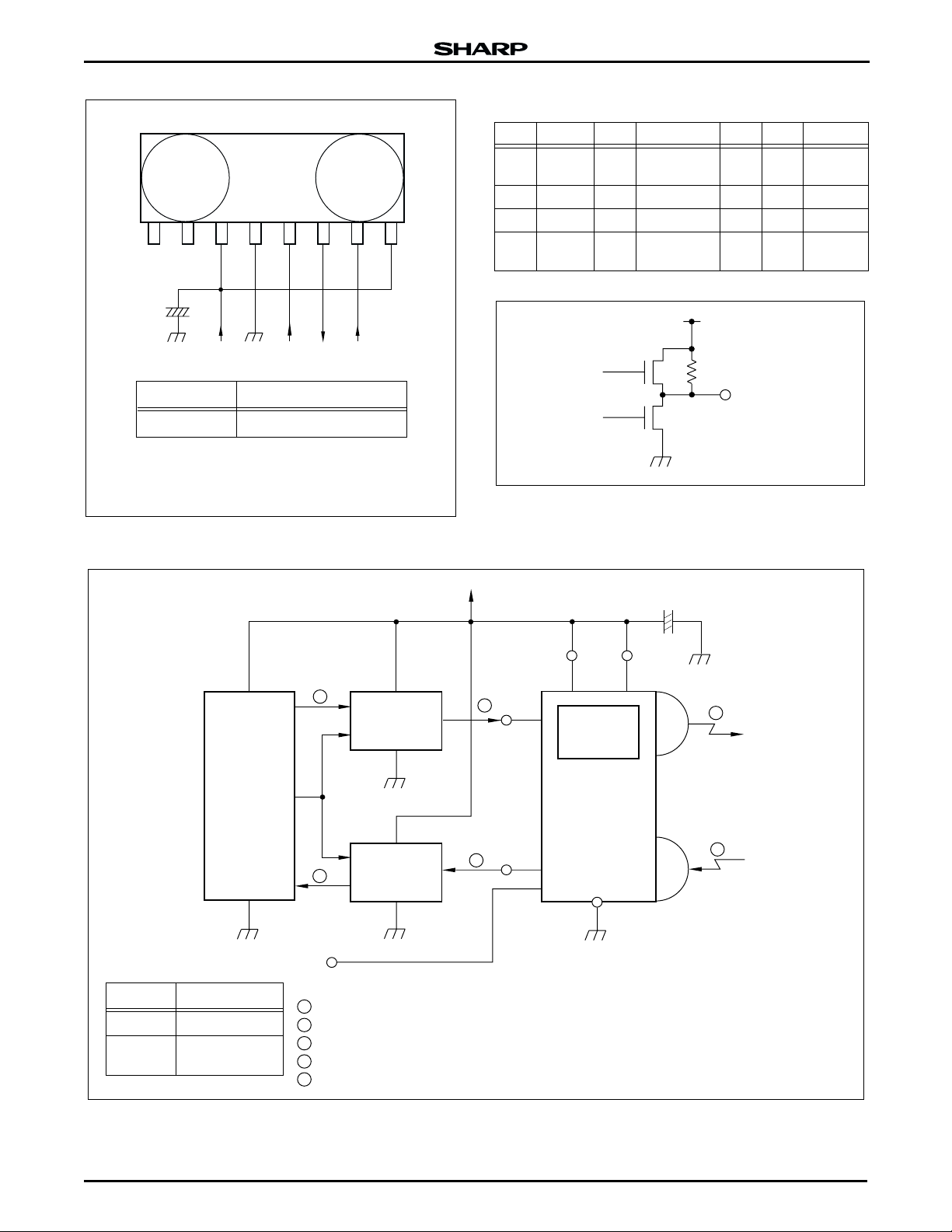
Table 1. I/O Truth Table
SD TXD LED RECEIVER TR1 TR2 RXD
Not
Valid
High
Pullup
1NC2NC3
V
+
CX
4
5SD6
GND SD RXD TXD
DD
GND
V
DD
RXD7TXD8LEDA
Low High On Don’t Care ——
Low Low Off IrDA Signal Off On Low
Low Low Off No Signal On Off High
High
Don’t
Care
Off Don’t Care Off Off
COMPONENT
CX 3.3 µF/6.3 V (NOTE 1)
NOTES:
1. Choose the most suitable CX according to the
noise level and noise frequency of power supply.
2. Pin 1 and Pin 2 are not connected internally.
RECOMMENDED VALUE
Figure 1. Recommended External Circuit
1
ENCODER
CIRCUIT
UART
GP2W0106YP-1
Figure 2. RXD Equivalent Circuit
CX
+
LEDA
2
TXD
CONSTANT
CURRENT
CIRCUIT
GP2W0106YP
V
DD
3
3
GP2W0106YP-3
SD INPUT PERFORMANCE
LOW Normal Mode
HIGH
Shutdown
Mode
4
5
NOTES:
1 Transmitting data waveform
2 Encoder circuit output waveform
3 Transmitter output optical signal waveform
4 GP2W0106YP receiver output waveform
Receiving data waveform
5
DECODER
CIRCUIT
RXD
SD
Figure 3. Example of Circuit
GND
2 IrDA Data Sheet
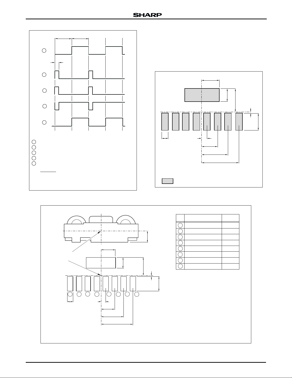
115 kbps Transceiver GP2W0106YP
1.425
1.55
0.475
2.375
3.325
1.55
0.1
1.1
2.0
NOTES:
1. Dimensions are in mm.
2. Dimensions are for reference.
3. Soldering paste area
GP2W0106YP-6
0.6
T
1
0
T
10 1
3T/16
2
3
4
5
0
10 1
NOTES:
1 Transmitting data waveform
2 Encoder circuit output waveform
3 Transmitter output optical signal waveform
4 GP2W0106YP receiver output waveform
5 Receiving data waveform
T =
1
Data Rate
Data rate: 2.4 kbps, 9.6 kbps, 19.2 kbps, 38.4 kbps,
57.6 kbps, 115.2 kbps
Figure 4. Example of Signal Waveform
Recommended Size of
Solder Cream Paste
Open the solder mask as shown in Figure 5. The
size of solder cream paste for this device before reflow
soldering must be as large as one of the foot pattern
land, indicated in Figure 6.
GP2W0106YP-4
Figure 5. Solder Cream Paste Size
NOTES:
1. Dimensions are in mm.
2. Dimensions are shown for reference.
3. Connect foot pattern of shield case to GND pattern.
IrDA Data Sheet 3
CENTER OF
MOUNTING AREA
8
0.6
7
6
5
0.475
1.0
1.55
1.425
4
2.375
3
3.325
1.1
2
2.0
0.1
1
Figure 6. Foot Pattern of PCB
1.55
PIN
1
2
3
4
5
6
7
8
PIN NAME SYMBOL
NC
NC
V
DD
Ground
Shutdown
Receiver Data Output
Transmitter Data Input
LED Anode
NC
NC
V
DD
GND
SD
RXD
TXD
LEDA
GP2W0106YP-5
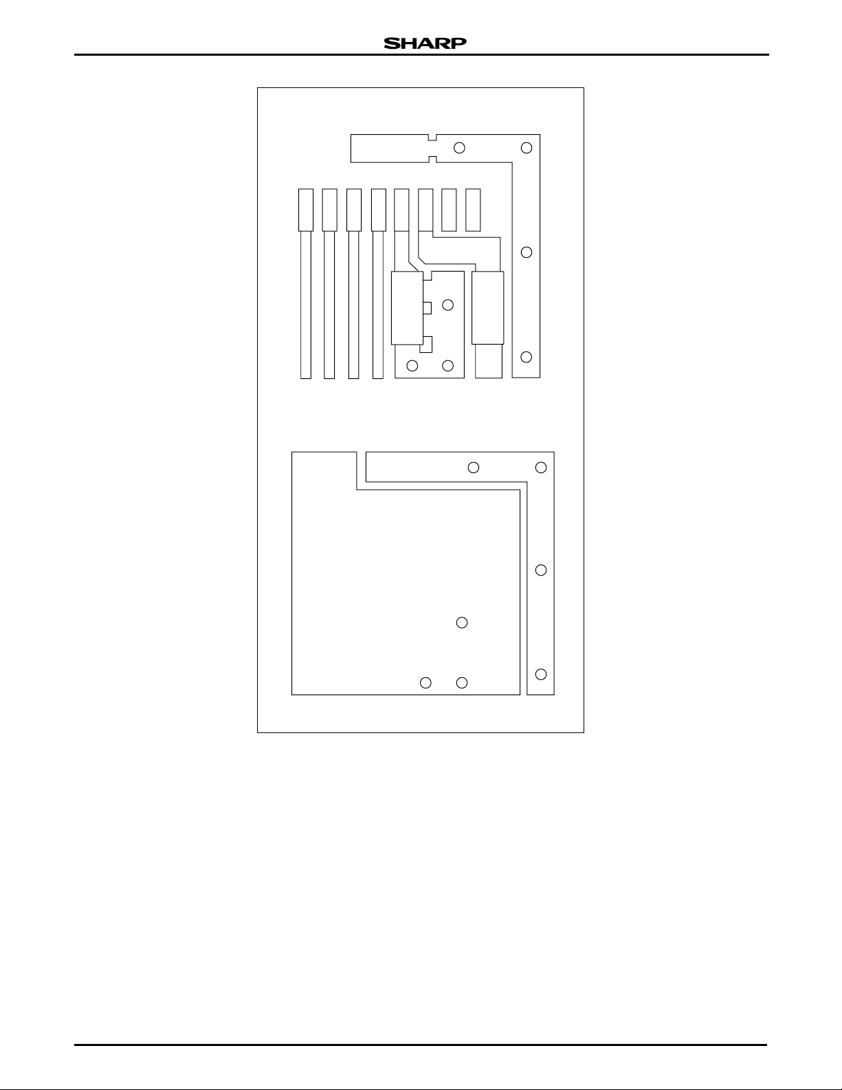
GP2W0106YP 115 kbps Transceiver
COMPONENT SIDE
CX
LEDA
TXD
RXD
SD
GND
CIRCUIT SIDE
Figure 7. PCB Layout Example
DD
V
GND
SHIELD
2W0106-7
4 IrDA Data Sheet
115 kbps Transceiver GP2W0106YP
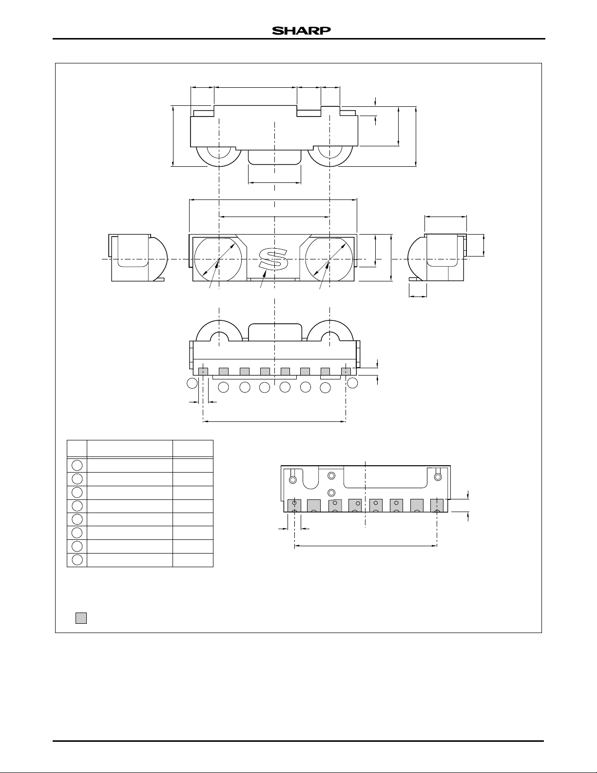
1.15 3.9
2.75 ±0.3
CENTER
OF DETECTOR
2.5
7.9 ±0.3
5.2
EMBOSSED
'S'
1.15 0.9
φ2.2φ2.2
CENTER
OF EMITTER
1.5 ±0.3
0.48
2.15 ±0.3
1.88
0.8
±0.3
2.7
+0.3
-0.2
2 ±0.3
1.05 ±0.3
PIN
1
2
3
4
5
6
7
8
PIN NAME SYMBOL
NC
NC
V
DD
Ground
Shutdown
Receiver Data Output
Transmitter Data Input
LED Anode
1
NC
NC
V
DD
GND
SD
RXD
TXD
LEDA
2 3
+0.2
8 - 0.4
-0.3
PO .95 x 7 = 6.65
8 - 0.6
5 6
4
BOTTOM VIEW
NOTES:
1. Dimensions are in mm.
2. Unspecified tolerances are ±0.2
3.
Adhesion of resin to the terminal area are allowed MAX. 0.2 mm.
area: Au plating
Figure 8. GP2W0106YP Outline Dimensions
8
7
PO .95 x 7 = 6.65
0.35
0.6
±0.3
GP2W0106YP-8
IrDA Data Sheet 5
 Loading...