

Page 1
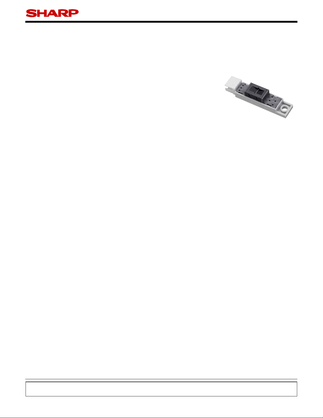
GP2A200LCS0F
Series
GP2A200LCS0F Series
Detecting Distance : 2 to 22mm
*
OPIC Output,
Refl ective Photointerrupter with
Connector
Description
■
GP2A200LCS0F Series
photointerrupters with emitter and detector facing the
same direction in a molding that provides non-contact
sensing. This family of devices uses light modulation to
reduce the affects of disturbing light, and the sensor is
optimized to work in the selected focal distance. A 3-pin
connector is included to allow remote-mount or off-board
designs.
Features
■
1. Refl ective with OPIC Light Modulated Output
2. Highlights :
• Includes additional screw fi xing holes
• Position pin to prevent mis-alignment
• Long focal distance
3. Key Parameters :
• Detecting distance : 2 to 22mm (White paper)
5 to 15mm (Black paper)
• Undetecting distance : over 90mm (White paper)
• Connector :
(PN : 292133-3)
(PN : 292133-3)
GP2A240LCS0F
(PN : 292133-3)
4. RoHS directive compliant
GP2A200LCS0F
GP2A200LCSCF
GP2A210LCSJF
(PN : 4-292133-3)
are OPIC output, reflective
; Tyco Electronics AMP K.K.
; Tyco Electronics AMP K.K.
; Tyco Electronics AMP K.K.
; Tyco Electronics AMP K.K
.
Agency approvals/Compliance
■
1. Compliant with RoHS directive
Applications
■
1. General purpose detection of paper presence or motion.
2. Example: PPC, FAX, Printer
* "OPIC"(Optical IC) is a trademark of the SHARP Corporation. An OPIC consists of a light-detecting element and a signal-
processing
Notice The content of data sheet is subject to change without prior notice.
In the absence of confi rmation by device specifi cation sheets, SHARP takes no responsibility for any defects that may occur in equipment using any SHARP
devices shown in catalogs, data books, etc. Contact SHARP in order to obtain the latest device specifi cation sheets before using any SHARP device.
Sheet No.: D3-A05101FEN
1
Date Jun. 30. 2005
© SHARP Corporation
Page 2
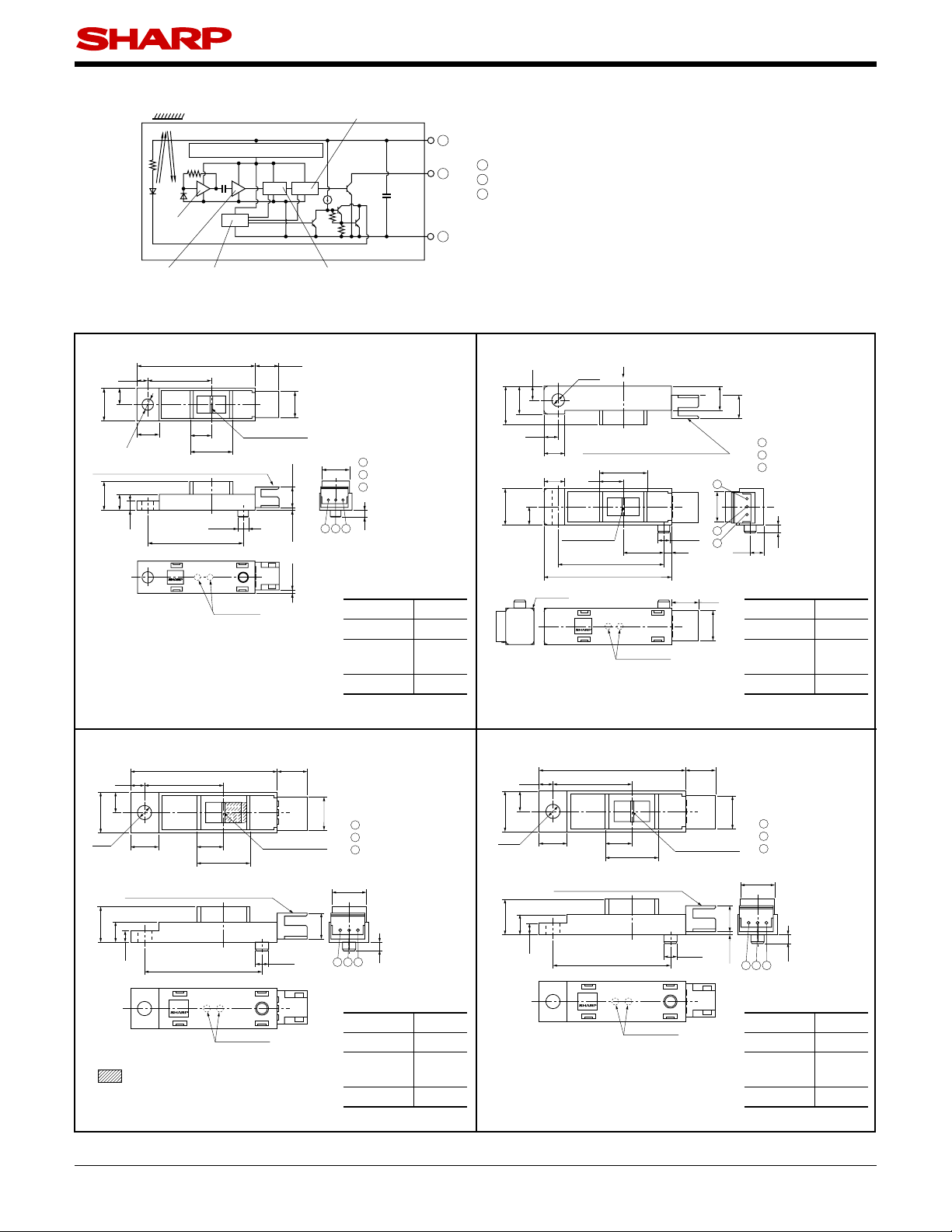
Internal Connection Diagram
■
GP2A200LCS0F Series
Reflective object
Voltage regulator
Amp.
Demodulator circuit
1
1
V
2
3
CC
V
OUT
GND
2
3
Comparator Oscillator circuit Sync. detecting circuit
Outline Dimensions
■
GP2A200LCS0F GP2A200LCSCF
3.1
4.5
9
6.2
φ3.2
Connector : 292133-3 (Tyco Electronics AMP. K. K)
8
4.5
2.5
17.7
33
26.5
6
12
φ3
0 7
+0
−0.2
Date code
Product mass : approx. 1.95g Product mass : approx. 2.3g
(6.8)
(7.8)
Optical center
(5.8)(0.65)(0.9)
1
V
7.8
1 2 3
2
3
2
CC
V
OUT
GND
• Unspecifi ed tolerance
shall be as follows ;
Dimensions
less than 6
6 or more
less than 14
14 or more
Tolerance
0.2
±
0.3
±
0.4
±
• *( ) : Reference dimensions
9.6
9
7
3.5
3.5
4.5
4-SR1
View A
φ3.2
Connector : 292133-3
5.2
(Tyco Electronics AMP K.K.)
6
View A
12
26.5
32
02
Date code
5.2
Optical center
10.2
(Unit : mm)
6.1
(5.8)
1
V
CC
2
V
OUT
3
GND
3
7.8
+0.0
2
φ3
−0.2
1
2
(6.8)
(7.8)
2
3.5
• Unspecifi ed tolerance
shall be as follows ;
Dimensions
less than 6
6 or more
less than 14
14 or more
Tolerance
0.2
±
0.3
±
0.4
±
• *( ) : Reference dimensions
GP2A210LCSJF
33
3.1
4.54.5
98
φ3.2
Connector : 4-292133-3 (Yellow)
(Tyco Electronics AMP K.K.)
2.5
17.7
26.5
66.2
12
99
Date code
Optical center
φ3
• : Portion Built-in IR-90 fi lter
Product mass : approx. 1.95g
(6.8)
+0.0
−0.2
(7.8)
1
V
CC
2
V
OUT
3
GND
7.8
(5 .8)
2
1 2 3
• Unspecifi ed tolerance
shall be as follows ;
Dimensions
less than 6
6 or more
less than 14
14 or more
Tolerance
±
±
±
• *( ) : Reference dimensions
0.2
0.3
0.4
GP2A240LCS0F
33
17.7
66.2
12
Connector : 292133-3
(Tyco Electronics AMP K.K.)
26.5
51
Date code
98
φ3.2
3.1
4.54.5
2.5
Product mass : approx. 1.95g
Connector terminal plating material : Sn
2
(6.8)
Optical center
+0.0
φ3
−0.2
(7.8)
1
V
CC
2
V
OUT
3
GND
7.8
(5 .8)(0.65)
2
1 2 3
• Unspecifi ed tolerance
shall be as follows ;
Dimensions
less than 6
6 or more
less than 14
14 or more
Tolerance
0.2
±
0.3
±
0.4
±
• *( ) : Reference dimensions
Sheet No.: D3-A05101FEN
Page 3

Date code (2 digit)
1st digit 2nd digit
Year of production Month of production
A.D. Mark Month Mark
2000 0 1 1
2001 1 2 2
2002 2 3 3
2003 3 4 4
2004 4 5 5
2005 5 6 6
2006 6 7 7
2007 7 8 8
2008 8 9 9
2009 9 10 X
2010 0 11 Y
: : 12 Z
repeats in a 10 year cycle
GP2A200LCS0F Series
Country of origin
Japan
3
Sheet No.: D3-A05101FEN
Page 4

Absolute Maximum Ratings
■
Parameter Symbol Rating Unit
Supply voltage V
Output voltage V
*1
Output current I
*2
Operating temperature T
*2
Storage temperature T
∗
1 Sink current refer to
∗
2 The connector should be plugged in/out at normal temperature.
Electro-optical Characteristics
■
Fig.5.
CC
O
OL
opr
stg
Parameter Symbol Condhitions MIN. TYP. MAX. Unit
Supply voltage V
Current dissipation (I) I
*3
Current dissipation (II) I
Low level output voltage V
High level output voltage V
*4
Non detection distance
GP2A210LCSJF
*4
Detection distance
*5
Response time
*6
Acceptable illuminance
∗
3 Refer to Fig.1.
∗
4 Refer to Fig.2.
∗
5 Refer to Fig.3.
*
6 Refer to Fig.4.
CC
CC
CCP
OL
OH
L
LHL
L
HLS
L
HLL
t
PLH
t
PHL
Ev1
Ev2 1 500
(T
25˚C)
=
a
0.5 to +7V
−
30 V
50 mA
10 to +70 ˚C
−
20 to +80 ˚C
−
Smoothing value V
Pulse peak value V
V
5V, I
=
CC
5V, R
V
=
CC
=
OL
=1kΩ
L
KODAK Gray Cards, V
KODAK Gray Cards, V
Black paper, V
KODAK Gray Cards , V
Black paper, V
−
5V, R
CC
=
=∞−−
L
5V
=
CC
16mA, at detecting time
, at non detecting time 4.5
5V
=
CC
5V
=
CC
5V
=
CC
5V 22
=
CC
5V 15
=
CC
5V
V
=
CC
−
GP2A200LCS0F Series
4.75
−
−−
−−
−−
−−
−−
−−
−−
−−
−−
−−
−−
3 000
−−
−−
25˚C)
(T
=
a
5.25 V
30 mA
150 mA
0.4 V
V
90
70
2
5
mm
mm
mm
1ms
1ms
lx
lx
Refl ective object Black paper (black) : Standard refl ective object (provided by SHARP Corporation)
KODAK Gray Cards (use the white side refl ects about 90%)
: Standard refl ective object (provided by SHARP Corporation)
PPC paper : Standard refl ective object (provided by SHARP Corporation)
4
Sheet No.: D3-A05101FEN
Page 5

GP2A200LCS0F Series
Fig.1 Test Condition for Peak Pulse Value I
R=1Ω
1
V
2
3
R
V
CC
=1kΩ
L
V
O
GND
=5V
CCP
t
W
t
P
I
CCP=Vr
(TYP.)=8μs (GP2A240LCS0F : 2.5 to 9.3μs)
t
W
(TYP.)=130μs (GP2A240LCS0F : 40 to 150μs)
t
P
Photointerrupter
Fig.2 Test Condition for Detecting Distance Characteristics
Reflective object
Detection surface
V
O
Output V
OH
V
OL
Detecting distance L
L
HLS
L
LHS
L
HLL
L
LHL
/1Ω
r
V
Fig.3 Test Circuit for Response Time
Reflective object
Detection surface
L
=1kΩ
R
L
1
2
3
Photointerrupter
V
CC
V
O
GND
=5V
t
PHL
V
OUT
waveform
With reflective object
t
PLH
V
OH
1.5V
V
OL
Without reflective object
Fig.4 Test Condition for External Disturbing Light Illuminance
EV1 : At non-detecting EV2 : At detecting
Emission/detection
surface
Light source A
Photointerrupter
Illuminance shall be that on the emission/detection surface.
Output shall not go from "H" to "L".
Light source A
PPC paper
Emission/detection surface
Photointerrupter
Illuminance shall be that on the reflective
object.
Output shall not go from "L" to "H".
15mm
5
Sheet No.: D3-A05101FEN
Page 6

GP2A200LCS0F Series
Fig.5 Output Current vs.
Ambient Temperature
50
40
(mA)
OL
30
20
Output Current I
10
0
−100 25507570 100
Ambient temperature T
a
(C)
Fig.7 Low Level Output Voltage vs.
Low Level Output Current
VCC=5V
At detecting
(V)
OL
0.1
Fig.6 Low Level Output Voltage vs.
Ambient Temperature
0.3
(V)
OL
0.2
0.1
Low level output voltage V
0
−100 10203040506070
Fig.8
Dissipation Current(Smoothing Value)
IOL=30mA
Ambient temperature Ta (C)
VCC=5V
At detecting
16mA
5mA
vs. Ambient Temperature
(mA)
CC
7
6
5
4
Ta=−10˚C
25˚C
70˚C
3
2
Low level output voltage V
0.01
1 10 100
Low level output current I
OL
(mA)
Dissipation current I
1
0
4.75 4.85 4.95 5.05 5.15 5.25
Supply voltage V
(V)
CC
Remarks : Please be aware that all data in the graph are just for reference and not for guarantee.
6
Sheet No.: D3-A05101FEN
Page 7

Design Considerations
■
●
Design guide
1) VO terminal : Open collector output
This product operates the light emitter by pulse drive. Please supply the stable supply voltage in order to
prevent error operation by pulse current.
Please use this device after connecting a capacitor between V
2) Prevention of detection error
Please be careful that you need to keep the direct inverter light away from the photo detecting surface
since the device will not operate correctly in such case.
In addition, we recommend to make sure the operation test in the actual application.
3) Plugging in/out
The connector should be plugged in/out at normal temperature.
This product is not designed against irradiation and incorporates non-coherent IRED.
●
Parts
This product is assembled using the below parts.
GP2A200LCS0F Series
and GND for prevention of line noise.
O
• Photodetector (Q'ty : 1)
Category
Phototransistor 900 700 to 1 200 400
Maximum Sensitivity
wavelength (nm)
[Using a silicon photodiode as light detecting portion, and a bipolar IC as signal processing circuit]
Sensitivity
wavelength (nm)
• Photo emitter (Q'ty : 1)
Category Material
Infrared emitting diode
(non-coherent)
Gallium arsenide (GaAs) 950 0.3
Maximum light emitting
wavelength (nm)
• Material
Case Lens Bottom cover
GP2A200LCS0F
GP2A200LCSCF
GP2A210LCSJF
GP2A240LCS0F
∗
Black polyphernylene
Sulfi de resin (UL94 V-0)
Polycarbonate resin
(UL94 V-2)
Response time (μs)
I/O Frequency (MHz)
Polycarbonate resin (Gray)
(UL94 V-2)
Polycarbonate resin (Navy Blue)
(UL94 V-2)
The IR-90 fi lter (Fuji Photo Film Co., Ltd.) is inserted between case and detector side lens.
∗
• Others
Laser generator is not used.
7
Sheet No.: D3-A05101FEN
Page 8

Manufacturing Guidelines
■
●
Cleaning instructions
Polycarbonate resin is used as the material of the lens surface. So this product shall not be cleaned by
cleaning solvent absolutely. Dust and stain shall clean by air blow, or shall clean by soft cloth.
●
Presence of ODC
This product shall not contain the following materials.
And they are not used in the production process for this product.
Regulation substances : CFCs, Halon, Carbon tetrachloride, 1.1.1-Trichloroethane (Methylchloroform)
Specifi c brominated fl ame retardants such as the PBBOs and PBBs are not used in this product at all.
This product shall not contain the following materials banned in the RoHS Directive (2002/95/EC).
•Lead, Mercury, Cadmium, Hexavalent chromium, Polybrominated biphenyls (PBB), Polybrominated
diphenyl ethers (PBDE).
GP2A200LCS0F Series
8
Sheet No.: D3-A05101FEN
Page 9

Package specifi cation
■
●
Case package
Package materials
Anti-static plastic bag : Polyethtylene
Moltopren : Urethane
Packing case : Corrugated fi berboard
Package method
100 pcs of products shall be packaged in a plastic bag, Ends shall be sealed by stapler. The bottom ot the
packing case is covered with moltopren, and 2 plastic bags shall be put int the packing case.
Moltopren should be located after all product are settled (1 packing conteains 200 pcs).
Packing composition
GP2A200LCS0F Series
Moltopren
plastic bag
Packing case
9
Sheet No.: D3-A05101FEN
Page 10

Important Notices
■
· The circuit application examples in this publication
are provided to explain representative applications of
SHARP devices and are not intended to guarantee any
circuit design or license any intellectual property rights.
SHARP takes no responsibility for any problems related
to any intellectual property right of a third party resulting
from the use of SHARP's devices.
· Contact SHARP in order to obtain the latest device
specification sheets before using any SHARP device.
SHARP reserves the right to make changes in the
specifi cations, characteristics, data, materials, structure,
and other contents described herein at any time
without notice in order to improve design or reliability.
Manufacturing locations are also subject to change
without notice.
· Observe the following points when using any devices
in this publication. SHARP takes no responsibility for
damage caused by improper use of the devices which
does not meet the conditions and absolute maximum
ratings to be used specifi ed in the relevant specifi cation
sheet nor meet the following conditions:
(i) The devices in this publication are designed for use
in general electronic equipment designs such as:
--- Personal computers
--- Offi ce automation equipment
--- Telecommunication equipment [terminal]
--- Test and measurement equipment
--- Industrial control
--- Audio visual equipment
--- Consumer electronics
(ii) Measures such as fail-safe function and redundant
design should be taken to ensure reliability and safety
when SHARP devices are used for or in connection
GP2A200LCS0F Series
with equipment that requires higher reliability such as:
--- Transportation control and safety equipment (i.e.,
aircraft, trains, automobiles, etc.)
--- Traffi c signals
--- Gas leakage sensor breakers
--- Alarm equipment
--- Various safety devices, etc.
(iii) SHARP devices shall not be used for or in
connection with equipment that requires an extremely
high level of reliability and safety such as:
--- Space applications
--- Telecommunication equipment [trunk lines]
--- Nuclear power control equipment
--- Medical and other life support equipment (e.g.,
scuba).
· If the SHARP devices listed in this publication fall
within the scope of strategic products described in the
Foreign Exchange and Foreign Trade Law of Japan, it
is necessary to obtain approval to export such SHARP
devices.
· This publication is the proprietary product of SHARP
and is copyrighted, with all rights reserved. Under
the copyright laws, no part of this publication may be
reproduced or transmitted in any form or by any means,
electronic or mechanical, for any purpose, in whole or in
part, without the express written permission of SHARP.
Express written permission is also required before any
use of this publication may be made by a third party.
· Contact and consult with a SHARP representative
if there are any questions about the contents of this
publication.
[H176]
10
Sheet No.: D3-A05101FEN
 Loading...