

Page 1
GP1S56T
GP1S56T
Compact, High Sensing Accuracy
Type Photointerrupter with
Positioning Pin
■ Features
1. High sensing accuracy (Slit width : 0.15mm
2. Compact (Case height : 7.5mm
)
3. With positioning pin
4. PWB direct mounting type
■ Applications
1. Floppy disk drives
2. VCRs, cassette decks
3. Optoelectronic switches
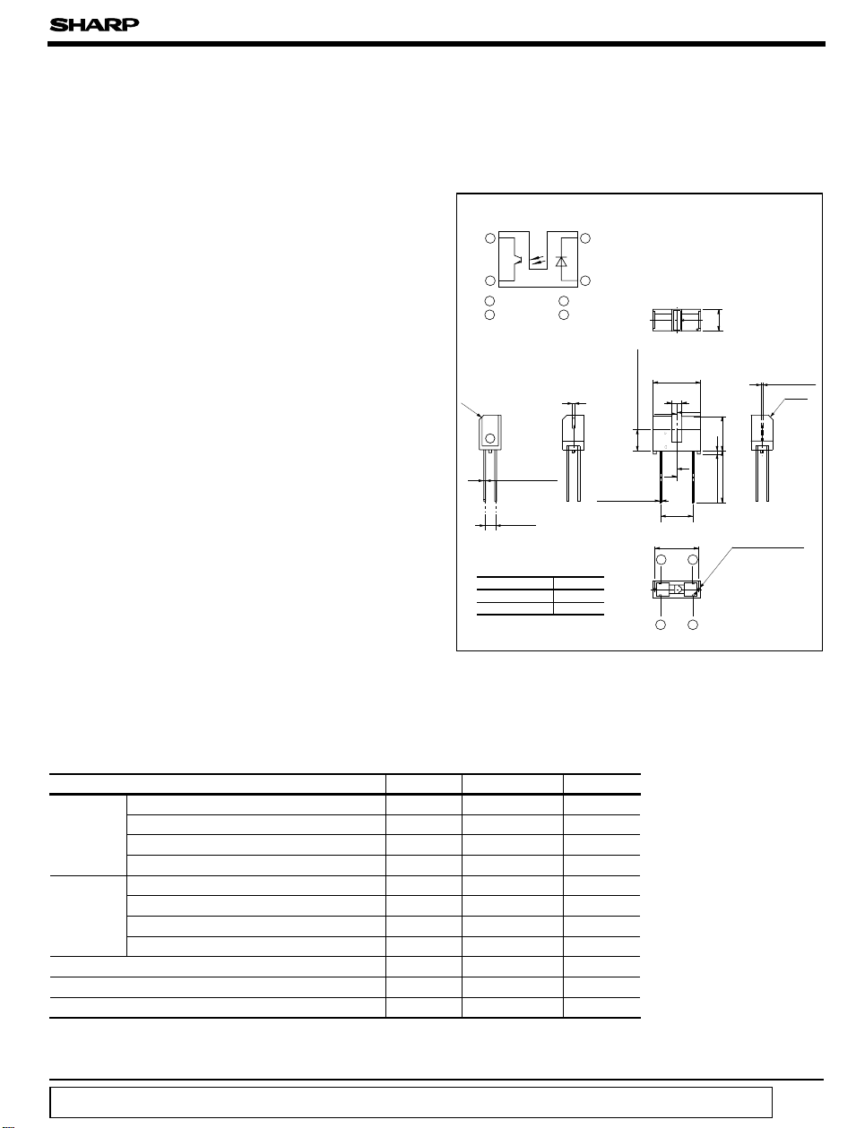
■ Outline Dimensions
)
Internal connection
diagram
32
14
1 Anode
2 Cathode
C1
0 - 4.5
(
2.54
* Unspecified tolerances
shall be as follows ;
Dimensions(d)Tolerance
d<=6.0 ± 0.1
6.0< d<=18.0 ± 0.2
* ( ): Reference dimensions
A-A’ section
(
Slit width of
emitter side
0.15
+ 0.3
- 0.1
)
3 Collector
4 Emitter
+ 0.07
- 0.07
4 - 0.4
)
11.0
2.0
A
Detector center
)
5.5
(
A’
+ 0.3
- 0
(
7.4
10.2
4
(
Unit : mm
56
S
5.0
+ 0.3
- 0
B
MAX.
B’
±
MIN.
2 - 0.7
)
0.15
2- φ 0.7
1
23
B-B’ section
(
Slit width of
detector side
7.5
12.0
0.15
C1.0
±
0.05
)
)
±
0.07
■ Absolute Maximum Ratings
(
Ta= 25˚C
)
Parameter Symbol Rating Unit
Input
Forward current I
*1
Peak forward current I
Reverse voltage V
F
FM
R
50 mA
1A
6V
Power dissipation P 75 mW
Collector-emitter voltage V
Output
Emitter-collector voltage V
Collector current I
Collector power dissipation P
Operating temperature T
Storage temperature T
*2
Soldering temperature T
*1 Pulse width<=100 µs, Duty ratio= 0.01
*2 For 5 seconds
“ In the absence of confirmation by device specification sheets, SHARP takes no responsibility for any defects that occur in equipment using any of SHARP's devices, shown in catalogs,
data books, etc. Contact SHARP in order to obtain the latest version of the device specification sheets before using any SHARP's device.”
CEO
ECO
C
C
opr
stg
sol
35 V
6V
20 mA
75 mW
- 25 to + 85 ˚C
- 40 to + 100 ˚C
260 ˚C
Page 2
GP1S56T
■ Electro-optical Characteristics
Parameter
Forward voltage
Input
Output
Transfer
characteristics
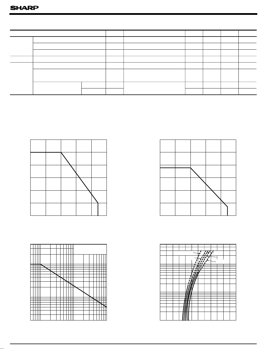
Fig. 1 Forward Current vs.
Ambient Temperature
60
50
)
mA
(
40
F
30
Peak forward voltage
Reverse current
Collector dark current
Collector Current Ic
Collector-emitter
saturation voltage
Response time
Rise time
Fall time
(
Ta = 25˚C
Symbol Conditions MIN. TYP. MAX. Unit
- 1.2 1.4 V
-34V
--10µA
-
nA1 100
0.4 - - mA
- - 0.4 V
-3890µs
- 48 110 µ s
V
V
V
FM
I
R
I
CEO
CE(sat
t
t
= 20mA
I
F
r
r
F
= 0.5A
I
FM
=3V
V
R
= 20V
V
CE
= 5V, IF= 20mA
V
CE
= 40mA
I
F
)
= 0.25mA
I
C
V
= 2V, IC= 0.5mA
CE
=1KΩ
R
L
Fig. 2 Collector Power Dissipation vs.
Ambient Temperature
120
)
100
mW
(
C
80
75
60
)
20
Forward current I
10
0
- 25 0 25 50 75 85 100
Ambient temperature Ta (˚C
Fig. 3 Peak Forward Current vs.
Duty Ratio
Pulse width <= 100µs
10
Duty ratio
Ta= 25˚C
-1
2000
)
mA
1000
(
FM
500
200
100
Peak forward current I
50
20
-2
52525
10
40
20
Collector power dissipation P
0
)
- 25 0 25 50 75 85 100
Ambient temperature Ta (˚C
)
Fig. 4 Forward Current vs.
Forward Voltage
500
T
75˚C
=
200
)
100
mA
(
50
F
20
10
Forward current I
5
2
1
1
0
a
50˚C
Forward voltage VF (V
25˚C
)
0˚C
-
25˚C
32.521.510.5
Page 3
GP1S56T
Fig. 5 Collector Current vs.
Forward Current
5
4
)
mA
(
C
3
2
Collector current I
1
0
10 20 30 40 50
0
Forward current I
Fig. 7 Collector Current vs.
Ambient Temperature
1.4
1.2
)
1.0
mA
(
C
0.8
0.6
(mA
F
V
=5V
CE
Ta= 25˚C
)
Fig. 6 Collector Current vs.
Collector-emitter Voltage
3.0
= 25˚C
T
a
2.5
)
mA
(
2.0
C
1.5
= 50mA
I
F
40mA
30mA
1.0
Collector current I
0.5
0
054321
Collector-emitter voltage VCE (V
20mA
10mA
78 9106
)
Fig. 8 Collector-emitter Saturation Voltage vs.
Ambient Temperature
0.20
I
= 40mA
F
I
)
V
(
)
sat
(
CE
V
0.15
= 0.6mA
C
0.4
Collector current I
0.2
0
025- 25 50 10075
Ambient temperature Ta (˚C
Fig. 9 Response Time vs.
Load Resistance
1000
500
100
)
50
µ s
(
10
5
Response time
1
0.5
0.1
0.1 1
t
f
t
d
Load resistance R
Collector-emitter saturation voltage
0.10
)
VCE=2V
I
= 0.5mA
C
= 25˚C
T
t
r
t
s
a
Input R
D
025-25
Ambient temperature Ta (˚C
50 10075
)
Test Circuit for Response Time
V
CC
R
L
Output
Output
Input
t
d
t
s
t
r
10%
90%
t
f
100010010
)
(kΩ
L
Page 4
GP1S56T
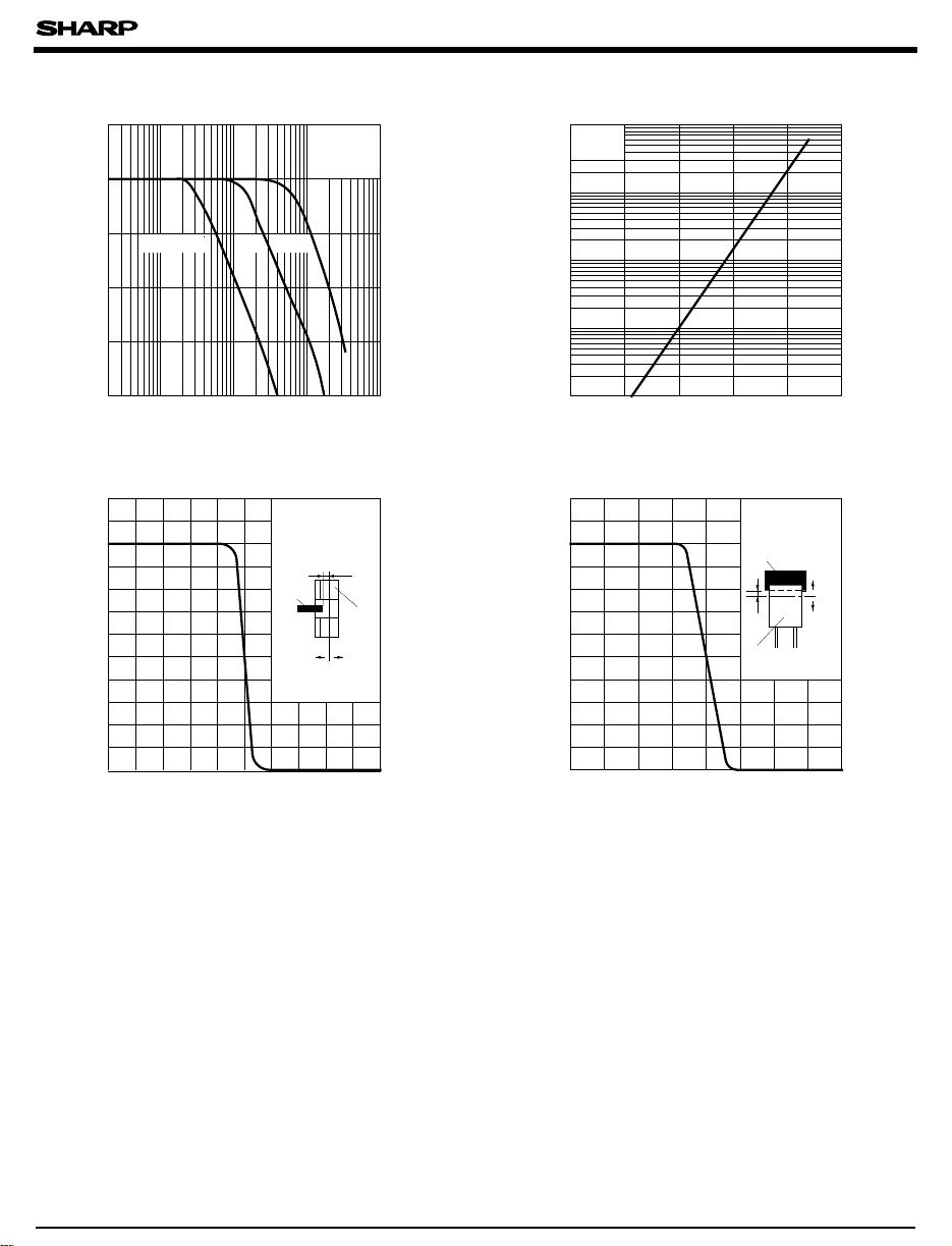
Fig.10 Frequency Response Fig.11 Collector Dark Current vs.
Ambient Temperature
-6
10
=
V
CE
5
20V
2
)
A
-7
(
10
5
CEO
2
-8
10
5
2
-9
10
Collector dark current I
5
2
-10
10
Ambient temperature T
7550 100250-25
)
(˚C
a
0
)
dB
(
-5
RL= 10kΩ
-10
Voltage gain Av
-15
-20
100Ω
1kΩ
3
10
4
252 5 25 25
10
Frequency f (Hz
10
)
V
CE
I
C
T
a
5
=2V
= 0.5mA
= 25˚C
6
10
Fig.12 Relative Collector Current vs. Fig.13 Relative Collector Current vs.
Shield Distance (1
100
)
%
(
50
Relative collector current
)
IF= 20mA
V
CE
T
a
Shield
(
Detector center
=5V
= 25˚C
L
Detector
-+
0
Shield Distance (2
100
)
%
(
50
)
Relative collector current
)
= 20mA
I
F
V
=5V
CE
= 25˚C
T
a
Shield
L
Detector
)
0
+
Detector center
(
0
- 0.5
- 0.4 - 0.3 - 0.2 - 0.1
Shield distance L (mm
0 0.1 0.2 0.3 0.4 0.5
)
■ Precautions for Use
(1)
In case of cleaning, use only the following type of cleaning solvent.
Ethyl alcohol, methyl alcohol, isopropyl alcohol
(2)
As for other general cautions, refer to the chapter “ Precautions for Use .”
0
- 1.0 1.0
Shield distance L (mm
)
2.00- 2.0
 Loading...