


Optical Mini-Jack for Digital
GP1F361T/GP1F361R
Audio Equipment
GP1F361T/GP1F361R
■ Features
1. Electric and optical signal compatible design
(Three kinds of terminals are
integrated into a single unit.
)
2. Compact design with small jack
compatible mini-plug
3. OPIC type
(Direct interface to microcomputer
of the I/O signals
(High fidelity real sound reproduction
)
)
4. High speed data transmission
Signal transmisson speed: MAX. 8Mbps
(
NRZ signal
5. Low voltage drive (2.7V to 3.6V
)
)
■ Applications
1. MD, DCC
2. Portable CD, DAT
■ Outline Dimensions
3 - 0.5
2.54
7.2
10
φ 3.6
3.7 3.7
9.65
4
5
6
2
7.0 4.0
1
789
Jack terminal configuration
GP1F361T GP1F361R
1
4
6
2
3
5
Drive
8 Vcc
7 Vin
IC
9 GND
8.7
6.72.3
3 - 1.5
LED
2.54
3.3
5.05
1.85
3
2
1
6.1
2.5
φ 6
(
Unit : mm
18.1
8 - 1.0
11.0
1
2
3
Jack terminal
4
5
6
7
8
Device terminal
9
OPIC light detector
)
2.8
1
4
6
2
3
5
7 Vcc
9 Vout
8 GND
∗ OPIC is a trademark of Sharp and stands for Optical IC.
It has light detecting element and signal processing circuitry
integrated single chip.
“ In the absence of confirmation by device specification sheets, SHARP takes no responsibility for any defects that occur in equipment using any of SHARP's devices, shown in catalogs,
data books, etc. Contact SHARP in order to obtain the latest version of the device specification sheets before using any SHARP's device.”

■ Absolute Maximum Ratings
GP1F361T/GP1F361R (Photoelectric conversion element
Parameter Symbol Rating Unit
Supply voltage V
()
Output current
Input voltage
GP1F361R
()
GP1F361T
Operating temperature T
Storage temperature T
∗1
Soldering temperature
CC
I
OH
I
OL
V
in
opr
stg
T
sol
)
- 0.5 to + 7.0 V
2 (source current
10 (sink current
- 0.5 to VCC+5.0 V
- 20 to + 70 ˚C
- 30 to + 80 ˚C
260 ˚C
GP1F361T/GP1F361R
)
)
mA
mA
GP1F361T/GP1F361R (Jack
)
Parameter Symbol Rating Unit
Total power dissipation P
Isolation voltage V
Operating temperature T
Storage temperature T
∗1
Soldering temperature T
∗1 5s/time up to 2 times.
tot
iso
opr
stg
sol
D.C.12V, 1A A.C. 500V
(
For 1min.
rms
)
- 20 to 70 ˚C
- 30 to 80 ˚C
260 ˚C
■ Recommended Operating Conditions
GP1F361T
Parameter Symbol MIN. TYP. MAX. Unit
Supply voltage
V
CC
2.7 3.0 3.6
Operating transfer rate T - - 8
GP1F361R
Parameter Symbol MIN. TYP. MAX. Unit
Supply voltage V
CC
2.7 3.0
Operating transfer rate T 0.1 - 8
Receiver input optical
power level
P
C
- 24.0 - - 14.5 dBm
■ Electro-optical Characteristics
GP1F361T (Photoelectric conversion element
Parameter Symbol Conditions MIN. TYP. MAX. Unit
Peak emission wavelength λ
Optical power output
couple with fiber
Supply current I
High level input voltage V
Low level input voltage V
Low→High delay time
High→Low delay time
Pulse width distortion
Jitter
)
P
P
C
CC
iH
iL
t
PLH
t
PHL
∆tw Refer to Fig. 3 - ns
∆tj Refer to Fig. 3 - 1 ns
Refer to Fig. 1 - 21 - 17 - 15 dBm
Refer to Fig. 2 -
Refer to Fig. 2 - - V
Refer to Fig. 2 - - 0.8 V
Refer to Fig. 3 - - ns
Refer to Fig. 3 - - ns
-
V
Mbps
3.6 V
Mbps
630 660 690 nm
812
2.1
-30
(
Ta= 25˚C
180
180
+30
30
)
mA
GP1F361T/GP1F361R
GP1F361R(Photoelectric conversion element
Parameter
Peak sensitivity
wavelength
Supply current
High level output voltage
Low level output voltage
Rise time
Fall time
Low→High delay time
High→Low delay time
Pulse width distortion
= - 14.5dBm
P
Jitter
C
= - 24dBm
P
C
Symbol Conditions MIN. TYP. MAX. Unit
λ
P
I
CC
V
OH
V
OL
t
r
t
f
t
PLH
t
PHL
∆tw Refer to Fig. 5 - 30 - + 30 ns
∆tj Refer to Fig. 6
)
-
-
Refer to Fig. 4 - mA
Refer to Fig. 5 - V
2.1
Refer to Fig. 5 0.4 V
Refer to Fig. 5 - 30 ns
Refer to Fig. 5 - 30 ns
Refer to Fig. 5 - - ns
Refer to Fig. 5 - - ns
700
12
-
-
-
17
5
- 1 30 ns
- - 30 ns
■ Mechanical and Electrical Characteristics
GP1F361T/GP1F361R (Jack
Parameter Symbol Conditions
Insertion force,
Withdrawal force
Contact resistance
Isolation resistance R
Note) This jack is designed for appliacable to φ 3.5 compact single head plug (EIAJ RC-6701A).
∗2 Measuring method of insertion force and withdrawal force.
Insertion and withdrawal force shall be measured after inserting and withdrawing 3 times by using EIAJ RC-6701A standard
plug for test.
∗3 Measuring method of contact resistance.
About movable contact terminal and make contacts, it measures at 100mA or less and 1000H
EIAJ 6701A standard plug for test.
)
F
P
Rcon ∗3
ISO
∗2
D.C. 500V,
1min.
MIN. TYP. MAX. Unit
5 - 35 N
- - 30 mΩ
100 - - MΩ
at the condition of inserting
Z
(
Ta = 25˚C
)
-nm
15
180
180
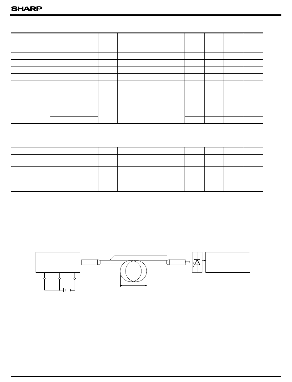
Fig. 1 Measuring Method Optical Output Coupling Fiber
Standard optical fiber cable
GP1F361T Unit
to be measured
Vin V
(1)
V
Note)
; 3.0V ±0.05V (State of operating
CC
(2)
To bundle up the standard fiber optic cable, make it into a loop with the diameter D= 10cm or more.
(The standard fiber optic cable will be specified elsewhere.)
GND
CC
V
CC
)
D
Optical power
meter
(
Anritsu) ML93B
The optical power meter
must be calibrated to
have the wavelength
sensitivity of 660nm.
(
0dB= 1mW
)
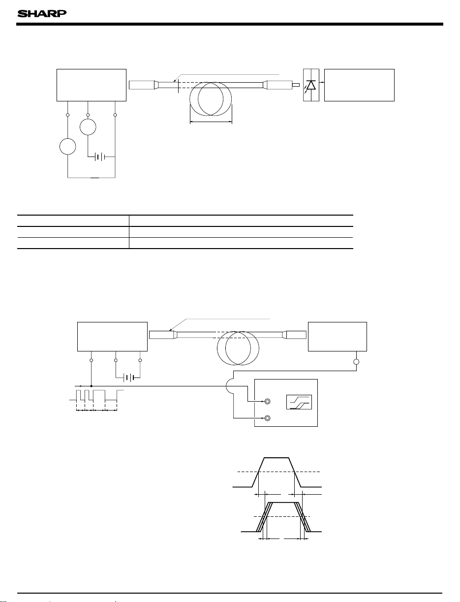
Fig. 2 Measuring Method of Input Voltage and Supply Current
GP1F361T/GP1F361R
Standard fiber optic cable
GP1F361T Unit
to be measured
Vin GND
Vcc
D
Vin
Icc
VCC
Input conditions and judgement method
Conditions
Vin= 2.1V or more
V
= 0.8V or less
in
Note) VCC= 3.0 ±0.05V (State of operating
-21<=P
<= -36dBm, ICC=12mA or less
P
C
)
Judgement method
<= -15dBm, ICC=12mA or less
C
Fig. 3 Measuring Method of Pulse Response and Jitter
Standard fiber optic cable
GP1F361T Unit
to be measured
Vin GND
Vcc
Vcc
Input
1
100
Input signal 3Mbps
biphase mark PRBS signal
Oscilloscope
CH1
CH2
Optical power
meter
(
Anritsu) ML93B
The optical power meter
must be calibrated to
have the wavelength
sensitivity of 660nm.
(
0dB= 1mW
)
Standard
receiver
Output
signal
Tektronix 7834
or 7934 type
Trigger ; CH1
Storage mode
Input signal
Standard receiver
output
t
PLH
∆ tjr ∆ tjf
50%
t
PHL
50%
Test item
Test item
Low→High pulse delay time
High→Low pulse delay time
Pulse width distortion
Low→High Jitter
High→Low Jitter
(1)
Notes
Fig. 4 Supply Current
The waveform write time shall be 4 seconds. But do not allow the waveform to be distorted by increasing the
brightness too much.
(2)
= 3.0 ±0.05V (State of operating
V
CC
(3)
The probe for the oscilloscope must be more than 1MΩ and less than 10pF.
Supply voltage VCC= 3.0 ± 0.05V
Symbol Test condition
t
PLH
t
PHL
∆tw
∆tjr
∆tjf
)
∆tw = t
PHL-tPLH
Set the trigger on the rise of input signal
to measure the jitter of the rise of output
Set the trigger on the fall of input signal
to measure the jitter of the fall of output
Input conditions
GP1F361T/GP1F361R
-
-
Measuring method
Optical output
coupling fiber
Standard transmitter
input signal
Standard
transmitter
Vin GND
Vcc Vcc
Input
5V
= -14.5dBm
P
C
6Mbps NRZ, Duty50 % or 3Mbps
biphase mark PRBS signal
fiber optic cable
Fig. 5 Measuring Method of Output Voltage and Pulse Response
fiber optic cable
Standard
transmitter
Vin Vcc GND
5V
Input
6Mbp/s NRZ, duty 50%
GP1F361R
Unit to be measured
GND Vout
Vcc
A
Ammeter
GP1F361R
Unit to be measured
GND Vout
Vcc
Vcc
CH1
CH2
Measured on an ammeter
(
DC average amperage
Tektronix 7834
or 7934 type
Oscilloscope
)
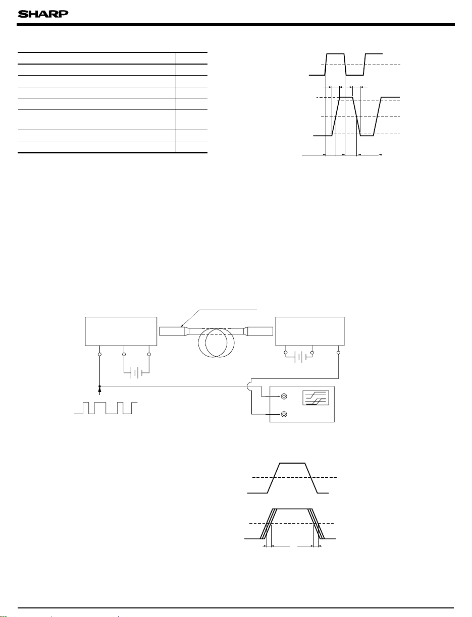
GP1F361R/GP1F361T
Test item
Test item Symbol
Low→High pulse delay time
High→Low pulse delay time
Rise time
Fall time
Pulse width distortion
∆tw = t
PHL-tPLH
High level output voltage V
Low level output voltage V
(1)
V
Notes
=3.0 ±0.05V (State of operating
CC
(2)
The fiber coupling light output set at - 14.5dBm/ - 24.0dBm.
(3)
The probe for the oscilloscope must be more than 1MΩ and less than 10pF.
(4)
The output (H/L level) of GP1F361R are not fixed constantly
when it receivers the disturbing light (including DC light, no input light) less than 0.1Mbps.
Fig. 6 Measuring Method of Jitter
Standard
transmitter
Vin Vcc GND
5V
t
PLH
t
PHL
t
r
t
f
∆tw
OH
OL
)
fiber optic cable
Standard
Transmitter
Input signal
(
)
CH1
V
OH
GP1F361R
Output signal
(
)
CH2
V
OL
t
PLH
GP1F361R
Unit to be measured
GND Vout
Vcc
Vcc
trt
50%
f
90%
50%
10%
t
PHL
Input
Input signal 3Mbps biphase PRBS signal
Input signal
GP1F361R
output
CH1
CH2
Oscilloscope
∆∆
tjr tjf
Tectronix 7834
or 7934 type
Trigger; CH1
Storage mode
Sweep ; AUTO/NORM
50%
50%
Test item
Test item
Low→High jitter
(1)
Notes
The fiber coupling light output set at - 14.5dBm/ - 24.0dBm.
(2)
The waveform write time shall be 3 seconds. But do not allow the waveform to be distorted
by increasing the brightness too much.
(3)
=3.0 ±0.05V (State of operating
V
CC
(4)
The probe for the oscilloscope must be more than 1MΩ and less than 10pF.
Symbol Test condition
∆tjr
∆tjfHigh→Low jitter
GP1F361T/GP1F361R
Set the trigger on the rise of input signal
to measure the jitter of the rise of output
Set the trigger on the fall of input signal
to measure the jitter of the fall of output
)
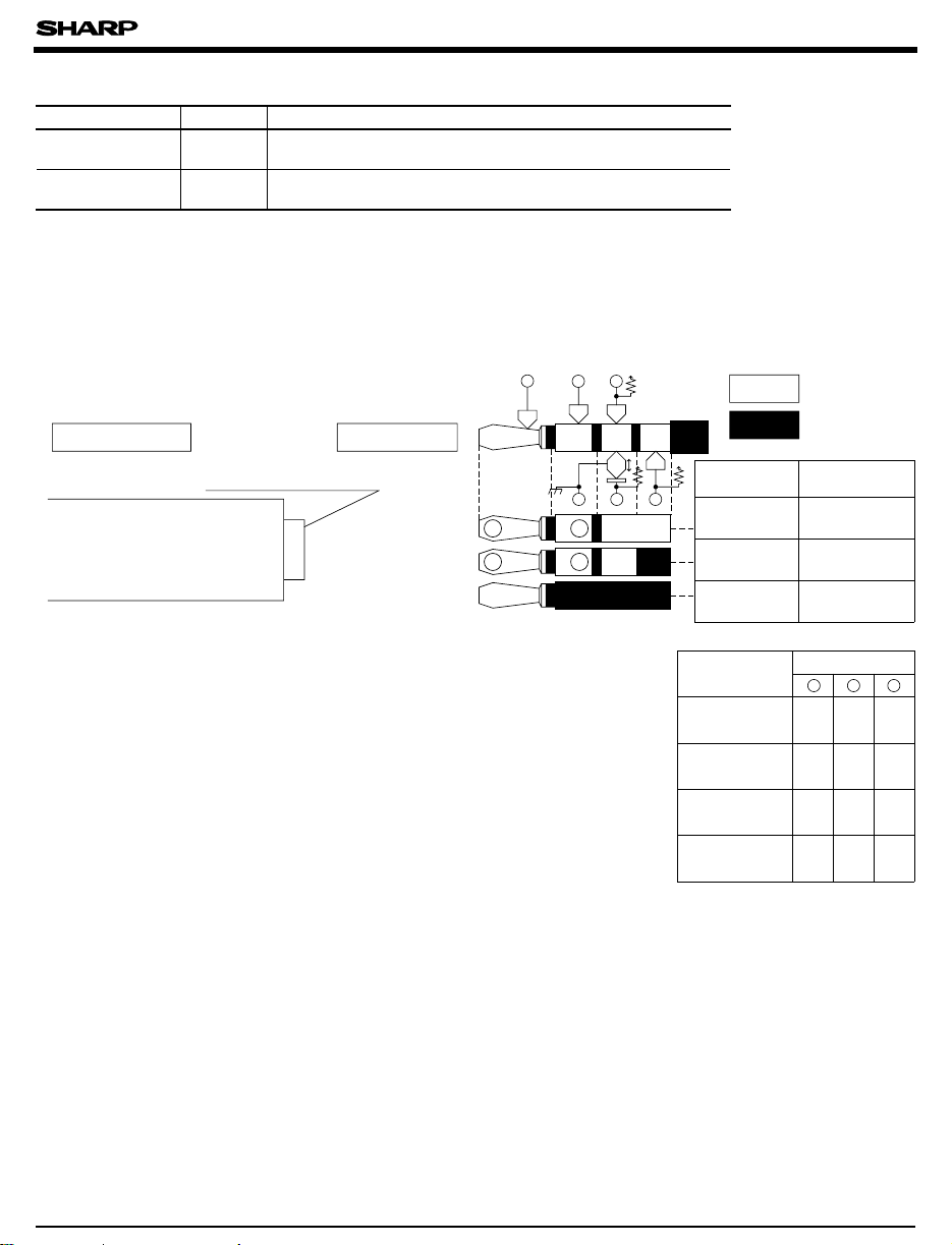
■ Optical Mini-Jack Connection Example
Jack side Plug side
Input or output terminal
Compatible with:
Analog electric signal
Digital electric signal
Digital optical signal
GP1F361R/GP1F361T
●
Please refer to the chapter “ Precautions for Use.”
}
Analog electric signal
Digital electric signal
Digital optical signal
L
+
2
3
5
64
R-GND
GND
: Metal part
: Resin part
1
Input side Output side
LINE IN
MIC HEAD PHONE
Digital input
(
coaxial
Optical Optical
digital input
Kinds of plug
Analog
electricity
Digital
electricity
Digital optics L H H
No plug H H H
)
LINE OUT
Digital output
(
digital output
)
coaxial
Output
451
LLL
LLH
 Loading...