

Page 1
– 1 –
CD-DD4500
No. S7144CDDD4500
CONTENTS
Page
IMPORTANT SERVICE NOTES (FOR U.S.A. ONLY)....................................................................................................... 2
SPECIFICATIONS ............................................................................................................................................................. 2
NAMES OF PARTS ........................................................................................................................................................... 3
OPERATION MANUAL ...................................................................................................................................................... 6
DISASSEMBLY................................................................................................................................................................ 12
REMOVING AND REINSTALLING THE MAIN PARTS................................................................................................... 15
ADJUSTMENT ................................................................................................................................................................. 17
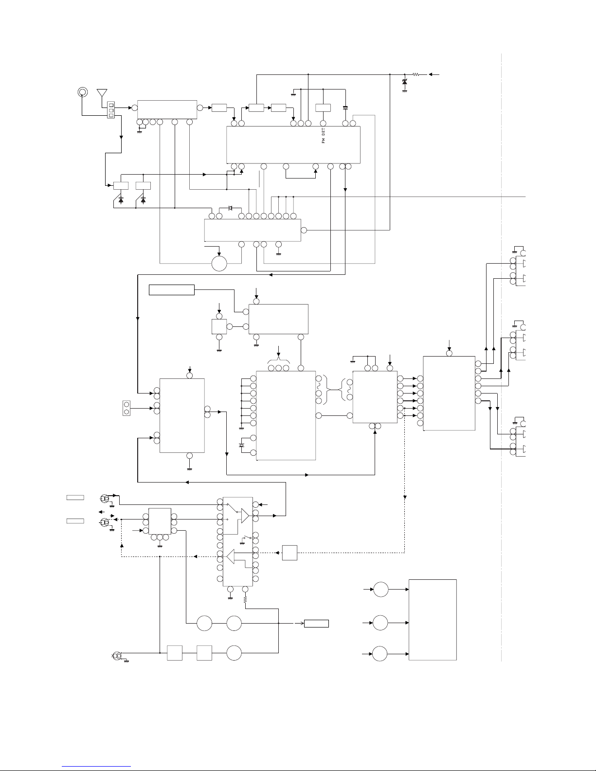
BLOCK DIAGRAM ........................................................................................................................................................... 21
SCHEMATIC DIAGRAM / WIRING SIDE OF P.W.BOARD..............................................................................................24
VOLTAGE ........................................................................................................................................................................ 48
NOTES ON SCHEMATIC DIAGRAM .............................................................................................................................. 49
TYPES OF TRANSISTOR AND LED................................................................................................................................49
WAVEFORMS OF CD CIRCUIT...................................................................................................................................... 50
TROUBLESHOOTING ..................................................................................................................................................... 51
FUNCTION TABLE OF IC................................................................................................................................................ 55
FL DISPLAY......................................................................................................................................................................68
REPLACEMENT PARTS LIST/EXPLODED VIEW
PACKING OF THE SET (FOR U.S.A. ONLY)
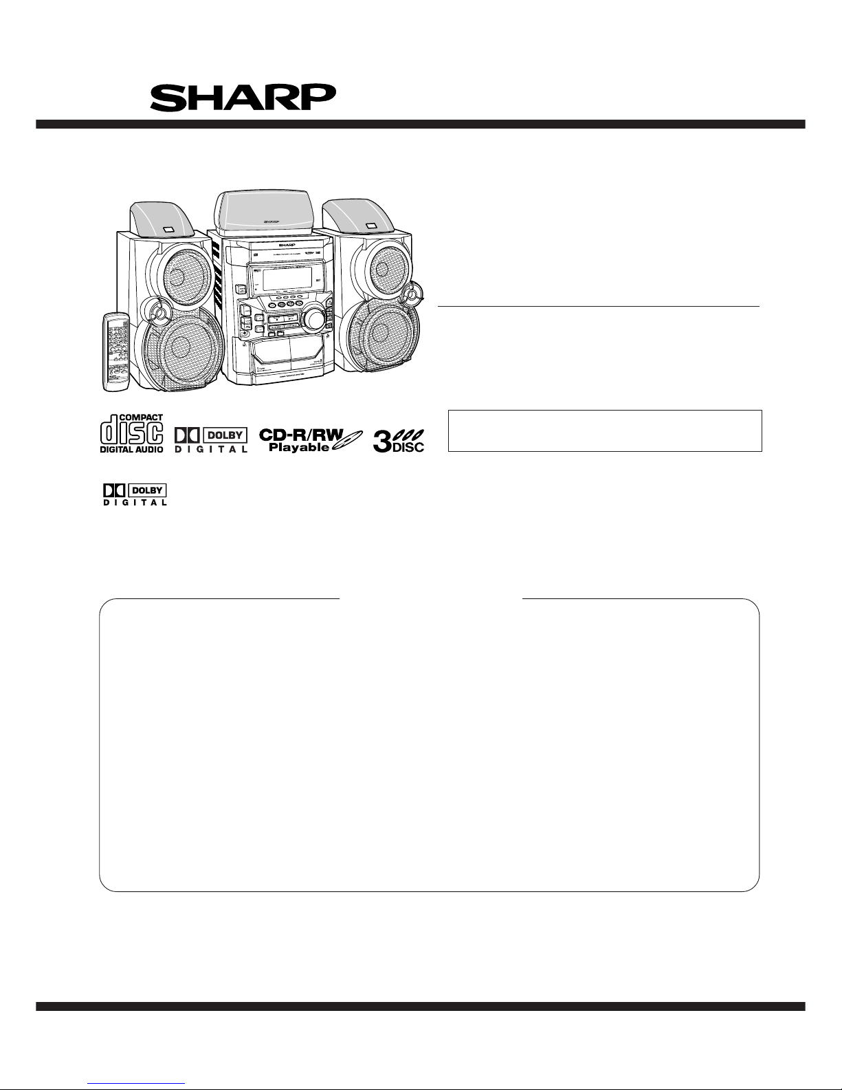
MINI COMPONENT SYSTEM
MODEL CD-DD4500
• In the interests of user-safety the set should be restored to its
original condition and only parts identical to those specified be
used.
SERVICE MANUAL
This document has been published to be used
for after sales service only.
The contents are subject to change without notice.
SHARP CORPORATION
CD-DD4500 Mini Component System consisting of
CD-DD4500 (main unit), CP-DD4500 (Front), center
(GBOXS0064AWM1), surround (R) (GBOXS2008AWM1) and
surround (L) (GBOXS4008AWM1) speaker system.
Manufactured under license from Dolby Laboratories.
"Dolby", "Pro Logic" and the double-D symbol are trademarks of Dolby Laboratories.
Confidential unpublis hed wor ks. © 1992-1997 Dolby Laboratories. All rights reserved.
Page 2
CD-DD4500
– 2 –
CD player
Type 3-disc multi-play compact disc player
Signal readout Non-contact, 3-beam semiconductor laser pickup
D/A converter 1-bit D/A converter
Frequency response 20 - 20,000 Hz
Dynamic range 100 dB (1 kHz)
Tuner
Frequency range FM: 87.5-108 MHz
AM: 530-1,720 kHz
Cassette deck
Frequency response 50 -14,000 Hz (Normal tape)
Signal/noise ratio 55 dB (TAPE 1, playback)
50 dB (TAPE 2, recording/playback)
Wow and flutter 0.25 % (WRMS)
General
Power source AC 120 V, 60 Hz
Power consumption 230 W
Dimensions Width: 10-11/16" (270 mm)
Height: 13" (330 mm)
Depth: 14-11/16" (372 mm)
Weight 19.4 lbs (8.8 kg)
Amplifier
Output power Front speakers (Main) : 30 W minimum RMS per chan-
nel into 8 ohms.
Front speakers (Subwoofer) : 40 W per channel : 6 ohms
(100 Hz, 10 % T.H.D.)
Center speaker : 30W : 6 ohms
(1 kHz, 10 % T.H.D.)
Surround speakers : 20W per channel : 8 ohms
(1 kHz, 10 % T.H.D.)
Output terminals Front speakers (Main) : 8 ohms
Front speakers (Subwoofer) : 6 ohms
Center speaker : 6 ohms
Surround speakers : 8 ohms
Subwoofer(Pre-out) : 10 kohms
Headphones : 16-50 ohms (recommended; 32 ohms)
Input terminals DVD (Digital) : Optical
VCR/Auxiliary : 500 mV/47 kohms
Type 3 - way, 5-1/8" (130 mm) subwoofer, 4" (100 mm)
woofer and 2" (50 mm) tweeter
Maximum input power Subwoofer: 80 W
Main: 60 W
Impedance Subwoofer: 6 ohms/ Main: 8 ohms
Dimensions Width: 8- 5/8" (220 mm)
Height: 13" (330 mm)
Depth: 9- 5/8" (245 mm)
Weight 9.0 lbs. (4.1 kg)/each
Type Full range, 4" (100 mm)
Maximum input power 60 W
Impedance 6 ohms
Dimensions Width: 10- 1/4" (260 mm)
Height: 5- 5/8" (142 mm)
Depth: 6- 11/16" (170 mm)
Weight 2.2 lbs. (1.0 kg)/each
Type Full range, 4" (100 mm)
Maximum input power 40 W
Impedance 8 ohms
Dimensions Width: 7- 7/8" (200 mm)
Height: 6- 3/4" (172 mm)
Depth: 3- 3/4" (95 mm)
Weight 1.3 lbs. (0.6 kg)/each
FOR A COMPLETE DESCRIPTION OF THE OPERATION OF THIS UNIT, PLEASE REFER
TO THE OPERATION MANUAL.
Specifications for this model are subject to change without
prior notice.
SPECIFICATIONS
CD-DD4500
CP-DD4500
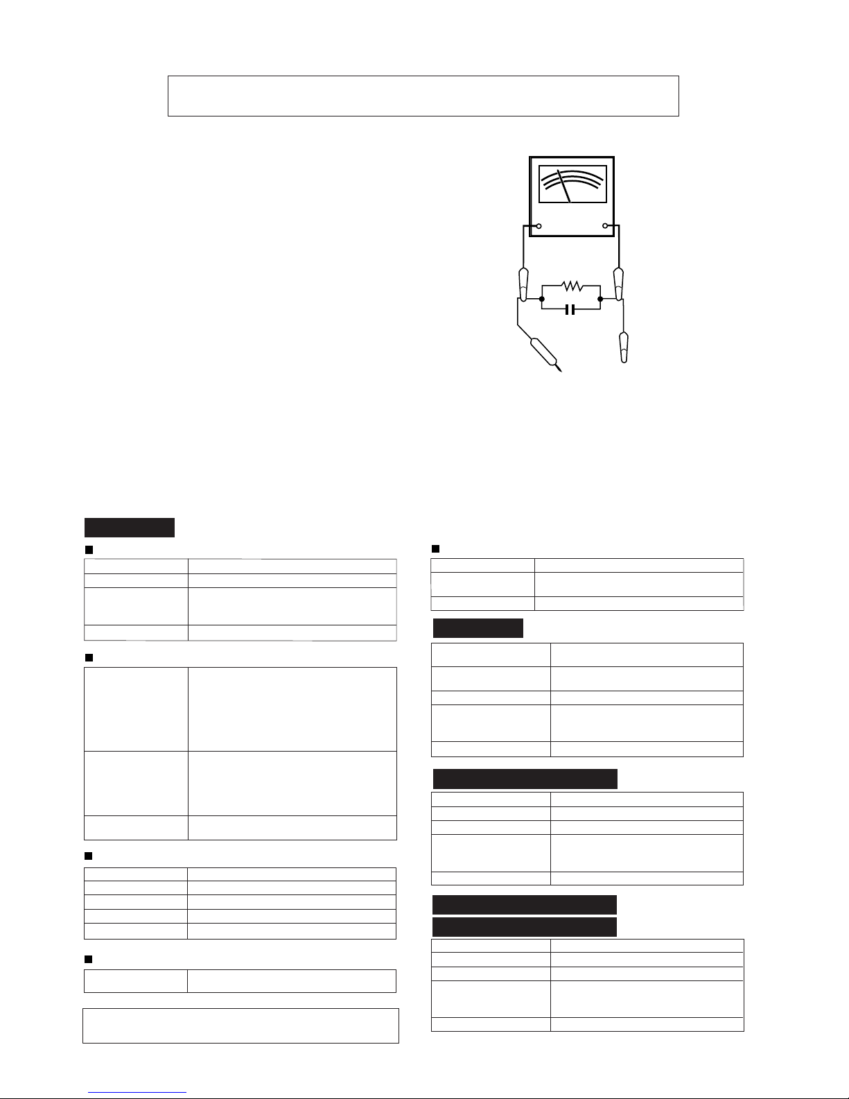
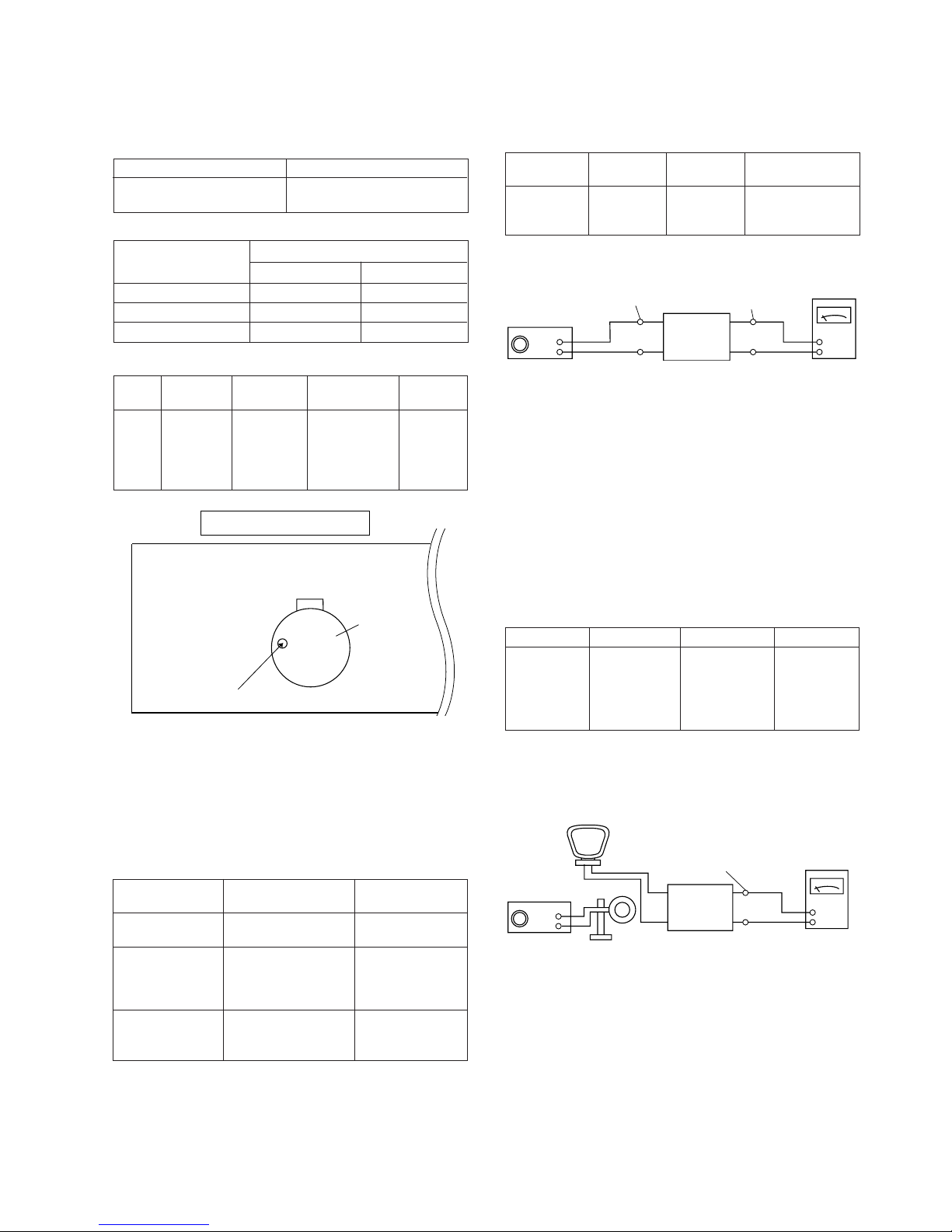
IMPORTANT SERVICE NOTES (FOR U.S.A. ONLY)
BEFORE RETURNING THE AUDIO PRODUCT
(Fire & Shock Hazard)
Before returning the audio product to the user, perform the
following safety checks.
1. Inspect all lead dress to make certain that leads are not
pinched or that hardware is not lodged between the chassis
and other metal parts in the audio product.
2. Inspect all protective devices such as insulating materials,
cabinet, terminal board, adjustment and compartment covers
or shields, mechanical insulators etc.
3. To be sure that no shock hazard exists, check for leakage
current in the following manner.
* Plug the AC line cord directly into a 120 volt AC outlet.
* Using two clip leads, connect a 1.5k ohm, 10 watt resistor
paralleled by a 0.15µF capacitor in series with all exposed
metal cabinet parts and a known earth ground, such as
conduit or electrical ground connected to earth ground.
* Use a VTVM or VOM with 1000 ohm per volt, or higher,
sensitivity to measure the AC voltage drop across the
resistor (See diagram).
* Connect the resistor connection to all exposed metal parts
having a return path to the chassis (antenna, metal cabinet,
screw heads, knobs and control shafts, escutcheon, etc.)
and measure the AC voltage drop across the resistor.
All check must be repeated with the AC line cord plug connection
reversed.
Any reading of 0.3 volt RMS (this corresponds to 0.2 milliamp.
AC.) or more is excessive and indicates a potential shock
hazard which must be corrected before returning the audio
product to the owner.
TO EXPOSED
METAL PARTS
CONNECT TO
KNOWN EARTH
GROUND
TEST PROBE
0.15 µ F
1.5k ohms
10W
VTVM
AC SCALE
GBOXS0064AWM1
GBOXS2008AWM1
GBOXS4008AWM1
Page 3
– 3 –
CD-DD4500
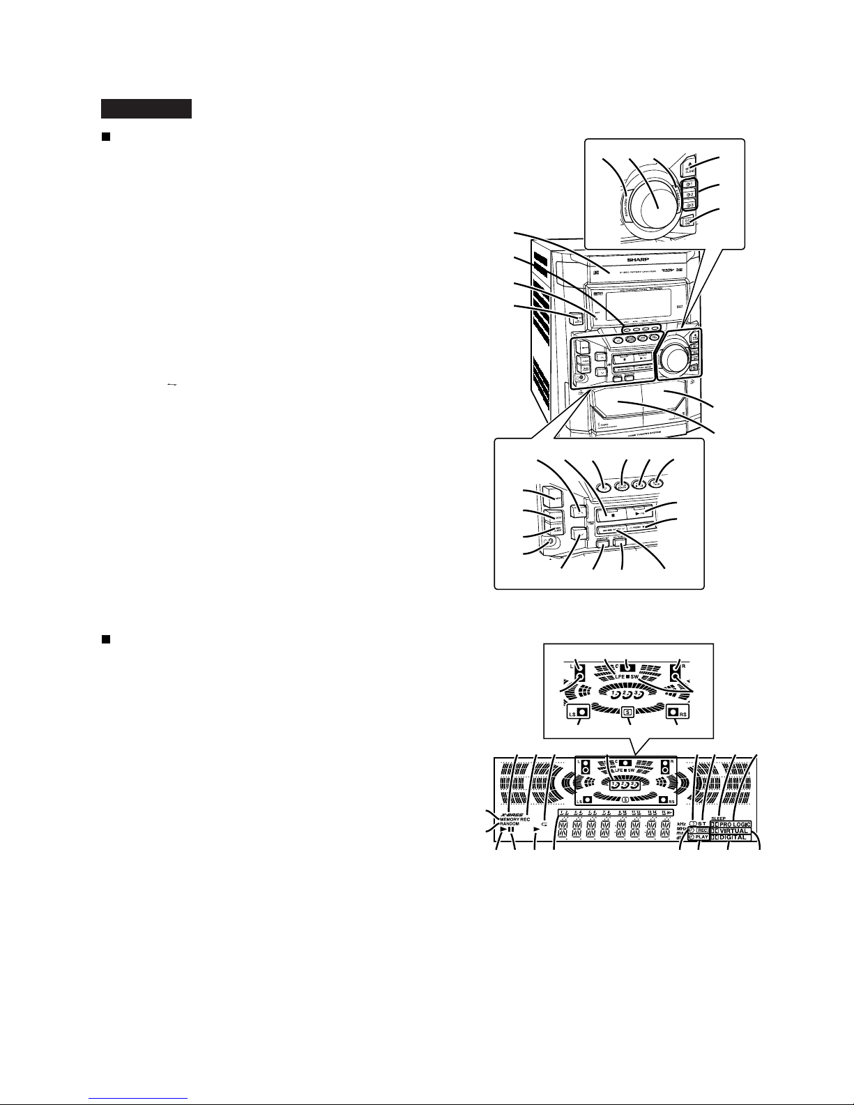
NAMES OF PARTS
CD-DD4500
Front panel
1. Disc Tray
2. Surround Effect Buttons
3. Timer Set Indicator
4. Power On/Stand-by Button
5. Tape 2 Cassette Compartment
6. Tape 1 Cassette Compartment
7. Equalizer Mode Select Button
8. Volume Control
9. Extra Bass/Demo Mode Button
10. Disc Tray Open/Close Button
11. Disc Number Select Buttons
12. Disc Skip Button
13. Tuning and Time Up Button
14. CD or Tape Stop Button (with Indicator)
15. CD Button
16. Tuner (Band) Button
17. Tape (1 2) Button
18. DVD/VCR Button
19. Dimmer Button
20. Clock Button
21. Timer/Sleep Button
22. Headphone Jack
23. CD Play or Repeat, Tape Play Button
(with Indicator)
24. CD Fast Forward, Tape 2 Fast Forward
or Tuner Preset Up Button
25. Tuning and Time Down Button
26. Memory/Set Button
27. Tape 2 Record Pause Button
28. CD Fast Reverse, Tape 2 Rewind
or Tuner Preset Down Button
5
6
7
1
2
3
4
9
10
11
12
19
23
181716151413
25 26 27 28
24
20
21
22
8
Display
1. Left Front Speaker Indicator
2. Low Frequency Effect Indicator
3. Center Speaker Indicator
4. Right Front Speaker Indicator
5. Subwoofer Indicator
6. Left Surround Speaker Indicator
7. Surround Indicator
8. Right Surround Speaker Indicator
9. Extra Bass Indicator
10. Tape 2 Record Indicator
11. CD Repeat Indicator
12. Disc Number Indicators
13. FM Stereo Receiving Indicator
14. FM Stereo Mode Indicator
15. Sleep Indicator
16. Dolby Pro Logic Indicator
17. Memory Indicator
18. CD Random Play Indicator
19. CD Play Indicator
20. CD Pause Indicator
21. Tape Play Indicator
22. CD Music Schedule Indicators
23. Timer Recording Indicator
24. Timer Play Indicator
25. Dolby Digital Indicator
26. Dolby Virtual Indicator
26
9
17
18
19
20
22 2324 25
1011 13 14 15 16
21
1 2
68
5
12
4
7
5
3
Page 4
CD-DD4500
– 4 –
CD-DD4500
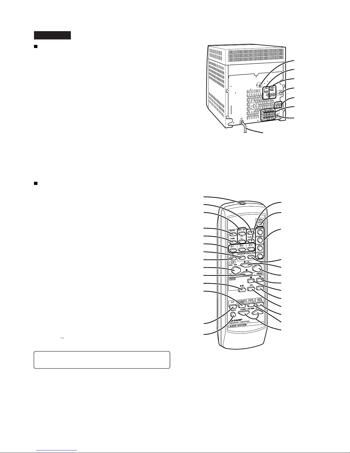
Rear panel
1. DVD Digital Input Jack
2. Center Speaker Jacks
3. Surround Speaker Jacks
4. FM/AM Loop Antenna Jack
5. Video/Auxiliary (Audio Signal) Input Jacks
6. Speaker Terminals
7. Subwoofer Pre Output Jack
8. AC Power Cord
1
8
2
3
4
5
6
7
Remote control
1. Remote Control Transmitter
2. CD Memory Button
3. Set Up Menu Select Buttons
4. Menu Button
5. Item Button
6. Disc Number Select Buttons
7. CD Random Button
8. CD Pause Button
9. CD Fast Reverse/Preset Down Button
10. CD Stop Button
11. Tape 2 Record Pause Button
12. Tuner (Band) Button
13. CD Button
14. Extra Bass Button
15. CD Clear Button
16. Power Button
17. Surround Effect Buttons
18. Equalizer Mode Select Button
19. CD Play or Repeat Button
20. CD Fast Forward/Preset Up Button
21. Tape 1/Tape 2 Play Button
22. Tape 1/Tape 2 Stop Button
23. Tape 2 Fast Forward Button
24. Tape 2 Rewind Button
25. DVD/VCR Button
26. Tape (1 2) Button
27. Volume Up or Down Buttons
11
2
15
16
17
20
3
5
6
7
8
9
13
14
12
11
10
4
21
27
26
25
24
23
22
18
19
✱
✱
✱
✱
✱
✱
Buttons with “✱” mark in the illustration can be operated with the remote control
only.
Other buttons can be operated on the main unit and the remote control.
Page 5
– 5 –
CD-DD4500
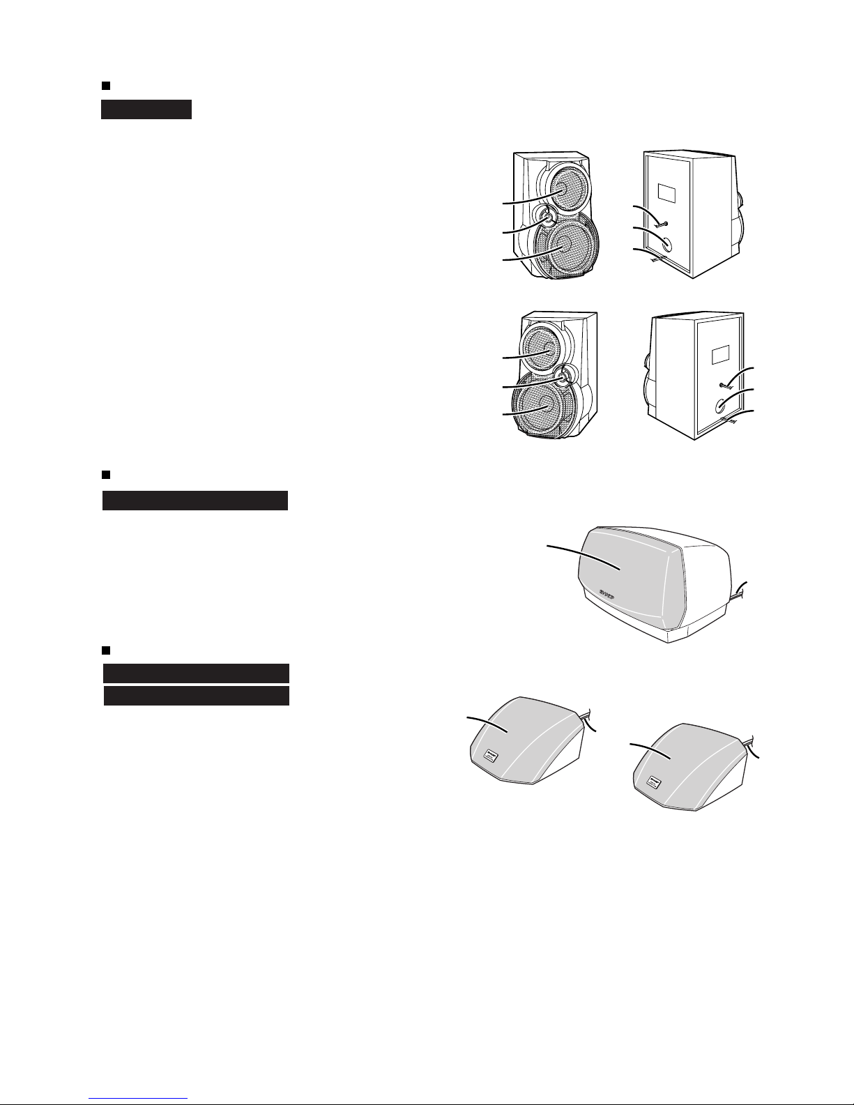
CP-DD4500
Center Speaker
Front Speaker
Surround Speaker
1. Woofer
2. Tweeter
3. Subwoofer
4. Speaker Wire for SUBWOOFER Terminals
5. Bass Reflex Duct
6. Speaker Wire for MAIN Terminals
Front speaker
(left)
Front speaker
(right)
2
1
3
2
1
3
4
5
6
4
5
6
2
1
2
1
1. Full-Range Speaker
2. Speaker Wire
1. Full-Range Speaker
2. Speaker Wire
2
1
GBOXS0064AWM1
GBOXS2008AWM1
GBOXS4008AWM1
Page 6
CD-DD4500
– 6 –
OPERATION MANUAL
To confirm the time display:
Press the CLOCK button.
The time display will appear for about 5 seconds.
Note:
The “CLOCK” or time will flash at the push of the CLOCK button when the AC power
supply is restored after a power failure or after unplugging the unit.
Readjust the clock as follows.
To readjust the clock:
Perform “Setting the Clock” from the beginning.
If the time display is flashing, step 3 (for selecting the 12-hour or 24-hour display) will
be skipped.
To change the 12-hour or 24-hour display:
1. Clear all the programmed contents.
[Refer to “Clearing all the memory (reset)”.]
2. Perform “Setting the Clock” from the beginning.
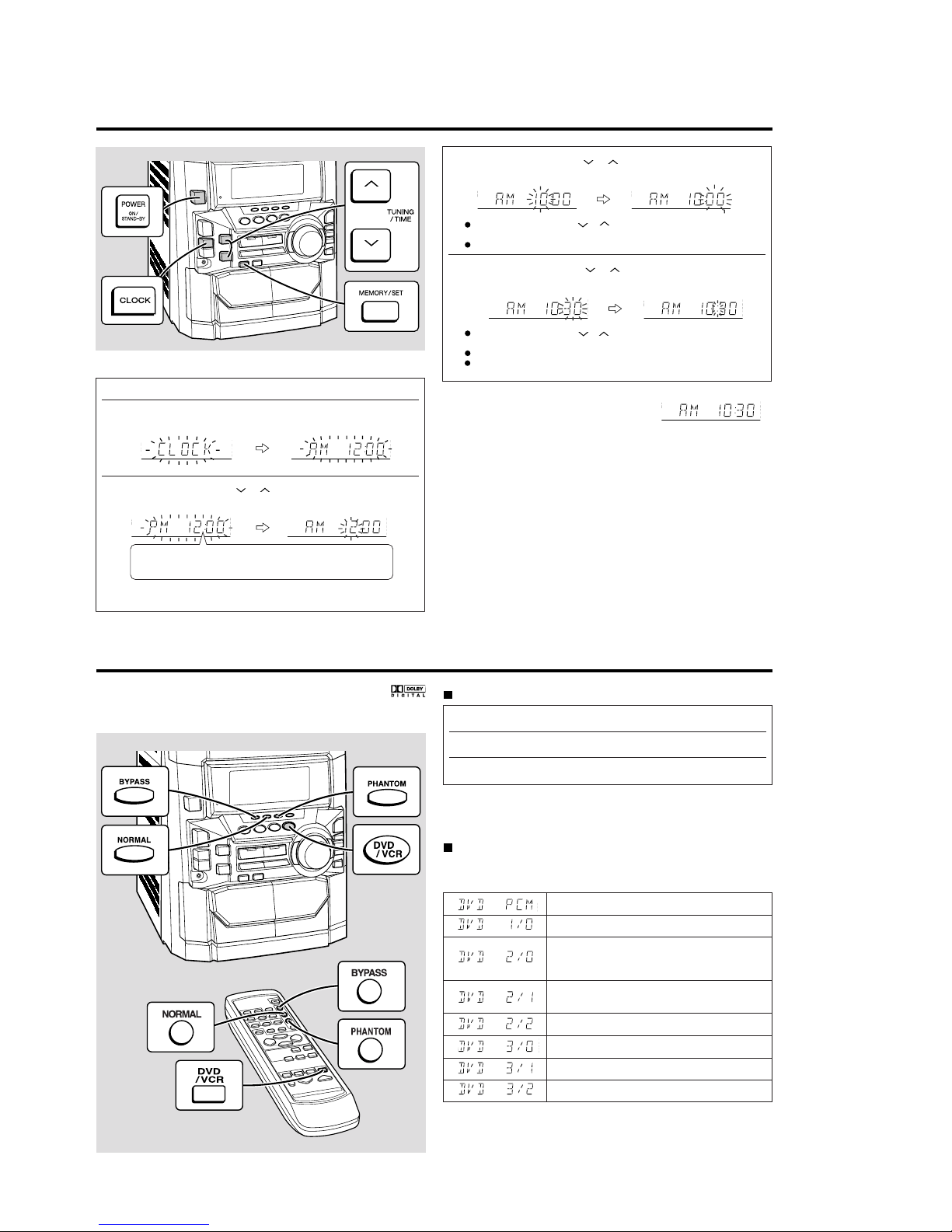
Setting the Clock
In this example, the clock is set for the 12-hour (AM 12:00) display.
1
Press the POWER button to turn the power on.
2
Press the CLOCK button and within 5 seconds, press the
MEMORY/SET button.
3
Press the TUNING/TIME ( or ) button to select the 12-hour or
24-hour display and then press the MEMORY/SET button.
4
Press the TUNING/TIME ( or ) button to adjust the hour and
then press the MEMORY/SET button.
Press the
TUNING/TIME ( or )
button once to advance the time by 1
hour. Hold it down to advance continuously.
When the 12-hour display is selected, “AM” will change automatically to “PM”.
5
Press the TUNING/TIME ( or ) button to adjust the minutes
and then press the MEMORY/SET button.
Press the
TUNING/TIME ( or )
button once to advance the time by 1
minute. Hold it down to change the time in 5-minute intervals.
The hour will not advance even if minutes advance from “59” to “00”.
The clock begins counting from “0” seconds. (Seconds are not displayed.)
The time display will disappear after a few seconds.
Note that this can only be set when the unit is first installed or it has been reset.
When you connect this unit to a DVD player which is playing a disc with the
trademark, you can enjoy realistic, powerful sound by playing back the recorded signal
through 5 speakers with the sound coming from the front left, front right, center, surround left and surround right speakers.
Dolby Digital
To listen to a disc using the Dolby Digital mode
1
Connect a DVD player.
2
Press the DVD/VCR button to select “DVD”.
3
Start the DVD player.
Note:
When in the Dolby Digital surround mode, the equalizer will be set to FLAT.
Type of Dolby digital signal
There are different types of Dolby digital signals. The type of Dolby digital signal being
input into this unit can be checked in the display.
If a low frequency sound effect (Low Frequency Effect) contains a Dolby digital signal,
“LFE” will light in the display.
When this “LFE” is lit, low frequency signals will be output from the subwoofer.
Normal PCM playback
Center only (monaural)
Front (L, R)
(When the surround mode is set to Normal or Phantom,
sound will also be heard from the surround speakers.)
Front (L, R) + surround
(monaural)
Front (L, R) + surround (L, R)
Front (L, R) + center
Front (L, R) + center + surround (monaural)
Front (L, R) + center + surround (L, R)
“AM 12:00”→ The 12-hour display will appear. (AM 12:00 - PM 11:59)
“AM 0:00” → The 12-hour display will appear. (AM 0:00 - PM 11:59)
“0:00” → The 24-hour display will appear. (0:00 - 23:59)
Page 7
– 7 –
CD-DD4500
Troubleshooting Chart
Many potential “problems” can be resolved by the owner without calling a service technician. If something is wrong with this product, check the following before calling your
authorized SHARP dealer or service center.
Tuner
Symptom
Radio makes unusual noise consecutively.
Possible cause
Is the unit placed near the TV or computer?
Is the FM/AM loop antenna placed properly?
Move the AC power cord away from the
antenna if located near.
General
Symptom
The clock is not on time.
When a button is pressed, the unit
does not respond.
No sound is heard.
The balance between the left and
right channels is bad.
Hum or excessive noise.
No sound is heard, or the sound
is too low, from the center or surround speakers.
The TIMER indicator is flashing.
CD player
Symptom
Playback does not start.
Playback stops in the middle or is
not performed properly.
Playback sounds are skipped, or
stopped in the middle of a track.
Possible cause
Is the disc loaded upside down?
Does the disc satisfy the standards?
Is the disc distorted or scratched?
Is the unit located near excessive vibrations?
Is the disc very dirty?
Has condensation formed inside the
unit?
Possible cause
Did a power failure occur?
Reset the clock.
Set this unit to the power stand-by mode
and then turn it back on.
If the unit still malfunctions, reset it.
Is the volume level set to “0”?
Are the headphones connected?
Are the speaker wires disconnected?
Are the front and surround speakers
connected to the correct left and right
channels?
If an external unit is connected, are the
left and right channels connected properly?
Is the speaker cord plugged in correctly?
Does the speaker cord run past other
electronic equipment?
Are the plugs or terminals dirty?
Is the “SP SIZE” item set to “NO” in the
“SET UP” operation?
Is the volume too low?
Is the speaker wire shorted?
Was the unit used at high volume for
many hours?
Cassette deck
Symptom
Cannot record.
Cannot record tracks with proper
sound quality.
Cannot erase completely.
Sound skipping.
Cannot hear treble.
Sound fluctuation.
Cannot remove the tape.
Possible cause
Is the erase-protection tab removed?
Is it a normal tape?
(You cannot record on a metal or CrO
2
tape.)
Is there any slack?
Is the tape stretched?
Are the capstans, pinch rollers, or heads
dirty?
If a power failure occurs during playback,
the heads remain engaged with the tape.
Do not open the compartment forcibly.
Wait until electricity resumes.
Remote control
Symptom
The remote control does not operate.
Possible cause
Is the AC power cord of the unit plugged
in?
Is the battery polarity respected?
Are the batteries dead?
Is the distance or angle incorrect?
Does the remote control sensor receive
strong light?
Condensation
Sudden temperature changes, storage or operation in an extremely humid environment may cause condensation inside the cabinet (CD pickup, tape heads,
etc.) or on the transmitter on the remote control.
Condensation can cause the unit to malfunction.
If this happens, leave the power on with no disc (or cassette) in the unit until
normal playback is possible (about 1 hour). Wipe off any condensation on the
transmitter with a soft cloth before operating the unit.
Connecting DVD player
Symptom
Although a DVD player is connected, no sound is heard.
Possible cause
Is the power to the DVD player connected properly?
Is a digital signal being output from the
DVD player?
Is “DVD NO” being displayed?
Does the type of DVD digital signal appear in the display?
Since “DVD---” is not output from the
Dolby digital source, it cannot be
decorded.
Is a Dolby digital 2/0 (monaural) signal
being played with the surround mode set
to NORMAL and without a center
speaker connected?
If trouble occurs
When this product is subjected to strong external interference (mechanical shock, excessive static electricity, abnormal supply voltage due to lightning, etc.) or if it is operated incorrectly, it may malfunction.
If such a problem occurs, do the following:
1
. Set the unit to the stand-by mode and turn the power on again.
2
. If the unit is not restored in the previous operation, unplug and plug in the
unit, and then turn the power on.
Note:
If neither operation above restores the unit, clear all the memory by resetting it.
Page 8
CD-DD4500
– 8 –
Notes concerning use:
Replace the batteries if the operating distance is reduced or if the operation be-
comes erratic.
Periodically clean the transmitter on the remote control and the sensor on the unit
with a soft cloth.
Exposing the sensor on the unit to strong light may interfere with operation. Change
the lighting or the direction of the unit.
Keep the remote control away from moisture, heat, shock, and vibrations.
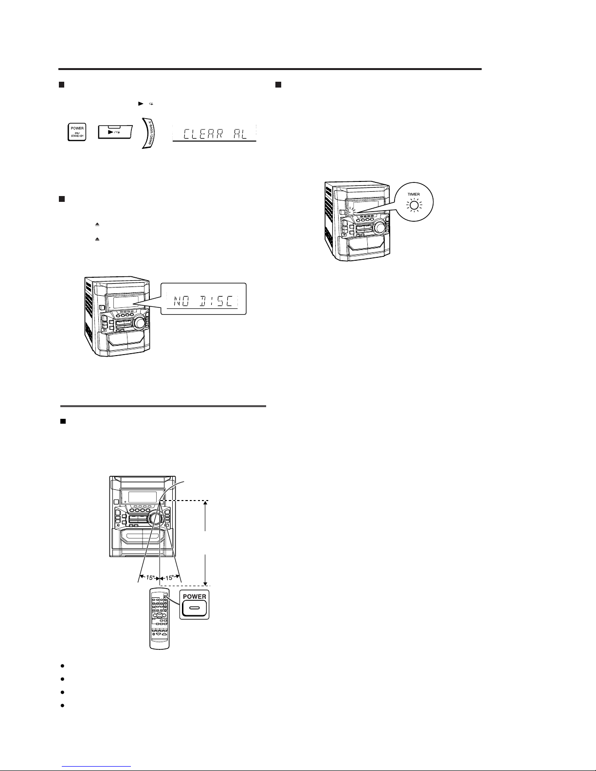
Test of the remote control
Face the remote control directly to the remote sensor on the unit.
The remote control can be used within the range shown below:
Press the POWER button. Does the power turn on? Now, you can enjoy the music.
Remote Control
8" - 20'
(0.2 m - 6 m)
Remote sensor
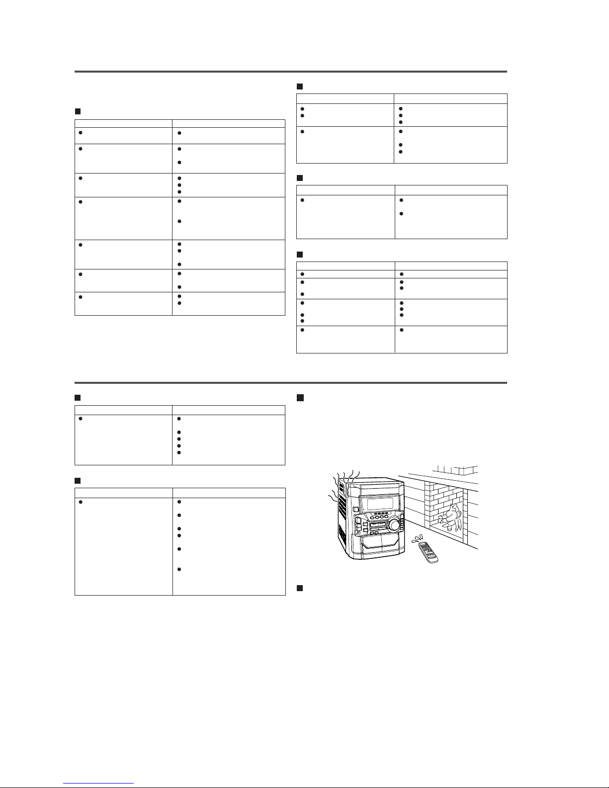
When TIMER indicator is flashing
The unit will be overheated when TIMER indicator is flashing.
Due to a problem in the speaker circuit, the unit will enter the stand-by mode
automatically.
In this case, take the following corrective actions.
1
. Unplug the AC power plug from the AC outlet.
2
. Make sure that the unit vent is not blocked.
3
. Make sure that the speaker wires have been correctly connected to the
speaker terminals.
4
. After checking items 2 and 3 above, wait for 2 or 3 hours before trying to use
the unit.
5
. Reconnect the AC power cord.
Note:
If the TIMER indicator flashes again during use, please unplug the AC power plug,
and contact a SHARP authorized service center.
Troubleshooting Chart
Before transporting the unit
1.
Press the POWER button to turn the power on.
2.
Press the CD button.
3.
Press the OPEN/CLOSE button to open the disc tray.
Remove all CDs inserted the unit.
4.
Press the OPEN/CLOSE button to close the disc tray.
Make sure that “NO DISC” is displayed.
5.
Press the POWER button to enter the stand-by mode, and then unplug the
AC power cord from the AC outlet.
Clearing all the memory (reset)
1
. Press the POWER button to enter the power stand-by mode.
2
. While pressing down the / button and X-BASS/DEMO button, press
the POWER button until “CLEAR AL” appears.
Caution:
This operation will erase all data stored in memory including clock, timer settings,
tuner preset, CD program, and other set-up details.
Page 9
– 9 –
CD-DD4500
Accessories
Accesorios
1
FM/AM loop antenna × 1
Antena de cuadro de FM/AM
×
1
Remote control × 1
Controlador remoto
×
1
1
3
2
Battery Installation of the Remote Control
Instalación de las pilas del controlador remoto
Use 2 “AA” size batteries (UM/SUM-3, R6, HP-7 or similar). Batteries are not included.
Use dos pilas del tamaño “AA” (UM/SUM-3, R6, HP-7 o equivalentes). Las pilas no están incluidas.
Remove the
Insert the batteries
Replace the cover.
battery cover.
as shown.
Extraiga la cubierta Inserte las pilas Vuelva a colocar la
de las pilas. como se muestra. cubierta.
2
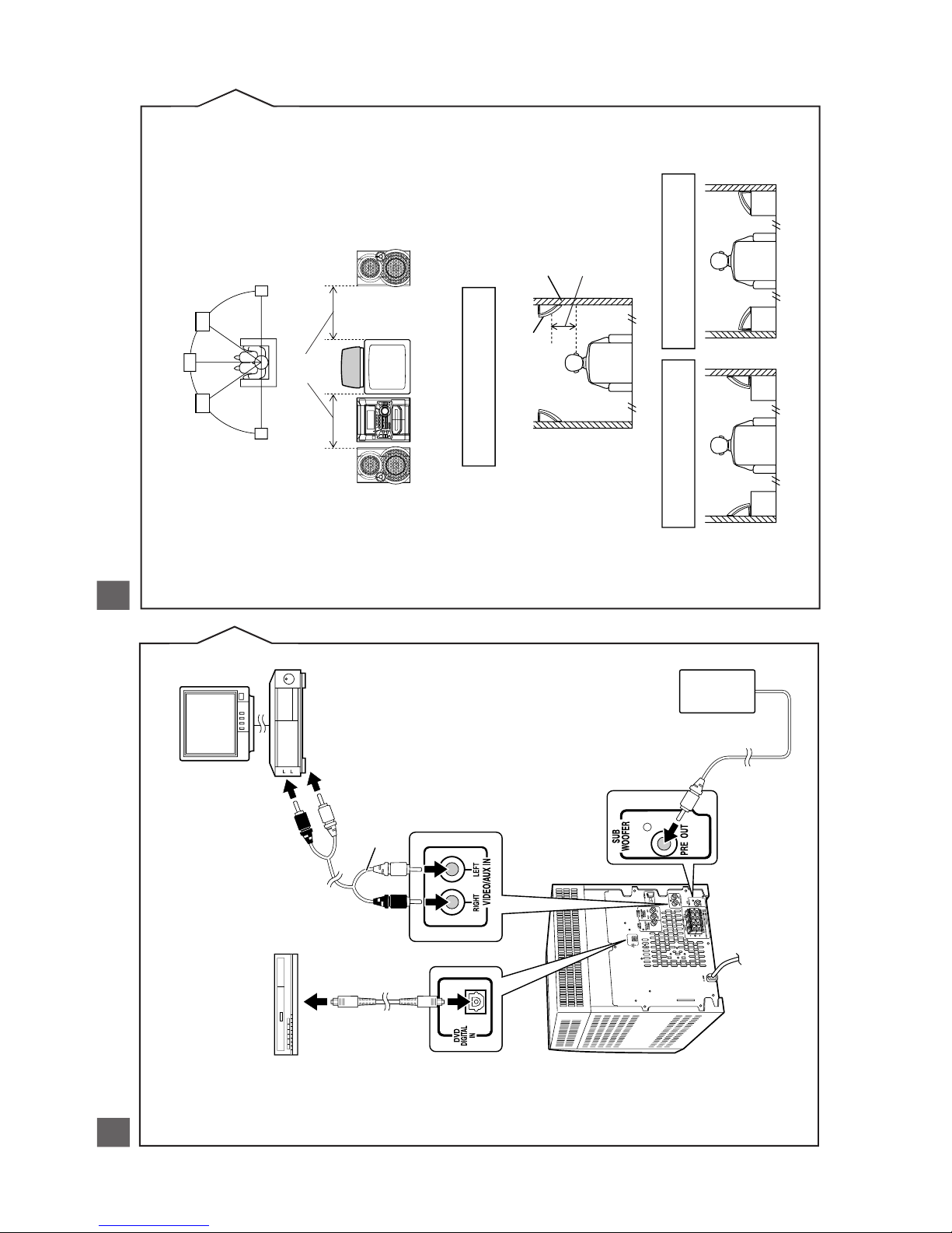
System Connections
Conexiones del sistema
3
AC outlet
(AC 120 V, 60 Hz)
A un tomacorriente de
CA (120 V de CA, 60 Hz)
Front speaker (Right)
Altavoz delantero (Derecho)
Front speaker (Left)
Altavoz delantero
(Izquierdo)
FM antenna
Antena de FM
AM loop antenna
Antena de cuadro de AM
Blue
Azul
Red
Rojo
Black
Negro
Black
Negro
Blue
Azul
Red
Rojo
Black
Negro
Black
Negro
Surround speaker (Right)
Altavoz de sonido perimétrico
(Derecho)
Surround
speaker
(Left)
Altavoz de
sonido
perimétrico
(Izquierdo)
Center speaker
Altavoz central
Right
Derecho
Left
Izquierdo
Page 10
CD-DD4500
– 10 –
External unit Connections
Conexiones de unidades externas
RCA cord
(not supplied)
Cable RCA
(no suministrado)
To the line output jack
A la toma de salida de línea
VCR
Videograbadora
TV
TV
DVD player
Reproductor DVD
Digital cord
(not supplied)
Cable digital
(no suministrado)
Speaker with a
built-in amplifier
Altavoz con amplificador
incorporado
4
Front left
Delantero izquierdo
Center
Central
Front right
Delantero derecho
Surround left
Sonido perimétrico
izquierdo
Surround right
Sonido perimétrico
derecho
Same distance
Misma distancia
Front left
Delantero izquierdo
Center
Central
Front right
Delantero derecho
Example: When installed on the wall
Ejemplo: Cuando se instalan en la pared
Surround speaker
Altavoz de sonido
perimétrico
Wall
Pared
23-5/8" - 35-7/16"
(60 - 90 cm)
60 - 90 cm
Example: When installed vertically
Ejemplo: Cuando se instalan verticalmente
Example: When installed horizontally
Ejemplo: Cuando se instalan horizontalmente
Placing the speakers
Situación de los altavoces
5
Page 11
– 11 –
CD-DD4500
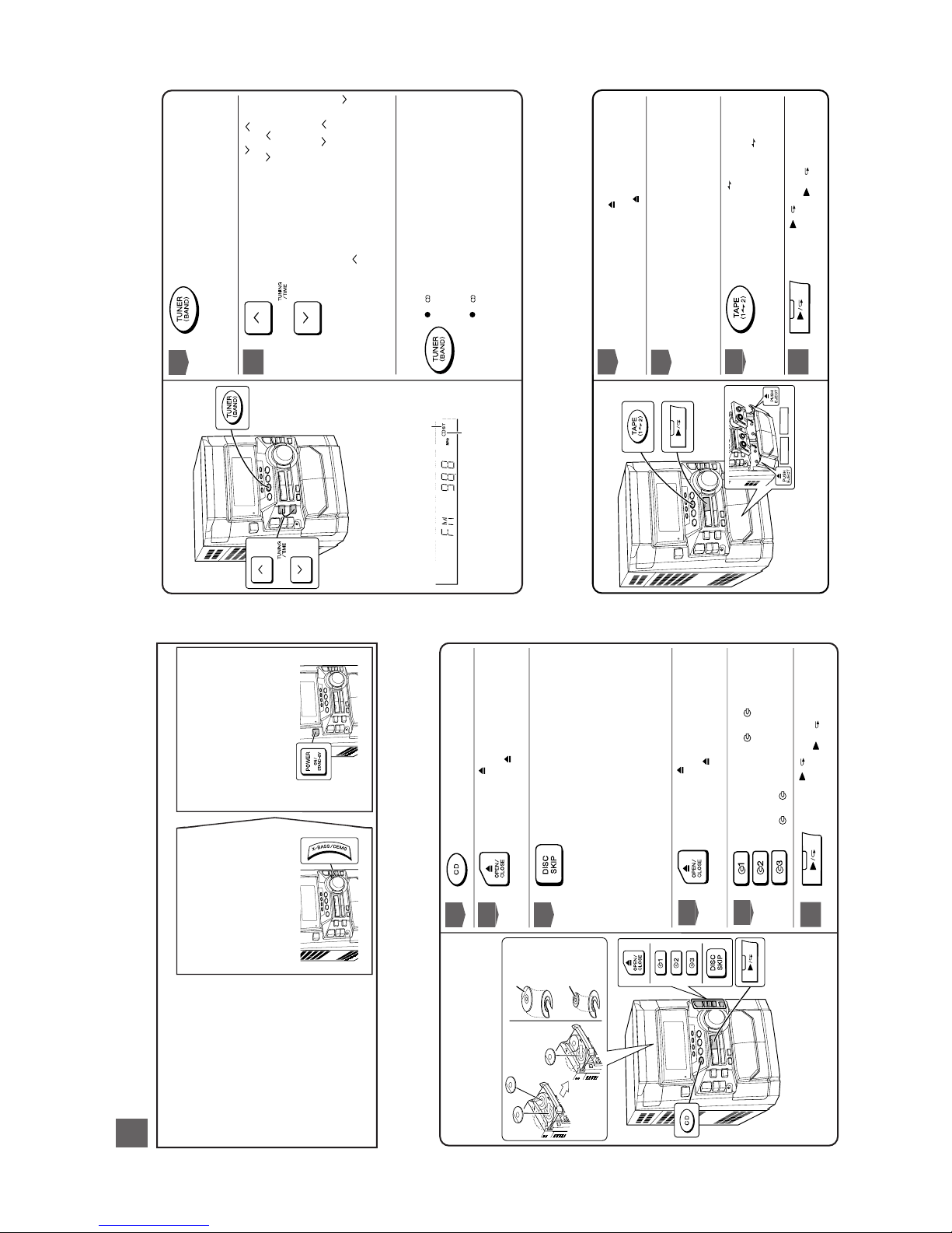
Turning on Your System
Conexión de la alimentación de su sistema
The first time the unit is plugged,
the unit will enter the demonstra-
tion mode. You will see words
scroll.
Cuando se enchufe por primera vez
el aparato, se establecerá en el
modo de demostración. Verá un
desplazamiento de palabras.
5” (12 cm)
12 cm
3” (8 cm)
8 cm
Listening to a CD (CDs)
Audición de un disco CD (discos CD)
1
Press the CD button.
Pulse el botón CD.
2
Press the OPEN/CLOSE button to
open the disc tray.
Pulse el botón OPEN/CLOSE para abrir
la bandeja de discos.
3
Place the CD(s) on the disc tray, label
side up.
When loading a third disc, press the
DISC SKIP button to turn the disc tray,
then place the CD in the open position.
Coloque el disco compacto en la bandeja
de discos, con el lado de la etiqueta hacia
arriba.
Cuando ponga un tercer disco, pulse el
botón DISC SKIP para girar la bandeja de
discos, y coloque el disco compacto en la
posición abierta.
4
Press the OPEN/CLOSE button to
close the disc tray.
Pulse el botón OPEN/CLOSE para cerrar
la bandeja de discos.
5
To select the CD you want to listen to
first, press one of 1 - 3 buttons.
Para seleccionar el disco CD que desee
escuchar primero, pulse uno de los botones
1 - 3.
6
Press the
/
button to start playback.
Pulse el botón
/
para iniciar la
reproducción.
6
Press the
X-BASS/DEMO
button to cancel
the demonstration
mode.
Pulse el botón
X-BASS/DEMO para
cancelar el modo de
demostración.
Press the POWER
button to turn the
power on.
Pulse el botón POWER
para conectar la
alimentación.
12
Listening to a Cassette Tape (TAPE 1 or TAPE 2)
Audición de una cinta de cassette (TAPE 1 o TAPE 2)
Listening to the Radio
Audición de la radio
TAPE 1
TAPE 2
FM stereo mode indicator
Indicador del modo de FM
en estéreo
FM stereo receiving indicator
Indicador de recepción de FM
en estéreo
1
Press the TUNER (BAND) button repeat-
edly to select the desired frequency
band (FM or AM).
Pulse repetidamente el botón TUNER
(BAND) para seleccionar la banda de
frecuencia deseada (FM o AM).
2
Press the TUNING/TIME ( or ) but-
ton to tune in to the desired station.
When the TUNING/TIME ( or ) button
is pressed for more than 0.5 seconds,
scanning will start automatically and the
tuner will stop at the first receivable
broadcast station.
Pulse el botón TUNING/TIME ( o ) para
sintonizar la emisora deseada.
Cuando se pulse el botón
TUNING/TIME (
o ) durante más de 0,5 segundos, la
exploración se iniciará automáticamente y
el sintonizador se parará en la primera
emisora difusora que pueda recibirse.
To receive an FM stereo transmission:
Press the TUNER (BAND) button to display “ST”.
“ ” will appear when an FM broadcast is in ste-
reo.
Para recibir una transmisión de FM en estéreo:
Pulse el botón TUNER (BAND) para visualizar “ST”.
“ ” aparecerá cuando una difusión de FM sea en
estéreo.
1
Open the cassette door by pushing the
area marked “ PUSH EJECT”.
Abra la puerta del cassette pulsando la
parte marcada “ PUSH EJECT”.
2
Load the cassette into the TAPE 1 or
TAPE 2 cassette compartment with the
side to be played facing toward you.
Cargue el cassette en el compartimiento
de cassette de TAPE 1 o de T APE 2 con la
cara a reproducirse encarada hacia usted.
3
Press the TAPE (1 2) button to select
the cassette you want to listen to.
Pulse el botón TAPE (1 2) para
seleccìonar el cassette que desee
escuchar.
4
Press the / button to start playback.
Pulse el botón / para iniciar la
reproducción.
Page 12
CD-DD4500
– 12 –
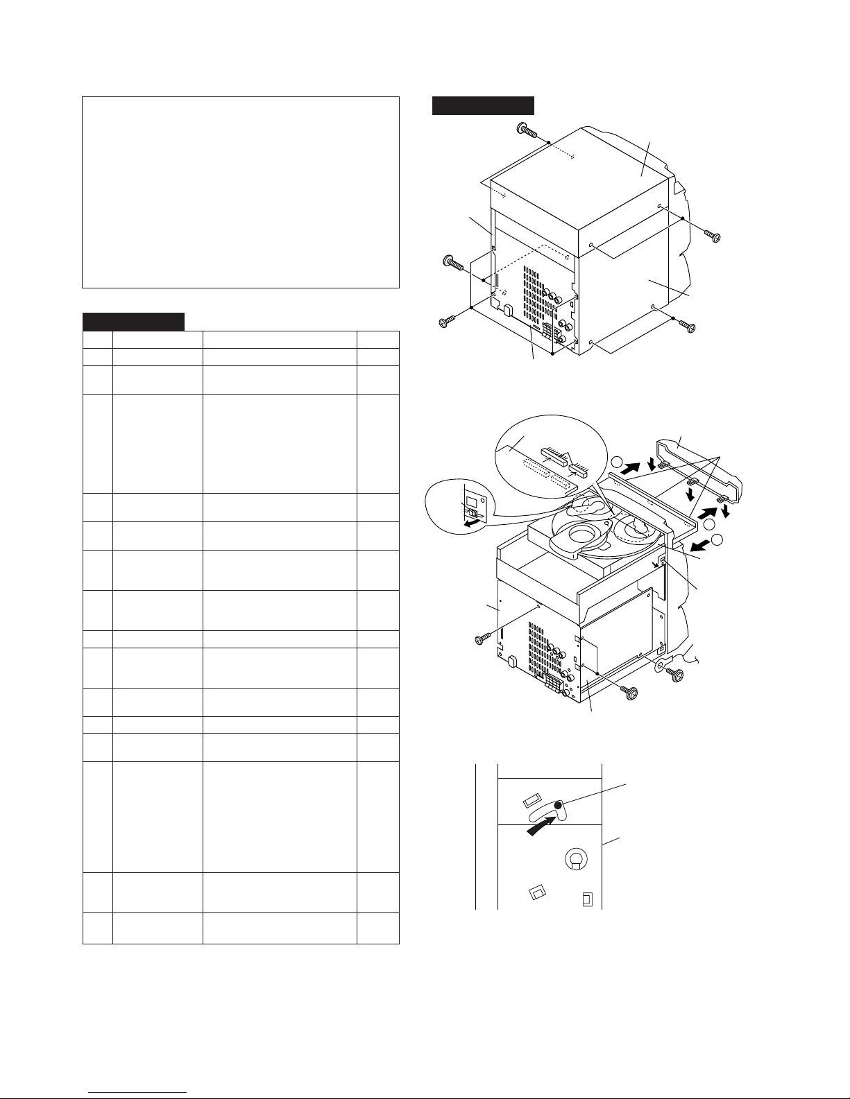
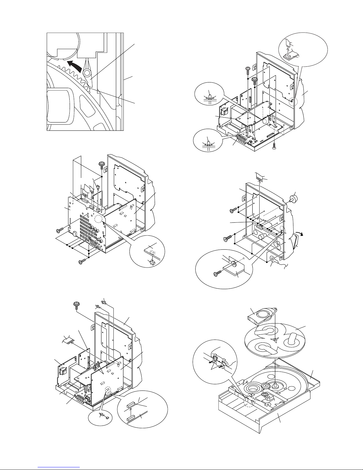
1 Top Cabinet 1. Screw ..................... (A1) x4 12-1
2 Side Panel 1. Screw..................... (B1) x8 12-1
(Left/Right)
3 CD Player Unit/ 1. Turn on the power supply, 12-2
CD Tray Cover open the disc tray, take out
the CD tray cover, and close.
(Note 1)
2. Screw ..................... (C1) x1
3. Hook....................... (C2) x3
4. Hook....................... (C3) x2
5. Socket .................... (C4) x3
12-2,13-2
4 Dolby PWB 1. Screw ..................... (D1) x5 13-2
2. Flat Cable .............. (D2) x2
5 Rear Panel with 1. Screw .................... (E1) x11
12-2,13-2
Fan Motor 2. Socket ..................... (E2) x1 13-2
6 Main PWB 1. Screw ..................... (F1) x2
12-2,13-3
2. Flat Cable .............. (F2) x1 13-3
3. Socket .................... (F3) x6
7 AMP. A/AMP. B 1. Screw ..................... (G1) x4 13-4
PWB with Heat Sink
2. Flat Wire................. (G2) x1
3. PWB Holder ........... (G3) x2
8 Front Panel 1. Screw ..................... (H1) x3 13-4
9 Display PWB 1. Knob........................ (J1) x1 13-5
2. Screw .................... (J2) x13
3. Flat Cable ............... (J3) x1
10 Tape Mechanism 1. Open the cassette holder. 13-5
2. Screw...................... (K1) x5
11
Headphones PWB
1. Screw ..................... (L1) x1 13-5
12 Turntable 1. Hook....................... (M1) x2 13-6
2. Cover ..................... (M2) x1
13 Disc Tray 1.
Turn fully the lock lever in the
12-3
arrow direction
.
2.
While holding the lock lever,rotate
13-1
the cam gear until the cam gear
rib engages with the clamp lever.
3.
Push the slide chissis backward to
14-1
engage the claw with the groove
and remove it in the direction
of the arrow. ...............
(N1) x6
14 CD Servo PWB 1. Screw ..................... (P1) x1 14-2
(Note 2) 2. Hook....................... (P2) x2
3. Socket .................... (P3) x4
15 CD Mechanism 1. Hook....................... (Q1) x2 14-3
2. Hook....................... (Q2) x3
DISASSEMBLY
Caution on Disassembly
Follow the below-mentioned notes when disassembling
the unit and reassembling it, to keep it safe and ensure
excellent performance:
1. Take cassette tape and compact disc out of the unit.
2. Be sure to remove the power supply plug from the wall
outlet before starting to disassemble the unit.
3. Take off nylon bands or wire holders where they need to
be removed when disassembling the unit. After servicing
the unit, be sure to rearrange the leads where they were
before disassembling.
4. Take sufficient care on static electricity of integrated
circuits and other circuits when servicing.
Figure 12-2
Figure 12-3
CD-DD4500
STEP
REMOVAL
PROCEDURE
FIGURE
Figure 12-1
CD-DD4500
Note 1: How to open the changer manually. (Fig. 12-3)
1. In this state, turn fully the lock lever in the arrow direction through
the hole on the loading chassis bottom.
2.
While holding the lock lever, rotate the cam gear anticlockwise until the
cam gear rib engages with the clamp lever.
(Fig. 13-1)
3. After that, push forward the slide Chissis.
Note 2:
1. After removing the connector for the optical pickup from the
connector, wrap the conductive aluminium foil around the front end
of the connector so as to protect the optical pickup from electrostatic damage.
Note 3:
1. Be careful not to break the claw of the CD mechanism.
2. When fining back the cam gear assembly, let it lock by front
movement.
Lock Lever
CD Player Unit
(Bottom View)
(B1) x 4
ø3 x 10mm
(B1) x 2
ø3 x 10mm
Rear
Panel
(B1) x 2
ø3 x 10mm
Side Panel
(Right)
Side Panel
(Left)
(A1) x 2
ø3 x 12mm
(A1) x 2
ø3 x 12mm
Top Cabinet
Pull
(C3) x 1
(C4) x 2
CD Servo
PWB
(C3) x 1
CD Player
Unit
CD Tray Cover
(C2) x 3
1
1
2
(F1) x 1
ø3 x 10mm
Lug Wire
(E1) x 2
ø3 x 10mm
Main PWB
Rear
Panel
(C1) x 1
ø3 x 10mm
Page 13
– 13 –
CD-DD4500
Figure 13-1
Figure 13-2
Figure 13-3
Figure 13-5
Figure 13-6
Clamp Lever
CD Player Unit
(Top View)
Cam Gear Rib
Turntable
Slide
Chassis
(M2) x 1
CD Player Unit
(M1) x 2
Main PWB
Amp. A
PWB
Amp. A
PWB
Amp. B
PWB
(F3) x 1
Main PWB
Transformer
PWB
Front
Panel
(F2) x 1
Power PWB
(F3) x 2
(F3) x 1
(F3) x 1
(F1) x 1
ø3 x 10mm
(F3) x 1
Main PWB
Amp. B
PWB
Dolby
PWB
(E2) x 1
(D2) x 2
(C4) x 1
(E1) x 9
ø3 x 10mm
Rear
Panel
(D1) x 1
ø3 x 10mm
(D1) x 4
ø3 x 10mm
(J3) x 1
(J2) x 13
ø3 x 10mm
(K1) x 5
ø3 x 10mm
(J1) x 1
Display PWB
Headphones
PWB
Open
Cassette
Holder
Tape
Mechanism
(L1) x 1
ø3 x 10mm
Lug Wire
Washer
(H1) x 3
ø3 x 8mm
Headphones
PWB
(G2) x 1
Amp. A
PWB
Amp. B
PWB
Front
Panel
(G1) x 2
ø3 x 6mm
(G1) x 2
ø3 x 10mm
(G3) x 1
PushPush
(G3) x 1
PushPush
Figure 13-4
Page 14
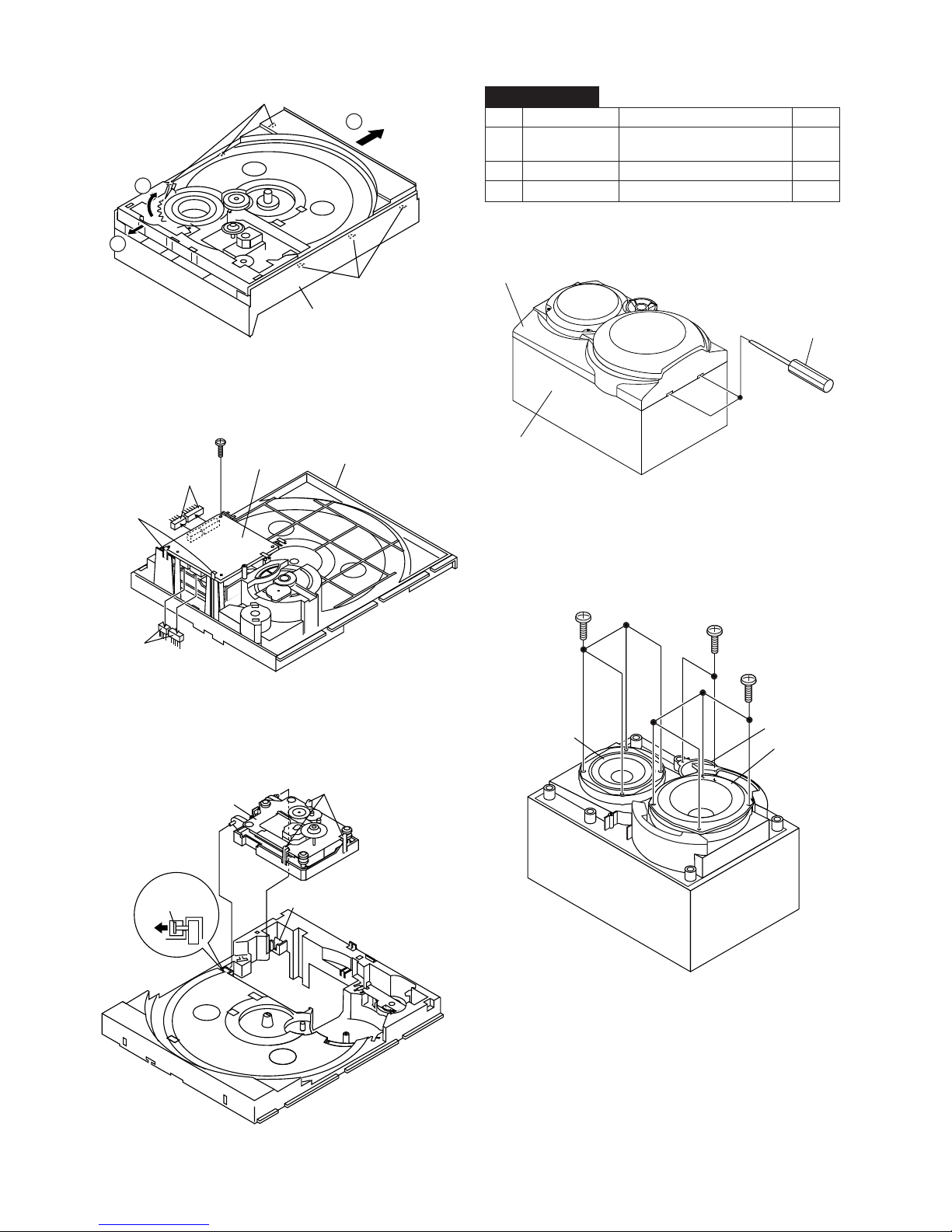
CD-DD4500
– 14 –
Figure 14-2
Figure 14-3
Figure 14-5
(P3) x 2
(P2) x 2
(P3) x 2
CD Servo
PWB
Slide
Chassis
(P1) x 1
ø3 x 8mm
(Q2) x 3
(Q1) x 1
(Q1) x 1
CD
Mechanism
Figure 14-1
1
3
2
(N1) x 3
(N1) x 3
CD Player Unit
(C1) x 2
ø3 x 10mm
Woofer
Subwoofer
Tweeter
(A2) x 4
ø4 x 16mm
(B1) x 4
ø4 x 16mm
1 Subwoofer 1. Front Panel ............ (A1) x1 14-4
2. Screw ..................... (A2) x4 14-5
2 Woofer 1. Screw ..................... (B1) x4 14-5
3 Tweeter 1. Screw ..................... (C1) x2 14-5
STEP
REMOVAL PROCEDURE
FIGURE
Figure 14-4
CP-DD4500
Screwdriver
Driver should
be pried away
from Speaker Box.
(A1) x 1
Speaker Box
Page 15
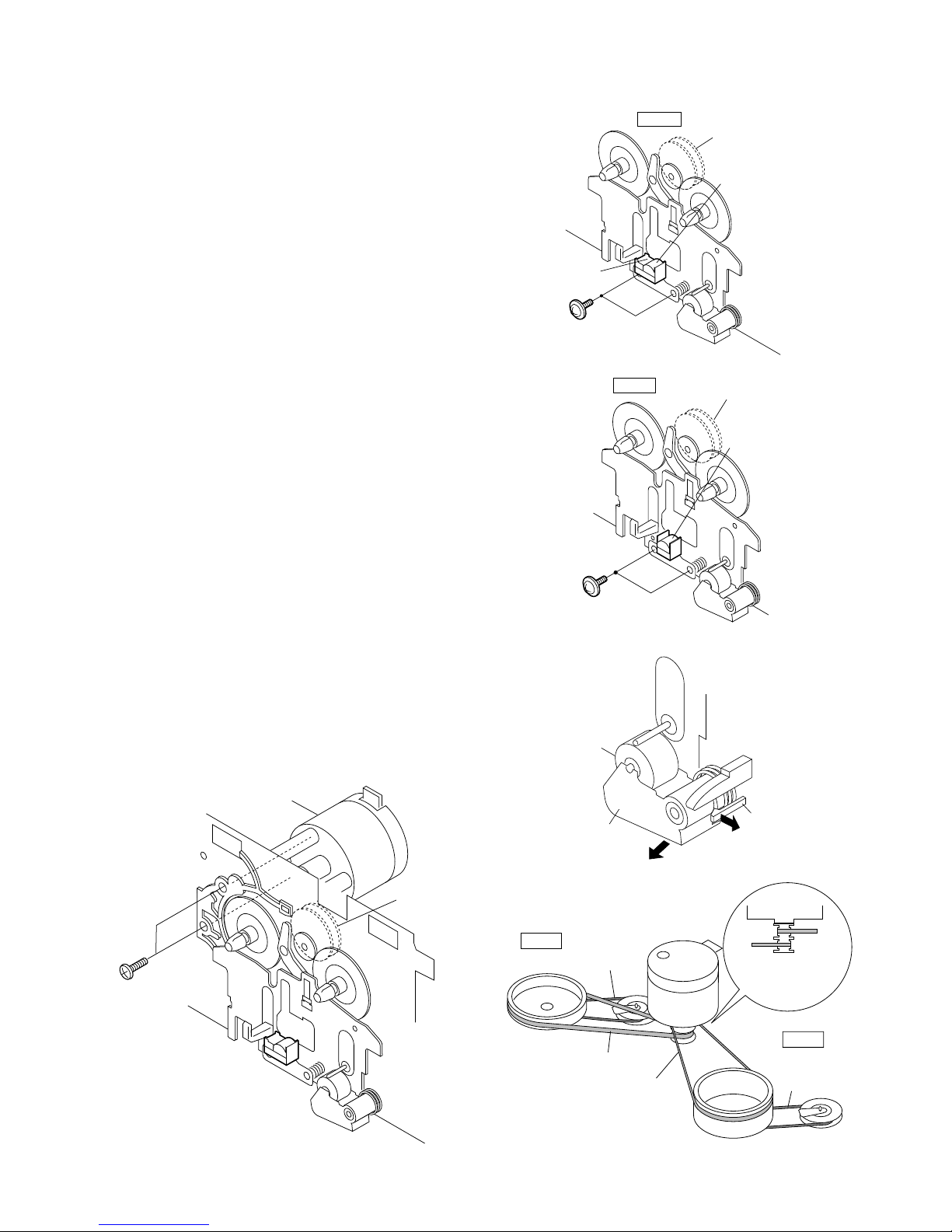
– 15 –
CD-DD4500
REMOVING AND REINSTALLING THE MAIN PARTS
TAPE MECHANISM SECTION
Perform steps 1 to 8 and 10 of the disassembly method to
remove the tape mechanism.
How to remove the record/playback and erase
heads (TAPE 2) (See Fig. 15-1)
1. When you remove the screws (A1) x 2 pcs., the recording/
playback head and three-dimensional head of the erasing
head can be removed.
How to remove the playback head (TAPE 1)
(See Fig. 15-2)
1. When you remove the screws (B1) x 2 pcs., the playback
head.
How to remove the pinch roller (TAPE 1/2)
(See Fig. 15-3)
1. Carefully bend the pinch roller pawl in the direction of the
arrow <A>, and remove the pinch roller (C1) x 1 pc., in the
direction of the arrow <B>.
Note:
When installing the pinch roller, pay attention to the spring
mounting position.
How to remove the belt (TAPE 2) (See Fig. 15-4)
1. Remove the main belt (D1) x 1 pc., from the motor side.
2. Remove the FF/REW belt (D2) x 1 pc.
How to remove the belt (TAPE 1) (See Fig. 15-4)
1. Remove the main belt (E1) x 1 pc., from the motor side.
2. Remove the FF/REW belt (E2) x 1 pc.
How to remove the motor (See Fig. 15-5)
1. Remove the screws (F1) x 2 pcs., to remove the motor.
Figure 15-1
Figure 15-2
Figure 15-3
Figure 15-4Figure 15-5
(A1)x2
Ø2 x 9mm
TAPE 2
Record/Playback
Head
Erase Head
Clutch Ass'y
(B1)x2
Ø2 x 9mm
TAPE 1
Playback
Head
Clutch Ass'y
Pinch Roller
(C1)x1
<A>
<B>
Pinch
Roller
Pawl
Pull
TAPE 2
TAPE 1
Main Belt
(E1)x1
TAPE 2
Main Belt
(D1)x1
TAPE 1
Main Belt
(D1)x1
Main Belt
(E1)x1
FF/REW
Belt
(D2)x1
FF/REW
Belt
(E2)x1
Motor
Motor
(F1) x2
Ø 2.6 x 5mm
Motor
Clutch Ass'y
Page 16
CD-DD4500
– 16 –
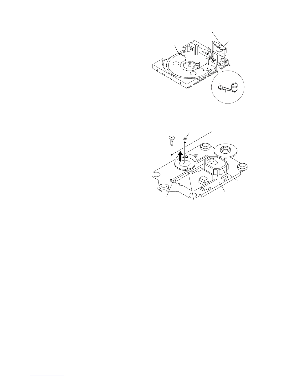
How to remove the pickup (See Fig. 16-2)
1. Remove the stop washer (B1) x 1 pc., to remove the gear
(B2) x 1 pc.
2. Remove the screws (B3) x 2 pcs., to remove the shaft (B4).
3. Remove the pickup.
Note
After removing the connector for the optical pickup from the
connector wrap the conductive aluminium foil around the front
end of connector so as to protect the optical pickup from
electrostatic damage.
Figure 16-2
CD MECHANISM SECTION
Perform steps 1, 2, 3, 12, 13, 14 and 15 of the disassembly
method to remove the CD mechanism.
How to remove the loading motor
(See Fig. 16-1)
1. Bend the hooks (A1) x 5 pcs., to remove the loading motor.
2. Remove the drive belt (A2) x 1 pc.
Figure 16-1
(A1) x 2
(A1) x 1
Loading Motor
Loading
Motor PWB
Slide
Chassis
(A1) x 2
Pulley
Drive Belt
(A2) x 1
Loading
Motor
(B3) x 2
ø2.6 x 6mm
Shaft
(B4) x 1
Stop Washer
(B1) x 1
Gear
(B2) x 1
CD Mechanism
Pickup
Page 17
– 17 –
CD-DD4500
fL: Low-range frequency
fH: High-range frequency
• AM adjustment and confirmation
Figure 17-3 AM IF
TUNER SECTION
• Setting the Test Mode
While holding down the MEMORY/SET button and the XBASS button, press the POWER button. Frequencies are
rewritten in memory as shown in table 17. Call them using the
VOLUMN knob of tuner circuit adjustment and check.
Note that once you reinitialize the settings, the frequencies
recorded by users will be changed.
Preset No. Frequency
P01 87.5 MHz P06 530 kHz
P02 108.0 MHz P07 1,720 kHz
P03 90.0 MHz P08 600 kHz
P04 106.0 MHz P09 1,400 kHz
P05 98.0 MHz P10 990 kHz
Adjusting item
Adjusting object
Adjusting
method
IF Adjust the indication of Set IF wafeform
T351 set to 1,720 kHz.
450 kHz to maximum.
Frequency cover fL: T306 (530 kHz) fL: 1.3 ± 0.1 V
(VT line voltage of Adjust the indication fH: 8.5 ± 1.3 V
TP301) of set to 530 kHz. (Only confirmation)
fH: (1,720 kHz)
Tracking fL: T302 (990 kHz) Set the output of
speaker terminal
to maximum.
AM signal oscillator Frequency 400 Hz, 30 %, AM modulation
• FM mute level adjustment
Frequency
Adjusting
object
Adjusting
method
98.0 MHz 26 dB(EMF) VR351 Input: CNP301
Output: Speaker
Terminal
FM signal oscillator Frequency 1 kHz, 22.5 kHz
Adjusting object
Preset No.
Frequency
Figure 17-2 FM Mute Level
Table 17
Electronic
Voltmeter
GND
AM Loop Antenna
AM signal oscillator
Loop Antenna
UNIT
IF : Speaker Terminal
Frequency cover: TP301
Electronic
Voltmeter
UNIT
FM signal oscillator
CNP301
Speaker
Terminal
• Erasing the registered broadcast station
When the power is off, press and hold the TUNER (BAND)
button and the X-BASS button, and then press the POWER
button.
All the registered stations are erased.
ADJUSTMENT
MECHANISM SECTION
• Driving Force Check
Torque Meter Specified Value
Play: TW-2111 Tape 1: Over 80 g
Tape 2: Over 80 g
• Torque Check
Torque Meter
Tape 2
Play: TW-2111 30 to 80 g.cm 30 to 80 g.cm
Fast forward: TW-2231 — 70 to 180 g.cm
Rewind: TW-2231 — 70 to 180 g.cm
Specified Value
Tape 1
Specified
Value
Adjusting
Point
Instrument
Connection
Test Tape
Normal MTT-111 Variable 3,000 ± 30 Hz Speaker
speed Resistor in Terminal
motor. (Load
resistance:
6 ohms)
• Tape Speed
Figure 17-1
TAPE MECHANISM
Tape
Motor
Variable Resistor in motor
Page 18
CD-DD4500
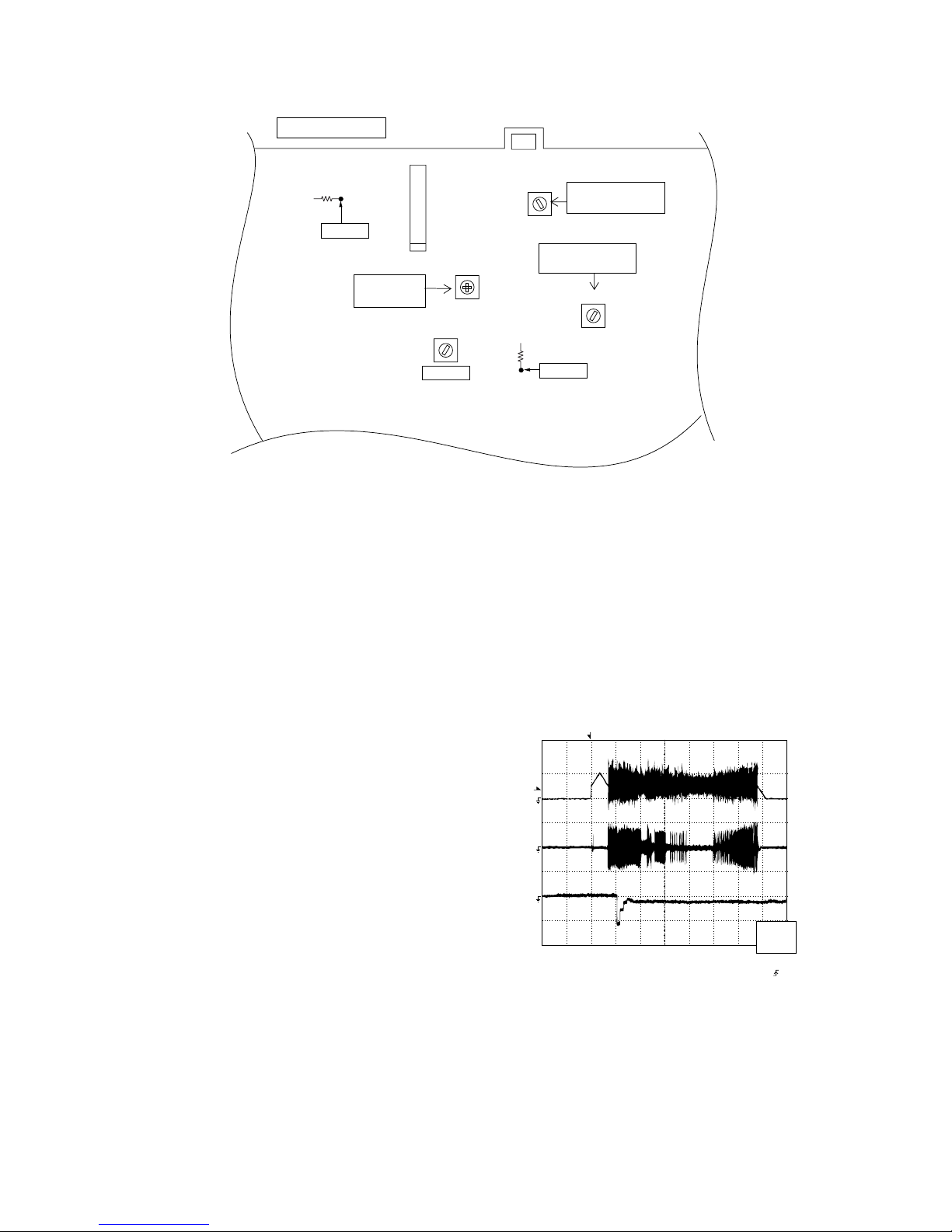
– 18 –
CD SECTION
Figure 18-2
Items adjusted automatically
(1) Offset adjustment (The offset voltage between the head
amplifier output and the VREF reference voltage is
compensated inside the IC.)
* Focus offset adjustment
* Tracking offset adjustment
(2) Tracking balance adjustment (waveform drawing
Fig.18-2 EFBL)
(3) Gain adjustment (The gain is compensated inside the IC
so that the loop gain at the gain crossover frequency will
be 0 dB.)
* Focus gain adjustment
* Tracking gain adjustment
• Adjustment
Since this CD system incorporates the following automatic
adjustment functions, readjustment is not needed when
replacing the pickup. Therefore, different PWBs and pickups
can be combined freely.
Each time a disc is changed, these adjustments are
performed automatically. Therefore, playback of each disc
can be performed under optimum conditions.
T
T
EFBL
FDO
TE
Stopped
CH1=500 mV
DC 10:1
CH2=200 mV
DC 10:1
CH3=1 V
DC 10:1
500 ms/div
(500 ms/div)
NORM:20 kS/s
1
2
3
=Record Length=
Smoothing : ON CH1 : 0.000 V
CH2 : 0.000 V
Main : 100 K
Zoom : 2 k
Mode : SINGLE
Type : EDGE CH1
Delay : 0.0 ns
Hold off : 0.2 µs
CH3 : 0.00 V
CH4 : 0.00 V
BW : FULL
=Trigger==Filter= =Offset=
CH2
v/DIV
200 mV
1999/04/05 20:26:47
Figure 18-1 ADJUSTMENT POINTS
FE301
AM IF
T302
T306
T351
AM
TRACKING fL
AM BAND
COVERAGE fL
FM MUTE
LEVEL
MAIN PWB
CNP301
FM/AM LOOP
ANTENNA
VR351
TP302
R350
R345
TP301
Page 19
– 19 –
CD-DD4500
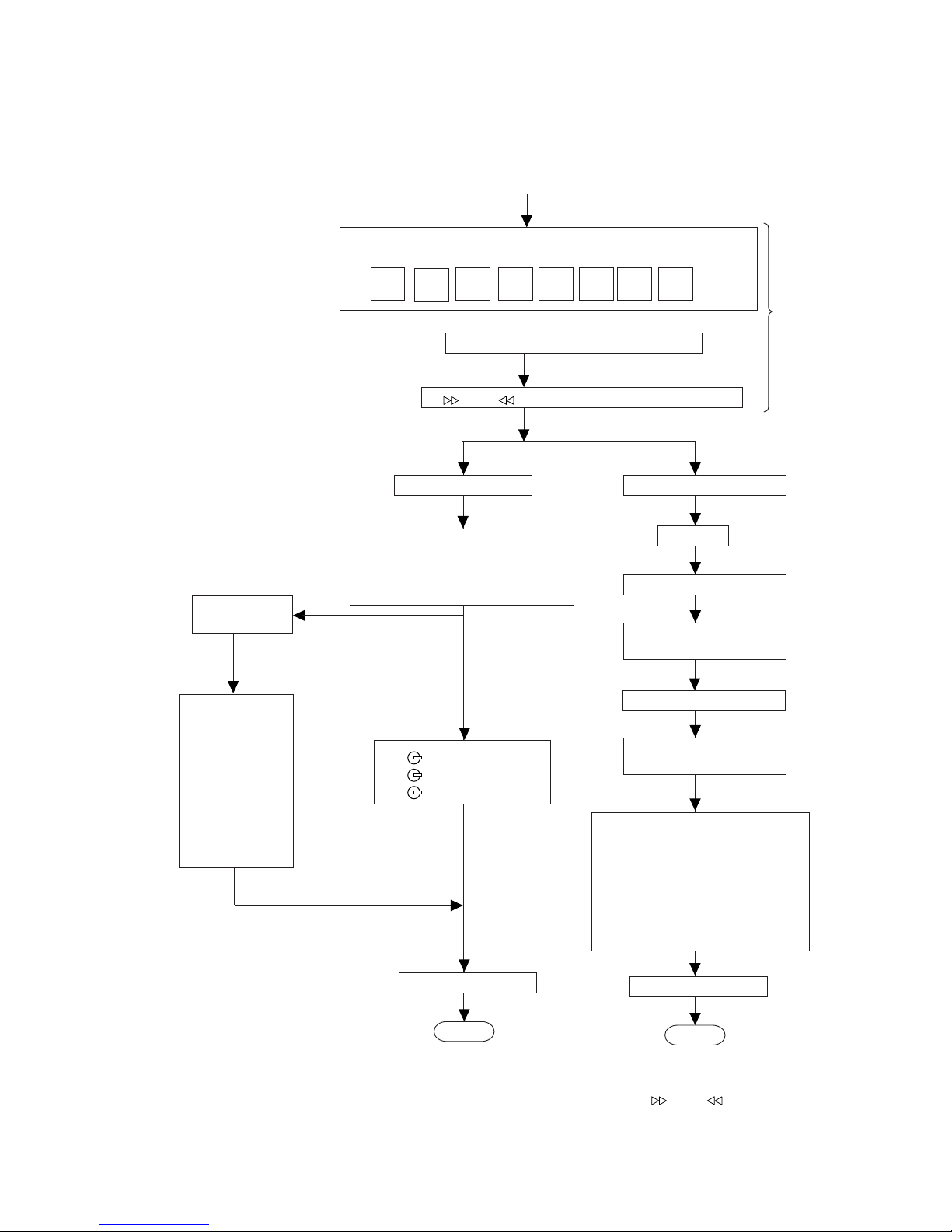
TEST MODE
• Setting the test mode
Any one of test mode can be set by pressing several keys as follows.
<X-BASS> + <CD> + <POWER> TEST: CD operation test.
Function:-CD test mode.
-Enter test mode.
C D T E S T
OPEN/CLOSE operation is using manual.
<< >>, << >> buttons make pick's slide possible.
Do TOC IL. Do normal play.
When these following key is input
into PLAY key, track number can
be appoint directly.
<<PLAY>> key input.
<<MEMORY>> key input.
<< 1>> key: Track 4
<< 2>> key: Track 9
<< 3>> key: Track 15
<<STOP>> key input.
STOP
Laser ON.
<<MEMORY>> key input.
Tracking OFF play at that
specific point.
<<MEMORY>> key input.
Tracking ON play from
that specific point.
<<STOP>> key input.
STOP
IL isn't done
VOL — Last memory
BAL — CENTER
P.GEQ — FLAT
X-BASS — OFF
To cancel : Power OFF
Sliding the PICKUP with
<<
>>, << >> button
must only be in STOP mode.
<<MEMORY>>
key input.
Adjustment result
automatically will
display as below.
for each 2 sec :
a) "FOFF_XX"
b) "TOFF_XX"
c) "TBAL_XX"
d) "TGAN_XX"
f) "FGAN_XX"
g) "RFLS_XX"
explanation:
a) Focus off set ="FOFF_XX"
b) Tracking off set ="TOFF_XX"
c) Tracking balance ="TBAL_XX"
d) Tracking Gain ="TGAN_XX"
f) Focus Gain ="FGAN_XX"
g) RF level shift ="RFLS_XX"
Adjustment result automatically will
display as below for each 2 sec :
a) "FOFF_XX"
b) "TOFF_XX"
c) "TBAL_XX"
d) "TGAN_XX"
f) "FGAN_XX"
g) "RFLS_XX"
Page 20

CD-DD4500
– 20 –
Standard Specification of Stereo System Error Message Display Contents
Error Contents DISPLAY Notes
Output while Device Protection Operation. TIMER LED While in Protect Circuit Operate.
FLASHING Over Current Detection.
DC Detection.
TAPE Mechanism Error. 'ER-TA**' 00: Tape Mechanism Error.
01: Initial Error.
02:
03:
CD/VCD Pickup Mechanism Error. 'ER-CD**' 00: Pickup Mechanism Error.
01: PU-IN SW Detection NG.
02:
03:
04:
CD Changer Mechanism Error. 'ER-CD**' 10: Changer Error.
11: Initial Error.
12:
13:
Tray Error. 'ET-CD**' 20: Tray Error.
21:
22:
23:
Focus Not Match. 'NO DISC'
IL Time Over. 'NOT READ'
TUN PLL Unlock. 'ER-TU**' 00: TUN Error.
01: PLL Unlock.
02:
03:
Page 21
– 21 –
CD-DD4500
Figure 21 BLOCK DIAGRAM (1/3)
+3.3V
+5V
CNS4
BI4
CNP4
M3
T/T UP DOWN
LOADING
+3.3V
TO DISPLAY SECTION
TO MAIN SECTION
CONSTANT
VOLTAGE
Q2
LASER
DRIVER
+3.3V
Q1
+5V
PICK UP UNIT
IC1
LC78645E
CD SERVO
VVDD
LDD
LDS
M
SW3
DISC
NUMBER
SW2
CLAMP
SW1
OPEN/
CLOSE
CNP8
CNP7
TRACKING COIL
FOCUS COIL
SW4
PICK UP
IN
M2
SLED
MOTOR
M1
SPINDLE
MOTOR
M
M
R-CH
Q3
XVDD
RVDD
LVDD
ADAVDD
RFVDD
XL1
33.8688 MHz
OC. DISC NO
CLAMP SW
CD RES
CLK
DI
DO
CE
DRF
WRQ
+5V (+B5)
+5V (+B5)
DGND
L-CH
AGND
VCC3
VCC2
VCC4
VCC1
IC2
M63001FP
FOCUS/TRACKING/
SPIN/SLED
DRIVER
XIN
XOUT
RES
WRQ
DO
DI
CLK
CE
TIN2
TIN1
FIN2
FIN1
TD0
FD0
SPDO
SLDO
CONT5
CONT5
BI7
CONT2
CONT3
CONT4
RCHO
RVSS
LVSS
LCHO
80
42
79
75
20
5
40
18
24
23
14
8
21
22
29
35
41
47
46
7
10
987
15
1
2
1
2
17 25
42
41 8339
4765
168226 27
316452
316452
316452
54
71
61
62
63
69
57
56
55
51
50
40
39
37
19
28
26
23
22
21
3271689
615432
4543 44 25 70
64
65
66
48
49
18
Page 22
CD-DD4500
– 22 –
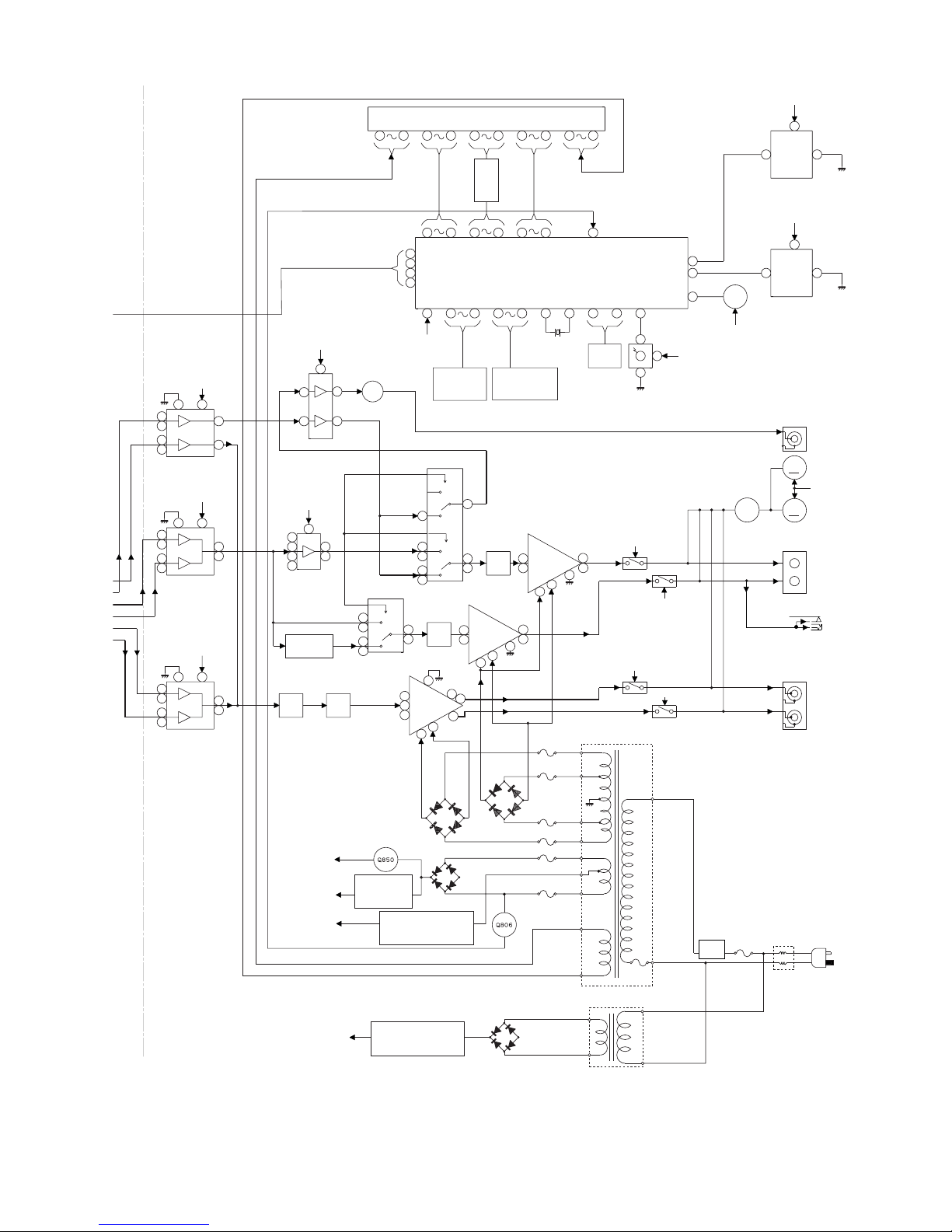
Figure 22 BLOCK DIAGRAM (2/3)
IC501
TORX178B
OPTICAL FIBER
DATA LINK
3
2
1
X501
2.2MHz
IC602
M62446FP
6-CH ELECTRONIC
VOLUME
42
36
35
34
33
32
31
15
13
12
11
9
8
6
IC6
0
NJM4
5
BUFFE
R
I
C
NJ
M
BUFF
E
I
C
NJ
M
BUF
F
6
5
4
3
2
6
5
4
3
2
6
5
4
3
2
IC502
74VHC00F
INVERTOR
14
12
9
7
6
IC505
AK4527BVQ
6-CH CODEC IC
39
37
36
32
30
28
27
26
25
24
23
16
9
4
IC504
IX0443AW
DOLBY DECODER
99
98
97
95
81
71
62
53
49
47
35
34
XI
XO
VSSX
VSSDL
VSS
VSS
VSS
CKO
VSS
VSS
VDD
VCC
GND
VDD
VDD
RX
24
22
18
14
13
21
4
FE301
FM FRONTEND
8
5
4 32
1
IC303
LA1832S
FM IF DET./FM MPX./AM IF
23
21
18
17
16
15
14
13
12
9
8
7
5
4
21
IC302
LC72131
PLL(TUNER)
22
21
20
17
16
15
11
10
9
7
6
5
43
1
IC102
BA3126N
HEAD
SELECTOR
9
8
7
6
5
4
3
2
1
IC601
LC75341
AUDIO PROCESSOR
JK601
VIDEO IN
AUX
TAPE
VSS VDD
TUNER
AUX
+B4
+B4
+B5
+B5
+B5
16
10
15
14
11
9
3
23
P.B.
REC
AC BIAS
RECORD/
PLAYBACK HEAD
ERASE HEAD
TAPE 2
PLAYBACK
HEAD
TAPE 1
L-CH
R-CH
L-CH
R-CH
BIAS OSC
Q128
L104
BIAS
Q126
Q101
Q102
Q121
Q122
SWITCHING
Q124
L103
SWITCHING
MUTING
IC101
PLAYBACK AND RECORD
/PLAYBACK AMP.
PB
R
L
REC
REC
R
L
L NF
R NF
ALC
REC
T1/T2
T1/T2
NOR/
HIGH
REF
R REC
L REC
POP REDUCE
R NF
L NF
L(T2)
R(T2)
R(T1)
L(T1)
1
24
2
23
3
22
6
9
16
14
12
15
19
10
17
18
8
7
20
5
21
13
4
H/N
+B4
+B4
+B4
+B4
SWIN
SW_OUT
DVDD
DVSS
LIN+
RIN+
C_OUT
L_OUT
R_OUT
SL_OUT
ROUT2
ROUT3
LOUT3
LOUT2
ROUT1
LOUT1
SR_OUT
SR_IN
C_IN
R_IN
L_IN
GND_R
SL_IN
FROM CD SECTION
CNP7
AM
CNP301
FM
AM MIX
CF303
AM RF IN
AM OSC IN
AM IF
450 kHz
FM/AM
OUT
MPX IN
STEREO
FM+B
GND
AM IF
CF352
T351
10.7 MHz
FM/AM
MO/ST
VCO
CF351
R
L
X351
456kHz
FM/AM
MO/ST
VT
OSC
X352
4.5 MHz
CLK DODI
CE
SWITCHING
FM
Q360
AM BAND
COVERAGE
AM TRACKING
T303
T306
6 7
VCC
+B4
L
R
L
R
L
R
L
R
TO IC181
Q102
MOTOR
DRIVER
Q102
TAPE 1
SOLENOID DRIVER
Q102
TAPE 2
SOLENOID DRIVER
+B3
+B3
+B3
TAPE
MECHANISM
ASS'Y
Page 23
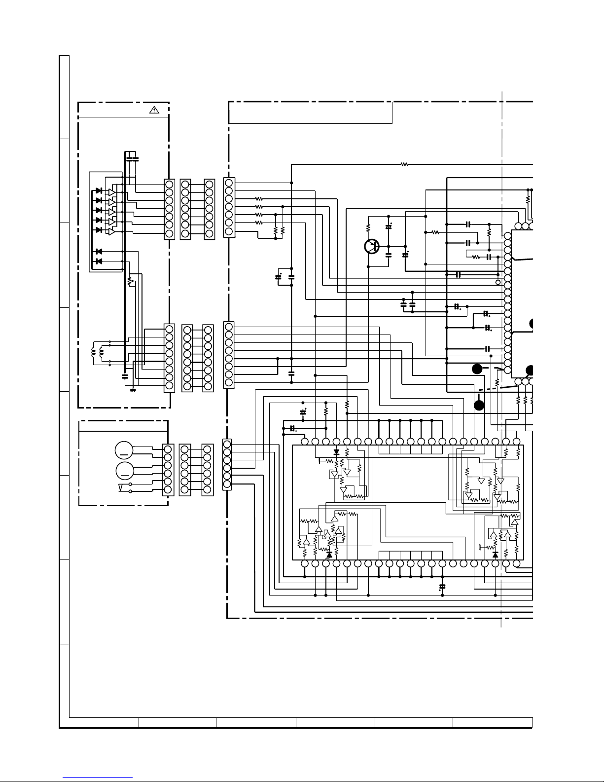
– 23 –
CD-DD4500
Figure 23 BLOCK DIAGRAM (3/3)
18
4 1
18
41
IC181
BU2092F
INPUT/OUTPUT
EXPANDER
IC702
BU2092F
INPUT/OUTPUT
EXPANDER
15
14
13
5
4
1
2
3
IC606
NJM4565M
BUFFER AMP
IC605
NJM4565M
BUFFER AMP
IC607
NJM4565M
BUFFER AMP
8
7
6
5
4
3
2
1
8
7
6
5
4
3
2
1
8
7
6
5
4
3
2
1
IC905
TC4053BP
TRIPLE 2 CH
MULILPEXER
IC906
TC4053BP
TRIPLE 2 CH
MULILPEXER
14
13
12
5
4
3
IC904
KIA4558P
OPE AMP.
IC703,IC704
KIA4558P
OPE AMP.
8
7
6
5
3
2
1
IC907
KIA4558P
OPE AMP.
8
7
5
3
1
RX701
REMOTE SENSOR
3
2
1
XL701
4.194304MHz
JOG701
JOG
VOLUME
IC701
IX0442AWZZ
SYSTEM MICRCOMPUTER
100
93
28
29
30
31
92
87
86
79
60
49
48
42
27
26
25
17
16
9
7
5
3
1
FL701
FL DISPLAY
58
56
53
29
19
14
13
6
31
SOC901
SUBWOOFER
PRE OUT
M
M
SO901
SPEAKER
TERMINAL
SOC401
SPEAKER JACK
D802
D801
D806
D804
D803
D805
D881
D882
D884
D883
T.F.
AC120 V/60 Hz
AC POWER
SUPPLY CORD
F801
6.3A/125V
T801
MAIN POWER TRANSFORMER
T802
SUB POWER TRANSFORMER
F804
6.3A/125V
F802
4A/125V
F803
4A/125V
F805
6.3A/125V
F806
2A/125V
F807
2A/125V
IC851
KIA7805AP
CONSTANT VOLTAGE
REGULATOR
IC850
KIA7810AP
VOLTAGE
REGULATOR
IC880
KIA7805AP
CONSTANT VOLTAGE
REGULATOR
+B6 5V
+B4 A_+10V
+B3 M_+12V
+B5 5V
VF1
VF2
-VF
+B1
+B2
–B1
–B2
IC401
STK40224
POWER AMP.
IC901
STK40270N
POWER AMP.
IC902
STK40270N
POWER AMP.
L
L
L
L
L
R
R
R
R
R
10
10
13
18
16
13
13
15
6
6
10
6
9
1
1
15
1
15
8
9
8
9
8
RY402
RY401
RY902
RY901
SURROUND
SUBWOOFER
MAIN
CENTER
Q403
Q404
Q408
Q906
Q907
Q905
Q908
Q401
Q402
Q407
SYSTEM
MUTE
HIGH PASS
FILTER
SYSTEM
MUTE
SYSTEM
MUTE
SYSTEM
MUTE
20ATT
M402
FAN MOTOR
FAN MOTOR
DRIVER
M401
FAN MOTOR
Q423
+B4
+B4
+B4 7 V
+B4
+B6
+B4
+B6
+B5
+B5
+B5
Q917
KEY
SW701-SW712
SW714-SW716
SW722-SW729
SW731-SW734
Q707
LCK
VSS
VDD
LCK
VSS
VDD
AVDD
X1
X2
JOG_0
JOG_1
VLOAD
REMOCON
PSEANA
KEY
CE
CLK
DI
DO
-VF
VF1
VF2
LCK1
LCK2
ERSET
Q701
Q702
Q703
Q704
Q705
Q706
JK701
HEADPHONES
+B3
+B3
+B3
+B3
+B3
RY801
L802
LINE
FILTER
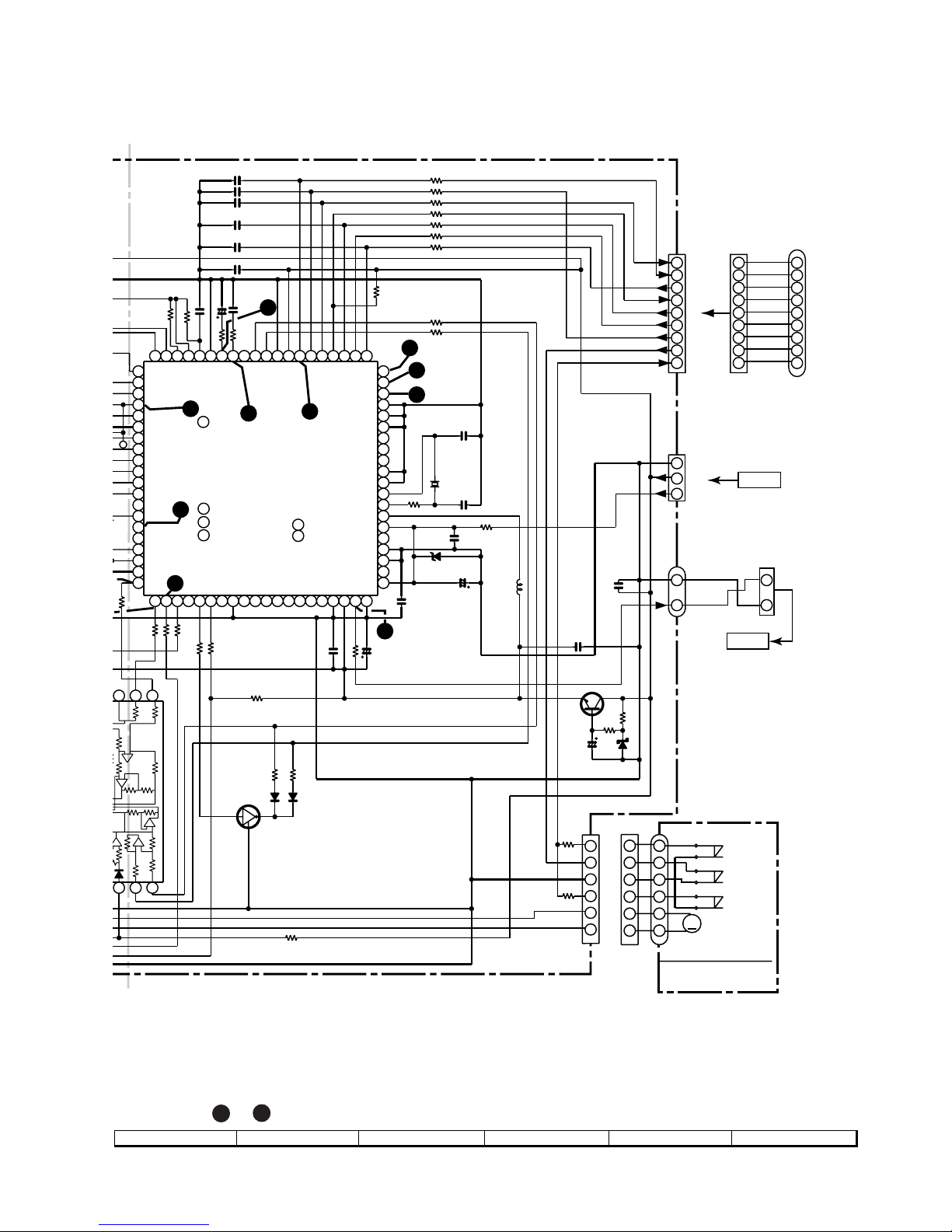
Page 24
CD-DD4500
– 24 –
Figure 24 SCHEMATIC DIAGRAM (1/14)
A
B
C
D
E
F
G
H
1
23456
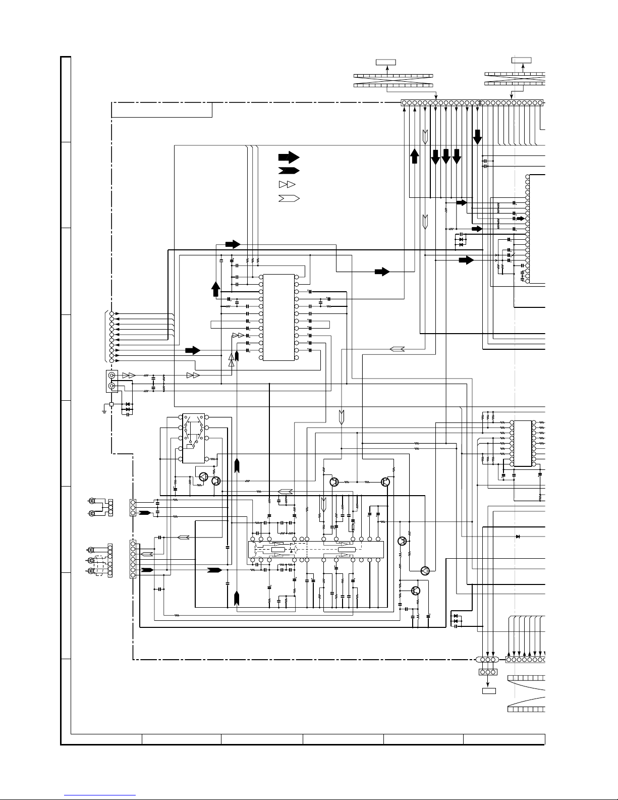
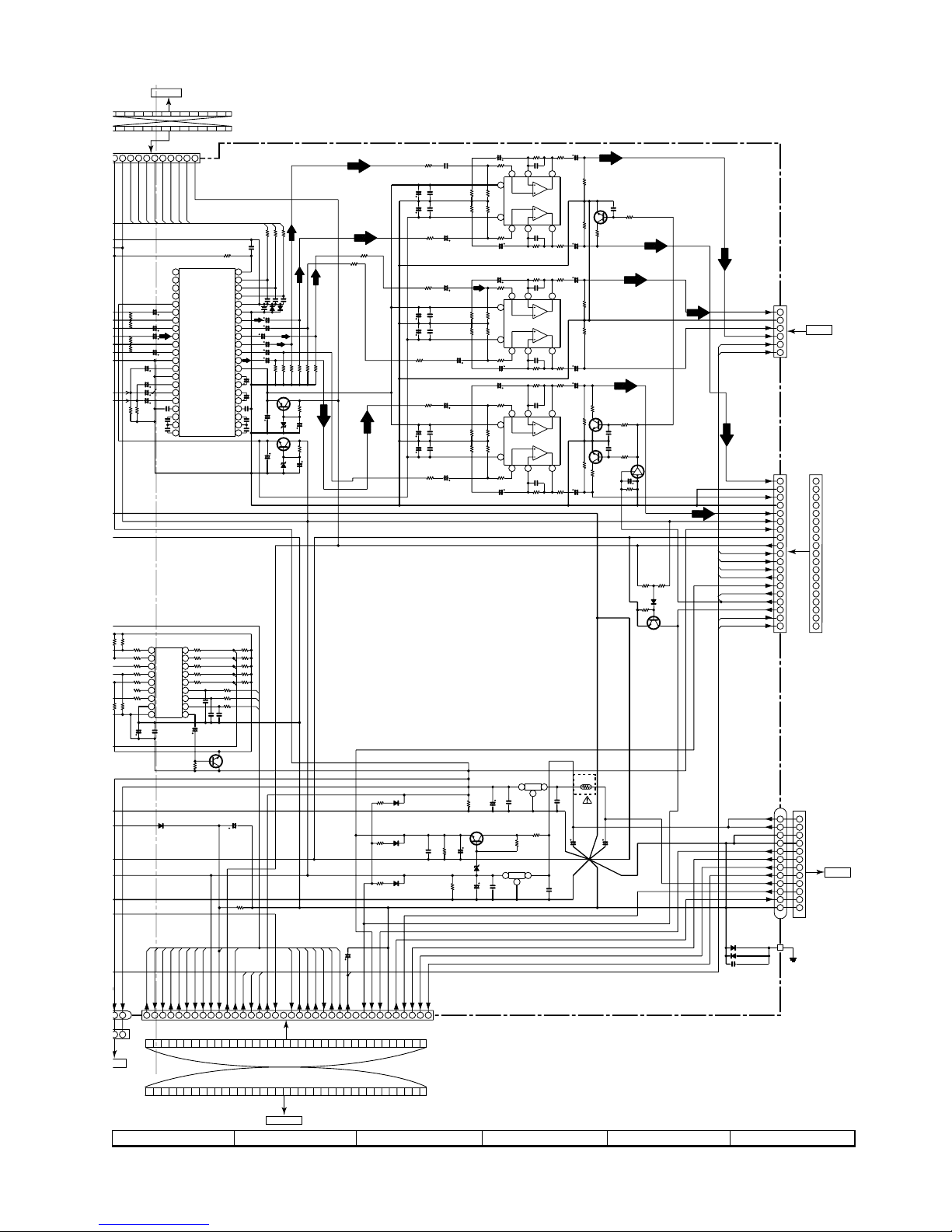
• NOTES ON SCHEMATIC DIAGRAM can be found on page 49.
CD SERVO PWB-C
4
2
1
6
4
8
5
2
1
7
3
6
5
3
6
2
7
1
4
C
F
B
A
E
VREF
VCC
GND
FO–
LD
VR
PD
FO+
TR+
TR–
2
5
1
4
3
6
GND
PUIN
SL+
SL–
SP–
SP+
22 23 24 25 26 27 28 29 30 31 32 33 34 35 36 37 38 39 40 41 42
LD_M+
LD_M–
VCC4
M–
M+
VCC3
SPO
VCC2
SP–
SP+
+
+
–
+
–
+
–
+
–
–
+
–
+
–
+
–
1234
5
6
7
8
9
101112131415161718192021
SLDO
VCC
STANDBY
VREF
MUTE
TO
FD
SL–
SL+
TR–
TR+
FO+
FO–
GND
9
10
11
12
13
14
15
16
17
18
19
20
21 22 2
3
787980
8
7
6
5
4
3
2
1
TP1
TDO
REF1
VREF
ADAVS
S
ADAVD
D
JITTC
RFMO
N
TE
TEC
FE
TIN2
F
TIN1
E
FIN2
B
FIN1
A
RSVS
S
RFVD
D
RF
EFMIN
SLCIS
T
SLCO
5
3
6
2
7
1
4
CD MOTOR PWB-G
GND
FO–
PICKUP UNIT
TR–
TR–
TR+
TR+
FO+
FO+
FO–
PD
VR
LD
F
C
B
A
E
VCC
VREF
SLIDE
SPIN
+
+
–
–
PU-IN
1
2
3
4
5
6
1
2
3
4
5
6
5
3
6
2
7
1
4
5
3
6
2
7
1
4
5
3
6
2
7
1
4
4
1
3
6
5
2
M
M
4
8
5
2
1
7
3
6
4
8
5
2
1
7
3
6
4
8
5
2
1
7
3
6
IC2
M63001FP
LDD
LDS
CT1
0.001
CT2
0.001
R65
3.3K
C49
47/25
C50
22P(CH)
C12
100P
CNP1
C8
0.0047
C11
0.22/50
R14
1K
R15
1K
R9
3.3
R6 22K
R5 8.2K
R4 8.2K
R3 22K
R1
8.2K
C2
0.01
C1
47/25
C38
0.01
CNP2
Q1
KTA1266 GR
R7
47
R11
10K
R2
8.2K
CNP3
R44
12K
C39
100/10
C40
220/6.3
C41
100/10
R13
1K
C3
47/25
C4
0.001
C10
10/50
R12
330
C5
0.047(ML)
C6
0.1
C9
100/10
R10
27K
R42
1.2K
R41
CNS1A
CNS1B
CNS2A
CNS2B
CNS3A
CNS3B
M1
SPINDLE
MOTOR
M2
SLED
MOTOR
SW4
PICKUP IN
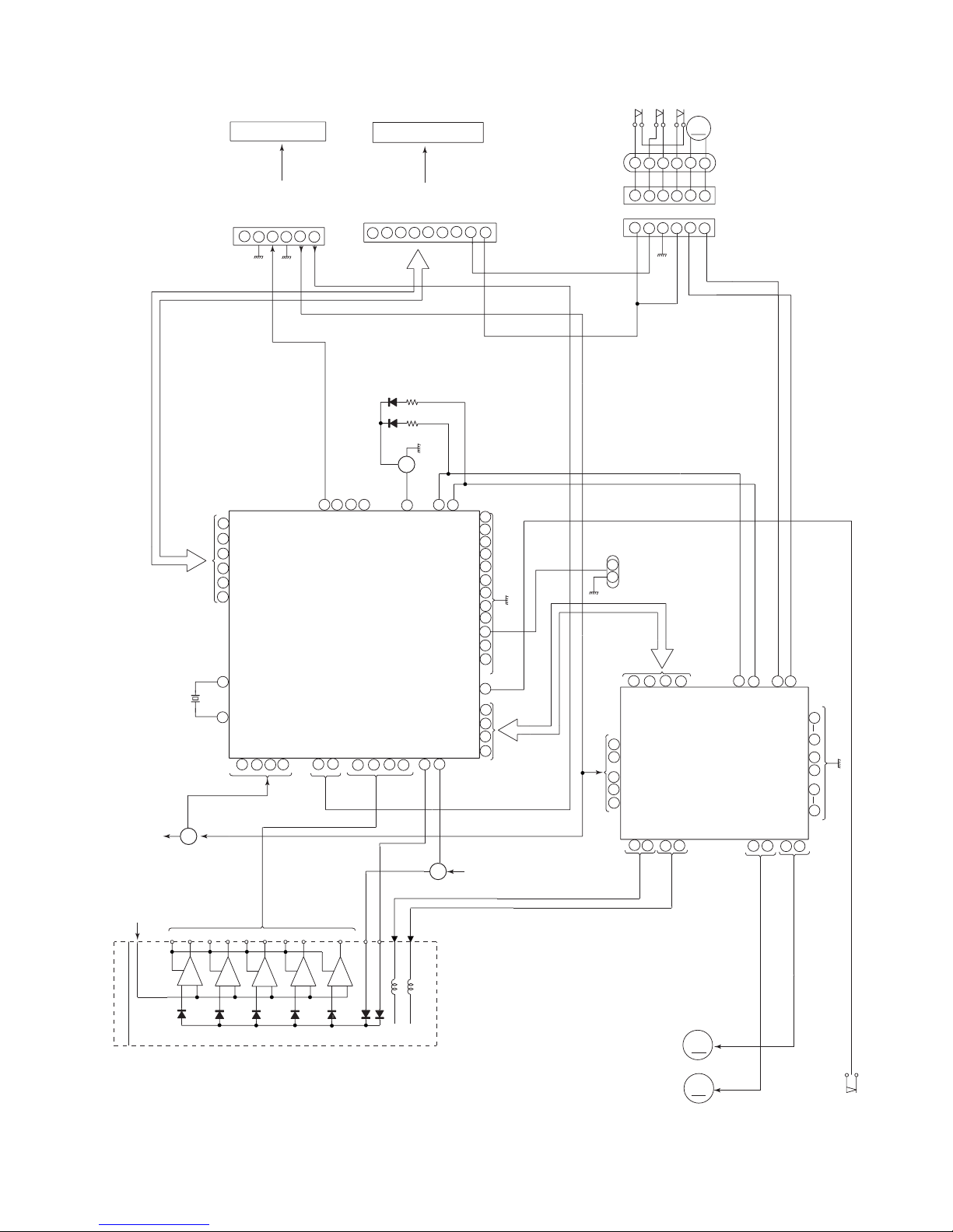
Page 25
– 25 –
CD-DD4500
Figure 25 SCHEMATIC DIAGRAM (2/14)
7
8 9 10 11 12
• The numbers 1 to 12 are waveform numbers shown in page 50.
5
4
6
10
11
12
3
7
8
40 41 42
LD_M+
LD_M–
VCC4
123
TO
FD
3
5
4
2
6
1
DIGITAL
OUT
DGND
2
1
2
1
3
2
1
+5V
+5V
DGND
CD RES
O/C,
DISC NO
CLAMP SW
CL
DI
DO
CE
DRF
WRQ
9
10
11
12
13
14
15
16
17
18
19
20
21
22
23
21 22 23 24 25 26 27 28 29 30 31 32 33 34 35 36 37 38 39 40
41
42
41
42
43
44
45
46
47
48
49
50
51
52
53
54
55
56
57
58
59
60
616263646566676869707172737475767778787980
8
7
6
5
4
3
2
1
FR
TP1
VVDD
PCKIST
VVSS
PDO2
PDO1
CONT2
CONT3
VSS
VDD5
DRF
VRES
VWRQ
DATA
DATACK
LRSY
ASDFIN
ASDACK
ASLRCK
IGMOUT
EFLG
C2F
XVSS
FSX/16MIN
XIN
XOUT
XVDD
RVDD
RCHO
RVSS
LVSS
LCHO
LVDD
TEST
DOUT
VDD
VSS
MON15
MON14
MON13
MON12
MON11
FSEQ
V/1P
DEFECT
SBCK/FG
CONT5
CONT4
GPDAC
SLDO
SPDO
FDO
TDO
REF1
VREF
ADAVSS
ADAVDD
JITTC
RFMON
TE
TEC
FE
TIN2 F
TIN1 E
FIN2 B
FIN1 A
RSVSS
RFVDD
RF
EFMIN
SLCIST
SLCO
9
8
7
6
2
4
5
3
1
9
8
7
6
2
4
5
3
1
1
2
3
4
8
6
5
7
9
M
3
5
4
2
6
1
3
5
4
2
6
1
CD LOADING
MOTOR PWB-E
CNP501
TO
DOLBY PWB
P32 1-B
CNS606
FROM
MAIN PWB
P26 6-H
CNS703
BI703
FROM
DISPLAY
PWB
P29 7-H
1
3
2
9
LDD
LDS
DO
DI
CL
CE
C16
10/16
CNP7
C51
0.022
C19
15P
C20
15P
C36
2.2/50
C48
0.022
C44
0.001
C17
0.022
R43
220
R47
100
C18
100/10
ZD2
DZ3.9BDB
R49
1
R30
8.2K
R19
15K
R31
1K
R14
1K
R16
1K
R15
1K
R20
10K
C14
100/10
XL1
33.8688 MHz
R32 1K
R29
2.2K
R28
2.2K
C27 0.022
R11
10K
C28 100P
1K
D2
D1SS133
D1
D1SS133
R46
470
R45
470
Q3
KRC102 M
R39
680
C35
0.047
(ML)
R37 1K
R36 1K
R35 1K
10
0/50
R34 1K
R40
680
C37
0.1
R17
1K
R33 1K
C33 100P
C30 100P
R38 1K
ZD1
DZ3.3BSB
R22
100
R21
C13
0.022
R18
1K
C32 100P
C34 100P
R42
1.2K
R41
12K
CNP4
L1
0.82µH
Q2
KTC3203 Y
R23
220
CNP8
BI7
CNS7
IC1
LC78645NE
CD SERVO
IC2
M63001FP
FOCUS/TRACKING/
SPIN/SLED DRIVER
BI4
M3 T/T
UP DOWN
LOADING
SW1
OPEN/CLOSE
SW2
CLAMP
SW3
DISC NO.
CNS4
Page 26
CD-DD4500
– 26 –
A
B
C
D
E
F
G
H
1
23456
• NOTES ON SCHEMATIC DIAGRAM can be found on page 49.
Figure 26 SCHEMATIC DIAGRAM (3/14)
0V
0V
0V
0V
2
1
3
11.6V
0V
11.6V
11.7V
0V
0.7V
0V
0V
0V
0V
0.7V
1
2
3
4
5
6
7
8
9
10
+B
+B
+B
+B
+B
+B
+B
+B
-B
+B
+B
VIDEO IN SIGNAL
RECORD SIGNAL
PLAYBACK SIGNAL
FM SIGNAL
D604 DS1SS133
L
NC
A_GND
TUN_L
TUN_R
CE
TUN_SM
CLK
DO
TO
TUNER PWB
P37 11-H
DI
A_+10V
D_GND
VIDEO
R-CH
L-CH
IN
CHASIS
L-CH R-CH
A_GND
T1_L
T1_R
1
2
3
A_GND
R-CH
L-CH
ERASE HEAD
T2_L2
T2_L1
T2_R1
T2_R2
ERASE
M_GND
7
1
2
5
6
3
4
TAPE 1
PLAYBACK HEAD
TAPE 2
RECORD/
PLAYBACK HEAD
123
24
23
22
21
20
19
18
4
5
6
7
17
16
15
14
8
9
10
11
13
12
Hich=T1
–
+
+
–
Nor/CrO2
RIPPLE
ALC
Vcc
ALC
112K
56K
Hich=CHROME
112K
56K
–
–
+
+
GND
R
R
9
8
7
6
2
3
1
5
4
3
2
1
CLK DICE
24
23
22
21
20
19
18
17
16
15
14
13 12
11
10
9
8
7
6
5
4
3
2
1
DVD
TUNER
DECK
AUX
DI
CE
VSS
LOUT
LBASS
LTRE
LIN
L4
L3
L2
L1
CLK
VDD
VREF
ROUT
RBASS
RTRE
RIN
RSEL0
R4
R3
R2
R1
LSEL0
A-13V
DD_STATUS
LOCK
DDAC
DDLAT
RESET
R_OUT
L_OUT
A_GND
L_S
CENTER
A_GND
R_S
A_GND
A_GND
SW
R_F
A_GND
L_F
A_GND
A_GND
DIO
CK
DDCE
A_10V
D_5V
D_GND
A_+B
TO
CD SERVO
PWB
P25 12-D
CD_+B
CD_GND
1
3
2
DD_STATU S
DD_LP
DD_ACK
DD_DIO
DD_LOCK
DD_CS
DD_CLK
TUN_SM
1 3 4 5 7 86 2
18
17
16
15
14
13
12
11
10
9
8
7
6
5
4
3
2
1
Q10
VDD
__
OE
Q11
Q9
Q8
Q7
Q6
Q5
Q4
Q3
Q2
Q1
Q0
LCK
CLOCK
DATA
VSS
21
20
19
18
17
16
15
14
13
12
11
10
9
8
7
6
5
4
3
2
1
L_BASS1
L_BASS2
L_BASS3
L_TRE
BYPASS_
L
BYPASS_
R
L_IN
GND
R_IN
GND_R
C_IN
C_GND
SL_IN
SR_IN
S_GND
SWIN
AVDD
1
3
2
FAN_CTL
DD_RST
–11DB_ATT
REC/PLAY
T1/T2
T_BIAS
1 2 3 4 5 7 8 9
10
11 12 13 15
9 8 7 6 4 3 2
12 11
1
6
14
5 10
3
2
1
1
2
3
4
5
6
CNP502
TO
DOLBY PWB
P33 12-D
CNP503
T
O
DOLB
Y
P33
1
12
15
15
1
1
MAIN PWB-A (1/2)
IC601
LC75341
IC101
AN7345K
+B
+B
+B
+B
+B
+B
+B
+B
+B
+
1
36
R114
15K
R113
15K
C109
47/16
C124
0.0015
C123
0.0015
R646
270K
R645
270K
R133
3.9K
JK601
VIDEO/
AUX IN
R196
4.7K
R195 1K
R194 1K
R193 100
R192
1K
CNP7
C197
0.015
C194
0.33
R668 10K
R667 10K
R666
10K
R665
10K
R109
270K
R108
270K
R134
68K
R107
1K
Q101
KRC104 M
R110
33K
C
R179
10K
R176
10K
R177
10K
R178
10K
R180
10K
BI606
CNS606
C190
0.022
C189
0.022
D184
DS1SS133
D183
DS1SS133
C187
0.022
C186
0.022
D181
DS1SS133
D182
DS1SS133
C602
0.022
C623
10/50
R605
3.9K
C605
0.1
C601
100/16
C626
100P
(CH)
C604
100P(CH)
C603
100P
(CH)
C607
0.1
C611
1/50
C619
1/50
C609
0.0027
C613
1/50
C615
1/50
C617
1/50
R601
1K
R602
1K
C625
22/50
C608
0.1
C610
0.0027
C612
1/50
C614
1/50
C616
1/50
C618
1/50
C620
1/50
C606
0.1
R606
3.9K
C624
10/50
R603
1K
CNP602
FFC602
C119
560P
C117
0.033
C121
1/50
R124
3.9K
R126
5.6K
R122
100K
C122
1/50
C120
560P
C118
0.033
R121
100K
R123
3.9K
R125
5.6K
C654 22/50
C183
100P
(CH)
IC
6
M62
4
6-CH EL
E
VOL
C634 22/50
C645 22/50
C646
22/50
C633
22/50
C632
22/50
C631
22/50
R632
10K
R631
10K
R104
5.6K
R102
1K
R101
1K
C106
180P(CH)
R106
2.2K
C103
10/16
IC102
BA3126N
HEAD SELECTOR
R103
2.2K
R105
100
Q102
KTC3199 GR
R625
4.7K
R626
4.7K
R627
39K
R628
39K
C600
0.022
D601
DS1SS133
D602
DS1SS133
C630
390P
(CH)
C629
390P
(CH)
Q126
KRC104 M
R156
82K
R157
82K
Q121
KTC3199 GR
R153
10K
R154
10K
Q122
KTC3199 GR
R131
6.8K
R119
56
C115
100/25
R120
56
C116
100/25
R139
1.5K
CNP102
C113
180P
(CH)
R117
1K
R118
1K
C114
180P
(CH)
C105
180P
R132
6.8K
C131
270P(CH)
C111
180P
(CH)
C112
180P
(CH)
R166
22K
C154
0.047(ML)
CNP101
R164
4.7K
R167
47K
C128
3.3/50
R168
4.7
C150
0.0082(PP)
R158
220
Q128
KTC3203 Y
C146
220/10
L104
330µH
C102
560P
C101
560P
R146
10K
C142
47/25
C145
22/25
R136
5.6K
Q124
2SA1015 GR
R162
47K
C152
47/25
L103
100µH
R160
82
C151
0.039
(ML)
R142
100
R140
1.5K
C132
270P(CH)
C140
0.0033
C136
0.022
R138
6.8K
C134
22/25
C133
22/25
C141
47/25
C127
0.022
R145
10K
C135
0.022
C139
0.0033
R135
5.6K
R141
100
C108
560P
C107
560P
R137
6.8K
IC181
BU2092F
INPUT/OUTP
U
EXPANDER
C185
47/16
C184
0.022
R18
8
R18
7
R18
4
R18
6
R18
5
R189
1K
R190 1K
R191 1K
C653
22/50
C196
0.0082
IC601
LC75341
AUDIO PROCESSOR
IC101
AN7345K
PLAYBACK AND RECORD/
PLAYBACK AMP.
Page 27
– 27 –
CD-DD4500
Figure 27 SCHEMATIC DIAGRAM (4/14)
7
8 9 10 11 12
+B
–13V
5V
+5V
+B
+B+B
+B
+B
+B
+B
+B
+B
+B
+B
+B
+B+B
+B
+B
+B
+B
+B
+B
+B
+B
+B
-B
-B
-B
-B
-B
-B
-B
-B
-B
-B
+B
+B
+B
+B
+B
+B
+B
+B
+B
+B
+B
13 V
23.5 V
12.1 V
0 V
5 V
24.1 V
10 V
0 V
12.3 V
C699 220/6.3
D604 DS1SS133
0 V
0 V
5 V
NC
31
2
A-13V
DD_STATUS
LOCK
DDAC
DDLAT
RESET
DIO
CK
DDCE
A_10V
A_+B
_
3
2
F_RLY
VOL_LAT
HP_SW/MIC_IN
LCK2
-20DB_ATT
S_MUTE
SPAN
KARA_LAT
DD_STATU S
DIST_OUT
DD_LP
DD_ACK
DD_DIO
DD_LOCK
DD_CS
DD_CLK
CE
CLKDIDO
TUN_SM
SP_DET
TUN_FNC
AT_8V
–15V
P_IN
A_10V
SPEANA
–VF
VF2
VF1
UN_SW 5V
AC_RLY
D_GND
SWD_+5V
M_12V
1 3 4 5 7 8
9
10 11 12 13 15 16 17 18 19 20 21 22 23 24 25 26 27 28 29 30 31 32 33 34 35 36
36
14
6 2
18
17
16
15
14
13
12
11
10
9
8
7
6
5
4
3
2
1
Q10
VDD
__
OE
Q11
Q9
Q8
Q7
Q6
Q5
Q4
Q3
Q2
Q1
Q0
LCK
CLOCK
DATA
VSS
42
41
40
39
38
37
36
35
34
33
32
31
30
29
28
27
26
25
24
23
22
21
20
19
18
17
16
15
14
13
12
11
10
9
8
7
6
5
4
3
2
1
R_BASS3
SW_OUT
D_GND
DVDD
CLK
DATA
LATCH
A_GND
SR_OUT
SL_OUT
C_OUT
R_OUT
L_OUT
AVSS
CL1
CL2
CR1
CR2
R_TRE
R_BASS2
R_BASS1L_BASS1
L_BASS2
L_BASS3
L_TRE
BYPASS_L
BYPASS_R
L_IN
GND
R_IN
GND_R
C_IN
C_GND
SL_IN
SR_IN
S_GND
SWIN
AVDD
SW
CLK
VOL_LAT
DI
CENTER
R-CH
L-CH
CCH
SW-CH
LS-CH
L-CH
RS-CH
L-CH
R-CH
A_GND
A_+10
CD_GND
+5V_CD
+5V_A
SWD_5V
M_GND
A_+10V
A_GND
D_GND
31
2
M_12V
8
4
3
21
7
65
8
4
5
6
7
3
2
1
32 1
8
4
5
6
7
C-SPRLY
S-SPRLY
CENTER
RS
LS
A_GND
1
2
3
4
5
6
S_MUTE
–11DB_ATT
HP_SW/MIC_IN
SP_DET
F_RLY
SW-SPRLY
FAN_CTL
RLY2/6
SW-MUTE
A_GND
SW
+5V
M_12V
A_+10
M_GND
–13V
A_GND
R-CH
L-CH
2
1
3
4
5
6
7
8
9
10
11
12
13
14
15
16
17
18
19
18
19
17
16
15
14
13
12
11
10
9
8
7
6
5
4
3
2
1
GND
+18V
P_IN
AC_RLY
UN_SW 5V
+9V
VF1
VF2
–VF
GND
+18V
D_GND
11
10
8
9
7
6
5
4
3
2
1
12
11
10
8
9
7
6
5
4
3
2
1
12
CHASIS
AC_RLY
P_IN
SP_DET
D_GND
SW-MUTE
RLY2/6
SW-SPRLY
S-SPRLY
C-SPRLY
3
2
_
CTL
ATT
9 8 7 6 4 3 2
1
1 5
10
DI
CLK
LCK2
RS
LS
CNP503
TO
DOLBY PWB
P33 12-B
1
12
CNS407
FROM
AMP. B PWB
P31 10-H
CNP901
TO
AMP. A PWB
P34 1-D
CNP807
TO
POWER PWB
P30 3-H
+B
+B
+B
+B
TO
DISPLAY PWB
P28 1-D
1
36
1
C675
0.0082
(ML)
C109
47/16
C627
1/50
R133
3.9K
Q103
KTC3199 GR
C662
10/16
C661
10/16
C690
10/16
C689
10/16
C676
10/16
R604
10K
R890
22K
C862
1/50
Q859
KRA107 M
R861
10K
R862
10K
D855
DS1SS133
R860
10K
Q851
KTC2026 Y
R892
2.2K
R891
2.2K
R894
1K
Q892
KTC3199 GR
R893
1K
Q891
KTC3199 GR
C892
0.001
C891
0.001
R895
2.2K
Q893
KTC3199 GR
C893
0.001
R896
1K
R196
4.7K
R195 1K
R194 1K
R193 100
R192
1K
C858
0.047
(ML)
CNP601
FFC701
CNP701
NP7
RP851
C852
4700/16
C197
0.015
C199
0.0082
C198
0.015
C195
0.33
C194
0.33
R668 10K
R667 10K
R666
10K
R665
10K
CNP607
R175 10K
R174 10K
R173 4.7K
R172 4.7K
R171 4.7K
R179
10K
R176
10K
177
0K
R649
1K
R650
1K
R656
100K
IC605
NJM4565M
BUFFER AMP.
R655
100K
R659
3.9K
R653
1K
C657
47/25
C660
0.022
R651
1K
R652
1K
C658
47/25
C666
2.2/50
C659
0.022
C665
2.2/50
R654
1K
R660
3.9K
R657
15K
R663
100K
R664
100K
C668
1/50
R662
3.3K
C667
1/50
R661
3.3K
R658
15K
C664
100P
(CH)
C663
100P
(CH)
R677
1.8K
R683
100K
R684
100K
C682
1/50
R682
3.3K
C681
1/50
R681
3.3K
R674
1K
R673
1K
R676
100K
IC606
NJM4565M
BUFFER AMP.
R675
100K
R679
3.9K
R671
1K
R672
1K
C671
47/25
C674
0.022
C672
47/25
C673
0.022
C680
2.2/50
C679
2.2/50
R680
1.2K
R678
15K
C678
100P
(CH)
C677
100P
(CH)
C691
100P
(CH)
C692
100P(CH)
R692
15K
R694
3.9K
C693
2.2/50
C694
2.2/50
C687
0.022
C686
47/25
R686
1K
R685
1K
C688
0.022
C685
47/25
R693
3.9K
R689
100K
R690
100K
IC607
NJM4565M
BUFFER AMP.
R687
1K
R688
1K
R695
3.3K
C695
1/50
R696
3.3K
C696
1/50
R698
100K
R697
100K
R691
15K
CNS604
C188
0.022
D185
DS1SS133
D186
DS1SS133
C877
0.022
D859
DS1SS133
D860
DS1SS133
FFC607
CNP603
C655
3.3/50
C656
3.3/50
C654 22/50
BI850
CNS850
C183
100P
(CH)
C182
100P
(CH)
R643 1K
R642 1K
R641 1K
C643 100P(CH)
C641 100P(CH)
C642 100P(CH)
Q601 KTA1271 Y
ZD601 DZ7.5BSC
ZD602
DZ7.5BSC
R633
1K
C649
47/25
C648
47/25
R634
1K
Q602
KTC3203 Y
IC602
M62446FP
6-CH ELECTRONIC
VOLUME
C634 22/50
C645 22/50
C646
22/50
C633
22/50
C632
22/50
C631
22/50
R644
10
C644
0.022
R63710K
R63810K
R64010K
R63910K
C640
22/50
C639
22/50
C638
22/50
C637
22/50
C636
22/50
C635
22/50
R63510K
R63610K
C647
47/25
C650
47/25
R632
10K
R631
10K
R183 1K
R182 1K
R181 1K
IC181
BU2092F
INPUT/OUTPUT
EXPANDER
C185
47/16
C184
0.022
R188 1K
R187 1K
R184 100
R186 100
R185 100
C181
100P
(CH)
R189
1K
R190 1K
R191 1K
C851
2200/35
ZD850
DZ2.4BSB
Q850
KTC2026 Y
R850
3.3
(1/2W)
R852
560
C857
0.047
(ML)
R854
22K
C856
220/25
R855
10K
IC851
KIA7805AP
CONSTANT VOLTAGE REGULATOR
C860
47/25
C859
0.047
(ML)
IC850
KIA7810AP
VOLTAGE REGULATOR
C853
0.047
(ML)
R853
22K
C855
47/25
C854
0.047
(ML)
D852
DS1SS133
R857
1K
D853
DS1SS133
R858
1K
D851
DS1SS133
R856
1K
R-CH
C653
22/50
C196
0.0082
Page 28
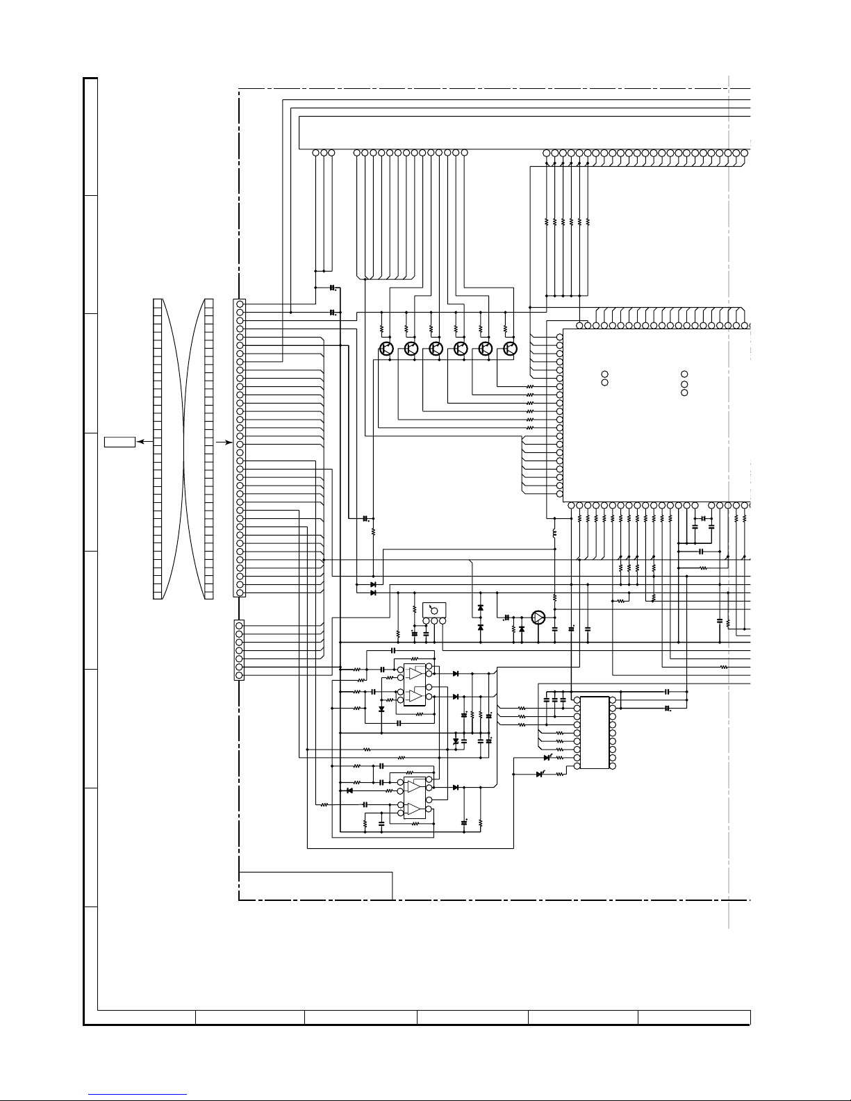
CD-DD4500
– 28 –
Figure 28 SCHEMATIC DIAGRAM (5/14)
A
B
C
D
E
F
G
H
1
23456
• NOTES ON SCHEMATIC DIAGRAM can be found on page 49.
63Hz
10kHz
1kHz
TUN_SM
DI
SP_DET
TUN_FNC
AC_RLY
HP/MIC_IN
DIST_OUT
SMUTE
DD_LP
DD_CS
RESET
CE
DD_ST
DO
DD_LOCK
DD_CLK
VPP
SPAN
CLK
TX
LCK2
F_RLY
DD_ACK
CD_CLK
P_IN
DD_DIO
RX
A_10V
–20dB_ATT
5V_BACK-UP
D_GND
–VF
UNSW_5V
–15V
8V
SWD_5V
D_GND
M_12V
6CH VOL_LATCH
KARAOKE_LATCH
VF1
SPEANA
VF2
1
1 36
2
3
4
5
6
7
8
10
11
12
13
14
15
16
17
18
19
9
20
21
22
23
24
25
26
27
28
29
30
31
32
33
34
35
36
36 1
7
6
4
5
1
2
3
NP
G2G1NP
NP
F1
P14
P15
P16
P17
P18
P19
P20
P21
P22
P23
P24
P25
P13
P12
P11
P10
P9P8P7P6P5P4P3P2P1
G14
G13
G12
G11
G10
G9G8G7G6G5G4G3
F1
F1
80
79 78
77
76
75
74
73
72
71
70
69 68
67
66
65
64
63 62
61
60
5
P23
P24
P22
P25
P21
P20
P9
P10
P12
P17
P16
P19
P15
P14
P13
P8
P18
P7
P11
VDD2
P6
P7P8P9
P10
P11
DIST0/P18
P17
P16
P15
P14
P13
P12
VLOAD
P23
DIST OUT
SPAN/P25
P24
P22
DIST3/P21
DIST2/P20
DIST1/P19
100
99
98
97
96
95
94
93
92
91
90
89
88
87
86
85
84
83
82
81
P4
P5
P6
P3
P2
P1
G8
G7
G6
G5
G4
G3
G2
G1
G12
G13
G14
P1
P2
P3
P4
P5
G11
G10
G9
G8
G7
G6
G5
G4
G3
AVDD
PLAY SW B/FPA/FPB
O_C/DISC_NO_SW
SPEANA1
KEY0
SPEANA3
VSS1
SPEANA2
X1
DRF(4500ONLY)
HEADPHONE/MIC_IN
DVD DI/CD DI
KEY1
DVD_BUSY/CD_CE
DVD_STB/WRQ
DVD_DO/CD_DO
X2
VDD1
VPP/IC
TUN_SM
KEY2
AVSS
KARAOKE_LATCH
L,R 63Hz
L,R 10kHz
TUNER_FUNC/CD_R
E
MOT_SPEED_CNT
G2
G1
L,R 1kHz
1 2 3 4 5 6 7 8 9
10
11 12 13 14 15 16 17 18 19 20 21
2
18
17
16
15
14
13
12
11
10
9
8
7
6
5
4
3
2
1
VSS
DATA
CLOCK
LCK
STOP
F PLAY
CD DISC1
CD DISC2
CD DISC3
R_PLAY
L+
L–
T1_SOL
T2_SOL
OE
__
VDD
T_MOT
DVD_RX
VPP
HP/MIC_IN
TX
RX
KEY0
KEY1
KEY2
SPEANA1
SPEANA2
SPEANA3
TUN_SM
RD68
220K
+VCC
8
7
6
5
4
3
2
1
–
+
+
–
MOT_CNT
8
7
6
5
4
3
2
1
–
+
+
–
P_IN
SPEANA3
LCK1
SPEANA2
DI
CLK
SPEANA1
T_MOT
T1_SOL
T2_SOL
3 2 1
5V USWD
5V BACK UP
100
99
46
45
52
CNP8
DISPLAY PWB-B1
123 6 7 8 9 10 11 12 13 14
15 16 17 18 19
29 30 31 32 33 34 35 36 37 38 39 40 41 42 43 44 45 46 47 48 49 50 51 52 53
+B
+B
+B
+B
+B
+B
+B
+B
+B
+B
+B
+B
+B
+B
+B +B +B
+B
+B
-B
-B
-B
CNP601
TO
MAIN PWB
C713
47/25
CNP701
FFC701
RD69
150K
C756
0.022
RD65
15K
RD38 1K
RD37 1K
FL701
FL DISPLAY
LED701
4204UYT7
D704
DS1SS133
D703
DS1SS133
R765
47K
L701
100µF
CNP704
RD43
1K
RD89 10K
RD88 10K
RD80 100K
RD81 100K
RD82 100K
RD83 100K
RD84 100K
RD85 100K
C715
3.3/50
Q707
KRC102 M
R764
100K
R763
100
RX701
REMOTE
SENSOR
C714
0.022
R762
22K
C702
47/50
C720 47/16
C719 0.022
C721
100P
C722
100P
C723
100P
RD50
1K
IC702
BU2092F
INPUT/OUTPUT EXPANDER
RD41 1K
RD42
1K
LED702
4204UYT7
RD34 1K
RD36 1K
RD35 1K
R792
10K
R793
10K
R783 1K
R761
33
C703
1/50
R784
100K
Q706
KTC3199 GR
RD32
1K
IC701
IX0442AW
SYSTEM MICROCOMPUT
E
C708
0.022
R766
10K
D702
DS1SS133
D701
DS1SS133
R769
10K
R755 1K
R754 1K
R753 1K
R752 1K
R751 1K
R768 10K
R767
10K
C707 0.022
0.022
C706
Q705
KTC3199 GR
Q704
KTC3199 GR
Q703
KTC3199 GR
Q702
KTC3199 GR
Q701
KTC3199 GR
R760
100K
R759
100K
R758
100K
R757
100K
R756
100K
R713 1K
R714 100
R715 100
R704 1K
R712 1K
R710 1K
R711 1K
XL701
C704
15P(CH)
C705
18P(CH)
R709 1K
R708 1K
R707 1K
R706 1K
R705 1K
R703 1K
R702 1K
R701 1K
RD72
100K
C737
2.2/50
RD71 180K
C731
0.022
C732
0.022
C733
47/25
D712
DS1SS133
C718
220/10
RD56
33K
D709
DS1SS133
D710
DS1SS133
ZD701
DZ6.2BSC
C728
2.2/50
RD57
220K
RD58
2.2M
D708
DS1SS133
C724 270P
C725
270P
C726
0.0068
RD55
470K
RD54
22K
RD53
33K
RD62 100K
RD64
68K
C735
0.0027
C736
0.022
RD52 330
RD61 100K
C730 2.2/50
RD59 820K
RD51 100
IC704
KIA4558P
OPE AMP.
RD60 1M
IC703
KIA4558P
OPE AMP.
C727 0.0068
RD70 390K
C734 0.0027
RD63
12K
D711
DS1SS133
C717
0.01
D705
DS1SS133
C701
47/50
2
3
1
Page 29

– 29 –
CD-DD4500
Figure 29 SCHEMATIC DIAGRAM (6/14)
7
8 9 10 11 12
NP
NP
P20
F2F2F2
P21
P22
P23
P24
P25
DIST_OUT
KARA_LAT
VOL_LAT
ATT
F_RLY
SMUTE
AC_RLY
65
64
63 62
61
60
59
58
57
56
55
54 53
52
51
P23
P24
P22
P25
P21
P20
6CH VOL_LATCH
(500/200 ONLY)
SMUTE
AC_RLY_CNT
P23
SP_RLY(FRONT)
T1_RUN
DIST_OUT
SPAN/P25
P24
P22
DIST3/P21
DIST2/P20
TIMER_LED
–20dB_ATT
LCK2
DD_STATUS
DD_DO
DD_CLK
DO
DD_DI
DVD_DI/CD_DI
DVD_CLK/CD_CLK
DVD_BUSY/CD_CE
DVD_DO/CD_DO
P_IN
X2
VDD1
VPP/IC
JOG_0
REMOCON
CE
DD_LP
DD_CS
DD_LOCK
VSS0
VDD0
T2_RUN
CD_CLAMP_SW
LCK1
RESET
CLK
DD_ACK
DI
SP_DET
JOG_1
RAOKE_LATCH
NER_FUNC/CD_RES_OUT
T_SPEED_CNT
17 18 19 20 21 22 23 24 25 26 27 28 29 30
50
49
48
47
46
45
44
43
42
41
40
39
38
37
36
35
34
33
32
31
OC/D1_SW
CLAMP SW
TUN_FNC/RES_OUT
DVD_CLK/CD_CLK
DVD_DI/CD_DI
DVD_DO/CD_DO
DVD_BUSY/CD_CE
DVD_RX/DRF
DVD_STB/WRQ
1 2 3 4 5 6 7 8 9
987654321
987654321
KEY1
KEY0
KEY2
R_REC
T2 PLAY
T2 RUN
+MTR
SOLA/SOLB
T1 RUN
GND
F_REC
4
5
6
3
2
7
8
1
T1_SOL
T_MOT
T2_SOL
A
B
1
2
3
CD_CLK
VPP TXRX
DO
CLK CEDI
P_IN
SP_DET
TUN_FNC
MOT_CNT
DD_CS
DD_LP
RESET
LCK1
DD_ST
DD_LOCK
DD_ACK
LCK2
TIMER
CNP8
TO
CD SERVO PWB
8
1
+
-
M
TAPE MECHANISM
PWB-F
8
7
6
5
4
3
2
1
TAPE
MOTOR
PLAY
F. PLAY
CASSETTE
SOLENOID
SOLENOID
PH
FC702
48 49 50 51 52 53 56 57 58
+B
+B
+B
+B
+B
+B
+B
+B
+B
+B
+B
+B
CNP702
R775
10K
D707
DS1SS133
D706
DS1SS133
R774
4.7K
C712
47/25
Q708
KTA1271 Y
Q709
KTA1271 Y
Q710
KTA1273 Y
R780
10K
R781
10K
R782
10K
RD91
3.3K
RD92 10K
RD93 10K
RD94 10K
BI703
CNS703
R726 100
RD90
3.3K
R727 1K
RD89 10K
10K
RD86 3.3K
RD87 3.3K
C711
0.001
R799 47K
R785 47K
R798 10K
Q712
KRC104 M
R791 47K
LED709
4204S.T7
RD32
1K
01
AW
OCOMPUTER
R773 10K
R772
10K
C709
0.022
C710
0.001
JOG701
JOG VOLUME
C708
0.022
R719 1K
R718 1K
R770
10K
R771
10K
RD17
1K
R790 47K
R789 47K
R788 47K
R787 47K
R786 47K
R725
100
R724 1K
R778
10K
R777
10K
0.022
R736 1K
R735 1K
R734 1K
R733 1K
R741 1K
R740 1K
R739 1K
R738 1K
R737 1K
R732 1K
R731 1K
R730 100
R729 100
R728 1K
R713 1K
R714 100
R715 100
R716 1K
R717 1K
XL701
C705
18P(CH)
R720 1K
R721 1K
R722 1K
R723 1K
RD31
100K
RD08
5.6K
RD03
1K
SW724
TUNING
DOWN
RD11
33K
SW708
DISC 1
RD05
2.2K
RD10
18K
SW707
VIRTUAL
SW729
STOP
SW701
POWER
RD06
2.7K
SW716
EQUALIZER
RD13
680
RD14
820
SW711
DISC
SKIP
RD29
15K
RD26
3.9K
SW727
FAST
FORWARD
RD24
2.2K
SW728
PLAY
SW733
VIDEO
SW732
TUNING
UP
SW734
TUNER
RD27
5.6K
RD30
33K
SW731
REC/PAUSE
RD28
10K
RD25
2.7K
SW723
TAPE
SW726
FAST
REWIND
SW725
MEMORY
SET
RD20
680
SW722
CD
RD22
1K
SW715
X_BASS
RD01
680
SW710
DISC 3
RD02
820
SW709
DISC 2
SW705
NORMAL
RD07
3.9K
SW703
TIMER
SW704
BYPASS
RD04
1.5K
SW702
CLOCK
SW706
PHANTOM
SW714
DIMMER
SW712
OPEN/
CLOSE
RD09
10K
RD21
820
RD23
1.5K
DD_DIO
DD_CLK
R743 1K
R744 1K
R750 1K
R749 1K
R748 1K
R747 1K
R746 1K
R745 1K
Page 30

CD-DD4500
– 30 –
Figure 30 SCHEMATIC DIAGRAM (7/14)
A
B
C
D
E
F
G
H
1
23456
• NOTES ON SCHEMATIC DIAGRAM can be found on page 49.
+B(18V)
TRANSFORMER
PWB-D3
3
1
2
P_IN
–B2
GND
+B2
+18V
GND
ASSIST
GND
–VF
VF2
VF1
+B(+9V)
D_GND
AT5V
AC_RLY
+B2
–B2
GND
–B1
+B1
P_IN
+18V
GND
–VF
VF2
VF1
+9V
AC_RLY
AT5V
D_GND
5
132
4
5
132
4
5
132
4
152
43
8
7
6
152
43
8
7
6
4
5
27
6
1
3
89
10 11 12
CNP801
TO
AMP. A PWB
P35 11-F
CNS850
FROM
MAIN PWB
P27 12-G
POWER PWB-D1
+B
+B
+B
+B
+B
+B
-B
+B
+B
-B
+B
+B
+B
+B
+B
-B -B
AC POWER
SUPPLY CORD
AC 120 V
60 Hz
+B
BI801
CNS801
CNP807
D811
1N4004S
R816
47K
R817
12K
C814
100/35
DZ804
DZ6.2BSA
R815
10
C812
47/50
C813
47/50
DZ803
DZ36BSC
C811
100/50
C816
100/50
D810
1N4004S
D808
1N4004S
D809
1N4004S
C815
100/50
C808
100/50
D807
1N4004S
D803
D803~D806 :
1N4004S
D806
D804
D805
C805
0.047(ML)
C806
0.047(ML)
C810
100/63
D802
TS6B04GM
C804
0.047
(ML)
C803
0.047
(ML)
C802
0.047
(ML)
C801
0.047
(ML)
D801
TS6B04GM
T.F.
T801
POWER
TRANSFORMER
C880
0.0047
D880
DS1SS133
L802
LINE FILTER
F801
6.3A/125V
C881
0.047(ML)
D884
1N4004S
C882
470/35
D883
1N4004S
D882
1N4004S
D881
1N4004S
IC880
KIA7805AP
CONSTANT
VOLTAGE
REGULATOR
D885
DS1SS133
C883
1000/6.3
DZ802
DZ2.4BSB
R812
47K
R813
220K
Q880
KTC3199 GR
R882
47K
C884
0.047(ML)
C885
100/16
BI802
CNS802
CNP802
T802
SUB
TRANSFORMER
RY801
R822
56(1/2W)
R821
56(1/2W)
R883
100
R814
2.2K
Q806
KTA1274 Y
R819
47
R818
47
C809
100/50
F803
4A /125V
F804
6.3A/125V
F805
6.3A /125V
F806
2A/125V
F807
2A/125V
F802
4A /125V
Page 31

– 31 –
CD-DD4500
Figure 31 SCHEMATIC DIAGRAM (8/14)
7
8 9 10 11 12
(20W x 2)( 30W )
CENTER & SURROUND
A_GND
C-CH
RS-CH
SR_RLY
C_RLY
LS-CH
264153
M_12V
FAN_CTL
FAN_SIG
20ATT
SP_DET
SMUTE
265413
265413
FAN_SIG
FAN_CTL
SP_DET
19
18
17
16
15
14
13
12
11
10
9
8
7
6
5
4
3
2
1
+
C-CH
–
+
RS-CH
–
–
LS-CH
+
21
21
12
M
M
21
C_RLY
SR_RLY
FAN_SIG
SURROUND
SPEAKER R-ch
SURROUND
SPEAKER L-ch
CENTER
SPEAKER
GND
–B1
GND
+B1
4321
4321
CNP902
TO
AMP. A PWB
P34 1-F
265413
CNP603
TO
MAIN PWB
P27 12-C
AMP. B PWB-J
CNP904
TO
AMP. A PWB
P35 11-G
FM SIGNAL
IC401
STK40224
2
1
3
+ +
C462
0.027
(ML)
C431
10/50
C430
10/50
BI403
CNS403
C461
2.2/50
R409
1K
C460
2.2/50
R410
1K
R437
1K
Q403
2SC2878 B
Q401
2SC2878 B
Q404
2SC2878 B
Q408
2SC2878 B
Q402
2SC2878 B
R484
10(1/2W)
R476
10(1/2W)
R480
3.9K
R479
1K
D410
DS1SS133
R486
330(1/2W)
C444 470P
C442 470P
C402
0.001
C401
0.001
C403
0.001
C404
0.001
R481
56K
R483 56K
R482 56K
C426 15P
R440
56K
R411
820
R412
820
R438
820
C425
2.2/50
C406
47/50
C405
47/50
R407
2.2K
R408
2.2K
R436
2.2K
C424
0.001
C443 470P
C423
0.001
R401
2.2K
R402
2.2K
R433
2.2K
R403
8.2K
R404 8.2K
R434 8.2K
R435
1K
R405
1K
Q407
2SC2878 B
R406
1K
CNP402
CNP401
C458
47/16
R478
330(1/2W)
Q421
KTA1271 Y
R471
22K
DZ403
DZ3.9BSB
Q423
KTC3199 GR
R472
1K
D409
DS1SS133
Q420
KRC107 M
R473
220K
Q422
KTC3203 Y
C456
10/50
R477
470K
C455
100/10
DZ404
DZ5.6BSB
Q424
2SB1565 F
C457
47/50
R443
100
R442
100
C427
560P
C409
560P
IC401
STK40224
POWER
AMP.
C410
560P
C428
0.22/50
C432
100/50
R441
22K
L403
Z0137
C433
0.022
L401
Z0137
L402
Z0137
R446
1K
Q409
KTC3199 GR
R444
10K
R424 56K
R445
0.1(1W)
R450 56K
R423 56K
R426 4.7
C437 0.1(ML)
R451 4.7
C414 0.1(ML)
R425 4.7
C413 0.1(ML)
R454
47K
Q412
KTC3199 GR
R453
1K
R455
47K
R452
1K
Q413
KTC3199 GR
D406
DS1SS133
D405
DS1SS133
RY402
RY401
R427
4.7K
R456
4.7K
R428
4.7K
R449 56K
BI407
Q411
KTC3199 GR
C435 47/50
D404
DS1SS133
D401
DS1SS133
Q410
KTC3199 GR
R421
1K
R417
10K
D402
DS1SS133
R419
0.1(1W)
C411
0.022
Q405
KTC3199 GR
R418
10K
Q406
KTC3199 GR
R422
1K
R420
0.1(1W)
C412
0.022
D403
DS1SS133
R416
56K
C408 15P
C407
15P
R414
1K
R415
56K
R413
1K
R439
1K
SOC401
SPEAKER JACK
C429
100/50
BI406
CNS406
CNS407
SP_DET
CNS402
M402
FAN MOTER
M401
FAN MOTER
CNS401
Page 32

CD-DD4500
– 32 –
Figure 32 SCHEMATIC DIAGRAM (9/14)
A
B
C
D
E
F
G
H
1
23456
• NOTES ON SCHEMATIC DIAGRAM can be found on page 49.
DOLBY PWB-H
FM SIGNAL
DIGITAL
OUT
DGND
2
1
2
1
BI7
CNS7
VDDX
XI
XO
VSSX
SCKI
VSSDL
SCKO
DLCKS
DLON
LPFO
VDDDL
PO7
PO6
PO5
PO4
PO3
STATUS
PO1
RSTO
VSS
AD15
AD14
AD13
AD12
AD11
AD10
AD9
AD8
VDD
AD7
AD6
AD5
AD4
AD3
AD2
AD1
AD0
VSS
IO0
IO1
IO2
IO3
IO4
IO5
IO6
IO7
VDD
CE
OE
WR
VSS
LOCK
CKO
VSSA
CKI
AMPO
AMPI
PLON
VDDA
PDO
TSTSUB2
TSTSUB1
FCONT
TSTSUB0
VSS
RX
TEST3
TEST2
TXO
BCKOB
LRCKOB
TEST1
TEST0
BCKOA
LRCKOA
VDD
SDI1
SDI0
BCKB
LRCKB
SDO3
SDO2
SDO1
SDO0
BCKA
LRCKA
VSS
IRQ
FI3
FI2
FI1
FI0
MIACK
MICK
MIDIO
MILP
MICS
MIMD
RST
515266 65 64 63 62 61 60 59 58 57 56 55 54 5380 79 78 77 76 75 74 73 72 71 70 69 68 67
100
99
98
97
96
95
94
93
92
91
90
89
88
87
86
85
84
83
82
81
1
1
3
2
1
3
2
234
5
6
7
8
9
10 11 12 13 14 15 16 17 18 19
20
21
22
232425
26
27
28
29
30
50
49
48
47
46
45
44
43
42
41
40
39
38
37
36
35
34
33
32
31
3
2
1
OUT
GND
+B
2
1
14
13 12
11
10
98
1234567
GND
VCC
100
99
30
2
1
1
3
BI
5
AD16
FROM
CD SERVO
PWB
P25 12-E
+B
+B
+B
+B
+B
+B
+B
+B
+B
+B
+B
+B
+B
+B
R519
2.2K
C500 0.1
C501 10/16
C7013
0.022
IC501
TORX178B
L500
10µH
CX02
0.022
D509
1SS133
D508
1SS133
CX03 0.022
D506
1SS133
D507 1SS133
C523 0.01
C524
0.47
C577
0.022
L511
100mA
L510
100mA
L507
100mA
L506
100mA
L505
100mA
L512
100mA
C7014
0.001
L513
100mA
IC502
74VHC00F
INVERTOR
Q505
KRC104 M
R516
18K
R521
1K
CNP501
C503 0.1
D501 1SS133
C507 10/16
C512 0.1
D500
1SS133
C526 10/
1
C525
0.1
R512
15K
C527
100P
(CH)
R
5
1
0
R510
1K(F)
R509
1K(F)
R511
10K
C520
10/16
C519
0.1
R
5
4.
C517
0.1
R502
1K
R503
1K
R504 1K
R505 100
R506 1K
C511
10/16
C513
0.1
X501
2.2MHz
R500
2.2M
C506
10P
(CH)
C505
15P
(CH)
C599
0.0047
R501
1K
C515
0.1
C514
0.1
C504
10/16
C508
0.1
C518
470/10
R508
1K
IC504
IX0443AW
DOLBY DECODER
Q503
KRC104 M
L501
0.82µH
Page 33

– 33 –
CD-DD4500
Figure 33 SCHEMATIC DIAGRAM (10/14)
7
8 9 10 11 12
44
43
42
41
40
39
38
37
36
35
34
34
22
20
19
18
17
16
15
14
13
12
123456 879
10 11
33 32 31 30 29 28 27 26 25 24 23
PDN
LOOP0
DIF1
DIF0
P/S
MCLK
DZF1
AVSS
AVDD
VREFH
VCOM
DZF2
RIN–
RIN+
LIN+
LIN–
ROUT3
LOUT1
LOUT2
LOUT3
22
21
CAD0
CAD1
ADIF
NC
TST
DVSS
DVDD
TVDD
DZFE
NC
DFS
DAUX
SDTO
SDTI3
SDTI2
SDTI1
LRCK
BICK
SMUTE
I2C
SDOS
44
21
LOOP1
ROUT2
ROUT1
RF
AGND
LF
AGND
SW
AGND
CENTER
AGND
RS
AGND
LS
AGND
RO
AGND
LO
2
3
4
5
6
7
8
9
10
11
12
13
14
15
1
FFC607
TO
MAIN PWB
P27 7-A
STATUS
LOCK
RESET
DDLAT
DDAC
DIO
CK
DDCE
A10V
D5V
DGND
2
3
4
5
6
7
8
9
10
11
12
1
2
1
1
2
1
3
BI501A
BI501B
2
CNP607
FFC602
TO
MAIN PWB
P26 5-A
CNP602
12 1
15 1
112
115
+B
+B
+B
+B
+B
+B
+B+B
+B
+B
+B
+B
+B
+B
+B
C523 0.01
C524
0.47
R513
100
C578
0.022
C579
0.022
C7015
0.022
D512
1SS133
D513
1SS133
C7016
0.022
D502
1SS133
D503
1SS133
CX04
0.022
D510
1SS133
D511
1SS133
C538
0.001
C577
0.022
Q520
KRC104 M
L570
0.82µH
R574
4.7K
C554
0.1
C552
10/16
R538
4.7K
Q572
2SD468-C
C576
0.022
R578
390
R577
390
C574
47/25
DZ571
MTZJ5.6A
C575
100/10
C573
100/10
C571
47/16
IC571
TA48M033F(S)
3.3 V VOLTAGE REGULATOR
21
C555
0.1
R573
4.7K
R537
4.7K
C553
10/16
CNP503
CNP502
C526 10/16
C525
0.1
R512
15K
C527
100P
(CH)
R514
10K
R510
1K(F)
C528 120P(CH)
R509
1K(F)
R511
10K
R515
4.7K
C540 10/16
C541 10/16
C542 10/16
C543 10/16
C544 10/16
C556
0.001
C531
0.1
R556
470
C533
0.1
IC505
AK4527BVQ
6-CH
CODEC IC
R559 470
C530
10/16
C545 10/16
C557
0.001
R557 470
R558 470
C532
2.2/50
C535
0.01
C536
0.1
C537
10/16
R540
10K
R541
10K
R531
1K
R530
1K
R549 27K
R550 27K
R551 27K
R552 27K
R553 27K
R554 27K
R536
100K
R535
100K
C546 0.015
C547 0.015
C548 0.015
C549 0.015
C550 0.015
C551
0.015
C558 4.7/25
C559 4.7/25
R544 220
R545 220
R546 220
R547 220
R548 220
R543 220
R542
10K
3
R532
10K
Page 34

CD-DD4500
– 34 –
Figure 34 SCHEMATIC DIAGRAM (11/14)
A
B
C
D
E
F
G
H
1
23456
• NOTES ON SCHEMATIC DIAGRAM can be found on page 49.
M
(30
W
S
(40
W
SP_DET
SMUTE
FAN_CTL
FAN_CTL
F_RLY
SW_RLY
H/P
FAN_SIG
SMUTE
M_12V
FAN_SIG
20ATT
CNS406
FROM
AMP. B PWB
P31 9-H
SP_DET
SMUTE
20ATT
SMUTE
2/6_SEL
SW_MUTE
A_GND
S.W.
A_+10V
M_12V
SP_DET
+5V
M_GND
A_–13V
GND
FL-CH
FR-CH
15
14
13
5
3
2
1
15
14
13
5
3
2
1
9
10
11
12
13
14
15
16
17
18
19
8
7
6
5
4
3
2
1
11
10
9
8
7
6
5
4
3
2
1
12
13
14
15
16
17
18
19
8
7
6
5
4
3
2
1
16
15
14
13
12
11
10
9
8
7
6
5
4
3
2
1
16
15
14
13
12
11
10
9
876
5
4
3
2
1
1
6
5
4
3
2
8
7
6
5
4
3
2
1
–
+
–
+
+
+
–
–
–
+
–
++
–
+
–
IC904
KIA4558P
IC905
TC4053BP
+B
+B
+B
+B
+B
+B
+B
-B
-B
-B
+B
+B
+B
+B
+B
22
2
2
1
3
1
3
1
1
3
3
FROM
MAIN PWB
P27 12-D
AMP. A PWB-D2
FM SIGNAL
C903
0.022
R905
4.7K
R901
18K
R902
18K
R906
4.7K
R904
18K
C906
0.022
C907
100P
R907
8.2K
R908
8.2K
C908
100P
R910
1.5K
R909
1.5K
C967
0.022
C966
47/50
C910
10/16
C909
10/16
IC904
KIA4558P
OPE AMP.
R916
1K
R919
68K
R920
68K
C916
0.1(ML)
C914
2.2/50
R913
1K
C969
47/25
C968
0.022
(ML)
C915
0.1(ML)
R1003
390
C912
0.015(ML)
R1000
330
R912
100K
R911
100K
C911
0.015(ML)
R1002
1.2K
R1001
100
DZ901
DZ5.1BSB
R1004
56K
DZ902
DZ5.1BSB
R918
68K
R917
68K
C917
220P
(CH)
C918
220P
(CH)
R1006
100
C972
2.2/50
C973
0.022
R1042
100K
R1055
10K
R1008
1K
R1007
1K
R1010
10K
R922
8.2K
C1012
2.2/50
R1056
5.6K
R1041
100K
R1009
10K
C971
2.2/50
IC907
KIA4558P
OPE AMP.
R1011
2.2K
C1014
10/50
R1012
1K
R940
820
C930
47/50
R934
2.2K
C924
0.001
C1013
2.2/50
R921
8.2K
R935
2.2K
C925
0.001
Q907
2SC2878 B
R1053 220K
C1009
470P
C977
0.22/50
R1014
22K
C997
2.2/50
R1049
56K
R1048
56K
R951
1K
C937
220P
R939
1K
C929
47/50
R943
56K
C931
15P
R950
56K
R944
1K
C998
2.2/50
R1052
220K
I
C
ST
K
PO
W
C979
100/50
C
9
10
C982
10/50
C978
100/50
C
9
1
0
C980
10/50
R1013
22K
C976
0.22/50
C999
2.2/50
R948
1K
R938
820
C928
47/50
R1046
56K
R1050
220K
Q917
2SC2878 B
R1054
220K
C974
0.001
C926
0.001
R936
2.2K
R928
8.2K
C1010
2.2/50
S
T
PO
W
C936
220P
R946
56K
C932
15P
R949
1K
C1001
2.2/50
R937
820
C927
47/50
R1047
56K
C935
220P
R947
56K
R941
1K
C933
15P
R1051
220K
C1007
470P
Q905
2SC2878 B
R933
2.2K
R927
8.2K
C1011
2.2/50
C923
0.001
R1043
100K
R1044
100K
IC906
TC4053BP
R1005
1K
C1008
470P
Q916
KRA107 M
C965
3.3/25
C964
1/50
C1015
3.3/25
Q914
KRA107 M
Q913
KRA107 M
C963
1/50
R997
22K
R998
22K
CNP902
CNP901
CNS604
R903
18K
C905
0.082
(ML)
C904
0.082(ML)
C902
0.15
C901
0.15
Q915
KRC107 M
C913
2.2/50
Q908
2SC2878 B
Q906
2SC2878 B
R945
820
C934
15P
C1006
470P
C938
220P
R952
1K
R942
1K
IC905,IC906
TC4053BP
TRIPLE 2CH
MULTIPLULEXER
Page 35

– 35 –
CD-DD4500
Figure 35 SCHEMATIC DIAGRAM (12/14)
7
8 9 10 11 12
MAIN
(30W x 2)
SUB
(40W x 2)
HEADPHONES
PWB-B2
H/P_SW
R-CH
A_GND
L-CH
4
1
4
4
1
1
2
3
SW_RLY
H/P
SP_DET
F_RLY
FAN_SIG
GND
GND
–B2
+B2
+B
+B
+B
+B
+B
-B
-B
-B
-B
-B
-B
R-CH
L-CH
GND
–B1
+B1
+B1
–B1
GND
–B2
+B2
L-CH
R-CH
SP_SWL-CH_GND
SP_SWL-CH
SP_SWR-CH_GND
SP_SWR-CH
SP_FR-CH_GND
SP_FL-CH
SP_FL-CH_GND
SP_FR-CH
FRONT
SPEAKER
R-CH
FRONT
SPEAKER
L-CH
SUBWOOFER
L-CH
SUBWOOFER
R-CH
13
12
11
10
9
8
7
6
5
4
13
12
11
10
9
8
7
6
5
4
6
7
8
1
2
3
4
3
4
5
1
2
8
7
6
5
4
3
2
1
R-CH
–
+
–
L-CH
+ +
–
R-CH
+
–
L-CH
+B
+B
+B
+B
+B
+B
-B
CNS403
FROM
AMP. B PWB
P31 9-A
CNS801
FROM
POWER PWB
P30 2-H
R1014
22K
220P
IC901
STK40270N
POWER AMP.
R972
1K
C942
0.022
C941
0.022
R967
10K
D903
DS1SS133
Q911
KTC3199 GR
C985
100/50
R1018
100
R1016
100
C979
100/50
C983
10/50
C982
10/50
Q937
KTA1046 Y
R1045
1.5K
C991
0.022
C990
100/16
C1003
47/25
R1031
100
RP901
2.2 ohms
C987
3300/50
C986
3300/50
R1022
22K
C995
4700/50
R1040
22K
R1039
22K
C996
4700/50
R1023
22K
R1025
47K
R1020
1K
Q921
KTC3199 GR
R977
4.7
R980
4.7
C943
0.1(ML)
C946
0.1(ML)
R1024
56K
C988
330/6.3
D905
DS1SS133
Q919
KTC3199 GR
Q918
KTC3199 GR
R976
56K
R975
56K
Q920
KTC3199 GR
C945
0.1(ML)
R978
4.7
R979
4.7
C944
0.1(ML)
R974
56K
R973
56K
RY902
R987
330(1/2W)
R988
330(1/2W)
D906
DS1SS133
FW901
R1034
10K
C993
0.01(ML)
R994
4.7K
R989
4.7K
R990
4.7K
R1032
220
R991
4.7K
RY901
D908
DS1SS133
L904 0.29µH
L903 0.29µH
L901
0.29µH
L902
0.29µH
CNP904
D901
DS1SS133
R970
1K
C940
0.022
R964
10K
D902
DS1SS133
Q910
KTC3199 GR
C939
0.022
R963
10K
R969
1K
Q909
KTC3199 GR
R962
0.1(1W)
R961
0.1(1W)
R1017
100
C984
100/50
R1015
100
C978
100/50
C981
10/50
C980
10/50
R1013
22K
IC902
STK40270N
POWRW AMP.
R971
1K
R966
0.1
(1W)
0
D904
DS1SS133
R968
10K
Q912
KTC3199 GR
R965
0.1(1W)
DZ903
DZ13BSC
R10191KR1021
47K
CNP801
SO901
SPEAKER
TERMINAL
LUG901
SOC901
SUBWOOFER
PRE OUT
JACK
R742
22K
JK701
HEADPHONES
CNP703
L702
2.2µH
Page 36

CD-DD4500
– 36 –
Figure 36 SCHEMATIC DIAGRAM (13/14)
A
B
C
D
E
F
G
H
1
23456
• NOTES ON SCHEMATIC DIAGRAM can be found on page 49.
1
3
2
AM
LOOP
ANTENNA
FM
2
3
1
123
2
21222324
FM IF IN
AM MIX OUT
AM OSC OUT
FM AFC
AM OSC IN
AM RF IN
VSM
REG
2
1
3
TP301
1234
5
6
1
1819202122
NC
X OUT
X INCEDICLDO
VDD
PD
AIN
AOUT
VSS
CLK
DICEDO
AM ANT.
+B
+B
+B
+B
+B
4.5 V
0
4.6 V
C336
0.001
VR351
10K(B)
R386
1K
C342
0.022
L353
1mH
C310
100P
(CH)
C311
100P
(CH)
C312
100P
(CH)
C384
0.001
R372
1K
R373
1K
R374
1K
D305
DS1SS133
D306
DS1SS133
C339
100P(CH)
R323
68K
C334
15P(UJ)
C337
0.022
VD301
SVC348S
T306
AM OSC.
C335
330P
C332
0.022
C331
0.047
R358
8.2K
C343
33P(CH)
C389
0.001
Q371
KTA1266 GR
R384
R371
4.7K
IC302
LC72131
PLL(TUNER)
C390
0.001
C394
47/25
R380
1.5K
R379
2.2K
C392
0.001
C393
1/50
R381
10K
R345
4.7K
C321
100/16
C323
0.022
T302
AM TRACKING
T351
AM I
F
C341
0.022
C346
0.022
R301
150
CF302
L342
2.2µH
X352
4.5 MHz
C381
12P(CH)
C382
15P(CH)
C397
0.022
R336
10K
C330
12P(UJ)
D304
DS1SS133
D301
DS1SS133
D302
DS1SS133
CNP301
C338
0.001
C352
10/16
C351
0.022
R351
5.6K
C361
0.022
C362
3.3/50
R382
150
C380
10/16
C347
0.022
D303
DS1SS133
C301
0.001
R369
470
C345
0.022
C350
0.047
8
7
6
5
43 21
ANT
GND
GND
GND
VT
VCC
IF OUT
F OUT
FE301
FM FRONTEND
AM BAND
COVERAGE fL
FM MUTE
LEVEL
Page 37

– 37 –
CD-DD4500
Figure 37 SCHEMATIC DIAGRAM (14/14)
7
8 9 10 11 12
2
1
3
314265789
10
TO
MAIN PWB P26 1-D
MAIN PWB-A (2/2)
FM SIGNAL
AM SIGNAL
123
4
5
6
7
8
9
10 11 12
131415161718192021222324
FM IF IN
AM MIX OUT
AM OSC OUT
FM AFC
AM OSC IN
AM RF IN
AM LOW CUT
VSM
FM/AM OUT
MPX VCO
MPX IN
R-CH OUT
L-CH OUT
PHASE
(FM/AM)
PHASE
IF OUT
VCC
FM DET
STEREO
SD
GND
AM IF IN
REG
MO/ST
TP302
A_+10V
TUN_R
TUN_L
D_GND
TUN_SM
A_GND
CE
CLK
DI
DO
1234
5
6
7
8
9
10 11
1213141516171819202122
NC
MUTE
IO2
IF IN
X OUT
X INCEDI
CL
DO
AM IN
FM IN
VDD
PD
AIN
AOUT
VSS
FM
MW
MO/ST
ST IND
NC
CLK
DICEDO
+B
+B
+B
+B
+B
+B
4.5 V
0 V
4.6 V
10 V
9.9 V
9.3 V
VR351
10K(B)
R386
1K
C342
0.022
L353
1mH
C376
0.022
C377
0.047
C310
100P
(CH)
C311
100P
(CH)
C312
100P
(CH)
C384
0.001
R372
1K
R373
1K
R374
1K
R399
10K
CF352
R370
1K
R391
390
R362
1.8K
R361
1.8K
C372
1/50
C371
1/50
R364
2.7K
R363
2.7K
C373 0.033
R357
470K
C374 0.033
R358
8.2K
C343
33P(CH)
R354
3.9K
L352
100µH
R389
3.9K
R392
390
ZD351
DZ5.1BSB
C395
0.022
C396
100/10
R383
5.6K
Q371
KTA1266 GR
Q360
KTA1266 GR
R384
5.6K
R371
4.7K
C391
47/25
R385
5.6K
D352
DS1SS133
C370
1/50
R377
47K
L351
100µH
R393
1K
C394
47/25
C387
0.022
R380
1.5K
R379
2.2K
C385
0.01
C392
0.001
C393
1/50
R381
10K
R376
1K
C386
330P
R352
1K
T351
AM IF
C358
1/50
CF351
X352
4.5 MHz
C381
12P(CH)
C382
15P(CH)
R356
1K
C368
1/50
R378
82K
C397
0.022
C366
0.001
R353
270
C354
0.022
C353
0.022
C355
22P
(CH)
C399
0.022
C398
100/10
C356
0.001
C357
2.2/50
R360
4.7K
C352
10/16
C351
0.022
R355
3.3K
IC303
LA1832S
FM IF DET./
FM MPX./AM IF
R351
5.6K
C361
0.022
C362
3.3/50
C364
10/16
C363
0.022
C365
0.022
C367
1/50
R350
2.7K
X351
456 kHz
R359
1.8K
R382
150
C380
10/16
R395
47K
C350
0.047
FM MUTE
LEVEL
Page 38

CD-DD4500
– 38 –
Figure 38 WIRING SIDE OF P.W.BOARD (1/10)
A
B
C
D
E
F
G
H
1
23456
R660
R659
R656
C660
R655
R654
R653
1
4
5
8
C664
C663
R658
R657
R662
C659
R661
R652
R651
R694
R693
R690
C688
R689
R688
R687
1
1
4
4
5
5
8
8
C692
IC607
C691
R692
R691
R696
C687
R695
R686
R685
R672
R680
R679
R676
C674
R673
R675
R674
C677
R678
IC606
C678
R671
R650
R649
R682
C673
R677
R637
R681
R639
R684
R683
R664 R663
C892
C699
R698
R697
1234 5678 9101
1918 1716151413121110
9
R892
C893
R894
C891
R891
R893
R897
R861
R890
R642
R665
C641
R643
C642
C643
R666
R667
C644
R638
R668
R640
C198
R632
C197
121
22 42
25 30 35 40
5101520
C196
R636
R631
C199
R635
C602
C603
C604
R605
R606
C605
C606
C607
C608
C610
C609
C629
R625
C630
R626
C600
C347
C341
C332
C335
C339
R323
C337
C363
R358
C343
R350
R351
C351
R645
C354
C361
C366
R646
R353
C399
R356
R355
C187
C190
C189
C395
R354
C356
C355
C376
R352
C353
R360
C342
R384
R385
R383
R395
R376
R377
R359
R399
R389
1
12345678
23456789
1011
222120 1918171615141312
123456789
101112
242322 212019181716151413
C386
C345
R345
R380
R379
R371
C346
C312
R372
R378
R373
C390
R381
C311
C387
R374
C392
C397
C310
C381
C382
IC605
IC602
131415 161718192021222324
121110
987654321
BCE
BCE
E
ECB
B
C
E
E
C
B
E
C
B
CB
321
12345
6
3
2
1
1
2
3
1
36
1
12
12
1
C666
C658
C662
C665
C661
C657
C690
C694
C686
C693
C689
C685
C676
C680
C672
C675
C679
C681
C671
C682
C668
C667
C696
C695
C684
C698
R896
Q892
Q893
Q891
R895
C862
Q859
CNS
CNP901
R862
R
R
R
R634
CNP603
R641
C648
C647
Q601
ZD602
R633
ZD601
Q602
C649
C650
R644
C633
D185
C683
D186
C646
C188
C638
C645
C640
C634
C639
C654
C637
C653
C636
C632
C195
C194
C631
C655
C635
C656
R601
C626
C601
C625
C623
C612
C611
IC601
C613
C618
C615
C619
C620
R627
R628
D602
D601
CNP502
FFC602
CNP301
D305
D306
D302
D301
C616
C617
C321
C323
L342
C614
T302
C624
C330
C331
VD301
R348
C334
R602
R336
R603
L353
T306
C362
C364
CF302
C365
C352
C367
CNP602
IC303
C357
R357
X351
C368
R364
R362
C370
C372
ZD351
R361
C371
C374
C373
R363
C396
R370
R607
D183
D184
C699
CNP503
TO
DOLBY PWB
P44 1-E
C
FFC607
R604
R392
R391
C358
C377
C398
CF351
L352
CF352
T351
C350
R386
VR351
D352
Q360
C391
R382
C384
C385
R393
R301
Q371
C393
L351
FE301
IC302
C380
R369
C394
X352
C389
D304
C336
D303
C338
C301
1
115
151
2
3
1
7
911
6
8
1012
35791
1
246810
135791113
2 4 6 8 10 12 14
15
JK601
VIDEO/AUX INPUT
R-CH
L-CH
AM LOOP
ANTENNA
TO
DOLBY PWB
P44 6-G
FM
ANTENNA
1
2
3
MAIN PWB-A
BR
COLOR TABLE
RD(R)
OR
YL
GR
BL
VL
GY
WH(W)
BK
PK
BROWN
RED
ORANGE
YELLOW
GREEN
BLUE
VIOLET
GRAY
WHITE
BLACK
PINK
TO
AMP.A PWB
P43 12-E
Page 39

– 39 –
CD-DD4500
Figure 39 WIRING SIDE OF P.W.BOARD (2/10)
7
8 9 10 11 12
1 2 3 4 5 6 7 8 9 10111213141516171819
1918 1716151413121110 9 8 7 6 5 4 3 2 1
R892
C893
R894
C891
R891
R893
R897
R861
R890
R192
R860
1
12
R133
R171
R172
1
18
9
5
15
10
R188
R187
R175
R174
C183
R186
C182
R179
R173
R193
C181
R642
R665
C641
R643
C642
C643
R355
C187
C190
C189
R180
R196
R194
C184
R191
R190
R177
R178
R189
R176
R139
R141
C186
C131
R125
R131
R145
R123
C119
R121
C111
R119
C102
R164
R105
R167
R107
R166
R114
R110
C106
C108
R106
R103
C107
C101
R120
123456789
R113
R101
R117
C112
R122
C114
C113
R104
C127
R142
C120
R124
R134
R111
R146
C139
C140
R140
R126
R132
C132
R153
R154
R136
R135
R108
R109
C395
R354
123456789101112
1211 10 9 8 7 6 5 4 3 2 1
R171
E
E
ECB
B
C
E
E
C
B
E
C
B
CB
C
B
321
12345
6
1
2
3
1
2
3
RDWHGYWHGYWHGYWHGYWHGY
WH
1
36
1
12
36
1
P47 11-E
FROM
TAPE 2
RECORD/
PLAYBACK
ERASE HEAD
FROM
TAPE 1
PLAYBACK
HEAD
P47 10-F
IC181
C698
Q892
Q893
Q891
R895
C862
Q859
CNS604
P901
R862
D855
Q851
C852
C877
D860
D859
BI850
CNS850
TO
POWER PWB
P42 3-H
CNP807
R855
C859
C858
IC851
RP851
C109
C851
C185
R181
R182
R183
R184
R185
R634
CNP603
R641
C648
C647
Q601
ZD602
R633
ZD601
Q602
C649
C650
R644
C633
683
8
362
C370
C372
ZD351
R361
C371
C374
C373
R363
C396
R370
R607
D183
D184
R195
C627
R137
D853
C133
C135
Q103
R858
R857
C128
D181
D182
D852
R856
C121
C123
D851
C117
C860
C856
R854
C857
R850
C854
C853
R853
Q124
R162
Q126
1
2
3
3
1
2
CNP101
Q850
IC850
L103
L104
C152
C151
ZD850
C855
R852
R160
Q128
R168
Q101
C154
C150
IC102
C105
1234567
CNP102
C103
R118
R102
C116
Q102
C115
C118
IC101
C136
C142
C122
C141
C124
C134
R138
C145
C146
R158
Q121
D604
Q122
C699
R157
R156
CNP601
CNP701
TO
DISPLAY PWB
P41 11-A
FFC701
CNP607
R604
R392
R391
8
BI606
CNS606
TO
CD SERVO PWB
P46 5-A
CNP7
131415 161718192021222324
121110
987654321
E
E
C
B
B
E
C
B
B
BCE
BCE
CE
321
123
CE
C
B
1
1
1
3
357
911
2468
1012
3 5 7 9 11 13 15 17 19 21 23 25 27 29 31 33 35
2 4 6 8 1012141618202224262830323436
TO
.A PWB
12-E
CNS407
TO
AMP.B PWB
P45 7-E
RD
GY
WH
Page 40

CD-DD4500
– 40 –
Figure 40 WIRING SIDE OF P.W.BOARD (3/10)
A
B
C
D
E
F
G
H
1
23456
R781
R780
R782
RD09
RD11
RD08
C725
C724
RD59
1
2
3
4
8
7
6
5
1
2
3
4
321
5
6
7
8
RD62
RD53
C732
C734
C735
RD68
RD64
RD70
RD63
RD73
RD71
C731
C756
C736
C711
C719
1
1357
2468
5
910
18
15
R792
IC702
C710
C722
C721
C723
RD35
C707
R711
R712
C704
1
10
0
RD88
R707
R706
R705
R704
R701
C706
R766
C714
1
2
3
4
5
6
7
CNP704
R784
R760
R759
R758
R757
R756
912345678
198765432
SW716
EQUALIZ
E
D706
Q709
RD37
Q708
D707
Q710
RD38
RD14
RD41
C712
R775
JOG701
CNP702
FFC702
P47 9-A
TO
TAPE MECHANISM
PWB
R774
SW715
X-BASS
RD13
SW711
DISC SKIP
RD10
SW710
DISC 3
SW709
DISC 2
SW708
DISC 1
SW712
OPEN/CLOSE
RD07
C733
D710
RD57
D712
C737
RD72
D711
IC703
RD54
RD56
RD58
RD60
C727
C726
IC704
D708
RD55
RD52
ZD701
RD65
RD51
C720
RD34
RD43
RD42
SW707
VIRTUAL
RD36
SW733
VIDEO
RD06
P
H
X
R
R
R
R708
R703
R702
R710
R709
R769
R754
R753
R752
R755
R751
R783
R767
Q701
Q702
Q703
Q706
Q704
Q705
R720
R761
RD32
RX701
BI703
CNS703
TO
CD SERVO
PWB
P46 3-A
CNP8
R763
RD61
C713
R762
C728
C730
D709
R768
RD89
GY
WH
WHGYWHGYWHGYRD
C703
9
ECB
ECB
ECB
ECB
ECB
B
C
E
1
1
2 3 6 7 8 9 10111213141516171819
20
B
C
E
B
C
E
B
C
E
BR
COLOR TABLE
RD(R)
OR
YL
GR
BL
VL
GY
WH(W)
BK
PK
BROWN
RED
ORANGE
YELLOW
GREEN
BLUE
VIOLET
GRAY
WHITE
BLACK
PINK
DISPLAY PWB-B1
Page 41

– 41 –
CD-DD4500
Figure 41 WIRING SIDE OF P.W.BOARD (4/10)
7
8 9 10 11 12
RD27
1
C707
R770
R771
RD20
R717
RD04
R727
R728
RD92
R726
RD93
R772
R777
R778
R764
C739
RD90
RD91
RD86
RD87
R793
R790
R739
R789
R799
R785
R788
R786
R738
R787
R791
R750
R730
R731
R732
C709
R725
R721
IC701
R716
R715
R714
R713
C755
C705
R711
R712
C704
1
5
10
15
20
25
35
40
45
55
60
65
70
75
80
81
85
90
95
100
51
50
30
31
RD88
R707
R757
R756
1 3 5 7 9 11131517192123252729313335
2 4 6 8 10 12 14 16 18 20 22 24 26 28 30 32 34 36
TO MAIN
PWB
P39 8-A
136
SW703
TIMER
RD02
SW724
TUNING
DOWN
RD22
RD30
SW725
MEMORY SET
RD28
RD23
RD29
SW726
FAST REWIND
RD21
SW729
STOP
SW731
REC/PAUSE
RD24
RD26
SW728
PLAY
SW727
FAST
FORWARD
RD25
SW716
EQUALIZER
D706
36
733
EO
RD06
C718
SW706
PHANTOM
LED702
SW723
TAPE
RD05
R718
SW705
NORMAL
R719
R723
L701
C708
SW734
TUNER
RD03
R733
SW704
BYPASS
R735
RD31
R773
LED701
SW722
CD
R798
C717
R740
Q707
R741
RD94
R765
D705
D702
C738
C715
D701
SW732
TUNING
UP
D703
D704
RD67
RD01
SW714
DIMMER
Q712
SW702
CLOCK
SW701
POWER
CNP701
FFC701
CNP601
R724
C702
LED709
C701
R748
R743
R744
R747
R745
R746
R749
R734
R737
R736
FL701
R722
RD80
RD81
RD82
XL701
RD83
RD84
RD85
08
R703
2
9
20 2930 31 32 33 34 35 36 37 38 39 40 41 42 43 44 45 46 47 48 49 50 51 52 53 56 57 58
1
2
3
3
2
1
Page 42

CD-DD4500
– 42 –
Figure 42 WIRING SIDE OF P.W.BOARD (5/10)
A
B
C
D
E
F
G
H
1
23456
D811
C811
C816
C813
R816
R817
DZ804
Q806
C812
DZ803
C814
R814
R815
D810
C809
D809
C810
D808
D807C815
C806
C805
C808
D806
D805
D804
D803
C802
C801
C803
C804
D802
R818
R819
BI801
CNS801
D801
CNP807
CNS850
FROM
MAIN PWB
P39 10-H
R821
123456789101112
R822
BI802
CNS802
T802
SUB POWER TRANSFORMER
D881
D882
D883
C882
C881
IC880
D884
L802
C880
D880
DZ802
RY801
R812
R813
Q880
CNP802
R882
R883
D885
C883
C884
C885
12345
123
T.F.
T801
MAIN POWER TRANSFORMER
AC POWER
SUPPLY CORD
AC 120 V/60 Hz
F806
2A/125V
F807
2A/125V
F802
4A/125V
F803
4A/125V
F804
6.3A/125V
F805
6.3A/125V
TRANSFORMER PWB-D3
POWER PWB-D1
F801
6.3A/125V
B
C
E
1
12345
5
RD
WHGYWH
GY
1
12345678
8
E
C
B
Page 43

– 43 –
CD-DD4500
Figure 43 WIRING SIDE OF P.W.BOARD (6/10)
7
8 9 10 11 12
C751
JK701
HEADPHONES
L702
R742
CNP703
1234
1
2
3
4
5
6
L902
R990
R978
C944
R979
C945
D908
RY901
C946
R980
C943
R977
C995
C996
R1040
CNP801
R1039
C987
C986
R1023
R1022
CNP904
C1003
C991
C990
DZ903
RP901
Q911
Q937
R1045
R1031
C941
R967
R971
D903
C931
R965
R943
R939
R951
C1009
R945
R987
C997
C937
C929
R1049
C1008
R1052
C924
C985
R934
C983
R1018
C982
IC901
C977
R1014
D904
R952
C979
R1016
R1004
R1048
Q912
C942
R968
C998
C930
R940
R944
R950
R975
R972
C938
C934
R976
R966
R988
R933
R1010
R1009
C923
Q905
IC907
R974
R1056
R1055
1234
8765
R1008
C1010
D902
R1044
Q910
C940
R970
R946
R962
R964
R928
C932
R942
R938
C928
C936
R1046
C999
R948
C984
R1050
R1017
C981
D901
Q908
C980
R1013
IC902
C1006
C976
C926
Q909
R1015
C978
C927
C939
R969
C935
R963
R937
R941
R947
C933
R973
R961
Q918
Q919
R1024
C988
R989
L903
R994
RY902
D906
R991
L904
SOC901
SUB WOOFER
PRE OUT JACK
R1034
R1032
R1054
Q917
Q920
Q921
R1021
R1019
L901
R1025
R1020
R1012
CNP902
LUG901
C974
C969
R904
R916
C968
C914
D905
C904
C916
C902
C1014
R920
C908
R1047
C906
R1011
C910
C1001
R906
R910
R936
R908
R1003
R949
IC904
C909
R909
R1000
C1007
R1051
C907
C966
C967
C903
C901
C905
R907
C972
R1006
R905
R903
R913
R1005
R902
R919
R901
C915
R1043
1
2
3
4
5
6
7
8
16
15
14
13
12
11
10
9
9
10
11
12
13
14
15
16
8
123
321
7
6
5
4
3
2
1
1
2
3
4
5
6
7
8
9
10
11
12
16
17
18
19
13
14
15
IC906
C913
Q916
R1001
CNP901
C973
C965
R927
Q915
C1011
C1015
R1007
R1002
DZ901
C971
R912
C911
C917
R917
R911
IC905
R918
C918
C912
Q906
R1041
DZ902
R1053
C1013
C925
R922
Q907
R921
R1042
C1012
R935
Q913
R997
C963
C964
R998
Q914
FW901
C993
1234
8765
1234
19
18
17
16
15
14
13
12
11
10
9
8
4
3
2
1
7
6
5
HEADPHONES PWB-B2
AMP. A PWB-D2
1
2
3
4
5
6
7
8
CNS403
FROM
AMP. B PWB
P45 9-G
CNS604
CNS604
FROM
MAIN PWB
P39 7-H
CNS406
FROM
AMP. B PWB
P45 7-C
1
2
3
4
5
6
7
8
9
10
11
12
13
14
15
1
2
3
4
5
6
7
8
9
10
11
12
13
14
15
E
C
B
E
C
B
E
C
B
B
C
E
B
C
E
B
C
E
E
E
E
C
B
B
C
E
B
C
E
B
C
E
ECB
3
2
1
3
2
1
E
C
B
CB
CB
BR
COLOR TABLE
RD(R)
OR
YL
GR
BL
VL
GY
WH(W)
BK
PK
BROWN
RED
ORANGE
YELLOW
GREEN
BLUE
VIOLET
GRAY
WHITE
BLACK
PINK
1
5
SO901
SPEAKER
TERMINAL
FRONT
R-CH
FRONT
L-CH
SUBWOFER
R-CH
SUBWOFER
L-CH
Page 44

CD-DD4500
– 44 –
A
B
C
D
E
F
G
H
1
23456
Figure 44 WIRING SIDE OF P.W.BOARD (7/10)
C551
R543
R549
C550
R544
R550
C549
R545
R551
C7015
C548
R546
R552
C547
R547
R553
R531
C535
R554
C546
R548
C557
R559
R532
R558
C556
R557
IC505
R535
R536
C533
R556
C555
R537
C531
R573
R574
C576
44
40
35
30
25
20
18
12
11
10
5
1
1
2
34
33
23
22
R538
C554
R577
R578
C578
L505
C528
C577
R514
L506
R509
R513
C525
R512
C519
C527
C524
R511
R510
L510
L507
C523
R508
L511
C517
IC504
C515
C508
R501
C514
1
7
5
10
8
14
L512
L513
C503
C500
IC502
L7002
C512
C7013
C506
C505
R500
C513
100
95
90
85
81
80
50
51
45
40
35
25
20
15
10
5
1
31
30
75
70
65
60
55
R7005
R7006
R502
C7006
C599
R516
R503
R505
R506
R504
R541
R542
R540
C538
C536
1
2
3
1
2
3
1
11515
1
3
5
7
9
11
13
15
2
4
6
8
10
12
14
132
1
2
3
FFC607
TO
MAIN PWB
P38 5-A
TO
MAIN PWB
P38 1-E
DIGITAL
OUT
C545
C542
D513
D512
C544
C541
C7016
C543
C540
CNP502
CNP602
FFC602
C560
C559
C553
C532
C530
C558
L570
Q572
C574
DZ571
C579
C552
C575
C520
R515
R519
Q520
C526
C518
C504
Q503
R521
CX03
CNP501
1
1
2
2
2
1
D506
D507
CNS7
B17
FROM
CD SERVO PWB
P46 6-C
D509
C7014
CX02 D500
D508
D501
L500
C501
IC501
C507
L501
C7004
X501
C7007
C511
C7012
Q505
CNP503
CNP607
C573
D511
IC571
D510
C571
C534
R530
C537
CX01
D503
D502
CX04
B
C
E
123
1
1
12
12
1
3
5
7
9
2
4
6
8
10
12
11
DOLBY PWB-H
BI501A
1
2
BI501B
Page 45

– 45 –
CD-DD4500
Figure 45 WIRING SIDE OF P.W.BOARD (8/10)
7
8 9 10 11 12
BR
COLOR TABLE
RD(R)
OR
YL
GR
BL
VL
GY
WH(W)
BK
PK
BROWN
RED
ORANGE
YELLOW
GREEN
BLUE
VIOLET
GRAY
WHITE
BLACK
PINK
AMP. B PWB-J
4
3
2
1
RD
WH
GY
WH
1
2
3
4
5
6
1
6
1
1
6
2
3
4
5
6
CNP402
CNS402
14
BI403
CNS403
CNP904
TO
AMP.A PWB
P43 8-H
C458
R473
Q422
R486
R478
R476
R484
R442
IC401
R443
D402
R418
R422
R424
Q406
C412
R420
C433
R452
R444
D406
R454
Q409
Q412
C457
R426
D403
RY401
R446
D404
R445
L403
C437
R450
R451
Q410
CNP401
Q411
C435
R449
SOC401
SPEAKER JACK
SURROUND
SPEAKER
L-CH
SURROUND
SPEAKER
R-CH
CENTER
SPEAKER
L401
L402
R456
R427
C414
R428
C413
BI406
CNS406
CNP902
TO
AMP. A PWB
P43 12-B
R425
R419
R423
RY402
R453
Q413
R455
D405
R421
C401
Q401
R401
D401
C411
R417
R407
Q405
C407
R415
R405
R403
R413
C403
Q403
C405
R411
R483
C409
R408
Q404
R409
C460
C443
R404
C461
C444
C404
C410
R406
R410
R482
Q402
C432
C406
C402
C431
R402
R412
R433
R414
C430
C423
R416
C426
C408
C429
R440
Q407
C428
C445
BI407
RD
RD
WH
GY
WH
GY
WH
WH
GY
WH
GY
WH
CNS407
C427
R441
C462
R439
R438
R437
C425
R435
R436
R434
C442
Q408
C424
R481
R472
DZ403
Q421
C455
Q420
D409
R471
Q424
DZ404
C456
D410
R480
R479
Q423
R477
1
2
3
4
5
6
7
8
9
10
11
12
13
14
15
16
17
18
19
B
C
E
E
E
C
B
CB
ECB
B
C
E
B
C
E
B
C
E
ECB
B
CE
E
CB
E
E
C
B
E
C
B
E
C
B
B
C
E
B
C
E
3
2
1
CB
E
C
B
1
2
1
2
RD
WH
M402
FAN MOTOR
M401
FAN MOTOR
CNS401
1
1
2
2
RD
WH
CNP603
TO
MAIN PWB
P39 9-H
Page 46

CD-DD4500
– 46 –
Figure 46 WIRING SIDE OF P.W.BOARD (9/10)
A
B
C
D
E
F
G
H
1
23456
• The numbers 1 to 12 are waveform numbers shown in page 50.
123
R19
R30
R18
R20
D1
D2
Q3
BI7
1
2
C14
C16
C11
CNP4
C10
C12
C9
R3
R6
1
5101520
25 30 35 40
42
22
21
CNP3
R1
R4
R2
80
61
60
75
70
65
55
50
45
35
30
25
21
20
15
10
5
1
41
40
R5
R65
R49
C39
C41
R44
C40
CNP1
CNP2
C1
R7
Q1
C5
R9
C49
R10
C3
R38
C37
C50
R37
C36
R36
C6
CT2
CT1
C35
C19
C20
C17
R35
R34
CNP8
R29
R28
R33
R31
R32
R22
C51
XL1
ZD1
R21
CNP7
L1
Q2
ZD2
C48
C18
CD SERVO PWB-C
CNS703
P40 4-A
FROM DISPLAY PWB
1
2
3
4
5
6
7
8
1
2
3
4
5
6
7
CNS1B
CNS1A
CNS2B
CNS2A
BL
WH
BL
WH
BL
WH
RD
RD
WH
GY
WH
GY
WH
GY
WH
1
2
3
4
5
6
7
8
1
2
3
4
5
6
7
8
1
2
3
4
5
6
7
3
4
1
2
5
6
7
17
1
8
PICKUP UNIT(306)
CNS3B
CNS3A
CNS7
TO
DOLBY PWB
P44 4-A
CNP501
RD
WH
GR
WH
GR
WH
CD MOTOR
PWB-G
12345
6
12345
6
-
M1
SPINDLE MOTOR
SW4
PICKUP IN
M2
SLED MOTOR
+
-
+
12345
6
65
4
3
2165
4
3
21
CNS606
P39 12-D
FROM MAIN PWB
12
3
122
1
BK
WH
12
3
4
567
89
98
7
6
543
21
ECB
BCE
R17
C44
R45
R16
R46
C13
R15
R14
R13
IC1
IC2
C2
C38
C8
R12
C4
R11
R42
R41
R40
R39
C32
C33
C34
C27
C30
C28
R43
R47
R23
4 2 1
5
7
8
6
9
10
11
12
3
Page 47

– 47 –
CD-DD4500
Figure 47 WIRING SIDE OF P.W.BOARD (10/10)
7
8 9 10 11 12
P39 11-B
TO MAIN PWB
CNP102
TAPE 2
ERASE HEAD
RECORD/PLAYBACK
HEAD
BL
WH
YLBKWH
BK
PK
WH
BK
7 6 5 4 3 2 1
GR
GR
BL
YL
WH
PK
-
+
16
123
456
BI4
RD
WH
BK
WH
BK
WH
CNS4
SW3
DISC
NUMBER
CD LOADING MOTOR
PWB-E
M3
T/T UP/DOWN LOADING
MOTOR
SW2
CLAMP
SW1
OPEN/
CLOSE
–
+
CNP101
P39 11-C
TO MAIN PWB
TAPE 1
PLAYBACK HEAD
PK
BK
BK
WHWHPK
GR
23
1
TAPE
MOTOR
1
1
2
3
2
4
567
8
1
8
CNP702
SOLENOID
PH
SW
SWSW
SW
SOLENOID
TAPE MECHANISM PWB-F
TAPE MECHANISM
ASSEMBLY
P40 4-H
TO DISPLAY PWB
FFC702
BR
COLOR TABLE
RD(R)
OR
YL
GR
BL
VL
GY
WH(W)
BK
PK
BROWN
RED
ORANGE
YELLOW
GREEN
BLUE
VIOLET
GRAY
WHITE
BLACK
PINK
Page 48

CD-DD4500
– 48 –
VOLTAGE
1.6 V
1.0 V
1.6 V
1.8 V
3.3 V
0 V
1.6 V
1.6 V
1.6 V
1.6 V
1.6 V
1.6 V
1.5 V
1.5 V
1.5 V
1.5 V
0.8 V
3.2 V
0 V
1.6 V
1.6 V
1.6 V
1.6 V
0 V
0 V
3.2 V
0 V
0 V
0 V
0 V
0 V
0 V
0 V
0 V
1.6 V
0 V
0 V
3.2 V
3.2 V
0 V
9
8
7
6
5
4
3
2
1
30
29
28
27
26
25
24
23
22
21
20
19
18
17
16
15
14
13
12
11
10
40
39
38
37
36
35
34
33
32
31
PIN
NO.
VOLTAGE
IC1
3.7 V
3.7 V
0 V
0 V
3.7 V
3.2 V
3.2 V
3.2 V
0 V
0 V
0 V
3.2 V
0 V
0 V
0 V
0 V
0 V
3.2 V
0 V
0 V
0 V
4.7 V
0 V
4.9 V
4.9 V
4.9 V
0 V
4.9 V
0 V
0 V
0 V
0 V
0 V
0 V
0 V
3.2 V
3.2 V
3.2 V
0 V
3.2 V
PIN
NO.
VOLTAGE
41
54
53
55
56
57
58
59
60
61
62
63
64
65
66
67
68
69
70
52
51
50
49
48
47
46
45
44
43
42
75
74
76
77
78
79
80
73
72
71
4.8 V
1.5 V
1.2 V
0 V
0 V
5.0 V
0 V
4.8 V
4.8 V
2.5 V
2.0 V
1.1 V
0 V
0 V
0 V
3.3 V
3.2 V
4.8 V
0 V
0 V
5.0 V
0 V
0 V
5.0 V
0 V
5.0 V
0 V
0 V
0 V
4.4 V
4.5 V
5.6 V
0 V
5.6 V
1.1 V
5.6 V
5.0 V
0 V
1.1 V
6.0 V
4.8 V
4.8 V
5.6 V
5.0 V
0 V
4.8 V
5.0 V
0 V
0 V
0 V
9
8
7
6
5
4
3
2
1
30
29
28
27
26
25
24
23
22
21
20
19
18
17
16
15
14
13
12
11
10
40
41
42
43
44
45
46
47
48
49
50
39
38
37
36
35
34
33
32
31
PIN
NO.
VOLTAGE
IC701
0.7 V
0 V
0 V
0 V
4.6 V
4.4 V
0 V
4.4 V
1.3 V
–28 V
–31 V
–34 V
–31 V
–34 V
–31.1 V
–31.1 V
–36.8 V
–31.1 V
–19.6 V
–33.8 V
–33.7 V
–33.8 V
–22.4 V
–22.2 V
–31.0 V
–25.3 V
–22.6 V
–22.6 V
4.8 V
–36.7 V
–19.5 V
–36.2 V
–26.4 V
–28.3 V
–19.4 V
–31.3 V
–24 V
–24 V
–24 V
–24 V
–24 V
–24 V
–25 V
–25 V
–25 V
–25 V
–25 V
–25 V
–25 V
–25 V
PIN
NO.
VOLTAGE
51
64
63
65
66
67
68
69
70
71
72
73
74
75
76
77
78
79
80
62
61
60
59
58
57
56
55
54
53
52
85
84
86
87
88
89
90
91
92
93
94
95
96
97
98
99
83
82
81
1.7 V
1.7 V
1.8 V
2.1 V
2.1 V
2.1 V
2.0 V
0 V
0 V
0 V
0 V
0 V
0 V
0 V
2.1 V
2.1 V
1.6 V
4.9 V
3.0 V
1.6 V
0 V
0 V
4.9 V
4.9 V
1.6 V
2.1 V
2.1 V
0 V
0 V
0 V
0 V
0 V
0 V
0 V
0 V
4.2 V
0 V
2.1 V
2.1 V
4.9 V
3.7 V
3.7 V
9
8
7
6
5
4
3
2
1
30
29
28
27
26
25
24
23
22
21
20
19
18
17
16
15
14
13
12
11
10
40
39
38
42
41
37
36
35
34
33
32
31
PIN
NO.
VOLTAGE
IC2
7.0 V
0 V
0 V
0 V
0 V
0 V
0 V
0 V
0 V
0 V
0 V
0 V
0 V
5.0 V
0 V
0 V
0 V
0 V
0 V
0 V
0 V
0 V
0 V
0 V
0 V
0.7 V
0 V
0 V
0 V
0 V
0 V
0 V
0 V
0 V
0 V
4.4 V
0.4 V
5.0 V
9
8
7
6
5
4
3
2
1
30
29
28
27
26
25
24
23
22
21
20
19
18
17
16
15
14
13
12
11
10
40
39
38
42
41
37
36
35
34
33
32
31
PIN
NO.
VOLTAGE
IC602
0 V
0 V
0 V
2.2 V
1.6 V
0 V
0 V
0 V
2.2 V
0 V
0 V
0 V
4.9 V
4.9 V
4.9 V
0 V
3.2 V
0 V
0 V
0 V
0 V
0 V
2.4 V
2.4 V
2.4 V
2.4 V
2.4 V
2.4 V
2.4 V
2.4 V
2.4 V
2.4 V
0 V
0 V
4.9 V
4.9 V
0 V
0 V
0.1 V
4.9 V
4.9 V
4.9 V
0 V
0 V
9
8
7
6
5
4
3
2
1
30
29
28
27
26
25
24
23
22
21
20
19
18
17
16
15
14
13
12
11
10
40
39
38
42
43
44
41
37
36
35
34
33
32
31
PIN
NO.
VOLTAGE
IC505
1.5 V
0 V
0 V
5.0 V
5.0 V
5.0 V
5.0 V
5.0 V
5.0 V
5.0 V
5.0 V
5.0 V
5.0 V
5.0 V
5.0 V
5.0 V
5.0 V
5.0 V
5.0 V
5.0 V
5.0 V
5.0 V
10.0 V
0.4 V
9
8
7
6
5
4
3
2
1
24
23
22
21
20
19
18
17
16
15
14
13
12
11
10
PIN
NO.
VOLTAGE
IC601
0 V
0 V
0.5 V
2.0 V
0.9 V
1.3 V
0 V
0.5 V
3.5 V
3.4 V
0 V
0 V
6.9 V
4.1 V
0 V
0 V
0.5 V
0.4 V
0.7 V
0.9 V
1.4 V
0.5 V
0 V
0 V
9
8
7
6
5
4
3
2
1
24
23
22
21
20
19
18
17
16
15
14
13
12
11
10
PIN
NO.
VOLTAGE
IC101
2.1 V
4.5 V
2.1 V
2.1 V
0 V
4.5 V
4.5 V
3.4 V
4.5 V
4.0 V
3.2 V
3.3 V
3.4 V
1.2 V
1.3 V
2.1 V
2.4 V
1.7 V
0 V
0.4 V
1.5 V
0.3 V
4.5 V
3.0 V
9
8
7
6
5
4
3
2
1
24
23
22
21
20
19
18
17
16
15
14
13
12
11
10
PIN
NO.
VOLTAGE
IC303
0 V
2.0 V
0.4 V
0 V
1.4 V
1.4 V
1.4 V
0 V
0 V
0 V
0 V
3.8 V
1.4 V
0 V
0 V
5.0 V
0 V
5.0 V
9
8
7
6
5
4
3
2
1
18
17
16
15
14
13
12
11
10
PIN
NO.
VOLTAGE
IC181
0 V
4.5 V
0.4 V
0.5 V
12.3 V
12.3 V
2.3 V
2.4 V
0.3 V
0 V
0 V
0 V
0 V
0 V
0 V
0 V
0 V
5.0 V
9
8
7
6
5
4
3
2
1
18
17
16
15
14
13
12
11
10
PIN
NO.
VOLTAGE
IC702
2.2 V
2.2 V
0 V
4.4 V
0.4 V
4.5 V
0 V
3.3 V
4.3 V
3.4 V
4.6 V
0 V
4.6 V
0 V
0 V
2.3 V
4.6 V
0.8 V
0.8 V
2.1 V
0 V
2.6 V
9
8
7
6
5
4
3
2
1
22
21
20
19
18
17
16
15
14
13
12
11
10
PIN
NO.
VOLTAGE
IC302
0 V
0 V
0 V
29.3 V
–28 V
0 V
0 V
30.6 V
30.5 V
0 V
0 V
–28.5 V
0 V
0 V
0 V
0 V
0 V
0 V
0 V
9
8
7
6
5
4
3
2
1
19
18
17
16
15
14
13
12
11
10
PIN
NO.
VOLTAGE
IC401
0 V
0 V
3.2 V
0 V
0 V
3.2 V
0 V
0 V
0.2 V
3.2 V
0 V
4.5 V
0 V
3.2 V
9
8
7
6
5
4
3
2
1
14
13
12
11
10
PIN
NO.
VOLTAGE
IC502
–0.2 V
–0.2 V
0 V
35.0 V
–33.4 V
0 V
0 V
36.2 V
–35.8 V
0 V
0 V
–35.1 V
0 V
–0.2 V
–0.2 V
9
8
7
6
5
4
3
2
1
15
14
13
12
11
10
PIN
NO.
VOLTAGE
IC901
–0.2 V
–0.2 V
0 V
35.4 V
–33.7 V
0 V
0 V
36.0 V
–35.7 V
0 V
0 V
–35.2 V
0 V
–0.2 V
–0.2 V
9
8
7
6
5
4
3
2
1
15
14
13
12
11
10
PIN
NO.
VOLTAGE
IC902
0 V
0 V
0 V
0 V
0 V
0 V
–5.1 V
0 V
0.4 V
0 V
0.3 V
0 V
0 V
0 V
0 V
5.1 V
9
8
7
6
5
4
3
2
1
15
16
14
13
12
11
10
PIN
NO.
VOLTAGE
IC905
0 V
0 V
0 V
–11.5 V
0 V
0 V
0 V
9.9 V
8
7
6
5
4
3
2
1
PIN
NO.
VOLTAGE
IC904
0 V
0 V
0 V
–11.5 V
0 V
0 V
0 V
9.9 V
8
7
6
5
4
3
2
1
PIN
NO.
VOLTAGE
IC907
0 V
0 V
0 V
–7.0 V
0 V
0 V
0 V
7.0 V
8
7
6
5
4
3
2
1
PIN
NO.
VOLTAGE
IC605,606,607
3
2
1
PIN
NO.
VOLTAGE
Q707
0 V
4.8 V
0 V
3
2
1
PIN
NO.
VOLTAGE
IC571
5.0 V
3.2 V
0 V
3
2
1
PIN
NO.
VOLTAGE
Q503
0 V
4.9 V
0 V
3
2
1
PIN
NO.
VOLTAGE
Q505
0 V
3.2 V
0 V
3
2
1
PIN
NO.
VOLTAGE
Q712
0 V
5.0 V
0.2 V
3
2
1
PIN
NO.
VOLTAGE
Q913
1.5 V
1.4 V
0 V
3
2
1
PIN
NO.
VOLTAGE
Q914
0.3 V
0 V
0 V
3
2
1
PIN
NO.
VOLTAGE
Q915
0 V
4.9 V
0 V
3
2
1
PIN
NO.
VOLTAGE
Q916
4.2 V
0 V
4.2 V
8
9
7
6
5
4
3
2
1
PIN
NO.
VOLTAGE
IC102
0 V
0 V
0 V
0 V
0 V
6.9 V
0 V
0 V
0 V
8
7
6
5
4
3
2
1
PIN
NO.
VOLTAGE
IC703
0 V
0 V
0 V
–11.5 V
0 V
0 V
0 V
6.5 V
8
7
6
5
4
3
2
1
PIN
NO.
VOLTAGE
IC704
0 V
0 V
0 V
–11.5 V
0 V
0 V
0 V
6.5 V
100
0 V
0 V
5.0 V
5.0 V
6.4 V
5.0 V
3.2 V
3.2 V
3.2 V
3.2 V
3.2 V
0 V
0 V
1.0 V
2.2 V
0 V
0 V
0 V
0 V
0 V
0 V
2.6 V
0 V
3.2 V
1.0 V
2.2 V
3.2 V
3.2 V
0 V
0 V
0 V
3.2 V
3.2 V
3.2 V
0 V
3.2 V
1.5 V
3.2 V
3.2 V
1.5 V
3.2 V
3.2 V
1.5 V
3.2 V
0 V
0 V
1.9 V
0 V
0 V
3.2 V
9
8
7
6
5
4
3
2
1
30
29
28
27
26
25
24
23
22
21
20
19
18
17
16
15
14
13
12
11
10
40
41
42
43
44
45
46
47
48
49
50
39
38
37
36
35
34
33
32
31
PIN
NO.
VOLTAGE
IC504
0 V
3.2 V
3.2 V
3.2 V
3.2 V
3.2 V
3.2 V
3.2 V
3.2 V
3.2 V
3.2 V
0 V
0.1 V
3.2 V
0 V
0 V
0 V
0 V
0 V
3.1 V
3.2 V
0 V
3.1 V
3.1 V
3.2 V
0.1 V
3.2 V
3.1 V
0.1 V
0 V
0 V
3.2 V
0 V
0 V
0 V
0 V
0 V
0 V
0 V
3.2 V
1.0 V
3.2 V
3.2 V
0 V
0 V
0 V
0 V
2.4 V
1.3 V
3.2 V
PIN
NO.
VOLTAGE
51
64
63
65
66
67
68
69
70
71
72
73
74
75
76
77
78
79
80
62
61
60
59
58
57
56
55
54
53
52
85
84
86
87
88
89
90
91
92
93
94
95
96
97
98
99
83
82
81
100
0 V
0 V
0 V
0 V
0 V
0 V
–5.1 V
0 V
0.4 V
0.3 V
0.4 V
0 V
0 V
0 V
0 V
5.1 V
9
8
7
6
5
4
3
2
1
15
16
14
13
12
11
10
PIN
NO.
VOLTAGE
IC906
Page 49

– 49 –
CD-DD4500
• The indicated voltage in each section is the one measured
by Digital Multimeter between such a section and the chassis with no signal given.
1. In the tuner section,
indicates AM
indicates FM stereo
2. In the main section, a tape is being played back.
3. In the deck section, a tape is being played back.
( ) indicates the record state.
4. In the power section, a tape is being played back.
5. In the CD section, the CD is stopped.
• Parts marked with “ ” ( ) are important for
maintaining the safety of the set. Be sure to replace these
parts with specified ones for maintaining the safety and
performance of the set.
NOTES ON SCHEMATIC DIAGRAM
• Resistor:
To differentiate the units of resistors, such symbol as K and
M are used: the symbol K means 1000 ohm and the symbol
M means 1000 kohm and the resistor without any symbol is
ohm-type resistor. Besides, the one with “Fusible” is a fuse
type.
• Capacitor:
To indicate the unit of capacitor, a symbol P is used: this
symbol P means pico-farad and the unit of the capacitor
without such a symbol is microfarad. As to electrolytic
capacitor, the expression “capacitance/withstand voltage”
is used.
(CH), (TH), (RH), (UJ): Temperature compensation
(ML): Mylar type
(P.P.): Polypropylene type
• Schematic diagram and Wiring Side of P.W.Board for this
model are subject to change for improvement without prior
notice.
REF. NO
DESCRIPTION
POSITION POSITION
SW714 DIMMER ON—OFF
SW715 X-BASS ON—OFF
SW716 EQUALIZER ON—OFF
SW722 CD ON—OFF
SW723 TAPE ON—OFF
SW724 TUNING/DOWN ON—OFF
SW725 MEMORY SET ON—OFF
SW726 FAST REWIND ON—OFF
SW727 FAST FORWARD ON—OFF
SW728 PLAY ON—OFF
SW729 STOP ON—OFF
SW731 REC/PAUSE ON—OFF
SW732 TUNING/UP ON—OFF
SW733 VIDEO ON—OFF
SW734 TUNER ON—OFF
REF. NO
DESCRIPTION
SW1 OPEN/CLOSE ON—OFF
SW2 CLAMP ON—OFF
SW3 DISC NUMBER ON—OFF
SW4 PICKUP IN ON—OFF
SW701 POWER ON—OFF
SW702 CLOCK ON—OFF
SW703 TIMER/SLEEP ON—OFF
SW704 BYPASS ON—OFF
SW705 NORMAL ON—OFF
SW706 PHANTOM ON—OFF
SW707 VIRTUAL ON—OFF
SW708 DISC 1 ON—OFF
SW79 DISC 2 ON—OFF
SW710 DISC 3 ON—OFF
SW711 DISC SKIP ON—OFF
SW712 OPEN/CLOSE ON—OFF
TYPES OF TRANSISTOR AND LED
(1) (2) (3)
(S) (G) (D)
E C B
FRONT
VIEW
KRA107 M
KRC102 M
KRC104 M
KRC107 M
KTA1271 Y
KTA1274 Y
KTA1266 GR
KTA1046 Y
KTA1273 Y
KTC3203 Y
KTC3199 GR
2SA1015 GR
2SC2878 B
2SD468 C
KTC2026 Y
2SB1565 F
4204SRT7
4204UYT7
BCE
FRONT
VIEW
FRONT
VIEW
Page 50

CD-DD4500
– 50 –
T
T
DATA
DATACK
LRSY
Stopped
CH1=2 V
DC 10:1
CH2=2 V
DC 10:1
CH3=2 V
DC 10:1
5 µs/div
(5 µs/div)
NORM:100 kS/s
1
2
3
=Record Length=
Smoothing : ON CH1 : 0.00 V
CH2 : 0.00 V
Main : 5 K
Zoom : 100
Mode : AUTO
Type : EDGE CH3
Delay : 0.0 ns
Hold off : 0.2 µs
CH3 : 0.00 V
CH4 : 0.00 V
BW : FULL
=Trigger==Filter= =Offset=
CH3
v/DIV
2 V
1999/04/05 20:50:17
10
IC1 58
IC1 59
IC1 60
11
12
T
T
DOUT
Stopped
CH1=2 V
DC 10:1
500 ns/div
1999/04/07 09:25:28
(500 ns/div)
NORM:200 MS/s
1
=Record Length=
Smoothing : ON CH1 : 0.00 V
CH2 : 0.00 V
Main : 1 K
Zoom : 100
Mode : NORMAL
Type : EDGE CH1
Delay : 2.887 ms
Hold off : 0.2 µs
CH3 : 0.00 V
CH4 : 0.00 V
BW : FULL
=Trigger=
=Filter= =Offset=
9
IC1 39
T
FDO
PDO2
PDO1
Stopped
CH1=500 mV
DC 10:1
CH3=1 V
DC 10:1
CH4=1 V
DC 10:1
500 ms/div
(500 ms/div)
NORM:20 kS/s
1
4
3
=Record Length=
Smoothing : ON CH1 : 0.000 V
CH2 : 0.0 V
Main : 100 K
Zoom : 2 K
Mode : AUTO
Type : EDGE CH2
Delay : 0.0 ns
Hold off : 0.2 µs
CH3 : 0.00 V
CH4 : 0.00 V
BW : FULL
=Trigger==Filter= =Offset=
CH1
v/DIV
500 mV
1999/04/05 17:33:17
1
IC1 21
7
IC1 73
8
IC1 74
T
T
FDO
SPDO
Stopped
CH1=200 mV
DC 10:1
CH2=500 mV
DC 10:1
500 ms/div
1999/04/07 09:51:15
(500 ms/div)
NORM:20 kS/s
2
1
=Record Length=
Smoothing : ON CH1 : 0.000 V
CH2 : 0.000 V
Main : 100 K
Zoom : 2 K
Mode : NORMAL
Type : EDGE CH2
Delay : 2.924 ms
Hold off : 0.2 µs
CH3 : 0.00 V
CH4 : 0.00 V
BW : FULL
=Trigger=
=Filter= =Offset=
1
IC1 21
6
IC1 22
T
T
TE
DRF
Stopped
CH1=10 V
DC 10:1
CH2=1 V
DC 10:1
100 ms/div
(100 ms/div)
NORM:100 kS/s
2
1
=Record Length=
Smoothing : ON CH1 : 0.0 V
CH2 : 0.00 V
Main : 100 K
Zoom : 2 K
Mode : NORMAL
Type : EDGE CH1
Delay : 2.924 ms
Hold off : 0.2 µs
CH3 : 0.00 V
CH4 : 0.00 V
BW : FULL
=Trigger=
=Filter= =Offset=
3
IC1 67
4
IC1 15
Vp-p=1.0 V~1.3 V
0.5 mV/div,0.5 µsec/div
5
IC1 4
T
FDO
DRF
TE
Stopped
CH1=500 mV
DC 10:1
CH2=10 V
DC 10:1
CH3=1 V
DC 10:1
500 ms/div
(500 ms/div)
NORM:20 kS/s
1
2
3
=Record Length=
Smoothing : ON CH1 : 0.000 V
CH2 : 0.0 V
Main : 100 K
Zoom : 2 K
Mode : AUTO
Type : EDGE CH1
Delay : 0.0 ns
Hold off : 0.2 µs
CH3 : 0.00 V
CH4 : 0.00 V
BW : FULL
=Trigger==Filter= =Offset=
-3 div -1 div 0 div +1 div +3 div
CH Position To
CH2
Position
0.20 div
1
IC1 21
3
IC1 67
4
IC1 15
T
FDO
TDO
Stopped
CH1=500 mV
DC 10:1
CH3=500 mV
DC 10:1
500 ms/div
(500 ms/div)
NORM:20 kS/s
1
3
=Record Length=
Smoothing : ON CH1 : 0.000 V
CH2 : 0.0 V
Main : 100 K
Zoom : 2 K
Mode : AUTO
Type : EDGE CH1
Delay : 0.0 ns
Hold off : 0.2 µs
CH3 : 0.000 V
CH4 : 0.00 V
BW : FULL
=Trigger==Filter= =Offset=
CH1
v/DIV
500 mV
1
IC1 21
2
IC1 20
WAVEFORMS OF CD CIRCUIT
Page 51

– 51 –
CD-DD4500
HOW TO USE
CAUTION
Cleaning fluid
Cleaner disc
Using the brush in the cleaner cap, apply 1 or 2 drops of the cleaning fluid to the
brush on the CD cleaner disc which has the mark next to it.
Place the CD cleaner disc onto the CD disc tray with the brush side down,then
press the play button.
You will hear music for about 20 seconds and the CD player will automatically stop.
If it continuous to turn, press the stop button.
1.
2.
3.
The CD lens cleaner should be effective for 30-50 operations, however if the
brushes become worn out earlier then please the cleaner disc.
If the CD cleaner brushes become very wet then wipe off any excess fluid with a soft
cloth.
Do not drink the cleaner fluid or allow it to come in contact with the eyes. In the
event of this happening then drink and / or rinse with clean water and seek medical
advice.
The CD cleaner disc must not be used on car CD players or on computer CD-ROM
drives.
All rights reserved. Unauthorized duplicating, broadcasting and renting this product
is prohibited by law.
Parts code
1. CD optical pickup Lens cleaner disc UDSKA0004AFZZ
TROUBLE SHOOTING
When the CD does not function
When the CD section does not operate when the objective lens of the optical pickup is dirty, this section may not operate. Clean
the objective lens, and check the playback operation. When this section does not operate even after the above step is taken, check
the following items.
Remove the cabinet and follow the trouble shooting instructions.
"Track skipping and/or no TOC (Table Of Contents) may be caused by build up of dust other foreign matter on the laser pickup
lens. Before attempting any adjustment make certain that the lens is clean. If not, clean it as mentioned below."
Turn the power off.
Gently clean the lens with a lens cleaning tissue and a small amount of isopropyl alcohol.
Do not touch the lens with the bare hand.
When a CD cannot be played
1. "E-CD01" is displayed.
(1) Check the power to IC1 (LC78645EN), the presence of the clock signal (33.8688 MHz) and the status of the RESET terminal
(pin 66 on IC1).
(2) Does the pickup move to the PICKUP-IN Switch (SW4) position?
If (1) and (2) are OK, check the system microcomputer (especially the communication line with the DSP).
2. Pressing the CD operation key is accepted, but playback does not occur.
(1) Focus-HF system check
(2) Tracking system check
(3) Spin system check
(4) PLL system check
(5) Others
Page 52
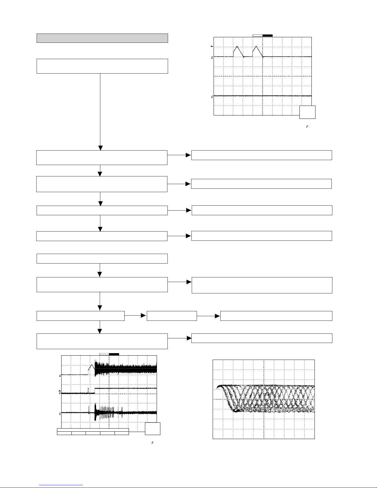
CD-DD4500
– 52 –
Vp-p=1.0 V~1.3 V
0.5 mV/div,0.5 µsec/div
T
FDO
DRF
TE
Stopped
CH1=500 mV
DC 10:1
CH2=10 V
DC 10:1
CH3=1 V
DC 10:1
500 ms/div
(500 ms/div)
NORM:20 kS/s
1
2
3
=Record Length=
Smoothing : ON CH1 : 0.000 V
CH2 : 0.0 V
Main : 100 K
Zoom : 2 K
Mode : AUTO
Type : EDGE CH1
Delay : 0.0 ns
Hold off : 0.2 µs
CH3 : 0.00 V
CH4 : 0.00 V
BW : FULL
=Trigger==Filter= =Offset=
-3 div -1 div 0 div +1 div +3 div
CH Position To
CH2
Position
0.20 div
T
FDO
TDO
Stopped
CH1=500 mV
DC 10:1
CH3=500 mV
DC 10:1
500 ms/div
(500 ms/div)
NORM:20 kS/s
1
3
=Record Length=
Smoothing : ON CH1 : 0.000 V
CH2 : 0.0 V
Main : 100 K
Zoom : 2 K
Mode : AUTO
Type : EDGE CH1
Delay : 0.0 ns
Hold off : 0.2 µs
CH3 : 0.000 V
CH4 : 0.00 V
BW : FULL
=Trigger==Filter= =Offset=
CH1
v/DIV
500 mV
If the level is not normal.
1. Is focus servo activated ?
(Waveform drawing Figure 52-2)
Pins 7~11, 79 and 80 on IC1
Check the laser diode driver Q1 peripheral circuit.
When a disc is loaded, start playback operation.
2. Does DRF change from "L" to "H" ?
Is the disc rotating ?
3. Is the HF waveform normal ? (Waveform drawing
Figure 52-3)
Check the spin system.
If the disc is spinning and a HF waveform is generated,
DRF will go H.
Figure 52-1
Check the laser diode driver Q1 peripheral circuit.
(1) Focus-HF system check.
Although a CD is inserted and the cover is closed, "NO
DISC" is displayed.
1. Does the pickup move to the PICKUP-IN Switch (SW4)
position ?
Sled motor (M2).
Press the OPEN/CLOSE switch (SW1) without inserting a
disc, and try starting the playback operation.
2. Does the focus (lens) move up and down ?
(Waveform drawing Figure 52-1)
Check the focus peripheral circuit.
3. Is the laser lit ?
Spindle motor (M1).
4. Is the turntable rotating ?
Figure 52-2
Figure 52-3
Yes
Yes
Yes
No
No
No
No
No
No
No
Yes
Yes
No
Page 53

– 53 –
CD-DD4500
T
T
FDO
SPDO
Stopped
CH1=200 mV
DC 10:1
CH2=500 mV
DC 10:1
500 ms/div
1999/04/07 09:51:15
(500 ms/div)
NORM:20 kS/s
2
1
=Record Length=
Smoothing : ON CH1 : 0.000 V
CH2 : 0.000 V
Main : 100 K
Zoom : 2 K
Mode : NORMAL
Type : EDGE CH2
Delay : 2.924 ms
Hold off : 0.2 µs
CH3 : 0.00 V
CH4 : 0.00 V
BW : FULL
=Trigger=
=Filter= =Offset=
T
T
TE
DRF
Stopped
CH1=10 V
DC 10:1
CH2=1 V
DC 10:1
100 ms/div
(100 ms/div)
NORM:100 kS/s
2
1
=Record Length=
Smoothing : ON CH1 : 0.0 V
CH2 : 0.00 V
Main : 100 K
Zoom : 2 K
Mode : NORMAL
Type : EDGE CH1
Delay : 2.924 ms
Hold off : 0.2 µs
CH3 : 0.00 V
CH4 : 0.00 V
BW : FULL
=Trigger=
=Filter= =Offset=
The tracking servo is not activated.
Check the peripheral circuits at pins 14, 15 and 20 on IC1, and
CNS1A/B.
If the waveform shown in Figure 53-1 appears and soon after
NO DISC appears ?
(2) Tracking system check.
Check the TE waveform at pin 15 on IC1.
A normal jump operation cannot be completed or the beginning of
the track cannot be found.
Check the around pin 20 on IC1.
"Initialization" is possible, but play is not possible ?
Data cannot be read. Check the VCO-PLL system.
"Initialization" is not possible.
Figure 53-1
Figure 53-2
Press the OPEN/CLOSE switch without inserting a disc, and
then try starting the play operation.
(3) Spin system check.
The spin driver circuit is OK.
1. The turntable rotates a little ? (Waveform drawing
Figure 53-2)
Check around pin 22 on IC1, pins 15 and 16 on IC3, and CNS3A/B.
2. The turntable doesn't rotate.
No
Yes
No
Yes
Yes
No
Page 54
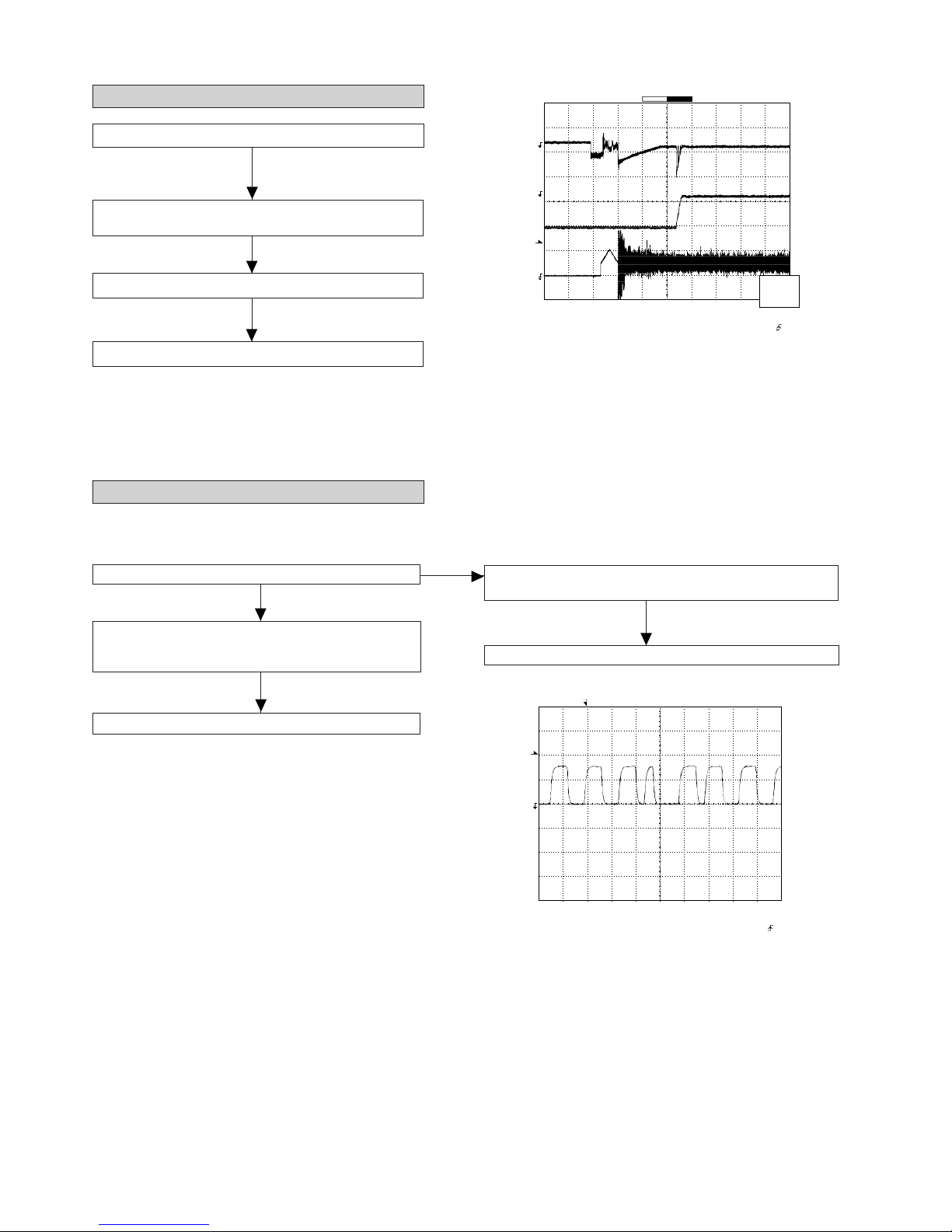
CD-DD4500
– 54 –
T
T
DOUT
Stopped
CH1=2 V
DC 10:1
500 ns/div
1999/04/07 09:25:28
(500 ns/div)
NORM:200 MS/s
1
=Record Length=
Smoothing : ON CH1 : 0.00 V
CH2 : 0.00 V
Main : 1 K
Zoom : 100
Mode : NORMAL
Type : EDGE CH1
Delay : 2.887 ms
Hold off : 0.2 µs
CH3 : 0.00 V
CH4 : 0.00 V
BW : FULL
=Trigger=
=Filter= =Offset=
T
FDO
PDO2
PDO1
Stopped
CH1=500 mV
DC 10:1
CH3=1 V
DC 10:1
CH4=1 V
DC 10:1
500 ms/div
(500 ms/div)
NORM:20 kS/s
1
4
3
=Record Length=
Smoothing : ON CH1 : 0.000 V
CH2 : 0.0 V
Main : 100 K
Zoom : 2 K
Mode : AUTO
Type : EDGE CH2
Delay : 0.0 ns
Hold off : 0.2 µs
CH3 : 0.00 V
CH4 : 0.00 V
BW : FULL
=Trigger==Filter= =Offset=
CH1
v/DIV
500 mV
1999/04/05 17:33:17
Is pin 52 (C2F) on IC1 "L" ?
Yes
No
The HF waveform is normal and the time is displayed
normally, but no sound is produced. Or the sound
has dropouts.
(5) Others.
There are too many error flags on a damaged disc which
makes error correction impossible.
Check again using a known good disc.
1. When playing at normal speed
Check the peripheral circuit at pin 39 (DOUT) on IC1 and
the waveform (Figure 54-2).
If OK, Check the unit.
When a disc is loaded, start play operation.
(4) PLL system check.
The HF waveform is normal, but the TOC data cannot be
read.
Check the PDO waveform. (Figure 54-1)
Check around pins 73~78 on IC1.
Figure 54-1
Figure 54-2
Page 55

– 55 –
CD-DD4500
FUNCTION T ABLE OF IC
IC1 VHiLC78645NE1: CD Servo (LC78645NE) (1/2)
1 SLC0 Output — Control output.
2 SLCIST Input —
Resistor connection terminal for SLCO output current
setting.
3 EFMIN Input — RF signal input terminal.
4 RF Output — RF signal monitor terminal.
5 RFVDD Input — RF power terminal.
6 RFVSS — — RF earth terminal. To be connected to 0 V.
7 FIN1 Input — A+C signal input terminal.
8 FIN2 Input — B+D signal input terminal.
9 TIN1 Input — E signal input terminal.
10 TIN2 Input — F signal input terminal.
11 VREF Output RFVDD/2 VREF voltage output terminal.
12 REFI Input — Reference supply setting terminal.
13* FE Output ZHI FE signal monitor terminal.
14 TEC Output – LPF capacitor connection terminal for TE signal.
15* TE Output ZHI TE signal monitor terminal.
16* RFMON Output ZHI RF internal signal monitor terminal.
17 JITTC – — Capacitor connection terminal for jitter detection.
18 ADAVDD Input — Power terminal for servo A/D, D/A.
19 ADAVSS — — Earth terminal for serve A/D, D/A. To be connected to 0 V.
20 TD0 Output ADAVDD/2 Output terminal for tracking control. D/A output.
21 FD0 Output ADAVDD/2 Output terminal for focus control. D/A output.
22 SPD0 Output ADAVDD/2 Output terminal for spindle control. D/A output.
23 SLD0 Output ADAVDD/2 Output terminal for sled control. D/A output.
24* GPDAC Output ADAVDD/2 Servo D/A general-purpose output terminal.
25 CONT4 Input/Output Input Mode General-purpose I/O terminal 4.
26 CONT5 Input/Output Input Mode General-purpose I/O terminal 5.
27* SBCK/CONT6 Input/Output Input Mode General-purpose I/O terminal 6 or
Subcode reading clock input terminal.
28 SBCK/FG Input — Subcode reading clock input terminal/FG signal input terminal/external
emphasis setting terminal. Terminal functions are set by commands. When
not used, connect to 0 V.
29* DEFECT Output L Defect terminal.
30* V/*P Output H Auto switching monitor output terminal for rough servo phase control. “H”:
rough servo, “L”: phase servo.
31* FSEQ Output L Sync signal detection output terminal.
The status changes to “H” when the sync signal detected in EFM and the
sync signal of internal generation are identified.
32* MONI1 Output L Internal signal monitor terminal 1.
33* MONI2 Output L Internal signal monitor terminal 2.
34* MONI3 Output L Internal signal monitor terminal 3.
35* MONI4 Output L Internal signal monitor terminal 4.
36* MONI5 Output L Internal signal monitor terminal 5.
37 VSS — — Digital system earth terminal. To be connected to 0 V.
38 VDD Input — Digital system power terminal.
39 DOUT Output L Digital OUT output terminal. (EIAJ format)
40 TEST Input L Input terminal for test. To be connected to 0 V.
41 LVDD Input — Power supply for Left channel.
42* LCH0 Output LVDD/2 Left channel output.
43 LVSS — — GND for Left channel. Must be connected to 0 V.
Pin No.
Function
Terminal Name
Input/Output
Setting in Reset
Controlled by commands from the
microcomputer. When not used, set
them as input terminals and connect
to 0 V, or set them as output
terminals and leave open.
In this unit, the terminal with asterisk mark (*) is (open) terminal which is not connected to the outside.
Left channel
D/A converter
For slice level
control.
Page 56

CD-DD4500
– 56 –
44 RVSS — — GND for Right channel. Must be connected to 0 V.
45* RCHO Output LVDD /2 Right channel output.
46 RVDD Input — Power supply for Right channel.
47 XVDD Input — Power supply for crystal oscillator.
48 XOUT Output — Connected for the 33.8688 MHz crystal oscillator ciement.
49 XIN Input —
50 FSX/16MIN Input/Output Input 7.35 kHz Synchronization signal monitor port.
or Clock input port for Digital filter & D/A
51 XVSS — — Crystal GND for crystal oscillator. Must be connected to 0 V.
Oscillator
52* C2F Output H C2 FLAG monitor port.
53* EFLG Output L C1, C2 error corrected monitor port.
54* 16MOUT Output Clock 16.9344 MHz output port.
55 ASLRCK Input — Word clock input port.
(If this port does not use, must be connect to 0 V.)
56 ASDACK Input — Bit clock input port.
(If this port does not use, must be connect to 0 V.)
57 ASDFIN Input —
Left/Right channel data input port.
(If this port does not use, must be connect to 0 V.)
58* LRSY Output L Word clock output port.
59* DATACK Output L Digital data Bit clock output port.
60* DATA Output L Left/Right channel data output port.
61 CE Input — Chip enable signal input port.
62 CL Input —
Microcomputer
Data transfer clock input port.
63 DI Input — Interface Data input port.
64 DO Output (H) Data output port. (N-ch. open drain output.)
65 *WRQ Output H Interruption signal output.
66 *RES Input — Chip reset signal input port.
This port must be set LOW after first applied power on.
67 DRF Output L Focus detection output port.
68 VDD5 Input — Power supply for Microprocessor.
69 VSS — — GND for digital circuit. Must be connected to 0 V.
70 CONT3 Input/Output Input General purpose port 1.
71 CONT2 Input/Output Input General purpose port 2.
72* CONT1 Input/Output Input General purpose port 3.
73 PDO1 Output — Internal VCO control phase comparator output port 1.
74 PDO2 Output Input Internal VCO control phase comparator output port 2.
75 VVSS — — GND for internal VCO.Must be connected to 0 V.
76 PCKIST Input — PDO output current adjustment resistor connection port.
77 VVDD Input — Power supply for internal VCO.
78 FR Input — VCO frequency range adjustment port.
79 LDS Input — LASER power detected signal input port.
80 LDD Output — LASER power control signal output port.
IC1 VHiLC78645NE1: CD Servo (LC78645NE) (2/2)
Pin No.
Function
Terminal Name
Input/Output
Setting in Reset
Right channel
D/A converter
Crystal
Oscillator
Anti-shock
Controlled with serial data command from microcomputer. When not used, General purpose input/
output terminal 7. set it as the input terminal and open
it by connecting to 0 V, or set it as the output terminal
and open it.
PLL
In this unit, the terminal with asterisk mark (*) is (open) terminal which is not connected to the outside.
Be sure to supply the same potential to each power terminal. (VVDD, ADAVDD, VDD, LVDD, RVDD, XVDD)
Terminal witch is controlled by the power terminal (VDD5 V) for a microcomputer interface :
CE (61 pin), CL (62 pin), DI (63 pin), DO (64 pin), WRQ (65 pin), RES (66 pin), DRF (67 pin)
Page 57

– 57 –
CD-DD4500
Figure 57 BLOCK DIAGRAM OF IC
IC1 VHiLC78645NE1: CD Servo (LC78645NE)
1
2
3
4
5
6
7
8
9
10
11
12
13
14
15
16
17
18
19
20
21 22 23 24 25 26 27 28 29 30 31 32 33 34 35 36 37 38 39 40
80 79 78 77 76 75 74 73 72 71 70 69 68 67 66 65 64 63 62 61
60
59
58
57
56
55
54
53
52
51
50
49
48
47
46
45
44
43
42
41
SLC0
SLCIST
EFMIN
RF
RFVDD
RFVSS
FIN1
FIN2
TIN1
TIN2
VREF
REFI
FE
TEC
TE
RFMON
JITTC
ADAVDD
ADAVSS
TD0
FD0
SPD0
SLD0
GPDAC
CONT4
CONT5
SBCK/CONT6
SBCK/FG
DEFECT
V/*P
FSEQ
MONI1
MONI2
MONI3
MONI4
MONI5
(3.3V)VSS
VDD
DOUT
TEST
LDD
LDSFRVVDD
PCKIST
VVSS
PD02
PD01
CONT1
CONT2
CONT3
VSS
VDD5
DRF
*RES
*WRQDODICLCE
DATA
DATACK
LRSY
ASDFIN
ASDACK
ASLRCK
16MOUT
EFLG
C2F
XVSS
FSX/16MIN
XIN
XOUT
XVDD
RVDD
RCH0
RVSS
LVSS
LCH0
LVDD
LC78645NE
+
–
+
–
+
–
+
–
–
–
+
+
MIX
LPF
LPF
LPF
TBAL
TBAL
RAM
LEVEL SET
AGC EQ
SW
PH
BH
+
–
+
–
+
–
+
–
MONI
CONT
A/D
SERVO PROCESSOR
TRACK JUMP
AUTO ADJUST
JITTER
DETECT
1bit DAC
8FS
DIGITAL FILTER
GENERAL-PURPOSE
PORTS
COMMAND
INTERFACE
CLOCK
GENERATOR
CLV,CAV
CONTROL
PLL
VCEC
SLICE LEVEL
CONTROL
APC
S/H
D/A
SW
DRF
RUPTURE DEFECT
FRAME SYNC
DETECT,PROTECT INSERT,
EFN DECODE
VDD
SUBCODE DECODE CRC
MONITOR SIGNAL SELECTOR
RAM
ERROR
CORRECTION
AUDIO CD
AUDIO OUT
SERIAL
OUT
EXTERNAL
AUDIO IN
INTERPOLATION
MUTE
ATTENUATION
DEEMPHSIS
LPF
FIN1
FIN2
TIN1
TIN2
REF1
DETECT
ADIN
ADAVDD
ADAVSS
JITTC
SLC0
EFMIN
SLCIST
PCK
PDO1
PDO2
FR
PCKIST
VVDD
VVSS
SBCK/FG
XIN
XOUT
16MOUT
XVDD
XVSS
*RES
*WRQ
CL
CE
DI
DO
VDD5V
CONT1, 2, 3
TEST
CONT4, 5
SBCK/CONT6
LVDD
LVSS
LCHO
RCHO
RVDD
RVSS
ASDFIN
ASDQCK
ASLRCK
DATA
DATACK
LRSY
DOUT
EFLG
C2F
FSK/16MIN
MONI1~5
VSS
VDD
V/*P
FSEQ
DRF
GPDAC
SPD0
SLD0
TD0
FD0
LDS
LDD
VREF
RFMON
RFVSS
RFVDD
RF
TEC
TE
FE
Page 58

CD-DD4500
– 58 –
1 RST Input Hardware reset input terminal. (L: reset, R: normal operation)
2* MIMD Input Microcomputer I/F mode select input terminal. (L: serial, H: I2C bus)
3 MICS Input Microcomputer I/F chip select input terminal.
4 MILP Input Microcomputer I/F latch pulse input.
5 MIDIO Input/Output Microcomputer I/F data input/output terminal.
6 MICK Input Microcomputer I/F clock input terminal.
7 MIACK Output Microcomputer I/F acknowledge output terminal.
8* FI0 Input Flag input terminal 0.
9* FI1 Input Flag input terminal 1.
10* FI2 Input Flag input terminal 2.
11* FI3 Input Flag input terminal 3.
12* IRQ Input Interrupt input terminal.
13 VSS — Digital ground terminal.
14 LRCKA Input Audio I/F LR clock input terminal A.
15 BCKA Input Audio I/F bit clock input terminal A.
16 SDO0 Output Audio I/F data output terminal 0.
17 SDO1 Output Audio I/F data output terminal 1.
18 SDO2 Output Audio I/F data output terminal 2.
19* SDO3 Output Audio I/F data output terminal 3.
20 LRCKB Input Audio I/F LR clock input terminal B.
21 BCKB Input Audio I/F bit clock input terminal B.
22 SDI0 Input Audio I/F data input terminal 0.
23 SDI1 Input Audio I/F data input terminal 1.
24 VDD Input Digital power supply terminal.
25 LRCKOA Output Audio I/F LR clock output terminal A.
26 BCKOA Output Audio I/F bit clock output terminal A.
27 TEST0 Input Test input terminal 0. (L: test, H: normal operation)
28 TEST1 Input Test input terminal 1. (L: test, H: normal operation)
29* LRCKOB Output Audio I/F LR clock output terminal B.
30* BCKOB Output Audio I/F bit clock output terminal B.
31* TXO Output SPDIF output terminal.
32 TEST2 Input Test input terminal 2. (L: test, H: normal operation)
33 TEST3 Input Test input terminal 3. (L: test, H: normal operation)
34 RX Input SPDIF input terminal.
35 VSS — Digital ground terminal.
36 TSTSUB0 Input Test sub input terminal 0. (L: test, H: normal operation)
37 FCONT Output VCO frequency control output terminal.
38 TSTSUB1 Input Test sub input terminal 1. (L: test, H: normal operation)
39 TSTSUB2 Input Test sub input terminal 2. (L: test, H: normal operation)
40 PDO Output Phase error signal output terminal.
41 VDDA Input Analog power supply terminal.
42* PLON Input Clock select input terminal. (L: external clock, H: VCO clock)
43 AMPI Input Amplifier input terminal for LPF.
44 AMPO Output Amplifier output terminal for LPF.
45 CKI Input External clock input terminal.
46 VSSA — Analog ground terminal.
47 CKO Output DIR clock output terminal.
48 LOCK Output VCO lock detection output terminal.
49 VSS — Digital ground terminal.
50 WR Output External SRAM write signal output terminal.
51 OE Output External SRAM output enable signal output terminal.
IC504 RH-iX0443AWZZ: Dolby Decoder (IX0443AW) (1/2)
Terminal Name
Pin No.
Input/Output
Function
In this unit, the terminal with asterisk mark (*) is (open) terminal which is not connected to the outside.
Page 59

– 59 –
CD-DD4500
52 CE Output External SRAM chip enable signal output terminal.
53 VDD Input Digital power supply terminal.
54 IO7 Input/Output External SRAM data I/O terminal 7.
55 IO6 Input/Output External SRAM data I/O terminal 6.
56 IO5 Input/Output External SRAM data I/O terminal 5.
57 IO4 Input/Output External SRAM data I/O terminal 4.
58 IO3 Input/Output External SRAM data I/O terminal 3.
59 IO2 Input/Output External SRAM data I/O terminal 2.
60 IO1 Input/Output External SRAM data I/O terminal 1.
61 IO0 Input/Output External SRAM data I/O terminal 0.
62 VSS — Digital ground terminal.
63 AD0 Output External SRAM address output terminal 0.
64 AD1 Output External SRAM address output terminal 1.
65 AD2 Output External SRAM address output terminal 2.
66 AD3 Output External SRAM address output terminal 3.
67 AD4 Output External SRAM address output terminal 4.
68 AD5 Output External SRAM address output terminal 5.
69 AD6 Output External SRAM address output terminal 6.
70 AD7 Output External SRAM address output terminal 7.
71 VDD Input Digital power supply terminal.
72 AD8 Output External SRAM address output terminal 8.
73 AD9 Output External SRAM address output terminal 9.
74 AD10 Output External SRAM address output terminal 10.
75 AD11 Output External SRAM address output terminal 11.
76 AD12 Output External SRAM address output terminal 12.
77 AD13 Output External SRAM address output terminal 13.
78 AD14 Output External SRAM address output terminal 14.
79 AD15 Output External SRAM address output terminal 15.
80 AD16 Output External SRAM address output terminal 16.
81 VSS — Digital ground terminal.
82 PO0 Output General-purpose output terminal 0.
83 PO1 Output General-purpose output terminal 1.
84 PO2 Output General-purpose output terminal 2.
85 PO3 Output General-purpose output terminal 3.
86* PO4 Output General-purpose output terminal 4.
87* PO5 Output General-purpose output terminal 5.
88* PO6 Output General-purpose output terminal 6.
89* PO7 Output General-purpose output terminal 7.
90 VDDDL Input Power supply terminal for DLL.
91 LPFO Output LPF output terminal for DLL.
92* DLON Input DLCKS terminal DLON terminal DLL clock setting
"L" "L" SCKI input. (DLL circuit off)
93* DLCKS Input
"L" "H" Quadruple of XI clock
"H" "L" Triple of XI clock
"H" "H" Sextuple ofXI clock
94 SCKO Output ASP clock output terminal.
95 VSSDL — Ground terminal for DLL.
96 SCKI Input External system clock input terminal.
97 VSSX — Ground terminal for crystal oscillation circuit.
98 XO Output Crystal oscillation output terminal.
99 XI Input Crystal oscillation input terminal.
100 VDDX Input Power supply terminal for crystal oscillation circuit.
IC504 RH-iX0443AWZZ: Dolby Decoder (IX0443AW) (2/2)
Terminal Name
Pin No.
Input/Output
Function
In this unit, the terminal with asterisk mark (*) is (open) terminal which is not connected to the outside.
Page 60

CD-DD4500
– 60 –
Figure 60 BLOCK DIAGRAM OF IC
IRQ
SDin
SDOn
LRCK/BCK
RX
LOCK
/RST
MIMD
/MICS
/MILP
MIDIO
/MICK
MIACK
TXO
FIn
POn
IOn
ADn
/CE,/OE,/WR
LPFO
DLON
SCKI
SCKO
ROM
4 kword x 3
RAM
128 word
40 bit
XRAM
4 kword
YRAM
4 kword
CROM
4 kword
ERAM
4 kword
DLL
3
17
8
8
4
DIT
AYAXMZMYMX
ALUMAC
X0,X1,X2
Y0,Y2,Y3
A1 A0 A2 A3
DIR
4
2
I bus
Y bus
X bus
PROGRAM
EXECUTE
CONTROL
PROGRAM
INSTRUCTION
DECODER
INTERRUPT
CONTROL
AUDIO
I/F
TIMER
MICROCOMPUTER
I/F
REGISTER
ROUND OFF/LIMIT ROUND OFF/LIMIT
ADRESS OPERATION
X2
C POINTER
REGISTER
Y POINTER
REGISTER
X POINTER
REGISTER
BUS
SWITCH
TIMING
EXTERNAL
SRAM I/F
GENERAL-PURPOSE
OUTPUT PORT
FLAG
IC504 RH-iX0443AWZZ: Dolby Decoder (IX0443AW)
Page 61

– 61 –
CD-DD4500
1 SDOS Input SDTO source select pin. (Note 1)
“L”: internal ADC output, “H”: I2C DAUX input
2 I2C Input Serial control mode select pin. “L”: 3-wire serial, “H”: I2C bus
3 SMUTE Input Software mute pin. (Note 1)
Software mute is started with “H” and canceled with “L”.
4 BICK Input Audio serial data clock pin.
5 LRCK Input Input channel clock pin.
6 SDTI1 Input DAC1 audio serial data input pin.
7 SDTI2 Input DAC2 audio serial data input pin.
8 SDTI3 Input DAC3 audio serial data input pin.
9 SDTO Output Audio serial data output pin.
10 DAUX Input Auxiliary audio serial data input pin.
11 DFS Input Double-speed sampling mode pin. (Note 1)
“L”: normal speed, “H”: double speed
12* N.C. — Not connect.
13 DZFE Input Zero input detection function enable pin.
“L”: mode 7 (disable) in parallel mode, selectable with DZFM2-0 bit in serial mode.
“H”: mode 0 (output from DZF1 with AND of 6 ch)
14 TVDD Input Power supply pin for output buffer, 2.7 V - 5.5 V.
15 DVDD Input Digital power supply pin, 4.5 V - 5.5 V.
16 DVSS — Digital ground pin, 0 V.
17 PDN Input Power down & reset pin. When this pin is switched to “L”, it enters the power down state
and the register is initialized. Reset it with the PDN pin if P/S and CAD0-1 are changed.
18 TST Input Test pin. Connect it to DVSS.
19* N.C. — Not connect.
20 ADIF Input Analog input type select pin. “H”: differential input, “L”: single end input
21 CAD1 Input Chip address 1 pin.
22 CAD0 Input Chip address 0 pin.
23 LOUT3 Output DAC3 L channel analog output pin.
24 ROUT3 Output DAC3 R channel analog output pin.
25 LOUT2 Output DAC2 L channel analog output pin.
26 ROUT2 Output DAC2 R channel analog output pin.
27 LOUT1 Output DAC1 L channel analog output pin.
28 ROUT1 Output DAC1 R channel analog output pin.
29 LIN- Input L channel analog inversion input pin.
30 LIN+ Input L channel analog non-inversion pin.
31 RIN- Input R channel analog inversion input pin.
32 RIN+ Input R channel analog non-inversion pin.
33* DZF2 Output Zero input detection 2 pin. (Note 2)
If the group 2 input data has been “0” for 8,192 consecutive times or the RSTN bit is “0”, it
changes to “H”.
OVF Output Analog input overflow detection pin. (Note 3)
It changes to “H” when the analog input to L-ch or R-ch overflows.
34 VCOM Output Common voltage output pin, AVDD/2
Mount a capacitor of large capacity (approx. 2.2 µF) to remove power source noise.
35 VREFH Input Reference voltage input pin, AVDD.
36 AVDD Input Analog power supply pin, 4.5 V - 5.5 V.
37 AVSS — Analog ground pin, 0 V.
38* DZF1 Output Zero input detection 1 pin. (Note 2)
If the group 1 input data has been “0” for 8,192 consecutive times or the RSTN bit is “0”, it
changes to “H”.
39* MCLK Input Master clock input pin.
40 P/S Input Parallel/serial select pin.
“L”: serial control mode, “H”: parallel control mode
IC505 RH-iX0454AWZZ: 6-CH CODEC IC (AK4527BVQ) (1/2)
Terminal Name
Pin No.
Input/Output
Function
In this unit, the terminal with asterisk mark (*) is (open) terminal which is not connected to the outside.
Page 62

CD-DD4500
– 62 –
Figure 62 BLOCK DIAGRAM OF IC
IC505 RH-iX0454AWZZ: 6-CH CODEC IC (AK4527BVQ) (2/2)
Terminal Name
Pin No.
Input/Output
Function
41 DIF0 Input Audio data interface format 0 pin. (in parallel control mode)
CSN Input Chip select pin. (in 3-wire serial control mode)
Connect it to DVDD in I2C bus control mode.
42 DIF1 Input Audio data interface format 1 pin. (in parallel control mode)
SCL/CCLK Input Control data clock pin. (in serial control mode)
I2C = “L”: CCLK (3-wire serial), I2C = “H”: SCL (I2C bus)
43 LOOP0 Input Loopback mode 0 pin. (in parallel control mode)
Enables digital loopback from ADC to all DACs.
SDA/CDTI Input/Output Control data input pin (in serial control mode)
I2C = “L”: CDTI (3-wire serial), I2C = “H”: SDA (I2C bus)
44 LOOP1 Input Loopback mode 1 pin. (Note 1)
Input from SDTI1 to all DACs.
Notes:
1. When P/S = “L”, the register and OR are assigned to SDOS, SMUTE, DFS and LOOP1 pins.
2. When P/S = “L” and DZFE = “L”, the groups 1 and 2 are selectable with DZM2-0 bit.
3. This pin changes to OVF pin when OVFE bit is set to “1” in the serial control mode.
4. Do not float any input pins.
ADC
ADC
HPF
Audio
I/F
HPF
DATTDACLPF
DATTDACLPF
DATTDACLPF
DATTDACLPF
DATTDACLPF
DATTDACLPF
LIN+
LIN-
RIN+
RIN-
LOUT1
ROUT1
LOUT2
ROUT2
LOUT3
ROUT3
AK4527B
MCLK
MCLK
LRCK
LRCK
BICK
BICK
DAUX
SDOS
SDTO
SDTI1
SDTI2
SDTI3
SDIN1
SDIN2
SDIN3
SDOUT
Format
Converter
LRCK
BICK
SDIN
SDOUT1
SDOUT2
SDOUT3
AC3
RX1 RX2 RX3 RX4
XTI
XTO
MCKO
LRCK
BICK
SDTO
DIR
AK4112A
Page 63

– 63 –
CD-DD4500
IC601 VHiLC75341/-1: Audio Processor (LC75341)
Figure 63 BLOCK DIAGRAM OF IC
19
20
21
222324
123
4
5
6
7
8
9
10 11 12 13 14 15 16
18
17
LVref
RVref
CONTROL
CIRCUIT
CONTROL
CIRCUIT
CONTROL
CIRCUIT
LOUT
LBASS
0.1uF
LIN
LSEL0
L4
L3
L2 L1
R1 R2
R3 R4
RSEL0
R1N
RTRELTRE
RBASS
0.1uF
ROUT
Yref
VDD
CL
DI
CE
YSS
CCB
INTERFACE
CD
Tuner
Tape
Video
24 23 22 21 20 19 18 17 16 15 14 13
123456789101112
LC75341
DI
CE
VSS
LOUT
LBASS
LTRE
LIN
LSEL0
L4
L3
L2
L1
CL
VDD
VREF
ROUT
RBASS
RTRB
RIN
RSEL0R4R3
R2
R1
Page 64

CD-DD4500
– 64 –
1*-4* OUT4-OUT1 Port output.
5 AVDD Analog positive power supply terminal.
6 SWin Volume input.
7 GNDS GND terminal.
8 SRin Volume input.
9 SLin Volume input.
10 GNDC GND terminal.
11 Cin Volume input.
12 GNDR GND terminal.
13 Rin Tone input.
14 GNDL GND terminal.
15 Lin Tone input.
16 BYPASSR Volume input to L/R when bypassed.
17 BYPASSL Volume input to L/R when bypassed.
18 LTRE
Tone treble frequency adjustment terminal.
19 LBASS3
Tone bass frequency adjustment terminal.
20 LBASS2
Tone bass frequency adjustment terminal.
21 LBASS1
Tone bass frequency adjustment terminal.
22 CR2 Tone output terminal.
23 RBASS2
Tone bass frequency adjustment terminal.
IC602 VHiM62446FP-1: 6-Ch Electronic Volume (M62446FP)
Terminal
Name
Pin
No.
Function
24 RBASS3
Tone bass frequency adjustment terminal.
25 RTRE
Tone treble frequency adjustment terminal.
26 RBASS1
Tone bass frequency adjustment terminal.
27 CR1 L/R volume input.
28 CL2 Tone output terminal.
29 CL1 L/R volume input.
30 AVSS Analog negative power supply terminal.
31 Lout L output.
32 Rout R output.
33 Cout Volume output.
34 SLout Volume output.
35 SRout Volume output.
36 SWout Volume output.
37 AGND Analog GND terminal.
38 DGND Digital GND terminal.
39 LATCH Latch input terminal.
40 DATA Data input terminal.
41 CLK Clock input terminal for data transfer.
42 DVDD Digital power supply terminal.
Terminal
Name
Pin
No.
Function
Figure 64 BLOCK DIAGRAM OF IC
1
2
3
4
5
6
7
8
9
10
11
12
13
14
15
16
17
18
19
20
21
33
34
35
36
37
38
39
40
41
42
32
31
30
29
28
27
26
25
24
23
22
OUT4
OUT3
OUT2
OUT1
AVDD
SWin
GNDS
SRin
SLin
GNDC
Cin
GNDR
Rin
GNDL
Lin
BYPASSR
BYPASSL
LTRE
LBASS3
LBASS2
LBASS1
DVDD
CLK
DATA
LATCH
DGND
AGND
SW out
SRout
SLout
Cout
Rout
Lout
AVSS
CL1
CL2
CR1
CR2
RTRE
RBASS3
RBASS2
RBASS1
OUTPUT
PORT
MCU
I/F
volume
volume
volume
volume
volume
volume
tonetone
In this unit, the terminal with asterisk mark (*) is (open) terminal which is not connected to the outside.
Page 65

– 65 –
CD-DD4500
1 AVDD AVDD Input Analog VDD.
2 ANI0 TUN-SM Input RDS VSM
3 ANI1 SPEANA 3 Input SPEANA data input. L, R 16 kHz
4 ANI2 SPEANA 2 Input SPEANA data input. L, R 63 Hz
5 ANI3 SPEANA 1 Input SPEANA data input. L, R 1 kHz
6 ANI4
O/C SW Input CD open/close switch.
DISC NO SW Input CD disc number switch.
7-9 ANI5-ANI7
KEY 2-KEY 0 Input Key input.
PLAY SW_B Input Play switch for T 2.
10 ANI8
FPA Input TAPE 2 A-SIDE full proof.
FPB Input TAPE 2 B-SIDE full proof.
11 ANI9
HEADPHONE Input Headphone switch.
MIC-IN Input MIC-IN sw.
12 P02 DRF Input CD RF level detection.
13 P03 WRQ Input CD DSP write request.
14 AVSS AVSS — Analog ground.
15 VSS1 VSS1 — Ground voltage.
16 X1 X1 Input Main clock.
17 X2 X2 Output Main clock.
18 VDD1 VDD1 Input (+) Power supply
19 Vpp/IC Vpp/IC — GND
20 P20/TI00 CD CE Output CD CE output.
21 P25/SI0/RxD0 CD DO Input CD DSP CODE Q out/MPEG microcomputer data input.
22 P25/SO0/TxD0 CD DI Output CD DSP command/MPEG microcomputer command.
23 P25/SCK0/ASCHK0 CD CLK Output CD DSP clock/MPEG microcomputer clock.
24 P67/INTP2 P_IN Input Power failure control.
25 P66/TIO51 JOG 0 Input Key jog input 0.
26 P65/INTP1 JOG 1 Input Key jog input 1.
27 P64/INTP0 REMOCON Input Remocon input.
28 P63/TIO50 CE Output CE output.
29 P62/SCK1 CLK Output Clock output.
30 P61/SO1 DI Output Data output.
31 P60/SI1 DO Input Data input.
32 P57/SCK2 DD CLK Output Dolby decorder clock.
33 P56/SO2 DD DO Output Dolby decorder data out.
34 P55/SI2 DD DI Input Dolby decorder data in.
35 P54 DD ACK Input Dolby decorder ACK.
36 P53 DD LP Output Dolby decorder latch
37 P52 DD CS Output Dolby decorder CS.
38 P51 DD LOCK Input Dolby decorder lock.
39 P50 DD STATUS Input Dolby decorder status.
40 VSS0 VSS0 — Ground voltage.
41 VDD0 VDD0 Input (+) Power supply.
42 RESET RESET Input Microcomputer reset.
43 P47 T2 RUN Input TAPE 2 RUN PULSE input.
44 P46 CD CLAMP SW Input CD CHANGER CLAMP switch.
45 P45 DIGI_SEL Output CD FUNC: L/EXP FUNC: H
46 P44 RES OUT Output CD DSP reset & MPEG microcomputer reset.
47 P43 SP DET Input Speaker output detection.
48,49 P42,P41 LCK 2,LCK 1 Output LED driver LCK. (BU2092-1)
50 P40 T1 RUN Input TAPE 1 RUN PULSE input.
IC701 RH-iX0422AWZZ: System Microcomputer (IX0422AW) (1/2)
Port Name
Terminal Name
Pin No.
Input/Output
Function
Page 66

CD-DD4500
– 66 –
IC701 RH-iX0422AWZZ: System Microcomputer (IX0422AW) (2/2)
In this unit, the terminal with asterisk mark (*) is (open) terminal which is not connected to the outside.
Port Name Terminal NamePin No. Input/Output
Function
51* P107/FIP47 DIST_OUT (2) Output Distination output/switch output.
52 P106/FIP46 KARAOKE LATCH Output KARAOKE IC data latch. (When not used. Connect to 0 V)
53 P105/FIP45 6-ch VOL LATCH Output 6 ch VOL IC data latch.
54 P104/FIP44 NO USE Input Open
55 P103/FIP43 SPRLY (FRONT) Output (Front) Speaker output relay control.
56 P102/FIP42 SMUTE Output System mute control.
57 P101/FIP41 TIMER LED Output Timer LED control.
58 P100/FIP40 AC RLY_CONT Output AC relay control.
59 P97/FIP39 DIST_OUT Output Distination output/switch output.
60
P96/FIP38 SPN Input Tuner span change.
P96/FIP38 P25 Output FL display segment driver.
61-63 P95/FIP37-P93/FIP35 P24-P22 Output FL display segment driver.
64
P92/FIP34 DIST3 Input Distination input.
P92/FIP34 P21 Output FL display segment driver.
65
P91/FIP33 DIST2 Input Distination input.
P91/FIP33 P20 Output FL display segment driver.
66
P90/FIP32 DIST1 Input Distination input.
P90/FIP32 P19 Output FL display segment driver.
67
P87/FIP31 DIST0 Input Distination input.
P87/FIP31 P18 Output FL display segment driver.
68-74 P86/FIP31-P80/FIP24 P17-P11 Output FL display segment driver.
75-78 P77/FIP23-P74/FIP20 P10-P7 Output FL display segment driver.
79 VDD2 VDD2 Input (+) Power supply.
80 VLOAD VLOAD Input FL driver (-) power supp. -30 V
81-84 P73/FIP19-P70/FIP16 P6-P3 Output FL display segment driver.
85,86 FIP15,FIP14 P2,P1 Output FL display segment driver.
87-100 FIP13-FIP0 G14-G1 Output FL display segment driver.
Page 67

– 67 –
CD-DD4500
Input/OutputPort Name Terminal Name
1 VSS –– GND
2 DATA Input Serial data input.
3 CLOCK Input Shipt clock of data.
4 LCK Input Latch clock of data.
5 Q0 T_SOL B Output TAPE 2 SOLENOID control.
6 Q1 T_SOL A Output TAPE 1 SOLENOID control.
7 Q2 T_MOTOR Output Tape motor control.
8 Q3 PLAY_FWD LED Output Play forward LED.
9 Q4 STOP LED Output Stop LED.
10* Q5 L+ Output
11* Q6 L- Output
12* Q7 N.C. ––
13* Q8 CD DISC1 LED Output CD DISC 1 LED.
14* Q9 CD DISC2 LED Output CD DISC 2 LED.
15* Q10 CD DISC3 LED Output CD DISC 3 LED.
16* Q11 PLAY_REV LED Output Play reverse LED.
17 OE Input Output enable.
18 VDD Input Power.
Pin No.
IC702 VHiBU2092F/-1: Input/Output Expander (BU2092F)
1 VSS –– GND
2 DATA Input Serial data input.
3 CLOCK Input Shipt clock of data.
4 LCK Input Latch clock of data.
5 Q0 C-SPRLY Output Center speaker relay control.
6 Q1 S-SPRLY Output Surround speaker relay control.
7 Q2 SW-SPRLY Output Subwoofer speaker relay control.
8 Q3 2ch/6ch-RLY Output Speaker control.
9 Q4 SW-MUTE Output Subwoofer mute control.
10 Q5 T_BIAS Output Tape record bias.
11 Q6 T_T1/T2 Output Tape T 1/T 2 change.
12 Q7 REC/PLAY Output Tape Rec/Play change.
13 Q8 FAN CONT Output Fan control.
14 Q9 -11dBATT Output -11 dB attenuator.
15 Q10 N.C. ––
16 Q11 DD RESET Output Dolby decorder reset.
17 OE Input Output enable.
18 VDD Input Power.
IC181 VHiBU2092F/-1: Input/Output Expander (BU2092F)
Function
Input/OutputPort Name Terminal Name
Pin No.
Function
In this unit, the terminal with asterisk mark (*) is (open) terminal which is not connected to the outside.
Page 68

CD-DD4500
– 68 –
FL701 VVKBJ844GNK-1: FL Display
FL DISPLAY
11G 13G 14G 12G
9G8G7G6G5G4G3G2G1G10G
C O
C O
S1
S1
S1
S1
S1
S1
S1
S2
S3
S4
f
a
b
k
j
h
m
g
c
n
e
r
p
Dp
d
[ 1G ~ 8G ]
B24
B21
B20
B18
B9
B17
B17
B10
B12
B4
B2
B2
B4
B1
B5
B8
B16
B13
B9
B1
[ 11G ]
[ 13G ]
[ 12G ]
[ 14G ]
B18
B20
B10
B12
B5
B8
B16B13
B21
B24
S13
S9
S8
S7
S14
S15
S3
S2
S4
S5
S6
S10
S11
S12
S12
S13
S3
S2
S4
S1
S10
S6
S5
S7
S8
S9
S11
S1
Page 69
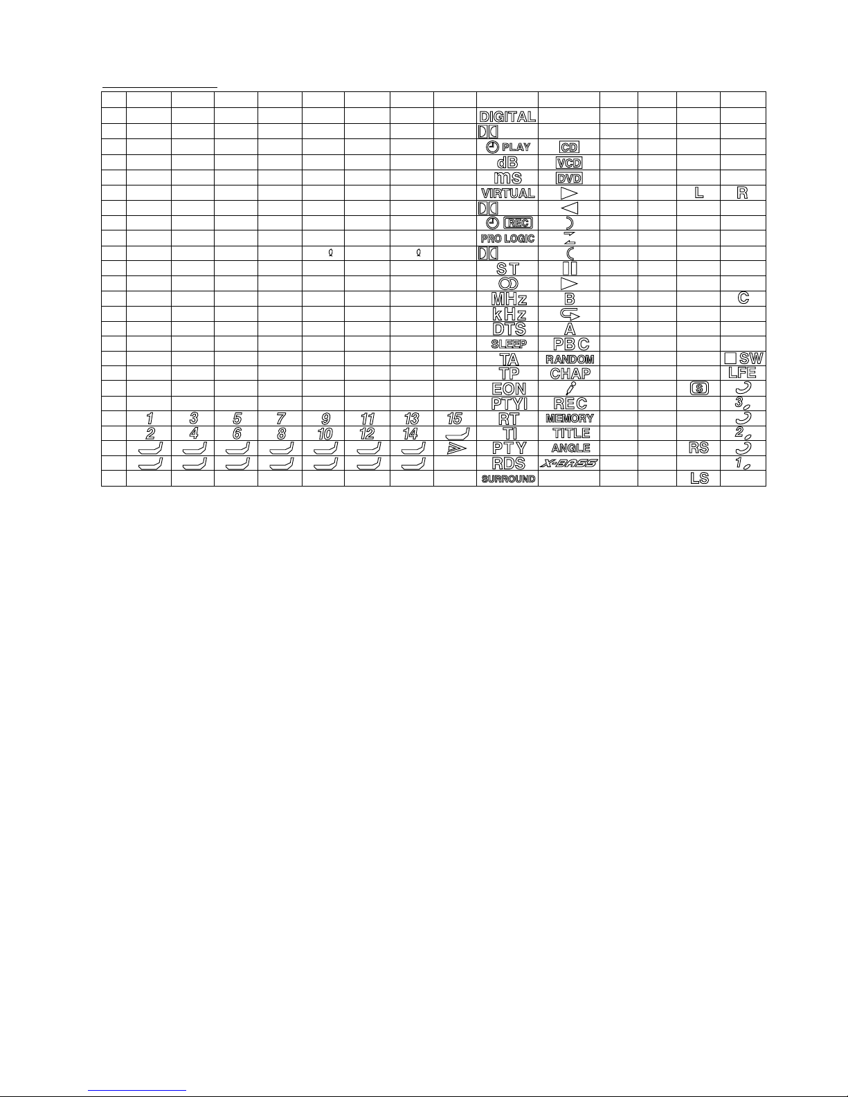
– 69 –
CD-DD4500
ANODE CONNECTION
1G 2G 3G 4G 5G 6G 7G 8G 9G 10G 11G 12G 13G 14G
P1
P2
P3
P4
P5
P6
P7
P8
P9
P10
P11
P12
P13
P14
P15
P16
P17
P18
P19
P20
P21
P22
P23
P24
P25
Dp
d
n
p
r
e
c
g
m
–
f
b
k
j
h
a
S4
S3
S2
S1
–
Dp
d
n
p
r
e
c
g
m
–
f
b
k
j
h
a
S4
S3
S2
S1
–
Dp
d
n
p
r
e
c
g
m
–
f
b
k
j
h
a
S4
S3
S2
S1
–
Dp
d
n
p
r
e
c
g
m
–
f
b
k
j
h
a
S4
S3
S2
S1
–
Dp
d
n
p
r
e
c
g
m
–
f
b
k
j
h
a
S4
S3
S2
S1
–
Dp
d
n
p
r
e
c
g
m
co
f
b
k
j
h
a
S4
S3
S2
S1
–
Dp
d
n
p
r
e
c
g
m
–
f
b
k
j
h
a
S4
S3
S2
S1
–
–
–
–
B17
B18
B19
B20
B21
B22
B23
B24
B9
B10
B11
B12
B13
B14
B15
B16
B1
B2
B3
B4
B5
B6
B7
B8
S1
B17
B18
B19
B20
B21
B22
B23
B24
B9
B10
B11
B12
B13
B14
B15
B16
B1
B2
B3
B4
B5
B6
B7
B8
S1
S1
S2
S3
S4
S5
S12
S13
–
–
–
–
–
–
–
–
S9
S8
S7
S6
S11
S10
S1
S2
S3
S4
S5
S14
S15
S7
S8
S9
S13
S10
S11
S12
S6
–
Dp
d
n
p
r
e
c
g
m
co
f
b
k
j
h
a
S4
S3
S2
S1
–
( 1 )
( 2 )
( 3 )
( 4 )
( 15 )
( 15 )
( 7 )
( 8 )
( 9 )
( 10 )
( 11 )
( 12 )
( 13 )
( 15 )
( 14 )
( DIGITAL )
( VIRTUAL )
(PRO LOGIC)
( 3 )
( 2 )
( 1 )
Page 70

CD-DD4500
– 70 –
–– MEMO ––
Page 71

– 71 –
CD-DD4500
PARTS GUIDE
NOTE:
Parts marked with “ ” are important for maintaining the safety of the set.
Be sure to replace parts with specified ones for maintaining the safety and performance of the set.
“HOW TO ORDER REPLACEMENT PARTS”
To have your order filled promptly and correctly, please furnish the
following information.
1. MODEL NUMBER 2. REF. No.
3. PART NO. 4. DESCRIPTION
MARK: SPARE PARTS-DELIVERY SECTION
For U.S.A. only
Contact your nearest SHARP Parts Distributor to order.
For location of SHARP Parts Distributor,
Please call Toll-Free;
1-800-BE-SHARP
Explanation of capacitors/resistors parts codes
Capacitors
VCC ....................... Ceramic type
VCK........................ Ceramic type
VCT........................ Semiconductor type
VC • • MF ............... Cylindrical type (without lead wire)
VC • • MN............... Cylindrical type (without lead wire)
VC • • TV................ Square type (without lead wire)
VC • • TQ ............... Square type (without lead wire)
VC • • CY ............... Square type (without lead wire)
VC • • CZ ............... Square type (without lead wire)
VC • • • • • • • • • J .. The 13th character represents capacity difference.
("J" ±5%, "K" ±10%, "M" ±20%, "N" ±30%,
"C" ±0.25 pF, "D" ±0.5 pF, "Z" +80-20%.)
If there are no indications for the electrolytic capacitors, error is ±20%.
Resistors
VRD ....................... Carbon-film type
VRS........................ Carbon-film type
VRN ....................... Metal-film type
VR • • MF ............... Cylindrical type (without lead wire)
VR • • MN............... Cylindrical type (without lead wire)
VR • • TV................ Square type (without lead wire)
VR • • TQ ............... Square type (without lead wire)
VR • • CY ............... Square type (without lead wire)
VR • • CZ ............... Square type (without lead wire)
VR • • • • • • • • • J .. The 13th character represents error.
("J" ±5%, "F" ±1%, "D" ±0.5%.)
If there are no indications for other parts, the resistors are ±5%
carbon-film type.
CD-DD4500 Mini Component System consisting of
CD-DD4500 (main unit), CP-DD4500 (Front), center
(GBOXS0064AWM1), surround (R) (GBOXS2008AWM1) and
surround (L) (GBOXS4008AWM1) speaker system.
MINI COMPONENT SYSTEM
MODEL CD-DD4500
Page 72

PRICE
RANK
DESCRIPTION
NO.
PARTS CODE
NO. PARTS CODE
PRICE
RANK
DESCRIPTION
CD-DD4500
CD-DD4500
INTEGRATED CIRCUITS
IC1 VHILC78645NE1 J AY CD Servo,LC78645NE
IC2 VHIM63001FP-1 J AX Focus/Tracking/Spin/Sled Driver,
M63001FP
IC101 VHIAN7345K/-1 J AM Playback and Record/Playback
Amp.,AN7345K
IC102 VHIBA3126N/-1 J AF Head Selector,BA3126N
IC181 VHIBU2092F/-1 J AM Input/Output Expander,BU2092F
IC302 VHILC72131/-1 J AP PLL (Tuner),LC72131
IC303 VHILA1832S/-1 J AN FM IF Det./FM Mpx./AM IF,
LA1832S
IC401 VHISTK40224-1 J BC Power Amp.,STK40224
IC501 VHPTORX178B-1 J Optical Fiber Data Link,
TORX178B
IC502 VHI74VHC00F-1 J AE Invertor,74VHC00F
IC504 RH-IX0443AWZZ J BM Dolby Decoder,IX443AW
IC505 RH-IX0454AWZZ J BB 6-ch Codec IC,AK4527BVQ
IC571 VHITA48M033-1 J AK 3.3V Voltage Regulator,
TA48M033F (S)
IC601 VHILC75341/-1 J AM Audio Processor,LC75341
IC602 VHIM62446FP-1 J AY 6-ch Electronic Volume,
M62446FP
IC605~607 VHINJM4565M-1 J AC Buffer Amp.,NJM4565M
IC701 RH-IX0442AWZZ J BA System Microcomputer,
IX0442AW
IC702 VHIBU2092F/-1 J AM Input/Output Expander,BU2092F
IC703,704 VHIKIA4558P-1 J AC Ope Amp.,KIA4558P
IC850 VHIKIA7810AP1 J AF Voltage Regulator,KIA7810AP
IC851 VHIKIA7805AP1 J AF Constant Voltage Regulator,
KIA7805AP
IC880 VHIKIA7805AP1 J AF Constant Voltage Regulator,
KIA7805AP
IC901,902 VHISTK40270N1 J AY Power Amp.,STK40270N
IC904 VHIKIA4558P-1 J AC Ope Amp.,KIA4558P
IC905,906 VHITC4053BP-1 J AE Triple 2-Channel Multiplexer,
TC4503BP
IC907 VHIKIA4558P-1 J AC Ope Amp.,KIA4558P
TRANSISTORS
Q1 VSKTA1266GR-1 J AB Silicon,PNP,KTA1266 GR
Q2 VSKTC3203Y/-1 J AC Silicon,NPN,KTC3203 Y
Q3 VSKRC102M//-1 J AC Digital,NPN,KRC102 M
Q101 VSKRC104M//-1 J AC Digital,NPN,KRC104 M
Q102,103 VSKTC3199GR-1 J AB Silicon,NPN,KTC3199 GR
Q121,122 VSKTC3199GR-1 J AB Silicon,NPN,KTC3199 GR
Q124 VS2SA1015GR-1 J AB Silicon,PNP,2SA1015 GR
Q126 VSKRC104M//-1 J AC Digital,NPN,KRC104 M
Q128 VSKTC3203Y/-1 J AC Silicon,NPN,KTC3203 Y
Q360 VSKTA1266GR-1 J AB Silicon,PNP,KTA1266 GR
Q371 VSKTA1266GR-1 J AB Silicon,PNP,KTA1266 GR
Q401~404 VS2SC2878B/-1 J AC Silicon,NPN,2SC2878 B
Q405,406 VSKTC3199GR-1 J AB Silicon,NPN,KTC3199 GR
Q407,408 VS2SC2878B/-1 J AC Silicon,NPN,2SC2878 B
Q409~413 VSKTC3199GR-1 J AB Silicon,NPN,KTC3199 GR
Q420 VSKRC107M//-1 J AC Digital,NPN,KRC107 M
Q421 VSKTA1271Y/-1 J AC Silicon,PNP,KTA1271 Y
Q422 VSKTC3203Y/-1 J AC Silicon,NPN,KTC3203 Y
Q423 VSKTC3199GR-1 J AB Silicon,NPN,KTC3199 GR
Q424 VS2SB1565F/-1 J AG Silicon,PNP,2SB1565 F
Q503 VSKRC104M//-1 J AC Digital,NPN,KRC104 M
Q505 VSKRC104M//-1 J AC Digital,NPN,KRC104 M
Q520 VSKRC104M//-1 J AC Digital,NPN,KRC104 M
Q572 VS2SD468-C/-1 J AD Silicon,NPN,2SD468 C
Q601 VSKTA1271Y/-1 J AC Silicon,PNP,KTA1271 Y
Q602 VSKTC3203Y/-1 J AC Silicon,NPN,KTC3203 Y
Q701~706 VSKTC3199GR-1 J AB Silicon,NPN,KTC3199 GR
Q707 VSKRC102M//-1 J AC Digital,NPN,KRC102 M
Q708,709 VSKTA1271Y/-1 J AC Silicon,PNP,KTA1271 Y
Q710 VSKTA1273Y/-1 J AE Silicon,PNP,KTA1273 Y
Q712 VSKRC104M//-1 J AC Digital,NPN,KRC104 M
Q806 VSKTA1274Y/-1 J AE Silicon,PNP,KTA1274 Y
Q850,851 VSKTC2026Y/-1 J A E Silicon,NPN,KTC2026 Y
Q859 VSKRA107M//-1 J AE Digital,PNP,KRA107 M
Q880 VSKTC3199GR-1 J AB Silicon,NPN,KTC3199 GR
Q891~893 VSKTC3199GR-1 J AB Silicon,NPN,KTC3199 GR
Q905~908 VS2SC2878B/-1 J AC Silicon,NPN,2SC2878 B
Q909~912 VSKTC3199GR-1 J AB Silicon,NPN,KTC3199 GR
Q913,914 VSKRA107M//-1 J AE Digital,PNP,KRA107 M
Q915 VSKRC107M//-1 J AC Digital,NPN,KRC107 M
Q916 VSKRA107M//-1 J AE Digital,PNP,KRA107 M
Q917 VS2SC2878B/-1 J AC Silicon,NPN,2SC2878 B
Q918~921 VSKTC3199GR-1 J AB Silicon,NPN,KTC3199 GR
Q937 VSKTA1046Y+-1 J AF Sillicon,PNP,KTA1046 Y
DIODES
D1,2 VHDD1SS133//- J Silicon,D1SS133
D181~186 VHDDS1SS133-1 J AB Silicon,DS1SS133
D301~306 VHDDS1SS133-1 J AB Silicon,DS1SS133
D352 VHDDS1SS133-1 J AB Silicon,DS1SS133
D401~406 VHDDS1SS133-1 J AB Silicon,DS1SS133
D409,410 VHDDS1SS133-1 J AB Silicon,DS1SS133
D500,501 VHD1SS133//-V J AC Silicon,1SS133
D502,503 VHD1SS133//-1 J AA Silicon,1SS133
D506~513 VHDDS1SS133-1 J AB Silicon,DS1SS133
D601,602 VHDDS1SS133-1 J AB Silicon,DS1SS133
D604 VHDDS1SS133-1 J AB Silicon,DS1SS133
D701~712 VHDDS1SS133-1 J AB Silicon,DS1SS133
D801,802 VHDTS6B04GM-1 J AP Silicon,TS6B04GM-1
D803~811 VHD1N4004S/-1 J AB Silicon,1N4004S
D851~853 VHDDS1SS133-1 J AB Silicon,DS1SS133
D855 VHDDS1SS133-1 J AB Silicon,DS1SS133
D859,860 VHDDS1SS133-1 J AB Silicon,DS1SS133
D880 VHDDS1SS133-1 J AB Silicon,DS1SS133
D881~884 VHD1N4004S/-1 J AB Silicon,1N4004S
D885 VHDDS1SS133-1 J AB Silicon,DS1SS133
D901~906 VHDDS1SS133-1 J AB Silicon,DS1SS133
D908 VHDDS1SS133-1 J AB Silicon,DS1SS133
DZ403 VHEDZ3R9BSB-1 J AC Zener,3.9V,DZ3.9BSB
DZ404 VHEDZ5R6BSB-1 J AC Zener,5.6V,DZ5.6BSB
DZ571 VHEMTZJ5R6A-V J AB Zener,5.6V,MTZJ5.6A
DZ802 VHEDZ2R4BSB-1 J AB Zener,2.4V,DZ2.4BSB
DZ803 VHEDZ360BSC-1 J AB Zener,36V,DZ36BSC
DZ804 VHEDZ6R2BSA-1 J AB Zener,6.2V,DZ6.2BSA
DZ901,902 VHEDZ5R1BSB-1 J AC Zener,5.1V,DZ5.1BSB
DZ903 VHEDZ130BSC-1 J AB Zener,13V,DZ13BSC
LED701,702 VHP4204UYT7-1 J AD LED,Yellow,4204UYT7
LED709 VHP4204SRT7-1 J AD LED,Red,4204SRT7
ZD1 VHEDZ3R3BSB-1 J AB Zener,3.3V,DZ3.3BSB
ZD2 VHEDZ3R9BSB-1 J AC Zener,3.9V,DZ3.9BSB
ZD351 VHEDZ5R1BSB-1 J AC Zener,5.1V,DZ5.1BSB
ZD601,602 VHEDZ7R5BSC-1 J AB Zener,7.5V,DZ7.5BSC
ZD701 VHEDZ6R2BSC-1 J AB Zener,6.2V,DZ6.2BSC
ZD850 VHEDZ2R4BSB-1 J AB Zener,2.4V,DZ2.4BSB
FILTERS
CF302 RFILF0124AFZZ J AD FM IF,10.7 MHz
CF351 RFILF0003AWZZ J AK FM IF
CF352 RFILA0009AWZZ J AE AM IF
TRANSFORMERS
T302 RCILA0062AWZZ J AC AM Tracking
T306 RCILB0066AWZZ J AD AM OSC
T351 RCILI0019AWZZ J AD AM IF
1 T801 RTRNP0384AWZZ J BG Power
1 T802 RTRNP0312AWZZ J AM Power
COILS
L1 VP-XHR82K0000 J AC 0.82 µH
L103 VP-DH101K0000 J AB 100 µH,Choke
L104 VP-MK331K0000 J AB 330 µH,Choke
L342 VP-DH2R2K0000 J AB 2.2 µH,Peaking
L351,352 VP-DH101K0000 J AB 100 µH,Choke
L353 VP-DH102K0000 J AB 1 mH,Choke
L401~403 RCILZ0137AFZZ J AA 0.29 µH
L500 VP-XF100K0000 J AB 10 µH,Choke
L501 VP-XFR82K0000 J AD 0.82 µH
L505~507 RCILC0353AFZZ J AB Tip Solid Induction,100mA
L510~513 RCILC0353AFZZ J AB Tip Solid Induction,100mA
L570 VP-XFR82K0000 J AD 0.82 µH
L701 VP-DH101K0000 J AB 100 µH,Choke
L702 VP-DH2R2K0000 J AB 2.2 µH,Peaking
1 L802 RCILZ0021AWZZ J AF AC Line Filter
– 1 –
Page 73

NO.
PRICE
RANK
DESCRIPTIONPARTS CODE
NO. PARTS CODE
PRICE
RANK
DESCRIPTION
CD-DD4500
L901~904 RCILZ0137AFZZ J AA 0.29 µH
VARIABLE RESISTOR
VR351 RVR-M0026AWZZ J AC 10 kohm (B),Semi-VR
[FM Mute Level]
VARIABLE CAPACITOR
VD301 VHCSVC348S/-1 J AK Variable Capacitance,SVC348S
VIBRATORS
X351 92LCRSTL1425A J AF Crystal,456 kHz
X352 RCRSP0002AWZZ J AH Crystal,4.5 MHz
X501 RCRSP0028AWZZ J AH Crystal,2.2 MHz
XL1 RCRSP0025AWZZ J AK Crystal,33.8688 MHz
XL701 RCRSP0026AWZZ J AG Crystal,4.194304 MHz
THERMISTOR
1 RP851 RH-QX0011AWZZ J AG Posistor,0.23 ohms
1 RP901 RH-QX0003AWZZ J AK Posistor,2.2 ohms
CAPACITORS
C1 VCEAZA1EW476M J AB 47 µF,25V,Electrolytic
C2 VCTYMN1CY103N J AA 0.01 µF,16V
C3 VCEAZA1EW476M J AB 47 µF,25V,Electrolytic
C4 VCKYMN1HB102K J AA 0.001 µF,50V
C5 VCQYKA1HM473J J AB 0.047 µF,50V,Mylar
C6 VCTYPA1CX104K J AB 0.1 µF,16V
C8 VCTYMN1CX472K J AA 0.0047 µF,16V
C9 VCEAZA1AW107M J AB 100 µF,10V,Electrolytic
C10 VCEAZA1HW106M J AB 10 µF,50V,Electrolytic
C11 VCEAZA1HW224M J AB 0.22 µF,50V,Electrolytic
C12 VCCSPA1HL101J J AA 100 pF,50V
C13 VCTYMN1EF223Z J AA 0.022 µF,25V
C14 RC-EZY107AF1A J AB 100 µF,10V,Electrolytic
C16 VCEAZA1CW106M J AC 10 µF,16V,Electrolytic
C17 VCTYMN1EF223Z J AA 0.022 µF,25V
C18 VCEAZA1AW107M J AB 100 µF,10V,Electrolytic
C19,20 VCCSMN1HL150J J AA 15 pF,50V
C27 VCTYMN1EF223Z J AA 0.022 µF,25V
C28 VCKYMN1HB101K J AA 100 pF,50V
C30 VCKYMN1HB101K J AA 100 pF,50V
C32~34 VCKYMN1HB101K J AA 100 pF,50V
C35 VCQYKA1HM473J J AB 0.047 µF,50V,Mylar
C36 VCEAZA1HW225M J AB 2.2 µF,50V,Electrolytic
C37 VCTYPA1CX104K J AB 0.1 µF,16V
C38 VCTYMN1CY103N J AA 0.01 µF,16V
C39 VCEAZA1AW107M J AB 100 µF,10V,Electrolytic
C40 VCEAZA0JW227M J AC 220 µF,6.3V,Electrolytic
C41 VCEAZA1AW107M J AB 100 µF,10V,Electrolytic
C44 VCKYMN1HB102K J AA 0.001 µF,50V
C48 VCKZPA1HF223Z J AA 0.022 µF,50V
C49 VCEAZA1EW476M J AB 47 µF,25V,Electrolytic
C50 VCCCPA1HH220J J AA 22 pF (CH),50V
C51 VCTYBT1EF223Z J AA 0.022 µF,25V
C101,102 VCKYCY1HB561K J AA 560 pF,50V
C103 VCEAZA1CW106M J AC 10 µF,16V,Electrolytic
C105 VCKYBT1HB181K J AA 180 pF,50V
C106 VCCCCY1HH181J J AA 180 pF (CH),50V
C107,108 VCKYCY1HB561K J AA 560 pF,50V
C109 VCEAZA1CW476M J AB 47 µF,16V,Electrolytic
C111~114 VCCCCY1HH181J J AA 180 pF (CH),50V
C115,116 VCEAZA1EW107M J AB 100 µF,25V,Electrolytic
C117,118 VCTYPA1EX333K J AA 0.033 µF,25V
C119,120 VCKYCY1HB561K J AA 560 pF,50V
C121,122 VCEAZA1HW105M J AB 1 µF,50V,Electrolytic
C123,124 VCTYPA1EX152K J AA 0.0015 µF,25V
C127 VCKYCY1EB223K J AB 0.022 µF,25V
C128 VCEAZA1HW335M J AB 3.3 µF,50V,Electrolytic
C131,132 VCCCCY1HH271J J AA 270 pF (CH),50V
C133,134 VCEAZA1EW226M J AB 22 µF,25V,Electrolytic
C135,136 VCTYPA1CX223K J AA 0.022 µF,16V
C139,140 VCKYCY1HB332K J AA 0.0033 µF,50V
C141,142 VCEAZA1EW476M J AB 47 µF,25V,Electrolytic
C145 VCEAZA1EW226M J AB 22 µF,25V,Electrolytic
C146 VCEAZA1AW227M J AC 220 µF,10V,Electrolytic
C150 VCQPKA2AA822J J AA 0.0082 µF,100V,Polypropylene
C151 VCQYKA1HM393K J AB 0.039 µF,50V,Mylar
C152 VCEAZA1EW476M J AB 47 µF,25V,Electrolytic
C154 VCQYKA1HM473K J AB 0.047 µF,50V,Mylar
C181~183 VCCCCY1HH101J J AA 100 pF (CH),50V
C184 VCKYCY1EB223K J AB 0.022 µF,25V
C185 VCEAZA1CW476M J AB 47 µF,16V,Electrolytic
C186,187 VCKYCY1EB223K J AB 0.022 µF,25V
C188 VCTYBT1EF223Z J AA 0.022 µF,25V
C189,190 VCKYCY1EB223K J AB 0.022 µF,25V
C194,195 VCFYHA1HA334J J AC 0.33 µF,50V,Thin Film
C196 VCKYCY1HB822K J AA 0.0082 µF,16V
C197,198 VCKYCY1HB153K J AA 0.015 µF,50V
C199 VCKYCY1HB822K J AA 0.0082 µF,16V
C301 VCKYBT1HB102K J AA 0.001 µF,50V
C310~312 VCCCCY1HH101J J AA 100 pF (CH),50V
C321 VCEAZA1CW107M J AC 100 µF,16V,Electrolytic
C323 VCTYBT1EF223Z J AA 0.022 µF,25V
C330 VCCUBT1HJ120J J AA 12 pF (UJ),50V
C331 VCKYPA1HF473Z J AB 0.047 µF,50V
C332 VCKYCY1EB223K J AB 0.022 µF,25V
C334 VCCUBT1HJ150J J AA 15 pF (UJ),50V
C335 VCKYCY1HB331K J AA 330 pF,50V
C336 VCKYBT1HB102K J AA 0.001 µF,50V
C337 VCKYCY1EB223K J AB 0.022 µF,25V
C338 VCKYBT1HB102K J AA 0.001 µF,50V
C339 VCCCCY1HH101J J AA 100 pF (CH),50V
C341,342 VCKYCY1EB223K J AB 0.022 µF,25V
C343 VCCCCY1HH330J J AA 33 pF (CH),50V
C345~347 VCKYCY1EB223K J AB 0.022 µF,25V
C350 VCKYPA1HF473Z J AB 0.047 µF,50V
C351 VCKYCY1EB223K J AB 0.022 µF,25V
C352 VCEAEA1CW106M J AB 10 µF,16V,Electrolytic
C353,354 VCKYCY1EB223K J AB 0.022 µF,25V
C355 VCCCCY1HH220J J AA 22 pF (CH),50V
C356 VCKYCY1HB102K J AA 0.001 µF,50V
C357 VCEAEA1HW225M J AB 2.2 µF,50V,Electrolytic
C358 VCEAEA1HW105M J AB 1 µF,50V,Electrolytic
C361 VCKYCY1EB223K J AB 0.022 µF,25V
C362 VCEAEA1HW335M J AB 3.3 µF,50V,Electrolytic
C363 VCKYCY1EB223K J AB 0.022 µF,25V
C364 VCEAEA1CW106M J AB 10 µF,16V,Electrolytic
C365 VCTYPA1CX223K J AA 0.022 µF,16V
C366 VCKYCY1HB102K J AA 0.001 µF,50V
C367,368 VCEAEA1HW105M J AB 1 µF,50V,Electrolytic
C370~372 VCEAEA1HW105M J AB 1 µF,50V,Electrolytic
C373,374 VCTYPA1CX333K J AA 0.033 µF,16V
C376 VCKYCY1EB223K J AB 0.022 µF,25V
C377 VCKYPA1HF473Z J AB 0.047 µF,50V
C380 VCEAZA1CW106M J AC 10 µF,16V,Electrolytic
C381 VCCCCY1HH120J J AA 12 pF (CH),50V
C382 VCCCCY1HH150J J AA 15 pF (CH),50V
C384 VCKYBT1HB102K J AA 0.001 µF,50V
C385 VCTYPA1CX103K J AA 0.01 µF,16V
C386 VCKYCY1HB331K J AA 330 pF,50V
C387 VCKYCY1EB223K J AB 0.022 µF,25V
C389 VCKYBT1HB102K J AA 0.001 µF,50V
C390 VCKYCY1HB102K J AA 0.001 µF,50V
C391 VCEAZA1EW476M J AB 47 µF,25V,Electrolytic
C392 VCKYCY1HB102K J AA 0.001 µF,50V
C393 VCEAZA1HW105M J AB 1 µF,50V,Electrolytic
C394 VCEAZA1EW476M J AB 47 µF,25V,Electrolytic
C395 VCKYCY1EB223K J AB 0.022 µF,25V
C396 VCEAZA1AW107M J AB 100 µF,10V,Electrolytic
C397 VCKYCY1EB223K J AB 0.022 µF,25V
C398 VCEAZA1AW107M J AB 100 µF,10V,Electrolytic
C399 VCKYCY1EB223K J AB 0.022 µF,25V
C401~404 VCKYBT1HB102K J AA 0.001 µF,50V
C405,406 VCEAZA1HW476M J AB 47 µF,50V,Electrolytic
C407,408 VCCSPA1HL150J J AA 15 pF,50V
C409,410 VCKYBT1HB561K J AA 560 pF,50V
C411,412 VCKZPA1HF223Z J AA 0.022 µF,50V
C413,414 VCQYKA1HM104K J AB 0.1 µF,50V,Mylar
C423,424 VCKYBT1HB102K J AA 0.001 µF,50V
C425 VCEAZA1HW225M J AB 2.2 µF,50V,Electrolytic
C426 VCCSPA1HL150J J AA 15 pF,50V
C427 VCKYBT1HB561K J AA 560 pF,50V
C428 VCEAZA1HW224M J AB 0.22 µF,50V,Electrolytic
C429 VCEAZA1HW107M J AC 100 µF,50V,Electrolytic
C430,431 VCEAZA1HW106M J AB 10 µF,50V,Electrolytic
C432 VCEAZA1HW107M J AC 100 µF,50V,Electrolytic
C433 VCKZPA1HF223Z J AA 0.022 µF,50V
– 2 –
Page 74

PRICE
RANK
DESCRIPTION
NO.
PARTS CODE
NO. PARTS CODE
PRICE
RANK
DESCRIPTION
CD-DD4500
C435 VCEAZA1HW476M J AB 47 µF,50V,Electrolytic
C437 VCQYKA1HM104K J AB 0.1 µF,50V,Mylar
C442~444 VCKYBT1HB471K J AA 470 pF,50V
C455 VCEAZA1AW107M J AB 100 µF,10V,Electrolytic
C456 VCEAZA1HW106M J AB 10 µF,50V,Electrolytic
C457 VCEAZA1HW476M J AB 47 µF,50V,Electrolytic
C458 VCEAZA1CW476M J AB 47 µF,16V,Electrolytic
C460,461 VCEAEA1HW225M J AB 2.2 µF,50V,Electrolytic
C462 VCQYKA1HM273J J AB 0.027 µF,50V,Mylar
C500 VCKYCY1EB104K J AD 0.1 µF,25V
C501 VCEAZA1CW106M J AC 10 µF,16V,Electrolytic
C503 VCKYCY1EB104K J AD 0.1 µF,25V
C504 VCEAZA1CW106M J AC 10 µF,16V,Electrolytic
C505 VCCCCY1HH150J J AA 15 pF (CH),50V
C506 VCCCCY1HH100D J AA 10 pF (CH),50V
C507 VCEAZA1CW106M J AC 10 µF,16V,Electrolytic
C508 VCKYCY1EB104K J AD 0.1 µF,25V
C511 VCEAZA1CW106M J AC 10 µF,16V,Electrolytic
C512~515 VCKYCY1EB104K J AD 0.1 µF,25V
C517 VCKYCY1EB104K J AD 0.1 µF,25V
C518 VCEAZA1AW477M J AC 470 µF,10V,Electrolytic
C519 VCKYCY1EB104K J AD 0.1 µF,25V
C520 VCEAZA1CW106M J AC 10 µF,16V,Electrolytic
C521 VCKYCY1EB104K J AD 0.1 µF,25V
C523 VCKYCY1EB103K J AA 0.01 µF,25V
C524 VCKYCY1AB474K J AC 0.47 µF,10V
C525 VCKYCY1EB104K J AD 0.1 µF,25V
C526 VCEAZA1CW106M J AC 10 µF,16V,Electrolytic
C527 VCCCCY1HH101J J AA 100 pF (CH),50V
C528 VCCCCY1HH121J J AA 120 pF (CH),50V
C530 VCEAZA1CW106M J AC 10 µF,16V,Electrolytic
C531 VCKYCY1EB104K J AD 0.1 µF,25V
C532 VCEAZA1HW225M J AB 2.2 µF,50V,Electrolytic
C533 VCKYCY1EB104K J AD 0.1 µF,25V
C535 VCKYCY1EB103K J AA 0.01 µF,25V
C536 VCKYCY1EB104K J AD 0.1 µF,25V
C537 VCEAZA1CW106M J AC 10 µF,16V,Electrolytic
C538 VCKYCY1HB102K J AA 0.001 µF,50V
C540~545 VCEAZA1CW106M J AC 10 µF,16V,Electrolytic
C546~551 VCKYCY1EB153K J AA 0.015 µF,25V
C552,553 VCEAZA1CW106M J AC 10 µF,16V,Electrolytic
C554,555 VCKYCY1EB104K J AD 0.1 µF,25V
C556,557 VCKYCY1HB102K J AA 0.001 µF,50V
C558,559 VCEAZA1EW475M J AC 4.7 µF,25V,Electrolytic
C571 VCEAZA1CW476M J AB 47 µF,16V,Electrolytic
C573 VCEAZA1AW107M J AB 100 µF,10V,Electrolytic
C574 VCEAZA1EW476M J AB 47 µF,25V,Electrolytic
C575 VCEAZA1AW107M J AB 100 µF,10V,Electrolytic
C576~578 VCKYCY1EB223K J AB 0.022 µF,25V
C579 VCTYBT1EF223Z J AA 0.022 µF,25V
C599 VCKZPA1HF473Z J AA 0.047 µF,50V
C600 VCKYCY1EB223K J AB 0.022 µF,25V
C601 VCEAZA1CW107M J AC 100 µF,16V,Electrolytic
C602 VCKYCY1EB223K J AB 0.022 µF,25V
C603,604 VCCCCY1HH101J J AA 100 pF (CH),50V
C605~608 VCKYCY1EF104Z J AA 0.1 µF,25V
C609,610 VCKYCY1HB272K J AA 0.0027 µF,50V
C611~620 VCEAZA1HW105M J AB 1 µF,50V,Electrolytic
C623,624 VCEAZA1HW106M J AB 10 µF,50V,Electrolytic
C625 VCEAZA1HW226M J AB 22 µF,50V,Electrolytic
C626 VCCCPA1HH101J J AA 100 pF (CH),50V
C627 VCEAEA1HW105M J AB 1 µF,50V,Electrolytic
C629,630 VCCCCY1HH391J J AB 390 pF (CH),50V
C631~640 VCEAZA1HW226M J AB 22 µF,50V,Electrolytic
C641~643 VCCCCY1HH101J J AA 100 pF (CH),50V
C644 VCKYCY1EB223K J AB 0.022 µF,25V
C645,646 VCEAZA1HW226M J AB 22 µF,50V,Electrolytic
C647~650 VCEAZA1EW476M J AB 47 µF,25V,Electrolytic
C653,654 VCEAZA1HW226M J AB 22 µF,50V,Electrolytic
C655,656 VCEAZA1HW335M J AB 3.3 µF,50V,Electrolytic
C657,658 VCEAZA1EW476M J AB 47 µF,25V,Electrolytic
C659,660 VCKYCY1EB223K J AB 0.022 µF,25V
C661,662 VCEAZA1CW106M J AC 10 µF,16V,Electrolytic
C663,664 VCCCCY1HH101J J AA 100 pF (CH),50V
C665,666 VCEAEA1HW225M J AB 2.2 µF,50V,Electrolytic
C667,668 VCEAZA1HW105M J AB 1 µF,50V,Electrolytic
C671,672 VCEAZA1EW476M J AB 47 µF,25V,Electrolytic
C673,674 VCKYCY1EB223K J AB 0.022 µF,25V
C675 VCQYKA1HM822J J AB 0.0082 µF,50V,Mylar
C676 VCEAEA1CW106M J AB 10 µF,16V,Electrolytic
C677,678 VCCCCY1HH101J J AA 100 pF (CH),50V
C679,680 VCEAEA1HW225M J AB 2.2 µF,50V,Electrolytic
C681,682 VCEAZA1HW105M J AB 1 µF,50V,Electrolytic
C683,684 VCQYKA1HM153K J AB 0.015 µF,50V,Mylar
C685,686 VCEAZA1EW476M J AB 47 µF,25V,Electrolytic
C687,688 VCKYCY1EB223K J AB 0.022 µF,25V
C689 VCEAZA1CW106M J AC 10 µF,16V,Electrolytic
C690 VCEAEA1CW106M J AB 10 µF,16V,Electrolytic
C691,692 VCCCCY1HH101J J AA 100 pF (CH),50V
C693,694 VCEAEA1HW225M J AB 2.2 µF,50V,Electrolytic
C695,696 VCEAZA1HW105M J AB 1 µF,50V,Electrolytic
C698 VCQYKA1HM153K J AB 0.015 µF,50V,Mylar
C699 VCEAZA0JW227M J AC 220 µF,6.3V,Electrolytic
C701,702 VCEAZA1HW476M J AB 47 µF,50V,Electrolytic
C703 VCEAZA1HW105M J AB 1 µF,50V,Electrolytic
C704 VCCCCY1HH150J J AA 15 pF (CH),50V
C705 VCCCCY1HH180J J AA 18 pF (CH),50V
C706,707 VCKYCY1EB223K J AB 0.022 µF,25V
C708 VCTYBT1EF223Z J AA 0.022 µF,25V
C709 VCKYCY1EB223K J AB 0.022 µF,25V
C710,711 VCKYCY1HB102K J AA 0.001 µF,50V
C712,713 VCEAZA1EW476M J AB 47 µF,25V,Electrolytic
C714 VCKYCY1EB223K J AB 0.022 µF,25V
C715 VCEAZA1HW335M J AB 3.3 µF,50V,Electrolytic
C717 VCTYBT1CY103M J AA 0.01 µF,16V
C718 VCEAZA1AW227M J AC 220 µF,10V,Electrolytic
C719 VCKYCY1EB223K J AB 0.022 µF,25V
C720 VCEAZA1CW476M J AB 47 µF,16V,Electrolytic
C721~723 VCCCCY1HH101J J AA 100 pF (CH),50V
C724,725 VCKYCY1HB271K J AA 270 pF,50V
C726,727 VCTYBT1CX682M J AA 0.0068 µF,16V
C728 VCEAZA1HW225M J AB 2.2 µF,50V,Electrolytic
C730 VCEAZA1HW225M J AB 2.2 µF,50V,Electrolytic
C731,732 VCKYCY1EB223K J AB 0.022 µF,25V
C733 VCEAZA1EW476M J AB 47 µF,25V,Electrolytic
C734,735 VCKYCY1HB272K J AA 0.0027 µF,50V
C736 VCKYCY1EB223K J AB 0.022 µF,25V
C737 VCEAZA1HW225M J AB 2.2 µF,50V,Electrolytic
C756 VCKYCY1EB223K J AB 0.022 µF,25V
C801~806 VCQYKA1HM473K J AB 0.047 µF,50V,Mylar
C808,809 VCEAZA1HW107M J AC 100 µF,50V,Electrolytic
C810 VCEAZV1JW107M J AC 100 µF,63V,Electrolytic
C811 VCEAZA1HW107M J AC 100 µF,50V,Electrolytic
C812,813 VCEAZA1HW476M J AB 47 µF,50V,Electrolytic
C814 VCEAZA1VW107M J AC 100 µF,35V,Electrolytic
C815,816 VCEAZA1HW107M J AC 100 µF,50V,Electrolytic
C851 VCEAZW1VW228M J AH 2200 µF,35V,Electrolytic
C852 VCEAZW1CW478M J AG 4700 µF,16V,Electrolytic
C853,854 VCQYKA1HM473K J AB 0.047 µF,50V,Mylar
C855 VCEAZA1EW476M J AB 47 µF,25V,Electrolytic
C856 VCEAZA1EW227M J AC 220 µF,25V,Electrolytic
C857~859 VCQYKA1HM473K J AB 0.047 µF,50V,Mylar
C860 VCEAZA1EW476M J AB 47 µF,25V,Electrolytic
C862 VCEAZA1HW105M J AB 1 µF,50V,Electrolytic
C877 VCTYBT1EF223Z J AA 0.022 µF,25V
C880 RC-KZ002LAWZZ J AC 0.0047 µF,250V,Ceramic
C881 VCQYKA1HM473K J AB 0.047 µF,50V,Mylar
C882 VCEAZV1VW477M J AD 470 µF,35V,Electrolytic
C883 VCEAZA0JW108M J AC 1000 µF,6.3V,Electrolytic
C884 VCQYKA1HM473K J AB 0.047 µF,50V,Mylar
C885 VCEAZA1CW107M J AC 100 µF,16V,Electrolytic
C891~893 VCKYCY1HB102K J AA 0.001 µF,50V
C901,902 VCFYHA1HA154J J AC 0.15 µF,50V,Thin Film
C903 VCKYPA1HF223Z J AB 0.022 µF,50V
C904,905 VCQYKA1HM823K J AC 0.082 µF,50V,Mylar
C906 VCKYPA1HF223Z J AB 0.022 µF,50V
C907,908 VCCSPA1HL101J J AA 100 pF,50V
C909,910 VCEAZA1CW106M J AC 10 µF,16V,Electrolytic
C911,912 VCQYKA1HM153K J AB 0.015 µF,50V,Mylar
C913,914 VCEAZA1HW225M J AB 2.2 µF,50V,Electrolytic
C915,916 VCQYKA1HM104K J AB 0.1 µF,50V,Mylar
C917,918 VCCCPA1HH221J J AA 220 pF (CH),50V
C923~926 VCKYBT1HB102K J AA 0.001 µF,50V
C927~930 VCEAZA1HW476M J AB 47 µF,50V,Electrolytic
C931~934 VCCSPA1HL150J J AA 15 pF,50V
C935~938 VCKYBT1HB221K J AA 220 pF,50V
C939~942 VCTYBT1EF223Z J AA 0.022 µF,25V
C943~946 VCQYKA1HM104K J AB 0.1 µF,50V,Mylar
C963,964 VCEAZA1HW105M J AB 1 µF,50V,Electrolytic
C965 VCEAZA1EW335M J AB 3.3 µF,25V,Electrolytic
C966 VCEAZA1HW476M J AB 47 µF,50V,Electrolytic
C967 VCKYPA1HF223Z J AB 0.022 µF,50V
C968 VCQYKA1HM223K J AB 0.022 µF,50V,Mylar
C969 VCEAZA1EW476M J AB 47 µF,25V,Electrolytic
– 3 –
Page 75

NO.
PRICE
RANK
DESCRIPTIONPARTS CODE
NO. PARTS CODE
PRICE
RANK
DESCRIPTION
CD-DD4500
C971 VCEAZA1HW225M J AB 2.2 µF,50V,Electrolytic
C972 VCEAEA1HW225M J AB 2.2 µF,50V,Electrolytic
C973 VCKYPA1HF223Z J AB 0.022 µF,50V
C974 VCKYBT1HB102K J AA 0.001 µF,50V
C976,977 VCEAZA1HW224M J AB 0.22 µF,50V,Electrolytic
C978,979 VCEAZA1HW107M J AC 100 µF,50V,Electrolytic
C980~983 VCEAZA1HW106M J AB 10 µF,50V,Electrolytic
C984,985 VCEAZA1HW107M J AC 100 µF,50V,Electrolytic
C986,987 VCEAZW1HJ338M J AL 3300 µF,50V,Electrolytic
C988 VCEAZA0JW337M J AC 330 µF,6.3V,Electrolytic
C990 VCEAZA1CW107M J AC 100 µF,16V,Electrolytic
C991 VCKYPA1HF223Z J AB 0.022 µF,50V
C993 VCQYKA1HM103K J AA 0.01 µF,50V,Mylar
C995,996 RC-EZ0065AWZZ J AN 4700 µF,50V,Electrolytic
C997~999 VCEAEA1HW225M J AB 2.2 µF,50V,Electrolytic
C1001 VCEAEA1HW225M J AB 2.2 µF,50V,Electrolytic
C1003 VCEAZA1EW476M J AB 47 µF,25V,Electrolytic
C1006~1009 VCKYBT1HB471K J AA 470 pF,50V
C1010~1012 VCEAZA1HW225M J AB 2.2 µF,50V,Electrolytic
C1013 VCEAEA1HW225M J AB 2.2 µF,50V,Electrolytic
C1014 VCEAZA1HW106M J AB 10 µF,50V,Electrolytic
C1015 VCEAZA1EW335M J AB 3.3 µF,25V,Electrolytic
C7013 VCKYCY1EB223K J AB 0.022 µF,25V
C7014 VCKYBT1HB102K J AA 0.001 µF,50V
C7015 VCKYCY1EB223K J AB 0.022 µF,25V
C7016 VCKYPA1HF223Z J AB 0.022 µF,50V
CT1,2 VCTYPA1CX102K J AA 0.001 µF,16V
CX02~04 VCKYPA1HF223Z J AB 0.022 µF,50V
RESISTORS
VRD-MN2BD000C J AA 0 ohm,Jumper,ø1.4×3.5mm,Ivory
VRS-CY1JB000J J AA
0 ohm,Jumper,0.8×1.55mm,Green
R1,2 VRD-ST2CD822J J AA 8.2 kohms,1/6W
R3 VRD-ST2CD223J J AA 22 kohms,1/6W
R4,5 VRD-ST2CD822J J AA 8.2 kohms,1/6W
R6 VRD-ST2CD223J J AA 22 kohms,1/6W
R7 VRD-ST2CD470J J AA 47 ohms,1/6W
R9 VRD-ST2CD3R3J J AA 3.3 ohms,1/6W
R10 VRD-ST2CD273J J AA 27 kohms,1/6W
R11 VRD-MN2BD103J J AA 10 kohm,1/8W
R12 VRD-MN2BD331J J AA 330 ohms,1/8W
R13~17 VRD-MN2BD102J J AA 1 kohm,1/8W
R18 VRD-ST2CD102J J AA 1 kohm,1/6W
R19 VRD-ST2CD153J J AA 15 kohms,1/6W
R20 VRD-ST2CD103J J AA 10 kohm,1/6W
R22 VRD-ST2CD101J J AA 100 ohm,1/6W
R23 VRD-MN2BD221J J AA 220 ohms,1/8W
R28,29 VRD-ST2CD222J J AA 2.2 kohms,1/6W
R30 VRD-ST2CD822J J AA 8.2 kohms,1/6W
R31~38 VRD-ST2CD102J J AA 1 kohm,1/6W
R39,40 VRD-MN2BD681J J AA 680 ohms,1/8W
R41 VRD-MN2BD123J J AA 12 kohms,1/8W
R42 VRD-MN2BD122J J AA 1.2 kohms,1/8W
R43 VRD-MN2BD221J J AA 220 ohms,1/8W
R44 VRD-ST2CD123J J AA 12 kohms,1/6W
R45,46 VRD-MN2BD471J J AA 470 ohms,1/8W
R47 VRD-MN2BD101J J AA 100 ohm,1/8W
R49 VRD-ST2EE1R0J J AA 1 ohm,1/4W
R65 VRD-ST2CD332J J AA 3.3 kohms,1/6W
R101 VRS-CY1JB102J J AA 1 kohm,1/16W
R102 VRD-ST2CD102J J AA 1 kohm,1/6W
R103 VRS-CY1JB222J J AA 2.2 kohms,1/16W
R104 VRS-CY1JB562J J AA 5.6 kohms,1/16W
R105 VRS-CY1JB101J J AA 100 ohm,1/16W
R106 VRS-CY1JB222J J AA 2.2 kohms,1/16W
R107 VRS-CY1JB102J J AA 1 kohm,1/16W
R108,109 VRS-CY1JB274J J AA 270 kohms,1/16W
R110 VRS-CY1JB333J J AA 33 kohms,1/16W
R113,114 VRS-CY1JB153J J AA 15 kohms,1/16W
R117 VRS-CY1JB102J J AA 1 kohm,1/16W
R118 VRD-ST2CD102J J AA 1 kohm,1/6W
R119,120 VRS-CY1JB560J J AA 56 ohms,1/16W
R121,122 VRS-CY1JB104J J AA 100 kohm,1/16W
R123,124 VRS-CY1JB392J J AA 3.9 kohms,1/16W
R125,126 VRS-CY1JB562J J AA 5.6 kohms,1/16W
R131,132 VRS-CY1JB682J J AA 6.8 kohms,1/16W
R133 VRS-CY1JB392J J AA 3.9 kohms,1/16W
R134 VRS-CY1JB683J J AA 68 kohms,1/16W
R135,136 VRS-CY1JB562J J AA 5.6 kohms,1/16W
R137,138 VRD-ST2CD682J J AA 6.8 kohms,1/6W
R139,140 VRS-CY1JB152J J AA 1.5 kohms,1/16W
R141,142 VRS-CY1JB101J J AA 100 ohm,1/16W
R145,146 VRS-CY1JB103J J AA 10 kohm,1/16W
R153,154 VRS-CY1JB103J J AA 10 kohm,1/16W
R156,157 VRD-ST2CD823J J AA 82 kohms,1/6W
R158 VRD-ST2EE221J J AA 220 ohms,1/4W
R160 VRD-ST2EE820J J AA 82 ohms,1/4W
R162 VRD-ST2CD473J J AA 47 kohms,1/6W
R164 VRS-CY1JB472J J AA 4.7 kohms,1/16W
R166 VRS-CY1JB223J J AA 22 kohms,1/16W
R167 VRS-CY1JB473J J AA 47 kohms,1/16W
R168 VRD-ST2CD4R7J J AA 4.7 ohms,1/6W
R171~173 VRS-CY1JB472J J AA 4.7 kohms,1/16W
R174~180 VRS-CY1JB103J J AA 10 kohm,1/16W
R181~183 VRD-ST2CD102J J AA 1 kohm,1/6W
R184,185 VRD-ST2CD101J J AA 100 ohm,1/6W
R186 VRS-CY1JB101J J AA 100 ohm,1/16W
R187~192 VRS-CY1JB102J J AA 1 kohm,1/16W
R193 VRS-CY1JB101J J AA 100 ohm,1/16W
R194,195 VRD-ST2CD102J J AA 1 kohm,1/6W
R196 VRS-CY1JB472J J AA 4.7 kohms,1/16W
R301 VRD-ST2CD151J J AA 150 ohms,1/6W
R323 VRS-CY1JB683J J AA 68 kohms,1/16W
R336 VRD-ST2CD103J J AA 10 kohm,1/6W
R345 VRS-CY1JB472J J AA 4.7 kohms,1/16W
R350 VRS-CY1JB272J J AA 2.7 kohms,1/16W
R351 VRS-CY1JB562J J AA 5.6 kohms,1/16W
R352 VRS-CY1JB102J J AA 1 kohm,1/16W
R353 VRS-CY1JB271J J AA 270 ohms,1/16W
R354 VRS-CY1JB392J J AA 3.9 kohms,1/16W
R355 VRS-CY1JB332J J AA 3.3 kohms,1/16W
R356 VRS-CY1JB102J J AA 1 kohm,1/16W
R357 VRD-ST2CD474J J AA 470 kohms,1/6W
R358 VRS-CY1JB822J J AA 8.2 kohms,1/16W
R359 VRS-CY1JB182J J AA 1.8 kohms,1/16W
R360 VRS-CY1JB472J J AA 4.7 kohms,1/16W
R361,362 VRD-ST2CD182J J AA 1.8 kohms,1/6W
R363,364 VRD-ST2CD272J J AA 2.7 kohms,1/6W
R369 VRD-ST2CD471J J AA 470 ohms,1/6W
R370 VRD-ST2CD102J J AA 1 kohm,1/6W
R371 VRS-CY1JB472J J AA 4.7 kohms,1/16W
R372~374 VRS-CY1JB102J J AA 1 kohm,1/16W
R376 VRS-CY1JB102J J AA 1 kohm,1/16W
R377 VRS-CY1JB473J J AA 47 kohms,1/16W
R378 VRS-CY1JB823J J AA 82 kohms,1/16W
R379 VRS-CY1JB222J J AA 2.2 kohms,1/16W
R380 VRS-CY1JB152J J AA 1.5 kohms,1/16W
R381 VRS-CY1JB103J J AA 10 kohm,1/16W
R382 VRD-ST2EE151J J AA 150 ohms,1/4W
R383~385 VRS-CY1JB562J J AA 5.6 kohms,1/16W
R386 VRD-ST2CD102J J AA 1 kohm,1/6W
R389 VRS-CY1JB392J J AA 3.9 kohms,1/16W
R391,392 VRD-ST2EE391J J AA 390 ohms,1/4W
R393 VRD-ST2CD102J J AA 1 kohm,1/6W
R395 VRS-CY1JB473J J AA 47 kohms,1/16W
R399 VRS-CY1JB103J J AA 10 kohm,1/16W
R401,402 VRD-ST2CD222J J AA 2.2 kohms,1/6W
R403,404 VRD-ST2CD822J J AA 8.2 kohms,1/6W
R405,406 VRD-ST2CD102J J AA 1 kohm,1/6W
R407,408 VRD-ST2CD222J J AA 2.2 kohms,1/6W
R409,410 VRD-ST2CD102J J AA 1 kohm,1/6W
R411,412 VRD-ST2CD821J J AA 820 ohms,1/6W
R413,414 VRD-ST2CD102J J AA 1 kohm,1/6W
R415,416 VRD-ST2CD563J J AA 56 kohms,1/6W
R417,418 VRD-ST2CD103J J AA 10 kohm,1/6W
R419,420 VRS-VV3AAR10J J AB 0.1 ohm,1W
R421,422 VRD-ST2CD102J J AA 1 kohm,1/6W
R423,424 VRD-ST2CD563J J AA 56 kohms,1/6W
R425,426 VRD-ST2EE4R7J J AA 4.7 ohms,1/4W
R427,428 VRD-ST2CD472J J AA 4.7 kohms,1/6W
R433 VRD-ST2CD222J J AA 2.2 kohms,1/6W
R434 VRD-ST2CD822J J AA 8.2 kohms,1/6W
R435 VRD-ST2CD102J J AA 1 kohm,1/6W
R436 VRD-ST2CD222J J AA 2.2 kohms,1/6W
R437 VRD-ST2CD102J J AA 1 kohm,1/6W
R438 VRD-ST2CD821J J AA 820 ohms,1/6W
R439 VRD-ST2CD102J J AA 1 kohm,1/6W
R440 VRD-ST2CD563J J AA 56 kohms,1/6W
R441 VRD-ST2CD223J J AA 22 kohms,1/6W
1 R442,443 VRG-ST2EC101J J AB 100 ohm,1/4W,Fusible
R444 VRD-ST2CD103J J AA 10 kohm,1/6W
R445 VRS-VV3AAR10J J AB 0.1 ohm,1W
– 4 –
Page 76

PRICE
RANK
DESCRIPTION
NO.
PARTS CODE
NO. PARTS CODE
PRICE
RANK
DESCRIPTION
CD-DD4500
R446 VRD-ST2CD102J J AA 1 kohm,1/6W
R449,450 VRD-ST2CD563J J AA 56 kohms,1/6W
R451 VRD-ST2EE4R7J J AA 4.7 ohms,1/4W
R452,453 VRD-ST2CD102J J AA 1 kohm,1/6W
R454,455 VRD-ST2CD473J J AA 47 kohms,1/6W
R456 VRD-ST2CD472J J AA 4.7 kohms,1/6W
R471 VRD-ST2CD223J J AA 22 kohms,1/6W
R472 VRD-ST2CD102J J AA 1 kohm,1/6W
R473 VRD-ST2CD224J J AA 220 kohms,1/6W
R476 VRD-RT2HD100J J AA 10 ohm,1/2W
R477 VRD-ST2CD474J J AA 470 kohms,1/6W
R478 VRD-RT2HD331J J AA 330 ohms,1/2W
R479 VRD-ST2CD102J J AA 1 kohm,1/6W
R480 VRD-ST2CD392J J AA 3.9 kohms,1/6W
R481~483 VRD-ST2CD563J J AA 56 kohms,1/6W
R484 VRD-RT2HD100J J AA 10 ohm,1/2W
R486 VRD-RT2HD331J J AA 330 ohms,1/2W
R500 VRS-CY1JB225J J AA 2.2 Mohms,1/16W
R501~504 VRS-CY1JB102J J AA 1 kohm,1/16W
R505 VRS-CY1JB101J J AA 100 ohm,1/16W
R506 VRS-CY1JB102J J AA 1 kohm,1/16W
R508 VRS-CY1JB102J J AA 1 kohm,1/16W
R509,510 VRS-CY1JB102F J AA 1 kohm,1/16W
R511 VRS-CY1JB103J J AA 10 kohm,1/16W
R512 VRS-CY1JB153J J AA 15 kohms,1/16W
R513 VRS-CY1JB101J J AA 100 ohm,1/16W
R514 VRS-CY1JB103J J AA 10 kohm,1/16W
R515 VRD-ST2CD472J J AA 4.7 kohms,1/6W
R516 VRS-CY1JB183J J AA 18 kohms,1/16W
R519 VRD-ST2CD222J J AA 2.2 kohms,1/6W
R521 VRD-ST2CD102J J AA 1 kohm,1/6W
R530 VRD-ST2CD102J J AA 1 kohm,1/6W
R531 VRS-CY1JB102J J AA 1 kohm,1/16W
R532 VRS-CY1JB103J J AA 10 kohm,1/16W
R535,536 VRS-CY1JB104J J AA 100 kohm,1/16W
R537,538 VRS-CY1JB472J J AA 4.7 kohms,1/16W
R540~542 VRS-CY1JB103J J AA 10 kohm,1/16W
R543~548 VRS-CY1JB221J J AA 220 ohms,1/16W
R549~554 VRS-CY1JB273J J AA 27 kohms,1/16W
R556~559 VRS-CY1JB471J J AA 470 ohms,1/16W
R573,574 VRS-CY1JB472J J AA 4.7 kohms,1/16W
R577,578 VRS-CY1JB391J J AA 390 ohms,1/16W
R601~603 VRD-ST2CD102J J AA 1 kohm,1/6W
R604 VRD-ST2CD103J J AA 10 kohm,1/6W
R605,606 VRS-CY1JB392J J AA 3.9 kohms,1/16W
R625,626 VRS-CY1JB472J J AA 4.7 kohms,1/16W
R627,628 VRD-ST2CD393J J AA 39 kohms,1/6W
R631,632 VRS-CY1JB103J J AA 10 kohm,1/16W
R633,634 VRD-ST2CD102J J AA 1 kohm,1/6W
R635~640 VRS-CY1JB103J J AA 10 kohm,1/16W
R641 VRD-ST2CD102J J AA 1 kohm,1/6W
R642,643 VRS-CY1JB102J J AA 1 kohm,1/16W
R644 VRD-ST2CD100J J AA 10 ohm,1/6W
R645,646 VRS-CY1JB274J J AA 270 kohms,1/16W
R649~654 VRS-CY1JB102J J AA 1 kohm,1/16W
R655,656 VRS-CY1JB104J J AA 100 kohm,1/16W
R657,658 VRS-CY1JB153J J AA 15 kohms,1/16W
R659,660 VRS-CY1JB392J J AA 3.9 kohms,1/16W
R661,662 VRS-CY1JB332J J AA 3.3 kohms,1/16W
R663,664 VRS-CY1JB104J J AA 100 kohm,1/16W
R665~668 VRS-CY1JB103J J AA 10 kohm,1/16W
R671~674 VRS-CY1JB102J J AA 1 kohm,1/16W
R675,676 VRS-CY1JB104J J AA 100 kohm,1/16W
R677 VRS-CY1JB182J J AA 1.8 kohms,1/16W
R678 VRS-CY1JB153J J AA 15 kohms,1/16W
R679 VRS-CY1JB392J J AA 3.9 kohms,1/16W
R680 VRS-CY1JB122J J AA 1.2 kohms,1/16W
R681 VRS-CY1JB332J J AA 3.3 kohms,1/16W
R682 VRS-CY1JB332J J AA 3.3 kohms,1/16W
R683 VRS-CY1JB104J J AA 100 kohm,1/16W
R684 VRS-CY1JB104J J AA 100 kohm,1/16W
R685~688 VRS-CY1JB102J J AA 1 kohm,1/16W
R689,690 VRS-CY1JB104J J AA 100 kohm,1/16W
R691,692 VRS-CY1JB153J J AA 15 kohms,1/16W
R693,694 VRS-CY1JB392J J AA 3.9 kohms,1/16W
R695,696 VRS-CY1JB332J J AA 3.3 kohms,1/16W
R697,698 VRS-CY1JB104J J AA 100 kohm,1/16W
R701 VRS-CY1JB102J J AA 1 kohm,1/16W
R702,703 VRD-ST2CD102J J AA 1 kohm,1/6W
R704~707 VRS-CY1JB102J J AA 1 kohm,1/16W
R708~710 VRD-ST2CD102J J AA 1 kohm,1/6W
R711~713 VRS-CY1JB102J J AA 1 kohm,1/16W
R714,715 VRS-CY1JB101J J AA 100 ohm,1/16W
R716,717 VRS-CY1JB102J J AA 1 kohm,1/16W
R718~720 VRD-ST2CD102J J AA 1 kohm,1/6W
R721 VRS-CY1JB102J J AA 1 kohm,1/16W
R722~724 VRD-ST2CD102J J AA 1 kohm,1/6W
R725,726 VRS-CY1JB101J J AA 100 ohm,1/16W
R727,728 VRS-CY1JB102J J AA 1 kohm,1/16W
R729,730 VRS-CY1JB101J J AA 100 ohm,1/16W
R731,732 VRS-CY1JB102J J AA 1 kohm,1/16W
R733~737 VRD-ST2CD102J J AA 1 kohm,1/6W
R738,739 VRS-CY1JB102J J AA 1 kohm,1/16W
R740,741 VRD-ST2CD102J J AA 1 kohm,1/6W
R742 VRD-ST2CD223J J AA 22 kohms,1/6W
R743~749 VRD-ST2CD102J J AA 1 kohm,1/6W
R750 VRS-CY1JB102J J AA 1 kohm,1/16W
R751~755 VRD-ST2CD102J J AA 1 kohm,1/6W
R756~760 VRS-CY1JB104J J AA 100 kohm,1/16W
R761 VRD-ST2CD330J J AA 33 ohms,1/6W
R762 VRD-ST2CD223J J AA 22 kohms,1/6W
R763 VRD-ST2CD101J J AA 100 ohm,1/6W
R764 VRS-CY1JB104J J AA 100 kohm,1/16W
R765 VRD-ST2CD473J J AA 47 kohms,1/6W
R766 VRS-CY1JB103J J AA 10 kohm,1/16W
R767~769 VRD-ST2CD103J J AA 10 kohm,1/6W
R770~772 VRS-CY1JB103J J AA 10 kohm,1/16W
R773 VRD-ST2CD103J J AA 10 kohm,1/6W
R774 VRD-ST2CD472J J AA 4.7 kohms,1/6W
R775 VRD-ST2CD103J J AA 10 kohm,1/6W
R777,778 VRS-CY1JB103J J AA 10 kohm,1/16W
R780~782 VRS-CY1JB103J J AA 10 kohm,1/16W
R783 VRD-ST2CD102J J AA 1 kohm,1/6W
R784 VRS-CY1JB104J J AA 100 kohm,1/16W
R785~791 VRS-CY1JB473J J AA 47 kohms,1/16W
R792,793 VRS-CY1JB103J J AA 10 kohm,1/16W
R798 VRD-ST2CD103J J AA 10 kohm,1/6W
R799 VRS-CY1JB473J J AA 47 kohms,1/16W
R812 VRD-ST2CD473J J AA 47 kohms,1/6W
R813 VRD-ST2CD224J J AA 220 kohms,1/6W
R814 VRD-ST2CD222J J AA 2.2 kohms,1/6W
R815 VRD-ST2CD100J J AA 10 ohm,1/6W
R816 VRD-ST2CD473J J AA 47 kohms,1/6W
R817 VRD-ST2CD123J J AA 12 kohms,1/6W
R818,819 VRD-ST2EE470J J AA 47 ohms,1/4W
R821,822 VRD-RT2HD560J J AA 56 ohms,1/2W
R850 VRD-RT2HD3R3J J AA 3.3 ohms,1/2W
R852 VRD-RT2HD561J J AA 560 ohms,1/2W
R853,854 VRD-ST2CD223J J AA 22 kohms,1/6W
R855 VRD-ST2CD103J J AA 10 kohm,1/6W
R856~858 VRD-ST2CD102J J AA 1 kohm,1/6W
R860,861 VRS-CY1JB103J J AA 10 kohm,1/16W
R862 VRD-ST2CD103J J AA 10 kohm,1/6W
R882 VRD-ST2CD473J J AA 47 kohms,1/6W
R883 VRD-ST2CD101J J AA 100 ohm,1/6W
R890 VRS-CY1JB223J J AA 22 kohms,1/16W
R891,892 VRS-CY1JB222J J AA 2.2 kohms,1/16W
R893,894 VRS-CY1JB102J J AA 1 kohm,1/16W
R895 VRD-ST2CD222J J AA 2.2 kohms,1/6W
R896 VRD-ST2CD102J J AA 1 kohm,1/6W
R901~904 VRD-ST2CD183J J AA 18 kohms,1/6W
R905,906 VRD-ST2CD472J J AA 4.7 kohms,1/6W
R907,908 VRD-ST2CD822J J AA 8.2 kohms,1/6W
R909,910 VRD-ST2CD152J J AA 1.5 kohms,1/6W
R911,912 VRD-ST2CD104J J AA 100 kohm,1/6W
R913 VRD-ST2CD102J J AA 1 kohm,1/6W
R916 VRD-ST2CD102J J AA 1 kohm,1/6W
R917~920 VRD-ST2CD683J J AA 68 kohms,1/6W
R921,922 VRD-ST2CD822J J AA 8.2 kohms,1/6W
R927,928 VRD-ST2CD822J J AA 8.2 kohms,1/6W
R933~936 VRD-ST2CD222J J AA 2.2 kohms,1/6W
R937,938 VRD-ST2CD821J J AA 820 ohms,1/6W
R939 VRD-ST2CD102J J AA 1 kohm,1/6W
R940 VRD-ST2CD821J J AA 820 ohms,1/6W
R941,942 VRD-ST2CD102J J AA 1 kohm,1/6W
R943 VRD-ST2CD563J J AA 56 kohms,1/6W
R944 VRD-ST2CD102J J AA 1 kohm,1/6W
R945 VRD-ST2CD821J J AA 820 ohms,1/6W
R946,947 VRD-ST2CD563J J AA 56 kohms,1/6W
R948,949 VRD-ST2CD102J J AA 1 kohm,1/6W
R950 VRD-ST2CD563J J AA 56 kohms,1/6W
R951,952 VRD-ST2CD102J J AA 1 kohm,1/6W
R961,962 VRS-VV3AAR10J J AB 0.1 ohm,1W
R963,964 VRD-ST2CD103J J AA 10 kohm,1/6W
– 5 –
Page 77

NO.
PRICE
RANK
DESCRIPTIONPARTS CODE
NO. PARTS CODE
PRICE
RANK
DESCRIPTION
CD-DD4500
R965,966 VRS-VV3AAR10J J AB 0.1 ohm,1W
R967,968 VRD-ST2CD103J J AA 10 kohm,1/6W
R969~972 VRD-ST2CD102J J AA 1 kohm,1/6W
R973~976 VRD-ST2CD563J J AA 56 kohms,1/6W
R977~980 VRD-ST2EE4R7J J AA 4.7 ohms,1/4W
R987,988 VRD-RT2HD331J J AA 330 ohms,1/2W
R989~991 VRD-ST2CD472J J AA 4.7 kohms,1/6W
R994 VRD-ST2CD472J J AA 4.7 kohms,1/6W
R997,998 VRD-ST2CD223J J AA 22 kohms,1/6W
R1000 VRD-ST2EE331J J AA 330 ohms,1/4W
R1001 VRD-ST2CD101J J AA 100 ohm,1/6W
R1002 VRD-ST2CD122J J AA 1.2 kohms,1/6W
R1003 VRD-ST2EE391J J AA 390 ohms,1/4W
R1004 VRD-ST2CD563J J AA 56 kohms,1/6W
R1005 VRD-ST2CD102J J AA 1 kohm,1/6W
R1006 VRD-ST2CD101J J AA 100 ohm,1/6W
R1007,1008 VRD-ST2CD102J J AA 1 kohm,1/6W
R1009,1010 VRD-ST2CD103J J AA 10 kohm,1/6W
R1011 VRD-ST2CD222J J AA 2.2 kohms,1/6W
R1012 VRD-ST2CD102J J AA 1 kohm,1/6W
R1013,1014 VRD-ST2CD223J J AA 22 kohms,1/6W
1 R1015~1018 VRG-ST2EC101J J AB 100 ohm,1/4W,Fusible
R1019,1020 VRD-ST2CD102J J AA 1 kohm,1/6W
R1021 VRD-ST2CD473J J AA 47 kohms,1/6W
R1022,1023 VRD-ST2CD223J J AA 22 kohms,1/6W
R1024 VRD-ST2CD563J J AA 56 kohms,1/6W
R1025 VRD-ST2CD473J J AA 47 kohms,1/6W
R1031 VRD-ST2EE101J J AA 100 ohm,1/4W
R1032 VRD-ST2CD221J J AA 220 ohms,1/6W
R1034 VRD-ST2CD103J J AA 10 kohm,1/6W
R1039,1040 VRD-ST2CD223J J AA 22 kohms,1/6W
R1041~1044 VRD-ST2CD104J J AA 100 kohm,1/6W
R1045 VRD-ST2EE152J J AA 1.5 kohms,1/4W
R1046~1049 VRD-ST2CD563J J AA 56 kohms,1/6W
R1050~1054 VRD-ST2CD224J J AA 220 kohms,1/6W
R1055 VRD-ST2CD103J J AA 10 kohm,1/6W
R1056 VRD-ST2CD562J J AA 5.6 kohms,1/6W
RD01 VRD-ST2CD681J J AA 680 ohms,1/6W
RD02 VRD-ST2CD821J J AA 820 ohms,1/6W
RD03 VRD-ST2CD102J J AA 1 kohm,1/6W
RD04 VRS-CY1JB152J J AA 1.5 kohms,1/16W
RD05 VRD-ST2CD222J J AA 2.2 kohms,1/6W
RD06 VRD-ST2CD272J J AA 2.7 kohms,1/6W
RD07 VRD-ST2CD392J J AA 3.9 kohms,1/6W
RD08 VRS-CY1JB562J J AA 5.6 kohms,1/16W
RD09 VRS-CY1JB103J J AA 10 kohm,1/16W
RD10 VRD-ST2CD183J J AA 18 kohms,1/6W
RD11 VRS-CY1JB333J J AA 33 kohms,1/16W
RD13 VRD-ST2CD681J J AA 680 ohms,1/6W
RD14 VRD-ST2CD821J J AA 820 ohms,1/6W
RD20 VRS-CY1JB681J J AA 680 ohms,1/16W
RD21 VRD-ST2CD821J J AA 820 ohms,1/6W
RD22 VRD-ST2CD102J J AA 1 kohm,1/6W
RD23 VRD-ST2CD152J J AA 1.5 kohms,1/6W
RD24 VRD-ST2CD222J J AA 2.2 kohms,1/6W
RD25 VRD-ST2CD272J J AA 2.7 kohms,1/6W
RD26 VRD-ST2CD392J J AA 3.9 kohms,1/6W
RD27 VRS-CY1JB562J J AA 5.6 kohms,1/16W
RD28 VRD-ST2CD103J J AA 10 kohm,1/6W
RD29 VRD-ST2CD153J J AA 15 kohms,1/6W
RD30 VRD-ST2CD333J J AA 33 kohms,1/6W
RD31 VRD-ST2CD104J J AA 100 kohm,1/6W
RD32 VRD-ST2CD102J J AA 1 kohm,1/6W
RD34 VRD-ST2CD102J J AA 1 kohm,1/6W
RD35 VRS-CY1JB102J J AA 1 kohm,1/16W
RD36~38 VRD-ST2CD102J J AA 1 kohm,1/6W
RD41~43 VRD-ST2CD102J J AA 1 kohm,1/6W
RD51 VRD-ST2EE101J J AA 100 ohm,1/4W
RD52 VRD-ST2EE331J J AA 330 ohms,1/4W
RD53 VRS-CY1JB333J J AA 33 kohms,1/16W
RD54 VRD-ST2CD223J J AA 22 kohms,1/6W
RD55 VRD-ST2CD474J J AA 470 kohms,1/6W
RD56 VRD-ST2CD333J J AA 33 kohms,1/6W
RD57 VRD-ST2CD224J J AA 220 kohms,1/6W
RD58 VRD-ST2CD225J J AA 2.2 Mohms,1/6W
RD59 VRS-CY1JB824J J AA 820 kohms,1/16W
RD60 VRD-ST2CD105J J AA 1 Mohm,1/6W
RD61 VRD-ST2CD104J J AA 100 kohm,1/6W
RD62 VRS-CY1JB104J J AA 100 kohm,1/16W
RD63 VRS-CY1JB123J J AA 12 kohms,1/16W
RD64 VRS-CY1JB683J J AA 68 kohms,1/16W
RD65 VRD-ST2CD153J J AA 15 kohms,1/6W
RD67 VRD-ST2CD123J J AA 12 kohms,1/6W
RD68 VRS-CY1JB224J J AA 220 kohms,1/16W
RD69 VRS-CY1JB154J J AA 150 kohms,1/16W
RD70 VRS-CY1JB394J J AA 390 kohms,1/16W
RD71 VRS-CY1JB184J J AA 180 kohms,1/16W
RD72 VRD-ST2CD104J J AA 100 kohm,1/6W
RD80~85 VRD-ST2CD104J J AA 100 kohm,1/6W
[To be Used Up to Production
Number 10505000]
RD86,87 VRS-CY1JB332J J AA 3.3 kohms,1/16W
RD88 VRS-CY1JB103J J AA 10 kohm,1/16W
RD89 VRD-ST2CD103J J AA 10 kohm,1/6W
RD90,91 VRS-CY1JB332J J AA 3.3 kohms,1/16W
RD92,93 VRS-CY1JB103J J AA 10 kohm,1/16W
RD94 VRD-ST2CD103J J AA 10 kohm,1/6W
OTHER CIRCUITRY PARTS
BI4/CNS4 QCNWN1572AWZZ J AF Connector Ass’y,6/6Pin
BI7/CNS7 QCNWN2005AWZZ J AG Connector Ass’y,2/2Pin
BI403/CNS403 QCNWN2001AWZZ J AE Connector Ass’y,4Pin
BI406/CNS406 QCNWN2000AWZZ J AF Connector,6Pin
BI407/CNS407 QCNWN1999AWZZ J AF Connector Ass’y,6/6Pin
BI501A/501B QCNWN2063AWZZ J Connector Ass’y,2/2Pin
BI606/CNS606 QCNWN2004AWZZ J AE Connector Ass’y,3/3Pin
BI703/CNS703 QCNWN1843AWZZ J AH Connector Ass’y,9/9Pin
BI801/CNS801 QCNWN1998AWZZ J AH Connector Ass’y,8/8Pin
BI802/CNS802 QCNWN1996AWZZ J AF Connector Ass’y,5/5Pin
BI850/CNS850 QCNWN1997AWZZ J AK Connector Ass’y,12/12Pin
CNP1 QCNCM704GAWZZ J AC Plug,7Pin
CNP2 QCNCM704HAWZZ J AC Plug,8Pin
CNP3 92LCONE6P53253 J AC Plug,6Pin
CNP4 QCNCM705FAFZZ J AB Plug,6Pin
CNP5 92LCONE3P53253 J AB Plug,3Pin
CNP7 QCNCM704CAWZZ J AC Plug,3Pin
CNP8 92LCONE9P53254 J AD Plug,9Pin
CNP101 QCNCM705CAFZZ J AA Plug,3Pin
CNP102 QCNCM705GAFZZ J AB Plug,7Pin
CNP301 92LCONE3P5268 J AC Plug,3Pin
CNP401,402 92LCONE2P53254 J AB Plug,2Pin
CNP501 92LCONPB2BPHK J AB Plug,2Pin
CNP502 QCNCWZG15AWZZ J AD Socket,15Pin
CNP503 QCNCWZG12AWZZ J AC Socket,12Pin
CNP601 QCNCWZG36AWZZ J AF Socket,36Pin
CNP602 QCNCWZG15AWZZ J AD Socket,15Pin
CNP603 92LCONE6P53253 J AC Plug,6Pin
CNP607 QCNCWZG12AWZZ J AC Socket,12Pin
CNP701 QCNCWZF36AWZZ J AF Socket,36Pin
CNP702 QCNCWZY08AWZZ J AC Socket,8Pin
CNP703 92LCONE4P52287 J AC Socket,4Pin
CNP704 QCNCW679GAFZZ J AB Plug,7Pin
[To be Used Up to Production
Number 10505000]
CNP801 92LCONE8P5267 J Plug,8Pin
CNP802 92LCONE5P53253 J AB Plug,5Pin
CNP807 92LCONECP5267 J Plug,12Pin
CNP901 QCNCM010UAWZZ J AD Plug,19Pin
CNP902 92LCONPB6BPHK J A B Plug,6Pin
CNP904 92LCONE4P5267X J AB Plug,4Pin
CNS1A/B QCNWN1537AWZZ J AG Connector Ass’y,7/7Pin
CNS2A/B QCNWN1538AWZZ J AG Connector Ass’y,8/8Pin
CNS3A/B QCNWN1539AWZZ J AE Connector Ass’y,6/6Pin
CNS401 QCNWN2014AWZZ J AC Connector,2Pin
CNS402 QCNWN2050AWZZ J AD Connector,2Pin
CNS604 QCNCW010UAWZZ J AD Plug,19Pin
1 F801 QFS-D632DAWNI J AC Fuse,6.3A,125V
1 F802,803 QFS-D402DAWNI J AC Fuse,4A,125V
1 F804,805 QFS-D632DAWNI J AC Fuse,6.3A,125V
1 F806,807 QFS-D202DAWNI J AC Fuse,2A,125V
FE301 RTUNS0014AWZZ J AR FM Front End
FFC602 QCNWN2007AWZZ J AG Flat Cable,15Pin
FFC607 QCNWN2006AWZZ J AF Flat Cable,12Pin
FFC701 QCNWN2003AWZZ J AK Flat Cable,36Pin
FFC702 QCNWN1838AWZZ J AD Flat Cable,8Pin
FL701 VVKBJ844GNK-1 J FL Display
FW901 QCNWN2018AWZZ J AD Flat Wire,4Pin
JK601 QSOCJ0218AWZZ J AF Jack,Video/AUX Input
JK701 QJAKM0010AWZZ J AF Jack,Headphones
JOG701 QSW-Z0014AWZZ J AF Switch,Jog Type [Volume]
LUG901 QLUGP0001AWZZ J AC Lug
M1 92LMTR2790CASY J BB Motor with Chassis [Spindle]
– 6 –
Page 78

PRICE
RANK
DESCRIPTION
NO.
PARTS CODE
NO. PARTS CODE
PRICE
RANK
DESCRIPTION
CD-DD4500
M2 92LMTR1854BASY J AP Motor with Gear [Sled]
M3 92LTWMEN7E6Y J AR Motor with Worm Pulley
[T/T Up/Down Loading]
M401,402 RMOTV0027AWZZ J AM Motor,Air Cooling Fan
R21 RCORF0015AWZZ J AB Core
RX701 VHLN63H380A-1 J AK Remote Sensor,N63H380A
RY401,402 RRLYD0014AWZZ J AK Relay
RY801 RRLYD0001SJZZ J AQ Relay
RY901,902 RRLYD0014AWZZ J AK Relay
SO901 QTANA0810AWZZ J AF Terminal,Speaker
SOC401 QSOCJ0306AWZZ J AF Jack,Speaker
SOC901 QSOCJ0104AWZZ J AD Jack,Pre Out,Super Woofer
SW1 SWMPU10780MLB J AH Switch,Push Type [Open/Close]
SW2 SWMPU11470MLB J AE Switch,Push Type [Clamp]
SW3 SWMPU11470MLB J AE Switch,Push Type [Disc Number]
SW4 QSW-F9001AW01 J AD Switch,Leaf Type [Pickup In]
SW701 92LSWICHT1663T J AC Switch,Key Type [Power]
SW702 92LSWICHT1663T J AC Switch,Key Type [Clock]
SW703 92LSWICHT1663T J AC Switch,Key Type [Timer Sleep]
SW704 92LSWICHT1663T J AC Switch,Key Type [Bypass]
SW705 92LSWICHT1663T J AC Switch,Key Type [Normal]
SW706 92LSWICHT1663T J AC Switch,Key Type [Phantom]
SW707 92LSWICHT1663T J AC Switch,Key Type [Virtual]
SW708 92LSWICHT1663T J AC Switch,Key Type [Disc 1]
SW709 92LSWICHT1663T J AC Switch,Key Type [Disc 2]
SW710 92LSWICHT1663T J AC Switch,Key Type [Disc 3]
SW711 92LSWICHT1663T J AC Switch,Key Type [Disc Skip]
SW712 92LSWICHT1663T J AC Switch,Key Type [Open/Close]
SW714 92LSWICHT1663T J AC Switch,Key Type [Dimmer]
SW715 92LSWICHT1663T J AC Switch,Key Type [X-Bass]
SW716 92LSWICHT1663T J AC Switch,Key Type [Equalizer]
SW722 92LSWICHT1663T J AC Switch,Key Type [CD]
SW723 92LSWICHT1663T J AC Switch,Key Type [Tape]
SW724 92LSWICHT1663T J AC Switch,Key Type [Tuning Down]
SW725 92LSWICHT1663T J AC Switch,Key Type [Memory Set]
SW726 92LSWICHT1663T J AC Switch,Key Type [Fast Rewind]
SW727 92LSWICHT1663T J AC Switch,Key Type [Fast Forward]
SW728 92LSWICHT1663T J AC Switch,Key Type [Play]
SW729 92LSWICHT1663T J AC Switch,Key Type [Stop]
SW731 92LSWICHT1663T J AC Switch,Key Type [Rec/Pause]
SW732 92LSWICHT1663T J AC Switch,Key Type [Tuning Up]
SW733 92LSWICHT1663T J AC Switch,Key Type [Video]
SW734 92LSWICHT1663T J AC Switch,Key Type [Tuner]
CD MECHANISM PARTS
301 NGERH0011AWZZ J AC Gear,Middle
302 NGERH0012AWZZ J AC Gear,Drive
303 MLEVP0080AWZZ J AC Rail,Guide
304 NSFTM0020AWFW J AD Shaft,Guide
305 92LM-CUSN1524A J AC Cushion
1 306 92LHPC1LXASY J BD Pickup Unit Ass’y
306- 1 ———— –– Pickup Unit
(Not Replacement Item)
306- 2 NGERR0043AFZZ J AC Gear,Rack
306- 3 MSPRC0961AFZZ J AA Spring,Rack
701 XBSSD26P06000 J AA Screw,ø2.6×6mm
702 XHBSD20P05000 J AA Screw,ø2×5mm
703 XBBSD20P03000 J AA Screw,ø2×3mm
704 LX-WZ1070AFZZ J AA Washer,ø1.5×3.8×0.25mm
M1 92LMTR2790CASY J BB Motor with Chassis [Spindle]
M2 92LMTR1854BASY J AP Motor with Gear [Sled]
SW4 QSW-F9001AW01 J AD Switch,Leaf Type [Pickup In]
CABINET PARTS
201 92LCAB3723AASY J Front Cabinet Ass’y
201- 1 ———— –– Front Panel
(Not Replacement Item)
201- 2 GDORF0097AWSA J AE Holder,Cassette [Tape 1]
201- 3 GDORF0098AWSA J AE Holder,Cassette [Tape 2]
201- 4 GCOVA1352AWSA J AH Cover,Cassette [Tape 1]
201- 5 GCOVA1353AWSA J AH Cover,Cassette [Tape 2]
201- 6 HDECQ0670AWSA J AE Panel,Cassette [Tape 1]
201- 7 HDECQ0671AWSA J AE Panel,Cassette [Tape 2]
201- 8 HDECQ0756AWSA J AH Panel,Amp.
201- 9 JKNBZ0765AWSA J AE Button,Power
201-10 JKNBZ0766AWSA J AG Button,Dimmer/Tuning
201-11 JKNBZ0839AWSA J AF Button,Function
201-12 HDECQ0674AWSA J AE Volume Ring
201-13 JKNBZ0770AWSA J AF Button,Disc Control
201-14 JKNBZ0771AWSA J AG Button,Center Operation
201-15 MLIFP0008AWZZ J AD Damper
201-16 JKNBZ0773AWSA J AG Button,X-Bass/Equalizer
201-17 92LBADGE1671A J AC Badge,SHARP
201-18 GCOVA1339AWSA J AB Cover,LED,Power
201-19 GCOVA1340AWSA J AB Cover,LED,A
201-20 GCOVA1341AWSA J AB Cover,LED,B
201-21 LHLDZ1319AWZZ J AE Holder,Button Block
201-22 MLOKC0006AWZZ J A B Lock Lever,Cassette [Tape 1]
201-23 MLOKC0007AWZZ J A B Lock Lever,Cassette [Tape 2]
201-24 LHLDZ1328AWZZ J AC Holder,Cassette Lock
201-25 MSPRD0092AWFJ J AB Spring,Cassette [Tape 1]
201-26 MSPRD0093AWFJ J AB Spring,Cassette [Tape 2]
201-27 MSPRC0029AWFJ J AB Spring,Cassette Lock
201-28 JKNBZ0802AWSA J AD Button,Dolby
201-29 GCOVA1394AWSA J AD Cover,Remote Control Sensor
202 92LCAB3552BASY J AM Side Panel Ass’y,Left
202- 1 ———— –– Side Panel,Left
(Not Replacement Item)
202- 2 PCUSG0022AWZZ J AB Cushion,Leg
203 92LCAB3552CASY J AM Side Panel Ass’y,Right
203- 1 ———— –– Side Panel,Right
(Not Replacement Item)
203- 2 PCUSG0022AWZZ J AB Cushion,Leg
204 GCAB-1192AWSA J AN Top Cabinet
205 LANGK0288AWFW J Bracket,Shield Support
206 GCOVA1338AWSA J AH Cover,CD Tray
207 GITAR0769AWSA J AN Rear Panel [Except for Canada]
207 GITAR0770AWSA J AN Rear Panel [For Canada]
208 PSLDM3087AWFW J AL Shield
209 LANGK0275AWFW J AF Bracket,Main Heat Sink [Left]
210 LANGK0276AWFW J AF Bracket,Main Heat Sink [Right]
211 LANGK0278AWFW J AE Bracket,Fan Support A
212 LBSHC0005AWZZ J AD Bushing,AC Power Supply Cord
213 LCHSM0120AWFW J AQ Chassis,Main
214 LHLDZ1318AWZZ J AE Holder,FL Display
215 LANGK0277AWFW J AD PWB Support
216 JKNBK0084AWSA J AE Knob,Volume
218 NFANP0001AWZZ J AD Rotary Fan
219 PCUSG0022AWZZ J AB Cushion,Leg
220 PRDAR0203AWFW J AY Heat Sink,Main
221 PRDAR0204AWFW J AM Heat Sink,Sub
1 222 QACCD0022AWZZ J AM AC Power Supply Cord
223 QCNWN1844AWZZ J AC Lug Wire
1 224 QFSHD0001AWZZ J AB Holder,Fuse
225 92LBE231616 J AD Belt
226 92LCSPR1431C J AA Spring,Ring
227 92LEVA0330702 J AD Velvet Carpet,Chassis
228 92LMAG0104302 J AE Magnet
229 92LMT0304302 J AB Plate,Metal
230 92LNBAND1318A J AA Nylon Band,80mm
231 92LNM0305401 J AB Velvet Carpet
232 92LPT0303002 J AB Roller
233 92LPT0304303 J AB Lever,Stop
234 92LPT0304304 J AB Stopper
235 92LPT0304305 J AE Lever,Lock
236 92LPT0304306 J AG Stabilizer
237 92LPT0304307 J AC Support,Cam
238 92LPT0304308 J AB Lock Gear Pin
239 92LPT0304309 J AB Cap,Pulley Stopper
240 92LPT0305413 J AG Cam Gear Lower
241 92LPT0309506 J AD Gear,Turntable Drive
242 92LPT0309507 J AD Gear,Open/Close Drive
243 92LPT0309508 J AD Gear,Planet
244 92LPT0309509 J AD Gear,Drive
245 92LPT0309510 J AE Gear,Pulley
246 92LPT0309511 J AD Gear,Middle
247 92LPT0311101 J AB Lever,Clamp
248 92LPT0311102 J AC Lever,Disc
249 92LPT0312005 J AL Gear,Cam
250 92LPT0320201 J AE Support,Stabilizer
251 92LPT0330301 J AU Chassis,Loading
252 92LPT0330803 J AK CD,Chassis
253 92LPT0331003 J AT Shassis,Slide
254 92LPT0331105 J AM Turntable
255 92LSP0304303 J AB Spring,Stopper
256 92LSP0304305 J AB Spring,Lock
257 92LSP0304306 J AB Spring,Lock Gear
258 KMECB0018AWZZ J BE Tape Mechanism Ass’y
258- 1 92PF513-853 J BL Head Plate Block [Tape 2]
258- 2 92PF525-336 J Motor with Pulley [Tape]
258- 3 92PF567-677 J Tape Mechanism PWB Ass’y
– 7 –
Page 79

NO.
PRICE
RANK
DESCRIPTIONPARTS CODE
NO. PARTS CODE
PRICE
RANK
DESCRIPTION
CD-DD4500
258- 4 92PFF19N-21 J Belt,Main [Tape 2]
258- 5 92PF514-133 J AL Pinch Roller
258- 6 92PF19S-31 J AL Belt,FF/REW [Tape 2]
258- 7 92PFF19N-11 J AL Belt,Main [Tape 1]
258- 8 92PF522-061 J AZ Clutch Ass’y Block [Tape 1]
258- 9 92PFF19S-52 J AL Belt,FF/REW [Tape 1]
258-10 92PF513-861 J AG Head Plate Block [Tape 1]
258-11 92PF522-063 J AZ Clutch Ass’y Block [Tape 2]
258-12 92PFD60F-11 J Cam Gear [Tape 1]
258-13 92PFR26C-11 J Flywheel [Tape 1]
258-14 92PFR26D-11 J Flywheel [Tape 2]
258-15 92PF765-292 J Solenoid Ass’y
258-16 92PFD58M-14 J Cam Gear [Tape 2]
264 LANGK0374AWFW J Bracket,Fam Support B
601 XWHSD32-10130 J AA Washer,ø3.2×ø13×1.0mm
602 LX-BZ0880AFZZ J AC Screw,ø2×2.2mm
603 LX-JZ0010AFFD J AA Screw,ø3×10mm
604 LX-LZ0006AWZZ J AC Push Rivet
605 XBBSD20P04000 J AA Screw,ø2×4mm
606 XEBSD30P10000 J AA Screw,ø3×10mm
607 XEBSF30P12000 J AA Screw,ø3×12mm
608 XESSD30P10000 J AA Screw,ø3×10mm
609 XHBSD30P06000 J AA Screw,ø3×6mm
610 XJBSD30P10000 J AA Screw,ø3×10mm
611 XJBSD30P14000 J AA Screw,ø3×14mm
612 XJBSF30P10000 J AA Screw,ø3×10mm
613 XJSSD30P10000 J AA Screw,ø3×10mm
614 92LSC0308MBZI J AB Screw,ø3×8mm
615 92LSC0308RBZI J AB Screw,ø3×8mm
616 XHBSD40P08000 J AA Screw,ø4×8mm
617 LX-LZ0014AWZZ J AC PWB Spacer
PACKING PARTS (Except for U.S.A.)
SPAKA0325AWZZ J Packing Add.
SPAKC1264AWZZ J Packing Case
[Except for Canada]
SPAKC1265AWZZ J Packing Case [For Canada]
SPAKP0032AWZZ J AF Polyethylene Bag,Unit
SPAKZ0817AWZZ J Ethaform
SPAKZ0818AWZZ J Packing Add.
SSAKA0007AWZZ J AB Polyethylene Bag,Accessories
ACCESSORIES
QANTL0007AWZZ J AK AM/FM Loop Antenna
TCAUS0042AWZZ J AB Energy Star Caution
TINSE0378AWZZ J AF Operation Manual
[Except for Canada]
TINSK0117AWZZ J AG Operation Manual [For Canada]
TINSZ0700AWZZ J AC Quick Guide [For U.S.A.]
TLABR1215AWZZ J AB Label,Bar Code
TLABZ0593AWZZ J AB Label,Energy Star
TLABZ0941AWZZ J AC Label,Feature [Tape 1]
TLABZ0942AWZZ J AC Label,Feature [Tape 2]
RRMCG0296AWSA J AV Remote Control
GFTAB1030AWSA J Battery Lid,Remote Control
P.W.B. ASSEMBLY (Not Replacement Item)
PWB-A 92LPWB3723MANS J –– Main
PWB-B1,2 92LPWB3723DPLS J –– Display/Headphones
(Combined Ass’y)
PWB-C 92LPWB3723CDUS J –– CD Servo
1 PWB-D1~4 92LPWB3723PWRS J –– Power/Amp.A/Transformer/
Support (Combined Ass’y)
PWB-E 92LPC99C017 J AE CD Loading Motor (PWB Only)
PWB-F 92PF567-649 J –– Tape Mechanism
PWB-G QPWBF0027AWZZ J AD CD Motor (PWB Only)
PWB-H 92LPWB3723ACTS J –– Dolby
PWB-J 92LPWB3723AMPS J –– Amp.B
OTHER SERVICE PART
UDSKA0004AFZZ J AZ CD Pickup Lens Cleaner
– 8 –
CP-DD4500
SPEAKER BOX PARTS
901 CPNLS1032AW01 J Front Panel Ass’y,Right
901 CPNLS1033AW01 J Front Panel Ass’y,Left
902 GBOXS2006AWSA J Speaker Box Ass’y
903 PCUSG0022AWZZ J AB Foot Cushion
904 PFLT-0049AWZZ J AC Felt
905 QCNWN2023AWZZ J Woofer Cord
906 QCNWN2024AWZZ J Subwoofer Cord
907 QCNWN2040AWZZ J Tweeter Cord Ass’y,with
Capacitor C1,2
908 XESSD30P10000 J AA Screw,ø3×10mm
909 TSPC-0896AWZZ J Label,Specifications
910 XEBSD40P16000 J Screw,ø4×16mm
SP1,2 RSPA00029AW8T J Tweeter
SP3,4 RSPA00028AW8W J Woofer
SP5,6 RSPA10028AW6W J Subwoofer
PACKING PARTS
SPAKA0314AWZZ J Packing Add.
SSAKH0053AWZZ J Polyethylene Bag,Speaker
CENTER SPEAKER BOX PARTS
901 CWAKP1054AWM1 J Net Frame Ass’y
902 GCAB-1203AWSA J Bottom Cabinet
903 QCNWN2041AWZZ J Speaker Cord
904 PCUSG0088AWZZ J Foot Cushion
905 XEBSD30P14000 J AA Screw,ø3×14mm
906 TLABM0125AWZZ J Label,Parts Code
SP1 RSPA10039AW6S J Speaker
GBOXS0064AWM1
GBOXS2008AWM1/GBOXS4008AWM1
SURROUND SPEAKER BOX PARTS
901 CWAKP1055AWM1 J Net Frame Ass’y
902 GCAB-1024AWSA J Bottom Cabinet
903 QCNWN2042AWZZ J Speaker Cord [Left]
903 QCNWN2043AWZZ J Speaker Cord [Right]
904 XEBSD30P14000 J AA Screw,ø3×14mm
905 TLABM0126AWZZ J Label,Parts Cord [Left]
905 TLABM0127AWZZ J Label,Parts Cord [Right]
SP1,2 RSPA00024AW8P J Speaker
PACKING PARTS
SPAKA0315AWZZ J Packing Add.
SSAKH0066AWZZ J Polyethylene Bag,Center
Speaker
SSAKH0067AWZZ J Polyethylene Bag,Surround
Speaker
Page 80

CD-DD4500
A
B
C
D
E
F
G
H
1
23456
Figure 9 CD MECHANISM EXPLODED VIEW
– 9 –
CD-DD4500
306-1
701
304
701
302
301
702
303
M1
703x2
305x2
SW4
M2
305
PWB-G
306-2
306-3
306
704
Page 81

CD-DD4500
Figure 10 CABINET EXPLODED VIEW (1/2)
A
B
C
D
E
F
G
H
1
23456
– 10 –
CD-DD4500
Note: Only the unit and consumable parts are supplied as parts supply for the Tape mechanism.
202
612x2
202-1
202-2
PWB-A
221
223
IC851
IC850
Q850
610
612
603x2
603
610x3
603
Silicon
Grease
PWB-H
PWB-J
603x2
603x4
208
205
Tape
Motor
MAIN BELT
FLYWHEEL
ASS'Y
TAPE1
FLYWHEEL
ASS'Y
TAPE2
FF/REW
ROLLER
ASS'Y
FF/REW
ROLLER
ASS'Y
BELT CONNECTION
207
612x13
612x3
612x4
612
610
611x2
IC902
609
603
610x2
610
611x2
M901
226
218
211
602x2
PWB-F
223
258
258-1~258-16
608x5
PWB-B1
201-10
201-14
201-19
214
FL701
606x13
PWB-B2
601
610
201-15
201-17
201
201-1
201-24
201-22
201-27
608
201-9
201-21
201-20
201-28
201-18
201-29
201-13
201-16
201-11
T801
616x4
610x2
IC401
212
222
PWB-D2
220
210
609
603
610x2
609x2
209
IC901
Silicon
Grease
Silicon
Grease
611x2
224x12
224x2
PWB-D3
PWB-D4
PWB-D1
230
617
604
604
215
603
603
201-15
608
216
201-12
201-8
201-4
201-2
201-25
219x2
201-26
201-23
201-24
201-27
613x3
612x2
201-6
201-7
201-5
201-3
213
203
203-2
203-1
M901
226
218
264
605x2
609
Page 82

CD-DD4500
Figure 11 CABINET EXPLODED VIEW (2/2)
A
B
C
D
E
F
G
H
1
23456
– 11 –
CD-DD4500
CD
MECHANISM
204
250
228
229
236
254
252
232
232
232x4
PWB-C
232
225
M3
SW3
PWB-E
607x2
607x2
SW2
SW1
247
253
235
251
256
615
206
238
257
241
246
248
245
244
243x4
242
239
249
255
234
231
240
237
614
227
233
615x2
614
Page 83

CD-DD4500
A
B
C
D
E
F
G
H
1
23456
Figure 12 SPEAKER EXPLODED VIEW (1/3)
– 12 –
CP-DD4500
901
910x4
SP3,4
908x2
SP1,2
904
910x4
903x2
SP5,6
903x2
904
907906905
904
902
909
904
C1,2
Capacitor
2.7µF,100V
Electrolytic (N.P.)
SP1,2
Tweeter
SP3,4
Woofer
SP5,6
Subwoofer
SP5,6
Subwoofer
SP3,4
Woofer
SP1,2
Tweeter
C1,2
Capacitor
2.7µF,100V
(N.P.)
BK
BK
BK
BL
RD
RD
BK
RD
Page 84

CD-DD4500
Figure 13 SPEAKER EXPLODED VIEW (2/3)
A
B
C
D
E
F
G
H
1
23456
– 13 –
GBOXS0064AWM1
CENTER
905x4
902
905x4
SP1
904x4
901
903
906
SP1
SP1
BK
TAG
LABEL
RCA PIN
BLACK WITH BROKEN WHITE
Page 85

CD-DD4500
A
B
C
D
E
F
G
H
1
23456
Figure 14 SPEAKER EXPLODED VIEW (3/3)
– 14 –
GBOXS2008AWM1/GBOXS4008AWM1
SURROUND
904x6
SP1,2
901
902
903
905
SP1,2
SP1,2
BLACK WITH
BROKEN WHITE
TAG
LABEL
RCA PIN
Page 86

CD-DD4500
PACKING OF THE SET (FOR U.S.A. ONLY)
Setting position of switches and knobs
Tape Mechanism STOP
UNIT
SPAKP0032AWZZ
Polyethylene bag
SPAKA0325AWZZ
Packing Add.,(Left/Right)
IDEAL TAPE
Bottom
REAR SIDE
FRONT-SP(L) TOP
FRONT-SP(R) TOP
TOP
FRONT
REAR
1
SSAKH0066AWZZ
Polyethylene Bag
SSAKH0067AWZZ
Polyethylene Bag
PACK TOGETHER
SURROUND-SP
CENTER-SP
SSAKA0315AWZZ
Packing Add.(Top/Bottom)
3
Center Speaker
Surround Speaker (L/R)
GBOXS4008AWM1/GBOXS2008AWM1
GBOXS0064AWM1
SSAKA0007AWZZ
Polyethylene Bag,Accessories
FRONT OF SET
FRONT SIDE
FRONT SIDE OF
CENTER IN REAR SPEAKER
2
1
3
SPAKC1264AWZZ
Packing Case
TOP
Front Speaker (L/R)
CP-DD4500
SPAKA0314AWZZ
Packing Add.,
(Top/Bottom)
SSAKH0053AWZZ
Polyethylene Bag
2
AM/FM Loop Antenna
Operation Manual
Quick Guide
Remote Control
Not Replacement Item
– 15 –
Page 87

CD-DD4500
– 16 –
–– MEMO ––
Page 88

CD-DD4500
COPYRIGHT 2001 BY SHARP CORPORATION
ALL RIGHTS RESERVED.
No part of this publication may be reproduced,
stored in a retrieval system, or transmitted in
any form or by any means, electronic, mechanical,
photocopying, recording, or otherwise, without
prior written permission of the publisher.
A0107-2063DS•HA•M
SC • SL • LAG
SHARP CORPORATION
AV Systems Group
Audio Systems Division
Higashihiroshima, Hiroshima 739-0192, Japan
Printed in Japan
©
 Loading...