

Page 1
查询PC354供应商
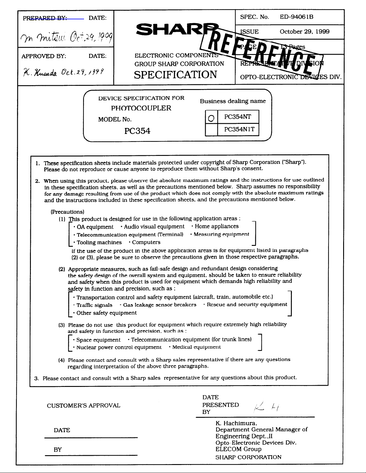
PREPARED BY:
DATE:
SPEC. No. ED-9466 1B
I
October 29. 1999
APPROVED BY: DATE:
DEVICE SPECIFICATION FOR
MODEL No.
I
SHA
ELECTRONIC COMPO
GROUP SHARP CORPORATION
SPECIFICATION
PHOTOCOUPLER
OF’TO-ELECT=
I
Business dealing name
I I
PC354
1. These speciilcation sheets include materials protected under copyright of Sharp Corporation (‘Sharp”).
Please do not reproduce or cause anyone to reproduce them without Sharp’s consent.
2. When using this product, please observe the absolute maximum ratings and the instructions for use outlined
in these specification sheets, as well as the precautions mentioned below. Sharp assumes no responsibility
for any damage resulting from use of the product which does not comply with the absolute maximum ratings
and the instructions included in these specification sheets, and the precautions mentioned below.
(Precautions)
(1) This product is designed for use in the following application areas :
l
l
OA equipment
. Telecommunication equipment (Terminal) * Measuring equipment
l
Tooling machines l Computers
1
If the use of the product in the above application areas is for equipment listed in paragraphs
(21 or (31, please be sure to observe the precautions given in those respective paragraphs.
(21 Appropriate measures, such as fail-safe design and redundant design considering
the safety design of the overall system and equipment, should be taken to ensure reliability
and safety when this product is used for equipment which demands high reliability and
safety in function and precision, such as ;
* Transportation control and safety equipment (aircraft, train, automobile etc.)
* Tram signals * Gas leakage sensor breakers * Rescue and security equipment
l
Other safety equipment
[
(31 Please do not use this product for equipment which require extremely high reliability
and safety in function and precision, such as :
* Space equipment * Telecommunication equipment (for trunk lines)
* Nuclear power control equipment * Medical equipment
[
(4) Please contact and consult with a Sharp sales representative if there are any questions
regarding interpretation of the above three paragraphs.
3. Please contact and consult with a Sharp sales representative for any questions about this product.
Audio visual equipment
* Home appliances
1
1
1
CUSTOMERS APPROVAL
DATE
BY
DATE
PRESENTED ;(i
BY
K. Hachimura.
Department General Manager of
Engineering Dept. ,I1
Opto-Electronic Devices Div.
ELECOM Group
SHARP CORPORATION
4
Page 2
SHARP CORPORATION
ED-94(
1. Application
This specification applies to the outline and characteristics of p
Model No. PC354.
2. Outline
Refer to the attached drawing No. CY6488KO2.
3. Ratings and characteristics
Refer to the attached sheet, page 4 to 6.
4. Reliability
Refer to the attached sheet, page 7.
5. Incoming inspection
Refer to the attached sheet, page 8.
6. Supplement
6.1 Isolation voltage shall be measured in the following method.
(1) Short between anode and cathode on the primary side and between
collector and emitter on the secondary side.
(2) The dielectric withstand tester with zero-cross circuit shall be used.
(3) The wave form of applied voltage shall be a sine wave.
6.2 Packaging specifications
Page 3
SHARPCORPORATION
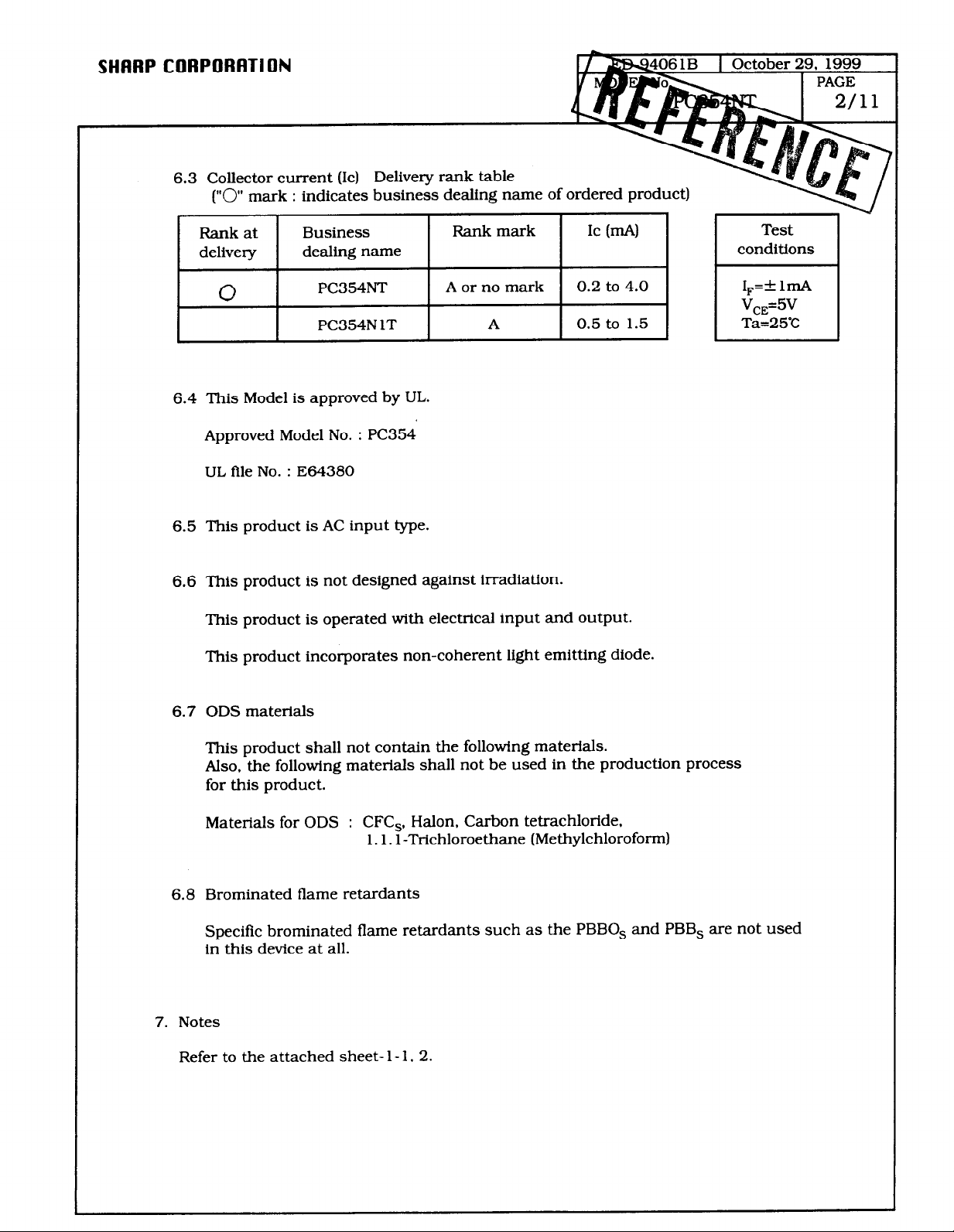
6.3 Collector current (Ic) Delivery rank table
(“0”
mark : indicates business dealing name of ordered product)
Rank at Business
delivery dealing name
8
6.4 This Model is approved by UL.
Approved Model No. : PC354
UL file No. : E64380
6.5 This product is AC input type.
6.6 This product is not designed against irradiation.
This product is operated with electrical input and output.
This product incorporates non-coherent light emitting diode.
PC354NT A or no mark 0.2 to 4.0
PC354N 1T A 0.5 to 1.5
Rank mark
Ic b-M
Test
conditions
I,=+ 1mA
V ca=5v
Ta=25C
6.7 ODS materials
This product shall not contain the following materials.
Also, the following materials shall not be used in the production process
for this product.
Materials for ODS : CFC,, Halon. Carbon tetrachloride.
1.1.1 -Trichloroethane (Methylchloroform)
6.8 Brominated flame retardants
Speciiic brominated flame retardants such as the PBBO, and PBB, are not used
in this device at all.
7. Notes
Refer to the attached sheet- 1- 1, 2.
Page 4
SHARP CORPORATION
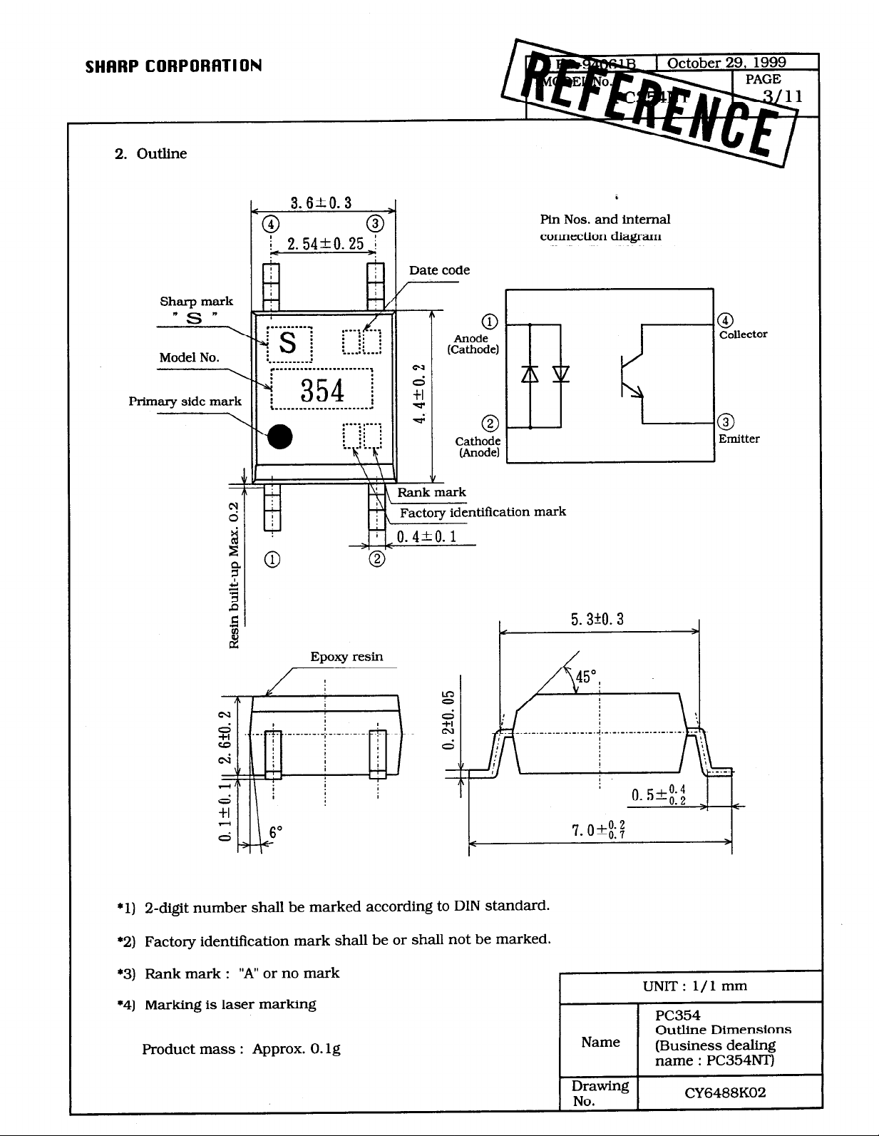
2. Outline
Sharp mark
“S”,
Model No.
\
Primary side mark
\
.
1
\,
. .
\*
c
3.6kO. 3
@
0
;
2.54kO.25
i
Date code
/
0
Anode
(Cathode)
d
&nk mark
0
Cathode
(Anode)
i
Pin Nos. and internal
connection diagram
Epoxy resin
+q=, g
4-L
6”
mark
3
Collector
3
Emitter
*l) 2-digit number shall be marked according to DIN standard.
*2) Factory identification mark shall be or shall not be marked.
*3) Rank mark : “A” or no mark
l
4) Marking is laser marking
Product mass : Approx. 0. lg
UNIT: l/l mm
Name
PC354
Outline Dimensions
(Business dealing
name : PC354NT)
Drawing
No.
CY6488KO2
L
Page 5
SHARP CORPORATION
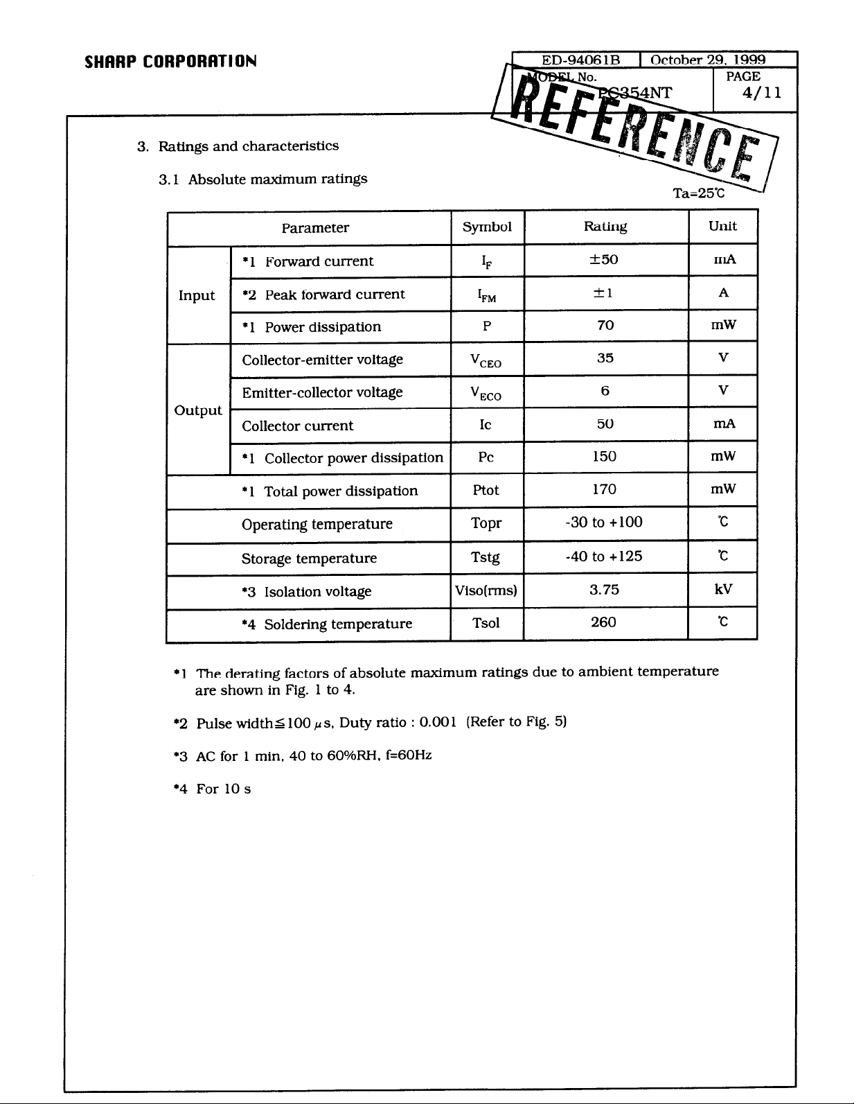
3. Ratings and characteristics
3.1 Absolute maximum ratings
Input
output
Collector current
* 1 Total power dissipation
Operating temperature Topr
Storage temperature Tstg
*3 Isolation voltage Viso(rms) 3.75
*4 Soldering temperature Tsol 260 %
* 1 The derating factors of absolute maximum ratings due to ambient temperature
are shown in Fig. 1 to 4.
*2 Pulse widths 100 /1 s. Duty ratio : 0.00 1 (Refer to Fig. 51
*3 AC for 1 min. 40 to 6O%RH, f=GOHz
*4 For 10s
-30 to +lOO ‘C
-40 to +125 “C
kV
Page 6

SHARP CORPORATION
3.2 Electra-optical characteristics
Input
output
Parameter Symbol Conditions MIN. m. MAX. uni;
Forward voltage
VF
1,=+2omA 1.2 1.4 v
Terminal capacitance Ct
v=o, f=lkHz
30 250 pF
Dark current
I,
EO
vc,=2ov, IF0 100 nA
Collector-emitter
BvCEO
Ic=O. 1 mA 35 - - V
breakdown voltage I,=0
Emitter-collector
BVECO
I,= 10 rA, I,=0 6 - - V
breakdown voltage
Collector current
IC
1,=+1mA, vc,=5v 0.2 - 4.0 mA
Collector-emitter
‘CE(sat)
1,=+2omA 0.1 0.2 v
saturation voltage
Ic=lmA
Transfer Isolation resistance Riso DCSOOV
5XlO’O 10” - Q
charac- 40 to 6O%RH
teristics
Floating capacitance Cf
V=O, f= 1 MHz 0.6 1.0 pF
Response time Rise tr VcE=2V
4 18 ps
’ Ic=2mA
Response time Fall tf Iq=lOOQ
3 18 ps
Page 7

SHARP CORPORATION
(Fig. 1) Forward current vs.
ambient temperature
-30 0 25 55 75 100 125
80
c
3 70
g 60
z
;ij
b
40
3
g 20
3
.2
n O
-30 0 25
100 125
Ambient temperature Ta (“C)
(Fig. 3) Collector power dissipation
vs. ambient temperature
-30 0 25 50 75 100 125
Ambient temperature Ta ("C)
(Fig. 5) Peak forward current
3
vs. duty ratio
Ambient temperature Ta (“C)
(Fig. 4) Total power dissipation
g 170
s 150
.9
2
100
;ij
F
Pulse widths 100 p s
Ta=25”C
-30 0 25 50 75 100 125
Ambient temperature Ta ("C)
vs. ambient temperature
a”
Duty ratio
Page 8

SHARP CORPOMTION
4. Reliability
The reliability of products shall satisfl
items listed below.
Test Items
Solderability *2
Soldering heat *3
Terminal strength
(Bending) *4
Mechanical shock
Variable frequency
vibration
Temperature
cycling
High temp. and high
humidity storage *5
23O’C. 5 s
26O’C. 10s
Weight : 1N
1 time/each terminal
150OOm/s*, 0.5ms
3 times/+X, +Y. +Z direction
100 to 2000 to lOOHz/4min
200m/s*
4 times/ X, Y. 2 direction
1 cycle -40°C to + 125’C
20 cycles test
+85-C. 85%RH. 500h
Test Conditions Failure Judgement
(30min) (30min)
Confidence level : 90%
LTPD : 100/o/20%
*1 Criteria
v,>ux 1.2
kEO>UX2
Ic<LX0.7
V
CE(sat)>ux 1.2
U : Upper
specification
limit
n=ll. C=O
n=ll, C=O
n=ll. C=O
n=ll. C=O
n=ll. C=O
n=22.C=0
n=22.C=0
‘I
High temp. storage +125-C. lOOOh
Low temp. storage -4O’C. lOOOh
Operation life
* 1 Test method, conforms to EIAJ ED 470 1.
*2 Solder shall adhere at the area of 95% or more of immersed portion of
lead, and pin hole or other holes shall not be concentrated on one portion.
l 3 The lead pin depth dipped into solder shall be 0.2mm away from the
root of lead pins.
*4 Terminal bending direction is shown below.
‘5 It in ~vall~at~rl after washing hv specified solvent in attach sheet- l- 1. 2.
1,=+5OmA. Ptot= 170mW
Ta=25’C, lOOOh
L : Lower n=22,C=O
specification
limit n=22.C=0
0.2mm or
n=22,C=O
H
more
+
Weight : 1N
Soldering a~
Page 9
SHARP CORPORATION
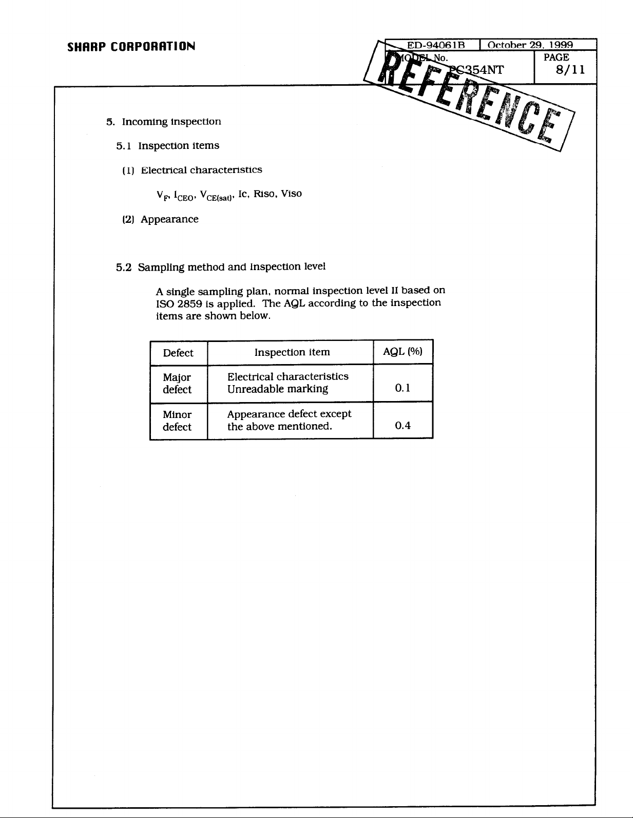
5. Incoming inspection
5.1 Inspection items
(1) Electrical characteristics
V,, I,,,, V,,(,,). Ic, Rise. Viso
(2) Appearance
5.2 Sampling method and Inspection level
A single sampling plan, normal inspection level II based on
IS0 2859 is applied. The AQL according to the inspection
items are shown below.
Defect
Major
defect
Minor
defect
Inspection item
Electrical characteristics
Unreadable marking
Appearance defect except
the above mentioned.
AQL (O/o)
0.1
0.4
Page 10

SHARP CORPORATION
6.2 Package specifications
6.2.1 Taping conditions
(1) Tape structure and Dimensions (Refer to the attached sheet, Page 10)
The tape shall have a structure in which a cover tape is sealed heat-pressed on
the carrier tape of protect against static electricity.
(2) Reel structure and Dimensions (Refer to the attached sheet, Page 11)
The taping reel shall be of plastic with its dimensions
as shown in the attached drawing.
(3) Direction of product insertion (Refer to the attached sheet, Page 11)
Product direction in carrier tape shall direct to the anode mark at the
hole side on the tape.
(4) Joint of tape
The cover tape and carrier tape in one reel shall be jointless.
(5) The way to repair taped failure devices
The way to repair taped failure devices cut a bottom of carrier tape with a cutter, and
after replacing to good devices, the cut portion shall be sealed with adhesive tape.
6.2.2 Adhesiveness of cover tape
. The exfoliation force between carrier tape and cover tape shall be
0.2N to 0.7N for the angle from 160’ to 180’ .
6.2.3 Rolling method and quantity
l
Wind the tape back on the reel so that the cover tape will be outside the tape.
Attach more than 20cm of blank tape to the trailer and the leader of the tape
and fur the both ends with adhesive tape. One reel shall contain 750~~s.
6.2.4 Marking
. The outer packaging case shall be marked with following information.
l
Model No.
* Number of pieces delivered l Production date
6.2.5 Storage condition
l
Taped products shall be stored at the temperature between
5 and 30°C and the humidities lower than 7O%RH.
6.2.6 Safety protection during shipping
l
There shall be no deformation of component or degradation of electrical
characteristics due to shipping.
Page 11

SHARP CORPORATION
Carrier tape structure and Dimensions
F I.-E I_
t
I- -I- i
D
5”
max
unit
\
Unit
\
Symbol
mm
Symbol
mm
A
12.0
F
4.0
f0.3
kO.1
B C
~
f0.05
5.5
G
+o. 1
-0.0
$J3 1.5
1.75
H
7.4
+o. 1
kO.1
D
kO.1
8.0
E
kO.05
2.0
-1
I J
-Lo.05 -to.1
0.3 3.1
-I-
K
kO.1
4.0
Page 12

SHARP CORPORATION
Reel structure and Dimensions
I
e
.
3
C
f
a
’ b
Check word
a b
C
d
I
e
I
f
I
g
I
mm 1 180 113.5S.51 8Okl.O 1 13f0.5 1 21fl.O 1 2.OkO.5 12.0f0.5 1
Direction of product insertion
Pull-out direction
Page 13

SHARP CORPORATION
Precautions for Photocouplers
1 For cleaning
(1) Solvent cleaning :
Solvent temperature 45C or less
Immersion for 3 min or less
(2) Ultrasonic cleaning : The effect to device by ultrasonic cleaning differs
by cleaning bath size, ultrasonic power
output, cleaning time, PCB size or device mounting
condition etc. Please test it in actual using condition
and confirm that doesn’t occur any defect before starting
the ultrasonic cleaning.
(3) Applicable solvent :
Ethyl alcohol, Methyl alcohol, Isopropyl alcohol
In case when the other solvent is used, there are cases that
the packaging resin is eroded. Please use the other solvent
aiter thorough confirmation is performed in actual using condition.
2. The LED used in the Photocoupler generally decreases the light emission power
by operation.
In case of long operation time, please design the circuit with considering
the degradation of the light emission power of the LED. (50%/5years)
3. There are cases that the deviation of the CTR and the degradation of the light emission power
of the LED become big at IF is less than l.OmA.
Please design the circuit with considering this point.
Page 14

SHARP CORPORATION
4. Precautions for Soldering Photocouplers
(1) If solder reflow :
It is recommended that only one soldering be done at the temperature
and the time within the temperature profile as shown in the figure below.
h-9406 11
25°C
amin
<
+I+
30 s
lmin
1.5 min
lmin
<
>
Since, influence to the device is different according to reflow equipment
and its condition, please use the device after confirming no damage
in the actual using condition.
(2) Other precautions
An infrared lamp used to heat up for soldering may cause a localized
temperature rise in the resin. So keep the package temperature within
that specified in Item (1). Also avoid immersing the resin part in the solder.
 Loading...