

Page 1

DVD Video Player
SERVICE MANUAL
MODELS
DV-SV92S(Y,RU,B,U)
In the interests of user-safety (Required
by safety regulations in some
countries) the set should be restored to
its original condition and only parts
identical to those specified be used.
CONTENTS
1. GENERAL DESCRIPTION................................................................................................................2
1.1. ES6809 Vibratto-II CL DVD Processor......................................................................................2
1.2. Memory......................................................................................................................................3
1.3. Front Panel................................................................................................................................3
1.4. Back Panel.................................................................................................................................3
2. SYSTEM BLOCK DIAGRAM and ES6809 PIN DESCRIPTION.......................................................4
3. AUDIO INTERFACE..........................................................................................................................8
4. AUDIO PERFORMANCE..................................................................................................................8
5. VIDEO INTERFACE..........................................................................................................................8
6. SDRAM MEMORY............................................................................................................................9
7. FLASH MEMORY..............................................................................................................................9
8. SERIAL EEPROM MEMORY............................................................................................................9
9. DIGITAL SERVO CONTROLLER....................................................................................................10
10. FRONT PANEL........................................................................... .....................................................10
11. RESET CIRCUITRY & VOLTAGE REGULATORS..........................................................................10
12. CONNECTORS........................................... .....................................................................................11
12.1 Loader Connectors..................................................................................................................11
12.2 Scart Connector......................................................................................................................12
13. CIRCUIT DESCRIPTION.......................................... .......................................................................13
13.1 Power Supply...........................................................................................................................13
13.2 Front Panel...............................................................................................................................14
CD UPDATE PROCEDURE OF DV-SV92.............................................................................................14
CIRCUIT SCHEMATICS.........................................................................................................................28
SHARP CORPORATION
Page 2

1. GENERAL DESCRIPTION
1.1 ES6809 Vibratto-II CL DVD Processor
DESCRIPTION
The ES6809 Vibratto™II CL processor is a single chip DVD system on chip with DivX®, MPEG-4,
and DVD video playback. The ES6809 integrates all front-end DVD servo control functions
including read channel, ECC, servo DSP, MCU for high performance disc read and a high quality
TV encoder for a brilliant 480p/576p progressive scan video output with Macrovision™ copy
protection. The ES6809 is an ideal solution for stand-alone DVD players, DVD receivers,
DVD/VCR combos and DVD A/V minicomponent s ystems.
The ES6809 is built on the ESS proprietary dual CPU Programmable Multimedia Processor
(PMP) core consisting of 32-bit RISC and 64-bit DSP processors that deliver the best DVD
feature set. This PMP core, common through out all generations of Vibratto DVD pr oducts,
allows for easy migration from previous ESS based designs. The processing units enable
simultaneous parallel execution of system commands and data processing to per form specialized
encoding and decoding tasks. The vector engine performs audio and video processing to support
MPEG, Dolby®, DTS™, JPEG and DivX standards.
The front-end servo control of the ES6809 supports all popular optical pick-up units (OPU). Its
high performance error handling allows for playback of scratched and fingerprinted media. The
ES6809 has a unified memory architecture for both the front-end servo control and backend
decoder to achieve the lowest possible system memory cost.
The ES6809 has unmatched audio features including an integrated high quality stereo audio
digital to analog converter (DAC) and an analog to digital converter (ADC).
Additionally, the ES6809 supports DVD-Audio, CD-DA, HDCD, MP3, WMA, AAC, Dolby
ProLogic™ II digital audio formats and Karaoke.
The ES6809 CL DVD processor with DTS support is offered with the ES6809D, which has the
same pinout as the standard ES6809. The ES6809 and ES6809D processors are in 208-pin
Plastic Quad Flat Pack (PQFP) device package.
FEATURES
•
DVD SoC incorporating all front-end DVD servo control and back-end DVD decode.
• DivX Home Theater quality video at full screen (D1).
• MPEG-4 Advanced Simple Profile* video.
• DVD-Audio multi-channel playbac k including MLP and 24-bit LPCM decode, CPPM decryption
and watermark detection
• DVD-Video, DVD-R/RW, DVD+R/RW, SVCD, VCD, CDROM, CD-R/RW, CD-DA.
• High-performance focusing, sledding, tracking and CLV/CAV spindle s erv o control.
• Integrated stereo audio DAC and audio ADC.
• Integrated NTSC/PAL encoder with pixel-adaptive deinterlacer
• Five 54 MHz VDACs for simultaneous c omposite, Sv ideo and YUV video outputs.
• Macrovision NTSC/PAL interlaced and progressive scan (480p/576p) video output
• Direct interface of 16-bit DRAM with up to 128-Mb capacity
• Direct interface for up to 4 banks of 8-bit EPROM or Flash memory with up to 4 MB per bank
• CCIR656/601 YUV 4:2:2 input/output
• OSD controller supports 256 colors in 8 degrees of transparency
• Sub-picture Unit (SPU) decoder supports karaoke lyric, subtitles and EIA-608 compliant Line 21
captioning.
• Dolby Digital, Dolby ProLogic, and Dolby ProLogic II
• DTS Digital Out
2
Page 3

• SRS TruSurround®
• MPEG Multichannel, AAC, MP3.
• SPDIF digital audio input and output
• JPEG digital photo support (Kodak Picture CD™ and Fujifilm FujiColor CD™)
1.2 MEMORY
1.2.1 System SRAM Inte r fa c e
The system SRAM interface controls access to optional external SRAM, which can be
used for RISC code, stack, and data. The SRAM bus support s four independent address spaces,
each having programmable bus width and wait states. The interface can support not only SRAM,
ROM/EPROM and memory-mapped I/ O port s for standalone applications are also supported.
1.2.2 DRAM Memory Interface
The Vibratto-II CL provides a glueless 16-b it int erfac e to DRAM memor y devices us ed as
video memory for a DVD player. The maximum amount of memory supported is 16 MB of
Synchronous DRAM (SDRAM). The memory interf ace is conf igurable in depth to support 128-Mb
addressing. The memory interface controls acc ess to both external SDRAM or EDO memories,
which c an be th e sol e un ifi ed e xt er nal rea d/ writ e m em or y ac ti ng as prog ra m an d da ta mem or y as
well as various decoding and display buffers.
1.3 F
RONT PANEL
The front panel is based around an VFD and a common NEC (or compatible) front panel
controller chip, (uPD16311). The chipset ES6809 controls t he uPD16311 using several control
signals, (clock, data, chip select). The infrared remote control signal is passed directly to the
ES6809 for decoding.
1.4 Back PANEL
A typical rear panel is included in the reference design. This rear panel supports:
- Two channel audio outputs
- Optical and coax S/PDIF outputs.
- Composite, SCART outputs
The six-video signals used to provide CVBS and RGB are generated by the ES6809’s
internal video DAC. The video signals are buffered by external circuitry.
3
Page 4
2. SYSTEM BLOCK DIAGRAM and ES6809 PIN DESCRIPTION
4
Page 5

ES6809 PIN DESCR I PT I O N
Names
1, 11, 20, 36, 45, 53, 63, 80,
VD33
AUX0
AUX3
RESET#
AUX1
DMA11:0
VSS
DRAS2-0#
DCS1-0#
VDD
DCAS#
DOE#
DW E #
DSCK
DQM
DB15-0
LA21-0
LWRLL#
LCS3-0#
LD7-0
LOE#
SPDIF_O U T
SPDIF_IN
VD33PLL
VS33PL L
VREF
COMP
RSET
FDAC
VDAC
VD33_D A
VS33_DA
YDAC
CDAC
UDAC
ADC_BIAS
MIC
ADC_CA P
TW S
TSD0
TSD1
Pin Numbers I/O Definitions
97, 122, 130, 156, 182, 197
2 I/O Host control 0.
3 I/O Auxiliary port 3.
4 I Reset (active-low).
5 I/O Host control 1.
6:9, 12:18, 21 O DRAM address bus.
10, 19, 27, 35, 44, 52, 62,
72, 79, 87, 96, 123, 133,
138, 183, 196, 201, 208
22, 23, 26 O DRAM row address strobes (active-low).
24, 25 O DRAM chip selects (active-low).
28, 73, 88, 134, 202 P Core power supply.
29 O DRAM column address strobe (active-low).
30 O DRAM output enable (active-low).
31 O DRAM write enable (active-low).
32 O Output clock to DRAM.
33 O Data input/output mask.
34, 37:43, 46:51, 54, 55 I/O DRAM data bus.
56:61, 64:67, 69:71, 74:78,
81:83, 101
68 O SRAM bus write enable (active-low).
84:86, 89 O SRAM bus chip select (active-low).
90:95, 98, 99 I/O SRAM data bus.
100 O RISC port output enable (active-low).
102 O S/PDIF output.
103 I S/PDIF input.
104 P Power for PLL blocks.
105 G Ground for PLL blocks.
106 I Internal voltage reference to video DAC.
107 I Compensation input.
108 I DAC current adjustment resistor input.
109 O Video DAC output .
110 O Video DAC output.
111 P Power for I/O power supply for VDAC.
112 G Ground for I/O power supply for VDAC.
113 O Video DAC output .
114 O Video DAC output .
115 O Video DAC output .
116 O Audio ADC bias voltage out.
117 I Audio ADC MIC 1.
118 O Audio ADC output capacitance.
119 O Audio transmit frame sync output.
120 O Audio transmit serial data port 0.
121 O Audio transmit serial data port 1.
P I/O power supply.
G Ground.
O SRAM address bus.
5
Page 6

TSD2
TSD3
TBCK
TXD0
RXD0
MCLK
TXD1
RXD1
AUX3[5]
AUX3[0]
TX
RX
LDCO
LG
IP2
SDEN
SDATA
SCLK
DFCT
MIRR
LDON
BSUM
FE
CE
TE
RFENV
VREFOUT
VREFIN
DMO
FOO
SLO
RPBC
TRO
NC
TEBC
REFD
IN_M
IN
AVDD3
AVSS
DVCC
IP1
IDSEL
AMPSTB Y
FGIN
CLOSESW
HOMESW
CLOSE
124 O Audio transmit serial data port 2.
125 O Audio transmit serial data port 3.
126 O Audio transmit bit clock.
127 I/O Serial port 0 transmit.
128 I/O Serial port 0 receive.
129 I/O Audio master clock for audio DAC.
131 I/O Serial port 1 transmit.
132 I/O Serial port 1 receive.
135 I/O Aux3 data I/O 5.
136 I/O Aux3 data I/O 0.
137 I Zero crossing of TE.
139 I Zero crossing of RF envelope.
140 O CD/DVD laser diode select.
141 O DVD-RAM land/groove flag for next track.
142 I DVD-RAM header position index 2.
143 O RF chip serial data enable.
144 I/O Data signal to/from RF chip.
145 O Serial clock source to RF chip.
146 I Defect flag input signal.
147 I Mirror detect input.
148 O Laser diode on/off control.
149 I Photodiode subbeam addition input s ignal.
150 I Focus input error signal.
151 I Center error input signal.
152 I Tracking error input.
153 I RF ripple envelope input signal.
154 I
155 I Reference voltage for servo analog input signals.
159 O Spindle drive.
160 O Focus drive.
161 O Sled drive.
162 O RF envelope balance control.
163 O Track drive.
164 O No connect.
165 O Track ing error balance control.
166 I Flash reference decouple.
167 I Analog RF signal (minus).
168 I Analog RF signal (plus).
169 P 3.3V analog power for flash.
170 G Analog ground for flash.
171 P 1.8V power for flash.
172 I DVD-RAM header position index 1.
173 I/O DVD-RAM detected signal of ID area.
174 O Power amplifier standby.
175 I Spindle hall sensor input.
176 I Tray closed detector.
177 I Sled home switch position detector.
178 O Drive t o close tray.
Reference voltage for servo analog output
signals.
6
Page 7
OPENSW
OPEN
MDET
AUX7
AUX3[7]
EAUX1
AUX3[6]
EAUX0
EAUX3
EAUX2
VSYNC#
HSYNC#
XI
XO
AUX3[4]
AUX3[1]
AUX3[3]
AUX3[2]
AUX6-4, 2
179 I Tray open detector.
180 O Drive to open tray.
181 I Spindle drive motor rot ation direction detect.
184 I/O Auxiliary port 7.
185 I/O Aux3 data I/O 7.
186 I/O Extended auxi liary port 1.
187 I/O Aux3 data I/O 6.
188 I/O Extended auxi liary port 0.
189 I/O Extended auxi liary port 3.
190 I/O Extended auxi liary port 2.
191 I/O Vertical sync (active-low); (5V tolerant input).
192 I/O Horizontal sync (active-low); (5V tolerant input).
193 I Crystal clock in.
194 O Crystal clock out.
198 I/O Aux3 data I/O 4.
199 I/O Aux3 data I/O 1.
200 I/O Aux3 data I/O 3.
203 I/O Aux3 data I/O 2.
204-207 I/O Auxiliary ports 2, 4, 5 and 6; (5V tolerant input).
7
Page 8

3. Audio Interface
The audio interface is a bidirectional serial port that connects to an external audio ADC/DAC for
the transfer of PCM (pulse coded modulation) audio data in I
2S format. It supports 16-, 24-, and
32-bit audio frames. No external master clock is required.
The ES6809 offers three audio interface modes:
1. Stereo mode using TSD0 pin 120.
2. Dolby Digital (AC-3) 5.1 channel mode using TSD[3:0] pins 120, 121, 124, and 125.
3. Dolby Digital (AC-3) 5.1 channe l mode using S/PDIF pins 102 and 103.
4. Audio Perform an c e
Table 36 lists the audio performance characteristics of the digital audio processor of the ES6809
under normal operating conditions (AVCC = 3. 3V ±10%, DVCC =2.5±10%, TAMB 0 to 70°C).
Parameter Typical Unit
ADC Resolution 16 Bit
ADC Data Sample Rate 192 KHz
ADC Dynamic Range 80 dB
ADC THD 1 %
DAC Resolution 24 Bit
DAC Sample Rate 192 KHz
DAC THD+Noise 75 dB
DAC Dynamic Range 88 dB
DAC Bandwidth 20 KHz
5 VIDEO INTERFACE
Video Displa y Output
The video output section controls t he transfer of video frames stored in mem ory to the internal TV
encoder of the Vibratto. The output sec t ion consists of a programmable CRT controller capable of
operating either in Master or Slave mode.
The video output section features internal l ine buffers which allow the outgoing lumin ance and
chrominance data to match the internal clock rates with external pixel clock rates, easily
facilitating YUV4: 2:2 to YUV4: 2:0 component and sample conversion. A polyphase filter
achieves arbitrary horizontal decimation and interpolation.
Video Bus
The video bus has 8 YUV data pins that transfer luminance and chrominance (YUV) pixels in
CCIR601 pixel format (4:2:2). In this format, there are half as many chrominance (U or V) pixels
per line as luminance (Y) pixels; there are as many chrominance lines as luminance.
Video Post-Proce s sing
The Vibratto video post-processing circuitry provides support for the color conversion, scaling,
and filtering functions through a combination of special hardware and software. Horizontal upsampling and filtering is done with a programmable, 7-tap polyphase filter bank for accurate
non-integer interpolations. Vertical scaling is achieved by repeating and dropping lines in
accordance with the applicable scaling ratio.
8
Page 9
Vide o Timi ng
The video bus can be clocked either by d ouble pixel clock and cl ock qualifier or by a single pixel
clock. The double clock typically is used for TV displays, the single for computer displays.
6 SDRAM MEMORY
The ES6809 provides a glueless 16-bit interface to DRAM memory devices used as video
memory for a DVD player. The maximum amount of memory supported is 16 MB of
Synchronous DRAM (DRAM). The memory interface is configurable in de pth to support 128-Mb
addressing.
Typical SDRAM Configurations:
The memory interface
controls access to both external
SDRAM or EDO memories, which
can be the sole unified external
read/write memory acting as
program and data memory as well
as various decoding and display
buffers. At high clock speeds, the
Vibratto memory bus interface
has sufficient bandwidth to support
the decoding and displaying of
CCIR601 resolution images at full
frame rate.
7 FLASH M
The decoder board supports AMD class Flash memories. Currently 4 configurations are
supported:
FLASH_512K_8b
FLASH_1024K_8b
FLASH_512Kx2_8b
FLASH_512Kx2_16b
The Vibratto permits both 8- and 16-bit common memor y I/O accesses with a removable storage
card via the host interface.
EMORY
ERIAL EEPROM MEMORY
8 S
An I2C serial EEPROM is used to store user configuration (i.e. language preferences,
speaker setup, etc.) and software configuration.. Industry standard EEPROM range in size from
1kbit to 256kbit and share the same IC footprint and pinout. The def ault device is 2kbit, 256kx 8,
SOIC8 SGS Thomson ST24C02M1 or equivalent.
9
Page 10
9 Digital Servo Controller
The digital servo includes an internal
DSP, on-chip RAM and ROM, control
logic, a loader interface, a serial
interface, and an on-chip ADC-DAC,
and interfaces with the MCU.
The MCU handles the high-level
functions of optical disk and front-end
system control. The interface between
the servo controller and the MCU is
illustrated in the Figure.
10 FRONT PANEL
VFD C
include a simple state machine which sc ans the VFD and reads the front panel button m at rix. T he
16311 also includes RAM so it can s tore the current state of all the VFD icons and segments.
Therefore, the 16311 need only be accessed when the VFD status changes and when the button
status is read. The ES6809 can control this chip directly using PIO pins or can allo w the front
panel PIC to control the VFD.
ONTROLLER
The VFD controller is a NEC uPD16311. This controller is not a processor, but does
11 RESET CIRCUITRY & VOLTAGE REGULATORS
Two different chips are supported to provide the power-on-reset AAT3521 or AAT3520.
Voltage regulators:
U6: LM1117(1.8V) For 2V PLL power supply
U19: 7805 For 5V power supply
10
Page 11
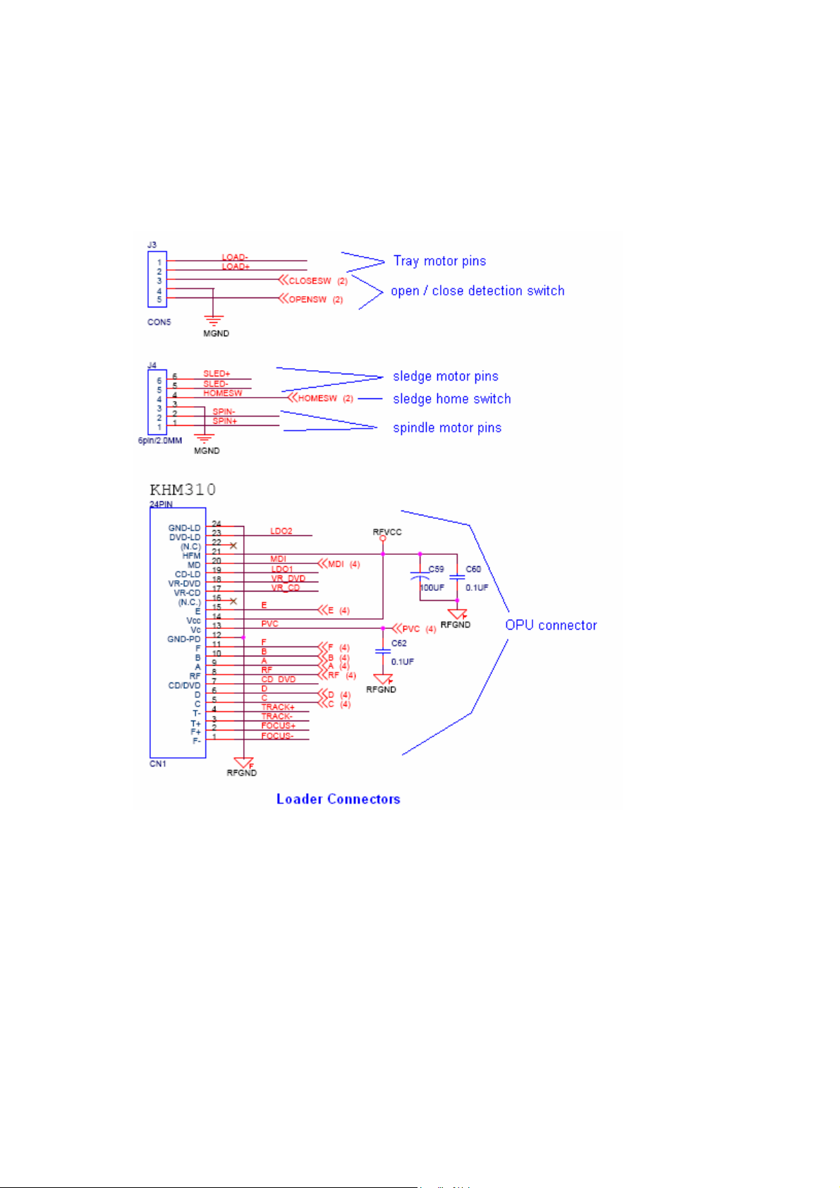
12 CONNECTORS
S75 DL3CH
12.1 LOADER
CONNECTORS:
11
Page 12

12.2 SCART CONNECTOR
Some cheaper SCART cabl es use unshielded wires, which is just about acceptable for
short cable lengths. For longer lengths, shielded co-ax cable become essential.
Scart Signals:
Audio signals
0.5V RMS, <1K output impedance, >10K input impedance.
Red, Green, Blue
0.7Vpp ±2dB, 75R input and output impedance. Note that the Red connection (pin 20) can
alternatively carry the S-VHS Chrominance signal, which is 0.3V.
Composite Video / CSync
1Vpp including syn c, ±2dB, 75R input and output impedance.B andwidth = 25Hz to 4.8MHz for
normal TV Video de-emphasis to CCIR 405.1 (625-line TV)
Fast Blanking
75R input and output impedance. This control voltage allows devices to over-ride the composite
video input with RGB inputs, for example when inserting closed caption text. It is called fast
because this can be done at the same speeds as other video signals, which is why it requires the
same 75R impedances.
12
Page 13

0 to 0.4V: TV is driven by the composite video input signal (pin 19).
Left unconnected, it is pulled to 0V by its 75R termination.
1V to 3V: the TV is driven by the signals Red, Green, Blue and composite sync. The
latter is sent to the TV on pin 19. This signal is useful when using a TV to display the
RGB output of devices such as home computers with TV-compatible frame rates. Tying
the signal to 5V via 100R forms a potential divid er with the 75R terminati on, holding t he
signal at around 2V. Alternatively, if a TTL level (0 to 5V) negative sync pulse is
available, this will be high during the display periods, so this can drive the blanking signal
via a suitable resistor.
Control Voltage
0 to 2V = TV, Normal.
5 to 8V = TV wide screen
9.5 to 12V = AV mode
13. CIRCUIT DESCRIPTION
13.1 POWER SUPPLY:
o Socket PL2 is the 220VAC input.
o 2.5A fuse F1 is used to protect the device against short circuit and
unexpected overloads.
o Voltage is rectified by using D1-D2-D3-D4 diodes. Using capacitor
C33,C34 (47∝f) a DC voltage is produced. (310- 320VDC).
o The current in the primary side of the transformer TR2 comes to the
SMPS IC (TNY267P). It has a built-in oscillator, overcurrent and
overvol tage pro tection ci rcuitr y. It starts with the c urrent f rom the p rimary
side of the transformer and fol l o ws t h e cu rrent fr om the feed b a ck windin g.
o Feedback current is deteceted by optocoupler IC2. Depending on the
control current coming from the secondary side, SMPS IC keeps the
output voltage constant by controlling the duty cycle of the PWM at the
primary side of the transformer.
o Voltages on the secondary side are as follows: +12 Volts at D20, +5
Volt s at D12, +3.3V at D13, -22V D1 9, Using t he output of the D25, a
photo diode inside of the IC2 generates feedback signal bu using
optocoupler's photo transistor. This photo transistor adjusts the control
voltage at the IC3. The voltage at this pin effects the pwm output
frequency on the IC3 pin5 (Drain pin). And finally output voltages reach
their correct values by this way.
o –22 Volts is used to feed the VFD (Vacuum Fluorescent Display) driv er IC
on the front panel.
13
Page 14

13.2 FRONT PA N EL:
o All the functions on the front panel are controlled by ES6809 on the
mainboard. Key scanning and IR checking operations on the standby mode
are controlled by VFD driver IC (uPD16311).
o ES6809 IC sends the commands to uPD16311 via socket J2 (pins 2,3 and 4).
o There are 16 keys scanning function, 2 LED outputs, 1 Stand-by output and
VFD drivers on the uPD16311 IC.
o Front panel LED is bright red i n stand-by mode a nd green whe n the device is
turned on.
o IR remote control receiver module (TSOP1836) sends the commands from
the remote control directly to the ES6809.
CD Update Procedure of DV-SV92
1. Download the update file from the convenient link according to your default
language choice.
2. While there is no CD in the DVD (No Disc Mode) , press “Menu 1 3 5 7”
buttons on the remote control in order to reach the Service Menu of DVD
Player:
2.1. Note the software version described as “b.xx “ to be able to compare the
sw. Version after update process.
3. Copy the update file to the desktop and rename it according to the update file
name in the hidden menu of the device.
For example If M2101RP_ is written then rename it like M2101RP_.rom
If S6111___ is written then rename it like S6111___.rom
(If you receive the update file already renamed (with addition of .rom) from the
customer technical support department by giving the SAP code of the product
then burn the already renamed file with nero program as it is shown below.)
14
Page 15

4. Burn the renamed files by Nero program with below set up.
5. After burning process is completed, place the update CD into the DVD tray
and press play button.
6. Wait to see the update process steps as shown below. When the sw. Update
is completed unit will switch itself to standb y mode.
7. Finally, press the eject button and take out the update CD while DVD Player
remains at stand by Mode.
8. Updating process has been completed. To check whether it is updated
correctly or not, repeat the first step for comparing software version
9. If the previous and letter names are different, CD is update has completed
successfully. If the name remains same than go through the steps from the
beginning.
IMPORTANT NOTE: If the AC source breaks down while the updating the
unit (main board) will be totally out of order. This kind of units/boards is out
of Warranty.
15
Page 16

Brief Information of Naming the File
Software version differs from each other depending on front models, loader type
etc. Each character in the file name is an abbreviation of a description as
illustrated below.
M 2 1 0 1 R P W
W M A Option (with WMA : W, without WMA: _ )
Progressive option (with progressive: P, without progressive:_ )
DMR option (with DMR:R, without DMR:_ )
DivX Subtitle Codepage
OSD Language Bank
Front Panel ( 1: 6311 FP , 2: 6312 FP )
Channel (2, 6)
Loader Type ( S: Sony KHM 310 , K: Sony KHM 313 , M:
Samsung S75 )
16
Page 17

Pay attention the le ft side. Select CD and CD_ROM (ISO) on the upper left side of screen
17
Page 18

Select No Multisession
18
Page 19

Format is Mode 1
19
Page 20

20
Page 21

Leave the dates as it is
21
Page 22

Leav e it as it is
22
Page 23

Click the “New” on the upper right corner of the screen
23
Page 24

Select your file from file browser then you will see your file in the “Name” section on the right side and
then copy the files to under “Name” section on the left side.(this is just an example you will see your file
name when you are doing this process)
24
Page 25

Click the “Burns the current compilation”
25
Page 26

Then you will see this screen and click the “Burn” on the right upper side of screen
26
Page 27

You will see this screen and tray will open itself on computer ,then place the CD in CD-ROM
And it will start writing. At the end you will see “burn complited”
27
Page 28

A5
of
15Wednesday, June 29, 2005
1
ESS TECHNOLOGY, INC.
2
Title
VESTEL-4500
INDEX
Size Document Number Rev
1
Date: Sheet
2
Revision History
Rev-A1
Base on ESS NEO-A8
Rev-A2
1.Delete P9.
2.Change P1 package net.
1.Change (U2.12),(U7.1),net to RESET#.
Rev-A3
Rev-A4
1.Reset IC power for 3.3V to 5V
2.added Capacities C22 -23,C26-29.
Rev-A5
3
4
Layout---------VESTEL-4500-A4B4
VESTEL-4500 ES68xx + KHM310/DL3CH + OUTPUT
1.Added Resistor R20,R32.
SCARTCTL0
FUNCTION
SCARTCTL1
01
AUXxx
RXD1
ate_en
SCARTCTL2
03
02
TXD000SPARE
TXD1
15
14 RXD0
133212
HSYNC
VSYNC
17
16
SPARE/VFDCLK
SPARE
31
SPARE
SPARE30SPARE
SPARE
35
34
33
36
SPARE
37
3
4
RAM
ROM/FLASH
LCS3#
B B
FUNCTION
I2C DATA
AUXx
AUX0
FUNCTION
Single chip processor that handles all system control, DVD decoding and servo control.
System setup configuration storage
Data storage and frame buffer using either 1 pc of 4Mx16 SDRAM or 2 pcs of 1Mx16 SDRAM
Program storage using either 4Mbit Flash or 8Mbit Flash
5
CHIP
32/64MBit SDRAM
24C01 SERIAL EE
ES68xx
Background
This DVD design is based on ESS ES68xx single chip DVD mpeg and servo processor. The ES68xx is buil t upon ESS
proven Programmable Multimedia Processor architecture with integrated servo DSP. A comple te DVD design using
ES6603 RF-Amp can support all major popular optical pickup heads. With ES68xx unify memory architecture, the whole
D D
System Clock Requirement
andy_ho@esstech.com.hk
system memory is reduced to a minimum. ES68xx provides the best pr ice performance DVD solution in the industry and
include the latest MPEG4/DivX playback capability.
ES68xx require a 27MHz clock to operate. This 27MHz can either b e generated externally and feed into pin 193 and pin
195 or thru a 27MHz crystal attached to pin 193 and 19 4. This 27Mhz will be used for all video processing reference. In
addition, internal multiplier will generate a much higher operatin g frequency for the internal RISC+DSP code to operate.
Audio clock is generated from ES68xx by its internal PLL circuitry.
SDRAM Usage
ES68xx supports different SDRAM configuration from 1Mx16, 4Mx16 to 8Mx16 S DRAM. The basic requirement can go as
System Configuration
low to 2 pcs of 1Mx16 SDRAM with standard feature set. You can also ma ke use of 8Mx16 SDRAM to achieve longer ESP
antishock time for portable application.
C C
4/8Mbit EPROM/FLASH
FUNCTION
LCSx#
LCS0#
FLASH
I/O expand
LCS2#
LCS1#
I2C CLOCK
VFD DATA
AUX1
AUX2
IR/SPARE
AUDIO BUFFER CONTROL
AUX3
AUX4
AMP_PWR/DFCT
AUX5
VFD CS#
AUX6
VFD CLK/IR
EXPANSION I/O
AUX7
SPARE
SPARE
FUNCTION
1
0
XAUXx
SPARE
SPARE
2
3
SPARE
4
A A
SPARE
SPARE
5
6
5
7 SPARE
Page 29

C156
0.1UF
0AAT3521
OPEN
0
R19 100K
OPEN
VCC
AAT3520
U3
R265
C16
GNDA GNDA
UDAC (5)
PWM_01L
UDAC
CDAC
PLL0 PWM_02L
ADC_CAP
PLL2
ADC_BIAS
114
115
116
117
118
119
120
121
MIC
UDAC
ADC_CAP
ADC_BIAS
TWS/PWM_O1L/PLL2
TSD0/PWM_O2L/PLL0
TSD1/PWM_O2R/PLL1
VD33
DB[6]
DB[5]
DB[4]
DB[3]
DB[2]
DB[1]
DB2
DB5
DB1
DB4
DB0
DB3
DB6
GND
4Mx16 SDRAM (9ns)
32/64MBIT SDRAM
R35 open(4.7K)
GND
MB2DB2
MB1
MB0DB0
DB1
RESET#
R37
12345
RESET
1.8K
0.1UF
CDAC (5)
YDAC (5)
YDAC
GNDV
112
113
YDAC
CDAC
DB[0]
VSS
GND
VD33
MB4DB4
DB3 MB3
OPEN\0
R36
OPEN\0
EN
NC
VCC
GND
GNDA
C17
VDAC (5)
5DAC (5)
VDAC
VD33DAC
RSET
108
109
110
111
FDAC
VDAC
VS33DAC
VD33DAC
VD33
DB[8]
DB[9]
DB[10]
DB9
DB10
DB11
DB8
CLOSE
OPEN
RA7RA5
OPEN
CLOSE
RA6
OPEN
OPENOPEN
OPEN
OPEN
RA4
OPEN OPEN
OPEN
OPEN
OPEN
RA3
CLOSE OPEN
CLOSE
CLOSE
OPEN
RA2
RA1
OPEN
64M SDRAM CLOSE
32M SDRAM BA0=1
32M SDRAM BA0=0
MB6DB6
MB5DB5
DB8 MB8
DB7 MB7
123
VCC
GND
RESET
U18
AAT3521 SOT-23(5pin)
0.1UF
GND
COMP
VREF
105
106
107
VREF
RSET
COMP
VS33PLL
DB[11]
DB[12]
DB[13]
VSS
DB12
DB13
GND
OPEN
OPEN
OPEN
OPEN
CLOSE
CLOSE32M SDRAM BA1=1 OPEN
OPEN
OPEN
OPEN
OPEN
CLOSE OPEN
CLOSE
32M SDRAM BA1=0
MB12DB12
MB14DB14
MB10DB10
MB9DB9
DB11 MB11
DB13 MB13
2 2
AAT3520 SOT-23(3pin)
DB15 MB15
C165
0.1UF
0.1UF
C164
0.1UF
C163
C162
0.1UF
0.1UF
C161
C160
0.1UF
0.1UF
0.1UF
R60
4.7K
DCLK INPUT
C186
10UF
C185
0.1UF
C184
0.1UF
C183
0.1UF
C182
0.1UF
C181
0.1UF
C180
0.1UF
LD5
LD7
LD6
LD4
21
D7
272623
LA7
LA8
LA6
LA4
LA10
LA9
LA5
LA0
LD5
LD6
LD7
DQ5
DQ6
DQ7
DQ13
DQ14
DQ15/A_1
A12
A11
A10A9A8NCNC
101112131415161718192021222324 25
LA20
LA11
LA12
LA21
LA13
LA9
LA10
VCC33 VDD2V
25428
LA11
LD4
DQ12
WRLL#
0.1UF
0.1UF
0.1UF
0.1UF
10UF
10UF
GND
GND
SDRAM, FLASH, ETC.
A11
LA12
DQ4
W
RESET#
VCC
A12
A13
29
LA13
LA14
LD3
VCC
DQ11
RP
VPP
C155
ES6620
GNDA
GNDVGNDV
VD33
VD33PLL
PLL3
LA1
LOE#
LD0
LD1
VD33
GND
LD2
LD3
LD4
LD5
LD6
LD7
LCS3#
VDD2V
GND
LCS2#
LA0
LA17
LA2
VD33
GND
LA3
LA4
LA5
LA6
LA7
VDD2V
GND
LA8
LA18
LA19
WRLL#
LA21
LA20
LA9
LA10
VD33
GND
LA11
LA12
LA13
LA14
LA15
LA16
DB15
DB14
VD33
LD0
13141517181920
U4
D0D1D2D3D4D5D6
A0A1A2A3A4A5A6A7A8A9A10
121110
LA1 LD1
LA0
LA17
R63 OPEN
R64 0
U2
123456789
VCC
VCC33
LA16
A16
A15
PLL3
VCC33
LD2
LA2
BYTE
A14
LA15
C154
C153
C152
C151
C150
C149
C89
SPDIF_OUT (5)
CRYSTAL OSC1CLK SOURCE
0
OSC, RESET, TTL, PLL
LD3
98765
LA3
GND
A13
LA14
GND
C21 0.047UF
R62 360 OHM 1%
C20 0.1UF
VD33PLL
104
SPDIF
103
SPD_DOBM/PLL3
102
LA[1]
101
LOE#
100
LD[0]
99
LD[1]
98
VD33
97
VSS
96
LD[2]
95
LD[3]
94
LD[4]
93
LD[5]
92
LD[6]
91
LD[7]
90
LCS3#
89
VDD
88
VSS
87
LCS2#
86
LCS1#
85
LCS0#
84
LA[0]
83
LA[17]
82
LA[2]
81
VD33
80
VSS
79
LA[3]
78
LA[4]
77
LA[5]
76
LA[6]
75
LA[7]
74
VDD
73
VSS
72
LA[8]
71
LA[18]
70
LA[19]
69
LWRLL#
68
LA[21]
67
LA[20]
66
LA[9]
65
LA[10]
64
VD33
63
VSS
62
LA[11]
61
LA[12]
60
LA[13]
59
LA[14]
58
LA[15]
57
LA[16]
56
DB[15]
55
DB[14]
54
VD33
53
S-CHIP
121.5
135
108
114.75
128.25
148.5
162
SCARTCTL1 (4)
0.1UF
VSS
NC
VSS
NC
XOUT
50
37
50
37
VSS
NC
VSS
NC
FREQUENCY
S-CHIP
MULT
PLL0
PLL1PLL2
GND
AGND
DMO
FOO
SLO
TRO
REFD
AVD33
AGND
DVCC
VD33
GND
EAUX01
EAUX00
EAUX03
XIN
CPUCLK
GND
VD33
GND
VDD2V
AUX32
AUX5
GND
GND
SDRAM 512KX16X2 (9ns)(open)
GND
SDRAM 512KX16X2 (9ns)(open)
4.5X
0
0
DSCK#
N/A
5.0X
BYPASS
1
0
000
ES68xx
157
158
159
160
161
162
163
164
165
166
167
168
169
170
171
172
173
174
175
176
177
178
179
180
181
182
183
184
185
186
187
188
189
190
191
192
193
194
195
196
197
198
199
200
201
202
203
204
205
206
207
208
U1
C15
4.0X
4.25X
4.75X
5.5X
6.0X
1
011
11
00
1
1
0
10101
1
MIRR
R40 39K
VREFOUT
AVD33
154
155
156
AVDD3
VREFIN
AVSS
SLV
DMO
FOO
SLO
RPBC
TRO
TESTDA
TEBC
REFD
INB
IN
AVDD3
AVSS
DVCC
IP1
IDSEL
AMPSTBY
FGIN
CLOSESW
HOMESW
CLOSE
OPENSW
OPEN
MDET
VD33
VSS
AUX[7]
EAUX01
EAUX00
EAUX03
EAUX02
VID_XI
VID_XO
CLK
VSS
VD33
VSS
VDD
AUX[5]
AUX[4]
AUX[6]
AUX[2]
VSS
VD33
AUX[0]
123456789
VD33
AUX0
AUX3(5)
MB0MMA0
MB1
MB3
MB2MMA2
VCC33
2
465
738
DQ0
DQ1
DQ2
A0A1A2
U5
232425
26
MMA1
MMA3
GND
15PF(open)
MMA8
MMA9
MMA2
MMA3
678
RN1 10 OHM X 4
123
4 5
DMA3
DMA2
DMA9
DMA8
678
RN6 4.7K X 4
123
4 5
PLL0
PLL2
PLL1
SERVO DEBUG ONLY
SVREF (3,4)
VCC33A
0.1uF
C14
GNDGND
C13
1uF
DFCT (4)
SDEN (4)
SDATA (4)
SCLK (4)
LDONJ (4)
TE (4)
BSUM (4)
RFENV (4)
CE (4)
TE
151
152
153
TE
RFENV
VREFOUT
FLAG[6]/AUX36
VSYNC/AUX17
HSYNC/AUX16
FLAG[4]/AUX34
FLAG[1]/AUX31
FLAG[3]/AUX33
FLAG[2]/AUX32
AUX[3]
RESET#
AUX[1]
RESET#
AUX1
DMA4
MB6
MB4
MB5
101211
DQ3
DQ4
DQ5
A3
A4A5A6A7A8
2930313233
MMA5
MMA6
MMA4
MMA4
MMA5
678
RN2 10 OHM X 4
4 5
DMA5
DMA4
FE
150
CE
DMA[4]
DMA5
13
DQ6
MMA7 MB7
MMA6
DMA6
FE (4)
BSUM
149
FE
FLAG[7]/AUX37/CAMIN7
DMA[5]
DMA6
MB8
42
DQ7
MMA8
123
DMA7 MMA7
148
BSUM
DMA[6]
DMA7
MB9
444645
DQ8
34
MMA9
LDON
DMA[7]
DQ9
A9
CD_DVDCT (3)
MIRR (4)
GND
138
139
140
141
142
143
144
145
146
147
LG
RX
IP2
MIRR
SCLK
DFCT
SDEN
LDCO
SDATA
VSS
VD33
DMA[8]
DMA[9]
DMA[3]
DMA[2]
DMA[1]
DMA[0]
DMA8
VD33
MB11MMA11
MB12
474948
DQ11
A11
35
MMA0
MMA1
678
4 5
DMA0
DMA1
3 3
MB13
DQ12
MMA10DMA10
DMA9
505251
DQ13
DMA3
MB14
DQ14
CLK
38
DSCK#
MMA11
123
DMA11
DMA1
DMA2
MB15
53
DQ15
CKE
37
CKE
RN4 10 OHM X 4
DMA0
CS1#
CS0#
4 5
DSS1#
DSS0#
DMA[10]
DMA10
1
VCC
678
GND
14
CS0#
RAS0#
DRAS0#
10111213141516171819202122232425262728293031323334353637383940414243444546474849505152
GND
MB10
DQ10
A10
22
MMA10
RN3 10 OHM X 4
RXD1
TXD1
VCC
C8
0.1UF
GNDA
VDD2V
GND
RXD1
132
133
134
135
136
137
TX
VSS
VSS
VDD
RXD1/AUX12
FLAG[5]/AUX35/CAMIN5
FLAG[0]/AUX30/CAMIN0
VSS
VD33
DMA[11]
DRAS2#
DRAS1#
DCS1#
DCS0#
DBANK1
DMA11
DBANK0
VD33
DSS0#
DSS1#
9
43
27
VCC
VCC
VCCQ
VCCQ
VCCQ
VCCQ
CAS
RAS
CS
WE
CAS#
RAS0#
WE#
CAS#
123
R56 OPEN(4.7K)
DCAS#
VCC33
GND
RS232 CONNECTOR 2.50MM
VD33
TXD1
129
130
131
VD33
TXD1/AUX13
ES68xx
ES68xxES68xx
ES68xx
DRAS0#
VSS
DRAS0#
GND
VDD2V
DQML
1516171819
39
DQMX
RN5 33 OHM X 4
4 5
DCKE CKE
R37
R36
U10
EM-MARIN
RESET IC
1K
VCC33AVA5
R263
390K
R7
4.7K
VCC33A
PLL1 PWM_02R
PWM_03L
PWM_03R
RXD0 PWM_04R
TXD0 PWM_04L
VCC33A
GNDA
PWM_01R
122
123
124
125
126
127
128
VSS
VD33
MCLK
TSD2/PWM_O3L
TSD3/PWM_O3R
TBCK/PWM_O1R
TXD0/AUX15/PWM_O4L
RXD0/AUX14/PWM_O4R
VDD
DCAS#
DOE#
DWE#
DSCK
DQM
DB[7]
VSS
DWE#
DSCK
DCAS#
DQM
GND
DCKE
DB7
VD33
28
41
54
VSS
VSS
VSS
VSSQ
VSSQ
VSSQ
VSSQ
BA0
BA1
NC
DQMH
NC
36
40
20
21
R29 open(4.7K) R264
R25 0
R34 open(4.7K)
R28 open(4.7K)
R26 open
R27 0
BANK1
BANK0
VCC33
DQMX
BANK0
BANK1DBANK1
678
123
R54 33 OHM
R53 33 OHM
DSCK DSCK#
DBANK0
DQM
DWE# WE#
J8
12345
GND
VD33
PWM3L (5)
PWM4L (5)
PWM1L (5)
PWM4R (5)
PWM2L (5)
PWM3R (5)
PWM2R (5)
PWM1R (5)
E
VCC33VCC33VCC33
D
VD33
VDD2V
AVD33
C
L1 FB
VD33
R30 100K
B
MB0
MB1
VCC33
2
DQ0
A0A1A2
U10
212223
VCC33
MMA1
MMA0
MB0
MB1
VCC33VCC33
A
2
DQ0
A0A1A2
U9
212223
MMA0
MMA1
C2
Y1 27M
MB2MMA2
345
DQ1
MB2
345
DQ1
MMA2
R2 4.7K(OPEN)
R3 4.7K(OPEN)
R5 4.7K
TXD0
RXD0
TXD1
R14
4.7K
R13
4.7K
R12
OPEN
VD33
VDD2V
C3
10UF
AGND
0.1UF
FB1
C7
C6
MB3
MB5
MB4
678
91011
DQ2
DQ3
DQ4
A3
A4A5A6A7A8
24
2728293031
MMA4
MMA5
MMA3
MB3
MB4
MB5
678
91011
DQ2
DQ3
DQ4
A3
A4A5A6A7A8
24
2728293031
MMA5
MMA4
MMA3
DQ5
DQ5
R8 4.7K
RXD1
GND
VD33
3.3UH
27PF
27PF
MB6
MMA6
MB6
MMA6
R10 4.7K
EAUX03
HOMESW
MB7
12
DQ6
MMA7
MB7
12
DQ6
MMA7
R16 4.7K
R17 4.7K
EAUX01
EAUX00
HOMESW (3)
OPENSW (3)
OPENSW
CLOSESW
AGND
L2 FB
VDD2V
C11
MB9
MB8
39
DQ8
DQ7
MMA9
MMA8
MB9
MB8
39
DQ8
DQ7
MMA9
MMA8
CLOSESW (3)
GND
GNDGND
404142
DQ9
A9
32
404142
DQ9
A9
32
R18 4.7K
AUX5
OP1OUT (3,4)
MDET
R31
DVCC
1000PF
MB11
MB10
DQ10
A10
20
MMA10
MMA11
MB11
MB10
DQ10
A10
20
MMA10
MMA11
4.7K
434445
DQ11
BA/A11
19
434445
DQ11
BA/A11
19
PWM_01L
PWM_01R
HYPERSTREAM
C10
REFD
C9
C5
10UF
C4
0.1UF
GND
VD33
VD33
MB12
MB14
MB13
MB15
464748
49
DQ12
DQ13
DQ14
DQ15
CKE
CLK
34
35
DSCK#
MB15
MB13
MB14
MB12
464748
49
DQ12
DQ13
DQ14
DQ15
CKE
CLK
34
35
DSCK#
4 4
0.1UF
10UF
R1
C1
EM-MARIN
1
1
VCC
VCC
PWM_02L
GND
OPEN
25
VCC
25
VCC
PWM_02R
33 OHM
(15PF)
RESET IC
PWM_03R
PWM_03L
(3)
VCC33
U12
13
VCCQ
VCCQ
CS1#
13
VCCQ
VCCQ
CS0#
PWM_04L
HOMESW
R4 4.7K
AGNDGND
(3)
(3)
R38 4.7K
R33 4.7K
123
38
VCCQ
CS
RAS0#
38
VCCQ
CS
RAS0#
PWM_04R
(3)
(3)
(3)
(3,4)
AUX1
678
WC
_VCC
S0S1S2
VCCQ
CAS
RAS
WE#
CAS#
VCCQ
CAS
RAS
CAS#
WE#
(4)
(4)
(4)
SCL
VSSQ
WE
VSSQ
WE
SCARTCTL0 (4)
EAUX01
EAUX00
C12
DMO
FOO
SLO(4)
TRO(4)
TEBC(4)
INB
IN
(4)
AMPSTBY
CLOSESW
HOMESW
CLOSE
OPENSW
OPEN
MDET
AUX7
AUX4
AUX6
AUX2
AUX0
GNDGND
GND SDA
AT24C01A-10TC-2.7
4 5
26
VSSQ
VSSQ
VSSQ
DQMH
DQML
1415161718
33
36
DQMX
26
VSSQ
VSSQ
VSSQ
DQMH
DQML
1415161718
33
36
DQMX
A14
A15
3
LA15
DQ3
DQ10
DU/WPNCNC
C201
C200
C199
C198
C197
C196
C195
LA16
LD2
LA19
32
VCC
A16
2
DQ2
C172
10UF
C171
10UF
C170
0.1UF
C169
0.1UF
C168
0.1UF
C167
0.1UF
C166
0.1UF
0.1UF
GND
0.1UF
0.1UF
VCC VCC
0.1UF
0.1UF
0.1UF
0.1UF
A18
A17
A19
1
30
LA18
LA19
LA17
LOE#
LD0
DQ0
DQ8
DQ1
DQ9
A17A7A6A5A4A3A2
LA8 LD1
LA5
LA6
LA7
LA18
GND
VD33
VD33
IR
+5V
12345
VFD
J2
VCC
R292
4.7K
R71
4.7K
R72 33 OHM
AUX4
GND
LA20
16
GND
OE
CE
U7
1 2
222431
Emulator socket(27C040/080-90)
LOE#
LCS3#
RESET#
LA1
GND
2627282930313233343536373839404142434445464748
E
G
GND
FLASH_CS
A1 A0
29LV800BE-90
LA4
LA2
LA3
2
1
LCS2#
1 1
VFD-DATA
R75 33 OHM
LA21
CLK/CE1
RESET
3 4
WRLL#
A5
of
25Wednesday, June 29, 2005
E
VESTEL-4500
ES68xx, MEMORY
ESS TECHNOLOGY, INC.
Title
Size Document Number Rev
Date: Sheet
C18
0.1UF
VD33DAC
C19
10UF
GNDV
C25
C24
6
10UF
0.1UF
HDR6-100
GND
R9 OPEN
D
GND
C
AUX32
R11 OPEN
B
L5 FB
VD33PLL
L50 FB
VFD-CS
GND
VFD-CLK
R73 33 OHM
R74 33 OHM
AUX2
AUX7
AUX6
WE ADDR/CE1
ROM EMULATOR SOCKET
4-PIN EXTENSION FOR R O M E M U LATOR INT E R FACE
A
Boot from flashProgram flash
1-2
LJP1 for debug ;RL1 for production.
JP1 2-3
3
LCS3#
JP1 JUMPER
Page 30

VR_CD
CD_DVD
VR_DVD
A5
of
35Wednesday, June 29, 2005
E
R106
0.1U
10K
RFGND
RFGND
CDLDO (4)
R21 1K
1
32
Q1
2SB1132R
RFGND
R110
D12 IN4148
C67
L44
R24 100(0 OHM)
RFVCC
Q5
2
10K
CD_DVDCT
CD_DVDCT(2)
1
1000PF
10uH
LDO1
RFVCC
IN4148
1
31
Q6
2SK3018
2N3904
1 3
L45
D10
2
R112
R111
C70
100UF/10V
R102
10uH
18K
100K
15
C69
0.1U
C68
100UF/12V
RFVCC
DVDLDO (4)
R22 1K
1
32
Q3
2SB1132R
RFGND
RFGND
Q7
2
C76
D13 IN4148
C71
L46
2N3904
0.1U
1
1000PF
LDO2
AMPSTBY (2)
SVREF (2,4)
0.1U
12
TOP
1 3
RFGNDRFGND
MVCC
RFGND
RFGND
10uH
DL3CH
11K
0
0
1
D9IN4148
R113
33K
R115
AMPSTBY-1FOCUS-1
28272625242322212019181716
MUTE
VINFC
U25
AM5868S
1234567
R114 2.7K(11K)
FOCUS(4)
27K
R118 33
22K
VC2
BIAS
OP2IN-
TRACKING (4)
OP1IN+ (4)
R117 39K(27K)
OP1IN+
TRACKING-1
VINTK
OP1IN+
OP2IN+
VINSL
SLED-1
R122 20K
SLED(4)
C77
OP1IN- (4)
OP1IN-
OP1IN-
OP2OUT
SPINDLE (4)
R123 3K
SPINDLE-1
GND
VINLD
FWD
REV
OPEN
CLOSE
OPEN(2)
CLOSE(2)
MGND
MGND
MVCC
8
MVCC
VCTL
VCC1
SPIN- (4)
OP1OUT (2,4)
SPIN-
VCC2
VOLD-
OP1OUT
VOTR-
VOTR+
VOSL-
9
1011121314
LOAD+
LOAD-
SLED-
SPIN+ (4)
SPIN+
VOLD+
VOSL+
SLED+
TRACK-
VOTK-
VOFC-
FOCUS-
TRACK+
15
VOTK+
GND
GND
VOFC+
FOCUS+
ESS TECHNOLOGY, INC.
C91
10UF/16V
RF33V
30
29
MGND
VD33
VCC RFVCC
MVCC
1U
C194
L31
Bead
1 2
RFGND
1U
C94
C216
10UF/16V
RFGND
RFGND RFGND
1U
C178
L4
Bead
1 2
C177
0.1U
GND
MGND
C75
0.1U
R23 100(0 OHM)
IN4148
D11
1
31
2
Q4
2SK3018
TOP
21
RFVCC
D
C66
L43
RFVCC
100UF/10V
R98
15
10uH
C65
C
E
VESTEL-4500
OPU, MOTOR, POWER
Title
Size Document Number Rev
Date: Sheet
D
C
100
39K
2.7K
KHM310
100
B
C82
0.1UF
RFGND
C81
100UF
PVC (4)
C83
VR-CD
(N.C.)
0.1UF
RFGND
RF (4)
B (4)
A (4)
Vc
F (4)
BAD
F
GND-PD
D (4)
C (4)
CD_DVD
TRACK-
FOCUS+
FOCUS-
RF
C
TRACK+
RFGND
1234567891011121314151617181920212223
A
B
C
D
F-
T-
F+
T+
RF
CD/DVD
CN1
E (4)
E
Vcc
RFVCC
MDI (4)
LDO1
VR_DVD
VR_CD
LDO2
MDI
24
MD
HFM
(N.C)
CD-LD
DVD-LD
VR-DVD
GND-LD
24PIN
A
4 4
R24
R23
R117
R114
LDO2
VD_DVD
VR_CD
E
TP11
TP12
TP13
TP14
E
LDO2
VR_CD
LDO1
MDI
F
B
TP2
TP1
TP3
TP4
MDI
F
B
KHM310(IDM510)
LDO1 VR_DVD
3 3
RFVCC
TP15
RFVCC
A
TP5
A
RF
D
TRACK+
FOCUS+
RFGND
TP16
TP17
TP18
TP19
TP20
FOCUS+
RF
DCD_DVD
RFGND
TRACK+
OPENSW (2)
CD_DVD
C
TRACK-
PVC
TP6
PVC
FOCUS-
TP7
TP8
TP9
TP10
C
FOCUS-
TRACK-
CLOSESW (2)
LOAD+
LOAD-
MGND
12345
J6
2 2
CON5
J7
SLED+
6
6
MVCC
HOMESW
SLED-
C92
0.1
+
MGND
C87
33UF/16V
L47
Bead
1 2
VCC
HOMESW (2)
SPIN+
SPIN-
MGND
12345
12345
6pin/2.0MM
1 1
B
A
Page 31

A5
of
SDATA (2)
SCLK (2)
RFGND
49
50
51
52
53
54
55
56
57
58
59
60
61
62
63
64
C109
RF(3)
R100
R99
OP1IN-
OP1IN-(3)
10K
R420
10K
10K
C110 33P
RF33V
680PF
10K
RFGND
C113 33P
C114 33P
C112
0.1U
RX
MEV
VNA
FNN
FNP
DIP
DIN
BYP
RFAC
VPA
AIP
AIN
ATON
ATOP
RFSIN
RFDC
C111
680PF
MDET (2,3)
4.7K
R96
OP1IN+
1.5K
R107
1.5K
Q31
2
1
R402
R407
10K
GND
1
2
Q34
Q35
2
1
R408
10K
SDEN (2)
R150 33
R147 33
R146 33
RFGND
FEI
TEI
C118
0.047U
484746454443424140393837363534
SDEN
SDATA
SCLK
FE
TE
CE
V33
LCP
LCN
MNTR
ES6602
DVDFRP
DVDRFNA2B2C2D2CPCNDCBA
123456789
C116 680PF
C115 680PF
RFGND
1M
OP1IN+ (3)
2N3904
1 3
10K
1 3
2N3904
2N3904
1 3
SCARTCTL0(2)
C117 680PF
R101
R109
GND
GND
10111213141516
C122
100P
C121 680PF
D(3)
C(3)
MGND
22K
MGND
22K
GND
SCARTCTL1(2)
R181
4.7K
R182
4.7K
SVREF (2,3)
RFVCC
ASI
DFCT
RFVCC
C123
V125
CD_D
TPH
CD_C
RFGND
0.1U
C126
OPEN
33
DFT
LINK
MEVO
MIN
MLPF
MB
MP
MIRR
LDON
VNB
CDPD
DVDPD
CDLD
DVDLD
VC
VPB
CD_E
CD_F
CD_B
CD_A
C138
0.1U
RFVCC
C139
0.1U
SVREF
PI
V25
A(3)
B(3)
RFGND
MIRR (2)
RFGNDRFGND
C137
OPEN
LINK
32
31
30
29
28
27
26
25
24
23
22
21
20
19
18
17
C129
MEVO
1K
R152
0
R151
ASI
0 OHM
R290
1.2K
R154
MIRRO
LDONJ (2)
C130
VC25
PVC(3)
C131
8200P
C132
150P
CDLDO
DVDLDO
CDLDO(3)
DVDLDO(3)
C134
0.01
330PF
0.47UF
8200P
C133
RFGND
LDONJ
0(15K)
R20
47U/16V
0.1U
RFGND
RFGND
RFGND
4.7K
R157
RFGND
RFGND
R32
OPEN(75K)
MDI(3)
SPINDLE (3)FOCUS (3)
0.47UF
RFGND
C136
1.2K
R156
DMO(2)
CE (2)
R291
0 OHM
RFGND
1K
C140
0.01
R158
FOO(2)
RFVCC
0.22U
RFVCC
MIN
F(3)
E(3)
RFGND
TRACKING (3)
C125
TRO(2)
BSUM (2)
C124
RFENV (2)
SLED (3)
C128
SLO(2)
TEI
R271
0(OPEN)
31
R270
5.1K
R272
3.3K
2
Q21
R273
(2V)
U6
TE (2)
TE
C119
2SK3018
2
5.1K
DFCT
DFCT(2)
VA5
U19
LM7805
S12V
VDD2V
23
REG1117-2V
VD33
-12VS12V VCC+12V
VD33
FE (2)
1000PF
RFGND
TEBC (2)
TEBC
3 1
2
Q23
2SK3018
1 3
RFGND
Q22
8050
C62
100uF/16V
GNDA
C60
0.1UF
GNDA
C303
100uF/16V
31
GND
2
VOUTVIN
C220
C219
4
TAB
VOUTVIN
C218
0.1UF
8
C302
100uF/16V
0.1UF
100uF/16V
R177
410 1%
ADJ
GNDGND
1
4
GND
C157
100uF/16V
AGND
GND GND
R180
C221
100uF/16V
3
2
TOP
1
SOT-223
GND
C227
GND
1234567
JP4
2.54MM
FEI
31
Q2
2SK3018
240 1%
GND
100uF/16V
C158
100uF/16V
R149
R6
2
GND
GNDA GNDA
open
3.3K
C222
100uF/16V
GND
C120
1000PF
VCC33A
VCC33VD33
RFGND
SVREF(2)
3 1
2
Q8
2SK3018
RFGND
MGND
C225
C224
R15 0
C192
C191
12
L3 FB-1
C176
C175
AGND
0.1UF
100UF
0.1UF
100UF
0.1UF
100UF
GNDV
GND
GNDA
GNDA GNDA
GND
GND
GND
GND
IN (2)
INB (2)
RFGND
R139
C97 0.1U(0.033U)
C99 0.1U(0.033U)
DIP
DIN
0.033uF
0.033uF
0.1uF
0.1uF
C97
C99
Scart control
R413
D8IN4148
4.7K(15K)
R138
4.7K(15K)
C103
C101
0.1U
C102 0.1U(0.01U)
C100 0.1U(0.01U)
0.01uF
0.01uF
0.1uF
0.1uF
C100
C102
1
1
1
R411
+12V
RFGND
RFVCC
RFVCC
U23
0.01U
C107
R143 12K(1%)
1000pF
C106
0.1U
RFVCC
C108
820P
RFDC
MVCC
R95
10K
R103
10K
SPIN-
SPIN+
SPIN+(3)
SPIN-(3)
SCART-5V (5)
R401
1
2
Q30
8550
1 3
VCC
SCART-12V (5)
R405
100K
1
1
R403
330
GND
2
1
Q33
8550
1 3
1.2K
820
R404
1
1
2
1 3
R406
Q32
8550
1
2
75K
15K
KHM310 DL3CH
0
OPEN
R20
R32
3
4
5
45Wednesday, June 29, 2005
1
VESTEL-4500
RF-AMP
ESS TECHNOLOGY, INC.
Title
Size Document Number Rev
Date: Sheet
2
3
4
5
D D
C C
B B
A A
Page 32

E
1
VDAC_OUT
D
C
B
U13-1
+12V
0/OPEN
R449
1
R430
2K2
1
VCCV
0/OPEN
CVBS-OUT
R424
R446
1
R421
2K2
1
VCCV
VCC
FB2
BEAD
VCCV
FL
C223
R191
470 OHM
1
1
C229
10UF
1
LM833D
V+
V-
84
3
2
R441
Q39
2
1
YDAC_OUT
75
Q36
BC848B
2
1
C297
UDAC_OUT
L32 1.2UH
L38 1.5UH
L37 0.39UH
3
UDAC(2)
22PF
R192
100K
G-OUT
75
BC848B
1 3
C300
100uF/10V
1 3
100uF/10V
C31
C30
C41
R76
D1
-12V
C232 220PF
1
1
1
R427
1
R423
1
75PF
270PF
200PF
75 OHM
BAS70-04
Q10
GNDA
R197
GNDA
QUIET0
R196 10K
R436
75
R433
1K8
75
1K8
GNDV
L33 1.2UH
GNDV
L40 1.5UH
GNDV
L39 0.39UH
GNDV
1
2
9014
2
470
1
+12V
GNDV
GNDV
GNDVGNDV
C33
75PF
CDAC_OUT
C32
270PF
C42
200PF
R77
75 OHM
BAS70-04
D2
3
CDAC(2)
FR
1 3
GNDA
R199
1
C235
7
U13-2
LM833D
V+
84
5
1
GNDV
L34 1.2UH
GNDV
L42 1.5UH
GNDV
L41 0.39UH
GNDV
1
2
470 OHM
1
6
R450
0/OPEN
1
VCCV
1
1
VCCV
YDAC_OUT
3
YDAC(2)
C236
R200
10UF
V-
R447
C35
C34
C43
R78
D3
22PF
100K
R438
2K2
0/OPEN
R422
2K2
75PF
270PF
200PF
75 OHM
BAS70-04
-12V
Q40
2
1
CDAC_OUT
Q37
2
1
FDAC_OUT
GNDV
GNDA
R205
GNDA
C238 220PF
R-OUT
BC848B
1 3
C301
100uF/10V
CHROMA-OUT
BC848B
1 3
C298
100uF/10V
GNDV
GNDV
VDAC_OUT
L35
GNDV
1
3
2
VDAC(2)
Q11
9014
2
470
1
QUIET0
+12V
R204 10K
1
1
R445
75
R444
75
1
R437
1K8
1
75
R426
R428
75
1
R425
1K8
1
C37
470PF
GNDV
2.4UH
C36
470PF
GNDV
R79
75 OHM
GNDV
BAS70-04
D4
1
2
SUB
1 3
GNDA
R207
1
C241
1
U20-1
LM833D
V+
84
3
GNDVGNDV
FDAC_OUT
C39
L36
C38
R80
D5
3
5DAC(2)
C242
470 OHM
1
10UF
V-
2
GNDVGNDV
470PF
2.4UH
470PF
75 OHM
BAS70-04
22PF
R208
100K
A5
of
55Wednesday, June 29, 2005
J1
123456789
1
2K2
R217
R448
Q38
2
1
UDAC_OUT
22PF
100K
8
L29 Bead
L30 Bead
SUB
CC
0/OPEN
BC848B
C299
-12V
C252 220PF
RCA CONN 6
C29
C28
C27
C26
C23
C22
B-OUT
1
R432
1 3
1
1
100uF/10V
Q14
9014
2
GNDA
R223
1
GNDA
QUIET0
R222 10K
470
680pF
680pF
680pF
680pF
680pF
680pF
75
R435
R431
75
1K8
1 3
U16-1
+12V
GNDVGNDV
CC
C256
R229
470 OHM
1
1
C255
10UF
1
LM833D
V+
V-
84
3
2
L10 Bead
L11 Bead
R-OUT
CVBS-OUT
22PF
R231
100K
1
2
5
697
3
L22 Bead
GNDV
GNDV
GNDV
1
2
C244 220PF
GNDA
GNDA
Q12
9014
2
R213
1
QUIET0
R212 10K
4
L23 Bead
L24 Bead
L25 Bead
FL
FR
GNDV
1 3
GNDA
470
U20-2
LM833D
84
+12V
C247
V+
L27 Bead
L26 Bead
L28 Bead
LS
RS
R429
1
VCCV
LS
C249
R215
470 OHM
1
1
10UF
7
V-
5
6
P3
-12V
L12 Bead
G-OUT
L13 Bead
B-OUT
-12V
3
+12V
C258 220PF
L14 Bead
GNDA
GNDA
SCART-5V(4)
1
R236
L15 Bead
D6
Q17
2
1
QUIET0
R235 10K
SCART-12V(4)
C248
BAS70-04
9014
470
10
L16 Bead
L17 Bead
FL
FR
470uF/16V
13
R218
R216
1 3
U16-2
+12V
CON10
P1
L52 Bead
L51 Bead
L18 Bead
FR1
FL1
GNDA
QUIET0
Q13
8550
2
1
13
VA5
2.2K
1
6.8K
2
1
1
R225 1K
C250
220uF/16V
VA5
GNDA
RS
GNDAGNDA
R238
470 OHM
1
1
C269
7
LM833D
V+
84
5
6
R226
10UF
GND
SPDIF
CVBS
RAC-203A
123
SPDIF-CAD
L20
Bead
GND
1
R228
1
D7
Q15
8550
2
1
1K
1
R227
1
C270
22PF
R239
100K
V-
-12V
MUTE CIRCUIT
1K(OPEN)
-12V
C280 220PF
100K
IN4148
R230
GNDA
R244
GNDA
Q16
2
1
Q18
2
1
QUIET0
R243 10K
SPDIF-CAD
2N3904
470
AUX3(2)
9014
470
+12V
1 3
1 3
U17-1
L7 Bead
L8 Bead
1
CVBS-OUT
R178
C230
C268
C267
C266
C265
C264
GNDA
C263
C262
C261
+12V
FL1
GNDA
R246
470 OHM
1
1
C283
1
LM833D
V+
84
3
2
330 OHM
0.1UF
10uF/16V
10uF/16V
10uF/16V
10uF/16V
0.1UF
0.1UF
0.1UF
0.1UF
C284
R247
10UF
V-
R179
22PF
100K
MOFT3C2
91 OHM
U27D
GNDA
-12V
-12V
C286 220PF
1
9 8
GNDA
GNDA
L21
VCC
2
R252
1
QUIET0
R251 10K
VCC
GND
47UH
7404
C278
C277
10uF/16V
C276
10uF/16V
C275
10uF/16V
C274
C273
C272
C271
Q19
9014
1 3
470
+12V
VIN
P2
123
12
C40
0.1UF
1
R187
68 OHM
U27E
11 10
10uF/16V
0.1UF
0.1UF
VCC
0.1UF
0.1UF
GNDA
FR1
GNDA
R254
1
C289
7
U17-2
LM833D
V+
84
5
6
ESS TECHNOLOGY, INC.
U27F
7404
13 12
U27C
5 6
U27B
3 4
U27A
1 2
1
C228
R166
10M
0.1UF
SPDIF_OUT(2)
C290
22PF
470 OHM
R255
100K
1
10UF
V-
-12V
C292 220PF
E
VESTEL-4500
RF-AMP, AUDIO, VIDEO
Title
Size Document Number Rev
Date: Sheet
D
7404
7404
7404
7404
R172 1M
1
C
Q20
9014
1 3
GNDA
2
GNDA
R260
470
1
GNDA
QUIET0
B
R259 10K
U14B
R195 1.8K
R194 4.7K
C231 100UF
R193 3.3K
1
1
C234
1
C233
1
74HCT04
3 4
PWM1L(2)
GNDA
6.8nF
GNDA
2.2nF
GNDA
4 4
GNDA
A
U14A
R203 1.8K
R202 4.7K
C237 100UF
R201 3.3K
1
1
C240
1
C239
1
74HCT04
1 2
PWM1R(2)
GNDA
6.8nF
GNDA
2.2nF
GNDA
U14F
R211 1.8K
R210 4.7K
C243 100UF
R209 3.3K
1
1
C246
6.8nF
GNDA
1
C245
2.2nF
GNDA
1
74HCT04
13 12
PWM2L(2)
3 3
GNDA
U14E
R221 1.8K
R220 4.7K
C251 100UF
R219 3.3K
1
1
C254
6.8nF
GNDA
1
C253
2.2nF
GNDA GNDA
1
74HCT04
11 10
PWM2R(2)
GNDA
U14D
R234 1.8K
R233 4.7K
C257 100UF
R232 3.3K
1
1
C260
1
C259
1
74HCT04
9 8
PWM3L(2)
GNDA
6.8nF
GNDA
2.2nF
2 2
U14C
R242 1.8K
R241 4.7K
C279 100UF
R240 3.3K
1
1
C282
1
C281
1
74HCT04
5 6
PWM3R(2)
GNDA
6.8nF
GNDA
2.2nF
GNDA
U15E
R250 1.8K
R249 4.7K
C285 100UF
R248 3.3K
1
1
C288
6.8nF
GNDA
1
C287
2.2nF
GNDA
1
74HCT04
11 10
PWM4L(2)
1 1
GNDA
U15D
R258 1.8K
R257 4.7K
C291 100UF
R256 3.3K
1
1
C294
6.8nF
GNDA
1
C293
2.2nF
GNDA
1
9 8
PWM4R(2)
A
74HCT04
Page 33

Page 34

Page 35

COPYRIGHT ã 2004 BY SHARP CORPORATION
ALL RIGHT RESERVED.
No part of this publication may be reproduced,
stored in aretrieval system, or transmitted in
any form or by any means, electronic, mechanical,
photocopying, recording, or otherwise, without
prior written permission of the publisher.
SHARP CORPORATION
AV Systems Group
Quality & Reliability Control Center
Yaita, Tochigi 329-2193, Japan
28
 Loading...