

Sharp DV-SL10W, DV-SL10, DV-SL10X Schematic
e
SCHEMATIC DIAGRAMS / CBA’S AND TEST POINTS
(
Standard Notes
WARNING
Many electrical and mechanical parts in this chassis
have special characteristics. These characteristics often
pass unnoticed and the protection afforded by them
cannot necessarily be obtained by using replacement
components rated for higher voltage, wattage, etc.
Replacement parts that have these special safety
characteristics are identified in this manual and its
supplements; electrical components having such
features are identified by the mark " ! " in the schematic
diagram and the parts list. Before replacing any of these
components, read the parts list in this manual carefully.
The use of substitute replacement parts that do not
have the same safety characteristics as specified in the
parts list may create shock, fire, or other hazards.
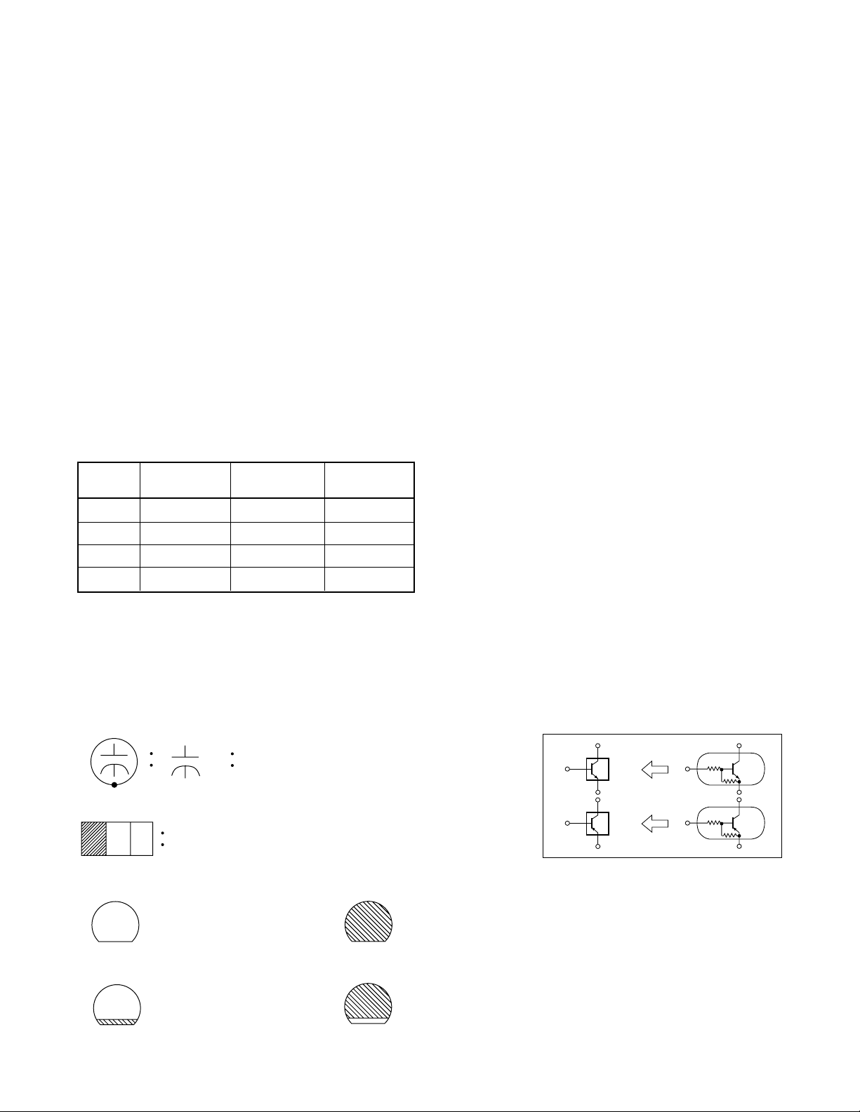
Capacitor Temperature Markings
Mark
(B)
(F)
(SR)
(Z)
Capacity
change rate
±10%
+30 - 80%
±15%
+30 - 80%
Standard
temperature
20°C
20°C
20°C
20°C
Temperatur
range
-25~+85°C
-25~+85°C
-25~+85°C
-10~+70°C
Notes:
1. Do not use the part number shown on these drawings for ordering. The correct part number is shown
in the parts list, and may be slightly different or
amended since these drawings were prepared.
2. All resistance values are indicated in ohms (K=103,
M=106).
3. Resistor wattages are 1/4W or 1/6W unless otherwise specified.
4. All capacitance values are indicated in µF
(P=10-6 µF).
5. All voltages are DC voltages unless otherwise specified.
6. Electrical parts such as capacitors, connectors, diodes, IC's, transistors, resistors, switches, and fuses
are identified by four digits. The first two digits are
not shown for each component. In each block of the
diagram, there is a note such as shown below to
indicate these abbreviated two digits.
Capacitors and transistors are represented by the
following symbols.
CBA Symbols
(Top View) (Bottom View)
+
Electrolytic Capacitor
Bottom View)
Transistor or Digital Transistor
E C B
(Top View)
E C B
(Top View)
E C B
NPN Transistor
NPN Digital Transistor
(Top View)
E C B
(Top View)
E C B
PNP Transistor
PNP Digital
Transistor
Schematic Diagram Symbols
Digital Transistor
1-3-1
SC-FN2
LIST OF CAUTION, NOTES, AND SYMBOLS USED IN THE SCHEMATIC DIAGRAMS ON THE FOLLOWING
1
".
".
3
2
1
PAGES:
1. CAUTION:
FOR CONTINUED PROTECTION AGAINST FIRE HAZARD, REPLACE ONLY WITH THE SAME TYPE FUSE.
2. CAUTION:
Fixed Voltage (or Auto voltage selectable) power supply circuit is used in this unit.
If Main Fuse (F1001) is blown, first check to see that all components in the power supply circuit are not defective
before you connect the AC plug to the AC power supply. Otherwise it may cause some components in the power
supply circuit to fail.
3. Note:
(1)Do not use the part number shown on the drawings for ordering. The correct part number is shown in the parts
list, and may be slightly different or amended since the drawings were prepared.
(2)To maintain original function and reliability of repaired units, use only original replacement parts which are listed
with their part numbers in the parts list section of the service manual.
4. Wire Connectors
(1)Prefix symbol “CN” means “connector” (can disconnect and reconnect).
(2)Prefix symbol “CL” means “wire-solder holes of the PCB” (wire is soldered directly).
5. Voltage indications for PLAY modes on the schematics are as shown below:
Unit: Volts
5.0
231
5.0
PLAY mode
Indicates that the voltage
is not consistent here.
6. How to read converged lines
-D3
Distinction Area
Line Number
(1 to 3 digits)
Examples:
1. "1-D3" means that line number "1" goes to area "D3
2. "1-B1" means that line number "1" goes to area "B1
7. Test Point Information
: Indicates a test point with a jumper wire across a hole in the PCB.
: Used to indicate a test point with a component lead on foil side.
: Used to indicate a test point with no test pin.
AREA D3
1-B1
AREA B1
1-D3
ABCD
: Used to indicate a test point with a test pin.
1-3-2
SC-FN2

DVD Main 2/3 Schematic Diagram (DV-SL10W, DV-SL10, DV-SL10X, DV-SL10(RU))
1-3-3
1-3-4 E5754SCD2
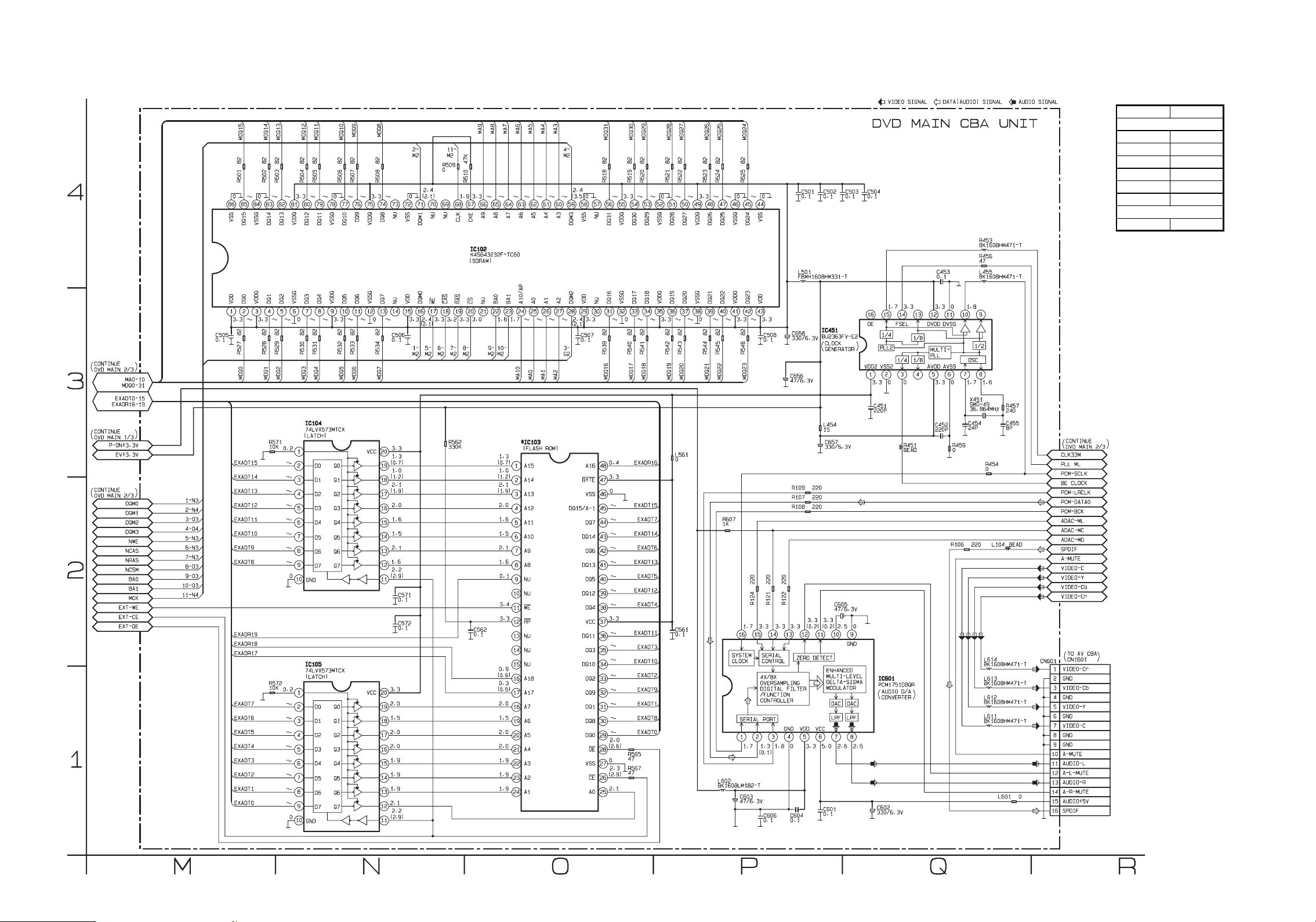
DVD Main 3/3 Schematic Diagram (DV-SL10W, DV-SL10, DV-SL10X, DV-SL10(RU))
Note:
*
IC103 is not supplied separately.
Be sure to replace with the DVD Main CBA unit when servicing IC103.
DVD MAIN 3/3
Ref No. Position
ICS
IC102 O-4
IC103 O-3
IC104 N-3
IC105 N-1
IC451 P-3
IC601 Q-1
CONNECTOR
CN601 R-1
1-3-5 1-3-6
E5754SCD3

AV 1/3 Schematic Diagram (DV-SL10W, DV-SL10, DV-SL10X, DV-SL10(RU))
CAUTION !
Fixed voltage ( or Auto voltage selectable ) power supply circuit is used in this unit.
If Main Fuse (F1001) is blown, check to see that all components in the power supply
circuit are not defective before you connect the AC plug to the AC power supply.
Otherwise it may cause some components in the power supply circuit to fail.
CAUTION
FOR CONTINUED PROTECTION AGAINST FIRE HAZARD,
REPLACE ONLY WITH THE SAME TYPE FUSE.
NOTE :
The voltage for parts in hot circuit is measured
using hot GND as a common terminal.
AV 1/3
Ref No. Posi tion
ICS
IC1001 B-1
IC1002 D-4
IC1006 C-1
TRANSISTORS
Q1001 B-3
Q1002 D-3
Q1003 B-2
Q1004 E-3
Q1005 D-2
Q1006 D-1
Q1008 A-1
Q1010 D-2
Q1011 D-1
Q1012 D-2
Q1014 E-3
Q1015 D-2
Q1016 E-2
Q1050 D-3
CONNECTOR
CN1001 F-4
1-3-7 1-3-8
E5754SCAV1

AV 2/3 Schematic Diagram (DV-SL10W, DV-SL10, DV-SL10X, DV-SL10(RU))
1-3-9
1-3-10
AV 2/3
Ref No. Posi tion
ICS
IC1201 H-1
IC1402 I-3
TRANSISTORS
Q1201 J-1
Q1202 J-1
Q1203 I -2
Q1204 I -1
Q1351 K-4
Q1352 H-2
CONNECTOR
CN1601 G-3
E5754SCAV2
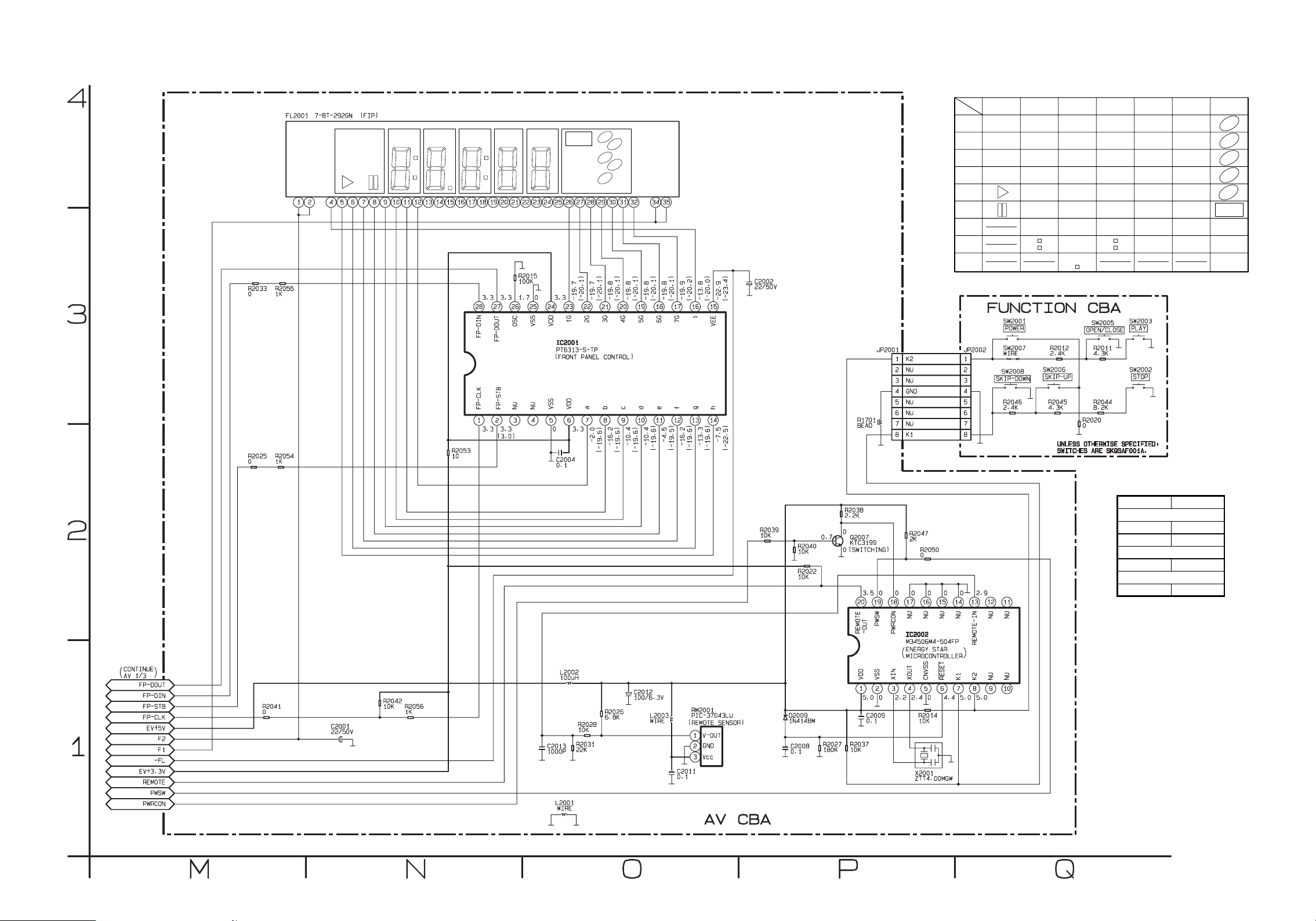
AV 3/3 & Function Schematic Diagram (DV-SL10W, DV-SL10, DV-SL10X, DV-SL10(RU))
7G 6G 5G 4G 3G 2G 1G
a
b
c
d
e
f
g
c
d
e
f
g
c
d
e
f
g
c
d
e
f
g
c
d
e
f
g
c
d
e
f
g
h
i
a
b
a
b
a
b
a
b
a
b
FL2001 MATRIX CHART
STANDBY
TITLE CHP. TRK. CD
V
PBC
DVD
REPEAT
A
-B
1
3
2
4
5
7G 5G 3G 1G4G6G 2G
STANDBY
REPEAT
A-B
TRK.CHP.TITLE
DVD
a
cb
VCD
d
PBC
ef
g
1
2
3
4
5
AV 3/3
Ref No. Position
ICS
IC2001 O-3
IC2002 P-2
TRANSISTOR
Q2007 P-2
CONNECTOR
JP2001 P-3
1-3-11 1-3-12
E5754SCAV3
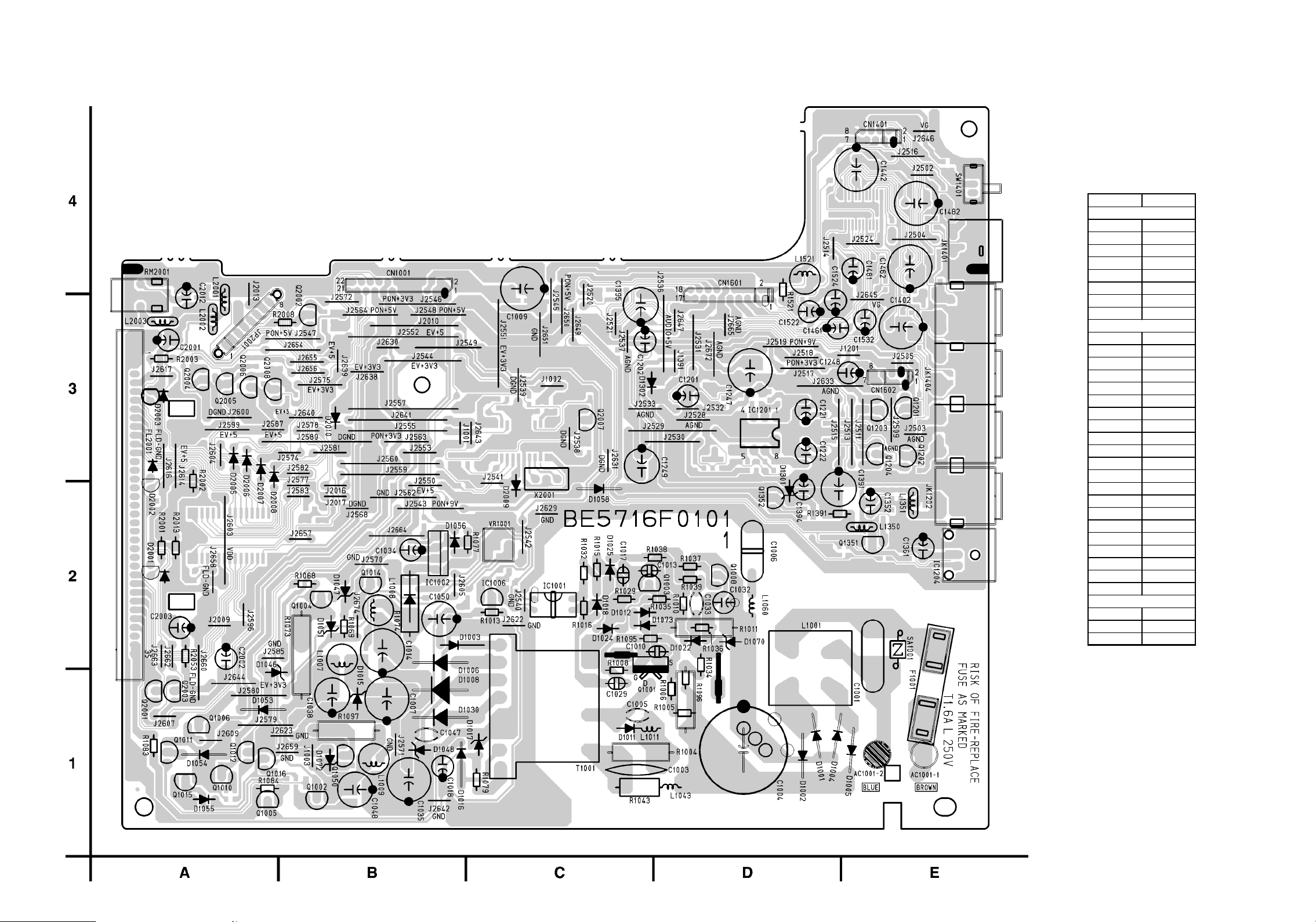
AV CBA Top View (DV-SL10W, DV-SL10, DV-SL10X, DV-SL10(RU))
CAUTION !
Fixed voltage ( or Auto voltage selectable ) power supply circuit is used in this unit.
If Main Fuse (F1001) is blown, check to see that all components in the power supply
circuit are not defective before you connect the AC plug to the AC power supply.
Otherwise it may cause some components in the power supply circuit to fail.
CAUTION
FOR CONTINUED PROTECTION AGAINST FIRE HAZARD,
REPLACE ONLY WITH THE SAME TYPE FUSE.
NOTE :
The voltage for parts in hot circuit is measured
using hot GND as a common terminal.
AV CBA
Ref No. Position
ICS
IC1001 C-2
IC1002 B-2
IC1006 C-2
IC1201 D-3
IC1204 E-2
IC1402 E-4
IC2001 A-2
IC2002 C-3
TRANSISTORS
Q1001 C-1
Q1002 B-1
Q1003 D-2
Q1004 B-2
Q1005 A-1
Q1006 A-1
Q1008 D-2
Q1010 A-1
Q1011 A-1
Q1012 A-1
Q1014 B-2
Q1015 A-1
Q1016 A-1
Q1050 B-1
Q1201 E-3
Q1202 E-3
Q1203 E-3
Q1204 E-3
Q1351 E-2
Q1352 D-2
Q2007 C-3
CONNECTORS
CN1001 B-4
CN1601 D-4
JP2001 A-4
1-3-13
1-3-14
BE5716F01011
 Loading...