

Page 1
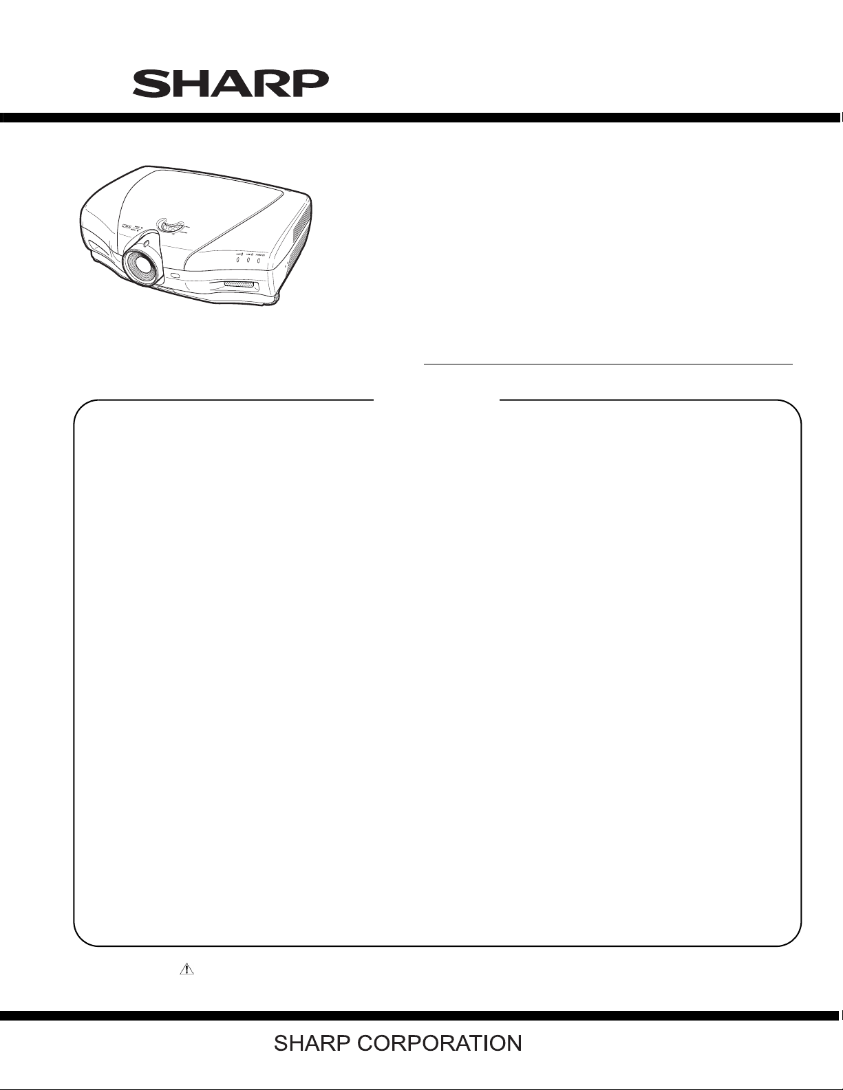
TopPage
XV-Z20000/XV-Z21000/DT-5000
SERVICE MANUAL
No. S96W3XVZ20000
DLP PROJECTOR
XV-Z20000
XV-Z21000
CONTENTS
SAFETY PRECAUTION
IMPORTANT SERVICE SAFETY NOTES.............i
Precautions for using lead-free solder ...............v
CHAPTER 1. OPERATION MANUAL
[1] Specifications ................................................. 1-1
[2] Parts Name and Basic Operation................... 1-2
[3] DIMENSIONS ................................................ 1-7
[4] Resetting the total lamp timer ........................ 1-8
CHAPTER 2. REMOVING OF MAJOR PARTS
[1] Removing the Top body ................................. 2-1
[2] Removing the Fans and PWB Unit Assem-
bly................................................................... 2-2
[3] Removing the Rear panel assembly, PC I/F
PWB and the Main PWB ................................ 2-3
[4] Precaution on Mounting the PC I/F PWB........ 2-4
[5] Removing the Power unit shield assembly
and Power/Ballast assembly .......................... 2-5
[6] Removing the Optical mechanism unit, R/C
Front PWB and IRIS Drive PWB .................... 2-6
[7] Removing the Lamp unit, CW fan, Outlet
Fan, Lamp duct, Lamp fan, Bimetal, Temp
sensor and Formatter unit. ............................. 2-7
MODELS
CHAPTER 5. TROUBLE SHOOTING TABLE
[1] TROUBLE SHOOTING TABLE ..................... 5-1
CHAPTER 6. BLOCK DIAGRAM/OVERALL WIRING
DIAGRAM
[1] BLOCK DIAGRAM.........................................6-1
[2] OVERALL WIRING DIAGRAM ......................6-3
CHAPTER 7. PRINTED WIRING BOARD
[1] MAIN Unit ......................................................7-1
[2] FORMATTER Unit .........................................7-9
[3] POWER/BALLAST Unit...............................7-17
[4] PC I/F Unit ...................................................7-23
[5] KEY Unit ......................................................7-31
[6] R/C Front Unit..............................................7-32
[7] R/C Rear Unit ..............................................7-33
[8] LED Unit ......................................................7-34
[9] IRIS DRIVE Unit .......................................... 7-35
[10] BALLAST CONTROL Unit...........................7-36
CHAPTER 8. WAVEFORMS
[1] WAVEFORMS ...............................................8-1
[2] WAVEFORM MEASUREMENT CONDI-
TION ..............................................................8-1
DT-5000
CHAPTER 3. THE OPTICAL UNIT OUTLINE
[1] THE OPTICAL UNIT OUTLINE...................... 3-1
CHAPTER 4. ELECTRICAL ADJUSTMENT
[1] ELECTRICAL ADJUSTMENT........................ 4-1
[2] Process menu ................................................ 4-4
Parts marked with " " are important for maintaining the safety of the set. Be sure to replace these parts with specified ones for maintaining the
safety and performance of the set.
CHAPTER 9. SCHEMATIC DIAGRAM
[1] DESCRIPTION OF SCHEMATIC DIA-
GRAM............................................................ 9-1
[2] SCHEMATIC DIAGRAM ................................9-2
Parts Guide
This document has been published to be used for
after sales service only.
The contents are subject to change without notice.
Page 2
XV-Z20000/XV-Z21000/DT-5000
XV-Z20000
SAFETY PRECAUTION
IMPORTANT SERVICE SAFETY NOTES
IMPORTANT SERVICE SAFETY NOTES (for USA)
Service work should be performed only by qualified service technicians who are
thoroughly familiar with all safety checks and servicing guidelines as follows:
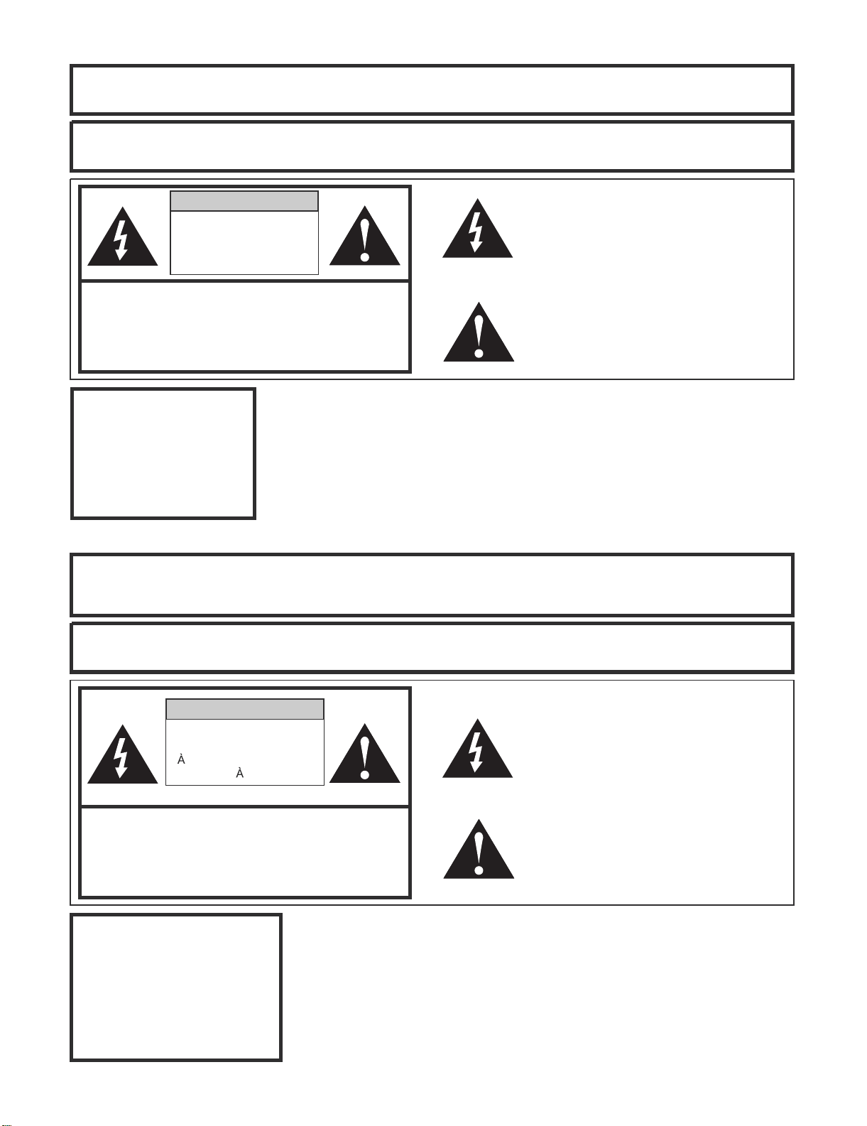
WARNING
1. For continued safety, no modification of any circuit
should be attempted.
2. Disconnect AC power before servicing.
BEFORE RETURNING THE PROJECTOR:
(Fire & Shock Hazard)
Before returning the projector to the user, perform
the following safety checks:
1. Inspect lead wires are not pinched between the chassis
and other metal parts of the projector.
2. Inspect all protective devices such as non-metallic
control knobs, insulating materials, cabinet backs,
adjustment and compartment covers or shields,
isolation resistor-capacity networks, mechanical
insulators, etc.
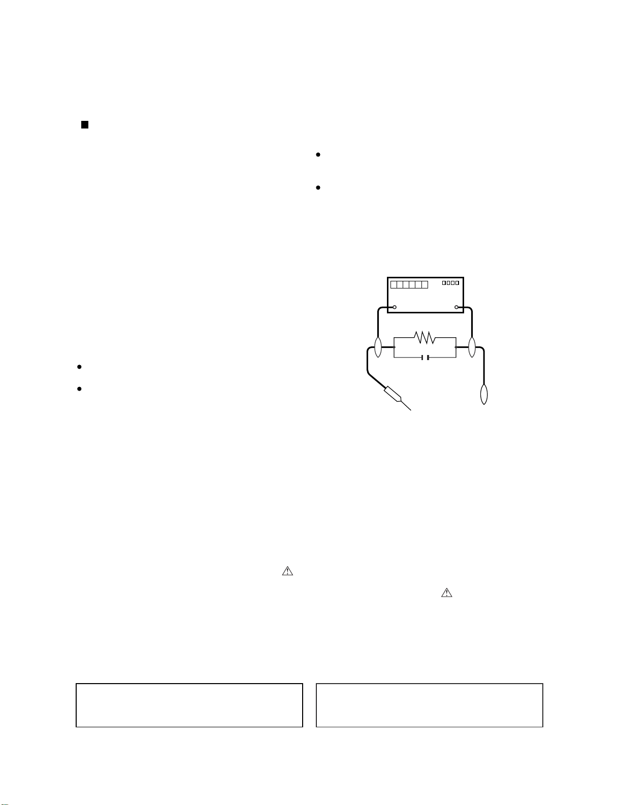
3. To be sure that no shock hazard exists, check for
current leakage in the following manner:
Plug the AC cord directly into a 120-volt AC outlet, (Do
not use an isolation transformer for this test).
Using two clip leads, connect a 1.5k ohm, 10 watt
resistor paralleled by a 0.15μF capacitor in parallel
between all exposed metal cabinet parts and earth
ground.
Service Manual
Use an AC voltmeter with sensitivity of 5000 ohm per
volt., or higher, sensitivity to measure the AC voltage
drop across the resistor.
All checks must be repeated with the AC plug
connection reversed. (If necessary, a non-polarized
adapter plug must be used only for the purpose of
completing these checks.)
Any reading of 0.3 volts RMS (this corresponds to 0.2
milliamp. AC.) or more is excessive and indicates a
potential shock hazard which must be corrected before
returning the unit to the owner.
DVM
AC SCALE
1.5k ohm
10W
0.15 μF
TEST PROBE
TO EXPOSED
METAL PARTS
CONNECT TO
KNOWN EARTH
GROUND
/////////////////////////////////////////////////////////////////////////////////////////////////////////////////////////////////////////////////
SAFETY NOTICE
Many electrical and mechanical parts in DMD™
Projector have special safety-related characteristics.
These characteristics are often not evident from visual
inspection, nor can protection afforded by them be
necessarily increased by using replacement components
rated for higher voltage, wattage, etc.
Replacement parts which have these special safety
characteristics are identified in this manual; electrical
components having such features are identified by “ ”
and shaded areas in the Replacement Parts Lists and
Schematic Diagrams. For continued protection,
replacement parts must be identical to those used in
the original circuit. The use of a substitute replacement
parts which do not have the same safety characteristics
as the factory recommended replacement parts shown
in this service manual, may create shock, fire or other
hazards.
WARNING: The bimetallic component has the primary
conductive side exposed. Be very careful in
handling this component when the power is on.
AVIS POUR LA SECURITE
De nombreuses pièces, électriques et mécaniques, dans
les projecteur à DMD™ présentent des caractéristiques
spéciales relatives à la sécurité, qui ne sont souvent pas
évidentes à vue.
Le degré de protection ne peut pas être nécessairement
augmentée en utilisant des pièces de remplacement
étalonnées pour haute tension, puissance, etc.
Les pièces de remplacement qui présentent ces
caractéristiques sont identifiées dans ce manuel;
les pièces électriques qui présentent ces particularités
sont identifiées par la marque “ ” et hachurées dans la
liste des pièces de remplacement et les diagrammes
schématiques. Pour assurer la protection, ces pièces
doivent être identiques à celles utilisées dans le circuit
d’origine. L’utilisation de pièces qui n’ont pas les mêmes
caractéristiques que les pièces recommandées par l’usine,
indiquées dans ce manuel, peut provoquer des
électrocutions, incendies ou autres accidents.
AVERTISSEMENT: La composante bimétallique dispose du
conducteur primaire dénudé. Faire attention
lors de la manipulation de cette
composante sous tension.
/////////////////////////////////////////////////////////////////////////////////////////////////////////////////////////////////////////////////
i
Page 3
XV-Z20000/XV-Z21000/DT-5000
NOTE POUR LE PERSONNEL
D’ENTRETIEN
PRECAUTION POUR LES RADIATIONS UV
La source de lumière, la lampe UHP, dans le projecteur
LCD émet de petites quantités de radiation UV.
EVITEZ TOUTE EXPOSITION DIRECTE DES
YEUX ET DE LA PEAU.
Pour votre sécurité, nous vous prions de respecter
les points suivants:
Précautions pour les radiations UV
et la lampe moyenne pression
NOTE TO SERVICE
PERSONNEL
UV-RADIATION PRECAUTION
The light source, UHP lamp, in the LCD proje ctor
emits small amounts of UV-Radiation.
AVOID DIRECT EYE AND SKIN EXPOSURE.
To ensure safety please adhere to the following:
UV-Radiatio n and Medium Pressure
Lamp Precautions
//////////////////////////////////////////////////////////////
//////////////////////////////////////////////////////////////
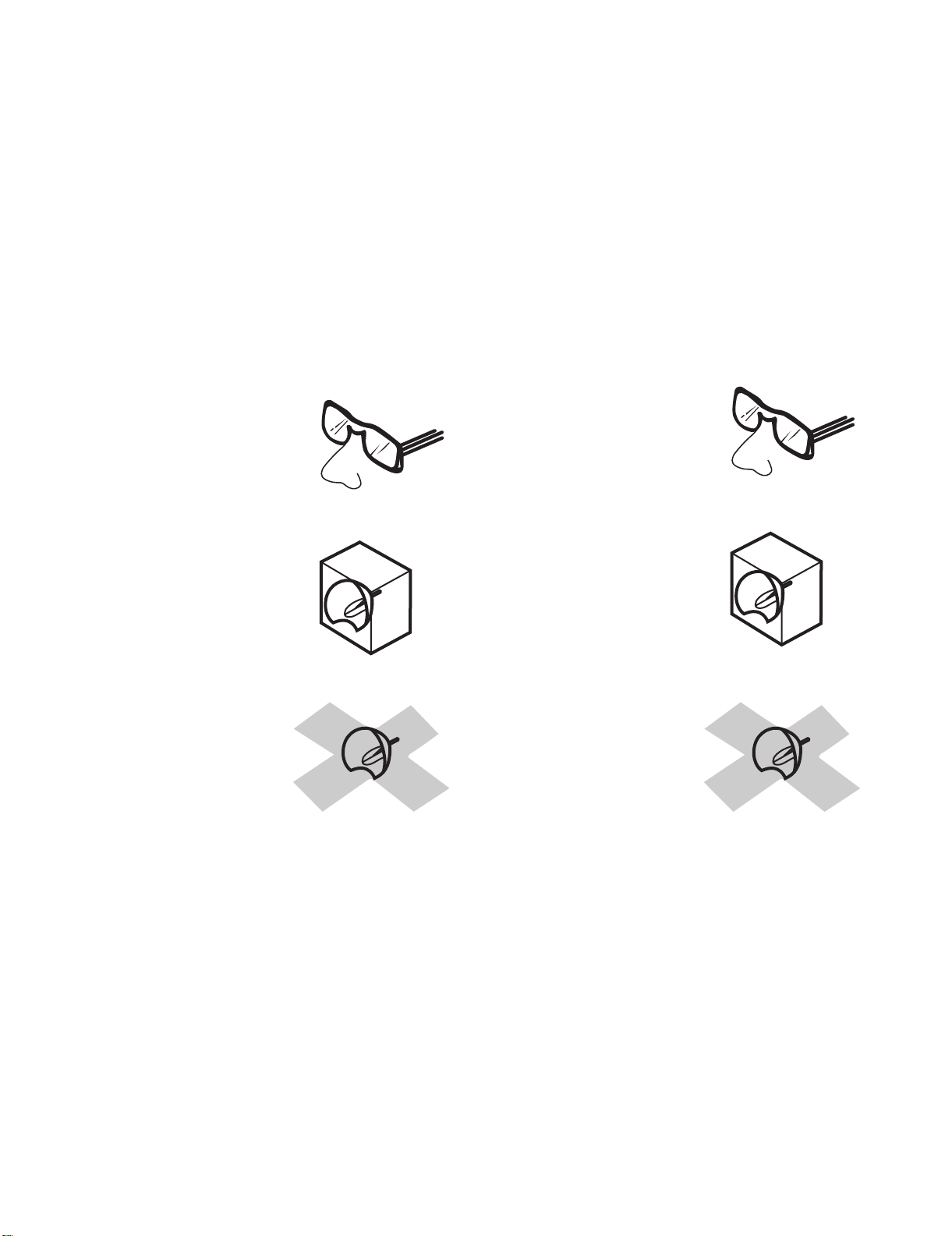
1. Be sure to wear sun-glasses when servicing the
projector with the lamp
turned “on” and the top
enclosure removed.
2. Do not operate the lamp outside of the lamp housing.
//////////////////////////////////////////////////////////////
//////////////////////////////////////////////////////////////
1. Toujours porter des lunettes de soleil lors d’un entretien
du projecteur
avec la lampe allumée
et le haut du coffret retiré.
2. Ne pas faire fonctionner la lampe à l’extérieur du boîtier
de lampe.
3. Do not operate for more than 2 hours with the enclosure
removed.
1. Be sure to disconnect the AC plug when replacing the
lamp.
2. Allow one hour for the unit to cool down before
servicing.
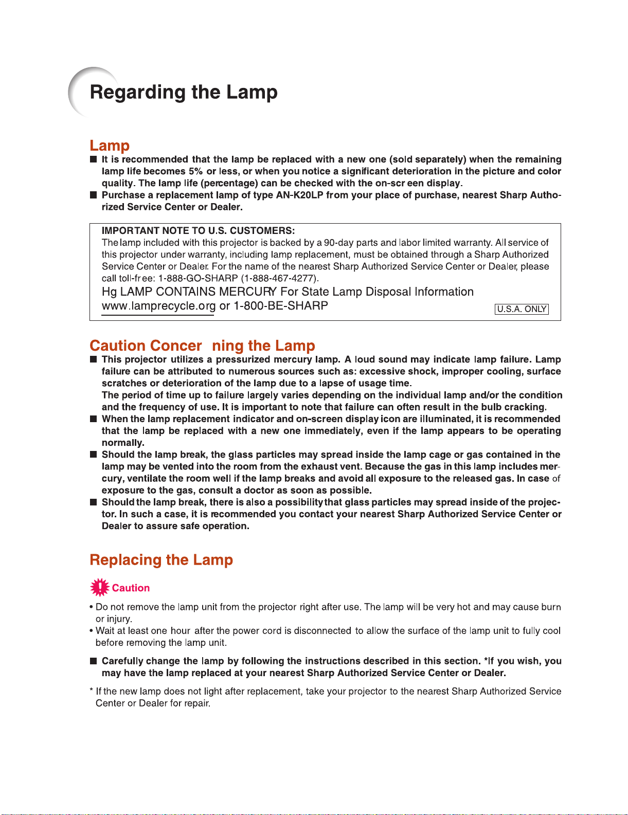
3. Replace only with same type lamp. Type AN-K20LP
rated 355V/220W.
4. The lamp emits small amounts of UV-Radiation, avoid
direct-eye contact.
5. The medium pressure lamp involves a risk of explosion.
Be sure to follow installation instructions described
below and handle the lamp with care.
3. Ne pas faire fonctionner plus de 2 heures avec le coffret
retiré.
1. Toujours débrancher la fiche AC lors du remplacement
de la lampe.
2. Laisser l’unité refroidir pendant une heure avant de
procéder à l’entretien.
3. Ne remplacer qu’avec une lampe du même type. Type
AK-K20LP, caractéristique 355/220W.
4. La lampe émet de petites quantités de radiation UVéviter tout contact direct avec les yeux.
5. La lampe moyenne pression implique un risque
d’explosion. Toujours suivre les instructions
d’installation décrites ci-dessous et manipuler la lampe
avec soin.
ii
Page 4
XV-Z20000/XV-Z21000/DT-5000
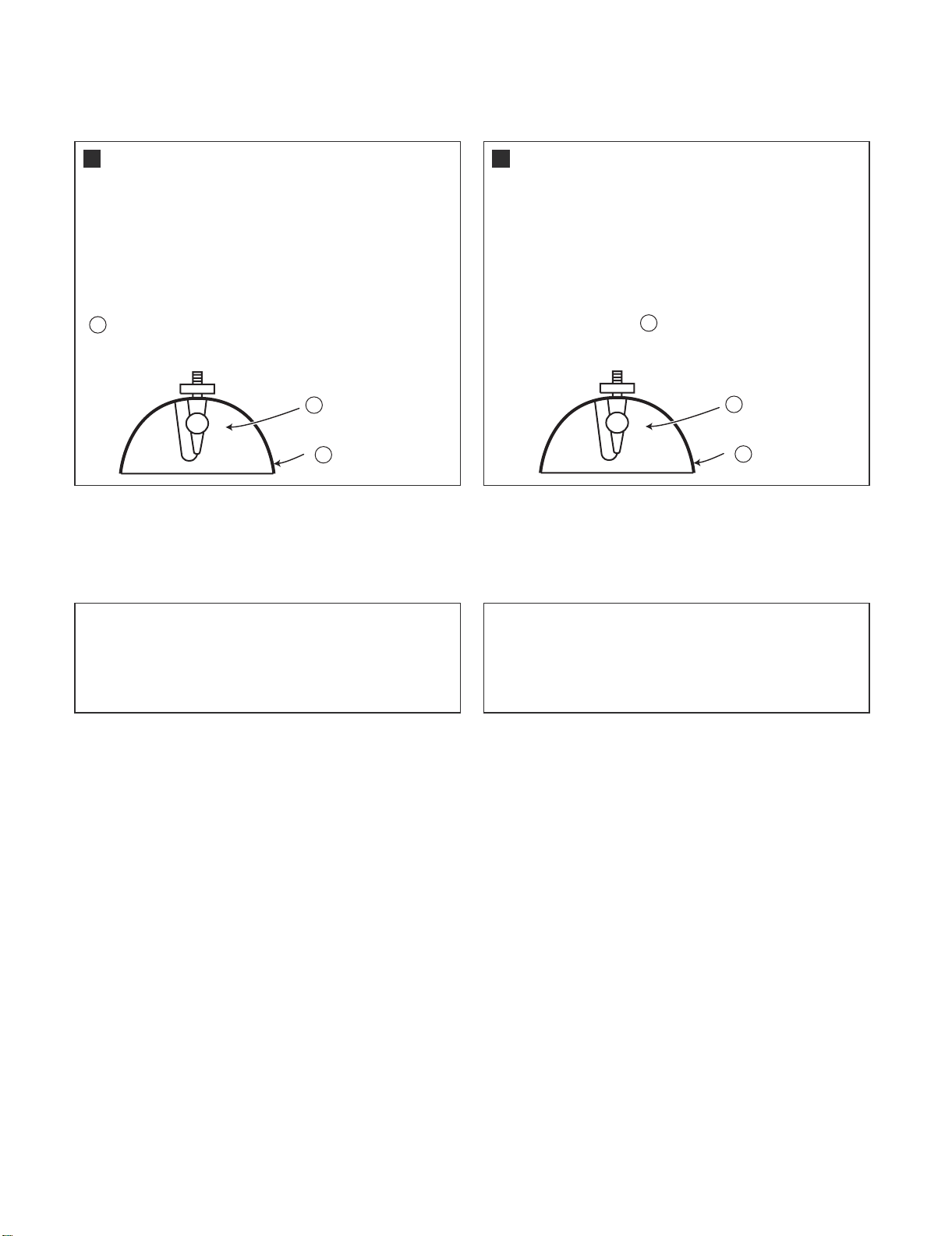
Remplacement de la lampe
Remarque:
DANGER !
UV-RADIATION PRECAUTION (Continued)
Lamp Replacement
Note:
DANGER !
PRECAUTION POUR LES RADIA
////////////////////////////////////////////////////////////////
////////////////////////////////////////////////////////////////
Since the lamp reaches a very high temperature during
units operation replacement of the lamp should be
done at least one hour after the power has been turned
off. (to allow the lamp to cool off.)
Installing the new lamp, make sure not to touch the
lamp (bulb) replace the lamp by holding its reflector
2
.
[Use original replacement only.]
Lamp
1
Reflector
2
–– Never turn the power on without the
lamp to avoid electric-shock or damage of the devices
since the stabilizer generates high voltages at its start.
////////////////////////////////////////////////////////////////
////////////////////////////////////////////////////////////////
Comme la lampe devient très chaude pendant le
fonctionnement de l’unité, son remplacement ne doit
être effectué au moins une heure après avoir coupé
l’alimentation (pour permettre à la lampe de refroidir).
En installant la nouvelle lampe, s’assurer de ne pas
toucher la lampe (ampoule). Remplacer la lampe en
tenant son réflecteur .
[N’utiliser qu’un remplacement d’origine.]
–– Ne jamais mettre sous tension sans la
lampe pour éviter un choc électrique ou des
dommages des appareils car le stabilisateur génère
de hautes tensions à sa mise en route.
2
TIONS UV (Suite)
1
Lampe
2
Reflecteur
Since small amounts of UV-radiation are emitted
from an opening between the exhaust fans, it is recommended to place the cap of the optional lens on
the opening during servicing to avoid eye and skin
exposure.
Comme de petites quantités de radiation UV sont
émises par une ouverture entre les ventilateurs aspirants, il est recommandé de placer le capuchon de
l’optique optionnelle sur l’ouverture pendant l’entretien
pour éviter une exposition des yeux et la peau.
iii
Page 5
XV-Z20000/XV-Z21000/DT-5000
WARNING: High brightness light source, do not stare into the beam of light, or view directly. Be especially
careful that
children do not stare directly in to the beam of light.
WARNING: TO REDUCE TH E RISK OF FIRE OR ELECTRIC SHOCK, DO NOT EXPOSE
THIS UNIT TO
MOISTURE OR WET LOCATIONS.
CAUTION
AVERTISSEMENT: Source lumineuse de grande intensité. Ne pas fixer le faisceau lumineux ou le regarder
directement. Ve
iller particulièrement à éviter que les enfants ne fixent directement le
faisceau lumineux.
AVERTISSEMENT: AFIN D’EV
ITER TOUT RISQUE D’INCENDIE OU D’ELECTROCUTION, NE PAS PLACER
CET APPAREIL DANS UN ENDROIT HUMIDE OU MOUILLE.
ATTENTION
CAUTION
(POWER Unit)
PRECAUTION
(Unité de PUTSSANCE)
CAUTION: TO REDUCE THE RISK OF ELECTRIC SHOCK,
NO USER-SERVICEABLE PARTS EXCEPT LAMP UNIT.
For continued
protection against a
risk of fire, replace
only with same type
6.3AH, AC250V fuse (F701)
1.6AL, AC250V fuse (F702)
REFER SERVICING TO QUALIFIED SERVICE
RISK OF ELECTRIC SHOCK.
DO NOT REMOVE SCREWS
EXCEPT SPECIFIED USER
SERVICE SCREW.
DO NOT REMOVE CABINET.
PERSONNEL.
The lighting flash with arrowhead within a
triangle is intended to tell the user that
parts inside the product are risk of electric
shock to persons.
The exclamation point within a triangle is
intended to tell the user that important
operating and servicing instructions are in
the manual with the projector.
//////////////////////////////////////////////////////////////////////////////////////////////////////////////////////////////////
RISQUE D’ÉLECTROCUTION.
NE PAS RETIRER LES VIS
RÉSERVÉE L’ENTRETIEN.
L’éclair terminé d’une flèche à l’intérieur
d’un triangle indique à l’utilisateur que les
pi‘eces se trouvant dans l’appareil sont
L’EXCEPTION DE LA VIS
susceptibles de provoquer une décharge
électrique.
Le point d’exclamation à l’intérieur d’un
D’ELECTROCUTION, NE PAS RETIRER LE CAPOT.
AUCUNE DES PIECES INTERIEURES N’EST REPARABLE
PAR L’UTILISATEUR, A L’EXCEPTION DE L’UNITE DE
LAMPE. POUR TOUTE REPARATION, S’ADRESSER A UN
Pour une protection
continue contre un
risques d’incendie, ne
remplacer qu’avec un
fusible 6.3AH, AC250V fuse (F701)
1.6AL, AC250V fuse (F702)
ATTENTION: POUR EVITER TOUT RISQUE
TECHNICIEN D’ENTRETIEN QUALIFIE.
triangle indique à l’utilisateur que les
instructions de fonctionnement et
d’entretien sont détaillées dans les
documents fournis avec le projecteur.
iv
Page 6
XV-Z20000/XV-Z21000/DT-5000
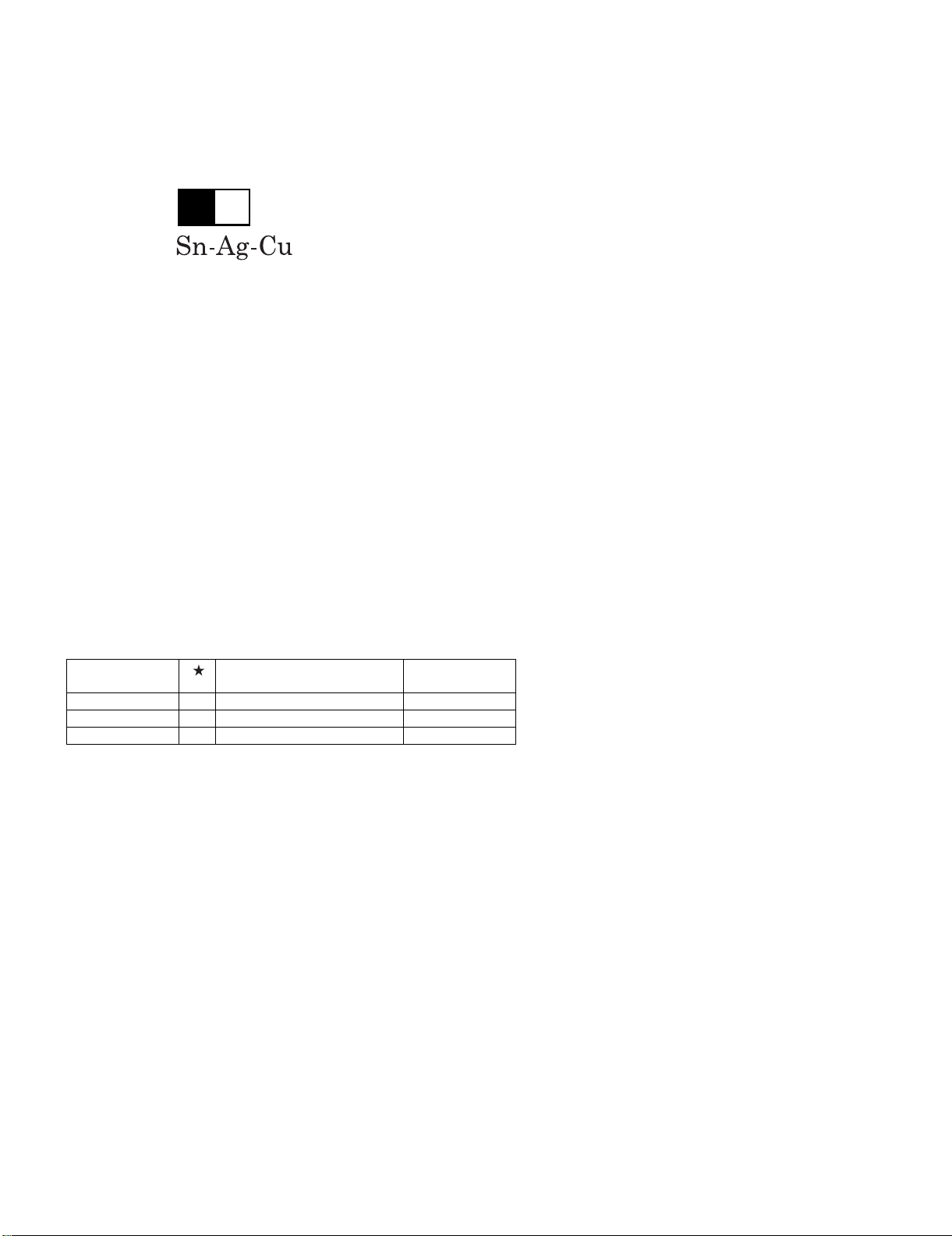
Precautions for using lead-free solder
Employing lead-free solder
• "PWBs" of this model employs lead-free solder. The LF symbol indicates lead-free solder, and is attached on the PWBs and service manuals. The
alphabetical character following LF shows the type of lead-free solder.
Example:
L Fa
Indicates lead-free solder of tin, silver and copper.
Using lead-free wire solder
• When fixing the PWB soldered with the lead-free solder, apply lead-free wire solder. Repairing with conventional lead wire solder may cause damage or accident due to cracks.
As the melting point of lead-free solder (Sn-Ag-Cu) is higher than the lead wire solder by 40 °C, we recommend you to use a dedicated soldering
bit, if you are not familiar with how to obtain lead-free wire solder or soldering bit, contact our service station or service branch in your area.
Soldering
• As the melting point of lead-free solder (Sn-Ag-Cu) is about 220 °C which is higher than the conventional lead solder by 40 °C, and as it has poor
solder wettability, you may be apt to keep the soldering bit in contact with the PWB for extended period of time. However, Since the land may be
peeled off or the maximum heat-resistance temperature of parts may be exceeded, remove the bit from the PWB as soon as you confirm the
steady soldering condition.
Lead-free solder contains more tin, and the end of the soldering bit may be easily corroded. Make sure to turn on and off the power of the bit as
required.
If a different type of solder stays on the tip of the soldering bit, it is alloyed with lead-free solder. Clean the bit after every use of it.
When the tip of the soldering bit is blackened during use, file it with steel wool or fine sandpaper.
• Be careful when replacing parts with polarity indication on the PWB silk.
Lead-free wire solder for servicing
Part No. Description Code
ZHNDAi123250E J φ0.3mm 250g(1roll) BL
ZHNDAi126500E J φ0.6mm 500g(1roll) BK
ZHNDAi12801KE J φ1.0mm 1kg(1roll) BM
v
Page 7
XV-Z20000
CHAPTER 1. OPERATION MANUAL
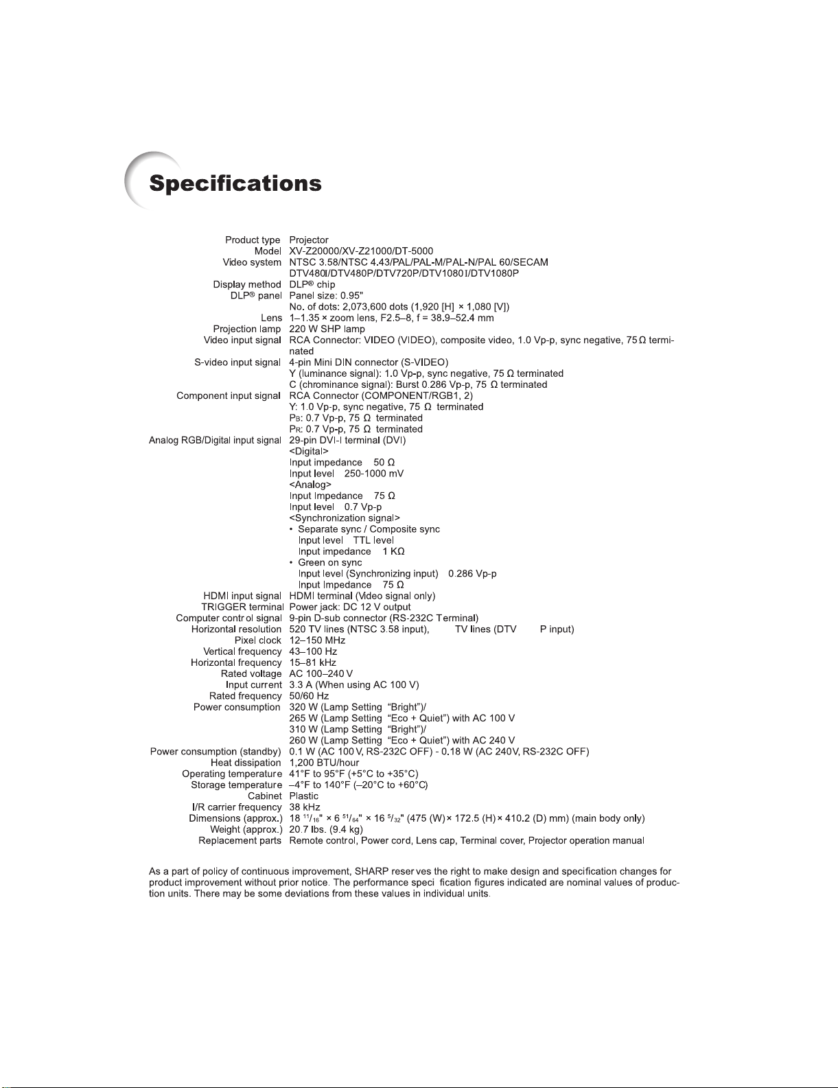
[1] Specifications
XV-Z20000/XV-Z21000/DT-5000
Service Manual
1080
1080
1 – 1
Page 8
XV-Z20000/XV-Z21000/DT-5000
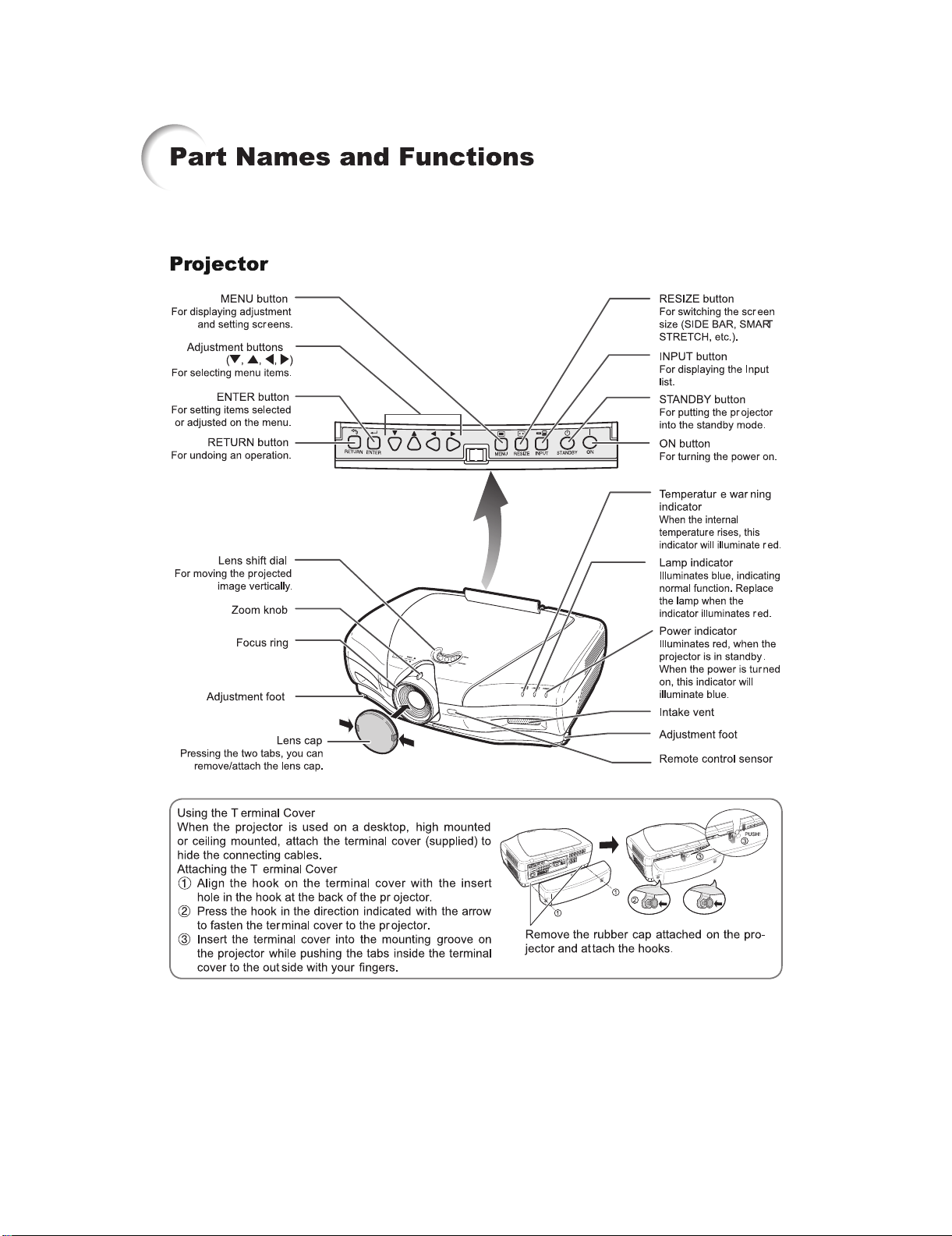
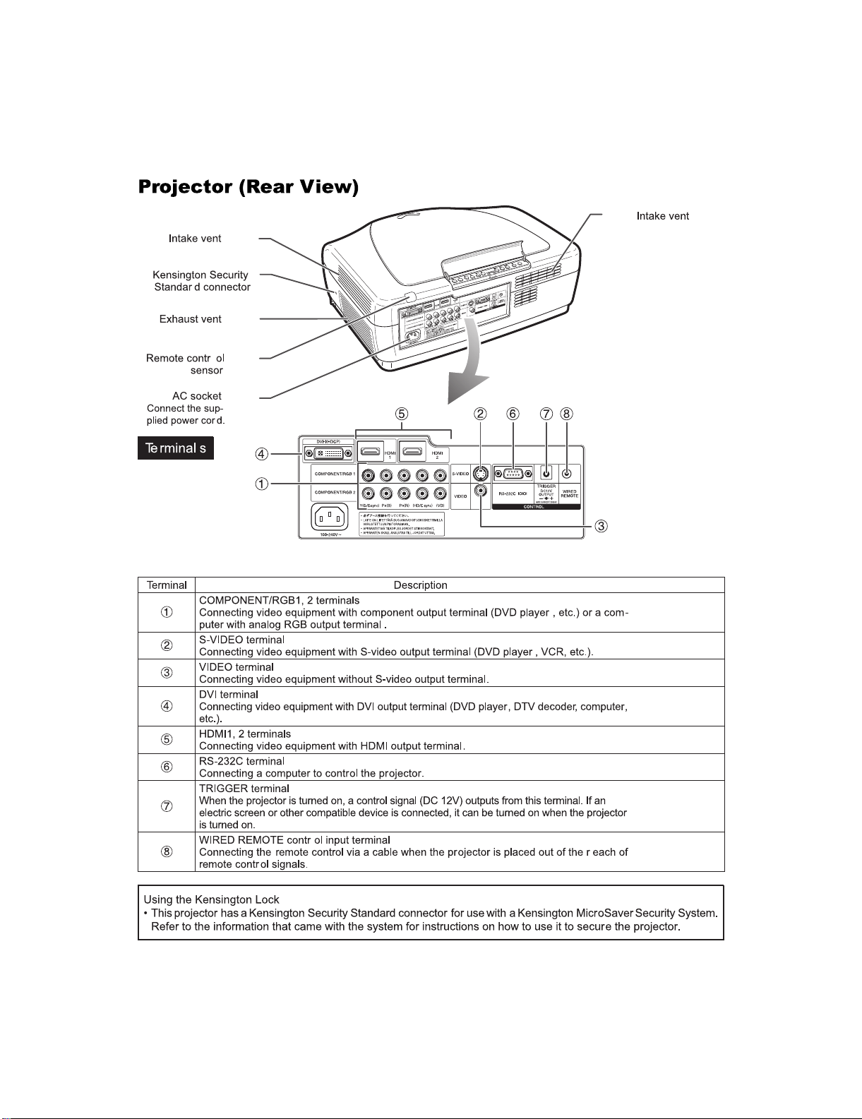
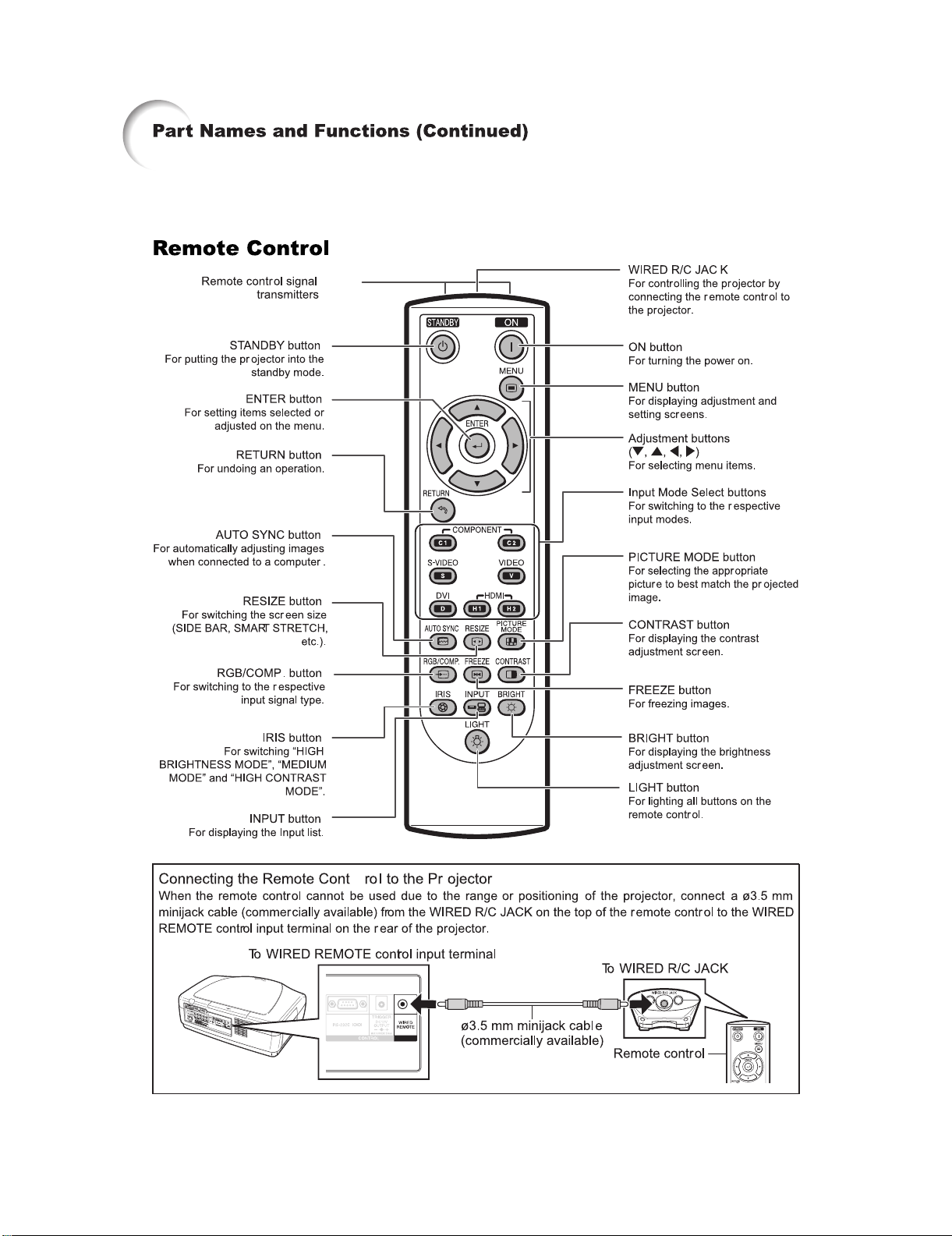
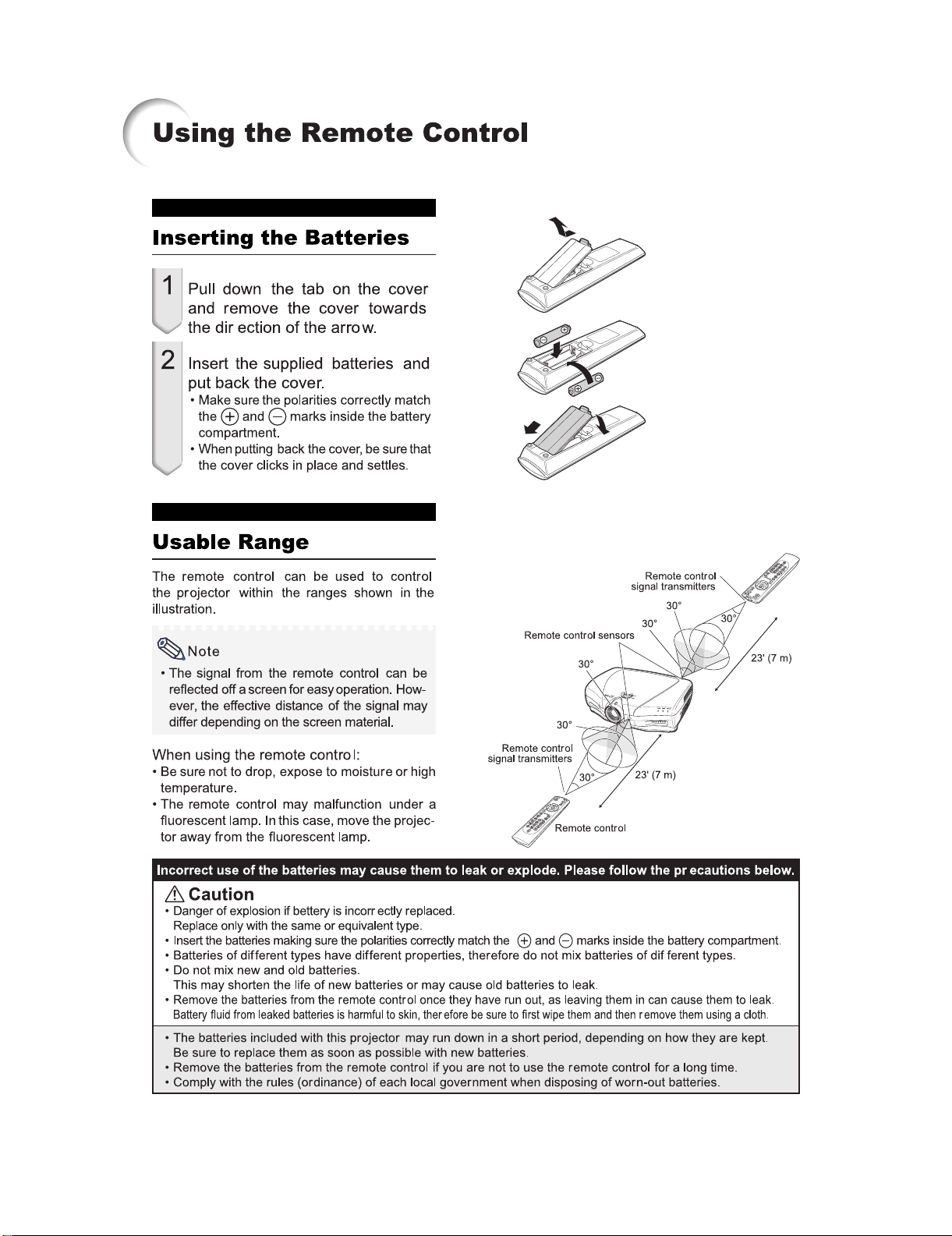
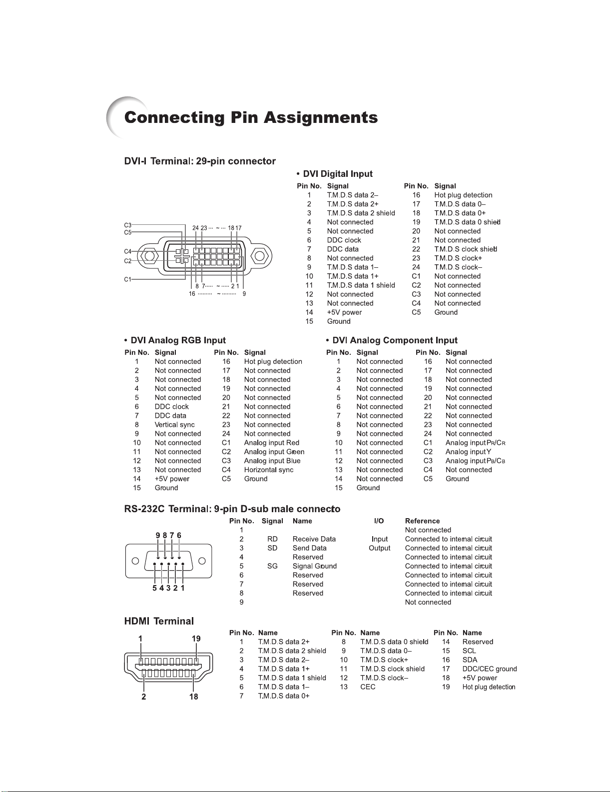
[2] Parts Name and Basic Operation
1 – 2
Page 9
XV-Z20000/XV-Z21000/DT-5000
1 – 3
Page 10
XV-Z20000/XV-Z21000/DT-5000
1 – 4
Page 11
XV-Z20000/XV-Z21000/DT-5000
1 – 5
Page 12
XV-Z20000/XV-Z21000/DT-5000
1 – 6
Page 13
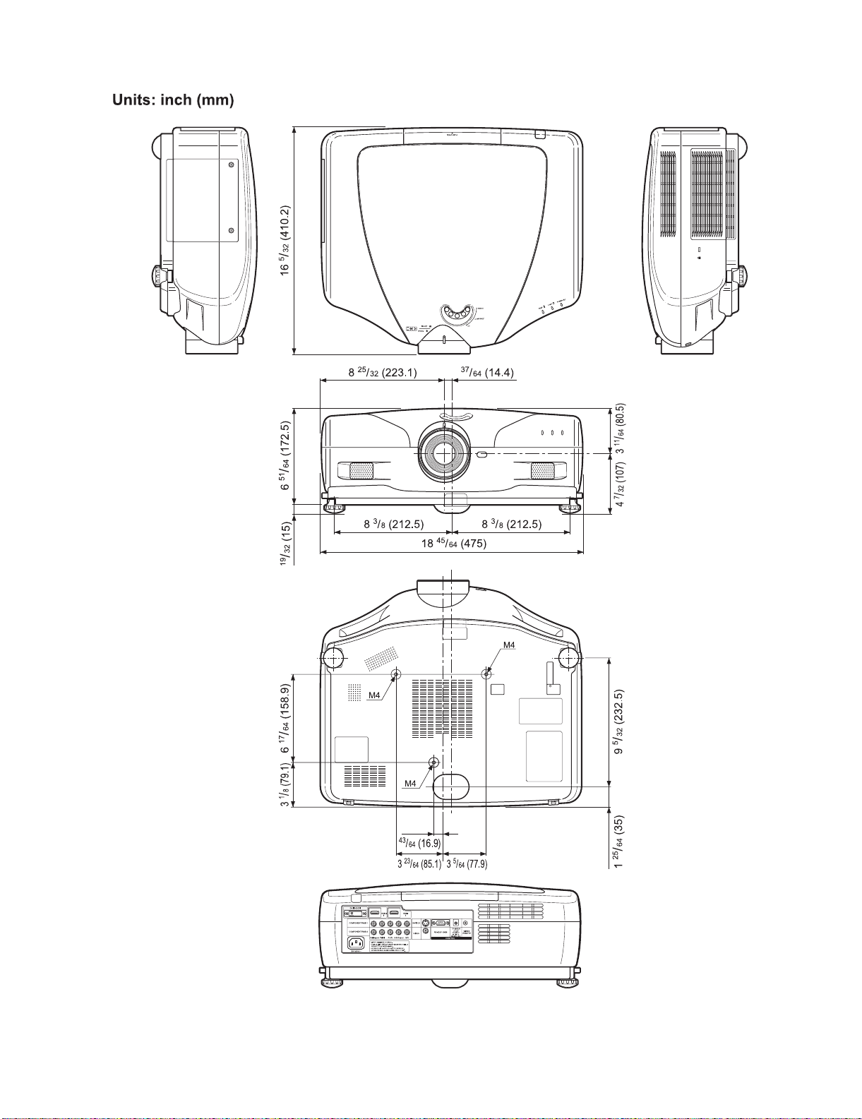
[3] DIMENSIONS
XV-Z20000/XV-Z21000/DT-5000
1 – 7
Page 14
XV-Z20000/XV-Z21000/DT-5000
[4] Resetting the total lamp timer
1 – 8
Page 15
XV-Z20000/XV-Z21000/DT-5000
1 – 9
Page 16
XV-Z20000/XV-Z21000/DT-5000
1 – 10
Page 17
XV-Z20000
CHAPTER 2. REMOVING OF MAJOR PARTS
Service Manual
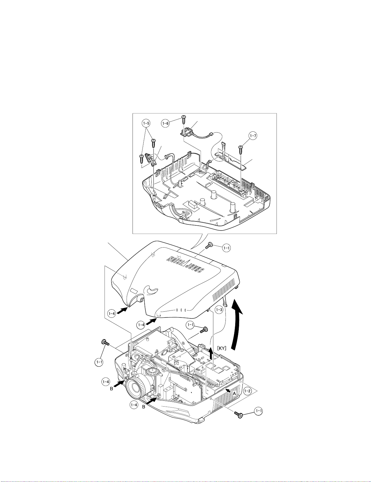
[1] Removing the Top body
1. Remove the six lock screws.
2. Press on side Arrow A of the Bottom body and lift the Rear of the Top body.
3. Dissconnect the connector.
4. Press on front Arrow B of the Bottom body and unhook the claws, and detach the Top body.
5. Remove the 2 screws and detach the LED PWB.
6. Remove the one screw and detach the R/C Rear PWB.
7. remove the three screws and detach the Operation PWB.
R/C Rear PWB
LED PWB
XV-Z20000/XV-Z21000/DT-5000
Operation
PWB
Top body
2 – 1
Page 18
XV-Z20000/XV-Z21000/DT-5000
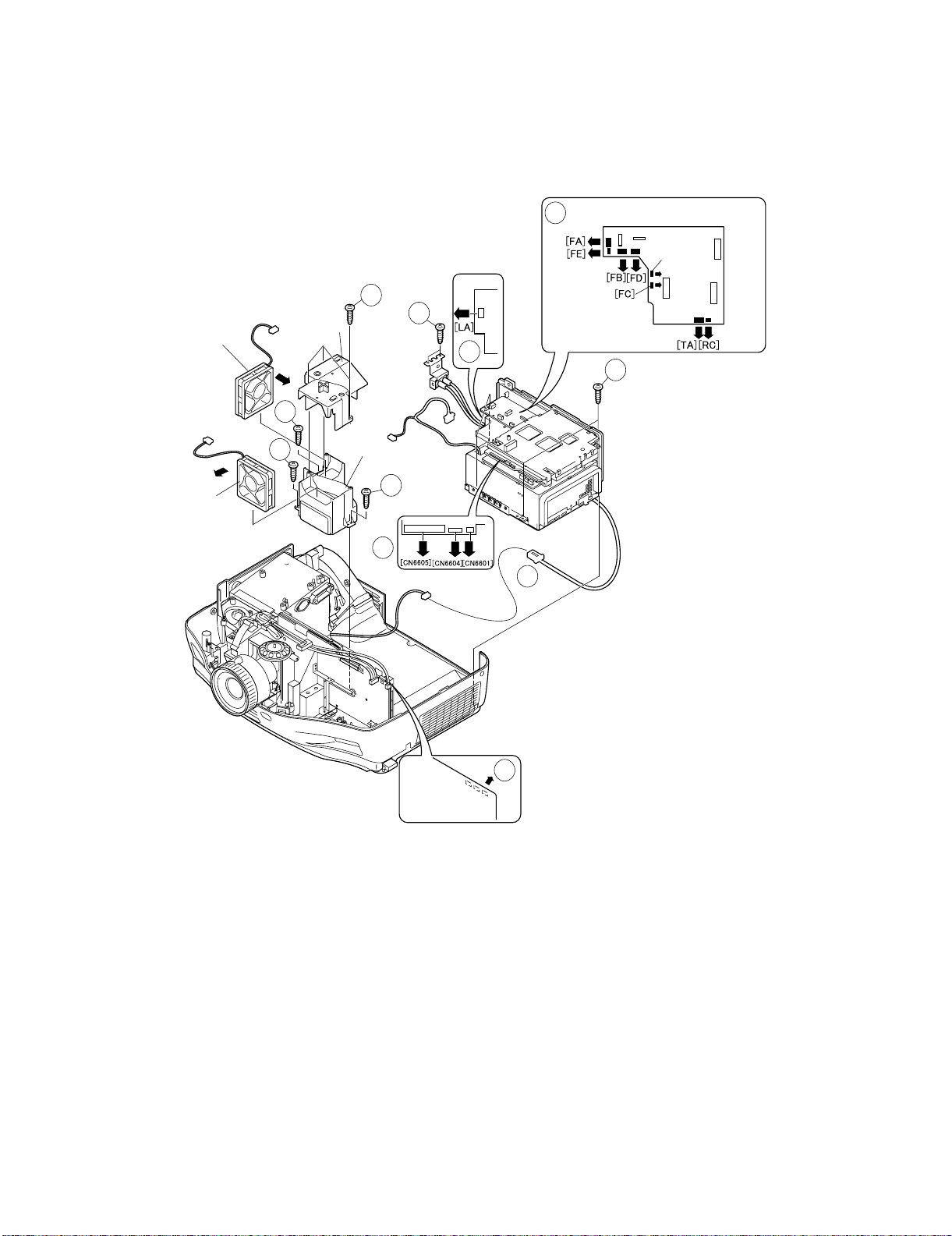
[2] Removing the Fans and PWB Unit Assembly
1. Dissconnect the fourteen connectors.
2. Remove the two screws and detach the Lamp socket.
3. Remove the three screws and detach the Intake duct (upper). Detach the two Fans.
4. Remove the four screws and detach the PWB Unit Assembly.
5. Remove the three screws and detach the Intake duct (lower).
2-1
[TB]
Fan
Fan
2-5
2-5
Intak
duct
(upper)
2-3
2-2
2-1
2-4
Intake duct
2-5
2-1
2-1
P9702
2 – 2
2-1
Page 19
XV-Z20000/XV-Z21000/DT-5000
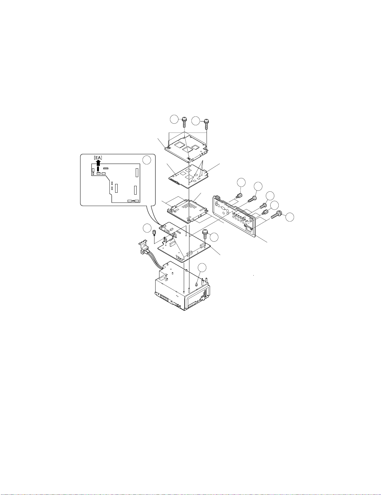
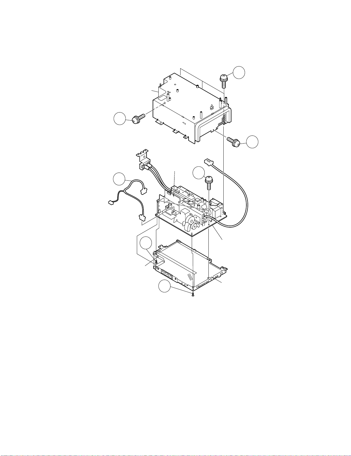
[3] Removing the Rear panel assembly, PC I/F PWB and the Main PWB
1. Remove the three screw.
2. Remove the two screws.
3. Remove the two screws.
4. Remove the four hexagonal supports and detach the Rear panel assembly.
5. Remove the four screws and detach the PC I/F assembly.
6. Remove the two screws and remove the four socket, and detach the shields.
7. Remove the one connector.
8. Remove the three screws and remove the two hexagonal supports.
9. Remove the one hook and detach the Main PWB.
Upper shield
3-7
Socket
hook
3-8
3-5
3-6
Socket
lower shield
3-9
PC I/F PWB
hook
3-8
Main PWB
3-4
3-1
Rear panel assembly
3-2
3-4
3-3
2 – 3
Page 20
XV-Z20000/XV-Z21000/DT-5000
[4] Precaution on Mounting the PC I/F PWB
1. Insert the lower shield into the power supply unit.
2. Align the PC I/F PWB with the socket on the main PWB, and securely connect them by pressing the 3 socket sections from above.
3. Fit the upper shield to the lower shield.
NOTE: (1) You must pay attention to the fitting direction of the upper and lower shields (both sides). (Figures 1 and 2)
(2) The upper shield on the terminal side must not be placed on the PWB. (Figure 3)
4. Install the 2 screws (3-6).
5. Install the 4 screws (3-5).
The upper shield must be located the outer side.
Upper shield
Hook
Lower shield
The lower shield must be located
the outer side.
Hook
Lower shield
Hook
PC I/F PWB
Upper shield
Upper Shield
Figure 1
The upper shield must be located the outer side.
Hook
The lower shield must be located the outer side.
Figure 2
The upper shield must not be
placed on the PWB.
Figure 3
2 – 4
Page 21
XV-Z20000/XV-Z21000/DT-5000
B
[5] Removing the Power unit shield assembly and Power/Ballast assembly
1. Remove the five screws and remove the two hooks, and detach the Power unit shield assembly.
2. Remove the one connector.
3. Remove the two screws and remove the two hooks, and detach the Power/Ballast assembly.
NOTE: Order the Power/Ballast assembly when replacing the ballast unit.
4-1
Power unit shield.
4-1
4-1
Ballast CTR
PWB
4-3
4-2
hook
4-3
4-3
Power PW
hook
2 – 5
Page 22
XV-Z20000/XV-Z21000/DT-5000
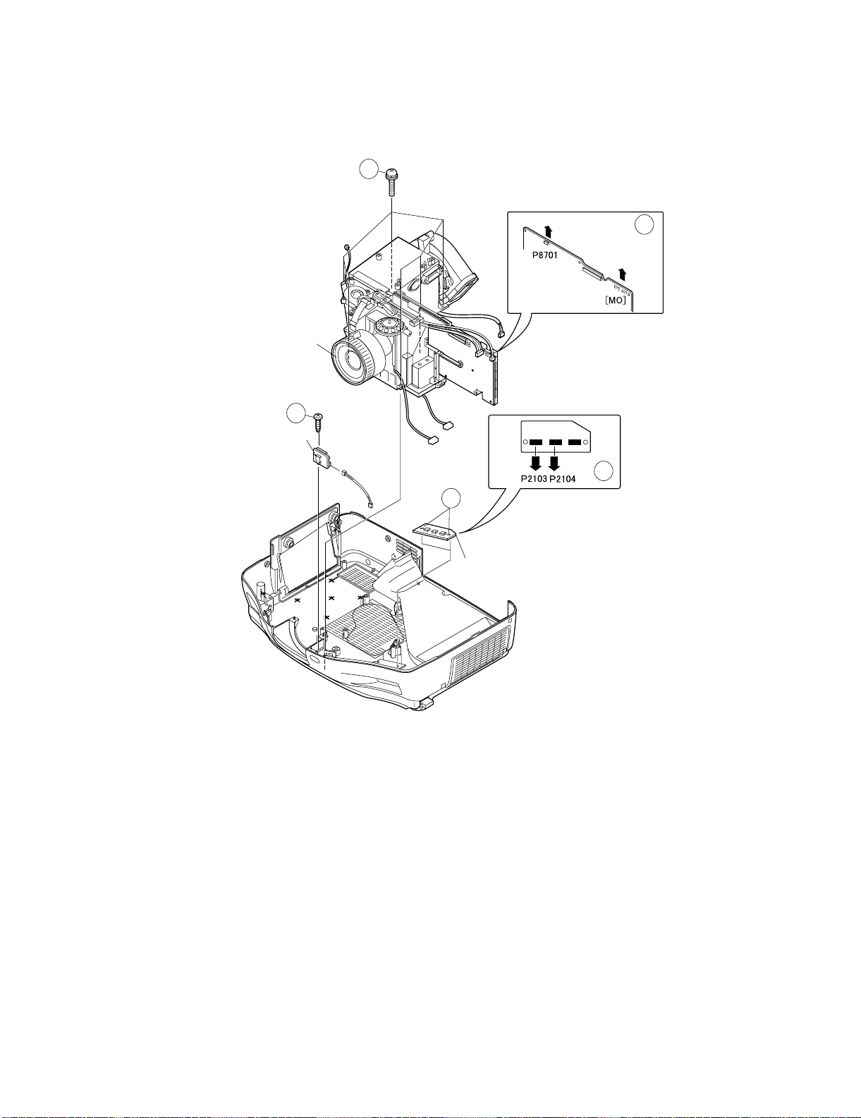
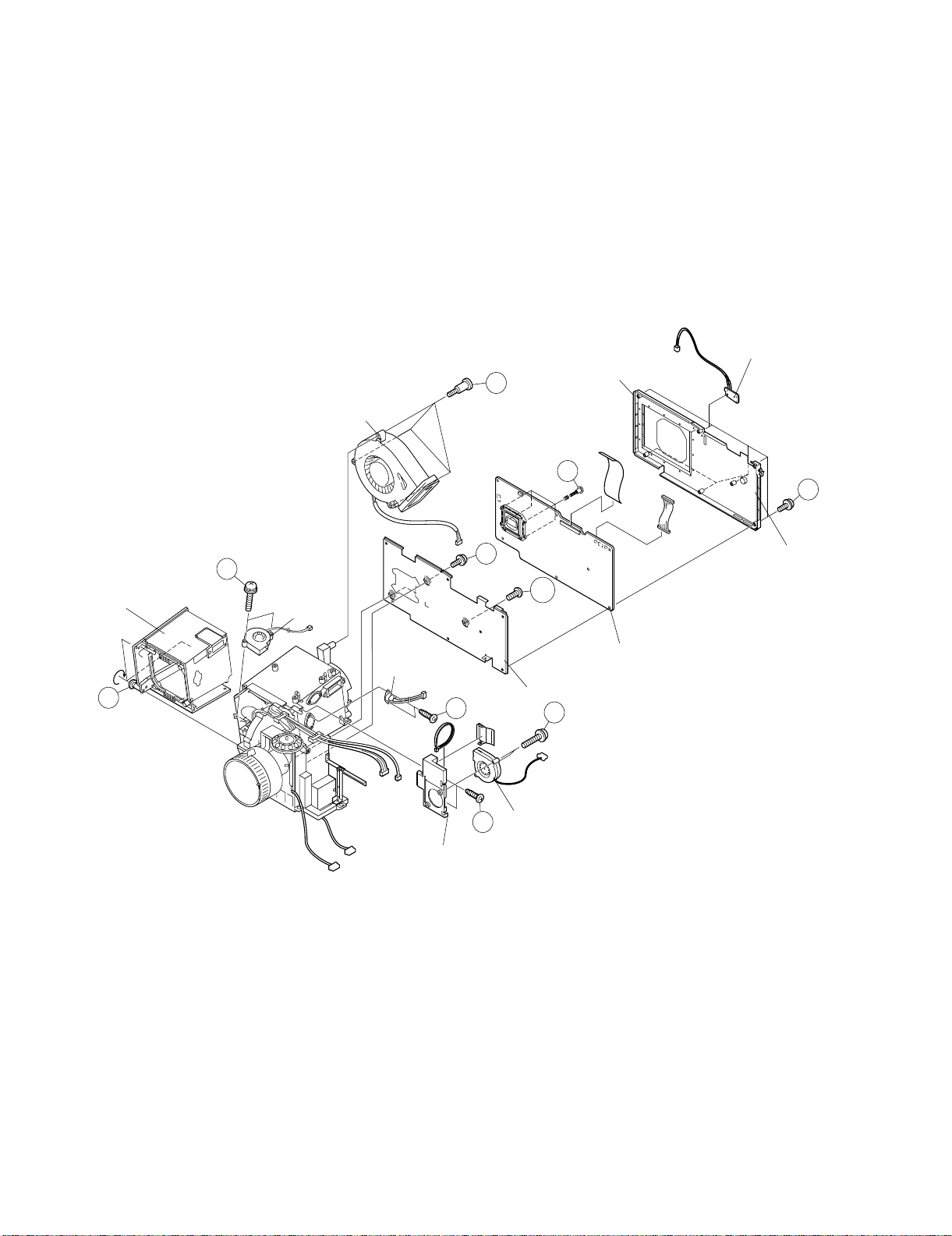
[6] Removing the Optical mechanism unit, R/C Front PWB and IRIS Drive PWB
1. Remove the four connectors.
2. Remove the six screws and detach the Optical mechanism unit.
3. Remove the one screw and the one connector. Detach the R/C Front PWB.
4. Remove the two hooks and detach the IRIS Drtive PWB.
5-2
5-1
Optical mechanism unit
5-3
R/C Front PWB
5-1
5-4
IRIS Drive PWB
2 – 6
Page 23
XV-Z20000/XV-Z21000/DT-5000
[7] Removing the Lamp unit, CW fan, Outlet Fan, Lamp duct, Lamp fan, Bimetal, Temp sensor and Formatter unit.
1. Remove the three screws and detach the Lamp unit.
2. Remove the two screws and detach the CW fan.
3. Remove the three screws and detach the Outlet fan.
4. Remove the two screws and detach the Lamp duct.
5. Remove the two screws and detach the Lamp fan.
6. Remove the two screws and detach the Bimetal.
7. Remove the seven screws and detach the Temp sensor and Formatter shield (Back).
8. Remove the four screws and detach the Formatter PWB.
9. Remove the two screws.
10.Remove the one screw and detach the Formatter shield (Front)
Lamp unit
6-1
6-2
Outlet fan
CW fan
Bimetal
6-6
6-9
6-4
6-3
Formatter shield (Front)
6-8
6-10
Formatter shield (Front)
6-5
Lamp fan
Temp sensor
6-7
Formatter
shield (Back)
Formatter PWB
Lamp duct
2 – 7
Page 24
XV-Z20000/XV-Z21000/DT-5000
XV-Z20000
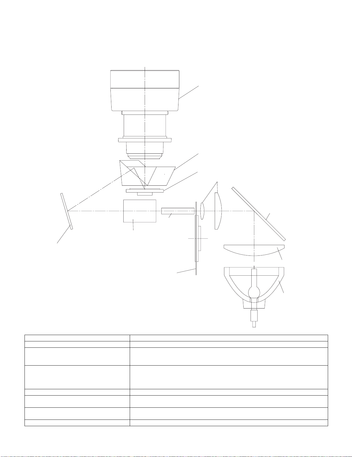
CHAPTER 3. THE OPTICAL UNIT OUTLINE
Service Manual
[1] THE OPTICAL UNIT OUTLINE
1. Layout for proper setup of the optical components and parts (top view)
Projection lens
Prism
DMD Chips
Condensor lens
IR-cut mirror
Light tunnel
Relay lens
Fold mirror
Condensor lens
Color filter
Lamp
Item Descriptions
1. Lamp The DC Light source lamp with parabola reflector.
2. Condensor lens, IR-cut mirror and light- tunnel The condensor lens leads the light generated from the lamp to the end surface of the light-tunnel through the IR-cut mirror.
The IR-cut mirror is set in this unit to eliminate the excessive heat by the lamp energy.
3. Color filter This color filter separates the white light into the 3 colors R,G and B.
A photo-sensor should be set in this unit to detect the transition timing properly between color
filters.
The maximum rotating speed is 9000rpm.
4. Relay lens and fold mirror This unit leads the illumination spot to effective area on DMD.
5. Prism This prism also leads the illumination spot to effective area on DMD and at the same time leads
the reflection lights on the DMD to the projection lens.
6. DMD chip This chip turns on and off in projection to each color component per dot depending on the input
source.
7. Projection lens This lens enlarges and projects the incidend light coming from the DMD.
3 – 1
Page 25
XV-Z20000/XV-Z21000/DT-5000
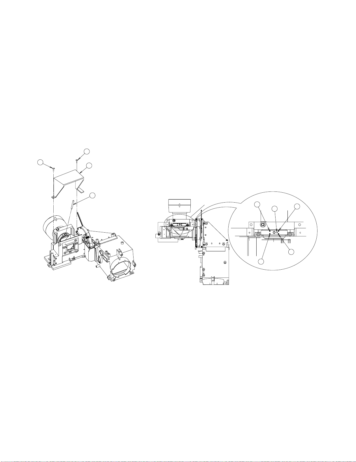
2. Adjusting the mirrors
Make adjustment by the indication territory on the screen to prevent the circumference of the screen from getting dark because a lighting range deviated.
1. Remove the top body so that the optical unit may be seen. Display white only screen on the screen.
2. Detach the mirror adjustment part cover on the bottom right of the projection lens.
3. Turn three screws with special hexagon wrench (9HPH10XL120) and adjust so that a part of the screen may not get dark because a lighting range
deviated
4. Mount the adjustment part cover .
5. Mount the top panel.
1
1
Insert hexagon wrench
in this direction.
Expansion figure of part A
3. Adjusting the back focal distance after replacing the projection lens
NOTE: A piece of temporary tape is attached on the focus ring that comes with the replacement projection lens. Keep this tape in place until the finish
of the adjustment.
1. Provide a distance of 2.4 m between the set and the screen and adjust the zoom knob to “wide end”.
2. Adjust the lens shift until the projection lens comes to the same level as the center of the screen.
3. Detach the optical unit top cover A from behind the projection lens.
4. Loosen the four hex screws B in the back of the projection lens.
5. Insert the adjustment screwdriver C (9EVDRIVERZ9000) in the hole D at the back of the lens. Put the center of the screen in the best focus. (Preferably feed the signal for 1-dot white crosshatch pattern or 1-dot white dot pattern on black background.)
6. Tighten the four hex screws B to the torque of 0.3 Nm (3.06 kgfcm), and apply screw loctite to them.
7. Peel the temporary tape off the focus ring of the projection lens.
8. Attach the optical unit top cover A back into position. Finally fix the two screws E and apply screw loctite to them.
3 – 2
Page 26
XV-Z20000/XV-Z21000/DT-5000
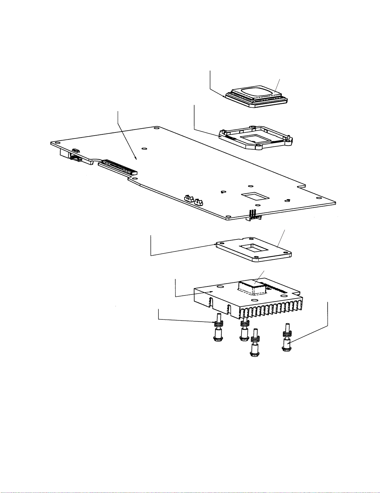
4. Joint of DMD and the unit
Wipe to clean the contamination of the PWB contacting part (gold plating part) with ethanol.
Set the position of the interposer with DMD attached to the optical unit, and then put the unit PWB on the interposer.
Sandwich the unit PWB and the back plate with the heatsink from the reverse side of the unit PWB and tighten with screws and springs.
The tightening toruqus is 0.45±0.05 Nm (4.5Kgfcm)
DMD
DMD Shield
Formatter unit
Backer plate
Interposer
Backer Plate Sheet
Carbon Sheet
Heat sink
Spring (4pcs)
Screw (4pcs)
3 – 3
Page 27
XV-Z20000/XV-Z21000/DT-5000
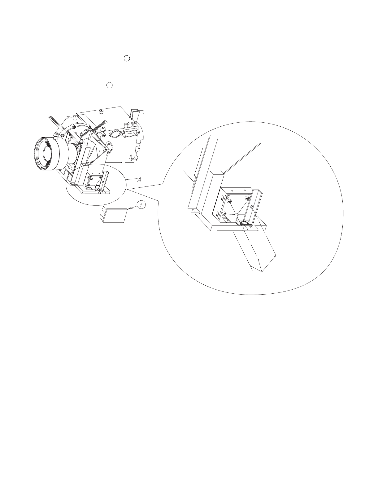
5. When the DMD unit has been replaced
NOTE: DMD chip and Formatter PWB are supplied at the same time, and an exchange only with DMD isn't done.Refer to "REMOVING OF MAJOR
PARTS" when exchanging Formatter PWB.
There is no need to readjust the back focal distance of the projection lens. If focusing is noticeably poor, however, make this readjustment.
1. Provide a distance of 2.4 m between the set and the screen.
2. Adjust the lens shift until the projection lens comes to the same level as the center of the screen.
3. Detach the optical unit top cover A from behind the projection lens.
4. Loosen the four hex screws B in the back of the projection lens.
5. Adjust the zoom knob at the front of the projection lens to "tele end" and ensure good focusing.
6. Then adjust the zoom knob at the front of the projection lens to "wide end".
7. Insert the adjustment screwdriver C (9EVDRIVERZ9000) in the hole D at the back of the lens. Put the center of the screen in the best focus. (Preferably feed the signal for 1-dot white crosshatch pattern or 1-dot white dot pattern on black background.)
8. Move the zoom knob from "wide end" back to "tele end" and see if focusing is ensured. If not, repeat the above steps (5), (6) and (7) until the best
focus is achieved.
9. Tighten the four hex screws B to the torque of 0.3 Nm (3.06 kgfcm), and apply screw loctite to them.
10.Attach the optical unit top cover A back into position. Finally fix the two screws E and apply screw loctite to them.
E
E
A
C
X
B
D
B
B
B
Expansion figure
of part X
3 – 4
Page 28
XV-Z20000/XV-Z21000/DT-5000
R
W
G
B
XV-Z20000
CHAPTER 4. ELECTRICAL ADJUSTMENT
Service Manual
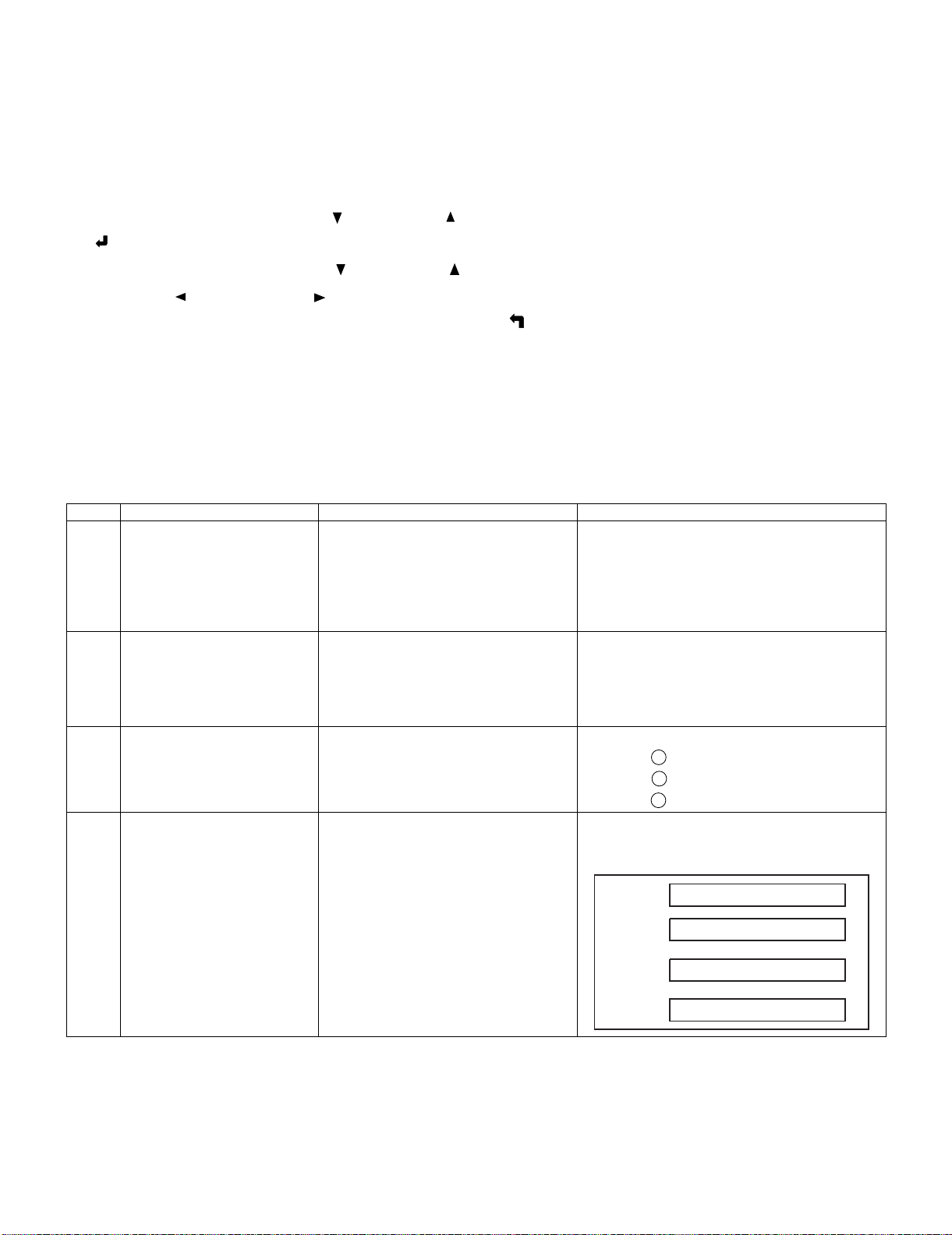
[1] ELECTRICAL ADJUSTMENT
The unit has been adjusted optimally at the time of factory shipment. However, if the screen position is deviated or when exchanging parts, make an
adjustment as shown below.
• Turn on the power (lamp on state) and wait for 15 minutes for aging.
• Enter the adjustment process mode with SW2002 (tact switch) on the main unit.
• Select the group to adjust with the DOWN ( ) key or the UP ( ) key on the remote control, and enter the adjustment item with the ENTER
( ) key on the remote control.
• Select the adjustment item with the DOWN ( ) key or the UP ( ) key on the remote control.
• Use the LEFT ( ) key or the RIGHT ( ) key for adjustment.
• To return from the adjustment item to the adjustment group, use the UNDO ( ) key.
• To exit the adjustment process mode, execute the factory setting at the end of the adjustment.
If the factory setting is not executed, the adjusted contents are not reflected.
<Cautions for adjustment>
1. Initialization and factory setting
If the initialization S1 or the factory setting S5 of EEPROM is carried out, time for writing the data is necessary.
When executing EEPROM initialization S1 or S5, the OSD of adjustment process mode disappears, and the OSD of SET1 or SET5 appears. After
completing setting, the input is switched automatically (SET1: DVI A-RGB input, SET5: C1). Never turn off the power until the input is switched (a
little less than 1 minute).
No. Adjusting point Adjusting conditions Adjusting procedure
1 EEPROM initialization 1. Turn on the power (with the lamp on) and
warm up the set for 15 minutes.
2 MODEL setting and model name
check
3 Color wheel sequence setting Check the number marked at CW.
4 Color wheel index adjustment 1. Adjustment device: DDP3021
Process menu: LINE
Select MODEL.
Adjustment group: DLP
Adjustment item: SEQUENCE
Initial value: 2
2. Adjustment group: DLP
3. Adjustment item: CWINDEX
Initial value: 40
The built-in pattern for INDEX adjustment is
displayed.
1. Make the following settings.
Press SW2002 to enter the process mode, and execute S1 to initialize EEPROM.
After executing S1, the input switches to DVIAnalogRGB.
S1: Main and Sub EEPROM initialization
S2: Sub EEPROM initialization
MODEL 0 DT5000
1 XVZ20000
2 XVZ21000
After setting, check that the model name displayed in
the first line of process menu is the same as the setting.
Color wheel number: SEQUENCE number
1
2
3
1. Adjust the setting so that the R, G and B Ramp tone
pattern should be smooth without noises.
1
2
3
4 – 1
Page 29

XV-Z20000/XV-Z21000/DT-5000
No. Adjusting point Adjusting conditions Adjusting procedure
5-1 R-bright/contrast adjustment 1. Device: AD998417
5-2 G-bright/contrast adjustment 1. Device: AD998417
5-3 B-bright/contrast adjustment 1. Device: AD998417
6-1 Component R-offset 1. Adjustment device: AD998417
6-2 Component B-offset
(Auto adjustment)
6-3 Component G-bright 1. Adjustment device: AD998417
2. Adjustment group: AD (RGB)
(Process gamma linkage)
3. Adjustment item: R-Bright
Initial value: 40
Adjustment item: R-D
Initial value: 60
4. Input terminal: DVI A-RGB (Input switching linkage)
5. Input signal: XGA
Wind pattern having 100% (0.7 Vpp) R signal and 0%
2. Adjustment group: AD (RGB)
(Process gamma linkage)
3. Adjustment item: G-Bright
Initial value: 40
Adjustment item: G-D
Initial value: 60
4. Input terminal: DVI A-RGB (Input switching linkage)
5. Input signal: XGA
Wind pattern having 100% (0.7 Vpp) G signal and 0%
2. Adjustment group: AD (RGB)
(Process gamma linkage)
3. Adjustment item: B-Bright
Initial value: 40
Adjustment item: B-D
Initial value: 60
4. Input terminal: DVI A-RGB (Input switching linkage)
5. Input signal: XGA
Wind pattern having 100% (0.7 Vpp) B signal and 0%
2. Adjustment group: AD (COMP)
(Process gamma linkage)
3. Adjustment item: CR-OFFSET
Initial value: 50
4. Input terminal: DVI A-Component
(Input switching linkage)
5. Input signal: Component 100% Ramp signal
1. Adjustment device: AD998417
2. Adjustment group: AD (COMP)
(Process gamma linkage)
3. Adjustment item: CB-OFFSET
Initial value: 50
4. Input terminal: DVI A-Component
(Input switching linkage)
5. Input signal: Component 100% Ramp signal
2. Adjustment group: AD (COMP)
(Process gamma linkage)
3. Adjustment item: G-BRIGHT
Initial value: 70
4. Input terminal: DVI A-Component
(Input switching linkage)
5. Component wind pattern having 100%
(0.7 Vpp) G signal and 0%
6. Perform adjustment after adjusting CROFFSET and CB-OFFSET.
1. Observe the 0% portion.
2. Vary R-Bright (increment direction), and adjust to
the point reduced by 1 point from the point where red
bit dropout appears.
3. Observe the 100% portion.
4. Vary R-D (increment direction), and adjust to the
point raised by 2 points from the point where red bit
dropout appears.
1. Observe the 0% portion.
2. Vary G-Bright (increment direction), and adjust to
the point reduced by 1 point from the point where
green bit dropout appears.
3. Observe the 100% portion.
4. Vary G-D (increment direction), and adjust to the
point raised by 2 points from the point where green bit
dropout appears.
1. Observe the 0% portion.
2. Vary B-Bright (increment direction), and adjust to
the point reduced by 1 point from the point where blue
bit dropout appears.
3. Observe the 100% portion.
4. Vary B-D (increment direction), and adjust to the
point raised by 2 points from the point where blue bit
dropout appears.
1. Vary CR-OFFSET, and place the red line appearing
near the center over the green line.
2. The line color turns yellow.
1. Vary CB-OFFSET, and place the blue line over the
line turning yellow by CR-OFFSET adjustment.
2. The line color turns white.
1. Observe the 0% portion.
2. Vary G-BRIGHT (decrement direction), and the
screen starts to whiten.
3. Adjust to the point where no bit dropout is found
and the screen becomes completely white.
4 – 2
Page 30

XV-Z20000/XV-Z21000/DT-5000
No. Adjusting point Adjusting conditions Adjusting procedure
6-4 Component RGB-gain adjust-
ment
(Auto adjustment)
7 White balance adjustment 1. Adjustment device: DDP3021
8 Factory setting 1. Group: SSS 1. Perform the following settings.
Do not change the process adjustment values other than the above since they are set so that optimal images are obtained.
1. Adjustment device: AD998417
2. Adjustment group: AD (COMP) (Process
gamma linkage)
3. Adjustment item: G-D
Initial value: 70
4. Input terminal: DVI A-Component
(Input switching linkage)
5. Component wind pattern having 100%
(0.7 Vpp) G signal and 0%
6. Perform adjustment after adjusting CROFFSET, CB-OFFSET and G-BRIGHT.
2. Adjustment group: DLP
3. Adjustment item: R-GAIN
Initial value: 95
B-GAIN
Initial value: 95
4. Input terminal: DVI A-Component
(Input switching linkage)
5. Input signal: Component 75% gray signal
1. Observe the 100% portion.
2. Vary G-GAIN (decrement direction), and the illuminance and chromaticity start to change.
3. Adjust to the point raised by 2 points from the point
where bit dropout appears on the screen.
1. Observe the chromaticity of 75% portion using
CL200.
2. Adjust the y value to adjustment chromaticity ±
0.005 with B-GAIN.
3. Adjust the x value to adjustment chromaticity ±
0.005 with R-GAIN.
Adjustment chromaticity
x = 0.299 ±0.005
y = 0.316 ±0.005
Destination Process adjustment Remote control
setting
Europe: S3 Factory setting 3
North America: S4 Factory setting 4
Japan: S5 Factory setting 5
China: S6 Factory setting 6
South America: S7 Factory setting 7
4 – 3
Page 31

[2] Process menu
Group Subject
AD(RGB)
AD(COMP)
DLP
VIDEO1
VIDEO2
OUTPUT
LINE
XV-Z20000/XV-Z21000/DT-5000
R-BRIGHT Adjustment Value Subject
G-BRIGHT Adjustment Value Subject
B-BRIGHT Adjustment Value Subject
R-D Adjustment Value Subject
G-D Adjustment Value Subject
B-D Adjustment Value Subject
AD-AUTO — No Use
G-BRIGHT Adjustment Value Subject
CR-OFFSET Adjustment Value Subject
CB-OFFSET Adjustment Value Subject
G-D Adjustment Value Subject
COMP-AUTO 0 Fixed Value
CW-INDEX Adjustment Value Subject
DLP-GAMMA 1 Fixed Value
R-BRIGHT 100 Fixed Value
G-BRIGHT 100 Fixed Value
B-BRIGHT 100 Fixed Value
R-GAIN Adjustment Value Subject
G-GAIN 95 Fixed Value
B-GAIN Adjustment Value Subject
CCA 0 Fixed Value
SEQUENCE Adjustment Value Subject
PICTURESUB 128 Fixed Value
PICTURE 136 Fixed Value
BRIGHT 128 Fixed Value
TINT 128 Fixed Value
N-COLOR 128 Fixed Value
P-COLOR 120 Fixed Value
SV-COLOF 5 Fixed Value
YGC-CNT 0 Fixed Value
SETUP 1 Fixed Value
CTI 7 Fixed Value
N358DLY 7 Fixed Value
PALDLY 7 Fixed Value
H-CENTER 128 Fixed Value
VIDEO-AUTO 0 Fixed Value
YTRAP FILNP 0 Fixed Value
CTRAP FILNP 0 Fixed Value
YTRAP FILS 1 Fixed Value
CTRAP FILS 2 Fixed Value
YCTRAP FIL 1 Fixed Value
YCTRAP GAIN 0 Fixed Value
FCTRAP SYS 1 Fixed Value
PEAK GAIN 128 Fixed Value
PEAK FIL 2 Fixed Value
PEAK CORING 0 Fixed Value
CR LPF 1 Fixed Value
CB LPF 1 Fixed Value
R1-GAIN 128 Fixed Value
G1-GAIN 128 Fixed Value
B1-GAIN 128 Fixed Value
V-R1-GAIN 128 Fixed Value
V-G1-GAIN 128 Fixed Value
V-B1-GAIN 128 Fixed Value
C-R1-GAIN 128 Fixed Value
C-G1-GAIN 128 Fixed Value
C-B1-GAIN 128 Fixed Value
MODEL Setting Value Setting Item
TIME — Fixed Value
LAMP 0 Fixed Value
OFF 0 Fixed Value
TEMP OFF 4 Fixed Value
SENSOR CHECK — Fixed Value
4 – 4
Page 32

XV-Z20000/XV-Z21000/DT-5000
Group Subject
S1 (Main+Sub EEPROM Initialized) —
S2 (Sub EEPROM Initialized) —
S3 (EU) —
SSS
PATT ERN
CVIC
SPECIAL
S4 (US) —
S5 (JPN) —
S6 (CHINA) —
S7 (South America) —
RGB 100% White Signal
RGB50 50% Gray Scale Signal
CROSS Crosshatch Signal
STEP Gray Step Signal
COLOR Colour Bar Signal
RAMP Lamp Signal
INDEX PATTERN Index Adjustment Signal
ENHANCED SD — Fixed Value
ENHANCED HD — Fixed Value
DNR — Fixed Value
MNR SD — Fixed Value
MNR HD — Fixed Value
UNVEIL — Fixed Value
ACC — Fixed Value
OSD DIMMER — Fixed Value
CMS HUE — Fixed Value
CMS SAT — Fixed Value
CM S VAL — F ixed Va l ue
GAMMA POS — Fixed Value
IPL
E2PROM —
ADR RD/WR —
PRG VER.
SUB VER —
FMT VER. —
—
—
—
—
4 – 5
Page 33

XV-Z20000
CHAPTER 5. TROUBLE SHOOTING TABLE
Service Manual
[1] TROUBLE SHOOTING TABLE
Checking the basic performance
XV-Z20000/XV-Z21000/DT-5000
Is the POWER LED on or flickering in red or
blue?
YES
Is the set turned on by the set's or remote
controller's power key?
YES
Is the cooling fan running? Is the lamp on? NO Go to "Checking the lamp light-up".
YES
Is the user menu displayed? NO Check the formatter circuit's peripheral circuits
YES
Is the video input (VIDEO, S-VIDEO) as
specified?
YES
Is the component input (C1, C2) as specified?
NO Go to "Checking the power unit"
NO Go to "Checking the microcomputer peripher-
als"
and go to “checking the PC PWB”
NO Are there output signals at TL3053, TL3504,
TL3517?
YES
go to “checking the PC PWB”
NO Are there output signals at TL3506, TL3508,
TL3512?
NO Check the Q2501,
Q2502, Q2504 and their
peripheral circuits.
NO Check the IC2501,
IC2502 and their peripheral circuits.
YES
Check the PC board circuit's peripheral circuits.
YES
Is the RGB input (DVI) as specified? NO Check the PC board circuit's peripheral circuits.
YES
Does the RS-232C interface function? NO Are there output signals at every other pin from
pins (10) to (40) of P3580?
YES
Check the IC5003 on the PC PWB
YES
Recommended
communication software: "TERA TERM"
Make the following settings: baud rate at
9600 bps, bit length at 8 bits, stop bit at 1 bit
and no parity. Press the RETURN key on the
keyboard. Does "ERR" show up again?
YES
END
NO Check the IC5003 on the PC PWB
NO Check the IC2001 circuit
and its peripheral circuits.
5 – 1
Page 34

XV-Z20000/XV-Z21000/DT-5000
Checking the power unit
Are all the connectors inside the
power unit tightly connected?
YES
Is the lamp cover closed completely? NO Tighten up the lamp door closed with the
YES
Is the bimetal switch off? NO Replace the bimetal switch or press the
YES
Is AC voltage applied across the
RY701 relay?
YES
Is AC voltage applied across L706? NO Replace F702.
YES
Is there DC voltage of about 6 V
across C723?
NO Insert the connectors P702, P704, CN90
and P703 tightly.
screws.
red button to reset.
NO Replace F701.
NO Check the T701, L705, R706, R718.
Replace any of them as required.
YES
Is a voltage of DC370V applied to
C737 and C740?
YES
Is there the specified voltage at the
output terminal of P704?
YES
Check the output PWB
NO Check the circuits leading to the primary
side of T704 for damage.
Replace any of them as required.
NO Check the circuits leading to the second-
ary side of T704 for damage.
Replace any of them as required.
5 – 2
Page 35

Check of the microprocessor's
peripheral circuits
XV-Z20000/XV-Z21000/DT-5000
The power indicator does not light
up?
NO
When connecting to an AC outlet, the
power indicator lights red for a
moment and flashes red at 1-second
intervals?
NO
The power indicator flashes red at 4-
second intervals?
YES
Check the voltage of TL6503 on the
PC board unit.
Is it 3V or more?
YES
Is clock output to TL5015 on the PC
board unit?
YES Check the power supply BU6V system
and output voltage of IC2810 and IC2002.
Check peripheral circuits of IC2005.
YES Check the lamp door and lamp switch. Try
to press the red button of bimetal SW.
Check each output of power supply.
NO Go to “Check of lamp lighting”.
NO Check the output voltage of DCDC regula-
tor IC on the main unit and PC board unit.
NO Are X5001 (16.59 MHz) and X5002
(32.768 MHz) oscillated?
Or check peripheral circuits of IC5003.
YES
Is pulse output to TL5009 when connecting to an AC outlet?
YES
Check peripheral circuits of IC5003,
IC5101 and IC5104.
Check of lamp lighting
The lamp indicator lights blue and goes out in
about 15 seconds. The power indicator flashes
red at 1-second intervals.
NO
The lamp flashes blue, but it lights solid red after
about one minute.
NO
The lamp lights up. After about 100 seconds, the
TEMP warning indicator appears on the screen,
and the unit enters the stand-by. (The power indicator and temperature monitor indicator flash red.)
NO Check peripheral circuits of IC2005.
YES Check the 13 V power supply and the
cooling fan drive circuit.
YES The lamp or the ballast unit is defective.
YES If TEMP error occurs even at low ambient
temperatures, check the TEMP1 and
TEMP3 signal lines. Check the fan.
NO
Go to "The lamp is flashing blue continuously".
5 – 3
Page 36

XV-Z20000/XV-Z21000/DT-5000
The lamp is flashing blue continuously.
Is a voltage of 2.5 V or more present
at pins TL6610 in the PC PWB unit?
YES
Is a voltage of 3 V or more present at
TL6611 in the PC PWB unit?
NO
Are a 1 Vp-p clock signals present at
R8731, R8732 in the formatter unit?
YES
Is power output of IC9701 and
IC9702 normal? (1.8V/1.2V/2.5V/
3.3V)
YES
Is a pulse present at each address
pin of IC8602 and IC9602 in the formatter unit, immediately after turning
the power on?
YES
Is a pulse being output to each data
pin of IC8602 and IC9602 in the for-
matter unit, immediately after turning
the power on?
NO Check IC2005 (sub-microcomputer) and
peripheral parts.
YES Check IC2005 (sub-microcomputer) and
peripheral parts.
NO Check X8701, Check the peripheral cir-
cuits of IC8711 and IC8712.
NO Check peripheral circuits of IC9701 and
IC9702.
NO IC9101 is defective.
NO IC8602 or IC9602 is defective.
YES
Are IC8602 and IC9702 warm when
touching them?
YES
Is a motor drive pulse present at pins
(2), (3), and (4) of P9701 in the formatter unit?
YES
Is a pulse present at pin (4) of P8901
in the formatter unit?
YES
IC8301 or IC9301 is defective.
NO Check IC8301 and IC9301 and peripheral
circuits of IC8601 and IC9601.
NO Check IC9701 and its peripheral circuits.
NO The color wheel unit is defective.
5 – 4
Page 37

Check the PC PWB unit.
XV-Z20000/XV-Z21000/DT-5000
Can the menu display be
brought up?
NO
Check OSD. Check the input at the compo-
YES Check the RGB input. Check the basic flow of the signals.
nents.
Check the VIDEO input. Since the VIDEO input enters CVIC through a different
Check the 480iRGB (or component) input.
Since the component and VIDEO signals follow the
same path to the output as the formatter unit uses,
after CVIC (IC6001), the check that would otherwise
be performed after the CVIC does not need to be performed. (480i and 576i are excluded.)
The signal passes through the same circuit as the
RGB input. Mainly, check the SOG (Sync On Green)
circuit and the color adjustment circuit. (480i and 576i
are excluded.)
route than the RGB input, check the VIDEO IC.
(480i and 576i are excluded.)
The video signal and the color signal pass through the
same circuits as the RGB input. However, since the
synchronization signal uses the VIDEO IC,
check the synchronization signal path.
Check the DVI analog input.
Check the DVI digital/HDMI
input.
END
The signal is reproduced in an IC specially designed
for use with the TMDS, and it enters the CVIC.
5 – 5
Page 38

XV-Z20000/XV-Z21000/DT-5000
Check OSD.
Press the key on the main unit or the
[MENU] key on the remote control.
Is the menu display brought up?
NO
Is there a clock signal at TL6618? NO Is aclock signal (74.25MHz) present at
YES
Is a synchronization signal present at
TL6617, TL6620-21?
YES
Check TL6622, TL6619 using an
oscilloscope. Is the signal seen correct?
YES
END
TL6007?
YES
Is there a clock signal at TL6006 NO X6002 is defective.
YES
Check peripoheral citcuits of IC6001
NO Check the bus signal between IC5003
and IC6001.
NO The connector CN6604 or FPC and for-
matter unit are defective.
NO Check peripoheral citcuits of
IC6001
NO
IC6001 (CVIC) is defective.
5 – 6
Page 39

Check the RGB input.
Input the sync separation RGB signal
to C1 or C2 (except 480i and 576i).
Select C1 or C2 using the operation
key or the remote control.
Is a projection image displayed? NO Go to "Check the video input”.
YES
Is the picture distorted? YES Go to "Check the synchronization signal".
NO
Are all three colors (R, G, and B)
being output?
NO Go to "IC5652 peripheral check".
XV-Z20000/XV-Z21000/DT-5000
YES
Is the image frame normal? NO Go to "IC5652 peripheral check".
YES
End
Check the video input.
Is the signal generator (input source)
set correctly?
YES
Is the video signal present at pin (8)
of IC5209?
YES
Is the video signal present at
TL5659?
NO Set the signal generator (input source)
correctly.
NO Check the installation of the main unit.
The main unit is defective.
NO Check the peripheral circuit of IC5209.
YES
Go to "Check the synchronization signal".
Go to "IC5652 peripheral check".
5 – 7
Page 40

XV-Z20000/XV-Z21000/DT-5000
Check the synchronization signal.
Is the signal generator (input source)
set correctly?
YES
Is a vertical synchronization signal
present at TL5505?
YES
Is a horizontal synchronization signal
present at TL5504?
YES
Is a vertical synchronization signal
present at TL5515?
YES
Is a horizontal synchronization signal
present at TL5509?
YES
Synchronization signals are normal.
NO Set the signal generator (input source)
correctly.
NO Peripheral circuits of IC5502 and 5503 are
defective.
Or the main unit is defective.
NO Peripheral circuits of IC5502 and 5503
are defective.
Or the main unit is defective.
NO The IC5504, IC5510 or IC5511 peripheral
parts are defective.
NO The IC5504, IC5510 or IC5511 peripheral
parts are defective.
IC5652 peripheral check
Set the signal generator to output a
RAMP signal.
Is a synchronization signal present at
R5610 and TL5515?
YES
Is a clock signal present at R5679? NO The IC5652 clock oscillation circuit or
YES
Are video signals sent to TL5655 ?
TL5661?
YES
Is a pulse present at pins (28) - (63)
of IC5652?
NO The IC5511 peripheral parts or IC6001
(CVIC) are defective.
IC5652 is defective.
NO The IC5209 peripheral circuit or the main
unit is defective.
NO IC5652 is defective.
YES
IC6001 (CVIC) is defective.
5 – 8
Page 41

Check the input at the components
(480i and 576i are excluded).
Supply a component signal to C1 or
C2. (Separate HV sync signal is not
connected.)
Select C1 or C2 using the key on the
main unit or the remote control.
Is a projection image displayed? NO Go to "Check the SOG circuit.".
YES
Is the color normal? NO Perform the process adjustment.
Does the color become normal?
YES
Is the image frame normal? NO Go to "IC5652 peripheral check".
XV-Z20000/XV-Z21000/DT-5000
NO Go to “IC5652 peripheral check”.
YES
End.
Check the SOG circuit.
Is the signal generator (input source)
set correctly?
YES
Is a composite synchronization signal
present at TL5513?
NO
Is a composite synchronization signal
with the correct timing being output to
TL5511?
NO
Is a video signal present at R5551? YES The SOG circuits (IC5512, IC5513 and
NO Set the signal generator (input source)
correctly.
YES The SOG circuit is normal.
YES The IC5514 peripheral circuit is defective.
Q5570 - 09) are defective.
NO
The IC5209 peripheral circuit is
defective or the main unit is defective.
5 – 9
Page 42

XV-Z20000/XV-Z21000/DT-5000
Check the 525i (625i) RGB (or component) input.
Supply a 525i (625i) RGB (or component) signal to C1 or C2.
Select C1 or C2 using the key on the
main unit or the remote control.
Is a projection image displayed? NO Go to "Check the SOG circuit."
YES
Is the picture distorted? NO Go to "Check the VIDEO synchronization
signal."
YES
Is the color normal? NO Perform the process adjustment.
YES
Is the image frame normal? NO Go to "IC5652 peripheral check".
YES
END.
5 – 10
Page 43

Check the composite VIDEO
(CVBS) input.
Supply an NTSC3.58 VIDEO signal
to VIDEO.
Select VIDEO using the key on the
main unit or the remote control.
XV-Z20000/XV-Z21000/DT-5000
Is a projection image displayed?
Is the picture distorted?
YES
Is the color normal?
Is the image frame normal?
YES
END.
Check the S-VIDEO input.
Supply an NTSC3.58 S-VIDEO signal
to S-VIDEO.
Select S-VIDEO using the key on the
main unit or the remote control.
NO Go to "Check the VIDEO synchronization
signal."
NO Go to "IC5706 peripheral check".
Is a projection image displayed?
Is the picture distorted?
YES
Is the color normal?
Is the image frame normal?
YES
END.
NO Go to "Check the VIDEO synchronization
signal."
NO Go to "IC5706 peripheral check".
5 – 11
Page 44

XV-Z20000/XV-Z21000/DT-5000
Check the
VIDEO synchronization
signal.
Is a vertical synchronization signal present at
TL5710?
YES
Is a horizontal
synchronization
signal present at
TL5711?
YES YES
The VIDEO synchronization signal is normal.
NO
NO
Is a clock signal
(24.57 MHz)
present at
X5701?
Is a video signal
present at
TL5712?
NO
Is the input signal
525iRGB (or component)?
NO
Check the voltage
NO
YES IC5706 is defec-
YES Is a video signal
output of IC5702
and
IC5703.X5701 or
IC5706 is defective.
tive.
present at
TL5703?
NO
Check peripheral
circuits of Q5701
and Q5707.
The main unit is
defective.
YES IC5706 is defec-
tive.
Is the input signal
composite VIDEO
(CVBS)?
NO
Is the input signal
S-VIDEO?
YES Is a video signal
present at
TL5707?
NO
Check peripheral
circuits of Q5706
and Q5712.
The main unit is
defective.
YES Are video signals
sent to TL5705
and TL5706?
NO
Check peripheral
circuits of Q5704,
Q5705, Q5710
and Q5711.
The main unit is
defective.
YES Is S-VIDEO pro-
jected normally?
YES
Check peripheral
circuits of IC5707.
YES IC5706 is defec-
tive.
NO IC5706 is defec-
tive.
5 – 12
Page 45

IC5706 peripheral check
XV-Z20000/XV-Z21000/DT-5000
Is a clock signal (24.57 MHz) present
at X5701?
YES
Is a clock signal present at TL5712? NO IC5706 is defective.
YES
Supply a RAMP signal to VIDEO, and
observe pins (86 - 100) of
IC5706using an oscilloscope.
Is a pulse present at pins (86 - 100) of
IC5706?
YES
.Supply a color bar signal to VIDEO,
and observe pins (112 - 122) of
IC5706.
NO Check X5701, or IC5706 is defective.
NO IC5706 is defective.
Is a pulse present at pins (112 - 122)
of IC5706?
YES
IC6001 or after is defective.
NO IC5706 is defective.
5 – 13
Page 46

XV-Z20000/XV-Z21000/DT-5000
Check the DVI analog input.
Supply a PC-RGB analog signal to
DVI.
Select DVI using the key on the main
unit or the remote control.
Check the input signal type. When checking the optional input signal
Is a projection image displayed? YES END.
NO
Is an RGB signal present at pins (2),
(8), and (14) of IC5652?
YES
Is a vertical synchronization signal
present at TL5505?
YES
Is a horizontal synchronization signal
present at TL5504?
YES
Is a synchronization signal present at
TL5509 and TL5515?
NO Check in the vicinity of the DVI connector.
NO IC5502 or peripheral parts are defective.
NO IC5503 or peripheral parts are defective.
NO
on the menu display, set it to "A. RGB".
IC5511 is defective.
YES
IC5652 or after is defective.
5 – 14
Page 47

Check the DVI digital/HDMI
Supply a PC-RGB digital signal to
DVI.
Select DVI using the key on the main
unit or the remote control.
XV-Z20000/XV-Z21000/DT-5000
Check the input signal type. When checking the optional input signal
Is a projection image displayed? YES
NO
Is a clock signal present at TL5368? NO Are images projected when the HDMI sig-
YES NO
Is a pulse present at pins (92 - 124)
and (2 - 35) of IC5357?
YES
Is a synchronization signal present
atTL5364, TL5366 and TL5370?
NO Check peripheral circuits of IC5356 and
NO IC5357 is defective.
on the menu display, set it to "D. PC
RGB"..
END.
nal is input into H1 or H2 and INPUT is
selected?
IC5357.
YES Check peripheral circuits of DVI
connector.
Check peripheral circuits of
IC5356.
YES
Is a synchronization signal present at
TL5509 and TL5515?
YES
Check IC6001 or after.
NO IC5511 is defective.
5 – 15
Page 48

XV-Z20000/XV-Z21000/DT-5000
㪽
㪮
㪩
XV-Z20000
CHAPTER 6. BLOCK DIAGRAM/OVERALL WIRING DIAGRAM
Service Manual
[1] BLOCK DIAGRAM
عBLOCK DIAGRAM
,
+
*
)
(
㪭㫀㪻㪼㫆
㪪㪄㪭㫀㪻㪼㫆
㪚㪦㪤㪧㩷㪈
㪮㫀㫉㪼㪻㩷㪩㪆㪚
㪊㪅㪌㱢㫁㪸㪺㫂
㪪㪄㪰
㪪㪄㪚
㪩㪆㪚
㩿㪩㪜㪘㪩㪀
㪛㪬㪥㪫㪢㪛
㪏㪌㪌㪮㪜
㪪㪜㪣㪜㪚㪫㪦㪩
㪚㪭㪙㪪㩷
㫍㫀㪻㪼㫆
㪩㪞㪙㩷㪘㫄㫇
㪠㪚㪉㪌㪇㪈
㪜㪣㪏㪊㪇㪉㪈
㪨㪉㪇㪇㪈
㪠㪚㪉㪇㪇㪊
㪩㪆㪚
㩿㪝㪩㪦㪥㪫㪀
㪛㪬㪥㪫㪢㪛
㪏㪌㪋㪮㪜
㪫㪟㪜㪩㪤㪠㪪㪫㪜㪩㪊
㪫㪟㪜㪩㪤㪠㪪㪫㪜㪩㪉
㪫㪟㪜㪩㪤㪠㪪㪫㪦㪩㪈
㪩㪪㪉㪊㪉㪚
㪉㪊㪉㪺
㪛㪩㪠㪭㪜㪩
㪠㪚㪉㪇㪇㪈
㪙㪬㪝㪝㪜㪩
㪠㪚㪉㪇㪇㪐
㪠㪚㪉㪇㪈㪇
㩿㪦㪧㪫㪠㪦㪥㪀
㪣㪜㪛㩷㪬㪥㪠㪫
㪛㪬㪥㪫㪢㪛
㪏㪌㪍㪮㪜
㪢㪜㪰㩷㪬㪥㪠㪫
㪛㪬㪥㪫㪢㪛
㪏㪌㪊㪮㪜
㪜㪜㪧㪩㪦㪤
㪠㪚㪉㪇㪇㪎
㪛㪚㩷㪈㪉㪭㫆㫌㫋
㪛㪚㩷㪦㪬㪫㩷
㪚㪦㪥㪫㪩㪦㪣
㪠㪚㪉㪏㪇㪏
㪫㪯㪄㪪㪟
㪩㪟㪄㪪㪟
㪚㪣㪢㪄㪪㪟
㪪㪟㪄㪩㪜㪨
㪣㪘㪤㪧
㪜㫏㪿㪸㫌㫊㫋㩷㪽㪸㫅
㪠㪚㪉㪏㪈㪍
㪝㪧㪮㪤㪈
㪽㫆㫉㩷
㪧㪦㪮㪜㪩㩷
㪽㪸㫅
㪠㪚㪉㪏㪈㪌
㪝㪧㪮㪤㪉
㪪㪬㪙㪄㪚㪧㪬
㪠㪚㪉㪇㪇㪌
㪣㪘㪤㪧㩷
㪙㫃㫆㫎㪼㫉㩷
㪽㪸㫅
㪩㪼㪾
㪠㪚㪉㪏㪇㪈
㪧㪚㪦㪥㪈
㪽㫆㫉
㪝㫆㫉㫄㪸㫋㫋㪼㫉
㪽㪸㫅
㪩㪼㪾
㪠㪚㪉㪏㪇㪉
㪛㪚㪛㪚㪊㪅㪊㫍
㪠㪚㪉㪎㪇㪉
㪛㪚㪛㪚㪉㪅㪌㫍
㪠㪚㪉㪎㪇㪋
㪚
㪠㪚
㪠㪉㪚㩷㪹㫌㫊
㪛㪛㪩㪘㪤
㪠㪚㪍㪈㪇㪈
㪠㪚㪍㪈㪇㪊
㪛㪚㪛㪚㪈㪅㪉㫍
㪣㪧㪝
㪠㪉㪚㩷㪹㫌㫊
㪜㪜㪧
㪩㪦㪤
㪠㪚㪌㪇㪇㪉
㪭㫀㪻㪼㫆
㪻㪼㪺㫆㪻㪼㫉
㪠㪚㪌㪎㪇㪍
㪝㫃㪸㫊㪿
㪠㪚㪌㪈㪇㪈
㪠㪚㪌㪍㪌㪉
㪘㪆㪛
㪛㪩㪘㪤
㪠㪚㪌㪈㪇㪋
㪤㪘㪠㪥㪄㪚㪧㪬
㪠㪚㪌㪇㪇㪊
㪪㪚㪘㪣㪜㪩
㪠㪚㪍㪇㪇㪈
㪚㪭㪄㪠㪚
㪩㪞㪙 㪘㫄㫇
㪠㪚㪉㪌㪇㪉
㪜㪣㪏㪊㪇㪉㪈
'
&
%
$
㪚㪦㪤㪧㩷㪉
㪛㪭㪠㪄㪠
㪟㪛㪤㪠㩷㪈
㪟㪛㪤㪠㩷㪉
㪩㪞㪙㩷㪘㫄㫇
㪠㪚㪌㪉㪇㪉
㪜㪣㪏㪊㪇㪉㪈
㪫㪤㪛㪪㩷
㪪㪜㪣㪜㪚㪫㪦㪩
㪠㪚㪌㪊㪌㪍
㪠㪦
㪠㪚㪌㪈㪇㪊
㪠㪚㪌㪉㪇㪐
㪛㪭㪠㪆㪟㪛㪤㪠
㪩㪜㪚㪜㪠㪭㪜㪩
㪠㪚㪌㪊㪌㪎
㪧㪚㩷㪠㪆㪝㩷㪬㪥㪠㪫㩷
㪛㪬㪥㪫㪢㪛㪏㪍㪈㪝㪤
㪝㪦㪩㩷㪣㪜㪥㪪㩷
#
㪠㪩㪠㪪
㪝㪦㪩㩷㪦㪧㪫㪠㪚㪘㪣㩷
㪠㪩㪠㪪
㪤㪦㪫㪦㪩
㪛㪩㪠㪭㪜㪩㩷
㪠㪚㪉㪈㪇㪌
㪠㪦㩷㪜㪯㪧㪘㪥㪛㪜㪩
㪠㪚㪉㪈㪇㪋
㪠㪩㪠㪪㩷㪛㪩㪠㪭㪜㩷㪬㪥㪠㪫
㪛㪬㪥㪫㪢㪛㪏㪌㪎㪮㪜
6 – 1
Page 49

XV-Z20000/XV-Z21000/DT-5000
㫊
㫉
㩷
㪜㪩㩷
㪈㪌
㪤㪉
㪧㪬
㪌
㪣㪘㪤㪧㩷
㪙㫃㫆㫎㪼㫉㩷
㪽㪸㫅
㪩㪼㪾
㪠㪚㪉㪏㪇㪈
㪧㪚㪦㪥㪈
㪛㪚㪛㪚㪈㪅㪉㫍
㪽㫆㫉
㪝㫆㫉㫄㪸㫋㫋㪼㫉
㪽㪸㫅
㪩㪼㪾
㪠㪚㪉㪏㪇㪉
㪛㪚㪛㪚㪊㪅㪊㫍
㪠㪚㪉㪎㪇㪉
㪛㪚㪛㪚㪉㪅㪌㫍
㪠㪚㪉㪎㪇㪋
㪽㫆㫉
㪚㪮㩷㪽㪸㫅
㪩㪼㪾
㪠㪚㪉㪏㪈㪏
㪝㪘㪥㩷㪣㪦㪚㪢
䌍㪘㪠㪥㩷㪬㪥㪠㪫
㪛㪬㪥㪫㪢㪛㪏㪌㪉㪮㪜
㪧㪚㪦㪥㪇
㪜㪚㪦
㪥㪄㪣㪠㪞㪟㪫
㪣㪘㪤㪧㪧㪦㪮
㪧㪦㪮㪜㪩㪆㪙㪘㪣㪣㪘㪪㪫㩷㪬㪥㪠㪫
㪛㪪㪜㪫㪬㪛㪏㪌㪐㪝㪤
㪍㪭
㪈㪊㪭
㪈㪉㪭
㪘㪚㩷㪠㪥㪣㪜㪫
㪣㪘㪤㪧㩷㪛㪦㪦㪩
㪪㪮㪠㪫㪚㪟
㪙㪠㪄㪤㪜㪫㪘㪣
㪣㪘㪤㪧
㪛㪚㪛㪚
㪠㪚㪐㪎㪇㪉
㪚㪦㪣㪦㪩㩷㪮㪟㪜㪜㪣㩷㪪㪜㪥㪪㪦㪩
㪚㪦㪣㪦㪩㩷㪮㪟㪜㪜㪣㩷㪤㪦㪫㪦㪩
㪛㪠㪞㪠㪫㪘㪣
㪤㪠㪚㪩㪦㪤㪠㪩㪩㪦㪩
㪛㪭㪠㪚㪜
㪠㪚㪐㪐㪇㪈
㪜㪩
㪜㩷㪬㪥㪠㪫
㪏㪌㪎㪮㪜
㪙㪬㪝㪝㪜㪩
㪠㪚㪏㪇㪇㪈
㪠㪚㪏㪇㪇㪉
㪠㪚㪏㪇㪇㪊
㪠㪚㪏㪇㪇㪋
㪠㪚㪏㪇㪇㪌
㪝㪦㪩㪤㪘㪫㪫㪜㪩㩷㪬㪥㪠㪫
㪛㪬㪥㪫㪢㪛㪏㪌㪏㪝㪤
㪝㫃㪸㫊㪿
㪠㪚㪏㪍㪇㪉
㪛㪣㪧㩷㪛㪘㪫㪘㩷㪧㪩㪦㪚㪜㪪㪪㪦㪩
㪛㪣㪧㩷㪛㪘㪫㪘㩷㪧㪩㪦㪚㪜㪪㪪㪦㪩
㪝㫃㪸㫊㪿
㪠㪚㪐㪍㪇㪉
㪩㪣㪛㪩㪘㪤
㪠㪚㪏㪍㪇㪈
㪛㪛㪧㪊㪇㪉㪈㪆㫄㪸㫊㫋㪼㫉
㪠㪚㪏㪊㪇㪈
㪛㪛㪧㪊㪇㪉㪈㪆㫊㫃㪸㫍㪼
㪠㪚㪐㪊㪇㪈
㪩㪣㪛㪩㪘㪤
㪠㪚㪐㪍㪇㪈
㪤㪦㪫㪦㪩㩷㪛㪩㪠㪭㪜㪩
㩽㪛㪚㪛㪚
㪠㪚㪐㪎㪇㪈
㪭㪩㪪㪫㪃㪭㪙㪠㪘㪪㩷
㪭㪩㪪㪫㪃㪭㪙㪠㪘㪪㩷
㪞㪜㪥
㪠㪚㪏㪐㪇㪈
㪞㪜㪥
㪠㪚㪏㪐㪇㪊
㪚㪮 㪠㪥㪛㪜㪯
6 – 2
Page 50

XV-Z20000/XV-Z21000/DT-5000
,
#
$
%
&
'
(
)
*
+
عOVERALL WIRING DIAGRAM
[2] OVERALL WIRING DIAGRAM
6 – 3
Page 51

XV-Z20000/XV-Z21000/DT-5000
6 – 4
Page 52

XV-Z20000/XV-Z21000/DT-5000
,
#
$
%
&
'
(
)
*
+
MAIN Unit (SIDE-A)
XV-Z20000
CHAPTER 7. PRINTED WIRING BOARD
[1] MAIN Unit
Service Manual
7 – 1
Page 53

XV-Z20000/XV-Z21000/DT-5000
7 – 2
Page 54

XV-Z20000/XV-Z21000/DT-5000
,
#
$
%
&
'
(
)
*
+
MAIN Unit (Chip SIDE-A)
7 – 3
Page 55

XV-Z20000/XV-Z21000/DT-5000
7 – 4
Page 56

XV-Z20000/XV-Z21000/DT-5000
MAIN Unit (SIDE-B)
,
+
*
)
(
'
&
%
$
#
7 – 5
Page 57

XV-Z20000/XV-Z21000/DT-5000
7 – 6
Page 58

XV-Z20000/XV-Z21000/DT-5000
,
#
$
%
&
'
(
)
*
+
MAIN Unit (Chip SIDE-B)
7 – 7
Page 59

XV-Z20000/XV-Z21000/DT-5000
7 – 8
Page 60

XV-Z20000/XV-Z21000/DT-5000
,
#
$
%
&
'
(
)
*
+
FORMATTER Unit (SIDE-A)
[2] FORMATTER Unit
7 – 9
Page 61

XV-Z20000/XV-Z21000/DT-5000
7 – 10
Page 62

XV-Z20000/XV-Z21000/DT-5000
FORMATTER Unit (Chip SIDE-A)
,
+
*
)
(
'
&
%
$
#
7 – 11
Page 63

XV-Z20000/XV-Z21000/DT-5000
7 – 12
Page 64

XV-Z20000/XV-Z21000/DT-5000
FORMATTER Unit (SIDE-B)
,
+
*
)
(
'
&
%
$
#
7 – 13
Page 65

XV-Z20000/XV-Z21000/DT-5000
7 – 14
Page 66

XV-Z20000/XV-Z21000/DT-5000
,
#
$
%
&
'
(
)
*
+
FORMATTER Unit (Chip SIDE-B)
7 – 15
Page 67

XV-Z20000/XV-Z21000/DT-5000
7 – 16
Page 68

XV-Z20000/XV-Z21000/DT-5000
,
#
$
%
&
'
(
)
*
+
POWER/BALLAST Unit (SIDE-A)
[3] POWER/BALLAST Unit
7 – 17
Page 69

XV-Z20000/XV-Z21000/DT-5000
7 – 18
Page 70

XV-Z20000/XV-Z21000/DT-5000
,
#
$
%
&
'
(
)
*
+
POWER/BALLAST Unit (SIDE-B)
7 – 19
Page 71

XV-Z20000/XV-Z21000/DT-5000
7 – 20
Page 72

XV-Z20000/XV-Z21000/DT-5000
POWER/BALLAST Unit (Chip SIDE-B)
,
+
*
)
(
'
&
%
$
#
7 – 21
Page 73

XV-Z20000/XV-Z21000/DT-5000
7 – 22
Page 74

XV-Z20000/XV-Z21000/DT-5000
,
#
$
%
&
'
(
)
*
+
PC I/F Unit (SIDE-A)
[4] PC I/F Unit
7 – 23
Page 75

XV-Z20000/XV-Z21000/DT-5000
7 – 24
Page 76

XV-Z20000/XV-Z21000/DT-5000
,
#
$
%
&
'
(
)
*
+
PC I/F Unit (Chip SIDE-A)˴
7 – 25
Page 77

XV-Z20000/XV-Z21000/DT-5000
7 – 26
Page 78

XV-Z20000/XV-Z21000/DT-5000
PC I/F Unit (SIDE-B)
,
+
*
)
(
'
&
%
$
#
7 – 27
Page 79

XV-Z20000/XV-Z21000/DT-5000
7 – 28
Page 80

XV-Z20000/XV-Z21000/DT-5000
PC I/F Unit (Chip SIDE-B)
,
+
*
)
(
'
&
%
$
#
7 – 29
Page 81

XV-Z20000/XV-Z21000/DT-5000
7 – 30
Page 82

XV-Z20000/XV-Z21000/DT-5000
[5] KEY Unit
,
+
*
)
(
'
&
%
$
#
KEY Unit (SIDE-A)
(Chip SIDE-A)
KEY Unit
KEY Unit (SIDE-B) KEY Unit
(Chip SIDE-B)
7 – 31
Page 83

[6] R/C Front Unit
,
+
*
)
XV-Z20000/XV-Z21000/DT-5000
R/C FRONT Unit (SIDE-A)
(
'
&
%
$
R/C FRONT Unit (SIDE-B)
#
R/C FRONT (Chip SIDE-B)
7 – 32
Page 84

XV-Z20000/XV-Z21000/DT-5000
[7] R/C Rear Unit
,
+
*
)
R/C REAR Unit (SIDE-A)
(
'
&
%
$
R/C REAR Unit (SIDE-B)
R/C REAR Unit (Chip SIDE-A)
R/C REAR Unit (Chip SIDE-B)
#
7 – 33
Page 85

[8] LED Unit
,
+
XV-Z20000/XV-Z21000/DT-5000
*
)
(
LED Unit (SIDE-A)
LED Unit (Chip SIDE-A)
'
&
LED Unit (SIDE-B)
%
$
#
LED Unit (Chip SIDE-B)
7 – 34
Page 86

XV-Z20000/XV-Z21000/DT-5000
[9] IRIS DRIVE Unit
,
+
*
)
(
IRIS DRIVE Unit (SIDE-A)
IRIS DRIVE Unit (Chip SIDE-A)
'
&
IRIS DRIVE Unit (SIDE-B)
%
$
#
IRIS DRIVE Unit (Chip SIDE-B)
7 – 35
Page 87

[10] BALLAST CONTROL Unit
,
+
XV-Z20000/XV-Z21000/DT-5000
*
)
BALLAST CONTROL Unit (SIDE-A)
C7745
X7701
C7727
P7701
IC7707
C7734
C7733
C7736
R7761
R7787
C7739
C7746
R7772
C7741
C7737
R7775
C7742
C7728
R7793
R7769
R7770
D7712
R7762
D7715
D7714
D7713
D7711
Q7707
C7753 C7754
R7756
R7768
R7799
C7755
R7798
C7710
C7715
D7703
R7720
R7723
R7776
D7716
R7804
IC7710
Q7712
R7803
R7719
C7712
C7731
R7755
C7756
R7728
C7701
R7704
R7708
R7797
R7724R7725
C7709
C7752
C7713
R7726
C7718
R7721
C7719
R7731
IC7709
C7717
IC7701
C7707
R7712
R7717
C7744
(
BALLAST CONTROL Unit (Chip SIDE-A)
'
&
BALLAST CONTROL Unit (SIDE-B)
%
R7709
R7702 R7703
C7702
R7705
R7710
C7705
C7703
R7707
C7704
R7711
R7753
$
R7752
R7730
R7706
R7713
R7718
C7711
R7734
R7732
R7727
C7716
R7766
C7735
Q7701C7706 Q7702
D7701
R7701
R7733
Q7704
Q7703
R7729
R7722
R7739
C7708
R7714
D7702
R7805
R7716
R7735
Q7706
Q7705
R7800
R7802
R7782
R7715
D7705
R7788
R7801
C7738
R7767
R7736
#
C7722
C7720
C7721
D7704
R7763
R7764
R7765
Q7711
R7771
R7806
Q7708
C7740
R7792
R7790
R7791
R7773
R7777
R7774
R7778
C7743
Q7709
IC7704
C7724
R7794
R7795
R7796
R7789
R7760
R7758
R7743
D7706
C7730
R7748
R7759
R7781
R7780
IC7705
R7737
R7786
R7785
R7744
R7745
C7723
R7779
C7725
R7741
C7726
R7742
R7740
R7747
R7751
R7757
R7754
R7738
R7749
R7746
R7750
C7751
C7750
C7749
R7783R7784
BALLAST CONTROL Unit (Chip SIDE-B)
7 – 36
Page 88

XV-Z20000/XV-Z21000/DT-5000
XV-Z20000
CHAPTER 8. WAVEFORMS
[1] WAVEFORMS
20 20
Service Manual
56 58 60
[2] WAVEFORM MEASUREMENT CONDITION
1. WAVEFORM MEASUREMENT CONDITION:
1. Waveforms at test points are observed at the supply voltage of AC 220V. Signals are fed by a color bar signal generator for servicing purpose.
8 – 1
Page 89

XV-Z20000
CHAPTER 9. SCHEMATIC DIAGRAM
[1] DESCRIPTION OF SCHEMATIC DIAGRAM
1. VOLTAGE MEASUREMENT CONDITION:
1. Voltages at test points are measured at the supply voltage of AC
100V/CROSS 10V-240. Signals are fed by a color bar signal generator for servicing purpose and the above voltages are measured
with a 20k ohm/V tester.
2. INDICATION OF RESISTOR & CAPACITOR:
RESISTOR
1. he unit of resistance “Ω” is omitted.
(K=kΩ=1000 Ω, M=MΩ).
2. All resistors are ± 5%, unless otherwise noted.
(J=± 5%, F= ± 1%, D= ± 0.5%)
3. All resistors are 1/10W, unless otherwise noted.
4. All resistors are Carbon type, unless otherwise noted.
XV-Z20000/XV-Z21000/DT-5000
Service Manual
: Solid : Cement
C
S
: Oxide Film : Special
N
: Metal Coating
CAPACITOR
1. All capacitors are μF, unless otherwise noted.
(P=pF=μμF).
2. All capacitors are 50V, unless otherwise noted.
3. All capacitors are Ceramic type, unless otherwise noted.
(ML): Mylar (TA): Tantalum
(PF): Polypro Film (ST): Styrol
CAUTION:
This circuit diagram is original one, therefore there may be a
slight difference from yours.
W
T
SAFETY NOTES:
1. DISCONNECT THE AC PLUG FROM THE AC
OUTLET BEFORE REPLACING PARTS.
2. SEMICONDUCTOR HEAT SINKS SHOULD BE
REGARDED AS POTENTIAL SHOCK HAZARDS
WHEN THE CHASSIS IS OPERATING.
IMPORTANT SAFETY NOTICE:
PARTS MARKED WITH “ ” ( ) ARE
IMPORTANT FOR MAINTAINING THE SAFETY OF THE
SET. BE SURE TO REPLACE THESE PARTS WITH
SPECIFIED ONES FOR MAINTAINING THE SAFETY AND
PERFORMANCE OF THE SET.
9 – 1
Page 90

XV-Z20000/XV-Z21000/DT-5000
[2] SCHEMATIC DIAGRAM
عMAIN Unit-1
,
+
*
)
(
'
&
%
$
#
9 – 2
Page 91

XV-Z20000/XV-Z21000/DT-5000
9 – 3
Page 92

XV-Z20000/XV-Z21000/DT-5000
,
#
$
%
&
'
(
)
*
+
عMAIN Unit-2
9 – 4
Page 93

XV-Z20000/XV-Z21000/DT-5000
9 – 5
Page 94

XV-Z20000/XV-Z21000/DT-5000
عMAIN Unit-3
,
+
*
)
(
'
&
%
$
#
9 – 6
Page 95

XV-Z20000/XV-Z21000/DT-5000
9 – 7
Page 96

XV-Z20000/XV-Z21000/DT-5000
عMAIN Unit-4
,
+
*
)
(
'
&
%
$
#
9 – 8
Page 97

XV-Z20000/XV-Z21000/DT-5000
9 – 9
Page 98

XV-Z20000/XV-Z21000/DT-5000
,
#
$
%
&
'
(
)
*
+
عMAIN Unit-5
9 – 10
Page 99

XV-Z20000/XV-Z21000/DT-5000
9 – 11
Page 100

XV-Z20000/XV-Z21000/DT-5000
,
#
$
%
&
'
(
)
*
+
عFORMATTER Unit-1
9 – 12
 Loading...