

Page 1
Date: Jan. 17, 1995
COLOR IMAGE SCANNER: JX330
[Service information]
JX330 SERVICE DIALOGUE OPERATION METHOD
1.Model name: JX330/M/P
2.General: The service dialogue function has been added to the JX330 series.
3.Description: There are five types of dialogues in the service dialogue.
No. : CX-174
A Mechanical Function Test
B White Balance Test
C Shading ware form check
D Darknoize component wavefome check
E Control Board Check
Operation methods and details:
Set the DIP SW on the back of the scanner to suit for each dialogue mode. You can
use the service dialogue mode by turning on the DIP SW 7 and 8. Other DIP switches
are used for dialogue mode setting.
Notes:
Service dialogue can be only used in the models with the ROM versions since S081H.
This also can be operated in the main unit or the control PWB since October 1994
production.
SHARP CORPORATION Printer and Scanner Division
1/7
Orange
C
Page 2
The P rocedure to Pe rform Service Diagnosic
A Mechanical Function Test
BWhite Balance Test
C Shading waveform check
D Darknoise com ponent wavefo rm check
E Control Boar d Check
A Mechanical Function Test
1) Turn the DIP SW 7 and 8 ON.
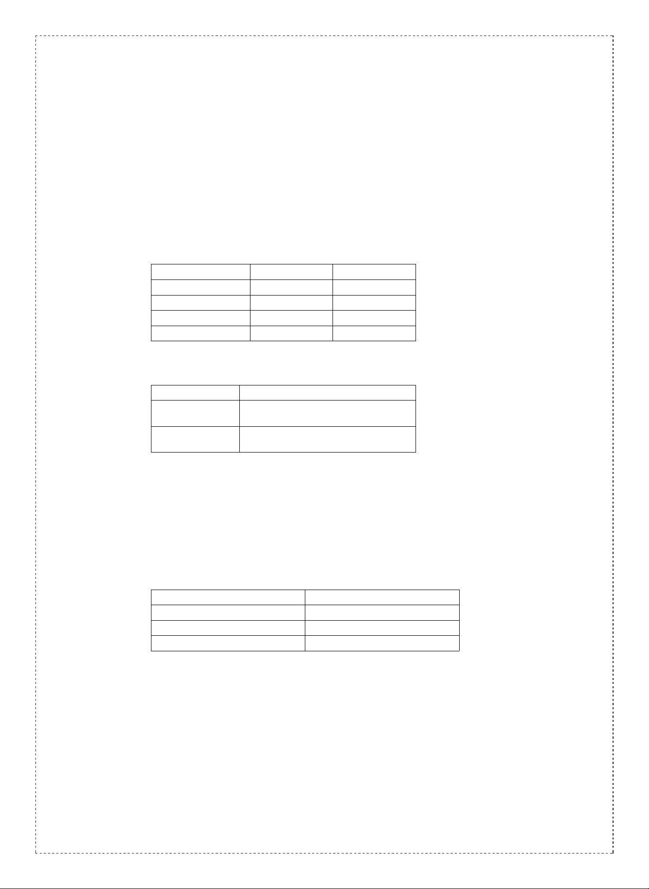
2) Set the DIP SW 1 and 2 as shown in the table below depending what unit
you are testing. Each u nit can b e test ed separat ely.
Unit to b e Tested DIP SW1 DIP SW2
Main Body OFF OFF
ADF ON OFF
FSU OFF ON
FSU ON ON
3) Set the DIP SW 4 depending on how many times you want to repeat the
oper ati on of th e uni t.
DIP SW4 How Many Times to Repeat
OFF
ON
4) T ur n ot h er D I P SW ( 3 , 5, 6 an d 9) OFF .
5) Turn the Power Switch ON.
–– The Ready Lamp blinks for a minute.
6) While the Ready Lamp is blinking, turn the DIP SW 8 OFF.
7) While the Ready Lamp is blinking, turn the DIP SW 7 OFF.
–– The unit begins to operate and you can monitor the process of the
operation by observing blinking lamps.
Status of Unit Status of Lamp
Scanner Head Pausing Ready Lamp ON
Scanner Head Moving Ready Lamp OFF
Optional Unit S elected Option Lamp ON
–– The Error Lamp turns ON and the diagnostic program fails on the following occasion.
The operation repeats until the
Power Switch turns OFF.
The operation repeats 480
times then, automatically stops.
2/7
• You made the wrong setting.
• You performed 6) and 7) after the Ready Lamp stopped blinking (i.e.
after 1 m inute passed sinc e the Po wer Sw itch tur ned ON ).
• You did not connect the optional unit with the scanner despite the
setting was made for the use of the unit.
Page 3

8) Turn the Power Switc h OFF to stop the diagnostic program. If you have
turned DIP SW 4 ON, the unit stops automatically after repeating the
operation 480 times, then, the Ready Lamp, the Option Lamp and the Error
Lamp blink in sequence.
B White Balance Test
1) Turn the DIP SW 5, 7 and 8 ON.
2) Turn the DIP SW 1,2,3,4,6 and 9 OFF.
3) Turn the Power Switch ON.
–– The Ready Lamp blinks for a minute.
4) While the Ready Lamp is blinking, turn the DIP SW 8 OFF.
5) While the Ready Lamp is blinking, turn the DIP SW 7 OFF.
–– The white b alance i s check ed, then , sca nning st arts wit h the sca nner
head remaining in the s ame posi tion. If a regu lar-siz ed origi nal is o n
the original table, a part icular part of the or iginal i mage is d isplaye d
repeatedly.
Then, you can check the operation of the scanner head and the image date
input circuit (mainly the analog signal processor).
–– Ready Lamp blinks during the operation.
–– The Error Lamp turns ON and the diagnostic progra m fails o n the
follow in g occa sion .
• You made the wrong setting.
• The performed 4) and 5) after the Ready Lamp stopped blinking (i.e.
after 1 m inute passed sinc e the Po wer Sw itch tur ned ON ).
8) Turn the Power Switc h OFF to stop the diagnostic program. If you have
connected the FSU, the diagnostic program checks the FSU.
C Shading waveform check
(The video input circuit waveform check)
Use this diagnostic program to check the video input circuit (an analog circuit).
Check the waveform obtained by the program to detect any failure in the circuit.
1) Turn the DIP SW 1,5,7 and 8 ON.
2) Turn the DIP SW 2, 3, 4, 6 and 9 OFF.
3) Turn the Power Switch ON.
–– The Ready Lamp blinks for a minute.
4) While the Ready Lamp is blinking, turn the DIP SW 8 OFF.
5) While the Ready Lamp is blinking, turn the DIP SW 7 OFF.
–– The waveform is now obtained for signals generated when all lamps are ON.
The diagnostic program fails with the Error Lamp ON if;
• You made the wrong DIP SW setting
3/7
Page 4

• You performed 4) and 5) while the Ready Lamp was not blinking
6) Turn the Power Switch OFF to stop the diagnostic program.
If you have connected the FSU, the diagnostic program checks the FS U.
The TP9 Waveform
Voltage (V)
2.6V
0.7V
8µs
Output Shading Waveform
Time (µs)
D Darknoise component waveform check
(The video input circuit waveform check)
Use this diagnostic program to check the video input circuit (an analog circuit).
Check the waveform obtained by the program to detect any failure in the circuit.
1) Turn the DIP SW 2, 5, 7 and 8 ON.
2) Turn the DIP SW 1, 3, 4, 6 and 9 OFF.
3) Turn the Power Switch ON.
–– The Ready Lamp blinks for a minute.
4) While the Ready Lamp is blinking, turn the DIP SW 8 OFF.
5) While the Ready Lamp is blinking, turn the DIP SW 7 OFF.
–– The waveform is now obtained for noises generated when all lamps are OFF.
The diagnostic program fails with the Error Lamp ON if;
• You made the wrong DIP SW setting.
• You performed 4) and 5) while the Ready Lamp was not blinking.
4/7
6) Turn the Power Switch OFF to stop the diagnostic program.
If you have connected the FSU, the diagnostic program checks the FS U.
Page 5

The TP10 Waveform
Voltage (V)
1.4V
0.7V
About 30ms
Enlarged
One wave-cycle consists of 256
small sawtooth patterns.
E Control Board Check
This diagnostic program checks :
• The device s such a s the I mage Proces sor, S CSI Co ntr oller and Gate A rray s
• Bus Lines on the Control Board
• Input/Output of signals in comm unications with the ADF
• Input/Output of signals in communications with the FSU
1) Turn the DIP SW 6, 7 and 8 ON.
2) Turn the DIP SW 1, 2, 3, 4, 5 and 9 OFF.
Time (ms)
3) Turn the Power Switch ON.
–– The Ready Lamp blinks for a minute.
4) While the Ready Lamp is blinking, turn the DIP SW 8 OFF.
5) While the Ready Lamp is blinking, turn the DIP SW 7 OFF.
–– The progr am simulates the scanning operation, creating automatically
particular image data (without actual scanning) and follows the steps
to process data until the data is sent to the interface unit.
–– If there is any defe ct in t he dev ices, the diagnost ic progra m detect s the
device that output unusual signal and shows you what device is
defec tiv e by c omb ina tio n s of b li nki ng la mps .
5/7
Page 6

During the operation, the Ready Lamp is blinking.
• If the operation finished successfully, the Ready Lamp stops
blinking and continues to be ON.
• If there is any problem:
1) The Er ror La mp bli n ks, an d then ,
2) Some of the Error, Ready and Opti on Lamps turn ON.
3) Some of the Error, Ready and Opti on Lamps turn ON in the
combination diff erent from above 2).
What lamps turns ON in steps 2) and 3) indicates the defect device.
Steps 1) to 3) are repeated until you finish the dia gnostic program.
–– The Error Lamp turns ON an d the diag nostic progra m fails o n the
follow in g occa sion .
• You made the wrong setting.
• You performed 4) and 5) after the Ready Lamp stopped blinking (i. e.
after 1 minute p assed since th e Power Switch t urned ON).
8) Turn the Power Switc h OFF to stop the diagnostic program. If you have
connected the FSU, the diagnostic program checks the control circuit of the
FSU.
6/7
Page 7

TROUBLE DISPLAY TABLE
LAMP CONDITION
ACTION 1 ACTION 2
BLINK A ERROR LAMP
R: READY LAMP ON
O: OPTION LAMP ON
E: ERROR LAMP ON
All lamps are off
E
E
E
E
E
E
O / E
O / E
O / E
O / E
O / E
O / E
R
R
R / E
R / E
R / E
R / O / E
R / O / E
R / O / E
R / O / E
ACTION 3
All lamps are off
E
O
O / E
R
R / E
R / O
E
O
O / E
R
R / E
R / O
E
O
E
O
O / E
E
O
O / E
R
7/7
DESCRIPTION
DIP SW trouble
B memory (IC22) databus trouble
C memory (IC27) databus trouble
Z memory (IC23) databus trouble
S memory (IC21) databus trouble
LL memory (IC35) databus trouble
LH memory (IC30) databus trouble
B memory (IC22) addressbus trouble
C memory (IC27) addressbus trouble
Z memory (IC23) addressbus trouble
S memory (IC21) addressbus trouble
LL memory (IC35) addressbus trouble
LH memory (IC30) addressbus trouble
Data transmission trouble from L memory (IC30, 35) to S (IC21) memory
Data transmission trouble from L memory (IC30, 35) to FIFO (IC38) memory
GATE ARRAY 1 (IC29) trouble
GATE ARRAY 2 (IC34) trouble
SCSI controller (IC36) trouble
LUT memory (IC34) trouble
EVEN memory (IC33) trouble
ODD memory (IC37) trouble
FIFO memory (IC38) trouble
 Loading...