

Page 1
Date: May. 11, 1995
COLOR IMAGE SCANNER : JX-330
No. : CX-170
CHANGE IN CONTROL PWB AND ROM TO
IMPROVE FUNCTION
1.Model name: JX330/M/P
2.General: Changes have been carried out in the control PWB, and in the ROM to improve function
since the first lot of shipment.
The changes carried out up to date are described below.
3.Description: 1) Control, and PS PWB
➀ Alleviating problems with vertical streaking at even spaces during high quality
imaging (greater than 600 dpi) transparance/reflectance reading operations, see
examples.
➁ Supplies power to the terminator for laptop computers.
➂ Adding and eliminating parts in accordance with the change in ROM.
Changes have been implemented on new PWB produced after mid-September
production which correspond to the above problem [For USA: DUNTK7864XCZA
(120V), for Europe: DUNTK7868XCZA (200V)].
The changes listed below should be carried out on only old PWB [For USA:
DUNTK7864XCZZ (120V), for Europe: DUNTK7868XCZZ (200V)].
(Refer to Supplement-1)
2) ROM
After the changes described in ➀ above for the control, and PS PWB have been
carried out on old PWB [For USA: DUNTK7864XCZZ (120V), for Europe:
DUNTK7868XCZZ (200V)], the ROM should be changed to the newest version (S081I).
(Refer to Supplement-2)
Even spaced, vertical lines during high
1
resolution (more than 6000 Pi) transparent/
reflection reading operations.
Even spaced, vertical lines.
SHARP CORPORATION Printer and Scanner Division
1/8
Orange
CS
Page 2
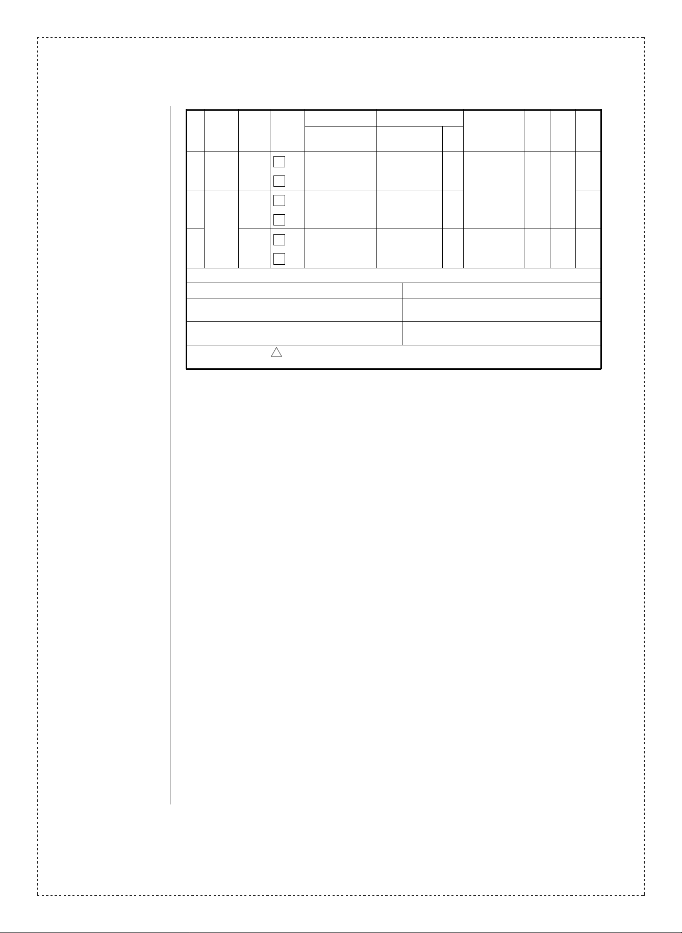
Ref.
No.
Model
name
Version P/G No.
Current parts New parts
Parts code Parts code
Price
rank
Parts name
Effec-
tive
time
Inter-
change-
ability
Note
1 JX330 U.S.A
2
JX330/
M/P
3 All
<Interchange>
1. Interchangeable. 4. Not interchangeable.
2. C urr e nt t y pe c a n be u s ed i n p la ce of new t y pe .
New ty pe cann ot be us ed i n place of curr ent type .
3. C urre nt ty pe cann ot be used i n place of new ty pe.
New t y pe c a n be u sed in p la c e of c u rr en t ty p e.
Parts marked with “ ” is important for maintaining the safety of the set. Be sure to replace these parts with
specified ones for maintaining the safety and performance of the set.
Except
U.S.A
1 -503
4 -901
1 -503
5 -901
4 -196
5 -198
!
DUNTK7864XCZZ DUNTK7864XCZA VF
Control, and PS
PWB
DUNTK7868XCZZ DUNTK7868XCZA VF
VHI27020S081E VHI27020S081I GN ROM ’94/12 3
5. Interchangeable if replaced with same types of
relate d parts in use .
6. Others .
’94/9 4
8/8
Page 3
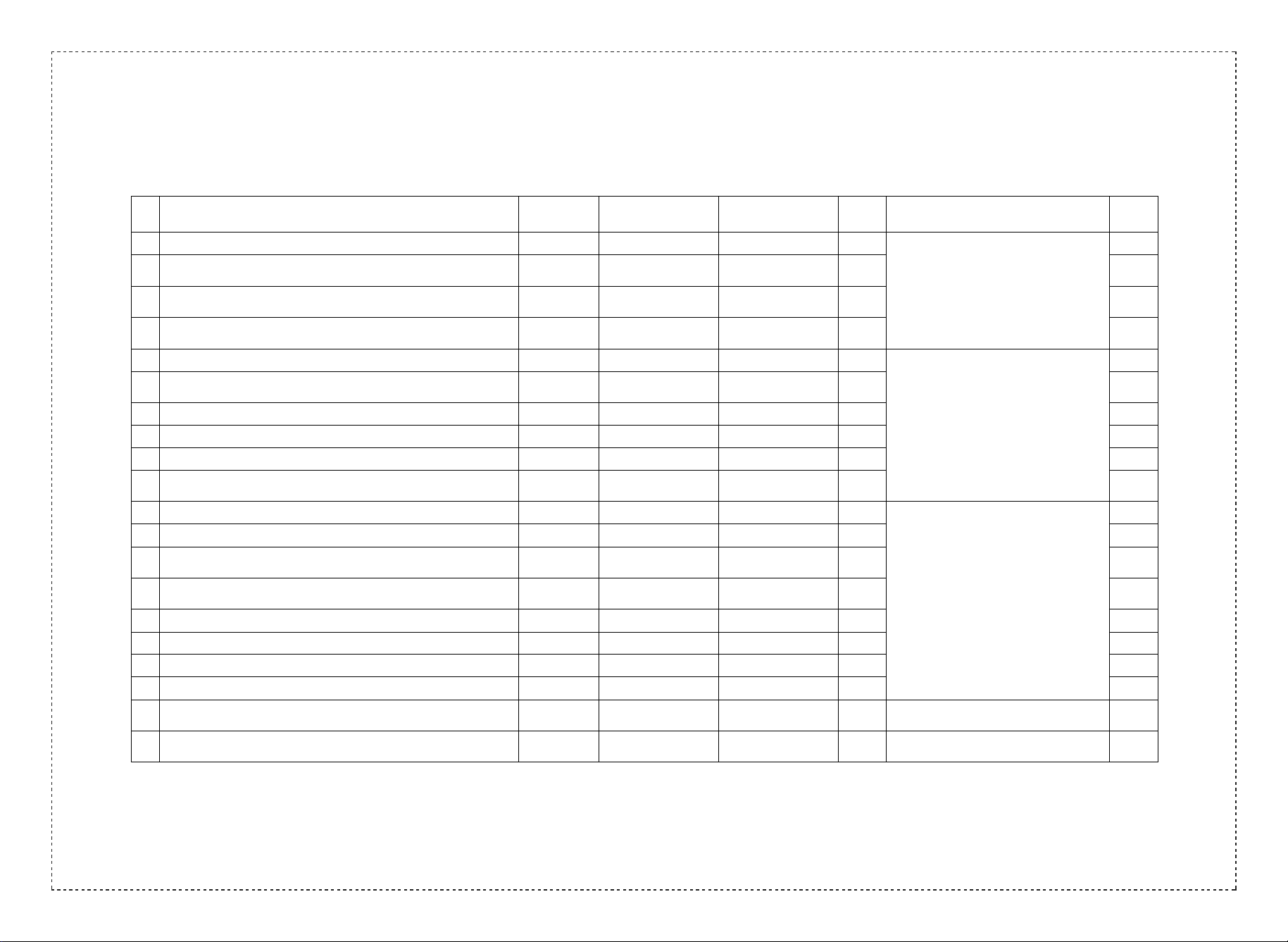
2/8
(Supplementary Table 1)
Changes in the control and PS circuit boards (refer to the parts location diagram and the circuit diagrams for details.)
No. Change description
1 R178 has been discontinued. Discontinued VRS-TS2AD560J — 5-426
A jumper line (JP6) has been added between the No. 12 pin of IC42
2
and L37 (below).
A jumper line (JP7) has been added between the No. 11 pin of IC42
3
and L36 (left).
A jumper line (JP8) has been added between the No. 10 pin and the
4
No. 13 pin of IC42.
5 Change in multiplier of R135 from 220Ω to 330Ω. Change VRS-TS2AD221J VRS-TS2AD331J 5-387
A resistor (560Ω) has been added between the No. 1 pin of IC25 and
6
the No. 28 pin of IC24.
7 The capacity of C115 has been changed from 47pF to 0.1µF. Changed VCCCTV1HH470J VCKYTV1EF1042 5-145
8 C131 has been discontinued. Discontinued No description on P/G — 59 R176 has been discontinued. Discontinued VRS-TS2AD221J — 5-424
A jumper line (JP4) has been added between the No. 2 pin and the
10
No. 7 pin of IC42.
11 The capacity of C70 has been changed from 120 pF to 82 pF. Changed VCCCTV1HH470J VCCCTV1HH820J 5-101
The capacity of C79 has been changed from 82 pF to 56 pF.
12
A resistor (330Ω) has been added between the No. 12 pin of IC32
13
and the No. 23 pin of IC26.
A resistor (330Ω) has been added between the No. 10 pin of IC32
14
and the No. 23 pin of IC26.
15 The capacity of C116 has been changed from 47 pF to 120 pF. Changed VCCCTV1HH470J VCCCTV1HH121J 5-146
16 A diode (EK04) has been added between VCC and C128+. Added — VHDEK04////-1 517 A line has negative cut at the No. 38 pin of CN9 and CN10. Negative cut — — 5-
A fuse (ICPN25) has been added to the No. 31 cut section.
18
A jumper line (JP5) has been added between the No. 103 pin
19
(through-hole) of GA1 and the No. 5 pin of IC42.
A capacitor (100 pF) has been added between the No. 102 pin
20
(through-hole) of GA1 and the No. 7 pin (GND) of IC42.
Type of
change
Added — — 5- JP6
Added — — 5- JP7
Added — — 5- JP8
Added — VRD-HT2EY561J 5-
Added — — 5- JP4
Changed VCCCTV1HH470J VCCCTV1HH560J 5-110
Added — VRD-HT2EY331J 5-
Added — VRD-HT2EY331J 5-
Added — VHVICPN25//-1 5Added — — 5- From 1994 mid-October production. JP5
Added — VCKYPU1HB101K 5-
Old parts code New parts code P/G No. Effective time Notes
From 1994 mid-August production.
From 1994 mid-September production.
From 1994 mid-September production.
From 1994 mid-November production.
Page 4

(Supplementary Table 2)
Changes in the ROM.
ROM version Change description Old parts code New parts code Effective time Notes
S081E
S081F
S081G
S081H
S081I
Improvement of poor image quality during operations at low temperatures.
Correction of ADF reading errors.
Correction of darkness changes in the final reading section during MTF
compensation reading operations.
Correction of reading area misalignment during ADF reading operations.
Addition of an error resetting function for when the ADF cover is opened
while the original copy is being discharged.
Improvement of resolution for Y-axis reading during low speed, gray scale
reading operations (correction of feed scanning jags).
Alleviation of problems with vertical lines in the new pattern PWB
(DUNTK7864XCZA/DUNTK7868XCZA).
Addition of a service diagnostics.
Reduction of time required for white balance operations.
Addition of an ADF open cover detection processing function during
scanning preparations (the fluorescent light warm-up period).
Increase of the reading capacity (number of pages) for ADF reading
operations.
Correction of vertical lines in the display (red/blue/green) during 75DPI, A4
reading operations (except for model JX-330M).
Correction of display malfunctions (total blackouts) during negative/positive
change operations (except for model JX-330M).
VHI27020S081D VHI27020S081E From 1994 mid-August production. T/R CX-160
VHI27020S081E VHI27020S081F From 1994 mid October production.
VHI27020S081F VHI27020S081G From 1994 mid-October production.
VHI27020S081G VHI27020S081H From 1994 mid-December production.
VHI27020S081H VHI27020S081I From 1994 mid-December production.
3/8
Page 5

Page 6

Page 7

Page 8

 Loading...