

Page 1

COLOR IMAGE SCANNER : JX-610
PARTS ADDITION/ELIMINATION
A section of the explanation given in Technical Report no. CX-139, issued on September
10, 1993 was unclear and difficult to understand. This revised version of the technical
report is therefore being issued, and we would like to ask that it be used to replace the
first version.
Date: Mar. 3, 1994
REVISED
No. : CX-139 (R)
1. ROM changes
1. Model name: JX-610
2. General: ROM has been changed to correct bugs in the MODE SELECT command and data
changes in Inquiry (for when the LUN ≠ 0)
3. Effective time: July, 1993.
2. Making EPROM into MASK ROM
1. Model name: JX-610
2. General: To improve productivity, EPROM has been changed to mask ROM.
3. Effective time: April, 1993.
3. Addition of programming manual
1. Model name: JX-610
2. Effective time: December, 1992.
SHARP CORPORATION Printer and Scanner Division
1/9
Orange
C
Page 2

4. Parts changes for F marks and improved productivity
1. Model name: JX-610
2. General: For F marks and improved productivity, parts have been added to and removed from
control boards A and B and the ADC board.
3. Description: Please see the parts diagrams for details.
ADC Board 100V type (USA, Canada)
R78 VRD-RC2EY105J (Resistor 1MΩ)
D1 VHDDS1588L2-1 (Diode)
C76 RC-K 1H105XCZZ (Con denser 105)
R74 VRD-RC2EY103J (Resistor
10KΩ)
AINPEAK, 5VREF, A0S
VRD-HT2EY000J (Resistor 0Ω)
VR2 200Ω → 100Ω (RVR-M1210QCN3)
ADC Board 200V type (Europe, U.Kindom, Australia, SRH)
R78 VRD-RC2EY105J (Resistor 1MΩ)
D1 VHDDS1588L2-1 (Diode)
C76 RC-K 1H105XCZZ (Con denser 105)
R74 VRD-RC2EY103J (Resistor
10kΩ)
TR5 VS2SC1214//-1 (Transistor)
L8, 9 Non- m ounted parts
L7 VRD-RC2EY000J
(Resistor 0Ω)
R75, 76
VRD-RC2EY751J
(Resistor 750Ω)
IC5, 6 VHIAD811AN/-1
(Video Op Amp)
TR5 VS2SC1214//-1 (Transistor)
L8, 9 Non- m ounted parts
L7 RCILZ7020SCZZ (Ferrite beads)
2/9
AINPEAK, 5YREF, A0S
VRD-2EY000J (Resistor 0Ω)
2 VR2 200Ω → 100Ω
R75, 76 VRD-RC2EY751J
(Resistor 750Ω)
IC5, 6 VHIAD811AN-1
(Video Op Amp)
Page 3
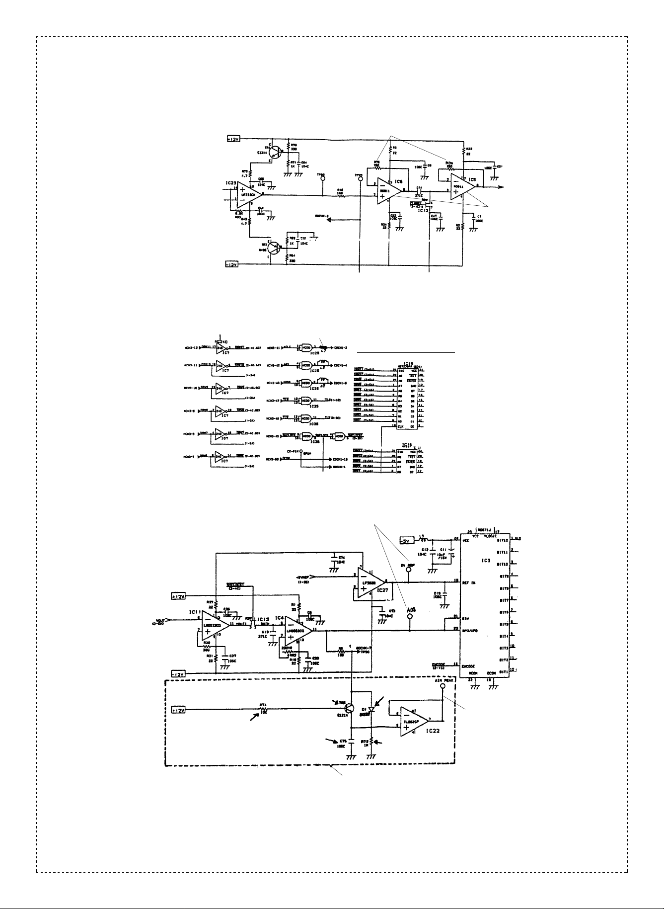
Circuit diagram of the ACD circuit board (1/3)
Circuit diagram of the ACD circuit board (2/3)
Added 0Ω resistor (L 7), VRD-RC2EY000J (100V type).
Added Ferrite beads (L 7), RCILZ7020SCZZ (200V type).
Added 750 resistor (R 75.76).
LH0033GC has been
changed to AD811AN
(IC 5, 6).
L 8 and L9 are not installed.
Circuit diagram of the ACD circuit board (3/3)
Added transistor VS2SC1214//-1.
Added 10 KΩ resistor VRD-RC2EY103J.
Added 1µF capacitor RC-KIH105XCZZ.
Added 0Ω resistor (L 7), VRD-RC2EY000J.
Added diode
VHDDS1588L2-1.
Added 0Ω resistor
VRD-RC2EY000J.
Added 1MΩ resistor
VRD-RC2EY105J.
Added adjustment circuit.
3/9
Page 4

Control A circuit board, 100V series (bound for the USA and Canada)
[Parts location diagram]
Added 0Ω resistor VRD-RC2EY000J (L 25).
[Circuit diagram]
Added 0Ω resistor VRD-RC2EY000J (L 25).
Control B circuit board, 100V series (bound for the USA and Canada)
[Parts location diagram]
Added 0Ω resistor VRD-RC2EY000J (L1 to 4).
[Circuit diagram]
Added 0Ω resistor
VRD-RC2EY000J (L1 to 4).
4/9
Page 5

Control B circuit board, 200V series (bound for Europe, the United Kingdom and Australia SRH)
[Parts location diagram]
Added ferrite beads (4 x RCILZ7020SCZZ) (L1 to L4).
[Circuit diagram]
Added ferrite beads (4 x RCILZ7020SCZZ) (L1 to L4).
5/9
Page 6

5. Parts changes for change to a gate array
1. Model name: JX-610
2. General: Parts have been added to and removed from control board B for changing to a gate
array.
3. Description: Please see the diagrams below.
(Before changes)
(After changes)
QCNCM7031SC9F
Area changed (See parts code list)
Gate array VHIF254034PJ1 (IC86)
QCNCM7031SC9F
6/9
VHILH534F57-1
(S001B)
VHI531024J214
(S051A)
QPIN2010SCZZ
S011*
Lot display label
Page 7

Circuit diagram.
(Old)
6-2. CCD Data controller / main scanning direction MTF correction circuit.
(New)
The parts contained within the dotted line have been discontinued, and
replaced with a gate array (VHIF254030PJ1 IC86). A diagram of the
circuit after the change is shown below.
Added gate array (VHIF254034PJ1).
2:Effective time From 1993 August production.
7/9
Page 8

Ref.
No.
1
2
3
4
Model
name
JX610
Version P/G No.
USA
Except
USA
15 -147
15 -147
16 -81
All
16 -110
Canada
USA
Canada
U.Kingdom
Europe
Australia
SRH
14 -
17 -
17 -
17 -
17 -
17 -
17 -
All
17 -
17 -
17 -
17 -
Current parts New parts
Parts code Parts code
Price
rank
VHI27512S101F VHI27512S101I BF
VHI27512S101H VHI27512S101I BF
VHI27010S051A VHI531024J214 AU
VHI27040S001A VHILH534F74-1 AX
— TINSE7101XCZZ BN
— VRD-RC2EY000J AA
VRD-RC2EY000J RCILZ7020SCZZ
— RC-K1H105XCZZ AB
— VRD-RC2EY103J AA
— VRD-RC2EY000J AA
— VRD-RC2EY105J AA
— VRD-RC2EY751J AA
— VHDDS1588L2-1 AB
RC-K1H105XCZZ VCKYPU50V271K AA
PSPAY7052XCZZ — —
Parts name
EP-ROM (IC53)
EP-ROM (IC53)
MASK ROM
(IC9)
MASK ROM
(IC37)
Programming
manual
Resistor
(1/4W 0Ω ±5%)
Ferrite beads
Condenser
(50WV 1µF)
Resistor
(1/4W 10KΩ ±5%)
Resistor
(1/4W 0Ω ±5%)
Resistor
(1/4W 1MΩ ±5%)
Resistor
(1/4W 750Ω ±5%)
Diode
(DS1588L2)
Condenser
(50WV 270pF)
Spacer
Effec-
Inter-
tive
change-
time
ability
’93/7 3
’93/7 3
’93/4 1
’93/4 1
’92/12 6
’93/3 6
’93/3 6
’93/3 6
’93/3 6
’93/3 6
’93/3 6
’93/3 6
’93/3 6
’93/3 6
’93/3 6
Note
L7
L7
C76
R74
Pin
PEAK
5VREF
A0S
R78
R75,
76
D1
C13,
14
IC5, 6
8/9
USA
Canada
U.Kingdom
Europe
Australia
SRH
5 All
17 -
17 -
15 -
16 -
16 -
16 -117
16 -126
16 -142
16 -124
16 -128
— VS2SC1214//-1 AD
VHILH0033CG-1 VHIAD811AN/-1 BD
— VRD-RC2EY000J AA
— VRD-RC2EY000J AA
VRD-RC2EY000J RCILZ7020SCZZ
VHIMB7132HS01 — —
VHIXC1736AS11 — —
VHIXC1736AS21 — —
VHIXC2018-050 — —
VHIXC3030-070 — —
Transistor
(2SC1214)
IC (AD811AN)
Resistor
(1/4W 0Ω ±5%)
Resistor
(1/4W 0Ω ±5%)
Ferrite beads
IC
(MB7132HS01)
IC
(XC1736AS11)
IC
(XC1736AS21)
IC (XC2018-050)
IC (XC3030-070)
’93/3 6
’93/3 1
’93/3 6
’93/3 6
’93/3 6
’93/8 6
’93/8 6
’93/8 6
’93/8 6
TR5
IC5, 6
L25
L1~4
L1~4
IC43
IC50
IC63
IC49
’93/8 6 IC51
Page 9

Ref.
Model
No.
name
5 JX-610 All
Version P/G No.
16 -123
16 -127
16 -
16 -168
16 -170
16 -115
Current parts New parts
Parts code Parts code
Price
rank
QSOCZE068HCZZ — —
— VHIF254034PJ1 AZ
VRD-RC2EY562J — —
VHIT7406///-C — —
Parts name
IC socket (68pim)
IC (F254034PJ1)
Resistor
(1/4W 5.6KΩ ±5%)
IC (T7406)
Effective
time
’93/8 6
’93/8 6 IC86
’93/8 6 R2, 4
’93/8 6 IC42
<Interchange>
1. Interchangeable. 4. Not interchangeable.
2. C urr e nt t y pe c a n be u s ed i n p la ce of new t ype .
New ty pe cann ot be us ed i n place of curr ent type .
3. C urre nt ty pe cann ot be used i n place of new ty pe.
New t y pe c a n be u sed in p la c e of c u rr en t ty p e.
5. Interchangeable if replaced with same types of
relate d parts in use .
6. Others .
Parts marked with “ ” is important for maintaining the safety of the set. Be sure to replace these parts with
specified ones for maintaining the safety and performance of the set.
Interchangeability
Note
IC49,
51
9/9
 Loading...