


CD-M8000W/CP-M8000
SERVICE MANUAL
No. S4228CDM8000W
MINI COMPONENT SYSTEM
MODEL CD-M8000W
SPEAKER SYSTEM
MODEL CP-M8000
• In the interests of user-safety the set should be restored to its original condition and only parts identical to those specified be used.
CONTENTS |
|
|
Page |
SAFETY PRECAUTION FOR SERVICE MANUAL ........................................................................................................... |
2 |
VOLTAGE SELECTION ..................................................................................................................................................... |
2 |
AC POWER SUPPLY CORD AND AC PLUG ADAPTOR ................................................................................................. |
2 |
SPECIFICATIONS ............................................................................................................................................................. |
3 |
NAMES OF PARTS ........................................................................................................................................................... |
4 |
DISASSEMBLY .................................................................................................................................................................. |
6 |
REMOVING AND REINSTALLING THE MAIN PARTS ..................................................................................................... |
9 |
ADJUSTMENT ................................................................................................................................................................. |
10 |
NOTES ON SCHEMATIC DIAGRAM .............................................................................................................................. |
14 |
TYPES OF TRANSISTOR AND LED ............................................................................................................................... |
14 |
BLOCK DIAGRAM ........................................................................................................................................................... |
15 |
SCHEMATIC DIAGRAM / WIRING SIDE OF P.W.BOARD ............................................................................................. |
18 |
VOLTAGE ........................................................................................................................................................................ |
36 |
WAVEFORMS OF CD CIRCUIT ...................................................................................................................................... |
37 |
TROUBLESHOOTING ..................................................................................................................................................... |
38 |
FUNCTION TABLE OF IC ................................................................................................................................................ |
42 |
FL DISPLAY ..................................................................................................................................................................... |
50 |
REPLACEMENT PARTS LIST/EXPLODED VIEW |
|
This document has been published to be used
SHARP CORPORATION– 1 – |
for after sales service only. |
|
|
|
The contents are subject to change without notice. |
CD-M8000W/CP-M8000
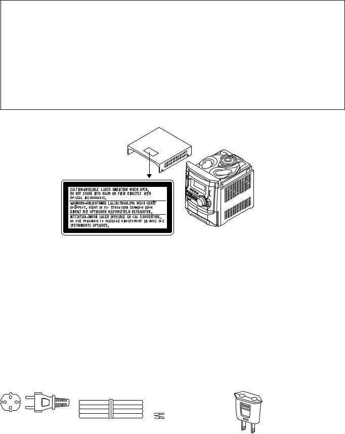
SAFETY PRECAUTION FOR SERVICE MANUAL
WARNINGS
THE AEL (ACCESSIBLE EMISSION LEVEL) OF THE LASER POWER OUTPUT IS LESS THAN CLASS 1 BUT THE LASER COMPONENT IS CAPABLE OF EMITTING RADIATION EXCEEDING THE LIMIT FOR CLASS 1. THEREFORE IT IS IMPORTANT THAT THE FOLLOWING PRECAUTIONS ARE OBSERVED DURING SERVICING TO PROTECT YOUR EYES AGAINST EXPOSURE TO THE LASER BEAM.
1-WHEN THE CABINET IS REMOVED, THE POWER IS TURNED ON WITHOUT A COMPACT DISC IN POSITION AND THE PICKUP IS ON THE OUTER EDGE THE LASER WILL LIGHT FOR SEVERAL SECONDS TO DETECT A DISC. DO NOT LOOK INTO THE PICKUP LENS.
2-THE LASER POWER OUTPUT OF THE PICKUP UNIT AND REPLACEMENT SERVICE PARTS ARE ALL FACTORY PRESET BEFORE SHIPMENT.
DO NOT ATTEMPT TO READJUST THE LASER PICKUP UNIT DURING REPLACEMENT OR SERVICING. 3-UNDER NO CIRCUMSTANCES STARE INTO THE PICKUP LENS AT ANY TIME.
4-CAUTION-USE OF CONTROLS OR ADJUSTMENTS, OR PERFORMANCE OF PROCEDURES OTHER THAN THOSE SPECIFIED HEREIN MAY RESULT IN HAZARDOUS RADIATION EXPOSURE.
Laser Diode Properties
Material: GaAIAs
Wavelength: 780 nm
Emission Duration: continuous
Laser Output: max. 0.6 mW
VOLTAGE SELECTION
Before operating the unit on mains, check the preset voltage. If the voltage is different from your local voltage, adjust the voltage as follows.
Turn the selector with a screwdriver until the appropriate voltage number appears in the window (110 V, 127 V, 220 V or 230 V-240 V AC).
AC POWER SUPPLY CORD AND AC PLUG ADAPTOR
QACCE0014AW00 |
|
QPLGA0005AWZZ |
||||
|
|
|||||
|
|
|
|
|
|
|
|
|
|
|
|
|
|
|
|
|
|
|
|
|
|
|
|
|
|
|
|
|
|
|
|
|
|
|
|
|
|
|
|
|
|
|
|
|
|
|
|
|
|
|
|
|
|
|
|
– 2 –

CD-M8000W/CP-M8000
FOR A COMPLETE DESCRIPTION OF THE OPERATION OF THIS UNIT, PLEASE REFER TO THE OPERATION MANUAL.
SPECIFICATIONS
CD-M8000W |
|
CP-M8000 |
|
|
|
 General
Power source |
AC 110/127/220/230 - 240 V, 50/60 Hz |
Power consumption |
180 W |
|
|
Dimensions |
Width: 270 mm (10-5/8") |
|
Height: 330 mm (13") |
|
Depth: 360 mm (14-3/16") |
Weight |
11.7 kg (25.7 lbs.) |
|
|
 Amplifier
Output power |
MPO: 860 W (430 W + 430 W) (10 % T.H.D.) |
|
RMS: 500 W (250 W + 250 W) (10 % T.H.D.) |
|
RMS: 360 W (180 W + 180 W) (0.9 % T.H.D.) |
Output terminals |
Speakers: 6 ohms |
|
Headphones: 16 - 50 ohms (recommended: 32 ohms) |
|
|
Input terminals |
Video/Auxiliary (audio signal): 500 mV/47 k ohms |
|
Microphone: 1 mV/600 ohms |
|
|
 CD player
Type |
3-disc multi-play compact disc player |
Signal readout |
Non-contact, 3-beam semiconductor laser pickup |
D/A converter |
1-bit D/A converter |
|
|
Frequency response |
20 - 20,000 Hz |
|
|
Dynamic range |
90 dB (1 kHz) |
|
|
 Tuner
Tuner
Frequency range |
FM: 88 - 108 MHz |
|
AM: 531 - 1,602 kHz |
|
|
 Cassette deck
Frequency response |
50 - 14,000 Hz (Normal tape) |
Signal/noise ratio |
55 dB (TAPE 1, playback) |
|
50 dB (TAPE 2, recording/playback) |
|
|
Wow and flutter |
0.3 % (WRMS) |
|
|
Type |
4-way type speaker system |
|
Super Tweeter |
|
10 cm (4") Tweeter |
|
10 cm (4") Midrange |
|
25 cm (10") Woofer |
|
|
Maximum input power |
500 W |
(Total) |
|
Rated input power |
250 W |
(Total) |
|
Impedance |
6 ohms |
|
|
Dimensions |
Width: 465 mm (18-5/16") |
|
Height: 330 mm (13") |
|
Depth: 373 mm (14-11/16") |
Weight |
10.1 kg (22.2 lbs.)/each |
|
|
Specifications for this model are subject to change without prior notice.
– 3 –
CD-M8000W/CP-M8000
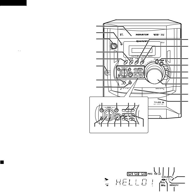
NAMES OF PARTS
CD-M8000W
 Front panel
1.Disc Tray
2.Timer Set Indicator
3.On/Stand-by Button
4.Tuner (Band) Button
5.CD Button
6.Headphone Socket
7.Microphone Level Control
8.Microphone Socket
9. Tape (1 2) Button
10.Video/Auxiliary Button
11.Equaliser Mode Select Button
12.Monster Bass/Demo Mode Button (with Indicator)
13.Disc Tray Open/Close Button
14.Disc Skip Button
15.Volume Control
16.Tape 1 Cassette Compartment
17.Tape 2 Cassette Compartment
18.CD Track Down or Fast Reverse, Tape 2 Fast Wind, Tuner Preset Down Button
19.CD Track Up or Fast Forward, Tape 2 Fast Wind, Tuner Preset Up Button
20.Clock Button
21.Timer/Sleep Button
22.Tape 2 Reverse Mode Select Button
23.Tape 2 Reverse Play Button (with Indicator)
24.CD Play or Repeat, Tape 1 Play,
Tape 2 Forward Play Button(with Indicator)
25.CD or Tape Stop Button (with Indicator)
26.Tuning and Time Down Button
27.Memory/Set Button
28.Tape 2 Record Pause Button
29.Tuning and Time Up Button
1 |
|
2 |
|
3 |
9 |
|
10 |
4 |
|
|
5 |
11 |
|
6 |
12 |
|
|
13 |
|
7 |
14 |
|
15 |
||
8 |
||
|
|
|
|
16 |
18 |
19 |
20 21 |
17 |
22 23 24 25 26 27 28 29
Display
1.CD Pause Indicator
2.Disc Number Indicators
3.Tape 2 Record Indicator
4.FM Stereo Mode Indicator
5.FM Stereo Receiving Indicator
6.Timer Play Indicator
7.Sleep Indicator
8.Timer Recording Indicator
9.CD Play Indicator
10.CD Repeat Play Indicator
11.Karaoke Mode Indicator
12.Tape Reverse Mode Indicator
13.Tape 2 Reverse Play Indicator
14.Tape 1 Play or Tape 2 Forward Play Indicator
15.Memory Indicator
1 |
2 |
3 |
4 |
5 6 |
7 |
8 |
|
||||||
9 |
|
|
|
|
|
|
|
|
|
|
|
|
11 |
|
|
|
|
|
|
|
|
|
|
|
|
||
|
|
|
|
|
|
|
|
|
|
|
|
||
|
|
|
|
|
|
|
|
|
|
|
|
||
|
|
|
|
|
|
|
|
|
|
|
|
12 |
|
|
|
|
|
|
|
|
|
|
|
|
|
||
10 |
|
|
|
|
|
|
|
|
|
|
|
|
|
|
|
|
|
|
|
|
|
|
|
|
|
|
|
|
|
|
|
|
|
|
|
|
|
|
|
|
|
|
|
|
|
|
|
|
|
|
|
13 |
14 |
15 |
|
– 4 –
CD-M8000W/CP-M8000
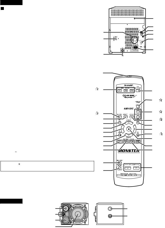
CD-M8000W
Rear panel
1.Cooling Fan
2.AC Voltage Selector
3.AC Power Lead
4.Transport Screw
5.FM 75 Ohms Aerial Terminal
6. |
FM Aerial Earth Terminal |
1 |
7. |
AM Loop Aerial Socket |
|
8. |
Span Selector Switch |
2 |
9. |
Video/Auxiliary (Audio Signal) Input Sockets |
|
10. Speaker Terminals |
|
|
Note: |
|
|
This product is equipped with a cooling fan inside, which begins to run at a specified |
3 |
|
volume level for better heat radiation. |
||
4
5 

 6
6 

 7
7
8


 9
9 


 10
10

 Remote control
1.Remote Control Transmitter
2.Disc Number Select Buttons
3.CD Random Button
4.CD Memory Button
5.CD Track Up or Fast Forward, Tape 2 Fast Wind Button
6.Tuner Preset Up Button
7.Tape 2 Reverse Play Button
8.Tape 2 Record Pause Button
9.Tuner Preset Down Button
10.CD Button
11.Tuner (Band) Button
12.Equaliser Mode Select Button
13.Monster Bass Button
14.On/Stand-by Button
15.Karaoke Mode Button
16.Echo Level Up and Down Buttons
17.CD Clear Button
18.CD Track Down or Fast Reverse, Tape 2 Fast Wind Button
19.CD Play or Repeat, Tape 1 Play, Tape 2 Forward Play Button
20.CD Pause Button
21.CD or Tape Stop Button
22.Video/Auxiliary Button
23. |
Tape (1 2) Button |
24. |
Volume Up and Down Buttons |
Buttons with " " mark in the illustration can be operated on the remote control only.
CP-M8000
1. |
Tweeter |
1 |
2. |
Super Tweeter |
2 |
3. |
Midrange |
|
4. Woofer |
3 |
|
5. |
Bass Reflex Duct |
|
6. |
Speaker Terminals |
4 |
|
|
|
1 |
|
|
2 |
14 |
|
|
15 |
|
3 |
16 |
|
|
||
4 |
17 |
|
5 |
18 |
|
6 |
19 |
|
7 |
||
20 |
||
8 |
||
21 |
||
9 |
||
22 |
||
10 |
||
11 |
23 |
|
12 |
|
 24
24
13
5
6
– 5 –
CD-M8000W/CP-M8000
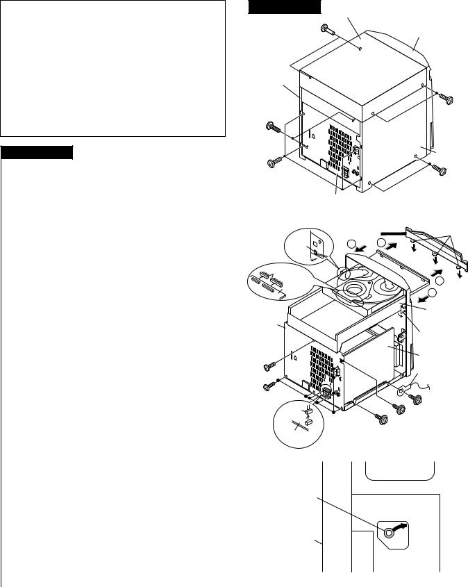
DISASSEMBLY
Caution on Disassembly
Follow the below-mentioned notes when disassembling the unit and reassembling it, to keep it safe and ensure excellent performance:
1.Take cassette tape and compact disc out of the unit.
2.Be sure to remove the power supply plug from the wall outlet before starting to disassemble the unit.
3.Take off nylon bands or wire holders where they need to be removed when disassembling the unit. After servicing the unit, be sure to rearrange the leads where they were before disassembling.
4.Take sufficient care on static electricity of integrated circuits and other circuits when servicing.
CD-M8000W
STEP |
REMOVAL |
|
PROCEDURE |
|
|
|
FIGURE |
|
|
|
|
|
|
|
|
|
|
1 |
Top Cabinet |
1. |
Screw ....................... |
(A1) x4 |
6-1 |
|||
2 |
Side Panel |
1. |
Screw ....................... |
(B1) x8 |
6-1 |
|||
|
(Left/Right) |
|
|
|
|
|
|
|
|
|
|
|
|
|
|
|
|
3 |
CD Player Unit/ |
1. |
Turn on the power supply, |
... |
|
6-2 |
||
|
CD Tray Cover |
|
open the loading tray, take out |
|
|
|||
|
|
|
the CD tray cover, and close. |
|
||||
|
|
|
(Note 1) |
|
|
|
|
|
|
|
2. |
Screw ....................... |
(C1) x1 |
|
|||
|
|
3. |
Hook ......................... |
(C2) x3 |
|
|||
|
|
4. |
Hook ......................... |
(C3) x2 |
|
|||
|
|
5. |
Socket ...................... |
(C4) x2 |
|
|||
4 |
Rear Panel with |
1. |
Screw ....................... |
(D1) x9 |
6-2 |
|||
|
Fan Motor |
2. |
Socket ...................... |
(D2) x1 |
|
|||
|
|
|
|
|
|
|
|
|
5 |
Main PWB |
1. |
Screw ....................... |
(E1) x2 |
6-2 |
|||
|
|
2. |
Flat Cable ................ |
(E2) x1 |
7-1 |
|||
|
|
3. |
Socket ...................... |
(E3) x4 |
|
|||
|
|
|
|
|
|
|
|
|
6 |
Amp. PWB |
1. |
Screw ....................... |
(F1) x6 |
7-2 |
|||
|
|
2. |
Socket ...................... |
(F2) x4 |
|
|||
|
|
3. |
PWB Holder ............. |
(F3) x5 |
|
|||
|
|
4. |
Flat Wire ................... |
(F4) x1 |
|
|||
|
|
|
|
|
|
|
|
|
7 |
Front Panel |
1. |
Screw ....................... |
(G1) x3 |
7-2 |
|||
|
|
2. |
Hook ......................... |
(G2) x2 |
7-1 |
|||
|
|
|
|
|
|
|
|
|
8 |
Mic PWB |
1. |
Screw ....................... |
(H1) x2 |
7-3 |
|||
|
|
2.Tip ............................. |
(H2) x1 |
|
||||
9 |
Display PWB |
1. |
Knob .......................... |
(J1) x1 |
7-3 |
|||
|
|
2. |
Screw ...................... |
(J2) x15 |
|
|||
|
|
3. |
Flat Cable ................. |
(J3) x1 |
|
|||
|
|
|
|
|
|
|
|
|
10 |
Tape Mechanism |
1. |
Open the cassette holder. |
7-3 |
||||
|
|
2. |
Screw ....................... |
(K1) x5 |
|
|||
|
|
|
|
|
|
|
|
|
11 |
Headphones PWB |
1. |
Screw ....................... |
(L1) x1 |
7-3 |
|||
12 |
Turntable |
1. Hook ........................ |
(M1) x2 |
7-4 |
||||
|
|
2. |
Cover ...................... |
(M2) x1 |
|
|||
|
|
|
|
|
|
|
|
|
13 |
Loading Tray |
1. |
Turn fully the lock lever in the . |
6-3 |
||||
|
|
|
arrow direction |
|
|
|
|
|
|
|
|
...................... |
|
|
|
|
|
|
|
2. |
Push the loading |
tray backward to |
|
7-5 |
||
|
|
|
engage the claw with the groove |
|
||||
|
|
|
and remove it in the direction |
|
||||
|
|
|
of the arrow. ................. |
(N1) x6 |
|
|||
14 |
CD Servo PWB |
1. |
Screw ....................... |
(P1) x2 |
7-6 |
|||
|
(Note 2) |
2. |
Hook ......................... |
(P2) x1 |
|
|||
|
|
3. |
Socket ...................... |
(P3) x4 |
|
|||
|
|
|
|
|
|
|
|
|
15 |
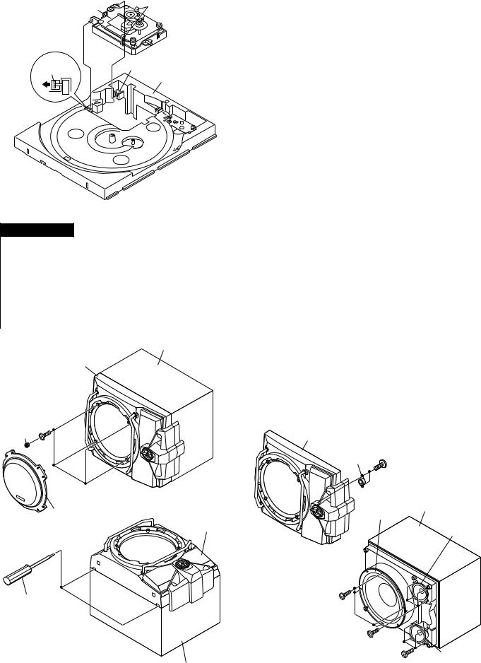
CD Mechanism |
1. |
Hook ......................... |
(Q1) x2 |
8-1 |
|||
|
|
2. |
Hook ......................... |
(Q2) x2 |
|
|||
Note 1: How to open the changer manually. (Fig. 6-3)
1.In this state, turn fully the lock lever in the arrow direction through the hole on the loading tray bottom.
2.After that, push forward the Loading tray.
CD-M8000W
Top Cabinet
Front (A1)x2 
 Panel ø3x12mm
Side Panel |
|
|
|
(Right) |
|
|
|
(B1)x2 |
|
|
(A1)x2 |
ø3x10mm |
|
|
ø3x12mm |
|
|
|
Side Panel |
|
|
|
(Left) |
(B1)x4 |
|
|
(B1)x2 |
ø3x10mm |
|
|
|
|
|
|
ø3x10mm |
|
Rear |
|
|
|
Panel |
|
|
|
Figure 6-1 |
|
|
|
CD Tray Cover |
(C2)x3 |
|
|
|
||
(C3)x1 |
2 |
1 |
|
Pull |
|
|
|
(C4)x2 |
|
|
|
CD Servo |
|
|
1 |
PWB |
|
|
2 |
|
|
|
|
|
|
|
CD Player |
Rear |
|
|
Unit |
|
|
|
|
Panel |
|
|
(C3)x1 |
|
|
|
|
(C1)x1 |
|
|
|
ø3x10mm |
|
|
Main PWB |
|
|
|
Lug Wire |
(D1)x8 |
|
|
(E1)x1 |
ø3x10mm |
|
|
|
|
|
ø3x10mm |
|
(D2)x1 |
|
|
|
|
|
(D1)x1 |
|
|
|
|
|
|
|
(E1)x1 |
ø3x10mm |
Amp. |
|
|
|
|
ø3x10mm |
|
|
PWB |
|
|
|
Figure 6-2
Lock Lever
CD Player Unit
(Bottom View)
Figure 6-3
Note 2:
1.After removing the connector for the optical pickup from the connector, wrap the conductive aluminium foil around the front end of the connector so as to protect the optical pickup from electrostatic damage.
Note 3:
1.Be careful not to break the claw of the CD mechanism.
2.When fining back the cam gear assembly, let it lock by front movement.
– 6 –

Tape |
(E2)x1 (E3)x1 Mic PWB |
|
Mechanism |
|
|
(E3)x1 |
(E3)x1 |
|
Power PWB |
|
Front |
|
|
|
|
|
Panel |
(G2)x1 |
|
|
Transformer |
|
|
PWB |
|
Main PWB |
|
|
|
|
|
(G2)x1 |
|
|
Main PWB |
|
|
(E3)x1 |
|
Figure 7-1 |
Amp. |
|
PWB |
(F1)x4 |
(F1)x1 |
|
ø3x6mm |
|
|
ø3x10mm |
|
|
|
(F2)x1 |
|
|
(F2)x3 |
Headphones |
|
|
PWB |
(F1)x1 |
|
(F4)x1 |
ø3x10mm |
|
|
Amp. |
|
|
PWB |
|
|
|
|
Front Panel |
(F3)x5 Push
(G1)x3 ø3x8mm 
Display PWB
(J2)x15
ø3x10mm
Tape
Mechanism
(K1)x5 |
ø3x10mm |
Figure 7-2
(J3)x1
Front Panel
(J1)x1
(H2)x1 
(H1)x2 |
ø3x10mm |
Mic
PWB
 Open
Open
Headphones
PWB
Lug Wire |
Cassette |
|
Holder |
(L1)x1 |
|
ø3x10mm |
Figure 7-3
CD-M8000W/CP-M8000
(M2)x1
Turntable
Loading
Tray
(M1)x2
CD Player Unit
Figure 7-4
(N1)x3 Loading Tray
3
2
1
(N1)x3
Figure 7-5
(P1)x2 |
ø3x10mm |
|
|
Loading |
(P3)x2 |
CD Servo |
Tray |
PWB |
|
(P2)x1
(P3)x2
Figure 7-6
– 7 –
CD-M8000W/CP-M8000
CD |
(Q2)x2 |
|
Mechanism |
||
|
(Q1)x1
(Q1)x1
Loading Tray
Figure 8-1
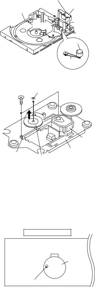
CP-M8000
STEP |
REMOVAL |
|
PROCEDURE |
|
FIGURE |
|
|
|
|
|
|
1 |
Front Panel/ |
1. Net Ass'y ................ |
(A1) x1 |
8-2 |
|
|
Supper Tweeter |
2. |
Catching Holder ..... |
(A2) x4 |
|
|
|
3. |
Screw ..................... |
(A3) x4 |
|
|
|
4. |
Screw ..................... |
(A4) x2 |
8-3 |
|
|
|
|
|
|
2 |
Woofer |
1. Screw ..................... |
(B1) x4 |
8-3 |
|
|
|
|
|
|
|
3 |
Tweeter |
1. Screw ..................... |
(C1) x4 |
8-3 |
|
|
|
|
|
|
|
4 |
Midrange |
1. Screw ..................... |
(D1) x4 |
8-3 |
|
|
|
|
|
|
|
Speaker Box Ass'y
Front Panel
(A3)x4
ø4x20mm
(A2)x4
(A1)x1
Front Panel
Driver should be pried away
from Speaker Box.
Front Panel
Super |
|
Tweeter |
(A4)x2 |
|
|
|
ø3x10mm |
Speaker Box Ass'y
Woofer
Tweeter
(B1)x4
ø4x20mm
(C1)x4
ø3x12mm
(D1)x4 |
Midrange |
ø3x12mm |
Speaker Box Ass'y
Figure 8-3
Figure 8-2
– 8 –

CD-M8000W/CP-M8000
REMOVING AND REINSTALLING THE MAIN PARTS
TAPE MECHANISM SECTION
Perform steps 1 to 7 and 10 of the disassembly method to remove the tape mechanism.
How to remove the record/playback and erase heads (TAPE 2) (See Fig. 9-1)
1.When you remove the screws (A1) x 2 pcs., the record/ playback head and three-dimensional head of the erase head can be removed.
How to remove the playback head (TAPE 1) (See Fig. 9-2)
1.When you remove the screws (B1) x 2 pcs., the playback head can be removed.
How to remove the pinch roller (TAPE 1/2) (See Fig. 9-3)
1. Carefully bend the pinch roller pawl in the direction of the arrow <A>, and remove the pinch roller (C1) x 1 pc., in the direction of the arrow <B>.
Note:
When installing the pinch roller, pay attention to the spring mounting position.
How to remove the belt (TAPE 2) (See Fig. 9-4)
1.Remove the main belt (D1) x 1 pc., from the motor side.
2.Remove the FF/REW belt (D2) x 1 pc.
TAPE 2
Clutch Ass'y
Record/Playback
Head
Erase Head
(A1) x 2 Ø2 x 6mm
Figure 9-1
TAPE 1
 Clutch Ass'y
Playback
Head
(B1) x 1  Ø2 x 9mm
(B1) x 1 Ø2 x 5mm
Figure 9-2
How to remove the belt (TAPE 1) (See Fig. 9-4)
1.Remove the main belt (E1) x 1 pc., from the motor side.
2.Remove the FF/REW belt (E2) x 1 pc.
How to remove the motor (See Fig. 9-5)
1. Remove the screws (F1) x 2 pcs., to remove the motor.
Tape
Motor
 Clutch Ass'y
(F1) x 2
Ø2.6 x 5mm
Figure 9-5
|
Pinch |
|
Roller |
Pinch Roller |
Pawl |
(C1) x 1 |
Pull <A> |
Pull |
|
|
<B> |
Figure 9-3
|
|
Tape |
|
FF/REW |
Tape |
Motor |
|
|
|
||
Roller |
Motor |
|
TAPE 1 |
TAPE 2 |
|
|
|
FF/REW |
|
TAPE 2 |
Main Belt |
Belt |
|
(E1) x 1 |
|
|
Main Belt |
||
(D2) x 1 |
|
|
|
|
(D1) x 1 |
|
|
|
|
|
|
Main Belt |
|
|
TAPE 1 |
|
|
|
|
(D1) x 1 |
|
|
FF/REW |
Flywheel |
|
|
|
|
|
Belt |
|
Ass'y |
|
|
(E2) x 1 |
Main Belt |
|
|
|
(E1) x 1 |
|
|
|
|
|
Flywheel |
FF/REW |
Figure 9-4 |
Ass'y |
Roller |
|
|
|
||
– 9 –
CD-M8000W/CP-M8000
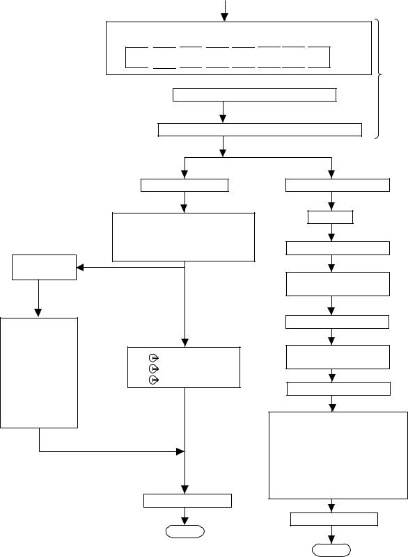
CD MECHANISM SECTION
Perform steps 1, 2, 3, 12, 13, 14 and 15 of the disassembly method to remove the CD mechanism.
How to remove the loading motor (See Fig. 10-1)
1.Bend the hooks (A1) x 5 pcs., to remove the loading motor.
2.Remove the drive belt (A2) x 1 pc.
|
Loading Motor |
Loading |
CD Loading |
Tray |
Motor PWB |
|
(A1) x 1 |
|
(A1) x 2 |
|
(A1) x 2 |
|
Loading |
|
Motor |
|
Pulley |
|
Drive Belt |
|
(A2) x 1 |
|
Figure 10-1 |
How to remove the pickup (See Fig. 10-2)
1.Remove the stop washer (B1) x 1 pc., to remove the gear (B2) x 1 pc.
2.Remove the screws (B3) x 2 pcs., to remove the shaft (B4).
3.Remove the pickup.
Note
After removing the connector for the optical pickup from the connector wrap the conductive aluminium foil around the front end of connector so as to protect the optical pickup from electrostatic damage.
(B3) x 2 |
Stop Washer |
|
|
ø2.6 x 6mm (B1) x 1 |
|
Pickup
Shaft |
CD Mechanism |
|
Gear |
||
(B4) x 1 |
||
(B2) x 1 |
||
|
||
|
Figure 10-2 |
ADJUSTMENT
MECHANISM SECTION
∙ Driving Force Check
Torque Meter |
Specified Value |
|
|
Play: TW-2111 |
Tape 1: Over 80 g |
|
Tape 2: Over 80 g |
|
|
∙ Torque Check
Torque Meter |
Specified Value |
|
|
|
|
|
Tape 1 |
Tape 2 |
|
|
|
Play: TW-2111 |
30 to 80 g.cm |
30 to 80 g.cm |
|
|
|
Fast forward: TW-2231 |
— |
70 to 180 g.cm |
|
|
|
Rewind: TW-2231 |
— |
70 to 180 g.cm |
|
|
|
∙ Tape Speed
|
Test Tape |
Adjusting |
Specified |
Instrument |
|
|
Point |
Value |
Connection |
|
|
|
|
|
Normal |
MTT-111 |
Variable |
3,000 ± 30 Hz |
Speaker |
speed |
|
Resistor in |
|
terminal |
|
|
motor. |
|
(Load |
|
|
|
|
resistance: |
|
|
|
|
6 ohms) |
|
|
|
|
|
TAPE MECHANISM
Tape
Motor
Variable Resistor in motor
Figure 10-3
– 10 –
TUNER SECTION
fL: Low-range frequency fH: High-range frequency
∙ AM IF/RF
Signal generator: 400 Hz, 30%, AM modulated
Test Stage |
Frequency |
Frequency |
Setting/ |
Instrument |
|
|
Display |
Adjusting |
Connection |
|
|
|
Parts |
|
|
|
|
|
|
AM IF |
450 kHz |
1,602 kHz |
T351 |
*1 |
|
|
|
|
|
AM Band |
— |
531 kHz |
(fL): T306 |
*2 |
Coverage |
|
|
1.1 ± 0.1 V |
|
|
|
|
|
|
AM Tracking |
990 kHz |
990 kHz |
(fL): T303 |
*1 |
|
|
|
|
|
*1. Input: Antenna |
Output: TP302 |
|
|
*2. Input: Antenna |
Output: TP301 |
|
|
SO301 |
CNP301 |
|
|
AM LOOP |
MAIN PWB |
||
FM ANTENNA |
ANTENNA |
|
|
TERMINAL |
|
|
|
|
IC301 |
T303 |
AM |
|
|
||
|
|
TRACKING fL |
|
|
|
|
|
TP301 |
T302 |
L312 |
|
C393 |
FM IF |
FM RF |
T306 |
|
|
||
T301 |
|
|
|
FM BAND |
|
|
AM BAND |
COVERAGE fL |
|
|
|
|
|
COVERAGE fL |
|
|
|
|
|
T351 |
|
|
|
AM IF |
|
TP302 |
|
|
|
||
|
|
|
R357 |
Figure 11-1 ADJUSTMENT POINTS
∙ FM RF
Signal generator: 1 kHz, 40 kHz dev., FM modulated
Test Stage |
Frequency |
Frequency |
Setting/ |
Instrument |
|
|
Display |
Adjusting |
Connection |
|
|
|
Point |
|
|
|
|
|
|
FM Band |
— |
87.50 MHz |
T301(fL): |
*1 |
Coverage |
|
|
3.4 V ± 50 mV |
|
|
|
|
|
|
FM RF |
98.00 MHz |
98.00 MHz |
L312 |
*2 |
|
(10-30 dB) |
|
|
|
|
|
|
|
|
*1. Input: Antenna |
Output: TP301 |
|
|||
*2. Input: Antenna |
Output: Speaker Terminal |
|
|||
∙ FM IF |
|
|
|
|
|
Signal generator: 10.7 MHz, FM modulated |
|
||||
|
|
|
|
|
|
Test Stage |
Frequency |
Frequency |
Setting/ |
Instrument |
|
|
|
|
Display |
Adjusting |
Connection |
|
|
|
|
Point |
|
|
|
|
|
|
|
IF |
10.7 MHz |
|
98 MHz |
T302 |
*1 |
|
|
|
|
(Turn the |
|
|
|
|
|
core of trans- |
|
|
|
|
|
former T302 |
|
|
|
|
|
fully counter- |
|
|
|
|
|
clock wise) |
|
|
|
|
|
|
|
*1. Input: Antenna |
Output: TP301 |
|
|||
CD-M8000W/CP-M8000
CD SECTION
•Adjustment
Since this CD system incorporates the following automatic adjustment functions, readjustment is not needed when replacing the pickup. Therefore, different PWBs and pickups can be combined freely.
Each time a disc is changed, these adjustments are performed automatically. Therefore, playback of each disc can be performed under optimum conditions.
Items adjusted automatically
(1)Offset adjustment (The offset voltage between the head amplifier output and the VREF reference voltage is compensated inside the IC.)
*Focus offset adjustment
*Tracking offset adjustment
(2)Tracking balance adjustment (waveform drawing Fig. 11-2 EFBL)
(3)Gain adjustment (The gain is compensated inside the IC so that the loop gain at the gain crossover frequency will be 0 dB.)
*Focus gain adjustment
*Tracking gain adjustment
CD ERROR CODE DESCRIPTION
Error |
Explanation |
|
|
|
|
01 |
When Pickup set inner position, inner switch |
|
cannot detect 'ON' level for 10 secs. |
||
|
||
|
When tray moves to Open/Close, Open/Close switch |
|
10* |
cannot detect 'ON' level for 7 secs. |
|
When disc table rotate to target position. |
||
|
||
|
Clamp switch cannot detect 'ON' level for 7 secs. |
|
|
When disc table set to Disc1 position for 1 st time, |
|
11* |
"CLAMP SW", "DISC NO SW" and "OPEN/CLOSE" |
|
|
cannot detect 'ON' level for 14 secs. |
|
|
|
|
31 |
When it changes to CD function, DSP cannot read |
|
initial data. |
||
|
||
|
|
* 'CHECKING'
If Error is detected, 'CHECKING' will be display instead of 'ERCD**' display. 'ER-CD**' display will only be display when error had been detected for the 5 th times.
|
Stopped |
|
T |
|
|
|
|
|
1999/04/05 |
20:26:47 |
|
|
|
|
|
|
|
|
|||
|
CH1=500 mV |
CH2=200 mV |
CH3=1 V |
|
|
500 ms/div |
||||
|
DC |
10:1 |
|
DC |
10:1 |
DC 10:1 |
|
|
(500 ms/div) |
|
|
|
|
|
|
|
|
|
|
NORM:20 kS/s |
|
T |
FDO |
|
|
|
|
|
|
|
|
|
|
|
|
|
|
|
|
|
|
|
|
1 |
|
|
|
|
|
|
|
|
|
|
3 |
TE |
|
|
|
|
|
|
|
|
|
|
|
|
|
|
|
|
|
|
|
|
|
EFBL |
|
|
|
|
|
|
|
|
|
2 |
|
|
|
|
|
|
|
|
|
|
|
|
|
|
|
|
|
|
|
|
CH2 |
|
|
|
|
|
|
|
|
|
|
v/DIV |
|
|
|
|
|
|
|
|
|
|
200 mV |
|
=Filter= |
|
|
=Offset= |
=Record Length= |
|
=Trigger= |
|||
Smoothing : ON |
CH1 : |
0.000 V |
Main : |
100 K |
Mode : SINGLE |
|||||
BW |
: FULL |
|
CH2 : |
0.000 V |
Zoom : |
2 k |
Type |
: EDGE CH1 |
||
|
|
|
CH3 : |
0.00 V |
|
|
Delay : |
0.0 ns |
||
|
|
|
CH4 : |
0.00 V |
|
|
Hold off : |
0.2 s |
||
|
|
|
|
|
Figure 11-2 |
|
|
|
||
– 11 –
CD-M8000W/CP-M8000
TEST MODE
• Setting the test mode
Any one of test mode can be set by pressing several keys as follows. <X-BASS> + <CD> + <POWER> TEST:CD operation test
Function:-CD test mode. -Enter test mode.
C
 D
D 


 T
T 
 E
E 
 S
S 
 T
T 

IL isn't done
OPEN/CLOSE operation is using manual.
<< >>, <<
 >> buttons make pick's slide possible.
<<PLAY>> key input.
Do TOC IL. Do normal play When these following key is input into PLAY key, track number can be appoint directly
<<MEMORY>> key input
|
Adjustment result |
|
|
|
automatically will |
|
|
|
display as below |
|
|
|
for each 2 sec : |
<< 1>> key: Track 4 |
|
|
a) "FOFF_XX" |
<< 2>> key: Track 9 |
|
|
b) "TOFF_XX" |
<< 3>> key: Track 15 |
|
|
c) "TBAL_XX" |
|
|
|
d) "TGAN_XX" |
|
|
|
f) "FGAN_XX" |
|
|
|
g) "RFLS_XX" |
|
|
explanation: |
|
|
|
a) |
Focus off set |
="FOFF_XX" |
|
b) |
Tracking off set |
="TOFF_XX" |
|
c) |
Tracking balance |
="TBAL_XX" |
<<STOP>> key input. |
d) |
Tracking Gain |
="TGAN_XX" |
|
f) |
Focus Gain |
="FGAN_XX" |
|
g) |
RF level shift |
="RFLS_XX" |
STOP |
VOL — Last memory
BAL — CENTER
P.GEQ — FLAT
X-BASS — OFF
To cancel : Power OFF
<<MEMORY>> key input.
Laser ON.
<<MEMORY>> key input.
Tracking OFF play at that specific point.
<<MEMORY>> key input.
Tracking ON play from that specific point.
<<MEMORY>> key input.
Adjustment result automatically will display as below for each 2 sec :
a)"FOFF_XX"
b)"TOFF_XX"
c)"TBAL_XX"
d)"TGAN_XX"
f)"FGAN_XX"
g)"RFLS_XX"
<<STOP>> key input.
STOP
Sliding the PICKUP with << >>, <<
 >> button
must only be in STOP mode.
– 12 –
|
|
|
CD-M8000W/CP-M8000 |
|
Standard Specification of Stereo System Error Message Display Contents |
||||
|
|
|
|
|
|
Error Contents |
DISPLAY |
Notes |
|
|
|
|
|
|
TAPE |
Mechanism Error. |
'ER-TA**' |
00: Tape Mechanism Error. |
|
|
|
|
01: Initial Error. |
|
|
|
|
02: |
|
|
|
|
03: |
|
|
|
|
|
|
CD |
Pickup Mechanism Error. |
'ER-CD**' |
01: PU-IN SW Detection NG. |
|
|
|
|
02: |
|
|
|
|
03: |
|
|
|
|
04: |
|
|
|
|
|
|
|
CD Changer Mechanism Error. |
'ER-CD**' |
10: Changer Error. |
|
|
|
(*) |
11: Initial Error. |
|
|
|
|
12: |
|
|
|
|
13: |
|
|
|
|
|
|
|
CD DSP Communication Error |
'ER-CD**' |
31: DSP COMMUNICATION ERROR |
|
|
|
|
|
|
|
Focus Not Match. |
'NO DISC' |
|
|
|
|
|
|
|
|
IL Time Over. |
'NOT READ' |
|
|
|
|
|
|
|
TUN |
PLL Unlock. |
'ER-TU**' |
00: TUN Error. |
|
|
|
|
01: PLL Unlock. |
|
|
|
|
02: |
|
|
|
|
03: |
|
|
|
|
|
|
(*) CHECKING:
If CD changer mechanism error is detected, 'CHECKING' will be display instead of 'ER-CD**' display 'ER-CD**' will only be display when CD changer mechanism error had been detected for the 5 th times.
Speaker abnormal detection and +B PROTECTION display
In case speaker abnormal detection or +B PROTECTION had occured, it can be check by pressing 'POWER', 'VIDEO' and 'X- BASS' key twice. Display will show "S** B**". S is referring to speaker abnormal detection and B is referring to +B PROTECTION. ** is in hex valve.
+B PROTECTION is condition when irregular process occur on power supply line.
– 13 –
CD-M8000W/CP-M8000
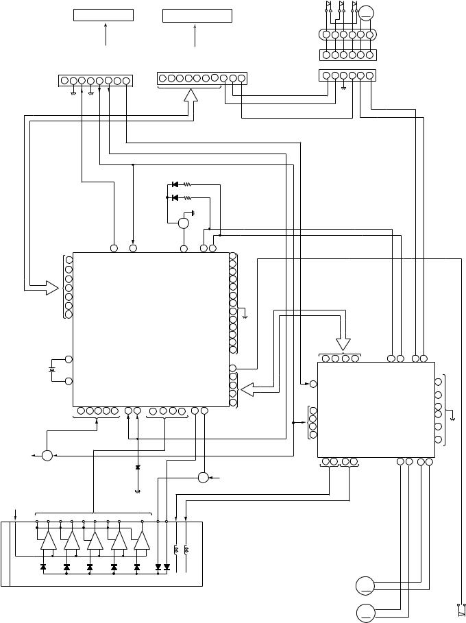
NOTES ON SCHEMATIC DIAGRAM
∙Resistor:
To differentiate the units of resistors, such symbol as K and M are used: the symbol K means 1000 ohm and the symbol M means 1000 kohm and the resistor without any symbol is ohm-type resistor. Besides, the one with “Fusible” is a fuse type.
∙Capacitor:
To indicate the unit of capacitor, a symbol P is used: this symbol P means pico-farad and the unit of the capacitor without such a symbol is microfarad. As to electrolytic capacitor, the expression “capacitance/withstand voltage” is used.
(CH), (TH), (RH), (UJ): Temperature compensation (ML): Mylar type
(P.P.): Polypropylene type
∙Schematic diagram and Wiring Side of P.W.Board for this model are subject to change for improvement without prior notice.
∙The indicated voltage in each section is the one measured by Digital Multimeter between such a section and the chassis with no signal given.
1.In the tuner section, indicates AM indicates FM stereo
2.In the main section, a tape is being played back.
3.In the deck section, a tape is being played back. ( ) indicates the record state.
4.In the power section, a tape is being played back.
5.In the CD section, the CD is stopped.
∙Parts marked with “ ” (
” ( 


 ) are important for maintaining the safety of the set. Be sure to replace these parts with specified ones for maintaining the safety and performance of the set.
REF. NO |
DESCRIPTION |
POSITION |
|
|
|
SW1 |
OPEN/CLOSE |
ON—OFF |
|
|
|
SW2 |
CLAMP |
ON—OFF |
|
|
|
SW3 |
DISC NUMBER |
ON—OFF |
|
|
|
SW4 |
PICKUP IN |
ON—OFF |
|
|
|
SW601 |
SPAN SELECTOR |
50 kHz/9 kHz |
|
|
|
SW701 |
ON/STAND-BY |
ON—OFF |
SW702 |
FAST REWIND/PRESET DOWN |
ON—OFF |
|
|
|
SW703 |
FAST FORWARD/PRESET UP |
ON—OFF |
|
|
|
SW704 |
STOP |
ON—OFF |
|
|
|
SW705 |
PLAY |
ON—OFF |
|
|
|
SW706 |
REVERSE PLAY |
ON—OFF |
|
|
|
SW707 |
REVERSE MODE |
ON—OFF |
SW711 |
CD |
ON—OFF |
|
|
|
SW712 |
TUNER (BAND) |
ON—OFF |
|
|
|
REF. NO |
DESCRIPTION |
POSITION |
|
|
|
SW713 |
TAPE |
ON—OFF |
|
|
|
SW714 |
VIDEO/AUX |
ON—OFF |
|
|
|
SW715 |
TIMER/SLEEP |
ON—OFF |
|
|
|
SW716 |
TUNING/TIME UP |
ON—OFF |
SW717 |
REC PAUSE |
ON—OFF |
|
|
|
SW718 |
MEMORY/SET |
ON—OFF |
|
|
|
SW719 |
TUNING/TIME DOWN |
ON—OFF |
|
|
|
SW720 |
CLOCK |
ON—OFF |
|
|
|
SW723 |
DISC SKIP |
ON—OFF |
|
|
|
SW724 |
OPEN/CLOSE |
ON—OFF |
SW725 |
EQUALIZER |
ON—OFF |
|
|
|
SW726 |
MONSTER BASS |
ON—OFF |
|
|
|
SW801 |
VOLTAGE SELECTOR |
230-240 V |
|
|
|
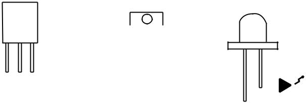
TYPES OF TRANSISTOR AND LED
FRONT |
|
|
|
|
|
|
|
|
|
FRONT |
|||||
VIEW |
|
|
|
|
|
|
|
|
|
||||||
|
|
|
FRONT |
|
VIEW |
||||||||||
|
|
|
|
VIEW |
|
|
|
|
|
||||||
E |
C B |
|
|
|
|
|
|
|
|
|
|
|
|
|
|
|
|
|
|
|
|
|
|
|
|
|
|
|
|||
(S) (G) (D) |
|
|
|
|
|
|
|
|
|
|
|
|
|
||
|
|
|
|
|
|
|
|
|
|
|
|
|
|||
(1) |
(2) (3) |
|
|
|
|
|
|
|
|
|
|
|
|
|
|
|
B C E |
|
|
|
|
|
|||||||||
KTA1266 GR |
KTC3203 Y |
|
|
|
|
|
|
||||||||
(1) |
(2) (3) |
|
|
|
|
|
|||||||||
KTA1273 Y |
KRC102 M |
SRL342VCJ |
|||||||||||||
|
KTC2026 |
||||||||||||||
KTA1274 Y |
KRC104 M |
|
4204UYT7 |
||||||||||||
|
|
|
|
|
|
|
|
||||||||
KTC3194 Y |
KRA107 M |
|
|
|
|
|
|
|
|
A503BC2E |
|||||
KTC3199 GR |
2SA1015 GR |
|
|
|
|
|
|
|
|
|
|
|
|
|
|
|
2SC1845 F |
|
|
|
|
|
|
|
|
|
|
|
|
|
|
– 14 –
|
|
|
TO MAIN SECTION |
|
TO DISPLAY SECTION |
|
|
|
|||||||||||
|
R-CH |
AGND |
L-CH |
DGND |
+5V (+B7) |
+5V (+B8) |
DGND (DRIVER) |
+6.5V (+B4) |
WRQ |
DRF |
CE |
DO |
DI |
CL |
CD RES |
CLAMP SW |
O/C |
DISC NO |
|
CNP7 |
1 |
2 |
3 |
4 |
5 |
6 |
7 |
8 |
1 |
2 |
3 |
4 |
5 |
6 |
7 |
8 |
9 |
10 |
CNP8 |
|
|
|
|
|
|
|
|
|
|
|
|||||||||
CD-M8000W/CP-M8000
|
SW2 |
SW3 |
|
|
DISC |
||
SW1 |
CLAMP |
||
NUMBER |
|||
OPEN/ |
|
M3 |
|
CLOSE |
|
T/T UP DOWN |
|
|
|
M LOADINGMOTOR |
+–
1 |
2 |
3 |
4 |
5 |
6 |
BI4 |
1 |
2 |
3 |
4 |
5 |
6 |
CNS4 |
1 |
2 |
3 |
4 |
5 |
6 |
CNP4 |
|
|
|
|
|
|
|
|
|
|
|
|
Q3 |
|
|
|
|
|
|
|
|
|
|
|
|
|
|
|
|
|
|
|
|
42 |
68 |
|
|
|
25 |
|
70 |
71 |
|
|
|
|
|
|
|
|
|
|
|
|
|
|
61 |
CE |
|
|
LCHO |
VDD5 |
|
|
|
|
CONT4 |
|
CONT3 |
CONT2 |
75 |
|
|
|
|
|
|
|
|
|
|
|
|
|
|
|
|
|
|
|
69 |
|
|
|
|
|
|
|
|
|
|
|||||||
|
|
|
|
|
|
|
|
|
|
|
|
|
|
|
|
|
|
|
|
|
||||||
|
|
62 |
CLK |
|
|
|
|
|
|
|
57 |
|
|
|
|
|
|
|
|
|
|
|||||
|
|
|
|
|
|
|
|
|
|
|
|
|
|
|
|
|
|
|
|
|
|
|
|
|
|
|
|
|
63 |
DI |
|
|
|
|
|
|
|
|
|
|
|
|
56 |
|
|
|
|
|
|
|
|
|
|
|
|
64 |
DO |
|
|
|
|
|
|
|
|
|
|
|
|
55 |
|
|
|
|
|
|
|
|
|
|
|
|
65 WRQ |
|
|
|
|
|
|
|
|
|
|
|
|
51 |
|
|
|
|
|
|
|
|
|
|
|
|
|
|
|
|
|
|
|
|
|
|
|
|
|
50 |
|
|
|
|
|
|
|
|
|
|
||
|
|
66 |
RES |
|
|
|
|
|
|
|
|
|
|
|
|
|
|
|
|
|
|
|
|
|
|
|
|
|
|
|
|
|
|
|
|
|
|
|
|
|
44 |
|
|
|
|
|
|
|
|
|
|
||
|
|
67 |
DRF |
|
|
|
|
|
IC1 |
|
|
|
|
|
|
|
|
|
|
|
|
|
|
|
|
|
|
|
|
|
|
|
|
|
|
|
|
|
|
43 |
|
|
|
|
|
|
|
|
|
|
|||
|
|
|
|
|
|
|
|
|
|
|
|
|
|
|
|
|
|
|
|
|
|
|
|
|
||
|
|
|
|
|
|
|
LC78645NE |
|
|
|
40 |
|
|
|
|
|
|
|
|
|
|
|||||
|
|
|
|
|
|
|
|
|
|
37 |
|
|
|
|
|
|
|
|
|
|
||||||
|
|
|
|
|
|
|
CD SERVO |
|
|
|
|
|
|
|
|
|
|
|
|
|
|
|||||
|
|
|
|
|
|
|
|
|
|
|
28 |
|
|
|
|
|
|
|
|
|
|
|||||
|
|
|
|
|
|
|
|
|
|
|
|
|
|
|
|
19 |
|
|
|
|
|
|
|
|
|
|
|
MHz |
48 |
XOUT |
|
|
|
|
|
|
|
|
|
|
|
|
|
1 |
2 |
17 |
25 |
41 42 |
|
38 39 |
|
|
|
XL1 |
|
|
|
|
|
|
|
|
|
|
|
|
|
CONT5 26 |
|
|
|
|
|
|
|
|
|
|
||
33.8688 |
|
|
|
|
|
|
|
|
|
|
|
|
|
|
|
|
|
|
|
|
|
|
|
|||
49 |
XIN |
|
|
|
|
|
|
|
|
|
|
|
SLDO 23 |
|
|
|
|
|
|
|
|
|
35 |
|||
ADAVDD |
|
|
|
|
|
|
|
|
|
|
SPDO 22 |
40 |
VCC4 |
|
|
|
|
|
|
|
||||||
|
|
|
RFVDD |
|
|
|
|
|
|
|
|
|
|
|
|
|
IC2 |
|
|
|
~ |
|||||
|
|
|
VDD XVDD |
VVDD |
LVDD |
RVDD |
|
|
|
|
|
|
FDO 21 |
|
|
|
|
|
|
|
|
|||||
|
|
|
FIN1 |
FIN2 |
TIN1 |
TIN2 |
LDS |
LDD |
|
|
|
|
|
|
|
|
29 |
|||||||||
|
|
|
|
|
|
|
|
|
|
|
|
|
||||||||||||||
|
|
|
TDO |
20 |
|
|
|
|
|
|
|
|
22 |
|||||||||||||
|
|
|
|
|
|
|
41 |
46 |
|
|
|
|
79 |
80 |
|
|
|
|
|
|
M63001FP |
|
|
|
||
|
|
|
5 |
18 38 47 77 |
7 |
8 |
9 |
10 |
|
+5V |
18 |
VCC1 |
FOCUS/TRACKING/ |
21 |
||||||||||||
|
|
|
|
|
|
|
|
|
|
|
|
|
|
|
|
|
24 |
VCC2 |
|
|
SPIN/SLED |
|
|
|
||
|
|
+3.3V |
|
|
|
|
|
|
|
|
|
|
|
|
|
|
23 |
|
|
|
|
|
14 |
|||
|
|
|
|
|
|
|
|
|
|
|
|
|
|
|
|
|
28 |
VCC3 |
|
|
|
DRIVER |
|
|
|
~ |
|
|
|
|
|
|
|
|
|
|
|
|
|
|
|
|
|
|
|
|
|
|
|
8 |
|||
|
|
|
|
|
|
|
|
|
|
|
|
|
|
|
|
|
|
|
|
|
|
|
|
|
|
|
+3.3V |
Q2 |
|
|
|
|
|
|
|
|
|
|
|
|
|
|
|
|
4 |
5 |
6 |
7 |
|
|
|
|
|
CONSTANT |
|
|
|
|
ZD1 |
|
|
|
|
|
|
|
LASER |
|
|
15 |
16 |
26 |
27 |
|
||||||
|
|
|
|
|
|
|
|
|
|
|
|
|
|
|
|
|
|
|
|
|
|
|||||
VOLTAGE |
|
|
|
|
|
3.3V |
|
|
|
|
|
|
|
DRIVER |
|
|
|
|
|
|
|
|
|
|
|
|
|
|
|
|
|
|
|
|
|
|
|
|
|
|
Q1 |
+3.3V |
|
|
|
|
|
|
|
|
|
|
|
+5V(+B7) |
|
|
|
|
|
|
|
|
|
|
|
|
|
|
|
|
|
|
|
|
|
|
|
|
|
|
PICKUP UNIT |
|
|
|
|
|
|
|
|
|
|
|
FOCUS COIL |
TRACKING COIL |
|
|
|
|
|
|
|
|
|
|
|
|
|
|
|
|
|
|
|
|
|
|
|
|
|
|
|
|
|
|
|
|
|
M1 |
|
+ |
|
|
|
|
|
|
|
|
|
|
|
|
|
|
|
|
|
|
|
|
|
|
|
SPINDLE |
M |
|
|
|
|
||
|
|
|
|
|
|
|
|
|
|
|
|
|
|
|
|
|
|
|
MOTOR |
|
|
|
|
|
||
|
|
|
|
|
|
|
|
|
|
|
|
|
|
|
|
|
|
|
|
|
|
– |
|
|
|
|
|
|
|
|
|
|
|
|
|
|
|
|
|
|
|
|
|
|
|
|
|
|
– |
|
|
|
SW4 |
|
|
|
|
|
|
|
|
|
|
|
|
|
|
|
|
|
|
|
|
M2 |
|
M |
|
|
|
|
|
|
|
|
|
|
|
|
|
|
|
|
|
|
|
|
|
|
|
|
|
|
|
|
PICKUP IN |
||
|
|
|
|
|
|
|
|
|
|
|
|
|
|
|
|
|
|
|
|
SLED |
|
|
|
|||
|
|
|
|
|
|
|
|
|
|
|
|
|
|
|
|
|
|
|
|
MOTOR |
+ |
|
|
|
|
|
Figure 15 BLOCK DIAGRAM (1/3)
– 15 –
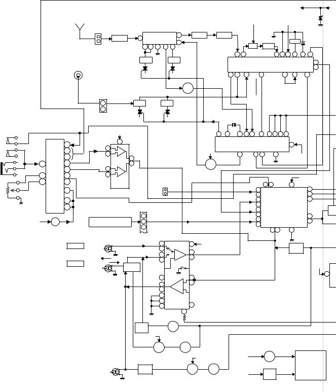
CD-M8000W/CP-M8000
|
|
IC301 |
|
|
|
|
|
|
|
|
+B6 |
|
|
+B |
|||
FM |
|
|
|
|
|
|
|
|
|
|
|
ZD351 |
|||||
ANTENNA SO301 |
TA7358AP |
|
|
|
|
+B6 |
|
+B6 |
|
5.1V |
|||||||
FM ANTENNA |
FM FRONT END |
FM IF |
|
|
|
|
|
|
|
10.7 MHz |
|
||||||
TERMINAL |
|
|
|
|
|
|
|
|
|||||||||
BF301 |
1 |
|
|
|
6 |
T302 |
CF303 |
|
|
|
|
|
|
|
|
X351 |
|
|
|
|
9 |
|
|
|
|
|
|
|
|
CF351 |
|
||||
B.P.F |
|
|
|
|
|
|
|
|
T351 |
|
|
|
|
456 kHz |
|||
3 |
4 |
5 |
7 |
|
|
|
|
CF352 |
|
|
|
|
|||||
|
8 |
|
|
1 |
2 |
5 |
9 |
8 |
17 13 |
||||||||
|
|
|
|
FM |
OSC |
|
|
|
4 |
||||||||
|
|
|
|
|
|
|
|
|
AM IF |
AM IF |
FM/AMGND |
OUT FM+B |
MPXIN |
|
FM/AM MO/ST |
|
|
ANTENNA |
|
|
|
|
OSC |
|
|
|
AMMIX |
|
VCO |
|
|||||
FM RF L312 |
|
|
T301 |
|
|
|
|
|
|
|
|
FM DET |
|
|
L 14 |
||
AM LOOP |
|
|
|
|
FM |
|
|
|
|
|
|
|
|
|
|
|
R 15 |
|
|
|
|
|
|
|
|
|
|
|
|
|
|
|
|
||
CNP301 |
AM TRACKING |
|
24 |
23 |
21 |
7 |
|
18 |
16 |
|
12 |
|
|||||
|
OSCAMOUT |
OSCAM IN |
RFAMIN |
STEREO |
LA1832S |
|
|
|
|||||||||
|
|
|
|
|
OSC BUFF |
|
|
|
|
|
|
|
|
|
|
|
|
|
|
|
|
|
Q302 |
|
|
|
|
|
IC302 |
|
|
|
|
||
1 |
|
|
|
|
AM BAND |
|
|
|
|
|
FM IF DET./ |
|
|
|
|||
T303 |
|
|
T306 COVERAGE |
|
|
|
|
FM MPX./ |
|
|
|
||||||
2 |
|
|
|
|
|
|
|
|
|
|
AM IF |
|
|
|
|
||
|
|
|
|
|
|
|
|
|
|
|
|
|
|
|
|||
|
|
ICK1 |
|
|
|
|
|
|
|
|
|
|
VT |
X352 |
|
|
|
|
|
|
|
||
|
|
|
|
|
|
|
|
|
|
|
|
4.5 MHZ |
|
|
|
|
|
|
|
||||
|
M65856SP |
|
|
|
|
|
|
|
|
|
|
|
|
|
|
|
CE DI CLK |
|
DO |
|
|||
JK1 |
MIC AMP. |
|
|
+B5 |
|
|
|
|
IC303 |
|
|
|
|
|
|
|
|
||||||
MIC |
|
|
|
|
|
|
|
|
|
|
20 |
1 |
22 15 16 |
11 |
3 |
4 |
5 |
6 |
|
||||
|
|
|
|
|
|
5 |
|
|
|
|
LC72131 |
|
|
|
OSC |
FM/AM |
MO/ST |
|
|
|
|
|
|
|
|
|
|
|
|
|
|
|
PLL(TUNER) |
|
|
|
|
|
|
|
|
|
|||||
|
|
LATCH 40 |
|
|
8 |
|
|
|
|
|
|
|
|
|
|
|
|
|
|
|
17 |
|
|
|
|
|
|
|
|
|
|
|
|
|
|
|
|
|
|
|
|
|
|
|
|||
|
|
CLOCK 41 |
|
|
6 |
|
|
|
|
|
|
|
+B5 |
|
7 |
9 |
10 |
21 |
|
|
|
||
|
MIC IN |
DATA 42 |
|
|
1 L |
|
|
|
|
|
|
|
|
|
+B5 |
|
|||||||
|
|
|
|
|
|
|
|
|
|
|
|
|
|
|
|
|
|
|
|||||
|
|
L OUT 36 |
|
|
|
|
|
|
|
FM+B |
Q360 FM |
|
|
|
|
|
|
|
|
||||
|
9 |
|
|
2 |
7 R |
|
|
|
|
|
|
|
|
|
|
|
|
||||||
|
|
R OUT 35 |
|
|
|
|
|
|
|
SWITCHING |
|
|
|
|
|
|
|
|
|
||||
|
12 |
L IN |
31 |
IC903 |
3 |
|
|
|
|
|
|
|
|
|
|
|
|
|
|
||||
|
|
|
|
JK690 |
|
|
|
|
|
|
|
|
|
|
+B5 |
|
|||||||
|
13 |
R IN 32 |
|
|
|
|
|
|
|
|
|
|
|
|
|
|
|
||||||
|
KIA4558P |
|
|
VIDEO/AUX |
|
|
|
|
|
|
|
8 17 |
|
|
23 |
|
|||||||
|
|
|
|
|
|
|
|
|
|
|
|
|
|
|
|
||||||||
VRK1 |
|
VCC 23 |
OPE AMP. |
|
|
|
L |
AUX |
|
|
|
|
|
L 9 |
|
|
|
DI 1 |
|
||||
MIC |
|
|
|
|
|
|
|
|
|
R |
|
|
|
|
|
|
R 16 |
|
|
|
CE 2 |
|
|
VOLUME |
|
MCLKCONT |
2 |
|
|
|
|
|
|
|
|
|
|
|
|
TAPE |
L 10 |
|
IC601 CLK 24 |
–20dB |
|||
|
|
VACL |
3 |
|
|
|
|
|
|
|
|
|
|
|
|
|
R 15 |
LC75341 |
ATT Q6 |
||||
|
|
|
|
|
CNS11 |
|
|
|
|
|
|
|
TUNER |
L 11 |
|||||||||
|
|
|
|
|
|
|
|
1 |
|
|
|
|
|
|
|
R 14 AUDIO PROCESSOR 21 R |
Q6 |
||||||
|
|
|
|
|
|
|
|
|
|
|
|
|
|
|
|
||||||||
|
+B5 |
QK1 |
|
|
|
CNP7 |
|
|
2 |
|
|
|
|
|
|
CD |
L 12 |
|
|
|
4 L |
|
|
|
|
|
|
|
FROM CD SECTION |
|
3 |
|
|
|
|
|
|
|
R 13 |
7 18 |
3 |
|
|||||
|
|
|
|
|
|
|
|
|
|
|
|
|
|
|
|
|
|
|
|||||
|
|
|
|
|
|
|
|
|
|
|
|
|
|
|
|
|
|
|
|
||||
|
|
|
|
|
|
|
|
|
|
|
|
|
|
|
|
|
|
|
L |
R |
|
|
|
|
|
|
TAPE 1 |
L-CH |
|
|
|
L(T1) 1 |
|
13 |
+B5 |
|
|
|
|
|
|
|
Q121 |
REC |
|||
|
|
|
|
|
|
R(T1) 24 |
|
P.B |
|
|
|
|
|
|
|
|
|
||||||
|
|
|
P.B. HEAD R-CH |
|
|
|
|
L PB |
|
|
|
|
|
|
|
Q122 |
|
||||||
|
|
|
|
|
|
L(T2) 2 |
|
4 |
|
|
|
|
|
|
|
|
|||||||
|
|
|
|
|
|
REC. |
|
|
|
21 |
R |
|
|
|
|
|
|
|
|
MUTING |
|
||
|
|
|
|
|
|
|
|
R(T2) 23 |
|
|
|
|
|
|
|
|
|
|
|||||
|
|
|
|
|
|
SWITCHING |
|
|
|
|
|
|
|
|
|
|
|
||||||
|
|
|
TAPE 2 |
P.B. |
|
|
|
|
|
|
|
|
|
|
|
|
|
||||||
|
|
|
Q103~ |
|
|
|
|
|
|
|
|
|
|
|
|
|
|
|
|
||||
|
|
|
L-CH |
|
|
|
|
|
|
|
|
|
|
|
|
|
|
|
+B5 |
||||
|
|
|
REC./P.B. |
R-CH |
|
Q106 |
|
|
|
|
|
|
|
|
|
|
|
|
|
|
|||
|
|
|
|
|
|
|
|
|
|
|
|
|
|
|
|
|
|
|
8 |
||||
|
|
|
HEAD |
|
|
|
|
POP REDUCE 6 T1/T2 |
H/N 7 |
L REC |
|
|
|
|
|
|
|
|
|||||
|
|
|
|
|
AC BIAS |
|
|
|
|
|
|
|
|
|
|
|
|||||||
|
|
|
|
|
|
|
|
|
L REC 9 REC |
18 |
R |
IC101 |
|
|
|
|
|
|
|
|
|||
|
|
|
|
|
|
|
|
|
R REC 16 |
|
|
|
|
|
|
|
|
|
|
IC |
|||
|
|
|
|
|
|
|
|
|
|
11 |
|
|
|
AN7345K |
|
|
|
|
|
|
|||
|
|
|
|
|
|
|
|
|
|
12 NOR/ |
T1/T2 10 |
ALC |
PLAYBACK AND RECORD |
KIA4 |
|||||||||
|
|
|
|
|
|
|
|
|
|
15 HIGH |
/PLAYBACK AMP. |
|
|
|
OPE |
||||||||
|
|
|
|
|
|
|
|
|
|
|
|
19 |
|
|
|
|
|||||||
|
|
|
|
|
|
|
|
|
|
|
|
|
|
|
|
|
|
|
|
|
|
|
|
|
|
|
|
|
|
|
|
|
SWITCHING |
|
|
|
|
|
|
|
|
|
|
|
|
||
|
|
|
|
|
|
|
Q107 |
|
Q111 |
|
|
|
|
|
|
|
|
|
|
|
|
||
|
|
|
|
|
|
|
Q108 |
SWITCHING |
|
|
|
|
|
|
|
|
|
|
|
||||
|
|
|
|
|
|
|
|
|
+B5 |
|
|
|
|
|
|
|
|
|
|
|
|||
|
|
|
|
|
|
|
|
|
|
|
|
|
|
|
|
|
|
|
|
|
|
|
|
|
|
|
|
|
|
|
|
|
Q109 |
|
Q110 |
|
|
|
|
|
MOTOR |
|
|
|
|||
|
|
|
|
|
|
|
|
|
|
|
|
|
|
|
DRIVER |
|
|
|
|||||
|
|
|
|
|
|
|
|
|
|
SWITCHING |
+B5 |
|
|
+B3 |
|
|
Q706 |
|
|
TAPE |
|
||
|
|
|
|
|
|
|
|
|
|
|
|
|
|
|
|
|
|
|
|
|
|
|
|
|
|
|
|
|
ERASE |
|
Q128 |
|
|
Q124 |
Q126 |
|
|
|
|
|
|
|
MECHANISM |
||||
|
|
|
|
|
|
|
|
|
|
|
|
Q707 |
|
|
ASS'Y |
||||||||
|
|
|
|
|
|
L104 |
|
|
|
|
|
|
|
|
|||||||||
|
|
|
|
|
HEAD |
|
|
|
|
|
|
|
+B3 |
|
|
|
|
|
|
||||
|
|
|
|
|
|
BIAS |
|
SWITCHING |
BIAS |
|
|
|
Q708 |
|
|
|
|
||||||
|
|
|
|
|
|
|
|
|
|
|
|
|
|
|
|
|
|||||||
|
|
|
|
|
|
|
|
OSC |
|
|
|
|
|
|
|
|
SOLENOID |
|
|
||||
|
|
|
|
|
|
|
|
|
|
|
|
|
|
|
|
|
|
DRIVER |
|
|
|
||
Figure 16 BLOCK DIAGRAM (2/3)
– 16 –
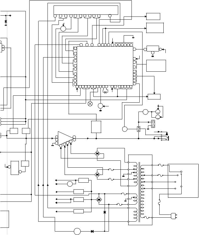
|
|
|
|
|
|
|
|
|
|
|
|
|
|
|
|
|
|
|
|
|
CD-M8000W/CP-M8000 |
||||
|
|
|
|
|
|
|
|
|
|
|
|
FL701 |
|
|
|
|
|
|
|
|
|
|
|
||
|
|
|
|
|
|
|
|
|
|
|
FL DISPLAY |
|
|
|
|
|
|
TO CD |
|
|
|
||||
|
+B5 |
|
|
|
|
|
1 |
5 ~ 12 |
13 |
14 ~ 19 |
27 ~ 32 33 ~41 |
45 |
|
|
|
|
|
|
|
||||||
|
|
|
|
|
|
|
|
|
|
|
|
|
|
|
|
|
|
|
|
|
|
SECTION |
|
|
|
351 |
|
|
|
|
|
|
|
|
+B9 |
|
|
|
|
|
|
|
|
|
|
|
|
|
|
|
|
1V |
|
|
|
|
|
|
|
|
|
|
|
|
|
|
|
|
|
|
|
TAPE |
|
|
|
||
|
|
|
|
|
|
|
|
|
|
|
|
|
|
|
|
|
|
|
|
|
|
|
|
|
|
|
|
|
|
|
|
|
|
Q705 |
|
|
|
|
|
|
|
|
|
|
|
MECHANISM |
|
|
|||
|
|
|
|
|
|
|
|
|
|
|
|
|
|
|
|
|
|
|
|
ASS'Y |
|
|
|
||
|
|
|
|
|
|
|
|
|
|
|
|
|
|
|
|
|
|
|
|
|
|
|
|
|
|
351 |
|
|
|
|
|
|
|
|
|
|
|
|
|
|
|
|
|
|
|
|
|
|
|
|
|
6 kHz |
|
|
|
|
|
|
|
|
|
|
|
|
|
|
|
|
+B9 |
|
|
|
|
|
|
|
|
|
|
|
|
|
|
|
|
|
|
|
|
|
|
|
|
|
|
|
|
|
|
|
|
|
|
3 |
|
|
|
|
|
|
|
|
|
|
|
|
|
|
|
|
|
|
|
|
|
RX701 |
|
|
|
L 14 |
|
|
|
|
|
|
|
|
|
|
|
36 |
38 |
54 |
56 52 51 48 |
46 |
62 60 40 |
30 25 13 |
|
|
|
|
|||
|
|
|
|
|
|
|
|
|
|
70 |
IN |
|
|
KARAOKE LATCH |
|
VDD |
|
|
|
|
REMOTE |
|
|
|
|
|
|
|
|
|
|
|
|
|
|
|
|
|
|
|
|
|
1 |
|
|
|
|||||
R 15 |
|
|
|
|
|
|
|
|
|
|
|
|
|
|
|
39 |
SENSOR 3 |
|
|
|
|||||
|
|
|
|
|
|
|
|
|
|
79 VLOAD |
|
|
|
|
|
|
|
||||||||
|
|
|
|
|
|
|
|
|
|
|
~ |
_ P |
|
|
|
|
|
|
|
|
|
2 |
|
|
|
|
|
|
|
|
|
|
|
|
|
|
78 |
|
|
|
|
|
|
|
|
+B9 |
|
+B9 |
|
||
|
|
|
|
|
|
|
|
|
|
|
|
|
|
|
|
|
|
|
|
|
|
||||
|
|
|
|
|
|
|
|
|
|
|
80 |
|
|
|
IC701 |
|
|
AVDD 34 |
|
KEY |
|
|
|
||
|
|
|
|
|
|
|
|
|
|
|
|
|
|
|
|
|
33 |
|
|
|
|
||||
|
|
|
|
|
|
|
|
|
|
|
~ |
|
|
|
|
|
|
|
|
|
|
||||
|
|
|
|
|
|
|
|
|
|
|
|
|
|
IX0532AW |
|
|
~ |
SW701-SW707 |
|
||||||
|
|
|
|
|
|
|
|
|
|
|
85 |
|
|
|
|
|
31 |
SW711-SW720 |
|
||||||
|
|
|
|
|
|
|
|
|
|
|
|
|
|
|
|
|
|
|
|
|
|
|
|
|
|
|
|
|
|
|
|
|
|
|
|
|
86 |
|
|
|
SYSTEM |
|
|
37 |
SW723-SW726 |
|
|||||
|
|
|
|
|
|
|
|
|
|
|
~ |
|
MICROCOMPUTER |
|
|
|
|
|
|
||||||
|
|
|
|
|
|
|
|
|
|
|
91 |
VDD |
CLK DI |
29 |
|
|
|
|
|
||||||
|
|
|
|
|
|
|
|
|
|
|
100- |
|
|
RESET |
|
VDD |
CE |
DO 41 |
|
|
|
|
|
||
|
|
|
|
|
|
|
|
|
|
|
92 |
|
|
|
|
|
|
|
|
26 |
|
|
|
|
|
|
|
|
|
|
|
|
|
|
|
|
93 |
|
|
|
|
|
|
|
|
15 |
|
|
|
|
|
|
|
|
|
|
|
|
|
|
|
|
1 2 4 5 6 |
7 8 9 10 11 12 |
|
16 17–20 2122 23 24 |
|
|
|
|
|
||||||
|
|
|
|
|
|
|
|
|
|
|
+B9 |
|
|
|
XL700 |
+B9 |
|
|
|
|
TO CD |
|
|
|
|
|
|
|
|
|
|
|
|
|
|
|
|
|
|
|
|
|
|
|
|
|
|
|
|||
|
|
|
|
|
|
|
|
|
|
|
|
|
|
|
4.194304 MHz |
|
|
|
SECTION |
|
|
|
|||
|
|
|
|
|
|
|
|
|
|
|
|
|
|
|
RESET |
|
|
|
|
|
+B7 |
|
|
|
|
|
|
|
|
|
|
|
|
|
|
|
|
|
SW601 |
Q709 |
+B9 |
|
|
FAN MOTOR |
|
|
|
|
|||
|
|
|
|
|
|
|
|
|
|
|
|
|
|
|
|
|
|
|
|
|
|
||||
|
|
|
|
|
|
|
|
|
|
|
|
|
SPAN |
|
|
|
|
|
DRIVER |
Q907 |
M |
|
M903,904 |
|
|
|
|
|
|
|
|
|
|
|
|
SP DET. |
SELECTOR |
|
|
|
|
|
|
||||||||
|
|
|
|
|
|
|
|
|
|
|
|
|
|
|
|
|
|
|
|
|
|
|
|
FAN |
|
|
|
|
|
|
|
|
|
|
|
|
|
|
|
|
|
|
|
|
|
|
|
M |
|
MOTOR |
|
|
|
|
|
|
|
|
IC901 |
|
|
|
|
Q903 |
|
|
|
|
|
|
SO901 |
|
|
||||
|
|
|
|
|
|
|
|
|
|
|
|
|
|
|
|
|
SPEAKER |
|
|||||||
–20dB |
|
|
|
|
|
STK41217 |
|
|
|
Q904 |
|
|
|
|
|
|
|
||||||||
|
|
|
|
|
|
|
|
SP RELAY |
|
|
|
TERMINAL |
|
||||||||||||
ATT |
|
|
|
|
|
|
POWER AMP. |
|
|
Q908 |
|
|
|
|
|
|
|
||||||||
Q603 |
Q605 |
|
|
|
|
|
|
Q909 |
|
ON-OFF Q905 |
RL914 |
|
+B3 |
|
|
|
|||||||||
R |
Q604 |
Q606 |
|
|
|
|
|
|
|
|
|
|
|
|
|
|
|
|
|
|
|
|
|
||
SYSTEM |
|
|
|
|
|
|
|
|
|
|
|
|
|
|
|
|
|
|
|
|
|
|
|
||
L |
|
|
|
|
L 18 |
|
|
|
11 L-OUT |
|
|
|
|
|
|
|
|
|
|
|
|
||||
MUTE |
|
|
|
|
|
|
|
|
|
|
|
|
|
|
|
|
|
|
|
||||||
|
|
|
|
|
|
|
R 14 |
|
2 5 |
1 |
9 R-OUT |
|
|
|
|
|
|
|
|
JK701 |
|
||||
|
|
|
|
|
|
|
7 |
6 |
|
|
|
|
|
|
|
|
|
|
|
|
HEADPHONES |
|
|||
|
|
|
|
|
|
|
|
|
|
|
|
|
|
|
|
|
|
|
PT801 |
|
|
|
|
||
|
|
|
|
|
|
|
|
|
|
|
|
|
|
|
|
|
|
|
|
|
|
|
|
||
|
REC/PLAY |
|
|
|
|
|
|
|
|
+B1 |
|
D801 |
|
|
|
|
|
POWER |
|
|
|
|
|||
|
|
|
|
|
|
|
|
|
|
|
|
|
|
|
|
|
|
|
TRANSFORMER |
|
|
|
|||
|
|
|
|
|
|
|
|
|
|
|
|
|
|
|
|
|
|
|
|
|
|
|
|||
|
|
|
|
|
|
|
IC851 KIA7812AP VOLTAGE |
REGULATOR |
|
-B1 |
|
|
|
|
|
F805 |
|
|
|
|
|
|
220 V |
|
|
|
|
|
|
|
|
|
|
+B2 |
|
|
|
|
|
|
|
|
|
|
|
||||||
|
|
|
|
|
|
|
|
|
|
|
|
|
|
|
|
|
|
|
|
|
|
F802 |
|
||
+B5 |
|
Q862 |
|
|
|
|
|
|
|
|
|
|
|
|
|
F804 |
|
|
|
|
T5A L 250V |
|
|||
8 |
Q863 |
|
|
|
|
|
|
|
-B2 |
|
|
|
T5A L 250V |
|
|
|
|
|
|
|
|||||
|
|
|
|
|
|
|
|
|
|
|
|
|
|
F803 |
230-240 V |
|
|||||||||
|
1 |
|
|
|
|
|
|
|
|
|
|
|
D802 |
|
|
|
|
|
|
|
|
||||
|
|
|
|
|
|
|
|
|
|
|
|
|
|
|
|
|
|
|
T5A L 250V |
|
|||||
|
IC860 |
|
|
|
|
|
|
M_13V |
|
|
|
|
|
T5A L 250V |
|
|
|
|
|
|
|
||||
|
|
P IN |
VF1 |
–VF |
VF2 |
+B3 |
|
|
IC851 |
|
IC852 |
|
|
|
|
|
|
|
|
127 V |
|
||||
KIA4558P |
LD+7V |
|
|
|
|
|
|
|
|
|
|
|
|
|
|||||||||||
|
|
|
|
|
|
KIA7810AP |
|
|
|
|
|
|
|
|
SW801 |
||||||||||
OPE AMP. |
+B4 |
|
Q866 VOLTAGE |
|
|
|
|
|
|
|
|
110 V |
|||||||||||||
|
|
|
|
|
|
|
REGULATOR |
|
VOLTAGE |
|
F806 |
|
|
|
|
|
VOLTAGE |
||||||||
|
|
|
|
|
|
|
|
A_10V |
REGULATOR |
|
|
|
|
|
|
SELECTOR |
|||||||||
|
|
T1/T2 |
|
|
|
|
+B5 |
|
IC852 |
|
|
|
|
T2A L 250V |
|
|
|
|
|
|
|||||
|
|
|
|
|
|
|
|
|
|
|
|
|
|
|
|
|
|
|
|||||||
|
|
|
|
|
|
|
|
|
|
|
|
|
|
|
|
|
|
|
|
|
|
|
|
|
|
|
|
BIAS |
|
|
|
|
+B7 |
D_5V |
|
IC853 |
|
|
|
|
F807 |
|
|
|
|
|
|
|
|||
|
|
|
|
|
|
A_5V |
|
|
|
|
|
|
|
|
|
|
F801 |
|
|||||||
|
|
|
|
|
|
|
+B8 |
|
KIA7805AP |
D805, |
T2A L 250V |
|
|
|
|
|
|
||||||||
|
|
|
|
|
|
|
|
|
|
|
|
|
|
T10A L 250V |
|
||||||||||
|
|
|
|
|
|
|
|
|
|
|
|
|
|
|
|
|
|
||||||||
|
|
|
|
|
|
|
|
|
|
|
|
|
|
D806 |
|
|
|
|
|
|
|
|
|
|
|
|
|
|
|
|
|
|
+B9 |
SW_5.6V |
IC854 |
|
|
|
|
|
|
|
|
|
|
|
AC POWER |
|
|||
|
|
|
|
|
|
|
|
|
D809 |
|
|
|
|
|
|
|
|
SUPPLY CORD |
|
||||||
|
|
|
|
|
|
|
|
|
|
|
|
|
|
|
|
|
|
|
|
|
|||||
PE |
|
|
|
|
|
|
|
|
|
|
AN78L05 |
|
|
|
|
|
|
|
|
|
|
|
|
||
|
|
|
|
|
|
|
|
|
IC853, IC854 |
|
|
|
|
|
|
|
|
|
|
|
|
||||
ANISM |
|
|
|
|
|
|
|
|
VOLTAGE REGULATOR |
|
|
|
|
T.F. |
AC 110/127/220/230-240 V |
||||||||||
S'Y |
|
|
|
|
|
|
|
|
|
|
|
|
|
|
|
|
|
|
|
|
|
||||
|
|
|
|
|
|
|
|
|
|
|
VOLTAGE |
|
|
|
|
|
|
|
|
|
|
50/60 Hz |
|
||
|
|
|
|
|
|
|
|
|
|
REGULATOR |
D810 |
|
|
|
|
|
|
|
|
|
|
||||
|
|
|
|
|
|
|
|
|
|
|
|
|
|
|
|
|
|
|
|
|
|
|
|
||
|
|
|
|
|
|
|
|
|
|
|
Q803 |
|
|
|
|
|
|
|
|
|
|
|
|
|
|
Figure 17 BLOCK DIAGRAM (3/3)
– 17 –
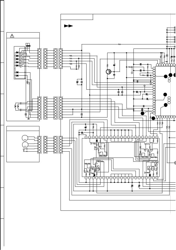
CD-M8000W/CP-M8000
A
|
PICKUP UNIT |
|
|
||
|
PICKUP |
|
|
|
|
|
HPC1LX |
|
|
|
|
B |
|
VCC |
7 |
7 |
|
|
|
||||
|
|
VREF |
|||
|
|
6 |
6 |
||
|
|
E |
|||
|
|
5 |
5 |
||
|
|
A |
|||
|
|
4 |
4 |
||
|
|
B |
|||
|
|
3 |
3 |
||
|
|
F |
|||
|
|
2 |
2 |
||
|
|
C |
|||
|
|
1 |
1 |
||
|
|
|
|||
|
|
|
|
CNS1B |
|
C |
|
|
|
|
|
|
|
TR– |
1 |
1 |
|
|
|
TR+ |
|||
|
TR+ |
2 |
2 |
||
|
|
||||
|
FO+ |
FO+ |
3 |
3 |
|
|
4 |
4 |
|||
|
FO– |
|
|||
D |
|
5 |
5 |
||
|
PD |
||||
TR– |
6 |
6 |
|||
|
VR |
||||
|
|
7 |
7 |
||
|
|
LD |
|||
|
|
8 |
8 |
||
|
GND |
||||
|
|
CNS2B |
|||
|
|
|
|
||
CD MOTOR PWB-D
|
M1 |
M |
+ |
6 |
6 |
|
SPINDLE |
SPIN |
|||
E |
MOTOR |
|
– |
5 |
5 |
|
|
+ |
|||
M2 |
|
4 |
4 |
||
|
|
||||
|
SLED |
M SLIDE |
3 |
3 |
|
|
MOTOR |
|
– |
2 |
2 |
|
SW4 |
|
PU-IN |
||
|
|
1 |
1 |
||
|
PICKUP IN |
|
|||
|
|
|
|||
|
|
|
|
CNP3A |
CNS3B |
F
G
CD SERVO PWB-C
|
|
|
|
CD SIGNAL |
|
|
|
|
|
|
|
|
|
|
|
|
|
|
|
|
|
|
|
|
|
|
|
|
|
C34 |
|
||||
|
|
|
|
|
|
|
|
|
|
|
|
|
|
|
|
|
|
|
|
|
|
|
|
|
|
|
|
|
|
|
|
|
C33 |
|
|
|
|
|
|
|
|
|
|
|
|
|
|
|
|
|
|
|
|
|
|
|
|
|
|
|
|
|
|
|
|
|
|
|
C32 |
|
|
|
|
|
|
|
|
|
|
|
|
|
|
|
|
|
|
|
|
|
|
|
|
|
|
|
|
|
|
|
|
|
|
|
C30 |
|
|
|
|
|
|
|
|
|
|
|
|
|
|
|
|
|
|
|
|
|
|
|
|
|
|
|
|
|
|
|
|
|
|
|
C57 |
|
|
|
|
|
|
|
|
|
|
|
|
|
|
|
|
|
|
|
|
|
|
|
|
|
|
|
|
|
|
|
|
|
|
|
C28 |
|
|
|
|
|
|
|
|
+B |
|
|
|
|
|
|
|
|
|
|
|
|
|
|
|
|
|
|
|
|
|
|
|
|
|
|
|
|
|
|
|
|
|
|
|
|
|
|
|
|
|
|
|
|
|
R7 |
|
|
|
|
|
|
|
|
|
|
|
|
|
|
|
C27 |
|
||
|
|
VCC |
|
|
|
|
|
|
|
|
|
|
|
|
47 |
|
|
|
|
|
|
|
|
|
|
|
|
|
|
|
C36 0.22/50 |
|
|||
7 |
7 |
|
|
|
|
|
|
|
|
|
+B |
|
|
|
|
+B |
|
|
|
|
|
|
|
|
|
|
+B |
C37 |
0.1 |
C35 |
|||||
6 |
6 |
VREF |
|
|
|
|
|
|
|
|
|
|
|
|
|
|
|
|
|
|
|
|
|
|
|
|
|||||||||
E |
R6 |
22K |
|
|
|
|
|
|
|
|
|
|
|
|
|
|
|
|
|
|
|
|
|
|
|
|
|
||||||||
5 |
5 |
|
|
|
|
|
|
|
|
|
|
|
|
|
|
|
|
|
|
|
|
|
|
|
|
R42 |
|||||||||
4 |
4 |
A |
R5 |
8.2K |
|
|
|
|
|
|
|
|
|
|
|
|
|
|
|
|
|
|
|
|
|
|
|
|
1.2K |
|
|
|
|
|
|
B |
R4 |
8.2K |
|
|
|
|
|
|
|
|
|
|
|
|
|
|
|
|
|
|
|
|
|
|
|
|
R41 12K |
R40 680 |
|
||||||
3 |
3 |
|
|
|
|
|
|
|
|
|
|
|
|
|
|
|
|
C5 |
|
|
|
R11 |
|
|
|||||||||||
F |
R3 |
22K |
|
|
|
|
|
|
|
|
|
|
|
|
|
|
|
|
|
|
|
|
|
||||||||||||
2 |
2 |
|
|
|
|
|
|
|
R9 |
|
|
C3 47/25 |
|
|
R10 |
0.047 |
|
|
|
10K |
|
|
|||||||||||||
|
|
C |
|
R1 |
|
R2 8.2K |
|
|
LASER DRIVER |
|
|
|
|
|
27K |
|
|
|
|
|
|
|
|
80 79 78 77 76 75 74 73 |
|||||||||||
1 |
1 |
|
|
|
|
|
3.3 |
|
|
|
|
|
|
|
|
|
|
|
|
||||||||||||||||
|
|
|
|
|
|
|
|
|
|
|
|
|
|
|
|
|
|
|
FR |
|
|
|
|
|
|
||||||||||
|
|
|
|
8.2K |
|
|
|
|
|
|
|
|
|
|
|
|
|
|
|
|
|
|
|
1 |
VVDD PCKIST |
|
|
PDO2 PDO1 |
|||||||
CNS1A |
|
CNP1 |
|
|
|
|
|
|
KTA1266GR |
|
|
|
|
|
|
|
C6 |
|
|
|
|
|
2 |
EFMINLDDLDS |
VVSS |
||||||||||
|
|
|
|
|
|
|
|
|
|
|
|
|
|
|
|
|
|
|
3 |
||||||||||||||||
|
|
|
|
|
|
Q1 |
|
|
|
|
|
TP3 |
0.1 |
|
|
|
|
|
|||||||||||||||||
|
|
|
|
|
|
|
|
|
C4 |
|
|
|
|
|
|
|
|
|
4 |
RF |
5 |
|
|
8 |
7 |
||||||||||
|
|
|
|
|
|
|
|
|
0.001 |
+B |
|
|
|
R12 |
|
C8 |
|
|
|
|
|||||||||||||||
|
|
|
|
|
|
|
|
|
|
|
|
|
|
|
|
|
5 |
RFVDD |
|
|
|
|
|
||||||||||||
|
|
|
|
|
|
|
|
|
|
|
|
|
|
330 |
0.0027 |
|
|
|
1 |
SLC |
|||||||||||||||
|
|
|
|
C1 |
|
|
|
|
|
|
|
|
|
|
|
|
|
|
|
|
|
|
|
|
|
|
|
6 |
RSVSS |
|
|
|
2 |
SLCI |
|
|
|
|
|
|
C2 0.01 |
|
|
|
|
|
|
|
|
|
|
|
|
|
|
|
|
|
|
|
|
|
7 |
FIN1 A |
|
|
|
||||
|
|
|
|
47/25 |
|
|
|
|
|
|
|
|
|
|
|
|
|
|
|
C50 |
|
|
TP1 |
|
|
|
|
|
|
|
|||||
|
|
|
|
|
|
|
|
|
|
|
|
|
|
|
|
|
|
|
|
|
|
8 |
FIN2 B |
|
|
|
|
|
|
||||||
|
|
|
|
|
|
|
|
|
|
|
|
|
|
|
|
|
|
|
|
22P(CH) |
|
TP2 |
|
|
|
|
|
|
|
||||||
|
|
|
|
|
|
|
|
|
|
|
|
|
|
|
|
|
|
|
|
|
|
9 |
TIN1 E |
|
|
|
|
|
|
||||||
|
|
|
|
|
|
|
|
|
|
|
|
|
|
|
|
|
|
|
|
|
|
|
|
|
|
|
|
|
|
|
|
LC7 |
|||
|
|
|
|
|
|
|
|
|
|
|
|
|
|
|
C52 |
|
|
|
|
|
|
|
|
|
C10 |
|
10 |
TIN2 F |
|
|
|
|
|||
|
|
|
|
|
|
|
|
|
|
|
|
|
|
|
|
|
|
|
|
|
|
|
|
10/50 |
11 |
VREF |
|
|
|
|
CD |
||||
|
|
|
|
|
|
|
|
|
|
|
|
|
|
|
0.001 |
|
|
|
|
C9 |
|
|
|
12 |
REF1 |
4 |
|
|
|
||||||
|
|
|
|
|
|
|
|
|
|
|
|
|
|
|
|
|
C53 |
|
|
|
|
|
|
|
|
|
|
|
|
||||||
|
|
|
TR– |
|
|
|
|
|
|
|
|
|
|
|
|
|
|
|
100/10 |
|
|
|
|
|
13 |
FE |
|
|
18 |
ADA |
|||||
1 |
1 |
|
|
|
|
|
|
|
|
|
|
|
|
|
|
0.001 |
|
|
|
|
|
|
|
|
|
14 |
TEC |
|
|
||||||
|
TR+ |
|
|
|
|
|
|
|
|
|
|
|
|
|
|
|
|
|
|
|
|
|
|
|
|
19 |
ADA |
||||||||
2 |
2 |
|
|
|
|
|
|
|
|
|
|
|
|
|
|
|
|
|
|
|
|
|
|
C11 |
|
15 |
TE |
|
|
||||||
|
FO+ |
|
|
|
|
|
|
|
|
|
|
|
|
|
|
|
|
|
C12 |
|
|
|
|
|
20 |
TDO |
|||||||||
3 |
3 |
|
|
|
|
|
|
|
|
|
|
|
|
|
|
|
|
|
|
|
|
0.22/50 |
16 |
RFMON |
6 |
|
|||||||||
|
FO– |
|
|
|
|
|
|
|
|
|
|
|
|
|
|
|
|
|
100P(CH) |
|
|
|
|
|
|
|
|
|
|||||||
|
|
|
|
|
|
|
|
|
|
|
|
|
|
|
|
|
|
|
|
|
|
17 |
JITTC |
|
|
|
|
|
|||||||
4 |
4 |
|
|
|
|
|
|
|
|
|
|
|
|
|
|
|
+B |
|
|
|
C54 |
|
|
|
+B |
|
|
|
|
SBCK/FG |
|||||
5 |
5 |
|
GND |
|
|
|
|
|
|
|
|
|
|
|
|
|
|
|
|
|
|
|
|
|
18 |
|
GPDAC CONT4 |
CONT5 |
|||||||
|
|
|
|
|
|
|
|
|
|
|
|
|
|
|
|
|
|
0.022 |
|
|
|
|
|
FDO SPDO SLDO |
|||||||||||
|
PD |
|
|
|
|
|
|
|
|
|
|
|
|
|
|
|
|
|
|
|
|
|
|
19 |
|||||||||||
6 |
6 |
|
|
|
|
|
|
|
|
|
|
|
|
|
|
|
|
|
|
|
|
2 |
|
|
|
||||||||||
|
VR |
|
|
C38 |
|
|
|
|
|
|
|
|
|
|
|
|
|
|
|
|
R13 1K |
|
20 |
||||||||||||
7 |
7 |
|
|
|
|
|
|
|
|
|
|
|
|
|
|
|
|
|
|
|
|
||||||||||||||
|
LD |
|
|
0.01 |
|
|
|
|
|
|
|
|
|
|
|
|
|
|
|
|
|
|
|||||||||||||
8 |
8 |
|
|
|
|
|
|
|
|
|
|
|
|
|
|
|
|
|
|
|
|
|
|
|
|
|
|
1 |
21 22 23 24 25 26 27 28 |
||||||
CNS2A |
|
CNP2 |
|
|
|
|
|
|
|
|
|
|
|
|
|
|
|
|
|
|
|
|
|
|
|
|
|
|
|
|
|
|
|
|
|
|
|
+B |
|
|
|
+B |
|
|
|
|
|
|
|
|
|
|
|
|
|
|
|
|
|
|
R14 |
R16 1K |
1K |
1K |
|
||||||
|
|
|
|
C39 |
|
|
|
|
|
|
|
|
|
|
|
|
|
|
|
|
|
|
|
|
|
|
|||||||||
|
|
|
|
|
R44 12K |
|
|
|
|
|
|
|
|
|
|
|
|
|
|
|
|
|
|
1K R151K |
|
||||||||||
|
|
|
|
100/10 |
|
|
|
|
|
|
|
|
|
|
|
|
|
|
|
|
|
|
|
|
|||||||||||
|
|
SP+ |
C40 |
220/6.3 |
MUTE 21 |
VREF |
STANDBY |
VCC |
SLDO |
SL+ |
|
SL– |
|
|
|
|
|
|
GND |
TR– |
TR+ |
FO– |
|
FO+ |
|
FD |
TO |
|
R17 |
R18 |
|
||||
6 |
6 |
|
|
20 |
19 |
18 |
17 |
16 |
15 |
14 |
13 |
12 |
11 |
10 |
9 |
8 |
7 |
6 |
5 |
4 |
3 |
|
2 |
1 |
|
|
|
|
|
|
|||||
SP– |
|
|
|
|
|
|
|
|
|
|
|
|
|
|
|
|
|
|
|
|
|
|
|
|
|
|
|
|
|
|
|
|
|||
5 |
5 |
|
|
|
|
|
|
|
|
|
|
|
|
|
|
|
|
|
|
|
|
|
|
|
|
|
|
|
|
|
|
|
|
||
SL+ |
|
|
|
|
|
|
|
|
|
|
|
|
|
|
|
|
|
|
|
|
|
|
|
|
|
|
|
|
|
|
|
|
|||
4 |
4 |
|
|
|
|
|
|
|
|
|
|
|
|
|
|
|
|
|
|
|
|
|
|
|
|
|
|
|
|
|
|
|
|
||
SL– |
|
|
|
|
|
|
|
|
|
|
|
|
|
IC2 |
|
|
|
|
|
|
|
|
|
|
|
|
|
|
|
|
|
||||
3 |
3 |
|
|
|
|
|
|
|
|
|
|
|
|
|
|
|
|
|
|
|
|
|
|
|
|
|
|
|
|
|
|
||||
PUIN |
|
|
|
|
|
|
+ |
|
|
|
|
|
|
|
|
|
|
|
|
|
|
|
|
|
|
|
|
|
|
|
|||||
2 |
2 |
|
|
|
|
|
+ |
|
|
|
|
M63001FP |
|
|
|
|
|
|
|
|
|
|
|
|
|
|
|
|
|
||||||
GND |
|
|
|
|
|
|
|
|
|
|
|
|
|
|
|
|
|
|
|
|
|
|
|
|
|
|
|
|
|||||||
1 |
1 |
|
|
|
|
|
|
|
|
|
|
FOCUS/TRACKING/ |
|
|
|
|
|
|
|
|
|
|
|
|
|
|
|
||||||||
|
|
|
|
|
|
|
|
+ |
|
|
|
|
|
|
|
|
|
|
|
|
|
|
|
|
|
|
|||||||||
CNS3A |
|
CNP3 |
|
|
|
|
|
|
|
|
|
|
|
SPIN/SLED DRIIVER |
|
|
|
|
|
|
|
|
|
|
|
|
|
|
|
||||||
|
|
|
|
|
|
|
|
|
|
|
|
|
|
|
|
|
|
|
|
|
|
|
|
|
|
|
|
|
|
|
|
DS1 |
|||
|
|
|
|
|
|
|
|
|
|
|
|
|
|
|
|
|
|
|
|
|
|
|
|
|
|
|
|
|
|
|
|
3 |
|
||
|
|
|
|
|
|
|
|
|
|
|
|
|
|
|
|
|
|
|
|
|
|
|
|
|
|
|
|
|
|
|
|
|
|
|
|
|
|
|
|
|
|
|
|
+ |
|
|
|
|
|
|
|
|
|
|
|
|
|
|
|
|
|
|
|
|
|
|
|
|
|
|
|
|
|
|
|
|
|
|
+ |
+ |
|
|
|
|
|
|
|
|
|
|
|
|
|
|
|
|
|
|
|
|
|
|
|
|
|
|
|
|
|
|
|
|
|
|
|
+ |
|
|
|
|
|
|
|
|
|
|
|
|
|
|
|
|
|
|
|
|
|
|
|
|
|
|
|
|
|
|
|
|
|
+ |
|
|
|
|
|
|
|
|
|
|
|
|
|
|
|
|
|
|
|
|
LD M– |
LD M+ |
|
|
|
|
|
|
|
|
|
|
|
|
|
22 |
23 |
24 |
25 |
26 |
27 |
28 |
29 |
30 |
31 |
32 |
33 |
34 |
35 |
36 |
37 |
38 |
39 |
40 |
|
41 |
42 |
|
|
|
|
|
|
||
|
|
|
|
|
|
|
VCC2 |
|
SPO |
SP+ |
SP- |
|
VCC3 |
|
|
|
|
|
|
|
|
|
M– |
|
M+ |
VCC4 |
|
|
|
|
|
|
|
|
|
|
|
|
|
|
|
|
|
|
|
|
|
|
|
|
|
|
|
C41 |
|
|
|
|
|
|
|
|
|
|
|
|
|
|
|
|
|
|
|
|
|
|
|
|
|
|
|
|
|
|
|
|
|
|
|
100/10 |
C46 |
|
|
|
|
|
|
|
|
|
|
|
|
|
|||
|
|
|
|
|
|
|
|
|
|
|
|
|
|
|
|
|
|
|
|
|
|
|
|
|
|
|
|
|
|
|
|
|
|
||
|
|
|
|
+B |
|
|
|
|
|
|
|
|
+B |
|
|
|
|
|
|
|
100/10 |
|
|
|
+B |
|
|
|
|
|
|
|
|
|
|
|
|
|
|
|
|
|
|
|
|
|
|
|
|
|
|
|
|
|
|
|
|
|
|
|
|
|
|
|
|
|
|
|
|
||
H
• NOTES ON SCHEMATIC DIAGRAM can be found on page 14.
|
1 |
2 |
3 |
4 |
5 |
6 |
Figure 18 SCHEMATIC DIAGRAM (1/10)
– 18 –
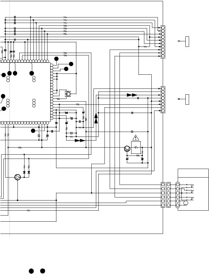
|
|
|
|
|
|
|
|
|
|
|
|
|
|
|
|
|
|
|
|
|
|
|
|
|
|
|
|
CD-M8000W/CP-M8000 |
||||||
|
|
|
|
C34 |
100P(CH) |
|
|
|
|
|
|
|
R38 |
|
1K |
|
|
|
|
|
|
|
|
|
|
|
|
|
|
|
|
|||
|
|
|
|
C33 |
0.022 |
|
|
|
|
|
|
|
|
R37 |
|
1K |
|
|
|
|
|
|
|
|
|
|
|
|
|
|
|
|
||
|
|
|
|
C32 |
100P(CH) |
|
|
|
|
|
|
|
R36 |
|
1K |
|
|
|
|
|
|
|
|
|
|
|
|
|
|
|
|
|||
|
|
|
|
|
|
|
|
|
|
|
|
|
|
|
|
R35 |
|
1K |
|
|
|
|
|
|
|
|
|
|
|
|
|
|
|
|
|
|
|
|
C30 |
100P(CH) |
|
|
|
|
|
|
|
R34 |
|
1K |
|
|
|
|
|
|
|
|
|
|
1 |
WRQ |
|
|
|
|
|||
|
|
|
|
C57 |
56P(CH) |
|
|
|
|
|
|
|
R33 |
|
1K |
|
|
|
|
|
|
|
|
|
|
2 |
DRF |
|
|
|
PWB |
|||
|
|
|
|
C28 |
100P(CH) |
|
|
|
|
|
|
|
R32 |
|
1K |
|
|
|
|
|
|
|
|
|
|
|
|
|
||||||
|
|
|
|
|
|
|
|
|
|
|
|
|
|
|
|
|
|
|
|
|
|
3 |
CE |
|
|
|
||||||||
|
|
|
|
|
|
|
|
|
|
|
|
|
|
|
|
|
|
|
|
|
|
|
|
|
|
|
|
|
|
|
|
|||
|
|
|
|
C27 |
0.022 |
+B |
|
|
|
|
|
|
|
|
|
|
|
|
|
|
|
|
|
+B |
|
|
4 |
DO |
|
|
CNS701 |
P23 12 - C FROM DISPLAY |
||
|
|
|
|
|
|
|
|
|
|
|
|
|
|
|
|
|
|
|
|
|
|
|
|
5 |
DI |
|
|
|||||||
|
|
|
|
|
|
|
|
|
|
|
|
|
|
|
|
|
|
|
|
|
|
|
|
|
|
|
|
|
|
|
||||
|
C37 |
0.1 |
C36 |
0.22/50 |
C35 0.047 |
|
|
|
|
|
|
|
|
|
|
|
|
|
|
|
|
|
|
|
|
|
6 |
CL |
|
|
||||
|
|
|
|
|
|
|
|
|
R29 |
|
|
|
|
|
|
|
|
R31 |
|
7 |
CD RES |
|
|
|||||||||||
|
|
|
|
|
|
|
|
|
|
|
|
|
|
|
|
|
|
8 |
CLAMP SW |
|
||||||||||||||
|
|
|
|
|
|
|
|
|
2.2K |
|
|
|
|
|
|
|
|
1K |
|
|
||||||||||||||
|
|
|
|
|
|
|
|
|
|
|
|
|
|
|
|
|
|
9 |
O/C |
|
|
|||||||||||||
R41 |
|
|
|
|
|
|
|
|
|
|
|
|
|
|
|
|
|
|
|
|
|
|
|
|||||||||||
12K |
|
|
|
|
|
R39 680 |
|
|
|
|
|
|
|
|
|
|
|
|
|
|
|
|
|
|
|
|
|
|
|
|
|
|||
R40 |
680 |
|
|
|
|
|
|
|
|
12 |
R28 |
|
|
|
|
|
|
|
|
|
|
10 |
DISC NO |
|
|
|
|
|||||||
|
|
|
|
|
|
|
|
|
|
|
|
|
|
|
|
|
|
|
|
|
|
|
|
|||||||||||
|
|
|
|
|
|
|
|
2.2K |
|
|
|
|
|
|
|
|
|
|
CNP8 |
|
|
|
|
|
||||||||||
77 76 75 74 73 72 71 70 69 68 67 66 65 64 63 62 61 |
|
|
|
|
|
|
|
|
|
|
|
|
|
|
|
|
||||||||||||||||||
|
|
|
|
11 |
|
|
|
|
|
|
|
|
|
|
|
|
|
|
|
|||||||||||||||
VVDD PCKIST |
|
|
PDO2 PDO1 |
CONT2 CONT3 |
VSS VDD5 DRF |
|
*WRQ |
DO |
DI |
|
60 |
|
|
|
|
|
|
|
|
|
|
|
|
|
|
|
|
|
|
|||||
VVSS |
*RES |
LRCKCLCE |
59 |
|
|
10 |
|
|
|
|
|
|
|
|
|
|
|
|
|
|
|
|||||||||||||
58 |
|
|
|
|
|
|
|
|
|
|
|
|
|
|
|
|
|
|||||||||||||||||
|
5 |
|
|
8 |
7 |
3 |
|
|
ASDFIN |
57 |
|
|
|
|
|
|
|
|
|
|
|
|
+B |
|
|
|
|
|
|
|
||||
|
|
|
|
ASDACK |
56 |
|
|
|
|
|
|
|
|
|
|
|
|
|
|
|
|
|
|
|
|
|||||||||
|
|
|
1 |
SLCO |
DATA 60 |
|
ASLRCK |
55 |
|
|
|
|
|
|
|
|
|
|
|
|
|
|
|
|
|
|
|
|
||||||
|
|
|
2 |
SLCIST |
BCK |
59 |
|
|
|
|
|
|
|
|
|
|
|
|
|
|
|
|
|
|
|
|
|
|||||||
|
|
|
|
16MOUT |
54 |
|
|
|
|
|
|
|
|
|
|
|
|
|
|
|
|
|
|
|
|
|||||||||
|
|
|
|
|
|
|
|
|
|
|
|
|
|
|
|
|
|
|
|
|
|
|
|
|
|
|
|
|
|
|
||||
|
|
|
|
|
|
|
IC1 |
|
|
|
|
EFLG |
53 |
|
|
|
XL1 |
|
|
|
|
|
|
|
|
|
|
|
|
|
|
|
|
|
|
|
|
|
|
|
|
|
|
|
|
|
C2F |
52 |
|
|
|
|
|
|
|
|
|
|
|
|
|
|
|
|
|
|
|
||
|
|
|
|
|
|
|
|
|
|
|
|
|
33.8688 MHz |
|
|
|
|
|
|
|
|
|
|
1 |
R-CH |
|
|
|
|
|||||
|
|
|
|
|
|
|
|
|
|
|
XVSS |
|
|
|
|
|
|
|
|
|
|
|
|
|
|
|
||||||||
|
|
|
|
|
LC78645NE |
|
|
|
51 |
|
|
|
|
|
|
|
|
|
|
|
|
|
|
2 |
AGND |
|
|
|
C PWB |
|||||
|
|
|
|
|
|
FSX/16MIN |
50 |
|
|
|
|
|
|
|
|
|
|
|
|
|
|
|
|
|
||||||||||
4 |
|
|
|
CD SERVO |
|
|
|
|
|
|
|
|
|
|
|
|
|
|
|
3 |
L-CH |
|
|
|
||||||||||
|
|
|
|
|
|
|
XIN |
49 |
|
|
|
|
|
|
|
|
|
|
|
|
|
|
|
|
CNS11 |
|||||||||
|
|
|
|
|
|
|
|
R43 |
|
|
|
|
|
|
|
|
|
|
|
|
|
|
P21 12 - FROM MAIN |
|||||||||||
|
|
|
|
|
|
|
|
|
|
|
|
|
|
|
|
|
|
|
|
|
|
|
|
4 |
DGND |
|
|
|||||||
|
|
|
ADAVDD |
|
|
|
|
XOUT |
48 |
|
|
|
|
+B |
|
|
|
|
|
+B |
|
|
|
|||||||||||
|
|
|
18 |
LVSS |
43 |
|
|
|
220 |
|
|
|
|
|
|
|
C42 |
|
D_5V |
|
|
|||||||||||||
|
|
|
|
|
XVDD |
47 |
|
|
|
|
|
|
|
|
|
5 |
|
|
||||||||||||||||
|
|
|
19 |
ADAVSS |
LCHO |
42 |
|
|
RVDD |
46 |
|
+B |
|
|
|
R22 |
|
|
|
|
|
0.01 |
|
|
6 |
A_5V |
|
|
||||||
|
|
|
20 |
TDO |
LVDD 41 |
|
|
|
|
ZD1 |
|
100 |
|
|
|
|
|
|
|
|
|
|
||||||||||||
|
6 |
|
|
|
RCHO |
45 |
|
|
|
|
|
|
|
|
|
|
|
7 |
D_GND (DRIVER) |
|||||||||||||||
|
|
|
|
|
|
|
|
|
|
|
|
DZ3.3BSB |
|
|
|
|
|
|
|
|
+B |
|||||||||||||
|
|
|
|
|
SBCK/FG |
DEFECT V/*P FSEQ |
|
|
|
|
RVSS |
44 |
|
C24 |
10/25 |
0.82 H |
|
|
|
|
|
8 |
+6.5V |
|
|
|
|
|||||||
GPDAC CONT4 |
|
|
|
|
|
|
|
|
|
43 |
|
|
|
|
|
|
|
|
|
|
|
|
|
|
|
|||||||||
CONT5 |
|
MONI1 MONI2 MONI3 |
MONI4 |
MONI5 |
|
VDD DOUT TEST |
|
|
|
C16 |
|
|
|
|
|
|
|
CNP7 |
|
|
|
|
|
|||||||||||
|
|
42 |
|
|
|
|
|
C51 |
|
|
|
|
|
|
|
|
||||||||||||||||||
|
VSS |
|
+B |
|
330/6.3 |
R25 |
|
|
|
|
|
|
|
|
|
|
||||||||||||||||||
|
41 |
|
|
|
0.022 |
|
|
|
|
|
|
|
|
|||||||||||||||||||||
|
0.001 |
|
|
|
2.2K |
|
|
|
|
|
|
|
|
|
|
|
|
|||||||||||||||||
24 25 26 27 28 29 30 31 32 33 34 35 36 37 38 39 40 |
C44 |
C23 |
|
C26 |
L1 |
|
|
|
|
|
|
|
|
|
|
|
|
|
||||||||||||||||
|
|
|
|
|
|
|
|
|
|
|
|
|
|
10/25 |
|
|
|
|
|
|
|
|
|
|
|
|
|
|
||||||
|
|
|
|
|
|
|
|
|
|
|
|
|
|
|
|
R24 |
|
0.0015 |
|
|
|
C48 |
|
|
|
|
|
|
|
|
|
|||
R16 |
1K |
1K |
1K |
|
|
|
9 |
|
|
|
|
|
|
C25 |
R27 |
|
|
0.022 |
|
|
|
|
|
|
|
|
|
|||||||
|
|
|
|
|
|
|
|
|
2.2K |
|
|
|
|
|
|
|
|
|
|
|
||||||||||||||
|
|
|
|
|
|
|
|
|
0.0015 |
|
|
|
|
|
|
|
|
|
|
|
|
|
|
|||||||||||
|
|
|
|
|
|
100/10 |
C22 |
|
|
10K |
|
|
|
|
|
|
|
|
|
|
|
|
|
|
||||||||||
|
|
|
|
|
|
|
|
|
C13 |
|
C14 |
|
|
|
|
|
|
|
|
|
|
|
|
|
|
|
|
|
|
|
||||
|
|
R17 |
R18 |
|
|
|
|
0.01 |
|
|
|
|
|
|
|
|
|
|
|
|
|
|
|
|
|
|
|
|||||||
|
|
|
|
|
0.022 |
|
|
|
|
|
|
|
|
|
|
|
|
|
|
|
|
|
|
|
|
|||||||||
|
|
|
|
|
|
|
|
|
|
R26 |
|
|
|
|
|
|
|
|
|
|
|
|
|
|
|
|
||||||||
|
|
|
|
|
|
|
|
|
|
|
|
|
|
|
|
|
|
|
|
|
|
|
|
|
|
|
|
|||||||
|
|
|
|
|
|
|
|
|
|
|
|
|
|
|
|
|
|
10K |
|
|
CONSTANT |
R51 |
|
|
|
|
|
|
|
|
||||
|
|
|
|
|
|
|
|
|
|
|
|
|
|
|
|
|
|
|
|
|
VOLTAGE |
|
|
|
|
|
|
|
|
|
||||
|
|
|
|
|
|
|
|
|
|
|
|
|
|
|
|
|
|
|
|
|
|
3.3 |
+B |
|
|
|
|
|
|
|
||||
|
|
|
|
|
|
|
|
|
|
|
|
|
|
|
|
|
|
|
|
|
|
|
|
|
|
|
|
|
|
|
|
|||
|
|
|
|
|
|
|
|
|
|
|
|
|
|
|
|
|
|
|
|
|
|
|
|
|
|
|
|
|
|
|
|
|
|
|
|
|
|
|
|
|
|
R20 |
|
|
|
|
+B |
|
|
|
|
|
|
|
|
+B |
KTC3203 Y |
|
|
(1/4W) |
R23 220 |
|
|
|
|
|
|
|
|
|
|
|
|
|
|
|
10K |
|
|
|
|
|
|
|
|
|
|
|
|
|
|
|
|
Fusible |
|
|
|
|
|
|
|
|||
|
|
|
|
|
|
|
|
|
|
|
|
|
|
|
|
|
|
|
|
|
Q2 |
C18 |
R47 |
|
|
|
|
|
|
|
||||
|
|
|
|
|
|
|
|
|
|
|
|
|
|
|
|
|
|
|
|
|
100 |
|
|
|
|
|
|
|
||||||
|
|
|
|
|
|
|
|
|
|
|
|
|
|
|
|
|
|
|
|
|
100/10 |
|
|
|
|
|
|
|
||||||
|
|
|
|
|
|
|
R46 |
R45 |
|
|
|
|
|
|
|
|
|
|
|
|
|
|
|
|
ZD2 |
|
|
|
|
|
|
|
|
|
|
|
|
|
|
|
|
|
|
|
|
|
|
|
|
|
|
|
|
|
|
|
DZ3.9BSB |
|
|
|
|
|
|
|
|||||
|
|
|
|
|
|
|
820 |
820 |
|
|
|
|
|
|
|
|
|
|
|
+B |
|
|
|
|
|
|
+B |
|
|
|
CD LOADING |
|||
|
|
|
|
|
|
|
D2 |
|
D1 |
|
|
|
|
|
|
|
|
|
|
|
|
|
|
|
|
|
|
|
||||||
|
|
|
|
|
|
DS1SS133 |
|
|
|
|
|
|
|
|
|
|
|
+B |
|
|
|
|
|
|
|
|
|
|
||||||
|
|
|
|
|
|
3 |
2 |
DS1SS133 |
|
|
|
|
|
|
|
|
|
|
|
|
|
|
+B |
|
|
CNS4 |
|
MOTOR PWB-E |
||||||
|
|
|
|
|
|
|
|
|
|
|
|
|
|
|
|
|
|
|
|
|
|
|
|
|
|
CNP4 |
|
|||||||
|
|
|
|
|
|
|
|
Q3 |
|
|
|
|
|
|
|
|
|
|
|
|
|
|
|
|
|
|
|
|
|
BI4 |
|
SW1 |
||
|
|
|
|
|
|
|
1 KRC102 M |
|
|
|
|
|
|
|
|
|
|
|
|
|
|
|
|
|
|
|
|
1 |
1 |
1 |
|
|
OPEN/CLOSE |
|
|
|
|
|
|
|
|
|
|
|
|
|
|
|
|
|
|
|
|
|
|
|
|
|
|
|
|
|
|
|
|
||||
|
|
|
|
|
|
|
|
|
|
|
|
|
|
|
|
|
|
|
|
|
|
|
|
|
|
|
|
|
|
|
|
|||
|
|
|
|
|
|
|
|
|
|
|
|
|
|
|
|
|
|
|
|
|
|
|
|
|
|
|
|
|
2 |
2 |
2 |
|
|
SW2 |
|
|
|
|
|
|
|
|
|
|
|
|
|
|
|
|
|
|
|
|
|
|
|
|
|
|
|
|
|
|
|
|
|
|
|
|
|
|
|
|
|
|
|
|
|
|
|
|
|
|
|
|
|
|
|
|
|
|
|
|
|
|
|
|
3 |
3 |
3 |
|
|
CLAMP |
|
|
|
|
|
|
|
|
|
|
|
|
|
|
|
|
|
|
|
|
|
|
|
|
|
|
|
|
|
4 |
4 |
4 |
|
|
SW3 |
|
|
|
|
|
|
|
|
|
|
|
|
|
|
|
|
|
|
|
|
|
|
|
|
|
|
|
|
|
5 |
5 |
5 |
|
|
|
|
|
|
|
|
|
|
|
|
|
|
|
|
|
|
|
|
|
|
|
|
|
|
|
|
|
|
|
|
+ M |
DISC Number |
||||
|
|
|
|
|
|
|
|
|
|
|
|
|
|
|
|
|
|
|
|
|
|
|
|
|
|
|
|
|
|
|
|
M3 |
||
|
|
|
|
|
|
|
|
|
|
|
|
|
|
|
|
|
|
|
|
|
|
|
|
|
|
|
|
|
6 |
6 |
6 |
– |
|
|
|
|
|
|
|
|
|
|
|
|
|
|
|
|
|
|
|
|
|
|
|
|
|
|
|
|
|
|
|
|
T/T UP/DOWN |
||||
|
|
|
|
|
|
|
|
|
|
|
|
|
|
|
|
|
|
|
|
|
|
|
|
|
|
|
|
|
|
|
|
|
||
|
|
|
|
|
|
|
|
|
|
|
|
|
|
|
|
|
|
|
|
|
+B |
|
|
|
|
|
|
|
|
|
|
|
LOADING MOTOR |
|
|
|
|
|
|
|
|
|
R49 |
|
|
|
|
|
|
|
|
|
|
|
|
+B |
|
|
|
|
|
|
|
|
|
|
|
|
|
|
|
|
|
|
|
|
|
1 |
|
|
|
|
|
|
|
|
|
|
|
|
|
|
|
|
|
|
|
|
|
|
|
|
|
|
• The numbers 1 to 12 are waveform numbers shown in page 37.
7 |
8 |
9 |
10 |
11 |
12 |
Figure 19 SCHEMATIC DIAGRAM (2/10)
– 19 –
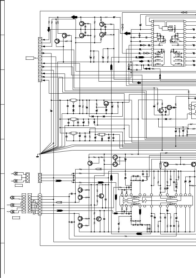
CD-M8000W/CP-M8000 |
|
|
|
|
|
|
|
|
|
|
|
|
|
|
|
|
|
|
|
|
|
|
|
|
|
|
|
|
|
|
|
|
|
|
|
|
|
|
|
|
|
|
|
|
|
|
|
|
|
|
|
|
|
|
|
|
|
|
|
|||||
|
|
|
|
|
|
|
|
|
|
|
|
|
|
|
|
|
|
|
|
|
SYSTEM |
R607 |
C613 |
|
|
|
|
IC601 |
|
|
|
|
|
|
|
|
|
|
|
|
|
|
|
|
|
|
|
|
|
|
|
|
|
|
|
|
|
|||||||
|
|
|
|
|
|
|
|
|
|
|
|
|
|
|
|
|
|
|
|
|
|
MUTE |
|
10/50 |
|
|
|
|
|
|
+B |
|
|
|
|
|
|
|
|
|
|
|
|
|
|
|
|
|
|
|
|
|
|
|
|
|
|
|||||||
|
|
|
|
|
|
|
|
|
|
|
|
|
|
|
|
|
|
|
|
|
|
|
|
|
10K |
|
|
|
|
|
LC75341 |
|
|
|
|
|
|
|
|
|
|
|
IC601 |
|
|
|
|
|
|
|
|
|
|
|
|
|||||||||
|
|
|
|
|
|
|
|
|
|
|
|
|
|
|
|
|
|
|
|
|
|
|
|
|
|
|
|
|
|
|
|
|
|
|
|
|
|
|
|
|
|
|
|
|
|
|
|
|
|
|
|
|
|
|
|
|||||||||
A |
|
|
|
|
|
|
|
|
|
|
|
|
|
|
|
|
R621 |
|
|
|
|
R613 |
|
|
|
|
|
|
AUDIO |
|
|
|
|
|
|
|
|
|
|
|
LC75341 |
|
|
|
|
|
|
|
|
|
|
|
||||||||||||
|
|
|
|
R609 |
|
|
|
|
|
|
|
|
|
|
|
|
|
|
|
|
560 |
R615 |
|
|
|
|
|
|
|
|
|
|
|
|
|
|
|
|
|
|
|
|
|
24 |
|
|
|
|
||||||||||||||||
|
|
|
|
|
|
|
|
|
|
|
|
|
|
|
|
2.2K |
|
|
|
|
|
|
|
|
|
|
PROCESSOR |
|
|
|
|
|
1 |
DI |
|
|
|
|
|
|
|
|
|
|
|
|
|
|
|
|
|
|
|
|||||||||||
|
|
|
|
|
330 |
|
|
|
|
|
|
|
|
|
|
|
|
|
|
|
|
|
|
2.2K |
|
|
|
|
|
|
|
|
|
|
|
|
|
|
|
|
|
|
|
|
CLK |
|
|
|
|
|
||||||||||||||
|
|
|
|
|
R610330 |
|
R868 |
6.8K |
R869 |
6.8K |
|
|
|
Q605 KTC3199GR |
|
|
|
|
R611 |
6.8K Q603 |
KTC3199GR |
|
|
|
C615 |
|
|
|
|
|
|
|
|
C606 |
|
|
|
|
|
2 |
CE |
|
|
|
|
|
|
|
|
|
|
|
|
VDD 23 |
+B |
|
|
|
||||||
|
|
|
|
|
|
|
|
|
|
|
C635 |
|
|
|
|
|
|
|
|
|
|
100/16 |
|
|
|
|
|
|
|
|
|
|
|
|
|
|
– |
|
|
|
|
|
|
C |
||||||||||||||||||||
|
|
|
|
|
|
|
|
|
|
|
0.001 |
|
|
|
0.001 |
|
|
|
|
|
|
|
|
|
|
|
|
|
|
|
|
|
|
|
|
|
|
|
|
|
|
|
|
|
|
|
|
|
|
|
|
|||||||||||||
|
|
|
|
|
|
|
|
|
|
|
|
|
|
|
|
|
|
|
|
|
|
|
|
|
|
|
|
|
|
|
VSS |
|
|
|
CCB |
|
|
+ |
|
|
|
VREF |
22 |
|
|
|
2 |
|||||||||||||||||
|
|
|
|
|
|
|
|
|
|
|
|
|
|
|
|
|
|
|
|
|
|
|
|
|
|
|
|
|
|
|
|
|
|
|
|
|
|
|
|
|
|
|
3 |
|
|
|
|
|
+ |
|
|
|
|
|
|
|||||||||
|
|
|
|
CNS901 |
|
|
KTC3199 GR |
|
|
Q863 |
|
|
|
|
|
C636 |
0.001 |
R612 |
|
|
|
|
|
|
C616 |
|
|
|
|
|
|
|
|
|
|
|
|
|
|
|
|
|
|
|
|
|
|
|
|
|
– |
|
|
|
|
|
|
|
|
|
|
|||
|
|
|
|
|
|
|
|
|
|
|
|
|
6.8K |
|
|
|
|
|
|
|
|
|
|
|
|
|
|
|
|
|
|
|
|
|
|
|
|
|
INTERFACE |
|
|
|
|
|
|
|
|
|
|
|
|
|||||||||||||
|
|
|
|
|
|
|
KTC3199 GR |
|
|
|
|
|
|
|
|
|
|
|
|
|
|
|
|
|
|
|
|
|
|
C609 |
|
|
LOUT |
|
|
|
ROUT 21 |
|
|
|
|
|||||||||||||||||||||||
|
|
|
|
|
Q862 |
|
R879 |
|
|
|
|
KTC3199GR |
|
|
|
0.001 |
|
|
|
|
|
|
|
|
|
|
|
|
|
4 |
|
|
|
|
|
|
|
|||||||||||||||||||||||||||
|
|
|
|
|
|
|
|
|
|
|
|
|
|
|
|
|
|
|
|
|
C607 |
|
|
|
|
|
|
|
|
|
|
|
|
|
|
C610 |
||||||||||||||||||||||||||||
|
|
|
|
L CH |
|
|
|
|
22K |
|
|
|
|
|
|
Q604 |
|
|
|
|
|
|
|
|
|
|
|
|
|
|
|
0.22 |
|
|
|
|
|
+ – |
|
|
|
|
|
|
|
+ – |
|
|
|
|
|
|
|
|||||||||||
|
|
|
|
|
|
|
|
|
|
|
|
|
R622 |
|
|
|
R616 |
|
|
|
|
|
|
|
0.22 |
|
|
|
|
|
|
5 |
|
|
|
|
|
|
|
|
|
|
|
|
|
|
20 |
|
|
0.22 |
||||||||||||||
|
|
|
1 |
|
|
|
|
|
|
|
Q606 |
R614 |
2.2K |
|
|
|
|
|
|
R605 |
|
|
|
|
LBASS |
|
|
|
|
|
|
|
|
|
|
|
|
|
|
|
|
|
|
|||||||||||||||||||||
|
|
|
|
|
|
|
|
|
|
2.2K |
|
|
|
|
|
|
|
|
|
|
|
|
|
|
|
|
|
|
|
|
|
|
|
|
|
|
|
RBASS |
|
|||||||||||||||||||||||||
|
|
|
|
|
|
|
|
|
|
KTC3199 GR |
|
|
560 |
SYSTEM |
|
|
|
|
|
|
3.9K |
|
|
|
|
|
|
|
6 |
|
|
|
|
+ – |
|
+ – |
|
|
|
|
|
19 |
|
|
|
|
||||||||||||||||||
|
|
|
|
|
A_GND |
|
|
|
|
|
|
|
|
|
|
|
|
|
|
|
|
|
|
|
|
MUTE |
|
|
|
|
|
|
|
|
|
|
|
|
|
|
|
|
|
|
|
|
|
|
|
|
|
|
|
|
|
|
|
|
|
|
|
|||
|
|
|
2 |
|
|
|
|
|
|
R878 |
|
|
|
|
|
|
|
|
|
|
|
|
|
|
|
|
|
|
|
|
|
C611 |
|
C619 |
|
|
LTRE |
|
|
|
|
|
|
|
|
|
|
|
|
|
|
RTRE |
|
C |
||||||||||
|
|
|
|
|
R_CH |
|
|
|
|
|
22K |
|
|
|
|
|
|
|
|
|
|
|
|
|
|
|
|
|
|
|
|
|
|
|
0.0015 |
|
|
1/50 |
|
7 |
LIN |
|
|
|
|
|
|
|
|
|
|
|
|
|
RIN 18 |
|
|
|
1 |
|||||
|
|
|
3 |
|
|
|
|
|
|
|
|
|
|
|
|
|
|
|
|
|
|
|
|
|
|
|
|
|
|
|
|
|
C621 |
|
|
|
|
|
|
|
|
|
|
|
|
|
|
|
|
|
|
|
|
|
||||||||||
|
|
|
4 |
|
LVL-CTRL |
|
|
|
|
|
|
|
|
|
|
|
|
|
|
|
|
|
|
|
|
|
|
|
|
|
|
|
|
10/50 |
|
|
|
|
|
8 |
LSEL0 |
|
|
|
|
|
|
|
|
|
RSEL0 17 |
|
|
|
|
|||||||||
|
|
|
|
|
|
|
|
|
|
|
|
|
|
|
|
|
|
|
|
|
|
|
|
|
|
|
|
|
|
|
|
C623 |
|
|
|
|
|
|
|
+ – |
|
|
|
+ – |
|
|
C624 |
|
||||||||||||||||
|
|
|
|
|
+B(16V) |
|
|
|
|
|
|
|
|
|
|
|
|
|
|
|
|
|
C617 2.2/50 |
|
|
|
|
|
|
|
|
|
|
|
|
|
|
|
|
|
L4 |
|
|
|
|
|
|
|
|
|
|
|
R4 |
|
|
|||||||||
B |
|
|
5 |
|
|
|
|
|
|
|
|
|
|
|
|
|
|
|
|
|
|
|
R619 |
22K |
|
|
|
|
|
|
|
|
1/50 |
|
|
|
|
|
|
9 |
|
|
|
|
AUX |
|
|
|
|
16 |
1/50 |
|
||||||||||||
|
|
|
|
|
|
|
|
|
|
|
|
|
|
|
|
|
|
|
|
|
|
|
|
|
|
|
|
|
C625 |
|
|
|
|
|
|
|
|
|
|
|
|
|
|
|
|
|
|
|
|
|
|
|||||||||||||
P24 2 - G |
|
GND(RECT) |
|
|
|
|
|
|
|
|
|
|
|
|
22/50 |
|
|
|
|
|
|
|
|
|
|
|
|
|
|
|
|
|
|
|
L3 |
|
|
|
|
|
|
|
|
|
|
|
R3 |
|
|
|
|
|||||||||||||
|
6 |
|
|
|
|
|
|
|
|
|
|
|
C618 |
|
R620 |
22K |
|
|
|
|
|
|
|
|
|
1/50 |
|
|
|
|
|
|
|
10 |
|
|
|
|
DECK |
|
|
|
|
|
|
15 |
|
|
|
|
||||||||||||||
|
|
|
|
|
|
|
|
|
|
|
|
|
|
|
|
|
|
|
|
|
|
|
|
|
|
|
|
|
|
|
|
|
|
|
|
|
|
|
|
|
|
|
|
|
|
|
|
|||||||||||||||||
|
CNP901 |
|
|
|
|
|
|
|
|
|
|
|
|
|
|
|
|
|
|
|
|
|
|
|
|
|
|
|
|
|
C627 |
|
L2 |
|
|
|
|
|
|
|
|
R2 |
C628 |
|
||||||||||||||||||||
|
7 |
|
|
|
|
|
|
|
|
|
|
|
|
|
|
|
|
|
|
|
|
|
|
|
|
|
|
|
|
|
|
|
|
|
|
|
|
|
|
|
|
|
|
|
||||||||||||||||||||
|
|
TO |
|
|
|
|
|
|
|
|
|
|
|
|
|
|
|
|
|
|
|
|
|
|
|
|
|
|
|
|
|
|
|
|
|
|
|
1/50 |
|
11 |
|
|
|
|
|
|
TUNER |
|
|
|
|
|
|
|
14 |
1/50 |
|
|||||||
|
|
|
|
M_+13V |
+B |
|
|
|
|
|
|
|
|
|
|
|
|
|
|
|
|
|
|
|
|
|
|
|
|
|
|
R617 |
|
|
C629 |
|
|
|
|
|
|
|
|
|
|
|
|
|
|
|
|
|
|
|||||||||||
|
POWER PWB |
8 |
|
|
|
|
|
|
|
|
|
|
|
|
|
|
|
|
|
|
|
|
|
|
|
|
|
|
|
|
|
|
|
L1 |
|
|
|
|
|
|
|
|
|
|
|
|
|
R1 |
|
|
|
|
|
|||||||||||
|
|
|
|
|
|
|
|
|
|
|
|
|
|
|
|
|
|
|
|
|
|
|
|
|
|
|
|
|
|
|
|
|
4.7K |
|
|
1/50 |
|
|
|
|
|
|
|
|
|
|
|
|
|
|
|
|
|
|
|
|
|
|||||||
|
|
|
|
|
–15V |
|
|
|
|
|
|
|
|
|
|
|
|
|
|
|
|
|
|
|
|
|
|
|
|
|
|
|
|
|
|
|
|
12 |
|
|
|
|
|
|
CD |
|
|
|
|
|
|
|
|
13 |
|
|
|
|
||||||
|
|
|
9 |
|
–B |
|
|
|
|
|
|
|
|
|
|
|
|
|
|
|
|
|
|
|
|
|
|
|
|
|
|
|
|
C642 |
|
|
|
|
|
|
|
|
|
|
|
|
|
|
|
|
|
|
|
|
C630 |
|||||||||
|
|
|
|
|
|
|
|
|
|
|
|
|
|
|
|
|
|
|
|
|
|
|
|
|
|
|
|
|
|
|
|
|
|
|
|
|
|
R624 |
|
|
|
|
|
|
|
|
|
|
|
|
|
|
|
|
|
|
||||||||
|
|
|
|
|
|
|
|
|
|
|
|
|
|
|
|
|
|
|
|
|
|
|
|
|
|
|
|
|
|
|
|
|
|
|
|
|
|
|
|
|
|
|
|
|
|
|
|
|
|
|
|
|
|
|
|
|
||||||||
|
|
|
10 |
M_GND(MTR) |
|
|
|
|
|
|
|
|
|
|
|
|
|
|
|
|
|
|
|
|
|
|
|
|
|
|
|
|
|
|
47P |
|
|
|
|
|
4.7K |
|
|
|
|
|
|
|
|
|
|
|
|
|
|
|
|
|
|
1/50 |
||||
|
|
|
|
|
|
|
|
|
|
|
|
|
|
|
|
|
|
|
|
|
|
|
|
|
|
|
|
|
|
|
|
|
|
|
|
|
|
|
|
|
|
|
|
|
|
|
|
|
|
|
|
|
|
|
|
|
|
|
|
|
|
|||
|
|
|
11 |
|
SP_RLY |
|
|
|
|
|
|
|
|
|
|
|
|
|
|
|
|
|
|
|
|
|
|
|
|
|
|
|
|
|
|
|
|
|
|
|
|
|
|
|
|
|
|
|
|
|
|
|
|
|
|
|
|
|
|
|
|
|
|
|
|
|
|
|
|
|
|
|
|
|
|
|
|
|
|
|
|
|
|
|
|
|
|
|
|
|
|
|
|
|
|
|
|
|
|
|
|
|
|
|
|
|
|
|
|
|
|
|
|
|
|
|
|
|
|
|
|
|
|
|
|
|
|
|
|
|
|
|
12 |
|
SP_DET |
|
|
|
|
|
|
|
|
|
|
|
|
|
|
|
|
|
|
|
|
|
|
|
|
|
|
|
|
|
|
|
|
|
|
|
|
|
|
|
|
|
|
|
|
|
|
|
|
|
|
|
|
|
|
|
|
|
|
|
|
|
|
|
|
|
|
|
|
|
|
|
|
|
|
|
|
|
|
|
|
|
|
|
|
|
|
|
|
|
|
|
|
|
|
|
|
|
|
|
|
|
|
|
|
|
|
|
|
|
|
|
|
|
|
|
|
|
|
|
|
|
|
|
|
|
|
|
13 |
|
SW+5V |
|
|
|
|
|
|
|
|
|
|
IC851 |
|
|
|
|
|
|
|
|
|
|
|
|
|
|
|
|
|
|
|
|
|
|
|
|
|
|
|
|
|
|
|
|
|
|
|
|
|
|
|
|
|
|
|
–20dBAT |
||||
|
|
|
|
+B |
|
|
|
|
|
|
|
|
|
|
|
|
|
|
|
|
|
|
|
|
|
|
|
|
|
|
|
|
|
|
|
|
|
|
|
|
|
|
|
|
|
|
|
|
|
|
|
|
|
|
|
|
|
|
S_MUTE |
|||||
|
|
|
|
|
|
|
|
|
|
|
|
|
|
|
KAI7812AP |
|
|
|
|
|
|
|
|
|
|
|
|
|
|
|
|
|
|
|
|
|
|
|
|
|
|
|
|
|
|
|
|
|
|
|
|
|
|
|
|
|
|
|
|
|
||||
|
|
|
|
|
|
|
|
|
|
|
|
|
|
|
|
VOLTAGE |
|
|
|
|
|
|
|
|
|
|
|
|
|
|
|
|
|
|
|
|
|
|
|
|
|
|
|
|
|
|
|
|
|
|
|
|
|
|
|
|
|
|
|
|
|
|||
C |
|
|
|
|
|
|
|
|
|
|
|
|
|
|
REGULATOR |
|
|
|
|
|
|
|
|
|
|
|
|
|
|
|
|
|
|
|
|
|
|
|
|
|
|
|
|
–B |
|
|
|
|
|
|
|
|
|
|
|
|
|
IC8 |
||||||
|
|
|
|
|
|
|
|
|
|
|
|
|
|
|
|
|
|
|
|
|
|
|
|
|
|
|
|
|
|
|
|
|
|
|
|
|
|
|
|
|
|
|
|
|
|
|
|
|
|
|
|
|
|
|
|
|
|
|
|
|
||||
|
|
|
|
|
|
|
|
|
|
|
|
|
|
|
|
|
|
|
|
|
|
|
|
|
|
|
|
|
|
|
|
|
|
|
|
|
|
|
|
|
|
|
|
|
|
|
|
|
|
|
|
|
|
|
|
|
|
|
|
R866 |
KIA4 |
|||
|
|
|
|
|
|
|
|
|
|
|
|
|
|
|
|
|
|
|
|
|
|
|
|
|
|
|
|
|
|
|
|
|
|
|
|
|
|
|
|
|
|
|
|
|
|
|
|
|
|
|
|
|
|
|
|
|
|
|
|
OPE |
||||
|
|
|
|
|
|
|
|
|
|
|
|
IC851 |
|
|
|
|
|
|
|
|
|
|
|
|
|
|
|
|
|
|
|
|
|
|
|
|
|
|
|
|
|
|
|
|
|
LD +7V |
|
|
|
|
|
|
|
|
|
330 |
|
|||||||
|
|
|
|
|
|
|
|
|
|
|
|
|
|
|
|
VOLTAGE |
|
|
|
|
|
|
|
+B |
|
|
|
|
|
|
|
|
|
|
|
|
|
|
|
|
|
|
|
|
|
|
|
|
|
|
|
|
|
|
|
|
|
|||||||
|
|
|
|
|
|
|
|
|
|
|
|
7812AP |
|
|
|
|
REGULATOR |
|
Q866 |
|
|
|
|
|
|
|
|
|
|
|
|
|
|
|
|
|
|
LVL-CTRL |
|
|
|
|
|
|
|
|
|
|
|
|
|
|
||||||||||||
|
|
|
|
|
|
|
|
|
|
|
18V |
1 |
|
3 |
|
|
|
|
|
|
|
+B |
KTC2026 |
|
|
|
|
|
|
|
|
|
|
|
|
|
|
|
|
|
|
|
|
|
|
|
|
|
|
|
|
|
|
|
|
|||||||||
|
|
|
|
|
|
|
|
|
|
|
|
|
0.047 R854 22K |
|
|
|
|
|
|
|
|
|
|
|
|
|
|
|
+B |
|
|
|
|
|
|
|
|
|
|
10/50 R870 |
|
|
|
|
|
|
|
|
|
|
|
|
|
|
|
|
|
|
|
|
|
|||
|
|
|
|
|
|
|
|
|
|
|
|
2 |
D858 1SS133 C851 |
C852 22/50 |
|
|
|
R860 |
|
|
|
|
|
|
|
|
|
|
|
|
|
|
|
|
|
|
|
1K |
|
|
|
|
R871 |
10K |
|
Q864 |
|
|
|
|
IC860 KIA4558P |
|
|
|
|
|||||||||
|
|
|
|
|
|
|
|
|
|
|
|
|
|
|
220 |
|
|
|
|
|
|
|
|
|
|
|
|
|
|
|
|
|
|
|
|
|
|
|
|
|
R880 |
|
|
|
|
|
||||||||||||||||||
|
|
|
|
|
|
|
|
|
|
C843 |
D859 1SS133 |
|
|
|
|
|
|
|
|
|
R859 |
|
|
|
|
|
|
|
|
|
|
|
|
|
|
|
|
KRC102 M |
|
|
|
|
|
|||||||||||||||||||||
|
|
|
|
|
|
|
|
|
|
|
|
|
|
|
ZD852 DZ8.2BSB |
C847 22/50 |
|
|
22K |
|
|
|
|
|
|
|
|
|
|
C899 |
|
|
|
|
10K |
|
|
7 |
|
|
||||||||||||||||||||||||
|
|
|
|
|
|
|
|
|
|
|
|
|
|
|
|
|
|
|
|
|
|
|
|
|
|
|
|
|
|
|
|
|
2 |
|
|
|
|
|
|
|||||||||||||||||||||||||
|
|
|
|
|
|
|
|
|
|
0.1 |
|
|
|
|
|
|
|
|
|
|
|
|
|
|
|
|
|
|
|
|
|
|
|
|
3 |
|
|
|
|
|
|
|
|
|
|
|
||||||||||||||||||
|
|
|
|
|
|
|
|
|
|
|
|
|
|
|
C849 |
10/50 |
|
|
|
|
|
|
|
|
|
|
|
|
|
|
|
|
|
|
|
|
|
|
|
|
|
D861 |
|
4 |
|
|
||||||||||||||||||
|
|
|
|
|
C856 |
|
|
|
|
|
|
|
|
|
|
|
|
|
|
|
|
|
|
|
|
|
|
|
|
|
|
|
|
|
C867 |
|
1 |
|
1SS133 |
|
|
|
|
|||||||||||||||||||||
|
|
|
|
|
3300/35 |
|
|
|
|
|
|
D852 |
|
|
|
|
|
|
|
|
|
|
|
|
|
|
|
|
Q865 |
|
|
|
1/50 |
|
|
|
|
|
|
1 |
|
|
||||||||||||||||||||||
|
|
|
|
|
|
|
|
|
|
|
|
|
|
|
|
|
|
|
|
|
|
|
|
|
|
|
|
|
|
|
|
|
|
|
|
|
|
|
|
|||||||||||||||||||||||||
|
|
|
|
|
KIA7810AP VOLTAGE REGULATOR |
|
|
|
|
IC852 |
|
|
|
|
|
1SS133 |
|
|
|
|
D857 |
LD+7V |
|
+B |
|
|
|
|
|
|
|
|
|
|
|
KTC3199 GR |
|
|
|
R873 |
|
|
|
|
|
|
|
|
|
|
||||||||||||||
|
|
|
|
|
|
|
|
|
KIA7810AP |
|
3 |
A_+10V |
+B |
|
|
|
|
|
|
|
1SS133 |
|
|
|
|
|
A_+10V |
|
+B |
|
|
|
|
|
|
|
|
|
|
|
|
|
|
|
1K |
|
|
|
|
|
|
|
|
|
|
|
||||||||
|
|
|
|
IC852 |
|
|
|
|
|
|
1 |
|
|
|
|
|
|
|
|
|
|
|
|
|
|
|
|
|
|
|
|
|
|
|
|
|
|
|
|
|
|
|
|
|
|
|
|
|
|
|
|
|
|
|
|
|||||||||
|
|
|
|
|
|
|
|
|
|
|
|
|
|
D851 1SS133 |
|
|
|
IC854 |
|
|
|
|
|
|
|
|
|
|
|
|
|
|
|
|
|
|
|
|
|
|
|
|
|
|
|
|
|
|
|
|
|
|
|
|
|
|
||||||||
D |
|
|
|
|
|
|
|
|
|
2 |
|
|
C853 |
47/25 |
|
|
|
|
|
|
|
|
|
|
|
|
|
|
|
|
|
|
|
|
|
|
|
|
|
|
D862 |
|
|
|
|
|
|
|
|
|
|
|
|
|
||||||||||
|
|
|
|
|
|
|
|
|
C855 0.1 |
C854 |
0.1 |
22K |
|
|
AN78L05 |
+BPROTECT |
|
+B |
|
|
|
|
|
|
|
|
|
|
|
|
|
|
1SS133 |
|
|
|
|
|
|
|
|
R881 |
|
|
|
|||||||||||||||||||
|
|
|
|
|
|
|
|
|
|
|
|
|
|
|
|
|
|
|
|
|
|
|
|
|
|
|
|
|
|
|
|
|
|
|
|
|
|
|
|
4.7K |
|
|
|
|||||||||||||||||||||
|
|
|
|
|
|
|
|
|
|
IC853 |
|
|
|
|
|
|
|
VOLTAGE |
D_+5V |
|
|
+B |
|
|
|
|
|
|
|
|
|
|
|
|
|
|
|
|
|
|
|
|
|
|
|
|
|
|
|
|
|
|
|
|
1 |
|||||||||
|
|
|
|
|
|
|
|
|
|
|
|
|
|
|
|
|
|
|
|
|
|
|
|
|
|
|
|
|
|
|
|
|
|
|
|
|
|
|
|
|
|
|
|
|
|
|
|
|
|
|
|
|
|
|
|
|
|
|
|
|||||
|
|
|
|
|
|
|
|
|
KIA7805AP |
|
+B |
|
|
REGULATOR |
A_+5V |
+B |
|
|
|
|
|
|
|
|
|
|
|
|
|
|
|
|
|
|
|
|
|
|
|
|
|
|
|
|
|
|
|
R867 |
||||||||||||||||
|
|
|
|
|
|
|
|
|
5V |
|
|
|
|
|
|
|
|
|
|
|
|
|
|
|
|
|
|
|
|
|
|
|
|
|
|
|
|
|
|
|
|
|
|
|
100K |
|||||||||||||||||||
|
|
|
|
GND(RECT) |
GND(REG) |
A GND(MUTE) |
A GND(A PRO) |
CD D GND M GND |
|
1 |
|
3 |
|
|
R853 R852 10K |
|
18V 1 |
|
|
3 |
|
SW_5.6V |
|
|
|
|
|
|
|
|
|
|
|
|
|
|
|
|
|
|
|
|
|
|
C864 22/50 |
R874 |
|
100K |
|
C863 22/50 |
R875 |
100K |
|
|
||||||||||
|
|
|
|
|
2 |
|
C857 47/25 |
|
C858 0.022 |
|
|
|
|
C845 |
0.047 |
|
|
|
|
|
|
|
|
|
|
|
|
|
|
|
|
|
|
|
|
|
|
|
|
|
|
|
|
|||||||||||||||||||||
|
|
|
|
C859 |
|
|
C869 10/50 |
|
|
|
2 |
|
C860 |
47/25 |
|
|
|
|
|
|
|
|
|
|
|
|
|
|
|
|
|
|
|
|
|
|
|
|
|
|
|
|
||||||||||||||||||||||
|
|
|
|
|
|
|
|
|
|
|
|
|
|
|
|
|
|
|
|
|
|
|
|
|
|
|
|
|
|
|
|
|
|
|
|
|
|
|
||||||||||||||||||||||||||
|
|
|
|
0.1 |
|
|
|
|
|
|
|
|
|
|
|
|
|
|
|
|
|
|
|
|
|
|
|
|
|
|
|
|
|
|
|
|
|
|
|
|||||||||||||||||||||||||
|
|
|
|
|
|
|
|
|
|
D863 |
|
|
|
|
+B |
|
|
|
|
|
|
|
|
|
|
|
|
|
|
|
|
|
|
|
|
|
|
|
|
|||||||||||||||||||||||||
|
|
|
|
|
|
|
|
|
|
|
|
|
|
CD_GND |
|
|
|
|
|
|
|
|
|
+B |
|
|
|
|
|
|
|
|
|
|
|
|
|
|
|
|
|
|
|
|
|
|
|
|
|
|
|
|
|
|
|
|
|
|||||||
|
|
|
|
|
|
|
|
|
|
|
|
|
|
|
|
|
|
|
1SS133 |
|
|
|
|
|
|
|
|
|
|
|
|
|
|
|
|
|
|
|
|
|
|
|
|
|
|
|
|
|
|
|
|
|
|
|
|
|
|
|
|
|||||
|
|
|
|
|
|
|
|
|
|
|
|
|
|
|
A_GND |
|
|
|
|
|
|
|
|
|
|
|
|
|
|
|
|
|
|
|
|
|
|
|
|
|
|
|
|
|
|
|
|
|
|
|
|
|
|
|
|
|
|
|
|
|||||
|
|
|
|
|
|
|
|
|
|
|
|
|
|
|
|
|
|
|
|
|
|
|
|
|
|
|
|
|
|
|
|
|
|
|
|
|
|
|
|
|
|
|
|
|
|
|
|
|
|
|
|
|
|
|
|
|
|
|
|
|
|
|||
|
|
|
|
|
|
|
|
|
|
|
|
|
|
D_GND |
|
|
|
|
|
|
|
|
|
|
|
|
|
|
|
|
|
|
|
|
|
|
|
|
|
|
|
|
|
|
|
|
|
|
|
|
|
|
|
|
|
|
|
|
|
|
|
|
||
|
|
LG1 |
|
|
|
|
|
|
|
IC853 |
|
|
|
|
|
|
|
|
|
|
|
|
|
|
Q110 |
|
|
|
R155 |
|
|
|
|
|
|
|
|
|
|
|
|
|
R156 |
220K |
|
|
|
|
|
|
REC_R |
|
|
|
||||||||||
|
|
|
|
|
|
|
|
|
|
|
|
|
|
|
R113 |
|
|
R114 |
|
|
KRC104 M |
|
|
150 |
|
|
|
A_+10V |
+B |
|
|
|
|
|
|
|
|
|
|
|
|
|
|
|
|
|
|
|
|
|
|
|||||||||||||
|
|
|
|
|
|
|
|
|
|
|
|
|
|
|
|
|
|
|
|
|
|
|
|
|
|
|
|
|
|
|
|
|
|
|
|
|
|
|
|
|
|
|
|
|
|
|
|
|||||||||||||||||
E |
|
|
|
|
|
|
|
|
|
KIA7805AP |
|
|
|
|
|
10K |
|
|
10K |
|
0V |
2 |
|
|
3 |
3.4V |
|
|
|
|
|
|
|
|
|
R |
|
|
|
|
|
|
|
|
|
|
|
|
|
|
|
|
|
|
|
|
|
|
|
|||||
|
BASE |
|
|
|
|
|
|
|
VOLTAGE |
|
|
|
|
|
|
|
|
|
|
|
|
|
|
|
|
|
|
|
|
|
|
|
|
|
|
|
|
|
|
|
|
|
|
|
|
|
|
|
|
|
|
|
|
|
|
|
||||||||
|
|
|
|
|
|
|
|
|
|
|
|
|
|
|
|
|
|
|
|
|
|
|
|
|
|
C153 |
|
|
|
|
|
|
|
|
|
|
|
|
|
|
|
|
|
|
|
|
|
|
|
|
|
|
MUTING |
|||||||||||
|
CHASSIS |
|
|
|
|
|
|
|
|
|
|
|
|
|
|
|
|
|
|
|
|
|
|
|
|
|
|
|
|
|
|
|
|
|
|
|
|
|
|
|
|
|
|
|
|
|
|
|
|
|
|
|
||||||||||||
|
|
|
|
|
|
|
|
|
REGULATOR |
|
|
9.3V |
|
|
|
|
|
|
R115 |
|
1 |
|
|
|
|
|
|
|
|
|
|
|
|
|
|
|
|
|
|
|
|
|
|
|
|
|
|
|
|
|
|
|
|
|
||||||||||
|
|
|
|
|
|
|
|
|
|
|
|
|
|
|
|
|
|
0V |
|
|
|
100/16 |
|
|
|
|
|
|
|
|
|
|
|
|
|
0V |
MUTING |
|
R154 |
|
R153 |
|
|
|
0V |
|||||||||||||||||||
|
|
|
|
|
|
|
|
|
|
|
|
|
|
|
|
|
|
|
8.6V |
|
|
|
|
4.7K |
1 |
|
|
|
|
|
|
|
|
|
|
|
|
|
|
|
|
|
|
|
|
|
|
|
|
|||||||||||||||
|
|
|
|
|
|
|
|
|
|
|
|
|
SWITCHING |
|
|
|
|
|
|
0V |
2 |
|
|
3 |
|
Q110,Q111: |
|
|
|
|
|
|
|
|
|
|
|
|
|
|
|
0.7V |
|
10K |
|
|
10K |
0.7V |
|
|
||||||||||||||
|
|
|
|
|
M GND |
(TAPE) |
|
|
|
|
|
|
|
|
Q109 |
|
|
|
|
|
|
|
|
|
|
|
|
|
|
|
|
|
|
|
|
|
|
|
|
|
|
|
|
|
|
|||||||||||||||||||
|
|
|
|
|
|
|
|
|
|
|
|
|
|
|
|
|
|
|
|
|
|
|
|
3.4V |
SWITCHING |
|
|
|
|
|
|
|
|
|
|
|
|
|
|
|
|
|
|
|
|
|
|
|
|
|
|
|
|
|
||||||||||
|
|
|
|
|
|
|
|
|
|
|
|
|
|
|
9.3V |
KTA1266 GR |
|
|
|
|
|
|
|
|
|
|
|
|
|
|
|
|
|
|
|
|
|
Q122 |
|
|
|
|
|
|
|
|
|
|
||||||||||||||||
|
|
|
|
|
|
|
|
|
|
|
|
|
|
|
|
|
|
|
|
|
|
|
|
|
|
|
|
|
|
|
|
|
|
|
|
0V |
|
|
|
|
|
|
|
Q121 |
|
0 |
||||||||||||||||||
|
|
|
|
|
|
|
|
|
|
|
|
|
|
R112 |
|
|
|
|
|
|
|
|
|
Q111 |
|
|
|
|
|
|
|
|
|
|
|
|
|
|
|
|
|
|
|
KTC3199 GR |
|
|
|
|
|
|||||||||||||||
R-CH |
|
|
|
|
|
|
|
|
|
|
|
|
|
|
|
|
|
|
|
|
|
|
|
|
|
|
|
|
|
|
|
|
|
|
|
|
|
|
|
|
|
|
|
|
|
KTC3199 GR |
|
|||||||||||||||||
|
|
|
|
|
|
|
|
|
|
C102 |
|
|
|
15K |
|
|
|
|
|
|
|
|
|
KRC104 M |
|
|
|
|
|
|
|
|
0.0022 |
|
|
|
|
|
|
|
|
|
|
|
|
|
|
|
|
|
|
|
|
|
|
|
|
|||||||
|
|
|
|
|
|
|
|
|
|
|
|
|
|
|
|
|
|
|
|
|
|
|
|
|
|
L |
|
|
R120 |
|
|
|
C120 |
C124 |
R132 |
5.6K 12K |
R134 |
|
|
|
|
|
|
|
R142 |
C136 100 |
|
|
|
R146 |
10K |
|
|
|
|
|
|
|
||||||
|
|
|
|
|
T1_R |
|
|
|
|
|
560P |
|
|
|
|
|
|
|
|
|
|
|
|
|
|
|
|
|
C118 |
68K |
|
|
|
|
|
|
|
|
|
|
|
|
|
|
|
|
||||||||||||||||||
|
1 |
T1_R |
|
|
|
|
|
|
|
|
|
|
|
|
|
|
|
|
|
|
|
|
|
|
|
|
|
560P |
|
|
|
|
|
|
|
|
|
|
|
|
|
|
|
|
||||||||||||||||||||
|
1 |
|
A_GND |
|
|
|
|
|
|
|
R102 |
|
|
|
|
|
|
|
|
|
|
|
|
|
|
56 |
0.033 |
|
|
|
|
|
|
|
C140 |
0.0033 |
|
|
|
|
|
|
|
|||||||||||||||||||||
L-CH |
2 |
A_GND |
2 |
|
|
|
|
|
|
|
|
|
1K |
|
|
|
|
|
|
|
|
|
|
|
|
|
C116 |
|
|
|
|
|
|
|
|
|
R126 |
R136 |
4.7K |
|
|
|
|
|
|
|
|
|
|
|
||||||||||||||
|
|
|
|
|
|
|
|
|
|
|
|
|
|
|
|
|
|
|
|
|
|
|
|
|
|
|
|
R122 |
|
|
|
|
|
|
|
|
|
|
|
|
|
|
|
|
||||||||||||||||||||
|
3 |
T1_L |
3 |
|
T1_L |
|
|
|
|
|
|
|
|
R101 |
|
|
|
|
|
|
|
|
|
|
|
|
|
100/25 |
|
|
|
|
|
|
|
|
|
|
0.022 |
C145 |
22/50 |
|
|
C146 |
220/10 |
|||||||||||||||||||
|
|
|
|
|
|
|
|
C101 |
|
|
1K |
|
|
|
|
|
|
|
|
|
|
R |
|
|
|
|
R174 |
1K |
100K |
R124 |
3.9K |
C122 |
|
|
R140 |
1.5K |
|
|
||||||||||||||||||||||||||
|
|
|
|
CNP101 |
|
|
|
|
|
|
|
|
|
Q104 |
|
|
|
|
|
|
|
|
|
|
|
|
|
|
|
|
|
|||||||||||||||||||||||||||||||||
|
|
|
|
|
|
|
|
|
|
|
|
|
|
|
|
|
|
|
|
|
|
|
|
|
R118 |
|
|
|
|
|
|
|||||||||||||||||||||||||||||||||
TAPE 1 |
|
|
|
|
|
|
|
|
|
560P |
|
|
|
|
|
|
|
|
|
|
|
|
|
|
|
|
|
1/50 |
|
|
|
|
||||||||||||||||||||||||||||||||
|
|
|
|
|
|
|
|
|
|
|
|
0V |
|
2SC1845F |
|
|
|
|
|
|
|
|
|
|
|
1KC112 |
|
C114 |
|
|
|
|
|
|
|
|
|
R138 |
6.8K |
|
C132 |
270P |
|
|
|
|
|
|
|
|
|
|
|
|
R158 |
|||||||||
PLAYBACK HEAD |
|
|
|
|
|
|
Q104,Q106: |
|
|
|
|
|
|
|
|
|
R108 |
|
|
|
|
|
|
|
330P |
|
|
|
|
|
|
|
|
|
|
|
|
|
|
|
|
|
|
|
|
|
|
|
||||||||||||||||
|
|
|
|
|
|
|
|
|
|
|
|
|
|
|
|
|
|
|
|
|
|
|
|
330P |
|
|
|
|
|
|
|
|
|
|
|
|
|
|
|
|
|
|
|
|
|
|
||||||||||||||||||
|
|
|
|
|
|
|
|
|
|
|
|
0.7V |
|
|
|
|
|
|
|
|
|
|
|
|
|
|
|
|
|
|
|
|
|
|
|
|
|
|
|
|
|
47/25 |
|
|
|
|
220 |
|||||||||||||||||
|
|
|
|
|
|
|
|
SWITCHING |
C106 |
|
|
|
|
|
|
|
47K |
|
|
|
|
|
|
|
|
|
|
|
|
|
|
|
|
|
|
|
|
|
|
|
C134 |
|
|
|
|
|
|
|
||||||||||||||||
F |
|
|
|
|
|
|
|
|
|
|
R104 |
|
|
|
|
|
|
|
|
R170 |
|
|
|
|
|
|
|
|
|
|
|
|
|
|
|
|
|
|
|
|
|
|
|
|
|
|||||||||||||||||||
CNS102 |
|
|
|
|
|
|
|
|
180P |
|
|
|
|
|
|
|
|
|
0V |
|
|
|
1K |
|
|
|
|
|
|
|
|
|
|
|
|
22/25 |
|
|
|
|
|
|
|
|
|
|
||||||||||||||||||
|
|
|
|
|
|
|
|
|
|
0V |
|
2.2K |
|
|
|
|
|
|
|
|
|
1K |
24 |
23 |
|
|
21 |
20 |
|
19 |
|
|
17 |
|
|
|
16 |
|
|
14 |
13 |
|
|
|||||||||||||||||||||
ERASE HEAD |
1 |
1 |
1 |
ERASE |
|
|
|
|
|
|
|
|
|
|
0.7V |
|
|
|
|
|
|
|
|
|
|
|
|
|
22 |
|
|
|
|
|
|
18 |
|
|
|
|
15 |
|
|
|
||||||||||||||||||||
|
M_GND |
|
|
|
|
|
|
|
|
|
|
|
|
|
|
|
|
|
|
|
|
|
|
|
|
|
– |
|
|
|
|
|
|
|
|
|
|
|
|
|
|
|
|
|
– |
|
|
|
|
|
|
|
|
Vcc |
|
|
||||||||
|
|
|
|
|
|
|
|
|
|
|
|
|
|
|
|
|
|
|
|
|
|
|
|
|
|
|
|
|
|
|
|
112K |
|
|
|
|
|
|
|
|
|
|
|
|
|
|
|
56K |
|
|
|
|
|
|
|
|||||||||
|
2 |
2 |
2 |
|
|
|
|
|
|
|
|
|
|
R106 |
|
|
|
|
0V |
|
|
|
|
|
|
|
|
|
|
+ |
|
|
|
|
|
|
|
IC101 |
|
|
|
|
+ |
|
|
|
|
|
|
|
|
|||||||||||||
|
T2_R2 |
|
|
|
|
|
|
|
|
0V |
|
|
|
|
|
|
|
|
|
|
|
|
|
|
|
|
Hich=T1 |
|
|
|
|
|
|
|
|
|
Hich=CHROME |
|
|
|
|
|
|
|
|
|||||||||||||||||||
|
|
|
|
|
|
|
|
|
|
|
|
|
|
3.3K |
|
|
|
|
|
|
|
|
|
|
|
|
|
|
|
|
|
|
|
|
|
|
AN7345K |
|
|
|
|
|
|
|
|
|||||||||||||||||||
R-CH |
3 |
3 |
3 |
A_GND |
|
|
|
|
|
|
|
|
|
Q106 |
|
|
R110 |
SWITCHING |
|
0V |
|
KTC3199GR |
|
560P |
|
|
|
|
|
R172 |
|
+ |
|
112K |
|
|
|
|
|
|
|
+ |
|
|
56K |
C142 |
ALC |
Nor/CrO2 |
|
ALC RIPPLE |
|
GND |
|
|
||||||||||
|
4 |
4 |
4 |
|
|
|
|
|
|
|
|
2SC1845F |
|
|
|
|
|
|
|
|
|
|
– |
|
|
|
|
|
|
|
|
|
|
|
|
|
|
|
|
|
– |
|
|
|
|
|
|
|
||||||||||||||||
|
|
T2_R1 |
|
|
|
|
|
|
|
|
|
|
|
|
|
4.7K |
|
|
Q108 |
|
C108 |
|
|
|
|
1 |
2 |
|
3 |
|
|
4 |
|
5 |
|
|
6 |
|
|
|
7 |
|
|
8 |
|
|
|
9 |
10 |
|
11 |
12 |
|
|
||||||||||
|
5 |
5 |
5 |
|
|
|
|
|
|
|
|
|
|
|
|
|
|
|
|
|
|
|
|
|
|
|
|
|
|
|
|
|
|
|
|
|
|
|
|
|
|
|||||||||||||||||||||||
L-CH |
|
|
|
|
|
|
|
|
|
|
|
|
|
|
|
|
|
|
|
R169 |
R171 |
1K |
|
|
|
|
|
|
|
|
|
|
|
|
|
|
|
|
|
|
|
|
|
|
|
|
|
|
|
|
|
|
|
|||||||||||
6 |
6 |
6 |
|
T2_L1 |
|
|
|
|
|
|
|
|
|
|
|
|
|
|
|
|
|
|
1K |
|
|
|
|
|
|
|
|
|
|
|
|
|
|
|
|
|
|
C133 |
|
|
|
|
|
|
|
|
|
|
|
|||||||||||
|
|
|
|
|
|
|
|
|
|
|
|
|
|
|
|
|
|
|
|
C111 |
|
|
|
|
|
|
|
|
|
|
|
|
|
|
|
|
|
22/25 |
|
|
|
|
|
|
|
|
|
|
||||||||||||||||
|
|
T2_L2 |
|
|
|
|
|
|
|
|
|
|
|
|
|
R109 |
4.7K |
|
|
|
|
|
|
|
|
|
|
|
|
|
|
|
|
|
|
|
|
|
|
|
|
|
|
|
|
|
|
|
|
|
|
|
|
|||||||||||
|
|
|
7 |
|
|
|
|
|
|
|
|
|
|
|
Q105 |
|
|
|
|
C107 |
560P |
|
|
330P |
|
|
C113 |
|
|
|
|
|
|
|
|
|
|
|
|
|
|
|
|
|
|
|
|
|
|
|
|
|
|
|
|
|
||||||||
|
|
|
|
|
|
|
|
|
|
|
|
|
0V |
2SC1845F |
|
|
0V |
|
|
|
|
|
R117 |
|
|
330P |
|
|
|
|
|
C127 0.022 |
|
|
R135 R137 |
6.8K |
|
|
|
|
R141 |
|
|
|
|
|
|
|
|
|
|
|
|
|||||||||||
|
|
|
|
|
|
|
|
|
|
|
|
|
|
|
|
|
|
|
|
|
|
|
|
|
|
|
|
|
R123 |
3.9K |
|
|
|
|
|
|
|
|
|
100 |
|
C141 |
|
|
|
|
|
|
||||||||||||||||
TAPE 2 |
|
|
|
|
|
|
|
|
|
|
|
C105 |
|
|
|
0.7V |
|
|
|
|
|
|
|
|
|
|
1K |
R173 |
|
|
|
|
|
|
|
|
|
|
|
|
|
|
|
|
|
|
||||||||||||||||||
|
|
|
BI102 |
|
|
|
|
|
|
|
|
|
|
|
|
|
|
|
|
|
|
|
|
|
|
|
|
|
|
|
|
|
|
|
C131 270P |
|
|
47/25 |
|
|
|
|
|
|
||||||||||||||||||||
RECORD/ |
|
|
|
|
|
|
|
Q103,Q105: |
180P |
|
|
|
|
R105 |
0V |
|
|
|
|
|
|
|
|
|
1K |
|
R121 |
|
R125 |
5.6K |
|
|
|
|
|
|
|
|
|
|
|
|
|
|
||||||||||||||||||||
PLAYBACK HEAD |
|
|
|
|
|
|
|
|
|
0V |
|
|
3.3K |
|
|
|
|
|
|
|
|
|
|
|
|
100K |
|
|
|
|
|
|
|
|
|
|
|
|
|
|
|
|||||||||||||||||||||||
|
|
|
|
|
|
|
SWITCHING |
|
|
|
|
|
0V |
|
|
C115 |
|
|
|
|
|
|
|
|
|
|
|
|
|
|
|
|
|
|
|
|
||||||||||||||||||||||||||||
|
|
|
|
|
|
|
|
|
|
|
|
|
|
|
0.7V |
|
R107 |
47K |
|
|
Q107 KTC3199GR |
SWITCHING |
100/25 |
|
|
|
|
|
|
|
|
|
|
|
|
C123 |
0.0022 |
C128 3.3/50 |
|
|
|
|
C135 |
0.022 |
|
|
|
R145 |
|
|
|
|
|
|||||||||||
G |
|
|
|
|
|
|
|
|
|
|
|
|
|
|
|
|
|
|
|
|
|
|
|
|
|
|
|
|
|
|
|
|
|
|
|
|
|
|
|
|
|
|
|
|||||||||||||||||||||
|
|
|
|
|
|
|
|
|
|
|
|
|
|
|
R103 |
|
|
R119 |
|
|
|
|
|
C117 |
C119 C121 |
|
|
|
|
|
C139 |
0.0033 |
|
10K |
|
|
|
|
|
|||||||||||||||||||||||||
|
|
|
|
|
|
|
|
|
|
|
|
|
|
|
|
|
|
|
|
|
|
0.033 |
560P 1/50 |
R131 |
12K |
4.7K |
R139 |
1.5K |
|
|
|
|
|
|
|
|
|
|||||||||||||||||||||||||||
|
|
|
|
|
|
|
|
|
|
|
|
|
0V |
|
|
2.2K |
|
|
|
56 |
|
|
|
|
|
|
|
|
|
|
|
|
|
|
|
|||||||||||||||||||||||||||||
|
|
|
|
|
|
|
|
|
|
|
|
|
|
|
|
|
|
|
|
|
|
|
|
|
|
|
|
|
|
|
|
|
|
|
|
|
|
|||||||||||||||||||||||||||
|
|
|
|
|
|
|
|
|
|
|
|
|
|
|
Q103 |
|
|
|
|
|
|
|
|
|
|
|
|
|
|
|
|
|
|
|
|
|
|
|
|
|||||||||||||||||||||||||
|
|
|
|
|
|
|
|
|
|
|
|
|
|
|
2SC1845F |
|
|
|
|
|
|
|
|
|
L |
|
|
|
|
|
|
|
|
|
|
|
|
|
|
|
IC101 |
|
|
|
|
|
|
|
|
|
|
|
|
|
|
|
|
|
|
|||||
|
|
|
|
|
|
|
|
|
|
|
|
|
|
|
|
|
|
|
|
|
|
|
|
|
|
|
|
|
|
|
R111 |
|
|
|
|
|
|
|
|
|
|
|
|
|
|
|
|
|
|
|
|
|
|
|
|
|
|
|
|
|
||||
|
|
|
|
|
|
|
|
|
|
|
|
|
|
|
|
|
|
|
|
|
|
|
|
|
|
|
|
|
|
|
15K |
|
|
|
|
|
|
|
|
|
|
AN7345K |
|
|
|
|
|
|
|
|
|
|
|
|
|
|
|
|
|
|||||
|
|
|
|
|
|
|
|
|
|
|
|
|
|
|
|
|
|
|
|
|
|
|
|
|
|
|
|
|
|
|
|
|
PLAYBACK AND RECORD/PLAYBACK AMP. |
|
|
|
|
|
|
|||||||||||||||||||||||||
H
• NOTES ON SCHEMATIC DIAGRAM can be found on page 14.
|
1 |
2 |
3 |
4 |
5 |
6 |
Figure 20 SCHEMATIC DIAGRAM (3/10)
– 20 –
 Loading...