

Page 1
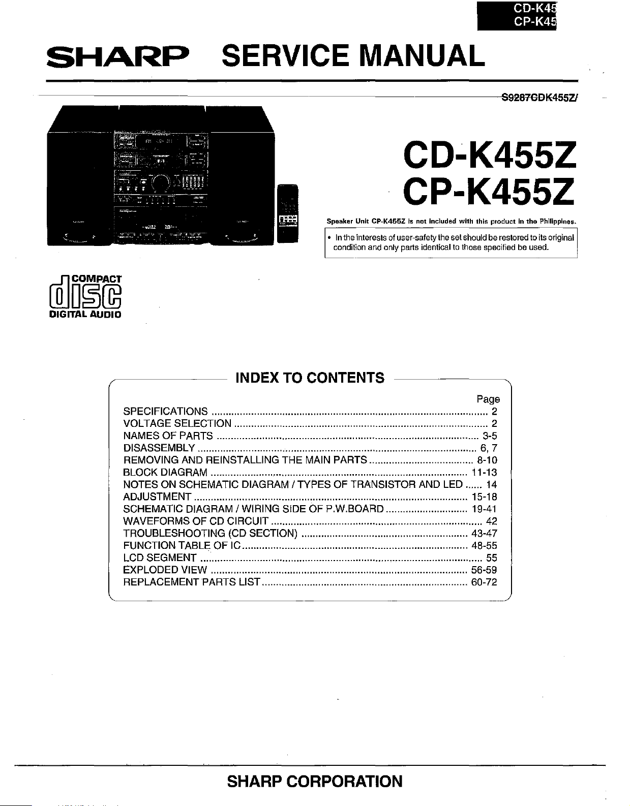
CD-K4
CP-K4
SHARP
---------------------------------~S92Il'1GDK:455Z1
SERVICE MANUAL
Speaker Unit CP-K455Zisnot included with this productinthe Philippines.
•Inthe
I
interestsofuser-safety
condition
and
only
parts
illJD~@
DIGITAL
AUDIO
CD-K455Z
CP-K455Z
the
set
identicaltothose
shouldberestored
specifiedbeused.
to
its
original
INDEX TO CONTENTS
Page
SPECIFICATIONS 2
VOLTAGE SELECTION 2
NAMES OF PARTS 3-5
DiSASSEMBLy
REMOVING AND REINSTALLING THE MAIN PARTS 8-10
BLOCK DIAGRAM 11-13
NOTES
ADJUSTMENT 15-18
SCHEMATIC DIAGRAM / WIRING SIDE OF P.W.BOARD
WAVEFORMS OF CD CIRCUIT
TROUBLESHOOTING (CD SECTION) 43-47
FUNCTION TABLE OF
LCD SEGMENT
EXPLODED VIEW 56-59
REPLACEMENT PARTS LIST 60-72
ON
SCHEMATIC DIAGRAM/TYPES OF TRANSISTOR AND LED
IC
'"
6,
14
19-41
42
48-55
55
7
SHARP CORPORATION
Page 2
-K455Z
-K455Z
FOR A COMPLETE DESCRIPTION OF THE OPERATION
TO
THE
CD-K455Z
• Mini component system
• General
AG
Power
source:
Power consumption:
Dimensions:
Weight:
• Amplifier section
Output power:
Output terminals:
Input terminals:
• Tuner section
Frequency range:
110/127/220/230-240
50/60
400
Width;
Height;
Depth; 347
9.1kg(20.0
PMPO;
MPO;
(10
% T.H.D. 1
RMS;
(10
% T.H.D. 1
Speakers;8ohms
Headphones;
(recommended;32ohms)
AUX;
MIG
FM;88(50/
SW2;
SW1;
MW;
(9
kHz
MW;
(10
kHz
OPERATION MANUAL.
Hz
W
270
mm
316
1,000 W (totai)
250
160 W
245
1/2;
100
9.50 - 21.85 MHz
3.20 - 7.30 MHz
531
span)
530
(10-5/6")
mm
(12-7/16")
mm
(13-11/16")
Ibs.)
W (125 W +
kHz,8ohms)
(80
kHz,8ohms)
16-50
mVl47
1 mVl4.7
108
MHz
kHz
span)
- 1,602
- 1,620
span)
V,
125
W +80W)
ohms
kohms
kohms
kHz
kHz
SPECIFICATIONS
• Cassette deck section
Tape:
Bia.s
and erasure
system:
Tape speed:
Heads:
Motor: DC
SIN
ratio:
Wow and flutter: 0.15 %
• Compact disc player section
Type:
Signal readout:
W)
Error correction:
Audio channels:
Decoder:
Filter:
Frequency response:
Wow and flutter:
CP-K455Z
• Speaker system
Type:
Maximum input
power:
Impedance:
Dimensions:
Weight:
OF
THIS UNIT, PLEASE REFER
Compact
AG
4.76 em/sec (1-7/8 ips.)
TAPE-l: Playback x 1
TAPE-2: Record/playback x 1
50
Compact
Non-contact,
conductor
eIRe
Solomon
2
16-bit
2~tjmes
and
20
Unmeasurable
(less
2-way 16
and5em
130
8
Width;
Height;
Depth;
4.6
cassette
Erase
motor
x 1
dB
(WRMS)
disc
laser
(Cross
Code)
linear
oversampling
active
filter
- 20,000
than
0.001%W.
em
(2")
W
ohms
180mm(7-3/32")
316
276.5
kg
(10.2 Ibs.)/each
3-beam
quantization
Hz
mm
tape
x 1
player
semi-
pickup
Interleave
(6-5/16") wooler
tweeter
mm
Reed~
digital
peak)
type
(12-7116")
(10-7/8")
(
\
(
filter
(
Specifications
notice.
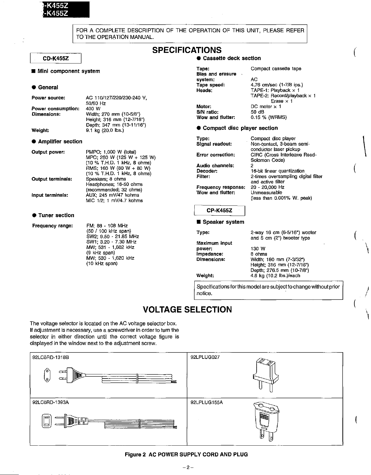
VOLTAGE SELECTION
The
voltage selector is located on the AC voltage selector box.
If adjustment is necessary, use a
seleclor
displayed in the window next to the adjustmenl screw.
92LG6RD·1318B
92LC6RD·1393A 92LPLUG155A
in
either direction untii the correct voltage figure is
screwdriver in order to turn the
92LPLUG027
Figure 2 AC POWER SUPPLY CORD AND PLUG
lor
this modelaresubject10change without prior
o
o
!
-2-
Page 3
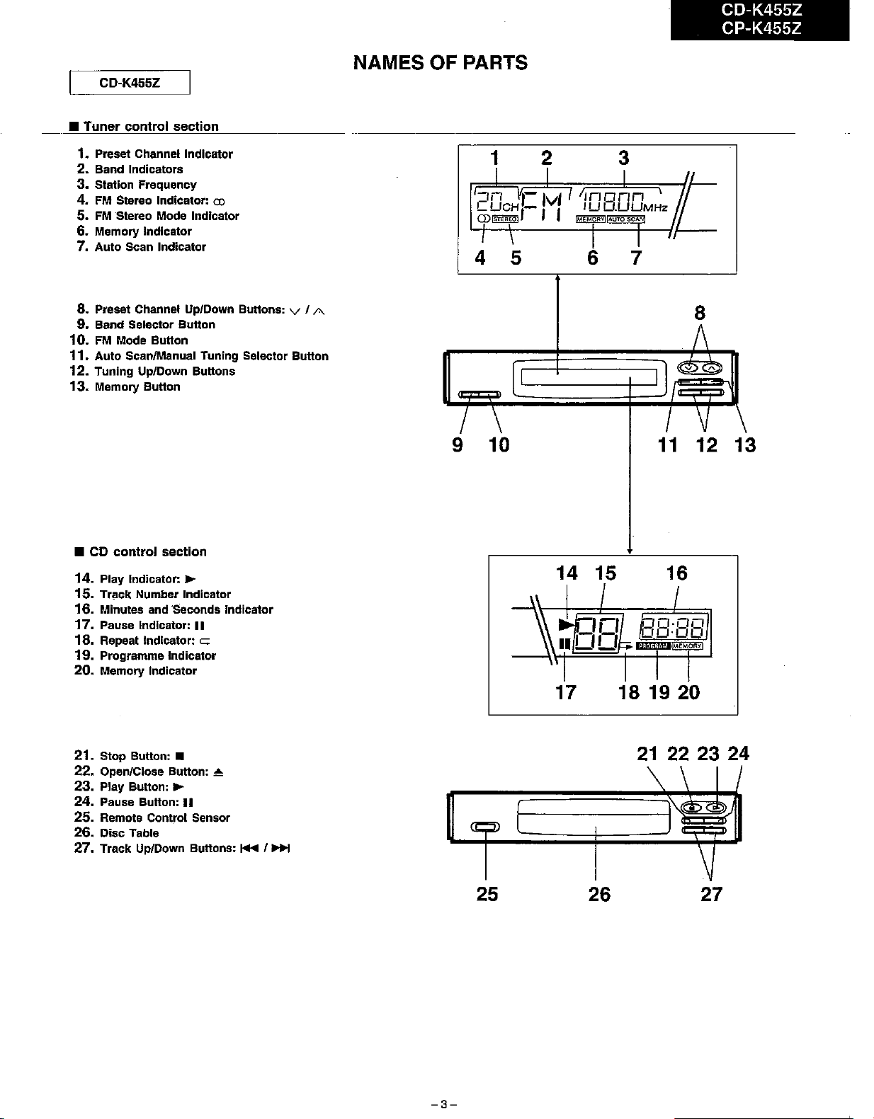
CD-K455Z
•
Tuner
control
1.
Preset Channel Indicator
2.
Band Indicators
3.
Station Frequency
4.
FM Stereo Indicator:
5.FMStereo Mode Indicator
6.
Memory Indicator
7.
Auto Scan
8.
Preset Channel Up/Down Buttons: v / A
9.
Band Selector Button
10.
FM
Mode Button
11.
Auto ScanlManual Tuning Selector Button
12.
Tuning UplDown Buttons
13.
Memory Button
section
CD
Indicator
NAMES OF PARTS
in
CUCH-
cpl[fffiQlf
I \ 1 I
4 5 6 7
[I'--
VII
Ivl"
"~~.
'Ina
IU
nn
.UUMHz
I,
+-_~
t
I
(v::>
CD-K455Z
CP-K455Z
""
•
CD
control
14.
Play Indicator:
15. Track Number Indicator
16.
Minutes and 'Seconds Indicator
17.
Pause Indicator:
18.
Repeat Indicator: c
19.
Programme Indicator
20.
Memory Indicator
21.
Stop Button: •
22.
Open/Close Button:
23.
Play Button:
24.
Pause Button:
25.
Remote Control Sensor
26.
Disc Table
27.
Track Up/Down Bullons:
section
~
II
~
~
II
i+lI/
~
11
12 13
14 15 16
/ I
21
222324
~
-3-
25 26
27
Page 4
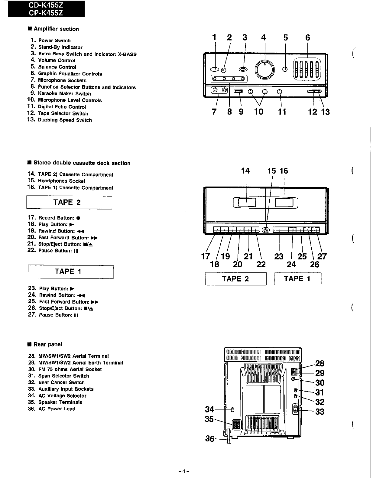
CD-K455Z
CP-K455Z
•
Amplifier
1. Power Switch
2. Stand-By Indicator
3. Extra Bass Switch and Indicator: X-BASS
4. Volume Control
5.
Balance Control
6. Graphic Equalizer Controls
7.
Microphone Sockets
8.
Function Selector Buttons and Indicators
9. Karaoke Maker Switch
10.
Microphone Level Controls
11. Digital Echo Control
12. Tape Selector Switch
13.
Dubbing Speed Switch
section
1 2 3 4
7 8 9 10
5 6
11
(
12 13
•
14.
15.
16.
Stereo
double
TAPE2)Casselle Compartment
Headphones Socket
TAPE 1) Casselle Compartment
cassette
TAPE 2
17.
Record BUllon: •
18.
Play Bullon:
19.
Rewind
20. Fast Forward
21. Stop/Eject
22. Psuse BUllon:
~
Bullon:
Bullon:
...
Bullon:
II/;!;
II
TAPE 1
23.
Play Bullon:
24.
Rewind
25.
Fast Forwsrd
26.
Stop/Eject
27.
Pause Button:
~
Button:
Bullon:
........
Bullon:
II/;!;
II
_
_
deck
seclion
TAPE 2
'-------~
14
15 16
I I TAPE 1
(
(
(
•
Rear
panel
28. MW/SW1/SW2 Aerial Terminal
29. MW/SW1/SW2 Aerial Earth Terminal
30,FM75
31. Span Selector Switch
32. Beat Cancel
33. Auxiliary Input Sockets
34.
35. Speeker Terminels
36.
ohms Aerial Socket
AC
Voltage Selector
AC
Power Lead
Switch
-4-
o~oooooooooooooooooooo
0000000
uoo~ooooooooo
34---tH~
[[]
35
36
ooooooooo~oooooooooooo
0000000000000
0000000
28
1lIl-IH-29
30
31
32
33
(
Page 5
CD-K455Z
CP-K455Z
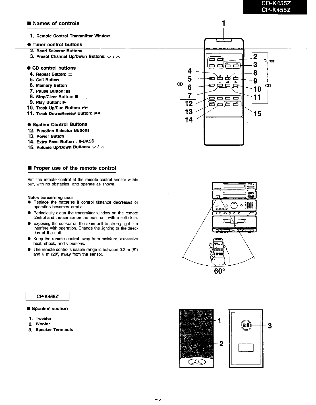
• Namesofcontrols
1.
Remote Control Transmitter Window
• Tuner control buttons
2~
Band Selector Buttons
3.
Preset Channel
•
CD
control buttons
4.
Repeat Bullon: c
5.
Call
Bullon
6.
Memory
7.
Pause Bullon:
8.
Stop/Clear Bullon: •
9.
Play Bullon:
10.
Track
11.
Track DownJReview Button:
• System Control Buttons
12.
Function Selector Buttons
13.
Power Button
14.
Extra Bass Bullon :
15. Volume UpJDown Buttons: v I A
•
Proper
Bullon
Up/Cue
useofthe
UplDown
1\
~
Bullon: _
Bullons: v / A
I'ttolIlI
X-BASS
remote
control
IT
CD 6
LL
12
13
14
1
21
3
Tuner
tI
10 CD
CJ
c:5
iiJ
15
Aim the remote control at the remote control sensor within
60°, with
Notes concerning use:
• Replace the batteriesifcontrol distance decreases or
• Periodically clean the transmitter window on the remote
• Exposing the sensor
• Keep the remote control away from moisture, excessive
• The remote control's usable rangeisbetween 0.2 m (8")
• Speaker section
1. Tweeter
2. Woofer
3. Speaker Terminals
no obstacles, and operate as shown.
operation becomes erratic.
control and the sensor on the main unit with a soft cloth.
on
interfere
tion of the unit.
heat, shock, and vibrations.
and 6 m (20') away from the sensor.
with
operation. Change the lighting or the direc-
the main unit to strong light can
I
..
0
I~
0
iim
00
=
@Jf--I+3
-5-
2
o
Page 6
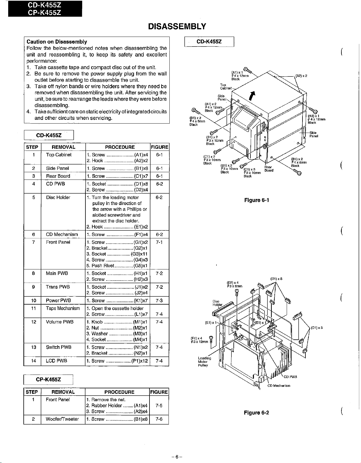
CD-K455Z
CP-K455Z
DISASSEMBLY
CautiononDisassembly
Follow the below-mentioned notes when disassembling the
unit and reassembling it, to keep its safety and excellent
pertormance~
1. Take cassette tape and compact disc out of the unit.
2. Be sure to remove the power supply plug from the wall
outlet before starting to disassemble the unit.
or
3. Take off nylon bands
wire holders where they need be
removed when disassembling the unit. After servicing the
unit, besure to rearrange the leadswhere theywere before
disassembling.
4. Takesufficientcare on staticelectricityofintegratedcircuits
and other circuits when servicing.
CD-K455Z
STEP
I
2 Side Panel
3 Rear Board
4
5 Disc Holder
REMOVAL
Top Cabinet 1.
CDPWB
PROCEDURE
Screw
2.
1.
1.
I.
2.
1.
.....................(AI )x4
Hook
.......................(A2)x2
Screw .....................(BI )x8 8·1
Screw .....................
Socket ....................
Screw
.....................(D2)x4
Turn the loading
pulley in
the arrow
the
with
(CI
(DI
motor
direction
a Phillips or
)x7
)x8
of
FIGURE
6-1
8-1
6-2
6-2
slotted screwdriver and
extract the disc holder.
2.
Hook
.......................
CD
6
7 Front Panel
8 Main PWB
9
10 PowerPWB 1. Screw .....................
11
12 Volume PWB 1. Knob ......................
13
14
Mechanism
Trans PWB
Tape
Mechanism
SwitchPWB
LCD PWB
I.
Screw
.....................
Screw
1.
2. Bracket ...................
3. Socket ..................
4.
5. Push Rive!.. ............ (G5)x1
I.
2.
1.Socket
2.
1.
2.
2. Nut .........................
3.
4.
1. Screw ..................... (N1)x2
2. Bracket ...................
1. Screw ...................
.....................
Screw
.....................(G4)x3
Socket .................... (HI
Screw
.....................(H2)x3
.....................
Screw
......................(J2)x4
Open
the cassette holder
Screw
......................(LI )x7
Washer
..................(M3)x1
Socket.................... (M4)x1
(EI)x2
(FI
)x4
(GI)x2
(G2)xI
(G3)xl1
)xl
(JI)x2
(KI)x7
(MI
)xl
(M2)xI
(N2)xl
(PI
)x'
6-2
7-1
7-2
7-2
7-3
7·4
7-4
7·4
7-4
2
CD-K455Z
1
W:
)X2
4x8mm
Black
(F1)x4
i63x12mm
Loading
Molor
Pulley
If:'l''
3x10mm
Black
it'l',
Black
Top
Cabinsl
t
'I
"W'"
W3X10mm
Black
(D2}x4
~3xBmm
4 x12mm
1f:'1<5
Black
1
3x
lOmm
Figure
6-1
Rear
Board
(D1)x5
(A2)x2
1
W
)X2
4x8mm
Black
Sida
Panel
(D1)x3
(
(
CP-K455Z
STEP
I
2 Wooferrrweeter
REMOVAL
Front
Panel
1.
Remove the
2.
Rubber
3.
Screw
I.
Screw
PROCEDURE
net.
Holder........
.....................(A2)x4
.....................
(AI)x4
(BI)x6
FIGURE
7-5
7-6
-6-
Figure
6-2
(
Page 7
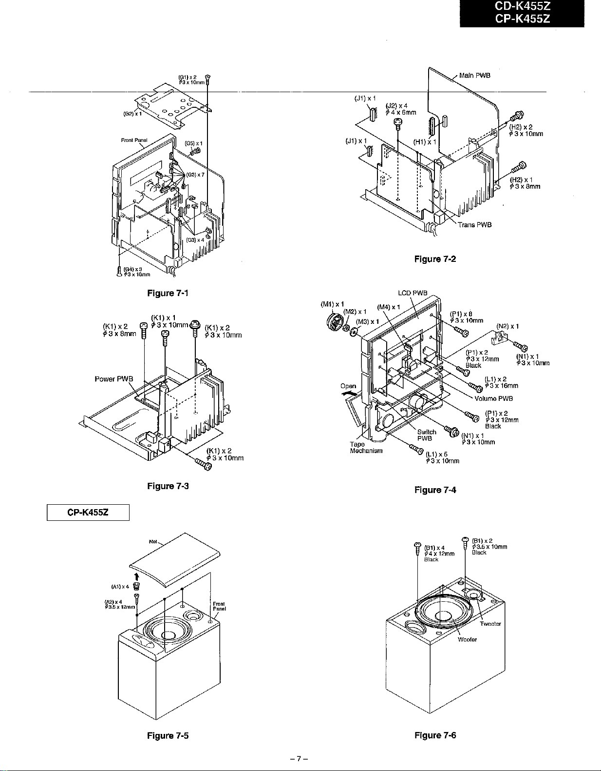
(G1)X2
f3x10mm
.--=~7'-"~-t--
---------------I------"'=--
CD-K455Z
CP-K455Z
(H2)
x2
tp3x
10mm
~
(H2) x 1
¢i3xBmm
CP-K455Z
(G4)x3
P3x10mm
Figure
Figure
No<
7-1
~3X10mm
7-3
(K1) x 2
(M1)x1 (M4)x1
~(M2)X1
f{JfI)4
(M3) x 1
Tape
Mechanism
Figure 7-2
LCDPWB
Figure 7-4
(L1) x 5
13 x
10mm
(B1)x4
914x12mm
Black
(N1) x 1
.p3x
10mm
(B1)x2
913.5x10mm
Black
(N2)
(L1)x2
13 x
16mm
(P1)x2
.p3x12mm
Black
x1
(N1) x1
13x
10mm
(A2)x4
i63.5x12mm
Figure 7-5
Figure 7-6
-7-
Page 8
CD-K455Z
CP-K455Z
REMOVING AND REINSTALLlNG THE MAIN PARTS
TAPE MECHANISM SECTION
Perform steps
to remove the tape mechanism.
How
erase heads (TAPE 2) (See Fig. 8-1.)
1.
Press the PLAY button to lift the head.
2. Remove the 2 screws (A1) to remove the record/playback
head.
3. Remove the 2 screws (A2) to remove the erase head.
Note:
Afterreplacing theheadsandcompletingtheazimuthadjustment,
be sure to apply screwlock.
Howtoremove the playback head (TAPE 1)
(See Fig. 8-2.)
1.
Press the PLAY button to lift the head.
2.
Remove the 2 screws (81) to remove the playback head.
to
remove
1,2,3,4,5,6,7
the
and11ofthe disassembly method
record I playback and
(A2)x2
If>
2x8mm
(A
1 )
rp2x7mm
Figure
xl
(
(A1)xl
';2x3mm
TAPE 2 I
Record/Playback
Head
8-1
TAPE 1 I
Note:
Afterreplacing the head and completing the azimuth adjustment,
be sure to apply screwlock.
Howtoremove the pinch roller (TAPE 1/2)
(See Fig. 8-3.)
1.
Carefully bend the pinch roller pawlinthe direction of the
arrow
® , and remove the pinch roller
Howtoremove
the
belt (TAPE 2)
(Cl)
upwards.
(See Fig. 8-4.)
1.
Remove the main belt (01) from the motor side.
2. Remove the FF/REW belt (02).
Pawl
[TAPE}]
(E
2)
FFIREW Selt
Figure 8-2
TAPE
t
Figure 8·3
Figure7-3
Motor
1/2
(C
Pinch Roller
(
1)
(
I TAPE 2
Howtoremove the belt (TAPE1)
(See Fig. 8-4.)
1.
Remove the tape 2 main belt (01) from the motor side.
2. Remove the tape 1 main belt
3. Remove the FF/REW belt (E2).
(El)
from the motorside.
-8-
Flywheel
(E
1)
Main Belt
(D
1)
Main Belt
Figure 8-4
Flywheel
Page 9
. CD-K455Z ' CD-K455Z
CP-K455Z CP-K455Z
How to remove the flywheel (TAPE 2)
(See Fig. 9-1.)
1.
Remove the belt.
2. Remove the screw (F1) to remove the pause kick lever.
3. Remove the stop washer (F2) with a small precision
screwdriver.
4.
Remove the washer (F3) upwards and extract the flywheel
from the capstan metal.
Note:
When the stop washer
nswans.
is
deformed or damaged, replace itwith a
How to remove the flywheel (TAPE 1)
(See Fig. 9-2.)
1.
Remove the belt.
2. Remove the stop washer (G1) with a small precision
screwdriver.
3.
Remove the washer (G2) upwards and extract the flywheel
from the capstan metal.
Note:
When the stop washer is deformed or damaged, replace It with a
newans.
o
Flywheel
I TAPE 1 I
(G
1)
Stop
Was:;h::e:-r
(G
2)
Washer
)
7
Flywheel
I
TAPE
2 I
Figure
----ll~
__
Ewasher
9-1
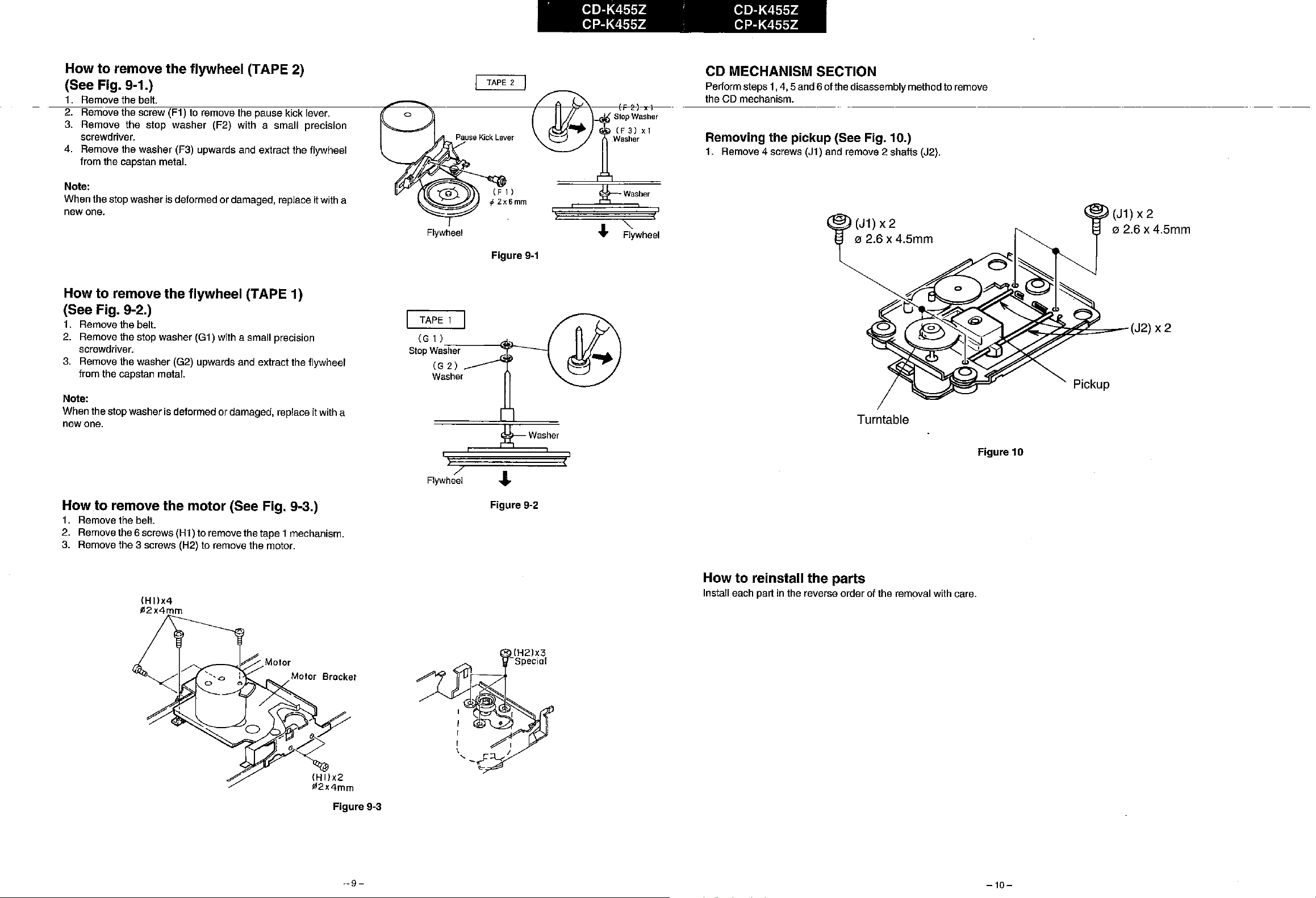
CD MECHANISM SECTION
Perform steps
the CD mechanism.
Removing the pickup (See Fig. 10.)
1.
Remove 4 screws (J1) and remove 2 shafts (J2).
Ewasher
"-
Flywheel
1
,
1,4,5
andSofthe disassemblymethod to remove
(J1)
x2
02.6
x 4.5mm
Turntable
~~~~S=-
Figure
10
Pickup
(J1) x 2
02.6
x4.5mm
(J2) x 2
How to remove the motor (See Fig. 9-3.)
1.
Remove the belt.
2. Removethe 6 screws (H1) to removethe tape 1mechanism.
3. Remove the 3 screws (H2) to remove the motor.
(H
Ilx4
¢2x4mm
Figure 9-3
I
,
I
\..,
-?~
.-
r'"
Figure 9-2
How to reinstall the parts
Install each partinthe reverse order of the removal with care.
pP,
/
-9-
-10-
Page 10
KEY
MATRIX
CD-K455Z CD-K455Z
CP-K455Z CP-K455Z
€f
----+Il , _ _
CD
Q229
Q230
I
I
INPUT
~~
I-I-_.;;~
~
L
R
: SELIlCTOR.R:ID
i
I R _
'''''''
P.'"'"'
60SS
IAUDIOI
le602
TCH52BP
FUNCTION
,;::,
GRAPIl]
63Hz
250Hz
~"t'
"t'
I L
L
~
L L
'""
_r.
~
..L
4-
RAMP
le6D3
BA4!i5BN
LINE
W r-"Ji
'J)-
I
.~
",.::'
t.v--
R I
C EQUAL I
I'Hz
"t'
ZEn
4-.Hz
l6~Hz
"t'
"t'
~
l.
lC701
8 ...
4558N
GEOIID---+B2
<i!
R
AMP
X-BASS
::::
..
"'"'"'
~
~VR706
1..
~
k..
__
~-B2
RID.
BALANCE
VOLUME
VR707
t t
E§+1l5
V:15~~:
07'
-1.
11:
+Bl
AUDIO
MUTING
ci:~~
l.G
~
L--
! +
6i.
L L
STK42iI5MKIl
R R
~
J901
4-.J
H~i1gb.
:'
-BI
~
I
"'"
'<:Y
PHONES
"eK
·SWITCH
k1--
IC,902
P~~R
~~L.AY
l""
~'"'J":O:'~'
..
.."J
IL
_----t
~~~;,]CONTROL
090
REI-AT
4-
(
-+j
""
IVD202-l!"
MW
~
T202
5W407,,s-'"
Tl
APSS
SOL40
I
~::'-
TI
APSSb
PLAYBACK
"
HEAD
=--"C····~l
'-"~
R-CH
--§.
RECORD/PLAYBACK
HEAD _~L
"
L-CH
-@_-"'.1."·__-----T
R-CH
~~.!'-~l
fil-
I!~E
HEAD ,
SWI ANT
_
SW[TCH[NG
I
I
I
SWITCHING SW[TCHING
,
I
I
L
i
--r-----.--<q;·"'='~=O,_
'
c
~
SW40 I
BEAT
CANSEL
I-
ANT
T206
r
SWI
OSC
-<Q;-;-;-;;;-]~
lIC405~+"
0,0,3101
Q413
sw
I
"'_A,'if
TAPI!
SELECTOR,
__
i!j4LLQ415SWITCHING-G
~.
::::
"''''''~
P·:MpEQ
" I
cl
~
g1~:
Q425
0430
BIAS
L411
FREQ.
Q421
BIAS
Q414
~
-
T"
"'"
R~
~~~~
1- ..
SWU4
T1
MUTING
SWITCHING
SW
ITCHING
(HIGH
SPEEol
",UT[NG
,~'"
Q499
SWITGHING
5W406
IC404
5A4558N
••
O;!'ilD<-1--1-t----;::=:::'-------------":'~~;~:~'~::'~~~======:(,-------------J
,
',~
If If
!.
.,L.
+B4
'"
SW801-SW808
IC80!
RH-IXI846AP
DATA/CLOCK/PRRIOD
IP
REO
SW405
--91
+84
T
'-=.
...
_u_'_'"_'
rf1
I
0402
Q407
Q4QS
~SWITCHING
I '
I i
Q543!
--------------~==I====I
.-_~
1 I
_,
C~~~~~L
loll
CROCOMPUTER
~
+B9
.....fl..
"""-./
LCDSOI
I'
,i
~+:~::::::+::::::::::::::::r~~~========~=F~~~~~~~~~~~~~~~~~~~~~~~===
!I!'
'I
L.-.(jR
II
~~C
,~+B4
0-423
M:;~:G
r.
\l
~539;
SWITCHING
L-----{'Q4101-----+1~~::I-----1
b
L
L
IC403
t<Y
BA3312N
~~~
R~--'"
I
I
+B4
0540
SWITCHING
Q4Q6
Il:::
-"
~
~
L
-
LBA14741:ID----+
_ :
I Q
I,
I
I
I
I I
I
i
1
I
, !
I
SWIM-A
TAPE
4
~
\<J
n
~
RBAI474IR[>
~
MIC
il!
~..!.!:'_---,
'
L L
I
-82
-<1:
ov-+
Lg
r-~~BA:~~8N
Il':f
i J
~
LJ2M VOLTAGE
MIC
SELECTOR
SWITCHING
d
~
__
b,.J
I
2 REGULATOR
I'Q5'3'3l
~1--''--(,,0053y
DUBBING
CONTROL I
...
[C50M
"".'
4
,,,.
,He
5FEED
~
~
,'"
~
~
L W--
'"
"'
T+:
+B2
MIC
h>-
~lh'
~1
,,-'i;;
MIC
LEVEL
SWITCHING
J
I
T'
T"
8 L L
.--~o<;jL
VR1M
I
rif-">J
-"-J'
,-l-;,=.,.,--il't
2
1"f
SPEED
~.
'---==t==------..J
~O'"
't
VR402 VR403
SFEED
CONTROL
~::::6
(j
R ANALOG R [j)
l"R
SW.
,IHi
~":<cr<~~:':;2::==t=~~
SWITCHING
r
~
DIGITAL
M50197F
Q51M Q52M
82
T'
1
-,~r~'~"~'~'~b--_J
BA4558N
7
--;-~~----
tD--_,
'"""
Q\
AMP
ECHO ~~MI-----<+"
IC3M
DIGITAL
ECHO.
Xli-I
tsr
Q"-~
~
1
SWITCHING
SWITCHING
M401
MOTOR
Q535
Q536
't
~"
I~
~br..l-+<--'---'-t+~+"
n~.T529D
I
RMC
L +
~@-@
~==="=.='='=====~
1
WSDl
__}-__
II
I
T'
L
R'"
~
ID--J
~
~
'1'
,'"
L L I I POWER
B~~::~N
BUFPER
"'RA"'P
R
I.t!
SWITCHING
I
SW~NG
~1.---4
I 7,
I'
J'
=__
:Jf-
J<>.
~~~r~KE
'<'>I
~AKER
050101
SWITCH[NG
'
__
,
~
Q531
Q532
SWITCHING
"
.
SW4Q3
T2
MOTOR
...
~.,.--l_
T1
MOTOR
...
~
LAMP 1
0603-0606
--,
~ITCHING
L-I_+
__
=j-1--r-:~
_±+~"~''-I0906
-'""""-i
<
Q603
-,--I
I Q6 04 -
L
l'
,.,,".,
....
·--l.--j----!-Q.;.1'I;';'=
+81
-81
'''l9V
I It:9EVkT911F\ ER{rRL:_O_:
I
<-l-J'-<~--M--
0907
VOLTAGE
'---t---{OQ8(4)--+--t,
RELAY
Q905
CONTROL
t--o'~~
: :
+--.o---ot~
L'=====ll:;-T-,"'","~{L
+a3
~~
-83
~
VOLTAGE VOLTAGE
REGULATOR REGULATOR
+84
+B5
+:~
2V
~:;~
I.--t--+--< { Q • T
~
""'"
,10917
+12VlMIIQ9lS
ILAMP I Q9 19
~
REGULATOR
--
~
VOLTAGE VOLTAGE
RECTIF[ER
D904-D907
'r
Q9l'
0915
R~~tl~~~R
--M--
-;:;.t=<j:J.''.'::-~J--------------'':T;f,
.~
Q920
REGULATOR
+5VlUN
SWITCHING
.f,~"""':'
-{j
FHoNo
S TUNER
TAPE
...
SWITCHING
ON/OFF
S~;~~~~Y
RELAY
[NO.
~+B7
1:
T901
~'="=:~:~:~:::="'='}_-:'~,~.~,-t'-'~~'-~~~~i:~-':v-~~-~~~-~_Rr
::::J
~
1'906
SWITCHeDI
'"
[e702
etE5~:
DM~IW:R
X-BASS
~+~7
Jr-fiI"ST5Z9DITH
~
'0'-_-';;
.;;o""""""-l;>~---<J
l
CS03
""
CONTROLLER
,l!':~,'.'
PiiWiiii
e~~
~
Q805
J.. J.. J..
1:1:~"f:.
LEo80l-LED804
PUNCTION
~
1'903
~.-9-~V--+-~
:
~~
m
SWS09-SWB14
SW901
"'''''
,0,
\{y
J
,II,
~
J.
IND.
220V
_~::~
RXSQI
REMOTE
SENSOR
:)
1'90
[NO
AC
ftx
I
110/127/
22lJ/230-240V
SO/60Hz
i<:?
& R
GND
GND
SPIlAKI!RS
(
(
(
-11
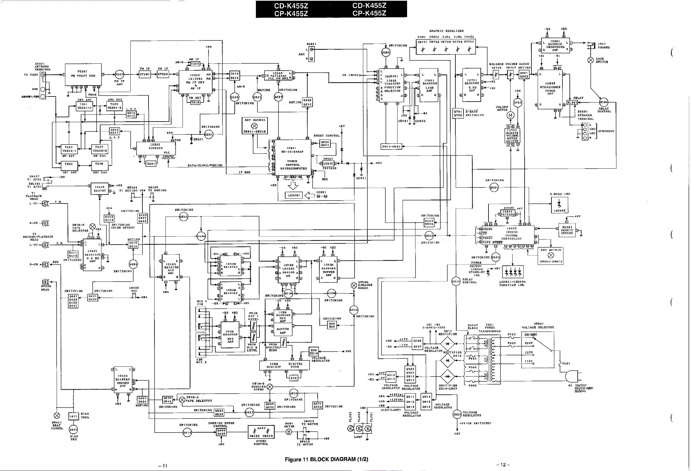
Figure11BLOCK
DIAGRAM (1/2)
-12-
Page 11
CD-K455Z CD-K455Z
CP-K455Z CP-K455Z
NOTES ON SCHEMATIC DIAGRAM
PICKUP
-------'F~f_-----
UNIT
*}I==='''''=::=WimD==:=~t~'b':==''ve,==:>{
"'C'
T~NGr---I--tJ.J~,v!===~=+~J~"v=~1
~
......
H::Ji;lAjJee"oJ!---{DO
"'
MI
M
PICKUP
SWl
c-
LOADING
MOTOR
M'
MMr--t--+--------~--.J
.......
DISC
m
M
HOLDER
SLID!!
MOTOR
IN
CA'"
DRIVER
MOTOR
'"
M54-64-1I..
CDMING
DRIVER
VRl
FOCUS
GAIN
Vfl2
TRACKING
-------+---<I'--~~.___+----I__x._-.--
OFFS8T
1 i Ie> 1
A1--
f"[i,
}-----------------,
~CNSiA"T
VOLTM"
I,
INPUi
.{(D-ItIJlCU'i~;:umm
I
l(
11:01G,,'i!],~~[[B'lG:.I"""""""l
....'I,
---;:::::::;
L--<~\>-,
.I.
[1'>-
;mr
lDO
LA6515
SPIN/SLIDE
1 V
..
~'-
0
l'
~,"",,"",
~
Jmm
':}
('"
••
0;" 7
---'
I R:DUT vee 8
-8V
n=JA-f
l.
,
!
rFr~~~~~~~~~~~~~~~==I~D~'l-J_r_
Bels
oc,
e
"
---<
'----
" ''"0
•
TSTOUT
ICIO
I
BA4SS'8
BUFFER
AMP
o 0 MUTING
L£UT',7
VR3
POCUS
OPFSE~R~~ilNG
VRS
TRACK
I NG
GAIN
ERROR
BALANCE
')¢=:>{
;
'::::.:'
'tdDI-:t!
Y1~IHO
OOHTOOL
M
H
REGISTE.
..
L,,~JLEYEL
1'1
I
HV
+7.3V
;'f~
VOD
,
0"
I
","
OUT
~~1
,,,
I'"
""
T T
,-,."'"
I
,,,
r r
SHIFT~
DAt
'-
,.
n--l
lOI
,
0102
DE-EMPHASIS
0105"
®D
1 R:DUT vee
8V
Pl:-JU
• Resistor:
To
differentiate the unitsofresistors, such symbolasK and
_~~OVIDI
CLOCK
"'
'"
~
mVD/><
'""
::::;
~
-----
---
l"1~ilI''fJ~~'iJ!t1
11
,
0"
fr:H'
OUT
,
~L£YEL
..-.l
,p
J,:...
,
""
'"
"-STRING
j..\-
",
SH'FT~
OAt
r"
+5"VIDl
I
C1
02
BA45"58
L. P. P
£.X~o"'",rq
10.
LC9600AM
D/A
CONVERTER
HV
+7.3V
,';----I~:~
TO
AUDIO
CO
SIGNAL
M are used: the symboi
--
--M
means 1000 kohm and the resIstor without any symbol
ohm-type resistor. Besides, the one with "Fusible" is a fuse
type.
• Capacitor:
To
indicate the unit of capacitor, a symbol
symbolPmeansmicro-micro-faradand theunit
without suchasymbolismicrofarad.Astoelectrolyticcapacitor,
the expression "capacitancelwithstand voltage" is used.
(CH), (TH), (RH), (UJ): Temperature compensation
(ML): Mylar type
(P.P.): Polypropylene type
• Theindicatedvoltage in each section is the
Digitai Multlmeter between such a section and the chassis
with no signal given.
REF.
NO
SW1
SW1MA
SW1MB
SW2
SW50M
SW201
SW401
SW402
SW403
SW404
SW405
SW406
SW407
SW801
SW802
SW803
SW804
DESCRIPTION
PICKUP
TAPE
DUBBING
DISC
KARAOKE
SPAN
BEAT
TAPE1MOTOR
TAPE2MOTOR
TAPE1MUTING
TAPE2MUTING
TAPE2RECORD
APSS
BAND
FMMODE
TUNER
TUNER
K means 1000 ohm and the symboi
one
POSITION
IN
SELECTOR
SPEED
HOLDER
MAKER
SELECTOR
CANCEL
DOWN
UP
OFF
NORMAL
NORMAL
CLOSE
ON
50/9
A
OFF
OFF
OFF
OFF
OFF
OFF
OFF
OFF
OFF
OFF
Pis
used: this
olthe
capacitor
measured by
1.
Tuner:
():
MW/SW1/SW2 mode
():
IS
Marking except for
2.
CD
():
Play mode
Marking except for
3. Deck section
():
Record mode
Marking except for
DisplayI Control section:
( ):Active state
Marking except for
Schematic Diagram and Wiring Side of P
•
model are subject to change
notice.
•
Partsmarkedwith "
the safety of
specifiedones
the set.
REF.NO
SW805
SW806
SW807
SW808
SW809
SW810
SW811
SW812
SW813
SW814
SW851
SW852
SW853
SW854
SW855
SW856
SW901
the
set. Be sure to replace these parts with
for
maintaining the safety and performance of
DESCRIPTION
AUTO/MANUAL
MEMORY
PRESET
PRESET
POWER
X-BASS
CD
TUNER
TAPE
AUX
OPEN/CLOSE
CD
PLAY
CD
STOP
CD
PAUSE
CD
UP(»I)
CD
DOWN(~)
VOLTAGE
FM mode
():
Stop state
():
Playback
():
CD Function
Lt,;'
(
DOWN
UP
SELECTOR
mode
mode
for
improvement without prior
I)
areimportantformaintaining
POSITION
OFF
OFF
OFF
OFF
STAND-BY
OFF
OFF
OFF
OFF
OFF
OFF
OFF
OFF
OFF
OFF.
OFF
230-240V
':<
';
~QQr_'
at stop state
W.Board
:':;:,~_
lqtfl
:;-l:JI\/l~2
__
for
this
o
~-~
g/9
TO
LCD80l
~,~.",
,{
"
RES!!T
~
IC851
CD
CONTROL
MICROCOMPUTER
IX1619AP
+5
:;r
-"Itl-+<~'~:~~:~"===='~'
L~~~~-<"!:JI
L:'~'
:,t:.':~~~
":
~~~:~"=I===,~I
,+~:~
L,~~N!:J
I
~
i
OLOCK
X851
J
MUTING
DRIVER
0106.0107
,I
irr
~~~~§~rg~
SR
WS
ES
8
K
8L
OR
L
SE
C
Y
Figure14TYPESOFTRANSISTOR
SW8SI_SW856
CD
OPERATION
K"
HV=BJ-
+5VIDI
-,v
-5VlDJ
09
=-e<=J-
08
VOLTAGE
REGULATOR
08.
09
Figure13BLOCK
{+"
HV
-,v
{-"
DIAGRAM
-13-
(212)
OTC114
2SA562
2S8562
2SC1740
DTC363
DTA144
DTA114
2SC380
OTC144
OTA114
YS
Y
C
SR
TS
ES
ES
0
ES
YS
2SA933
DTA144
DTC114
2SC2878
2SC2001
2SC2240
2SK246
2SC2001
2SC1740
2S0468
2SC2236
FRONT
VIEW
BCE
2S01764
2S81287
-14-
FRONT
VIEW
B C E
2SD2061
AND
~AONT
~ ~
'VIEW
~FAONT
~ ~
VIEW
~ ~
F
SLR54YY3F
LED
3N4HDN33
Page 12
CD-K455Z CD-K455Z
CP-K455Z CP-K455Z
ADJUSTMENT
AS
for preparation for adjustment, adjusting method and
to
replacement of pickup refer
Service Manual "ADJUSTMENT PROCEDURES OF AUDIO
PRODUCTS".
MECHANISM SECTION
•
Driving
PLAY:
REVERSE
•
Torque
Play:
Reverse Play:
Fast Forward: TW-2231
Rewind:
• Head
MIT-114
•
Tape
High
speed*
Normal
speed
, Short1pin of Q404 and Spin of Q404 when performing the high
speed adjustment.
Force
Torque Meter
TW-2412
PLAY:
Check
Torque Meter
TW-2111
TW-2231
Azimuth
Test
Speed
Test Tape
MIT-111
MIT-Ill
Check
TW-2422
TW~2121
Tape
Adjusting
Point
VR402
VR403
TAPE SECTION
Position of each switch or control
Volume
Graphic
Function
Beat cancel
Tape
Dubbing
Span
•
L411
•
MIT-118
Equalizer
selector
speed
selector
Bias
Frequency
Adjusting Point Specified Value
100
CANCEL
Playback
Test
Amplifier
Tape
Sensitivity
Specified Value
8.8
V± 3
the relevant explanation in
Specified Value
Tape 1
Over
50 9 Over 100 9
Over50g
Specified Value
Tape 1
30 to 60 g.cm
30to60
55to120
55to120
Speaker
(Load resistance: 8
kHz
(BEAT
Swilch:A)
dB
g.cm
g.cm
g.cm
Instrument Connection
Terminal
Specified
Value
8,000
±
100
Hz
3,000
±60
Hz
Max
Center
Tape
A
Normal
Normal
50/9
kHz
EmitterofQ421
Check
Speaker
(Load resistance:
8
Tape
Over 100 9
Tape
30to60
30to60
80to135
80to135
ohms)
Instrument
Cc;mnection
Speaker
Terminal
(Load
resistance:
8
ohms)
Instrument
Connection
Instrument
Connection
terminal
ohms)
2
2
g.cm
g.cm
g.cm
g.cm
TUNER SECTION
fL: Low-range frequency
fH: High-range frequency
• AM IF/RF
Signal generator: 400 Hz,
Span selector switch: 9 kHz
Test
Stage
IF
MWband
coverage
MW
tracking
SWI
band
coverage
SWI
tracking
SW2band
coverage
SW2
tracking
'1.
Input: Antenna
Output: Pin 15
FM
Notes:
1. Description of the "FM
Manual. It is because the IF coil in the FM front end section
has been best adjusted
adjustmentis not needed atthe field. When replacing the FM
front end assembly, no adjustment is needed either.
2. The parts in the FM frontend section arepreparedacomplete
unit, so you can't obtain each part individually.
• FM
Signal generator: 1 kHz, 40 kHz dev,FMmodulated
Frequency
98.00
(60
dB)
'Adjust
• FM
Signal generator: 1 kHz, 40 kHz dev, FM modulated
Frequency
98.00
(27
dB)
'Adjust
Frequency Frequency Specified
450
kHz
-
603
kHz
1,404
kHz
3.2
MHz
7.3
MHz
3.9
MHz
7.1
MHz
9.5
MHz
21.85
MHz
11.65
21.45
Detection/Distortion
Frequency
MHz
the T210 so that voltmeter reads 0 ± 50 mY.
Auto
MHz
so that an output signal appears.
Stop
98.00
Level
Frequency
98.00
MHz
MHz
of
IC202
Display
MHz
Display
MHz
SO%,
AM modulated
Display
1,602
kHz
531
kHz
603
kHz
1,404
kHz
3.2
MHz
7.3
MHz
3.9
MHz
7.1
MHz
9.5
MHz
21.85
MHz
11.65
MHz
21.45
MHz
'2.
'S. Input: Antenna
IF
Adjustmenf' is not carriedonthis
In
the factorysothat its further
T210'
VR202' Input: Antenna
Value/
Adjusting
Point
T209
T207(fL):
1.1
V±
0.05
V
T203(fL)
TC203(fH)
T206(fL):
2.1V+0.05V
TC206(fH);
7.7V+0.05V
T202(fL)
TC202(fH)
T205(fL)
2.1V+0.05 V
TC205(fH)
7.7V+0.05V
T201
(fL)
TC201(fH)
Input: Antenna
Oulpul: TP20S
Output: TP204
Adjusting
Point
Adjusting
Point
Instrument
Connection
'I
'2
'I
'3
'I
'3
'I
Instrument
Connection
Input:
Output:
Instrument
Connection
Oulput:
Speaker
termInal
Antenna
TP201
• VCO
98.00
(60
'AdjustforSBkHz ±100Hz
Frequency
Frequency
MHz
dB)
Specified
38
kHz±
Value
,---I....L-TcS;;;W;;;:2~T:;;R~Ar:C~KI;;;;N;:;G-V-,I--d-t::;
FE201
I.------,..L...,
SW1BAN
COVERAGE
L-
__
ITP204j/'~
I"""T=P2"""0-31
/
Ivcol
~
VR203
--JWv-
R294
__
Adjusting
VR203' Input:
100
Hz
fL
T2020@
L-_I'0o
T201
f_H
-,,-_
D L
fL
T206TC205
---.J
T2051§11@
fL
SW2BAND
COVERAGE
--JWv-
R246
FM
DISTORTION
I
TP202
Point
SW1
fL
fH
TC202
TC201
TC206
~@)
fH
513~
r:--=..,
DETECTIONI
I
Instrument
Connection
Antenna
Output:
TP202
TRACKING
fH
~
~
0
,-T2_0_7
----ySPAN
"
Bp:;ANGE~DAUX
I
T203
::tElL
TC203
__
MWBAND
COVERAGE
-,
L-J
--,
IL
SELECTOR
MW
IH
TRACKING
1
T209
0 I
TP201
I
10'2
~
AM
IF I
@I
VR202
o
FMAUTO
STOP
LEVEL
0404
I
NORMAL
1
HIGH
SPEED
SPEED
IMAIN PWB-A I
Figure16ADJUSTMENT POINTS
--------,
1
[]J
I
S
~
VR403@
1------.....
VR402'EB'
BIAS
L411
~
FREQ
B
©
E
0421
(
(
1
~
-15-
-16-
Page 13
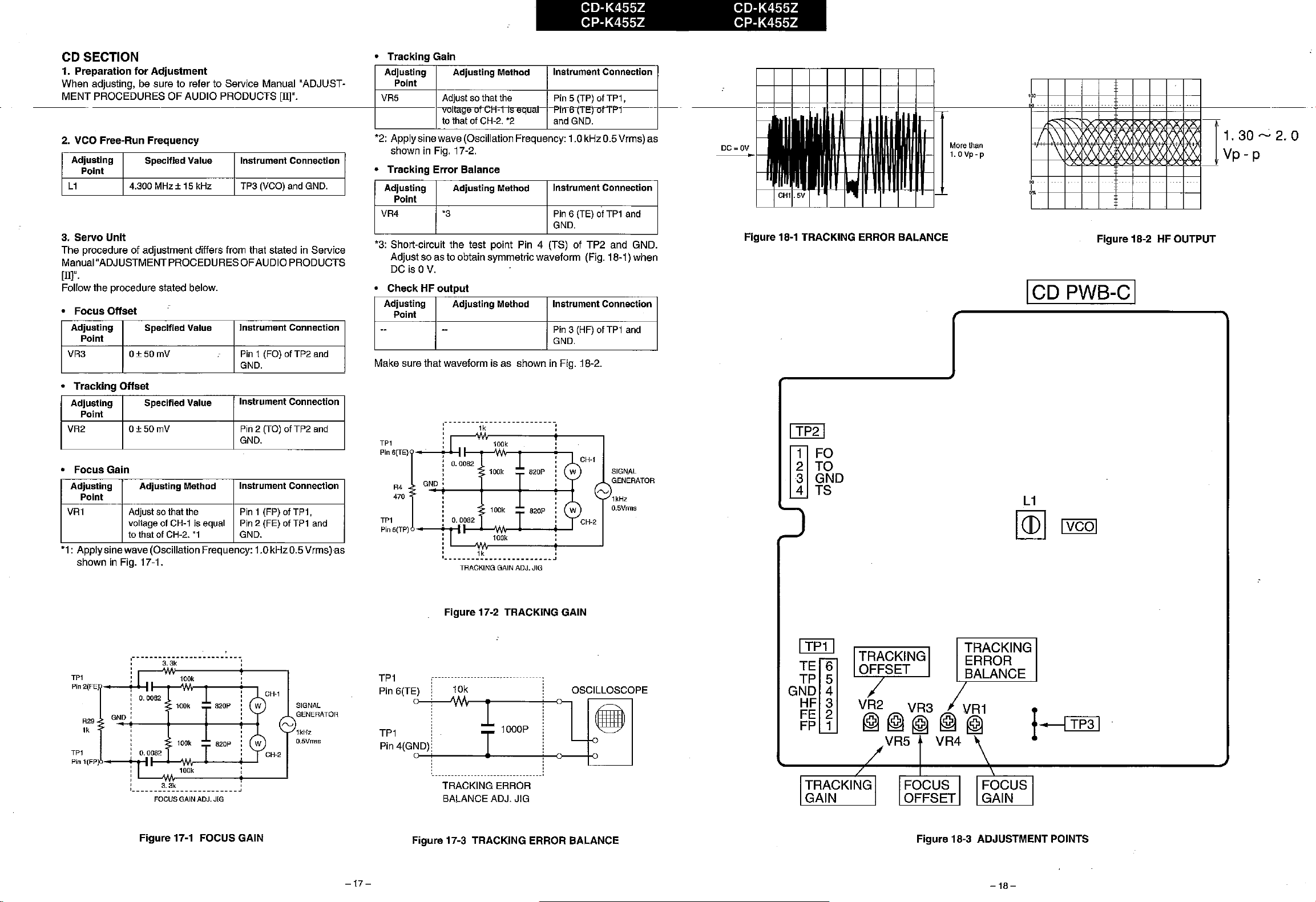
CD SECTION
paration
1. Pre
adjusting, be sure to refer to Service Manual "ADJUST-
When
PROCEDURESOFAUDIO PRODUCTS [Il]".
MENT
2. VCO Free-Run
Adjusting
Point
L1
3.
Servo
The procedure of adjustment differs from that stated in Service
Manual"ADJUSTMENTPROCEDURES OFAUDiOPRODUCTS
[II]"
.
Follow the procedure stated below.
o
Focus
Adjusting
Point
VR3
Unit
Offset
for
Adjustment
Frequency
Specified Value Instrument Connection
4.300
MHz±15
Specified Value
0±50mV
kHz
TP3
(VCO)
and
Instrument Connection
Pin1(FO)
GND.
ofTP2
GND.
and
CD-K455Z CD-K455Z
CP-K455Z CP-K455Z
o
Tracking
Adjusting Adjusting Method
Point
VR5
'2:
Applysinewave (Oscillation Frequency: 1.0 kHz 0.5Vrms) as
shown
o
Tracking
Adjusting Adjusting Method
Point
VR4
'3:
Short-circuit the test point Pin 4 (TS) of TP2 and GND.
Adjust so as to obtain symmetric waveform (Fig. 18-1) when
DC
o
CheckHFoutput
Adjusting
Point
--
Make sure that waveform is as shown in Fig. 18-2.
Gain
Adjustsothat
-vultage-otCH1is·"qoaJto
thatofCH-2.
in
Fig. 17-2.
Error
Balance
'3
is
OV.
Adjusting Method Instrument Connection
--
the
Instrument Connection
Pin5(TP)ofTP1,
-PiIT6tfE)-orTP1---
'2
and
GND.
Instrument Connection
Pin6(TE)
GND.
Pin3(HF)
GND.
ofTP1
ofTP1
and
and
'r----j-+-+-+-f-+-+----j-+--i
-
-[
DC=QV
•
Figure
18-1 TRACKING ERROR
BALANCE
More
1.
than
QVp-p
H-~~~~~~
Figure
18-2HFOUTPUT
1. 30~2. 0
Vp - p
ICD PWB-ci
o
Tracking
Adjusting Specified Value
Point
VR2
• Focus Gain
Adjusting Adjusting Method
Point
VRl
.
1: Applysinewave (OsCilialion Frequency: 1.0kHz0.5
shown in Fig. 17-1.
TP1
Pin2(FE~
R29
1k
TP1
Pin 1(FP
Offset
O±50mV
Adjustsothat
voltage of
to
thatofCH-2.
~-----------------------~
:
__
-i,""'"
0.0082
GND:
0.0082
3.3k
CH-1
100k
100k
100k
the
is equal
'1
Instrument Connection
Pin2(TO)ofTP2
GND.
.
Instrument Connection
Pin1(FP)ofTP1.
Pin2(FE)
GND.
,
~
~-'-00-k_--..,..----'
:
~._3~
FOCUS GAIN ADJ. JIG
~
ofTP1
SIGNAL
GENERATOR
1kHz
0.5Vnns
and
and
Vrms)as
TP1
Pin
6{TEl?--'-+Y
R4
470
TP1
Pin
5(TP)b--.....,
TP1
Pin
6(TE) 10k OSCILLOSCOPE
TP1
Pin
4(GND)
,
0.0082
,
GND:
0.0082
.....
:
,------------------------~
Figure
~---''{1fy-.....,.----+--o-,
100k
lOOk
I--<>--Wv-~----+--'
100k
1k
TRACKING GAIN ADJ. JIG
17-2 TRACKING GAIN
10001"
:
~
o--r----T=>---t=----.J
:_--------------------------------_:
TRACKING ERROR
ADJ.
BALANCE
JIG
SIGNAL
GENERATOR
1kHz
O.5Vnns
I
TP21
FO
2 TO
3 GND
4 TS
rn
I
TP11
TE 6
TP 5
GND 4
HF 3
FE
2
FP 1
TRACKING
GAIN
TRACKING
ERROR
BALANCE
VR2 VR3
VR1
@@@@@
VR5 VR4
Figure
17-1 FOCUS GAIN
-17-
Figure
17-3 TRACKING ERROR
BALANCE
Figure
18-3
ADJUSTMENT
POINTS
-18-
Page 14
CD-K455Z CD-K455Z
+8
FM
SIGNAL
CP-K455Z CP-K455Z
MW/SWl/SW2
SIGNAL
fATN-PWS"TAlTZiJT·-·-·---·-·-·----·-·-·----·-·-·----.-.-.-.---.-.-.-.---.-.-.----·-·-·-·-·---·-------1
A
(
MUTINC
R263
'"
C272
\/50
R299
I.
5K
Q229
25CI.7:40,5R,
50201
ANIENNA. l
TERMINAL
PM
B
,;*::"~
75:
o
hlllfr"y
i
GNDl
@H
-----
~;II@!-
5WZJ_,-.!
1
..
: RP
_>
-,
.
'V
1 IN
AGG
c
C295
1/50
RZ9B
I.
5K
L212
O.
22",H
(
FUNCTiON
"
P22
10-B
D
(
E
R258
m
(
F
G
'V
'V
Q210
ZSC2878
'V
B
._._._._
R231
'OK
•
TC206
,"p
T206
SWl OSC
L....--
__
H
._.
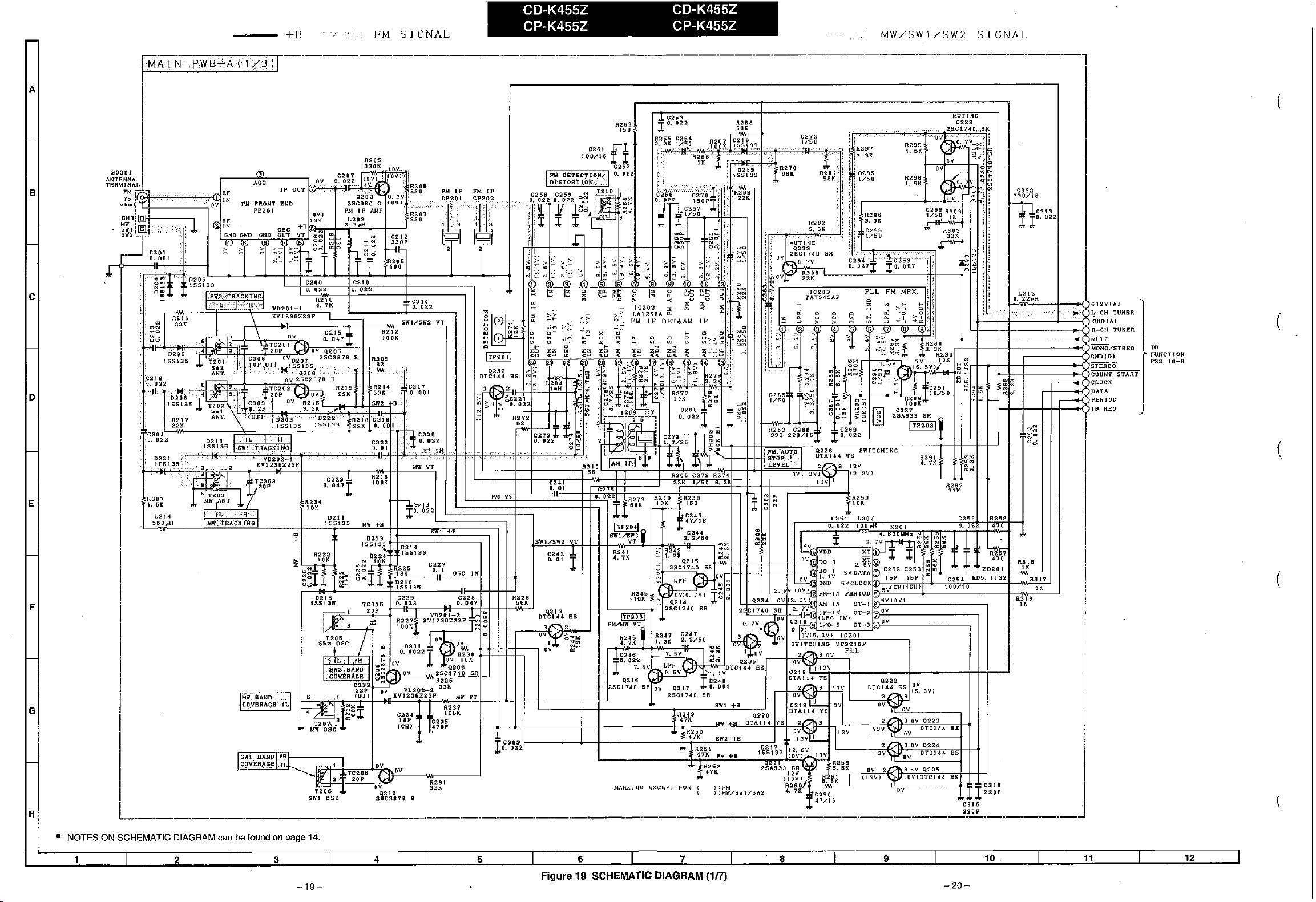
• NOTES ON SCHEMATIC DIAGRAM can be found on page 14.
2
3 4
-19-
5
Figure 19 SCHEMATIC DIAGRAM
6 7 8
(117)
9
-20-
10
11
12
Page 15
CD-K455Z CD-K455Z
CP-K455Z CP-K455Z
-·---f----
I--
I--
-
CD
ill!!Ii!J
~
FM
+B
A
B
C
SIGNAL
-B
~
PLAYBACK
SIGNAL
R621
1K
RECORD
R656
".
SIGNAL
SIGNAL
I I [ I
ffi
g;
z z
, ,
......
a 0
• 0
."
o "
.1
~ ~
~ttt1~~~~~~~;;~13~
l
4700/6..3
C643
a661
".
D608
1S5133
SW201
SPAN
SELECTOR
~IOO/10
L
i
~NS801~
I
SPAN
2--TUNER
4
--
MONO/"
5
CNDWI
6
--
S'fEREO
7
COUNT
START
MUTE
8--CLOCK
9
DATA
--
PERIOD
IF
REO
+5VIBACKUPI
+5VlUN-SW)
P33
I-D
AUX
o
R-CH
I-
E
-
F
~:F'
i'JiI
12-E
-
G
-
t!
f'!
•..
1 IK TAPE 3
'
t!
.
[
FUNCTION
CONTROL
A B
O.
~""
eNS
a
~.IE'~~~~~~~::~~~~~[~~~~~~~~~~~~:~:~~::':R~:~:~~::~:~~::;~~~
r:
t1::.J
- 4
BI601
3
~N~H
00 I
RGll
,~7._K"
__•.__
R632
,,"=_~.
T':i~
~~~~
H H CD
H L
lNPT
TRUTH
TC4052BP
FUNG
TAPE
__
~~_~..
TABLE
(3X,3Yl
(IX.
MOD
IY)
tj
[.'1
Vi
l,
""""""
it~·I~il~~~ff~~~~~~'~--~!'i'I~~':}r~,:m9~;~·l'~e=f·~-~=~O=-~~O=-~=~=~_j_l~~~~~l
'T1"';"..,.;,,~~
'"
,~
'"
R-CH
REC
L-CH
REe
L-CH
P/B
GNOIAl
R-CH
P26
TO
TAPE_
12-E
P/B
+12VCAl
+12VCMl
TAPE
GNOIMl
DUBBING
r-t-l_l~Ftlt----r~~~·~~~~·j·~'~~~~~~~~~~~~~~~~~~~~~t~~t~~~~~~~~~~~~~~~~~~j~j~I~[_POWER
'---.-----\-HH-.---.c.-"+-+-,""
7.7V6
.:ox
13X
:~:::
~~~:~
7.7VIJJ
R522
1"'6
0
a
AUX. 2--S-MUTE
TUNER
"'",
:::~
~
......
:g;;;
~~:;:~
":~:.
R.3DV 4.av14.DaV
I -
I
C6:O
2
~~tg~~~
SELECTOR
R655
'"
~;;;~;n..,
0:_
<aUl
",P>
Q:;-
",Ill
Q.~
,~~:i,
:::IV
Q6:O
IHAI14
J
2(\.
LI}~'~V-----l-------l----+--!jJ.!-+-------J.---J.---l--l--l--+-~
ES
~~I
OV
2 3
",::l
SWITCHING
__
~lO~"~"~l'~"'-i===O=T='~~l~',~'"~y~!~=~'f.'~"=VV±_+_i
Q603
O:A~,"
3
v
DTCI14YSR657
D614
155133
06
I 0
155133
fiG67
22K
~
"~V
~~,~,'-'-r-----,
2.7K}._
RoG
6 5
15K
i
41~'~~~'i,:v~~~~,~~~~~~~~~~~~~;'I~.
I.
:~,.;",
H
I~
!!
~=~=~~~tttttttlt~k=::~'C
",::l
~~
I
R664
lOOK
.'>%'
3.
C645
I
CNS802~
AuX
4--TAPE
5
~
D611
ISS!33
eNSU03
4---
~--:~D2~M/LAMP)
5
--
~:-
8,,------
N
P604
1
:-oMw",TRE
:2
r
TUNER
+5VIUN-SWI
4
5
+17V
6
-17V
8
+12VIMI
9 LAMP
+
@I
GND
1 -GND(D1
3/50
GND
P33\-P
TUNER
CD
~
+12V(A)
P33
1-G
+17V
-11V
~;O'~A1
R-CH
~
CNS604
P29
\-0
+B
(lUI
(M)
-----------_._-------
H
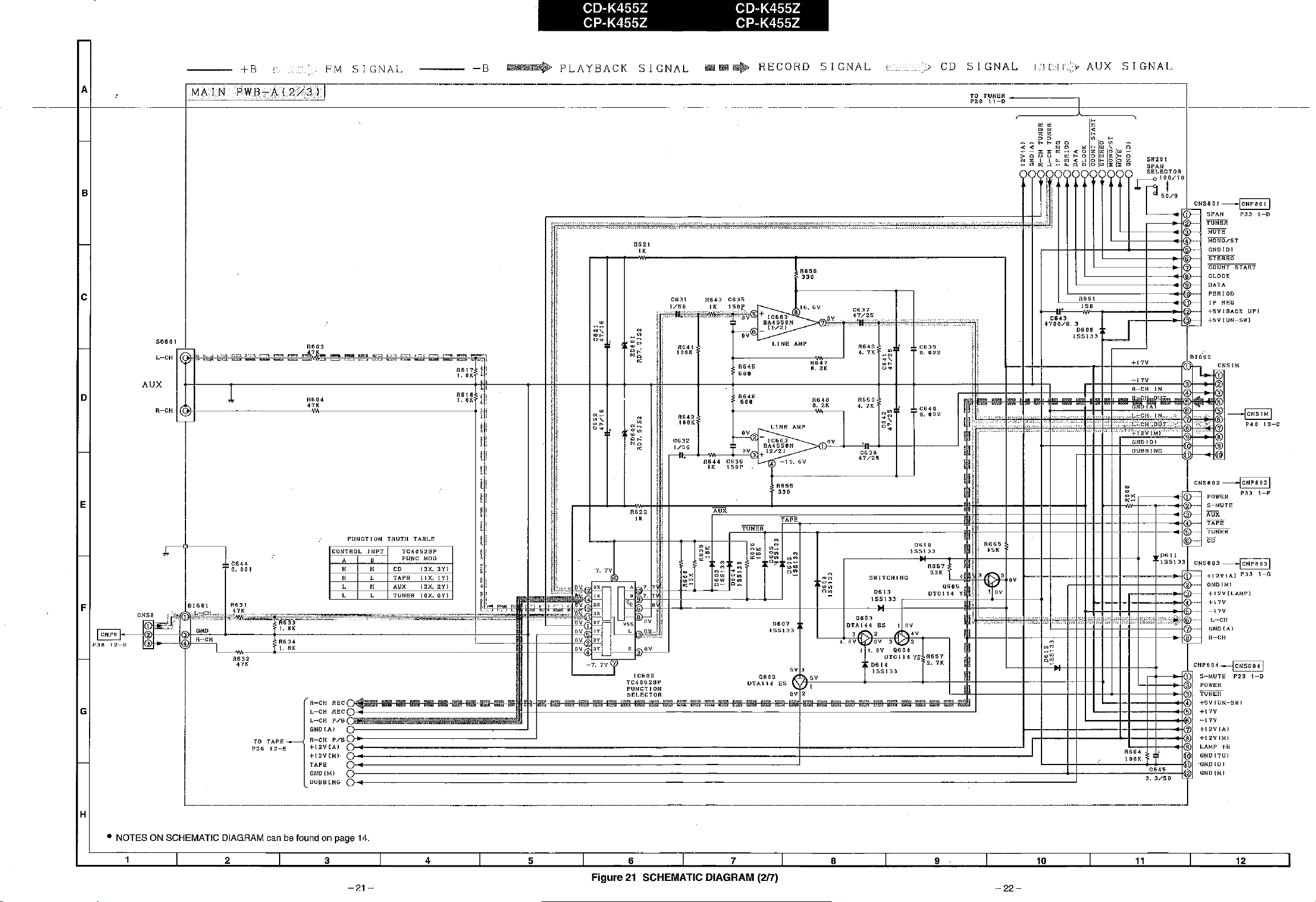
• NOTES ON SCHEMATIC DIAGRAM can be found on page 14.
I 2
I
-------------_._---------_._-_._--_.
-21
T
4 5
I
6 7 8 I 9
Figure21SCHEMATIC DIAGRAM
-
3
(217)
__
._---
------_._---_.
__
._._--_._---_._._--
I
-22-
10
I
11
12
!
Page 16

CD-K455Z CP-K455Z
- 455Z
A
(
COLOR
TABLE
BROWN
""
RDm)
YL
BL
'L
BY
WI-1{W)
B'
p,
RED
ORANGE
YELLOW
-GREEN
BLUE
VlOLET
GRAY
WHITE
BLACK
PINK
---oe-
B
SOL401
T1
APSS
-
[jbl:==,
SW407
~
TI
c
APSS
~~f
~D-
I
TAPE
q
P.B
HEADI69!
OR
CNS405
~lW
ERASE
o
HEAD(71
W
__
~-
)
,
REC.!
P. 8
HEAD
~""
"
170
!
""""
(
BL
SW40Z
TI
0
MOTOR
B"
YL
M401
MOTOR
E
SW406
TZ
RECORD
B""
F
0
SW405 SW403
TZ
MUTINGTZMOTOR
SW404
TI
MUTING
0
0
,
,
"
W
,
,
W
,,
,
,
B
W
CNS403
(
G
H
2
3
54
Figure
23
:IRING
SIDE OF P.W.BOARD (1/5)
-23-
987
-24-
10
11
12
Page 17

CD-K455Z CD-K455Z
CP-K455Z CP-K455Z
W
[j.V
8A3707
IC405
SWUl
i I
APSS
A
B
SOL(OI
TI
APSS
CUSHl
M~~~~
"
(MJ---i,
::
~~;~;::
TI
MUTINe
5'1'05
T2
MUTING
S"'05
72
21111r=~'
sw
SW
/Ille
sw
II
,
~Ii
t--
/1(19
210
lIPSS
•
:;:-
~..
-••Ul:
J
~l
"....
0_
..'" !
~
:=-f~
I-
.~~~1:
~_
-'"
-"'''
----.-
Q(10
liorc,u
ES
ov
5V
112
i 1
~3
DV
/1551
~.5rr----
'"
)'PWBc'AI3/3
/l569
'"
---~-------I
\I
I
c
SWITCHING
o
l.-eH
_
ITAPEIIP.II
E
F
G
IIEAD
/I-eli
_
+B
PLAYBACK
SIGNAL
RECORD
SIGNAL
APSS
SIGNAL
~
;~tr
C(86
'.7/25
TO
PU'lCTlON
P21
/1460
2.7K
/1550
U
85(S
"
/1549
"
0430
155119
..
3-G
H
• NOTES ON SCHEMATIC DIAGRAM can be found on page14.
123
-25-
BIAS
OSC
C4BB
100/16
4
51'1401
B':':':';';;';'A1U59
'rr'
BEAT
CANCEL
"
•
5
.
6 7
Figure25SCHEMATIC DIAGRAM
~_~
__
~ ~
(3")
8 9
+5
J
10
11
12
-26-
Page 18

-K455Z CD-K455Z
CP-K455Z CP-K455Z
A
AC 11OV/127Vj
220V
/230-2411V
J
CORO
50/6OHz
N-r","~""'
R ,
~.:
,
,
CNS702
AC
POWER
SUPPLY
(110
B
c
,
'L
,
"
YL
4
OR
,
RO
,
OR
,
CNS902
(
D
E
PHONES
F
CNS903
RO
OR
YL
OR
,
RO
,
OR
,
YL
•
,
"
,
'L
VL
7
•
WR
,
OK
'0
"
"
'L
"
CNS604
(
(
I
il
I I
I
I
G
~I
,--
-~
( )
L L
H
I'
I I
-.JI
J
COLOR BR
TA8LE
BROWN
RD(Rl
RED
OR
ORANGE YELLOW
YL
OR
GREEN
BL
BLUE
VL
VIOLET
GY
GRAY
WH(W)
WHITE
BK
BLACK
PK
PINK
1
2
3 4
-27-
5
Figure 27 WIRING SIDE OF P.W.BOARD
6 7
(215)
8 9
10
-28-
11
12
Page 19

CD-K455Z CD-K455Z
CP-K455Z CP-K455Z
+8
FM
SIGNAL
-8
A
B
MUTING
c
Bigoa
5-MUTB
poweR
TUNER
•
+~Vllln
SWl
...
17V
'"
+12VIAl
+UVIHI
l.AMP
+a
D
GNDlTUl
GNDWI
GKO(MI
~
E
F
I
a906
0902
•.
7/~O
"
R920
0919
",
",
R942
09lo
1/50
;§~~~~"'~~~~··"H·
5.IVI:lV
0972
O.
022
0900
47/25
R994
~
0912
2S1l175~
av
11989
Q9lS
2S02~61
G975
22
....
ISV
",
",
IlV\irfj20V
lJ.!iV
0975
U/25
50
Q920
25D468
C
R990
PJ
5.
7V
"
11.991
f-m
'"
VOLTAGE
REGULATOR
Q917
2902061
P
Q91
S
2SC17H
SR
RS87
."
RDI3152
REGULATOR
Q91e
IlTA1U
R988
20965
13.5V
R908l:~"
220
14V
C9H
10/50
VOLTAGE
...
------.-.---
,-
1
q915
OTAI U I!S
I
20V
2
R994
:v
SVA:"'lo.DV
9 2
,
':fv
Q9U
IlTelUY5
lK
J
20V
/1.985
tOK
liS
~T-,-H",A",N",.,,-S
1199.1
1190.1
Ill-IOU
-,,-PW=8
8.2K
0959
'n;~o
~
~~~~
3
0::'162
5600/63
+
0960
o.
022
L
__
h h
..
--+-~~~·b~'''-'''''-'"''--------·----·----------·-J
,,-,,-8::c.J2
11912
-
54V1I20
~
IT
.I""i'
~
I
CKS902
"""
C982
0.22
IMI.)
CUl
0.22
IMLI
1:958
10/50
I--~"'--l
-lOY
*.,.,tt.'9-,=.-'"'.'J,:"~...j
_17.
"v
nvl
Q907
,.~
259562CR958
~.9n
...
1.2K
~gmS:l
Z0902
RD16JS3
R969
3.
9)(
IPOWER
G
H
• NOTESONSCHEMATIC DIAGRAM can be found on page 14.
1
2 3 4 5 6 7 8 9
-29-
Figure
29 SCHEMATIC DIAGRAM
(4m
-30-
10
11
12
Page 20

CD-K455Z CD-K455Z
CP-K455Z CP-K455Z
t
;"'-
(',
~-~i_:-'~
-
A
i~-~
,
·i_~
RD
BK
(
\
B
c
D
CNS601
P24
rr-H
COLOR
BR
RD{R)
OR
YL
GR
BL
VL
GY
WH(W)
BK
PK
TABLE
BROWN
RED
ORANGE
YELLOW
GREEN
BLUE
VIOLET
GRAY
WHITE
BLACK
PINK
(
(
E
I
YQ~UME
F
G
H
2 3
4
-31-
5
Figure31WIRING SIDE OF P.W.BOARD (3/5)
6 7 8
9
-32-
10
PWS-021
11
12
Page 21

CD-K455Z CD-K455Z
CP-K455Z CP-K455Z
FM
SIGNAL
----6
LOD80ITUNER/CD
LCD
----I__'L~C::'O"___'P__'W__'B"__~__'O"__l'__l
A
I
R810
ov
OV
"
,.
"
"
C801
!IOOU.10
C802
0.022
0801
155133
SWBD2
rif-.',f-,-,
~+--f---(:O~1l
155133
DB01
RBJH
"""'
I
~~~~~
~
'.
,.
~."~~pH)---'
155133
DBDa
lSSln
C807
":,~.
10/50
5V
SInD
BAllO
."
"
SWBOS
.,~
.~~
I
C80e
330P
_0O!"
,,<'>
....
::::::,"111
SEGl2
SBOIS
SBGH
SeGIS
seCle
B
seOl7
SOllia
SEGIS
BOOZD
SEG21
S8022
58023
SI!G24
SBCZS
SEG26
sec,,?
I
CBO'
RH-IXI846AF
TUNER
CONTROL
MI
CROCOMPUTER
~I~~~
-
~.
~
8
MONO/STBIiIlO
."
IP
Rill!
MUT8
c
P22
12_B
CNSBO I
D
--®
cnpso
•
I
SPAti
TunER
MUTE
MONO/ST
cnOIDl
STEREO
counT
CLOCK
DATA
PERIOD
IF
REO
+5VlBACK
+5V(UN_S'i")
START
UI'I
C810
0.01
CUI
D.
Dl
C813
0.01
R815
R817
"
=:"~~"~===I;r~=-:,'--jfP9i.!,*",.[]."9I-,~-""--j;~"I-;~:"-"1C:~:o!~o_~:ol--+---II~+
~:~~~~~
:~:~~~:~~~:~8gg8
ReSl
1f~==~~'~I~'II"JJ~~~~~~~~~:~~~::~~~~u
'"
,t'
"."'
Down
SW854
R856
>cd
swa53
UP
SW855 SW856
Ra55
10K 10K
m
swa52
O/C)-----++--=
SW851
RS51
10K
0851
lSSIB
....
",-+-'
ISSI33
R858
10K 10K
R859
'"
R860
u
C8s8
ICHI
'"
R869
"
LAMP
.eWB.+O
L.CD
BliCK
I
PLOD
3
LICHT
IL-_~_"~":_'~_":~·_.~"'-<1fi~~·-'~-J'i-I--
llIBOI-A
CBS4
D.
022
CB55
0.01
C856
0.01
C857
'"
lCHi
1S8
RBBB
(1/4)
la51
1 I MUTI!
r-
:f,
4 ---l r
-.II
___
___
8 8 TRAY
___
__
CN55~
TRAY MTR
TRAY MTR
+8V
®t1C
ctlDlDl
PU-IN
TRAYSWOPEti
LANF
lD"
P3B
8-c
OPEN
CLOSE
SW
·SW
CLOSII
E
F
G
H
~:
'"'1"1
PZ212F
CtlS803
TUNER
CU
S1I812
Clf1'802
POWER
S MUTE
,.,
TAPE
TUNER
POWER
SW809 SW811
"
ClfP803
+12V(AI
CNDIMI
+l2YtLAMPI
+17V
'"
L_CH
llNo-(Al
" '"
I
L .
CBI8
47/16
C81S
0.022
RB34
'"
LIlDSOS
3N41101133
STAIID BY
lifO.
LB02
100,Jl
• NOTES ON SCHEMATIC DIAGRAM can be found on page 14.
1
2 3 4 5 6 7
-33-
Figure
33 SCHEMATIC DIAGRAM
(517)
B
9
10
12
"
-34-
Page 22

CD-K455Z CD-K455Z
CP-K455Z CP-K455Z
P24
IO-A
9D
A
P2B
Y
12-E
P31
~
4-E
(
B
SR
RD(R)
OR
YL
GR
BL
VL
GY
WHeW)
SK
PK
TABLE
BROWN
REO
ORANGE
YELLOW
GREEN
BLUE
ViOLET
GRAY
WHITE
BLACK
PINK
(
CNS4
,
,
3
4
•
c
D
P31
5-E
-,
I
CNS3
BR
,
,
OR
3
4
BR
RD
OR
YL
GR
o
DISC
CLOSE
sw,
HOLDER
OPEN
.3
LOADING
MOTOR
COLOR
~
I
\.
SPIN
.,
MOTOR
(
---
E
~6~6
:,j-'---P-'-C-K-U-P-U-N-"--'
I
13081
_J
I
I
I
I
I
I
I
I
I
I
I
_J
11
12
F
CNS2A CNS28
-D~~I~~~D-
G
H
•
The
numbers8toCDare
1
waveform
2 3 4
numbers
showninpage
-.35-
42.
5 6 7
Figure 35 WIRING SIDE OF P.W.BOARD (4/5)
CN5lA
,f-__
...,-,-
--iG[!V_--.
,----U~+=l~
~I=::iR=1
•
f~=lb=::;;tr-----"!:-.J
8
GY
9
-36-
10
eNSIS
4
3
,
(
Page 23

CD-K455Z
'CD-K455Z
CP-K455Z CP-K455Z
A
B
eNSIS
-~B
,
,
"!Q'
CNSIA
" _ 4
c
GNP}
l~
~Il.
,'
hi
,
,
--
.
47/lli
"
I~
RI32
'"
Rt.33
HI30
I.
OK
D
PI
CKUP
PNIT
E
"
CI22
47/16
lj
CN52B
F
+8
.,
LOADING
•
NOTES
MOTOR
ON SCHEMATIC DIAGRAM can be found on page 14,
1
2
J
3 4 5 6 7 8 9
Figure 37 SCHEMATIC DIAGRAM
-37-
(617)
G
H
~
PH
12-C
-8
SIGNAL
•
The
numbers 0 to
-38-
G)
are waveform numbers showninpage42.
10
11
12
Page 24

CD-K455Z CD-K455Z
CP-K455Z CP-K455Z
+B
-i
-.-----------------------------------------------------------------------------------------------LECR0
A
I 0
I
II
I
B
C
D
E
I
4-++f-;':;'~K~+r;?~f+;-,
~+~Wr-+-r-<U/
~~~M
C51M
O.
(147
C57M
56~_P_,,_,
C59M
__
56(l_;"T"
~~~M
R52M
68K
68K
C60M
C58M
560P
560P
R58M
,,,
R75M
:27;M
R77M
22K
FM
R54M
C52M
O.
047
IC50M
:'~.""C4~714}'2"t-E~.;·61:·f~"''BrS°.;~j6~07.;IM.:8;4+'lb++2~_@[;:_,8'A
R711M
22K
C65M
tOOP
SIGNAL
~52:';0
"V
R!~8~M
B·
R6IM
5.6K
ov
C56M R68M
0.22/50
ov
7
R62M
5.
6K
I
OV
R79M
'"
MIC
AMP
F'
~i
R65f,f'/
,2?J<;,)
R67M'
27K
27K
R64M
2"
R66M
22K
-B
IC50M.
W1lW1l$'
IC5IM:OPE
~~;{M
R81M
6.
BK
C15
1
:rt.
~4'i-'..c-P":
-8.
GV
RECORD
AMP.
JC51M
B.14741
C"M
~~~M ~~~~
R72M
,,,
C64M
-8.5V
10/50
R74M
1 0 OK
SIGNAL
ANALOG
SWITCH
lC53M
LC4966
7
-B.GY
4-
B';:2M
SWITCHING
D
CIQ1541MyS
DT~5121~
-6.]~3~v
47K
-8.5V
la.6V
MI
C
SIGNAL
-
PWB-F
1
I
(
I
R-CH
IN
BUFFER
R2'29KM
~.,'
~"
D~""
j,
~
AMP.
'.
!
f"
fj
ES
;;;;;; j
tOo
a:~
SW50M
-1
Ie
R9o~.;I:
22K~_,
::>:
~:.:
~~f
,i
~
'''''
1n::N
-j5V
Q5'OM I
DTC114-YS
ov
:73M
47/16
fig 3M:'
4.
7~
15V
g;~6
<I>-..,""=-,-....
Ii*.
R94M;
........
~~4.7K
<:&'''>..''':j!
~
,~
S:J
II
I
I.
I
I'
(
~
~
t'-
•
~
~
_~:~;~:51:~:~~4:':::::J::::l:!:~O~C;7";~~~:~~:W~~~:~~~~:~~~~~~~~~~~::~-:1~::::'::!\11F~~!:r':-j-f-:-{:-~-:-:-:-----:<I--:--"i~~·I-
1
~.
tj~=
f
MIG/BUFFER
AMP.
IC2M
!l~
BA4558N
i;;;;3
-J~;:;
-I
SV
1
'>V
'~;:-+-_++--==~
Rl8M
,
IJ<
'Cd"M"
1
0/50
VR3M
20Kl8J
DIGITAL
ECHO
R~:M
Rl9M
...
JOK
RB4M
1K
t"
u
...
U 0
u...
..
~~~~~~~~~~~~~Hr
R21M
,,,,,~j :"'=~-;
Q4M
DTA114
SWITCH1NG
ES
C14M
~~,:~O;f~!q
5
R25M
22K
C15M
33/10
L-i
H
l1 6
ml, 3
lib~
;[;;;ll!~:l!il~!~]!~~~~l;ll~l~:
~!
,---t--------t_-t_---t<~9)1
.....
~~~~~~~~+~_t~~-.__H])1
R27M
C46M
O.
022
C44M
47/25
C45M
O.
C43M
47/25
" "
022
C16M
lOOP
-11~_t~t_~~~+_+_+~
It
R26M
10K
~
~"l
R28M
""
R-CH
IN
"':
:~~7A~UT
~~
L-CH
L-CH
+12V1MJ
GND
ID I
DUBB I
IN
OUT
NG
P22
7
8
CNSIM
12-D
(
6
~
" =
DIGITAL
ECHO
z z z "
C47M
47/16
._._.
8
LIM
VOLTAGE
REGULATOR
Q5M
2SC200
I L
5.
5V!-cc"WIo-.
~~
R49M
'<1'0
+ 1
00
""
SWlM-A
C
rO
z
0 0
R4BM
dr-
1.
2K
9 10
SELECTOR
---
NORMAL
TAPE
(
CNP804
HI
+B
REC
+8
SWIM-B
H1GH
~
NORMAL
DUB8lNG
SPEED
0
-----------
11
I
2
3
4
6
I
CNS8041
P26
F
"
I
(
12
R7M
tOOK
elM
R'M
_________
J
JIM
MI
C
F
.'
G
H
• NOTES ON SCHEMATIC DIAGRAM can be found on page 14.
___________________________________________________
L
[II
r---------~
___
;;_~
MICm
J
4.
R4M
4.7K
i
L2-iT-f,C..,."Hli2""',.,'S:~'P,oS,y~-·
2 3 4
lOOP
7K
C2M
lOOP
R8M
lOOK
k"~G~
:"-'-'Rff'""'~t:160~'~1sv~:
C9"
t/50
C10M
1/50
RlOM
"'0
t-"R
OC
':"-----,
12:CM
120K
~~~p
'V
~51;:<""
VR2M
20K
{Sl
MI
C
[II
LEV
EL
~,:")t'"1,M"6?;'Jif"
!',
,:,4-7K
Cl2M
l'
7<:https://manualmachine.com/~;,--
J
;~~4M
R34M
15K
?;.~
• •
5 6 7
~
U
C34M
O.
,
c
022
XIM
4.
05MHz
C25M
0.0033
R40M
~~
\CJ54~
N
RJ9M
o
R33M
U
2.7K
10K
R4tM
10K
I
C2
0.012
CIOM
0,022
ICJM
R42M
'"
8M
N
N
..
M50197P
~~
Uo
2 3 4 5
C30M C31M
o 01 0 1
o~
Figure 39 SCHEMATIC DIAGRAM (7fT)
-39-
-40-
Page 25

.--A1-------
B
c
VR3M
DIGITAL
ECHO
CD-K455Z
CP-K455Z
o
E
VRIM
F
KARAOKE
MAKER
G
H
2 3 4
5
6
Figure41WIRING SIDE OF P.W.BOARD (5/5)
-41-
Page 26

CD-K455Z
CP-K455Z
HF
o
O.
O.5psec/Dlv(DC)
(When
FRF
O.5V/Dlv
SOm
FE
O.
SQm
STOP--PLAYBACK
tV/Dlv
back
sec/Dlv(DC)
tV/Dlv
sec/Dlv(DC)
p]aylnS
the
disc
WAVEFORMS
II":
0:
l'.'
rg
/
,,\
I
~
I
~
II,
I
W'
I
OF
CD CIRCUIT
FRF
O.5V/Dlv
0.5
sec/D
TRACKING
O.
LV/Dlv
O.5sec/Dlv(OC)
STOP-PLAYBACK
~DATA
."
O.
2V/D
O.
Sp.sllc/Dlv
{When
back
J v
I v
playing
the
(DCI
COIL
discI
*.,
r I
....
I'
(
(
1
FDQ
O.
2V/D
O.
STOP---PLAYBACK
FRF
O.5V/Dlv
O.5sQc/Dlv(DC}
FOCUS
O.
O.
STOP
J v
S",sec/Dlv(DC)
COIL
tV/Dlv
SSGe/DlvIDe)
-PLAYBACK
I
I
II
I
J.
IJ
,j,
.'"
1\
~
Audio
Signal
O.2V/Dlv
O.2m
(''{hen
NOTE:
1.
2.
back
Us
8
Output
sec/Dlv(AC}
playing
the
10:1
e
.•.
dJ
se)
11kHz
probe
to
e.0.8
osclIloscope
~
connect.
Th.
for
~
10..
~
PLAYBACK
Sine
wave
"".,.
measurement.
waS
~
10..
discI
uSed
~
(
(
-42-
Page 27

TROUBLESHOOTING (CD SECTION)·
- 55
CP-K455Z
When the
WhentheCDsectiondoesnotoperateWhen the objective lens oftheopticalpickupisdirty,thissection maynotoperate.Clean the objective
lens,and check the playback operation.When this section does not operate even after the above stepistaken,checkthe following items. u
Remove the cabinet and follow the troubleshooting instructions.
Turn the power switchonthe unit to
Does
CD
does not function
ON.
the LCD or fluorescent character display tubegoon?
'I
Check
the
I
No
does
not
go on."
itemof"The
LCDorfluorescent
character
display
tube
1Yes
Does
the disc tray open?
Does
the disc tray close?
Does the spin
When the discisinitialized, is TOe
Is
TOe
Is there
'-
motor
run?
set to the playback mode?
any
audio output?
~
Yes
~
Yes
~
Yes
---.c-c-
~
Yes
read?
---'I
I
No
I
No
I
No
No
No
Check the item of "The disc tray does not open."
"I
Check the itemof''The disc tray does not close,"
"I
Check the item of ''The spin motor does not run."
"I
Check the item of''The disc does not playback."
Check the audio circuit.
I
I
I
I
I
I
I
OK
I
Turn the
Check
Is the oscillating circuit (X851)ofthe control microcomputer
(ICB51)
Checktosee
(IC851) is operating normally.
[s
tube being output from the control microcomputer (IC851)?
Check
display tube,
power
switchtoON.
the
power
circuit voltage.
operating
the
drive signalofthe
the supply voltageofthe LCDorfluorescent character
normally?
Yes
that the reset circuitofthe control microcomputer
Normal
LCDorfluorescent character display
Yes
No
Check the X851 and peripheral circuits
Check
the reset circuit (085,1) and peripheral circuits and replace
faulty
parts.
The microcomputer (IC851) is defective. Replace it.
The LCD
Replace it.
or
fluorescent character display tube is defective,
and
replace faulty parts.
Are
the
connector
Normal
and
PWB pattern damaged?
-43-
Page 28

CD-K455Z
CP-K455Z
lis
the
open/close
key
signal
being
output?
1Ves
liS
the
tray
close
of
the
control
115
the motor drive output being output from pins 13 and 14 of the I
control
microcomputer
1'5
the motordrive output being output from pins 2 and 7
of
the
motor
detection
microcomputer
driver
IThe loading motor (M3) is defective. Replace
The
loading
mechanismisfaulty.
switch
signal
(l)
being
(IC851)?
~
Yes
(IC851)? I
~
Ves
(Ie?)?
~
Yes
inputtopin
it.
18
The
"I
. I
IIC7
openfcl0S:8
Replace
The
control
Is
there
is defective.
Replace
I
No
No
I
No
No
I
I
switchisdefective.
the
tray
close
detection
microcomputer
+8Vatpins1and8of
Ves
it.
(IC851)isdefective.
II
Check to seeifthe
power
Replace
switch.
Ie??
supplyisdamaged.
it.
Replace
No
pwEi
pattern
(
1
I
it.
to
I
I
the I
(
lis
the
open/close
115
the tray open detection switch signal (L) being input to pin 19
of
the
control
115
the motor drive output being outputfrom pins 13 and 14 of the I
control
microcomputer
115
the motor drive output being output from pins 2 and 7
of the motor driver (IC7)?
key
signal
microcomputer
(IC851)?
being
output?
Ves
(IC851)?
~
Yes
t
Yes
Ves Ves
IThe loading motor (M3) is defective. Replace it.
The
.loading
mechanismisfaulty.
Checkthe output of pins 86 (MCON+) and 87 (MCON-)
oflC2.
I
I
No
No
I
No
I
No
I
I
Defective.I
(no output)
~:
The
open/close
. I Replace
The
;:Isthere
IIC?isdefective.
Replace
IC2
the
control
+8Vatpins1and8of
it.
· d
f'
[seectlve.
switchisdefective.
tray
open
detection
microcomputer
II
I'
Rep
ace
Replace
switch.
(IC851)isdefective.
IC??
Checktoseeifthe
power
supplyisdamaged.
It.
it.
Replace
No
PWB
it.
patterntothe
I
(
I
I
(
I
I
I
~
,-------------"-----~-----.,
Check
the
outputofpin2of
Spin
motorM2is
defective.
Normal
1C6.
.L.
Normal
Replace
it.
I Defective
I
-44-
,-------------------------.,1
IC6isdefective.
Replace
it.
(
Page 29

-
CP-K455Z
lis
.!he
disc initialized?
Yes
I
Does
the tracking servo operate normally?
Is
the
EFM
signalofpin36of ICI flat? (Lower side)
Yes
IIs
the
tracking error signal (pin 2oflC1) being output?
Yes
Normal
--
- I Does the laser diodegoon?
No
A Checkthe
....
....
B Check the
if
No
Check
r
Does
Check the waveform of pins 86
(MCON+)
Replace
No
.'
Is the tracking signal being output
from the pickup main unit?
the
pickup
is
Ifitis
dirty, clean it.
the spin motor
Is
there any dropout partinthe
ICP
the
itemof''The laser diode goes on."
item
of ''The laser diode does not.go on."
objective lens of the
dirty.
run
normally?
and87(MCON-)ofIC2.
Normal
EFM
~
Yes
disc or change the program.
No
signalofpin36of
No
"I
Yes
Replace the ICI.
IC2is
defective.
Replace it.
The pickup
defective.
is
lIn
the stop mode, is
CNP2) 0 ±50mV?
the
tracking coil drive output (pin 4 of
1Ves
rIs the tracking coil drive output being output from the tracking
driver output (pin 2ofIC5)?
ves
1
IThe pickup connecting connector is broken.
The pickup tracking coil is broken.
No
r
No
r
Incorrect adjustment
In
the stop mode, adjust the tracking offset to 0 ± 50mV.
IC5 is defective.
The PWB negative pattern is damaged.
I
-45-
Page 30

CD-K455Z
CP-K455Z
When
the
without
pickup
Are
the focus driver (IC5) +8V and
-8V,
Is
for
IC2 being output?
trayisclosed
loading
lens
moveupand
the
voltagesatpins-10
respectively?
the
highllow
leading
the
disc,
does
No
No
Ves
level
repetition
focus
selVaofpin73of
"I
No
Ves
the
down?
and5of
_I
Check
circuit.
[C2isdefective.
the
output
power
Ves
Is the EFM signal of pin 36 of
being
output?
Is
the
FRF
disc
pin75of
(IC2) at a high level?
the
reflection
servo
I
[s
the
outputofpin31of
below?
Pin75of
IC2
FRF
Pin31of
IC1
FE
I
Ves
signal
Ves
IC1asshown
Ves
IC1
signal
control
•
Pickup
height
No
"I
•
Laser
I
The
pickupisdefective.
of
No
The servo amplifier (IC1) is
~
1
defective.
diode
error
output
error
Replace
it.
(
I
I
I
(
~
I
The
selVa
No
defective.
amplifier
(IC1)
is
I
(
Is
the
high/low
output
Check connectors CNS2A1B and
from
repetition
pinBof
output
IC5?
Ves
,
being
CNP2.!
No
Checktosee
distribution
The
focus
driver
that
the
connector.
focus
(IC5)isdefective.
circuitisnormal
Replace
and
it.
check
the
I
I
(
-46-
Page 31

~
~1&1baJasBLCOIllroLsignaLaLIlin-9-(1
(IC851) at a low level?
Ves
ANE)
of the
microcomp~
No
Is
the06laser
emitter
voltage
diode
driver
+5V?----
Ves
-
CP-K455Z
Check
the
clrcUJ
.
power
Is
the
pickup
Is
the
Check if pins 84 (EEM+) and
outputting.
Check
'-------_---,------'-------------'
Check if there is voltage at CNP3, Bi3/CNS3 and
lis
there
I
Is
there
returnedtothe
pickupinswitch
pin8of
the
slide
aUdio
output?
aUdio
output
SW1
motor
l
from
innermost
turnedtoON?
Ves
85
(EEM-) of IC2 are
Normal
driver
Normal
No
both
Land R
Ves
part?
(ICB).
channels?
M1.
IC2
Defective
I--~---I>I
Defective
is
The
I
.
I
No
• Check
• Check sound coupling capacitors
Cl02,
defective.
slide
motor
the
Cl10
Ves
Replace
driver
muting
(R-CH).
it.
(ICB)isdefective.
Transistor,
Q103
Replace
and
Q104
Cl01,
ClOg (L-CH) and
SW1isdefective.
Replace
it.
it.
and
replace.
liS
there + 7.3V at
lis
pin15of
115
pin3of
Je85i
0103
IC101
muting
and
and
1Yes
output
Ves
0104ata
Ves
I
OK
ICl
I
02?
atahigh
[ow
level?
level?
~I
Check
power
circuits
0912
and
and
0913.
0107
and replace faulty
I
No
I
I
No
No
-47-
.1
Replace IC851.
Check the voltageof0106
parts.
Page 32

- 55
CP-K455Z
IC2 VHiLR376321-1 (LR37632)
FUNCTION TABLE OF IC
PinNa. Terminal
Name
1 LOIN Output
2'
3'
4
5'
6'
7'
8·15
16 VDD
17, 18,
19
20
21
22-29
30
31,32
33 04
34'
35
36'
37
38'
39'
40
41
42
43 2C/OB Output Setting of
44'·59'
In
FCON Output
MUTE
SBCL
SCREQ Output Sub code take
SDATA Output
SSYN
AO-A7
~A9
WE
OE
A10
D8-
Dl
DEPH
XIN,XOUT Crystal oscillation terminal
02
SDO Output
SDSY Output
882K
SWL Output
SWR Output
GND
LROR
TIN Input Digital filtering ON/OFF switching
DA1·
DA16
this
unit,
the
terminal with
Input!
. Output
Free_running
sync signal coincidence output
Laser output ON/OFF timing
control
Output Frame asynchronous output
Input
Sub code call clock
Sub code
Output Subcode
Output Address signal, data signal and
-
Output Address signal, data signal and
Output Address signal,
Output Address signal, data signal and
Output Address signal, data signal and
Output
-
-
Output Synchronising signal output
Output
input control signal
Power terminal
input control signal
input control signal
input control signal
input control signal
Deemphasis control signal
Synchronising signal output
1/2 sync signal output
Synchronising signal output
UR
channel sync signal output
Synchronising signal output
Deglitch SWL output
Deglitch SWR output
Earth
input
music signal
16-bit source signal parallel output
asterisked
Function
syn"c
signal/Frame
in
completion
data
output
sync
signal detect flag
data
signal and
data
formatof16-bit
mark
nIs (open) terminal
Pin
No.
60"-62"
63
64'
65'
66
67,68
69
70'
71",72"
73
74
75
76
77 TER
78
79
80
81,82
83
84,85
86,87
88
89
90
91,92
93
94
95
96
97
98
99
100
whichisnot
Terminal
Name
TINl
-
TIN3
0S
DFCL
CRCC
VDD
TESTl-2
C1FL
DFL
C1F,C2F Output Error state output
FCS
FZC
FRF
HF
TRO
TRGL Output Tracking servo gain SWitching
TRHD Output
KP+,
KP
FEOF
FEM+,
MCON+,FD
PD
GND
VCO,VCO Input Clock oscillation
EFMO
EFMN Inpull Auto-level slice
EFMI
WQ
RIW
DOUT Output
DIN
'SCI<
connectedtothe
Input!
Output
-
Output
Output VCOframe sync signal
Output Sub
-
-
-
-
Output Focus servo initial writing signal
Input Focus point indicating signal
Input Disk reflected signal
Input HF envelope signal
Input Tracking error signal
Output Tracking servo operating area
Output Kick pulse signal to move pickup
Outpui Tracking errorsignal stop
Output Field pulse signal to move pickup
Output Spinservo control signal
Output VCO
Output Phasecomparator output
Output Auto-level slice
Output
Input Auto"level slice
Output
Input
Input Command data input
Input
Test terminal
System
Powerterminal
Test terminal
Test terminal
Test terminal
switching signal
signal
Tracking error signal level hold
signal
Earth
Q code output
Q code input
Code output
Clock input
outside.
Function
clock standard output
CRCC
error detecting output
dock
error output
(
(
(
(
-48-
(
Page 33

-
CP-K455Z
IC2 VHiLR376321-1 (LR37632)
KP+
KP-
FEOF
FEM+ 8
FEM-
MCON+
MCON-
FD
PD
GND
VCO
VCO
EFMO 9
EFMN
EFMI 9
WQ
R/W
DOU
DIN
SCK 0
B1
8
8
8
8
8
8
8
9
91
9
9
9
9
9
9
8079787
123
z z
-o=>
OUO
--1LL~
787574737271706988678885848362618059585
456
I-
--'0<
UWI-
ffiOC<
Ol
U 0
OlOl
~
N~
Uoo~~~~oom·ouu
NUN~~-WWo~~m--~~~~~~<~~<
~~UUDUrr>UO~rrrOOOOpOOOO
~~r
O~
LR37632
CTOP VI
7 8
910111213141518171819
EWl
mN~m~~mN~O
ZZZ~~_~~~_rnro
565554535251
0 1 2 3 4 5 8 7 8 9 0
J-'87i---{2
3B)---{,3
SDSY
OEPH
4
T/N
Figure 49 BLOCK DIAGRAM OF IC
FCON
MUTE
r-c-=J...,..=-,
MUTE GEN. E
CLOCK GEN. &
TIMING
OUT
3)-----,
GEN.
T
S
T
p
I
N
;2
,4
H--IS~XOUT
31
XIN
41
LROR
3
882K
4
DA1
(
DA18
-49-
Page 34

CD-K455Z
CP-K455Z
IC4 VHiLC9600AM·1 (LC9600AM)
PinNa.
1
2
3'
4
5
6
7
8
9
10
11'
12
13
14
15
16
17
18'
19'
20
In
Ih,s unll, the terminal with aslensked mark n
Terminal
CH10UT
VrefHl
VrefH2
VDD
WCLK2
LRCK
WCLK1
DATA
BCLK
VDD
TSTOUT
TST1
TST2
IF
GND
VrefL1
GND
VrefL2
NC
CH20UT
Name
Inpul/Oulpul
Output
Input Reference voltage "H" input terminal 1
Input Reference voltage "H" input terminal 2
Input
Input
Input
Input
Input
Input
Input
Output
Input Test output terminal
Input
Input
-
Input
-
Input
-
Output
Function
CH1
output terminal
Power voltage
Word clock 2 input terminal
When
LR
clock input terminal
Word
clock input terminal
When
IF="H"
Digital audio data input
When
Bit
clock terminal
PWMDAC
Power
Test output terminal
Ordinarily it is·open.
Ordinarily it is connected GND.
Test
output terminal
Ordinarily it is connected GND.
Interiace switching terminal
MBB
first: When digital audio data input format
LBB first: When digital audio data input format is
GND
terminal
Reference voltage "L" input terminal 1
GND
terminal
Reference voltage "L" input terminal 2
CH2 output terminal
IS
(open) terminal whichISnot connected to the outside.
term
IF
=
"H"
levelisset
levelisset
IF
= "H" level is set
clock
and
voltage
term
inal
+5V
terminal
clocktoread the digital audio
inal+5V
dala
is·
at
at
IF="L" level
into LSI as bit serial
IF
="H" level
data
(
IC4 VHiLC9600AM-1 (LC9600AM)
f0-
il
(5
r--------{1
-N
II
~
• •
»
" "
~
CH10UT
VrefH1
VrefH2
VDO
WCLK2
LACK
WCLK1
DATA
BCLK
VDD
"-J
1
20
2 19
3 18
4 17
5
6
16
15
7 14
8 13
9
10
12
11
CH2QUT
NC
VrefL2
GND
VrefL
GND
IF
TST2
TSTl
TSTOUT
1
(
Figure50BLOCK
-50-
DIAGRAM OF IC
Page 35

IC803 92LiCiX2031 (IX2031)
Pin No.
7
Terminal
Name
1
2
3
4
5
6
K3
VOO
CK
ROY
SOO
RMC
CO
8 TUNER
9
10
11
12
TAPE
PHONO
AUX
S-MUTE
13 POWER PA2
14'
15
16
S·R
XOUT
X1N
17 TEST TEST
18
19
Vss
RES RES
20 V-UP
21
22'
V-OWN
FLAS PC2
23 X-BASS PC3 Output X-BASS control output
24'
25
FO
Fl
26 F2
this
unit,
F3
KO
Kl
K2
the
27
28'
29
30
In
Signal
Name
J;>E3-VOO
SI
SO
SCK Output
InputlOutput
~utpUl--
-
Input
Key_matri"-'-Outpu
Connect to the power supply (+5V)
Remote
control clock input
Output Remote control ready output
Remote control data output
INT Input Remote control input
PGO
PGl
PG2
PG3
PAO
PAl
Output
Output Function control output
Output Function control output
.Output
Output Function control output
Output System muting output
Function control output
Function control output
Output POWER ON/OFF output
PA3
Output Surround control output
OSC2 Output Connect the ceramic resonator
OSCl
GNO
PCO
Input
-
-
Input Reset input
Output
Connect the ceramic resonator
Test terminal
Connect to ground
Volumeupoutput
PCl Output Volume down output
POO
Output
Input Key matrix input
Volume
indicator flushing output
POl Input Key matrix input
P02
P03
PEO
PEl
Input Key matrix input
Input Key matrix input
Output Key matrix output
Output Key matrix output
PE2 Output Key matrix output
terminal
with
asterisked
mark
(')
is (open)
t
terminal
IC803 92LiCiX2031 (IX2031)
r---'-------'-----------------------,
Function
which
is not
connectedtothe
-
CP-K455Z
outside.
v::I1PlFCOI
V~DWNIFC'
I
'i'ii:MiIFClll
k~8ASSIPC31
POIPDOI
;~::~~:r.i
i''-c~;J
F3lFD31
IlDY(SOI~·}-Uc:.c:
CIUSIlJ,}--.l-'=r.;~
SDOISCKlS
RMCIINTI~.}----------------_--------~---.J
'-
__
.J
•.
~,:::,~~2.~~;
HI!'T
4/181T
Figure51BLOCK
DIAGRAMOFIC
-51-
"===::::;:~.
I-
~
XIKIOSCll
5 XOUTIQSC1.1
nST
1.
VDD
::::~i'~
VSSIGNlll
Page 36

CD-K455Z
CP-K455Z
IC801 RH-iX1846AFZZ(RH-IX1846AF)
PinNa. Terminal
1234-
5
6 COM2
7 COM3
8 COM4
9-
10 VLC
11
12
13 P12
14 P13
15 Vss
16
17
18
19
20
21
22 XOUT
23
24
25"
26
27 K02
28
29 INT2
30
31
32,
33
34 PLL
35 PLL Output
36 PLL Output
37 MONOI
38
39
40
41
42
43 R52
44 R53
4546
47*"
4849 COUNT Input
Name
.-
.-
..
--
COM1
-- --
P10
P11
P20
P21
P22
P23
TEST
XIN Input
RESET Input
HOLD
KOO
K01
K03 Input
T2
INT1
R83
VDD
STEREO FM
MUTE
IFREQ
R43
R50 Output
R51
R60
R61
..
-
..
START
Inpull
Output
..
--
--
--
Output
Output
Output
Output
--
_.
_.
_.
--
_.
--
--
--
--
Input
Output
Input
Input
Input
Input
Input
--
Input Data
--
--
Output
,-
Output
Output
Output IF
--
Output
Output
Output
.-
Output
..-
Function
Not
used.
Not
used.
N9t
used.
Not
used.
LCD
display
panel
LCD
display
panel
LCD
display
panel
LCD
display
panel
Not
used.
The
voltageofVLCisapplied
the LCD.
ConnectedtoGND
ConnectedtoGND
ConnectedtoGND
ConnectedtoGND
Connectedtothe
terminal (GND).
ConnectedtoGND
ConnectedtoGND
ConnectedtoGND
ConnectedtoGND
Microcomputer
TEST
Connectanexternal
useasthe
Connectanexternal
useasthe
Microcomputer
Microcomputer
Key
Key
Key
Key
Remote
ConnectedtoGND.
ConnectedtoGND.
Power
Switches
PLL.
Data output
Clock output to PLL CLOCK
FM
Muting
ConnectedtoGND.
Key
Key
Key
Key
Not
Keystrobe
Not
Not
IF
microcomputer
strobe
signal
strobe
signal
strobe
signal
strobe
signal
control
input
supply
the PERIOD
mono/stereo
stereo
signal
count
stop
strobe
signal
strobe
signal
strobe
signal
strobe
signal
used
signal
used.
used.
count
start
microcomputer
reset
HOLD
data
terminal
to
PLL DATA
output
signal
input
common
common
common
common
power
input
oscillator
oscillator
input
input
input
input
input
input
input
signal
signal
output
output
output
output
output
output
ground
clock.
(+)
output
terminal
terminal
terminal
terminal
to
for
for
clock.
of
H:
PinNa.
50 STEREO
51
52 TUNER Input
53545556'
5758596061
62 SEG9
63
64
65
66
67 SEG14
68
69
70 SEG17
71
72 SEG19
73 SEG20
74
75 SEG22
76 SEG23
77
78 SEG25
79 SEG26 Output LCD
80 SEG27 Output LCD
In
this
whichisnot
Terminal
Name
SO
..
.-
..
--
-- --
--
-- --
-- --
SEG8 Output
SEG10
SEG11
SEG12
SEG13
SEG15
SEG16
SEG18
SEG21
SEG24
unit,
the
terminal
connectedtothe
Inpull
Output
Input FMstereo
Input
--
--
--
--
--
Output
Output
Output
Output
Output LCD
Output
Output
Output
Output
Output
Output
Output
Output
Output
Output
Output
Output LCD
with
asterisked
outside.
SO
Signal Input
TUNER
NC
(Non
NC
(Non
NC
(Non
NC
(Non
NC
(Non
NC
(Non
NC
(Non
NC (Non
LCD
segment
LCD
segment
LCD
segment
LCD
segment
LCD
segment
segment
LCD
segment
LCD
segment
LCD
segment
LCD
segment
LCD
segment
LCD
segment
LCD
segment
LCD
segment
LCD
segment
LCD
segment
LCD
segment
segment
segment
segment
mark(-)is(open)
Function
signal
switching
connection)
connection)
connection)
connection)
connection)
connection)
connection)
connection)
output
output
output
output
output
output
output
output
output
output
output
output
output
output
output
output
output
output
output
output
input
signal
input
terminal
terminal
terminal
terminal
terminal
terminal
terminal
terminal
terminal
terminal
terminal
terminal
terminal
terminal
terminal
terminal
terminal
terminal
terminal
terminal
terminal
(
(
(
(
-52-
(
Page 37

IC801 RH-iX1846AFZZ(RH-IX1846AF)
SEGMENT LCD
~
-
CP-K455Z
="=
POWER
LCD
HOLD
RESET
{vDDL
vss®-
VLC
~1}----{========~L~C~D~C~O~N~T~R~O~L/2D~R~I~V~E~R~~=====:::=~
DRIVE
POWER
HOLD
INPUT~}-L~
INPUT
~--l----=';s~Y~STE~M~-1
TEST
1i?--l-_~CgO~NTR~O~'L=----_~
XIN
--:v----+C~::::l--------j
"HIGHT
XOUT~_---=~:"::':'~
,-.
LOW
r-
MODE
CONTROL
SYSTEM
CLOCK
CONTROL
TIMING
GENERATOR
CLOCK
GENERATOR
-.J
/\
1r 1r
(
ALU
f
TIMER
I
•
WATCH
DOG
TIMER.
DMB
REGISTERS
n
I
REG
RAM
CONTROL
12BIT
TIMER/
COUNTER
(2-CH)
1
H L
I STER
BUFFER
I
,_
~
X
:;
REG
ISTER
f
BBIT
TIMER/
COUNTER
(2-CH)
DATA
MEMORY
<RAM)
DISPLAY
DATA
STACK
TC11TC2
BBIT
SERIAL
INTERFACE
{ ,
,
~
SPW
DC
PROGRAM
COUNTER
PROGRAM
MEMORY
DATA
TABLE
)
ORDER
REGISTER
ORDER
DECODER
P2
P1
Figure
3130
53
BLOCK DIAGRAM OF IC
-53-
Page 38

-
CP-K455Z
IC851 RH-iX1619AFZZ (IX1619AF)
Pin
No.
l'
2*,3
4
5
6
7 P01/SCK
8 P63(RIW)
9 P62(LANF)
10
11
12
13,14
15
16
17
18
19 P40
20,21
22
23-25
26
27'
28--C10
31'
32-54(46') S22
55
56 RESET
57
58'
59
60-62
63 Pl0(RDY) Input
64'
In this
Unit,
Terminal Name
NC -
P32,
P31
P30
P03/S1
(DIN)
P02lS0(DOUT) Output
Inpul/Output
Output
Output
Input
Output
Output
Output
P61(SDO)
P60
P53(CKI)
P52,
P51
P50
P43
P42
P41
Xl,
X2
Vss
Input
Input
Output
Output
Output
Input
Input
Input
Input
Input
-
VLC3-VLCl
VDD
COM3 Output
COM2
COMO
S23 Output
SO
INTl
CL1
VDD
CL2
Pl3-Pl1
P33
the terminal with astensked mark n
-
Output
Output
Input
Input
-
Input
Output
Function
Not
used
Key
strobe
signal
Key
strobe
signal
Data
input:
when
output:
is
in
high
output:
line
power
control
control
control
motor
control
tray
tray
input
power
terminal
segment
segment
transfer
input
clock
terminal
clock
strobe
control
switching
whether
generation:
generation:
connectedtothe
the
pin
100ofIC2isin
connectedtothe
level.
c1ilck
signal
signal
control
data
clock
output
output
sWitchingistoCDor
input
switch
input
switch
input
input
terminal
signal
output
signal
output
request
signal
ready
input
Data
IC1
Data
Data
Laser
Remote
Timer
Remote
Tray
Open/close
Muting
To
sense
PickupINdetection
Close
Open
Clock
Ground
LCD
Power
No
operation
LCD
No
operation
LCD
Data
Reset
For
Power
For
Key
Remote
No
operation
IS
(open) terminal whichISnot connected to the outSide.
necessary
terminal
input
capacitor
capacitor
pin99of
high
pin99of
connecting
connecting
IC2.
Dataisinputted
level.
IC1.
Dataisoutputted
for
data
transferisoutputted.
not.
terminal
terminal
accordingtoSCK
when
the
pin97of
(
clock
(
-54-
(
Page 39

r-
o
--<?
I
I
I
I
I
I
I
I
I
I
I
I
I
I
I
I
I
I
I
I
I
,-------@COM1
I
'"
'"
I
~COMO
~C~Ml
/-----@COM2
--@
I
I
I
I
I
I
I
I
I
COM2
COM3
COM4
I
~!;It
I
,----------Il)JSEGl
,r----<®
Il)J)SEGO
r--@SEG2
/~SEG4
~SEG5
,.------@SEG6
1%=!/SEG12
'I/
(~SEG15
~
SEG3
SEG?
SEGS
SEGS
SEG10
SEG11
SEG13
SEG14
~SEG16
SEG17
SEG18
SEG19
~SEG20
~S~G21
-@COMO
~C5M1
--@lCOM2
c
f:!!l
...
~
~
...
en
~
~
N
r-
o
c
en
m
s:
"
m
z
-I
,
:a
:li
N - m
ili
m
~
~
2!
~
~
~
."
cO'
<=:
'0
9 •I
~t!
d~
'
,.;
51K
;;
"
~
•
~
i
iil
~
TEAO
0"k======::j
TEsr(w
lD
veo
I""
o
o
;>Ii
c
~
:II
J>
s:
o
."
~'0------::-
TPA,+
IJI
TPA-
Ol Ol
TPRD
-J
TOFS
Ol}--
THDS(<O'}------+--C~""'=f;
~OV~
~I
....
-+,,-~f===
~
\!
:II:
-f
m
rr
;><;g
~"
I-
I
~
~
0 T
[
lJ-
c
,
"
1'i
,::
JP+
~
m
~
+ ()
R
.tr
r
<
r-
b
R g
~
~
I~
9"
,
~
1-1
M-r=-::=n
~
-'-j-..,-
,~
nl~
"
~
,
--®-,
I
T
'1
'T
T
'y
a"'
POO
ONO
0
...
<
::t:
i='
~
N
0
0
5:
";-
...
~
r-
»
(Q
N
0
0
5:
~
Page 40

-
CP-K455Z
A
B
c
I
TAPE
II
..
(
113
112
III
o
(
E
F
G
H
2
Figure 56 TAPE MECHANISM EXPLODED VIEW
3 4
-56-
5
6
Page 41

CP-K455Z CD-K455Z
A
CD-K455Z
loa
109
~f
)~
. 164;EXCEPT
HONG
KO~OR
PHILIPINES
G/
CD-K455Z
A
303
B
302
I
c
I
f'
r
801
306
803
B
c
0
, '
M2
305
o
~~<
301
E
F
307
MI
G
E
F
G
"
PWB-E
140
H
2
Figure 57 CD ME 4
3
CHANISM E
_57_ XPLODED VIEW
65
H
2
Figure
3
58 CABINE 4
_
~B
~XPLODED
VIEW
6f2x2
65
Page 42

CD-K455Z CD-K455Z
CP-K455Z CP-K455Z
Cp·K455Z
A
201-1
B
208
TWEETER
SPI
(L-CHI
SP2IR-CH)
WOOFER
spa
SP4IR-CH)
(L-CHI
NOTE:
Parts marked with
for
maintaining the safety
REF.NO.
CD·K455Z I INTEGRATED CIRCUITS
ICI
ICIM
IC2
VHiBA4558N/-l J
VHilR37632/-1 J Servo/Signal Conlrol,
To have your order filled
*MARK:
"&"
PART
NO.
VHi
lA9200M/-l J Servo
*
c
IC2M
IC3
IC3M
IC4
BLACK
D
SP3(
L-CH)
706
~
705~
SP4(R-CH)
L1-----clJ
702x2
E
206
210
F
,,--
....
,
, , ,
'--1-/
i
TERMINAL PWB (2051
A>--1~205
703
207
TWEETER~
SPI
(L-CHl
SP2(R-CH)
"--------.,
RED
CI
1/250
BLACK
SPEAKER
TERMINAL
(2041
IC5
IC6
IC7
IC50M
IC51M
IC52M
IC53M
ICIOI
IC102
IC201
IC202
IC203
IC401
IC403
IC404
IC405
IC602
IC603
IC701
IC702
IC801
VHiBA4558N/-IJ Mic/Bulfer
VHilH5116N-20
92liCM50197P
VHilC9600AM-l
VHiLA651511-1
VH
ilA651511-1 J Spin/Slide Molor Driver,
VHiM54641l/-1JLoading
VHiBA14741/-1
VHiBA14741/-1
VHiBA4558N/-l
iCLC4966
92l
VHiBA4558//-1
VHiBA4558/!-1
VHiTC9216P/-!
VHilAI266A/-I
VHiTA7343P/-1 J
VHjBA3416Bl-lJPlayback
VHiBA3312N/-l
VHiBA4558N/-l
VHiBA3707/!-1
VHiTC4052BP-l
VHiBA4558N/-l
VHiBA4558N/-l
VHiBA6218//-1
RH-
iXl846AFZZ
J 16K-bil
J
J01A Converler,LC9600AM
J
Jape
Jape
J Bufler
J
J Bufler
J Low Pass Filter,BA4558
J
JFMIF
J
J Record Amp.,BA4558N
J APSS,BA3707
J Function Se[ector,TC4052BP
J
J Graphic Equalizer Amp.,
J Volume
J Tuner Conlrol
207
G
206
>3>
~
L1
O.3mH
IC802
IC803
IC804
IC851
IC901
IC902
VHiPST529D/-l
92liCiX2031
VHiPST529D/-l
RH-
iX1619AFZZ
VHiBA4560N/-l J Headphone
92l
iCSTK4215M
209
H
2
Figure 59
3 4
SPEAKER
BOX
-59-
EXPLODED
VIEW
5 6
QI VSDTCl14YS/-l J Digilal,NPN,DTC114
Q3M
Q4
VS2SC1740SR-l
VSDTCl14YS/-l J Digilal,NPN,DTC114
J Resel,PST529D
J System ControJler,IX2031
J Resel,PST529D
J CD
J Power Amp.,STK4215MKll
TRANSISTORS
J Silicon,NPN,2SC1740
REPLACEMENT PARTS LIST
"HOWTOORDER
promptly
1.
MODEL
3.
PART
SPARE PARTS·DELIVERY SECTION
are important
and
Mic
Amp.,BA4558N
LR37632
BA4558N
Digital
Tracking/Focus
LA6515
LA6515
M54641L
Amp.,BAI4741
Amp.,BAI4741
Analog
PLL,TC9216P
A
PLLFMMPX.,TA7343AP
BA3416BL
ALC
Line
Amp.,BA4558N
BA4558N
BA6218
Microcomputer,RH
-IXI846AF
Control
IXI619AF
for
performanceofthe set.
DESCRIPTION
Amp.,LA9200M
Ope
RAM,LH5116N
Echo,M50197P
Motor
Amp.,BA4558N
Switch,LC4966
Amp.,BA4558
Del. &AMIF,LAI266
Epualizer Amp.,
Amp.,BA3312N
Motor
Microcomputer,
Amp.,BA4560N
NUMBER
NO.
maintaining the safetyofthe set.Besuretoreplace these parts with specified ones
Amp.,
Driver,
Driver,
Driver,
YS
SR
YS
REPLACEMENT
and correctly, please furnish the following information.
2.
REF.
4.
DESCRIPTION
CODE
AN
AC
AX
AC
AP
BG
AK
AH
AH
AG
AG
AG
AC
AH
AD
AD
AL
AK
AG
AG
AF
AC
AN
AF
AC
AC
AH
AU
AE
AU
AE
AT
AD
BA
AB
AB
AB
REF.NO.
Q4M
Q5
Q5M
Q6
Q8
Q9
Q50M,51M
Q52M
QlOl,102
Q103,I04
QI05
Q106
QI07
Q202
Q205,206
Q208
Q209
Q210
Q213
Q214-217
Q218-220
Q221
Q222-225
Q226
Q227
Q229,230
Q232
Q233,234
Q235
Q402
Q403
Q404-406
Q407,408
Q409
Q410
Q411,412
Q413,414
Q415,416
Q420
Q421
Q423,424
Q427-430
Q431
Q435,436
Q499
Q531-540
Q541,542
Q543
Q602
Q603
Q604,605
Q701,702
Q703
Q801
Q802
-60-
PARTS"
NO.
PART
NO.
VSDTAl14ES/-l
VSDTCl14YS/-l
VS2SC2001-l-1
VS2SA562-Y/-l
VS2SB562-C/-l
VS2SC2236-Y-l
VSDTCl14YS/-l
VSDTAl14ES/-l
VS2SC1740SR-l
VSDTC363TS/-l
VSDTA144ES/
VSDTAl14ES/
VSDTCl14YS/
VS2SC380-0/-1
VS2SC2878B/
VS2SC2878B/-l
VS2SC1740SR-l
VS2SC2878B/-l
VSOTC144ES/-l
VS2SCI740SR-l
VSDTA114YS/-l
VS2SA933SR/
VSOTCI44ES/-l
VSOTAI44WS/-l
VS2SA933SR/-l
VS2SC1740SR-l
VSOTC144ES/-l
VS2SC1740SR-l
VSOTC144ES/-l
VSOTC144ES/-l
VS2SA933SR/-l
VSOTCl14YS/-l
VSOTAl14YS/-l
VSOTCl14YS.j-l
VSDTC114ES/-l
VS2SC1740SR-l
VSDTCl14YS/-l
VS2SC2878B/-!
VSDTC114YS/-l
VS2SC2001-K-l
VS2SCI740SR-1
VS2SC2240Bl-l
VSOTA114ES/-l
VS2SC2240Bl-l
VSOTA114YS/-l
VSDTCl14YS/-l
VS2SC1740SR-l
VSOTCl14YS/-l
VSOTAl14ES/-l
VSOTA144ES/-l
VSOTC114YS/-l
VS2SK246GR/-l
VS2SC2001-l-1
VS2SA933SR/-l
VSOTCl14YS/-l
*
J Digilal,PNP,DTA114
J Digilal,NPN,DTC114
J Silicon,NPN,2SC2001 L
J Silicon,PNP,2SA562 Y
J Silicon,PNP,2SB562 C
J Sillcon,NPN,2SC2236 Y
J Digilal,NPN,DTC114
J Digilal,PNP,DTA114
J Silicon,NPN,2SCI740
J Digilal,NPN,DTC363
J Digilal,PNP,DTAI44
-I
J Digilal,PNP,DTA114
-1
J Digilal,NPN,DTC114
-I
J Silicon,NPN,2SC380 a
J Silicon,NPN,2SC2878 B
-1
J Silicon,NPN,2SC2878 B
J Silicon,NPN,2SC1740
J Silicon,NPN,2SC2878 B
J Digilal,NPN,DTCI44
J Silicon,NPN,2SC1740
J Digilal,PNP,DTA114
J Silicon,PNP,2SA933
-1
J Digilal,NPN,DTCI44
J Digilal,PNP,DTAI44
J Silicon,PNP,2SA933
J Silicon,NPN,2SC1740
J Digilal,NPN,DTCI44
J Silicon,NPN,2SC1740
J Digilal,NPN,DTCI44
J Digilal,NPN,DTCI44
J Silicon,PNP,2SA933
J Digilal,NPN,DTC114
J Digilal,PNP,DTA114
J Digilal,NPN,DTC114
J Digilal,NPN,DTC114
J Silicon,NPN,2SCI740
J Digilal,NPN,DTC114
J Silicon,NPN,2SC2878 B
J Digilal,NPN,DTC114
J Silicon,NPN,2SC2001 K
J Silicon,NPN,2SCI740
J Silicon,NPN,2SC2240
J Digilal,PNP,DTA114
J Silicon,NPN,2SC2240
J Digilal,PNP,DTA114
J Digilal,NPN,DTC114
J Silicon,NPN,2SC1740
J Digilal,NPN,DTC114
J Digilal,PNP,DTA114
J Digilal,PNP,DTAI44
J Digilal,NPN,DTC114
J
J Silicon,NPN,2SC2001 L
J Silicon,PNP,2SA933
J Digilal,NPN,DTC114
DESCRIPTION
FET,2SK246
GR
SR
SR
SR
SR
ES
YS
YS
ES
SR
TS
ES
ES
YS
SR
ES
SR
YS
ES
WS
SR
ES
SR
ES
ES
YS
YS
YS
ES
SR
YS
YS
SR
BL
ES
BL
YS
YS
SR
YS
ES
ES
YS
YS
CODE
AB
AB
AB
AC
AD
AB
AB
AB
AB
AC
AB
AB
AB
AC
AC
AC
AB
AC
AB
AB
AB
AB
AB
AC
AB
AB
AB
AB
AB
AB
AB
AB
AB
AB
AB
AB
AB
AC
AB
AD
AB
AC
AB
AC
AB
AB
AB
AB
AB
AB
AB
AB
AB
AB
AB
(
(
Page 43

CD-K455Z CD-K455Z
CP-K455Z CP-K455Z
REF.NO.
Q803
Q804
Q805
Q851
Q901,902
Q903
Q904,905
Q906
Q907
Q908
Q909,91O
Q911
Q912
Q913
Q914
Q915
Q916
Q917-919
Q920
NO.
VS2SCI740SR-l J Silicon,NPN,2SCI740
VSDTAI14ES/-l J Digital,PNP,DTAI14
VS2SC1740SR-l
VS2SCI740SR-l J Silicon,NPN,2SCI740
VS2SC1740SR-l
VS2SA562-Y/-l J Silicon,PNP,2SA562 Y
VS2SC1740SE-l
VS2SD468-C/
VS2SB562-C/-l J Silicon,PNP,2SB562 C
VSDTCI14YS/-l J Digital,NPN,DTCI14
VSDTAI14ES/-l
VSDTC114YS/-l J Digital,NPN,DTCI14
VS2SD1764//-1 J Silicon,NPN,2SDI764
92L2SB1287
VSDTCI14YS/-l J Digital,NPN,DTCI14
VSDTAI14ES/-l J Digital,PNP,DTAI14
VS2SCI740SR-l J Silicon,NPN,2SCI740
VS2SD2061F/-l J Silicon,NPN,2SD2061 F
VS2SD468-C/-l J Silicon,NPN,2SD468 C
*
J Silicon,NPN,2SCI740
J Silicon,NPN,2SCI740
J Silicon,NPN,2SCI740
-1 J Silicon,NPN,2SD468 C
J Digital,PNP,DTAI14
J Silicon,PNP,2SB1287
DESCRIPTION
PART
DIODES
DI-9
DlOI-103
D204,205
D206-209
D210
D211
D213,214
D215,216
D217-220 VHD1SS133//-1 J Silicon,lSS133
D221
D222
D402-413 VHD1SS133//-1 J Silicon,lSS133
D417-419
D421,422
D427-430
D433
D436
D438
D603-614
D701,702
D801
D803-809 VHD1SSI33//-1 J Silicon,lSS133
D851,852
D901-908 92LRLl04T J
D911
D912
LED801-805
LED806
ZDI
201M
ZD2
203
ZD4
20201,202
ZD601,602
20701
ZD801
20851
ZD901,902
20903,904
20905
ZD906
VHD1SS133/
VHD1SS133/
VHD1SS133//-1
VHD1SS135/
VHD1SS135//-1 J Silicon,lSS135
VHD1SS133//-1
VHD1SS133//-1 J Silicon,lSS133
VHD1SS135/!-1
VHD1SS135/!-1
VHD1SS133//-1
VHDlSS133//-1
VHD1SS133//-1 J Silicon,lSS133
VHDISSl33/
VHDISSI33/
VHDISS133//-1
VHDISSI33/
VHDISSl33/!-l
VHDISS133//-1 J Silicon,lSS133
VHD1SSI33/!-1 J Silicon,ISSl33
VHD1SSI33/
VHDS10VB20-1F
VHDS4VB20//-1 J Rectifier,S4VB20
92LLEDSLR54YV
92LLED3N4HDN33
VHEMTZJ5R6B-l
VHERD5R6JS2-1
VHEMTZJ5R6B-l
VHEMTZJ4R3A-l
VHEMTZJ3R9A-l
VHERD5R1JS2-1
VHERD7R5JS2-1
VHERD5R6JS2-1
VHERD5R6JS2-1
VHERD5R1JS2-1
92LRDI6JS3T
VHERD9R1JS1-1
VHERDI30JS2-1
VHERD5R6JS2-1
J Silicon,ISS133
/-1
/-1
J Silicon,lSS133
J Silicon,lSS133
J Silicon,ISSl35
/-1
J Silicon,ISS133
J Silicon,ISS135
J Silicon,lSS135
J Silicon,lSS133
J Silicon,lSS133
J Silicon,ISSl33
/-1
/-1
J SiJicon,lSS133
J Silicon,ISSl33
/-1
J SiJicon,lSS133
J Silicon,ISSl33
/-1
J Silicon,lSSl33
Silicon,RLlO4T
J Rectifier,SIOVB20F
J LED,Yellow,SLR54YY3F
J LED,Red,3N4HDN33
J Zener,5.6V,MTZJ5.6B
J Zener,5.6V,RD5.6JS2
J Zener,5.6V,MTZJ5.6B
J Zener,4.3V,MTZJ4.3A
J Zener,3.9V,MTZJ3.9A
J Zener,5.IV,RD5.IJS2
J Zener,7.5V,RD7.5JS2
J Zener,5.6V,RD5.6JS2
J Zener,5.6V,RD5.6JS2
J Zener,5.IV,RD5.IJS2
J Zener,16V,RDI6JS3
J Zener,9.IV,RD9.IJSI
J Zener,I3V,RDl3JS2
J Zener,5.6V,RD5.6JS2
FILTERS
CF201,202
RFiLFOO72AFZZJFM
IF
SR
ES
SR
SR
SE
YS
ES
YS
YS
ES
SR
SR
CODE
AB
AB
AB
AB
AB
AC
AB
AD
AD
AB
AB
AB
AH
AF
AB
AB
AB
AG
AD
AA
AA
AA
AB
AB
AA
AA
AB
AA
AB
AA
AA
AA
AA
AA
AA
AA
AA'
AA
AA
AA
AA
AA
AB
AP
AG
AC
AC
AD
AB
AD
AC
AB
AB
AB
AB
AB
AB
AB
AA
AB
AB
AG
PART
REF.NO.
NO.
TRANSFORMERS
T201
T202
T203
T205
T206
T207
T209
T210
&T901
LI
LIM
L2,3
L101
L202
L204
L205
L207
L212
L213,214
L403,404
L409,41O
L411
L412
L531,532
L551
L701-703
L801,802
L803
L901,902
92LCOiLA-1586A
92LCoiLA-1586B
RCiLA1064AFZZ
92LCOiLO-1586AJSW2
92LcoiLo-1586B
RCiLB1074AFZZ
RFiLA0178AFZZ
RCiLDO
117
AFZZ
92
LPTl67
4A
RCiLB0724AFZZJVCO
VP-CH10IKOOOO
VP-DH2R2MOOOO
VP-DH2R2MOOOO
VP-DH2R2MOOOO
VP-YF102JOOOO
VP-YF472JOOOO
VP-DH101KOOOO
VP-DHR22MOOOO
VP-YF561JOOOO
RCiLZ0143AFZZ
RCiLC0094AFZZJ6.8
RCiLB1075AFZZ
VP-CH151KOOOO
VP-YF153JOOOOJ15
RCiLCOO94AFZZJ6.8
VP-CH101KOOOO
VP-DH101KOOOO
VP-DHR22KOOOOJ0.22
92LcoiLZ1663A
VARIABLE
VRI
VR1M
VR2
VR2M
VR3
VR3M
VR4
VR5
VR202
VR203
VR402
VR403
VR701-705 92LVR-1589A J
VR706
VR707
RVR-M0559AFZZJ10
92LVRRI674A
92LVR-S473KB-C
92LVRR1674A
RVR-M0565AFZZJ100
92LVRR1674A
RVR-M0565AFZZJ100
RVR-M0559AFZZJ10
RVR-M0394AFZZJ50
RVR-M0391AFZZJ10
RVR-M0446AFZZ
RVR-M0446AFZZ
92LVRR1663A
92LVRM1663A
SW2
SWI
MW
SWI
Antenna
DESCRIPTION
Antenna
Antenna
Oscillation
Oscillation
.
__
*
J
J
J
J
JMWOscillation
JAMIF
J FM Detector
J
Power
COILS
J
100
"H,Choke
J
2.2
"H,Choke
J
2.2
"H,Choke
J
2.2
"H,Choke
J 1 mH,Choke
J
4.7
mH,Choke
J
100"
H,Choke
J
0.22
p H,Choke
J
560
"H,Choke
J
47
mH,Bias Trap
mH,Choke
J Bias Frequancy
J
150
"H,Choke
mH,Choke
mH,Choke
J
100"
H,Choke
J
100
"H,Choke
p H,Choke
J 3J1H,Choke
RESISTORS
kohm (B),Semi-VR
[Focus Gain]
J20kohms (B)
Level]
J47kohms (B),Semi-VR
[Tracking
J20kohms (B) [Mic2
Level]
kohm (B),Semi-VR
IFocus
J20kohms (B)
Echo]
kohm (B),Semi-VR
[Tracking
Balance]
kohm (B),Semi-VR
[Tracking
kohms (B),Semi-VR
[FM
kohm (B),Semi-VR
[VCO]
J 3 kohms (B),Semi-VR
[High
J 3 kohms (B),Semi-VR
[Normal
100
kohm
Equalizer]
J50kohms (W) [Baiance]
J
100
kohm
2 [Volume]
[Micl
Offset]
Offset]
[Digital
Error
Gain]
Auto Stop Level]
Speed]
Speed]
(B)X2
[Graphic
(B)X
(or
B
REF.NO.
CI5
CI5M
CI6
CI6M
CI7
CI7M
CI8
Cl8M
Cl9
CI9M
C20
C20M
C21
C21M
C22
C22M
C23
C23M
C24
C24M
C25
C25M
C26
C26M
C27
C27M
C28
C28M
C29
C29M
C30
C30M
C31
C31M
C32
C32M
C33
C33M
C34
C34M
C35M
C36M
C37
C37M
C38
C38M
C39
C39M
C40
C40M
C41
C41M
C42
C42M
C43
C43M
C44
C44M
C45
C45M
C46
C46M
C47
C47M
C48
C49
C50
C51
C51M
C52
CODE
REF.NO.
PART
NO.
*
VARIABLE
..
-
AE
AF
AD
AD
AD
AC
AF
AD
BQ
AD
AB
AB
AB
AB
AC
AB
AB
AB
AB
AB
AD
AD
AB
AB
AD
AB
AB
AB
AC
AB
AF
AC
AF
AB
AF
AB
AB
AB
AB
AB
AB
AG
AG
AX
TC201
TC202
TC203
TC205
TC206
VDI
VD201,202
XI
XIM
X201
X801
X802
X851
There are two types of capacitors available and they canbeidentified from each
otherbyreading their
. Ceramic type capacitor;
A symbol "G"or"K"
K)
......J."
• Semiconductor type capacitor:
A symbol
The capacitance error of each capacitor is indicated by the symbol givenatthe
13th
digitofthe Part Number as follows:"J"
"N"
(±30%),
(Tubular type ceramic capacitorisidentifiedbythe symbol
part NO.
(Tubular type ceramic capacitor is identifiedbythe symbol
NO.
VGOOMF(MN)OOOOOOO;
Unless otherwise specified, electrolytic capacitors are
CI
CIM
C2
C2M
C3
C3M
C4
C4M
C5
C5M
C6
C6M
C7
C7M
C8
C8M
C9
C9M
CIO
CIOM
CII
CIIM,12M
CI3
CI3M
CI4
CI4M
RTo-H1072AFZZ
-
-----
RTo-H1072AFZZ
RTo-H1072AFZZ
RTo-H1072AFZZ
RTo-H1072AFZZ
VHCSVC203//3F
VHCKV1236Z23F
RCRSB0128AFZZ
RCRM-0130AFZZ
92LCRSTL-1587A
RCRM-0081AFZZ
RCRM-0130AFZZ
RCRSP0051AFZZ
Part
is givenatthe 3rd digit of its
'1"
is
given at the
"e"
(±O.25
pF),
VCOOTV(TQ/CY)OOOOOOO;
this MF(MN)
RC-GZA476AF1C
VCKYMNIHBI01KJ100
RC-GZA476AF1C
VCKYMNIHBI01KJ100
VCTYMN1EF223ZJ0.022
RC-GZA105AF1H
RC-GZA476AF1C
RC-GZA105AF1H
VCTYMN1EF223Z
VCKYMNIHBI01KJ100
VCCSMN1HL390JJ39
VCKYMNIHBI01KJ100
VCCSMN1HL390JJ39
VCKYMN1HB271KJ270
VCTYMN1CYl03K
VCKYMN1HB271KJ270
VCKYMN1HBI02K
RC-GZA105AF1H
VCTYMN1CX682K
RC-GZA105AF1H
VCTYPA1CX823KJ0.082"
RC-GZA105AF1H
RC-GZA225AF1H
RC-GZAI06AF1H
VCKYMNIHB471KJ470
VCKYMNIHBI01KJ100
J Trimmer,20
-
---
J Trimmer,20 pF,SWl
J Trimmer,20 pF,MW Antenna
J Trimmer,20
J
J Variable Capacitance,
J Variable Capacitance,
VIBRATORS
J Crystal,8.6436 MHz
J Ceramic,4.05
J Crystal,4.5
J Ceramic,4.19
J Ceramic,4.05
J Crystal,32.768 kHz
CAPACITORS
Numbers.
3rd
digit of its Part Number like "VCT······J."
"0"
(±O.5
this TV(TQ/CY) does not mean the lead wire.)
J
J
J 1 jlF,50V,Electrolytic
J
J 1 pF,50V,Electrolytic
J
J
J
J 1 pF,50V,Electrolytic
J 1 pF,50V,Electrolytic
J 1 pF,50V,Electrolytic
J 2.2 p F,50V,Electrolytic
J
DESCRIPTION
CAPACITORS
Antenna
Antenna
Oscillation
Trimmer,20
Oscillation
SVC203
KVI236Z23F
(±5%),
pF),
HZ"
does
not mean the lead wire.)
47
jlF,16V,Electrolytic
pF,50V
47
jlF,16V,Electrolytic
pF,50V
"F,25V
47
pF,16V,Electrolytic
0.022
"F,25V
pF,50V
pF,50V
pF,50V
pF,50V
pF,50V
0.01
"F,16V
pF,50V
0.001
"F,50V
J
0.0068
"F,I6V
F,16V
10
jlF,50V,Electrolytic
pF,50V
pF,50V
pF,SW2
pF,SW2
pF,SWl
MHz
MHz
MHz
MHz
Part
Number like
UK"
(±10%),
(+80-20%).
MF(MN)ofthe
±20%
TV(TQ/CY)
type.
"M"
CODE
AC
AC
AC
AC
AC
AD
AS
AF
AC
AK
AD
AC
AK
"vee
(±20%),
of the
part
AB
AA
AB
AA
AA
AB
AB
AB
AA
AA
AA
AA
AA
AA
AA
AA
AA
AB
AA
AB
'A
AB
AB
AS
AA
AA
PART
ND.
RC-GZA105AF1H
RC-EZD33
RC-GZA105AF1H
VCKYMNIHB101KJ100
VCTYMN1CYl
RC-GZA226AF1H
VCTYMN1CYl03KJ0.01
VCTYMNOJY223NJ0.022
VCKYMNIHB471KJ470
RC-GZAI05AF1H
VCTYBTlCX272MJ0.0027
VCTYMNICYl23M
VCTYMNOJYl53MJ0.015
RC-GZA225AF1H
VCCSMN1HL220JJ22
VCTYMN1CX332K
VCCSMN1HL220J
VCTYMN1EF223Z
VCTYBTlCX152MJ0.0015
RC-GZA105AF1H
RC-GZA475AFIE
VCTYMN1CX332KJ0.0033
VCCSMN1HLlROC
RC-QZA154AFYK
VCCSMN1HLl80JJ18
RC-QZA154AFYKJ0.15
VCKYMN1HB101K
VCTYMN1CYl23MJ0.012
VCKYMN1HB101K
RC-QZA104AFYK
VCTYMN1EF223Z
VCTYMN1CYl03K
RC-GZA106AF1H
RC-QZA104AFYK
VCCSMN1HLl80JJ18
VCTYMN1CYI03K
VCCSMN1HLl80JJ18
RC-GZA107AF1AJ100
VCTYPA1CXi04J
VCTYMN1EF223Z
RC-GZA476AF1C
VCCSMN1HL270JJ27
RC-GZA105AFIH
VCCSMNIHL270JJ27
VCKYMN1HB10
VCTYMNIEF223Z
VCTYPAIEX223KJ0.022
RC-GZAI07AFiA
VCCSMN1HL220JJ22
VCTYMN1EF223Z
VCTYPA1CX333JJ0.033
RC-GZA476AFIC
VCTYPAICX104JJ0.1
RC-GZA225AF1H
VCCSMN1HL680JJ68
RC-GZA476AF1E
VCCSMN1HL270JJ27
RC-GZA476AF1EJ47
VCTYPA1CX104JJ0.1
VCTYMN1EF223ZJ0.022I'F,25V
RC-GZA106AF1H
VCTYMN1EF223Z
RC-GZA227AFOJ
RC-GZA476AF1C
RC-GZA475AF1E
VCKYMN1HB102K
VCTYPAICX104J
VCTYMN1CYl23M
VCTYPAIEX473KJ0.047
RC-GZA475AFlE
6AFlAJ33p F,IOV,Electrolytic
*
J l,uF,5OV,Electrolytic
J 1 pF,50V,Electrolytic
03K J
J22pF,50V,Electrolytic
J 1 jlF,50V,Electrolytic
J
J
J
J22pF,50V
J
J l,uF,50V,Electrolytic
J 4.7,uF,25V,Electrolytic
J 1
J
J
J
J
J
J
J 10,uF,50V,Electrolytic
J
J
J
J
J 47"jiF,16V,Electrolytic
J 1 jlF,50V,Electrolytic
lK J
J
J
J
J
J 2.2 pF,50V,Electrolytic
J47"F,25V,Electrolytic
J
J
J
J
J
J
J
J
J
DESCRIPTION
pF,50V
0.01
pF,16V
pF,16V
pF,6.3V
pF,50V
pF,16V
0.012pF,16V
pF,6.3V
2.2
"F,50V,Electrolytic
pF,50V
0.0033
"F,16V
0.022"
F,25V
pF,16V
I'F,16V
pF,50V
0.15I'F,50V,Mylar
pF,50V
p F,50V,Mylar
100pF,50V'
pF,16V
100
pF,50V
0.1
"F,50V,Mylar
0.022
"F,25V
0.01
"F,16V
0.1
"F,50V,Mylar
pF,50V
0.01
"F,16V
pF,50V
j1F,lOV,Electrolytic
0.1
"F,16V
0.022
"F,25V
pF,50V
pF,50V
100
pF,50V
0.022
"F,25V
pF,25V
100
"F,IOV,Electrolytic
pF,50V
0.022
"F,25V
pF,16V
47
pF,16V,Electrolytic
pF,16V
pF,50V
pF,50V
p F,25V,Electrolytic
pF,16V
10
jlF,50V,Electrolytic
0.022
"F,25V
220
pF,6.3V,Electrolytic
47
pF,16V,Electrolytic
4.7
pF,25V,Electrolytic
0.001
"F,50V
0.1
"F,16V
0.012
"F,16V
"F,25V
4.7
pF,25V,Electrolytic
._-
CODE
AB
AB
AB
AA
A
A-
AB
AA
AA
AA
AB
AA
AA
AA
AB
AA
AA
AA
AA
AA
AB
AB
AA
AA
AC
AA
AC
AA
AA
AA
AB
AA
AA
AB
AB
AA
AA
AA
AB
AB
AA
AB
AA
AB
AA
AA
AA
AA
AB
AA
AA
AA
AB
AB
AB
AA
AB
AA
AB
AB
AA
AB
AA
AB
AB
AB
AA
AS
AA
AA
AB
-61-
-62-
Page 44

CD-K455Z CD-K455Z
CP-K455Z CP-K455Z
Page 45

REF.NO.
R4M
R5
R5M
R6
R6M
._---
R7
R7M
R8
R8M
R9
R9M
RIO
RI0M
Rll
RllM
R12
R12M
R13
R13M
R14
R14M
R15
R15M,16M
R17M
R18
R18M
R19
R19M
R20
R21
R21M
R22
R22M
R23
R23M
R24
R24M
R25
R25M
R26
R26M
R27
R27M
R28
R28M
R29
R30
R31
R32
R33
R33M
R34
R34M
R35
R35M
R36
R36M
R37
R37M
R38
R38M
R39
R39M
R40
R40M
R41
R41M
R42
R42M
R43
PART
NO.
VRD-MN2BD472J
VRD-MN2BD682JJ6.8
VRD-MN2BDI02J
VRD-MN2BD222JJ2.2
VRD-MN2BDI02J
VRD-ST2CD274J
VRD-MN2BDI04JJ100
VRD-MN2BD331J
VRD-MN2BDI04J
VRD-MN2BD562JJ5.6
VRD-MN2BD82lJ
VRD-MN2BD223J
VRD-MN2BD82I
VRD-MN2BD682J
VRD-MN2BD124JJ120
VRD-MN2BD273JJ27
VRD-MN2BD124J
VRD-MN2BD684JJ680
VRD-MN2BDI02J
VRD-MN2BD47
VRD-MN2BDI02J
VRD-ST2CD222JJ2.2
VRD-MN2BD473JJ47
VRD-MN2BDI04J
VRD-MN2BDI03J
VRD-MN2BD
VRD-MN2BD2
VRD-MN2BD
VRD-MN2BD223
VRD-MN2BD682JJ6.8
VRD-MN2BDI02J
VRD-MN2BD682JJ6.8
VRD-MN2BDI03J
VRD-MN2BD221J
VRD-MN2BDI04JJ100
VRD-MN2BD821J
VRD-MN2BD222JJ2.2
VRD-MN2BDI03J
VRD-MN2BD223JJ22
VRD-
ST2CD471J
VRD-MN2BDI03JJ10
VRD-MN2BD68lJ
VRD-ST2EE331JJ330
VRD-MN2BD223J
VRD-ST2EE331J
VRD-MN2BDI02J
VRD-MN2BD274J
VRD-ST2CD335JJ3.3
VRD-MN2BD334J
VRD-MN2BD393J
VRD-MN2BDI03J
VRD-MN2BD562J
VRD-MN2BD153J
VRD-MN2BD822J
VRD-MN2BDI03J
VRD-MN2BD56lJ
VRD-MN2BD153J
VRD-ST2CD225JJ2.2
VRD-MN2BD183J
VRD-ST2CD22lJJ220
VRD-MN2BD332J
VRD-MN2BD683J
VRD-MN2BD272J
VRD"MN2BDI04JJ100
VRD"MN2BDI53JJ15
VRD-MN2BD563J
VRD-MN2BDI03JJ10
VRD-MN2BD563J
VRD-MN2BDI53J
VRD-ST2CD563J
*
J
4.7
J 1 kohm,1/8W
J 1
J
270
J
330ohms,!/8W
J
100
J
820
J22kohms,!/8W
J J
820
J
6.8
J
120
J 1 kohm,1/8W
3J
J
47
J 1 kohm,1/8W
J
10D
J10kohm,1/8W
102J J 1 kohm,!/8W
23J
J
103J J10kohm,1/8W
22
J
J
22
J 1 kohm,!/8W
J10kohm,!/8W
J
220
J
820
J10kohm,!/8W
J
470
J
680
J22kohms,l/8W
J
330
J 1 kohm,!/8W
J
270
J
330
J39kohms,l/8W
J10kohm,1/8W
J
5.6
J15kohms,!/8W
J
8.2
J10kohm,!/8W
J
560
J15kohms,!/8W
J18kohms,!/8W
J
3.3
J68kohms,1/8W
J
2.7
J56kohms,1/8W
J56kohms,1/8W
J15kohms,1/8W
J56kohms,l/6W
OESCRIPTION
kohms,!/8W
kohms,!/8W
kohms,!/8W
kohm,l/8W
kohms,1/6W
kohm,1/8W
kohm,l/8W
kohms,!/8W
ohms,1/8W
ohms,1/8W
kohms,!/8W
kohms,!/8W
kohms,!/8W
kohms,1/8W
kohms,!/8W
kohms,!/8W
kohms,1/6W
kohms,!/8W
kohm,!/8W
kohms,l/8W
kohms,!/8W
kohms,!/8W
kohms,!/8W
ohms,!/8W
kohm,1/8W
ohms,!/8W
kohms,!/8W
kohms,1/8W
ohms,!/6W
kohm,!/8W
ohms,!/8W
ohms,!/4W
ohms,!/4W
kohms,!/8W
Mohms,1/6W
kohms,!/8W
kohms,1/8W
kohms,1/8W
ohms,l/8W
Mohms,l/6W
ohms,l/6W
kohms,1/8W
kohms,!/8W
kohm,1/8W
kohms,!/8W
kohm,1/8W
CD-K455Z CD-K455Z
CP-K455Z CP-K455Z
PART
CODE
AA
AA
AA
----
AA
AA
AA
AA
AA
AA
AA
AA
AA
AA
AA
AA
AA
AA
AA
AA
AA
AA
AA
AA
AA
AA
AA
AA
AA
AA
AA
AA
AA
AA
AA
AA
AA
AA
AA
AA
AA
AA
AA
AA
AA
AA
AA
AA
AA
AA
AA
AA
AA
AA
AA
AA
AA
AA
AA
AA
AA
AA
AA
AA
AA
AA
AA
AA
AA
AA
AA
REF.NO.
R43M
R44
R44M
R45
-
R45M-R46
R46M
R47
R47M
R48
R48M
R49
R49M
R50,51
R51M
R52
R52M
R53
R53M
R54
R54M
R55
R55M,56M
R57
R57M
R58
R58M
R59
R59M
R60
R60M
R61
R61M,62M
R63
R63M
R64
R64M
R65
R65M,66M
R67
R67M
R68
R68M
R69
R69M
R70
R70M
R71
R71M
R72
R72M
R73
R73M
R74
R74M
R75
R75M
R76
R76M
R77
R77M
R78
R78M
R79
R79M
R80
R80M
R81
R81M
R82
PART
NO.
VRD-MN2BD752J
VRD-MN2BD221J
VRD-MN2BD753J
VRD-MN2BDI02J
VRD-MN2BD753J
VRD-MN2BD221J
VRD-MN2BD752J
VRD-MN2BDI02J
VRD-MN2BDI05J
VRD-MN2BDI02J
VRD-MN2BD122J
VRD-MN2BD22lJ
VRD-MN2BDIOIJ
VRD-MN2BD151J
VRD-MN2BD683J
VRD-MN2BD220J
VRD-MN2BD683J
VRD-MN2BD220J
VRD-MN2BD683J
VRD-ST2CD394J
VRD-MN2BD683J
VRD-MN2BD684J
VRD-MN2BD683J
VRD-ST2CD473J
VRD-MN2BD273J
VRD-MN2BD224J
VRD-MN2BD273J
VRD-MN2BD683J
VRD-MN2BD824J
VRD-MN2BD122J
VRD-MN2BD824J
VRD-MN2BD333J
VRD-MN2BD562J
VRD-MN2BD2R2J
VRD-MN2BD183J
VRD-MN2BD3
VRD-MN2BD183J
VRD-MN2BD274J
VRD-MN2BD223JJ22
VRD-MN2BD2R2J
VRD-MN2BD273JJ27
VRD-MN2BD153J
VRD-MN2BD273J
VRD-MN2BD472J
VRD-MN2BD223JJ22
VRD-MN2BD223J
VRD-MN2BD223J
VRD-MN2BD154J
VRD-MN2BD223J
VRD-MN2BD224J
VRD-MN2BD223J
VRD-MN2BD823J
VRD-MN2BDI04J
VRD-MN2BDI03J
VRD-MN2BDI04J
VRD-MN2BD184J
VRD-ST2CD223J
VRD-MN2BD152J
VRD-ST2CD223J
VRD-MN2BD8
VRD-MN2BD223J
VRD-MN2BD184J
VRD-MN2BD223J
VRD-MN2BD154J
VRD-MN2
BD3
VRD-MN2BD333J
VRD-MN2BD824JJ820
VRD-MN2BDIROJ
VRD-MN2BD682J
VRD-MN2BD2R2J
*
J
7.5
J
220
J75kohms,!/8W
J 1 kohm,1/8W
J75kohms,T/8W
J
220
J
7.5
J 1 kohm,1/8W
J 1 Mohm,1/8W
J 1
J
1.2
J
220
J
100
J
150
J68kohms,!/8W
J22ohms,1/8W
J68kohms,!/8W
J22ohms,l/8W
J68kohms,!/8W
J
390
J68kohms,1/8W
J
68D
J68kohms,!/8W
J47kohms,!/6W
J27kohms,1/8W
J
220
J27kohms,1/8W
J68kohms,!/8W
J
820
J
1.2
J
820
J33kohms,1/8W
J
5.6
J
2.2
J18kohms,!/8W
33J
J
33
J18kohms,!/8W
J
270
J
2.2
J15kohms,!/8W
J27kohms,1/8W
J
4.7
J22kohms,!/8W
J22kohms,1/8W
J
150
J22kohms,1/8W
J
220
J22kohms,1/8W
J82kohms,!/8W
J
100
J10kohm,!/8W
J
100
J
180
J22kohms,1/6W
J
1.5
J22kohms,l/6W
22J
J
8.2
J22kohms,!/8W
J
180
J22kohms,!/8W
J
150
93J
J
39
J33kohms,1/8W
J
lohm,1/8W
J
6.8
J
2.2
DESCRIPTION
kohms,!/8W
ohms,!/8W
ohms,1/8W
kohms,!/8W
kohm,l/8W
kohms,1/8W
ohms,1/8W
ohm,1/8W
ohms,!/8W
kohms,1/6W
kohms,1/8W
kohms,!/8W
kohms,!/8W
kohms,!/8W
kohms,!/8W
kohms,1/8W
ohms,!/8W
kohms,1/8W
kohms,1/8W
kohms,!/8W
ohms,!/8W
kohms,1/8W
kohms,1/8W
kohms,1/8W
kohms,!/8W
kohms,!/8W
kohm,1/8W
kohm,1/8W
kohms,!/8W
kohms,!/8W
kohms,!/8W
kohms,!/8W
kohms,1/8W
kohms,!/8W
kohms,1/8W
kohms,!/8W
ohms,I/8W
---_.-
CODE
AA
AA
AA
AA
AA
AA
AA
AA
AA
AA
AA
AA
AA
AA
AA
AA
AA
AA
AA
AA
AA
AA
AA
AA
AA
AA
AA
AA
AA
AA
AA
AA
AA
AA
AA
AA
AA
AA
AA
AA
AA
AA
AA
AA
AA
AA
AA
AA
AA
AA
AA
AA
AA
AA
AA
AA
AA
AA
AA
AA
AA
AA
AA
AA
AA
AA
AA
AA
AA
AA
REF.NO.
R82M
R83
R83M
R84
R84M
R85
R86,87
R87M
R88
R88M
R89
R89M
R90
R90M
R91
R91M
R92
R92M
R93
R93M
R94
R94M
R95
R96
R97,98
R99
RI0l,102
RI03,104
RI05,106
RI07,108
R109,1l0
RIll
RIl2
R1l3,1l4
R1l5-ll8
R1l9,120
R121,122
R123,124
R125,126
R127
RI28
R129
R130
R132
R133
R205
R206,207
R208
R209
R210
R2ll
R212
R214
R215
R216
R217,218
R219
R222
R223
R224
R225
R226
R227
R228
R230
R231
R232
R234
R237
R239
PART
NO.
VRD-MN2BD473J
VRD-ST2CD82lJJ820
VRD-ST2CDI02J
VRD-MN2BD153J
VRO-ST2CDIUU
VRD-MN2BD154J
VRD-ST2CD333J
VRD-MN2BDI04JJ100
VRD-MN2BD473J
VRD-MN2BDI04J
VRD-MN2BD22lJJ220
VRD-ST2CD223J
VRD-MN2BD473JJ47
VRD-ST2CD223JJ22
VRD-MN2BD682J
VRD-MN2BD223JJ22
VRD-MN2BD473J
VRD-MN2BD223J
VRD-MN2BD563JJ56
VRD-MN2BD472J
VRD-MN2BDIROJJlohm,1/8W
VRD-MN2BD472JJ4.7
VRD-MN2BD2R2J
VRD-MN2BD824JJ820
VRD-MN2BD47lJ
VRD-ST2CDIOlJ
VRD-ST2CDI02J
VRD-MN2BDI04J
VRD-MN2BD62lJJ620
VRD-MN2BD27lJ
VRD-MN2BDI05J
VRD-ST2CDI02J
VRD-MN2BDI02J
VRD-MN2BD152J
VRD-MN2BDI03J
VRD-MN2BD122J
VRD-MN2BD272J
VRD-ST2CD15lJJ150
VRD-MN2BD822J
VRD-MN2BDI03JJ10
VRD-ST2CD683J
VRD-ST2CD473JJ47
VRD-ST2CD182J
VRD-MN2BD333JJ33
VRD-ST2CDI02J
VRD-MN2BD334JJ330
VRD-MN2BD33lJ
VRD-MN2BDIOlJJ100
VRD-MN2BD33lJ
VRD-MN2BD472J
VRD-MN2BD223J
VRD-MN2BDI04J
VRD-MN2BD333J
VRD-MN2BD223JJ22
VRD-MN2BD332J
VRD-MN2BD223JJ22
VRD-MN2BDI04J
VRD-MN2BDI03J
VRD-MN2BD183J
VRD-MN2BDI03J
VRD-MN2BDI83J
VRD-MN2B0333JJ33
VRD-MN2BDI04J
VRD-MN2BD563JJ56
VRD-MN2BDI03J
VRD-MN2BD333JJ33
VRD-MN2BD683J
VRD-MN2BDl03J
VRD-MN2BDI04J
VRD-ST2EE151J
*
J47kohms,!/BW
J 1 kohm,1/6W
J15kohms,!/8W
- J 1
J
J33kohms,!/6W
J47kohms,l/8W
J
J22kohms,l/6W
J
J47kohms,l/8W
J22kohms,l/8W
J
J
J
J
J 1 kohm,!/6W
J
J
J 1 Mohm,1/8W
J 1 kohm,1/6W
J 1 kohm,1/8W
J
J10kohm,!/8W
J
J
J
J68kohms,1/6W
J
J 1 kohm,1/6W
J
J
J
J22kohms,l/8W
J
J33kohms,1/8W
J
J
J10kohm,1/8W
J18kohms,l/8W
J10kohm,l/8W
J18kohms,!/8W
J
J10kohm,l/8W
J68kohms,1/8W
J10kohm,1/8W
J
J
DESCRIPTION
ohms,!/6W
kohm,l/6W----
150
kohms,!/8W
kohm,l/8W
100
kohm,l/8W
ohms,1/8W
kohms,l/8W
kohms,l/6W
6.8
kohms,!/8W
kohms,
kohms,l/8W
4.7
kohms,1/8W
kohms,1/8W
2.2
ohms,l/8W
kohms,l/8W
470
ohms,l/8W
100
ohm,l/6W
100
kohm,l/8W
ohms,1/8W
270
ohms,l/8W
1.5
kohms,l/8W
1.2
kohms,l/8W
2.7
kohms,l/8W
ohms,1/6W
8.2
kohms,l/8W
kohm,!/8W
kohms,l/6W
1.8
kohms,l/6W
kohms,l/8W
kohms,1/8W
330
ohms,1/8W
ohm,1/8W
330
ohms,1/8W
4.7
kohms,l/8W
100
kohm,l/8W
kohms,1/8W
3.3
kohms,l/8W
kohms,
100
kohm,1/8W
kohms,!/8W
100
kohm,!/8W
kohms,1/8W
kohms,1/8W
100
kohm,1/8W
150
ohms,1/4W
l/8W
!/8W
CODE
AA
AA
AA
AA
AA
AA
AA
AA
AA
AA
AA
AA
AA
AA
AA
AA
AA
AA
AA
AA
AA
AA
AA
AA
AA
AA
AA
AA
AA
AA
AA
AA
AA
AA
AA
AA
AA
AA
AA
AA
AA
AA
AA
AA
AA
AA
AA
AA
AA
AA
AA
AA
AA
AA
AA
AA
AA
AA
AA
AA
AA
AA
AA
AA
AA
AA
AA
AA
AA
REF.NO.
R240
R241
R242
R243
-R2R--
R245
R246
R247
R248
R249,25D
R251
R252
R253
R254-256
R257,258
R259
R260
R261
R263
R264
R265
R266
R267
R268
R269
R270
R271
R272
R273
R274
R275
R276
R277
R278
R279
R280
R281
R282
R283
R284
R285
R286
R287,288
R289
R290
R291
R292
R293
R294
R295
R296,297
R298,299
R300,301
R302
R303
R305
R306
R307
R308
R309
R310
R316-318
R402
R403
R404
R405
R406
R407
R409
R410
VRD-MN2BDI03JJ10
VRD-ST2CD472JJ4.7
VRD-MN2BD122J
VRD-MN2BD222JJ2.2
-IIRIFMI'I2BIJlOJJ~!okOlims,l18W--
VRD-MN2BOI03J
VRD-ST2CD472JJ4.7
VRD-ST2CD122JJ1.2
VRD-MN2BD222JJ2.2
VRD-MN2BD473JJ47
VRD-ST2CD473J
VRD-MN2BD473JJ47
VRD-MN2BDI03JJ10
VRD-MN2BD563J
VRD-ST2EE471JJ470
VRD-MN2BD562JJ5.6
VRD-MN2BD472J
VRD-MN2BD682J
VRD-ST2EE151JJ150
VRD-ST2CD472JJ4.7
VRD-MN2BD222JJ2.2
VRD-ST2CDI02J
VRD-MN2BDI04JJ100
VRD-MN2BD683J
VRD-ST2CD223JJ22
VRD-MN2BD683JJ68
VRD-MN2BD123J
VRD-ST2CD820JJ82
VRD-MN2BD683J
VRD-ST2CD822JJ8.2
VRD-MN2BDI03J
VRD-MN2BD272JJ2.7
VRD-MN2BDI03J
VRD-ST2CD680J
VRD-ST2CD222JJ2.2
VRD-ST2CD223J
VRD-MN2BD563JJ56
VRD-MN2BD562J
VRD-MN2BD391JJ390
VRD-MN2BDI02J
VRD-MN2BD682JJ6.8
VRD-ST2CD274JJ270
VRD-ST2CD332JJ3.3
VRD-MN2BDI04J
VRD-MN2BDI03JJ10
VRD-MN2BD472J
VRD-MN2BD333JJ33
VRD-MN2BD332J
VRD-ST2CD152J
VRD-MN2BD222JJ2.2
VRD-MN2BD332JJ3.3
VRD-ST2CD152JJ1.5
VRD-ST2CD472JJ4.7
VRD-MN2BDI02J
VRD-MN2BD333JJ33
VRD-MN2BD223JJ22
VRD-ST2CD223JJ22
VRD-ST2CD152JJ1.5
VRD-MN2BD223JJ22
VRD-MN2BD820JJ82
VRD-ST2CD560J
VRD-MN2BDI02J
VRD-MN2BDI02J
VRD-ST2CDI03JJ10
VRD-MN2BD472JJ4.7
VRD-MN2BD562J
VRD-MN2BD272JJ2.7
VRD-MN2BDI03J
VRD-MN2BD473JJ47
VRD-MN2BD223J
NO.
*
J
J10kohm,1/8W
J47kohms,1/6W
J56kohms,I/8W
J
J
J 1 kohm,!/6W
J68kohms,!/8W
J12kohms,!/8W
J68kohms,l/8W
J10kohm,l/8W
J10kohm,
J68ohms,!/6W
J22kohms,l/6W
J
J 1 kohm,1/8W
J
J
J
J
J 1 kohm,1/8W
J56ohms,1/6W
J 1
J 1 kohm,I/8W
J
J10kohm,1/8W
J22kohms,!/8W
DESCRIPTION
kohm,!/8W
kohms,1/6W
1.2
kohms,1/8W
kohms,!/8W
kohms,!/6W
kohms,l/6W
kohms,1/8W
kohms,1/8W
kohms,1/8W
kohm,1/8W
ohms,!/4W
kohms,1/8W
4.7
kohms,1/8W
6.8
kohms,l/8\V
ohms,!/4W
kohms,1/6W
kohms,l/8W
kohm,!/8W
kohms,!/6W
kohms,!/8W
ohms,!/6W
kohms,1/6W
kohms,1/8W
kohms,l/6W
kohms,!/8W
5.6
kohms,1/8W
ohms,1/8W
kohms,1/8W
kohms,l/6W
kohms,!/6W
IDO
kohm,!/8W
kohm,!/8W
4.7
kohms,l/8W
kohms,1/8W
3.3
kohms,1/8W
1.5
kohms,!/6W
kohms,1/8W
kohms,1/8W
kohms,1/6W
kohms,l/6W
kohms,I/8W
kohms,l/8W
kohms,!/6W
kohms,l/6W
kohms,I/8W
ohms,l/8W
kohm,l/8W
kohm,!/6W
kohms,!/8W
5.6
kohms,1/8W
kohms,1/8W
kohms,!/8W
l/8W
CODE
AA
AA
AA
AA
--
-
A--';-
AA
AA
AA
AA
AA
AA
AA
AA
AA
AA
AA
AA
AA
AA
AA
AA
AA
AA
AA
AA
AA
AA
AA
AA
AA
AA
AA
AA
AA
AA
AA
AA
AA
AA
AA
AA
AA
AA
AA
AA
AA
AA
AA
AA
AA
AA
AA
AA
AA
AA
AA
AA
AA
AA
AA
AA
AA
AA
AA
AA
AA
AA
AA
AA
AA
-65-
-66-
Page 46

CD-K455Z CD-K455Z
CP-K455Z CP-K455Z
REF.NO.
R411
R412
R413
R414
R415
R418
R419
R420
R421
R422
R423,424
R425,426
R427,428
R429,430
R431,432
R433,434
R435,436
R437,438
R439
R440,441
R445,446
R451,452
R453
R455
R456
R459,460
R471,472
R475,476
R477,478
R479
R480
R481,482
R483
R484
R485
R487,488
R489,490
R491,492
R493,494
R495,496
R497-500
R501,502
R507
R508
R509,51O
R513
R514-516
R531,532
R533,534
R535,536
R537,538
R539
R541,542
R543
R545
R547,548
~R549
R550
R551
R552
R553,554
R555,556
R558
R561,562
R563,564
R565,566
R567,568
R569,570
R571
R572
PART
NO.
VRD-MN2BD273J
VRD-ST2CDI03J
VRD-ST2CD222JJ2.2
VRD-MN2BD472J
VRD-ST2CDI03JJ10
VRD-MN2BD562J
VRD-ST2EE271JJ270
VRD-ST2CD333J
VRD-MN2BDI03J
VRD-ST2CDI03JJ10
VRD-MN2BD330J
VRD-MN2BD472J
VRD-ST2CD823J
VRD-MN2BD392J
VRD-ST2CDI03JJ10
VRD-MN2BD222J
VRD-MN2BD182J
VRD-MN2BDI05J
VRD-ST2CDI03JJ10
VRD-MN2BD472J
VRD-MN2BDI03J
VRD-MN2BD472J
VRD-ST2CDI02J
VRD-MN2BD333J
VRD-MN2BDI03J
VRD-ST2CD272J J
VRD-ST2CD562J
VRD-MN2BDI02J
VRD-MN2BD332J
VRD-MN2BD152J
VRD-ST2EE271
VRD-MN2BD123J
VRD-MN2BD822J
VRD-MN2B0220J
VRD-MN2B0180JJ18
VRD-MN2BDI03J
VRD-MN2BDlSiJJ18
VRD-ST2CDI02J
VRD-MN2BD392JJ3.9
VRD-MN2BD214J
VRD-MN2BOI03J
VRD-ST2CD214JJ220
VRD-MN2B0472J
VRD-MN2BDI03J
VRD-ST2CD273J
VRD-MN2BDI02J
VRD-ST2CDI02J
VRD-MN2BD181J
VRD-MN2BDI52J
VRD-MN2BDS
VRD-MN2BD222J
VRD-ST2CDI03J
VRD-ST2CDI03J
VRD-ST2EE470J
VRO-ST2EE470J
VRO-MN2BD393J
VRG-ST2EA150J
VRD-RT2H03R3J
VRD-MN2BD223J
VRD-MN2BOI03J
VRD-MN2B0392JJ3.9
VRD-MN2BDS22J
VRD-MN2B0561JJ560
VRD-MN2B0153J
VRD-MN2BD6S2JJ6.8
VRD-MN2BDS22J
VRD-MN2BD122J
VRD-MN2BD473J
VRD-ST2CD475JJ4.7
VRD-ST2EE221J
*
J27kohms,l/8W
J10kohm,l/6W
J
4.7
J
5.6
J33kohms,l/6W
J10kohm,l/8W
J33ohms,1/8W
J
4.7
J82kohms,l/6W
J
3.9
J
2.2
J
1.8
J I Mohm,l/8W
J
4.7
J10kohm,l/8W
J
4.7
J I kohm,1/6W
J33kohms,l/8W
J10kohm,l/8W
2.7
J
5.6
J 1 kohm,I/8W
J
3.3
J
1.5
J
J
270
J12kohms,l/8W
J
8.2
J22ohms,l/8W
J10kohm,l/8W
J 1 kohm,l/6W
J
220
J10kohm,l/8W
J
4.7
J10kohm,1/8W
J27kohms,l/6W
J I kohm,l/8W
J I kohm,l/6W
J
180
J
1.5
22J J
8.2
J
2.2
J10kohm,l/6W
J10kohm,l/6W
J47ohms,l/4W
J47ohms,l/4W
J39kohms,l/8W
J
15
J
3.3
J22kohms,l/8W
J10kohm,l/8W
J
8.2
J15kohms,l/8W
J
8.2
J
1.2
J47kohms,l/8W
J
220
DESCRIPTION
kohms,l/6W
kohms,l/8W
kohm,1/6W
kohms,l/8W
ohms,l/4W
kohm,l/6W
kohms,l/8W
kohms,l/8W
kohm,l/6W
kohms,l/8W
kohms,l/8W
kohm,l/6W
kohms,l/8W
kohms,l/8W
kohms,l/6W
kohms,l/6W
kohms,l/8W
kohms,1/8W
ohms,l/4W
kohms,l/8W
ohms,l/8W
kohms,1/8W
kohms,l/8W
kohms,l/8W
kohms,l/6W
kohms,l/8W
ohms,1/8W
kohms,l/8W
kohms,l/8W
kohms,l/8W
ohms,1/4W,Fusible
ohms,l/2W
kohms,1/8W
kohms,1/8W
ohms,1/8W
kohms,1/8W
koh
ms,1/SW
kohms,1/8W
Mohms,1/6W
ohms,l/4W
CODE
AA
AA
AA
AA
AA
AA
AA
AA
AA
AA
AA
AA
AA
AA
AA
AA
AA
AA
AA
AA
AA
AA
AA
AA
AA
AA
AA
AA
AA
AA
AA
AA
AA
AA
AA
AA
AA
AA
AA
AA
AA
AA
AA
AA
AA
AA
AA
AA
AA
AA
AA
AA
AA
AA
AA
AA
AA
AA
AA
AA
AA
AA
AA
AA
AA
AA
AA
AA
AA
AA
REF.NO.
R575
R576
R577
R578,579
R580
R581
R582
R583
R584
R591
R592
R593
R597
R603,604
R617,618
R621,622
R631,632
R633,634
R635,636
R641,642
R643
R644
R645,646
R647,648
R649,650
R655,656
R657
R661
R664
R665
R666
R667
R668
R701
R703,704
R705,706
R707,708
R709,710
R711,712
R713,714
R715,716
R717,718
R719-722
R723,724
R725-728
R729,730
R731-734
R735,736
R737-740
R741,742
R743,744
R745,746
R747,748
R749
R750
R751
R752
R801-803
R804
R805
R806-809
R810
R811
R812
R813
R814
R815
R816-818
R819
R820
PART
NO.
VRD-MN2BD472JJ4.7
VRD-ST2CD472J
VRD-ST2CD101JJ100
VRD-ST2CD224JJ220
VRD-MN2BDI03JJ10
VRD··MN2BD333JJ33
VRD-ST2CD563JJ56
VRD-ST2EE68lJJ680
VRD-MN2BDI0lJ
VRD-
ST2CD563J J56kohms,l/6W
VRD-MN2BD563JJ56
VRD-MN2BD472
VRD-MN2BD331J J
VRD-ST2CD473JJ47
VRD-ST2CD182JJ1.8
VRD-ST2CDI02J
VRD-ST2CD473JJ47
VRD-MN2BD182J J
VRD-MN2BD153JJ15
VRD-MN2BDI04JJ100
VRD-ST2CDI02J
VRD-MN2BDI02J
VRD-MN2BD681JJ680
VRD-ST2CD822JJ8.2
VRD-MN2BD472JJ4.7
VRD-ST2EE331JJ330
VRD-MN2BD272JJ2.7
VRD-ST2EE151JJ150
VRD-MN2BD104JJ100
VRD-MN2BDl53J
VRD-ST2CDI02J
VRD-MN2BD223JJ22
VRD-ST2CD153JJ15
VRD-MN2BD104JJ100
VRD-MN2BD103JJ10
VRD-MN2BD823JJ82
VRD-MN1BD104JJ100
VRD-ST2CDI03JJ10
VRD-MN1BD273JJ27
VRD-MN2BD183JJ18
VRD-MN1BD123JJ12
VRD-MN2BD473JJ47
VRD-MN1BD682JJ6.8
VRD-MN2BD123JJ12
VRD-MN2BD472
VRD-MN2BD3
VRD-MN2BD562JJ5.6
VRD-MN2BD122JJ1.2
VRD-MN2BD6S2JJ6.8
VRD-MN2BDI02J
VRD-ST2EE271JJ270
VRD-MN2BD564JJ560
VRD-MN2BD331JJ3.3
VRD-MN2BD213JJ22
VRD-MN2BD112JJ1.2
VRD-MN2BDIOlJJ100
VRD-MN2BDI03JJ10
VRD-ST2CD102J
VRD-ST2CD822JJ8.2
VRD-ST2CD223JJ22
VRD-ST2CD102J
VRD-MN2BD223JJ22
VRD-MN1BD104JJ100
VRD-MN2BD223JJ22
VRD-MN1BD811J
VRD-MN2BDI05J
VRD-MN2BD222JJ2.2
VRD-MN2BDI02J
VRD-MN1BD272JJ2.7
VRD-MN2BD473JJ47
*
J
4.7
J
100
J J
4.7
330
J 1
1.8
J I
J I
J15kohms,l/8W
J 1
J J
92J J
4.7
3.9
J I
J 1
J I
J 820ohms,1/8W
J 1
J 1
kohms,l/8W
kohms,l/6W
kohm,l/8W
kohms,l/8W
kohms,l/6W
kohms,l/8W
kohms,l/8W
kohms,l/6W
kohms,l/6W
kohm,l/6W
kohms,l/6W
kohms,l/8W
kohms,l/8W
kohm,l/6W
kohm,l/8W
kohms,l/6W
kohms,l/8W
kohms,l/8W
kohm,l/6W
kohms,l/8W
kohms,l/6W
kohm,l/8W
kohms,l/8W
kohm,l/6W
kohms,l/8W
kohms,l/8W
kohms,l/8W
kohms,l/8W
kohms,l/8W
kohms,l/8W
kohms,l/8W
kohms,l/8W
kohms,l/8W
kohms,l/8W
kohms,1/8W
kohm,l/8W
kohms,l/8W
kohms,l/8W
kohms,l/8W
kohm,l/8W
kohm,l/6W
kohms,l/6W
kohms,l/6W
kohm,l/6W
kohms,l/8W
kohms,l/8W
Mohm,l/8W
kohms,1/8W
kohm,l/8W
kohms,1/8W
kohms,l/8W
DESCRIPTION
ohm,l/6W
kohms,l/6W
ohms,l/4W
ohm,l/8W
ohms,l/8W
kohm,l/8W
ohms,l/8W
ohms,l/4W
ohms,l/4W
kohm,l/8W
kohm,l/8W
kohm,1/8W
ohms,l/4W
kohms,l/8W
ohm,l/8W
kohm,l/8W
CODE
AA
AA
AA
AA
AA
AA
AA
AA
AA
AA
AA
AA
AA
AA
AA
AA
AA
AA
AA
AA
AA
AA
AA
AA
AA
AA
AA
AA
AA
AA
AA
AA
AA
AA
AA
AA
AA
AA
AA
AA
AA
AA
AA
AA
AA
AA
AA
AA
AA
AA
AA
AA
AA
AA
AA
AA
AA
AA
AA
AA
AA
AA
AA
AA
AA
AA
AA
AA
AA
AA
IJEF.NO.
R821
R822
R823,824
R825
R826
R828-83I
R832
R833
R834
R835
R836
R837
R851
R852
R853
R854
R855-860
R861
R862
R863
R864-866
R867
R868
R869-873
R874
R875
R876-878
R90l,902
R903,904
R905,906
R907,908
R909,910
R911,912
R913,914
R915,916
R917,918
R919,920
R922
R923,924
R925,926
R927,928
R929,930
R931,932
R933,934
&R935,936
R937
R938
R939
R940
R941
R942
R943-945
R946
R947
R948
R949-954
R955
R956,957
R958
R963,964
R965
R966
R967,968
R969
R970
R971,972
R974-976
R977,978
PART
NO.
VRD-ST2EE331JJ330
VRD-MN2BD181JJ180
VRD-MN2BDI03JJ10
VRD-MN2BDI02J
VRD-MN2BD224J
VRD-MN2BD181JJ180
VRD-MN2BD473JJ47
VRD-MN2
VRD-ST2CD33lJ
VRD-RT2HD3R3JJ3.3
VRD-MN2BD563JJ56
VRD-RT2HD3R3JJ3.3
VRD-MN2BD473JJ47
VRD-MN2BD683JJ68
VRD-MN2BD123JJ12
VRD-MN2BDI03J
VRD-MN2BDI03JJ10
VRD-ST2CDI03JJ10
VRD-MN2BDI03JJ10
VRD-MN2BD224JJ220
VRD-ST2EE181JJ180
VRD-MN2BDI02J
VRD-ST2CDI02J
VRD-MN2BDI03J
VRD-ST2CDI02J
VRD-ST2C0122JJ1.2
VRD-ST2CD472JJ4.7
VRD-ST2COI02J
VRD-ST2CDI04JJ100
VRD-ST2C0561JJ560
VRD-ST1EE221JJ220
VRD-ST1CD561JJ560
VRD-ST2CDI02J
VRO-ST2CD563JJ56
VRDVRG-ST2HCIOIJ
VRD-ST2CD333JJ33
VRD-ST2CD563JJ56
VRD-ST2CD223JJ22
VRD-ST2CDlS3JJ18
VRD-ST2EE563JJ56
VRD-ST2CD123JJ12
VRD-ST2CD473JJ47
VRD-ST2CD123JJ12
VRS-PU3DE122J
VRD-RT2HD392JJ3.9
VRD-ST2CD122J
VRS-PU3DE122J
VRD-RT2HD392JJ3.9
VRD-ST2CD122JJ1.2
VRO-ST2CD223JJ22
VRD-ST1CD333JJ33
BD471J J
VRD-MN2BD823JJ82
VRD-MN2BDI02J
VRD-ST2CD103JJ10
VRD-ST2COI02J
VRD-ST2CDI04JJ100
VRD-RT2HD470JJ47
VRO-ST2CD223JJ22
VRD-ST1CD563J
VRD-ST2CDI02J
ST2CD471J J
VRD-ST2CD153J
VRD-ST2CD563JJ56
VRD-ST2C0394JJ390
VRO-ST2CD563JJ56
VRD-ST2CD6S2JJ6.8
VRO-RT2HDIOOJJ10
VRD-ST2EE561JJ560
*
J 1 kohm,l/8W
J
220
470
J 330ohms,I/6W
J10kohm,l/8W
J 1 kohm,l/8W
J I kohm,l/8W
J I kohm,l/6W
J10kohm,l/8W
J I kohm,l/6W
J 1 kohm,l/6W
J I kohm,l/6W
J56kohms,l/6W
J 1 kohm,1/6W
J 1 kohm,1/6W
470
J
100
J IS kohms,1/6W
J
1.2
J
1.2
J
1.2
DESCRIPTION
ohms,l/4W
ohms,l/8W
kohm,l/8W
kohms,l/8W
ohms,1/8W
kohms,l/8W
ohms,l/8W
ohms,l/2W
kohms,l/8W
ohms,l/2W
kohms,l/8W
kohms,l/8W
kohms,l/8W
kohms,l/8W
kohm,1/8W
kohm,l/6W
kohm,l/8W
kohms,1/8W
ohms,l/4W
kohms,l/6W
kohms,l/6W
kohm,l/6W
ohms,l/6W
kohm,l/6W
kohm,1/6W
ohms,l/2W
ohms,l/4W
kohms,1/6W
ohms,l/6W
kohms,l/6W
ohms,l/6W
ohm,l/2W,Fusible
kohms,l/6W
kohms,1/6W
kohms,l/6W
kohms,1/6W
kohms,l/4W
kohms,l/6W
kohms,l/6W
kohms,l/6W
kohms,l/6W
ohm,l/2W
kohms,l/6W
kohms,1/6W
kohms,l/6W
kohms,2W,Metal
Film
kohms,l/2W
kohms,1/6W
kohms,2W,Metal
Film
kohms,l/2W
kohms,1/6W
kohms,l/6W
kohms,l/6W
ohms,l/4W
Oxide
Oxide
CODE
AA
AA
AA
AA
AA
AA
AA
AA
AA
AA
AA
AA
AA
AA
AA
AA
AA
AA
AA
AA
AA
AA
AA
AA
AA
AA
AA
AA
AA
AA
AA
AA
AA
AA
AA
AA
AA
AA
AA
AA
AA
AA
AA
AA
AB
AA
AA
AA
AA
AA
AA
AA
AA
AA
AA
AA
AA
AA
AA
AA
AA
AA
AA
AA
AA
AA
AA
AA
REF.NO.
R979,980
R981,982
R983,984
R985
R986
R987
R988,989
R990
R991
R993
R994
BI3/CNS3
B1401/CNS804
B1601/CNS8
BI602/CNSIM
Bl70l/CNS701
Bl801A,B
B1851/CNS5
B1852/CNS6
B1901/CNS702
B1902/CNS604
B1903/CNS7
B1904/CNS901
B1905/CNS902
B1906/CNS903
CNP1
CNP1M
CNP2
CNP3
CNP4
CNP5
CNP6
CNP7
CNP8
CNP401
CNP402
CNP403
CNP405
CNP604
CNP701
CNP702
CNP801
CNP802
CNP803
CNP804
CNP901
CNP902
CNP903
CNSIA/IB
CNS2A/2B
CNS4
CNS401
CNS402
CNS403
CNS405
CNS801
CNS802
CNS803
&F901
&F902
&F903
&F904
&F905,906
FE201
JIM
J2M
J901
ohms,l/4W
kohm,l/6W
kohm,l/6W
ohms,l/4W
ohms,1/2W
ohm,l/6W
kohms,l/4W
220
ohms,l/2W
DESCRIPTION
PART
NO.
VRD-ST2EE221JJ220
VRD-ST2CDI03JJ10
VRD-ST2CDI02J
VRD-ST2CDI03JJ10
VRD-ST2EE561JJ560
VRD-ST2EEI02J
VRD-RT2HD221JJ220
VRO-RT2HDI02J
VRD-ST2CDIOlJJ100
VRD-ST2EE822JJ8.2
VRD-RT2HD22lJ
*
J 1 kohm,l/6W
J I kohm,l/4W
J I kohm,l/2W
J
OTHER CIRCUITRY PARTS
J
92lM-CoNE1613F
92lcollW6Tl674A J
92lCollW3Tl663B
92
lCollWATl674A
92lcollW5Tl663C
92lCollW2Tl663A
92lcollW9Tl663B
92lCollW5Tl663B
92lcollW6Tl663B J
92lCollWCTl663A
92lCo1lW4Tl663A
92lCollW8Tl663A J
92lCo1lW6Tl663A
92lco1lW4Tl663B
QCNCM687HAFZZ
92lcoNEAP53253
QCNCM687FAFZZ
QCNCM687DAFZZ
QCNCM742EAFZZ
92lcoNBPTXlPBl J Plug,llPin
92lCoN5PTXlPBl J Plug,5Pin
QCNCM742DAFZZ
91lCoNE-3PTSW4
92lcoNE-BP5267 J Plug,llPin
QCNCM742CAFZZ
921CoNE-SPTSW4
92lCoNE-4PTSW4
QCNCM742MAFZZ
QCNCM742EAFZZ
921CoN6PTXlPBl
92lcoNDPTKCUPB
92lCoN6PTKCUPB
92lcoN8PTKCUPB
92lCoNE6P53253
QCNCM742HAFZZ
QCNCM742FAFZZ
92lCoN4PTXlPBl J Plug,4Pin
92lM-CONEI613D
92lM-CoNE1613E
92lCoNE-1613J J
921M-CoNE1674B
921M-CONE1663B
92lM-CoNE1663C
9
2lM-CONEl674A
92lCoNDPTKCUXA
92lCoN6PTKCUXA
92lCoNSPTKCUXA
92lFUSE-T312-E J
92lFUSE-Tl62E
92lFUSE-Tl62E J Fuse,Tl.6A
92lFUSE-T202EJFuse,T2.0A
92lFUSE-T501EJFuse,T500mA
RTUNSOO62AFZZ
92LJACKM1674A
92LJACKM1674A
92LJACKH1663A
Connector
Connector
J
Connector
J Connector Ass'y,ll-lOPin
J
Connector
J
Connector
J Connector Ass'y,IO-llPin
J
Connector
Connector
J
Connector
J
Connector
Connector
J
Connector
J
Connector
J Plug,8Pin
J Plug,lOPin
J Plug,6Pin
J Plug,4Pin
J Plug,5Pin
J Plug,4Pin
J Plug,3Pin
J Plug,3Pin
J Plug,8Pin
J Plug,4Pin
J
Plug,12Pin
J Plug,5Pin
J
Plug,GPin
J
Plug,13Pin
J Plug,6Pin
J Plug,8Pin
J Plug,6Pin
J
Plug,BPin
J Plug,6Pin
J
Connector
J
Connector
Connector
J Connector Ass'y,llPin
J
Connector
J
Connector
J
Connector
J
Connector,13Pin
J
Connector,6Pin
J
Connector,8Pin
Fuse,
T3.15A
J Fuse,Tl.6A
J
FM
Front
End
J Jack,Micl
J Jack,Mic2
J
Jack,Phones
CODE
AA
AA
AA
AA
AA
AA
AA
AA
AA
AA
AA
Ass'y,4-4Pin
Ass'y,7-6Pin
Ass'Y,4-3Pin
Ass'y,G-5Pin
Ass'Y,2:-2Pin
Ass'y,G-SPin
Ass'y,7-6Pin
Ass'Y,13-12Pin
Ass'Y,5-4Pin
Ass'Y,9-8Pin
Ass'y,7-6Pin
Ass'Y,5-4Pin A F
Ass'Y,B-GPin
Ass'y,6-6Pin
Ass'y,5Pin
Ass'y,3Pin
Ass'y,8Pin
Ass'y,4Pin
L,250V
L,250V
L,250V
L,250V
L,250V
AF
AH
AH
AK
AF
AD
AK
AG
AL
AK
AF
AH
AH
AB
AC
AB
AA
AB
AC
AB
AA
AA
AC
AA
AB
AB
AC
AB
AC
AG
AD
AE
AC
AB
AB
AS
AL
AM
AE
AK
AF
AL
AE
AG
AD
AE
AD
AD
AD
AD
AD
AX
AL
AL
AM
(
-67-
-68-
Page 47

CD-K455Z CD-K455Z
CP-K455Z CP-K455Z
REF.NO.
LCD801
MI
M2
Ml
M401
PL81)1-81)3
RL91)1
RL91)2
RX81)1
S0201
S0601
S0901
SOL401
SWI
SWIM
SW2
SW51)M
SW201
SW41)1
SW402
SW41)3
SW41)4
SW41)5
SW406
SW41)7
SW81)1
SW81)2
SW81)3
SW81)4
SW81)5
SW81)6
SW81)7
SW808
SW81)9
SW8]1)
SW811
SW812
SW813
SW814
SW851
SW852
SW853
SW854
SW855
PART
NO.
RV-LXOI66AFZZ
RMOTV0384AFOO
RMoTV0383AFOI
92lMMTR16L1ASl
*
J LCD,Tuner/CD
J
J Motor Ass'y [Spin]
.LMotoLWitlLE'ulley
DESCRIPTION
Motor
with Gear [Slide]
________
[Loading]
94RI92112318-6
RLMPM0234AFZZ
RRLYD010IAFZZ
RRlYU0032AFZZ
VHlSPS4201/-1
QTANC040lAFZZ
92LJACK11663A
92LJACK-1460G
94R18502812
QSW-P0920AFZZ
J Motor with Pulley [Tape]
J Lamp
J
Relay
J Relay
J
Remote
J Socket,Antenna AG
Sensor
J Socket,Aux
J Terminal,Speaker
J Solenoid,Tape 1 APSS
J Switch,Push Type [Pickup
In]
92lSWi
CH-1585A
J Switch,Push Type
Selector/Dubbing
[Tape
Speed]
QSW-F021IAFZZ
J Switch,Leaf Type [Disc AD
Holder]
92lSWiCHPI674A
92lSWiCH-414D
92LSWiCH-414D
94R640101149
J Switch,Push Type A F
[Karaoke
J Switch,Slide Type
J Switch,Slide Type
Cancel]
J Switch, Leaf Type
Maker]
[Span]
[Beat
[Tape
Motor]
94R640101149
94R64010170
94R640101161
94R64010138
94R640101149
J Switch,Leaf Type
Motor]
J Switch,Leaf Type
Muting]
J Switch,Leaf Type
Muting]
J Switch,Leaf Type
Record]
J Switch,Leaf Type
[Tape
[Tape
[Tape
[Tape
[Tape
APSS]
92lSWiCHTl663T
92lSWiCHTl663T J Switch,Key Type
J Switch,Key Type
[Band]
[FM
Mode]
92LSWiCHTl663T
92lSWiCHTI663T
J Switch,Key Type [Tuner
Down]
J Switch,Key Type [Tuner
UP]
92lSWiCHTl663T
92lSWiCHTl663T
J Switch,Key Type
Manual]
J Switch,Key Type
[Auto/
[Memory]
92LSWiCHTl663T
92lSWiCHTl663T
J Switch,Key Type [Preset
Down]
J Switch,Key Type [Preset
Up]
92lSWiCHTl663T
92lSWICHTl663T
92LSWiCHT1663T
92LSWiCHTl663T
92lSWiCHTl663T
92lSWiCHTl663T
92lSWiCHTl663T
92lSWiCHTl663T
J Switch,Key Type
J Switch,Key Type
-Bass]
J Switch,Key Type [CD]
J Switch,Key Type
J Switch,Key Type
J Switch,Key Type [Aux]
J Switch,Key Type
Close]
J Switch,Key Type [CD
[Power]
[X
[Tuner]
[Tape]
[Open/
Play]
92LSWiCHT1663T
J Switch,Key Type [CD
Stop/Clear]
92lSWiCHTl663T
J Switch,Key Type
Pause]
[CD
92lSWiCHTl663T J Switch,Key Type [CD Up]
CODE
AW
AP
AN
_A.R_
AW
AD
AL
AL
AK
AF
AG
AL
AC
AK
AD
AD
1
AF
2
AF
1
AF
2
AF
2
AE
1
AF
AC
AC
AC
AC
AC
AC
AC
AC
AC
AC
AC
AC
AC
AC
AC
AC
AC
AC
AC
REF.NO.
SW856
&SW901
~"[gr--
TP2
TP21)1
I 94RI92114301
2 94R19211409
3 94R19211408
PART
NO.
92LSWiCHTl663T
QsoCE0612AFZZ
*
J Switch,Key Type [CD
J Voltage Selector
DESCRIPTION
Down]
-QCNCM7.0oI'AF-ll--J-f'lu!h6f'in-------QCNCM7050AFZZ
QCNCM095BAFZZ
DECK MECHANISM PARTS
J Plug,4Pin
J Plug,2Pin
J Base Ass'y AG
J
Switch
Actuator
J Actuator,Push Button AD
4 94R19211422 J Lever,Record Button
5
6 94R19211424
7
8 94RI9211426
94R19211423
94RI9211425
J Lever,Play Button
J Lever,Rewind Button
J Lever,Fast Forward Button
J Lever,Stop Button
9 94R19211461 J Lever,Pause Button
]I)
11
12
13
14
15
16
17
18
19
21)
21
22
23
25
26
27
28
29
31)
31
32
35
36
37
38
39
40
41
42
43
44
45
46
47
48
49
51)
51
52
53
54
55
56
57
58
59
61)
61
62
63
65
94R19211413A
J Spring,P Control
94R19211455 J Lever,Pause
94R19211412
94R19211411
J Spring,Pause Lever
J Stopper,Pause
94R19211414 J Spring,Button Lever
94R192101501
J Main Chassis Ass'y AU
94R192101503 J Main Chassis Ass'y
94RI9211429
94RI9211430
94R192114502
94R19211444
94R19211443
94R19211463
J Actuator,Push Button
J Plate,Actuator
J Lever,Play Button
J Lever,Rewind Button
J Lever,Fast Forward Button
J Lever,Pause Button
94R19211904 J Spring,Play Button Lever
94R19211466
J Lever,Stop Button
94R19211416 J Spring,E Actuator
94R19211417
J Spring,P.S. Lever
94R19211464 J Lever,E Kick
94R182101159
J Lever,E Kick
94RI9211420 J Stopper,PR
94R19211421
94R19211415 J Spring,
94R19210314
J Spring,Record Button Lever
Button
J Head Panel
94R19210307 J Head Panel
94RI9210306
J Head Base
94R19210304A J Head Base
94R19210309
J Spring,Pinch Roller
94R19211418A J Spring,M Control
94RI9211447
J Spring,Switch Actuator
94R18210308 J Spring,Erase Head
94R18210307
J Spring,Azimuth
94R192104309 J Pinch Roller Arm Ass'y AG
94R19210406
94RI9212604A
94R192107304
94R192107310
94R19210703
J Spring,Pinch Roller
J Lever,Sensing
J
RF
Clutch Ass'y
J
RF
Clutch Ass'y
J
RF
Belt
94R1821071 I JRFBelt
94RI92109309
J Flywheel Ass'y
94RI92109310 J Flywheel Ass'y
94R19212605
94R192126503
94R19212602
J Spring,Gear Plate
J Gear Plate Ass'y
J Gear,Cam
94R18211070 J Gear,FF
94R18291010
94R192105304 J Supply
94R192105303
J Spring,Back Tension
Reel
Ass'y AG
J Take Up
Reel
94RI9210506 J Senser
94RI9211211
94R18201306
J Bracket,Motor
J Rubber,Motor
94R18211202 J Screw,Motor Coller
94R19210924
J Main Belt
Lever
Ass'y
CODE
AC
AK
-
AB-
AB
AB
AD
AC
AC
AC
AC
AC
AC
AB
AA
AB
AC
AB
AQ
AD
AC
AF
AC
AC
AF
AB
AC
AB
AB
AC
AC
AC
AB
AB
AD
AH
AD
AD
AB
AB
AC
AB
AB
AB
AC
AM
AM
AE
AE
AN
AN
AB
AF
AC
AC
AB
AG
AC
AD
AA
AA
AH
REF.NO.
66
67
68
69
70
71
73
74
75
76
77
78
79
80
81
82
83
84
85
86
87
88
89
91)
91
92
93
94
95
96
97
98
99
]1)1)
]1)1
]1)2
104
]1)5
]1)6
]1)7
]1)8
]1)9
110
III
112
113
114
115
116
118
119
CNS401
M4J)l
SOL41)1
SW402
SW41)3
SW41)4
SW405
SW41)6
SW41)7
PART
NO.
94R192112126 J Mat,Anti Vibration Felt
*
94R19211302
DESCRIPTION
J Lever,Eject
Slide
94R18291001 J Spring,Pack
-
--94R6J!0+1)'H"--J~Head;Playback----
94R62010174
J Head,Record/Playback AU
94R62011219 J Head,Erase AG
94R18211069 J
94R192114318
94R91790000 J C Tapping
94R91800000
94R96790000
Lever,Record
J
Base
Ass'y
J C Tapping
J P Tapping
Safety
Screw,rjl2X3mm
Screw,qS2X4mm
Bind
Screw,4t2X AA
5mm
94R99991809
J Tapping Screw,4t2X4.5mm
94R90040000 J Screw,4t2X6mm
94R98210000 J Cap Screw,4t2X8mm
94R91150000
J Screw,4t2X3mm
94R99220000 J Screw,4t2X7mm
94R91820000 J C Tapping Screw,4t2X6mm
94R98280000 J Screw,.p2X2.5mm
94R90020000
94R94220000 J Washer,.p
94R99990313
94R98820000
J Screw,.p2X4mm
J Washer,q1
J Washer,q12X
1.2X
1.45Xq13.8X
4t3.8X
q13.5X
O.3mm
l).5mm
I)Amm
94R98760000 J Washer,.p2.1X.p5XO.5mm
94R91840000
94R1821311)7
94R18213106
J Screw,.p2X8mm
J Lever,Operation
J Button Frame
94R18293103 J Shaft,Button Lever
94R99991402 J Screw,4t2X8mm
94R19211209
J Lever,P Kick
94R18211268 J Lever,P Kick
94R18211223
J Screw,PK Coller
94R18211265 J Coller AA
94R18211225
J Spring,P Kick Lever
94R19211903 J Spring,RC Slide Lever
94R19211901
J Lever,RC Slide
94R19211902 J Lever,RC
94RI9212003 J Base,Solenoid
94RI8670413 J Screw,RF Arm
94R18214202 J Armature Piece
94RI9212001 J Arm,Kick
94RI9211501 J Bracket,Switch
94RI9213504 J Bracket,Switch
94R99990003
J Washer,q12.1Xql4XO.13mm
94R19211434 J Arm,Pause
94R19211437 J Coller,Pause Arm
94R99992041 J Screw,4t2X3mm
94R18210150 J Spring,Play Button Lever
94R19210201 J Arm,Rec
94R19211437 J Coller
94R91810000 J
92l2TTS+3PZ J
921M-CONEI674B
94RI92112318-6
,Rec
Screw,cfi2X5mm
Screw,cfi2X3mm
J Connector
J
Motor
with Pulley
Arm
Ass'y,llPin
94RI8502812 J Solenoid,Tape 1 APSS
94R640101149 J Switch,Leaf Type
Motor]
94R640101149 J Switch,Leaf Type
Motor]
94R64010170 J Switch,Leaf Type
Muting]
94R640101161
94R64010138
J Switch,Leaf Type
Muting]
J Switch,Leaf Type
Record]
94R640101149 J Switch,Leaf Type
[Tape
[Tape
[Tape
[Tape
[Tape
[Tape
APSS]
CODE
AC
AC
AC
-
-A-~-
--
AC
AG
AA
AA
AA
AA
AA
AA
AA
AA
AA
AA
AA
AA
AA
AA
AA
AC
AF
AD
AA
AC
AC
AA
AB
AB
AC
AC
AH
AA
AC
AC
AD
AF
AA
AC
AA
AA
AB
AC
AA
AA
AA
AK
AW
AL
1
AF
2
AF
1
AF
2
AF
2
AE
1
AF
REF.NO.
f-301--
-
302
31)3
31)4
31)5
306
307
&308
31)9
81)1
81)2
81)3
81)4
Ml
M2
101
]1)1
1 Front Panel
]1)1-
2
101- 3
]1)1-
4
101- 5
101- 6
101- 7
]1)1-
8
]1)1-
9
]1)2
C2
I
]1)2-
2
]1)3
]1)3
1
]1)3-
2
]1)3-
3
]1)4
1:1)4
1
104- 2
105
]1)5
1
]1)5-
2
]1)5-
3
]1)5-
4
]1)6
]1)7
]1)8
11)9
&111)
111110
III
112
113
114
115
116
117
118
119
121)
121
122
PART
NO.
CD
MECHANISM PARTS
-~MSgRCO-7-9MI'ZZ--J_1>pring,Raek
NGERH0381AFZZ
NGERH0382AFZZ
NGERR0036AFZZ
NGERR0037AFZZ
NSFTM0237AFFW
PCUSG0427AFSC
RCTRH8136AFZZ
lANGF1382AFZZ
lX-HZ0217AFFD
XBPSD17P03000
XBPSD26P06JOO
XBPSD20P06000
RMOTV0384AFOO
RMoTV0383AFOI
CABINET PARTS
92lCAB1674A-SI
92lBADGEI585B
92lCOVI619A
92lCUSN1318A
92lKNoB1663B
92lKNOB1663A
92lPANE11663A
92lPANEl1663C
92lSHlD1663A
92lCCoVI674ASI J Cassette Cover Ass'y,Tapel
92lPANE11663B
92lCCoV1663BSI
92lBADGEI585B
92lPANE11663B
92lCOV1663C-SI J Disc Holder Cover Ass'y
92lPANE1l658D
92lMAGI613A-SI J Magnet Ass'y
PCUSFOI09AFZZ
PMAGF0051AFZZ
92lHOLD1613B
92lSUPTl613D
92lC-HOLDI658A
92lCABI663B J Panel,Side
92lCAB1663C
92lCABI674B J Board,Rear
92lCORD-1318B
92lCORD-1393A
92lCSPRI431C J Spring,Volume Knob
92lCSPR1596A
92lHOlD1663A
92lHOlDI663B J Holder,LCD
92lHolD1663C J Holder,LED
92LilMTl663A J Filter,LCD
92lilMTl663B
92lKNOBI663G
92lKNoB1663C
92lKNoBI663D
92lKNOB1663E
921KNoB1663F
*
DESCRIPTION
J Gear,Middle
J Gear,Drive
J Gear,Rack,Fix
J Gear,Rack,Move
J Shaft,Guide
J
Cushion
J Pickup Unit
J Shield Plate
J Screw,4t2.6X4.5mm
J Screw,4t1.7X3mm
J Screw,4t2.6X6mm
J Screw,4t2X6mm
J Slide
Motor
with Gear
J Disc
Motor
Ass'y
J Front Panel Ass'y
Replacement
J Badge,SHARP
J Cover,LED
J Cushion,Leg
J Button,X-Bass
J Button,Function
J Panel,LCD
J Panel,Remot.e Sensor
J Shield Plate
(Not
Item)
CODE
~A-A--
AC
AB
AB
AB
AC
AC
B F
AC
AA
AA
AA
AA
AP
AN
BA
AC
AA
AA
AB
AC
AG
AB
AE
AL
Cassette Cover
Replacement Item)
J Panel,Cassette Cover
J Cassette Cover Ass'y,Taoe2
Cassette Cover
Replacement Item)
J Badge,SHARP
J Panel,Cassette Cover
(Not
AE
AM
(Not
AC
AE
AF
Disc Holder Cover
Replacement Item)
J Panel,Disc Holder Cover
(Not
AB
AK
J Felt,Disc Pressure
J Magnet
J Cover,Magnet
J Plate,
Magnet
J Cassette Holder
AB
AE
AC
AA
AF
AN
J Cabinet,Top
AR
AR
J
AC
Power Supply Cord
J
AC
Power Supply Cord
[Except For Hong
Kong/Philipines]
AM
AM
AA
J Spring,Cassette Holder
AA
J Holder,CD Guide AD
AD
AD
AF
J Plate,Reflection
J Button,Power
J Button,Tuner
J Button,CD
J Knob,Volume
J Knob,Balance
AD
AD
AE
AE
AF
AB
-69-
-70-
Page 48

CD-K455Z
J~
I,
CD-K455Z
CP-K455Z ': CP-K455Z
123
124
125
126
127
128
129
130
131
132
133
134
135
136
137
138
139
140
141
142
144
145
146
147
148
149
&150
151
152
&153
&154
155
156
157
158
159
160
161
163
164
165
601
602
603
604
605
606
607
608
609
610
611
612
613
614
615
616
617
REF.NO.
PART NO.
92lKNOB1663H
92lKNOB1663i
92lM·BTN1663A
921M-BTNI663B
92lM-BTNI663C
92lM-BTNI663D
92lM-BTN1663E
92lM-BTN1663F
92lM-BTN1663G
92lM-BTN1663H
921M-BTNI663
i J
91lM-BTN1663J
92lM-BTNI663K
91lM-SUPTl587A
92lN·BAND1318A
92lRDATl663A
92lRDATl663B
92lS-CHSI663A
*
J Button,Band/FM Mode
J Button,Tape Selector/
J Button,Tape 2 Record
J Button,Tape 2 Play
J Button,Tape 2 Rewind
J Button,Tape 2 Farst
J Button,Tape 2 Stop/Eject
J Button,Tape 2 Pause
J Button,Tape 1 Play
J
J
J
J
J
J
J
J Chassis,Main AU
DESCRIPTION
Dubbing Speed/Karaoke
Maker
Forward
Button,Tape
Button,Tape1Farst
Forward
Button,Tape1Stop/Eject
Button,Tape
Bracket,Mechanism
Nylon
Band,100mm
Heat
Sink,Large
Heat
Sink,Small
92lS-CHS1663B J Chassis,CD
92lSHlD1587A
92lSPEC1674A
921SUPTl587A
92lSUPTl587B
92lSUPTl663A J
92lSUPTl663B J
92lSUPTl663C J
lBSHC0103AFZZ
lX-lZ0109AFOO
MliFPOO30AFZZ
QlUGP0165AFZZ
92lFSHoLD1652T
92llAB1l420A
91lBElTl613A J
92lGEAR1613A
921HolD1613A
92llEV1613A
J Shild Plate,Tuner
J Label,Specifications
J
Bracket,
J
Bracket,Headphone
Bracket,
Bracket,CD
Bracket,GND
J
Bushing,AC
J
Push
J
Damper
J
lug
J Fuse
J Label,Class 1
Belt,Drive
Damper
Heat
Cord
Rivet
Holder
J Gear,Pinion
J Disc
Holder
J
Lever,Shift
921PUllY1613A J PulleY,Drive
92lS-CHSI613B
92lKNOB1674A
92lPANEl713A
J Chassis,
J
Knob,Mic
J Panel,Made in
92lSUPTl674A J
92l3BTS+8BB
9213BTS+8BZ
92l3BTS+l0BB
9213BTS+l0BZ
92l3BTS+l0CZ
92l3BTS+12BB
92l3BTS+12BZ
92l3BTS+14BZ
92l3TTS+12BZ
92l4BTS+12BB
92l4TTS+6BZ
92l4TTS+8BB
92lS3BTS1613WA
92lS3S1431G
92l2R6S1613SWA
92l2R6PTS+l0BZ
J Screw,fjt3X8mm,Black
J Screw,fjt3X8mm
J
Screw,fjt3X
J
Screw,~3X
J
Screw,fjt3X
J
Screw,fjt3X
J
Screw,fjt3X
J
Screw,fjt3X
J
Screw,fjt3X
J
Screw,fjt4X
J Screw,fjt4X6mm
J Screw,fjt4X8mm,Black
J
Screw,~3XI0mm
J Screw,
J Screw,tP2.6X5mm
J Screw,tP2.6xI0mm
92l3PTS+16BZ J Screw,
Loading
Echo
[Except
Kong/Philipines]
Bracket,Mic
tP3X10mm
tP3X16mm
1 Rewind
1 Pause
Sink
Power
Supply
Level/Digital
Malaysia
For
Hong
Jack
lOmm,Black
lOmm
lOmm
12mm,Black
12mm
14mm
12mm
12mm
Button
CODE
AC
AB
AB
AB
AB
AB
AB
AB
AB
AB
AB
AB
AB
AC
AA
AY
AH
AM
AC
AD
AA
AB
AF
AD
AC
AB
AA
AE
AA
AB
AC
AC
AH
AK
AF
AC
AP
AC
AB
AC
AA
AA
AA
AA
AA
AA
AA
AA
AA
AA
AA
AA
AB
AA
AA
AA
AA
REF.NO.
PART
NO.
DESCRIPTION
*
ACCESSORIES/PACKING PARTS
RMiCD0231AFZZ
921BAG1460B
92lBAG1658A
92lBAG1663A
92lBAG760C
92lC-PAD1674A
92lF-ANTl535A J
92liNSTl674A
92llAB1l507B J
92llAB1l673A J
92llANTl663A J
91lP-AD1663A J
91lP-AD1673A J
91lP-ADI673B J
92LPCASE1673AS
92LPCASE1674AS J
91lP-CASEI675A J
92lPlUG027 J Adaptor,AC Plug
92lPlUG155A
92lRCONTl674A
92lliD1663A J
J Microphone
[For
Kong Only]
J Polyethylene Bag,
Accessories
J Polyethylene Bag,Unit
J Polyethylene Bag,AC
Power Supply Cord
J Polyethylene Bag,AC Plug
Adaptor
J
Pad
[Except
Philipines]
FM
Antenna
J
Operation
For
Label,MadeinMalaysia
[Except
Kong/Philipines]
Label,Feature,Unit
Hong
AM
Loop
Packing
For
Packing
Hong
Packing
Hong
J Packing Case [For Hong
For
Manual
Philipines]
For
Kong
Antenna
Add.,Unit
Hong
Kong]
Add.,Left
Kong]
Add.,Right
Kong]
Kong]
Packing
Packing
J Adaptor,AC Plug
J
Remote
Lid,Remote
Case
Hong
Kong/Philipines]
Case
Philipines-]
Control
Control
Hong
[Except
Hong
Only]
[Except
[For
[For
[Except
[For
[For
For
CODE
BE
AA
AE
AB
AA
AE
AF
AP
AA
AC
Al
AR
AL
AL
AX
AX
AS
AD
AG
BA
AR
REF.NO.
201
rOIl
201-2
203
204
205
206
207
208
209
210
211
212
213
214
701
702
703
704
705
706
Cl
Ll
SP1,2
SP3,4
CP-K455Z
PART
NO.
ISPEAKER
92lPNFA1S450
92lBADGE1692A
92lCPDC8S450
92lETER3S450
92lEPCB3S450
*
DESCRIPTION
BOX
PARTS
J Net Frame Ass'y AK
Net Frame
Replacement 1 tem)
J Badge,SHARP
J Cushion,
(Not
Port
J Terminal,Speaker
J Terminal PWB
92lFSBl4S450 J Sound Material,Rear/Top
92lFSBS4S450 J Sound Material,Side
J
Front
92lPFPllS450
Panel
92lPRlB7S455 J Label,Specification
92lWSPB2S450
J Speaker
Box
92l09110C500 J Leg
9211009ON500
92lEWFS3S450
J Holder,Rubber
J
Cushion,Woofer
92lFElT4S450 J Felt
92l00602CP-X9 J
92l09260C500 J Screw,tP3.5X
Screw,~4X12mm,Black
10mm,Black
92l09290S450 J Screw,tP3X25mm,Black
92l09300S450 J Screw,tP3.5X
92lEWAS3S450
921MNET5S450
92lECON3S450
92lEMVC3S450
92lElWT3S450
92lEWFR3S450
92lECOR3S450
921PADD9S450
92LPlYB9S450
J
Washer,~4X
J
Nut
J
Capacitor,l
Electrolytic,Non-
J Coil,0.3
J Tweeter,6 ohms,5cm AU
J Woofer,S ohms,16cm
J Speaker Cord
J
Packing
J
Polyethylene
12mm,Black
~20X
1mm
jlF,250V,
P01ar
mH
Add.,Speaker Box
Bag,Speaker
Box
92lPPAD9S450
921PPEG9S450
J
Packing
J
Polyethylene
Cord
Pad
Bag,Speaker
92lPPoP7S455 J Label,Feature,Speaker Box
CODE
AC
AD
AH
AF
AM
AF
AT
AS
BB
AD
AB
AE
AA
AA
AA
AB
AA
AA
AB
AH
AM
~~
AM
AF
AC
AB
AF
ACLESS<>Il.1E1!I'Aa:INq.
f,Ajl.\s
I
/
-71
IA9209-1128YM'TA'M
Printed in
Writer and Editor: Quality & Reliability Control CenterofCommunication & Audio Systems Group, Sharp Corp.
EX
-
Japan
 Loading...