


CD-C440W/CP-C440W
SERVICE MANUAL
No. S7749CDC440W/
CD-C440W
CP-C440W
•SRS technology Licensed from SRS Labe. SRS technology holds the follwing patents: U.S. Patent No. 4,748,669, U.S. Patent No.
4,841,572 and U.S. Patent No. 4,866,774.
•SRS the SRS Logo ( ) and the SOUND RETRIEVAL SYSTEM are registered trademarks of SRS Labs, Inc.
CD-C440W AND CP-C440W constitute CD-C440W.
•In the interests of user-safety the set should be restored to its original condition and only parts identical to those specified be used.
CONTENTS |
|
|
Page |
SAFETY PRECAUTION FOR SERVICE MANUAL .......................................................................................................... |
2 |
VOLTAGE SELECTION .................................................................................................................................................... |
2 |
AC POWER SUPPLY CORD AND AC PLUG ADAPTOR ................................................................................................. |
2 |
SPECIFICATIONS ............................................................................................................................................................ |
3 |
NAMES OF PARTS .......................................................................................................................................................... |
4 |
OPERATION MANUAL ..................................................................................................................................................... |
6 |
DISASSEMBLY ................................................................................................................................................................. |
7 |
REMOVING AND REINSTALLING THE MAIN PARTS .................................................................................................... |
9 |
ADJUSTMENT ................................................................................................................................................................ |
10 |
NOTES ON SCHEMATIC DIAGRAM ............................................................................................................................. |
12 |
BLOCK DIAGRAM .......................................................................................................................................................... |
13 |
SCHEMATIC DIAGRAM / WIRING SIDE OF P.W.BOARD ............................................................................................. |
16 |
WAVEFORMS OF CD CIRCUIT ..................................................................................................................................... |
37 |
TROUBLESHOOTING (CD SECTION) .......................................................................................................................... |
38 |
FUNCTION TABLE OF IC .............................................................................................................................................. |
42 |
FL DISPLAY ..................................................................................................................................................................... |
51 |
REPLACEMENT PARTS LIST/EXPLODED VIEW |
|
SHARP CORPORATION
– 1 –
CD-C440W/CP-C440W
SAFETY PRECAUTION FOR
SERVICE MANUAL
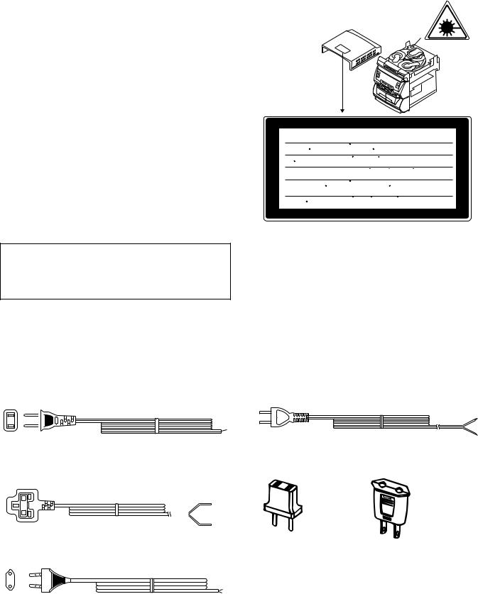
Precaution to be taken when replacing and servicing the Laser Pickup.
The AEL (Accessible Emission Level) of Laser Power Output for this model is specified to be lower than Class I Requirements. However, the following precautions must be observed during servicing to protect your eyes against exposure to the Laser beam.
(1)When the cabinet has been removed, the power is turned on without a compact disc, and the Pickup is on a position outer than the lead-in position, the Laser will light for several seconds to detect a disc. Do not look into the Pickup Lens.
(2)The Laser Power Output of the Pickup inside the unit and replacement service parts have already been adjusted prior to shipping.
(3)No adjustment to the Laser Power should be attempted when replacing or servicing the Pickup.
(4)Under no circumstances look directly into the Pickup Lens at any time.
(5)CAUTION - Use of controls or adjustments, or performance of procedures other than those specified herein may result in hazardous radiation exposure.
Laser Diode Properties
Material: GaAIAs
Wavelength: 780 nm
Emission Duration: continuous
Laser Output: max. 0.6 mW
CAUTION-INVISIBLE LASER RADIATION WHEN OPEN. DO NOT STARE INTO BEAM OR VIEW DIRECTLY WITH OPTICAL INSTRUMENTS.
VARNING-OSYNLIG LASERSTRALNING NAR DENNA DEL AR OPPNAD. STIRRA EJ IN I STRALEN OCH BETRAKTA EJ STRALEN MED OPTISKA INSTRUMENT.
ADVERSEL-USYNLIG LASERSTRALING VED ABNING. SE IKKE IND I STRALEN-HELLER IKKE MED OPTISKE INSTRUMENTER.
VARO! AVATTAESSA OLET ALTTIINA NAKYMATON LASERSATEILYLLE. ALA TUIJOTA SATEESEEN ALAKA KATSO SITA OPTISEN LAITTEEN LAPI.
VARNING-OSYNLIG LASERSTRALNING NAR DENNA DEL AR OPPNAD. STIRRA EJ IN I STRALEN OCH BETRAKTA EJ STRALEN GENOM OPTISKT INSTRUMENT.
ADVERSEL-USYNLIG LASERSTRALING NAR DEKSEL APNES. STIRR IKKE INN I STRALEN ELLER SE DIREKTE MED OPTISKE INSTRUMENTER.
VOLTAGE SELECTION
The voltage selector is located on the AC voltage selector box. If adjustment is necessary, use a screwdriver in order to turn the selector in either direction until the correct voltage figure is displayed in the window next to the adjisument screw.
QACCA0001AW00 |
|
|
|
|
||||
|
92LCoRDT1699A |
|||||||
|
|
|
|
|
|
|
|
|
|
|
|
|
|
|
|
|
|
|
|
|
|
|
|
|
|
|
|
|
|
|
|
|
|
|
|
|
|
|
|
|
|
|
|
|
QACCB0003AW00 |
|
92LPLUG027 |
92LPLUG155A |
||||||||
|
|
|
|
|
|
|
|
|
|
|
|
|
|
|
|
|
|
|
|
|
|
|
|
|
|
|
|
|
|
|
|
|
|
|
|
|
|
|
|
|
|
|
|
|
|
|
|
QACCE0008AW00
Figure 2 AC POWER SUPPLY CORD AND AC PLUG ADAPTOR
– 2 –
CD-C440W/CP-C440W
FOR A COMPLETE DESCRIPTION OF THE OPERATION OF THIS UNIT, PLEASE REFER TO THE OPERATION MANUAL.
SPECIFICATIONS
CD-C440W
 General
Power source: |
AC 110/127/220/230-240 V, 50/60 Hz |
Power consumption: |
200 W |
Dimensions: |
Width; 270 mm (10-5/8") |
|
Height; 300 mm (11-13/16") |
|
Depth; 368 mm (14-1/2") |
Weight: |
6.9 kg (15.2 lbs.) |
 Amplifier section
Output power: |
PMPO; 800 W (total) |
|
MPO; 192 W (96 W + 96 W) (10% T.H.D) |
|
RMS; 100 W (50 W + 50 W) (10% T.H.D) |
Input terminals: |
Video/Auxiliary (audio signal) x 2; |
|
500 mV/47 kohms |
Output terminals: |
Speakers; 6 ohms |
|
Headphones; 16-50 ohms |
|
(recommended; 32 ohms) |
 Compact disc player section
Type: |
3-disc multi-play compact disc player |
Signal readout: |
Non-contact, 3-beam semi-conductor |
|
laser pickup |
D/A Converter: |
1-bit D/A converter |
Frequency response: |
20 - 20,000 Hz |
Dynamic range: |
90 dB (1 kHz) |
 Tuner section
Frequency range: |
FM; 88 - 108 MHz |
|
MW; 531 - 1,602 kHz |
 Cassette deck section
Type: |
Compact cassette tape |
Frequency response: |
50 - 14,000 Hz (Normal tape) |
Motor: |
DC motor with electronic governor x 1 |
Signal/noise ratio: |
55 dB (TAPE 1, playback) |
|
50 dB (TAPE 2, recording/playback) |
Bias and erasure |
|
system: |
AC |
Tape speed: |
4.76 cm/sec. (1-7/8 ips) |
Wow and flutter: |
0.15 % (WRMS) |
Heads: |
TAPE-1: Playback x 1 |
|
TAPE-2: Record/playback x 1 |
|
Erase x 1 |
CP-C440W
 Speaker section
Type: |
2-way 160 mm (6-1/2") woofer and |
|
50 mm (2") tweeter type |
Maximum input power: 100 W |
|
Impedance: |
6 ohms |
Dimensions: |
Width; 220 mm (8-11/16") |
|
Height; 300 mm (11-13/16") |
|
Depth; 247 mm (9-3/4") |
Weight: |
3.4 kg (7.5 lbs.)/each |
Specifications for this model are subject to change without prior notice.
– 3 –
CD-C440W/CP-C440W
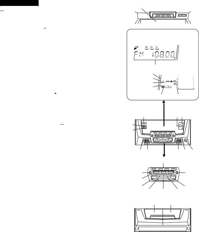
NAMES OF PARTS
CD-C440W

 Front Panel
1.Disc Tray
2.Disc Number Selector Buttons
3.Disc Skip Button
4.Open/Close Button: 
1 |
2 |
3 4 |
|||||
|
|
|
|
|
|
|
|
|
|
|
|
|
|
|
|
|
|
|
|
|
|
|
|
|
|
|
|
|
|
|
|
|
|
|
|
|
|
|
|
5.CD Play Indicator: 
6.CD Repeat Indicator: 
7.CD Pause Indicator: 

8.Disc Number Indicators
9.Function/CD Track/Preset Channel/Volume/
Frequency/CD Counter/Time/Sleep Time Indicator
10.3D Surround Indicator
11.Sleep Indicator
12.FM Stereo Moke Indicator:ST
13.FM Stereo Indicator: 
14.Extra Bass Indicator: X-BASS
15.Memory Indicator
16.Direction Indicators
17.Reverse Mode Indicator: 
18.Record Indicator
19.Timer Indicator
20.Spectrum Analyzer/Volume Level Indicator
21.On/Stand-by Switch
22.Extra Bass Button: X-BASS
23.Volume Up/Down Buttons: 

24.Clock Button
25.Timer/Sleep Button
26.Memory/Set Button
27.Tuning and Time Up/Down Buttons: 

28.Editing Speed Selector Buttons: NORMAL/HIGH
29.Reverse Mode Button
30.Headphone Socket
31.Function Selector Buttons
32.Record Pause Button: 


33.3D Surround Mode Select Buttons: PASS/MONO/STEREO
34.Track Down/Review/Preset Down Button: 


35.(TAPE 2) Reverse Play Button: 
36.Stop Button: 
37.(TAPE 1) Play Button/(TAPE 2) Forward Play Button/ (CD) Play/Repeat Button: 
38.Track Up/Cue/Preset Up Button: 


39.Equalizer Selector/Demo Mode Button
40.(TAPE 1) Cassette Compartment
41.(TAPE 2) Cassette Compartment
5 |
6 7 |
|
|
8 |
|
|
|
|
||||
|
|
|
|
|
|
|
|
|
|
|
|
|
|
|
|
|
|
|
1 |
2 |
3 |
|
|
|
|
|
|
|
|
|
|
|
|
|
|
|
|
|
9 |
10 11 |
|
|
|
|
|
|
|
|
|||||||
12 |
|
|
|
|
|
|
|
|
|
|
|
|
|
|
|
|
13 |
|
|
|
|
|
|
|
|
|
|
|
|
|
|
|
|
|
|
ST |
SLEEP |
|
|
|
|
|
|
|
|
|
|
|
||
14 |
|
kHz X-BASS |
|
|
|
|
|
|
|
|
|
|
||||
|
|
|
|
|
|
|
|
|
|
|
||||||
|
|
|
|
|
||||||||||||
15 |
|
MHz MEMORY |
|
|
|
|
|
|
|
|
|
|
||||
|
|
|
REC |
63 |
250 |
1k 4k 16k |
||||||||||
|
|
|
|
|
|
|
|
|
|
|
|
|
|
|
|
|
|
16 171819 20 |
|
|
|||||||||||||
21 |
22 23 |
|
|
|
|
|
||||||||||
24
25
26 27 |
|
28 29 30 |
|
31 |
|
32 |
|
39 |
33 |
|
|
34 |
|
38 |
35 |
36 |
37 |
|
|
|
40 |
|
41 |
– 4 –

CD-C440W

 Rear Panel
1.Video/Auxiliary (Audio Signal) Input Sockets
2.Span Selector Switch
3.AC Voltage Selector
4.AC Power Lead
5.FM 75 ohms Aerial Terminal
6.Aerial Earth Terminal
7.AM Aerial Terminal
8.Speaker Terminals
CP-C440W

 Speaker Section
9.Tweeter
10.Bass Reflax Ducts
11.Woofer
12.Speaker Wire
CD-C440W

 Remote Control
1. Remote Control Transmitter LED
 CD Control section
2.Disc Number Select Button
3.Track Down/Review Button: 


4.Track Up/Cue Button: 


5.Disc Skip Button
6.Play/Repeat Button: 
7.Stop Button: 
8.Memory Button
9.Clear Button
10.Random Button
11.Pause Button: 

 Tuner control section
12. Preset Up/Down Buttons: 

 Tape control section
13.(TAPE 1/2) Stop Button: 
14.(TAPE 2) Reverse Play Button: 
15.(TAPE 2) Record Pause Button: 


16.(TAPE 1) Play Button/
(TAPE 2) Forward Play Button: 
17.(TAPE 2) Rewind Button: 
18.(TAPE 2) Fast Forward Button: 
19.Function Selector Buttons
20.3D Surround Mode Buttons: PASS/MONO/STEREO
21.Equalizer Mode Button
22.On/Stand-by Button
23.Extra Bass Button: X-BASS
24.Volume Up/Down Buttons: 

CD-C440W/CP-C440W
1 |
|
2 |
5 |
3 |
6 |
7 |
|
4 |
8 |
9 |
10 |
11 |
12
1
2 
 5 3
5 3 


 6
6
4 |
9 |
7 |
8 |
10 11 |
|
|
|
12 |
13 |
|
16 |
14 |
|
17 |
|
|
|
15 |
|
18 |
19 |
|
|
20 |
|
21 |
22 |
|
|
23 |
24 |
|
– 5 –
– 6 –
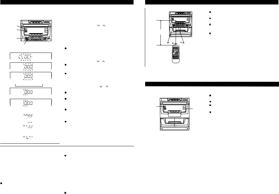
SETTING THE CLOCK
In this example, the clock is set for the 24-hour (0:00) system.
ON/
STAND-BY
CLOCK
MEMORY/
SET
TUNING/TIME (
 )
)
2
3
4
0:00 
 AM 0:00
 AM 12:00
5
6
7 
8 
9 
To change the time display mode:
1 Press the ON/STAND-BY switch to enter the standby mode.
2 Press the VOLUME button, the TUNING/TIME button and the ON/STAND-BY switch all at the same time. Hold them down for at least 1 second.
3 Perform steps 1 - 9 above.
Note:
The operation explained above will erase all data stored in memory, such as clock and timer settings, tuner and CD presets.
1 |
Press the ON/STAND-BY switch to enter the stand-by mode. |
|||
2 |
Press the CLOCK button. |
|
|
|
3 |
Within 5 seconds, press the MEMORY/SET button. |
|||
4 |
Press the TUNING/TIME ( |
or |
) button to select the time |
|
|
display mode. |
|
|
|
|
"0:00" |
→ The 24-hour display will appear. |
||
|
|
(0:00 - 23:59) |
|
|
|
"AM 0:00" → The 12-hour display will appear. |
|||
|
|
(AM 0:00 - PM 11:59) |
||
|
"AM 12:00" → The 12-hour display will appear. |
|||
|
|
(AM 12:00 - PM 11:59) |
||
|
Note that this can only be set when the unit is first installed |
|||
5 |
or it has been reset (see below). |
|
||
Press the MEMORY/SET button. |
|
|||
6 |
Press the TUNING/TIME ( |
or |
) button to adjust the hour. |
|
|
Press the TUNING/TIME button once to advance the time by |
|||
|
1 hour. Press for more than 0.5 seconds to advance continu- |
|||
|
ously. |
|
|
|
|
When the 12-hour display is selected, "AM" will change auto- |
|||
7 |
matically to "PM". |
|
|
|
Press the MEMORY/SET button. |
|
|||
8 |
Press the TUNING/TIME ( |
or |
) button to adjust the |
|
|
minutes. |
|
|
|
|
Press the button for at least 0.5 seconds to change the time |
|||
|
in 5-minute intervals. |
|
|
|
|
The hour setting will not advance even if minutes advance |
|||
9 |
from "59" to "00". |
|
|
|
Press the MEMORY/SET button. |
|
|||
|
The clock starts operating from "0" seconds. (Seconds are |
|||
|
not displayed.) |
|
|
|
Note:
In the event of a power failure or when the AC power lead is disconnected, the clock display will go out.
When the AC power supply is restored, the clock display will flash on and off to indicate the time when the power failure occurred or when the AC power lead was disconnected.
If this happens, follow the procedure below to change the clock time.
To change the clock time:
When the ON/STAND-BY switch is set to STAND-BY.
When the unit is in the demonstration mode, press the DEMO button to enter the clock mode.
Press the MEMORY/SET button.
Perform steps 6 - 9 above.
When the ON/STAND-BY switch is set to ON.
Press the CLOCK button.
Within 5 seconds, press the MEMORY/SET button.
Perform steps 6 - 9 above.
To see the time display: (When the power is ON)
Press the CLOCK button.
The time display will appear for about 5 seconds.
PREPARATION FOR USE
0.2 m - 6 m (8" - 20')
15 |
15 |
|
Notes concerning use:
Replace the batteries if control distance decreases or operation becomes erratic.
Periodically clean the transmitter LED on the remote control and the sensor on the main unit with a soft cloth.
Exposing the sensor on the main unit to strong light may interfere with operation. Change the lighting or the direction of the unit.
Keep the remote control away from moisture, excessive heat, shock, and vibrations.
C440W-C440W/CP-CD
RESETTING THE MICROCOMPUTER
1 |
2 |
|
2 


Reset the microcomputer under the following conditions:
To erase all of the stored memory contents (clock and timer settings, tuner and CD presets).
If the display is not correct.
If the operation is not correct.
Note:
To erase the tuner preset memory, see "To erase all of the contents of preset memory" on page 16.
1 Press the ON/STAND-BY switch to enter the stand-by mode.
2 Press the VOLUME  button, the TUNING/TIME
  button and the ON/STAND-BY switch all at the same time. Hold them down for at least 1 second.
MANUAL OPERATION
CD-C440W/CP-C440W
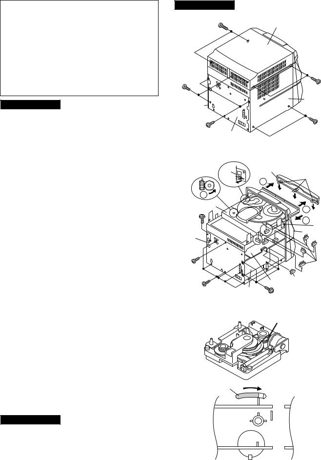
DISASSEMBLY
Caution on Disassembly
Follow the below-mentioned notes when disassembling the unit and reassembling it, to keep it safe and ensure excellent performance:
1.Take cassette tape and compact disc out of the unit.
2.Be sure to remove the power supply plug from the wall outlet before starting to disassemble the unit.
3.Take off nylon bands or wire holders where they need be removed when disassembling the unit. After servicing the unit, be sure to rearrange the leads where they were before disassembling.
4.Take suffcient care on static electricity of integrated circuits and other circuits when servicing.
CD-C440W
STEP |
REMOVAL |
|
PROCEDURE |
|
FIGURE |
|
|
|
|
|
|
1 |
Top Cabinet |
1. Screw ..................... |
(A1) x4 |
7-1 |
|
|
|
|
|
|
|
2 |
Side Panel |
1. Screw ..................... |
(B1) x6 |
7-1 |
|
|
(Left/right) |
|
|
|
|
|
|
|
|
|
|
3 |
CD Player Unit/ |
1. |
Turn on the power supply, |
7-2 |
|
|
CD Tray Cover |
|
open the disc tray, take out |
|
|
|
|
|
the CD cover, and close. |
|
|
|
|
|
(Note 1) |
|
|
|
|
2. |
Hook ....................... |
(C1) x3 |
|
|
|
3. |
Hook ....................... |
(C2) x2 |
|
|
|
4. |
Screw ..................... |
(C3) x1 |
|
|
|
5. |
Socket .................... |
(C4) x4 |
|
|
|
|
|
|
|
4 |
Tuner PWB |
1. Screw ..................... |
(D1) x4 |
7-2 |
|
|
|
2. |
Soket ...................... |
(D2) x1 |
|
|
|
|
|
|
|
5 |
Back Board |
1. Screw ..................... |
(E1) x6 |
7-2 |
|
|
|
2. |
Screw ..................... |
(E2) x1 |
|
|
|
|
|
|
|
6 |
Main PWB |
1. Screw ..................... |
(F1) x3 |
8-1 |
|
|
|
2. |
Holder .................... |
(F2) x2 |
|
|
|
3. |
Flat Wire ................. |
(F3) x4 |
|
|
|
4. |
Socket .................... |
(F4) x3 |
|
|
|
|
|
|
|
7 |
Headphones PWB |
1. |
Screw ..................... |
(G1) x1 |
8-1 |
|
|
|
|
|
|
8 |
Front Panel |
1. Screw ..................... |
(H1) x2 |
8-1 |
|
|
|
|
|
|
|
9 |
Display PWB/ |
1. Screw ..................... |
(J1) x3 |
8-2 |
|
|
Switch PWB |
2. Screw ..................... |
(J2) x11 |
|
|
|
|
|
|
|
|
10 |
Tape Mechanism |
1. |
Open the cassette holder. |
8-2 |
|
|
|
2. |
Screw...................... |
(K1) x6 |
|
|
|
|
|
|
|
11 |
Power Amp. PWB |
1. |
Screw ..................... |
(L1) x4 |
8-3 |
|
|
|
|
|
|
12 |
Turntable |
1. Screw ..................... |
(M1) x1 |
8-4 |
|
|
|
2. |
Cover ..................... |
(M2) x1 |
|
|
|
|
|
|
|
13 |
Disc Tray |
1. Screw ..................... |
(N1) x2 |
8-4 |
|
|
|
2. |
Guide ..................... |
(N2) x2 |
|
|
|
|
|
|
|
14 |
CD Changer |
1. Screw ..................... |
(P1) x4 |
8-5 |
|
|
Mechanism |
|
|
|
|
15 |
CD Mechanism |
1. Screw ..................... |
(Q1) x1 |
8-5 |
|
|
|
|
|
|
|
Note 1:
How to open the changer manually. (Fig. 7-3)
1.Insert the tip of fine screwdriver into the hole of CD player base, and press down the worm wheel < A > .
2.Then, turn fully the lock lever in the arrow direction through the hole on the loading chassis bottom in this state.
After that, push forward the CD player base.
CP-C440W
CD-C440W
( A1 ) x2 |
Top Cabinet |
|
|
ø3 x12mm |
|
( A1 ) x2
ø3 x12mm
( B1 ) x2
ø3 x8mm
|
Side Panel |
Side Panel |
(Left) |
(Right) |
|
( B2 ) x2 |
( B1 ) x2 |
ø3 x8mm |
|
Rear Panel |
ø3 x8mm |
Figure 7-1
(C2)x1 |
CD Tray Cover |
Hook |
Pull |
|
( C1) x3 |
1 |
|
|
|
|
|
A |
|
|
CD Player Unit |
|
1 |
|
|
|
( E2 ) x1 |
|
2 |
ø3 x10mm |
|
|
|
( C2 ) x1 |
|
|
|
|
Back |
|
Front Panel |
|
|
|
Board |
|
|
( C3 ) x1 |
|
|
ø3 x8mm |
|
|
|
|
( C4 ) x4 |
|
|
( D2 ) x1 |
( E1 ) x6 |
Main PWB |
|
Tuner |
|
|
ø3 x8mm |
|
|
PWB ( D1 ) x4 |
|
|
|
|
|
|
ø3 x10mm |
|
|
Figure 7-2 |
|
|
< A > |
|
LOCK
LEVER
STEP |
REMOVAL |
|
PROCEDURE |
|
FIGURE |
|
|
|
|
|
|
1 |
Speaker |
1. |
Net Frame Ass'y ..... |
(A1) x1 |
8-6 |
|
|
2. Duct Front Panel .... |
(A2) x1 |
|
|
|
|
3. |
Screw ...................... |
(A3) x4 |
8-7 |
|
|
4. |
Screw ...................... |
(A4) x4 |
|
|
|
|
|
|
|
Figure 7-3
– 7 –
CD-C440W/CP-C440W
Headphone |
|
( F3 ) x2 |
||
|
Front Panel |
|||
PWB |
( F4 ) x3 |
|||
|
|
|||
( G1 ) x1 |
|
|
( F2 ) x2 |
|
|
|
|
||
ø3 x11mm |
|
|
|
|
|
|
|
( F3 ) x1 |
|
( F1 ) x1 |
|
|
( F1 ) x1 |
|
ø3 x10mm |
|
|
||
|
|
ø3 x10mm |
||
( F3 ) x1 |
|
|
||
|
Push |
|
||
|
|
|
||
|
|
|
Push |
|
|
|
|
Tape |
|
|
|
|
Mechanism |
|
|
|
|
( F1 ) x1 |
|
Main PWB |
ø3 x10mm |
|||
( H1 ) x2 |
||||
|
|
|
||
|
|
|
ø3 x8mm |
|
|
|
Figure 8-1 |
|
|
( J1 ) x3 |
|
Switch PWB |
||
ø3 x10mm |
|
Front Panel |
||
|
|
|
||
|
|
|
Display |
|
( J2 ) x11 |
|
PWB |
||
ø3 x10mm |
|
Open |
||
|
|
|
||
( K1 ) x6 |
|
|
|
|
ø3 x10mm |
|
|
||
|
|
Tape |
Cassette |
|
|
|
Mechanism |
Holder |
|
|
|
|
(Left/Right) |
|
Figure 8-2
Power Supply PWB
( L1 ) x4 ø3 x10mm
Power Amp.
PWB
Figure 8-3
( M1 ) x1 ø3 x10mm 
( M2 ) x1
Turntable
( N1 ) x1 |
Disc Tray |
|
|
ø3 x10mm |
|
( N2 ) x1
( N1 ) x1 ø3 x10mm
CD Player Unit |
( N2 ) x1 |
|
Figure 8-4
 ( P1 ) x4
 ø3 x12mm
( Q1 ) x1 ø2.6 x10mm
Shift Lever
CD Changer
Mechanism
CD Player Base |
CD Mechanism |
Care when installing the CD changer mechanism.
Install the CD changer mechanism on the CD player base after the shift lever has been set in the highest position.
Figure 8-5
CP-C440W
(A1) x1
SHARP 
Speaker Box
Screw
driver
Driver should be pried  away from speaker Box.
Direction of handle
Figure 8-6
(A3) x4  ø3 x10mm
Speaker Box
(A2) x1
Woofer
(A4) x4
ø4 x12mm
Figure 8-7
– 8 –
CD-C440W/CP-C440W
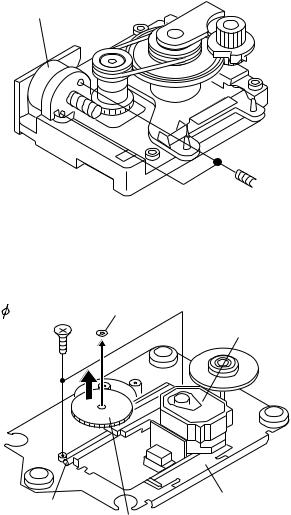
REMOVING AND REINSTALLING THE MAIN PARTS
CD MECHANISM SECTION
Perform steps 1, 2, 3, 14 and 15 of the disassembly method to remove the CD mechanism.
How to remove the turntable up/down motor (See Fig. 9-1)
1.Remove the screws (A1) x 2 pcs., to remove the turntable up/down motor.
How to remove the pickup (See Fig. 9-2)
1.Remove the screws (B1) x 2 pcs., to remove the shaft (B2).
2.Remove the stop washer (B3) x 1 pc., to remove the gear (B4).
3.Remove the pickup.
Turntable Up/Down Motor
( A1 ) x2  ø2 x5mm
Figure 9-1
( B1 ) x2 |
Stop Washer |
|
( B3 ) x1 |
||
2.6 x6mm |
||
|
Pickup
Shaft |
CD Mechanism |
|
Gear |
||
( B2 ) x1 |
||
( B4 ) x1 |
||
|
||
|
Figure 9-2 |
– 9 –
CD-C440W/CP-C440W
ADJUSTMENT
MECHANISM SECTION
• Driving Force Check
Torque Meter |
Specified Value |
|
|
Play: TW-2412 |
Tape 1: Over 80 g |
|
Tape 2: Over 80 g |
|
|
• Torque Check
Torque Meter |
Specified Value |
|
|
|
|
|
Tape 1 |
Tape 2 |
|
|
|
Play: TW-2111 |
30 to 60 g. cm |
30 to 100 g.cm |
|
|
|
Fast forward: TW-2231 |
— |
50 to 100 g.cm |
|
|
|
Rewind: TW-2231 |
— |
50 to 100 g.cm |
|
|
|
• Tape Speed |
|
|
|
Test Tape |
Adjusting |
Specified |
Instrument |
|
|
Point |
Value |
Connection |
|
|
|
|
|
Normal |
MTT-111 |
VRM1 |
3,000 ± |
Speaker |
speed |
|
|
30 Hz |
terminal |
|
|
|
|
|
TAPE
SPEED
VRM1
TUNER SECTION
fL: Low-range frequency fH: High-renge frequency
• AM IF/RF
Signal generator: 400 Hz, 30%, AM modulated
Test Stage |
Frequency |
Frequency |
Setting/ |
Instrument |
|
|
|
|
Display |
Adjusting |
Connection |
|
|
|
|
Parts |
|
IF |
450 kHz |
|
1,602 kHz |
T351 |
*1 |
|
|
|
|
|
|
AM Band |
— |
|
531 kHz |
(fL): T306 |
*2 |
Coverage |
|
|
|
1.1 ± 0.1 V |
|
|
|
|
|
|
|
AM |
990 kHz |
|
990 kHz |
(fL): T302 |
*1 |
Tracking |
|
|
|
|
|
|
|
|
|
|
|
*1. Input: Antenna, |
Output: TP302 |
|
|
||
*2. Input: Antenna, |
Output: TP301 |
|
|
||
•FM Notes:
1: Description of the "FM IF Adjustment" is not carried on this Manual. It is because the IF coil in the FM front end section has been best adjusted in the factory so that its further adjustment is not needed at the field. When replacing the FM front end assembly, no adjustment is needed either.
2: The parts in the FM front end section are prepared in a complete unit, so you can't obtain each part individually
•FM Mute Level
Signal generator: 1 kHz, 40 kHz dev., FM modulated
Frequency |
Frequency |
Adjusting |
Instrument |
|
Display |
Parts |
Connection |
|
|
|
|
98.00 MHz |
98.00 MHz |
VR351* |
Input: Antenna |
(25 dBμV) |
|
|
Output: Speaker |
|
|
|
Terminal |
TAPE MECHANISM PWB
TUNER PWB
VR351 |
FM MUTE |
|
|
T351 |
LEVEL |
FE301 |
SO301 |
|
|
ANTENNA |
|
|
|
|
|
|
|
|
TERMINAL |
AM IF |
T306 |
|
|
|
|
|
|
AM BAND |
|
|
|
COVERAGE |
|
|
|
IC303 |
|
|
|
|
|
T302 |
|
TP302 |
|
|
AM |
|
|
|
TRACKING |
Figure 10 ADJUSTMENT POINTS
– 10 –
CD-C440W/CP-C440W
TEST MODE
• Setting the test mode
Any one of test mode can be set by pressing several keys as follows. <REC. PAUSE> + <CD> + <POWER> TEST: CD operation test
• TEST mode
Function — CD test mode
Setting of TEST mode
Indication of CD TST mode (Fig. 11-1)
|
OPEN/CLOSE operation is manual operation. |
) or ( |
) key. |
|
IL is not performed. |
||||||
|
|||||||||||
|
|
|
|
|
|||||||
|
|
|
|
|
|
|
|||||
The pickup can be moved by using the ( |
|
|
|||||||||
|
|
|
|||||||||
|
|
<MEMORY> |
|
<MEMORY> |
|
<MEMORY> |
<STOP> |
||||
|
|
LASER ON |
|
Tracking on the spot. |
|
|
Tracking on the spot. |
|
STOP |
||
|
|
|
|
SERVO OFF PLAY |
|
|
SERVO ON PLAY |
|
|
||
|
|
<PLAY> key input |
|
TOC. IL is performed, and the ordinary PLAY is performed. |
|
Press <STOP> key. |
|
Stop |
||||
|
|
|
|
|
||||||||
|
|
|
|
|
If the following key is pressed during PLAY, it is possible |
|
|
|
|
|||
|
|
|
|
|
to specify directly any Track No. |
|
|
|
|
|
|
|
|
|
|
|
|
<Disc Number 1> key: Track 4 |
|
|
|
|
|
|
|
|
|
|
|
|
<Disc Number 2> key: Track 9 |
|
|
|
|
|
|
|
|
|
|
|
|
<Disc Number 3> key: Track 15 |
|
|
|
|
|
|
|
Note: |
|
|
|
|
|
|
|
|
|
|
||
Only in STOP state it is possible to slide the pickup with the ( |
) or ( |
) key. |
|
|
|
|
||||||
VOL. --- |
Last memory |
|
|
|
|
|
|
|
|
|
||
|
|
|
|
|
|
|
|
|
||||
BAL. --- |
CENTER |
|
|
|
|
|
|
|
|
|
||
R.GEQ. |
--- FLAT |
|
|
|
|
|
|
|
|
|
||
X-BAS --- |
OFF |
|
|
|
|
|
|
|
|
|
||
Canceling method - POWER OFF
Figure 11-1
CD SECTION
Since this CD system incorporates the following automatic adjustment function, when the pickup is replaced, it is not necessary to readjust it.
Since this CD unit does not need adjustment, the combination of PWB and laser pickup unit is not restricted.
• Automatic adjustment item
1.Focus offset (Fig. 11-2)
2.Tracking offset (Fig. 11-3)
3.E/F balance (tracking error balance) (Fig. 11-4)
4.RF level AGC function (HF level: constant)
5.RF level automatic follow-up of the tracking gain
This automatic adjustment is performed each time a disc is changed. Therefore, each disc is played back using the optimal settings.
0.1s
0.50 V
IC1 20 FE
FOCUS
OFF-SET
ADJUST
0.1s
0.50 V
IC1 7 TE  TRACKING OFF-SET
1 ADJUST
|
2 |
|
|
Figure 11-2 |
|
200 ms |
TRACKING/ |
|
1V/diV |
ERROR |
|
IC 1 15 |
BARANCE |
|
TO |
1 ADJUST |
|
|
||
200 ms |
|
|
1V/diV |
|
|
IC 1 7 |
2 |
|
TE |
||
|
||
|
Figure 11-4 |
10ms 0.50 V
IC1 20 FE
10ms 0.50 V IC1 7 TE
Figure 11-3
Enlarged
View
TRACKING
OFF-SET 1 ADJUST
2
– 11 –
CD-C440W/CP-C440W
NOTES ON SCHEMATIC DIAGRAM
∙Resistor:
To differentiate the units of resistors, such symbol as K and M are used: the symbol K means 1000 ohm and the symbol M means 1000 kohm and the resistor without any symbol is ohm-type resistor. Besides, the one with “Fusible” is a fuse type.
∙Capacitor:
To indicate the unit of capacitor, a symbol P is used: this symbol P means micro-micro-farad and the unit of the capacitor without such a symbol is microfarad. As to electrolytic capacitor, the expression “capacitance/withstand voltage” is used.
(CH), (TH), (RH), (UJ): Temperature compensation (ML): Mylar type
(P.P.): Polypropylene type
∙Schematic diagram and Wiring Side of P.W.Board for this model are subject to change for improvement without prior notice.
∙The indicated voltage in each section is the one measured by Digital Multimeter between such a section and the chassis with no signal given.
1.In the tuner section, ( ) indicates AM
< > indicates FM stereo
2.In the main section, a tape is being played back.
3.In the deck section, a tape is being played back. ( ) indicates the record state.
4.In the power section, a tape is being played back.
5.In the CD section, the CD is stopped.
∙Parts marked with “ ” (
” ( 


 ) are important for maintaining the safety of the set. Be sure to replace these parts with specified ones for maintaining the safety and performance of the set.
REF. NO |
DESCRIPTION |
POSITION |
|
|
|
SW1 |
OPEN/CLOSE |
ON—OFF |
|
|
|
SW2 |
MWCHA UP |
ON—OFF |
|
|
|
SW3 |
DISC NUMBER |
ON—OFF |
|
|
|
SW4 |
PICKUP IN |
ON—OFF |
|
|
|
SW601 |
SPAN SELECTOR |
50/9—100/10 |
|
|
|
SW701 |
ON/STAND-BY |
ON—OFF |
|
|
|
SW702 |
CLOCK |
ON—OFF |
|
|
|
SW703 |
TIME/SLEEP |
ON—OFF |
|
|
|
SW704 |
DISC 1 |
ON—OFF |
|
|
|
SW705 |
DISC 2 |
ON—OFF |
|
|
|
SW706 |
DISC 3 |
ON—OFF |
SW707 |
DISC SKIP |
ON—OFF |
|
|
|
SW708 |
OPEN/CLOSE |
ON—OFF |
|
|
|
SW709 |
CD |
ON—OFF |
SW710 |
TUNER/BAND |
ON—OFF |
|
|
|
SW711 |
TAPE |
ON—OFF |
|
|
|
SW712 |
VIDEO |
ON—OFF |
|
|
|
SW717 |
CENTER MODE/PHANTOM |
ON—OFF |
|
|
|
SW719 |
CENTER MODE/NORMAL |
ON—OFF |
|
|
|
SW721 |
DOLBY PRO LOGIC/BYPASS |
ON—OFF |
|
|
|
SW723 |
REC/PAUSE |
ON—OFF |
|
|
|
SW724 |
TUNING UP/TIME |
ON—OFF |
|
|
|
SW725 |
VOLUME UP |
ON—OFF |
|
|
|
REF. NO |
DESCRIPTION |
POSITION |
|
|
|
SW726 |
X-BASS |
ON—OFF |
|
|
|
SW728 |
STOP |
ON—OFF |
|
|
|
SW729 |
FWD |
ON—OFF |
|
|
|
SW730 |
FF |
ON—OFF |
|
|
|
SW731 |
MEMORY SET |
ON—OFF |
|
|
|
SW732 |
TUNING DOWN/TIME |
ON—OFF |
|
|
|
SW733 |
VOLUME DOWN |
ON—OFF |
|
|
|
SW734 |
EQUALIZER/DEMO |
ON—OFF |
|
|
|
SW735 |
3D SURROUND |
ON—OFF |
|
|
|
SW736 |
REVERSE MODE |
ON—OFF |
|
|
|
SW737 |
REV |
ON—OFF |
|
|
|
SW738 |
REW |
ON—OFF |
|
|
|
SW739 |
EDIT NORMAL |
ON—OFF |
|
|
|
SW740 |
EDIT HIGH |
ON—OFF |
|
|
|
SW801 |
VOLTAGE SELECTOR |
110—127— |
|
|
220—230/240 |
|
|
|
SWM 3 |
REC FWD |
ON—OFF |
|
|
|
SWM 4 |
REC RVS |
ON—OFF |
|
|
|
SWM 5 |
F.A.S. |
ON—OFF |
|
|
|
SWM 6 |
CAM |
ON—OFF |
|
|
|
FRONT
VIEW
E C B
(S) (G)(D)
(1) (2) (3)
2SA2878 A |
|
|
|
|
|
|
|
|
|
2SD2012 |
333GTH2 |
|||||||||
2SK246 GR |
|
FRONT |
|
2SC1845 F |
333YTH2 |
|||||||||||||||
2SC2236 Y |
|
|
KTA1271 Y |
|||||||||||||||||
|
|
VIEW |
|
333YTH4 |
||||||||||||||||
2SC380 O |
|
|
|
KTA1273 Y |
|
|
|
|
|
|
|
|
|
5N4GTN52 |
||||||
KRC102 M |
|
|
|
|
|
|
|
|
|
|
|
|
|
|
|
FRONT |
LMKD515B5N4YTN52 |
|||
KRC104 M |
|
|
|
|
|
|
|
|
|
|
|
|
|
|
|
|||||
KRA107 M |
|
|
|
|
|
|
|
|
|
|
|
|
|
|
|
VIEW |
|
|||
KRC107 M |
|
|
|
|
|
|
|
|
|
|
|
|
|
|
|
|
|
|
|
|
|
|
|
|
|
|
|
|
|
|
|
|
|
|
|
|
|
|
|
|
|
KTA1266 GR |
|
|
|
|
|
|
|
|
|
|
|
|
|
|
|
|
|
|
|
|
|
B C E |
|
|
|
|
|
|
|
|
|
|
|
||||||||
|
|
|
|
|
|
|
|
|
|
|
|
|||||||||
KTC3199 GR |
|
|
|
|
|
|
|
|
|
|
|
|
||||||||
(D)(G)(S) |
|
|
|
|
|
|
|
|
|
|
|
|||||||||
KTC3203 Y |
|
|
|
|
|
|
|
|
|
|
|
|||||||||
|
(3) (2) (1) |
|
|
|
|
|
|
|
|
|
|
|
||||||||
Figure 12 TYPES OF TRANSISTOR AND LED
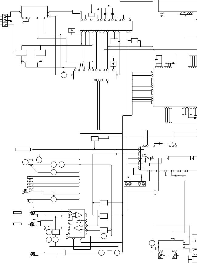
– 12 –

13 – |
BLOCK 13 Figure |
– |
DIAGRAM |
|
(1/3) |
PICKUP UNIT
FOCUS COIL
TRACKING COIL
M2 |
M1 |
SLED |
SPINDLE |
MOTOR |
MOTOR |
M |
M |
PICKUP IN
SW4
+4.9V
|
Q1 |
|
|
|
|
|
|
+4.9V |
|
|
|
|
|
|
|
|
|
|
|
|
|
XL1 |
|
|
|
|
|
|
|
|
|
||
|
|
|
|
|
|
|
|
|
|
|
|
|
|
|
||
|
62 |
64 |
|
|
|
45 |
44 |
6 23 36 41 43 |
|
|
|
|
|
|
|
|
|
LD0 |
VCC1 |
|
|
|
XIN |
XOUT |
VVDD VDD LVDD RVDD XVDD |
|
|
|
|
|
|
|
|
|
|
|
|
|
|
|
|
|
|
|
|
|
||||
|
|
|
|
|
|
|
IC2 |
|
LCHO37 |
|
|
|
|
|
|
|
|
|
|
|
|
|
|
|
|
|
|
|
|
|
|
|
|
|
|
IC1 |
|
|
|
|
LC78623E |
LVSS 38 |
|
|
|
|
|
|
|
|
|
|
|
|
|
|
RVSS 39 |
|
|
|
|
|
|
|
|||
|
|
|
|
|
|
|
|
|
|
|
|
|
|
|
||
|
LA9240M |
|
JP– 32 |
SERVO/SIGNALRCHO 40 |
|
|
|
|
|
|
|
|||||
|
|
9 EFMO |
CONTROL |
|
|
|
|
|
|
|
|
|||||
1 FIN2 |
|
|
|
~ |
10 EFMIN |
|
|
|
|
TO MAIN SECTION |
||||||
2 FIN1 SERVO AMP. |
CV+ 40 |
12 CLV+ |
|
SPEED H/L 27 |
|
|
|
|||||||||
|
|
|
|
|
|
|
|
|
|
|
|
|
|
|
||
3 E |
|
|
|
SLC 43 |
~ |
|
|
SOL 26 |
|
|
|
|
|
|
|
|
4 |
F |
|
|
|
SL1 44 |
20 JP– |
|
|
|
|
|
|
|
|
|
|
|
|
|
|
|
CONT1 24 |
|
|
|
|
|
|
|
||||
|
|
|
|
|
|
|
|
|
|
|
|
|
|
|
|
|
|
TO FD SPO SP SLD |
SL– SL+ |
DRF |
CL |
DAT CE |
RES. CQCK. COIN |
|
CONT2 25 |
|
|
|
|
|
CD O/C SW |
SW1 |
|
|
|
|
|
|
|
|
|
|
|
|
|
|
||||
|
|
|
|
|
|
|
|
|
|
|
|
|
|
|||
|
|
|
|
|
|
SQOUT. RWC. WRQ |
|
|
|
|
|
|
|
|
OPEN/CLOSE SW |
|
|
15 16 27 23 29 |
30 31 54 |
51 52 53 |
|
53 ~ 58 |
|
|
|
|
|
|
|
CD D.NO |
SW3 |
||
|
|
|
|
|
|
|
|
|
|
|
|
|
|
|
|
DISC NO |
|
|
|
|
|
|
|
|
|
|
|
|
|
|
|
CD U/D |
SW2 |
|
|
|
|
|
|
|
|
|
|
|
|
|
|
|
|
|
|
|
|
|
|
|
|
|
|
|
|
|
|
|
|
|
MEHCA UP |
|
|
|
|
|
CL, DAT, SELIAL CONTROL/CE |
|
|
|
|
DRIVER |
|
|
|
|
||
|
|
|
|
|
|
|
|
|
|
|
|
|
|
|
||
|
|
|
|
|
|
|
|
|
|
|
SWITCHING |
|
+B4 |
|
||
|
|
|
|
|
|
|
|
|
|
|
|
|
|
|
||
|
|
|
|
|
|
|
|
|
|
SPEED HIGHT/LOW |
Q94 |
|
|
|
|
|
|
|
|
|
|
|
|
|
|
|
|
|
|
|
|
|
|
|
|
|
|
SL+. SL–. DRF |
|
|
|
|
CONT2 |
|
|
8 |
2 |
6 |
M |
|
|
|
|
|
|
|
|
|
|
9 |
IC91 |
|
3 |
||||
|
|
|
|
|
|
|
|
|
|
CONT1 |
|
|
|
|||
|
|
|
|
|
|
|
|
|
|
|
1 |
LOADING MOTOR |
|
|||
|
|
|
|
|
|
|
|
|
|
|
|
DRIVER |
|
7 |
LOADING MOTOR |
|
|
5 22 32 |
|
|
|
|
|
|
|
|
|
|
|
5 |
|
|
|
|
|
|
|
|
|
|
|
|
|
|
+B2 |
|
|
UP/DOWN |
||
|
|
|
|
|
|
|
|
|
|
|
|
|
|
|||
6 |
|
|
20 |
|
+B4 |
|
|
|
|
|
|
|
|
|
|
|
7 |
IC5 |
|
26 |
|
|
|
|
|
|
SOL |
Q93 |
Q91 |
SOLM2 |
|
|
|
12 |
|
|
|
|
|
|
|
|
|
|
||||||
|
|
|
|
|
|
|
|
|
|
|
|
|||||
|
27 |
|
|
|
|
|
|
|
|
|
SOLENOID |
|
||||
13 |
M56748FP |
|
|
|
|
|
|
|
|
|
|
|
|
|
||
28 |
|
|
|
|
|
|
|
|
|
|
|
|
|
|||
|
|
|
|
|
|
|
|
|
|
|
|
|
|
|||
24 |
DRIVER |
29 |
|
|
|
|
|
|
|
|
|
|
|
|
|
|
25 |
|
|
34 |
|
|
|
|
|
|
|
|
|
|
|
|
|
30 |
|
|
35 |
|
|
|
|
|
|
|
|
|
|
|
|
|
31 |
|
|
36 |
|
|
|
|
|
|
|
|
|
|
|
|
|
|
8 9 10 11 |
|
|
|
|
|
|
|
|
|
|
|
|
|
|
|
|
|
|
|
|
PU-IN SW |
|
|
|
|
|
|
|
|
|
TO MAIN |
|
|
|
|
|
|
|
|
|
|
|
|
|
|
|
|
SECTION |
|
|
|
|
|
|
|
|
|
|
|
REGULATOR |
|
|
|
|
|
|
|
|
|
|
|
|
|
|
|
+4.9V |
|
Q81 |
|
+7.3V (B4) |
|
||
C440W-C440W/CP-CD
CD-C440W/CP-C440W
FM
AM
|
|
|
|
|
|
|
|
|
|
|
|
|
|
|
|
|
|
|
|
SM |
|
|
|
|
|
|
|
|
|
|
|
+B3 |
|
|
|
|
|
+B3 |
|
|
|
|
|
|
|
|
|
|
|
|
|
FM IF |
|
|
|
|
|
|
|
CF351 |
X351 |
|
|
|
|
|
||
|
|
|
|
|
|
|
AM IF |
|
|
|
|
|
|
|
|
|
|
|
|
|||
8 |
|
|
FE301 |
|
1 |
CF302 |
|
|
|
|
|
|
|
|
|
|
|
|
||||
|
FM FRONT END |
|
|
|
|
|
|
|
|
|
|
|
|
|
|
|
||||||
|
|
|
|
|
|
|
|
|
|
|
|
|
|
|
|
|
|
|
|
|||
|
|
|
|
|
5 |
FM IF IN |
|
T351 |
|
|
|
|
|
|
|
|
|
|
|
|
||
2 |
6 |
7 |
3 |
4 |
|
|
|
|
|
|
|
|
|
|
|
|
|
|
|
|||
|
|
1 |
2 |
|
|
|
4 |
|
|
8 |
9 |
|
|
|
|
|
|
|||||
|
|
|
OSC |
VT |
|
|
|
3 |
|
|
5 |
17 |
19 |
20 |
18 |
16 |
|
|||||
|
|
|
|
|
|
OUT |
REG |
|
IN GND |
|
VCC |
|
|
FM/AM |
MPX |
|
||||||
|
|
|
FM |
|
|
VR351 |
|
|
|
|
IC303 LA1832 |
|
|
OUT |
IN |
|
||||||
|
|
|
|
|
|
|
|
|
|
|
|
|
|
|||||||||
SO301 |
|
|
|
|
FM MUTE LEVEL |
AM |
|
FM IF DET/FM MPX/AM IF |
|
|
|
|||||||||||
|
|
|
|
|
|
|
|
|
|
|||||||||||||
ANTENNA |
|
|
|
|
|
|
OSC |
|
|
|
|
|
|
|
|
|
|
|
|
|
|
|
TERMINAL |
|
|
|
|
|
|
24 |
23 |
22 |
21 |
7 |
|
13 |
6 |
|
10 IF |
11 |
|
12 |
|
14 15 |
|
|
|
|
|
|
|
|
OUT |
IN |
AFC |
AMRF IN |
STEREO |
|
MONO/ST |
SD |
|
OUT |
|
|
|
L R |
|
|
|
|
|
|
|
FM OSC |
|
|
|
|
MPX |
MPX |
Q353 |
|
|||||||||
|
|
|
|
|
|
|
|
|
|
|
|
|
|
|
|
|
|
|
|
MUTING |
|
|
|
|
|
|
|
|
|
|
|
|
|
|
|
|
|
|
|
PHASE |
VCO |
Q354 |
|
||
|
|
|
|
|
|
|
|
|
|
|
|
|
|
|
|
|
CUT |
|
|
|||
AM RF |
|
|
|
|
|
|
|
|
|
|
|
|
|
|
|
|
|
TUNER MUTE |
|
|||
|
|
|
|
|
|
|
|
|
|
|
|
|
|
|
|
|
|
|
|
|||
AM ANT |
|
AM OSC |
|
|
|
|
|
|
|
|
|
|
|
|
|
|
|
|
SD |
|
||
|
|
|
|
|
|
|
|
|
|
|
|
|
|
|
|
|
|
|
|
|
|
|
T302 |
|
|
|
T306 |
|
|
|
|
|
|
|
|
|
|
|
VOLTAGE |
|
|
|
|
||
|
|
|
|
|
|
|
|
|
|
|
|
|
|
|
|
REGURATER |
|
|
|
|||
|
|
|
|
|
|
|
|
|
|
|
|
|
MONO/STFM |
|
|
|
+B3 |
|
|
|
|
|
|
|
|
|
|
|
X352 |
|
|
AMIN |
FMIN |
XT21 |
|
|
|
INIF |
|
|
|
|
|
|
|
|
|
|
|
|
|
4.5MHz |
|
|
|
|
|
|
|
|
|
|
|
|
|
|
|
|
|
|
|
|
|
+B3 |
|
|
|
|
|
|
|
|
|
|
|
+5V |
|
|
|
|
|
|
|
|
|
|
|
1 |
|
|
|
|
|
|
|
|
|
|
|
|
|
|
|
|
|
|
|
|
|
+B |
20 |
22 |
15 |
16 |
11 |
10 |
13 |
|
12 |
17 |
|
|
|
REC MUTE |
|
||
|
|
|
|
|
FM |
OSC |
|
|
IC302 |
|
|
|
|
|
|
|
|
|
80 |
|||
|
|
|
|
|
FM 7 |
|
|
|
|
|
|
|
|
|
|
|
|
HI SPEED |
|
|||
|
|
|
|
|
Q360 |
|
|
|
TC72131 |
|
|
|
|
|
8 |
|
|
76 |
||||
|
|
|
|
|
|
|
|
|
PLL(TUNER) |
|
|
|
|
|
|
|
BIAS |
|
||||
|
|
|
|
|
|
|
|
|
|
3 |
4 |
|
|
|
|
|
|
|
|
72 |
||
|
|
|
|
|
|
|
|
|
|
5 |
6 |
|
21 |
|
|
|
|
T1/T2 |
||||
|
|
|
|
|
|
|
|
|
|
CE |
DI |
CL DO |
|
|
|
|
|
|
PB MUTE |
70 |
||
|
|
|
|
|
|
|
|
|
|
|
|
|
|
|
|
T2 B-FP |
69 |
|||||
|
|
|
|
|
|
|
|
|
|
|
|
|
|
|
|
|
|
|
|
|
T2 A-FP |
68 |
|
|
|
|
|
|
|
|
|
|
|
|
|
|
|
|
|
|
|
|
|
|
67 |
|
|
|
|
|
|
|
|
|
|
|
|
|
|
|
|
|
|
|
|
|
TA MOT SW |
51 |
|
|
|
|
|
|
|
|
|
|
|
|
|
|
|
|
|
|
|
|
|
TA PUL |
|
|
|
|
|
|
|
|
|
|
|
|
|
|
|
|
|
|
|
|
|
|
TA MOT H/L |
50 |
|
|
|
|
|
|
|
|
|
|
|
|
|
|
|
|
|
|
|
|
|
|
49 |
|
|
|
|
|
|
|
|
|
|
|
|
|
|
|
|
|
|
|
|
|
TA CUM SW |
2331 |
|
|
|
|
|
|
|
|
|
|
|
|
|
|
|
|
|
|
|
|
|
T2 PH-OUT |
|
|
|
|
|
|
|
|
|
|
|
|
|
|
|
|
|
|
|
|
|
|
T1 RUN |
22 |
|
|
|
|
|
|
|
|
|
|
|
|
|
|
|
|
|
|
|
|
|
REC/PB |
2 |
CD MUTE
Q83
Q84
FROM CD UNIT
CD L 55
CL |
DI |
CE |
|
23 |
24 |
25 |
56 |
|
|
|
VDD |
R 57
|
|
|
+B2 |
|
|
|
|
|
|
|
|
|
|
TAPE |
L 53 |
|
|
MM1 |
|
MOTOR |
|
|
|
|
|
|
|
|
|
|
R 59 |
|
|
|
TAPE |
|
|
|
|
|
|
|
|
|
|
|
|
|
||
|
|
DRIVER |
|
|
|
|
|
|
|
|
|
TUNER |
L 54 |
|
||
|
MOTOR |
|
|
|
TA MOT SW |
|
|
|
|
|
|
|||||
|
|
QM02 |
|
|
|
|
|
|
|
|
|
R 56 |
|
|||
|
|
|
|
|
|
|
|
|
|
|
|
|
||||
|
M |
|
|
|
|
|
|
|
|
|
|
|
|
|
||
|
|
|
|
|
|
HI SPEED |
|
|
HI SPEED |
|
|
AUX |
L 52 |
|
||
|
|
|
QM01 |
QM04 |
|
|
|
|
|
R 60 |
|
|||||
|
|
|
|
|
|
|
|
|
|
|
|
|
||||
|
|
|
DRIVER |
|
|
|
|
|
|
|
|
|
AUX |
L 51 |
FRONT |
|
|
|
|
|
|
|
|
|
|
|
|
|
|
|
|||
|
|
|
|
|
SWITCHING |
|
|
|
|
|
|
|
|
R 61 |
IN |
|
|
|
|
|
QM05 |
|
TA MOT H/L |
|
|
|
|
|
|
|
48 64 |
||
|
|
|
|
|
|
|
|
|
|
|
|
|
|
LTIN RTIN |
||
|
|
|
DRIVER |
|
|
|
|
|
|
|
|
|
|
|
||
|
|
|
|
|
T2 A/B-FP |
|
|
|
|
|
|
|
|
|||
REC FWD |
|
|
|
|
|
|
|
|
|
|
|
|
|
|||
|
|
|
|
|
|
|
|
|
|
|
|
|
|
|
||
|
SWM3 |
|
|
|
|
|
T2 A/B-FP |
|
|
|
|
|
L R |
L |
R |
|
REC RVS |
|
|
|
|
|
|
|
|
|
|
||||||
|
|
|
|
|
|
|
|
|
|
|
|
J501 |
|
|
||
|
SWM4 |
|
|
|
|
|
TA CUM SW |
|
|
|
|
|
|
|
||
|
|
|
|
|
|
|
|
|
|
|
|
|
|
|||
CAM SW |
|
|
|
|
|
|
|
|
|
|
|
|
|
|
IN |
|
|
SWM6 |
|
|
|
|
|
T1 RUN SW |
|
|
|
|
|
|
|
||
|
|
|
|
|
|
|
|
|
|
|
|
|
|
|||
FAS SW |
|
|
|
|
|
|
|
|
|
|
VIDEO1 |
VIDEO2 |
||||
|
|
|
|
|
|
|
|
|
|
|
|
|||||
|
SWM5 |
|
|
|
|
|
|
|
|
|
|
|
|
|||
|
|
T2 PH-IN |
|
|
|
|
|
|
|
|
|
|
|
|
|
|
PHM1 |
|
+B2 |
|
|
|
|
|
|
|
|
|
|
|
|||
|
|
|
|
|
|
|
|
|
|
|
|
|
||||
|
|
|
|
|
|
|
|
|
|
|
|
|
|
|
||
|
|
|
|
|
|
|
T2 PH-OUT |
|
|
|
|
|
|
|
L-IN |
|
SOLENOID |
|
|
QM03 |
|
TA PUL |
|
|
PB MUTE |
|
|
|
|
|
|||
|
|
|
|
|
|
|
|
|
|
|
|
|||||
|
SOLM1 |
|
|
DRIVER |
|
|
IC101 |
|
Q117 |
|
|
|
|
|
||
|
|
|
|
|
|
|
Q118 |
|
|
|
|
|
||||
|
|
|
|
|
|
|
|
AN7345K |
|
MUTING |
|
|
|
|
|
|
|
|
|
|
|
|
PLAYBACK&RECORD AMP |
|
|
|
|
|
|||||
|
|
|
|
|
|
|
|
|
|
|
|
|||||
|
PB HEAD |
|
P.B |
|
L(T1) |
1 |
|
P.B. |
P.B |
|
|
|
|
|
|
|
TAPE 1 |
|
|
|
|
R(T1) |
24 |
|
REC MUTE |
|
|
|
|
||||
L-CH |
|
|
|
|
|
|
|
|
|
|
||||||
|
R-CH |
|
|
|
|
L(T2) |
2 |
|
4 |
L |
Q121 |
|
|
|
|
|
|
|
|
|
|
|
|
21 R |
|
|
|
|
|
||||
|
|
|
|
|
|
R(T2) |
23 |
|
Q122 |
|
|
|
|
|
||
|
|
|
|
|
|
|
|
|
|
|
|
|
|
|||
|
|
REC |
REC/PB |
|
L NF |
3 |
|
5 |
|
MUTING |
|
|
|
|
|
|
|
REC/PB |
P.B |
Q103 |
Q105 |
|
R NF |
4 |
|
20 |
|
|
|
|
|
|
|
TAPE 2 |
HEAD |
|
Q104 |
Q106 |
POP REDUCE |
6 T1/T2 |
H/N 7 |
L REC |
|
|
|
|
|
|
||
|
L-CH |
|
|
|
|
|
9 REC |
18 |
R |
SWITCHING |
|
|
|
|
||
|
R-CH |
|
|
|
|
L REC |
|
|
|
|
||||||
|
|
|
|
|
|
R REC |
16 |
|
8 |
L NF |
Q115 |
|
|
|
|
|
|
|
|
AC BIAS |
Q109 |
Q107 |
REF |
14 |
|
17 |
R NF |
Q116 |
|
|
|
|
|
|
|
|
|
|
Q108 |
+B7 |
13 |
|
10 ALC |
|
|
|
|
|
|
|
|
|
|
|
|
|
NOR |
Q119 |
|
|
|
|
|
||||
|
|
|
|
|
|
|
12 |
/HIGH |
T1/T2 |
|
|
|
|
|
|
|
|
|
|
|
Q110 |
Q111 |
|
|
15 |
19 |
|
SWITCHING |
|
|
|
|
|
|
|
|
|
|
|
|
|
|
T1/T2 |
|
|
|
||||
|
|
|
|
|
|
|
|
|
|
|
|
|
|
|
Q461 |
|
|
|
|
|
|
|
|
|
|
|
|
|
|
|
|
|
|
|
|
|
|
|
|
|
|
|
|
|
|
|
REC/PB |
BAIS |
|
|
|
|
|
|
|
|
|
|
|
|
|
SWITCHING |
|
SWITCHING |
|
|
|
|
|
|
|
|
|
Q128 |
|
|
|
|
Q124 |
BAIS |
|
|
+B3 |
|
|
ERASE |
|
|
|
|
L103 |
|
|
|
|
|
Q126 |
|
|
|
|
|
HEAD |
|
|
|
|
|
|
|
|
|
|
|
|
|
|
|
FL701
41 40 |
37 |
8 |
6 |
5 |
VP
VF2
(AC)
+B1
71 48 33 20 |
52 30 29 8 |
14 15 16 17 18 |
|
|
MAIN SCK MAIN SO MAIN SI CLEAR MAIN STB |
IC601
IX0171AW
MICROCOMPUTER
|
4CH SP |
BALANCE |
SRS |
DOLBY P.L |
SRS PASS SRS 3D |
45 39 46 44 |
66 |
65 |
64 |
63 |
61 60 |
POWER S-MUTE RELAY PROT |
|
|
|
|
|
+B3
14 30 34
IC501
LC75396E
AUDIO PROCESSOR
|
|
GRAPHIC EQUALIZER |
VO |
||
|
VSS |
|
|
|
|
49 63 |
26 |
4 44 |
5 43 |
6 42 |
|
L-OUT R-OUT |
|
L R |
L R |
L R |
|
|
|
X-BASS |
|
|
|
|
|
|
|
|
|
R-IN |
|
|
|
|
|
|
|
R-OUT L-OUT |
Q46 |
|
|
|
Q46 |
||
|
|
17 18 |
|
|
1 |
VCC |
IC451 |
L-IN 27 |
Q46 |
|
SRS5250S |
R-IN 28 |
||
15 |
Q46 |
|||
VDD |
SRS |
MODE 26 |
|
|
|
|
|
||
|
11 10 |
25 24 |
PASS |
|
|
SRS STEREO |
Q46 |
||
|
|
|
||
|
|
|
SRS MONO |
|
|
|
|
MODE1-5 |
Q45 |
|
|
|
MONO |
|
SPACE CONT |
CENTER CONT |
~ |
||
IC453(1/2) |
IC453(1/2) |
Q46 |
||
BU4052BU |
|
|
|
|
Figure 14 BLOCK DIAGRAM (2/3)
– 14 –
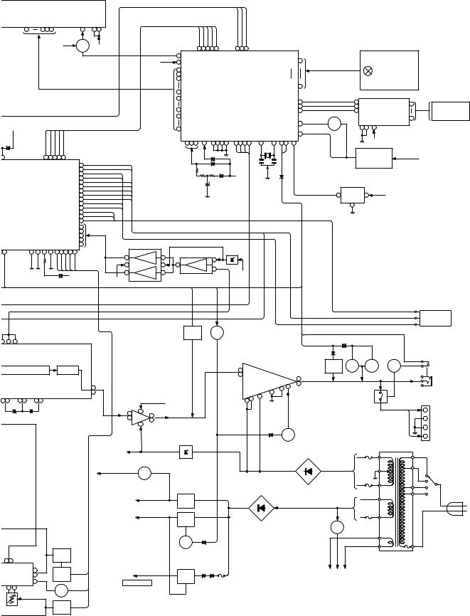
CD-C440W/CP-C440W
|
FL701 |
|
|
|
|
|
|
|
|
|
|
|
|
|
|
|
|
|
||
|
37 |
|
8 |
6 |
5 |
|
|
|
7 |
|
2 |
1 |
|
|
|
|
|
|
|
|
|
|
|
|
|
|
VP |
|
Q701 |
VF1 |
|
|
13 14 15 16 18 |
19 21 22 |
|
|
|
||||
|
|
|
|
|
|
|
|
|
|
|
|
|
|
|
|
|||||
|
|
|
|
|
|
|
|
|
|
|
(AC) |
|
7 |
STBMAIN SCKMAIN SIMAIN |
SOMAIN CLEAR |
MUTETUN SDTUN SMTUN |
|
|
|
|
|
|
|
|
|
|
|
|
|
|
|
|
|
|
5 |
|
|
|
|
|
|
|
|
|
|
|
|
|
|
|
|
|
|
|
VP |
71 |
|
|
|
|
|
|
|
|
|
|
|
|
|
|
|
|
|
|
|
|
6 |
|
|
|
|
|
|
|
|
|
|
|
|
|
|
|
|
|
|
|
|
4 |
|
|
|
|
|
|
|
|
|
|
|
|
|
|
|
|
|
|
|
|
1 |
|
|
IC701I |
|
|
|
|
|
|
|
|
|
|
|
|
|
|
|
|
|
|
X0170AW |
|
|
|||
|
|
|
|
|
|
|
|
|
|
|
|
|
|
|
|
|
|
|||
|
|
|
|
|
|
|
|
|
|
|
|
|
|
80 |
|
MICROCOMPUTER |
|
|||
|
|
|
|
|
|
|
|
|
|
|
|
|
|
|
|
|
||||
|
|
|
|
|
|
|
|
|
|
|
|
|
|
72 |
|
|
|
|
|
|
|
|
|
|
|
|
|
|
|
|
|
|
|
|
70 |
|
|
|
|
|
|
|
+B1 |
|
|
|
|
|
|
|
|
|
|
|
|
54 |
|
|
|
|
|
|
|
|
|
|
|
|
|
|
|
|
|
|
|
|
|
|
|
|
|
|
|
|
|
|
|
|
|
|
|
|
|
|
|
|
|
|
|
|
CE DI DO CLK |
|
|
|
|
|
|
|
|
|
|
|
|
|
|
|
|
|
52 29 8 |
30 |
48 33 31 20 |
12 11 10 |
9 |
35 |
34 |
|
|
|
|
|
|
|
|
|
|
|
|
|
|
+B6 |
+B5 |
|
|
|
|
|
|
|
|
|
|
|
|
|
|
|
|
|
|
|
|
|
|
|
|
|
|
8 |
|
|
14 15 16 17 18 |
|
|
|
|
|
|
|
|
|
|
|
|
|
||||
|
|
|
MAINSCK |
MAINSO |
MAINSI CLEAR |
MAINSTB |
|
4 CD MUTE |
|
|
|
|
+B1 |
|
|
|
||||
|
|
|
|
7 |
CD SL+ |
|
|
|
|
|
|
|
||||||||
|
|
|
|
|
|
|
|
|
5 |
CD RES |
|
|
|
|
|
|
|
|
||
|
|
|
|
|
|
|
|
|
6 CD SL– |
|
|
|
|
|
|
|
|
|||
|
|
|
|
|
|
|
|
|
9 |
CD CQCK |
|
|
|
MEMORY |
|
|
|
|
||
|
|
|
|
|
|
|
|
|
10 |
CD COIN |
|
|
|
|
|
|
|
|||
|
|
|
|
|
|
|
|
|
|
|
|
BACK UP |
|
|
|
|
||||
|
|
|
|
|
|
|
|
|
11 |
CD SQOUT |
|
|
|
|
|
|
|
|
||
|
IC601 |
|
|
|
|
|
|
|
1213 |
CD WRQ |
|
|
|
|
|
|
|
|
||
|
|
|
|
|
|
|
|
CD RWC |
|
|
|
|
|
|
|
|
||||
|
IX0171AW |
|
|
|
|
|
|
|
19 |
CD PUIN |
|
|
|
|
|
|
|
|
||
CROCOMPUTER |
|
|
|
|
21 |
CD DRF |
|
|
|
|
|
|
|
|
||||||
|
|
|
|
CD O/C SW |
|
|
|
|
|
|
|
|
||||||||
|
|
|
|
|
|
|
|
|
53 |
CD D.NO |
|
|
|
|
|
|
|
|
||
|
|
|
|
|
|
|
|
|
54 |
|
|
|
|
|
|
|
|
|||
|
|
|
|
|
|
|
|
|
55 |
CD U/D |
|
|
|
|
|
|
|
|
||
|
SP4CH |
BALANCE |
SRS |
|
P.LDOLBY |
PASSSRS |
3DSRS ASRS |
BSRS INHSRS |
24 |
|
|
|
IC502/503/504 |
OPE AMP. |
|
|
|
|
|
|
|
|
25 |
|
SPE1-5 |
|
|
|
|
|
|||||||||||
|
|
|
|
|
|
|
|
|
26 |
|
OPEAMP. |
|
|
|
|
|
|
|
||
|
|
|
|
|
|
|
|
|
|
|
|
|
|
|
|
|
|
|
||
|
|
|
|
|
|
|
|
|
27 |
|
|
|
|
|
|
|
|
|
|
|
|
|
|
|
|
|
|
|
|
|
|
|
BA4558 |
|
|
|
|
|
|
|
|
|
|
|
|
|
|
|
|
|
28 |
|
|
|
|
|
|
|
|
|
|
|
|
|
|
|
|
|
|
|
|
|
|
|
|
|
|
|
|
|
|
|
|
44 |
66 |
65 |
64 |
|
63 |
61 60 59 58 57 |
|
|
|
|
|
BA4558 |
|
|
|
|
|
|||
|
|
|
|
|
|
IC504(1/2) |
|
|
|
|
|
|||||||||
PROT |
|
|
|
|
|
|
|
|
|
|
|
1 |
2 |
|
|
|
|
|
||
|
|
|
|
|
|
|
|
|
|
|
|
|
IN |
|
|
MUTE |
|
|||
|
|
|
|
|
|
|
|
|
|
|
|
|
|
|
|
8 |
|
|
|
|
|
|
|
|
|
|
|
|
|
|
|
|
4 |
8 |
7 |
|
|
|
|
|
|
|
|
|
|
|
|
|
|
|
|
|
|
7 |
6 |
|
|
6 |
+B3 |
|
|
|
|
|
|
|
|
|
|
|
+B1 |
|
|
|
|
|
|
|
|
|
|||
|
|
|
|
|
|
|
|
|
|
|
–B1 |
|
|
|
SPE |
|
|
CD |
|
|
|
|
|
|
|
|
|
|
|
|
|
|
|
|
|
|
|
|
|||
|
|
|
|
|
|
|
|
|
|
|
Q501 |
Q829 |
POWER ON/STB |
|
|
|
|
|
|
|
|
|
|
|
|
|
Q502 |
|
SWITCHING |
|
|
4 |
30 |
34 |
|
|
|
|
|
|
|
|
MUTE-S |
POWER |
|
|
|
|
IC501 |
|
|
|
|
|
|
|
|
|
|
||||
C75396E |
|
|
|
|
|
|
|
|
|
|
|
|
|||
|
PROCESSOR |
|
|
|
|
|
|
|
|
|
|
|
|||
|
GRAPHIC EQUALIZER |
VOLUME |
|
|
|
|
|
|
L-IN 1 |
IC901 |
|
||||
|
|
|
|
|
|
|
|
|
|
|
|
|
R-IN 18 |
|
|
|
|
|
|
|
|
|
|
IC651 |
|
|
|
|
|
STK488-020 |
|
|
|
|
|
|
|
R 17 |
|
|
|
|
|
POWER AMP. |
|||
|
|
|
|
|
|
BA4558 |
|
|
|
|
|
+B1 |
|
||
|
|
|
|
|
|
L 31 |
|
|
|
|
|
3 |
|||
4 44 |
|
5 43 |
6 42 |
|
|
OPE AMP. |
|
|
|
–B1 |
|
||||
|
|
|
|
|
|
9 |
14 |
|
|||||||
|
|
|
|
|
|
|
|
|
|
|
|
|
|
11 |
|
L R |
|
L R |
L R |
|
|
|
|
|
+B3 |
|
|
|
|
|
|
|
|
|
|
|
|
IN |
L 3 |
8 |
L |
OUT |
|
|
|
|
|
|
|
X-BASS |
|
|
1 |
|
|
|
|
|
|||||
|
|
|
|
|
R 5 |
|
|
|
|
|
|||||
|
|
|
|
|
|
|
7 R |
|
|
|
|
|
|
||
|
|
|
|
|
|
|
|
4 |
|
|
|
|
|
|
|
|
|
|
|
|
|
|
|
|
|
|
VOLTAGE |
|
|
|
|
|
|
|
|
|
|
|
|
|
|
|
REGURATER |
|
|
|
|
|
|
|
|
|
|
–B1 |
|
–15V |
|
|
|
|
|
||
|
|
|
|
|
|
|
|
|
|
|
|
|
|
||
|
|
|
|
|
|
|
|
VOLTAGE |
|
|
|
|
|
|
|
|
|
|
|
|
|
|
|
REGULATOR |
|
|
|
|
|
|
|
|
|
|
|
|
|
+B1 |
+5V |
Q828 |
|
|
|
|
|
|
|
|
|
|
|
|
|
|
|
|
|
|
|
|
|
||
|
|
|
|
|
|
UN-SWITCHED |
|
|
|
|
|
|
|
|
|
|
|
|
|
|
|
|
|
|
|
|
VOLTAGE |
|
|
|
|
|
|
|
|
|
|
|
|
|
|
|
REGULATOR |
|
|
|
|
|
|
|
|
|
|
|
+B2 |
+12V(MOTOR) |
Q826 |
|
|
|
|
||
|
|
|
|
|
|
|
|
|
|
|
|
|
|
||
|
|
|
|
|
|
|
|
|
|
|
Q827 |
|
|
|
|
|
|
|
|
|
|
|
|
|
|
|
VOLTAGE |
|
|
|
|
|
|
|
|
|
|
|
|
|
|
|
REGULATOR |
|
|
|
|
|
|
|
|
|
|
|
+B3 |
+12V(ANALOG) |
Q823 |
|
|
|
|
||
|
|
|
|
|
|
|
|
|
|
|
|
|
|
||
|
|
|
|
|
|
|
|
|
|
|
Q824 |
|
|
D802–D805 |
|
|
|
|
|
|
|
|
|
|
|
|
|
|
|
||
|
|
|
|
|
|
|
|
|
|
|
Q825 |
|
|
|
|
|
|
|
|
|
Q468 |
LEVEL |
|
|
|
|
SWITCHING |
|
|
|
|
UT L-OUT |
|
|
|
|
|
|
|
|
|
|
|||||
|
Q469 |
CONT |
|
|
|
|
|
|
|
|
|
||||
|
17 18 |
|
|
|
|
|
|
|
|
|
VOLTAGE |
|
|
|
|
|
|
|
|
|
|
|
|
|
|
|
|
|
|
|
|
451 |
|
L-IN |
|
|
SRS |
|
|
|
|
REGULATOR |
|
|
|
|
|
|
27 |
Q466 |
PASS |
|
+7.3V(CD) |
|
|
|
|
|
|
||||
5250S |
R-IN 28 |
+B4 |
|
Q821 |
|
|
|
|
|||||||
Q467 |
|
|
|
|
|
|
|||||||||
|
|
|
|
|
|
|
|
||||||||
RS |
|
MODE 26 |
|
SRS |
|
|
|
|
Q822 |
F821 |
|
|
|||
|
|
TO CD UNIT |
|
|
|
T500mA L 250V |
|
|
|||||||
|
25 |
24 |
|
PASS |
|
PASS |
|
|
|
|
|
|
|
|
|
|
SRS STEREO |
Q463 |
/3D |
|
|
|
|
|
|
|
|
|
|||
|
|
|
SRS MONO |
|
SRS A |
|
|
|
|
|
|
|
|
|
|
|
|
|
MODE1-5 |
|
|
|
|
|
|
|
|
|
|
||
|
|
|
Q458 |
/SRS B |
|
|
|
|
|
|
|
|
|
||
|
|
|
MONO |
SRS INH |
|
|
|
|
|
|
|
|
|
||
ENTER CONT |
|
~ |
|
|
|
|
|
|
|
|
|
|
|||
|
IC453(1/2) |
|
Q460 |
|
|
|
|
|
|
|
|
|
|
||
KEY5 |
23 |
|
|
|
KEY MATRIX |
|
|
|
|
|
|
|
|
|
|||
|
|
|
|
|
|
SW701–SW712 |
|
|
|
|
|
|
|
|
SW717,SW719,SW721 |
|
|
|
|
|
|
|
|
SW723–SW726 |
|
|
|
|
|
|
|
|
SW728–SW740 |
|
|
KEY0 |
28 |
|
|
|
|
|
|
|
|
|
37 |
|
DATA |
2 |
IC702 |
16 |
|
|
|
38 |
|
CLOCK |
3 |
|
||
|
|
|
|
LED701–LED711 |
||||
|
|
36 |
|
LCK |
4 |
BU2092F |
|
|
|
|
|
|
|
LED714–LED719 |
|||
|
|
|
RESET |
Q704 |
VSS |
|
||
POWER MUTE-S |
REMOCON |
17 |
VDD |
5 |
|
|||
|
|
|
|
|
|
|||
|
|
|
1 17 |
18 |
|
|
||
|
|
46 |
SYS STOP |
|
|
|
|
|
43 42 |
47 |
|
|
|
|
+B5 |
|
|
|
|
|
|
|
|
|
||
|
|
|
|
|
|
Q705 |
|
|
|
|
|
|
|
|
Q706 |
|
+B4 |
|
|
|
|
|
|
ZD701 |
|
|
|
|
|
|
REMOCON |
|
|
|
|
|
|
|
|
RX701 |
+B5 |
|
|
|
|
|
|
|
2 REMOTE 3 |
|
|
||
|
|
|
|
SENSOR |
|
|
|
|
|
|
|
|
1 |
|
|
|
|
|
|
|
|
|
TO CD UNIT |
||
|
|
RELAY |
|
|
|
|
|
|
|
PROT |
|
|
|
|
|
|
|
Q903 |
Q997 |
Q998 |
Q999 |
|
|
|
|
Q904 |
|
|
|||
|
|
|
|
|
|
|
|
|
10 |
L-OUT |
|
|
|
JA901 |
|
|
13 |
R-OUT |
|
|
|
HEADPHONES |
|
16 |
6 |
|
|
|
|
|
|
MUTE |
|
|
|
|
|
|
|
|
|
|
|
RL901 |
|
|
|
|
|
|
|
|
RELAY |
|
|
|
|
|
|
|
+ L-CH |
|
|
|
|
|
|
|
- |
GND |
SO901 |
|
|
|
|
|
|
||
|
|
|
|
|
- |
|
SPEAKER |
|
|
|
|
|
GND |
TERMINAL |
|
|
|
|
|
|
|
||
|
Q996 |
|
|
|
+ |
R-CH |
|
SWITCHING |
|
|
|
|
|
|
|
|
|
|
|
|
230–240V |
|
|
|
D801 |
|
|
F802 |
|
|
|
|
|
|
T5A L 250V |
220V |
|
|
|
|
|
|
|
|
|
||
|
|
|
|
|
|
|
|
|
|
|
|
|
|
SW801 |
|
|
|
|
|
|
|
VOLTAGE |
|
|
|
|
|
|
|
SELECTOR |
|
|
|
|
|
F803 |
127V |
|
|
|
|
|
|
110V |
|
|
|
|
|
|
|
T5A L 250V |
|
|
|
|
|
|
|
F804 |
|
|
AC 110/127/220/ |
|
|
|
|
|
|
230–240V |
|
|
|
VOLTAGE |
T1.6A L 250V |
|
|
50/60Hz |
|
|
|
REGULATOR Q801 |
|
|
|
|
|
|
|
|
|
|
T.F |
|
|
|
|
|
|
|
T801 |
|
|
|
|
|
|
|
POWER |
|
|
|
|
|
|
|
TRANSFORMER |
|
|
|
|
VF1 VP VF2 |
|
|
|
|
|
|
|
(AC) |
(AC) |
|
|
|
|
Figure 15 BLOCK DIAGRAM (3/3)
– 15 –

CD-C440W/CP-C440W
A
B
C
D
E
F
G
H
|
|
|
|
|
|
|
|
|
|
R1 |
|
|
|
|
|
|
|
|
|
|
|
|
|
|
|
|
|
|
|
|
|
|
|
|
|
|
|
|
|
|
|
|
|
|
|
|
|
|
|
|
|
|
|
|
|
|
|
|
|
|
|
|
|
1K |
|
|
|
|
+B |
|
|
|
|
|
|
|
|
|
|
|
|
|
|
|
|
|
|
|
|
|
|
|
|
|
|
|
|
|
|
|
|
|
|
|
+B |
||
|
|
|
|
|
|
|
|
|
C1 |
|
C2 |
|
|
|
|
|
|
|
|
|
|
|
|
|
|
|
|
|
|
|
|
|
|
|
|
|
|
|
|
|
|
|
|
|
|
|
|
|
|
|
|
|
|
|
|
|
|
|
|
|
|
|
0.01 |
|
47/16 Q1 |
|
C24 |
1/50 |
|
C40 |
0.33/50 |
|
|
C39 |
0.47/50 |
C38 0.01 |
|
|
C37 |
220/10 |
C35 |
0.1/50 |
|
|
|
|
|
|
|
|
|
|
|
|
|
|
|
|
|
||||||||
|
|
|
|
|
|
|
|
|
|
|
KTA1266 GR |
|
|
|
|
|
|
|
|
|
|
|
|
|
|
|
|
|
|
|
|
|
|
|
|||||||||||||||||||
|
|
|
|
|
|
|
|
|
|
|
|
|
|
|
|
|
|
|
|
|
|
|
|
|
|
|
|
|
|
|
|
|
|
|
|
|
|
|
|
|
|
|
|
|
|
|
|
|
|
|
|||
|
|
|
|
|
|
|
|
|
|
C25 |
|
|
R43 |
|
|
|
|
|
|
|
|
|
|
|
|
|
|
|
|
|
|
|
|
|
|
|
|
|
|
|
|
|
|
|
|
|
|
|
|
|
|
|
|
|
|
|
|
|
|
|
|
|
|
0.01 |
|
|
22 |
|
|
|
|
|
|
|
|
|
|
|
|
|
|
|
|
|
|
|
|
|
|
|
|
|
|
|
|
|
|
|
|
|
|
|
|
|
|
|
|
|
|
|
|
|
|
|
|
|
|
+B |
|
|
|
|
|
|
|
|
|
|
R42 560 |
|
|
|
|
|
|
|
|
|
|
|
|
|
|
|
|
|
|
|
|
|
|
|
|
|
|
|
|
|
|
||
|
|
|
CNS1B |
|
|
CNS1A |
CNP1 |
K |
|
|
|
|
|
|
|
|
VCC1 |
|
LDS |
|
PHI |
|
|
|
|
|
LF2 |
VR |
|
|
REF1 |
|
VCC256 |
FSS55 |
DRF |
CE |
|
DAT |
|
50 |
CLK |
DEF |
|
|
R41 4.7K C45 4.7/50 |
|
|
||||||
|
|
|
|
|
|
|
|
|
|
|
FIN2 |
+ |
62 LDO |
BHI |
|
|
|
|
|
|
|
|
52 |
CL |
|
|
|
|
|||||||||||||||||||||||||
|
|
|
|
|
|
|
|
|
|
|
|
|
|
|
|
64 |
63 |
|
|
|
|
61 |
60 |
|
|
|
|
|
59 |
|
58 |
|
|
57 |
|
|
|
|
54 |
53 |
|
51 |
|
49 |
|
|
|
|
|
|
|||
|
|
|
|
|
|
|
|
|
|
|
|
|
|
|
|
|
|
– |
|
|
|
|
|
|
|
|
|
|
|
|
|
|
|
|
|
|
|
|
|
|
|
|
|
|
|
|
|
|
NC 48 |
|
C50 |
||
|
|
F |
1 |
|
|
1 |
1 |
|
|
|
|
|
|
1 |
|
|
|
– |
|
|
RF |
|
|
|
|
|
|
|
|
|
|
|
+ |
|
|
|
|
|
|
|
|
|
|
|
|
|
|
|
|
|
|||
|
|
|
|
A |
|
|
|
|
|
REF |
|
|
|
|
|
|
|
|
|
|
|
|
|
|
|
|
– |
|
|
|
|
|
|
|
|
|
|
|
|
|
|
|
|
|
0.1 |
||||||||
|
|
B |
2 |
|
|
2 |
2 |
|
|
|
|
|
|
|
+ |
|
|
|
|
|
|
|
|
|
|
|
|
REF |
|
|
|
|
|
|
|
|
|
|
|
|
|
|
|
|
TBC 47 |
|
|||||||
|
|
|
|
B |
|
|
|
|
|
2 |
FIN1 |
|
|
|
|
|
|
|
|
|
|
|
|
|
|
|
|
|
|
|
|
|
|
|
|
|
|
|
|
|
|
|
|
|
|||||||||
|
|
K |
3 |
|
|
3 |
3 |
|
|
|
|
|
REF |
|
– |
|
|
|
– |
FE1 |
|
|
|
|
|
|
|
+ |
|
|
|
|
|
|
|
EFBAL |
|
|
|
|
|
|
|
|
|
|
|
|
|||||
|
|
|
|
|
|
|
|
|
|
|
|
|
|
|
|
|
|
|
|
|
|
|
|
– |
|
|
DEF |
|
|
|
|
|
|
|
|
|
|
|
|
|
|
|
|
|
|||||||||
|
|
E |
4 |
|
|
4 |
4 |
E |
|
|
|
|
|
3 |
E |
|
|
+ |
|
|
+ |
REF |
|
|
|
|
|
|
|
– |
|
|
|
|
|
|
|
FOSTA |
|
|
|
FSC |
|
|
|
46 |
|
|
|
||||
|
|
|
|
|
|
|
|
|
|
|
|
|
|
|
|
|
|
|
|
|
|
|
|
|
+ |
|
|
HFL |
|
|
|
|
|
|
|
|
|
|
|
DGND 45 |
|
|
|
||||||||||
|
|
|
|
F |
|
|
|
|
|
F |
|
|
|
|
– |
|
|
VCR |
|
|
|
|
|
|
|
|
|
|
|
|
TOSTA |
|
|
|
|
|
|
|
|
|
|||||||||||||
|
|
K |
5 |
|
|
5 |
5 |
|
|
C3 |
|
|
4 |
|
|
|
REF |
|
|
|
VCR |
|
|
|
|
|
|
|
|
|
|
|
|
|
|
|
|
|
CE |
REF |
|
|
SLI |
44 |
|
|
|
||||||
|
|
|
|
|
|
|
|
|
|
|
+ |
|
|
|
|
|
|
|
|
+ |
|
|
DRF |
|
|
|
2FREQ |
|
|
+ – |
|
|
|
||||||||||||||||||||
|
|
|
|
|
|
|
|
|
|
0.1/50 |
|
5 |
TB |
|
|
|
|
|
|
|
|
|
|
|
|
VCR |
|
– |
|
|
|
|
|
|
|
|
|
CL |
|
|
|
|
|
|
|
C34 |
|
||||||
|
|
|
|
|
|
|
|
|
|
R3 |
|
|
|
|
+ |
|
|
VCR |
+ |
|
|
|
|
LA9240M |
|
LASER |
LATOH |
|
|
|
|
|
SLC |
C33 |
0.001 |
|
|||||||||||||||||
|
|
|
|
|
|
|
|
|
|
C4 0.001 |
|
7 |
TE |
|
|
|
|
|
|
|
|
|
|
|
|
|
8/12CM |
|
|
|
|
|
|
47K |
|
||||||||||||||||||
|
|
|
|
|
|
|
|
|
|
|
|
|
|
|
|
|
|
|
|
|
|
– |
|
|
|
|
|
|
|
|
IC1 |
|
|
|
|
|
|
|
|
|
|
|
|
|
|
|
0.033 |
||||||
|
|
|
|
|
|
|
|
|
|
|
|
R2 |
15K |
6 |
TE– |
|
REF |
– |
|
|
|
|
|
|
|
|
|
|
|
|
|
|
|
|
FSTA |
|
|
|
|
|
|
|
|
|
|
R36 |
|
||||||
|
|
|
|
|
|
|
|
|
|
|
|
100K |
|
|
|
|
|
|
|
|
|
|
|
|
|
|
|
|
|
|
|
|
|
|
|
|
|
|
|
|
|
|
|
|
|
|
|
|
|
|
|
||
|
|
|
|
|
|
|
|
|
|
|
|
TE |
|
|
|
|
REF |
+ |
|
|
|
|
|
+ |
|
|
|
|
SERVO AMP. SLOF |
|
|
|
|
|
|
|
|
43 |
|
|
|
||||||||||||
|
|
|
|
|
|
|
|
|
|
|
|
|
C5 |
|
|
|
|
|
– |
|
|
|
|
|
|
|
|
|
|
|
|
|
|
|
|
|
|
|
|
|
|
|
|
|
|
|
|
|
R33 |
C32 R34 |
|||
|
|
|
|
|
|
|
|
|
|
|
|
|
|
|
|
|
|
|
|
|
|
REF |
|
– |
|
|
|
|
|
|
|
|
VCC |
|
|
|
|
|
|
|
|
|
|
|
|
|
|
|
|||||
|
|
|
|
|
|
|
|
|
|
R4 |
0.033 |
|
TESI |
|
|
|
|
|
|
|
|
|
|
|
|
|
|
|
|
|
+ |
|
|
|
|
|
|
|
|
|
|
|
|
RFS– |
|
5.6K |
27P |
1K |
|||||
|
|
|
|
|
|
|
|
|
|
8 |
|
|
|
|
|
|
|
|
|
|
|
|
|
|
|
|
|
|
|
|
|
|
|
|
|
|
|
|
|
|
42 |
||||||||||||
|
|
|
|
|
|
|
|
|
|
|
C6 |
|
|
|
|
|
|
|
|
|
|
|
|
|
|
|
|
|
|
|
|
|
|
|
|
|
|
|
|
|
|
|
|
|
|||||||||
|
|
|
|
|
|
|
|
|
|
2.2K |
|
|
|
|
|
|
|
|
|
|
|
|
|
|
|
|
|
|
|
|
|
– |
|
|
|
|
|
|
|
|
|
|
REF |
|
|
|
|
C30 2.2P |
|
|
|||
|
|
|
|
|
|
|
|
|
|
6.8K |
|
0.033 |
|
SCI |
|
|
|
|
|
|
|
|
– |
|
|
TGL1 |
|
|
|
|
|
|
|
– |
CV– |
|
|
|
|
+ – |
|
|
56K |
|
|||||||||
|
|
|
|
|
|
|
|
|
|
|
|
|
|
|
|
|
|
|
|
|
|
|
– |
|
|
|
|
|
|
|
|
|
|
|
|
||||||||||||||||||
|
|
|
|
|
|
|
|
|
|
R5 |
|
9 |
|
|
|
|
|
|
|
|
|
|
|
|
|
|
|
|
|
|
|
+ |
|
|
REF |
|
|
|
|
|
|
|
|
|
|
|
R32 |
|
|||||
|
|
|
|
|
|
|
|
|
|
|
|
|
|
|
|
|
|
|
|
|
|
|
|
+ |
|
|
|
|
|
|
|
|
|
|
|
|
|
+ |
|
|
|
|
|
|
|
|
|
|
|
|
|
||
|
|
|
|
|
|
|
|
|
|
|
|
|
|
|
|
|
|
|
|
|
|
|
|
|
|
|
|
|
|
|
|
REF |
|
|
|
|
|
|
CV+ |
|
|
|
RF |
RFSM |
41 |
|
|
|
|||||
|
|
|
|
|
|
|
|
|
|
|
|
|
|
|
|
|
|
|
|
|
|
|
|
|
|
|
|
|
|
|
GL |
S.Q.R |
|
|
|
|
|
|
|
|
|
|
|
|
|
HF |
|
|
|||||
|
|
|
|
|
|
|
|
|
|
|
100 |
0.1/50 |
TH |
|
|
|
|
|
|
|
|
|
|
|
|
|
THDL |
|
|
|
|
|
|
|
+ |
|
|
|
|
|
|
|
|
|
|
470 |
|
||||||
|
|
|
|
|
|
|
|
|
|
|
|
R6 |
C7 |
|
|
|
|
|
REF |
|
|
|
|
|
|
|
|
|
|
THD |
|
|
FSTA |
REF |
|
|
JP– |
|
|
|
|
|
|
|
|
R35 |
|
||||||
|
|
|
|
|
|
|
|
|
|
R7 |
|
C9 |
C8 |
10 |
|
|
|
– |
|
|
|
|
|
|
|
|
|
|
|
|
|
|
|
|
|
|
JP |
|
– |
JP+ |
|
|
|
|
|
CV+ |
40 |
TP1 |
|
|
|||
|
|
|
|
|
|
|
|
|
|
|
|
|
|
|
|
|
|
|
|
|
|
|
|
|
|
|
|
|
|
|
|
|
|
|
|
|
|
|
|
|
|
|
|||||||||||
|
1/16 |
|
|
|
|
|
|
|
|
1K |
0.047 |
0.068 |
|
|
|
|
|
+ |
|
|
|
|
|
|
|
|
|
|
|
|
|
|
|
|
|
|
|
|
JPCLO |
|
|
|
|
|
|
39 |
|
|
|
||||
LD |
|
|
|
|
|
|
|
|
|
|
|
|
11 |
|
|
|
|
|
|
|
|
|
JP |
|
|
FSC |
|
|
|
|
|
|
|
|
|
|
|
SLOF SLOF |
|
|
|
|
|
CV– |
|
|
|
||||||
MON |
|
|
|
|
|
|
|
|
|
|
|
|
12 |
|
|
|
GEN |
|
+ |
|
|
|
|
|
|
REF |
|
|
|
|
|
|
|
|
|
|
SLOF |
38 |
|
|
|
||||||||||||
|
|
|
|
|
|
|
|
|
|
|
|
|
TD– |
|
|
REF |
FOSTA |
|
REF |
|
FE1 |
|
|
– |
|
|
|
|
|
OR |
|
|
|
|
|
|
|||||||||||||||||
K |
|
|
|
|
|
|
|
|
R9 |
|
|
R8 |
|
|
|
|
|
|
– |
|
GEN |
|
|
|
|
|
+ |
|
|
|
|
|
|
|
|
|
|
|
|
|
|
|
|||||||||||
|
|
|
|
|
|
|
|
|
|
|
|
|
|
|
|
|
|
|
|
TO |
|
|
|
+ |
|
|
|
|
|
|
|
|
|
|
|
|
|
|
SLOF |
|
|
|
HFL |
37 |
|
|
|
||||||
B |
|
|
|
|
|
|
|
|
|
27K |
R11 |
12K |
13 |
TD |
|
|
REF |
|
REF+ |
|
|
GEN |
|
– |
REF |
|
– |
|
|
|
+ |
– |
|
|
|
|
REF |
|
|
+ |
|
|
|
|
TES |
36 |
|
|
|
||||
|
|
|
|
|
|
|
|
|
|
|
|
|
|
|
|
|
|
|
|
|
|
|
|
|
|
|
|
|
– |
|
|
|
|
|
|
|
|||||||||||||||||
E |
|
|
|
|
|
|
|
|
|
|
|
|
|
|
|
|
|
|
|
|
|
|
|
|
|
+ |
|
|
|
|
|
|
|
|
|
|
|
|
|
|
|
|
|
|
|
|
|||||||
|
LD GND |
|
5 |
K |
|
|
|
|
|
|
|
3.3K |
C10 |
14 |
JP |
|
|
|
|
– |
|
REF |
|
|
|
|
|
|
|
|
|
|
|
|
|
|
|
|
|
|
|
|
|
|
|
TOFF |
35 |
|
|
|
|||
|
|
|
|
|
|
|
|
|
|
180P |
|
+ |
|
– |
|
|
|
+ |
|
|
|
|
|
|
|
|
|
|
|
|
|
|
|
|
|
|
|
|
|
|
+ |
|
|
|
|
|
|
|
|||||
A |
|
|
4 |
E |
|
|
|
|
|
|
|
|
|
15 TO |
|
|
|
|
|
|
– |
|
|
|
|
|
|
|
|
|
|
|
|
|
|
|
|
|
|
|
|
|
|
– |
|
|
TGL |
34 |
|
|
|
||
F |
|
|
|
|
|
|
|
|
|
|
|
16 FD |
|
|
|
|
|
|
|
|
|
|
|
|
|
|
|
|
|
|
|
|
|
|
|
SLEO |
|
|
|
|
|
|
|
JP+ |
|
|
|
|
|||||
|
|
3 |
A |
|
|
|
|
|
|
|
|
|
|
|
|
|
|
|
|
FA– |
|
|
|
|
|
AGND |
|
|
REF |
SPI SPG |
SP– |
|
|
SPO |
|
|
|
SLD |
SL– |
|
SL+ |
33 |
|
|
|
||||||||
C |
2200P |
|
|
|
|
|
|
|
|
|
|
|
|
|
FD– |
|
FA |
|
FE |
|
FE– |
|
SP |
|
|
|
|
REF |
|
|
JP– |
|
|
|
|
|
|||||||||||||||||
|
|
|
2 |
B |
|
|
|
|
|
|
|
|
R13 |
|
|
|
|
17 |
|
18 |
19 |
20 |
|
21 |
|
22 |
23 |
|
24 |
25 26 |
|
|
27 |
|
28 |
|
|
|
29 |
30 |
31 |
32 |
|
|
|
|
|||||||
|
|
|
1 |
F |
|
|
|
|
|
|
|
|
33K |
|
|
|
|
|
|
|
|
C120.01 |
|
|
|
|
|
|
|
R2010K |
R2156K |
|
|
|
|
|
|
|
|
|
|
|
|
|
|
|
|
|
|
||||
FO+ |
|
|
2 |
T+ |
|
|
|
|
|
|
|
1K |
1K |
|
15K |
|
|
R14 10K |
|
|
|
|
C15 |
0.0047 |
|
|
|
|
|
C19 |
|
R24 10K |
|
|
|
|
|
|
|
|
|
|
|||||||||||
LT0H30M1 |
1M |
|
|
|
|
|
|
|
|
|
|
|
0.1 |
|
|
|
|
|
|
330P |
R17 |
82K |
|
|
|
|
|
|
|
|
C16 R22 |
0.001 6.8K |
|
R25 1.2K47/16 |
C18 |
1/50 |
|
|
|
|
|
|
|
|
|
|
|||||||
|
2200P |
|
5 |
|
|
|
|
|
|
R40 22K |
|
|
C13 |
R12 |
|
|
|
|
|
|
|
|
|
|
|
|
|
|
|
|
|
|
22K |
C20 |
0.0033 |
|
R26 |
220K |
R27 |
220K |
|
|
|||||||||||
TR+ |
1M |
|
1 |
T– |
|
|
|
|
|
|
|
R28 |
R29 |
|
|
|
|
|
|
|
|
|
|
C14 |
|
|
|
|
|
|
|
|
|
|
|
|
|
|
|
|
|
|
|
|
|
|
|
|
|
|
|
||
|
|
|
|
|
|
|
|
|
|
|
|
|
|
|
|
|
|
|
|
|
|
|
|
|
|
|
|
|
|
|
|
|
|
|
|
|
|
|
|
|
|
|
|
|
|
|
|
||||||
|
|
|
|
|
|
|
|
|
|
|
|
|
|
|
|
|
|
|
|
|
|
|
|
|
|
|
|
|
|
|
|
|
|
|
|
|
|
|
|
|
|
|
|
|
|
|
|
|
|||||
|
|
|
3 |
F+ |
|
|
|
|
|
|
|
R39 |
|
|
|
|
|
|
|
R15 |
|
R16 |
|
|
|
|
|
R19 |
|
R23 |
|
|
|
|
|
|
|
|
|
|
|
|
|
|
|
|
|
|
|||||
|
|
|
4 |
F– |
|
|
|
|
|
|
|
|
|
|
|
|
|
|
|
|
|
|
|
|
39K |
|
1.2K |
|
|
|
|
|
|
|
|
|
|
|
|
|
|
|
|
|
|
||||||||
FO– |
|
|
|
|
|
|
|
|
|
|
22K |
|
|
|
|
|
|
|
47K |
|
1.5K |
|
|
|
|
|
|
|
|
|
|
|
|
|
|
|
|
R30 |
|
|
|
|
|
|
|
|
|
||||||
|
|
|
GND |
|
|
|
|
|
|
|
|
|
|
|
|
|
|
|
|
|
|
|
|
|
|
|
|
|
|
|
|
|
|
|
|
|
|
|
|
|
|
|
|
|
|
|
|
|
|||||
|
|
|
|
|
|
|
|
|
|
|
|
VREF |
|
|
|
|
|
|
|
|
|
|
|
|
|
|
|
|
|
|
|
|
|
|
|
|
|
|
|
|
|
|
|
|
|
|
|
|
|
||||
TR– |
|
|
6 |
PD |
|
|
|
|
|
|
|
|
|
|
|
|
|
|
|
|
|
|
|
|
|
|
|
|
|
|
|
|
|
|
|
+B |
|
|
|
|
|
|
|
|
|
|
|
|
|
||||
|
|
|
|
|
|
|
|
C11 |
|
|
|
|
|
|
|
|
|
|
|
|
|
|
|
|
|
|
|
|
|
|
|
C17 |
|
|
|
|
|
|
|
|
|
|
|
|
|
|
|
||||||
ACTUATOR |
|
|
7 |
VR |
|
|
|
|
|
|
|
|
|
|
|
|
|
|
|
|
|
|
|
|
|
|
|
|
|
|
|
|
|
|
|
|
|
|
|
|
|
|
|
|
|
|
|
||||||
|
|
|
|
|
|
|
0.1 |
|
|
|
|
|
|
|
|
|
|
|
|
|
|
|
|
|
|
|
|
|
|
|
0.47/50 |
|
|
|
|
|
|
|
|
|
|
|
|
GND |
|
||||||||
|
|
|
LD |
|
|
|
|
|
|
|
|
|
|
|
|
|
|
|
|
|
|
|
|
|
|
|
|
|
|
|
|
|
|
|
|
|
|
|
|
|
|
|
|
|
|||||||||
|
|
|
8 |
|
|
|
|
|
|
|
|
|
|
|
|
|
|
|
|
|
|
|
|
|
|
|
|
|
|
|
|
|
|
|
|
|
|
|
|
|
|
|
|
|
|
|
|
|
|
|
|||
|
|
|
|
|
|
|
|
|
|
|
|
|
|
|
|
|
|
|
|
|
|
|
|
|
|
|
|
|
|
|
|
|
|
|
|
|
|
|
|
|
|
|
|
|
|
|
|
|
|
C21 |
|||
|
|
|
|
|
|
|
|
|
|
|
|
|
|
|
|
|
|
|
|
|
|
|
|
|
|
|
|
|
|
|
|
|
|
|
|
|
|
|
|
|
|
|
|
|
|
|
|
|
|
|
|
||
|
|
|
|
|
|
|
|
|
|
|
|
|
|
|
|
|
|
|
|
|
|
|
|
|
|
|
|
|
|
|
|
|
|
|
|
|
|
|
|
|
|
|
|
|
|
|
|
|
|
|
|
1/50 |
|
PICKUP UNIT |
|
|
|
|
|
|
|
|
|
|
|
|
|
|
|
|
|
|
|
|
|
|
|
|
|
|
|
|
|
|
|
|
|
|
|
|
|
|
|
|
|
|
|
|
|
|
|
|
R10 |
|
|
||
|
|
|
|
|
|
|
|
|
|
|
|
|
|
|
|
|
|
|
|
|
|
|
|
|
|
|
|
|
|
|
|
|
|
|
|
|
|
|
|
|
|
|
|
|
|
|
|
82K |
|
1S |
|||
|
|
|
|
|
|
|
|
|
|
|
|
|
|
|
|
|
|
|
|
|
|
|
|
|
|
|
|
|
|
|
|
|
|
|
|
|
|
|
|
|
|
|
|
|
|
|
|
|
|
|
|
||
|
|
|
|
|
|
|
|
|
|
|
|
+B |
|
|
1 |
|
|
|
|
|
|
|
|
|
|
|
|
|
36 |
|
|
|
|
|
|
|
|
|
|
|
|
|
|
|
|
|
|
|
|
|
|
|
|
|
|
|
|
|
|
|
|
|
|
|
|
|
|
2 |
|
|
|
|
|
|
|
|
|
|
|
|
|
35 |
|
|
|
|
|
|
|
|
|
|
|
|
|
|
|
|
|
|
|
|
|
|
|
||
|
|
|
|
|
|
|
|
|
|
|
|
|
|
|
|
|
|
|
|
|
|
|
|
|
|
|
|
|
|
|
|
|
|
|
|
|
|
|
|
|
|
|
|
|
|
|
|
+B |
|
|
|||
|
|
|
|
|
|
|
|
|
PD |
|
|
|
|
|
3 |
|
|
|
|
|
|
|
|
|
|
|
|
|
34 |
|
|
|
|
|
|
|
|
|
|
|
|
|
|
|
|
|
|
|
|
|
|
||
|
|
|
|
|
|
|
|
|
|
|
|
|
|
|
|
|
|
|
|
|
|
|
|
|
|
|
|
|
|
|
|
|
|
|
|
|
|
|
|
|
|
|
|
|
|
|
|
|
D |
||||
|
|
|
|
CNS2B |
CNS2A |
|
|
|
|
|
|
|
4 |
|
|
|
|
|
|
|
FOCUS/TRACKING/SPIN/ |
|
|
|
|
|
33 |
|
|
|
|
|
|
|
|
|
|
|
|
|
|
|
|
|
|
|
|
|
|
||||
|
|
|
|
|
CNP2 |
|
|
|
|
|
|
|
|
|
|
|
|
|
|
|
|
|
|
|
|
|
|
|
|
|
|
|
|
|
|
|
|
|
|
|
|
|
|
RL10 |
|||||||||
|
|
|
|
|
|
|
|
C44 |
|
15 |
|
|
|
IC5 |
M56748FP |
DRIVERSLIDE |
|
|
|
|
22 |
10K |
|
|
|
|
|
|
|
|
|
|
|
|
|
|
|
|
|
|
|
||||||||||||
|
|
|
|
|
|
|
|
|
|
|
|
|
|
|
5 |
|
|
|
|
|
|
|
|
|
|
|
|
|
32 |
|
|
|
|
|
|
|
|
|
|
|
|
|
|
|
|
|
|
|
|
|
|
|
|
|
|
|
|
|
|
|
|
|
|
TR– |
|
|
|
|
6 |
|
|
|
|
|
|
|
|
|
|
|
|
|
31 |
|
|
|
|
|
|
|
|
|
|
|
|
|
|
|
|
|
|
|
|
|
|
|
|
|
|
|
TR– |
1 |
1 |
TR– |
1 |
|
|
|
|
|
7 |
|
|
|
|
|
|
|
|
|
|
|
|
|
30 |
|
|
|
|
|
|
|
|
|
|
|
|
|
|
|
|
|
|
|
|
|
|
|
|||
|
|
|
|
TR+ |
|
|
|
|
|
|
|
|
|
|
|
|
|
|
|
|
|
|
|
|
|
|
|
|
|
|
|
|
|
|
|
|
|
|
|
|
|
D6 |
|
||||||||||
|
|
|
TR+ |
|
2 |
2 |
TR+ |
2 |
|
|
|
|
|
8 |
|
|
|
|
|
|
|
|
|
|
|
|
|
29 |
|
|
|
|
|
|
|
|
|
|
|
|
|
|
|
|
|
|
|
|
|
||||
|
|
|
FO+ |
|
3 |
3 |
FO+ |
3 |
|
FO+ |
|
|
|
|
9 |
|
|
|
|
|
|
|
|
|
|
|
|
|
28 |
|
|
|
|
|
|
|
|
|
|
|
|
|
|
|
|
|
|
|
|
RL104A |
|
||
|
|
|
|
|
FO– |
|
|
|
|
|
|
|
|
|
|
|
|
|
|
|
|
|
|
|
|
|
|
|
|
|
|
|
|
|
|
|
|
|
|
|
|
|
|
|
|
||||||||
|
|
|
FO– |
4 |
4 |
FO– |
4 |
|
|
|
|
|
10 |
|
|
|
|
|
|
|
|
|
|
|
|
|
27 |
|
|
|
|
|
|
|
|
|
|
|
|
|
|
|
|
|
|
|
|
|
|
|
|||
|
|
|
|
|
|
|
|
|
|
|
|
|
|
|
|
|
|
|
|
|
|
|
|
|
|
|
|
|
|
|
|
|
|
|
|
|
|
|
|
|
|
|
|
|
|||||||||
|
|
|
GND |
|
5 |
5 |
GND |
5 |
|
|
|
|
|
|
11 |
|
|
|
|
|
|
|
|
|
|
|
|
|
26 |
|
|
|
|
|
|
|
|
|
|
|
|
|
|
|
|
|
|
|
|
|
|
|
|
|
|
|
PD |
|
6 |
6 |
PD |
6 |
|
|
|
|
|
|
12 |
|
|
|
|
|
|
|
|
|
|
|
|
|
25 |
|
|
|
|
|
|
|
|
|
|
|
|
|
|
|
|
|
|
|
|
D5 |
|
||
|
|
|
VR |
|
7 |
7 |
VR |
7 |
|
|
|
|
|
|
13 |
|
|
|
|
|
|
|
|
|
|
|
|
|
24 |
|
|
|
|
|
|
|
|
|
|
|
|
|
|
|
|
|
|
|
|
RL104A |
|||
|
|
|
LD |
|
8 |
8 |
LD |
8 |
LD |
|
|
|
|
|
14 |
|
|
|
|
|
|
|
|
|
|
|
|
|
23 |
R31 |
|
|
|
|
|
|
|
|
|
|
|
|
|
|
|
|
|
|
|
|
|
||
|
|
|
|
|
|
|
|
|
|
|
|
|
|
|
|
|
|
|
|
|
|
|
|
|
|
|
|
|
|
|
|
|
|
|
|
|
|
|
|
|
|
|
|
|
|
|
|
|
|
|
|||
|
|
|
|
|
|
|
|
|
|
|
|
|
100/16 |
|
16 |
|
|
|
|
|
|
|
|
|
|
|
|
|
21 |
|
|
|
|
|
|
|
|
|
|
|
|
|
|
|
|
|
|
|
|
|
|
|
|
|
|
|
|
|
|
|
|
|
|
|
|
|
|
|
17 |
|
|
|
|
|
|
|
|
|
|
|
|
|
20 |
|
|
|
|
|
|
|
|
|
|
|
|
|
|
|
|
|
|
|
|
|
|
|
|
|
|
|
|
|
|
|
|
|
GND |
|
|
|
|
|
18 |
|
|
|
|
|
|
|
|
|
|
|
|
|
19 |
|
|
|
|
|
|
|
|
|
|
|
|
|
|
|
|
|
|
|
|
|
|
|
|
|
|
|
|
|
|
|
|
|
|
|
|
+B |
|
|
|
|
|
|
|
|
|
|
|
|
|
|
|
|
|
|
|
|
|
|
|
|
|
|
|
|
|
|
|
|
|
|
|
|
|
+B |
|
|
|
|
|
|
|
|
|
|
|
|
_ |
|
|
|
|
|
|
|
|
|
|
|
|
|
|
|
|
|
|
|
|
|
|
|
|
|
|
|
|
|
|
|
|
|
|
|
|
|
|
|
|
|
|
|
|
|
|
|
|
|
|
|
|
|
CD |
|
|
|
|
|
|
|
|
|
|
|
|
|
|
|
|
|
|
|
|
|
|
|
|
|
|
|
|
|
|
|
|
|
|
|
|
|
|
|
|
|
|
|
|
|
M1 |
M |
|
|
CNP3A |
CNS3B |
CNS3A |
|
SP+ |
|
|
|
|
|
|
|
|
|
|
|
|
|
|
|
|
|
|
|
|
|
|
|
|
|
|
|
|
|
|
|
|
|
|
|
|
|
|
|
|
|
|
|
|
|
SPINDLE |
|
|
6 |
6 |
6 |
|
|
|
|
|
|
|
|
|
|
|
|
|
|
|
|
|
|
|
|
|
|
|
|
|
|
|
|
|
|
|
|
|
|
|
|
|
|
|
|
|
|
|
|
|||
|
MOTOR |
|
|
|
|
|
SP– |
|
|
|
|
|
|
|
|
|
|
|
|
|
|
|
|
|
|
|
|
|
|
|
|
|
|
|
|
|
|
|
|
|
|
|
|
|
|
|
|
|
|
|
|||
|
|
|
|
|
|
5 |
5 |
5 |
|
|
|
|
|
|
|
|
|
|
|
|
|
|
|
|
|
|
|
|
|
|
|
|
|
|
|
|
|
|
|
|
|
|
|
|
|
|
|
|
|
|
|
|
|
|
|
|
|
|
|
|
SL_+ |
|
|
|
|
|
|
|
|
|
|
|
|
|
|
|
|
|
|
|
|
|
|
|
|
|
|
|
|
|
|
|
|
|
|
|
|
|
|
|
|
|
|
||||
|
M2 |
M |
|
|
4 |
4 |
4 |
|
|
|
|
|
|
|
|
|
|
|
|
|
|
|
|
|
|
|
|
|
|
|
|
|
|
|
|
|
|
|
|
|
|
|
|
|
|
|
|
|
|
|
|||
|
|
|
|
|
|
|
|
|
|
|
|
|
|
|
|
|
|
|
|
|
|
|
|
|
|
|
|
|
|
|
|
|
|
|
|
|
|
|
|
|
|
|
|
|
|
|
|
||||||
|
MOTORSLED |
|
|
3 |
3 |
3 |
|
SL_– |
|
|
|
|
|
|
|
|
|
|
|
|
|
|
|
|
|
|
|
|
|
|
|
|
|
|
|
|
|
|
|
|
|
|
|
|
|
|
|
CD_PUIN |
|||||
|
SW4 |
|
|
|
|
2 |
2 |
2 |
|
CD_PUIN |
|
|
|
|
|
|
|
|
|
|
|
|
|
|
|
|
|
|
|
|
|
|
|
|
|
|
|
|
|
|
|
|
|
|
|
|
|
|
|||||
|
|
|
|
|
|
|
|
|
|
|
|
|
|
|
|
|
|
|
|
|
|
|
|
|
|
|
|
|
|
|
|
|
|
|
|
|
|
|
|
|
|
|
|
|
|
|
|
|
|
|
|
|
|
|
PICKUP |
|
|
|
|
1 |
1 |
1 |
|
|
|
|
|
|
|
|
|
|
|
|
|
|
|
|
|
|
|
|
|
|
|
|
|
|
|
|
|
|
|
|
|
|
|
|
|
|
|
|
|
|
|
|
|
|
IN |
|
|
|
|
|
|
|
|
|
|
|
|
|
|
|
|
|
|
|
|
|
|
|
|
|
|
|
|
|
|
|
|
|
|
|
|
|
|
|
|
|
|
|
|
|
|
|
|
|
|
|
|
|
CD MOTOR PWB-E |
|
|
|
|
|
|
|
|
|
|
|
|
|
|
|
|
|
|
|
|
|
|
|
|
|
|
|
|
|
|
|
|
|
|
|
|
|
|
|
|
|
|
|
|
|
|
|
21 |
||||
|
|
|
|
|
|
|
|
|
|
|
|
|
|
|
|
|
|
|
|
|
|
|
|
|
|
|
|
|
|
|
|
|
|
|
|
|
|
|
|
|
|
|
|
|
|
|
|
|
|
|
|
|
|
• NOTES ON SCHEMATIC DIAGRAM can be found on page 12.
1 |
2 |
3 |
4 |
5 |
6 |
Figure 16 SCHEMATIC DIAGRAM (1/14)
– 16 –
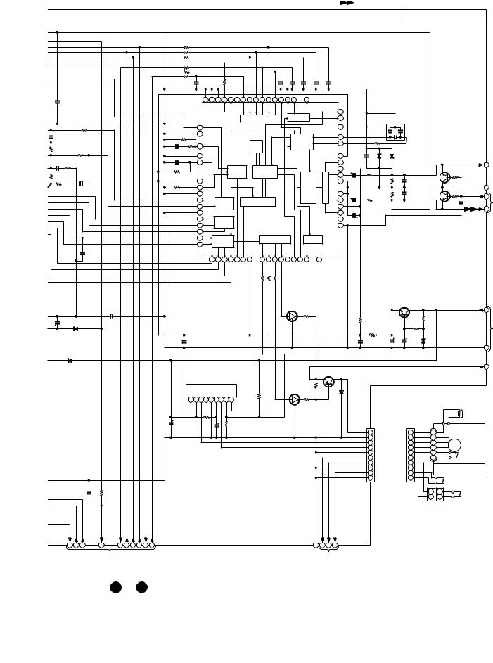
CD-C440W/CP-C440W
CD SIGNAL
MAIN PWB-A1(1/3)
|
|
+B |
|
|
|
|
|
|
|
|
|
|
|
|
|
|
|
|
|
|
|
|
|
|
|
|
|
|
|
|
|
|
|
|
|
|
|
|
|
|
|
|
|
|
+B |
|
|
|
|
|
|
|
|
|
|
|
|
|
|
|
|
|
|
|
R77 |
1K |
|
|
|
|
|
|
|
|
|
|
|
|
|
|
|
|
|
|
|
|
|
|
|
|
|
|
|
|
|
|
|
|
|
|
|
|
|
|
|
|
|
|
|
|
|
|
|
|
|
R46 |
1K |
|
|
|
|
|
|
|
|
|
|
|
|
|
|
|
|
|
|
|
|
|
|
|
|
|
|
|
|
|
|
|
|
|
|
|
|
|
|
|
|
|
|
|
|
|
|
|
|
|
R47 |
1K |
|
|
|
|
|
|
|
|
|
|
|
|
|
|
|
|
|
|
|
|
|
|
|
|
|
|
|
|
|
|
|
|
|
|
|
|
|
|
|
|
|
|
|
|
|
|
|
|
|
R45 |
1K |
|
|
|
|
|
|
|
|
|
|
|
|
|
|
|
|
|
|
|
|
|
|
|
|
|
|
|
|
|
|
|
|
|
|
|
|
|
|
|
|
|
|
|
|
|
|
|
|
|
R78 |
1K |
|
|
|
|
|
|
|
|
|
|
|
|
|
C54 |
100P |
C55 100P |
C57 100P |
C58 100P |
C56 100P |
|
|
|
|
|
|
|
|
|
|
|
|
||||
|
|
|
|
|
|
|
|
|
|
|
|
|
|
R48 |
1K |
|
|
|
|
|
|
|
|
|
|
|
|
|
|
|
|
|
|
|
|
|
|
|
|
|
||||||||||
|
|
|
|
|
|
|
|
|
|
|
|
|
|
|
|
C22 |
|
|
|
R60 |
|
|
|
|
|
|
|
|
|
|
|
|
|
|
|
|
|
|
||||||||||||
|
|
|
|
|
|
|
|
|
|
|
|
|
|
|
|
|
|
|
|
|
|
|
|
|
|
|
|
|
|
|
|
|
|
|
|
|
|
|
|
|
|
|
|
|
|
|
||||
|
4.7/50 |
|
|
|
|
|
|
|
|
|
|
|
|
|
|
0.01 |
|
|
|
1K |
|
|
|
|
|
|
|
|
|
|
|
|
|
|
|
|
|
|
|
|
|
|
|
|
|
|
|
|
|
|
C45 |
|
|
|
|
|
|
|
|
|
|
|
+B |
|
|
|
|
|
|
|
|
|
|
|
|
|
|
|
|
|
|
|
|
|
|
|
|
|
|
+B |
|
|
|
|
|
|
|
|
|
|
|
|
|
|
|
|
|
|
|
|
|
|
|
|
|
|
|
|
|
|
|
|
|
|
|
|
|
|
|
|
|
|
|
|
|
|
|
|
|
|
|
|
|
|
|
|
|
|
|
|||
C50 |
|
|
|
|
|
|
|
|
|
|
|
|
|
64 |
63 |
62 |
61 |
60 |
59 |
58 |
57 |
56 |
55 |
54 |
53 |
52 |
|
51 |
50 |
|
49 |
|
|
|
|
|
|
|
|
|
|
|
|
|
|
|
|
|||
|
|
0.1 |
|
|
|
|
|
|
|
|
|
|
|
|
|
TEST1 |
/CS |
TEST5 |
4M |
16M |
TEST11 |
/RES |
/CQCK |
COIN |
SQOUT |
RWC |
WRQ |
FSX |
SBCK |
SFSY |
|
PW |
|
|
|
|
|
|
|
|
|
|
|
|
|
|
|
|
||
|
|
|
|
|
|
|
|
|
|
|
|
|
|
|
|
|
|
|
EFLG |
48 |
|
|
|
|
|
|
|
|
|
|
|
|||||||||||||||||||
|
|
|
|
|
|
|
|
|
|
|
|
|
|
|
|
|
|
|
SBSY |
47 |
|
|
|
|
|
|
|
|
|
|
|
|||||||||||||||||||
|
|
|
|
|
|
|
|
|
|
|
|
|
|
|
|
|
|
|
|
|
|
|
|
|
-COM |
|
|
|
|
SUB-CODE |
|
|
|
|
|
|
|
|
|
|
|
|
||||||||
|
|
|
|
|
|
|
|
|
|
|
|
|
|
|
|
|
|
|
|
|
|
|
|
INTERFACE |
|
|
|
|
|
|
|
|
|
|
|
|
|
|
|
|
|
|
|
|
|
|
|
|||
|
|
|
|
|
|
|
|
|
|
|
|
|
|
R18 |
|
1 DEF1 |
|
|
|
|
|
|
|
|
|
|
|
|
|
|
|
|
|
XVSS 46 |
|
|
XL10 |
|
|
|
|
|
|
|
|
|||||
|
|
C34 |
|
|
|
R38 |
|
|
|
|
|
|
|
|
2 TA1 |
|
|
|
|
|
|
|
|
|
|
|
|
|
|
|
|
|
|
|
|
XIN |
|
|
R61 |
|
|
|
|
|
|
|
|
|||
|
|
|
|
|
|
|
|
|
|
|
|
3.3M |
|
|
|
|
|
|
|
|
|
|
|
|
|
|
|
|
|
|
|
|
|
45 |
|
|
|
|
|
|
|
|
|
|||||||
|
|
|
|
|
33K |
|
|
|
|
|
|
|
|
|
|
|
|
|
|
|
|
|
|
|
|
|
|
|
|
X-TAL |
|
|
|
|
220 |
|
|
|
|
|
|
|
|
|||||||
|
|
0.033 |
|
|
|
|
|
|
|
|
|
|
|
|
|
|
|
|
|
|
|
|
|
|
|
|
|
|
|
|
|
XOUT |
|
|
|
|
|
|
|
|
|
|
||||||||
|
|
R36 |
|
|
R37 |
|
|
|
|
|
|
|
|
|
3 |
PDO |
|
|
|
|
|
|
2KX8 |
|
|
|
|
|
GENERATOR |
|
44 |
|
|
|
|
|
|
|
|
|
|
|
||||||||
|
|
|
|
|
|
|
|
|
|
|
C41 |
R58 |
|
|
|
|
|
|
|
|
RAM |
|
|
|
|
|
|
|
|
|
|
|
|
|
|
|
|
|
1SS133 |
|
|
|
|
|
|
|||||
|
|
47K |
|
|
47K |
|
|
|
|
|
|
|
|
|
|
|
|
|
|
|
|
|
|
|
|
|
|
|
|
|
|
|
|
|
|
|
C92 0.022 |
D8 1SS133 |
|
|
|
|
|
|
|
|||||
|
|
|
|
|
|
|
|
|
|
|
0.047 |
680 |
4 VVSS |
|
|
|
|
|
|
|
|
|
|
|
|
|
|
|
|
|
XVDD 43 |
D9 |
|
|
|
|
|
|
||||||||||||
|
|
|
|
|
|
|
|
|
|
|
|
|
|
|
|
|
|
|
|
|
|
|
|
|
|
|
|
|
|
|
|
|
|
|
|
|
||||||||||||||
3 |
|
C32 |
R34 |
|
|
|
|
|
|
|
|
|
|
|
|
|
|
|
|
|
|
|
|
|
|
|
|
|
|
|
|
|
|
|
|
|
|
|
||||||||||||
|
|
|
|
|
|
|
|
|
|
|
C42 |
5 |
ISET |
|
|
|
|
|
|
|
|
|
|
|
|
|
|
|
|
|
MUTER |
42 |
|
|
Q84 |
|
1 |
TO MAIN |
||||||||||||
K |
27P |
1K |
|
|
|
|
|
|
|
|
|
|
|
|
|
|
|
|
VCO |
|
|
ERROR |
|
|
|
|
|
|
|
|
|
|
|
|
+B |
|
|
|
|
|
|
KTC3199 GR |
SECTION |
|||||||
|
|
|
|
|
|
|
|
|
|
|
|
|
|
0.047 |
|
|
|
|
|
|
|
|
|
|
|
|
|
|
|
|
|
RVDD |
41 |
|
|
|
|
|
|
|
||||||||||
|
|
|
|
|
|
|
|
|
|
|
|
|
|
|
|
|
|
|
CLOCK |
|
COERECT |
|
|
|
|
|
|
|
|
|
|
|
|
|
CD_R-CH |
|
|
|
P21 9-A |
|||||||||||
|
|
|
|
|
|
|
|
|
|
|
|
|
|
|
|
|
|
|
|
|
|
|
|
|
|
|
|
|
|
RCHO |
|
|
|
|
|
|
|
|
|
|||||||||||
|
|
R32 |
|
|
|
|
|
|
|
|
|
|
+B |
R57 |
|
|
|
|
|
|
OSC |
|
|
FLAG |
|
|
|
|
|
|
|
|
|
40 |
|
|
|
|
|
|
|
|
||||||||
|
|
|
|
|
|
|
|
|
|
|
|
|
|
|
|
|
CONTROL |
CONTROL |
|
|
|
|
|
|
|
|
|
|
|
|
|
|
|
C70 |
|
|
|
|
|
|||||||||||
. |
|
56K |
|
|
|
|
|
|
|
|
|
|
27K |
|
|
|
|
|
|
|
|
|
|
|
|
|
|
|
|
C68 |
R74 |
R76 |
|
|
|
R80 |
|
|
|
|||||||||||
|
|
|
|
|
|
|
|
|
|
|
6 |
VVDD |
|
|
|
|
|
|
|
|
|
|
|
|
|
|
|
|
|
|
RVSS |
39 |
|
|
|
|
|
|
||||||||||||
|
|
|
|
|
|
|
|
|
|
|
|
|
|
|
|
|
|
|
|
|
|
|
|
|
|
|
|
|
|
|
|
1BIT DAC |
2.7K |
390 |
|
|
220P |
|
|
|
|
|||||||||
|
|
R35 |
|
|
|
|
|
|
|
|
|
|
|
|
7 |
FR |
|
|
|
|
|
|
|
|
|
|
|
|
|
|
|
|
4FS DIGITAL FILTER |
|
|
|
|
10/50 |
|
|
A_GND |
4.7K |
|
|
TO DECK |
|||||
|
|
|
|
|
C31 |
|
|
|
|
|
|
|
|
|
|
|
|
|
|
|
|
|
|
|
|
|
|
|
|
|
|
|
|
|
|
|
|
|
2 |
|||||||||||
1 |
|
|
|
|
|
|
|
|
|
|
R56 |
|
VSS |
|
|
|
|
|
|
|
|
|
|
|
|
|
|
|
|
|
|
|
C67 |
|
R75 |
|
|
C69 |
|
|
|
SECTION |
||||||||
|
470 |
|
|
|
0.0027 |
|
|
|
|
|
|
|
8 |
|
|
|
|
|
|
|
|
|
|
|
|
|
|
|
|
LVSS |
38 |
|
|
|
220P |
|
|
CD_MUT 3 |
P23 12-E |
|||||||||||
|
|
|
|
|
|
|
|
|
|
|
|
|
1.2K |
|
|
|
|
|
|
|
|
|
|
|
|
|
|
|
|
|
|
|
10/50 |
|
390 |
|
|
|
|
|||||||||||
|
|
|
|
|
|
|
|
|
|
|
|
|
|
|
9 EFMO |
SLICE |
|
|
SYNC-DETECT |
|
|
|
|
|
|
|
LCHO |
37 |
|
R73 |
|
|
|
CD_L-CH |
R79 |
C82 |
|
TO MAIN |
||||||||||||
|
|
|
|
|
|
|
|
|
|
|
|
|
|
|
|
|
EFMIN |
LEVEL |
|
EFM DEMODULATE |
|
|
|
|
|
|
|
|
|
|
|
|
|
+B |
|
|
|
4.7K |
1/50 |
|
SECTION |
|||||||||
|
|
|
|
|
|
|
|
|
|
|
|
|
|
|
|
10 |
|
|
CONTROL |
|
|
|
IC2 |
|
|
|
|
|
|
|
|
|
LVDD 36 |
|
2.7K |
|
|
|
|
Q83 |
|
4 |
P20 1-C |
|||||||
|
|
|
|
|
|
|
|
|
|
|
|
|
|
|
|
11 TEST2 |
|
|
|
|
|
|
|
|
|
|
|
|
|
|
|
MUTEL 35 |
|
C43 |
|
|
|
|
KTC3199 GR |
|
|
P21 9-A |
||||||||
|
|
|
|
|
|
|
|
|
|
|
|
|
|
|
|
12 CLV+ |
|
CLV |
|
|
LC78623E |
|
|
|
|
|
|
|
|
NC 34 |
|
330/6.3 |
|
|
|
|
|
|
|
|
||||||||||
|
|
|
|
|
|
|
|
|
|
|
|
|
|
|
|
13 CLV_ |
DIGITAL |
|
SERVO/SIGNAL |
|
|
|
|
|
TEST4 33 |
|
|
|
|
|
|
|
|
|
|
|
||||||||||||||
|
|
|
|
|
|
|
|
|
|
|
|
|
|
|
|
SERVO |
|
|
|
|
|
|
|
|
|
|
|
|
|
|
|
|
|
|||||||||||||||||
|
|
|
|
|
|
|
|
|
|
|
|
|
|
|
|
14 V/P |
|
|
|
|
|
|
|
CONTROL |
|
|
|
|
|
|
|
|
|
|
|
|
|
|
|
|
|
|
|
|
|
|||||
|
|
|
|
|
|
|
|
|
|
|
|
|
|
|
|
|
|
|
|
|
|
|
|
|
|
|
|
|
|
|
|
|
|
|
|
|
|
|
|
|
|
|
|
|
|
|
|
|
||
|
|
|
|
|
|
|
|
|
|
|
|
|
|
|
|
15 HLF |
|
SERVO |
|
|
|
|
|
EXTERNAL |
|
|
|
DIGITAL |
|
|
|
|
|
|
|
|
|
|
|
|
|
|
|
|||||||
|
|
|
|
|
|
|
|
|
|
|
|
|
|
|
|
16 TES |
|
|
|
|
|
|
OUTPUT |
|
|
|
|
OUT |
|
|
|
|
|
|
|
|
|
|
|
|
|
|
|
|||||||
|
|
|
|
|
|
|
|
|
|
|
|
|
|
|
|
COMMAND |
|
|
|
|
|
|
|
|
|
|
|
|
|
|
|
|
|
|
|
|
|
|
|
|
||||||||||
|
|
|
|
|
|
|
|
|
|
|
|
|
|
|
|
|
FSEQ |
|
|
CONT1 |
CONT2 |
CONT3 |
|
|
28 EMPH 29 C2F |
|
DOUT |
TEST3 |
|
|
|
|
|
|
|
|
|
|
|
|
|
|
|
|||||||
|
|
|
|
|
|
C53 |
|
|
|
|
|
|
|
|
|
|
TOFF TGL |
JP+ |
20 JP_ |
PCK |
23 VDD |
|
|
|
|
|
|
|
|
|
|
|
|
|
|
|
|
|
|
|
||||||||||
|
|
|
|
|
|
220P |
|
|
|
|
|
|
|
|
|
|
|
|
|
|
|
|
|
|
|
|
4R3V |
|
|
|
|
|
|
|
|
|||||||||||||||
|
|
|
|
|
|
|
|
|
|
|
|
|
|
|
|
|
|
17 |
18 |
19 |
21 |
22 |
|
24 |
25 |
26 CONT4 27 CONT5 |
30 |
31 |
32 |
|
|
|
|
|
|
|
|
|
|
|
|
|
||||||||
|
|
|
|
|
|
|
|
|
|
|
|
|
|
|
|
|
|
|
|
|
|
|
|
|
|
1K |
1K |
1K |
|
|
|
|
|
|
|
|
|
|
|
|
|
CD_ |
|
|
|
|
|
|
|
|
|
|
|
|
|
|
|
|
|
|
|
|
|
|
|
|
|
|
|
|
|
|
|
|
|
|
R86 |
R87 |
R88 |
SPEED HIGH/LO |
SWITCHING |
|
|
|
|
|
|
|
|
REGULATOR |
|
|
|
|
|
||||||
|
|
|
|
|
|
|
|
|
|
|
|
|
|
|
|
|
|
|
|
|
|
|
|
|
|
|
DRIVER |
|
|
|
|
|
|
|
|
|
Q81 |
|
|
|
|
|
||||||||
|
|
|
|
|
|
|
|
|
|
|
|
|
|
|
|
|
|
|
|
|
|
|
|
|
|
|
|
Q94 |
|
|
|
|
|
|
|
|
|
|
KTC3203 Y |
+B |
|
CD_7V |
|
|
||||||
|
|
|
|
|
|
|
|
|
|
|
|
|
|
|
|
|
|
|
|
|
|
|
|
|
|
KRC107 M |
|
|
|
|
|
|
|
|
|
|
|
|
5 |
|
||||||||||
ND |
|
|
|
|
|
|
|
|
|
|
|
|
|
|
|
|
|
|
|
|
|
|
|
3 |
|
|
2 |
|
|
|
|
|
|
|
|
|
|
|
|
|
|
|
|
|||||||
|
|
|
|
|
|
|
|
|
|
|
|
|
|
|
|
|
|
|
|
|
|
|
|
|
|
|
|
|
|
|
|
|
|
|
|
|
R81 |
|
|
|
|
|||||||||
|
|
C21 CDGND |
|
|
|
|
|
|
|
|
|
|
|
|
|
|
|
|
|
|
|
|
|
|
|
|
|
R94 |
|
|
|
|
|
|
R82 |
+5V |
|
|
|
|
|
|
|
|||||||
|
|
|
|
|
C90 |
|
|
|
|
|
|
|
|
|
|
|
|
|
|
|
|
|
|
|
|
|
|
|
|
|
|
|
|
|
|
220 |
|
|
|
|
||||||||||
|
|
|
|
|
|
|
|
|
|
|
|
|
|
|
|
|
|
|
|
|
|
|
|
|
|
|
|
|
|
|
|
150 |
|
|
|
|
|
|
|
|||||||||||
|
|
1/50 |
|
|
|
|
0.01 |
|
|
|
|
|
|
|
|
|
|
|
|
|
|
|
|
|
|
|
|
|
|
1 |
6.8K |
|
|
|
|
|
|
L1 |
|
|
|
|
ZD81 MTZJ5.6B |
|
|
|
TO MAIN |
|||
|
|
|
|
D2 |
|
|
|
|
|
|
|
|
|
|
|
|
|
|
|
|
|
|
|
+B |
|
|
|
|
|
|
|
|
|
|
|
|
|
|
0.82 H |
|
100/16 |
R84 |
|
|
|
SECTION |
||||
|
|
|
|
|
|
|
|
|
|
|
|
|
|
|
|
|
|
|
|
|
|
|
|
|
|
|
|
|
|
|
|
|
|
|
|
|
|
|
|
|
|
|
P21 8-H |
|||||||
|
|
|
1SS133 |
|
|
|
|
|
|
|
|
C59 |
|
|
|
|
|
|
|
|
|
|
|
|
|
|
|
|
|
|
|
|
|
|
|
|
|
C51 |
C52 |
C81 |
22 |
|
|
|
||||||
|
|
|
|
|
|
|
|
|
|
|
|
|
|
|
|
|
|
|
|
|
|
|
|
|
|
|
|
|
|
|
|
|
|
|
|
|
|
|
|
|
|
|
|
|
||||||
|
|
|
|
|
|
|
|
|
|
|
|
|
|
|
0.022 |
|
|
|
|
|
|
|
|
|
|
|
|
|
|
|
|
|
|
|
|
|
|
|
|
0.022 100/16 |
|
CD_GND |
6 |
|
||||||
|
|
|
|
|
|
|
|
|
|
|
|
|
|
|
CD_LD_M– |
|
|
|
|
|
|
|
|
|
|
|
|
|
|
|
|
|
|
|
|
|
|
|
|
|
|
|
|
|
|
|
|
|||
|
|
|
|
|
|
|
|
|
|
|
|
|
|
|
|
|
|
|
|
|
|
|
|
|
|
|
|
|
|
|
|
|
|
|
|
|
|
|
|
|
|
|
|
|
|
|
|
|||
B |
|
|
|
|
|
|
|
|
|
|
|
|
|
LOADING MOTOR |
|
|
+B |
|
|
|
|
|
|
|
|
|
|
+B |
|
|
|
|
|
|
|
+7.3V |
|
|
|
|
||||||||||
|
|
|
D7 |
|
|
|
|
|
|
|
|
|
|
|
|
|
|
|
|
|
|
|
|
|
|
|
|
|
|
|
|
|
|
|
|
|
|
|
M_12V |
7 |
TO MAIN/CD |
|||||||||
|
|
RL104A |
|
|
|
|
|
|
|
|
|
|
DRIVER |
|
|
|
|
|
|
M+ |
|
|
|
|
|
|
|
|
Q91 |
|
|
|
|
|
|
|
|
|
|
SECTION |
||||||||||
|
|
|
|
|
|
|
|
|
|
|
|
|
|
|
|
|
IC91 |
|
|
|
|
|
|
|
|
|
|
|
|
|
|
KTA1271 Y |
|
|
|
|
|
|
|
|
|
|
P21 7-H |
|||||||
|
|
|
|
|
|
|
|
|
|
|
|
|
|
|
|
TA7291S |
|
|
|
|
|
|
LD |
|
|
|
|
|
|
R96 |
|
|
|
|
|
|
|
|
|
|
|
|
|
|
|
P23 12-B |
||||
|
|
|
|
|
|
|
|
|
|
|
|
|
|
|
|
|
|
|
|
|
|
CD_ |
|
|
|
|
|
|
|
|
|
|
|
1SS133 |
|
|
|
|
|
|
|
|
|
|
||||||
D6 |
|
|
|
|
|
|
|
|
|
|
|
|
|
|
|
|
|
|
|
|
|
|
|
|
|
|
|
|
Q93 |
10K |
|
|
|
|
D91 |
|
|
|
|
|
|
|
|
|
|
|||||
|
|
|
|
|
|
|
|
|
|
|
|
|
|
|
|
|
|
|
|
|
R97 |
|
|
|
|
KRC102 M |
|
|
|
|
|
|
|
|
|
|
|
|
|
|
||||||||||
RL104A |
|
|
|
|
|
|
|
|
|
|
|
|
|
|
|
|
|
|
|
|
|
|
|
|
3 |
|
2 |
|
|
|
|
|
|
|
|
|
|
|
|
|
|
|||||||||
|
|
|
|
|
|
|
|
|
|
|
|
|
|
|
1 2 3 4 5 6 7 8 9 |
|
3.9K |
|
|
|
|
|
|
|
|
|
|
|
|
|
|
|
|
|
|
|
||||||||||||||
|
|
|
|
|
|
|
|
|
|
|
|
|
|
|
|
|
|
|
|
|
|
|
|
|
|
|
|
|
|
|
|
|
|
R92 |
|
|
|
|
|
|
|
|
|
|
|
|
|
|
|
|
|
|
|
|
|
|
|
|
|
|
|
|
|
|
|
|
|
R93 3.9 |
|
|
|
|
|
|
|
|
|
|
|
|
|
|
1 |
2.2K |
|
|
|
|
|
|
|
|
|
|
|
|
|
SOLM2 |
|
|
|
|
|
|
|
|
|
|
|
|
|
|
|
|
|
+B |
|
|
|
|
|
|
|
|
|
|
|
|
|
|
|
|
|
|
|
|
|
|
|
|
|
|
|
|
|
|
BIM051 |
|
|
|
||
|
D5 |
|
|
|
|
|
|
|
|
|
|
|
|
|
|
|
|
|
|
|
|
|
|
|
|
|
|
|
|
|
|
|
|
|
|
|
|
|
|
|
|
|
|
SOLENOID |
|
|||||
|
|
|
|
|
|
|
|
|
|
|
|
|
|
|
|
|
|
|
|
|
|
|
|
|
|
|
|
|
|
|
|
|
|
|
|
|
|
|
|
|
|
|
|
|
||||||
|
|
|
|
|
|
|
|
|
|
|
|
|
|
|
|
|
|
|
|
|
|
|
|
|
|
|
|
|
|
|
|
|
|
|
|
|
|
|
|
|
|
|
|
|
|
|||||
|
|
|
|
|
|
|
|
|
|
|
|
C91 |
|
|
|
|
|
|
R98 |
|
|
|
|
|
|
|
|
|
|
|
|
|
|
|
|
|
|
|
|
|
|
|
|
|
|
|
||||
|
RL104A |
|
|
|
|
|
|
|
|
|
|
|
|
C94 47/16 |
|
|
|
|
|
|
|
|
|
|
|
|
|
|
|
|
|
|
|
|
|
|
|
|
|
|
|
|
|
|
||||||
|
|
|
|
|
|
|
|
|
|
|
|
|
|
47/16 |
|
|
|
|
6.8K |
|
|
|
|
|
|
|
|
|
|
|
|
|
|
|
|
|
SOL |
|
|
|
|
|
|
|
|
|
||||
|
|
|
|
|
|
|
|
|
|
|
|
|
|
|
|
|
|
|
|
|
|
|
|
|
|
|
|
|
|
|
|
|
|
|
|
|
|
|
1 |
SOL |
|
|
1 |
|
|
|
|
|||
|
|
|
|
|
|
|
|
|
|
|
|
|
|
|
|
|
|
|
|
|
|
|
|
|
|
|
|
|
|
|
|
|
|
|
|
|
|
|
|
M– |
2 |
GND(M) |
|
|
2 |
2 |
– |
M3 |
|
|
|
|
|
|
|
|
|
|
|
|
|
|
|
|
|
|
|
|
|
|
|
|
|
|
|
|
|
|
|
|
|
|
|
|
|
|
|
|
|
|
3 |
M– |
|
|
3 |
3 |
|
|
|||
|
|
|
|
|
|
|
|
|
|
|
|
|
|
|
|
|
|
|
|
|
|
|
|
|
|
|
|
|
|
|
|
|
|
|
|
|
|
|
|
M+ |
|
|
M |
T/T |
|
|
||||
|
|
|
|
|
|
|
|
|
|
|
|
|
|
|
|
|
|
|
|
|
|
|
|
|
|
|
|
|
|
|
|
|
|
|
|
|
|
|
|
4 |
M+ |
|
|
4 |
4 |
|
|
|||
|
|
|
|
|
|
|
|
|
|
|
|
|
|
|
|
|
|
|
|
|
|
|
|
|
|
|
|
|
|
|
|
|
|
|
|
|
|
|
D_GND |
|
|
UP DOWN |
|
|
||||||
|
|
|
|
|
|
|
|
|
|
|
|
|
|
|
|
|
|
|
|
|
|
|
|
|
|
|
|
|
|
|
|
|
|
|
|
|
|
|
5 |
GND(D) |
|
|
5 |
5 |
+ |
SW1 |
|
|
||
|
|
|
|
|
|
|
|
|
|
|
|
|
|
|
|
|
|
|
|
|
|
|
|
|
|
|
|
|
|
|
|
|
|
|
|
|
|
|
CD_D_NO |
6 |
OPEN CLOSE |
6 |
6 |
|
OPEN |
|
|
|||
|
|
|
|
|
|
|
|
|
|
|
|
|
|
|
|
|
|
|
|
|
|
|
|
|
|
|
|
|
|
|
|
|
|
|
|
|
|
|
7 |
DISC NO. |
|
7 |
|
|
CLOSE |
|
|
|||
|
|
|
|
|
|
|
|
|
|
|
|
|
|
|
|
|
|
|
|
|
|
|
|
|
|
|
|
|
|
|
|
|
|
|
|
|
|
|
D_GND |
|
|
TRAY MOTOR |
|
|
||||||
|
|
|
|
|
|
|
|
|
|
|
|
|
|
|
|
|
|
|
|
|
|
|
|
|
|
|
|
|
|
|
|
|
|
|
|
|
|
|
8 GND(D) |
|
|
8 |
|
|
|
|||||
|
|
|
|
|
|
|
|
|
|
|
|
|
|
|
|
|
|
|
|
|
|
|
|
|
|
|
|
|
|
|
|
|
|
|
|
|
|
|
D_GND |
9 MECHA UP |
|
9 |
|
PWB-G |
|
|
||||
|
|
|
|
|
|
|
|
|
|
|
|
|
|
|
|
|
|
|
|
|
|
|
|
|
|
|
|
|
|
|
|
|
|
|
|
|
|
|
10 |
GND(D) |
|
|
10 |
|
SW2 |
|
|
|
||
|
|
|
|
|
|
|
|
|
|
|
|
|
|
|
|
|
|
|
|
|
|
|
|
|
|
|
|
|
|
|
|
|
|
|
|
|
|
|
|
|
|
|
|
|
|
|
||||
|
|
|
|
|
|
|
|
|
|
|
|
|
|
|
|
|
|
|
|
|
|
|
|
|
|
|
|
|
|
|
|
|
|
|
|
|
|
|
|
|
CNP10 |
|
|
|
CNS10 |
|
MECHA UP |
|
|
|
|
|
|
|
|
C46 |
|
R49 |
|
|
|
|
|
|
|
|
|
|
|
|
|
|
|
|
|
|
|
|
|
|
|
|
|
|
|
|
|
|
|
|
|
|
|
1 |
1 |
SW3 |
|
|
|||
|
|
|
|
0.022 |
|
10K |
|
|
|
|
|
|
|
|
|
|
|
|
|
|
|
|
|
|
|
|
|
|
|
|
|
|
|
|
|
|
|
|
|
|
|
2 |
2 |
DISC NO |
|
|
||||
CD_PUIN |
|
CD SL+ |
CD DRF |
CD SQIN |
CD COOUT |
CD CQCK |
CD RWC |
CD WRQ |
CD RES |
|
|
|
|
|
|
|
|
|
|
|
|
|
|
|
|
|
|
|
|
D GND |
CD TRAYEND CD D NO |
|
CD U/D |
|
|
|
|
|
|
|
CNS5 |
|
|
|
|
|||||
|
|
|
CDSL– |
|
|
|
|
|
|
|
|
|
|
|
|
|
|
|
|
|
|
|
|
|
|
|
|
|
|
|
|
|
|
|
|
|||||||||||||||
|
|
|
21 |
20 |
19 |
18 |
17 |
16 |
15 |
14 |
13 |
12 |
|
|
|
|
|
|
|
|
|
|
|
|
|
|
|
|
|
|
|
|
11 |
10 |
9 |
8 |
|
|
|
|
|
|
|
|
|
|
|
|
||
|
|
|
|
|
|
TO MAIN SECTION |
|
|
|
|
|
|
|
|
|
|
|
|
|
|
|
|
|
|
|
|
|
|
|
TO DECK SECTION |
P23 12-G |
TO MAIN |
|
|
|
|
|
|
|
|
|
|
|
|||||||
|
|
|
|
|
|
|
P20 1-B,C |
|
|
|
|
|
|
|
|
|
|
|
|
|
|
|
|
|
|
|
|
|
|
|
|
|
SECTION |
|
|
|
|
|
|
|
|
|
|
|
||||||
|
|
|
|
|
|
|
|
|
|
|
|
|
|
|
|
|
|
|
|
|
|
|
|
|
|
|
|
|
|
|
|
P20 3-H |
|
|
|
|
|
|
|
|
|
|
|
|
||||||
|
|
|
|
|
|
|
|
|
|
|
|
|
|
|
|
|
|
|
|
|
|
|
|
|
|
|
|
|
|
|
|
|
|
|
|
|
|
|
|
|
|
|
|
|
|
|||||
|
|
|
|
|
|
|
|
|
|
|
|
|
|
|
|
|
|
|
|
|
|
|
|
|
|
|
|
|
|
|
|
|
|
|
|
|
|
|
|
|
|
|
|
|
|
|
|
|
||
• The numbers 1 to 12 are waveform numbers shown in page 37.
7 |
8 |
9 |
10 |
11 |
12 |
Figure 17 SCHEMATIC DIAGRAM (2/14)
– 17 –
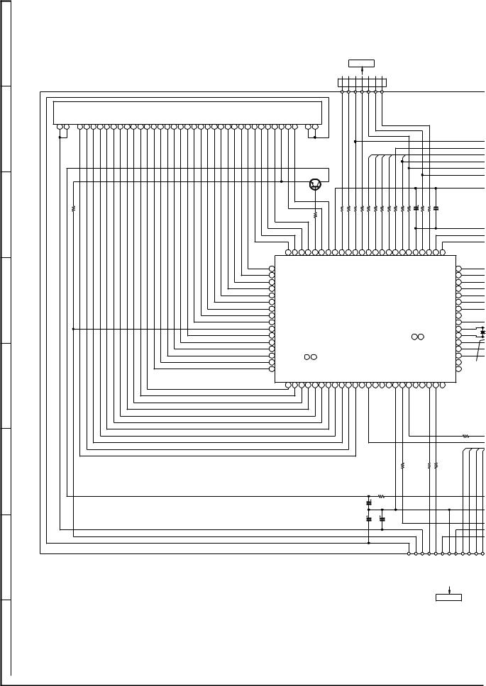
CD-C440W/CP-C440W
A
B
C
D
E
F
G
H
|
|
|
|
|
|
|
|
|
|
|
|
|
|
|
|
|
|
|
|
|
|
|
|
|
|
|
|
|
|
|
|
|
|
|
|
|
|
|
|
|
|
|
|
|
|
WT502 |
|
|
P21 7-A |
|
|
|
|
|
|
|
|
|
||||||
|
|
|
|
|
|
|
|
|
|
|
|
|
|
|
|
|
|
|
|
|
|
|
|
|
|
|
|
|
|
|
|
|
|
|
|
|
|
|
|
|
|
|
|
|
|
TO MAIN PWB |
|
|
|
|
|
|
|
|||||||||||
|
|
|
|
|
|
|
|
|
|
|
|
|
|
|
|
|
|
|
|
|
|
|
|
|
|
|
|
|
|
|
|
|
|
|
|
|
|
|
|
|
|
|
|
|
|
|
|
|
|
|
|
FW702 |
|
|
|
|
|
|
|
|
|
|
||
|
|
|
|
|
|
|
|
|
|
|
|
|
|
|
|
|
|
|
|
|
|
|
|
|
|
|
|
|
|
|
|
|
|
|
|
|
|
|
|
|
|
|
1 |
|
|
|
|
|
|
7 |
|
|
|
|
|
|
|
|
|
|
|
|
||
|
|
|
|
|
FL701 |
|
|
|
|
|
|
|
|
|
|
|
|
|
|
|
|
|
|
|
|
|
|
|
|
|
|
|
|
|
|
|
|
|
|
|
|
CLK |
DO |
DI |
CE |
TUN MUTE |
TUN SD |
TUN SM |
|
|
|
|
|
|
|
|
|
|
|
|
|
|||
F |
F |
S22 |
S21 |
S20 |
S19 |
S18 |
S17 |
S16 |
S15 |
S14 |
S13 |
S12 |
S11 |
S10 |
S09 |
S08 |
S07 |
S06 |
S05 |
S04 |
S03 |
S02 |
S01 |
G11 |
G10 |
G09 |
G08 |
G07 |
G06 |
G05 |
G04 |
G03 |
G02 |
G01 |
|
F |
F |
|
|
|
|
|
|
|
|
|
|
|
|
|
|
|
|
|
||||||||||
41 |
40 |
37 |
36 |
35 |
34 |
33 |
32 |
31 |
30 |
29 |
28 |
27 |
26 |
25 |
24 |
23 |
22 |
21 |
20 |
19 |
18 |
17 |
16 |
15 |
14 |
13 |
12 |
11 |
10 |
9 |
8 |
7 |
6 |
5 |
|
2 |
1 |
|
|
|
|
|
|
|
|
|
|
|
|
|
|
|
|
|
|
|
|
|
|
|
|
|
||
|
|
|
|
|
|
|
|
|
|
|
|
|
|
|
|
|
|
|
|
|
|
|
|
|
|
|
|
|
|
|
|
|
|
|
|
|
|
|
|
|
|
|
|
|
|
|
|
MAIN STB |
MAIN SCK |
MAIN SI |
MAIN SO |
CLEAR |
|
|
|
|
|
|
|
|
|
R |
||
|
|
|
|
|
|
|
|
|
|
|
|
|
|
|
|
|
|
|
|
|
|
|
|
|
|
|
|
|
|
|
|
|
|
|
|
|
|
|
|
|
|
|
|
|
|
|
|
|
|
|
|
|
|
|
|
|
R |
|||||||
|
|
|
|
|
|
|
|
|
|
|
|
|
|
|
|
|
|
|
|
|
|
|
|
|
|
|
|
|
|
|
|
|
|
|
|
|
|
Q701 |
|
|
|
|
|
|
|
|
|
|
|
|
|
|
|
|
R |
|||||||||
|
|
–B |
|
|
|
|
|
|
|
|
|
|
|
|
|
|
|
|
|
|
|
|
|
|
|
|
|
|
|
|
|
|
|
|
|
|
KTC3199 GR |
|
|
|
|
|
|
|
|
|
|
|
|
|
|
|
|
|||||||||||
|
|
|
|
|
|
|
|
|
|
|
|
|
|
|
|
|
|
|
|
|
|
|
|
|
|
|
|
|
|
|
|
|
|
|
|
|
|
|
|
|
|
|
|
|
|
|
|
|
|
|
|
|
|
|
|
|
||||||||
|
|
|
|
|
|
|
|
|
|
|
|
|
|
|
|
|
|
|
|
|
|
|
|
|
|
|
|
|
|
|
|
|
|
|
|
–28.4V |
|
4.8V |
|
+B |
|
|
|
|
|
|
|
|
|
|
|
|
|
|||||||||||
|
|
|
|
|
|
|
|
|
|
|
|
|
|
|
|
|
|
|
|
|
|
|
|
|
|
|
|
|
|
|
|
|
|
|
|
|
|
|
|
|
|
|
|
|
|
|
|
|
|
|
|
|
|
|
|
|
|
|||||||
|
|
|
|
|
|
|
|
|
|
|
|
|
|
|
|
|
|
|
|
|
|
|
|
|
|
|
|
|
|
|
|
|
|
|
|
|
|
|
–28.4V |
|
|
|
|
|
|
|
|
|
|
|
|
|
|
|
.3 |
|
|
|
|
|
|
|
||
|
|
|
|
|
|
|
|
|
|
|
|
|
|
|
|
|
|
|
|
|
|
|
|
|
|
|
|
|
|
|
|
|
|
|
|
|
|
|
|
|
|
|
|
|
|
|
|
|
|
|
|
|
|
C702 20/62 |
|
|
C701 0.022 |
|
|
|
|
|||
|
|
R778 |
100K |
|
|
|
|
|
|
|
|
|
|
|
|
|
|
|
|
|
|
|
|
|
|
|
|
|
|
|
|
|
|
|
|
|
R776 |
|
|
|
R701 1K |
R702 1K |
R703 1K |
R704 1K |
R705 1K |
R706 1K |
R707 1K |
R708 1K |
R709 1K |
R710 1K |
R711 100 |
R712 1K |
R713 1K |
|
|
|
|
|||||||
|
|
|
|
|
|
|
|
|
|
|
|
|
|
|
|
|
|
|
|
|
|
|
|
|
|
|
|
|
|
|
|
|
|
|
|
1K |
|
|
|
|
|
|
|
|||||||||||||||||||||
|
|
|
|
|
|
|
|
|
|
|
|
|
|
|
|
|
|
|
|
|
|
|
|
|
|
|
|
|
|
|
|
|
|
|
|
|
|
|
|
|
|
|
|
|
||||||||||||||||||||
|
|
|
|
|
|
|
|
|
|
|
|
|
|
|
|
|
|
|
|
|
|
|
|
|
|
|
|
|
|
|
|
|
|
|
|
|
|
|
|
|
|
|
|
|
|
|
|
|
|
|
COM DATA RESET |
CLEAR |
TUN MUTE |
TUN SD |
TUN SM |
KEY-5 |
|
|
R |
|||||
|
|
|
|
|
|
|
|
|
|
|
|
|
|
|
|
|
|
|
|
|
|
|
|
|
|
|
|
|
|
|
|
|
|
7G |
6G |
5G |
4G |
3G |
2G |
1G |
|
CLK |
DO |
|
CE |
STB |
CLK |
|
KEY-4 |
|
|
R |
||||||||||||
|
|
|
|
|
|
|
|
|
|
|
|
|
|
|
|
|
|
|
|
|
|
|
|
|
|
|
|
|
|
|
|
|
|
|
DI |
|
|
|
|
|
||||||||||||||||||||||||
|
|
|
|
|
|
|
|
|
|
|
|
|
|
|
|
|
|
|
|
|
|
|
|
|
|
|
|
|
|
|
|
|
|
|
1 |
2 |
3 |
4 |
5 |
6 |
7 |
|
8 |
9 |
10 |
11 |
12 |
13 |
14 |
15 |
16 |
17 |
18 |
19 |
20 |
21 |
22 |
23 |
24 |
|
|
|
||
|
|
|
|
|
|
|
|
|
|
|
|
|
|
|
|
|
|
|
|
|
|
|
|
|
|
|
|
|
|
8G |
|
80 |
P95/ |
P94/FIP6 |
P93/FIP5 |
P92/FIP4 |
P91/FIP3 |
P90/FIP2 |
P81/FIP1 |
P80/FIP0 |
|
VDD |
P27/SCK0 |
P26/SO0/SB1 |
P25/SI0/SB0 |
P24/BUSY |
|
P23/STB |
P22/SCK1 |
P21/SO1 |
P20/SI1 |
RESET |
P74 |
|
P73 |
AVSS |
P17/ANI7 |
P16/ANI6 |
P15/ANI5 |
P13/ |
25 |
KEY-3 |
R |
|
|
|
|
|
|
|
|
|
|
|
|
|
|
|
|
|
|
|
|
|
|
|
|
|
|
|
|
|
|
|
9G |
|
|
FIP7 |
|
|
|
ANI3 |
|
KEY-2 |
R |
||||||||||||||||||||||||
|
|
|
|
|
|
|
|
|
|
|
|
|
|
|
|
|
|
|
|
|
|
|
|
|
|
|
|
|
|
|
|
P96/ |
|
|
|
P12/ |
|
|||||||||||||||||||||||||||
|
|
|
|
|
|
|
|
|
|
|
|
|
|
|
|
|
|
|
|
|
|
|
|
|
|
|
|
|
|
10G |
|
79 |
FIP8 |
|
|
|
P14/ANI4ANI2 |
26 |
KEY-1 |
R |
||||||||||||||||||||||||
|
|
|
|
|
|
|
|
|
|
|
|
|
|
|
|
|
|
|
|
|
|
|
|
|
|
|
|
|
|
|
78 |
P97/ |
|
|
|
|
|
|
|
|
|
|
|
|
|
|
|
|
|
|
|
|
|
|
|
|
|
P11/ANI1 |
27 |
|||||
|
|
|
|
|
|
|
|
|
|
|
|
|
|
|
|
|
|
|
|
|
|
|
|
|
|
|
|
|
|
11G |
|
|
FIP9 |
|
|
|
|
|
|
|
|
|
|
|
|
|
|
|
|
|
|
|
|
|
|
|
|
|
|
|
|
KEY-0 |
R |
|
|
|
|
|
|
|
|
|
|
|
|
|
|
|
|
|
|
|
|
|
|
|
|
|
|
|
|
|
|
|
|
77 |
|
P100/ |
|
|
|
|
|
|
|
|
|
|
|
|
|
|
|
|
|
|
|
|
|
|
|
|
|
P10/ANI0 |
28 |
||||
|
|
|
|
|
|
|
|
|
|
|
|
|
|
|
|
|
|
|
|
|
|
|
|
|
|
|
|
|
|
P1 |
|
|
|
FIP10 |
|
|
|
|
|
|
|
|
|
|
|
|
|
|
|
|
|
|
|
|
|
|
|
|
|
|
|
|
AVDD |
|
|
|
|
|
|
|
|
|
|
|
|
|
|
|
|
|
|
|
|
|
|
|
|
|
|
|
|
|
|
|
|
76 |
|
P101/ |
|
|
|
|
|
|
|
|
|
|
|
|
|
|
|
|
|
|
|
|
|
|
|
|
|
|
AVDD |
29 |
|
||
|
|
|
|
|
|
|
|
|
|
|
|
|
|
|
|
|
|
|
|
|
|
|
|
|
|
|
|
|
|
P2 |
|
|
|
FIP11 |
|
|
|
|
|
|
|
|
|
|
|
|
|
|
|
|
|
|
|
|
|
|
|
|
|
|
|
|
AVREF |
|
|
|
|
|
|
|
|
|
|
|
|
|
|
|
|
|
|
|
|
|
|
|
|
|
|
|
|
|
|
|
|
75 |
|
P102/ |
|
|
|
|
|
|
|
|
|
|
|
|
|
|
|
|
|
|
|
|
|
|
|
|
|
|
AVREF |
30 |
|||
|
|
|
|
|
|
|
|
|
|
|
|
|
|
|
|
|
|
|
|
|
|
|
|
|
|
|
|
|
|
P3 |
|
|
|
FIP12 |
|
|
|
|
|
|
|
|
|
|
IC701 |
|
|
|
|
|
|
|
|
|
|
|
|
|
|
P04 |
|
|||
|
|
|
|
|
|
|
|
|
|
|
|
|
|
|
|
|
|
|
|
|
|
|
|
|
|
|
|
|
|
|
74 |
|
P103/ |
|
|
|
|
|
|
|
|
|
|
|
|
|
|
|
|
|
|
|
|
|
|
P04/XT1 |
31 |
|
||||||
|
|
|
|
|
|
|
|
|
|
|
|
|
|
|
|
|
|
|
|
|
|
|
|
|
|
|
|
|
|
P4 |
|
|
FIP13 |
|
|
|
|
|
|
|
|
|
|
|
|
|
|
|
|
|
|
|
|
|
|
|
|
|||||||
|
|
|
|
|
|
|
|
|
|
|
|
|
|
|
|
|
|
|
|
|
|
|
|
|
|
|
|
|
|
|
73 |
|
P104/ |
|
|
|
|
|
|
|
|
IX0170AW |
|
|
|
|
|
|
|
|
|
|
XT2 |
32 |
XT2 |
|
||||||||
|
|
|
|
|
|
|
|
|
|
|
|
|
|
|
|
|
|
|
|
|
|
|
|
|
|
|
|
|
|
P5 |
|
|
|
FIP14 |
|
|
|
|
|
|
|
|
|
|
|
|
|
|
P31/TO1 |
P32/TO2 |
|
|
|
|
VSS |
|
||||||||
|
|
–B |
|
|
|
|
|
|
|
|
|
|
|
|
|
|
|
|
|
|
|
|
|
|
|
|
|
|
|
|
72 |
|
P105/ |
|
|
|
SYSTEM MICROCOMPUTER |
|
|
|
VSS |
33 |
|
|||||||||||||||||||||
|
|
|
|
|
|
|
|
|
|
|
|
|
|
|
|
|
|
|
|
|
|
|
|
–B |
|
|
|
VLOAD |
|
|
FIP15 |
|
|
|
|
|
|
X1 |
|
|||||||||||||||||||||||||
|
|
|
|
|
|
|
|
|
|
|
|
|
|
|
|
|
|
|
|
|
|
|
|
|
|
|
|
71 |
|
VLOAD |
|
|
|
|
|
|
|
|
|
|
|
|
|
|
|
|
|
|
|
|
|
|
|
|
34 |
|
||||||||
|
|
|
|
|
|
|
|
|
|
|
|
|
|
|
|
|
|
|
|
|
|
|
|
|
|
|
|
|
P6 |
|
|
|
P106/ |
|
|
|
|
|
|
|
|
|
|
|
|
|
|
|
|
|
|
|
|
|
|
|
|
|
|
X2 |
|
|||
|
|
|
|
|
|
|
|
|
|
|
|
|
|
|
|
|
|
|
|
|
|
|
|
|
|
|
|
|
|
|
70 |
|
|
|
|
|
|
|
|
|
|
|
|
|
|
|
|
|
|
|
|
|
|
|
42 |
41 |
|
|
|
35 |
|
|||
|
|
|
|
|
|
|
|
|
|
|
|
|
|
|
|
|
|
|
|
|
|
|
|
|
|
|
|
|
|
P7 |
|
|
|
FIP16 |
|
|
|
|
|
|
|
|
|
|
|
|
|
|
|
|
|
|
|
|
|
|
|
|
|
|
CE |
|
||
|
|
|
|
|
|
|
|
|
|
|
|
|
|
|
|
|
|
|
|
|
|
|
|
|
|
|
|
|
|
|
69 |
|
P107/ |
|
|
P114/ FIP22 |
P115/ FIP23 |
|
|
|
|
|
|
|
|
|
|
|
|
|
|
|
|
|
|
|
|
|
P37 |
36 |
R |
|||
|
|
|
|
|
|
|
|
|
|
|
|
|
|
|
|
|
|
|
|
|
|
|
|
|
|
|
|
|
|
P8 |
|
|
|
FIP17 |
|
|
|
|
|
|
|
|
|
|
|
|
|
|
|
|
|
|
|
|
|
|
|
|
|
DI |
||||
|
|
|
|
|
|
|
|
|
|
|
|
|
|
|
|
|
|
|
|
|
|
|
|
|
|
|
|
|
|
|
68 |
|
P110/ |
|
|
|
|
|
|
|
|
|
|
|
|
|
|
|
|
|
|
|
|
|
|
P36/BUZ |
37 |
R |
||||||
|
|
|
|
|
|
|
|
|
|
|
|
|
|
|
|
|
|
|
|
|
|
|
|
|
|
|
|
|
|
P9 |
|
|
FIP18 |
|
|
|
|
|
|
|
|
|
|
|
|
|
|
|
|
|
|
|
|
|
|
CL |
||||||||
|
|
|
|
|
|
|
|
|
|
|
|
|
|
|
|
|
|
|
|
|
|
|
|
|
|
|
|
|
|
|
67 |
|
P111/ |
|
|
|
64 |
63 |
|
|
|
|
|
|
|
|
|
|
|
|
|
|
P00/INTP0/TI0 |
|
|
|
P03/INTP3/CI0 |
|
|
P35/PCL |
38 |
R |
||
|
|
|
|
|
|
|
|
|
|
|
|
|
|
|
|
|
|
|
|
|
|
|
|
|
|
|
|
|
|
P10 |
|
|
|
FIP19 |
|
|
|
|
|
|
|
|
|
|
|
|
|
|
|
|
|
|
|
|
|
|
|
|
|
|||||
|
|
|
|
|
|
|
|
|
|
|
|
|
|
|
|
|
|
|
|
|
|
|
|
|
|
|
|
|
|
|
66 |
|
P112/ |
|
|
|
|
|
|
|
|
|
|
|
|
|
|
|
|
|
|
|
|
P01/INTP1 |
P02/INTP2 |
|
|
P34/TI2 |
39 |
C704 |
||||
|
|
|
|
|
|
|
|
|
|
|
|
|
|
|
|
|
|
|
|
|
|
|
|
|
|
|
|
|
|
P11 |
|
|
FIP20 |
|
|
|
|
|
|
|
|
|
|
|
|
|
|
|
|
|
|
|
|
P30/TO0 |
|
|||||||||
|
|
|
|
|
|
|
|
|
|
|
|
|
|
|
|
|
|
|
|
|
|
|
|
|
|
|
|
|
|
|
65 |
|
P113/ |
|
|
|
|
|
|
|
|
|
|
|
|
|
|
|
|
|
|
|
|
|
P33/ |
40 |
18P |
|||||||
|
|
|
|
|
|
|
|
|
|
|
|
|
|
|
|
|
|
|
|
|
|
|
|
|
|
|
|
|
|
|
|
|
|
FIP21 |
|
|
P116/ FIP24 |
P117/ FIP25 |
P120/ FIP26 |
P121/ FIP27 |
P122/ FIP28 |
P123/ FIP29 |
P124/ FIP30 |
P125/ FIP31 |
P126/ FIP32 P127/ FIP33 |
VDD |
P70 |
P71 |
P72 |
|
|
|
TI1 |
|
(CH) |
|||||||||
|
|
|
|
|
|
|
|
|
|
|
|
|
|
|
|
|
|
|
|
|
|
|
|
|
|
|
|
|
|
|
|
|
|
|
|
|
IC |
|
|
|
|
|
|
|||||||||||||||||||||
|
|
|
|
|
|
|
|
|
|
|
|
|
|
|
|
|
|
|
|
|
|
|
|
|
|
|
|
|
|
|
P12 |
64 |
63 |
62 |
61 |
60 |
59 |
58 |
57 |
56 |
55 |
54 |
53 |
52 |
51 |
50 |
49 |
48 |
47 |
46 |
45 |
44 |
43 |
42 |
41 |
|
|
|
||||||
|
|
|
|
|
|
|
|
|
|
|
|
|
|
|
|
|
|
|
|
|
|
|
|
|
|
|
|
|
|
|
P13 |
|
P14 P15 P16 P17 P18 |
P19 P20 |
P21 |
P22 |
|
VDD |
|
|
VSS |
REMOCON |
SYS STOP |
|
|
POWER |
F MUTE |
|
|
|
|
|||||||||||||
|
|
|
|
|
|
|
|
|
|
|
|
|
|
|
|
|
|
|
|
|
|
|
|
|
|
|
|
|
|
|
|
|
|
|
|
|
|
|
|
|
|
|
|
|
||||||||||||||||||||
|
|
|
|
|
|
|
|
|
|
|
|
|
|
|
|
|
|
|
|
|
|
|
|
|
|
|
|
|
|
|
|
|
|
|
|
|
|
|
|
|
|
|
|
|
|
|
|
|
|
|
|
|
|
|
|
|
|
|
|
|
|
R728 |
|
|
|
|
|
|
|
|
|
|
|
|
|
|
|
|
|
|
|
|
|
|
|
|
|
|
|
|
|
|
|
|
|
|
|
|
|
|
|
|
|
|
|
|
|
|
|
|
|
|
|
|
|
|
|
|
|
|
|
|
|
|
|
|
10K |
|
|
|
|
|
|
|
|
|
|
|
|
|
|
|
|
|
|
|
|
|
|
|
|
|
|
|
|
|
|
|
|
|
|
|
|
|
|
|
|
|
|
|
|
|
|
|
|
|
|
|
|
+B |
|
|
|
|
|
|
|
|
|
|
|
|
|
|
|
|
|
|
|
|
|
|
|
|
|
|
|
|
|
|
|
|
|
|
|
|
|
|
|
|
|
|
|
|
|
|
|
|
|
|
|
|
|
|
|
|
|
|
|
|
|
|
|
|
|
|
|
|
R729 1K |
|
|
|
|
R727 1K |
R726 1K |
|
CLEAR |
MAIN SO MAIN SI |
MAIN SCK |
|
|
|
|
|
|
|
|
|
|
|
|
|
|
|
|
|
|
|
|
|
|
|
|
|
|
|
|
|
|
|
|
|
|
|
|
|
|
|
|
|
|
|
|
|
|
C716 |
|
R777 |
|
|
|
|
|
|
|
|
|
|
|
|
||||
|
|
|
|
|
|
|
|
|
|
|
|
|
|
|
|
|
|
|
|
|
|
|
|
|
|
|
|
|
|
|
|
|
|
|
|
|
|
|
|
|
|
|
|
|
|
47/16 |
|
|
33 |
|
|
|
|
|
|
|
|
|
|
|
|
|
||
|
|
|
|
|
|
|
|
|
|
|
|
|
|
|
|
|
|
|
|
|
|
|
|
|
|
|
|
|
|
|
|
|
|
|
|
|
|
|
|
|
|
|
|
|
|
C712 |
|
|
|
C713 |
|
|
|
|
|
|
|
|
|
|
|
|||
|
|
|
|
|
|
|
|
|
|
|
|
|
|
|
|
|
|
|
|
|
|
|
|
|
|
|
|
|
|
|
|
|
|
|
|
|
|
|
|
|
|
|
|
|
|
1/50 |
|
|
|
1/50 |
|
|
|
|
|
|
|
|
|
|
|
|||
|
|
|
|
|
|
|
|
|
|
|
|
|
|
|
|
|
|
|
|
|
|
|
|
|
|
|
|
|
|
|
|
|
|
|
|
|
|
|
|
|
|
|
|
|
|
|
|
|
|
|
|
|
|
|
|
|
|
|
|
|
+B |
|
|
|
|
|
–B |
|
|
|
|
|
|
|
|
|
|
|
|
|
|
|
|
|
|
|
|
|
|
|
|
|
|
|
|
|
|
|
|
|
|
|
|
|
|
|
|
|
|
|
|
|
|
|
|
|
|
|
|
–B |
|
|
|
+B |
|
|
|
||
DISPLAY PWB-C1 |
13 |
|
|
|
|
|
|
|
|
|
|
|
|
|
VF1 |
–VP |
VF2 |
POWER |
F MUTE |
M 12V |
D GND |
D 5V |
CLEAR |
DO |
DI |
CL |
|
|
|
|
|
|
|
|
|
|
|
|
|
|
|
|
|
|
|
|
|
|
|
|
|
|
|
WT601 TO MAI
P21 7
• NOTES ON SCHEMATIC DIAGRAM can be found on page 12.
1 |
2 |
3 |
4 |
5 |
6 |
Figure 18 SCHEMATIC DIAGRAM (3/14)
– 18 –
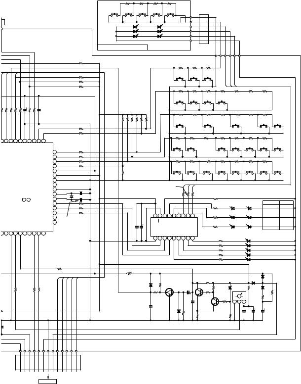
CD-C440W/CP-C440W
P21 7-A
O MAIN PWB
FW702
7
_
|
RD07 |
RD06 |
RD05 |
RD04 |
|
SW708 |
12K |
5.6K |
3.9K |
2.2K |
|
SW707 |
SW706 |
SW705 |
SW704 |
1 |
|
|
|
|
|
|
|
OPEN |
DISK |
DISK 3 |
DISK 2 |
DISK 1 |
|
/CLOSE |
SKIP |
|
|||
|
|
|
|
||
DISC 3 |
LED715 |
LED714 |
|
|
|
DISC 2 |
LED717 |
LED716 |
|
|
|
DISC 1 |
LED719 |
LED718 |
|
|
|
|
|
|
|
+B |
|
DISPLAY PWB-C2 |
LED714~LED719: |
6 |
|||
|
LMKD515B |
FW701 |
|||
|
|
||||
|
|
|
|
|
|
|
|
|
|
|
|
|
|
|
|
R749 |
|
|
|
|
|
|
|
|
|
|
|
|
|
|
|
|
|
|
|
|
1 |
|
|
|
|
6 |
|
|
|
|
|
|
||
|
|
|
|
|
|
|
|
|
|
|
|
|
|
|
|
10K |
+B |
|
|
|
|
|
|
|
|
|
|
|
|
|
|
|
|
|
|
|
|
|
|
|
|
|
|
|
|
|
||||
|
|
|
|
|
|
|
|
|
|
|
|
|
|
|
|
|
|
|
|
|
|
|
|
|
|
|
|
|
|
|
|
|
|
|
|
|
|
|
|
|
|
|
|
|
|
|
|
|
|
|
|
|
|
|
|
|
|
|
|
|
|
|
|
|
|
|
|
|
|
|
|
|
|
|
|
|
|
|
RD01 |
|
RD02 |
|
RD03 |
|
|
|
|
|
|
|
|
|
|
|
|
||||||
|
|
|
|
|
|
|
|
|
|
|
|
|
|
|
R779 |
10K |
|
|
|
|
|
|
|
|
|
|
1K |
|
|
1.2K |
|
|
1.8K |
|
|
|
|
|
|
|
|
|
|
|
+B |
|||||
|
MAIN SO |
CLEAR |
|
|
|
|
|
|
|
|
|
|
|
|
|
|
|
|
|
|
|
|
SW701 |
SW702 |
|
SW703 |
|
|
|
|
|
|
|
|
|
|
|
|||||||||||||
_ |
|
|
|
|
|
|
|
|
|
|
|
R780 |
1.8K |
|
|
|
|
|
|
|
|
|
ON/ |
|
|
CLOCK |
|
TIMER |
|
|
Q7 Q6 |
Q5 |
|
|
|
|
|
|
|
|
||||||||||
|
|
|
|
|
|
|
|
|
|
|
R781 |
10K |
|
|
|
|
|
|
|
|
|
|
|
|
|
|
|
|
|
|
|
|
|
|
||||||||||||||||
|
|
|
|
|
|
|
|
|
|
|
|
|
|
|
|
|
|
|
STAND-BY |
|
|
|
|
|
/SLEEP |
|
|
|
|
|
|
|
|
|
|
|||||||||||||||
|
|
|
|
|
|
|
|
|
|
|
|
|
|
|
|
|
|
|
|
|
|
|
|
|
|
|
|
|
|
|
|
|
|
|
|
|
|
|
|
|
|
|
|
|
||||||
|
|
|
|
|
|
|
|
|
|
|
|
|
|
|
|
|
+B |
|
|
|
|
|
|
|
|
|
RD08 |
|
RD09 |
|
RD10 |
RD11 |
RD12 |
|
RD13 |
|
RD14 |
|
|
|||||||||||
|
|
|
|
|
|
.3 |
|
|
|
|
|
|
|
|
|
|
|
|
|
|
|
|
|
|
|
|
|
1K |
|
|
1.2K |
|
|
1.8K |
|
2.2K |
3.9K |
|
5.6K |
|
|
12K |
|
|
||||||
|
|
|
|
|
|
|
|
|
|
|
|
|
|
|
|
|
|
|
|
|
|
|
|
|
|
SW709 |
SW710 |
|
SW711 |
SW712 |
|
|
|
|
|
|
|
|
|
|||||||||||
|
|
|
|
|
|
C702 220/6 |
|
|
C701 0.022 |
|
|
|
|
|
|
|
|
|
|
|
|
|
|
|
|
|
|
|
|
|
|
|
|
|
|
|
||||||||||||||
DATA R708 1K RESET R709 1K CLEAR R710 1K |
TUN MUTE R711 100 |
1K |
1K |
|
|
|
|
|
|
|
|
|
R736 8.2K |
R735 8.2K R734 8.2K R733 8.2K R732 8.2K R731 |
|
|
|
|
|
|
CD |
|
|
TUNER |
|
|
TAPE |
VIDEO |
|
|
|
|
|
|
|
|
|
|||||||||||||
|
|
|
|
|
|
|
|
|
|
|
|
|
|
|
|
|
|
|
|
/BAND |
|
|
|
|
|
|
|
|
|
|
|
|||||||||||||||||||
R712 |
R713 |
|
|
|
|
|
|
|
|
+B |
|
|
|
|
|
|
|
|
|
|
|
|
|
|
|
|
|
|
|
|
|
|
|
|
|
|
|
|
|
|||||||||||
|
|
|
|
|
|
|
|
|
8.2K |
|
|
|
|
|
RD15 |
|
RD16 |
|
RD17 |
RD18 |
RD19 |
|
RD20 |
|
RD21 |
|
|
|||||||||||||||||||||||
|
|
|
|
|
|
|
|
|
|
|
|
|
|
1K |
|
|
1.2K |
|
|
1.8K |
|
2.2K |
3.9K |
|
5.6K |
|
|
12K |
SW724 |
|||||||||||||||||||||
|
|
|
|
|
|
|
|
|
|
|
|
|
|
|
|
|
|
|
|
|
|
|
|
|||||||||||||||||||||||||||
TUN SD |
TUN SM |
|
|
|
|
|
|
|
|
|
|
|
|
|
SW717 |
|
|
|
|
|
SW719 |
|
|
|
SW721 |
|
|
|
SW723 |
|||||||||||||||||||||
KEY-5 |
|
|
|
R714 |
1K |
|
|
|
|
|
|
|
|
CENTER |
|
|
|
|
|
CENTER |
|
|
DOLBY |
|
REC/ |
TUNING |
||||||||||||||||||||||||
|
KEY-4 |
|
|
|
R715 |
1K |
|
|
|
|
|
|
|
|
MODE/ |
|
|
|
|
|
MODE/ |
|
|
LOGIC/ |
|
|||||||||||||||||||||||||
|
|
|
|
|
|
|
|
|
|
|
|
PHANTOM |
|
|
|
|
NORMAL |
|
|
BYPASS |
|
PAUSE |
UP/TIME |
|||||||||||||||||||||||||||
|
|
|
|
|
|
|
|
|
|
|
|
|
RD22 |
|
RD23 |
|
|
|
|
|
RD25 |
RD26 |
|
RD27 |
|
RD28 |
|
|
||||||||||||||||||||||
5 |
16 |
17 |
18 |
19 |
20 |
21 |
22 |
23 |
24 |
|
|
|
|
|
|
|
|
|
|
|
|
|
|
|
|
|
RD24 |
|
|
|
|
|||||||||||||||||||
P21/SO1 |
P20/SI1 |
RESET |
P74 |
|
P73 |
AVSS |
P17/ANI7 |
P16/ANI6 |
P15/ANI5 |
|
|
|
|
|
|
|
|
|
|
|
|
|
|
|
|
1K |
|
|
1.2K |
|
1.8K |
|
2.2K |
3.9K |
|
5.6K |
|
|
12K |
SW732 |
||||||||||
|
|
|
|
|
|
|
|
|
|
|
|
|
|
|
|
SW725 |
SW726 |
|
|
|
|
|
SW728 |
SW729 |
SW730 |
|
SW731 |
|||||||||||||||||||||||
|
P13/ |
|
KEY-3 |
R716 |
1K |
|
|
|
|
|
|
|
|
|
|
|
|
|
|
|
|
|
|
|
|
|
|
|
|
|
|
|
|
|
|
|
|
|
||||||||||||
|
P14/ANI4ANI3 |
25 |
|
|
R717 |
1K |
|
|
|
|
|
|
|
|
VOLUME |
|
X-BASS |
|
|
|
|
|
STOP |
FWD |
|
FF |
MEMORY |
TUNING |
||||||||||||||||||||||
|
|
|
|
|
|
|
|
|
|
|
P12/ |
26 KEY-2 |
|
|
|
|
|
|
|
|
|
UP |
|
|
|
|
|
|
|
|
|
|
|
|
|
|
|
|
|
|
/SET |
DOWN |
|
|||||||
|
|
|
|
|
|
|
|
|
|
|
ANI2 |
|
KEY-1 |
R718 |
1K |
|
|
|
|
|
|
|
|
|
|
|
|
|
|
|
|
|
|
|
|
|
|
|
|
|
|
|
|
|
|
|
|
|
||
|
|
|
|
|
|
|
|
|
|
P11/ANI1 |
27 |
|
|
|
|
|
|
|
|
RD29 |
|
RD30 |
|
|
RD31 |
RD32 |
RD33 |
|
RD34 |
|
RD35 |
|
|
|||||||||||||||||
|
|
|
|
|
|
|
|
|
|
P10/ANI0 |
28 |
KEY-0 |
R719 |
1K |
|
|
|
|
|
|
|
|
|
|
|
|
|
|
|
|||||||||||||||||||||
|
|
|
|
|
|
|
|
|
|
|
|
|
|
|
|
|
|
|
|
|
|
|
|
1K |
|
|
1.2K |
|
|
1.8K |
|
2.2K |
3.9K |
|
5.6K |
|
|
12K |
|
|
||||||||||
|
|
|
|
|
|
|
|
|
|
|
AVDD |
29 AVDD |
|
|
|
+B |
|
RD36 |
|
|
|
|
|
SW733 |
SW734 |
|
SW735 |
SW736 |
SW737 |
SW738 |
|
SW739 |
SW740 |
|||||||||||||||||
|
|
|
|
|
|
|
|
|
|
|
AVREF |
30 AVREF |
|
|
|
|
15K |
|
|
|
|
VOLUME |
|
|
EQ. |
|
|
|
3D |
|
REVERSE |
REV |
|
REW |
|
EDIT |
EDIT |
|
||||||||||||
|
|
|
|
|
|
|
|
|
|
|
P04/XT1 |
31 P04 |
|
|
|
|
|
|
|
|
|
|
|
DOWN |
|
/DEMO |
SURROUND |
|
NORMAL |
HIGH |
|
|||||||||||||||||||
|
|
|
|
|
|
|
|
|
|
|
|
|
|
|
|
|
|
|
|
|
|
|
|
|
|
|
|
|
|
|
||||||||||||||||||||
|
|
|
|
|
|
|
|
|
|
|
|
|
|
|
|
|
|
|
|
|
|
|
|
|
|
|
|
|
|
|
|
|
|
|
|
|||||||||||||||
|
|
|
|
|
|
|
|
|
|
|
XT2 |
32 |
XT2 |
|
|
C703 |
|
|
|
|
|
|
|
R747 |
|
|
|
|
|
|
|
|
|
|
|
|
|
|
|
|
|
|
|
|
|
|
|
|||
PUTER |
|
P31/TO1 |
P32/TO2 |
|
|
|
VSS |
33 |
VSS |
|
|
|
|
|
|
|
|
|
|
820 |
Q7 |
Q6 |
Q5 |
|
|
|
|
|
|
|
|
|
|
|
|
|
|
|
|
|
|
|||||||||
|
|
|
|
X1 |
|
|
|
15P |
|
|
|
|
|
|
|
|
|
|
|
|
|
|
|
|
|
|
|
|
|
|
|
|
|
|
|
|
||||||||||||||
|
|
|
|
|
|
|
|
|
|
|
|
|
|
|
|
|
|
R746 |
|
|
R745 |
|
|
|
|
|
|
|
|
|
|
|
||||||||||||||||||
|
|
|
|
|
|
|
|
|
|
34 |
|
|
|
(CH) |
+B |
|
|
|
|
|
|
|
|
R748 |
|
|
|
|
|
|
|
|
|
|
|
|
|
|
||||||||||||
|
|
|
|
|
|
|
|
|
|
|
|
|
|
|
|
|
|
|
|
|
|
|
|
820 |
|
820 |
|
|
1K |
|
|
|
|
|
|
|
|
|
|
|
||||||||||
|
|
|
|
|
|
42 |
41 |
|
|
|
|
35 |
X2 |
|
|
XL701 |
|
|
|
|
+B |
|
|
|
|
|
|
|
|
|
|
|
|
|
|
|
|
|
|
LED710 |
|
LED711 |
|
|
SRS ON |
|||||
|
|
|
|
|
|
|
|
|
|
|
CE |
|
|
|
|
|
|
|
|
|
|
|
|
|
|
|
|
|
|
|
|
|
|
|
|
R744 |
|
|
DOLBY |
SRS |
||||||||||
|
|
|
|
|
|
|
|
|
|
|
|
|
|
|
|
|
|
|
|
|
|
|
|
|
|
|
|
|
|
|
|
|
|
|
|
|
|
|
||||||||||||
|
|
|
|
|
|
|
|
|
|
|
P37 |
36 |
|
|
|
R720 |
1K |
|
|
|
|
|
|
|
|
|
|
|
|
|
|
|
|
|
|
|
|
5N4YTN52 5N4YTN52 |
|
|||||||||||
|
|
|
|
|
|
|
|
|
|
P36/BUZ |
37 |
DI |
|
|
|
|
|
|
|
|
|
|
|
|
|
|
|
|
|
|
|
|
|
|
820 |
|
|
|
|
|
|
|
|
PHANTOM STEREO |
||||||
|
|
|
|
|
|
|
|
|
|
|
|
R721 |
1K |
|
|
|
|
|
|
|
|
|
|
|
|
|
|
|
|
|
|
|
|
|
|
|
|
|
|
|
|
|
|
|||||||
|
|
|
|
|
|
|
P03/INTP3/CI0 |
|
|
|
P35/PCL |
38 |
CL |
|
|
|
|
|
|
|
|
|
|
|
|
|
|
|
|
|
|
|
|
|
|
R743 |
|
LED708 |
|
LED709 |
|
|
|
|
||||||
|
|
|
P00/INTP0/TI0 |
|
|
|
|
|
|
|
|
R722 |
1K |
|
|
|
|
|
|
|
|
|
|
|
|
|
|
|
|
|
|
|
|
|
|
|
NORMAL |
MONO |
||||||||||||
|
|
|
|
P01/INTP1 |
P02/INTP2 |
|
|
|
P34/TI2 |
39 |
|
C704 |
|
|
C730 0.022 |
C729 47/16 |
18 |
17 |
16 |
15 14 |
13 |
12 |
11 |
10 |
|
|
|
|
|
820 |
|
5N4YTN52 5N4YTN52 |
|
|||||||||||||||||
|
|
|
|
P30/TO0 |
|
|
|
|
|
|
|
VDD |
OE |
Q11 |
Q10 |
Q9 |
Q8 |
Q7 |
Q6 |
Q5 |
|
|
|
|
|
R742 |
|
LED706 |
|
LED707 |
|
|
|
|
||||||||||||||||
|
|
|
|
|
|
P33/ |
40 |
|
18P |
|
|
|
|
|
|
|
|
|
|
|
|
|
|
|
||||||||||||||||||||||||||
P71 |
P72 |
IC |
|
|
|
TI1 |
|
|
(CH) |
|
|
|
|
|
|
|
|
|
820 |
|
5N4YTN52 5N4YTN52 |
|
PASS |
PASS |
||||||||||||||||||||||||||
|
|
|
|
|
|
|
|
|
|
|
|
|
|
|
|
|
|
|
|
|
|
|
|
|
|
|
|
|
|
|||||||||||||||||||||
0 |
49 |
48 |
47 |
46 |
45 |
44 |
43 |
42 |
41 |
|
|
|
|
|
|
|
|
|
|
VSS |
DATA |
CLOCK |
LCK |
Q0 |
Q1 |
Q2 |
Q3 |
Q4 |
|
|
IC702 |
|
|
INPUT/OUTPUT |
|
|
|
|
||||||||||||
|
VSS REMOCON |
SYS STOP |
|
|
POWER |
F MUTE |
|
|
|
|
|
|
|
|
|
|
|
|
1 |
2 |
3 |
4 |
5 |
6 |
7 |
8 |
9 |
|
|
BU2092F EXPANDER |
|
|
|
|
|
|||||||||||||||
|
|
|
|
|
|
|
|
|
|
|
|
|
|
|
|
|
|
|
|
R741 |
|
1K |
LED705 |
5N4GTN52 REV |
|
|||||||||||||||||||||||||
|
|
|
|
|
|
|
|
|
|
|
|
|
|
|
|
|
|
|
|
|
|
|
|
|
|
|
|
|
|
|
R740 |
|
1K |
LED704 |
5N4GTN52 REW |
|
||||||||||||||
|
|
|
|
|
|
|
|
|
|
|
|
|
|
|
|
|
|
|
|
|
|
|
|
|
|
|
|
|
|
|
R739 |
|
1K |
LED703 |
5N4GTN52 STOP |
|
||||||||||||||
|
|
|
|
|
|
|
|
|
|
|
|
|
|
|
|
|
|
|
|
|
|
|
|
|
|
|
|
|
|
|
R738 |
|
1K |
LED702 |
5N4GTN52 FF |
|
||||||||||||||
|
|
|
|
|
|
|
|
|
|
|
|
|
|
|
|
|
|
+B |
|
|
|
|
|
|
|
|
|
|
|
|
|
|
|
|
|
|
|
R737 |
|
1K |
LED701 |
5N4GTN52 PLAY |
|
|||||||
|
|
|
|
|
|
|
|
|
|
|
|
R728 |
|
|
|
|
|
|
|
|
|
|
|
|
|
|
|
|
|
|
|
|
|
|
|
|
|
|
|
|
+B |
|
|
|
|
|
||||
|
|
|
|
|
|
|
|
|
|
|
|
|
|
|
|
|
|
|
|
|
|
|
|
|
|
|
|
|
|
|
|
|
|
|
|
|
|
|
|
|
|
|
|
|
|
|||||
|
|
|
|
|
|
|
|
|
|
|
|
10K |
|
|
|
|
|
|
|
|
|
|
|
|
|
|
|
|
|
|
|
|
|
|
|
|
|
|
|
|
|
|
|
|
|
D708 |
|
|
||
|
|
|
|
|
|
|
|
|
|
|
|
|
|
|
|
|
|
|
|
|
|
|
|
|
|
|
|
|
|
|
|
|
|
|
|
|
|
|
|
|
|
|
|
|
|
|
|
|
||
|
|
|
|
|
|
|
|
|
|
|
|
|
|
|
|
|
+B |
|
|
|
5V BACK UP |
|
|
|
+B |
|
|
|
|
|
|
|
|
|
|
|
|
|
|
|
|
1SS133 |
|
|
||||||
|
|
|
|
|
|
|
|
|
|
|
|
|
|
|
|
|
|
|
|
L701 |
|
|
|
|
|
|
|
|
|
|
|
|
Q705 |
|
|
|
|
ZD701 |
|
|
D707 |
|
|
|
||||||
|
|
|
|
|
|
|
|
|
|
|
|
|
|
|
|
|
|
|
|
|
|
|
|
|
|
|
|
|
|
|
|
|
KTC3199 GR |
|
|
|
1SS133 |
|
|
|
||||||||||
|
|
|
|
|
|
|
|
|
|
|
|
CLEAR |
MAIN SO |
MAIN SI |
MAIN SCK |
MAIN STB |
|
|
|
100 H |
D705 |
R765 3.3K |
|
|
Q704 |
|
|
|
|
|
|
|
|
|
|
|
+B MTZJ3.9B |
|
|
+B |
|
|||||||||
|
|
|
R729 1K |
|
|
|
|
R727 1K |
R726 1K |
|
|
|
|
|
|
|
|
|
|
|
|
|
|
|
|
|
|
|
|
|
|
|
D709 1SS133 |
|
||||||||||||||||
|
|
|
|
|
|
|
|
|
|
|
|
|
|
|
|
|
|
|
|
4.8V |
|
|
R770 |
|
|
|
|
|
|
|
|
|
|
|
||||||||||||||||
|
|
|
|
|
|
|
|
|
|
|
|
|
1SS133 |
|
KRC102 M |
C707 |
|
|
|
R769 |
|
|
|
R773 |
|
|
|
|||||||||||||||||||||||
|
|
|
|
|
|
|
|
|
|
|
|
|
|
|
|
|
|
|
|
3.3/50 |
|
|
0V |
1K |
10K |
RX701 |
27 |
|
|
R775 2.2K |
|
|||||||||||||||||||
|
|
|
|
|
|
|
|
|
|
|
|
|
|
|
|
2 |
|
|
3 |
|
|
|
|
|
|
|
R768 |
0V |
|
R771 |
|
|
|
R774 |
|
|||||||||||||||
|
|
|
|
|
|
|
|
|
|
|
|
|
|
R763 5V |
|
0V |
|
|
|
|
|
|
|
|
|
|
|
|||||||||||||||||||||||
|
|
|
|
|
|
|
|
|
|
|
|
|
|
1K |
|
|
1 |
0V |
|
|
C708 |
0.01 |
|
0V |
10K |
|
|
100 |
1 |
2 |
3 |
|
150 |
|
||||||||||||||||
|
|
|
|
|
|
|
|
|
|
|
|
|
|
|
|
|
|
|
|
|
|
|
|
|
|
|
|
|
|
|
|
|||||||||||||||||||
|
|
|
|
|
|
|
|
|
|
|
|
|
C706 |
|
|
|
|
|
|
|
|
|
|
|
|
|
|
|
0V |
|
|
|
|
|||||||||||||||||
|
|
|
|
|
|
|
|
|
|
|
|
|
|
|
|
|
|
1SS133 |
|
|
|
|
|
|
|
|
|
|
|
|
|
220/6.3 |
|
|||||||||||||||||
|
|
|
|
|
|
|
|
|
|
|
|
|
|
|
|
|
|
|
|
|
0.01 |
|
|
|
|
D706 |
|
R766 100K |
|
|
|
|
|
|
0V |
Q706 |
|
|
|
C715 0.022 |
C710 |
C709 |
|
|||||||
|
|
|
|
|
|
|
|
|
|
|
|
|
|
|
|
|
|
|
|
|
|
|
|
|
|
|
|
|
|
|
|
|
|
|
|
|
100/6.3 |
|
||||||||||||
77 |
|
|
|
|
|
|
|
|
|
|
|
|
|
|
|
|
|
|
|
|
|
|
|
|
|
|
|
R767 |
KTC3199 GR |
|
|
|
|
|||||||||||||||||
|
|
|
|
|
|
|
|
|
|
|
|
|
|
|
|
|
|
|
|
|
|
|
|
|
|
|
|
|
|
R772 |
|
|
|
|
|
|
||||||||||||||
3 |
|
|
|
|
|
|
|
|
|
|
|
|
|
|
|
|
|
|
|
|
|
|
|
|
|
|
|
|
|
|
|
|
|
82 |
|
|
|
|
1K |
|
|
|
|
|
|
|
|
|
||
|
|
|
|
|
|
|
|
|
|
|
|
|
|
|
|
|
|
|
|
|
|
|
|
|
|
|
|
|
|
|
|
|
|
|
|
|
|
|
|
|
|
|
|
|
|
|
|
|
|
|
|
C713 |
|
|
|
|
|
|
|
|
|
|
|
|
|
|
|
|
|
|
|
|
|
|
|
|
|
|
|
|
|
|
|
|
|
|
|
|
|
|
|
|
|
|
|
|
|
|
|
|
|
|
1/50 |
|
|
|
|
|
|
|
|
|
|
|
|
|
|
|
|
|
|
|
|
|
|
|
|
|
|
|
|
|
|
|
|
|
|
|
|
|
|
|
|
|
|
|
|
|
|
|
|
|
|
|
|
|
|
|
|
|
|
|
|
+B |
|
|
|
|
|
|
|
|
|
|
|
|
|
|
|
|
|
|
|
|
+B |
|
|
|
|
|
|
|
|
|
|
|
|
|
|
|
|
||
|
|
|
|
|
–B |
|
|
|
|
+B |
|
|
|
|
|
|
|
|
|
|
|
|
|
|
|
|
|
|
|
|
|
+B |
|
|
|
|
|
|
|
|
|
|
|
|
|
|
|
+B |
||
|
|
|
13 |
|
|
|
|
|
|
|
|
|
|
|
1 |
|
|
|
|
|
|
|
|
|
|
|
|
|
|
|
|
|
|
|
|
|
|
|
|
|
|
|
|
|
|
|
|
|
|
|
|
|
|
|
VF1 |
–VP |
VF2 |
POWER |
F MUTE |
M 12V D GND D 5V |
CLEAR |
DO |
DI |
CL |
CE |
FW703 |
|
|
|
|
|
|
|
|
|
|
|
|
|
|
|
|
|
|
|
|
|
|
|
|
|
|
|
|
|
|
|
|
|
||
|
|
|
|
|
|
|
|
|
|
|
|
|
|
|
|
|
|
|
|
|
|
|
|
|
|
|
|
|
|
|
|
|
|
|
|
|
|
|||||||||||||
|
|
|
|
|
|
|
|
|
|
|
WT601 |
TO MAIN PWB |
|
|
|
|
|
|
|
|
|
|
|
|
|
|
|
|
|
|
|
|
|
|
|
|
|
|
|
|
|
|
|
|
|
|||||
|
|
|
|
|
|
|
|
|
|
|
|
|
|
P21 7-H |
|
|
|
|
|
|
|
|
|
|
|
|
|
|
|
|
|
|
|
|
|
|
|
|
|
|
|
|
|
|
|
|
|
|
||
7 |
8 |
9 |
10 |
11 |
12 |
Figure 19 SCHEMATIC DIAGRAM (4/14)
– 19 –
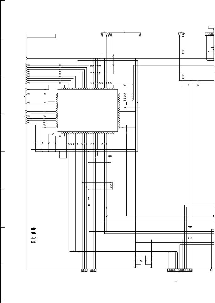
CD-C440W/CP-C440W
A |
|
|
|
|
|
|
|
|
|
|
|
|
|
|
|
|
|
|
|
|
|
|
|
|
|
|
|
|
|
|
|
|
|
|
|
|
|
|
|
|
|
|
|
|
|
|
|
|
|
|
|
|
|
|
|
|
|
|
|
|
|
P18 5 |
||
|
|
|
|
|
|
|
|
|
|
|
|
|
|
|
|
|
|
|
|
|
|
|
|
|
|
|
|
|
|
|
|
|
|
|
|
|
|
|
|
|
|
|
|
|
|
|
|
|
|
|
|
|
|
|
|
|
|
|
|
|
TO DISPLA |
|||
|
|
|
|
|
|
|
|
|
|
|
|
|
|
|
|
|
|
|
|
|
|
|
|
|
|
|
|
|
|
|
|
|
P17 7-H |
|
|
|
|
P23 12-C |
|
|
|
|
|
|
|
|
|
|
P23 12-D |
|
|
|
|
|
|
FW70 |
||||||||
|
|
|
|
|
|
|
|
|
|
|
|
|
|
|
|
|
|
|
|
|
|
|
|
|
|
|
|
|
|
|
|
|
|
|
|
|
|
|
|
|
|
|
|
|
|
|
|
|
|
|
|
|
|
|
||||||||||
|
|
|
|
|
|
|
|
|
|
|
|
|
|
|
|
|
|
|
|
|
|
|
|
|
|
|
|
|
|
TO CD SECTION |
|
TO DECK SECTION |
|
|
|
|
|
|
|
|
TO DECK SECTION |
|
|
|
|
|||||||||||||||||||
|
|
|
|
MAIN PWB-A1(2/3) |
|
|
|
|
|
|
|
|
|
|
|
|
|
|
|
|
|
|
|
|
|
|
|
|
21 |
18 |
42 |
43 |
|
|
|
|
|
|
40 |
|
|
|
|
|
|
|
|
|
30 |
29 |
|
|
|
|
WT502 |
1 |
2 |
3 |
4 |
|||||
|
|
|
|
|
|
|
|
|
|
|
|
|
|
|
|
|
|
|
|
|
|
|
|
|
|
|
|
|
|
|
|
|
|
|
|
|
|
|
|
|
|
|
|
|
|
|
|
|
|
|
|
|
|
|
|
|
|
|
|
|||||
B |
12-G |
SECTION |
|
|
|
|
|
|
|
|
|
|
|
|
|
|
|
|
|
|
|
|
|
|
|
|
|
|
|
|
|
|
CD PUIN |
|
CD DRF |
F.A.S. |
RUN PULSE |
|
|
|
|
|
|
CAM SW |
|
|
|
|
|
|
|
|
REC L-CH |
REC R-CH |
|
|
|
|
|
CLK |
DO |
DI |
CE |
|
P23 |
DECK |
|
|
|
|
|
|
|
|
|
|
|
|
|
|
|
|
|
|
|
|
|
|
|
|
|
|
|
|
|
|
|
|
|
|
|
|
R55 |
|
|
|
|
|
|
|
|
|
|
|
|
|
|
|
|
|
|
|
|
|
|
|
|
|
|
|
|
|
11 |
D_GND |
|
|
|
|
|
|
|
|
|
|
|
|
|
|
|
|
|
|
|
|
|
|
|
|
|
|
|
|
|
|
|
|
|
|
10K |
|
|
|
|
|
|
|
|
|
|
|
|
|
|
|
|
|
|
|
|
|
|
|
|
|
|
H-7P17 |
SECTIONCDTOTO |
|
|
|
|
|
|
|
|
|
|
|
|
|
|
|
|
|
CQCKCD |
COINCD |
SQOUTCD |
WRQCD |
RWCCD |
C6031KR613SCKMAIN150P |
C6051KR614SOMAIN150P |
C6041KR615SIMAIN150P |
CLEAR1KR616C606150P |
|
1KR617C607STBMAIN150P |
1KR618 |
GNDD |
1KR620 |
1KR621F.A.S. |
1KR622PULSERUN |
|
|
|
|
|
|
|
|
|
|
|
|
|
|
|
|
|
|
|
|
|
|
|
|
|
|
|
||
|
14 |
CD_RWC |
|
R602 |
R612 |
1K |
|
|
|
RESCD |
|
SL–CD |
SL+CD |
|
VDD |
|
|
R680 |
R623 |
|
|
|
|
|
|
|
|
|
|
|
|
|
|
|
|
|
R219 |
|
|
|
|
|||||||||||||||||||||||
|
|
|
CD_WRQ |
|
|
|
R611 |
1K |
|
|
|
|
|
|
|
|
|
|
|
|
|
|
|
|
|
|
|
|
|
|
|
|
|
|
|
10K |
|
|
|
|
|
|
|
|
|
|
|
|
|
|
|
|
|
|
|
|
|
|
|
|
|
|||
|
|
|
13 |
|
|
|
|
|
|
|
|
|
|
|
|
|
|
|
|
|
|
|
|
|
|
|
|
|
|
|
|
|
|
|
|
|
|
|
|
|
|
|
|
|
|
|
|
|
|
|
|
|
|
|
|
|
|
|
||||||
|
|
|
CD_SQIN |
|
|
|
R610 |
1K |
|
|
|
|
|
|
|
|
|
|
|
|
|
|
|
|
|
|
|
|
|
|
|
|
|
|
|
|
|
|
|
|
|
|
|
|
|
|
|
|
|
|
|
|
|
|
|
|
|
|
|
|
|
|||
|
|
|
17 |
|
|
|
|
|
|
|
|
|
|
|
|
|
|
|
|
|
|
|
|
|
|
|
|
|
|
|
|
|
|
|
|
|
|
|
|
|
|
|
|
|
|
|
|
|
|
|
|
|
|
|
|
|
|
|
|
|||||
|
|
|
CD_COOUT |
|
|
|
R609 |
1K |
|
|
|
|
|
|
|
|
|
|
|
|
|
|
|
|
|
|
|
|
|
|
|
|
|
|
|
|
|
|
|
|
|
|
|
|
|
|
|
|
|
|
|
|
|
|
|
|
|
|
|
|
|
|||
|
|
|
16 |
|
|
|
|
|
|
|
|
|
|
|
|
|
|
|
|
|
|
|
|
|
|
|
|
|
|
|
|
|
|
|
|
|
|
|
|
|
|
|
|
|
|
|
|
|
|
|
|
|
|
|
|
|
|
|
|
|||||
|
|
|
CD_CQCK |
|
|
|
R608 |
1K |
|
|
|
|
|
|
|
|
|
|
|
|
|
|
|
|
|
|
|
|
|
|
|
|
|
|
|
|
|
|
|
|
|
|
|
|
|
|
|
|
|
|
|
|
|
|
|
|
|
|
|
|
|
|||
|
|
|
15 |
|
|
|
|
|
|
|
|
|
|
|
|
|
|
|
|
|
|
|
|
|
|
|
|
|
|
|
|
|
|
|
|
|
|
|
|
|
|
|
|
|
|
|
|
|
|
|
|
|
|
|
|
|
|
|
|
|||||
|
|
|
CD_SL+ |
|
|
|
R607 |
1K |
|
|
|
|
|
|
|
|
|
|
|
|
|
|
|
|
|
|
|
|
|
|
|
|
|
|
|
|
|
|
|
|
|
|
|
|
|
|
|
|
|
|
|
|
|
|
|
|
|
|
|
|
|
|||
|
|
|
19 |
|
|
|
|
|
|
|
|
|
|
|
|
|
|
|
|
|
|
|
|
|
|
|
|
|
|
|
|
|
|
|
|
|
|
|
|
|
|
|
|
|
|
|
|
|
|
|
|
|
|
|
|
|
|
|
|
|||||
|
|
|
CD_SL– |
|
|
|
R606 |
1K |
|
|
|
|
|
|
|
|
|
|
|
|
|
|
|
|
|
|
|
|
|
|
|
|
|
|
|
|
|
|
|
|
|
|
|
|
|
|
|
|
|
|
|
|
|
|
|
|
|
|
|
|
|
|||
|
|
|
20 |
|
|
|
|
|
|
|
|
|
|
|
|
|
|
|
|
|
|
|
|
|
|
|
|
|
|
|
|
|
|
|
|
|
|
|
|
|
|
|
|
|
|
|
|
|
|
|
|
|
|
|
|
|
|
|
|
|||||
|
|
|
CD_RES |
|
|
|
R605 |
1K |
|
|
|
|
|
|
|
|
|
|
|
|
|
|
|
|
|
|
|
|
|
|
|
|
|
|
|
|
|
|
|
|
|
|
|
|
|
|
|
|
|
|
|
|
|
|
|
|
|
|
|
|
|
|||
|
|
|
12 |
|
|
|
|
|
|
|
|
|
|
|
|
|
|
|
|
|
|
|
|
|
|
|
|
|
|
|
|
|
|
|
|
|
|
|
|
|
|
|
|
|
|
|
|
|
|
|
|
|
|
|
|
|
|
|
|
|||||
|
|
|
CD_MUT |
|
|
|
R604 |
1K CD MUT |
|
|
|
|
|
|
|
|
|
|
|
|
|
|
|
|
|
|
|
|
|
|
|
|
|
|
|
|
|
|
|
|
|
|
|
|
|
|
|
|
|
|
|
|
|
R218 |
|
|
|
|
||||||
|
|
|
3 |
|
|
|
|
|
|
|
|
|
|
|
|
|
|
|
|
|
|
|
|
|
|
|
|
|
|
|
|
|
|
|
|
|
|
|
|
|
|
|
|
|
|
|
|
|
|
|
|
|
|
|
|
|||||||||
|
|
|
|
|
|
|
REC/P.B. |
|
|
|
|
|
|
|
|
|
|
|
|
|
|
|
|
|
|
|
|
|
|
|
|
|
|
|
|
|
|
|
SPE5 |
|
|
|
|
|
|
|
|
|
|
|
|
|
|
|
|
|
1K |
|
|
|
|
|||
|
|
|
|
|
|
|
|
|
|
|
|
|
|
|
|
|
|
|
|
|
|
|
|
|
|
|
|
|
|
|
|
|
|
|
|
|
|
|
|
|
|
|
|
|
|
|
|
|
|
|
|
|
|
|
|
|
|
|
|
|||||
|
|
SECTIONDECK |
|
REC/PB |
|
|
1K |
|
|
|
1 |
P93/FIP5 2 P92/FIP4 3 |
P91/FIP3 4 P90/FIP2 5 |
P81/FIP1 6 P80/FIP0 7 |
VDD 8 |
P27/SCK0 9 |
P26/SO0/SB110 |
P25/SI0/SB011 |
P24/BUSY 12 |
P23/STB 13 |
P22/SCK1 14 |
P21/SO1 15 |
P20/SI1 16 |
|
RESET 17 |
P74 18 |
P73 19 |
AVSS 20 |
P17/ANI7 21 |
P16/ANI6 22 |
P15/ANI5 23 |
24 |
|
|
1K |
|
|
|
|
|
|
|
|
|
|
|
|
|
|
|
|
|
|
1K |
|
|
|
|
||||||
|
12P23-D |
23 |
|
|
HI BSPEED |
76 |
|
|
|
29 |
|
|
|
SW |
|
|
|
|
|
|
|
|
|
|
|
|
|
|
|
|
|
|
|
|
||||||||||||||||||||||||||||||
|
HI_SPEED |
|
|
1K |
P101/ |
|
AVDD |
|
|
|
|
|
|
|
|
|
|
|
|
|
|
|
|
|
|
|
|
|
|
|
||||||||||||||||||||||||||||||||||
|
|
|
22 |
|
|
|
|
|
79 |
P96/ P94/FIP6 |
|
|
|
|
|
|
|
|
|
|
|
|
|
|
|
|
|
|
|
|
|
|
|
|
|
|
P14/ANI4 |
P12/ |
26 |
R625 |
1K SPE3 |
|
|
|
|
|
|
|
|
|
|
|
|
|
|
|
|
|
|
|
|
|
|
|
|
|
|
|
|
|
R671 |
|
|
|
|
|
|
|
|
|
|
|
|
|
|
|
|
|
|
|
|
|
|
|
|
|
|
|
|
|
|
|
|
|
|
|
|
|
|
|
|
|
|
|
|
|
|
|
|
|
|
|
|
|
|
|
|
|
|
|
|
|
26 |
REC_MUTE |
|
|
1K |
REC MUTE |
80 |
P95/ |
|
|
|
|
|
|
|
|
|
|
|
|
|
|
|
|
|
|
|
|
|
|
|
|
|
|
|
P13/ |
25 |
R624 |
1K SPE4 |
|
|
|
|
|
|
|
|
|
|
|
|
|
|
|
|
|
|
|
|
|
|
|
C |
|
|
|
|
|
|
|
|
|
FIP7 |
|
|
|
|
|
|
|
|
|
|
|
|
|
|
|
|
|
|
|
|
|
|
|
|
|
|
|
ANI3 |
|
|
|
|
|
|
|
|
|
|
|
|
|
|
|
|
|
|
|
|
|
|
|
|
|
|
|
|
|
|
|
|
|
|
|
FIP8 |
|
|
|
|
|
|
|
|
|
|
|
|
|
|
|
|
|
|
|
|
|
|
|
|
|
|
|
ANI2 |
|
R626 |
1K SPE2 |
|
|
|
|
|
|
|
|
|
|
|
|
|
|
|
|
|
|
|
|
|
|
||
|
|
|
|
|
|
|
|
|
78 |
FIP9P97/ |
|
|
|
|
|
|
|
|
|
|
|
|
|
|
|
|
|
|
|
|
|
|
|
|
|
P11/ANI1 |
27 |
|
|
|
|
|
|
|
|
|
|
|
|
|
|
|
|
|
|
|
|
|
|
|||||
|
|
|
|
|
|
R667 |
|
|
|
|
|
|
|
|
|
|
|
|
|
|
|
|
|
|
|
|
|
|
|
|
|
|
R627 |
1K SPE1 |
|
|
|
|
|
|
|
|
|
|
|
|
|
|
|
|
|
|
|
|
|
|
||||||||
|
|
|
|
|
|
|
77 |
FIP10P100/ |
|
|
|
|
|
|
|
|
|
|
|
|
|
|
|
|
|
|
|
|
|
|
|
|
|
P10/ANI0 |
28 |
|
|
|
|
|
|
|
|
|
|
|
|
|
|
|
|
|
|
|
|
|
|
|||||||
|
|
|
|
|
|
|
|
|
|
|
|
|
|
|
|
|
|
|
|
|
|
|
|
|
|
|
|
|
|
|
|
|
|
|
|
|
|
|
|
|
|
|
|
|
|
|
|
|
|
|
|
|
|
|
|
|||||||||
|
|
TO |
|
|
|
|
|
|
|
FIP11 |
|
|
|
|
|
|
|
|
|
|
|
|
|
|
|
|
|
|
|
|
|
|
|
|
|
|
|
|
|
|
|
|
CAM |
|
|
|
|
|
|
|
|
|
|
|
|
|
|
|
|
|
|
|
|
|
|
|
|
|
|
|
|
|
|
FIP12 |
|
|
|
|
|
|
|
|
|
|
|
|
|
|
|
|
|
|
|
|
|
|
|
|
|
|
|
|
|
|
|
|
|
|
|
|
|
|
|
|
|
|
|
|
|
|
|
|
|
|
|
|
|||
|
|
|
|
|
|
|
|
|
75 |
P102/ |
|
|
|
|
|
|
|
|
|
|
|
|
|
|
|
|
|
|
|
|
|
|
|
|
|
|
AVREF |
30 |
R633 |
1K |
|
|
|
|
|
|
|
|
|
|
|
|
|
|
|
|
|
|
|
|
|
|
||
|
|
|
|
|
|
|
|
|
74 |
P103/ |
|
|
|
|
|
|
|
|
|
|
|
|
IC601 |
|
|
|
|
|
|
|
|
|
|
P04/XT1 |
31 |
|
|
|
|
|
|
|
|
|
|
|
|
|
|
|
|
|
|
|
|
|
|
|||||||
|
|
|
|
|
|
R663 |
|
|
FIP13 |
|
|
|
|
|
|
|
|
|
|
|
|
|
|
|
|
|
|
|
|
|
|
|
|
|
|
|
|
|
|
|
|
|
|
|
|
|
|
|
|
|
|
|
|
|
|
|
|
|
||||||
|
|
SECTION |
|
|
|
BIAS |
73 |
P104/ |
|
|
|
|
|
|
|
|
|
|
IX0171AW |
|
|
|
|
|
|
|
|
|
XT2 |
32 |
|
D_GND |
|
|
|
|
|
|
|
|
|
|
|
|
|
|
|
|
|
|
|
|
|
|||||||||||
|
D-12 |
32 |
|
R661 |
1K |
72 |
P105/ |
|
|
|
|
|
|
|
|
|
|
|
|
|
|
|
|
|
|
|
VSS |
33 |
|
|
|
|
|
|
|
|
|
|
|
|
|
|
|
|
|
|
|
|
|
|
||||||||||||||
|
25 |
|
P.B.MUTE |
69 |
P107/ |
|
|
|
|
|
|
|
|
|
|
|
|
|
|
|
|
|
|
|
|
|
|
|
|
|
|
|
P37 |
36 |
|
|
|
|
|
|
|
|
|
|
|
|
|
|
|
|
|
|
|
|
|
|
|
|
||||||
|
|
|
|
|
|
1K |
|
|
FIP14 |
|
|
|
|
|
|
|
|
|
|
|
|
|
|
|
|
|
|
|
|
|
|
|
|
|
|
|
|
|
|
|
|
|
|
|
|
|
|
|
|
|
|
|
|
|
|
|
|
|
|
|
|
|
||
|
|
|
|
D_GND |
|
|
|
GND |
|
FIP15 |
|
|
|
|
|
SYSTEM MICROCOMPUTER |
|
|
|
X1 |
|
|
|
|
|
|
|
|
|
|
|
|
|
|
|
|
|
|
|
|
|
|
|
|
|
|||||||||||||||||||
|
|
|
|
R662 |
12K |
71 VLOAD |
|
|
|
|
|
|
|
|
34 |
|
|
|
|
|
|
|
|
|
|
|
|
|
|
|
|
|
|
|
|
|
|
|
|
|||||||||||||||||||||||||
|
|
|
24 |
|
T1/T2 |
70 |
P106/ |
|
|
|
|
|
|
|
|
|
|
|
|
|
|
|
|
|
|
|
|
|
|
|
|
|
|
|
X2 |
35 |
|
|
|
|
|
|
|
|
|
|
|
|
|
|
|
|
|
|
|
|
|
|
|
|
||||
|
|
|
|
|
|
|
|
|
|
FIP16 |
|
|
|
|
|
|
|
|
|
|
|
|
|
|
|
|
|
|
|
|
|
|
|
|
|
|
|
|
|
|
|
|
|
|
|
|
|
|
|
|
|
|
|
|
|
|
|
|
|
|
|
|
|
|
|
P23 |
TO DECK |
|
REC RVS |
R660 |
1K |
REC RVS |
|
FIP17 |
|
|
|
|
|
|
|
|
|
|
|
|
|
|
|
|
|
|
|
|
|
|
|
|
|
|
|
|
|
|
|
|
|
|
|
|
|
|
|
|
|
|
|
|
|
|
|
|
|
|
|
|
|
||
|
44 |
68 |
P110/ |
|
|
|
|
|
|
|
|
|
|
|
|
|
|
|
|
|
|
|
|
|
|
|
|
|
|
P36/BUZ |
37 |
|
|
|
|
|
|
|
|
|
|
|
|
|
|
|
|
|
|
|
|
|
|
|
|
|||||||||
|
|
REC FWD |
R659 |
1K |
REC FWD |
|
FIP18 |
|
|
|
|
|
|
|
|
|
|
|
|
|
|
|
|
|
|
|
|
|
|
|
|
|
|
|
|
|
|
|
|
|
|
|
|
|
|
|
|
|
|
|
|
|
|
|
|
|
|
|
|
|
||||
|
39 |
67 |
P111/ |
P115/ FIP23 P116/ FIP24 |
P117/ FIP25 P120/ FIP26 |
P121/ FIP27 P122/ FIP28 |
P123/ FIP29 |
P124/ FIP30 |
P125/ FIP31 P126/ FIP32 |
P127/ FIP33 |
VDD |
P70 |
|
P71 |
P72 |
|
IC |
P00/INTP0/TI0 |
P01/INTP1 |
P02/INTP2 |
P03/INTP3/CI0 |
P30/TO0 |
P31/TO1 |
P35/PCL |
38 |
|
|
|
|
|
|
|
|
|
|
|
|
|
|
|
|
|
|
|
|
|
|
|
|
|||||||||||||||
|
|
|
|
|
|
|
|
|
P114/ FIP22 |
|
|
P32/TO2 |
|
|
|
|
|
|
|
|
|
|
|
|
|
|
|
|
|
|
|
|
|
|
|
|
|
|
||||||||||||||||||||||||||
|
|
|
|
|
R658 |
1K |
|
|
FIP19 |
|
|
|
|
|
|
|
|
|
|
|
|
|
|
|
|
|
|
|
|
|
|
|
|
|
|
|
|
39 SYS MUTE |
|
|
|
|
|
|
|
|
|
|
|
|
|
|
|
|
|
|
|
|
|
|
||||
|
|
|
|
|
|
66 |
P112/ |
|
|
|
|
|
|
|
|
|
|
|
|
|
|
|
|
|
|
|
|
|
|
|
|
|
|
P34/TI2 |
|
|
|
|
|
|
|
|
|
|
|
|
|
|
|
|
|
|
|
|
|
|
||||||||
|
|
|
|
|
R657 |
1K |
|
|
FIP20 |
|
|
|
|
|
|
|
|
|
|
|
|
|
|
|
|
|
|
|
|
|
|
|
|
|
|
|
P33/ |
|
MIC |
|
|
|
|
|
|
|
|
|
|
|
|
|
|
|
|
|
|
|
|
|
|
|
||
|
|
|
|
|
|
|
|
|
65 |
FIP21 |
|
|
|
|
|
|
|
|
|
|
|
|
|
|
|
|
|
|
|
|
|
|
|
|
|
|
|
TI1 |
40 |
R632 |
|
|
|
|
|
|
|
|
|
|
|
|
|
|
|
|
|
|
|
|
|
|
|
|
|
|
|
|
|
|
|
|
|
|
|
|
|
|
|
|
|
|
|
|
|
|
|
|
|
|
|
|
|
|
|
|
|
|
|
|
|
|
|
|
|
|
|
|
|
|
|
|
|
|
|
|
|
|
|
|
|
|
|
|
|
|
|
|
|
|
|
|
|
|
|
|
|
|
|
|
|
|
|
|
|
|
|
|
|
|
|
|
|
|
|
|
|
|
|
|
|
|
|
|
|
|
|
|
|
|
1K |
|
|
|
|
|
|
|
|
|
|
|
|
|
|
|
|
|
|
|
|
|
|
|
D |
|
|
|
|
|
|
|
|
|
|
64 |
63 |
62 |
|
61 |
60 |
|
59 |
58 |
57 |
56 |
55 |
54 |
53 |
52 |
51 |
|
50 |
49 |
48 |
47 |
46 |
45 |
44 |
43 |
42 |
41 |
|
|
|
R628 |
|
|
|
|
|
|
|
|
|
|
|
|
|
|
|
|
|
|
|
|
|
|
|
|
|
|
|
|
|
|
|
|
|
|
|
|
|
|
|
1K |
|
|
|
|
|
|
|
|
|
|
|
|
|
|
|
|
|
|
|
|
|
|
||||||||||||||||||||||||||
|
|
|
|
|
|
|
|
|
|
|
SPAN9K |
|
PASSSRS |
SRS3D |
|
SRSA |
SRSB |
|
INHSRS |
|
SWU/DCD |
D.NO.CDSW |
SWO/CCD |
VDD |
SWMOTTA |
SOLTA |
SPEEDF/R |
VSS |
|
|
DRVRLY |
POWER |
DETSP |
CLK |
DATA |
ENEBLE |
|
|
|
|
|
|
|
|
|
|
|
|
|
|
|
|
|
|
|
|
|
|
|
|
|
|||
|
|
|
|
|
|
|
R656 |
|
|
|
|
|
|
|
|
|
|
|
|
|
|
|
|
|
|
|
|
|
|
|
|
|
|
|
|
|
|
|
|
|
|
|
||||||||||||||||||||||
|
|
|
|
|
|
|
|
1K |
|
R655 |
|
|
|
|
|
|
|
|
|
|
|
|
|
|
|
|
|
|
|
|
|
|
|
|
|
|
|
|
|
|
|
|
|
|
|
|
|
|
|
|
|
|
|
|
|
|
|
|
|
|
|
|
|
|
|
|
|
|
|
|
|
|
|
|
|
|
|
|
|
|
|
|
|
|
|
|
|
|
|
|
|
|
|
|
|
|
|
|
|
|
|
|
|
|
|
|
|
|
|
|
|
|
|
|
|
|
|
|
|
|
|
|
|
|
|
|
|
||
|
|
|
|
|
|
|
|
|
|
1K |
|
|
|
|
|
|
|
|
|
|
|
|
|
|
|
|
|
|
|
|
|
|
|
|
|
|
|
|
|
|
|
|
|
|
|
|
|
|
|
|
|
|
|
|
|
|
|
|
|
|
|
|
|
|
|
|
|
|
R673 |
R672 |
R675 |
R674 |
|
1K |
1K |
1K |
1K |
1K |
1K |
1K |
1K |
1K |
|
1K |
1K |
|
|
|
|
1K |
1K |
1K |
|
|
|
|
|
|
|
|
|
|
|
|
|
|
|
|
|
|
|
|
|
|
|
|
|
|
|
|
|
||||||||
|
|
|
|
10K |
|
10K |
10K |
10K |
|
|
|
|
|
|
|
|
|
|
|
|
|
|
|
|
|
|
|
D GND |
|
|
|
|
|
|
|
|
|
|
|
|
|
|
|
|
|
|
|
|
|
|
|
|
|
|
|
|
|
|
|
|
|
|
||
|
|
|
|
|
|
|
|
|
|
|
|
R654 |
R653 |
R652 |
R651 |
R650 |
R649 |
R647 |
R646 |
R645 |
|
R643 |
R642 |
|
|
|
R638 |
R637 |
R636 |
|
|
|
|
|
|
|
|
|
|
|
|
|
|
|
|
|
|
|
|
|
|
|
|
|
|
|
|
|
||||||
|
|
|
|
|
|
|
|
|
|
|
R676 |
|
|
|
|
|
|
|
|
|
|
|
|
|
|
|
|
|
|
|
R679 |
10K |
|
|
|
|
C602 |
|
|
|
|
|
|
|
|
|
|
|
|
|
|
|
|
|
|
|
|
|
|
|
|
|
||
|
|
|
|
|
|
|
|
|
|
|
47K |
|
|
|
|
|
|
|
|
|
|
|
|
|
|
|
|
|
|
|
|
|
|
|
|
|
|
|
|
|
|
|
|
|
|
|
|
|
|
|
|
|
|
|
|
|
|
|
|
|
|
|||
|
|
|
|
|
|
|
|
|
|
|
|
|
|
|
|
|
|
|
|
|
|
|
|
|
|
|
|
|
|
R641 |
1K |
|
|
C601 |
220/10 |
|
0.022 |
|
|
|
|
|
|
|
|
|
|
|
|
|
|
|
|
|
|
|
|
|
|
|
|
|
||
|
|
|
|
|
|
|
|
|
|
|
|
|
|
|
|
|
|
|
|
|
|
|
|
|
|
|
|
|
|
|
|
|
|
|
|
|
|
|
|
|
|
|
|
|
|
|
|
|
|
|
|
|
|
|
|
|
|
|
|
|||||
|
|
|
|
|
|
|
|
|
|
|
|
|
|
|
|
|
|
|
|
|
|
|
|
|
+B |
|
|
|
|
|
|
|
|
|
|
|
|
|
|
|
|
|
|
|
|
|
|
|
|
|
|
|
|
|
|
|
|
|
|
|
|
|
|
|
E |
|
|
|
|
|
|
|
|
|
|
|
|
|
|
|
|
|
|
|
|
|
|
|
|
|
|
|
|
|
|
|
|
|
|
|
|
|
|
|
|
|
|
|
|
|
|
|
|
|
|
|
|
|
|
|
|
|
|
|
|
|
|
|
|
|
|
|
|
|
|
|
|
|
|
|
|
|
|
|
|
|
|
|
|
|
|
|
|
|
|
|
|
|
|
|
|
|
|
|
|
R640 |
|
|
|
|
|
|
|
|
|
|
|
|
|
|
|
|
|
|
|
|
|
|
|
|
|
|
||
|
|
|
|
|
|
|
|
|
|
|
|
|
|
|
|
|
|
|
|
|
|
|
|
|
|
|
|
|
|
|
|
|
|
|
|
10K |
|
|
|
|
|
|
|
|
|
|
|
|
|
|
|
|
|
|
|
|
|
|
|
|
|
|
||
|
|
|
|
|
|
|
|
|
|
|
|
|
|
|
|
|
|
|
|
|
|
|
|
|
|
|
|
|
|
|
|
|
|
|
|
|
|
R635 |
|
|
|
|
|
|
|
|
|
|
|
|
|
|
|
|
|
|
|
|
|
|
|
|
|
|
|
|
|
|
|
|
|
|
|
|
|
|
|
|
|
|
|
|
|
|
|
|
|
|
|
|
|
|
|
|
|
|
|
|
|
|
|
|
10K |
|
|
|
|
|
|
|
|
|
|
|
|
|
|
|
|
|
|
|
|
|
|
|
|
|
|
|
|
|
|
|
|
|
|
|
|
|
|
|
|
|
|
|
|
|
|
|
|
|
|
|
|
|
|
|
|
|
|
|
|
|
|
R634 |
|
|
|
|
|
|
|
|
|
|
|
|
|
|
|
|
|
|
|
|
|
|
|
|
|
|
||
|
|
|
|
|
|
|
|
|
|
|
|
|
|
|
|
|
|
|
|
|
|
|
|
|
|
|
|
|
|
|
|
|
|
|
|
10K |
|
|
|
|
|
|
|
|
|
|
|
|
|
|
|
|
|
|
|
|
|
|
|
|
|
|
|
|
|
|
|
|
|
|
|
|
|
|
|
|
|
|
|
|
|
|
|
|
|
|
|
|
|
|
L601 100 H |
|
|
|
|
|
|
|
|
|
|
|
|
|
|
|
|
|
|
|
|
|
|
|
|
|
|
|
|
|
|
|
|
|
|
|
|
|
|
|
|
|
|
|
|
|
|
|
|
|
|
|
|
|
|
|
|
|
|
|
|
|
|
|
|
D601 |
1SS133 |
|
|
|
|
|
|
|
|
R684 |
|
|
|
|
|
|
|
|
|
|
|
|
|
|
|
|
|
|
|
|
|
|
|
|
|
|
|
|
F |
|
|
|
|
|
|
|
|
|
|
|
|
|
|
|
|
|
|
|
|
|
|
|
|
|
|
|
|
|
|
|
|
|
|
|
10K |
|
|
|
|
|
|
|
|
|
|
|
|
|
|
|
|
|
|
|
|
|
|
|
|
|
|
|
|
|
|
|
|
|
|
|
|
|
|
|
|
|
|
|
|
|
|
|
|
|
|
|
|
|
|
|
|
|
|
|
|
|
|
|
|
|
|
|
|
|
|
|
|
|
|
|
|
|
|
|
|
|
|
|
|
|
|
|
|
|
|
|
|
|
|
|
|
|
|
|
|
|
|
|
|
|
|
|
|
|
|
|
|
|
|
|
|
|
|
|
|
|
|
|
|
|
|
|
|
|
D602 |
|
|
|
|
|
|
|
|
|
|
|
|
|
|
|
|
|
|
|
|
|
|
|
|
|
|
|
|
|
|
|
|
|
|
|
|
|
|
|
|
|
|
|
|
|
|
|
|
|
|
|
|
|
|
|
|
|
|
|
|
|
|
|
|
1SS133 |
|
|
|
|
|
|
|
|
|
|
|
|
|
|
|
|
|
|
|
|
|
|
|
|
|
D8 |
||
|
|
|
|
|
|
|
|
|
|
|
|
|
|
|
|
|
|
|
|
|
|
|
|
|
|
|
|
|
|
|
|
|
|
|
|
|
|
|
|
|
|
|
|
|
|
|
|
|
|
|
|
|
|
|
|
|
|
|
|
|
|
|
1SS |
|
|
|
|
|
|
|
|
|
|
|
|
|
|
|
|
|
|
|
|
|
|
|
|
|
|
|
|
|
|
|
|
|
|
|
|
|
|
|
|
|
|
|
|
|
|
|
|
|
|
|
|
|
|
|
|
|
|
C452 |
4.7/50 |
|
C451 |
|
|
|
|
|
|
|
|
FM SIGNAL |
|
|
|
|
|
|
|
|
|
|
|
|
|
|
|
|
|
|
|
|
|
|
|
|
|
|
|
|
|
|
|
|
|
|
|
|
|
|
|
|
|
|
|
|
|
|
|
|
|
|
|
4.7/50 |
|
|
|
|
||||
|
|
|
|
|
|
|
|
|
|
|
|
|
|
|
|
|
|
|
|
|
|
|
|
|
|
|
|
|
|
|
|
|
|
|
|
|
+B |
|
|
|
|
|
|
|
|
|
|
|
+B |
|
|
|
|
|
|
|
|
|
|
|||||
|
|
|
|
|
|
|
|
|
|
|
|
|
|
|
|
|
|
|
|
|
|
|
|
|
|
|
|
|
|
|
|
|
|
|
|
|
|
|
|
|
|
|
|
|
|
|
|
|
|
|
|
|
|
|
|
|
|
|
|
|
|
|
||
|
|
|
|
PLAYBACK SIGNAL |
|
|
|
|
|
|
|
|
|
|
|
|
+B |
|
|
|
|
|
|
|
|
|
|
|
|
|
|
|
|
|
|
|
|
|
|
|
|
|
|
|
|
|
|
|
|
|
|
|
|
|
|
|||||||||
|
|
|
|
|
|
|
|
|
|
|
|
|
|
|
|
|
|
|
|
|
|
|
|
|
|
|
|
|
|
|
|
|
|
|
|
|
|
|
|
|
|
|
|
|
|
|
|
R456 |
3.9K |
|
|
|
|
|
|
|||||||||
|
|
|
|
RECORD SIGNAL |
|
|
|
|
|
|
|
|
|
|
|
|
|
|
|
|
|
|
|
|
|
|
|
|
|
|
|
|
|
|
|
|
|
|
|
|
|
|
|
|
|
|
|
|
|
|
3.9K |
|
|
|
|
|||||||||
|
|
|
|
|
|
|
|
|
|
|
|
|
|
PASSSRS |
SRS/3D |
|
ASRS |
BSRS |
|
INHSRS |
|
|
|
|
|
|
|
|
|
|
|
|
|
|
|
|
|
|
|
|
|
|
|
|
|
|
|
|
|
|
|
|
|
|
|
|
|
|
|
R455 |
|
|
|
|
G |
|
|
|
CD SIGNAL |
|
|
|
|
|
|
|
|
|
|
|
|
|
|
|
|
|
|
|
|
|
|
|
|
|
|
|
|
|
|
|
|
|
|
|
|
|
|
|
+B |
|
|
|
|
|
|
|
|
|
|
||||||||||
|
|
|
|
|
|
|
|
|
|
|
|
|
|
|
|
|
|
|
|
|
|
|
|
|
|
|
|
|
|
|
|
|
|
|
|
|
|
|
|
|
|
|
|
|
|
|
|
|
|
|
|
|
|
|
|
|
|
|||||||
|
|
|
|
|
|
|
|
|
|
|
|
|
|
|
|
|
|
|
|
|
|
|
|
|
|
|
|
|
|
|
|
|
|
|
|
|
|
|
|
|
|
|
|
|
|
|
|
|
|
|
|
|
|
|
|
|
|
|
|
|
|
|
||
|
|
|
|
|
|
|
|
|
|
|
|
|
|
|
|
|
|
|
|
|
CD U/D |
CD D NO |
CD TRAYEND |
|
TA MOT SW |
SOLENOID |
TA MOT H/L |
|
|
|
|
|
|
|
|
|
|
|
|
D818 |
1SS133 |
D817 1SS133 |
D820 |
1SS133 |
D819 |
1SS133 |
SRS INH |
SRS B |
SRS A |
SRS/3D |
SRS PASS |
A 12V |
R OUT |
|
L OUT |
R IN |
|
L IN |
|
|
|
|
||
|
|
|
|
|
|
|
|
|
|
|
|
|
|
|
|
|
|
|
|
|
|
8 |
9 |
10 |
|
37 |
38 |
36 |
|
|
|
|
|
|
|
|
|
|
|
|
|
|
|
|
|
|
CNP501 |
10 |
9 |
8 |
7 |
6 |
5 |
4 |
3 |
2 |
1 |
|
|
7 |
||||
|
|
|
|
|
|
|
|
|
|
|
|
|
|
|
|
|
|
|
|
|
|
|
|
|
|
|
|
|
|
|
|
|
|
|
|
|
|
|
|
|
11 |
|
|
|||||||||||||||||||||
TO CD |
TO DECK |
|
INHSRS SRSB SRSA SRS/3D PASS 12VA |
GNDA OUTCH-R OUTCH-L CH-RIN |
CH-LIN |
TO CD/DE |
||
|
SECTIO |
|||||||
SECTION |
SECTION |
|
|
|
|
|
|
P17 12- |
P17 10-H |
P23 12-B |
|
|
|
|
|
|
P23 12- |
|
|
|
CNS501 |
|
|
|
|
|
|
|
|
|
|
|
|||
H |
|
TO |
SRS PWB |
|
|
|
||
|
|
P28 4-H |
|
|
|
|||
• NOTES ON SCHEMATIC DIAGRAM can be found on page 12.
|
1 |
2 |
3 |
4 |
5 |
6 |
Figure 20 SCHEMATIC DIAGRAM (5/14)
– 20 –
|
|
|
|
|
|
|
|
|
|
|
|
|
|
|
|
|
|
|
|
|
|
|
|
|
|
|
|
|
|
|
|
|
|
|
|
|
|
|
|
|
|
|
|
|
|
|
|
|
|
|
|
|
|
|
|
|
|
|
|
|
|
|
|
|
|
|
|
|
|
|
|
|
|
|
|
|
|
CD-C440W/CP-C440W |
||||||
|
|
P18 5-A |
|
|
|
|
|
|
|
|
|
|
|
|
|
P27 10-G |
|
|
|
|
|
|
|
|
|
|
|
|
|
|
|
|
|
|
|
|
|
|
|
|
|
|
|
|
|
|
|
|
|
|
|
|
|
|
|
|
|
|
|
|
|
|
|
|
|
|
|
|
|
|
|
|
|
|
|
|
||||||||
|
TO DISPLAY PWB |
|
|
|
|
|
|
|
|
|
TO TUNER PWB |
|
|
|
|
|
|
|
|
|
|
P17 12-C |
|
|
|
|
|
|
|
|
|
|
|
|
|
|
|
|
|
|
|
|
|
|
|
|
|
|
|
|
|
|
|
|
|
|
|
|
|
|
|
|
|
|
|
|||||||||||||||||||
|
|
|
FW702 |
|
|
|
|
|
|
|
|
|
|
|
|
|
CNP303 |
|
|
|
|
|
|
|
|
|
|
TO CD SECTION |
|
|
|
|
|
|
|
|
|
|
|
|
|
|
|
|
|
|
|
|
|
|
|
|
|
|
|
|
|
|
|
|
|
|
|
|
|
|
|
|
|
|||||||||||||||
|
|
|
|
|
|
|
|
|
|
|
|
|
|
|
|
|
|
|
|
|
|
|
|
|
|
|
|
|
|
|
|
P23 12-D |
|
|
|
|
P23 12-D |
|
|
|
|
|
|
|
|
|
|
|
|
|
|
|
|
|
|
|
|
|
|
|
|
|
|
|
|
|
|
|
|
|
|
|
|
|
||||||||||
|
|
|
|
|
|
|
|
|
|
|
|
|
|
|
|
|
|
|
|
|
|
|
|
|
|
|
|
|
|
|
TO DECK |
|
|
|
|
TO DECK |
|
|
|
|
|
|
|
|
|
|
|
|
|
|
|
|
|
|
|
|
|
|
|
|
|
|
|
|
|
|
|
|
|
|
|
|
|
|||||||||||
WT502 |
|
|
|
|
|
|
|
|
|
CNP502 |
|
|
|
|
|
|
|
|
|
|
|
|
|
|
|
|
|
|
SECTION |
|
|
|
|
SECTION |
|
|
|
|
|
|
|
|
|
|
|
|
|
|
|
|
|
|
|
|
|
|
|
|
|
|
|
|
|
|
|
|
|
|
|
|
|
|||||||||||||
1 |
2 |
3 |
4 |
5 |
6 |
7 |
|
|
1 |
2 |
|
3 |
4 |
5 |
6 |
|
7 |
8 |
9 |
10 |
11 |
12 |
|
|
|
|
|
27 |
|
1 |
2 |
4 |
|
28 |
|
|
|
|
|
|
|
|
|
|
|
|
|
|
|
|
|
|
|
|
|
|
|
|
|
|
|
|
|
|
|
|
|
|
|
|
|
|
|
|
|
|||||||||
|
|
|
|
|
|
|
|
|
|
|
|
|
|
|
|
|
|
|
|
|
|
|
|
|
|
|
|
|
|
|
|
|
|
|
|
|
|
|
|
|
|
|
|
|
|
|
|
|
|
|
|
|
|
|
|
|
|
|
|
|
|
|
|
|
|
|
|
|
|
|
|
|
|
|
|
|
|
|
|
R561 |
|
|
|
|
|
CLK |
DO |
DI |
CE |
TUN MUTE |
TUN SD |
TUN SM |
|
|
|
|
|
D GND |
CLK |
DO |
|
CE |
DI |
|
A 12V |
A GND |
TUN MUTE |
TUN L-CH |
TUN R-CH |
TUN SD TUN SM |
|
|
|
|
|
TAPE R-CH |
|
CD R-CH |
A GND CD L-CH |
|
|
TAPE L-CH |
|
|
|
|
|
|
|
|
|
|
|
|
|
|
|
|
|
|
|
|
|
|
|
|
|
|
|
|
|
|
|
|
|
|
|
|
|
27K |
|
|
L-CH |
||||||
|
|
|
|
|
|
|
|
|
|
|
|
|
|
|
|
|
|
|
|
|
|
|
|
|
|
|
|
|
|
|
|
|
|
|
|
|
|
|
|
|
|
|
|
|
|
|
|
|
|
R563 |
|
C585 |
|
|
||||||||||||||||||||||||||||||
|
|
|
|
|
|
|
|
|
|
|
|
|
|
|
|
|
|
|
|
|
|
|
|
|
|
|
|
|
|
|
|
|
|
|
|
|
|
|
|
|
|
|
|
|
|
|
|
|
|
|
|
|
|
|||||||||||||||||||||||||||||||
|
|
|
|
|
|
|
|
|
|
|
|
|
|
|
|
|
|
|
|
|
|
|
|
|
|
|
|
|
|
|
|
|
|
|
|
|
|
|
|
|
|
|
|
|
|
|
|
|
|
1.8K |
|
390P |
|
|
VIDEO/AUX 1 |
|||||||||||||||||||||||||||||
|
|
|
|
|
|
|
|
|
|
|
|
|
|
|
|
|
|
|
|
|
|
|
|
|
|
|
|
|
|
|
|
|
|
|
|
|
|
|
|
|
|
|
|
|
|
|
|
|
|
R564 |
|
C586 |
|
|
||||||||||||||||||||||||||||||
|
|
|
|
|
|
|
|
|
|
|
|
|
|
|
|
|
|
|
|
|
|
|
|
|
|
|
|
|
|
|
|
|
|
|
|
|
|
|
|
|
|
|
|
|
|
|
|
|
|
|
|
|
|
|||||||||||||||||||||||||||||||
|
|
|
|
|
|
|
|
|
|
|
|
|
|
|
|
|
|
|
|
|
|
|
|
|
|
|
|
|
|
|
|
|
|
|
|
|
|
|
|
|
|
|
|
|
|
|
|
|
|
1.8K |
|
390P |
|
|
R-CH |
|||||||||||||||||||||||||||||
|
|
|
|
|
|
|
|
|
|
|
|
|
|
|
|
|
|
|
|
|
|
|
|
|
|
|
|
|
|
|
|
|
|
|
|
|
|
|
|
|
|
|
|
|
|
|
|
|
|
|
|
|
|
|
|
|
|
|
|
|
|
|
|
|
|
|
|
|
|
|
|
|
|
|
|
|
|
|
R562 |
|
|
|
||
|
|
|
|
|
|
|
|
|
|
|
|
|
|
|
|
|
|
|
|
|
|
|
|
|
|
|
|
|
|
|
|
|
|
|
|
|
|
|
|
|
|
|
|
|
|
|
|
|
|
|
|
|
|
|
|
|
|
|
|
|
|
|
|
|
|
|
|
|
|
|
|
|
|
|
|
|
|
|
R565 |
J501 |
||||
|
|
|
|
|
|
|
|
|
|
|
|
|
|
|
|
|
|
|
|
|
|
|
|
|
|
|
|
|
|
|
|
|
|
|
|
|
|
|
|
|
|
|
|
|
|
|
|
|
|
|
|
|
|
|
|
|
|
|
|
|
|
|
|
|
|
|
|
|
|
|
|
|
|
|
|
|
|
|
27K |
|||||
|
|
|
|
|
|
|
|
|
|
|
|
|
|
|
|
|
|
|
|
|
|
|
|
|
|
|
|
|
|
|
|
|
|
|
|
|
|
|
|
|
|
|
|
|
|
|
|
|
|
|
|
|
|
|
|
|
|
|
|
|
|
|
|
|
|
|
|
|
|
|
|
|
|
|
|
|
|
|
|
|
27K |
|
L-CH |
|
|
|
|
|
|
|
|
|
|
|
|
|
|
|
|
|
|
D502 1SS133 D501 1SS133 |
|
|
|
|
|
|
|
|
|
|
|
|
|
|
|
|
|
|
|
|
|
|
|
|
|
|
|
|
|
|
|
|
|
|
|
|
|
|
|
|
|
|
|
|
|
|
|
|
|
|
|
|
|
|
|
R567 |
|
|
|
|
|
|
|||||
|
|
|
|
|
|
|
|
|
|
|
|
|
|
|
|
|
|
|
|
|
|
|
|
|
|
|
|
|
|
|
|
|
|
|
|
|
|
|
|
|
|
|
|
|
|
|
|
|
|
|
|
|
|
|
|
|
|
|
|
|
|
|
|
|
|
|
|
|
|
|
|
|
C587 |
|
|
|
||||||||
|
|
|
|
|
|
|
|
|
|
|
|
|
|
C591 0.022 |
|
|
|
|
|
|
|
|
|
|
|
|
|
|
|
|
|
|
|
|
|
|
|
|
|
|
|
|
|
|
|
|
|
|
|
|
|
|
|
|
|
|
|
|
|
|
|
|
|
|
|
|
|
|
|
1.8K |
|
390P |
|
|
VIDEO/AUX 2 |
|||||||||
|
|
|
|
|
|
|
|
|
|
|
|
|
|
|
|
|
|
|
|
|
|
|
|
|
|
|
|
|
|
|
|
|
|
|
|
|
|
|
|
|
|
|
|
|
|
|
|
|
|
|
|
|
|
|
|
|
|
|
|
|
|
|
|
|
|
|
|
|
R568 |
|
C588 |
|
|
|||||||||||
|
|
|
|
|
|
|
|
|
|
|
|
|
|
|
|
|
|
|
|
|
|
|
|
|
|
|
|
|
|
|
|
|
|
|
|
|
|
|
|
|
|
|
|
|
|
|
|
|
|
|
|
|
|
|
|
|
|
|
|
|
|
|
|
|
|
|
|
|
|
|
|
|
||||||||||||
|
|
|
|
|
|
|
|
|
|
|
|
|
|
|
|
|
|
|
|
|
|
|
|
|
|
|
|
|
|
|
|
|
|
|
|
|
|
|
|
|
|
|
|
|
|
|
|
|
|
|
|
|
|
|
|
|
|
|
|
|
|
|
|
|
|
|
|
|
|
|
|
|
|
|
|
|
1.8K |
|
390P |
|
|
R-CH |
||
|
|
|
|
|
|
|
|
|
|
|
|
|
|
|
|
|
|
|
|
|
|
|
|
|
|
|
|
|
|
|
|
|
|
|
|
|
|
|
|
|
|
|
|
|
|
|
|
|
|
|
|
|
|
|
|
|
|
|
|
|
|
|
|
|
|
|
|
|
|
|
|
|
|
|
|
|
|
|
R566 |
|
|
|
||
|
|
|
|
|
|
|
|
|
|
|
|
|
|
|
|
|
|
|
|
|
|
|
|
|
|
|
|
|
|
|
|
|
|
|
|
|
|
|
|
|
|
|
|
|
|
|
|
|
|
|
|
|
|
|
|
|
|
|
|
|
|
|
|
|
|
|
|
|
|
|
|
|
|
|
|
|
|
|
|
|
|
|
||
|
|
|
|
|
|
|
|
|
|
|
|
|
|
|
|
|
|
|
|
|
|
|
|
|
|
|
|
|
|
|
|
|
|
|
|
|
|
|
|
|
|
|
|
|
|
|
|
|
|
|
|
|
|
|
|
|
|
|
|
|
|
|
|
|
|
|
|
|
|
|
|
|
|
|
|
|
|
|
27K |
|
|
D561 |
1SS133 |
|
|
|
|
|
|
|
|
|
|
|
|
|
|
|
|
|
|
|
|
|
|
|
|
|
|
|
|
|
|
C512 |
|
/501 |
|
1/50 |
/501 |
1/50 |
/501 |
1/50 |
|
/501 |
/501 |
|
/501 |
|
1/50 |
|
C511 |
|
|
|
|
|
|
|
|
|
|
|
|
|
|
|
|
|
|
|
|
|
|
|
|
|
|
|
|
C864 0.022 |
D560 |
1SS133 |
|
||||||
|
|
|
|
|
|
|
|
|
|
|
|
|
|
|
|
|
|
|
|
|
+B |
|
|
|
|
|
47/16 |
|
|
|
|
|
|
47/16 |
|
|
|
|
|
|
|
|
|
|
|
|
|
|
|
|
|
|
|
|
|
|
|
|
|
|
|
|
|
|||||||||||||||||||||
|
|
|
|
|
|
|
|
|
|
|
|
|
|
|
|
|
|
|
|
|
|
|
|
|
|
|
|
|
|
|
|
|
|
|
|
|
|
|
|
|
|
|
|
|
|
|
|
|
|
|
|
|
|
|
|
|
|
|
|
|
|
|
|
|
|
|||||||||||||||||||
|
|
|
|
|
|
|
|
|
|
|
|
|
|
|
|
|
|
|
|
|
|
|
|
|
|
|
|
|
R502 |
|
|
|
|
|
|
R501 |
|
|
|
|
|
|
|
|
|
|
|
|
|
|
|
|
|
|
|
|
|
|
|
|
|
|
|
|
|
|||||||||||||||||||
|
|
|
|
|
|
|
|
|
|
|
|
|
|
|
|
|
|
|
|
|
|
|
|
|
|
|
|
|
|
C510 |
|
C508 |
C506 |
C504 |
C502 |
C501 |
|
C503 |
C505 |
|
C507 |
|
C509 |
|
|
|
|
|
|
|
|
|
|
|
|
|
|
|
|
|
|
|
|
|
|
|
|
|
|
|
|
|
|
|
|
|
|
|
||||||
|
|
|
|
|
|
|
|
|
|
|
|
|
|
|
|
|
|
|
|
|
|
|
|
|
|
|
|
|
2.2K |
|
|
|
|
|
|
2.2K |
|
|
|
|
|
|
|
|
|
|
|
|
|
|
|
|
|
|
|
|
|
|
|
|
|
|
|
|
|
|
|
|
|
|
||||||||||||||
|
|
|
|
|
|
|
|
|
|
|
|
|
|
|
|
|
|
|
|
|
|
C515 |
R504 |
|
C514 100P |
|
|
|
|
|
|
|
|
|
C513 100P |
R503 |
|
|
|
|
|
|
|
|
|
|
|
|
|
|
|
|
|
|
|
|
|
|
|
|
|
|
|
|
|
|
|
|||||||||||||||||
|
|
|
|
|
|
|
|
|
|
|
|
|
|
|
|
|
|
|
|
|
|
|
|
1K |
|
1K |
1K |
1K |
1K |
|
|
|
|
|
|
|
|
|
|
|
|
|
|
|
|
|
|
|
|
|
|
|
|
|
|
|
|
|
|
|
|
|
|
|
|
|
|
|
|
|
|
|
||||||||||||
|
|
|
|
|
|
|
|
|
|
|
|
|
|
|
|
|
|
|
|
|
|
|
1/50 |
|
15K |
|
|
|
1K |
|
1K |
1K |
1K |
1K |
|
|
|
15K |
|
|
|
|
|
|
|
|
R532 |
C565 |
R531 |
|
|
|
|
|
|
|
|
|
|
|
|
|
|
|
|
|
||||||||||||||||||
|
|
|
|
|
|
|
|
|
|
|
|
|
|
|
|
|
|
|
|
|
|
C516 |
|
|
|
|
|
|
|
|
|
|
|
|
|
|
|
|
|
|
|
|
|
|
|
|
|
|
|
|
|
|
|
|
|
|
|
|
10K |
270P |
390K |
|
|
|
|
|
|
–B |
|
D551 |
|
|
|
|
|
|
||||||||
|
|
|
|
|
|
|
|
|
|
|
|
|
|
|
|
|
|
|
|
|
|
|
|
|
|
|
|
R520 |
|
R518 |
R516 |
R514 |
R512 |
R511 |
|
R513 |
R515 |
R517 |
R519 |
|
|
|
|
|
|
|
|
|
|
|
|
|
|
|
|
|
|
R534 |
|
|
|
|
|
|
|
|
|
|
|
|
||||||||||||||
|
|
|
|
|
|
|
|
|
|
|
|
|
|
|
|
|
|
|
|
|
|
|
1/50 |
|
|
|
|
|
|
|
|
|
|
|
|
|
|
|
|
|
|
C550 |
|
|
R533 |
|
C566 |
|
220K |
2 |
|
|
|
|
4 |
|
|
1SS133 |
|
SPE1 |
|
|
|
|||||||||||||||||||||
|
|
|
|
|
|
|
|
|
|
|
|
|
|
|
|
|
|
|
|
|
|
|
|
|
|
|
|
|
|
|
|
|
|
|
|
|
|
|
|
|
|
|
330/16 |
|
|
|
|
|
|
3 |
|
|
|
|
1 |
|
|
|
|
|
|
|
|
|
|
|||||||||||||||||||
|
|
|
|
|
|
|
|
|
|
|
|
|
+B |
|
|
|
|
|
|
|
|
|
|
|
|
|
|
|
|
|
|
|
|
|
|
|
+B |
|
|
|
|
|
|
|
|
|
|
|
|
|
|
|
|
|
|
|
|
|
|
33K |
|
270P |
|
R538 |
|
|
|
|
|
|
|
|
C576 |
|
R554 |
|
|
|
||||||
|
|
|
|
|
|
|
|
|
|
|
|
|
|
|
|
|
|
|
|
|
|
|
D557 |
1SS133 |
|
|
|
|
|
|
|
|
|
|
|
|
|
|
|
|
|
|
|
|
|
|
|
|
|
|
|
|
|
|
|
|
|
R537 |
39K |
C568 |
220K |
5 |
|
|
|
|
8 |
+B |
2.2/50 |
|
100K |
|
|
|
||||||||||
|
|
|
|
|
|
|
|
|
|
|
|
|
|
|
|
|
|
|
|
|
|
|
|
|
|
|
|
|
|
|
|
|
|
|
|
|
|
|
|
|
|
|
|
|
|
|
|
|
|
|
|
|
|
|
|
|
C549 |
|
|
|
|
680P |
|
|
|
|
|
|
|
|
|
|
|
SPE2 |
|
|
|
|||||||
|
|
|
|
|
|
|
|
|
|
|
|
|
|
|
|
|
|
|
|
|
|
|
|
|
|
|
|
|
|
|
|
|
|
|
|
|
|
|
|
|
|
|
|
|
|
|
|
|
|
|
|
|
|
|
|
|
|
|
|
|
|
|
|
|
|
|
6 |
|
|
|
|
7 |
|
|
|
|
|
|
|
|
|
|
||
|
|
|
|
|
|
|
|
|
|
|
|
|
|
|
|
|
|
|
|
|
|
|
|
C518 |
|
|
64 |
63 |
62 |
61 |
60 |
59 |
58 |
57 |
56 |
55 |
54 |
53 |
52 |
51 |
50 |
49 |
|
|
|
|
|
|
|
0.022 |
|
|
R536 |
12K |
|
|
|
R535 |
470K |
|
|
|
|
|
|
|
D552 1SS133 C577 |
|
R555 |
|
|
|
||||||||||||
|
|
|
|
|
|
|
|
|
|
|
|
|
|
|
|
|
|
|
|
|
|
|
|
1/50 |
|
|
|
|
|
|
|
|
|
|
0.0027 |
|
|
C567 |
|
|
|
|
|
|
|
|
|
|
|
|
|
|||||||||||||||||||||||||||||||||
|
|
|
|
|
|
|
|
|
|
|
|
|
|
|
|
|
|
|
|
|
|
|
|
|
|
RTIN |
|
RINVIN1 |
R5 |
R4 |
R3 |
R2 |
R1 |
VDD |
L1 |
L2 |
L3 |
L4 |
L5 |
LINVIN1 |
LSELO |
|
|
|
|
|
|
|
C569 |
|
|
|
|
|
IC502 |
|
|
|
|
100K |
|
|
|
|||||||||||||||||||||
|
|
|
|
|
|
|
|
|
|
|
|
|
|
|
|
|
|
|
|
|
|
|
C520 |
|
|
|
|
|
|
|
|
C517 |
|
|
|
|
|
680P |
|
|
|
|
|
|
|
|
|
|
||||||||||||||||||||||||||||||||||||
|
|
|
|
|
|
|
|
|
|
|
|
|
|
|
|
|
|
|
|
|
|
0.1/50 |
1 |
|
|
|
LTIN |
48 |
|
1/50 |
|
|
|
|
|
|
|
|
|
|
BA4558 |
|
|
|
2.2/50 |
|
|
|
|
|
|
|||||||||||||||||||||||||||||||||
|
|
|
|
|
|
|
|
|
|
|
|
|
|
|
|
|
|
|
|
|
|
|
C522 |
|
RF1C1 |
|
|
|
|
|
C519 |
|
|
|
R539 |
|
OPE AMP. |
|
|
|
|
|
|
|
|
|||||||||||||||||||||||||||||||||||||||
|
|
|
|
|
|
|
|
|
|
|
|
|
|
|
|
|
|
|
|
|
|
|
|
2 |
|
|
|
|
|
|
|
|
|
|
|
|
|
|
|
|
|
|
|
|
|
|
||||||||||||||||||||||||||||||||||||||
|
|
|
|
|
|
|
|
|
|
|
|
|
|
|
C528 C524 |
0.22/50 0.22/50 |
|
|
|
|
0.22/50 |
RF1C2 |
|
|
|
|
|
|
|
|
|
|
|
|
|
|
|
|
|
|
LF1C1 |
47 |
|
|
|
|
0.1/50 |
|
|
|
|
|
|
390K |
|
R542 |
|
|
|
|
|
–B |
|
|
D553 |
|
|
|
|
|
|
|||||||||||||
|
|
|
|
|
|
|
|
|
|
|
|
|
|
|
|
|
|
|
|
|
|
|
3 RF1C3 |
|
|
|
|
|
|
|
|
|
|
|
|
|
|
|
|
|
|
LF1C2 |
46 |
|
|
|
|
C521 |
|
|
|
R540 |
12K |
R541 |
22K 68K |
C570 0.0027 |
|
220K |
2 |
|
|
|
|
4 |
|
|
1SS133 |
|
SPE3 |
|
|
|
||||||||||||
|
|
|
|
|
|
|
|
|
|
|
|
|
|
|
|
|
0.068/63 |
|
|
|
|
4 |
RF2C1 |
|
|
|
|
|
|
|
|
|
|
|
|
|
|
|
|
|
|
LF1C3 |
45 |
|
|
|
|
0.22/50 |
|
|
|
|
|
3 |
|
|
|
|
1 |
|
|
|
|
R556 |
|
|
|
|||||||||||||||||
|
|
|
|
|
|
|
|
|
|
|
|
|
|
|
|
|
|
|
|
|
5 RF2C2 |
|
|
|
|
|
|
|
|
|
|
|
|
|
|
|
|
|
|
LF2C1 |
44 |
|
|
|
|
C523 |
|
|
|
|
R546 |
|
|
|
|
|
|
+B |
|
C578 |
|
|
|
|
||||||||||||||||||||
|
|
|
|
|
|
|
|
|
|
|
|
|
|
|
|
C526 |
|
|
|
|
6 RF2C3 |
|
|
|
|
|
|
|
|
|
|
|
|
|
|
|
|
|
|
LF2C2 |
43 |
|
|
|
|
0.22/50 |
|
|
R544 18K |
R545 |
|
220K |
5 |
|
|
|
|
8 |
2.2/50 |
|
100K |
|
|
|
||||||||||||||||||||
|
|
|
|
|
|
|
|
|
|
|
|
|
|
|
|
|
|
|
|
|
|
|
|
|
|
IC501 |
|
|
|
|
|
|
|
|
|
|
|
C525 |
|
|
|
|
|
|
|
|
|
|
|
|
|
|
SPE4 |
|
|
|
||||||||||||||||||||||||||||
|
|
|
|
|
|
|
|
|
|
|
|
|
|
|
|
|
|
|
|
7 |
RF3C1 |
|
|
|
|
|
|
|
|
|
|
|
|
|
LF2C3 |
42 |
|
|
|
|
0.068/63 |
|
|
|
|
|
R543 |
680K |
|
6 |
|
|
|
|
7 |
|
|
|
|
|
|
|
|
|
||||||||||||||||||||
|
|
|
|
|
|
|
|
|
|
|
|
|
|
|
|
|
|
|
|
8 |
RF3C2 |
|
|
|
|
|
LC75396E |
|
|
|
|
|
|
LF3C1 |
41 |
|
|
|
|
C527 |
|
|
|
|
|
|
|
|
|
|
|
|
|
|
D554 1SS133 C579 |
|
R557 |
|
|
|
||||||||||||||||||||||||
|
|
|
|
|
|
|
|
|
|
|
|
|
|
|
|
|
|
|
|
|
|
|
|
|
|
|
|
|
|
|
|
|
|
|
0.22/50 |
|
|
C571 |
|
|
|
IC503 |
|
|
|
100K |
|
|
|
|||||||||||||||||||||||||||||||||||
|
|
|
|
|
|
|
|
|
|
|
|
|
|
|
|
|
|
|
|
|
|
|
|
|
|
|
|
|
|
|
|
|
|
|
|
|
|
|
|
|
|
|
|
|
|
|
|
|
|
|
|
|
|
|||||||||||||||||||||||||||||||
|
|
|
|
|
|
|
|
|
|
|
|
|
|
|
|
|
|
|
|
9 |
RF3C3 |
|
|
|
AUDIO PROCES |
|
|
|
LF3C2 |
40 |
|
|
|
|
C529 |
|
|
|
0.0082 |
D556 |
|
BA4558 |
|
|
|
|
|
|
|
|
|
|||||||||||||||||||||||||||||||||
|
|
|
|
|
|
|
|
|
|
|
|
|
|
|
|
|
|
|
|
10 |
RF4C1 |
|
|
|
|
|
|
|
|
|
|
|
|
|
|
|
|
|
|
LF3C3 |
39 |
|
|
|
|
0.033/63 |
C572 |
|
0.0082 548R 56K |
|
|
|
|
2.2/50 |
|
|
|
|
|
|
||||||||||||||||||||||||
|
|
|
|
|
|
|
|
|
|
|
|
|
|
|
|
|
|
|
|
|
|
|
|
|
|
|
|
|
|
|
|
|
|
|
|
|
|
|
|
|
|
|
|
1SS133 OPE AMP. |
|
|
|
|
|
|
|
|||||||||||||||||||||||||||||||||
|
|
|
|
|
|
|
|
|
|
|
|
|
|
|
|
|
|
|
|
11 RF4C2 |
|
|
|
|
|
|
|
|
|
|
|
|
|
|
|
|
|
|
LF4C1 |
38 |
|
|
|
|
C531 |
|
|
|
|
|
|
|
|
|
|
|||||||||||||||||||||||||||||
|
|
|
|
|
|
|
|
|
|
|
|
|
|
C532 |
0.015/63 |
|
C534C530 0.00220.033/63 |
|
|
|
|
|
|
12 RF4C3 |
|
RFOUT |
|
|
|
|
|
|
|
|
|
|
|
|
|
|
|
|
LF4C2 |
37 |
|
|
|
|
0.015/63 |
|
|
|
|
|
|
R547 |
|
|
|
|
|
|
|
|
|
|
|
|
|
|
|
|||||||||||||
|
|
|
|
|
|
|
|
|
|
|
|
|
|
|
/63 |
|
|
|
|
|
RRIN |
|
|
|
|
|
|
|
|
|
|
|
|
|
|
|
|
|
|
C533 |
|
|
|
C573 |
|
2.2M |
|
|
|
|
|
|
|
|
|
|
|
|
|
|
|
|||||||||||||||||||||||
|
|
|
|
|
|
|
|
|
|
|
|
|
|
|
|
|
|
|
13 |
|
|
|
|
|
|
|
|
|
|
|
|
|
|
|
|
|
|
LF4C3 |
36 |
|
|
|
|
|
|
|
|
|
|
|
|
|
|
|
|
|
|
|
|
|
|
|
||||||||||||||||||||||
|
|
|
|
|
|
|
|
|
|
|
|
|
|
|
|
|
|
|
RF5 |
|
|
|
|
|
|
|
|
|
|
|
|
|
|
|
|
|
|
|
|
0.0022 /63 |
|
|
0.0068 |
R550 |
2 |
|
|
|
|
4 |
|
|
D555 |
|
|
|
|
|
|
|||||||||||||||||||||||||
|
|
|
|
|
|
|
|
|
|
|
|
|
|
|
|
|
|
|
14 |
RTOUT |
|
|
|
|
|
|
|
|
|
|
|
|
|
|
|
|
|
LF5 |
35 |
|
|
|
|
|
|
|
|
|
|
|
|
|
|
|
|
|
|
|
|
|
|
|
|
|||||||||||||||||||||
|
|
|
|
|
|
|
|
|
|
|
|
|
|
|
0.0047/63 |
|
|
|
|
|
|
|
|
|
|
15 RFIN |
17 |
18 |
|
|
|
|
|
|
|
|
|
|
|
|
|
|
LTOUT |
34 |
|
|
|
C535 |
0.0047 |
|
|
|
|
R549 |
C574 |
|
2.2M |
3 |
|
|
|
|
1 |
|
|
1SS133 |
|
SPE5 |
|
|
|
|||||||||||||
|
|
|
|
|
|
|
|
|
|
|
|
|
|
|
|
|
|
|
|
|
|
|
|
|
|
|
|
|
|
|
|
|
|
|
|
|
|
|
|
|
|
|
|
|
|
|
|
|
|
|
|
|
|
|
|
|
|
|
|
|
|
|
|
|
||||||||||||||||||||
|
|
|
|
|
|
|
|
|
|
|
|
|
|
|
|
|
|
|
|
|
|
|
|
|
16 RFCOM |
|
RRCOM |
RROUT |
RVREF |
|
|
|
|
|
|
LVREF |
LROUT |
LRCOM |
|
LFOUT |
LFCOM |
|
LFIN |
33 |
|
|
|
|
|
|
|
470K |
0.0068 |
|
|
|
|
|
|
|
|
|
|
|
C580 |
|
R558 |
|
|
|
||||||||||||||
|
|
|
|
|
|
|
|
|
|
|
|
|
|
|
|
|
|
|
|
|
|
C540 |
|
|
|
|
|
VREF |
CL |
|
CE |
VSS |
LRIN |
|
|
|
|
C537 |
|
|
|
|
|
|
|
|
|
C575 |
|
|
5 |
|
|
|
|
8 |
|
2.2/50 |
|
100K |
|
|
|
|||||||||||||||||||||
|
|
|
|
|
|
|
|
|
|
|
|
|
|
|
|
|
|
|
|
|
|
10/50 |
|
|
|
|
|
DI |
|
|
|
|
1/50 |
|
|
|
|
|
|
|
R553 |
0.022 |
|
|
|
|
|
|
|
+B |
|
|
|
|
|
|
|
|||||||||||||||||||||||||||
|
|
|
|
|
|
|
|
|
|
|
|
|
|
|
|
|
|
|
|
|
|
|
|
|
|
|
|
|
|
|
|
|
|
|
|
|
|
|
|
6 |
|
|
|
|
7 |
|
|
|
|
|
|
|
|
|||||||||||||||||||||||||||||||
|
|
|
|
|
|
|
|
|
|
|
|
|
|
|
|
|
|
|
|
|
|
|
|
|
|
|
|
17 |
18 |
19 |
20 |
21 |
22 |
23 |
24 |
25 |
26 |
27 |
28 |
29 |
30 |
31 |
32 |
|
|
|
|
|
|
|
|
|
|
|
|
|
270K |
|
|
|
|
|
|
|
|
|
|
|
|
|
|
|
|
|
|
|||||||||
|
|
|
|
|
|
|
|
|
|
|
|
|
|
|
|
|
|
|
|
|
|
|
|
|
|
|
|
|
|
|
|
|
|
|
|
|
|
|
|
|
|
|
|
|
|
|
|
|
|
|
|
|
|
|
|
|
|
|
|
|
||||||||||||||||||||||||
|
|
|
|
|
|
|
|
|
|
|
|
|
|
|
|
|
|
|
|
|
|
|
|
|
|
|
|
|
|
|
|
|
|
|
1K |
|
|
|
|
|
|
|
|
|
|
|
|
|
|
|
|
|
|
|
|
|
|
|
|
|
C583 |
R552 |
|
|
|
IC504 |
|
|
|
|
|
|
|
|
|
|
|
|||||||
|
|
|
|
|
|
|
|
|
|
|
|
|
|
|
|
|
|
|
|
|
|
|
|
|
C542 |
|
|
|
|
|
|
|
|
|
|
|
|
|
|
|
|
|
|
|
|
C539 |
|
|
|
|
|
|
|
|
|
|
0.022 |
560K |
|
|
BA4558 |
|
|
|
|
|
|
|
|
|
|
|
||||||||||||
|
|
|
|
|
|
|
|
|
|
|
|
|
|
|
|
|
|
|
|
|
|
|
|
|
2.2/50 |
|
|
|
|
|
|
|
R530 |
|
|
|
|
|
|
|
|
|
|
|
|
|
10/50 |
R570 |
|
|
|
R551 |
|
|
|
|
|
|
|
|
|
|
OPE AMP. |
|
|
|
|
|
|
|
|
|
|
|||||||||||
|
|
|
|
|
|
|
|
|
|
|
|
|
|
|
|
|
|
|
|
|
|
|
|
|
|
|
|
|
|
|
|
|
|
|
|
|
|
|
|
|
|
|
|
|
|
|
|
|
|
220K |
|
|
|
15K |
|
|
|
|
|
|
|
|
|
|
|
|
|
|
|
|
|
|
|
|
|
|
|
|
|
|
||||
|
|
|
|
|
|
|
|
|
|
|
|
|
|
C536 |
|
|
|
|
|
C538 1/50 |
|
|
|
|
|
|
C546 10/50 |
|
|
|
C553 47/16 |
ODR5291K |
ECR5281K |
|
|
|
C545 |
10/50 |
|
C541 2.2/50 |
|
|
|
|
|
|
|
R569 220K |
/63 |
|
|
|
|
|
|
|
|
|
|
|
|
|
|
|
|
–B |
C581 |
0.022 |
ZD551 MTZJ6.2C |
C582 |
0.022 |
|
|
|
|
|
||||||||
|
|
|
|
|
|
|
|
|
|
|
|
|
|
|
|
|
|
|
|
|
|
|
|
|
|
|
|
CLK |
|
|
|
|
|
|
|
|
|
R223 |
|
|
|
|
|
|
|
|
|
|
|
|
|
|
|
|
|
|
|
|
|
|
||||||||||||||||||||||||
|
|
|
|
|
|
|
|
|
|
|
|
|
|
|
|
|
|
|
|
|
|
|
|
|
|
|
|
|
|
|
|
C552 |
47/16 |
|
|
|
C551 |
47/16 |
|
|
|
|
|
|
|
|
|
|
|
|
|
|
|
|
|
|
|
|
|
|
|
|
|
|
|
|
|
|
|
|
|
|
|
|
|
|
|
|
|
|
||||
|
|
|
|
|
|
|
|
|
|
|
|
|
|
|
|
|
|
|
|
|
|
|
|
|
|
|
|
|
|
|
|
|
|
|
|
|
|
|
|
|
|
|
|
|
|
220K |
|
|
|
|
|
|
|
|
|
|
|
|
|
|
|
|
|
|
|
|
R560 |
|
R559 |
|
|
|
|
|
|
|
||||||||
|
|
|
|
|
|
|
|
|
|
|
|
|
|
|
|
|
|
|
|
|
|
|
|
|
|
|
|
|
|
|
|
|
|
|
|
|
|
|
|
|
|
|
|
|
|
|
|
|
|
|
|
|
|
|
|
|
|
|
|
|
|
|
|
|
|
|
330 |
|
330 |
|
|
|
|
|
|
|
||||||||
|
|
|
|
|
|
|
|
|
|
|
|
|
|
|
|
|
|
|
|
|
|
|
|
|
|
|
|
|
|
|
|
|
|
|
|
|
|
|
|
|
|
|
|
|
|
|
|
|
|
|
|
|
|
|
|
|
|
|
|
|
|
+B |
|
|
|
|
|
|
|
|
|
|
|
|
|
|
|
A_12V |
|
31 TO DECK |
||||
|
|
|
|
|
|
|
|
|
|
|
|
|
|
|
|
|
|
|
|
|
|
|
|
|
|
|
|
|
|
|
|
|
|
|
|
|
|
|
|
|
|
|
|
|
|
|
|
|
|
|
|
|
|
|
|
|
|
|
|
|
|
|
|
|
|
|
|
|
|
|
|
|
|
|
|
|
|
|
|
|
SECTION |
|||
|
|
|
|
|
|
|
|
|
|
|
|
|
|
|
|
|
|
|
|
|
|
|
|
|
|
|
|
|
|
|
|
|
|
|
|
|
|
|
|
|
|
|
|
|
|
|
|
|
|
C547 |
|
|
|
|
|
R574 |
|
|
|
|
|
|
|
|
|
|
|
|
|
|
|
|
|
|
|
|
|
|
|
P23 12-E |
||||
|
|
|
|
|
|
|
|
|
|
|
|
|
|
|
|
|
|
|
|
|
|
|
|
|
|
|
|
|
|
|
|
|
|
|
R510 |
|
R509 |
|
|
|
|
|
|
|
|
2.2/50 |
|
R507 |
|
|
2.2K |
|
|
|
|
|
|
|
|
|
|
|
|
|
|
|
|
|
|
|
|
|
|
|
|
|
|
|||||||
|
|
|
|
|
|
|
|
|
|
|
|
|
|
|
|
|
|
|
|
|
|
|
|
|
|
|
|
|
|
|
|
|
|
|
|
|
|
|
|
|
|
|
|
|
|
|
47K |
|
|
|
|
|
|
|
|
|
|
|
|
|
|
|
|
|
|
|
|
|
|
|
|
|
|
|
|
|
|
|
||||||
|
|
|
|
|
|
|
|
|
|
|
|
|
|
|
|
|
|
|
|
|
|
|
|
|
|
|
|
|
|
|
|
|
|
|
47K |
|
47K |
|
|
|
|
|
|
|
|
|
|
|
|
|
|
|
|
|
|
|
|
|
|
|
|
|
|
|
|
|
|
|
|
|
|
|
|
|
|
|
|
|
|
|
||||
|
|
|
|
|
|
|
|
|
|
|
|
|
|
|
|
|
|
|
|
|
|
|
|
|
|
|
R571 2.2K |
|
|
|
|
|
|
|
|
|
|
|
|
|
|
|
R572 |
|
|
C548 |
|
R508 |
|
|
|
|
|
|
|
|
R865 |
|
|
|
|
|
|
|
|
|
|
|
|
|
|
|
|
|
|
|
||||||||
|
|
|
|
|
|
|
|
|
|
|
|
|
|
|
|
|
|
|
|
|
|
|
|
|
|
|
|
|
|
|
|
|
|
|
|
|
|
|
|
|
|
2.2K |
|
|
|
47K |
|
|
|
|
|
|
|
|
|
330 |
|
|
|
|
|
|
|
|
|
|
|
|
|
|
|
|
|
|
|
|
||||||||
|
|
|
|
|
|
|
|
|
|
|
|
|
R575 |
|
|
|
R576 |
|
|
|
|
|
|
|
|
|
|
|
|
|
|
|
|
|
|
|
|
|
|
|
|
|
|
|
|
2.2/50 |
|
R573 |
2.2K |
|
|
|
|
|
|
|
|
|
|
|
|
|
|
|
|
|
|
|
|
|
|
|
|
|
|
|
||||||||
|
|
|
|
|
|
|
|
|
|
|
|
|
|
|
|
|
|
|
|
|
|
|
|
|
|
|
|
|
|
|
|
|
|
|
|
|
|
|
|
|
|
|
|
|
|
|
|
|
|
|
|
|
|
|
|
|
|
|
|
|
|
|
|
|
|
|
|
|
|
|
|
|
|
|||||||||||
|
|
|
|
|
|
|
|
|
|
|
|
|
|
1K |
|
|
|
1K |
|
|
|
|
|
|
|
|
|
|
|
|
|
|
|
|
|
|
|
|
|
|
|
|
|
|
|
|
|
|
|
R857 |
6.8K |
OPE AMP. |
|
|
|
|
|
|
|
|
|
|
|
|
|
|
|
|
|
|
WT901 |
|
||||||||||||
|
|
|
|
|
|
|
|
|
|
|
|
|
|
|
|
|
|
|
|
|
|
|
|
|
|
|
|
|
|
|
|
|
|
|
|
|
|
|
|
|
|
|
|
|
|
|
|
|
|
|
|
|
|
|
|
|
|
IC651 |
|
|
|
|
|
|
|
|
|
|
|
|
|
|
|
|
–B |
|
|
|||||||
|
|
|
|
|
|
|
|
|
|
|
|
|
|
|
|
|
|
|
|
|
|
|
|
|
|
|
|
|
|
|
|
|
|
|
|
|
|
|
|
|
|
|
|
|
|
|
|
|
|
|
|
|
|
|
|
|
|
|
|
|
|
|
|
|
|
|
|
|
|
|
|
|
|
|
8 |
–15V |
|
|||||||
|
|
|
|
|
|
|
|
|
|
|
|
|
|
|
|
|
|
|
|
|
|
|
|
|
|
|
|
|
|
|
|
|
|
|
|
|
|
|
|
|
|
|
|
|
|
|
|
|
|
|
|
|
C855 |
|
|
|
BA4558 |
|
|
R861 |
C861 |
|
|
|
|
|
|
|
|
|
|
|
|
|
|
|||||||||
|
|
|
|
|
|
|
|
|
|
|
|
|
|
|
|
|
|
|
|
|
|
|
|
|
|
|
|
|
|
|
|
|
|
|
|
|
|
|
|
|
|
|
|
|
|
|
|
|
|
|
|
|
|
|
|
|
|
|
|
|
|
|
Q501 |
|
|
|
|
|
|
7 |
CENTER_OUT |
|||||||||||||
|
|
|
|
|
|
|
|
|
|
|
|
|
|
|
|
|
|
|
|
|
|
|
|
|
|
|
|
|
|
|
|
|
|
|
|
|
|
|
|
|
|
|
|
|
|
|
|
|
|
|
|
|
330P |
|
|
|
|
|
|
|
|
|
|
3.9K |
2.2/50 |
|
|
|
|
|
|
|
|
|
|
|
||||||||
|
|
|
|
|
|
|
|
|
|
|
|
|
|
|
|
|
|
|
|
|
|
|
|
|
|
|
|
|
|
|
|
|
|
|
|
|
|
|
|
|
|
|
|
|
|
|
|
|
C851 |
|
|
|
|
|
2 |
|
|
|
|
8 |
|
|
|
|
|
|
|
KTC3199 GR |
|
|
|
|
|
6 |
STAND-BY |
|||||||||
|
|
|
|
|
|
|
|
|
|
|
|
|
|
|
|
|
|
|
|
|
|
|
|
|
|
|
|
|
|
|
|
|
|
|
|
|
|
|
|
|
|
|
|
|
|
|
|
|
R855 |
8.2K |
C853 |
|
|
|
|
|
|
|
|
|
|
|
|
|
|
|
|
|
|
|
|
|
|
|
|
|||||||||
|
|
|
|
|
|
|
|
|
|
|
|
|
|
|
|
|
|
|
|
|
|
|
|
|
|
|
|
|
|
|
|
|
|
|
|
|
|
|
|
|
|
|
|
|
|
|
|
0.1/63 |
|
|
|
|
|
|
1 |
|
|
|
|
|
|
|
|
|
|
R521 |
0V |
|
|
|
|
|
|
5 |
REAR_OUT |
|||||||||
|
|
|
|
|
|
|
|
|
|
|
|
|
|
|
|
|
|
|
|
|
|
|
|
|
|
|
|
|
|
|
|
|
|
|
|
|
|
|
|
|
|
|
|
|
|
|
|
|
|
|
0.15 /63 |
|
|
|
|
|
|
|
|
|
|
|
|
|
|
|
|
|
|
|
|
|
|
|||||||||||
|
|
|
|
|
|
|
|
|
|
|
|
|
|
|
|
|
|
|
|
|
|
|
|
|
|
|
|
|
|
|
|
|
|
|
|
|
|
|
|
|
|
|
|
|
|
|
|
|
|
|
3 |
|
|
|
|
|
|
|
|
|
R863 |
|
|
|
|
2.2K 0V |
|
|
|
|
|
|
|
4 |
D_GND |
|
||||||||
|
|
|
|
|
|
|
|
|
|
|
|
|
|
|
|
|
|
|
|
|
|
|
|
|
|
|
|
|
|
|
|
|
|
|
|
|
|
|
|
|
|
|
|
|
|
|
|
|
|
R851 |
|
R853 |
|
|
|
|
|
|
|
|
C859 0.022 |
|
2.2K |
|
C555 |
0.001 |
|
|
|
|
|
|
|
|
|
|
||||||||
|
|
|
|
|
|
|
|
|
|
|
|
|
|
|
|
|
|
|
|
|
|
|
|
|
|
|
|
|
|
|
|
|
|
|
|
|
|
|
|
|
|
|
|
|
|
|
|
|
|
|
|
|
|
|
|
|
|
|
|
|
|
|
|
|
|
|
|
|
|
|
|
|
3 FRONT_R-CH |
|||||||||||
|
|
|
|
|
|
|
|
|
|
|
|
|
|
|
|
|
|
|
|
|
|
|
|
|
|
|
|
|
|
|
|
|
|
|
|
|
|
|
|
|
|
|
|
|
|
|
|
|
|
2.2K |
|
100K |
|
|
|
|
|
|
|
|
|
|
|
|
|
|
|
0V |
|
|
|
|
|
|
||||||||||
|
|
|
|
|
|
|
|
|
|
|
|
|
|
|
|
|
|
|
|
|
|
|
|
|
|
|
|
|
|
|
|
|
|
|
|
|
|
|
|
|
|
|
|
|
|
|
|
|
|
R852 |
|
R854 |
|
|
|
|
|
|
|
|
|
|
|
|
|
|
|
|
0.001 |
|
|
0V |
|
|
|
|
|
|
2 |
A_GND |
|
|||
|
|
|
|
|
|
|
|
|
|
|
|
|
|
|
|
|
|
|
|
|
|
|
|
|
|
|
|
|
|
|
|
|
|
|
|
|
|
|
|
|
|
|
|
|
|
|
|
|
|
|
|
|
|
|
|
|
|
|
|
|
0.022 |
|
|
|
|
C556 |
|
|
|
|
|
|
|
|
1 |
FRONT_L-CH |
||||||||
|
|
|
|
|
|
|
|
|
|
|
|
|
|
|
|
|
|
|
|
|
|
|
|
|
|
|
|
|
|
|
|
|
|
|
|
|
|
|
|
|
|
|
|
|
|
|
|
|
|
2.2K |
|
100K |
|
|
5 |
|
|
|
|
|
|
|
|
R864 |
|
|
0V |
|
|
|
|
|
|
|
||||||||||
|
|
|
|
|
|
|
|
|
|
|
|
|
|
|
|
|
|
|
|
|
|
|
|
|
|
|
|
|
|
|
|
|
|
|
|
|
|
|
|
|
|
|
|
|
C852 |
|
|
|
R856 |
8.2K |
C854 |
|
|
|
|
|
|
|
|
|
2.2K |
|
|
|
|
|
|
STAND-BY |
|
|
|
|
|
|
||||||||||
|
|
|
|
|
|
|
|
|
|
|
|
|
|
|
|
|
|
|
|
|
|
|
|
|
|
|
|
|
|
|
|
|
|
|
|
|
|
|
|
|
|
|
|
|
|
|
|
|
|
|
|
|
|
7 |
|
|
|
|
|
|
|
R522 |
|
|
|
|
|
|
|
|
|
|
||||||||||||
|
|
|
|
|
|
|
|
|
|
|
|
|
|
|
|
|
|
|
|
|
|
|
|
|
|
|
|
|
|
|
|
|
|
|
|
|
|
|
|
|
|
|
|
|
0.1/63 |
|
|
|
0.15/63 |
|
|
|
|
|
|
|
|
|
|
|
|
2.2K |
0V |
|
|
|
GND2 |
|
|
|
|
FW901 |
||||||||||||
|
|
|
|
|
|
|
|
|
|
|
|
|
|
|
|
|
|
|
|
|
|
|
|
|
|
|
|
|
|
|
|
|
|
|
|
|
|
|
|
|
|
|
|
|
|
|
|
|
|
|
|
|
|
6 |
|
|
|
|
4 |
|
|
R862 |
C862 |
|
|
Q502 |
|
|
|
|
|
|
|
|||||||||||
|
|
|
|
|
|
|
|
|
|
|
|
|
|
|
|
|
|
|
|
|
|
|
|
|
|
|
|
|
|
|
|
|
|
|
|
|
|
|
|
|
|
|
|
|
|
|
|
|
|
|
|
|
|
|
|
|
|
|
|
|
|
|
|
|
|
|
|
|
|
|
|
|||||||||||||
|
|
|
|
|
|
|
|
|
|
|
|
|
|
|
|
|
|
|
|
|
|
|
|
|
|
|
|
|
|
|
|
|
|
|
|
|
|
|
|
|
|
|
|
|
|
|
|
|
|
|
C856 |
|
|
|
|
|
|
|
C860 3.9K |
2.2/50 |
|
|
KTC3199 GR |
|
|
|
|
TO POWER AMP.PWB |
||||||||||||||||
|
|
|
|
|
|
|
|
|
|
|
|
|
|
|
|
|
|
|
|
|
|
|
|
|
|
|
|
|
|
|
|
|
|
|
|
|
|
|
|
|
|
|
|
|
|
|
|
|
|
|
|
|
330P |
|
|
|
|
|
|
R866 |
|
|
|
|
|
|
|
|
|
|
|
|
|
|
|
|
|
|
|
|
|
P24 2-E |
||
|
|
|
|
|
|
|
|
|
|
|
|
|
|
|
|
|
|
|
|
|
|
|
|
|
|
|
|
|
|
|
|
|
|
|
|
|
|
|
|
|
|
|
|
|
|
|
|
|
|
|
|
|
|
|
|
|
|
|
|
|
|
|
|
|
|
|
|
|
|
|
|
|
|
|
|
|
|
|
|
|
|
|
||
|
|
|
|
|
|
|
|
|
|
|
|
|
|
|
|
|
|
|
|
|
|
|
|
|
|
|
|
|
|
|
|
|
|
|
|
|
|
|
|
|
|
|
|
|
|
|
|
|
|
|
|
|
|
|
|
|
|
|
|
|
330 |
|
|
|
|
|
|
|
|
|
|
|
|
|
|
|
|
|
|
|
|
|
|
|
|
|
|
|
|
|
|
|
|
|
|
|
|
|
|
|
|
|
|
|
|
|
|
|
|
|
|
|
|
|
|
|
|
|
|
|
|
|
|
|
|
|
|
|
|
|
|
|
|
|
|
|
|
|
|
R858 |
|
|
|
|
|
|
|
|
|
|
|
|
|
|
|
|
|
|
|
|
|
|
|
|
|
|
|
|
|
|
|
|
|
|
|
|
|
|
|
|
|
|
|
|
|
|
|
|
|
|
|
|
|
|
|
|
|
|
|
|
|
|
|
|
|
|
|
|
|
|
|
|
|
|
|
|
|
|
|
|
|
|
|
|
6.8K |
|
|
|
|
|
|
|
|
|
|
|
|
|
|
|
|
|
|
|
|
|
|
|
|
|
|
|
|
|
|
|
|
|
D830 |
|
|
|
|
|
|
|
|
|
|
|
|
|
|
|
|
|
|
|
|
|
|
|
|
|
|
|
|
|
|
|
|
|
|
|
|
|
|
|
|
|
|
|
|
|
|
|
|
|
|
|
|
|
|
|
|
|
|
|
|
|
|
|
|
|
|
|
|
|
|
|
|
|
|
|
|
|
|
|
|
|
|
|
1SS133 |
|
|
|
|
|
|
|
|
|
|
|
|
|
|
|
|
|
|
|
|
|
|
|
|
|
|
|
|
|
|
|
|
|
|
|
|
|
|
|
|
|
|
|
|
|
|
|
|
|
|
|
|
|
|
|
|
|
|
|
|
|
|
|
|
|
|
|
|
|
|
|
|
|
|
|
|
|
|
|||
|
|
|
|
|
|
|
|
|
|
|
|
|
|
|
|
|
|
|
|
|
|
|
|
|
|
|
|
|
|
|
|
|
|
|
|
|
|
|
|
|
|
|
|
|
|
VOLTAGE |
|
|
|
|
|
|
|
VOLTAGE |
–B |
|
|
|
|
|
|
|
|
|
|
|
|
|
|
|
|
|
|
|
|
|||||||||
|
|
|
|
|
|
|
|
|
|
|
|
|
|
|
|
|
|
|
|
|
|
|
|
|
|
|
|
|
|
|
|
|
|
|
|
|
|
|
|
|
|
|
|
|
|
REGULATOR |
|
|
R831 |
|
REGULATOR |
|
|
|
|
|
|
|
|
|
|
|
|
|
|
|
|
|
|
|
|
|
||||||||||||
|
|
|
|
|
|
|
|
|
|
|
|
|
|
|
|
|
|
|
|
|
|
|
|
|
|
|
|
|
|
|
|
|
|
|
|
|
|
|
|
|
|
|
|
|
|
|
Q828 |
|
|
|
|
|
|
Q826 |
|
|
|
|
|
|
|
|
|
|
|
|
|
|
|
|
|
|
|
|
|
|
||||||||
|
|
|
|
|
|
|
|
|
|
|
|
|
|
|
+B |
|
|
|
|
|
|
|
|
|
|
|
|
|
|
|
|
|
|
|
|
|
|
|
+B |
|
|
|
2SD468 C |
|
|
1.2K |
|
12.3V |
|
|
2SD2012 |
|
|
|
|
|
|
|
|
|
|
|
+B |
|
|
|
|
|
|
|
|
|||||||||||||
|
|
|
|
|
|
|
|
|
|
|
|
|
|
|
|
|
|
|
|
|
|
|
|
|
|
|
|
|
|
|
|
|
|
|
|
|
|
|
|
|
+B |
|
|
|
5.7V |
|
|
8.8V |
|
|
|
|
|
|
|
|
|
|
18.5V |
Q827 |
|
VOLTAGE |
|
|
|
|
|
|
|
|
|
|
|
|
|
|
|
|||||||
|
|
|
|
|
|
|
|
|
|
|
|
|
|
|
|
|
|
|
|
|
|
|
|
|
|
|
|
|
|
|
|
|
|
|
|
|
|
|
|
|
|
|
|
|
|
|
|
|
|
|
|
R830 |
|
|
|
|
12.9V |
|
KTC3199 GR |
REGULATOR |
|
|
|
|
|
|
|
|
|
|
|
|
|
|||||||||||
|
|
|
|
|
|
|
|
|
|
|
|
|
|
|
|
|
|
|
|
|
|
|
|
|
|
|
|
|
|
|
|
|
|
|
|
|
|
|
|
|
|
|
|
|
|
|
|
|
|
|
|
|
22 |
|
|
|
|
|
|
R828 12.9V |
|
|
18.5V |
|
|
|
|
|
|
|
|
|
|
|
|
|
|
|
|
|
||||
|
|
|
|
|
|
|
|
|
|
|
|
|
|
|
|
|
|
R525 |
|
|
|
|
|
|
|
|
|
|
|
|
|
|
|
|
|
|
|
|
|
|
|
|
|
|
|
|
6.3V |
|
|
|
ZD823 MTZJ6.2C |
C829 |
|
|
R829 |
|
|
|
|
|
|
|
|
|
|
|
|
|
|
|
|
|
|
|||||||||||
|
|
|
|
|
|
|
|
|
|
|
|
|
|
|
|
|
|
|
22K |
|
|
|
|
|
|
|
|
|
|
|
|
|
|
|
|
|
|
|
|
|
|
C827 |
0.022 |
|
|
|
R832 |
|
|
|
22/25 |
|
47 |
13.5V |
|
1K |
|
|
|
|
|
|
|
|
|
|
|
|
|
|
|
|
|
|
||||||||||
|
|
|
|
|
|
|
|
|
|
|
|
|
|
|
|
|
|
|
|
|
|
|
|
|
|
|
|
|
|
|
|
|
|
|
|
|
|
|
|
|
C828 47/25 |
|
|
|
|
|
|
|
|
|
|
|
|
|
|
|
|
|
|
|
|
|
|
|
|
|
||||||||||||||||||
|
|
|
|
|
|
|
|
|
|
|
|
|
|
|
|
|
|
|
|
|
|
C559 |
|
|
|
|
|
|
|
|
|
|
|
|
|
|
|
|
|
|
|
|
100 |
|
|
|
|
|
|
|
|
C830 |
|
|
|
|
|
|
|
|
|
|
|
|
|
|
|
|
|
|
|
|
|
|||||||||||
|
|
|
|
|
|
|
|
|
|
|
|
|
|
|
|
|
|
|
|
|
|
22/25 |
|
|
|
|
|
|
|
|
|
|
|
|
|
|
|
|
|
|
|
|
|
|
|
|
|
|
|
|
47/25 |
|
|
|
|
|
|
|
|
|
|
|
|
|
|
|
|
|
|
|
|
|
||||||||||||
|
|
|
|
|
|
|
|
|
|
|
|
|
|
|
|
|
|
|
|
|
|
|
|
|
|
|
|
|
|
|
|
|
|
|
|
|
|
|
|
|
|
|
|
|
|
|
|
|
|
Q823 |
|
|
|
|
|
|
|
|
|
|
|
|
|
|
|
|
|
|
|
|
|
|
||||||||||||
|
|
|
|
|
|
|
|
|
|
|
|
|
|
|
|
|
|
|
|
|
|
|
|
|
|
|
+B |
|
|
|
|
|
|
|
A_12V |
|
R820 |
|
|
|
|
|
|
|
|
|
|
|
|
|
|
11.8V |
|
|
2SD2012 |
|
|
+B |
|
|
|
|
|
|
R826 |
|
|
|
|
|
|
|
|
|
|
|||||||||
|
|
|
|
|
|
|
|
|
|
|
|
|
|
|
|
|
|
|
|
|
|
|
|
|
|
|
|
|
|
|
|
|
|
|
|
|
|
|
|
|
|
|
|
|
|
|
|
|
|
|
|
|
|
|
|
|
|
18.5V |
Q824 |
|
D825 1SS133 |
|
|
|
|
|
|
|
|
|
|
|
|
|
|
|
|
|||||||
|
|
|
|
|
|
|
|
|
|
|
|
|
|
|
|
|
|
|
|
|
|
|
|
|
|
|
|
|
|
|
|
|
|
|
|
|
|
|
|
|
10K |
|
|
|
|
|
|
|
|
|
|
|
|
|
|
|
|
|
|
KTC3199 GR |
|
|
13.5V |
|
|
560 |
|
|
|
|
|
|
|
|
|
|
||||||||
|
|
|
|
|
|
|
|
|
|
|
|
|
|
|
|
|
|
|
D831 |
|
|
|
|
|
|
|
|
D829 |
POWER ON/STB |
|
|
|
|
|
|
|
|
|
|
1SS133 |
|
|
|
|
|
12.4V |
12.4V |
|
|
|
|
|
|
Q825 |
KRA107 M |
SWITCHING |
|
|
|
|
|
|
|
|
|
|
|
|
||||||||||||||||
|
|
|
|
|
|
|
|
|
|
|
|
|
|
|
|
|
|
|
1SS133 |
|
|
|
|
|
|
1SS133 |
|
SWITCHING |
|
|
|
|
D824 |
|
|
|
D822 |
|
|
|
|
|
|
|
|
R823 |
|
|
18.5V |
1 |
|
|
ZD822 MTZJ13C |
|
|
|
|
|
|
|
|
|
|
|||||||||||||||||||||
|
|
|
|
|
|
|
|
|
|
|
|
|
|
|
|
|
|
|
|
|
|
|
|
|
|
|
|
|
|
|
|
|
|
|
|
|
Q829 |
|
|
|
|
|
|
|
|
|
|
|
|
|
|
|
|
|
|
|
|
|
|
|
|
|
|
|
|
|
|
|
|
|
||||||||||||||
|
|
|
|
|
|
|
|
|
|
|
|
|
|
|
|
|
|
|
|
|
|
|
|
|
|
|
|
|
|
|
|
|
|
|
|
KRC107 M |
|
|
|
|
|
|
1SS133 |
|
|
C824 0.022 |
|
C831 47/25 |
|
|
|
|
47 R824 |
13V |
|
2 |
|
|
|
C826 47/25 |
|
|
|
|
|
+B2 |
|
1 |
|
|||||||||||||||
|
|
|
|
|
|
|
|
|
|
|
|
|
|
|
|
|
|
|
|
|
|
|
|
D828 |
|
|
|
|
|
|
|
|
|
|
|
4.2V 3 |
|
|
|
2 0V |
|
|
D823 |
|
|
|
|
|
|
|
1K |
|
|
|
|
|
|
|
|
|
|
|
|
GND2 |
|
TO POWER |
||||||||||||||||||
|
|
|
|
|
|
|
|
|
|
|
|
|
|
|
|
|
|
|
|
|
|
|
|
|
|
|
|
|
|
|
|
|
|
|
|
|
|
|
|
|
|
|
|
|
|
|
|
|
R825 |
|
3 |
|
|
|
|
|
|
|
2 |
|||||||||||||||||||||||||
|
|
|
|
|
|
|
|
|
|
|
|
|
|
|
|
|
|
|
|
|
|
|
|
|
|
|
|
|
|
|
|
|
|
|
|
|
|
|
1 |
|
|
|
|
|
|
|
|
|
|
|
C825 |
|
|
|
|
|
|
|
|
|
GND3 |
|
||||||||||||||||||||||
|
|
|
|
|
|
|
|
|
|
|
|
|
|
|
|
|
|
|
|
|
|
|
1SS133 |
|
|
|
|
|
|
|
|
|
|
|
|
|
0V |
|
|
|
|
1SS133 |
|
|
|
|
|
47/25 |
|
|
33K |
|
0V |
|
|
|
|
|
|
|
CNP801 |
PWB |
||||||||||||||||||||||
|
|
|
|
|
|
|
MAIN STB |
|
MAIN SCK |
|
MAIN SO |
|
|
|
|
|
|
|
|
|
|
|
|
|
|
|
|
|
|
M GND |
|
|
|
|
|
|
|
VOLTAGE |
|
Q821 |
|
|
|
|
VOLTAGE |
|
|
|
|
|
|
|
|
|
|
13.5V |
|
|
|
|
|
|
|
|
|
|
VF1 |
|
3 |
CNS801 |
||||||||||||||
|
|
|
|
|
|
|
|
MAIN SI |
|
|
|
|
|
F MUTE |
|
POWER |
|
|
|
|
|
|
|
|
|
|
|
|
|
|
|
|
|
|
|
|
|
|
|
|
|
|
|
|
|
|
|
|
|
|
|
|
|
|
|
|
|
|
|
4 |
||||||||||||||||||||||||
|
|
|
|
|
|
|
|
CLEAR |
D 5V |
D GND |
M 12V |
|
|
|
|
|
|
|
|
|
|
|
|
|
CD_7V |
|
|
REGULATOR |
2SD2012 |
|
|
REGULATOR |
|
|
|
|
|
|
|
|
|
|
|
|
|
|
|
|
|
|
|
|
|
|
–VP |
|
P24 5-G |
|||||||||||||||||||||||||||
|
|
|
|
|
|
|
|
|
|
|
|
|
|
|
|
|
|
|
|
|
|
|
|
|
|
|
7.3V |
|
|
|
|
17V |
|
|
|
Q822 |
|
|
|
|
|
|
|
|
|
|
|
|
|
|
|
|
|
|
|
|
|
|
|
|
5 |
|||||||||||||||||||||||
|
|
|
|
|
|
|
|
|
|
|
|
|
|
|
|
|
|
|
|
|
|
|
|
|
|
|
|
|
|
|
|
|
|
|
|
|
|
|
|
|
|
|
|
|
|
|
|
|
|
|
|
|
|
F821 |
|
|
|
|
|
|
VF2 |
|
|
|||||||||||||||||||||
|
|
|
|
|
|
|
|
|
|
|
|
|
|
|
|
|
|
|
|
|
|
|
|
|
|
|
|
|
|
|
|
|
|
|
|
|
|
|
|
|
|
|
|
|
|
|
|
|
|
|
|
|
|
|
|
|
|
|
|
|
6 |
|
||||||||||||||||||||||
|
|
|
|
|
|
|
|
|
|
|
VF2 |
–VP |
VF1 |
|
|
|
|
|
|
|
|
CD_GND |
|
|
|
|
|
|
|
|
7.8V |
|
|
7.8V |
|
|
KTC3199 GR |
|
|
|
|
|
|
|
|
|
|
|
|
|
T500mA L 250V |
|
|
|
|
|
|
|
|
|
||||||||||||||||||||||||
|
|
|
|
|
|
|
|
|
|
|
|
|
|
|
|
|
|
|
|
|
|
|
|
|
|
|
C821 0.022 |
|
D821 |
R821 |
|
|
17V |
R822 |
|
|
|
|
|
|
|
|
|
|
|
|
|
|
|
|
|
C823 |
|
|
|
|
|
|
|
|
|
|||||||||||||||||||||||
|
|
|
|
|
WT601 |
|
|
|
|
|
|
|
|
|
|
|
|
|
|
|
|
|
|
|
|
|
|
|
|
|
|
|
|
|
|
|
|
|
|
|
|
|
|
|
|
|
|
|
|
|
|
|
|
|
|
|
|
|
|
|
|
|
|
|
|
|
|
|
|
|||||||||||||||
|
|
|
7 |
1 |
2 |
3 |
4 |
5 |
6 |
7 |
|
8 |
9 |
10 |
11 |
|
12 |
13 |
|
|
|
|
|
41 |
5 |
|
6 |
|
|
|
|
|
|
|
|
1SS133 |
|
47 |
|
7.8V |
|
560 |
|
|
|
|
|
|
|
|
|
|
|
|
|
|
|
|
|
4700/25 |
|
|
|
|
|
|
|
|
|
|||||||||||||||
|
TO CD/DECK |
|
CE |
CLEAR |
DO |
DI |
CL |
D 5V |
D GND |
M 12V |
F MUTE |
POWER |
VF2 |
|
–VP |
VF1 |
|
|
|
|
P23 12-C |
TO DECK SECTION |
TO CD SECTION |
P17 12-E |
|
|
|
|
|
|
|
|
|
|
|
|
|
|
C822 |
|
ZD821 |
|
|
|
|
|
|
|
|
|
|
|
|
|
|
|
|
|
|
|
|
|
|
|
|
|
|
|
|
|||||||||||||||
|
|
SECTION |
|
|
|
|
|
|
|
|
|
|
|
|
|
|
|
|
|
|
|
|
|
47/25 |
|
MTZJ8.2C |
|
|
|
|
|
|
|
|
|
|
|
|
|
|
|
|
|
|
|
|
|
|
|
|
|
|
|
|||||||||||||||||||||||||||||||
|
|
P17 12-E |
|
|
|
|
|
|
|
|
|
|
|
|
|
|
|
|
|
|
|
|
|
|
|
|
|
|
|
|
|
|
|
|
|
|
|
|
|
|
|
|
|
|
|
|
|
|
|
C865 |
|
|
|
|
|
|
|
|||||||||||||||||||||||||||
|
|
P23 12-B |
|
|
|
|
|
|
|
|
|
|
|
|
|
|
|
|
|
|
|
|
|
|
|
|
|
|
|
|
|
|
|
|
|
|
|
|
|
|
|
|
|
|
|
|
|
|
|
|
|
|
|
|
|
|
||||||||||||||||||||||||||||
|
|
|
|
|
|
|
|
|
|
|
|
|
|
|
|
|
|
|
|
|
|
|
|
|
|
|
|
|
|
|
|
|
|
|
|
|
|
|
|
|
|
|
|
|
|
|
|
|
|
|
|
|
0.022 |
|
|
|
|
|
|
|
||||||||||||||||||||||||
|
|
|
|
|
|
|
|
|
|
|
|
|
|
|
|
|
|
|
|
|
|
|
|
|
|
|
|
|
|
|
|
|
|
|
|
|
|
|
|
|
|
|
|
|
|
|
|
|
|
|
|
|
|
|
|
|
|
|
|
|
|
|||||||||||||||||||||||
|
|
|
|
|
|
|
|
FW703 |
|
|
|
|
|
|
|
|
|
|
|
|
|
|
|
|
|
|
|
|
|
|
|
|
|
|
|
|
|
|
|
|
|
|
|
|
|
|
|
|
|
|
|
|
|
|
|
|
|
|
|
|
|
|
|
|
|
|
|
|
|
|
|
|
|
|
|
|
|
|
|
|
|
|||
|
|
|
|
|
|
TO DISPLAY PWB |
|
|
|
|
|
|
|
|
|
|
|
|
|
|
|
|
|
|
|
|
|
|
|
|
|
|
|
|
|
|
|
|
|
|
|
|
|
|
|
|
|
|
|
|
|
|
|
|
|
|
|
|
|
|
|
|
|
|
|
|
|
|
|
|
|
|
|
|
|
|
|
|||||||
|
|
|
|
|
|
|
|
P19 8-G |
|
|
|
|
|
|
|
|
|
|
|
|
|
|
|
|
|
|
|
|
|
|
|
|
|
|
|
|
|
|
|
|
|
|
|
|
|
|
|
|
|
|
|
|
|
|
|
|
|
|
|
|
|
|
|
|
|
|
|
|
|
|
|
|
|
|
|
|
|
|
|
|
|
|||
7 |
8 |
9 |
10 |
11 |
12 |
Figure 21 SCHEMATIC DIAGRAM (6/14)
– 21 –
 Loading...