

Page 1
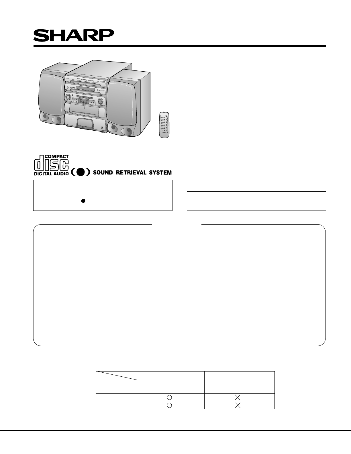
Illustration: CMS-R600X(BK)
CMS-R600X/R600XT
SER VICE MANUAL
No. S8644CMSR600X
CMS-R600X(BK)
CMS-R600XT(BK)
• SRS technology Licensed from SRS Labe. SRS technology holds
the follwing patents: U.S. Patent No. 4,748,669, U.S. Patent No.
4,841,572 and U.S. Patent No. 4,866,774.
• SRS the SRS Logo ( ) and the SOUND RETRIEVAL SYSTEM
are registered trademarks of SRS Labs, Inc.
• In the interests of user-safety the set should be restored to its
original condition and only parts identical to those specified
should be used.
CONTENTS
SPECIFICATIONS ............................................................................................................................................................. 2
VOLTAGE SELECTION..................................................................................................................................................... 2
NAMES OF PARTS ........................................................................................................................................................... 3
OPERATION MANUAL...................................................................................................................................................... 5
DISASSEMBLY.................................................................................................................................................................. 6
REMOVING AND REINSTALLING THE MAIN PARTS..................................................................................................... 8
ADJUSTMENT................................................................................................................................................................. 10
NOTES ON SCHEMATIC DIAGRAM .............................................................................................................................. 12
TYPES OF TRANSISTOR AND LED .............................................................................................................................. 12
BLOCK DIAGRAM ........................................................................................................................................................... 13
SCHEMATIC DIAGRAM / WIRING SIDE OF P.W.BOARD............................................................................................. 16
WAVEFORMS OF CD CIRCUIT...................................................................................................................................... 36
LCD DISPLAY.................................................................................................................................................................. 37
TROUBLESHOOTING (CD SECTION) ........................................................................................................................... 38
FUNCTION TABLE OF IC ............................................................................................................................................... 42
REPLACEMENT PARTS LIST/EXPLODED VIEW
Page
DIFFERENCE BETWEEN CMS-R600X(BK) AND CMS-R600XT(BK)
CMS-R600XT(BK)CMS-R600X(BK)
POWER AC 110/127/220/230-240 V, AC 220 V, 50 Hz
SOURCE 50/60 Hz
SPEAKER
SRS
SHARP CORPORATION
Page 2
CMS-R600X/R600XT
FOR A COMPLETE DESCRIPTION OF THE OPERATION OF THIS UNIT, PLEASE REFER
TO THE OPERATION MANUAL.
SPECIFICATIONS
General
Power source: AC 110/127/220/230-240 V,
(CMS-R600X) 50/60 Hz
Power source: AC 220 V, 50 Hz
(CMS-R600XT)
Power consumption: 170 W
Dimensions: Width; 360 mm (14-3/16")
Height; 390 mm (15-3/8")
Depth; 379 mm (14-15/16")
Weight: 7.3 kg (16.1 lbs.)
Amplifier section
Output power: PMPO; 300 W (total)
MPO; 84 W (42 W + 42 W)
(10 % T.H.D.)
RMS; 50 W (25 W +25 W)
(10 % T.H.D.)
Input terminals: VIDEO/AUX; 245 mV/47 kohms
Output terminals: Speakers; 8 ohms
Headphones; 8 - 50 ohms
(recommended; 32 ohms)
Tuner section
Frequency range: FM; 88 - 108 MHz
AM; 531 - 1,620 kHz
Cassette deck section
Frequency response: 50 - 14,000 Hz (Normal tape)
Motor: DC motor with electronic governor
x 1
Signal/noise ratio: 55 dB (TAPE 1, playback)
50 dB (TAPE 2, recording/
playback)
Wow and flutter: 0.15 % (WRMS)
Bias and erasure system: AC
Tape speed: 4.76 cm/sec. (1-7/8 ips.)
Heads: TAPE-1; Playback x 1
TAPE-2; Record/Playback x 1
Erase x 1
Compact disc player section
Type: 5-disc multi-play compact disc
Signal readout: Non-contact; semiconductor laser
Rotational speed: 200 - 500 rpm CLV, Approx.
Error correction: CIRC (Cross Interleave Reed-
Quantization: 16-bit linear
Filter: 4-times oversampling digital
D/A Converter: 1-bit D/A converter
Frequency response: 20 - 20,000 Hz
Dynamic range: 90 dB (1 kHz)
Wow and flutter: Unmeasurable
player
Solomon Code)
filter
(less than 0.001% W. peak)
Speaker system (CMS-R600X ONLY)
Type: 3-way type
woofer,
tweeter]
Maximum input power: 50 W
Rated power: 25 W
Impedance: 8 ohms
Dimensions: Width; 215 mm (8-1/2")
Height; 390 mm (15-3/8")
Depth; 195 mm (7-11/16")
Weight: 3.4 kg (7.5 lbs.)/each
Specifications for this model are subject to change without
prior notice.
[13 cm (5-1/8")
5 cm (2") tweeter and super
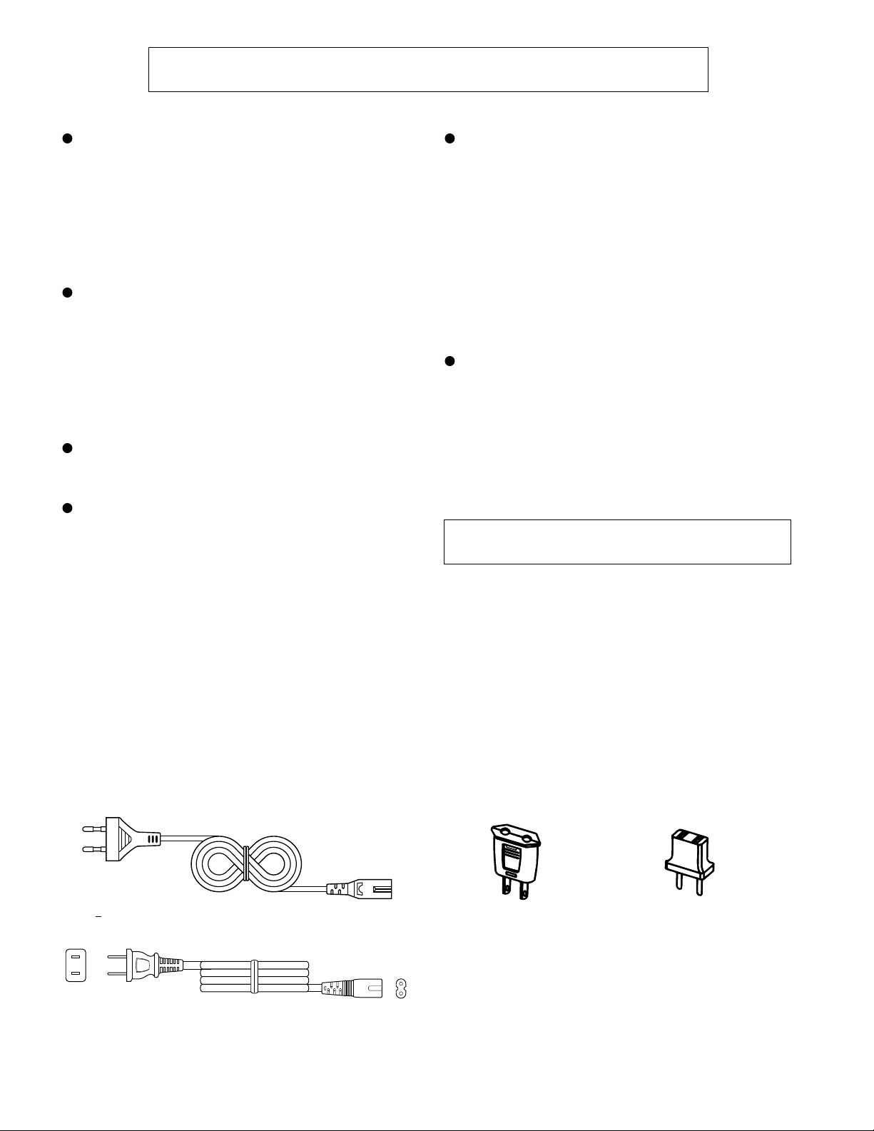
VOLTAGE SELECTION
Before operating the unit on mains, check the preset voltage. If the votage is different from your local voltage. Slide the AC power
supply socket cover by slightly loosing the screw to the visible indication of the side of your local voltage.
QACCE0005AW00 92LPLUG155A 92LPLUG027
92LCoRD577B
Figure 2 AC POWER SUPPLY CORD AND AC PLUG ADAPTOR
– 2 –
Page 3
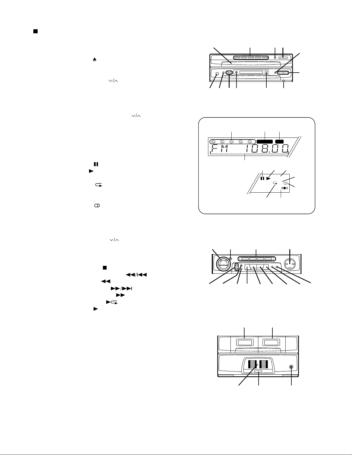
Front panel
1. Disc Tray
2. Disc Number Select Buttons
3. Disc Skip Button
4. Open/Close Button:
5. Power Switch
6. (TUNER) Memory Button
7. Tuning Up/Down Buttons:
8. Timer Indicator
9. Remote Control Sensor
10. Reset Button
11. Band Selector Button
12. Preset and Time Up/Down Buttons:
NAMES OF PARTS
1234
567
CMS-R600X/R600XT
11
12
8910
13. Disc Number Indicator
14. Extra Bass Indicator: X-BASS
15. Record Indicator: REC
16. Function/CD Track/CD Counter/Frequency/
Preset Channel/Volume Indicator
17. CD Pause Indicator:
18. CD Play Indicator:
19. Memory Indicator
20. CD Repeat Indicator:
21. SRS Indicator (CMS-R600X ONLY)
22. FM Stereo Mode Indicator: ST
23. FM Stereo Indicator:
24. Equalizer Mode Buttons
25. Extra Bass Button: X-BASS
26. Function Selector Buttons
27. Volume Up/Down Buttons:
28. Editing Speed Selector Buttons
29. CD Pause Button
30. Record Pause Button
31. (CD/TAPE) Stop Button:
32. (CD) Track Down/Review Button:
(TAPE) Rewind Button:
33. (CD) Track Up/Cue Button:
(TAPE) Fast Forward Button:
34. (CD) Play/Repeat Button:
(TAPE) Play Button:
35. Memory/Set Button
36. Clock/Timer Button
13
5432
16
X-BASS
REC
54321
14
X-BASS
17
kHz
MHz
20
15
REC
18 19
MEMORY
ST
SRS
21
24 25 26 27
28
3029
31 32 33 34
37
38
MEMORY
22
23
35
ST
36
37. (TAPE 1) Cassette Compartment
38. (TAPE 2) Cassette Compartment
39. Level Meters
40. 3D Surround Mode Button (CMS-R600X ONLY)
41. Headphone Socket
– 3 –
39 40
41
(Illustration: CMS-R600X)
Page 4
CMS-R600X/R600XT
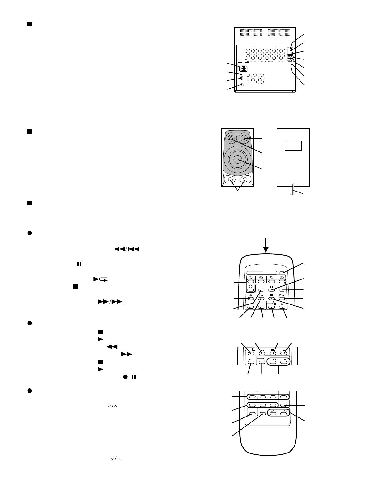
Rear panel
1. Speaker Terminals
2. Phono Power Supply Socket (DC 12V)
(CMS-R600X ONLY)
3. AC Power Input Socket
4. AC Voltage Selector (CMS-R600X ONLY)
5. FM 75 ohns Aerial Terminal
6. Aerial Earth Terminal
7. AM Loop Aerial Socket
8. Phono Input Sockets (CMS-R600X ONLY)
9. Video (Audio Signal) / Auxiliary Input Sockets
10. Phono/Auxiliary/Video Input Selector Switch
(CMS-R600X ONLY)
11. Span Selector Switch (CMS-R600X ONLY)
Speaker Section
12. Tweeter
13. Super Tweeter
14. Woofer
15. Bass Reflex Ducts
16. Speaker Wire
5
6
7
1
2
3
4
8
9
10
11
12
13
14
Remote Control
1. Remote Control Transmitter LED
2. 3D Surround Mode Button (CMS-R600X ONLY)
CD control section
3. Disc Number Select Buttons
4. Track Down/Review Button:
5. Disc Skip Button
6. Pause Button:
7. Random Button
8. Play/Repaet Button:
9. Stop Button:
10. Memory Button
11. Track Up/Cue Button:
12. Clear Button
Tape Control Section
13. (TAPE 1) Stop Button:
14. (TAPE 1) Play Button:
15. (TAPE 2) Rewind Button:
16. (TAPE 2) Fast Forward Button:
17. (TAPE 2) Stop Button:
18. (TAPE 2) Play Button:
19. (TAPE 2) Record Pause Button:
3
4
5
15
11
15
16 17 18
19 20
16
1
2
6
7
8
9
1210
1413
21
Tuner control section
20. Band Selector Button
21. Preset Up/Down Buttons:
22. Function Selector Buttons
23. Balance Control Buttons
24. Power Button
25. Extra Bass Button: X-BASS
26. Equalizer Mode Selector Button
27. Volume Up/Down Buttons:
– 4 –
22
23
24
25
26
27
(Illustration: CMS-R600X)
Page 5
OPERATION MANUAL
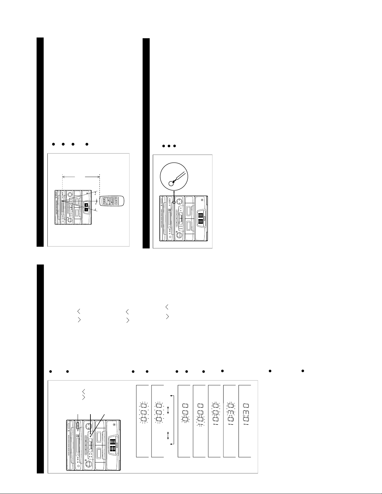
SETTING THE CLOCK
Setting method when the POWER switch is in the STAND-BY
position.1Press the MEMORY/SET button.
When the power is ON, press the CLOCK/TIMER button.
Then, within 5 seconds, press the MEMORY/SET button.
2
Press the PRESET/TIME ( or ) button to select the time
display.
PRESET/
TIME ( )
CLOCK/
TIMER
MEMORY/
SET
1
2
AM 0:00 AM 12:000:00
3
4
5
6
7
"0:00" → The 24- hour display will appear.
(0:00 - 23:59)
"AM 0:00" → The 12-hour display will appear.
(AM 0:00 - PM 11:59)
"AM 12:00" → The 12-hour display will appear.
(AM 12:00 - PM 11:59)
3
Press the MEMORY/SET button.
4
Press the PRESET/TIME ( or ) button to adjust the hour.
Press the PRESET/TIME button once to advance the time by
1 hour. Press for more than 0.5 seconds to advance continu-
ously.
When the 12-hour display is selected, "AM" will change auto-
matically to "PM".
5
Press the MEMORY/SET button.
6
Press the PRESET/TIME ( or ) button to adjust the
minutes.
Press the button for at least 0.5 seconds to advance continu-
ously.
The hour setting will not advance even if minutes advance
from "59" to "00".
7
Press the MEMORY/SET button.
The clock starts operating from "0" seconds. (Seconds are
not displayed.)
Note:
In the event of a power failure or when the AC power lead
is disconnected, the clock display will go out.
When the AC power supply is resumed, the clock display will
flash on and off to indicate that the time must be reset.
If this happens, follow steps 1 and 4 - 7 in the procedure
described above.
To change the clock time:
1
Whilst the clock is displayed, press the MEMORY/SET button.
When the power is ON, press the CLOCK/TIMER button.
Then, within 5 seconds, press the MEMORY/SET button.
2
Perform steps 4 - 7 above.
To see the time display: (When the power is ON)
Press the CLOCK/TIMER button.
The time display will appear for about 5 seconds.
To switch the time display mode:
1
Set the POWER switch to STAND-BY.
2
Whilst holding down the CLOCK/TIMER button, press the
POWER switch twice.
3
Perform steps 1 - 7 above.
In this example, the clock is set for the 24-hour
(0:00) system.
15
15
Notes concerning use:
Replace the batteries if control distance decreases or oper-
ation becomes erratic.
Periodically clean the transmitter LED on the remote control
and the sensor on the main unit with a soft cloth.
Exposing the sensor on the main unit to strong light may in-
terfere with operation. Change the lighting or the direction of
the unit.
Keep the remote control away from moisture, excessive heat,
shock, and vibrations.
0.2 m - 6 m
(8" - 20')
PREPARATION FOR USE
RESETTING THE MICROCOMPUTER
Reset the microcomputer by performing the following
procedure for the cases shown below:
To erase all of the stored memory contents, or
If the display does not function properly, or
The unit does not operate properly.
1
Set the POWER switch to STAND-BY.
2
Disconnect the AC power lead from the AC socket.
3
Press the RESET button for at least 3 seconds.
RESET
CMS-R600X/R600XT
– 5 –
Page 6
CMS-R600X/R600XT
DISASSEMBLY
Caution on Disassembly
Follow the below-mentioned notes when disassembling
the unit and reassembling it, to keep it safe and ensure
excellent performance:
1. Take cassette tape and compact disc out of the unit.
2. Be sure to remove the power supply plug from the wall
outlet before starting to disassemble the unit.
3. Take off nylon bands or wire holders where they need be
removed when disassembling the unit. After servicing
the unit, be sure to rearrange the leads where they were
before disassembling.
4. Take suffcient care on static electricity of integrated
circuits and other circuits when servicing.
(A1) x 2
ø3 x 12mm
Side Panel
(B1) x 2
ø3 x 10mm
Top Cabinet
(A1) x 2
ø3 x 12mm
Side Panel
MAIN UNIT
STEP REMOVAL FIGURE
1 Top Cabinet 1. Screw .....................(A1) x4 6-1
2 Side Panel 1. Screw .....................(B1) x6 6-1
(Left/Right)
3 CD Player Unit/ 1. Turn on the power supply,.
CD Tray Cover open the disc tray, take out
4 Back Board 1. Screw .................... (D1) x8 6-2
5 Front Panel 1. Screw ..................... (E1) x3 6-3
6 Main PWB/ 1. Screw ..................... (F1) x3 6-3
SRS PWB 2. Socket .................... (F2) x1
7 Power PWB 1. Screw .................... (G1) x5 6-3
8 Tape Mechanism 1. Open the cassette holder.
9 Switch PWB 1. Screw ..................... (J1) x4 7-1
10 Display PWB 1. Screw .....................(K1) x9 7-1
11
Headphones PWB
12 Level Meter PWB 1. Screw ................... (M1) x2 7-2
13 Switch PWB 1. Screw .................... (P1) x2 7-2
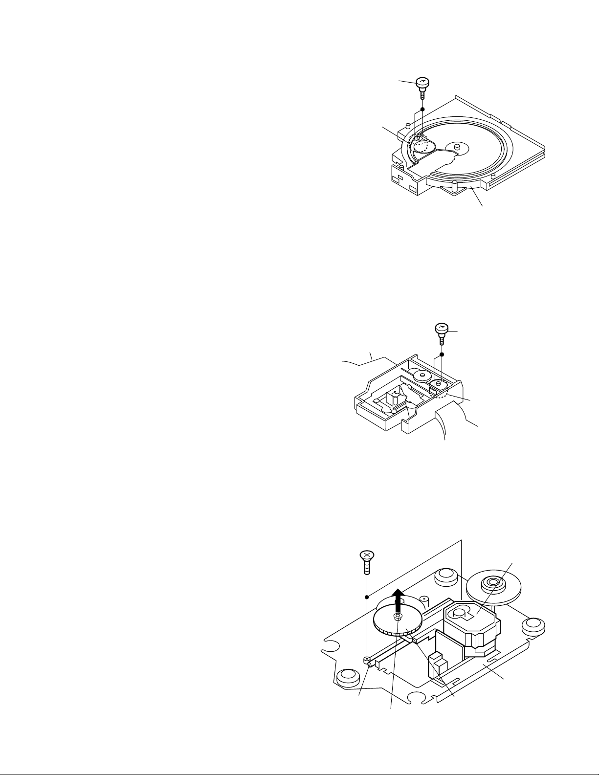
14 Turntable 1. Screw .................... (Q1) x2 7-3
15 CD Tray 1. Screw .................... (R1) x4 7-3
16 CD Servo PWB 1. Screw .....................(S1) x2 7-4
17 Sensor PWB 1. Screw ..................... (T1) x1 7-4
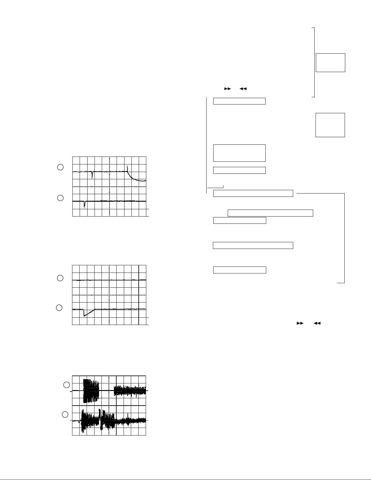
18 CD Mechanism 1. Screw .................... (U1) x2 7-5
the CD cover, and close.
(Note 1)
2. Hook ...................... (C1) x2 6-2
3. Screw .................... (C2) x5
4. Flat Wire .................(C3) x1
5. Socket ................... (C4) x2 6-3
2. Socket ....................(E2) x4
3. Flat Cable.............. (E3) x3
3. Flat Wire ................. (F3) x1
2. Flat Wire .................(H1) x1 7-1
3. Screw .................... (H2) x6
1. Screw ..................... (L1) x1 7-1
2. Cover..................... (Q2) x1
2. Guide..................... (R2) x2
2. Hook ....................... (T2) x2
Note 1: If the power supply cannot be turned on, <A> turn the
pulley by hand as shown in Figure 6-2 to open the disc
tray.
PROCEDURE
SPEAKER BOX [CMS-R600X ONLY]
STEP REMOVAL PROCEDURE FIGURE
1 Speaker 1. Front Panel ............. (A1) x1 7-6
2. Screw ...................... (A2) x4 7-7
3. Screw ...................... (A3) x2
Pulley
CD Player Unit
(D1) x 3
ø3 x 8mm
(C2) x 3
ø3 x 12mm
(D1) x 2
ø3 x 8mm
Power PWB
(C4) x 1
<A>
(G1) x 4
ø4 x 6mm
(E3) x 3
(B1) x 2
ø3 x 12mm
(C2) x 1
ø3 x 10mm
(C4) x 1
(F1) x 1
ø3 x 10mm
Figure 6-1
(D1) x 3
ø3 x 12mm
Figure 6-2
(G1) x 1
ø3 x 10mm
Front Panel
Main PWB
(C1) x 1
(E2) x 2
SRS
PWB
(E1) x 3
ø3 x 10mm
(B1) x 2
ø3 x 10mm
CD Tray Cover
(C1) x 1
(C2) x 1
ø3 x 10mm
(C3) x 1
(F2) x 1
(E2) x 2
(F1) x 2
ø3 x 10mm
(F3) x 1
– 6 –
Figure 6-3
Page 7
CMS-R600X/R600XT
(J1) x 4
ø3 x 10mm
(K1) x 9
ø3 x 10mm
(L1) x 1
ø3 x 8mm
Headphones PWB
Front Panel
Switch PWB
(H2) x 6
ø3 x 10mm
Figure 7-1
Display PWB
(H1) x 1
Tape
Mechanism
(S1) x 2
ø3 x 10mm
CD Servo
PWB
CD Tray
CD Mechanism
(T1) x 1
ø3 x 10mm
Sensor PWB
(T2) x 2
Figure 7-4
(U1) x 2
Special
Level Meter PWB
(M1) x 2
ø3 x 10mm
CD Tray
(R2) x 1
(P1) x 1
ø3 x 10mm
(Q1) x 2
ø3 x 10mm
Turntable
(P1) x 1
ø3 x 10mm
Figure 7-2
Switch PWB
(Q2) x 1
Screw Driver
(A2) x 4
ø
4 x 32mm
Figure 7-5
Front Panel
(A1) x 1
Figure 7-6
(A3) x 2
ø
4 x 32mm
(R1) x 2
ø3 x 10mm
(R2) x 1
Figure 7-3
Loading
Chassis
(R1) x 2
ø3 x 10mm
Figure 7-7
– 7 –
Page 8
CMS-R600X/R600XT
REMOVING AND REINSTALLING THE MAIN PARTS
TAPE MECHANISM SECTION
Perform steps 1, 2, 3, 4, 5 and 8 of the disassembly method to
remove the tape mechanism.
How to remove the record/playback and erase
heads (TAPE 2) (See Fig. 8-1.)
1. Carefully bend the record/playback head pawls (A1) x 2
pcs., in the direction of the arrow <A> , and remove the
record/playback head upwards.
2. Carefully bend the three pawls (B1) x 3 pcs., in the arrow
direction <B>, and remove the erase head upward.
How to remove the playback head (TAPE 1)
(See Fig. 8-2.)
1. Carefully bend the playback head pawls (C1) x 2 pcs., in the
direction of the arrow <C>, and remove the playback head
upwards.
How to remove the pinch roller (TAPE 1/2)
(See Fig. 8-3.)
1. Carefully bend the pinch roller pawl in the direction of the
arrow <D>, and remove the pinch roller (D1) upwards.
Note:
When installing the pinch roller, pay attention to the spring
mounting method.
TAPE 2
Erase Head
<B>
<A>
<B>
Pawl (B1) x3
Playback Head
Figure 8-1
TAPE 1
<C>
Record/Playback
Head
<A>
<B>
Pawl (A1) x2
<C>
How to remove the belt (TAPE 1) (See Fig. 8-4.)
1. Remove the main belt (E1) x 1 pc., from the motor side.
How to remove the belt (TAPE 2) (See Fig. 8-4.)
1. Remove the tape 1 main belt (E1) x 1pc., from the motor
side.
2. Remove the tape 2 main belt (F1) x 1pc., from the motor
side.
3. Remove the FF/REW belt (F2) x 1 pc.
How to remove the motor
(See Figs. 8-4 and 8-5.)
1. Remove the belt.
2. Remove the screws (G1) x 2 pcs., to remove the motor
fixture.
3. Remove the screws (G2) x 2 pcs., to remove the motor.
Note:
When mounting the motor, pay attention to the motor mounting
angle.
(G1) x2
ø2 x4mm
Motor
FF/REW Belt
(F2) x1
TAPE 2
Flywheel
Pawl (C1) x2
Figure 8-2
Pinch Roller (D1) x1
Figure 8-3
Motor
Main Belt
(F1) x1
<D>
Pawl
TAPE 1
Flywheel
Main Belt
(E1) x1
(G2) x2
ø2 x4mm
Figure 8-5
Motor Bracket
– 8 –
TAPE 2
Main Belt
(F1) x1
Motor
TAPE 1
Main Belt
(E1) x1
Figure 8-4
Page 9
( C1 ) x2
ø2.6 x6mm
( C2 ) x1
( C3 ) x1
( C4 ) x1
CD Mechanism
Pickup
CD MECHANISM SECTION
Perform steps 1, 2, 3, 14, 15 and 16 of the disassembly
method to remove the CD mechanism.
How to remove the loading motor
(See Fig. 9-1)
1. Remove the screws (A1) x 2 pcs., to remove the loading
motor.
CMS-R600X/R600XT
( A1 ) x2
ø2.6 x5mm
Loading Motor
CD Tray
Figure 9-1
How to remove the turntable up/down motor
(See Fig. 9-2)
1. Remove the screws (B1) x 2 pcs., to remove the turntable
up/down motor.
How to remove the pickup (See Fig. 9-3)
1. Remove the screws (C1) x 2 pcs., to remove the shaft (C2).
2. Remove the stop washer (C3) x 1 pc., to remove the gear
(C4).
3. Remove the pickup.
CD Tray
( B1 ) x2
ø2.6 x5mm
Turntable
Up/Down Motor
Figure 9-2
Figure 9-3
– 9 –
Page 10
CMS-R600X/R600XT
ADJUSTMENT
TAPE MECHANISM SECTION
• Driving Force Check
Torque Meter Specified Value
Play: TW-2412 Tape 1: Over 50 g
Tape 2: Over 100 g
• Torque Check
Torque Meter
Play: TW-2111 30 to 60 g. cm 30 to 60 g.cm
Fast forward: TW-2231 — 80 to 135 g.cm
Rewind: TW-2231 — 80 to 135 g.cm
• Tape Speed
Test Tape
Normal MTT-111 VRM1 3,000 ± Speaker
speed 30 Hz terminal
Adjusting
TUNER SECTION
fL: Low-range frequency
fH: High-renge frequency
• AM IF/RF
Signal generator: 400 Hz, 30%, AM modulated
Test Stage
IF 450 kHz 1,720 kHz T351 *1
Band — 530 kHz (fL): T333 *2
Coverage 3.4 V ± 0.1 V
Tracking 990 kHz 990 kHz (fL): T331 *1
*1. Input: Antenna, Output: TP302
*2. Input: Antenna, Output: TP301
Frequency Frequency
Display
Tape 1
Point
Specified Value
Specified
Value
Setting/
Adjusting
Parts
Tape 2
Instrument
Connection
(Load
resistance:
8 ohms)
Instrument
Connection
• FM RF
Signal generator: 1 kHz, 75 kHz dev., FM modulated
Test Stage Instrument
Band — 87.50 MHz L303(fL): *1
Coverage 1.85 V ± 50 mV
RF 98.00 MHz 98.00 MHz L302 *2
Frequency
(10-30 dB)
Frequency
Display
Serring/
Adjusting
Point
Connection
*1. Input: Antenna, Output: TP301
*2. Input: Antenna, Output: Speaker terminal
• Detection
Signal generator: 10.7 MHz, FM sweep generator
Test
Stage
IF 10.7 MHz 98.00 MHz T301(Turn Input: Pin 1 of
Frequency
Frequency
Display
Adjusting
Parts
the core of IC301
transformer Output: TP302
T301 fully
counterclookwise.)
Instrument
Connection
• FM Mute Level
Frequency
98.00 MHz 98.00 MHz VR351 *1 Input: SO301
(25 dBµV) Output: Speaker
Frequency
Display
Adjusting
Parts
Instrument
Connection
Terminal
*1 Adjust so that an output signal appears.
TAPE
SPEED
VRM1
TAPE MECHANISM PWB-G
C364
R358
12
TP302
MAIN PWB-A1
AM IF
T351
VR351
IC351
1
24
2113
FM BAND
COVERAGE fL
L303
FM MUTE
LEVEL
T301
FM IF
TP301
AM BAND
COVERAGE fL
T333
AM TRAKING fL
Figure 10 ADJUSTMENT POINTS
– 10 –
IC301
T331
1
L302
FM RF
SO301
ANTENNA
TERMINAL
2
AM LOOP ANTENNA
1
CNP301
Page 11
CMS-R600X/R600XT
CD SECTION
Since this CD system incorporates the following automatic
adjustment function, when the pickup is replaced, it is not
necessary to readjust it.
Since this CD unit does not need adjustment, the combination
of PWB and laser pickup unit is not restricted.
• Automatic adjustment item
1. Focus offset (Fig. 11-1)
2. Tracking offset (Fig. 11-2)
3. E/F balance (tracking error balance) (Fig. 11-3)
4. RF level AGC function (HF level: constant)
5. RF level automatic follow-up of the tracking gain
This automatic adjustment is performed each time a disc is
changed. Therefore, each disc is played back using the
optimal settings.
0.1s
0.50 V
IC1 20 FE
FOCUS
OFF-SET
0.1s
0.50 V
IC1 7 TE
10ms
0.50 V
IC1 20 FE
Figure 11-1
ADJUST
TRACKING
OFF-SET
ADJUST
1
2
Enlarged
View
CD TEST MODE
When the CD, STOP and POWER keys are
pressed at the same time, to turn on the power,
the unit will enter the test mode.
↓
"VOL" will appear. After "CD" has appeared, all
of the LCDs will light up.
↓
The OPEN/CLOSE operation can be performed
manually.
↓ It is OK if the display does not change.
Use of the
pickup.
→ Press the PLAY key.
←
→ Press the APMS MEMORY key. ←
or key allows you to slide the
↓ All of the LCDs will go out.
A TOC and IL will be performed and normal playback can be performed. When
the following keys are pressed during
playback, the track numbers can be specified directly.
↓
DISC 1 → Track 3
DISC 2 → Track 8
DISC 3 → Track 15
↓
Press the STOP key.
↓
Stop
↓ All of the LCDs will go out.
The tracking servo will turn on, and playback will begin.
↓ The track No. and time will appear.
Press the STOP key.
↓ "01 0:00" will appear.
The pickup will return normally to the STOP position.
↓
Press the APMS MEMORY key.
↓ "01 0:00" will appear.
The tracking servo will turn off, and playback will begin.
↓
Press the STOP key.
↓ "01 0:00" will appear.
The pickup will return normally to the STOP position.
Initialization
(IL) is not
performed.
The display
will look the
same as
usual.
10ms
0.50 V
IC1 7 TE
200 ms
1V/diV
IC 1 15
TO
200 ms
1V/diV
IC 1 7
TE
Figure 11-2
Figure 11-3
TRACKING
OFF-SET
ADJUST
1
2
TRACKING/
ERROR
BARANCE
ADJUST
1
2
Cancel method: POWER OFF
LCD display: After the PLA Y or APMS MEMORY key has been
pressed, the track No. and time only will appear
(valid). The other items are optional.
Note: The pickup can be slid using the
or key only
while in the stop mode.
INITIALIZING THE CD CHANGER MECHANISM
When the CD, DOWN and POWER keys are pressed at the
same time to turn on the power, the CD changer mechanism
will be initialized.
• The entire CD APMS memory will be cleared.
• The FUNCTION button can be used to start the CD. The
other initializations are the same as usual.
• The CD changer mechanism will be initialized. DISC 1 will be
chucked, initialized, and stopped.
• "INITIAL" will flash on the LCD. After initialization, the LCD
will return from the display of DISC 1 being initialized to the
normal display.
ALL CLEAR AND RE-START FUNCTION
When the CLEAR and POWER keys are pressed to turn on
the power, the entire internal memory will be cleared and the
mechanism will run from address 0.
All of the tuner presets, APMS, TOC and disc numbers which
were last stored in memory will be cleared, and the tuner,
changer mechanism and all of the other items will be initialized.
– 11 –
Page 12
CMS-R600X/R600XT
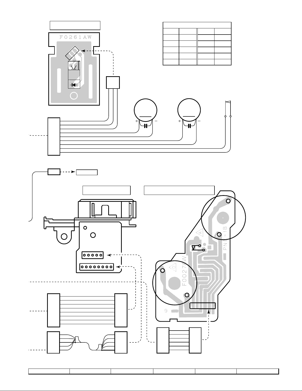
NOTES ON SCHEMATIC DIAGRAM
• Resistor:
To differentiate the units of resistors, the symbol as K and M
are used: the symbol K means 1000 ohm and the symbol M
means 1000 kohm and the resistor without any symbol is an
ohm resistor. The resistor designated “Fusible” is a fuse type
resistor.
• Capacitor:
To indicate the unit of capacitor, a symbol P is used: this
symbol P means Pico-farad and the unit of the capacitor
without such a symbol is microfarad. As to electrolytic
capacitor, the expression “capacitance/withstand voltage”
is used.
(CH), (TH), (RH), (UJ): Temperature compensation
(ML): Mylar type
(P.P.): Polypropylene type
• Schematic diagram and Wiring Side of P.W.Board for this
model are subject to change for improvement without prior
notice.
REF. NO DESCRIPTION POSITION POSITIONREF. NO DESCRIPTION
SW2 DISC UP ON—OFF
SW4 PICKUP IN ON—OFF
SW291 SPAN SELECTOR 100/10—
[CMS-R600X ONLY] 50/9
SW421 PHONO/VIDEO/AUX PHONO—
[CMS-R600X ONLY] VIDEO/AUX.
SW561 3D SURROUND ON—OFF
SW702 CD DISC1 ON—OFF
SW703 CD DISC2 ON—OFF
SW704 CD DISC3 ON—OFF
SW705 CD DISC4 ON—OFF
SW706 CD DISC5 ON—OFF
SW707 CD DISC SKIP ON—OFF
SW708 CD OPEN/CLOSE ON—OFF
SW709 FLAT ON—OFF
SW710 BGM ON—OFF
SW711 VOCAL ON—OFF
SW712 HEAVY ON—OFF
SW713 X-BASS ON—OFF
SW714 TUNING UP ON—OFF
SW715 MEMORY ON—OFF
SW716 POWER ON—OFF
SW717 FORWARD ON—OFF
SW718 PRESET UP/TIME UP ON—OFF
SW719 STOP ON—OFF
• The indicated voltage in each section is the one measured
by Digital Multimeter between such a section and the chassis with no signal given.
1. In the tuner section,
( ) indicates AM
< > indicates FM stereo
2. In the main section, a tape is being played back.
3. In the deck section, a tape is being played back.
( ) indicates the record state.
4. In the power section, a tape is being played back.
5. In the CD section, the CD is stopped.
• Parts marked with “
” ( ) are important for
maintaining the safety of the set. Be sure to replace these
parts with specified ones for maintaining the safety and
performance of the set.
SW720 REC PAUSE ON—OFF
SW721 CD PAUSE ON—OFF
SW722 TUNING DOWN ON—OFF
SW723 EDIT HIGH ON—OFF
SW724 EDIT NORMAL ON—OFF
SW725 REWIND ON—OFF
SW726 PRESET DOWN/TIME DOWN ON—OFF
SW728 VOLUME UP ON—OFF
SW729 CLEAR/TIMER ON—OFF
SW730 MEMORY/SET ON—OFF
SW732 PLAY/REPEAT ON—OFF
SW734 BAND ON—OFF
SW735 VOLUME DOWN ON—OFF
SW736 VIDEO/AUX ON—OFF
SW737 TAPE1 2 ON—OFF
SW738 TUNER ON—OFF
SW739 CD ON—OFF
SW740 RESET ON—OFF
SW801 OPEN/CLOSE ON—OFF
SW901 VOLTAGE SELECTOR 110—127—
[CMS-R600X ONLY] 220—230-240
SWM3 FULL PROOF ON—OFF
SWM4 F.A.S. ON—OFF
SWM5 CAM ON—OFF
FRONT
VIEW
ECB
(S) (G) (D)
(1) (2) (3)
2SD468 C
2SK246 GR
KRC102 M
KRC104 M
KTA1266 GR
KTA1270 Y
KTA1271 Y
KTC3194 Y
KTC3199 GR
KTC3200 GR
KTC3203 Y
KTD2058 Y
FRONT VIEW FRONT VIEW
FRONT
KV1236Z23
KDV147C
Figure 12 TYPES OF TRANSISTOR AND LED
– 12 –
VIEW
5N4GTN52
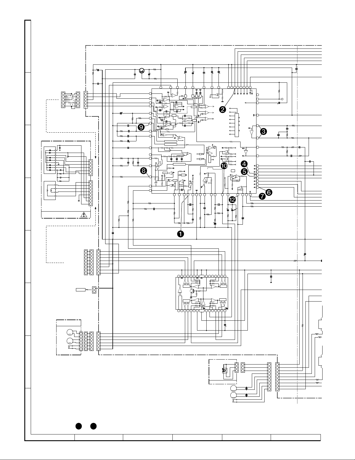
Page 13
IC1
LA9240M
SERVO AMP.
IC2
LC78622E
SERVO/SIGNAL
CONTROL
CLK
DEF/THLD
SLI
SLC
CV+
JP–
JP–
CLV+
EFMIN
EFMO
DEFI
50
49
~
444340
32
20
1
61
9
~
12
10
XVDD
TEST2
VDD
VVDD
+B
43
11
23
6
58
53
SQOUT. RWC. WRQ
RES. CQCK. COIN
~
RVDD
LVDD
RCHO
RVSS
LVSS
LCHO
CONT5
CONT1
DRF
CL
DRF
SL+
SL–
SLD
SPD
FD
TO
FEFIN1
FIN2
LDD
VCC1
CNS10
+5.6V
ASP
+5V
DSP
+5V
ALPC
CONTROL
POWER
LASER
IC51, IC52 : MOTOR DRIVER
2
6
6
2
DISC UP SW
PH2
DISC NO.
SENSOR
5.7V CDSVO
25
19
10
3
51
SECTION
TO MAIN
(OPEN)
L-CH OUT
AUDIO GND
R-CH OUT
GND
12V MECHA
CO IN
SQ OUT
CQCK
LOADING H/L
SLM–
SLM+
RWC
RES
WRC
DRF
DISC NO. SENSOR
PU-IN SW
DISC UP SW
20
19
18
17
16
14
15
13
12
11
10
9
8
7
654
321
Q81
CHANGER MECHA
M2
TURNTABLE
UP/DOWN
LOADING
M1
MOTOR
SW2
REGULATOR
M
M
Q51
7
3
891
TA7291S
IC51
Q52
IC52
TA7291S
7
3
8
9
1
AUDIO
+5V
40
39
38
37
36
41
28
24
~
DEF, CLK, CL, DAT, CE, DRF
44
45
27
16
15
29
~
54
+5.6V
28
13
8
7
21
BA5920FP
M3
SPIN MOTOR
M4
SLIDE MOTOR
Q1
62
PICKUP IN
SW4
TRACKING/
SPIN/SLIDE/
DRIVER
FOCUS/
XL1
16.93MHz
PICKUP UNIT
M
M
TRACKING COIL
FOCUS COIL
+5V
XOUT
XIN
SL+. SL–. DRF
IC5
22
64
27
26
18
17
12
11
2
1
4
321
543130
CMS-R600X/R600XT
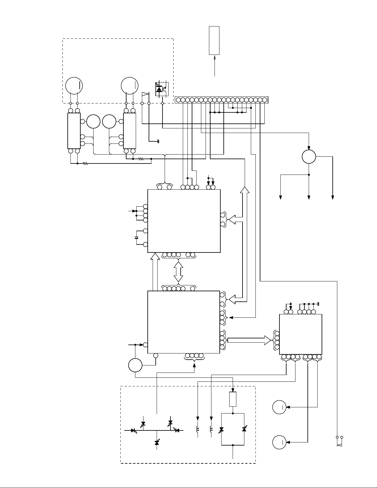
Figure 13 BLOCK DIAGRAM (1/3)
– 13 –
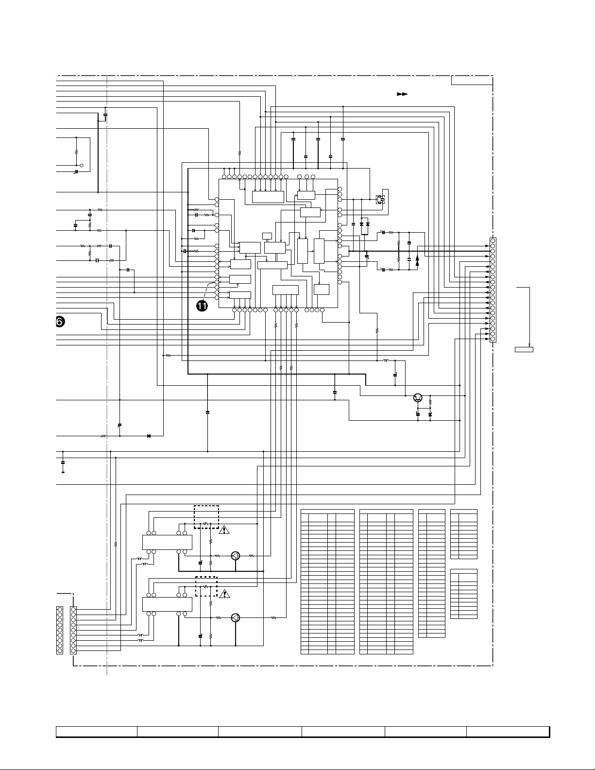
Page 14
CMS-R600X/R600XT
L
S
B
L
SO301
ANTENNA
TERMINAL
FM 75ohms
GND
AM LOOP
ANTENNA
AM ANT.
TERMINAL
PHONO/VIDEO/AUX
FROM CD SECTION
2
1
CNP301
SO401
SW801
CD CHANGER
MM1
TAPE
MOTOR
SWM3
FULL PROOF
SWM4
F.A.S
SOLM1
SOLENOID
SWM5
CAM
L-CH
R-CH
M
1
PHM1
FM RF
FM FRONT END
4
3
L302
AM
ANT.
+B6
TAPE
SPEED
VRM1
IC301
TA7358AP
5
T333T331
FM IF
AM
OSC.
6
T301
MOTOR
DRIVER
+B4
DRIVER
FM IF
FM +B
RF AMP.
CF302
FM MUTE
LEVEL
VR351
9
8
7
FM
L303
OSC.
Q302
SWITCHING
Q712Q711
Q708Q707
Q714Q713
SWITCHING
+B5
AM IF
T351
AM MIX
OUT
1
FM IF DET. /FM MPX. /AM IF
24
21
23
6
AM +B
AM OSC
AM RF IN
X381
4.5MHz
VT
20
1
9
7
FM
Q381
SWITCHING
SOLENOID PLUNGER
CF352 +B5
CF351
AM IF
IN
42
FM DET
IC351
LA1832
16
18
17
DET OUT
MPX IN
AM IN
FM IN
15
22
IC381
LC72131
PLL
3
CE
+B5
TAPE MOTOR
TAPE2 RUN PULSE
TAPE2 FULL PROOF
TAPE1 RUN PULSE
TAPE MECHA STOP
HIGH SPEED
8
X351
11
7
ST
4
DI
VCC
9
13
STEREO
ST
1016
5
CL
FM/AM
12
L OUT
R OUT
MONO/ST
13
8
VDD
21
6
DO
+
L
14
R
15
D351
CD
TUNER
TAPE
CEDICL
252423
L
21
28
R
L
19
30
R
L
17
32
R
16
Q371
Q372
MUTING
17
+B5
IL
40
9
33
3514
RL
RL
TAPE1
P. B. HEAD
L-CH
R-CH
TAPE2
REC/P. B.
HEAD
L-CH
R-CH
ERASE
HEAD
Q201
Q202
SWITCHING
Q203
~
Q206
PBREC
POP
REDUCE
R REC
SWITCHING
T1 L
T1 R
T2 L
T2 R
L NF
R NF
SWITCHING
Q207
Q208
Q272
Q281
L282
REC. /P. B. AMP.
IC201
AN7345K
1
P. B
24
2
23
3
22
6
RECL REC
9
16
12
15
NOR/
CrO
2
Q255
Q256
PB MUTE
Q211
Q212
REC MUTING
Q209
Q210
Q213
VCC
+B5
13
L OUT
4
L
21
R
R OUT
T1/T2
19
L REC IN
7
18
R REC IN
8
17
ALC
11
10
ALC CUT
SWITCHING
Q274
SWITCHING
Q273
Q282 Q283
SWITCHINGSWITCHINGBIAS OSC
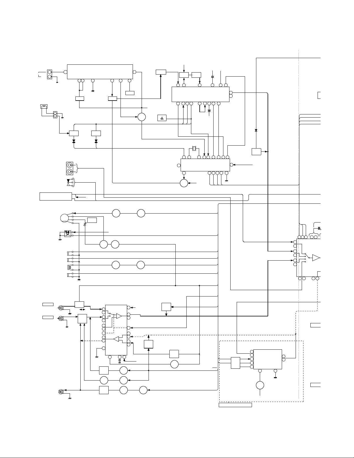
Figure 14 BLOCK DIAGRAM (2/3)
– 14 –
T1/T2
P. B. MUTE
REC
REC BIAS
Q502
Q504
Q506
SRS MODE
SELECTOR
MODE
C-IN
C-OUT
SRS1
PASS
PASS/STEREO/MONO
CMS-R600X ONLY
18
L
R
17
26
24
25
IC501
SRS5250S
SRS
1
VOLTAGE
Q501
REGULATOR
+B5
TO CD
28
R
L
27
15
TO CD
Page 15
T500mA L 250V
F601, F602
L 250V
T2.5A
F902
T3.15A
L 250V
L 250V
T1.6A
F903
L 250V
T3.15A
F901
SWITCHING
SW901
VOLTAGE
SELECTOR
50/60Hz
230 – 240V
600X: AC 110/127/220/
SUPPLY CORD
AC SOCKET
SO901
230 – 240V
110V
127V
220V
600XT
ONLY
T. F
L
R
RL
DC 12V
ONLY
J901
DC SOCKET
FOR RP-R600
Q931 Q930
Q641
+B3
RESET IN
SYSTEM STOP
4.19MHz
XL701
+B3 (5V BACK UP)
+B2
RL
LCD BIAS
~~
COM 0 ~
COM 3
S0 ~ S31
HIGH SPEED
RL
TO CD SECTION
Q926
Q923
+B6(+5.7V)
+5V
Q705
T901
TRANSFORMER
POWER
VCC
+27V
–27V
D901 ~ D904
+5.7V
D702
D705
D704
IC701
OPEN SW
CLOSE SW
DISC UP
PU IN
DISC NO
OUT
AC POWER
D905 ~ D908
P-CONT
SO601
J601
GND
GND
POWER AMP.
LM1876TF
IC601
R-IN
L-IN
R-OUT
L-OUT
SPEAKER SWITCH
HEADPHONES
TERMINAL
SPEAKER
NF
PRE
Q483
Q482
Q481
LMP561
EDGE LAMP
LMP802
32.768kHz
XL702
LMP801
SWITCHING
+B4
BACK LAMP
+B5
L
R
IC431
Q927
Q925
Q924
SW734 ~ SW739
SW732
SW728 ~ SW730
SW702 ~ SW726
Q701 ~ Q704
LED701 ~ LED704
RX701
DETECTOR
POWER FAIL
SW740
Q706
Q710
Q709
F921
LC75394E
DO
DI
CE
CL
DISPLAY
LCD701
TUNER MUTE
+B1
UN SWITCH
RESET
CD
R
L
R
L
R
L
TAPE
TUNER
AUDIO PROCESSOR
TO CD SECTION
SENSOR
REMOTE CONTROL
+B2
REMOTE IN
REGULATOR
VOLTAGE
REGULATOR
VOLTAGE
(ANALOG)+12V
+B5
(MECHA)+12V
+B4
REGULATOR
VOLTAGE
(MICOM)
+B1
REGULATOR
VOLTAGE
ILLUNIMATION GUIDE
LED DRIVER
CEDICL
+B2
KEY
BACK UPRESET
MEMORY
+B2
VDD
GRAPHIC EQUALIZER
VOLUME
GRAPHIC EQUALIZER
X- BASS
36
5
15
27
28
15
4
2
47
46
45
4443
14
11
9
6
12
7
13
8
10
5
1
3
4
1
21
3
PASS
SRS1
COIN
SQOUT
PLAYBACK MUTE
POWER CONT.
TAPE 2 RUN PULSE
TAPE2 FULL PROOF
TAPE 1 RUN PULSE
CQCK
DRF
LODING MOTOR L/H
SLIDE MOTOR–
SLIDE MOTOR +
RWC
RES
WRC
SOLENOID PLUNGER
T1/T2
TAPE REC
TAPE BIAS
TAPE MOTOR
TAPE MECHA STOP
X IN
X OUT
RESET
VDD
VSS
AVSS
VREF
~~
~~~
INITIAL2
INITIAL1
IX0153AWZZ
IC701
SYSTEM
MICROCOMPUTOR
COM OUT
KEY IN
49
48
4
3
41
39
384225
24
23
35
16
15962120
19
18
97
17
5
26
36
37
9
27
40
12
8
7
13
22
98
34
33
2
99
1
32
28
95
92
14
50
58
55
54
51
91
10
11
60
252423
48
1
47
2
46
3
45
4
44
5
43
6
42
7
41
8
40
9
A VSS
VSS
R VREF
L VREF
V REF
36
13
33
16
3514
58
55
21
28
17
32
19
30
57
26
27
391037 3811
12
50
63
56
600X
ONLY
600XT: AC 220 V, 50 Hz
CMS-R600X/R600XT
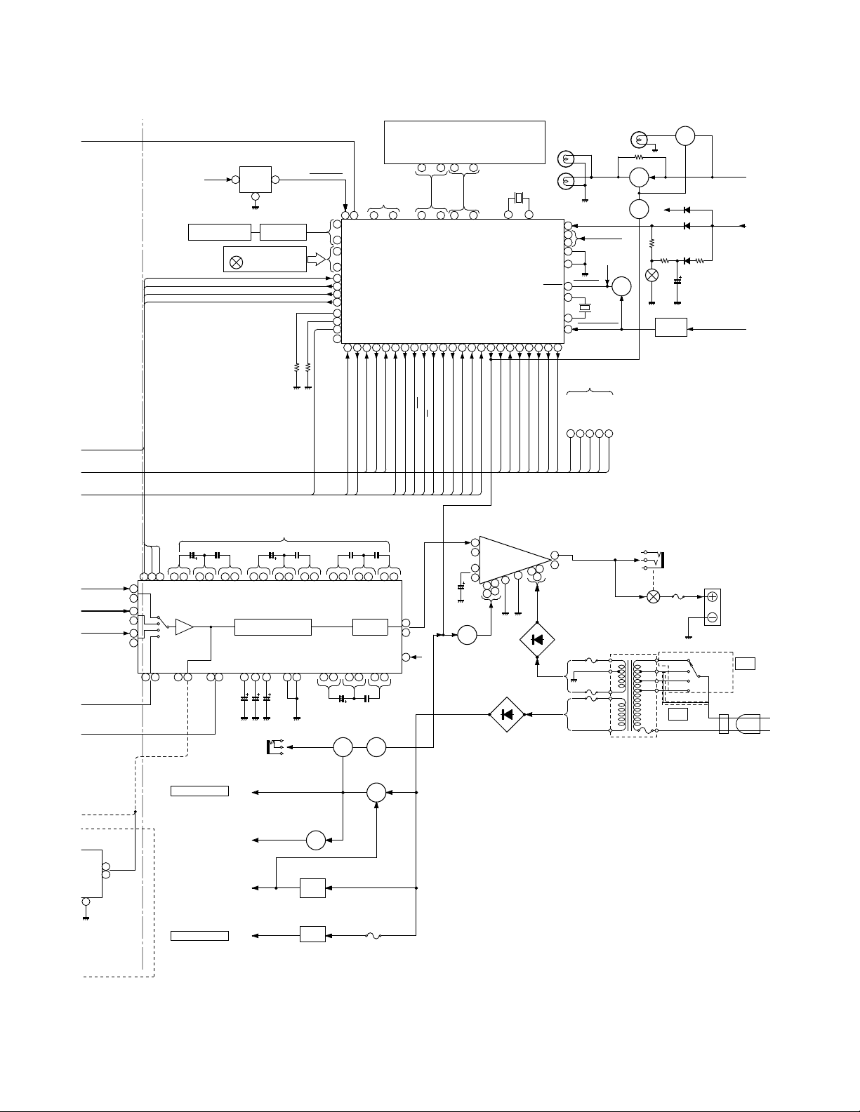
Figure 15 BLOCK DIAGRAM (3/3)
– 15 –
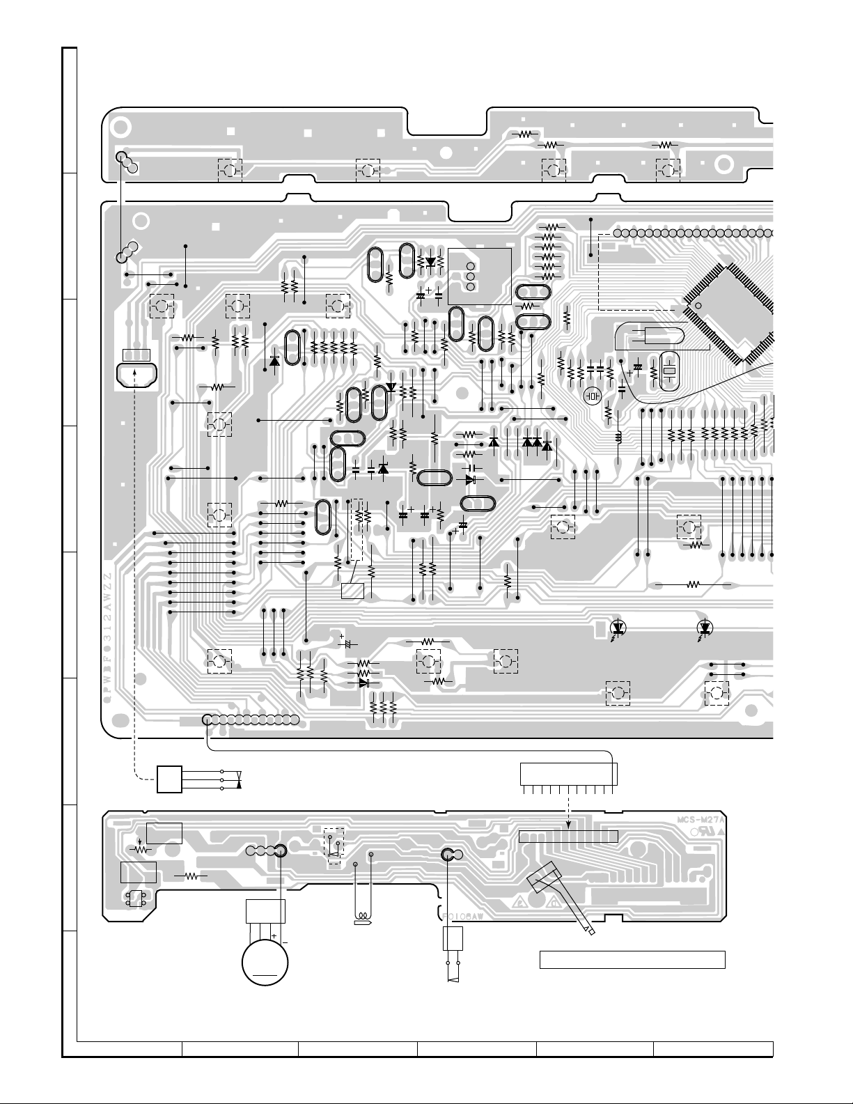
Page 16
CMS-R600X/R600XT
A
CD PWB-C1
P21 9 - H
TO DISPLAY PWB
FC700
R58
R34
48
R33
R41
R62
C45
45
40
20
R28
C49
R14
R60
C22
35
25
R17
C12
Q1
R59
C91
64
1
R32
C62
C31
30
R16
C24
ECB
5
33
32
R15
60
C29
C14
R27
R26
C20
C16
R21
R20
C15
R19
C56
CNP10
135791113151719
2468101214161820
C54
49
50
55
IC2
10
15
16
R89
D2
C11
XL1
48
45
40
33
35
32
30
25
20
17
R22
R39
R29
R94
R88
R23
R40
R87
R86
R49
C92
R43
C17
C55
C63
D8
L1
1
2
3
4
5
6
R100
7
8
9
IC52
1
7
8
14 15
C51
C60
R82
C67
R92
IC5
C25
R98
C48
R25
R24
C68
C52
C21
C19
C18
C70
R76
Q52
L52
28
22
ECB
C81
123
R96
L53
R10
21
D7
R75
R74
C43
C61
C69
R73
R81
ZD81
CNP3
Q81
1
2
3
4
5
6
7
8
1
2
3
4
5
6
LNGR
CNP4
R99
1
C10
R8
R11
R97
C34
C39
5
R9
C8
C9
R7
C42
R36
C33
R35
C32
60
C41
R37
R42
89
7
6
5
4
3
2
1
49
55
10
16 17
IC51
R57
R56
R38
50
IC1
15
R13
C13
R12
L54
R95
Q51
CNP80
1
2
3
4
5
6
7
8
9
L51
R91
123
R93
C57
C50
B
C
5
4
D
3
11
2
E
9
F
C35
C37
CNP2
C3
1
2
3
4
5
C38
C40
C5
C6
C7
C2
C1
C4
R1
R3
R2
R4
R5
R6
64
G
8
1 6 7
H
• The numbers 1 to 12 are waveform numbers shown in page 36.
1
23456
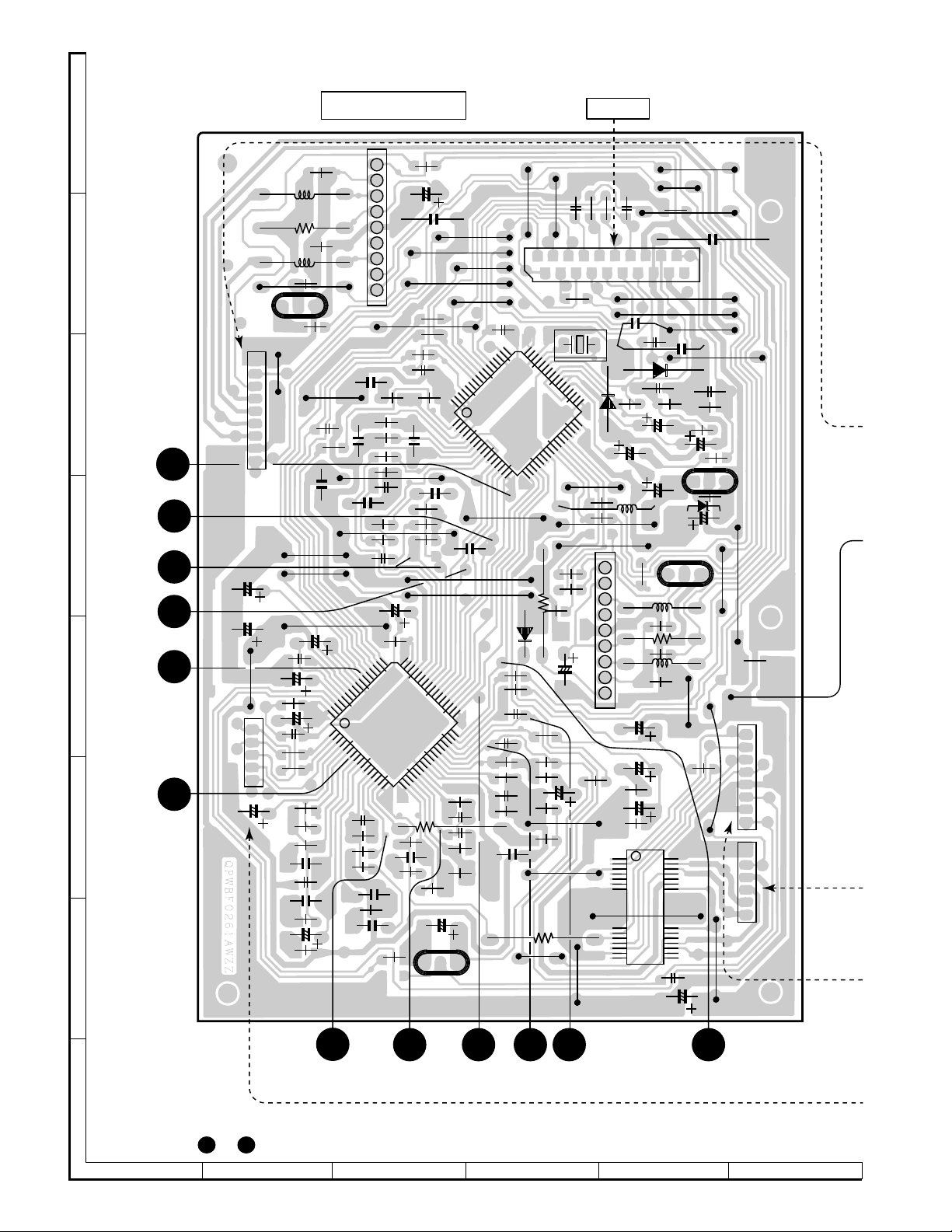
Figure 15 WIRING SIDE OF P.W.BOARD (1/7)
– 16 –
10 12
Page 17
CMS-R600X/R600XT
SUB PWB-C2
CNP90
1
2
3
PH2
CNS80A
CNS5
BK
1
BR
2
RD
3
OR
4
YL
5
GR
6
BL
7
GY
8
WH
9
TO POWER PWB
CNP901
P32 3 - A
CNS80B
1
23
RD(R)
M1
LOADING MOTOR
M
C1B C2B
COLOR TABLE
BR
BROWN
RED
OR
ORANGE
YL
YELLOW
GR
GREEN
BL
BLUE
TURNTABLE UP/DOWN
WH(W)
M2
M
VL
GY
BK
PK
VIOLET
GRAY
WHITE
BLACK
PINK
SW2
DISC UP
CNS2A
PICKUP UNIT
CD MOTOR PWB-D
-
M3
SPIN MOTOR
+
SW4
PICKUP IN
+
M4
SLIDE MOTOR
WH
PK
BL
YL
BK
CNS3BCNS3A
1
2
3
4
5
6
7
8
1
2
3
4
5
CNS2B
CNS4A
-
CNP4A
654321
RD
GY
WH
GY
WH
GY
1
2
3
4
5
6
CNS4B
1
2
3
4
5
6
1
2
3
4
5
6
7
8
PK
1
BL
2
BK
3
YL
4
WH
5
RD
WH
GY
WH
GY
WH
GY
WH
7
8 9 10 11 12
Figure 17 WIRING SIDE OF P.W.BOARD (2/7)
– 17 –
Page 18
CMS-R600X/R600XT
3
1
3
1
H
1
2
A
C2
47/10
R1
1K
C1
0.01
CNP2
CNS2A
CNS2B
F
5
4
B
3
LT0H30M1
ACTUATOR
A
2
E
1
K
LD
MON
K
E
B
LD GND
A
F
2200P
C
1M
2200P
1M
TR+
FO+
FO–
TR–
B
C
D
PICKUP UNIT
B
1
1
A
2
2
K
3
3
E
4
4
F
5
5
K
5
4
E
3
A
2
B
1
F
1
T–
2
T+
3
F+
4
F–
5
GND
6
+5V
7
VR
8
LD
C3
0.1/50
R4
2.2K
R5
6.8K
R6
100
R9
27K
0.047
R7
1K
R11
3.3K
R40
22K
C11
0.1
Q1
KTA1266 GR
4.9V
0V
C25
0.01
4.9V
R3
15K
R2
100K
C4
0.001
C5
0.033
C6
0.033
C7
0.1/50
C8
0.068
C9
C10
180P
R8
12K
R28
1K
R39
22K
R12
15K
R29
1K
+B
R43
22
1/50
C24
R42
560
FIN2
VCC1
1
FIN1
2
REF
E
3
F
REF
4
TB
5
REF
TE–
6
TE
7
REF
8
TESI
REF
SCI
9
TH
10
TA
11
TD–
12
REF
TD
13
+
–
REF
JP
14
TO
15
FD
16
R13
33K
C13
0.1
C40
0.33/50
LDS
LDD
–
+
–
+
–
+–+
VCR
–
+
VCR
–
+
+
–
REF
JP
REF
+
GEN
–
REF
+
GEN
–
REF
+
–
FD–
17 18 19 20 21 22 23 24 25 26 27 28 29 30 31 32
R14
10K
R15
47K
C39
BHI
PHI
RF
FE1
VCR
REF
–
VCR
+
+
–
+
–
TGL
THDL
FSC
FOSTA
FE1
GEN
REF
REF
+
–
+
–
AGND
FE–
FA–
FE
FA
C12
330P
R17
C14
0.01
R16
1.5K
0.01
C38
0.47/50
VR
LF2
REF
+
–
–
+
+
–
IC1
LA9240M
SERVO AMP.
VCC
+
–
+
–
GL
THD
S. Q. R.
+
–
REF
+
–
REF
SPI
SPG
SP
C15
0.0047
82K
R20
10K
R19
39K
+B
C37
C35
0.1/50
100/10
49505152535455565758596061626364
FSS
REFI
VCC2
+
–
DEF
HFL
DRF
REF
REF
PSTA
JP
SP–
C16
0.001
56K
R21
R22
6.8K
R23
1.2K
C17
0.47/50
CE
CL
CLK
DAT
DEF
DRF
EFBAL
FOSTA
TOSTA
2FREQ
LASER
FSTA
8/120M
SLOF
CV–
+
–
CV+
JP–
+
–
JP+
SLOF
OR
REF
TO
SLEQ
SPD
REF
47/10
C19
R25
1.2K
10K
R24
THLD
TBC
FSC
CLK
DGND
CE
CL
SLI
DAT
REF
P-ON RES
–
+
SLC
RFS–
REF
+
–
RFSM
RF
CV+
CV–
SLOF
HFL
+
–
TES
TOFF
TGL
+
–
JP+
SL–
SL+
SLD
JP–
R27
330K
R26
C18
1/50
330K
C20
0.0033
R41
4.7K
48
0V
47
2.5V
46
45
44
43
42
41
40
39
38
37
36
35
34
33
0.001
C45
4.7/25
C33
R33
5.6K
C50
0.1
R38
33K
C34
0.033
R36
47K
R37
47K
R34
C32
R32
1K
15P
56K
R35
C31
0.0027
C29
470
220P
CNP3
CNS3A
CNS3B
TR–
TR+
E
FO+
FO–
GND
PD
VR
LD
TO POWER PWB
CNP901
P33 6 - H
TR–
1
1
1
TR+
2
2
2
FO+
3
3
3
FO–
4
4
4
GND
5
5
5
PD
6
6
6
VR
7
7
7
LD
8
8
8
CNS5
1
2
FOCUS/TRACKING
/SPIN/SLIDE DRIVER
IC5
BA5920FP
F
CD MOTOR
PWB-D
+
M3
SPIN
MOTOR
SLIDE
MOTOR
SW4
PICKUP IN
M
–
M4
+
M
–
1
SP+
6
66
6
SP–
5
55
5
SL+
4
44
4
SL–
3
33
3
PUIN
2
2
22
GND
1
1
CNP4
CNS4A
CNS4B1CNP4A
G
H
• The numbers 1 to 12 are waveform numbers shown in page 36.
C21
0.47/50
R10
82K
NC
14
10111213
+
–
LEVEL
SHIFT
+
–
LEVEL
SHIFT
+
–
20
19
16
18
15
17
NC
NC
NCNCNC
89
–
+
+
–
+
–
VCC
VCC
21
22 232425
NC
+B
1234
567
–
+
–
+
LEVEL
SHIFT
LEVEL
SHIFT
+
+
–
–
26 27
28
NC
C48
PH2
RPI574N
DISC NO.
SENSOR
SUB PWB-C2
M1
LOADING
MOTOR
M2
TURNTABLE
UP/DOWN
SW2
DISC UP
470/10
M
M
33
22
1
1
CNP90
CNS80B
+
–
+
–
+B
C1B
4.7
C2B
4.7
CNS80A
1
2
3
4
5
6
7
8
9
C62
0.001
CNP80
GND
1
DISC NO. SENSOR
2
5.4V
3
+
4
–
5
+
6
–
7
GND
8
DISC UP
9
D
1SS
R59
150
L51
27µH
L54
27µ
L52
27µH
L53
27µH
1
23456
Figure 18 SCHEMATIC DIAGRAM (1/14)
– 18 –
Page 19
CMS-R600X/R600XT
7
8 9 10 11 12
CD PWB-C1
CD SIGNAL
C50
0.1
0.001
C54
SQOUT
ERROR
CORRECT
FLAG
CONTROL
R86
1K
RWC
CONT1
R87
FSX
WRQ
EXTERNAL
OUTPUT
CONT3
CONT2
1K
NC
CONT4
100P
SBCK
SUB-CODE
CONT5
R88
R89
1K
C22
0.01
NC
SFSY
X-TAL
GENERATOR
4FS
FILTER
DIGITAL
EMPH
29 30 31 3225 26 27 28
1K
NC
49505152535455565758596061626364
PW
1BIT
DAC
DIGITAL
DOUT
C2F
C29
220P
+B
+B
R62
2.2M
C41
0.047
C42
0.047
R57
27K
0.1
C49
R56
1.2K
R49
1K
R58
680
R60
1K
/CS
TEST5
TEST1
DEFI
1
TAI
2
PDO
3
SERVO/SIGNAL
VVSS
4
ISET
5
VVDD
6
FR
7
VSS
8
EFMO
9
SLICE
EFMIN
LEVEL
10
CONTROL
TEST2
11
CLV+
12
DIGITAL
CLV–
SERVO
13
V/P
14
HFL
15
SERVO
TES
COMMAND
16
TOFF
17 18 19 20 21 22 23 24
+B
NC
NC
16M
4.2M
TST11
LC78622E
CONTROL
VCO
CLOCK
OSC
CONTROL
CLV
JP–
JP+
TGL
/RES
/CQCK
µ-COM
INTERFACE
IC2
RAM
SYNC-DETECT
EFM DEMODULATE
FSEQ
PCK
NC
NC
COIN
VDD
R41
4.7K
C45
4.7/25
R38
33K
C34
0.033
C33
R36
47K
R37
47K
R33
5.6K
R34
C32
R32
1K
15P
56K
R35
C31
470
0.0027
+B
C60
C21
0.47/50
R10
82K
D2
1SS133
0.001
LDM L/H
LDM +
LDM –
TTM L/H
TTM +
TTM –
C55
C56
100P
100P
C57
100P
+B
NC
EFLG
48
NC
SBSY
47
46
XVSS
XIN
45
XOUT
44
XVDD
43
MUTER
RCHO
LCHO
MUTEL
OUT
TEST3
NCNCNC
RVDD
RVSS
LVSS
LVDD
TEST4
D7
42
NC
1SS133
0.0012
C63
41
40
39
38
37
36
35
34
NC
33
C61
0.001
D8
C43
220/10
1SS133
C68
10/16
C67
10/16
R82
100
0.82µH
L1
XL1
16.93MHz
R74
100
R76
10K
R75
10K
R73
100
C52
C69
100/10
C81
220/10
220P
C70
220P
KTC3203 Y
5V 5.7V
5.6V
CNS10
20
NC
19
L–CH
AGND
18
R–CH
17
GND
16
5.7V
15
+12V
14
SQOUT
13
COIN
12
CQCK
11
LDM L/H
10
SLDM–
9
SLDM+
8
RWC
7
6
RES
WRC
5
DRF
4
DISC NO.
3
SENSOR
2
PUIN
1
DISC UP
FC700
TO DISPLAY
PWB
P23 12 - C
Q81
R81
220
ZD81
MTZJ5.6B
C62
0.001
+B
IC51, IC52 : MOTOR DRIVER
Fusible
R95
3.9
9
IC51
TA7291S
7
2
6
8
5
C91
100/16
R99
12K
R91
10K
R97
6.8K
1
R59
150
3
L51
27µH
L54
27µH
Q51
KRC102 M
4V
23
1
0V
+B
0V
R93
1K
Fusible
R96
3.9
S80A
1
2
3
4
5
6
7
8
9
CNP80
GND
1
DISC NO. SENSOR
2
5.4V
3
+
4
–
5
+
6
–
7
GND
8
DISC UP
9
27µH
L52
27µH
L53
1
3
2
IC52
6
8
C92
100/16
9
TA7291S
75
R100
12K
R98
10K
Q52
KRC102 M
5V
0V
32
R92
12K
0V
1
R94
• NOTES ON SCHEMATIC DIAGRAM can be found on page 12.
+B
IC1
PIN
PIN
NO.
1
2
3
4
5
6
7
8
9
10
11
12
13
14
15
16
17
18
19
20
21
22
23
24
1K
25
26
27
28
29
30
31
32
VOLTAGE
2.5V
2.5V
2.5V
2.5V
2.5V
2.5V
2.5V
2.5V
2.5V
2.5V
2.5V
2.5V
2.5V
2.5V
2.5V
2.5V
2.5V
2.5V
2.5V
2.5V
2.5V
0V
2.5V
2.5V
2.5V
2.5V
2.5V
2.5V
2.5V
2.5V
2.5V
0V
NO.
33
34
35
36
37
38
39
40
41
42
43
44
45
46
47
48
49
50
51
52
53
54
55
56
57
58
59
60
61
62
63
64
VOLTAGE
0V
0V
0V
0V
0V
0V
0V
0V
1.6V
2.5V
2.5V
2.5V
0V
2.5V
0V
0V
0V
2.5V
4V
4V
0V
0V
5V
5V
2.5V
2.5V
1V
1V
2.3V
5V
0V
5V
PIN
NO.
1
2
3
4
5
6
7
8
9
10
11
12
13
14
15
16
17
18
19
20
21
22
23
24
25
26
27
28
29
30
31
32
VOLTAGE
0V
0V
2.7V
0V
2.3V
5V
1V
0V
2.5V
2.5V
0V
0V
0V
5V
0V
0V
5V
5V
0V
0V
–
–
5V
0V
0V
0V
0V
0V
–
–
–
0V
IC2
PIN
VOLTAGE
NO.
0V
33
–
34
–
35
5V
36
2.5V
37
0V
38
0V
39
2.5V
40
4.9V
41
–
42
5V
43
1.9V
44
2.2V
45
0V
46
–
47
–
48
–
49
–
50
–
51
–
52
0V
53
0V
54
0V
55
4V
56
4V
57
0V
58
–
59
–
60
2.5V
61
0V
62
0V
63
0V
64
PIN
NO.
10
11
12
13
14
15
16
17
18
19
20
21
22
23
24
25
26
27
28
VOLTAGE
1
2
3
4
5
6
7
8
9
IC5
3.5V
3.5V
2.5V
2.5V
0V
1.6V
0V
0V
2.5V
2.5V
3.5V
3.5V
0V
5.6V
0.7V
1V
3.5V
3.5V
2.5V
2.5V
5.6V
5.6V
2.5V
2.5V
2.5V
3.5V
3.5V
0V
PIN
NO.
PIN
NO.
1
2
3
4
5
6
7
8
9
1
2
3
4
5
6
7
8
9
IC51
VOLTAGE
0V
11.2V
5V
0V
0V
11.2V
5V
4V
0V
IC52
VOLTAGE
0V
11.2V
5V
0V
0V
11.2V
5V
5V
0V
Figure 19 SCHEMATIC DIAGRAM (2/14)
– 19 –
Page 20
CMS-R600X/R600XT
R794
R
A
TUNER
PRESET
TIME
R767
RESET
SW740
SW728
OPEN/CLOSE
SW708
DOWN
SW726
R799
R768
R798
R800
D708
R827
Q713
R837
E
C
B
R838
R845
Q707
E
C
B
R823
BAND
SW734
R841
R846
321
E
C
B
Q711
R843
Q708
600X
ONLY
R842
3
2
1
Q714
Q709
R829
R830
Q712
C708
RM703
RM704
E
C
B
R826
3
2
1
C704
R808
SW707
DISC SKIP
Q710
E
C
B
C712
R835
D703
R822
ZD701
C710
R839
R825
R817
C705
R833
ZD702
C713
R840
R819
BCE
Q705
R709
R806
R824
R818
R821
B
C
E
Q702
R707
R832
RX701
1
2
3
R831
D707
123
Q706
C706
1
FW703
3
1
FW703
SW718
UP
CNP701
132
3
B
C
D
VOLUME UP
Q703
R708
C707
B
C
E
R801
R706
D706
R719
SW706
DISC 5
R738
R740
R742
R701
R703
R702
ECB
R750
ECB
D701
Q704
R761
D702
R718
R704
Q701
R777
D705
R763
C715
R778
R779
XL702
R853
SW736
VIDEO/AUX
C716
L700
R854
SW705
DISC 4
C702
C703
R717
LMP802
R804
100
1
XL701
R783
R784
TAPE 1/2
SW737
R802
R815
R785
LCD701
1171819
2021222324252627282930313233343536
81
80
85
75
90
70
95
5
10
R786
15
R787
IC701
20
30
R788
25
R789
31
65
35
R791
60
40
R792
55
45
R793
E
SW735
VOLUME
DOWN
C709
R828
R834
1
FW851
R836
12
R770
R774
D704
R743
R744
R745
R772
R771
SW729
CLOCK/
TIMER
SW730
MEMORY/SET
LED701
PLAY
SW732
PLAY
LED703
FORWARD
SW717
FORWARD
F
CLOSE
RD
3
BK
2
BL
1
CNS701
TAPE
SPEED
VRM1
G
TAPE
SPEED
PHM1
1
2
RM1
4
3
MM1
TAPE MOTOR
SW801
CD CHANGER
OPEN
4
L
M
FWM1
H
R
WTM1
SWM4
F. A. S
1
123456789101112
12
SWM3
F. P.
1
SOLM1
SOLNOID
SWM5
CAM
1
FWM2
2
CNPM2
TAPE MECHANISM PWB-E
H
1
23456
Figure 20 WIRING SIDE OF P.W.BOARD (3/7)
– 20 –
Page 21

SWITCH PWB-B2
CMS-R600X/R600XT
LCD701
80
5
70
701
0
25
0
R789
R716
SW704
DISC 3
2021
65
60
51
55
50
45
40
35
31
R794
R793
R792
R791
SW738
TUNER
LMP801
R855
R803
SW703
DISC 2
R760
R715
12345678910111213141516171819
R757
R723
R710
R762
R711
C714
R741
CD
SW739
R739
R705
R736
R816
SW702
DISC 1
R735
R726
R727
3
2
1
R724
R725
R714
Q716
LED705
R758
R752
R753
R754
R755
R721
R722
987654321
CNP700
R749
R712
R713
TUNING
SW714
R751
P25 10 - A
TO MAIN PWB
CNP432
TUNING
R847
DOWN
SW722
D709
2019181716151413121110
X-BASS
SW713
D710
MEMORY
SW715
R848
SW710
R765
BGM
UP
R775
R732
R776
R734
R733
VOCAL
SW711
R737
HEAVY
SW712
POWER
SW716
16
14
12
10
8
6
4
2
15
13
11
9
7
5
CNS702
3
1
321
Q715
CD PAUSE
SW721
R747
R746
SW720
REC PAUSE
120
R748
SW724
TAPE EDIT
NORMAL
SW723
TAPE EDIT
HIGH
REWIND
SW725
LED702
REWIND
STOP
SW719
LED704
STOP
03
ARD
D
COLOR TABLE
BR
BROWN
RD(R)
WH(W)
OR
YL
GR
BL
VL
GY
BK
PK
RED
ORANGE
YELLOW
GREEN
BLUE
VIOLET
GRAY
WHITE
BLACK
PINK
120
CNS10
P16 5 - A
TO CD PWB
BCE
Q717
R849
R850
R851
R852
DISPLAY PWB-B1
FC700
R728
R729
R730
R731
FLAT
SW709
CNS703
10
9
8
7
6
5
4
3
2
1
CNP431
P25 10 - D
TO MAIN PWB
7
8 9 10 11 12
Figure 21 WIRING SIDE OF P.W.BOARD (4/7)
– 21 –
Page 22

CMS-R600X/R600XT
ADCONV GND
4
7
AVSS
O
S
O
5
COM3
A
B
SWITCH PWB-B2
R715
R714
12K
DISC 1 DISC 2 DISC 3 DISC 4 DISC 5
C
R728
39K
SW709 SW710
R743
39K
SW717 SW718
FORWARD
D
R716
6.8K
3.9K
SW704 SW705SW702
R729
R730
12K
6.8K
SW711 SW712 SW713 SW714
R745
R744
6.8K
12K
SW719 SW720
PRESET
STOP
UP
R767
39K
SW725
REWIND
R799
R798
6.8K
12K
R717
R718
2.7K
1.8K
R731
R732
3.9K
2.7K
X-BASS
R747
R746
2.7K
3.9K
SW721 SW722 SW723 SW724
CD
REC_
PAUSE
R768
18K
SW726
PRESET
DOWN
R800
3.9K
SW735SW734
VOLBAND
DOWN
PAUSE
SW728
VIDEO/
AUX
R770
3.9K
R801
2.7K
TUNING
5V
Q701
4.3V
KTA1266 GR
4.9V
Q702
KTA1266 GR
R706
R707
220
220
LED701
LED701 ~ LED704 : 5N4GTN52
R719
1.5K
SW708SW706 SW707SW703
DISC
OPEN/
SKIP
CLOSE
R733
R734
1.8K
1.5K
SW715 SW716
MEMORY
TUNINGFLAT BGM VOCAL HEAVY
UP
R748
R749
1.8K
1.5K
EDIT
DOWN
HIGH EDIT
R772
R771
3.3K
2.7K
SW730
SW729
(APMS)CLEARVOL UP
MEMORY
R802
R803
1.8K
1.5K
TAPE TUNER CD
1/2
5V
4.9V
R708
LED702
313
POWER
NORMAL
SW732
PLAY/
REPEAT
SW739SW738SW737SW736
4.3V
5V
Q703
KTA1266 GR
220
FW703
1
4.9V
R709
220
LED703
22K
R701
22K
4.3V
LED704
R723
10K
R737
10K
R758
10K
R774
10K
R806
10K
Q704
KTA1266 GR
R704
22K
R703
R702
22K
D701
1SS133
R738
4.7K
R740
16
18
33
32
R742
4.7K
282726 252423
31 30 29
R750
4.7K
TAPE SOL
TAPE MOTOR
<CE
>>DO
<TAPE HIGH SPEED
1K
R761
R763
P97
P96
P95
P94
P93
P92
P91
P90
P87
P86
P85
P84
P83
P82
P81
P80
SI0
R765
1K
1K
R775 ~ 779,
SEG20
81
SEG21
82
SEG22
83
SEG23
84
SEG24
85
SEG25
86
SEG26
87
SEG27
88
SEG28
89
SEG29
90
SEG30
91
SEG31
92
<ILLU GUIDE 1
93
<ILLU GUIDE 2
94
<ILLU GUIDE 3
95
<ILLU GUIDE 4
96
<TAPE SOL
97
<TAPE MOTOR
98
99
100
<<DI
1234
R775
R783 ~ 789,
R791 ~ 797 : 1K
SEG19
<CK
R776
222120
SEG17
SEG18
77
787980
>>SQOUT
R777
R778
SEG16
<CQCK
<<COIN
5
R779
SEG15
6789
35 34
36
4.7K
19
15
17
SEG10
SEG11
SEG12
SEG13
SEG14
73747576
707172
MICROCOMPUTER
XT1(SUB CLOCK)
IC(VPP)X2X1
VDD
101112 13 14
820
R804
4.19MHz
XL701
14
11 10
13 12
SEG5
SEG6
SEG7
SEG8
SEG9
6566
676869
IC701
IX0153AWZZ
SYSTEM
XT2(SUB CLOCK)
>TAPE 1 RUN PLSE
>REMOCON
>SYSTEM STOP
>RESET
16
15
R783
R784
9876
SEG2
SEG3
SEG4
64
<TAPE BIAS
>TAPE CAM SW
>TAPE FP
19 20 21 22
18
17
R785
R786
R787
5
SEG0
SEG1
616263
60
<PB MUTE
<T1/T2
<TAPE REC
R788
R789
R705
VLC2
59
VSS
<POWER
<S MUTE
23 24 25 26
R791
10K
R710
VLC1
5758
<LDM L/H
R792
10K
56
PHOT
<SLM–
R793
VLC0
LD C
R794
R711
55
BIAS
LD
DI
<SLM+
10K
2
4.3V
5V
4.9V
+B
C716
XL702
32.768kHz
Q712
0V
R843
10K
R854
150K
1
R853
10M
C702
47/16
C703
0.01
R815
10K
+B
+B
32
0V
+B
L700
2.2µH
SYSTEM STOP
C707
0.01
R821
D706
1K
R831
3.3K
1SS133
2
5V
1
Q706
KRC102 M
0V
3
0V
R832
100K
C706
3.3/50
C708
0.01
D707
1SS133
12P
C715
11.2V
2
R825
10K
R826
2.2K
KRC102 M
0V
Q708
1
1
0V
3
0V
Q714
KRC102 M
+B
10K
R841
32
0V
33P
KRC102 M
11.2V
R842
3.9K
R808
0V
D708
Q707
10K
D703
0V
1SS133
R823
0V
33K
R830
1K
Q711
KTA1270 Y
11.2V
0V
R835
11.2V
10K
C710
47/16
Q713
R840
KTA1270 Y
10
11.2V
0V
R845
11.2V
10K
11.2V
R846
2.2K
INITIAL RESISTOR
RM703
E
F
VRM1
L
MM1
TAPE
MOTOR
SWM4
F.A.S
G
SOLM1
SOLENOID
SWM5
CAM
H
+
M
–
FWM1
SWM3
F. P.
CNPM2
FWM2
TAPE MECHANISM
3.3K(B)
31
42
TAPE
SPEED
MOTOR
PHM1
RUN PALS
SENSOR
T2 RUNPALS
FULL PROOF
T1 RUNPALS
SOLENOIDO
MECHA STOP
PWB-E
RM1
FW851
2.7K
WTM1
1
L
2
H
3
GND
4
+B
5
6
7
8
9
10
11
12
600X : 33K
600XT : 10K
RM704
33K
600X ONLY
KTA1266 GR
R827
6.8K
1
1SS133
12
H
• NOTES ON SCHEMATIC DIAGRAM can be found on page 12.
1
23456
Figure 22 SCHEMATIC DIAGRAM (3/14)
– 22 –
Page 23

CMS-R600X/R600XT
16
14
15
11 10
13 12
17
SEG10
SEG11
702
7/16
703
.01
SEG12
9
R804
SEG6
SEG7
SEG8
SEG9
676869
707172
IC701
IX0153AWZZ
SYSTEM
MICROCOMPUTER
XT2(SUB CLOCK)
XT1(SUB CLOCK)
>TAPE 1 RUN PLSE
>REMOCON
>SYSTEM STOP
VDD
>RESET
101112 13 14
15
820
R783
4.19MHz
XL701
9876
SEG3
SEG4
SEG5
6566
64
>TAPE CAM SW
>TAPE FP
16
18
17
R784
R785
R786
SEG1
SEG2
616263
<T1/T2
<TAPE REC
<TAPE BIAS
19 20 21 22
R787
R788
5
SEG0
60
59
<S MUTE
<PB MUTE
R789
R705
10K
R710
VLC1
VLC2
5758
VSS
<LDM L/H
<POWER
23 24 25 26
R791
R792
4321
10K
R711
10K
COM2
56
5354
55
BIAS
VLC0
COM3
LD OPEN SW<
LD CLOSE SW<
DISC UP SW<
PUIN SW<
PHOTO SIGNAL<
WRQ<
RWC>
AVREF
ADCONV GND
<SLM–
<SLM+
>KEYIN 1
AVSS
27
28 29
R793
R794
COM0
COM1
5152
DRF<
VSS
RES>
AVDD
>KEYIN 2
30
>KEYIN 3
LCD701
R712
1K
TUN MUTE
50
PASS
49
SRS 1
48
R724
47
1K
46
45
R727
44
1K
43
42
41
R736
40
1K
39
38
ADCONV REF VOLT
37
ADCONV PWR SPLY
36
T2 RUN PALUS
35
34
33
R762
32
10K
31
KEYIN 4<
KEYIN 5<
R739
1K
INTIAL 1<
INTIAL 2<
R760
LMP801
LMP802
+B
1K
R757
CD SIGNAL
DISPLAY PWB-B1
+B
R713
R725
1K
R721
1K
R722
1K
1K
R726
1K
R735
100K
C714
0.022
R741
1K
+B
R751 ~ R755 : 10K
R751
R752
R753
R754
R755
R848
R855
220K
R847
10K
10K
+B
+B
D709
1SS133
D710
1SS133
+B
+B
1K
Q717
R849
KTA1271Y
8.2
R850
8.2
R851
2.2K
+B
R852
2.2K
Q715
KRC102M
312
+B
CNP701
CNP700
CNS703
NC
NC
CD CHANGER
1
1
2
2
3
3
CNS701
DISC UP
1
PUIN
2
DISC NO.
3
SENSOR
DRF
4
WRQ
5
RES
6
RWC
7
SLDM+
8
SLDM–
9
LDM L/H
10
CQCK
11
COIN
12
SQOUT
13
+12V
14
5.7V
15
GND
16
R–CH
17
AGND
18
L–CH
19
20
CNS702
CD_L
1
CD AGND
2
CD_R
3
CD SEC GND
4
CD SEC 5.7V
5
MECHA +12V
6
TUN MUTE
7
PASS
8
SRS
9
10
TUN_CL
11
TUN_DI
12
TUN_DO
13
TUN_CE
14
SRS SWITCH
15
16
POWER
1
N. C
2
PB.MUTE
3
T1/T2
4
TAPE REC
5
TAPE BIAS
6
GND
7
+12V LCD LAMP
8
9
HIGH SPEED
10
SPANSEL
OPEN
GND
CLOSE
SW801
FC700
CNP10
TO CD SERVO
PWB
P19 12 - D
TO MAIN PWB
CNP432
P26 3 - E
TO MAIN PWB
CNP431
P26 3 - F
L700
2.2µH
SYSTEM STOP
C707
0.01
R821
D706
7
1K
R831
3.3K
1SS133
2
5V
1
Q706
KRC102 M
0V
3
0V
R832
100K
C706
3.3/50
C708
0.01
D707
1SS133
+B
IC701
2.5V
0V
5V
5V
5V
5V
5V
0V
0V
5V
5V
5V
0V
0V
0V
0V
4.3V
0V
0V
0V
0V
5V
0V
0V
0V
PIN
NO.
51
52
53
54
55
56
57
58
59
60
61
62
63
64
65
66
67
68
69
70
71
72
73
74
75
VOLTAGE
2.5V
2.5V
2.5V
2.5V
5V
5V
3.3V
1.7V
0V
2.5V
2.5V
2.5V
2.5V
2.5V
2.5V
2.5V
2.5V
2.5V
2.5V
2.5V
2.5V
2.5V
2.5V
2.5V
2.5V
PIN
NO.
76
77
78
79
80
81
82
83
84
85
86
87
88
89
90
91
92
93
94
95
96
97
98
99
100
VOLTAGE
2.5V
2.5V
2.5V
2.5V
2.5V
2.5V
2.5V
2.5V
2.5V
2.5V
2.5V
2.5V
2.5V
2.5V
2.5V
2.5V
4.9V
4.9V
4.9V
4.9V
0V
0V
0V
0V
5V
5V
Q709
KTC3199 GR
0.4V
82
R838
R822
1K
10K
R829
0.4V
0.4V
KTC3199 GR
Q710
+B
R816
680
+B
LED705
5N4GTN52
R817
D705
Fusible
R818
(1/4W)
R828
R834
1SS133
R836
470
680
10
11V
6.3V
5.7V
Q705
2SD468 C
D704
1SS133
C709
150
1000/6.3
RESET
330
SW740
+B
D702
+B
10K
R824
0.4V
ZD702
MTZJ3.9B
1.1V
R833
100
1K
R837
10K
R839
1SS133
REMOTE SENSOR
RX701
321
C712
47/16
C713
0.01
2
1
C704
0.022
R819
100
C705
47/16
3
ZD701
MTZJ6.2C
KRC102M
Q716
PIN
NO.
10
11
12
13
14
15
16
17
18
19
20
21
22
23
24
25
VOLTAGE
1
2
3
4
5
6
7
8
9
PIN
VOLTAGE
NO.
0V
26
0V
27
0V
28
4V
29
4V
30
0V
31
2V
32
2.5V
33
5V
34
0V
35
–
36
5V
37
5V
38
5V
39
0V
40
0V
41
5V
42
0V
43
0V
44
5V
45
5V
46
0V
47
5V
48
0V
49
2.5V
50
8 9 10 11 12
Figure 23 SCHEMATIC DIAGRAM (4/14)
– 23 –
Page 24

CMS-R600X/R600XT
R446
R434
5
9
R
A
AM LOOP ANTENNA
2
1
1
C391
C393
Q302
C326
C328
C324
VD302
C331
VD331-1
L303
C339
R287
B
C
E
R318
R320
C325
R334
C342
C337
T333
L282
L281
B1
C
E
R284
Q282
SO301
ANTENNA
TERMINAL
B
FM 75ohms
GND
ANTENNA
C
2
1
RIGHT
PHONO
LEFT
SO401
RIGHT
D
VIDEO/
AUX
LEFT
SW421
PHONO
VIDEO/AUX
AB
CNP301
600X
ONLY
R425
D301
D332
C301
R426
BF301
321
C401
C315
D303
D302
C402
R312
C314
C313
C319
R401
C312
1
D331
C344
C316
C320
600X
ONLY
R403
L302
T331
R421
R422
C423
C318
R313
R404
IC301
432
VD301
R402
600X
ONLY
C317
R311
BF301
R316
C421
C422
C322
98
765
T301
C321
C323
R319
600X:JUMPER
600XT:L421
600X
ONLY
R314
R317
E
100/10
SW291
SPAN
SELECTOR
50/9
R499
R315
R339
2
3
R285
C327
C340
VD331-2
Q283
C332
R333
R286
C336
C281
R283
X381
C390
R388
TP301
R331
C282
B
C
E
Q281
CNS202
C386
22
R282
C388
20
R390
C385
FM MUTE
LEVEL
R281
C283
R386
C387
RD
C384
L351
Q273
Q274
CNP202
WH
IC381
15
L381
R387
VR351
C350
CF302
1
23
R351
C355
C353
1
2
3
1
Q208
2
3
1234567
R277
R276
R208
4567
YL
BKBKBK
R381
C356
R212
23
WH
Q201
R209
R210
C204
E
C
B
RECORD/PLAYBACK HEAD(55)
F
PLAYBACK HEAD(55)
L-CH
R-CH
WH
PK
G
CNS201
GY
TAPE 1
L-CH
123
BK
PK
WH
R-CH
ERASE HEAD(56)
WH
RD
YL
BK
WH
BK
GY
BR
TAPE 2
R394
11105
C383
R384
12
R389
C389
CF351
T351
1
C364
2
3
CF352
R353
C354
C74
1
5
IC351
C351
R352
24 20 15
C352
C358
C359
R354
Q202
123123
R201
C206
C205
123
R213
CNP201
B
B
C202
C201
C207
C
C
E
E
C208
Q207
R214
R238
C203
C214
R237
E
E
C
C
B
B
Q206
Q203
Q204
R205
R206
1
C
C357
E
B
R395
Q381
Q205
R393
R360
E
C
B
C363
R355
TP302
R215
R211
R216
R207
C216
Q272
R391
R356
R218
R396
1210
13
B
C
E
R364
R383
C213
C210
C209
1
R202
24
C214
C365
C368
C362
C218
R275
R399
R382
C381
X351
C215
C211
C212
R359
R357
R358
R217
R220
C242
ZD351
C367
C372
C366
C217
C219
5
C220
R222
R392
L355
C360
R225
IC201
R226
C284
R366
C371
C370
R363
C369
Q371
C221
R221
R219
C233
C251
C252
10 12
1520
C228
C236
R230
C226
C224
R224
C222
R228
600X
ONLY
FW562
31
SW561
3D SURROUND
R365
R375
C375
R235
13
C373
B
C
E
C377
C235
L202
R232
D351
C243
R288
R229
C227
C247
R245
R236
R377
C376
R234
R361
R379
B
C
E
C378
C241
C223
R223
C232
C234
R362
R374
R376
C225
C245
Q210
Q372
R378
L201
Q213
123
123
C230
R227
R244
R231
R248
R251
C229
R274
R246
R239
Q256
C231
Q211
B
C
E
E
C
B
B
C
E
600X
ONLY
R233
C253
C238
Q212
C433
C438
R452
123
C237
R249
600X
ONLY
R240
C431
C434
R255
R253
R241
R254
R256
COLO
BR
RD(R)
OR
YL
GR
BL
VL
GY
WH(W)
BK
PK
Q20
C432
R440
R438
C482
Q2
B
SWITCH PWB-D2
H
1
23456
Figure 24 WIRING SIDE OF P.W.BOARD (5/7)
– 24 –
Page 25

C237
C438
600X
ONLY
R452
123
R240
R249
C431
C434
R253
R254
R241
R255
R256
C432
Q209
Q255
R440
R438
C482
R434
R446
R432
ECB
R442
C444
R461
C440
C436
R448
C446
600X
ONLY
R444
C442
R462
R450
R272
R242
R436
R460
R435
R433
20
25
30
32
33
35
40
45
C448
C450
C456
C452
CNP601
R271
TO POWER PWB
R441
R439
17
IC431
48 49
C458
C454
CNS601
P32 6 - D
MAIN PWB-A1
R443
C437
C439
R431
R437
16
R445
15
10
5
1
64
600X
60
ONLY
55
50
C471
C466
C460
C464
C468
C475
C462
R454
321
9
8
7
TO POWER PWB
R447
600X
ONLY
C457
C455
C465
C476
D431
R453
C467
WT921
6
5
4
3
FW901
P32 5 - B
R449
2
C463
1
C481
C441
C453
C461
C451
R451
C445
C435
C449
C459
C443
C447
600X:JUMPER
600XT:D432
WT701
C478
R490
R489
C477
12345
P21 12 - B
TO DISPLAY PWB
CNS702
R488
C483
R487
9
FW501
1
16
14
12
10
CNP432
CNP431
10
Q483
E
C
Q481
B
CMS-R600X/R600XT
C525
15
13
11
9
8
7
6
5
4
3
2
1
FW501
9
9
8
7
WT501
6
5
4
3
2
1
1
9
8
7
6
5
4
3
2
1
1
2
3
R483
R481
CNS703
P21 12 - F
TO DISPLAY
PWB
C547
R549
C503
C551
R547
R515
C557
C546
C553
R516
C542
C544
C545
C543
C549
510
IC501
2520
R548
C556
C554
C552
R554
C558
C550
CMS-R600X ONLY
C524
R544
R543
R542
R541
C541
114
C523
C521
C505
C506
2815
R502
R552
G
D
Q502
S
C502
SRS PWB-E
1
R546
R545
Q501
R558
C504
E
C
R509
B
Q506
1
1
2
2
3
R501
R531
R557
R556
3
Q504
R533
C501
5
COLOR TABLE
BR
BROWN
RD(R)
RED
OR
ORANGE
YL
YELLOW
GR
GREEN
BL
BLUE
VL
VIOLET
GY
GRAY
WH(W)
WHITE
BK
BLACK
PK
PINK
7
R571
LED569
LED567
LED565
LED563
LED561
R561
C561
9
8
R567
7
6
5
4
IC561
3
2
1
C567
R569
C565
R563
C569
FW561
5
1
L563
R562
R564
3
C566
C562
R568
C568
R570
1
FW562
LED570
98
LED568
7
6
LED566
5
4
IC562
LED564
3
21
LED562
R572
R566
R565
LEVEL METER PWB-D1
8 9 10 11 12
Figure 25 WIRING SIDE OF P.W.BOARD (6/7)
– 25 –
LMP561
Page 26

CMS-R600X/R600XT
N
2
A
FM SIGNAL
B
C
D
E
F
PLAYBACK SIGNAL
RECORD SIGNAL
CD SIGNAL
VIDEO/AUX SIGNAL
VOLTAGE
1
2
3
4
5
6
7
8
9
PIN
VOLTAGE
NO.
5.6V
5.6V
5.6V
5.6V
5.6V
5.6V
5.6V
5.6V
5.6V
5.6V
5.6V
5.6V
5.6V
5.6V
5.6V
5.6V
5.6V
17
0V
18
5.6V
19
0V
20
5.6V
21
0V
22
0V
23
0V
24
0V
25
0V
26
0V
27
5.6V
28
0V
29
5.6V
30
0V
31
5.6V
32
PIN
NO.
10
11
12
13
14
15
16
IC431
PIN
NO.
33
34
35
36
37
38
39
40
41
42
43
44
45
46
47
48
VOLTAGE
5.6V
5.6V
5.6V
5.6V
5.6V
5.6V
5.6V
5.6V
5.6V
5.6V
5.6V
5.6V
5.6V
5.6V
5.6V
5.6V
PIN
NO.
49
50
51
52
53
54
55
56
57
58
59
60
61
62
63
64
VOLTAGE
5.6V
5.6V
5.6V
0V
5.6V
0V
5.6V
5.6V
11V
5.6V
0V
5.6V
0V
5.6V
5.6V
5.6V
SO401
L-CH
VIDEO/AUX
R-CH
CHASSIS
L-CH
PHONO
R-CH
P23 12 - D
CNS702
TO DISPLAY PWB
P23 12 - E
CNS703
TO DISPLAY PWB
SO401
CNP432
1
2
3
4
5
6
7
8
9
10
11
12
13
14
15
16
1
2
3
4
5
6
7
8
9
10
CNP431
600X ONLY
R425
560
R426
560
600X ONLY
CD L
A GND
CD R
SERVO GND
SER B +5.7
MECHA 12V
TUN MUTE
PASS
SRS
NC
CL
DI
DO
CE
SRS MODE
NC
POWER CONT
S MUTE
PB MUTE
T1/T2
TAPE REC
BIAS
GND(D)
LMP +B
SD(HIGH SP)
600X ONLY
VIDEO/ AUX
VIDEO/ AUX
C401
330P
C402
330P
R487
15K
R488
15K
PHONO
PHONO
R401
220K
600X ONLY
R402
220K
600X ONLY
C477
220P
C478
220P
R489
2.7K
R490
2.7K
R421
R422
47K
600XT ONLY
47K
SW421-A
SW421-B
SW291
SPAN
SELECTOR
0.82µH
R403
3.3K
R404
3.3K
L421
50/9
100/10
600X ONLY
C423
470P
600XT ONLY
R499
27K
600X ONLY
C421
600X : 270P
600XT : 100P
C421
C422
270P
C483
0.01
REC
+B
+B
+B
+B
+B
PB MUTE
HI SP
T1/T2
BIAS
D GND
+12V
43214
5
TO DECK SECTION
P31 12 - B, C
PLAYR
A GND
9876
PLAYL
RECR
11
RECL
1210
DICEDO
CL
21
3
TO TU
P
G
H
• NOTES ON SCHEMATIC DIAGRAM can be found on page 12.
1
23456
Figure 26 SCHEMATIC DIAGRAM (5/14)
– 26 –
Page 27

CMS-R600X/R600XT
R449
600X : 15K
47K
47K
R440
R451
47K
1K
C440
22/16
17
18
19
20
21
22
23
24
25
26
27
28
29
30
31
32
C482
2.2/50
C439
22/16
600XT : 12K
L4
L3
NC
L2
NC
L1
VSS
CL
DI
CE
VSS
AVSS
R1
NC
R2
NC
R3
R4
33
R448
3.3K
C481
2.2/50
+B
R449
C443
0.47/50
3.3K
R447
180P
C441
1213141516
LT IN
LF1C1
L SELO
LI VIN 1
AUDIO PROCESSOR
RT IN
RF1C1
R SELO
RIN VIN 1
34 3536373839
C444
0.47/50
R450
C442
180P
+B
+B
+B
C447
C445
0.22/50
0.056
11
10
LF2C1
LF1C3
LF1C2
IC431
LC75394E
RF1C2
RF1C3
RF2C1
40 414243 44
C446
0.056
C448
0.22/50
R450
600X : 15K
600XT : 12K
89
LF2C2
RF2C2
C450
C449
0.01
0.01
7
LF2C3
RF2C3
6
C452
1/50
C451
1/50
LF3C1
RF3C1
C453
0.047
5
LF3C2
RF3C2
LF4C2
C454
0.047
4
45
LF3C3
12
LF4C3
RF3C3
C456
0.056
C455
0.056
3
46
LF4C1
LIN VIN 2
LVR OUT
RVR OUT
RIN VIN 2
RF4C1
LT OUT
RT OUT
RF4C2
47
C438
1/50
R437
R435
1K
R433
R431
1K
600X ONLY
R445
1K
R443
47K
R441
47K
R439
1K
47K
R461
1K
R442
47K
R438
1K
R444
R446
47K
C437
1/50
C431
1/50
C433
1/50
C435
1/50
R460
1K
C432
1/50
+B
+B
+B
C434
1/50
C436
1/50
R462
1K
R432
1K
R434
1K
R436
1K
600X ONLY
R452
1K
MAIN PWB-A1(1/3)
C457
0.0022
12
0.0027
C459
64
LFS
LVREF
63
62
61
60
LVR IN
C467
59
LTEST
10/16
58
C475
57
VDD
100/10
56
VREF
55
C466
54
RTEST
10/16
53
RVR IN
C464
52
100P
51
50
RVREF
RFS
49
C460
48
0.0027
RF4C3
C458
0.0022
C461
C462
100/10
100/10
C463
100P
C465
10/16
C468
10/16
+B
C476
C471
0.022
D431
D432
600XT ONLY
+B
220/16
1SS133
1SS133
600X
ONLY
R-CH
R454
R453
1K
1K
L-CH
D GND
+12V
A GND
ECK SECTION
31 12 - B, C
PLAYR
9876
PLAYL
7
RECR
11
RECL
1210
DICEDO
CL
D GND
4321
5
TO TUNER SECTION
P29 12 - F
Q481
+12V
A GND
MUTE
LOUT
9876
KTA1271 Y
11.5V
11V
11.7V
+B
L IN
ROUT
10
1
WT701
TO LEVEL METER
R483
2.2K
R481
2.2K
R IN
GND
FW561
P34 2 - H
PWB
Q483
KRC102 M
0.2V
SRS
EDGE
432
5
2
0V
LAMP
3
4.3V
1
MUTE
P-CONT
1
TO POWER PWB
A +B
A GND
432
FW921
P33 4 - H
MCA +B
MCA GND
5
D GND
CD +B
CD GND
9876
WT921
CNP601A
R OUT
A GND
L OUT
2
1
3
CNS601
P33 3 - H
TO POWER PWB
L OUT
AGND
+B 12V
R OUT
4321
P35 2 - H
TO SRS PWB
R IN
5
WT501
L IN
PASS
SRS1
9876
8 9 10 11 12
Figure 27 SCHEMATIC DIAGRAM (6/14)
– 27 –
FW501
Page 28

CMS-R600X/R600XT
AM RF
1
C350
A
B
C
D
SO301
ANTENNA
TERMINAL
FM 75ohms
AM LOOP
ANTENNA
GND
1
2
1
2
CNP301
FM SIGNAL
BAND PASS
FILTER
BF301
21
3
C312
18P
C301
0.001
D302
1SS133
D301
1SS133
C315
0.01
1SS133
D303
C313
1
FM RF
C314
6.8P
0.0047
2
RF
L302
C316
0.0047
3
C318
0.001
C317
4.7P
R311
R312
22
C319
MIX
4
100K
R313
0.022
AM SIGNAL
FM FRONT END
IC301
TA7358AP
B. A
6
5
C322
15P
KDV147C
VD301
T301
FM IF
33K
C321
0.022
0.001
C320
OSC
7
C323
33P
L303
C324
FM BAND
COVERAGE
R314
10
FM OSC
3.3P
R315
47K
KTC3194 Y
C325
Q302
R316
47
KDV147C
VD302
22P
R318
680
VCC
R317
1
T351
AM IF
98
C328
10K
R319
4.7K
R320
C326
0.022
10.7MHz
820
C327
100P
CF302
10/16
1
3
2
R351
6.8K
R352
5.6K
FM MUTE
LEVEL
VR351
L351
1mH
C352
0.022
12
FM IF
AM OSC
24
C351
C353
0.022
C354
0.022
IN
AM OSC IN
OUT
23 22
3.3/50
2
AM
MIX
FM AFC
2
C355
R331
68K
VD331-2
KV1236Z23F
C344
8.2P
VD331-1
KV1236Z23F
C336
18P
C339
0.047
R334
100K
C342
0.022
C337
18P
R333
100K
C340
470P
R339
4.7K
TP301
Q381
KTA1266 GR
R381
47K
R382
10K
C381
47/16
R384
12K
R383
5.6K
+B
AM TRACKING fL
T331
D331
E
1SS133
F
D332
1SS133
C331
0.022
C332
0.022
AM BAND
COVERAGE fL
AM ANT
AM OSC
T333
G
H
• NOTES ON SCHEMATIC DIAGRAM can be found on page 12.
1
23456
Figure 28 SCHEMATIC DIAGRAM (7/14)
– 28 –
Page 29

T351
AM IF
CMS-R600X/R600XT
R365
390
R366
390
+B
CF351
3
1
2
C374
0.022
0.022
C360
0.022
C362
C363
100/6.3
C364
22P
L355
100µH
ZD351
MTZJ5.1B
C370
100/10
0.022
C371
5.6K
R363
R364
5.6K
1
6 GR
R382
10K
C381
47/16
FM MUTE
LEVEL
R351
6.8K
L351
1mH
R384
12K
R352
5.6K
VR351
R383
5.6K
C352
0.022
+B
C354
12
IN
FM IF
AM OSC IN
OUT
AM OSC
24
23 222120 19
C351
C353
0.022
3.3/50
0.022
AM
MIX
FM AFC
C350
AM RF
C355
10/16
IN
0.022
C356
4
REG
AM IF
VSM
22/16
C383
0.022
L381
100µH
R353
5
IN
CUT
AM LOW
18
C357
0.022
GND
FM/AM
2.7K
CF352
10.7MHz
270
R355
7
ST
TP302
0.022
83
R354
3.9K
C385
1/50
FM
DET
C396
1/50
R386
10K
VCC
17
X351
R389
10
MPX
VCO
R357
1K
C387
0.01
C386
47/16
IF
R358
OUT
16
3.3K
56K
R388
1.5K
69
SD
OUT
C359
1/50
C358
0.001
C384
R387
150
+B
C365
IN
MPX
C367
2.2/50
0.001
11
PHASE
L-CH
15
C366
C376
C388
C368
1/50
OUT
1/50
0.018
0.001
14
R-CH
OUT
C377
1/50
C375
0.018
R390
2.2K
R399
12
10K
R359
3.3K
FM/AM
13
PHASE
PILOT
R356
10K
IC351
LA1832
FM IF DET.
C378
1/50
PLL
IC381
LC72131
12
IF IN
13
IO2
NC
14
15
AM IN
16
FM IN
17
VDD
18
PD
AIN
19
AOUT
20
VSS
21
22
X OUT
C390
12P
/AM IF
/FM MPX.
R375
3.3K
R376
3.3K
R391
4.7K
IO1
11
B04
10
9
NC
B02
8
B01
7
6
DO
5
CL
4
DI
CE
3
NC
2
1
X IN
X381
4.5MHz
C369
C391
KTC3199 GR
1/50
Q372
2.7K
R377
R360
1.8K
330P
C389
15P
C372
0.022
Q371
R379
10K
R361
1K
R362
33K
KTC3199 GR
R374
10K
R378
2.7K
R392
1K
R396
R393
R394
R395
R393 – R396 : 1K
D351
1SS133
C373
3.3/50
C392
0.001
10
R-CH
9
L-CH
8
MUTE
7
A GND
(A)
+B
+12V
6
DI
2
CE
3
DO
4
CL
1
D GND
5
P27 8 - G
TO MAIN SECTION
+B
MAIN PWB-A1(3/3)
7
8 9 10 11 12
Figure 29 SCHEMATIC DIAGRAM (8/14)
– 29 –
Page 30

CMS-R600X/R600XT
HI SP
R236
1
A
MAIN PWB-A1(2/3)
RECORD SIGNALPLAYBACK SIGNAL
R242
R237
22K
10K
B
C
D
E
TAPE1
PLAYBACK HEAD
L-CH
R-CH
PLAYBACK HEAD
L-CH
R-CH
ERASE HEAD
TAPE2
RECORD/
33
22
1
1
CNS201
CNP201
77
66
55
44
33
22
1
CNS2021CNP202
C201
470P
470P
C202
MARKING EXCEPT FOR( ) : PLAY.
3
(0V)
0V
(0V)
0V
3
0.7V
(–17V)
R205
3.3K
0.7V
(–17.6V)
R207
6.8K
0.7V
(–17.6V)
R208
6.8K
0.7V
(–17V)
R206
3.3K
REC
0V
0V
R202
R211
(0V)
(0V)
1K
10K
R201
1K
KTC3199 GR
0V
(0V)
(0.7V)
0V
R209
R210
10K
R212
KTC3199 GR
REC
180P
C203
C204
180P
C205
560P
C206
560P
Q205
Q201
KRC104 M
0V
(0V)
2
1
1
0V
(0V)
2
Q202
KRC104 M
Q203
KTC3200 GR
0V
(0V)
0V
(0V)
0V
(0V)
0V
(0V)
KTC3200 GR
Q206
KTC3200 GR
0V
(0V)
0V
(0V)
0V
(0V)
0V
(0V)
Q204
KTC3200 GR
R238
10K
Q207
(0V)
10K
10K
(0.7V)
0V
HI. SP
0V
(0V)
(0V)
Q208
( ) : REC.
C207
0.001
0.001
C208
0V
0V
330P
C209
R213
1K
123
24 23
R214
1K
C210
330P
C213
47/10
C211
330P
C212
330P
C214
47/10
R216
R215
56
C215
0.033
+
HIGH=T1
+
22
56
100K
R217
–
–
C216
R218
C220
1/50
0.033
100K
R219
3.9K
C218
R220
4
21
560P
3.9K
C217
560P
C219
1/50
R224
R223
R221
5.6K
R226
C222
5.6K
R222
33K
R241
68K
33K
10K
0.01
C221
0.01
R225
10K
5
20
C252
C251
0.022
19
6
3.3/25
R228
3.3K
470P
C223
R227
6.8K
R229
18
6.8K
R230
3.3K
7
C224
C225
0.001
C226
0.001
470P
R240
R231
R232
10K
560
8
17
560
R234
C229
R233
C227
22/16
C228
22/16
C230
0.027
0.027
R239
5.6K
C253
22/16
0V
1
(0V)
0.027
C231
2
0V
(0V)
Q209
100
KRC104 M
HIGH SPEED
SWITCHING
L201
1.8mH
–
+
HIGH=CHROME
+
–
L202
1.8mH
Q210
KRC104 M
C232
100
0.027
0V
0V
(0V)
(0V)
1
3
C233
1/50
0V
(0V)
32
Q211
0V
C234
KTC3199 GR
(0V)
1/50
F
Q272
KTA1266 GR
+B
(8.2V)
0V
11.2V
(7.6V)
11.2V
(8.2V)
R275
10K
C242
0.047
R276
10K
G
0V
(11.2V)
2
KRC104 M
0V
(0V)
Q273
REC
1
3
(0V)
+B
0V
R277
(0V)
1
3
4V
10K
2
0V
(11.2V)
Q274
KRC104 M
C284
220/16
R288
220
H
• NOTES ON SCHEMATIC DIAGRAM can be found on page 12.
1
23456
Figure 30 SCHEMATIC DIAGRAM (9/14)
– 30 –
Page 31

CMS-R600X/R600XT
R229
R230
C223
470P
3.3K
R227
6.8K
7
18
6.8K
C224
C225
0.001
C226
0.001
470P
R242
22K
R240
10K
C229
0.027
100
R233
560
R231
C227
22/16
8
HIGH=CHROME
17
C228
22/16
560
R232
100
R234
0.027
C230
R237
10K
R239
5.6K
C253
22/16
0V
(0V)
0.027
C231
2
0V
(0V)
Q209
KRC104 M
HIGH SPEED
SWITCHING
L201
1.8mH
–
+
+
–
L202
1.8mH
Q210
KRC104 M
C232
0.027
0V
(0V)
1
(0V)
1
C233
0V
3
1/50
0V
(0V)
32
Q211
0V
(0V)
C234
P. B. MUTE
0V
(0V)
0V
(0.7V)
0V
(0V)
KTC3199 GR
C235
0.0033
R244
HI. SP
R235
9
16
1/50
10K
R236
10K
10K
15
C237
0.022
R245
10K
C243
CrO2Nor/
ALC
C236
C241
0.082
R246
10K
(9V)
9V
22/16
14
RIPPLE
ALC
1110
R248
0.0033
R249
10K
0V
(0V)
1
2
Q213
KRC104 M
C245
220/10
13
12
1K
KTC3199 GR
0V
(0V)
0V
(0.7V)
C238
0.022
(0V)
0V
3
VCC
GND
Q212
0V
(0V)
P. B. MUTE
R274
4.7K
C247
0.022
IC201
AN7345K
REC. /P. B. AMP.
0V
(0V)
0V
(0V)
Q256
KTC3199 GR
REC MUTING
SWITCHING
KTA1270 Y
11.2V
(11.2V)
R251
470
R287
150
(1/2W)
C282
0.0039
0.027
C281
(0V)
(ML)
(ML)
0.7V
R254
10K
Q282
0V
(11.1V)
R281
47K
11.2V
(10.6V)
0.7V
R253
10K
BIAS
L281
1mH
0V
(0V)
R282
100K
(0.9V)
0V
(0V)
0V
(0V)
R284
4.7K
R285
4.7K
(6.5V)
R283
12
L282
330µH
Q255
KTC3199 GR
REC MUTING
+B
2
11.2V
(0V)
0V
BIAS OSC
KTC3203 Y
(0.4V)
0V
R271
1K
R255
100K
Q283
KRC104 M
1
0V
(0V)
Q281
3
R272
0V
1K
(4.3V)
C283
47/16
R286
1K
BIAS
R256
100K
4
T1/T2
3
HI. SPEED
11
REC R
12
REC L
1
REC
10
PRE L
9
PRE R
2
PB. MUTE
BIAS
5
8
AGND
6
DGND
+12V
7
PIN
NO.
1
2
3
4
5
6
7
8
9
10
11
12
13
14
15
16
17
18
19
20
21
22
23
24
P26 5, 6 - H
TO MAIN SECTION
IC201
VOLTAGE VOLTAGE
PLAY. REC.
0V
0V
0V
0V
0.6V
0.6V
2.7V
2.7V
0V
0V
0V
1.2V
0V
0V
0.6V
0.6V
2.7V
2.7V
2.7V
2.7V
0V
0V
0V
0V
5.6V
5.6V
3.4V
3.4V
0V
0V
2.7V
2.7V
0.6V
0.6V
0V
0V
0V
0.8V
0V
0V
2.7V
2.7V
0.6V
0.6V
0V
0V
0V
0V
7
8 9 10 11 12
Figure 31 SCHEMATIC DIAGRAM (10/14)
– 31 –
Page 32

CMS-R600X/R600XT
P17 8 - D
TO CD SERVO
PWB
CNS5
R941
R940
C607
R605
R923
Q930
C643
C608
R606
Q931
C927
1
CNP901
WH
1
600X
ONLY
9
2
CNS601
D903
D901
D650
D651
R604
C602
321
R601
R603
C601
C603
C604
C901
LUG601
FW921
BK
R602
WT601
123456
PK
R616
C609
C610
C611
C612
R615
A
C924
R925
BCE
R930
F921
R924
R607
C637
R929
R926
R612
C622
R610
R611
C621
D902
D904
R931
C926
C902
R609
BCE
123
ZD922
R650
R614
C904
C905
R613
ZD921
D921
R928
Q926
CB
R641
R645
C639
E
CB
E
CB
E
IC601
R927
D642
D641
Q923
ECB
Q927
Q925Q924
2468
101214
T250mA L 250V
C925
R646
13579111315
C606
R608
C605
C903
R643
C644
C634
R644
C635
R642
ECB
Q641
C921
C923
C922
B
C
D
C907
C906
LUG 901
D907
D905
D908
D906
T1.6A
L 250V
F903
TO TAPE MECHANISM
WIRE LUG(254)
1
TO MAIN PWB
WT921
P25 8 - E
9
1
6
C652
FW601
1
6
R630
R629
D602
D603
HEADPHONES PWB-A3
WH
BK
PK
1
2
3
CNS601B
TO MAIN PWB
CNP601
P25 8 - E
J601
HEADPHONES
F902
E
230-240V
220V
127V
110V
T.F.
F
F901
T3.15A L 250V
T901
POWER TRANSFORMER
T3.15A L 250V
R934
F601
T2.5A L 250V
F602
T2.5A L 250V
COLOR TABLE
BR
BROWN
RD(R)
RED
OR
ORANGE
YL
600XT
ONLY
G
600X
ONLY
POWER PWB-A2
H
SW901
VOLTAGE SELECTOR
127V 110V
220V 230-240V
1
2
SO901
AC INPUT
600X: AC110/127/220/
230-240 V
50/60 Hz
600XT: 220 V, 50 Hz
600X
ONLY
J901
DC SOCKET
FOR RP-R600
ONLY
DC12V
L-CH
R-CH
L-CH
SPEAKER
R-CH
TERMINAL
SO601
GR
BL
VL
GY
WH(W)
BK
PK
YELLOW
GREEN
BLUE
VIOLET
GRAY
WHITE
BLACK
PINK
1
23456
Figure 32 WIRING SIDE OF P.W.BOARD (7/7)
– 32 –
Page 33

CMS-R600X/R600XT
A
B
C
D
E
F
G
H
1
23456
0.7V
17V
27V
6.8V
0V
6.3V
0V
6.8V
6.3V
–27V
0V
27V
0V
0V
0V
0V
0V
7.1V
17V
6.5V
6.4V
17V5.7V
12.3V
17V
11V
11.7V
11.7V
12.3V
13V
17V
16V
0V
SPEAKER
TERMINAL
SO601
(ML)
CHASIS
VOLTAGE
600XT
ONLY
600X
ONLY
SELECTOR
SW901
50/60Hz
220/230–240V
600X:AC 110/127/
600XT:AC 220V
AC INPUT
230 – 240V
220V
127V
110V
SO901
R-CH
L-CH
GND
GND
–
–
+
+
T. F
T901
(ML)
TO MAIN PWB
CD GND
AUDIO GND
MECHA +B
AUDIO +B
CD +B
L 250V
L 250V
L 250V
(ML)
T2.5A L 250V
F602
T2.5A L 250V
F601
32
1
DC 12V
NC
CNP901
ONLY
FOR RP-R600
DC SOCKET
J901
(1/4W)
R934
2.2
Fusible
2.2K
R940
2.2K
R941
KTA1271 Y
Q931
KRC102 M
Q930
CNP601
TO MAIN PWB
3
2
CNS601
1
SWITCHING
R602
150K
R650
0.22
C612
0.22(ML)
C611
REGULATOR
Q923 ~ Q927 : VOLTAGE
T500mA L 250V
F921
GND
CHASSIS
P27 9 - G
WT921
TO CD SERVO
PWB
CNS5
(LOW : OFF)
10K
R641
N. C
(ML)
(ML)
(ML)
(ML)
(ML)
(ML)
(ML)
(ML)
HEADPHONES
FM SIGNAL
POWER PWB-A2
LUG 601
TO TAPE MECHANISM
1SS133
D650
1SS133
D651
IC601
987654321
VOLTAGE
NO.
PIN
1514131211
10
+B
+B
+B
1
3
2
BI601
1
DIGITAL GND
MECHA GND
600X ONLY
POW CONT
9
FW921
L IN
R IN
SIGNAL GND
R601
R601, R602
600X : 1K
600XT : 4.7K
10K
R642
8
7
6
11
9
14
12
13
1
15
5
10
4
2
3
POWER AMP.
HEADPHONES PWB-A3
6
51423
FW601
6
3
4
2
WT601
5
1
+B
POWER
TRANSFORMER
LM1876TF
IC601
MUTE B
+IN B
–IN B
STAND-BY B
STAND-BY A
GND A
GND B
MUTE A
–IN A
(1/2W)
330
R630
D901 ~ D904 : 1N5402M
D905 ~ D908 : 10E4FD
+IN A
R603
600X : 82K
600XT : 68K
OUT B
OUT A
VCC A
VCC B
VEE
0.022
C922
0.022
C923
0.022
C921
47/16
C926
47/16
C925
47/10
C924
10K
R924
33K
R926
47
R927
1K
R929
560
R931
560
R928
33K
R925
10/16
C927
1SS133
D921
MTZJ13C
ZD922
MTZJ8.2A
ZD921
KTC3199 GR
Q926
KTD2058 Y
Q923
KTD2058 Y
Q925
KTC3199 GR
Q927
T1.6A
F903
T3.15A
F901
0.22
C904
0.22
C905
0.047
C906
0.047
C907
3300/25
C903
D902
D901
D903
D904
D907
D908
D905
D906
0.001
C601
100K
R605
1K
R607
1K
R608
470P
C605
R610
470P
C606
100/35
C608
0.001
C602
100K
R606
22K
R612
39P
C622
1K
R614
100/35
C607
600X : 150
600XT : 220
600X : 150
600XT : 220
R609
22K
R611
1K
R613
39P
C621
0.22
C610
0.22
C609
330
R629
J601
T3.15A
F902
2200/35
C901
2200/35
C902
1
R615
1
R616
33/16
C644
39K
R644
KTC3199 GR
Q641
47
R930
1SS133
D603
0.01
C652
1SS133
D602
10K
R643
0.022
C635
0.1
C637
0.022
C639
0.1
C634
1SS133
D642
5.6K
R646
1SS133
D641
5.6K
R645
2.2/50
C643
0.1
C604
0.1
C603
KTD2058 Y
Q924
R604
600X : 82K
600XT :
68K
2
1
600X
ONLY
P27 3 - G
P18 2 - F
50 Hz
• NOTES ON SCHEMATIC DIAGRAM can be found on page 12.
Figure 33 SCHEMATIC DIAGRAM (11/14)
– 33 –
Page 34

CMS-R600X/R600XT
3D SURROUND
SW561
FW562
600X ONLY
IC561, IC562 : METER DRIVER
LEVEL METER PWB-D1
SWITCH PWB-D2
3
21
3
TO MAIN PWB
P27 9 - G
WT701
FW561
L IN
EDGE LAMP
R IN
GND
SRS
5
4
3
2
1
CHASSIS
9
8
7
6
5
4
3
2
1
9
8
7
6
5
4
3
2
1
VC1
VC2
VC3
VC4
GND
VC5
ROUT
RIN
VCC
21
VC1
VC2
VC3
VC4
GND
VC5
LOUT
LIN
VCC
LB1403N
IC561
LB1403N
IC562
LMP561
10K
R569
10/16
C567
22K
R564
22K
R563
0.001
C565
10K
R567
120
R565
120
R566
10/16
C568
10K
R570
333ITR4
LED569
10K
R568
5N4KTN52
LED567
5N4KTN52
LED565
5N4KTN52
LED563
5N4KTN52
LED561
333ITR4
LED570
5N4KTN52
LED568
5N4KTN52
LED566
5N4KTN52
LED564
5N4KTN52
LED562
0.001
C566
120
R572
120
R571
330/16
C569
330µH
L563
0.001
C571
0.22/50
C561
0.22/50
C562
18K
R561
18K
R562
600X ONLY
A
B
C
D
E
F
G
H
• NOTES ON SCHEMATIC DIAGRAM can be found on page 12.
1
23456
Figure 34 SCHEMATIC DIAGRAM (13/14)
– 34 –
Page 35

CMS-R600X/R600XT
A
B
C
D
E
F
G
H
1
23456
+B
+B
+B
SRS PWB-E
RECORD SIGNAL
SRS
1
2
3
4
5
6
7
8
9
10 11 12 13
14
28
27 26
25
24
23 22
21
20
19
18
17
16
15
R-IN
L-IN
MODE
C-OUT
C-IN
CL4
CL3
CL2
CL1
VREF
LOUT
ROUT
CR1
GND
TO MAIN PWB
P27 11 - G
FW501
SRS 1
PASS
L-IN
R-IN
+12V
L-OUT
R-OUT
A GND
9
8
7
6
5
4
3
2
WT501
1
(ML)
3.9K
R546
(ML)
(ML)
(ML)
(ML)
(ML)
(SL)
0.47/50
C551
(ML)
32
1
1
32
CHASSIS
A +12V
A GND
VREF
GND
VREF
VCC
PN-IN
PN-OUT
C1
C2
C3
C4
C5
C6
S-IN
S-OUT
CR4
CR3
CR2
SRS5250S
IC501
33K
R541
1.5K
R544
100K
R542
22K
R543
47K
R545
0.0047
C525
100/16
C504
0.022
C521
0.47/50
C524
0.001
C505
KRC102M
Q504
1K
R531
39K
R557
1K
R533
47K
R558
100/16
C556
0.22(ML)
C554
KRC102M
Q506
KTC3203Y
Q501
2.2K
R509
1K
R501
1K
R502
100/16
C523
4.7K
R554
100
R552
0.47/50
C552
0.47/50
C550
4.7K
R548
1K
R516
2.2/50
C558
1K
R515
2.2/50
C557
0.22
C553
0.47/50
C549
0.33/50
C547
1.2K
R549
4.7K
R547
390P
C546
0.0018
C545
0.0068
C544
0.022
C543
0.068
C542
0.22
C541
0.001
C503
2SK246GR
Q502
1K
R556
2.2/50
C501
2.2/50
C502
0.001
C506
CMS-R600X ONLY
Figure 35 SCHEMATIC DIAGRAM (14/14)
– 35 –
Page 36

CMS-R600X/R600XT
5ms
0.50 V
1
IC1 20 F.E
5ms
5.0 V
2
IC1 54 DRF
WAVEFORMS OF CD CIRCUIT
STOP PLAY
FOCUS SERCH
0.5ms
10.0 V
6
JP+
0.5ms
10.0 V
7
JP-
0.5ms
0.50 V
8
3
1
JP
0.5ms
1.00 V
9
TE
3
4
5
3
4
5
6
7
8
9
6
7
8
9
0.5ms
1.00 V
HF
0.5ms
5.0 V
HFL
0.5ms
5.0 V
TES
0.5ms
1.00 V
HF
0.5ms
5.0 V
HFL
0.5ms
5.0 V
TES
50ms
10.0 V
JP+
50ms
10.0 V
JP-
50ms
0.50 V
JP
50ms
1.00 V
TE
0.5ms
10.0 V
JP+
0.5ms
10.0 V
JP-
0.5ms
0.50 V
JP
0.5ms
1.00 V
TE
CUE
1
2
3
REVIEW
1
2
3
CUE
10
11
10
11
12
20ms
1.00 V
SPO
20ms
2.00 V
CLV+
50ms
1.00 V
SPO
50ms
2.00 V
CLV+
5s
100mV
SLD
PLAY
NORMAL DISC
TN0=01
PLAY
TCD-712 (140mm)
TN0=01
PLAY
TCD-712
1
6
7
8
9
50ms
10.0 V
JP+
50ms
10.0 V
JP-
50ms
0.50 V
JP
50ms
1.00 V
TE
REVIEW
12
0.5s
100mV
SLD
1
– 36 –
Page 37

LCD701 : RV-LX0019AWZZ LCD Display
COMMON
*1C0C1C2C3
CMS-R600X/R600XT
SEGMENT
S 0
S 1
S 2
S 3
S 4
S 5
S 6
S 7
S 8
S 9
S10
S11
S12
S13
S14
S15
S16
S17
S18
S19
S20
S21
S22
S23
S24
S25
S26
S27
S28
S29
S30
S31
* 2
– 37 –
Page 38

CMS-R600X/R600XT
TROUBLESHOOTING (CD SECTION)
When the CD does not function
When the CD section does not operate When the objective lens of the optical pickup is dirty,this section may not operate.Clean
the objective lens,and check the playback operation.When this section does not operate even after the above step is taken,check
the following items.
Remove the cabinet and follow the troubleshooting instructions.
"Track skipping and/or no TOC(Table Of Contents) may be caused by build up of dust other foreign matter on the laser pickup lens.
Before attempting any adjustment make certain that the lens is clean. If not, clean it as mentioned below."
Turn the power off.
Gently clean the lens with a lens cleaning tissue and a small amount of isopropyl alcohol.
Do not touch the lens with the bare hand.
• When the turntable fails to stop.
Is from5 V till 0V down pulse (approx. 300 ms) input into the
IC701 pin 43 when the turntable is rotating?
Yes
Is there following voltage input on the IC701 pin 45 in the
specific state?
When the CD mechanism is moved up: 0V
In other states: 5V
Check IC2 pins 26, 27 and 28, Q52 and IC52 and the periphery.
Yes
IC701 defective.
2.5V
5V
0V
• When turntable fails to move.
Is there following voltage input on the IC701 pin 45 in the
specific state?
When the CD mechanism is moved up: 0V
In other states: 5V
No
No
Check the PH2 and the wiring from the IC701 pin 43 to the
PH2.
Check the SW3 and the wiring from the IC701 pin 45 to the
SW3.No
Check the SW3 and the wiring from the IC701 pin 45 to the
SW3.
Yes
Is L output from the IC2 pin 27?
Yes
Is L output from the IC2 pin 26 during SEC when the disc skip
switch is pressed?
Yes
Is 4V output from the CNP80 pin 6 during operation stated
above?
Yes
Check turntable motor and turntable mechanism.
No
No
No
– 38 –
Check the wiring from the IC2 pin 27 to the IC52 pin 1 and
IC52 pin 3 to the CNP80 pin 6.
OK
IC52 defective.
Check the wiring of IC2 pin 26 and Q52 pin 2.
OK
IC2 defective.
Check IC52 and the periphery.
Page 39

• When the CD tray fails to open or close.
0.5s
0.50 V
IC1 16 FD
2
1
0.5s
0.50 V
IC1 7 TE
Focus search is
performed two
times when play
operation is done
without disc.
CMS-R600X/R600XT
Is there following voltage input in specific state of IC701 pin
46 and 47 pin?
Open state: 0V (IC701 pin 47)
Close state: 0V (IC701 pin 46)
Intermediate state between open state and close state: 5V
Yes
Check the SW801 and the wiring from the IC701 pin 46 and
pin 47 to the SW801.
Yes
Is 4V output between IC51 pin 3 and pin 7 during operation
stated above?
Yes
Check the loading motor (M1) and the loading mechanism.
• The CD function will not work.
The CD operating keys don't work.
Yes
Check the CD, DSP, power supply, and 16.93 MHz clock, and
reset terminal.
No
No
No
Check the wiring of the IC2 pins 24 and 25, IC91 pins 1 and 3.
Is H output to IC2 pin 24 or 25 for 7 seconds when the OPEN/
CLOSE key is pressed? IC51 is defective. Replace it.
OK
IC2 defective.
Check the periphery of IC51.
OK
IC51 defective.
Yes
Check the waveform of SCK, SO (DATA) and SI (COMM).
Yes
See if the pick-up is in the pick-up in PICKUP IN SW position.
Yes
If the items mentioned above are OK, check the main
microcomputer IC701.
• The CD operating keys work.
Check the Focus - HF system.
Playback can be performed without a disc.
Yes
No
Does the output waveform of IC1(16)(FD) match that shown in
Fig. 39?
No
Yes
Yes
Focus search OKDoes the pick-up move up and down twice?
Check the area around IC5-CNP3.
Check the IC1(50)(CLK) line, 4MHz.
Check the microcomputer data on pins (51)(CL), (52)(DAT)
and (53)CE.
Figure 39
– 39 –
Page 40

CMS-R600X/R600XT
• Playback can only be performed when a disc
is loaded.
Is the Focus servo active? (Can you hear it working?)
Yes
No
Check the laser diode driver.
Check the area around IC1(16) - (21) (focus servo circuit).
Does the DRF signal change from "L" to "H"?
Yes
Is HF waveform normal (see the Fig. 40-1,2)?
Yes
Check the tracking system.
HF
1.0V/DIV
0.5µsec/DIV(DC)
(When playing
back the disc)
Figure 40-1
• Check the tracking system.
No
No
If the disc is not turning, the
DRF should not change to "H".
Level is abnormal.
Waveform is unstable. Check the spin system.
0.5s
1.00 V
16 FD
IC1
Yes
Check the spin system.
Yes
Check the periphery of
IC1 pins 41 and 42.
Yes
Waveform
in case
of normal
play-back
0.5s
10.0 V
12 CLV+
IC2
0.5s
10.0 V
IC1
54 DRF
2
1
3
4
0.5s
2.00 V
IC1 7 TE
Figure 40-2
Check waveform of IC1 pin 7 (TE).
Yes
The waveform shown in Fig.
40-3 appears, and no-disc
state appears soon.
Yes
Play is possible in
TEST mode.
Yes
Data cannot be read.
Yes Yes
Yes
Although IL is possible,
play is impossible.
5ms
1.00 V
IC1 7 TE
5 ms
5.0 V
IC1 54 DRF
Tracking servo is
inoperative.
Yes
Check the VCO-PLL system.
Yes
Check the periphery of IC 1
pin 8 to pin 15, and IC 5 to
CNP3.
Normal jump is impeded,
and the program top
cannot be reached.
4
3
Yes
Check the periphery
of IC 1 pin 14.
Figure 40-3
– 40 –
Page 41

• Checking the spin system.
Play operation is performed without disc.
Yes
CMS-R600X/R600XT
The turntable rotates a little.
No
The turntable fails to rotate or rotates at high speed.
• Checking the VCO-PLL system
Play operation is performed when disc exits.
Yes
Although HF waveform is normal, TOC data cannot be read.
0.5s
1.00 V
IC2 3 PDO
0.5s
1.00 V
IC1 16 FD
Yes
Yes
Yes
The spin driver circuit is normal.
Check the periphery of IC1 pins 23 to 27, pin 39, and pin 40, IC2
pin 12 and pin 13, IC5 to CNP4.
Check PDO waveform (Fig. 41).
Abnormal
Check the IC1 pins 43 and 44, IC2 pins 3, 5, 7, 9, and 10.
Stop --> Play
As VCO freque-
ncy is locked at
4.32 M Hz, voltage
of PDO rises and
stabili- zes.
2
• Although HF waveform is normal and the time
indication is normal, no sound is emitted.
Check IC2 pin 48 (EFLG).
Yes
Check IC2 pins 37, 40.
Normal
Check IC431 and POWER AMP IC601.
Figure 41
No
3
Usually, the number of pulses of flawless disc is 100 pulses/sec
or less.
– 41 –
Page 42

CMS-R600X/R600XT
FUNCTION TABLE OF IC
IC2 VHiLC78622E-1:Servo/Signal Control (1/2)
Pin No.
1 DEFI Input Input terminal of defect detection signal (DEF). (Connected to OV when not used.)
2 TAI Input For PLL Input terminal for test. Pull-down resistor is integrated. Surely connected to 0V.
3 PDO Output Output terminal of phase comparison for external VCO control.
4 VVSS — Ground terminal for integrated VCO. Surely connected to 0V.
5 ISET Input Resistance connection terminal for current adjustment of PDO output.
6 VVDD — Power terminal for integrated VCO.
7 FR Input VCO frequency range adjustment.
8 VSS — Ground terminal of digital system. Surely connected to 0V.
9 EFMO Output For slice level control EFM signal output terminal.
10 EFMIN Input EFM signal input terminal.
11 TEST2 Input Input terminal for test. Pull-down resistor is integrated. Surely connected to 0V.
12 CLV+ Outout Output for disk motor control. 3 values can be output with the commands.
13 CLV- Output Output for disk motor control. 3 values can be output with the commands.
14 V/P Output Monitor output terminal for automatic switch of rough servo/phase control.
15 HFL Intput Input terminal of track detection signal. Schmit input.
16 TES Input Input terminal of tracking error signal. Schmit input.
17 TOFF Output Tracking OFF output terminal.
18 TGL Output Output terminal for switch of tracking gain "L" increases the gain.
19 JP+ Output Output for track jump control. 3 values can be output with the commands.
20 JP- Output Output for track jump control. 3 values can be output with the commands.
21* PCK Output Clock monitor terminal for EFM data replay. 4,3218MHz as the phase clock.
22* FSEQ Output Output terminal synchronous signal detection. "H" is output when synchronous signal
23 VDD — Power terminal of digital system.
24 CONT1 Input/Output General purpose input/output terminal 1
25 CONT2 Input/Output General purpose input/output terminal 2
26 CONT3 Input/Output General purpose input/output terminal 3
27 CONT4 Input/Output General purpose input/output terminal 4
28 CONT5 Input/Output General purpose input/output terminal 5
29* EMPH Output Difference monitor terminal At "H", deemphasis disk is being replayed.
30* C2F Output C2 flag output terminal.
31* DOUT Output Output terminal of digital OUTPUT. (EIAJ format)
32 TEST3 Input Input terminal for test. Pull-down resistor is integrated. Surely connected to 0V.
33 TEST4 Input Input terminal for test. Pull-down resistor is integrated. Surely connected to 0V.
34* N.C. — Terminal not used. Open during operation.
35* MUTEL Output L channel 1 bit DAC Mute output terminal for L channel.
36 LVDD — Power terminal for L channel.
37 LCHO Output L channel output terminal.
38 LVSS — Ground terminal for L channel Surely connected to 0V.
39 RVSS — R channel 1 bit DAC Ground terminal for R channel Surely connected to 0V.
40 RCH0 Output R channel output terminal.
41 RVDD — Power terminal for R channel.
42* MUTER Output Mute output terminal for R channel.
43 XVDD — Power terminal for quartz oscillation.
44 XOUT Output Ground terminal of 16.9344 MHz quartz oscillator.
45 XIN Input Ground terminal of 16.9344 MHz quartz oscillator.
46 XVSS — Ground terminal for quartz oscillation. Surely connected to 0V.
47* SBSY Output Output terminal of synchronous signal of subcode block.
48* EFLG Output Correction monitor terminal of C1, C2, single and double.
Input/Output
"H" for rough servo, and "L" for phase servo.
detected by EFM signal matches synchronous signal internally generated.
FunctionTerminal Name
Controlled with serial data command from micro
computer. When not used, set it as the input
terminal and open it by connecting to 0V, or set it
as the output terminal and open it.
In this unit, the terminal with asterisk mark (*) is (open) terminal which is not connected to the outside.
– 42 –
Page 43

CMS-R600X/R600XT
DEFI
EFMIN
FSEQ
V/P
PW
SBCK
SBSY
SFSY
CS
WRQ
SQOUT
COIN
RWC
CQCK
HFL
TES
TOFF
JP-
JP+
RES
TGL
CONT1
CONT2
CONT3
CONT4
CONT5
EMPH
EFLG
16M
4.2M
XVss
FSX
XIN
XOUT
XV
DD
RVss
RV
DD
MUTER
RCHO
LCHO
MUTEL
LVss
LV
DD
(NC)
DOUT
C2F
EFMO
VVDDVVss
PDO
I SET
FR
PCK
TAI
TSTI1
TEST1
TEST2
TEST3
TEST4
TEST5
VDDVss
CLV+
CLV-
Slice level
control
VCO colck oscillation
clock control
2K X 8bit
RAM
RAM address
generator
Interpolation mute
Bilingual
Digital OUT
Digital
attenuator
X4 oversampling
digital filter
1bitDAC
L.P.F
XTAL system timing
generator
General-use port
Servo commander
µCOM
Interface
Subcode division
QCRC
CLV
Digital servo
Sync detection
EFM demodulation
Flag processing of C1/C2
error detection and correction
IC2 VHiLC78622E-1:Servo/Signal Control (2/2)
Pin No.
Input/Output
49* PW Output Output terminal of subcodes P, A, R, S, T, U and W.
50* SFSY Output Output terminal of synchronous signal of subcode frame. It drops when subcode stands by.
51* SBCK Input Clock input terminal to read subcode. Schmit input (Connected to 0V when not used.)
52* FSX Output Output terminal of synchronous signal of 7.35kHz divided from quartz oscillation.
53 WRQ Output Output terminal to stand by output of subcode Q.
54 RWC Input Input terminal of read/write. Schmit input.
55 SQOUT Output Output terminal of subcode Q.
56 COIN Input Command input terminal from microcomputer.
57 CQCK Input Clock input terminal to fetch command input, or pick up subcode from SQOUT. Schmit input
58 RES Input Reset input terminal of LC78622. When turning on power, set it at "L".
59* TST11 Output Output terminal for test. Used in the open state ("L" output as ordinary).
60* 16M Output Output terminal of 16.9344Hz.
61 4.2M Output Output terminal of 4.2336MHz.
62 TEST5 Input Input terminal for test Pull-down resistor is integrated. Surely connected to 0V.
63 CS Input Chip selection input terminal. Pull-down resistor is integrated.
Connected to 0when not controlled.
64 TEST1 Input Input terminal for test Pull-down resistor is integrated. Surely connected to 0V.
Note: The same potential must be supplied to the power terminals (VDD, VVDD, LVDD, RVDD, XVDD).
In this unit, the terminal with asterisk mark (*) is (open) terminal which is not connected to the outside.
FunctionTerminal Name
IC2 VHiLC78622E-1:Servo/Signal Control
Figure 43 BLOCK DIAGRAM OF IC
– 43 –
Page 44

CMS-R600X/R600XT
IC1 VHiLA9240M/-1:Servo Amp. (1/2)
Pin No.
1 FIN2 Connection pin for photodiode of pickup.
2 FIN1 Connection pin for photodiode of pickup.
3 E Connection pin for photodiode of pickup. TE signal is generated through subtraction with F pin.
4 F Connection pin for photodiode of pickup.
5 TB Pin for input of DC component of TE signal.
6 TE- Pin to connect gain setting resistor of TE signal to TE signal.
7 TE TE signal output pin.
8 TESI TES (Track error sense) comparator input pin. TE signal is band-passed and input.
9 SCI Input pin for shock detection.
10 TH Pin to set time constant of tracking gain.
11* TA TA amplifier output pin.
12 TD- Pin to compose tracking phase compensation constant between TD and VR pins.
13 TD Pin to set tracking phase compensation.
14 JP Pin to set amplitude of tracking jump signal (kick pulse).
15 TO Tracking control signal output pin.
16 FD Focusing control signal output pin.
17 FD- Pin to compose focusing phase compensation constant between FD and FA pins.
18 FA Pin to compose focusing phase compensation constant between FD-/FA-pins.
19 FA- Pin to compose focusing phase compensation constant between FA and FE pins.
20 FE Output pin of FE signal.
21 FE- Pin to connect gain setting resistor of FE signal across TE pin.
22 AGND GND for analog signal.
23 SP Single end output for CV+ and CV- pin input.
24 SPI Spindle amplifier input.
25 SPG Pin to connect gain setting resistor in the 12cm mode of spindle.
26 SP- Pin to connect spindle phase compensation constant together with SPD pin.
27 SPD Spindle control signal output pin.
28 SLEQ Pin to connect thread phase compensation constant.
29 SLD Thread control signal output pin.
30 SL- Input pin of thread feed signal from micro computer.
31 SL+ Input pin of thread feed signal from micro computer.
32 JP- Input pin of tracking jump signal from DSP.
33 JP+ Input pin of tracking jump signal from DSP.
34 TGL Input pin of tracking gain control signal from DSP. TGL = Gain low at "H"
35 TOFF Input pin of tracking off control signal from DSP. TOFF = Off at "H"
36 TES Output pin of TES signal to DSP.
37 HFL (HIGH FREQUENCY LEVEL) is used to judge whether main beam is positioned on the bit or on the mirror.
38 SLOF Thread servo off control input pin.
39 CV- Pin to input CLV error signal from DSP.
40 CV+ Pin to input CLV error signal from DSP.
41 RFSM RF output pin.
42 RFS- Pin to set gain of RF and set 3T compensation constant together with RFSM pin.
43 SLC (SLICE LEVEL CONTROL) is the output pin to control of the level of the data slice with RF waveform DSP.
44 SLI Input pin to control the level of data slice with DSP.
45 DGND GND pin in the digital system.
46 FSC Output pin for focus search smoothening capacitor.
47 TBC (Tracking Balance Control) Pin to set EF balance variable range.
48* NC No connect.
49 DEF Defect detection output pin of disk.
50 CLK Reference clock input pin. 4.23MHz of DSP is input.
Port Name
RF signal is generated through addition with FIN pin, and FE signal is generated through subtraction.
In this unit, the terminal with asterisk mark (*) is (open) terminal which is not connected to the outside.
Function
– 44 –
Page 45

CMS-R600X/R600XT
IC1 VHiLA9240M/-1:Servo Amp. (2/2)
Pin No.
Port Name
51 CL Micro computer command clock input pin.
52 DAT Micro computer command data input pin.
53 CE Micro computer command chip enable input pin.
54 DRF (DETECT RF) RF level detection output.
55 FSS (Focus Serch Select) Pin to switch focus search mode. (± search/+ search for reference voltage)
56 VCC2 VCC pin for servo system and digital system.
57 REFI Pin to connect pass control for reference voltage.
58 VR Reference voltage output pin.
59 LF2 Pin to set defect detection time constant of disk.
60 PH1 Pin to connect capacitor for peak hold of RF signal.
61 BH1 Pin to connect capacitor for bottom hold of RF signal.
62 LDD APC circuit output pin.
63 LDS APC circuit output pin.
64 VCC1 RF system VCC pin.
Function
IC1 VHiLA9240M/-1:Servo Amp.
VCC1
DEFCLKCLDATCEDRFFSSVCC2REFIVRLP2PH1BH1LDDLDS
495051525354555657585961 60626364
FIN1
TESI
APC
1FIN2
2
I/V
3
E
4
F
5
TB
6
TE-
7
TE
8
9
SCI
BAL
TE
RF DET
VCA
VCA
T.SERVO & T.LOGIC
10
TH
11
TA
12
TD-
13
TD
F.SERVO & F.LOGIC SPINDLE SERVO SLED SERVO
REF
µ-COM
INTER FACE
SLC
RF AMP
48
NC
47
TBC
46
FSC
45
DGND
44
SLI
43
SLC
42
RFS-
41
RFSM
40
CV+
39
CV-
38
SLOF
37
HFL
36
TES
35
TOFF
34
TGL
JP+
33
14
JP
15
TO
16
FD
17 18 19 20 21 2322 25 26 27 28 29 30 31 32
FD-
FA FA-
FE FE- AGND SP SPI SPG SP- SPD SLEQ SLD SL- SL+ JP-
24
Figure 45 BLOCK DIAGRAM OF IC
– 45 –
Page 46

CMS-R600X/R600XT
IC701 RH-iX0153AWZZ:System Microcomputer (1/2)
Port Name Terminal NamePin No. Input/Output Function Active
1 SO0 C2B DI Output C2B Data output (Normal: LO) L/H
2 SCK0 C2B CK Output C2B Clock output (Normal: LO) L/H
3 RXD SQOUT Input CD Sub-Q data input L/H
4 TXD COIN Output CD System Command data output (Function "CD": H) L/H
5 ASCK CQCK Output CD Clock for system command (Function "CD": H) L/H
6 ICVPP — — GND —
7 X2 — Output System clock 4.19 MHz —
8 X1 — Input System clock 4.19 MHz —
9VDD — — +5V (Back-up) —
10 XT1 SUB CLOCK Input 32.768 kHz OSC —
11 XT2 SUB CLOCK Output 32.768 kHz OSC —
12 RESET RESET Input System reset L
13 INTP0 SYSTEM STOP Input System stop detection L: STOP L
14 INTP1 REMOCON Input Remocon serial data input L
15 P02 T1 RUN PLSE Input T1 Play detection H/L: Rotation fixed: STOP L/H
16 P03 TAPE FP Input T2 FP SW detection
17 P04 CAM SW Input Tape stop mode detection L: STOP L
18 P05 TAPE BIAS Outout TAPE Recording BIAS control H: BIAS OSC on H
19 P110 TAPE REC Output Record/Playback control H: Playback L: Recording L
20 P111 T1/T2 Output T1/T2 Mode selector H: T1 L: T2 L/H
21 P112 PB MUTE Output Playback muting L: Playback H: Mute ON H
22 P113 S MUTE Output System muting H: Mute ON H
23 P114 POWER Output Power control H: Power ON H
24 P115 LDM L/H Output Tray open/close motor speed control L: HIgh H: Low L/H
25 P116 SLM- Output CD Pick-up slide motor control H: To inside H
26 P117 SLM+ Output CD Pick-up slide motor control H: To outside H
27 AVSS — — AD converter GND —
28 - 32 ANI0 - 4 KEYIN 1 - 5 Input AD Input for key-in —
33 ANI5 INITIAL 1 Input AD Input for auto scan set 0V: Without auto scan —
34 ANI6 INITIAL 2 Input AD Input for tuner band See(KEY ARRANGEMENT TABLE) —
35 ANI7 T2 RUN PALSE Input TAPE2 Rotation detection
36 AV DD — — AD Converter +B(5V) —
37 AVREF — — AD Converter refarence voltage (5V) —
38 P100 RWC Output CD DSP Chip enable H
39 P101 RES Output CD DSP Reset L: Reset H
40 V SS V SS — GND —
41 P102 WRQ Input Write request from CD DSP H
42 P103 DRF Input Data read flug from CD DSP H: Focus OK H
43 P30 PHT Input CD Disc No. detection H
44 P31 PUIN SW Input CD Pick-up detection L: inside L
45 P32 DISC UP SW Input CD traverce mecha detection L: UP complete L
46 P33 CLOSE SW Input CD Tray close detection L: Close complete L
47 P34 OPEN SW Input CD Tray open detection L: Open complete L
48 P35 SRS 1 Output SRS mode control L: MODE1 H: MODE2 L/H
49 P36 PASS Output SRS ON/OFF control H: PASS L: SRS ON L/H
50 P37 TUN MUTE Output Tuner Muting H: Mute ON H
51 - 54 COM0 - 3 COM0 - 3 Output LCD Common drive out —
55 BIAS BIAS Output LCD Bias voltage output —
56 - 58 VLC0 - 2 VLC0 - 2 — LCD Bias voltage input —
59 V SS V SS — GND —
H: Recording inhibited L: Recording enabled
Voltage changing: Rotation
L/H
—
– 46 –
Page 47

CMS-R600X/R600XT
IC701 RH-iX0132AWZZ:System Microcomputer (2/2)
Port Name Terminal NamePin No. Input/Output Function Active
60 - 91 SEG0 - 31 SEG0 - 31 Output LCD Segment driver output —
92 P87 ILLU GUIDE 1 Output LED Control L: ON L
93 P86 ILLU GUIDE 2 Output LED Control L: ON L
94 P85 ILLU GUIDE 3 Output LED Control L: ON L
95 P84 ILLU GUIDE 4 Output LED Control L: ON L
96 P83 TAPE SOL Output Tape solenoid control H: Pull L: Release H
97 P82 TAPE MOTOR Output Tape motor control H: ON H
98 P81 HI SPEED Output Tape speed control H: Normal L: High L
99 P80 C2B CE Output C2B Chip enable output H
100 SI0 C2B DO Input C2B Data input L/H
KEY ARRANGEMENT TABLE
KEY POSITION
PORT VOLTAGE
PIN.NO.
(28) KEYIN 1 K01 K02 K03 K04 K05 K06 K07 K08 NO KEY
(29) KEYIN 2 K11 K12 K13 K14 K15 K16 K17 K18 NO KEY
(30) KEYIN 3 K21 K22 K23 K24 K25 K26 K27 K28 NO KEY
(31) KEYIN 4 K31 K32 K33 K34 K35 K36 K37 K38 NO KEY
(32) KEYIN 5 K41 K42 K43 K44 K45 K46 K47 K48 NO KEY
(33) AUTO SCAN INITIAL-1 INITIAL-2 NO KEY
(34) TUNER TUNER TUNER TUNER TUNER TUNER TUNER TUNER TUNER NO KEY
(35) T2 RUN NO KEY
ADDATA
PORT
(ANI 0) INPUT
(ANI 1) REPEAT APMS CLEAR VOL UP PRESET REWIND INPUT
(ANI 2) NOR EDIT HIGH EDIT TUNING CD PAUSE
(ANI 3) POWER PRESET TUNING UP X-BASS HEAVY VOCAL BGM FLAT INPUT
(ANI 4) OPEN/ DISC SKIP DISC 5 DISC 4 DISC 3 DISC 2 DISC 1
(ANI 5) w/o AUTO w/o AUTO INPUT
(ANI 6) USA EU 1 EU 2 JAPAN EX 1 EX 2 KOREA OIRT INPUT
PALUS INPUT
KN0 KN1 KN2 KN3 KN4 KN5 KN6 KN7 OPEN
0V(0.0) 0.65V(0.13) 1.24V(0.248) 1.88V(0.375) 2.49V(0.497) 3.13V(0.625) 3.71V(.0625) 4.36V(0.871) 5V(1.0)
CD TUNER TAPE 1/2 VIDEO
PLAY A RANDOM MEMORY DOWN
DOWN
MEMORY
CLOSE
SCAN SCAN
FM,MW FM,MW,LW 9K 10K
VOL DOWN
REC PAUSE
BAND SRS BAL L
STOP
PRESET UP
FF INPUT
BALANCE R
INPUT
– 47 –
Page 48

CMS-R600X/R600XT
IC5 VHiBA5920FP-1:Focus/Tracking/Spin/Slide Driver
Pin No.
1 VO1(-) Driver CH1 Negative output.
2 VO1(+) Driver CH1 Positive output.
3 VIN1 Driver CH1 input.
4* VIN1' Input terminal to adjust driver CH1 gain.
5* NC Not Used
6* NC Not Used
7 MUTE Mute control terminal.
8 GND GND
9 VIN2' Input terminal to adjust driver CH2 gain.
10 VIN2 Driver CH2 input.
11 VO2(+) Driver CH2 Positive output.
12 VO2(-) Driver CH2 Negative output.
13 GND Substraigth GND.
14* OP OUT Operation amplifier output.
15* OP IN(-) Operation amplifier negative input.
16* OP IN(+) Operation amplifier positive input.
17 VO3(-) Driver CH3 Negative output.
18 VO3(+) Driver CH3 Positive output.
19 VIN3 Driver CH3 input.
20* VIN3' Input terminal to adjust driver CH3 gain.
21 VCC VCC
22 VCC VCC
23 BIAS IN Vias amplifier input terminal.
24* VIN4' Input terminal to adjust driver CH4 gain.
25 VIN4 Driver CH4 input.
26 VO4(+) Driver CH4 Positive output.
27 VO4(-) Driver CH4 Negative output.
28 GND Substraigth GND.
Terminal Name
Function
Note: Positive output and negative output in the driver section are polarities for input.
In this unit, the terminal with asterisk mark (*) is (open) terminal which is not connected to the outside.
IC5 VHiBA5920FP-1:Focus/Tracking/Spin/Slide Driver
28 27 26 25 24 23 22 21 20 19 18 17 16 15
10K
LEVEL SHIFT
10K
10K
10K
10K
10K
LEVEL SHIFT
10K
10K
6.65K
6.65K
10K
10K
NC NC
1 2 3 4 5 6 7 8 9 10 11 12 13 14
VCC
T.S.D
DRIVER-
MUTE
Figure 48 BLOCK DIAGRAM OF IC
VCC
10K
10K
10K 10K
6.65K
6.65K
10K 10K
10K
10K
10K
LEVEL SHIFT
LEVEL SHIFT
10K
– 48 –
Page 49

PARTS GUIDE
CMS-R600X/R600XT
MODEL
“HOW TO ORDER REPLACEMENT PARTS”
To have your order filled promptly and correctly, please furnish the
following information.
1. MODEL NUMBER 2. REF. No.
3. PART NO. 4. DESCRIPTION
MARK: SPARE PARTS-DELIVERY SECTION
Explanation of capacitors/resistors parts codes
Capacitors
VCC ....................... Ceramic type
VCK........................ Ceramic type
VCT........................ Semiconductor type
VC • • MF ............... Cylindrical type (without lead wire)
VC • • MN............... Cylindrical type (without lead wire)
VC • • TV................ Square type (without lead wire)
VC • • TQ ............... Square type (without lead wire)
VC • • CY ............... Square type (without lead wire)
VC • • CZ................ Square type (without lead wire)
VC • • • • • • • • • J .. The 13th character represents capacity difference.
("J" ±5%, "K" ±10%, "M" ±20%, "N" ±30%,
"C" ±0.25 pF, "D" ±0.5 pF, "Z" +80-20%.)
If there are no indications for the electrolytic capacitors, error is ± 20%.
CMS-R600X(BK)
CMS-R600XT(BK)
For U.S.A. only
Contact your nearest SHARP Parts Distributor to order.
For location of SHARP Parts Distributor,
Please call Toll-Free;
1-800-BE-SHARP
Resistors
VRD ....................... Carbon-film type
VRS........................ Carbon-film type
VRN ....................... Metal-film type
VR • • MF ............... Cylindrical type (without lead wire)
VR • • MN ...............Cylindrical type (without lead wire)
VR • • TV................ Square type (without lead wire)
VR • • TQ ............... Square type (without lead wire)
VR • • CY ............... Square type (without lead wire)
VR • • CZ................ Square type (without lead wire)
VR • • • • • • • • • J .. The 13th character represents error.
("J" ±5%, "F" ±1%, "D" ±0.5%.)
If there are no indications for other parts, the resistors are ±5%
carbon-film type.
NOTE:
Parts marked with “ ” are important for maintaining the safety of the set.
Be sure to replace parts with specified ones for maintaining the safety and performance of the set.
Page 50

CMS-R600X/R600XT
PART CODE NO. PARTS CODE
PRICE
RANK
DESCRIPTIONNO.
INTEGRATED CIRCUITS
IC1 VHILA9240M/-1 J AV Servo Amp.,LA9240M
IC2 VHILC78622E-1 J BA Servo/Signal Control, LC78622E
IC5 VHIBA5920FP-1 J AR Focus/Tracking/Spin/ Slide
IC51,52 VHITA7291S/-1 J AH Motor Driver,TA7291S
IC201 VHIAN7345K/-1 J AM REC./P.B.Amp.,AN7345K
IC301 VHITA7358AP-1 J AG FM Front End,TA7358AP
IC351 VHILA1832//-1 J AR FM IF Det./FM MPX./AM IF,
IC381 VHILC72131/-1 J AP PLL (Tuner),LC72131
IC431 VHILC75394E-1 J AX Audio Processor,LC75394E
IC501 VHISRS5250S-1 J BL SRS,SRS5250S [600X Only]
IC561,562 VHILB1403N/-1 J AG Meter Driver,LB1403N
IC601 VHILM1876TF-1 J BD Power Amp.,LM1876TF
IC701 RH-IX0153AWZZ J System Microcomputer,
Driver,BA5920FP
LA1832
IX0153AW
TRANSISTORS
Q1 VSKTA1266GR-1 J AB Silicon,PNP,KTA1266 GR
Q51,52 VSKRC102M//-1 J AC Digital,NPN,KRC102 M
Q81 VSKTC3203Y/-1 J AC Silicon,NPN,KTC3203 Y
Q201,202 VSKRC104M//-1 J AC Digital,NPN,KRC104 M
Q203~206 VSKTC3200GR-1 J AC Silicon,NPN,KTC3200 GR
Q207,208 VSKTC3199GR-1 J AB Silicon,NPN,KTC3199 GR
Q209,210 VSKRC104M//-1 J AC Digital,NPN,KRC104 M
Q211,212 VSKTC3199GR-1 J AB Silicon,NPN,KTC3199 GR
Q213 VSKRC104M//-1 J AC Digital,NPN,KRC104 M
Q255,256 VSKTC3199GR-1 J AB Silicon,NPN,KTC3199 GR
Q272 VSKTA1266GR-1 J AB Silicon,PNP,KTA1266 GR
Q273,274 VSKRC104M//-1 J AC Digital,NPN,KRC104 M
Q281 VSKTC3203Y/-1 J AC Silicon,NPN,KTC3203 Y
Q282 VSKTA1270Y/-1 J AD Silicon,PNP,KTA1270 Y
Q283 VSKRC104M//-1 J AC Digital,NPN,KRC104 M
Q302 VSKTC3194Y/-1 J AD Silicon,NPN,KTC3194 Y
Q371,372 VSKTC3199GR-1 J AB Digital,NPN,KTC3199 GR
Q381 VSKTA1266GR-1 J AB Silicon,PNP,KTA1266 GR
Q481 VSKTA1271Y/-1 J AC Silicon,PNP,KTA1271 Y
Q483 VSKRC102M//-1 J AC Digital,NPN,KRC102 M
Q501 VSKTC3203Y/-1 J AC Silicon,NPN,KTC3203 Y
Q502 VS2SK246GR/-1 J AB FET,2SK246 GR [600X Only]
Q504 VSKRC102M//-1 J AC Digital,NPN,KRC102 M
Q506 VSKRC102M//-1 J AC Digital,NPN,KRC102 M
Q641 VSKTC3199GR-1 J AB Silicon,NPN,KTC3199 GR
Q701~704 VSKTA1266GR-1 J AB Silicon,PNP,KTA1266 GR
Q705 VS2SD468-C/-1 J AD Silicon,NPN,2SD468 C
Q706 VSKRC102M//-1 J AC Digital,NPN,KRC102 M
Q707 VSKTA1266GR-1 J AB Silicon,PNP,KTA1266 GR
Q708 VSKRC102M//-1 J AC Digital,NPN,KRC102 M
Q709,710 VSKTC3199GR-1 J AB Silicon,NPN,KTC3199 GR
Q711 VSKTA1270Y/-1 J AD Silicon,PNP,KTA1270 Y
Q712 VSKRC102M//-1 J AC Digital,NPN,KRC102 M
Q713 VSKTA1270Y/-1 J AD Silicon,PNP,KTA1270 Y
Q714~716 VSKRC102M//-1 J AC Digital,NPN,KRC102 M
Q717 VSKTA1271Y/-1 J AC Silicon,PNP,KTA1271 Y
Q923~925 VSKTD2058Y/-1 J AF Silicon,NPN,KTD2058 Y
Q926,927 VSKTC3199GR-1 J AB Silicon,NPN,KTC3199 GR
Q930 VSKRC102M//-1 J AC Digital,NPN,KRC102 M
Q931 VSKTA1271Y/-1 J AC Silicon,PNP,KTA1271 Y
[600X ONLY]
[600X ONLY]
[600X ONLY]
[600X Only]
[600X Only]
DIODES
D2 VHD1SS133//-1 J AA Silicon,1SS133
D7,8 VHD1SS133//-1 J AA Silicon,1SS133
D301~303 VHD1SS133//-1 J AA Silicon,1SS133
D331,332 VHD1SS133//-1 J AA Silicon,1SS133
D351 VHD1SS133//-1 J AA Silicon,1SS133
D431 VHD1SS133//-1 J AA Silicon,1SS133
D432 VHD1SS133//-1 J AA Silicon,1SS133 [600XT Only]
D602,603 VHD1SS133//-1 J AA Silicon,1SS133
D641,642 VHD1SS133//-1 J AA Silicon,1SS133
D650,651 VHD1SS133//-1 J AA Silicon,1SS133
D701~710 VHD1SS133//-1 J AA Silicon,1SS133
D901~904 VHD1N5402M/-1 J AE Silicon,1N5402M
D905~908 VHD10E4FD//-1 J AB Silicon,10E4FD
PRICE
RANK
D921 VHD1SS133//-1 J AA Silicon,1SS133
LED561~568 VHP5N4KTN52-1 J AD LED,Green,5N4KTN52
LED569,570 VHP333ITR4/-2 J LED,Red,333ITR4
LED701~705 VHP5N4GTN52-1 J AD LED,Green,5N4GTN52
PH2 VHPRPI574N/-1 J AN Photo Interrupter,RPi574N
PHM1 VHPI31535CD-1 J AG Photo Interrupter
VD301,302 VHCKDV147C/-1 J AH Variable Capacitance,KDV147C
VD331 VHCKV1236Z23F J AS Variable Capacitance,
ZD81 VHEMTZJ5R6B-1 J AD Zener,5.6V,MTZJ5.6B
ZD351 VHEMTZJ5R1B-1 J AC Zener,5.1V,MTZJ5.1B
ZD701 VHEMTZJ6R2C-1 J AC Zener,6.2V,MTZJ6.2C
ZD702 VHEMTZJ3R9B-1 J AC Zener,3.9V,MTZJ3.9B
ZD921 VHEMTZJ8R2A-1 J AA Zener,8.2V,MTZJ8.2A
ZD922 VHEMTZJ130C-1 J AB Zener,13V,MTZJ13C
DESCRIPTION
KV1236Z23F
FILTERS
BF301 92LFILTF1759AT J AD FM Antenna
CF302 RFILF0124AFZZ J AD FM IF,10.7 MHz
CF351 RFILA0008AWZZ J AE AM IF
CF352 RFILF0003AWZZ J AK FM Detection
TRANSFORMERS
T301 RCILI0007AWZZ J AD FM IF
T331 RCILA1064AFZZ J AD AM Antenna
T333 RCILB1074AFZZ J AC AM OSC
T351 RCILI0011AWZZ J AD AM IF
!
T901 RTRNP0067AWZZ J BE Power [600X]
!
T901 RTRNP0098AWZZ J Power [600XT]
COILS
L1 VP-XHR82K0000 J AC 0.82 µH,Choke
L51~54 VP-CH270K0000 J AB 27 µH,Choke
L201,202 VP-MK182K0000 J AC 1.8 mH,Choke
L281 VP-CH102K0000 J AB 1 mH,Choke
L282 VP-CH331K0000 J AB 330 µH,Choke
L302 RCILR0029AWZZ J AA FM RF
L303 RCILB0046AWZZ J AF FM OSC
L351 VP-DH102K0000 J AB 1 mH,Choke
L355 VP-DH101K0000 J AB 100 µH,Choke
L381 VP-DH101K0000 J AB 100 µH,Choke
L421 VP-XHR82K0000 J AC 0.82 µH,Choke [600XT Only]
L563 VP-CH331K0000 J AB 330 µH,Choke
L700 VP-XH2R2K0000 J AB 2.2 µH,Choke
VARIABLE RESISTORS
VR351 92LVRS103NBMT J 10 kohm (B),Semi-VR
VRM1 RVR-M0556AFZZ J AB 3.3 kohms (B),Semi-VR
[FM Mute Level]
[Tape Speed]
VIBRATORS
X351 92LCRSTL1425A J AF Crystal,456 kHz
X381 92LCRSTL1587B J AK Crystal,4.5 MHz
XL1 RCRM-0008AWZZ J AF Ceramic,16.93 MHz
XL701 RCRM-0147AFZZ J AD Ceramic,4.19 MHz
XL702 RCRSP0051AFZZ J AK Crystal,32.768 kHz
CAPACITORS
C1 VCTYMN1CY103K J AA 0.01 µF,16V
C1B,2B RC-EZ0005AWZZ J AC 4.7 µF,25V,Electrolytic Non-
C2 RC-GZA476AF1A J AB 47 µF,10V,Electrolytic
C3 RC-GZA104AF1H J AB 0.1 µF,50V,Electrolytic
C4 VCKYMN1HB102K J AA 0.001 µF,50V
C5,6 VCTYPA1CX333K J AA 0.033 µF,16V
C7 RC-GZA104AF1H J AB 0.1 µF,50V,Electrolytic
C8 VCTYPA1CX683K J AA 0.068 µF,16V
C9 VCTYPA1CX473K J AA 0.047 µF,16V
C10 VCKYMN1HB181K J AA 180 pF,50V
C11 VCTYPA1CX104K J AB 0.1 µF,16V
C12 VCKYMN1HB331K J AA 330 pF,50V
C13 VCTYPA1CX104K J AB 0.1 µF,16V
C14 VCTYMN1CY103K J AA 0.01 µF,16V
C15 VCTYMN1CX472K J AA 0.0047 µF,16V
C16 VCKYMN1HB102K J AA 0.001 µF,50V
Polar
– 1 –
Page 51

CMS-R600X/R600XT
NO. PART CODE
C17 RC-GZA474AF1H J AA 0.47 µF,50V,Electrolytic
C18 RC-GZA105AF1H J AB 1 µF,50V,Electrolytic
C19 RC-GZA476AF1A J AB 47 µF,10V,Electrolytic
C20 VCTYMN1CX332K J AA 0.0033 µF,16V
C21 RC-GZA474AF1H J AA 0.47 µF,50V,Electrolytic
C22 VCTYMN1CY103K J AA 0.01 µF,16V
C24 RC-GZA105AF1H J AB 1 µF,50V,Electrolytic
C25 VCTYMN1CY103K J AA 0.01 µF,16V
C29 VCKYPA1HB221K J AA 220 pF,50V
C31 VCTYPA1EX272K J AA 0.0027 µF,25V
C32 VCCSMN1HL150J J AA 15 pF,50V
C33 VCKYMN1HB102K J AA 0.001 µF,50V
C34 VCTYPA1CX333K J AA 0.033 µF,16V
C35 RC-GZA104AF1H J AB 0.1 µF,50V,Electrolytic
C37 RC-GZA107AF1A J AB 100 µF,10V,Electrolytic
C38 VCTYMN1CY103K J AA 0.01 µF,16V
C39 RC-GZA474AF1H J AA 0.47 µF,50V,Electrolytic
C40 RC-GZA334AF1H J AA 0.33 µF,50V,Electrolytic
C41,42 VCTYPA1CX473K J AA 0.047 µF,16V
C43 RC-GZA227AF1A J AB 220 µF,10V,Electrolytic
C45 RC-GZA475AF1E J AB 4.7 µF,25V,Electrolytic
C48 RC-GZA477AF1A J AC 470 µF,10V,Electrolytic
C49,50 VCTYPA1CX104K J AB 0.1 µF,16V
C52 RC-GZA107AF1A J AB 100 µF,10V,Electrolytic
C54~57 VCKYMN1HB101K J AA 100 pF,50V
C60~62 VCKYBT1HB102K J AA 0.001 µF,50V
C63 VCKYBT1HB102K J AA 0.001 µF,50V
C67,68 RC-GZA106AF1C J AB 10 µF,16V,Electrolytic
C69,70 VCKYMN1HB221K J AA 220 pF,50V
C81 RC-GZA227AF1A J AB 220 µF,10V,Electrolytic
C91,92 RC-GZA107AF1C J AB 100 µF,16V,Electrolytic
C201,202 VCKYMN1HB471K J AA 470 pF,50V
C203,204 VCKYMN1HB181K J AA 180 pF,50V
C205,206 VCKYMN1HB561K J AA 560 pF,50V
C207,208 VCKYMN1HB102K J AA 0.001 µF,50V
C209~212 VCKYMN1HB331K J AA 330 pF,50V
C213,214 RC-GZA476AF1A J AB 47 µF,10V,Electrolytic
C215,216 VCTYPA1CX333K J AA 0.033 µF,16V
C217,218 VCKYMN1HB561K J AA 560 pF,50V
C219,220 RC-GZA105AF1H J AB 1 µF,50V,Electrolytic
C221,222 VCTYPA1EX103K J AA 0.01 µF,25V
C223,224 VCKYMN1HB471K J AA 470 pF,50V
C225,226 VCKYMN1HB102K J AA 0.001 µF,50V
C227,228 RC-GZA226AF1C J AB 22 µF,16V,Electrolytic
C229~232 VCTYPA1CX273K J AA 0.027 µF,16V
C233,234 RC-GZA105AF1H J AB 1 µF,50V,Electrolytic
C235,236 VCTYMN1CX332K J AA 0.0033 µF,16V
C237,238 VCTYMN1EF223Z J AA 0.022 µF,25V
C241 VCTYPA1CX823K J AB 0.082 µF,16V
C242 VCKZPA1HF473Z J AA 0.047 µF,50V
C243 RC-GZA226AF1C J AB 22 µF,16V,Electrolytic
C245 RC-GZA227AF1A J AB 220 µF,10V,Electrolytic
C247 VCTYMN1EF223Z J AA 0.022 µF,25V
C251 RC-GZA335AF1E J AB 3.3 µF,25V,Electrolytic
C252 VCTYMN1EF223Z J AA 0.022 µF,25V
C253 RC-GZA226AF1C J AB 22 µF,16V,Electrolytic
C281 RC-QZA273AFYK J AB 0.027 µF,50V,Mylar
C282 RC-QZA392AFYJ J AB 0.0039 µF,50V,Mylar
C283 RC-GZA476AF1C J AB 47 µF,16V,Electrolytic
C284 RC-GZA227AF1C J AB 220 µF,16V,Electrolytic
C301 VCKYMN1HB102K J AA 0.001 µF,50V
C312 VCCSMN1HL180J J AA 18 pF,50V
C313 VCTYMN1CX472K J AA 0.0047 µF,16V
C314 VCCUMN1HJ6R8D J AB 6.8 pF (UJ),50V
C315 VCTYMN1CY103M J AA 0.01 µF,16V
C316 VCTYMN1CX472K J AA 0.0047 µF,16V
C317 VCCSMN1HL4R7C J AA 4.7 pF,50V
C318 VCKYMN1HB102K J AA 0.001 µF,50V
C319 VCTYMN1EF223Z J AA 0.022 µF,25V
C320 VCKYMN1HB102K J AA 0.001 µF,50V
C321 VCTYMN1EF223Z J AA 0.022 µF,25V
C322 VCCCMN1HH150J J AA 15 pF (CH),50V
C323 VCCSMN1HL330J J AA 33 pF,50V
C324 VCCUMN1HJ3R3K J AB 3.3 pF (UJ),50V
C325 VCCCMN1HH220J J AA 22 pF (CH),50V
C326 VCTYMN1EF223Z J AA 0.022 µF,25V
C327 VCKYMN1HB101K J AA 100 pF,50V
C328 RC-GZA106AF1C J AB 10 µF,16V,Electrolytic
C331,332 VCTYMN1EF223Z J AA 0.022 µF,25V
C336 VCCUMN1HJ180J J AA 18 pF (UJ),50V
C337 VCCCMN1HH180J J AA 18 pF (CH),50V
C339 VCKZPA1HF473Z J AA 0.047 µF,50V
PRICE
RANK
DESCRIPTION
NO.
C340 VCKYMN1HB471K J AA 470 pF,50V
C342 VCTYMN1EF223Z J AA 0.022 µF,25V
C344 VCCUMN1HJ8R2D J AA 8.2 pF (UJ),50V
C350 RC-GZA106AF1C J AB 10 µF,16V,Electrolytic
C351,352 VCTYMN1EF223Z J AA 0.022 µF,25V
C353 RC-GZA335AF1H J AB 3.3 µF,50V,Electrolytic
C354,355 VCTYMN1EF223Z J AA 0.022 µF,25V
C356 RC-GZA226AF1C J AB 22 µF,16V,Electrolytic
C357 VCTYPA1CX223K J AA 0.022 µF,16V
C358 VCKYMN1HB102K J AA 0.001 µF,50V
C359 RC-GZA105AF1H J AB 1 µF,50V,Electrolytic
C360 VCTYMN1EF223Z J AA 0.022 µF,25V
C362 VCTYMN1EF223Z J AA 0.022 µF,25V
C363 RC-GZA107AF0J J AB 100 µF,6.3V,Electrolytic
C364 VCCSMN1HL220J J AA 22 pF,50V
C365 VCKYMN1HB102K J AA 0.001 µF,50V
C366 RC-GZA105AF1H J AB 1 µF,50V,Electrolytic
C367 RC-GZA225AF1H J AB 2.2 µF,50V,Electrolytic
C368,369 RC-GZA105AF1H J AB 1 µF,50V,Electrolytic
C370 RC-GZA107AF1A J AB 100 µF,10V,Electrolytic
C371,372 VCTYMN1EF223Z J AA 0.022 µF,25V
C373 RC-GZA335AF1H J AB 3.3 µF,50V,Electrolytic
C374 VCTYPA1EX223K J AA 0.022 µF,25V
C375,376 VCTYPA1CX183K J AA 0.018 µF,16V
C377,378 RC-GZA105AF1H J AB 1 µF,50V,Electrolytic
C381 RC-GZA476AF1C J AB 47 µF,16V,Electrolytic
C383,384 VCTYMN1EF223Z J AA 0.022 µF,25V
C385 RC-GZA105AF1H J AB 1 µF,50V,Electrolytic
C386 RC-GZA476AF1C J AB 47 µF,16V,Electrolytic
C387 VCTYMN1CY103M J AA 0.01 µF,16V
C388 VCKYMN1HB102K J AA 0.001 µF,50V
C389 VCKYMN1HB331K J AA 330 pF,50V
C390 VCCCMN1HH120J J AA 12 pF (CH),50V
C391 VCCCMN1HH150J J AA 15 pF (CH),50V
C392 VCKYMN1HB102K J AA 0.001 µF,50V
C396 RC-GZA105AF1H J AB 1 µF,50V,Electrolytic
C401,402 VCKYMN1HB331K J AA 330 pF,50V
C421 VCKYMN1HB101K J AA 100 pF,50V [600XT]
C421 VCKYMN1HB271K J AA 270 pF,50V [600X]
C422 VCKYMN1HB271K J AA 270 pF,50V [600X Only]
C423 VCKYMN1HB471K J AA 470 pF,50V [600XT Only]
C431~438 RC-GZA105AF1H J AB 1 µF,50V,Electrolytic
C439,440 RC-GZA226AF1C J AB 22 µF,16V,Electrolytic
C441,442 VCKYMN1HB181K J AA 180 pF,50V
C443,444 RC-GZA474AF1H J AA 0.47 µF,50V,Electrolytic
C445,446 VCTYPA1CX563K J AB 0.056 µF,16V
C447,448 RC-GZA224AF1H J AA 0.22 µF,50V,Electrolytic
C449,450 VCTYPA1CX103K J AA 0.01 µF,16V
C451,452 RC-GZA105AF1H J AB 1 µF,50V,Electrolytic
C453,454 VCTYPA1CX473K J AA 0.047 µF,16V
C455,456 VCTYPA1CX563K J AB 0.056 µF,16V
C457,458 VCTYPA1EX222K J AA 0.0022 µF,25V
C459,460 VCTYMN1CX272K J AA 0.0027 µF,16V
C461,462 RC-GZA107AF1A J AB 100 µF,10V,Electrolytic
C463,464 VCKYMN1HB101K J AA 100 pF,50V
C465~468 RC-GZA106AF1C J AB 10 µF,16V,Electrolytic
C471 VCKZPA1HF223Z J AA 0.022 µF,50V [600X Only]
C475 RC-GZA107AF1A J AB 100 µF,10V,Electrolytic
C476 RC-GZA227AF1C J AB 220 µF,16V,Electrolytic
C477,478 VCKYMN1HB221K J AA 220 pF,50V
C481,482 RC-GZA225AF1H J AB 2.2 µF,50V,Electrolytic
C483 VCKZPA1HF103Z J AA 0.01 µF,50V
C501,502 RC-GZA225AF1H J AB 2.2 µF,50V,Electrolytic
C503 VCKYPA1HB102K J AA 0.001 µF,50V [600X Only]
C504 RC-GZA107AF1C J AB 100 µF,16V,Electrolytic
C505,506 VCKYPA1HB102K J AA 0.001 µF,50V [600X Only]
C521 VCKYPA1HF223Z J AB 0.022 µF,50V [600X Only]
C523 RC-GZA107AF1C J AB 100 µF,16V,Electrolytic
C524 RC-GZA474AF1H J AA 0.47 µF,50V,Electrolytic
C525 RC-QZA472AFYJ J AA 0.0047 µF,50V,Mylar
C541 RC-QZA224AFYJ J AB 0.22 µF,50V,Mylar [600X Only]
C542 RC-QZA683AFYJ J AB 0.068 µF,50V,Mylar [600X Only]
C543 RC-QZA223AFYJ J AB 0.022 µF,50V,Mylar [600X Only]
C544 RC-QZA682AFYJ J AA 0.0068 µF,50V,Mylar
C545 RC-QZA182AFYJ J AB 0.0018 µF,50V,Mylar
PRICE
RANK
DESCRIPTIONPARTS CODE
[600X Only]
[600X Only]
[600X Only]
[600X Only]
[600X Only]
[600X Only]
[600X Only]
– 2 –
Page 52

CMS-R600X/R600XT
PART CODE NO. PARTS CODE
C546 VCCSPA1HL391J J AA 390 pF,50V [600X Only]
C547 RC-GZA334AF1H J AA 0.33 µF,50V,Electrolytic
C549~552 RC-GZA474AF1H J AA 0.47 µF,50V,Electrolytic
C553,554 RC-QZA224AFYJ J AB 0.22 µF,50V,Mylar [[600X Only]
C556 RC-GZA107AF1C J AB 100 µF,16V,Electrolytic
C557,558 RC-GZA225AF1H J AB 2.2 µF,50V,Electrolytic
C561,562 RC-GZA224AF1H J AA 0.22 µF,50V,Electrolytic
C565,566 VCKYPA1HB102K J AA 0.001 µF,50V
C567,568 RC-GZA106AF1C J AB 10 µF,16V,Electrolytic
C569 RC-GZA337AF1C J AC 330 µF,16V,Electrolytic
C571 VCKYPA1HB102K J AA 0.001 µF,50V [600X Only]
C601,602 VCKYMN1HB102K J AA 0.001 µF,50V
C603,604 RC-QZA104AFYK J AB 0.1 µF,50V,Mylar
C605,606 VCKYMN1HB471K J AA 470 pF,50V
C607,608 RC-GZA107AF1V J AB 100 µF,35V,Electrolytic
C609~612 RC-QZA224AFYK J AB 0.22 µF,50V,Mylar
C621,622 VCCSMN1HL390J J AA 39 pF,50V
C634 RC-QZA104AFYK J AB 0.1 µF,50V,Mylar
C635 VCTYMN1EF223Z J AA 0.022 µF,25V
C637 RC-QZA104AFYK J AB 0.1 µF,50V,Mylar
C639 VCTYMN1EF223Z J AA 0.022 µF,25V
C643 RC-GZA225AF1H J AB 2.2 µF,50V,Electrolytic
C644 RC-GZA336AF1C J AB 33 µF,16V,Electrolytic
C652 VCKZPA1HF103Z J AA 0.01 µF,50V
C702 RC-GZA476AF1C J AB 47 µF,16V,Electrolytic
C703 VCTYPA1CX103K J AA 0.01 µF,16V
C704 VCKZPA1HF223Z J AA 0.022 µF,50V
C705 RC-GZA476AF1C J AB 47 µF,16V,Electrolytic
C706 RC-GZA335AF1H J AB 3.3 µF,50V,Electrolytic
C707,708 VCTYPA1CX103K J AA 0.01 µF,16V
C709 RC-GZA108AF0J J AC 1000 µF,6.3V,Electrolytic
C710 RC-GZA476AF1C J AB 47 µF,16V,Electrolytic
C712 RC-GZA476AF1C J AB 47 µF,16V,Electrolytic
C713 VCTYPA1CX103K J AA 0.01 µF,16V
C714 VCTYBT1EF223Z J AA 0.022 µF,25V
C715 VCCSPA1HL330J J AA 33 pF,50V
C716 VCCCPA1HH120J J AA 12 pF (CH),50V
C901,902 RC-GZW228AF1V J AF 2200 µF,35V,Electrolytic
C903 RC-GZW338AF1E J AG 3300 µF,25V,Electrolytic
C904,905 RC-QZA224AFYK J AB 0.22 µF,50V,Mylar
C906,907 RC-QZA473AFYK J AB 0.047 µF,50V,Mylar
C921~923 VCKZPA1HF223Z J AA 0.022 µF,50V
C924 RC-GZA476AF1A J AB 47 µF,10V,Electrolytic
C925,926 RC-GZA476AF1C J AB 47 µF,16V,Electrolytic
C927 RC-GZA106AF1C J AB 10 µF,16V,Electrolytic
PRICE
RANK
DESCRIPTIONNO.
[600X Only]
[600X Only]
[600X Only]
[600X Only]
RESISTORS
R1 VRD-MN2BD102J J AA 1 kohm,1/8W
R2 VRD-MN2BD104J J AA 100 kohm,1/8W
R3 VRD-MN2BD153J J AA 15 kohms,1/8W
R4 VRD-MN2BD222J J AA 2.2 kohms,1/8W
R5 VRD-MN2BD682J J AA 6.8 kohms,1/8W
R6 VRD-MN2BD101J J AA 100 ohm,1/8W
R7 VRD-MN2BD102J J AA 1 kohm,1/8W
R8 VRD-MN2BD123J J AA 12 kohms,1/8W
R9 VRD-MN2BD273J J AA 27 kohms,1/8W
R10 VRD-MN2BD823J J AA 82 kohms,1/8W
R11 VRD-MN2BD332J J AA 3.3 kohms,1/8W
R12 VRD-MN2BD153J J AA 15 kohms,1/8W
R13 VRD-MN2BD333J J AA 33 kohms,1/8W
R14 VRD-MN2BD103J J AA 10 kohm,1/8W
R15 VRD-MN2BD473J J AA 47 kohms,1/8W
R16 VRD-MN2BD152J J AA 1.5 kohms,1/8W
R17 VRD-MN2BD823J J AA 82 kohms,1/8W
R19 VRD-MN2BD393J J AA 39 kohms,1/8W
R20 VRD-MN2BD103J J AA 10 kohm,1/8W
R21 VRD-MN2BD563J J AA 56 kohms,1/8W
R22 VRD-MN2BD682J J AA 6.8 kohms,1/8W
R23 VRD-MN2BD122J J AA 1.2 kohms,1/8W
R24 VRD-MN2BD103J J AA 10 kohm,1/8W
R25 VRD-MN2BD122J J AA 1.2 kohms,1/8W
R26,27 VRD-MN2BD334J J AA 330 kohms,1/8W
R28,29 VRD-ST2CD102J J AA 1 kohm,1/6W
R32 VRD-MN2BD563J J AA 56 kohms,1/8W
R33 VRD-MN2BD562J J AA 5.6 kohms,1/8W
R34 VRD-MN2BD102J J AA 1 kohm,1/8W
VRD-MN2BD000C J AA 0 ohm,Jumper,ø1.4×3.5mm,Ivory
PRICE
RANK
R35 VRD-MN2BD471J J AA 470 ohms,1/8W
R36,37 VRD-MN2BD473J J AA 47 kohms,1/8W
R38 VRD-MN2BD333J J AA 33 kohms,1/8W
R39,40 VRD-MN2BD223J J AA 22 kohms,1/8W
R41 VRD-MN2BD472J J AA 4.7 kohms,1/8W
R42 VRD-MN2BD561J J AA 560 ohms,1/8W
R43 VRD-MN2BD220J J AA 22 ohms,1/8W
R49 VRD-MN2BD102J J AA 1 kohm,1/8W
R56 VRD-MN2BD122J J AA 1.2 kohms,1/8W
R57 VRD-MN2BD273J J AA 27 kohms,1/8W
R58 VRD-MN2BD681J J AA 680 ohms,1/8W
R59 VRD-MN2BD151J J AA 150 ohms,1/8W
R60 VRD-MN2BD102J J AA 1 kohm,1/8W
R62 VRD-MN2BD225J J AA 2.2 Mohms,1/8W
R73,74 VRD-MN2BD101J J AA 100 ohm,1/8W
R75,76 VRD-MN2BD103J J AA 10 kohm,1/8W
R81 VRD-MN2BD221J J AA 220 ohms,1/8W
R82 VRD-MN2BD101J J AA 100 ohm,1/8W
R86~88 VRD-MN2BD102J J AA 1 kohm,1/8W
R89 VRD-ST2CD102J J AA 1 kohm,1/6W
R91 VRD-MN2BD103J J AA 10 kohm,1/8W
R92 VRD-MN2BD123J J AA 12 kohms,1/8W
R93,94 VRD-MN2BD102J J AA 1 kohm,1/8W
!
R95,96 VRG-ST2EG3R9J J AB 3.9 ohms,1/4W,Fusible
R97 VRD-MN2BD682J J AA 6.8 kohms,1/8W
R98 VRD-MN2BD103J J AA 10 kohm,1/8W
R99,100 VRD-MN2BD123J J AA 12 kohms,1/8W
R201,202 VRD-ST2CD102J J AA 1 kohm,1/6W
R205,206 VRD-MN2BD332J J AA 3.3 kohms,1/8W
R207,208 VRD-MN2BD682J J AA 6.8 kohms,1/8W
R209,210 VRD-ST2CD103J J AA 10 kohm,1/6W
R211,212 VRD-MN2BD103J J AA 10 kohm,1/8W
R213,214 VRD-ST2CD102J J AA 1 kohm,1/6W
R215,216 VRD-ST2CD560J J AA 56 ohms,1/6W
R217,218 VRD-MN2BD104J J AA 100 kohm,1/8W
R219,220 VRD-MN2BD392J J AA 3.9 kohms,1/8W
R221,222 VRD-MN2BD562J J AA 5.6 kohms,1/8W
R223,224 VRD-MN2BD333J J AA 33 kohms,1/8W
R225 VRD-ST2CD103J J AA 10 kohm,1/6W
R226 VRD-MN2BD103J J AA 10 kohm,1/8W
R227,228 VRD-MN2BD332J J AA 3.3 kohms,1/8W
R229,230 VRD-ST2CD682J J AA 6.8 kohms,1/6W
R231,232 VRD-MN2BD561J J AA 560 ohms,1/8W
R233,234 VRD-MN2BD101J J AA 100 ohm,1/8W
R235 VRD-MN2BD103J J AA 10 kohm,1/8W
R236~238 VRD-ST2CD103J J AA 10 kohm,1/6W
R239 VRD-MN2BD562J J AA 5.6 kohms,1/8W
R240 VRD-MN2BD103J J AA 10 kohm,1/8W
R241 VRD-MN2BD683J J AA 68 kohms,1/8W
R242 VRD-ST2CD223J J AA 22 kohms,1/6W
R244~246 VRD-MN2BD103J J AA 10 kohm,1/8W
R248 VRD-MN2BD102J J AA 1 kohm,1/8W
R249 VRD-ST2CD103J J AA 10 kohm,1/6W
R251 VRD-ST2EE471J J AA 470 ohms,1/4W
R253 VRD-MN2BD103J J AA 10 kohm,1/8W
R254 VRD-ST2CD103J J AA 10 kohm,1/6W
R255 VRD-ST2CD104J J AA 100 kohm,1/6W
R256 VRD-MN2BD104J J AA 100 kohm,1/8W
R271,272 VRD-ST2CD102J J AA 1 kohm,1/6W
R274 VRD-MN2BD472J J AA 4.7 kohms,1/8W
R275~277 VRD-MN2BD103J J AA 10 kohm,1/8W
R281 VRD-MN2BD473J J AA 47 kohms,1/8W
R282 VRD-MN2BD104J J AA 100 kohm,1/8W
R283 VRD-MN2BD120J J AA 12 ohms,1/8W
R284,285 VRD-MN2BD472J J AA 4.7 kohms,1/8W
R286 VRD-MN2BD102J J AA 1 kohm,1/8W
R287 VRD-RT2HD151J J AA 150 ohms,1/2W
R288 VRD-ST2EE221J J AA 220 ohms,1/4W
R311 VRD-MN2BD104J J AA 100 kohm,1/8W
R312 VRD-ST2CD220J J AA 22 ohms,1/6W
R313 VRD-MN2BD333J J AA 33 kohms,1/8W
R314 VRD-MN2BD100J J AA 10 ohm,1/8W
R315 VRD-ST2CD473J J AA 47 kohms,1/6W
R316 VRD-ST2CD470J J AA 47 ohms,1/6W
R317 VRD-MN2BD103J J AA 10 kohm,1/8W
R318 VRD-ST2CD681J J AA 680 ohms,1/6W
R319 VRD-ST2CD472J J AA 4.7 kohms,1/6W
R320 VRD-ST2EE821J J AA 820 ohms,1/4W
R331 VRD-MN2BD683J J AA 68 kohms,1/8W
R333,334 VRD-MN2BD104J J AA 100 kohm,1/8W
R339 VRD-ST2CD472J J AA 4.7 kohms,1/6W
R351 VRD-ST2CD682J J AA 6.8 kohms,1/6W
DESCRIPTION
– 3 –
Page 53

CMS-R600X/R600XT
NO. PART CODE
R352 VRD-MN2BD562J J AA 5.6 kohms,1/8W
R353 VRD-MN2BD272J J AA 2.7 kohms,1/8W
R354 VRD-ST2CD392J J AA 3.9 kohms,1/6W
R355 VRD-MN2BD271J J AA 270 ohms,1/8W
R356 VRD-ST2CD103J J AA 10 kohm,1/6W
R357 VRD-ST2CD332J J AA 3.3 kohms,1/6W
R358 VRD-ST2CD563J J AA 56 kohms,1/6W
R359 VRD-MN2BD332J J AA 3.3 kohms,1/8W
R360 VRD-MN2BD182J J AA 1.8 kohms,1/8W
R361 VRD-MN2BD102J J AA 1 kohm,1/8W
R362 VRD-MN2BD333J J AA 33 kohms,1/8W
R363,364 VRD-MN2BD562J J AA 5.6 kohms,1/8W
R365,366 VRD-ST2EE391J J AA 390 ohms,1/4W
R374 VRD-MN2BD103J J AA 10 kohm,1/8W
R375,376 VRD-ST2CD332J J AA 3.3 kohms,1/6W
R377,378 VRD-ST2CD272J J AA 2.7 kohms,1/6W
R379 VRD-MN2BD103J J AA 10 kohm,1/8W
R381 VRD-MN2BD473J J AA 47 kohms,1/8W
R382 VRD-MN2BD103J J AA 10 kohm,1/8W
R383 VRD-ST2CD562J J AA 5.6 kohms,1/6W
R384 VRD-MN2BD123J J AA 12 kohms,1/8W
R386 VRD-ST2CD103J J AA 10 kohm,1/6W
R387 VRD-ST2EE151J J AA 150 ohms,1/4W
R388 VRD-MN2BD152J J AA 1.5 kohms,1/8W
R389 VRD-MN2BD102J J AA 1 kohm,1/8W
R390 VRD-ST2CD222J J AA 2.2 kohms,1/6W
R391 VRD-MN2BD472J J AA 4.7 kohms,1/8W
R392 VRD-ST2CD102J J AA 1 kohm,1/6W
R393~396 VRD-MN2BD102J J AA 1 kohm,1/8W
R399 VRD-MN2BD103J J AA 10 kohm,1/8W
R401,402 VRD-MN2BD224J J AA 220 kohms,1/8W [600X Only]
R403,404 VRD-MN2BD332J J AA 3.3 kohms,1/8W
R421,422 VRD-MN2BD473J J AA 47 kohms,1/8W
R425 VRD-MN2BD561J J AA 560 ohms,1/8W [600X Only]
R426 VRD-ST2CD561J J AA 560 ohms,1/6W [600X Only]
R431 VRD-ST2CD102J J AA 1 kohm,1/6W
R432~434 VRD-MN2BD102J J AA 1 kohm,1/8W
R435 VRD-ST2CD102J J AA 1 kohm,1/6W
R436~438 VRD-MN2BD102J J AA 1 kohm,1/8W
R439 VRD-ST2CD473J J AA 47 kohms,1/6W [600X Only]
R440~446 VRD-MN2BD473J J AA 47 kohms,1/8W [600X Only]
R447,448 VRD-MN2BD332J J AA 3.3 kohms,1/8W
R449,450 VRD-MN2BD123J J AA 12 kohms,1/8W [600XT]
R449,450 VRD-MN2BD153J J AA 15 kohms,1/8W [600X]
R451,452 VRD-ST2CD102J J AA 1 kohm,1/6W
R453,454 VRD-MN2BD102J J AA 1 kohm,1/8W
R460~462 VRD-ST2CD102J J AA 1 kohm,1/6W
R481 VRD-MN2BD222J J AA 2.2 kohms,1/8W
R483 VRD-MN2BD222J J AA 2.2 kohms,1/8W
R487,488 VRD-MN2BD153J J AA 15 kohms,1/8W
R489,490 VRD-MN2BD272J J AA 2.7 kohms,1/8W
R499 VRD-ST2CD273J J AA 27 kohms,1/6W [600X Only]
R501,502 VRD-ST2CD102J J AA 1 kohm,1/6W [600X Only]
R509 VRD-ST2CD222J J AA 2.2 kohms,1/6W [600X Only]
R515,516 VRD-ST2CD102J J AA 1 kohm,1/6W [600X Only]
R531 VRD-ST2CD102J J AA 1 kohm,1/6W [600X Only]
R533 VRD-ST2CD102J J AA 1 kohm,1/6W [600X Only]
R541 VRD-ST2CD333J J AA 33 kohms,1/6W [600X Only]
R542 VRD-ST2CD104J J AA 100 kohm,1/6W [600X Only]
R543 VRD-ST2CD223J J AA 22 kohms,1/6W [600X Only]
R544 VRD-ST2CD152J J AA 1.5 kohms,1/6W [600X Only]
R545 VRD-ST2CD473J J AA 47 kohms,1/6W [600X Only]
R546 VRD-ST2CD392J J AA 3.9 kohms,1/6W [600X Only]
R547,548 VRD-ST2CD472J J AA 4.7 kohms,1/6W [600X Only]
R549 VRD-ST2CD122J J AA 1.2 kohms,1/6W [600X Only]
R552 VRD-ST2CD101J J AA 100 ohm,1/6W [600X Only]
R554 VRD-ST2CD472J J AA 4.7 kohms,1/6W [600X Only]
R556 VRD-ST2CD102J J AA 1 kohm,1/6W [600X Only]
R557 VRD-ST2CD393J J AA 39 kohms,1/6W [600X Only]
R558 VRD-ST2CD473J J AA 47 kohms,1/6W [600X Only]
R561,562 VRD-SA2CD183J J AA 18 kohms,1/6W
R563,564 VRD-SA2CD223J J AA 22 kohms,1/6W
R565,566 VRD-SA2CD121J J AA 120 ohms,1/6W
R567~570 VRD-SA2CD103J J AA 10 kohm,1/6W
R571,572 VRD-SA2CD121J J AA 120 ohms,1/6W
R601,602 VRD-MN2BD102J J AA 1 kohm,1/8W [600X]
R601,602 VRD-MN2BD472J J AA 4.7 kohms,1/8W [600XT]
R603,604 VRD-MN2BD683J J AA 68 kohms,1/8W [600XT]
R603,604 VRD-MN2BD823J J AA 82 kohms,1/8W [600X]
R605,606 VRD-MN2BD104J J AA 100 kohm,1/8W
R607,608 VRD-MN2BD102J J AA 1 kohm,1/8W
R609,610 VRD-MN2BD151J J AA 150 ohms,1/8W [600X]
PRICE
RANK
DESCRIPTION
NO.
R609,610 VRD-MN2BD221J J AA 220 ohms,1/8W [600XT]
R611,612 VRD-MN2BD223J J AA 22 kohms,1/8W
R613,614 VRD-ST2CD102J J AA 1 kohm,1/6W
R615,616 VRD-ST2EE1R0J J AA 1 ohm,1/4W
R629,630 VRD-RT2HD331J J AA 330 ohms,1/2W
R641,642 VRD-MN2BD103J J AA 10 kohm,1/8W
R643 VRD-ST2CD103J J AA 10 kohm,1/6W
R644 VRD-MN2BD393J J AA 39 kohms,1/8W
R645,646 VRD-MN2BD562J J AA 5.6 kohms,1/8W
R650 VRD-MN2BD154J J AA 150 kohms,1/8W
R701~704 VRD-ST2CD223J J AA 22 kohms,1/6W
R705 VRD-ST2CD103J J AA 10 kohm,1/6W
R706~709 VRD-ST2CD221J J AA 220 ohms,1/6W
R710,711 VRD-ST2CD103J J AA 10 kohm,1/6W
R712,713 VRD-ST2CD102J J AA 1 kohm,1/6W
R714 VRD-ST2CD123J J AA 12 kohms,1/6W
R715 VRD-ST2CD682J J AA 6.8 kohms,1/6W
R716 VRD-ST2CD392J J AA 3.9 kohms,1/6W
R717 VRD-ST2CD272J J AA 2.7 kohms,1/6W
R718 VRD-ST2CD182J J AA 1.8 kohms,1/6W
R719 VRD-ST2CD152J J AA 1.5 kohms,1/6W
R721,722 VRD-ST2CD102J J AA 1 kohm,1/6W
R723 VRD-ST2CD103J J AA 10 kohm,1/6W
R724~727 VRD-ST2CD102J J AA 1 kohm,1/6W
R728 VRD-ST2CD393J J AA 39 kohms,1/6W
R729 VRD-ST2CD123J J AA 12 kohms,1/6W
R730 VRD-ST2CD682J J AA 6.8 kohms,1/6W
R731 VRD-ST2CD392J J AA 3.9 kohms,1/6W
R732 VRD-ST2CD272J J AA 2.7 kohms,1/6W
R733 VRD-ST2CD182J J AA 1.8 kohms,1/6W
R734 VRD-ST2CD152J J AA 1.5 kohms,1/6W
R735 VRD-ST2CD104J J AA 100 kohm,1/6W
R736 VRD-ST2CD102J J AA 1 kohm,1/6W
R737 VRD-ST2CD103J J AA 10 kohm,1/6W
R738 VRD-ST2CD472J J AA 4.7 kohms,1/6W
R739 VRD-ST2CD102J J AA 1 kohm,1/6W
R740 VRD-ST2CD472J J AA 4.7 kohms,1/6W
R741 VRD-ST2CD102J J AA 1 kohm,1/6W
R742 VRD-ST2CD472J J AA 4.7 kohms,1/6W
R743 VRD-ST2CD393J J AA 39 kohms,1/6W
R744 VRD-ST2CD123J J AA 12 kohms,1/6W
R745 VRD-ST2CD682J J AA 6.8 kohms,1/6W
R746 VRD-ST2CD392J J AA 3.9 kohms,1/6W
R747 VRD-ST2CD272J J AA 2.7 kohms,1/6W
R748 VRD-ST2CD182J J AA 1.8 kohms,1/6W
R749 VRD-ST2CD152J J AA 1.5 kohms,1/6W
R750 VRD-ST2CD472J J AA 4.7 kohms,1/6W
R751~755 VRD-ST2CD103J J AA 10 kohm,1/6W
R757 VRD-ST2CD102J J AA 1 kohm,1/6W
R758 VRD-ST2CD103J J AA 10 kohm,1/6W
R760,761 VRD-ST2CD102J J AA 1 kohm,1/6W
R762 VRD-ST2CD103J J AA 10 kohm,1/6W
R763 VRD-ST2CD102J J AA 1 kohm,1/6W
R765 VRD-ST2CD102J J AA 1 kohm,1/6W
R767 VRD-ST2CD393J J AA 39 kohms,1/6W
R768 VRD-ST2CD183J J AA 18 kohms,1/6W
R770 VRD-ST2CD392J J AA 3.9 kohms,1/6W
R771 VRD-ST2CD272J J AA 2.7 kohms,1/6W
R772 VRD-ST2CD332J J AA 3.3 kohms,1/6W
R774 VRD-ST2CD103J J AA 10 kohm,1/6W
R775~779 VRD-ST2CD102J J AA 1 kohm,1/6W
R783~789 VRD-ST2CD102J J AA 1 kohm,1/6W
R791~794 VRD-ST2CD102J J AA 1 kohm,1/6W
R798 VRD-ST2CD123J J AA 12 kohms,1/6W
R799 VRD-ST2CD682J J AA 6.8 kohms,1/6W
R800 VRD-ST2CD392J J AA 3.9 kohms,1/6W
R801 VRD-ST2CD272J J AA 2.7 kohms,1/6W
R802 VRD-ST2CD182J J AA 1.8 kohms,1/6W
R803 VRD-ST2CD152J J AA 1.5 kohms,1/6W
R804 VRD-ST2CD821J J AA 820 ohms,1/6W
R806 VRD-ST2CD103J J AA 10 kohm,1/6W
R808 VRD-ST2CD103J J AA 10 kohm,1/6W
R815 VRD-ST2CD103J J AA 10 kohm,1/6W
R816 VRD-ST2EE681J J AA 680 ohms,1/4W
R817 VRD-ST2CD681J J AA 680 ohms,1/6W
!
R818 VRG-ST2EF100J J AB 10 ohm,1/4W,Fusible
R819 VRD-ST2CD101J J AA 100 ohm,1/6W
R821,822 VRD-ST2CD102J J AA 1 kohm,1/6W
R823 VRD-ST2CD333J J AA 33 kohms,1/6W
R824,825 VRD-ST2CD103J J AA 10 kohm,1/6W
R826 VRD-ST2CD222J J AA 2.2 kohms,1/6W
R827 VRD-ST2CD682J J AA 6.8 kohms,1/6W
PRICE
RANK
DESCRIPTIONPARTS CODE
– 4 –
Page 54

CMS-R600X/R600XT
PART CODE NO. PARTS CODE
R828 VRD-ST2CD151J J AA 150 ohms,1/6W
R829 VRD-ST2CD103J J AA 10 kohm,1/6W
R830 VRD-ST2CD102J J AA 1 kohm,1/6W
R831 VRD-ST2CD332J J AA 3.3 kohms,1/6W
R832 VRD-ST2CD104J J AA 100 kohm,1/6W
R833 VRD-ST2CD101J J AA 100 ohm,1/6W
R834 VRD-ST2CD331J J AA 330 ohms,1/6W
R835 VRD-ST2CD103J J AA 10 kohm,1/6W
R836 VRD-ST2CD471J J AA 470 ohms,1/6W
R837 VRD-ST2CD102J J AA 1 kohm,1/6W
R838 VRD-ST2CD820J J AA 82 ohms,1/6W
R839 VRD-ST2CD103J J AA 10 kohm,1/6W
R840 VRD-ST2CD100J J AA 10 ohm,1/6W
R841 VRD-ST2CD103J J AA 10 kohm,1/6W
R842 VRD-ST2CD392J J AA 3.9 kohms,1/6W
R843 VRD-ST2CD103J J AA 10 kohm,1/6W
R845 VRD-ST2CD103J J AA 10 kohm,1/6W
R846 VRD-ST2CD222J J AA 2.2 kohms,1/6W
R847,848 VRD-ST2CD103J J AA 10 kohm,1/6W
R849,850 VRD-ST2EE8R2J J AA 8.2 ohms,1/4W
R851,852 VRD-ST2CD222J J AA 2.2 kohms,1/6W
R853 VRD-ST2CD106J J AA 10 Mohm,1/6W
R854 VRD-ST2CD154J J AA 150 kohms,1/6W
R855 VRD-ST2CD224J J AA 220 kohms,1/6W
R923,924 VRD-MN2BD103J J AA 10 kohm,1/8W
R925 VRD-MN2BD333J J AA 33 kohms,1/8W
R926 VRD-ST2CD333J J AA 33 kohms,1/6W
R927 VRD-ST2EE470J J AA 47 ohms,1/4W
R928 VRD-ST2EE561J J AA 560 ohms,1/4W
R929 VRD-MN2BD102J J AA 1 kohm,1/8W
R930 VRD-ST2EE470J J AA 47 ohms,1/4W
R931 VRD-ST2EE561J J AA 560 ohms,1/4W
!
R934 VRG-ST2EG2R2J J AB 2.2 ohms,1/4W,Fusible
R940,941 VRD-MN2BD222J J AA 2.2 kohms,1/8W [600X Only]
RM1 VRD-ST2CD272J J AA 2.7 kohms,1/6W
RM703 VRD-ST2CD103J J AA 10 kohm,1/6W [600XT]
RM703 VRD-ST2CD333J J AA 33 kohms,1/6W [600X]
RM704 VRD-ST2CD333J J AA 33 kohms,1/6W [600X Only]
PRICE
RANK
DESCRIPTIONNO.
[600X Only]
OTHER CIRCUITRY PARTS
BI601/CNS601 QCNWN0641AWZZ J AM Socket,3-3Pin
CNP2 92LCON5PTXLPB1 J AB Plug,5Pin
CNP3 92LCONE8P53253 J AC Plug,8Pin
CNP4 92LCONE6P53253 J AC Plug,6Pin
CNP4A 92LCONE6P53254 J AC Plug,6Pin
CNP10 QCNCWZX20AWZZ J AG Socket,20Pin
CNP80 92LCONE9P53253 J AC Plug,9Pin
CNP90 92LCONE3P53254 J AB Plug,3Pin
CNP201 92LCONE3P53253 J AB Plug,3Pin
CNP202 92LCONE7P53253 J AC Plug,7Pin
CNP301 92LCONE2P5268 J AB Plug,2Pin
CNP431 QCNCWZS10AWZZ J AK Socket,10Pin
CNP432 QCNCWZS16AWZZ J AM Socket,16Pin
CNP601 92LCON3PTXLPB1 J AB Connector Ass’y,3Pin
CNP700 QCNCWZY20AWZZ J AG Socket,20Pin
CNP701 QCNCM808CAFZZ J AC Plug,3Pin
CNP901 92LCONE2P5267X J AB Plug,2Pin
CNPM2 QCNCM011BAWZZ J AC Pin Header
CNS2A/B QCNWN0629AWZZ J AN Connector Ass’y,5-5Pin
CNS3A/B QCNWN0630AWZZ J AM Connector Ass’y,8-8Pin
CNS4A/B QCNWN0631AWZZ J AK Connector Ass’y,6-6Pin
CNS5 QCNWN0803AWZZ J AD CD Ground Wire
CNS80A/B QCNWN0632AWZZ J AM Connector Ass’y,9-3Pin
CNS201 QCNWN0634AWZZ J AK Connector Ass’y,3Pin
CNS202 QCNWN0635AWZZ J AQ Connector Ass’y,7Pin
CNS701 QCNWN0633AWZZ J AG Connector Ass’y,3Pin
CNS702 QCNCMZS16AWZZ J AM Plug,16Pin
CNS703 QCNCMZS10AWZZ J AK Plug,10Pin
!
F601,602 92LFUSET252B J Fuse,T2.5A L 250V
!
F901,902 92LFUSET312B J Fuse,T3.15A L 250V
!
F903 92LFUSET162B J Fuse,T1.6A L 250V
!
F921 92LFUSET501B J Fuse,T500mA L 250V
FC700 QCNWN0637AWZZ J AQ Flat Cable,20Pin
FW501 QCNWN0762AWZZ J Flat Wire,9Pin [600X Only]
FW561 QCNWN0816AWZZ J AD Flat Wire,5Pin
FW562 QCNWN0639AWZZ J AD Flat Wire,3Pin [600X Only]
FW601 QCNWN0640AWZZ J AF Flat Wire,6Pin
FW703 QCNWN0639AWZZ J AD Flat Wire,3Pin
FW851 QCNWN0636AWZZ J AH Flat Wire,12Pin
FW921 QCNWN0642AWZZ J AK Flat Wire,9Pin
PRICE
RANK
FWM1 QCNWN0333AWZZ J AD Flat Wire,4Pin
FWM2 QCNWN0338AWZZ J AD Flat Wire,2Pin
J601 QJAKJ0003AWZZ J AM Jack,Headphones
J901 QJAKC0004AWZZ J Jack,DC Input [600X Only]
LCD701 RV-LX0019AWZZ J AZ LCD
LMP561 RLMPP0001AWZZ J AK Lamp
LMP801,802 RLMPM0001AWZZ J AF Lamp
LUG601 QLUGP0002AWZZ J AB Lug
M1 92LMTR2228AS1 J AP Loading Motor Ass’y
M2 92LMTR2228AS1 J AP Motor with Pulley
M3 92LMTR1858CASY J AS Motor with Chassis [Spin]
M4 92LMTR1854BASY J AP Motor with Gear [Slide]
MM1 92LMTR1746AASY J AP Motor with Pulley [Tape]
RX701 VHLSPS4201C-1 J AN Remote Sensor,LSPS4201C
RX701 VHL12043TH2-1 J Remote Sensor,12043TH2
SO301 QTANC0202AWZZ J AF Terminal,Antenna
SO401 92LJACKL1676A J AF Jack,VIDEO/AUX. [600XT]
SO401 92LJACKL1706A J AH Jack,RCA Type,2Pin
SO601 QTANA0406AWZZ J AK Terminal,Speaker
!
SO901 QSOCA0204AWZZ J Socket,AC Input
SOLM1 RPLU-0002AWZZ J AH Solenoid Ass’y
SW2 92LSWICHL1746A J AC Switch,Leaf Type [Disc Up]
SW4 QSW-F9001AWZZ J AE Switch,Push Type [Pickup In]
SW291 QSW-S0024AWZZ J AE Switch,Slide Type
SW421 QSW-S0026AWZZ J AF Switch,Slide Type
SW561 QSW-K0003AWZZ J AD Switch,Key Type [3D Surround]
SW702 QSW-K0003AWZZ J AD Switch,Key Type [Disk 1]
SW703 QSW-K0003AWZZ J AD Switch,Key Type [Disk 2]
SW704 QSW-K0003AWZZ J AD Switch,Key Type [Disc 3]
SW705 QSW-K0003AWZZ J AD Switch,Key Type [Disc 4]
SW706 QSW-K0003AWZZ J AD Switch,Key Type [Disc 5]
SW707 QSW-K0003AWZZ J AD Switch,Key Type [Disc Skip]
SW708 QSW-K0003AWZZ J AD Switch,Key Type [Open/Close]
SW709 QSW-K0003AWZZ J AD Switch,Key Type [Flat]
SW710 QSW-K0003AWZZ J AD Switch,Key Type [BGM]
SW711 QSW-K0003AWZZ J AD Switch,Key Type [Vocal]
SW712 QSW-K0003AWZZ J AD Switch,Key Type [Heavy]
SW713 QSW-K0003AWZZ J AD Switch,Key Type [X-BASS]
SW714 QSW-K0003AWZZ J AD Switch,Key Type [Tuning Up]
SW715 QSW-K0003AWZZ J AD Switch,Key Type [Memory]
SW716 QSW-K0003AWZZ J AD Switch,Key Type [Power]
SW717 QSW-K0003AWZZ J AD Switch,Key Type [Forward]
SW718 QSW-K0003AWZZ J AD Switch,Key Type
SW719 QSW-K0003AWZZ J AD Switch,Key Type [Stop]
SW720 QSW-K0003AWZZ J AD Switch,Key Type [Rec Pause]
SW721 QSW-K0003AWZZ J AD Switch,Key Type [CD Pause]
SW722 QSW-K0003AWZZ J AD Switch,Key Type [Tuning Down]
SW723 QSW-K0003AWZZ J AD Switch,Key Type [Edit High]
SW724 QSW-K0003AWZZ J AD Switch,Key Type [Edit Normal]
SW725 QSW-K0003AWZZ J AD Switch,Key Type [Rewind]
SW726 QSW-K0003AWZZ J AD Switch,Key Type
SW728 QSW-K0003AWZZ J AD Switch,Key Type [Volume Up]
SW729 QSW-K0003AWZZ J AD Switch,Key Type [Clear Timer]
SW730 QSW-K0003AWZZ J AD Switch,Key Type [Memory/Set]
SW732 QSW-K0003AWZZ J AD Switch,Key Type [Play/Repeat]
SW734 QSW-K0003AWZZ J AD Switch,Key Type [Band]
SW735 QSW-K0003AWZZ J AD Switch,Key Type [Volume Down]
SW736 QSW-K0003AWZZ J AD Switch,Key Type [Video/AUX]
SW737 QSW-K0003AWZZ J AD Switch,Key Type [Tape (12)]
SW738 QSW-K0003AWZZ J AD Switch,Key Type [Tuner]
SW739 QSW-K0003AWZZ J AD Switch,Key Type [CD]
SW740 QSW-K0003AWZZ J AD Switch,Key Type [Reset]
SW801 92LSWICHL1749A J AD Switch,Leaf Type [CD Changer]
SW901 QSOCE0005AWZZ J AH Switch,Slide Type
SWM3 92LM-SW1676A J AC Switch,Leaf Type [Fool Proof]
SWM4 QSW-F9003AWZZ J AG Switch,Leaf Type [F.A.S.]
SWM5 92LM-SW1658A J AB Switch,Leaf Type [CAM]
WT501 92LCONE9P52287 J AC Wire Trap,9Pin [600X Only]
WT601 92LCONE6P52287 J AC Wire Trap,6Pin
WT701 92LCONE5P52287 J AC Wire Trap,5Pin
WT921 92LCONE9P52287 J AC Wire Trap,9Pin
WTM1 QCNCW026MAWZZ J AG Wire Trap,12Pin
DESCRIPTION
[Turntable Up/Down]
[Phono/AUX./Video] [600X]
[Span Selector] [600X Only]
[Phono/Video/AUX.]
[600X Only]
[600X Only]
[Preset Up/Time Up]
[Preset Down/Time Down]
[Voltage Selector] [600X Only]
– 5 –
Page 55

CMS-R600X/R600XT
NO. PART CODE
PRICE
RANK
DESCRIPTION
CASSETTE MECHANISM PARTS
1 LCHSM0014AW01 J AN Main Chassis Ass’y
2 LPLTP0001AWZZ J AD Plate,Head [Tape 1]
3 LPLTP0002AWZZ J AD Plate,Head [Tape 2]
4 NDAIR0004AW01 J AG Take-Up Reel Ass’y [Tape 1]
5 NDAIR0005AW01 J AG Take-Up Reel Ass’y [Tape 2]
6 NGERH0024AWZZ J AB Gear,Supply Reel
7 NROLY0002AWZZ J AF Pinch Roller Ass’y
8 NFLYC0002AWZZ J AG Flywheel Ass’y [Tape 1]
9 NFLYC0003AWZZ J AH Flywheel Ass’y [Tape 2]
10 MLEVP0024AW01 J AH Lever,FF/REW Roller Ass’y
11 NGERH0027AWZZ J AE Gear,Cam
12 NGERH0028AWZZ J AB Gear,Flywheel
13 NGERH0030AWZZ J AE Gear,Play Idler
14 NGERH0032AWZZ J AC Gear,FF
15 NPLYB0004AWZZ J AB Sensor,Wing
16 MLEVP0026AWZZ J AC Lever,Trigger
17 MLEVP0027AWZZ J AC Lever,Lock [Tape 1]
18 MLEVP0028AWZZ J AC Lever,Eject Obstruct [Tape 1]
19 MLEVP0029AWZZ J AC Lever,Eject Obstruct [Tape 2]
20 LHLDS1001AW01 J AE Holder,Bearing
21 PGIDM0007AWZZ J AC Guide,Cassette [Tape 2]
22 PGIDM0009AWZZ J AC Guide,Cassette [Tape 1]
23 MLEVF0004AWFW J AB Lever,Over Strok [Tape 1]
24 MLEVF0005AW01 J AE Lever,Over Strok Ass’y [Tape 2]
25 MLEVF0006AW01 J AD Lever,Mode Ass’y
26 MLEVF0007AW01 J AC Lever,Idler Ass’y [Tape 1]
27 MLEVF0008AW01 J AD Lever,Idler Ass’y [Tape 2]
28 LANGT0025AWFW J AD Bracket Motor
29 LANGT0026AWFW J AC Bracket Hold
30 LANGT0033AWFW J AB Bracket,Switch
31 MSPRP0005AWFW J AB Spring,Cassette
32 MSPRC0008AWFJ J AB Spring,Back Tention
33 MSPRD0031AWFJ J AB Spring,Lock Lever [Tape 1]
34 MSPRD0032AWFJ J AB Spring,Mode Lever
35 MSPRD0033AWFJ J AB Spring,Play Idler Lever
36 MSPRD0034AWFJ J AB Spring,Play Roller
37 MSPRD0035AWFJ J AB Spring,Eject Obstruct [Tape 1]
38 MSPRD0036AWFJ J AB Spring,Play Return
39 MSPRD0037AWFJ J AB Spring,Over Strok Lever
40 MSPRD0038AWFJ J AB Spring,Trigger Lever
41 MSPRD0039AWFJ J AB Spring,FR Lever
42 MSPRD0040AWFJ J AB Spring,Eject Obstruct [Tape 2]
43 NBLTK0009AWZZ J AC Belt,Sub
44 NBLTK0007AWZZ J AC Belt,Main [Tape 1]
45 NBLTK0015AWZZ J AC Belt,Main [Tape 2]
52 92LM-LEV1756A J AB Lever,Lock [Tape 2]
53 92LM-TSPR1756C J AB Spring,Lock Lever [Tape 2]
54 92LM-CSPR1676C J AA Spring,Solenoid
55 92LMRPH1746A J AM Head,Record/Playback
56 92LM-EH1658A J AG Head,Erase
57 92LM-REL1676B J AB Cap,Supply Reel
58 92LM-CSPR1676B J AA Spring,Supply Cap
59 92LN-BAND1318A J AA Nylon Band,80mm
501 92LS2R6S1746A J AA Screw,ø2.6×2.5mm
502 92L2TTS+4BZ J AA Screw,ø2×4mm
503 92L2TTS+5BZ J AA Screw,ø2×5mm
504 92L1R5WC3R8R5P J AA Washer,ø1.5×ø3.8×0.5mm
505 XWVSD22-03000 J AA Washer,ø2mm
506 LX-BZ0004AWFD J AC Screw,Lock Lever
507 XHPSD20P05000 J AA Screw,ø2×5mm
508 92L2R3W3R4R25P J AA Washer,ø2.3×ø3.4×0.25mm
510 92L1R8WC4-R5P J AA Washer,ø1.8×ø4×0.5mm
MM1 92LMTR1746AASY J AP Motor with Pulley [Tape]
SOLM1 RPLU-0002AWZZ J AH Solenoid Ass’y
SWM3 92LM-SW1676A J AC Switch,Leaf Type [Fool Proof]
SWM4 QSW-F9003AWZZ J AG Switch,Leaf Type [F.A.S.]
SWM5 92LM-SW1658A J AB Switch,Leaf Type [CAM]
CD MECHANISM PARTS
301 NGERH0011AWZZ J AC Gear,Middle
302 NGERH0012AWZZ J AC Gear,Drive
303 MLEVP0010AWZZ J AC Rail,Guide
304 NSFTM0002AWFW J AE Shaft,Guide
305 92LHPC1MASY J BG Pickup Unit Ass’y
305- 1 ———— — Pickup Unit
305- 2 NGERR0043AFZZ J AC Gear,Rack
305- 3 MSPRC0961AFZZ J AA Spring,Rack
701 92L2R6S+6CZ J AB Screw,ø2.6×6mm
(Not Replacement Item)
NO.
702 92L2TTS+5BB J AB Screw,ø2×5mm
703 92L2S+3PZ J AA Screw,ø2×3mm
704 92L1R5WC3R8R25 J AA Washer,ø1.5×ø3.8×0.25mm
M3 92LMTR1858CASY J AS Motor with Chassis [Spin]
M4 92LMTR1854BASY J AP Motor with Gear [Slide]
SW4 QSW-F9001AWZZ J AE Switch,Push Type [Pickup In]
PRICE
RANK
DESCRIPTIONPARTS CODE
CABINET PARTS
201 92LCAB2231AS1 J Front Panel Ass’y [600X]
201 92LCAB2372AS1 J Front Panel Ass’y [600XT]
201- 1 ———— — Front Panel
201- 2 92LCUSN1746A J AA Cushion,Leg
201- 3 GCOVA1084AWSA J AF Cover,Play Knob [600X]
201- 3 GCOVA1084AWSC J Cover,Play Knob [600XT]
201- 4 GCOVA1085AWSA J AF Cover,Stop Knob [600X]
201- 4 GCOVA1085AWSC J Cover,Stop Knob [600XT]
201- 5 GCOVA1086AWSA J AF Cover,Up Knob [600X]
201- 5 GCOVA1086AWSC J Cover,Up Knob [600XT]
201- 6 GCOVA1087AWSA J AF Cover,Down Knob [600X]
201- 6 GCOVA1087AWSC J Cover,Down Knob [600XT]
201- 7 JKNBZ0211AWSA J AK Knob,Disc Selector [600X]
201- 7 JKNBZ0211AWSB J AK Knob,Disc Selector [600XT]
201- 8 JKNBZ0212AWSA J AF Knob,CD Open/Close
201- 9 JKNBZ0213AWSA J AA Knob,Equalizer Mode/X-Bass
201- 9 JKNBZ0213AWSB J AH Knob,Equalizer Mode/X-Bass
201-10 JKNBZ0214AWSC J AH Knob,Function [600XT]
201-10 JKNBZ0294AWSA J AE Knob,Function [600X]
201-11 JKNBZ0215AWSA J AH Knob,Volume [600X]
201-11 JKNBZ0215AWSB J AH Knob,Volume [600XT]
201-12 JKNBZ0216AWSA J AE Knob,Edit
201-13 JKNBZ0217AWSA J AK Knob,Mechanism
201-14 JKNBZ0218AWSA J AE Knob,Memory
201-15 JKNBZ0219AWSA J AF Knob,SRS [600X Only]
202 92LCAB2228BS1 J AX Top Cabinet Ass’y [600X]
202 92LCAB2234BS1 J AX Top Cabinet Ass’y [600XT]
202- 1 ———— — Top Cabinet
202- 2 HDECP0035AWSA J AE Decoration Plate,SHARP [600X]
202- 2 HDECP0035AWSB J AE Decoration Plate,SHARP
203 92LBELT1746A J AC Belt,Drive
204 GCAB-1038AWSA J BA CD Tray
205 GCOVA1083AWSA J AS Cover,CD Tray
206 GDORF0021AWSA J AK Cassette Holder,Tape 1
207 GDORF0022AWSA J AK Cassette Holder,Tape 2
208 92LGEAR1746A J AC Gear,Driving Gear Cam
209 92LGEAR1746B J AC Gear,Turntable
210 92LGEAR1746C J AC Gear,Driving
211 GITAR0114AWSA J Back Board [600XT]
211 GITAR0115AWSA J AL Back Board [600X]
212 GITAS0024AWSA J AW Side Panel
213 HDECA0001AWSA J AD Decoration Plate,Leg [600X]
213 HDECA0001AWSB J Decoration Plate,Leg [600XT]
214 HDECP0036AWSA J AF Back Panel,Level Meter
215 HDECP0034AWSA J AF Sheet,LCD Colour
216 HDECQ0158AWSA J AK Panel,Tuner
217 HDECQ0129AWSA J AH Panel,LCD
218 HDECQ0107AWSA J AK Cover,Cassette (Tape 1)
219 HDECQ0108AWSA J AK Cover,Cassette (Tape 2)
220 HDECQ0109AWSA J AH Panel,Display
221 HDECQ0120AWSA J AG Panel,Level Meter
223 LANGQ0007AWFW J AH Support,Terminal
224 LANGZ0010AWFW J AL Bracket,Stabilizer
225 LCHSM0031AWFW J AZ Main Chassis
226 LCHSZ0008AWZZ J BA Chassis,Loading
227 92LHOLD2228AS1 J Stabilizer Ass'y
227-1 LHLDM1005AWSB J AG Stabilizer
227-2 PMAGF0001AWZZ J AF Magnet
227-3 PCOVS3016AWFW J AB Support,Magnet
228 LHLDZ1043AWSA J AD Holder,LED
229 LHLDZ1100AWZZ J AB Holder,Cassette Leg
230 LHLDZ3004AWFW J AG Holder,LCD
231 LHLDZ3006AWFW J AD Holder,Edge Light
232 MCAMP0003AWZZ J AG Cam,Driving Gear
233 MLEVP0049AWZZ J AK Lever,Shift
234 MLIFP0003AWZZ J AE Damper
235 MSPRD0068AWFP J AE Spring,Shift Lever
236 MSPRD0069AWFP J AC Spring,Cassette (Tape 1)
(Not Replacement Item)
[600X]
[600XT]
(Not Replacement Item)
[600XT]
– 6 –
Page 56

CMS-R600X/R600XT
PART CODE NO. PARTS CODE
237 MSPRD0070AWFP J AC Spring,Cassette (Tape 2)
238 92LN-BAND1318A J AA Nylon Band,80mm
239 NBLT-0017AWZZ J AE Belt,Drive
240 NGEAH0049AWFW J AE Gear,Tray Lock
241 NGERH0048AWZZ J AG Pulley,Gear
242 NROLP0004AWZZ J AC Roller,Tray
243 NROLP0005AWZZ J AB Roller,Loading
244 NROLP0006AWZZ J AC Support Roller Ass’y,Turntable
245 NTNT-0016AWSA J AW CD Turntable
247 PCUSG0017AWZZ J AE Cushion,CD Mechanism
248 PGIDM0015AWZZ J AE Guide,Rail (Left)
249 PGIDM0016AWZZ J AD Guide,Rail (Right)
251 PRDAR0046AWFW J AS Heat Sink
252 PRDAR0047AWFW J AT Heat Sink (Sub)
253 92LPULLY1746A J AD Pulley,Gear
254 QCNWN0769AWZZ J AD Wire Lug
255 QFSHD0001AWZZ J AB Holder,Fuse
256 QLUGP0001AWZZ J AC Lug
257 LHLDF1013AWZZ J Bracket,PWB
258 PFLT-0030AWZZ J Felt,Level Meter
259 LHLDZ1136AWZZ J Holder,LED
260 LHLDZ1101AWSA J AF Holder,LED
261 92LLABL1204C J AA Label,Made in Malaysia
261 92LPANEL713A J AB Label,Made in Malaysia
262 TSPC-0395AWZZ J Label,Specifications
601 LX-EZ0005AWFD J AA Screw,Special
602 LX-HZ0210AFFD J AA Screw,ø3×10mm
603 LX-JZ0039AFFD J AA Screw,ø3×10mm
604 LX-JZ0002AWFD J AA Screw,ø3×10mm
606 LX-JZ0012AWFD J AC Screw,ø3×24mm
607 LX-JZ0022AFFD J AA Screw,ø3×8mm
608 XBPSD26P05JS0 J AA Screw,ø2.6×5mm
609 XEBSD20P08000 J AA Screw,ø2×8mm
610 XEBSF30P12000 J AA Screw,ø3×12mm,Black
611 XHBSD40P06000 J AA Screw,ø4×6mm
612 XJBSD30P10000 J AA Screw,ø3×10mm
613 XJBSD30P12000 J AA Screw,ø3×12mm
614 XJBSF30P08000 J AA Screw,ø3×8mm,Black
615 XJBSF30P10000 J AA Screw,ø3×10mm,Black
617 XJSSD30P10000 J AA Screw,ø3×10mm
618 XWHSD32-10130 J AA Washer,ø3.2×ø13×1mm
619 XWHSD32-10080 J AA Washer,ø3.2×ø8×1mm
620 92LSPAC1746A J AA Washer,ø3.2×ø8×0.1mm
621 XJBSD30P08000 J AA Screw,ø3×8mm
622 LX-JZ0003AWFF J AA Screw,ø3×12mm
PRICE
RANK
DESCRIPTIONNO.
[For Australia/New Zealand]
[Except for Australia/New
Zealand]
[600XT Only]
ACCESSORIES/PACKING PARTS
QACCE0005AW00 J AM AC Power Supply Cord
QACCL0002AW00 J AN AC Power Supply Cord
QANTL0001AWZZ J AL AM Loop Antenna
SPAKA0096AWZZ J AR Packing Add.,Left/Right
SPAKC0359AWZZ J AX Packing Case [600X]
SPAKC0430AWZZ J Packing Case [600XT]
SSAKH0016AWZZ J Polyethylene Bag,Unit
TINST0015AWZZ J Operation Manual [600XT]
TINSZ0138AWZZ J AS Operation Manual [600X]
92LBAG1460C1 J AB Polyethylene Bag,Accessories
92LBAG760C J AA Polyethylene Bag,AC Plug
92LCORD577B J AM AC Power Supply Cord
92LFANT1746A J AD FM Antenna
92LGCARD1266E1 J AC Warranty Card
92LPLUG027 J AD AC Plug Adaptor
92LPLUG155A J AG AC Plug Adaptor
RRMCG0075AWSA J AX Remote Control
92LLID1782A J AQ Battery Lid,Remote Control
[Except for Saudi Arabia/
Australia/New Zealand]
[For Australia/New Zealand]
Adaptor
[For Saudi Arabia]
[For Australia/New Zealand
Only]
[For Saudi Arabia]
[Except for Saudi Arabia]
PRICE
RANK
DESCRIPTION
P.W.B. ASSEMBLY (Not Replacement Item)
PWB-A1~4 92LPWB2231MANS J — Main/Power/Headphones/Spacer
PWB-B1~3 92LPWB2231DPLS J — Display/Switch/Lamp
PWB-C1,2 92LPWB2228CDUS J — CD Servo/Sensor
PWB-D1,2 92LPWB2231LVLS J — Level Meter/Switch
PWB-E 92LPWB2230SRSS J — SRS
PWB-F QPWBF0027AWZZ J AD CD Motor (PWB Only)
PWB-G QPWBF0106AWZZ J AF Tape Mechanism (PWB Only)
(Combined Ass’y)
[600X for Australia/New
Zealand Only]
(Combined Ass’y)
[600X for Australia/New
Zealand Only]
(Combined Ass’y)
[600X for Australia/New
Zealand Only]
(Combined Ass’y)
[600X for Australia/New
Zealand Only]
[600X for Australia/New
Zealand Only]
[600X for Australia/New
Zealand Only]
[600X for Australia/New
Zealand]
SPEAKER BOX PARTS
701 92L126-0001 J AW Front Panel Ass’y
702 92L121-0049 J AS Net Frame Ass’y
703 92L051-0011 J AX Cabinet Ass’y
704 92L394-0015 J AB Port Cushion
705 92L291-0019 J AH Cord,Speaker
706 92L302-0001 J AE Support,Tweeter
707 92L302-0002 J AG Support,Woofer
708 92L351-0083 J Label,Specifications
709 92L319-0006 J AC Holder,Catching
710 92L372-0023 J AB Screw,ø4×32mm
C1,2 92L293-0034 J 1.0 µF,50V,Electrolytic,
SP1,2 VSP0013WB098A J AZ Speaker,Woofer
SP3,4 VSP0050TBG48A J AR Speaker,Tweeter
SP5,6 92L124-0006 J AQ Super Tweeter Ass’y
Non-Polar
ACCESSORIES/PACKING PARTS
92L353-0018 J Label,Feature
92L353-0020 J Label,Feature
92L411-0038 J Polyethylene Bag,Speaker
92L412-0040 J AK Packing Add.,Top/Bottom
[600X for Australia/New
Zealand]
[600X except for Australia/New
Zealand]
– 7 –
Page 57

A
B
C
D
E
F
G
H
1
23456
305-2
CMS-R600X/600XT
305
305-1
305-3
701
304
701
704
702
702
303
302
301
703
M3
SW4
M4
Figure 8 CD MECHANISM EXPLODED VIEW
– 8 –
PWB-F
Page 58

CMS-R600X/600XT
TAPE1 TAPE2
A
B
18
7
503x3
503x2
C
D
506
55
2
33
17
510
37
22
504
57
58
6
39
23
504
57
58
504
6
31
7
36
510
5
34
38
27
20
42
504
4
503x3
503x2
38
36
21
26
20
31
56
39
25
19
55
3
24
1
35
E
SWM4
507
F
503
SWM5
502
30
508
28
12
MM1
8
502x2
BELT CONNECTION
G
43
9
10
MM1
(TAPE1)(TAPE2)
44
8
44
501x2
54
13
SOLM1
16
41
35
40
12
45
15
11
508
29
14
504
43
10
32
52
53
506
13
9
SWM3
PWB-G
505
503
59
100mm
H
1
45
BOTTOM VIEW
23456
502
Figure 9 TAPE MECHANISM EXPLODED VIEW
– 9 –
Page 59

CMS-R600X/600XT
A
B
C
D
E
F
G
H
1
23456
202
617x2
M2
610x2
241
239
604
208
235
606
209
208
232
210
620
224
227-3
227-1
245
227-2
227
202-2
202-1
610x2
601x2
SW2
244
608x2
247x3
608x2
M1
233
248
612
242
244
SW801
609
612
249
601
240
226
242
243x2
618x2
612x2
204
253
203
619
612
612
PWB-C2
PWB-C1
244
CD MECHANISM
612
244
612
Figure 10 CABINET EXPLODED VIEW (1/2)
– 10 –
Page 60

CMS-R600X/600XT
A
212
614x2
211
612
PWB-B3
PWB-B2
231
612x4
PWB-B1
PWB-A4
215
B
615x2
229
261
614x3
622x8
612x9
C
617
201
201-1
201-9
201-7
201-10
201-12
201-13
201-4
201-6
612
201-8
234
D
201-14
201-5
201-3
201-11
234
612
612
229
607x3
214
LCD701
PWB-D1
258
230
260
612x2
228
621
PWB-D2
TAPE
MECHANISM
602x2
617x6
254
617
257
612
607
602x2
603
Silicon
Grease
612x5
Q925
Q923
252
251
LUG901
Q924
255x2
PWB-A2
IC601
613
611x4
614x2
PWB-A1
255x4
223
255x6
614
617
213
E
201-2
213
201-15
201-2
221
229
PWB-A3
F
236
217
206
205
216
PWB-E
[CMS-R600X
ONLY]
G
207
225
212
218
238
219
H
220
1
23456
237
612x3
80mm
615x2
Figure 11 CABINET EXPLODED VIEW (2/2)
– 11 –
Page 61

CMS-R600X/600XT
A
B
C
D
E
F
G
H
1
23456
702
SHARP
3D
SURROUND
709x4
BLACK
TWEETER
SP3 (L - CH)
SP4 (R - CH)
RED
BLACK
RED
SUPER
TWEETER
SP5 (L - CH)
SP6 (R - CH)
710x4
701
710x2
BLACK
C1,2
WHITE
LINE
SP1,2
SP3,4
706
707
WOOFER
SP1 (L - CH)
SP5,6
SP2 (R - CH)
704
703
TWEETER
SP3 (L - CH)
SP4 (R - CH)
SUPER
TWEETER
SP5 (L - CH)
SP6 (R - CH)
WOOFER
SP1 (L - CH)
SP2 (R - CH)
C1A,2A
1.0/50(NF)
708
705
Figure 12 SPEAKER EXPLODED VIEW
– 12 –
Page 62

CMS-R600X/600XT
— M E M O —
– 13 –
Page 63

— M E M O —
CMS-R600X/600XT
– 14 –
Page 64

CMS-R600X/600XT
Writer and Editor: Quality & Reliability Control Center of Communication & Audio Systems Group, Sharp Corp.
A9608-1405NS•HA•M
Printed in Japan
EX • SA • SZ
 Loading...