

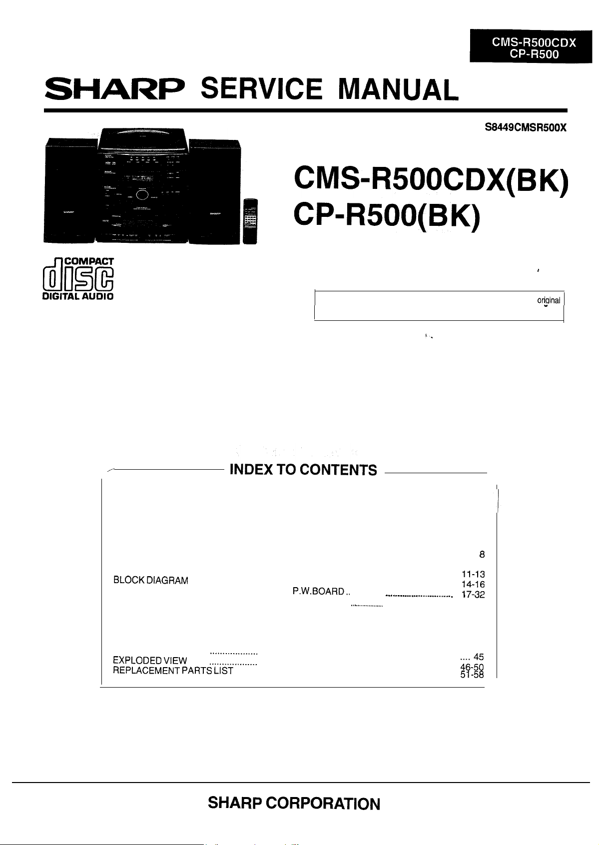
Page 1
SPECIFICATIONS
VOLTAGE
AC POWER SUPLLY CORD AND PLUG
NAMES
OPERATION
DISASSEMBLY
REMOVING AND REINSTALLING THE MAIN PARTS
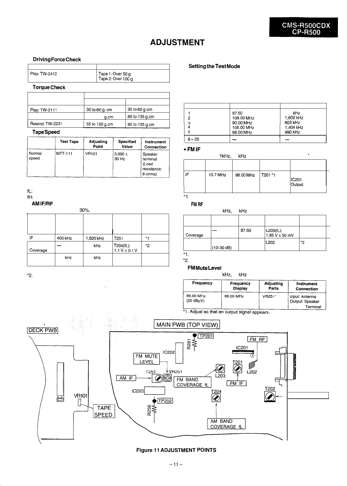
ADJUSTMENT
SCHEMATIC
WAVEFORMS OF CD CIRCUIT..
TYPES
NOTES ON
TROUBLESHOOTING
FUNCTION TABLE OF IC .
LCD SEGMENT
SELECTION
OF PARTS
OF TRANSISTOR
....
..............................................................................................................
.............
.............................
MANUAL
.............................................................................
DIAGRAM /WIRING SIDE OF
SCHEMATIC DIAGRAM
...............
......................
...................
(CD
............
........
LlST
.............................................................................................
.................
................................................................................
............................................................................................
.............................................................................................
..............................................................................
. . . . . . . . . .
..............................................................................
.............................
............................
SECTION)
.............................................................................................
.......................
............................................
.
. . .
.
.
. . . . .....
.......
. . . . . . . . . . . . . . . . . . . .
l
In the interests of user-safety the set should be restored to its
condition and only parts identical to those specified be used.
Page
2
3-5
7,
9,
10
33
34
34
35-39
40-44
2
2
6
..............................................................
..............
.
. . . . . ..-................. . . . . . . . . . . . . . . . . . . . . . . . . . . . . .
........................................................................
............................................................
......................................................................................................................
.
. .
.....
. ............................................................
...............................
Page 2
FOR A COMPLETE DESCRIPTION OF THE OPERATION OF THIS UNIT, PLEASE REFER
TO THE OPERATION MANUAL.
n
Compact disc stereo music system
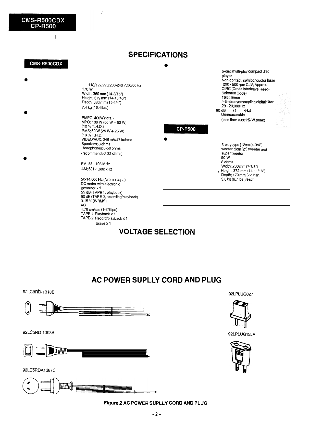
General
Power source:
Power consumption:
Diemensions:
Weight:
Amplifier section
Output power:
Input terminal:
Output terminals:
Tuner section
Frequency range:
l
Cassette deck section
Frequency response:
Motor:
Signal/noise ratio:
Wow and flutter:
Bias and erasure system:
Tape speed:
Heads:
AC 27/220/230-240
(15-l/4”)
531-l
Record/playback
MHz
playback)
Compact disc player section
Type:
Signal readout:
Rotational speed:
Error correction:
Quantization:
Filter:
Frequency response:
Dynamic range:
Wow and flutter:
Speaker system
Type:
Maximum input power:
Impedance:
Dimensions:
Weight:
20,000
Height;
type
Approx.
Wpeak)
tweeter
(7-l/16”)
filter
Specifications for this model are subject to change without prior
notice.
The voltage selector is located on the AC voltage selector box.
If adjustment is necessary, use a screwdriver in order to turn the
selector in either direction until the correct voltage figure is
displayed in the window next to the adjustment screw.
Page 3
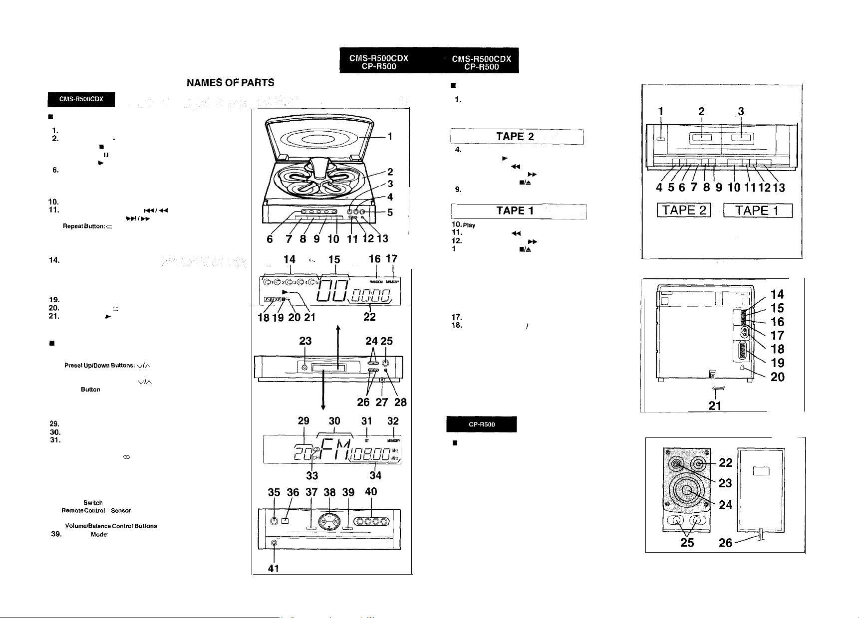
5-disc multi-play
Dust Cover
Disc Tray (Disc 1 - 5)
3.
Stop
4.
Pause Button:
5. Play Button:
Disc Number Select Buttons
7. Disc Skip Button
8.
Clear Button
9. Memory Button
Random Button
Track Down/Review Button:
12. Track Up/Cue Button:
13.
Disc Number Indicator
15.
Track Number indicator
16.
Random Indicator
17.
Memory Indicator
18. Extra Bass Indicator: X-SASS
Pause Indicator: II
Repeat Indicator:
Play Indicator:
22. Minutes and Seconds Indicator
compact disc player section
Button:
I
Stereo synthesizer tuner section
23. Stand-By Indicator
24.
25.
Band Selector Button
26. Tuning Up/Down Buttons:
27. Reset
28. Memory Button
/
Stereo double cassette deck section
Dubbing Speed Switch
2. TAPE 2) Cassette Compartment
3. TAPE 1) Cassette Compartment
Record Button:
5. Play Button:
6.
Rewind Button:
7. Fast Forward Button:
8. Stop/Eject Button:
Pause Button: II
Button: .
Rewind Button:
Fast Forward Button:
3. Stop/Eject Button:
n
Rear panel
14. FM 300 ohms Aerial Terminal
16. FM 75 ohms/ FM 300 ohms Aerial Terminal
16. FM/AM Aerial Earth Terminal
AM Aerial Terminal
Video (Audio Signal) / Auxiliary Input Sockets
18. Speaker Terminals
20. AC Voltage Selector
21.
AC Power Lead
l
Bend Indicator
FM Stereo Mode Indicator
32.
33. FM Stereo Indicator:
34.
n
35.
36.
37. Extra
38.
40. Function Selector Buttons
41. Headphones Socket
Indicator
Memory
Frequency
Station
Integrated stereo amplifier section
Power
Bass Button : X-BASS
Equalizer Mode Button
-3-
Speaker section
22. Tweeter
23.
Super Tweeter
24. Woofer
25.
Bass Reflex Ducts
26.
Speaker wire
-4-
Page 4
n
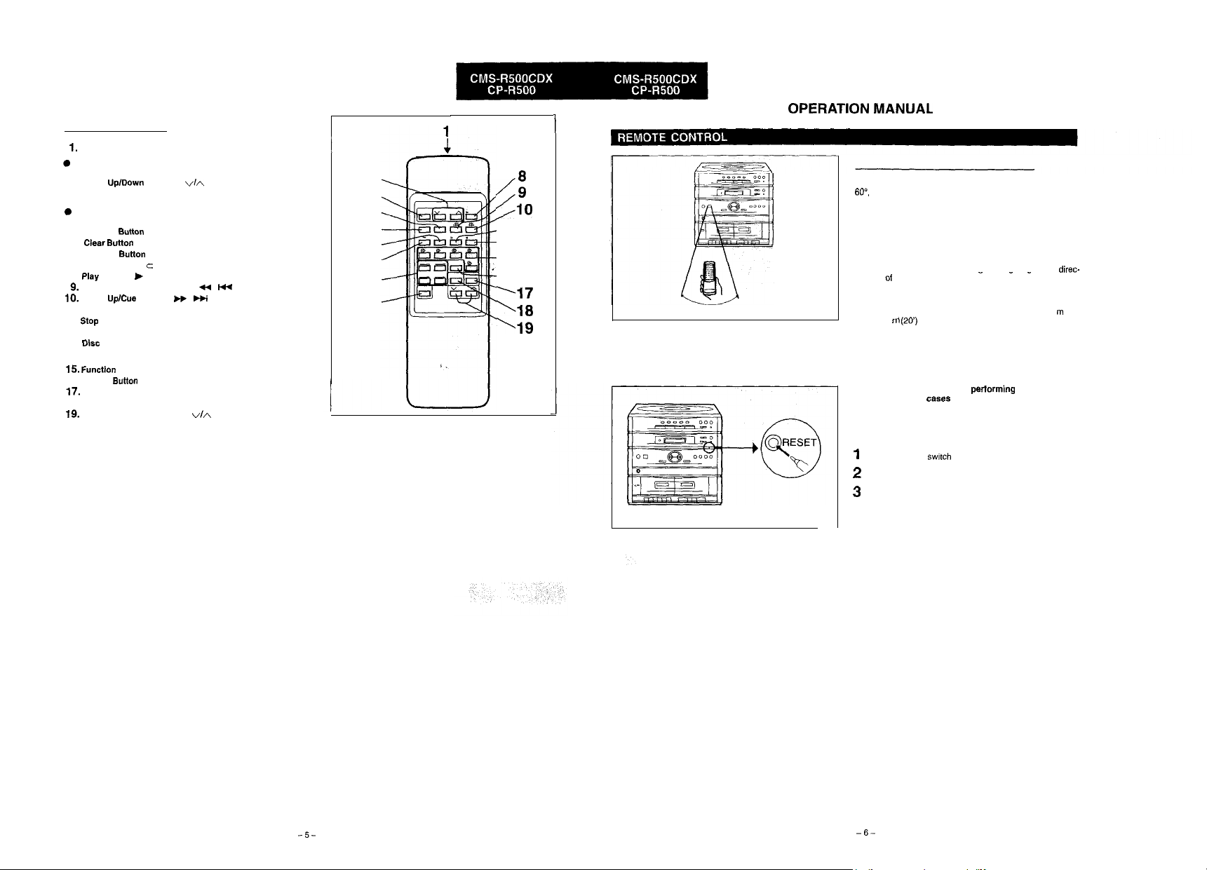
Names of controls
MANUAL
Remote Control Transmitter Window
Tuner control buttons
2. Preset
3. Band Selector Button
Buttons:
CD control buttons
4. Memory
5.
6.
Random
7. Repeat Button:
8.
Track Down/Review Button:
Track
Il.
Pause Button: II
12.
13.
Disc Number Select Buttons
14.
16. Power
Equalizer Mode Button
18.
Extra Bees Button : X-BASS
Volume Up/Down Buttons:
Button:
Button:
n
Skip Button
Selector Buttons
I
n
Proper use of the remote control
2
3
4
5
6
7
I
15
16
r-11
-12
-13
-14
60”
Aim the remote control at the remote control sensor within
with no obstacles, and operate es shown.
Notes concerning use:
l
Replace the batteries if control distance decreases or
operation becomes erratic.
l
Periodically clean the transmitter window on the remote
control and the sensor on the main unit with a soft cloth.
l
Exposing the sensor on the main unit to strong light can
interfere with operation. Chanae the liahtina or the
tion
the unit:
l
Keep the remote control away from moisture, excessive
heat, shock, and vibrations.
l
The remote control’s usable range is between 0.2
and 6 away from the sensor.
Reset the microcomputer by pertorming the following
procedure for the cesee shown below:
l
To erase all of the stored memory contents, or
l
If the display does not function properly, or
l
The unit does not operate properly.
Disconnect the AC power lead from the AC socket.
Press the RESET button for at least 3 seconds.
(8”)
to STAND-BY.
Page 5
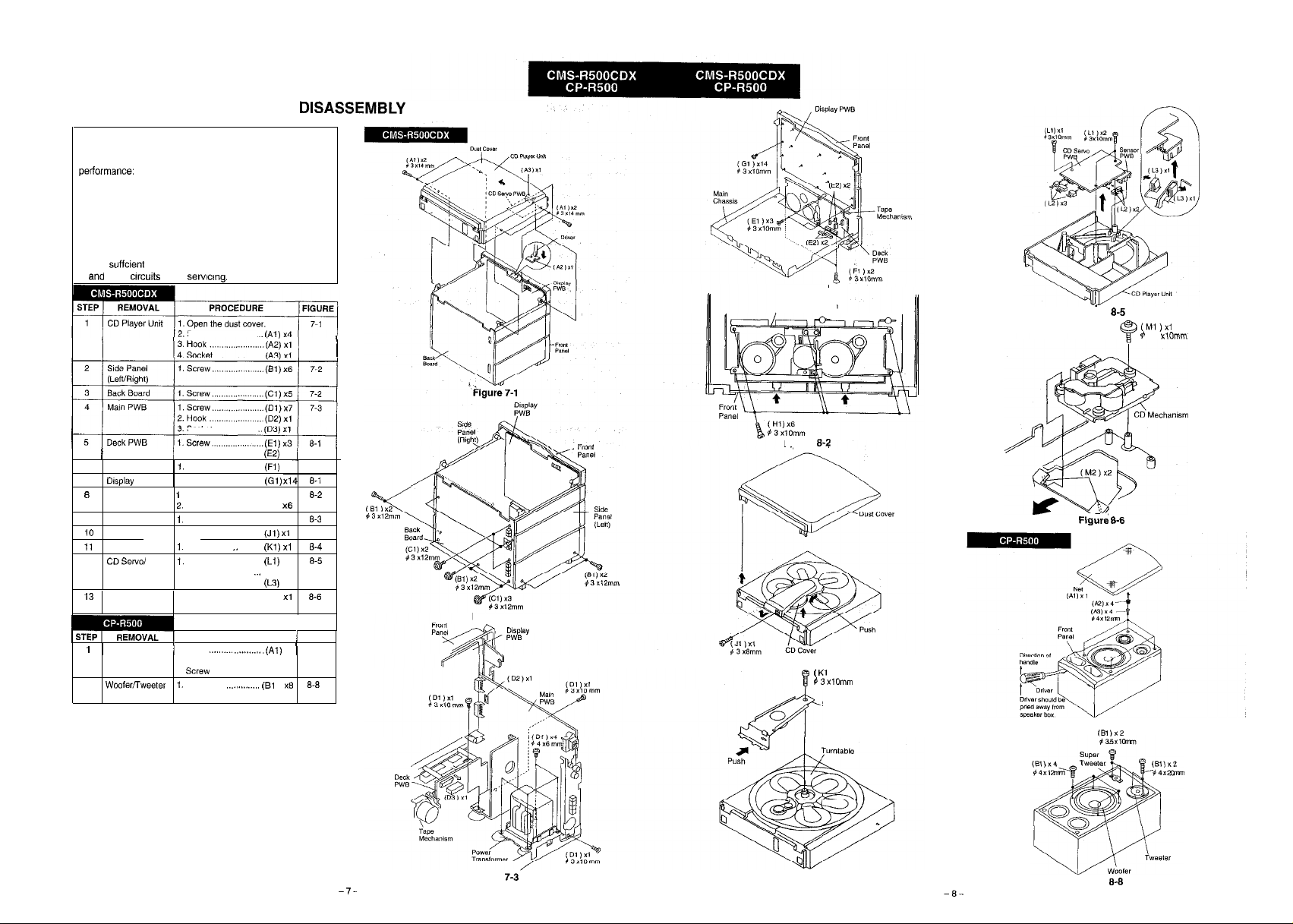
Caution on Disassembly
Follow the below-mentioned notes when disassembling the
unit and reassembling it, to keep its safety and excellent
1. Take cassette tape and compact disc out of the unit.
2. Be sure to remove the power supply plug from the wall outlet
before starting to disassemble the unit.
3. Take off nylon bands or wire holders where they need be
removed when disassembling the unit. After servicing the
unit, be sure to rearrange the leads where they were before
disassembling.
4. Take suffcient cars on static electricity of integrated circuits
other
when servcmg.
Screw
Figure 8-l
, Tape Mechanism
Figure 8-5
2.6
Socket
2. Socket..
6
Front Panel
7 Display
PWB
Tape Mechanism
9
Dust Cover
CD Cover
Turntable
12
Sensor PWB2.Socket..
CD Mechanism1.Screw
Front Panel
2
Super Tweeter
Screw..
1. Screw..
Open the cassette holder.
Screw..
See Rg.8.3.
1.
Screw..
Screw..
screw..
3 Hook
2. Hook
1. Net
2. Holder
3.
Screw
................... (EZ)
...................
........ ...........
................. (HI)
......... ..........
.....
.........
...................
...
....
.....
............... .......
(MP)
PROCEDURE
(A2) x4
x4
x2
x3 8-5
(L2) x5
x2
(Ml) xl
.(Al) xl
(A3) x4
)
x2
FIGURE
6-l
8-3
a-7
Figure 7-2
Figure 8-2
Figure 8-3
) xl
Stabilizer Bracket
Figure 6-7
Figure
Figure 6-4
Figure 6-6
Page 6
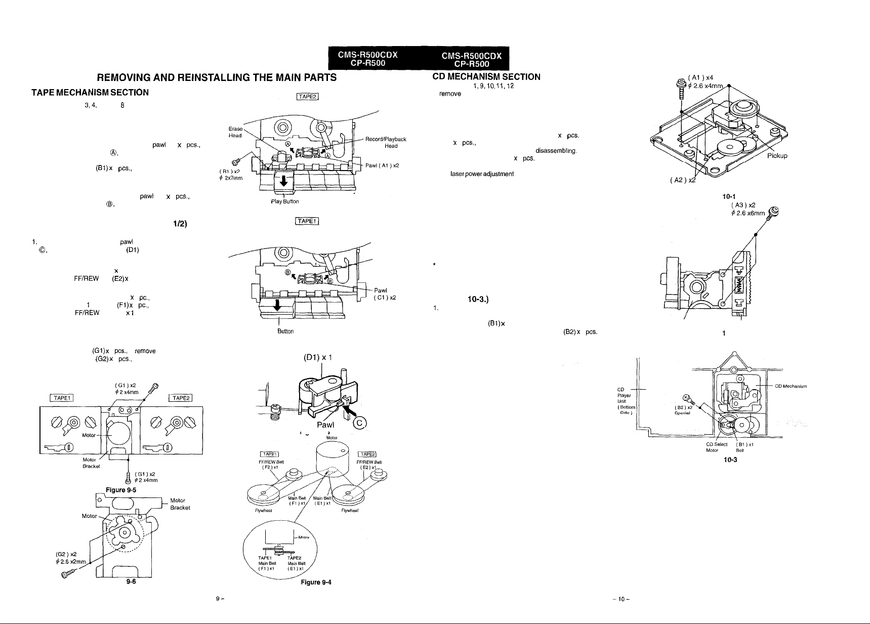
Perform steps 1, 2,
remove the tape mechanism.
5, 6 and 8 of the disassembly method to
How to remove the record/playback and erase
heads (TAPE 2) (See Fig. 9-l.)
1. Carefully band the record/playback head
the direction of the arrow
head upwards.
2. Remove the screws 2
and remove the record/playback
to remove the erase head.
(Al)
2
in
How to remove the playback head (TAPE 1)
(See Fig. 9-2.)
1. Carefully band the playback head
direction of the arrow
upwards.
and remove the playback head
(Cl)
2
in the
How to remove the pinch roller (TAPE
(See Fig. 9-3.)
Carefully bend the pinch roller
and remove the pinch roller
in the direction of the arrow
upwards.
How to remove the belt (TAPE 2) (See Fig. 9-4.)
1. Remove the main belt (El)
2. Remove the FF/REW belt (E2)
1 pc., from the motor side.
1 pc.
How to remove the belt (TAPE 1) (See Fig. 9-4.)
1. Remove the tape 2 main belt (El)
2. Remove the tape
3. Remove the FF/REW belt (F2) pc.
main belt 1
1
from the motor side.
from the motor side.
How to remove the motor
(See Figs. 9-5 and 9-6.)
1. Remove the belt.
2. Remove the screws 4
3. Remove the screws (G2)
Note:
When mounting the motor, pay attention to the motor mounting
angle.
to remova the motor bracket.
2
to remove the motor.
69
Play
Figure 9-l
Figure 9-2
Pinch Roller
Playback Head
Perform steps
to remove the CD mechanism.
and 13 of the disassembly method
How to remove the pickup
(See Figs. 10-l and 10-2.)
1. After removing the CD mechanism according to the disassembling procedure, remove the screws, (Al)
(A2)
2
2. Fit a new pickup in reverse order of disassemblrng. After fitting,
lock it with the screw (A3)
3. Connect the connector and lead wire as it was.
4. The
ment of performance of pickup.
Note:
When replacing the pickup do not apply force to the turntable of
spin motor. Otherwise, the height of main chassis and turntable
may be varied.
and replace the pickup.
2
is not necessary owing to improve-
4
and shafts
After replacing the pickup
This new mechanism has been newly designed to enhance
remarkably its performance as compared to the former ones, so
that there is no need to adjust pickup posture,
After mounting the pickup, apply voltage to the slide motor, and
ascertain that it runs at DC 1.5 V or less.
How to remove the the CD select motor
(See Fig. 10-3.)
Refer to “Removing the turntable and remove the turntable”
(See Figs. 8-3, 8-4 and 8-5)
2. Remove the belt 1 pc.
3. Remove the select motor mounting screws 2
Shaft
Pickup
Fiaure IO-1
Rack Gear
Figure
O-2
Figure
Fiaure 9-3
Figure 10-3
Page 7
MECHANISM SECTION
l
Torque Meter
l
Torque Meter
Fast forward: TW-2231
l
55to120
Tape 1
Specified Value
Over
Over
Specified Value
Tape
l
Keeping the TUNING (DOWN) button and MEMORY button pressed,
turn on POWER. Then the frequency is initially set in the memory as
shown in Table. Call with the PRESET button to use itforadjustment and
check of tuner circuit.
2
Preset No.
FM
MHz
MHz
MHz
Signal generator:
Test
Stage Display
Frequency
MHz
40 kHz dev., FM modulated
Frequency Adjusting
MHz
Parts
AM
531
Instrument
Connection
Input: Pin 1 of
TUNER SECTION
Low-range frequency
High-range frequency
l
IF/RF
Signal generator: 400 Hz,
Test
Stage
Band
Tracking
l
1 Input: Antenna terminal
Input: Input is not connected.
Frequency
990
AM modulated
Frequency Specified
Display Value/
Adjusting
Point
531
990
T202
Output: Speaker terminal
Output: TP201
Instrument
Connection
l 1
Adjust the T201 so that an-output signal become maximum.
l
Signal generator: 1
Test Stage Frequency
Band
RF
96.00 MHz
Input: Input is not connected.
Input: Antenna
l
Mute
Signal generator: 1
40
dev., FM modulated
Frequency
Display
MHz
98.00 MHz
40
dev., FM modulated
Serringl
Adjusting Point Connection
Output: TP201
Output: Speaker terminal
Speaker
terminal
instrument
‘1
ANTENNA
TERMINAL
AM TRACKING
Page 8
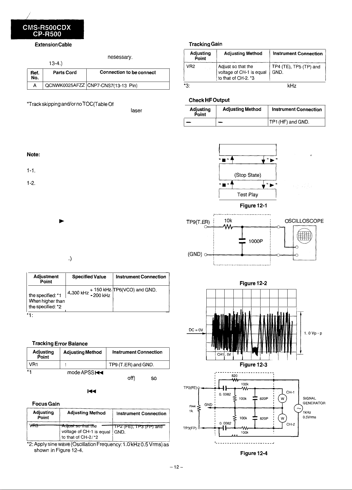
n
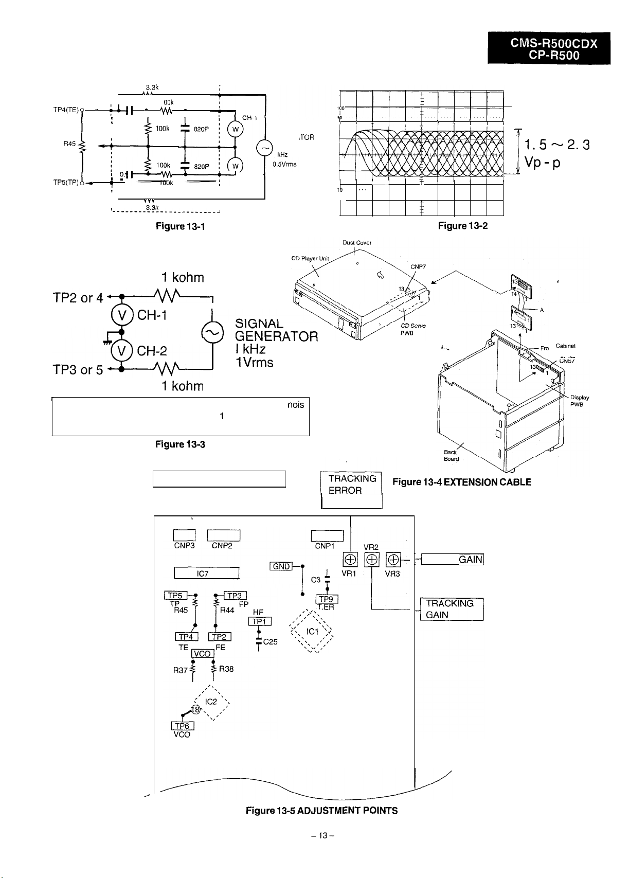
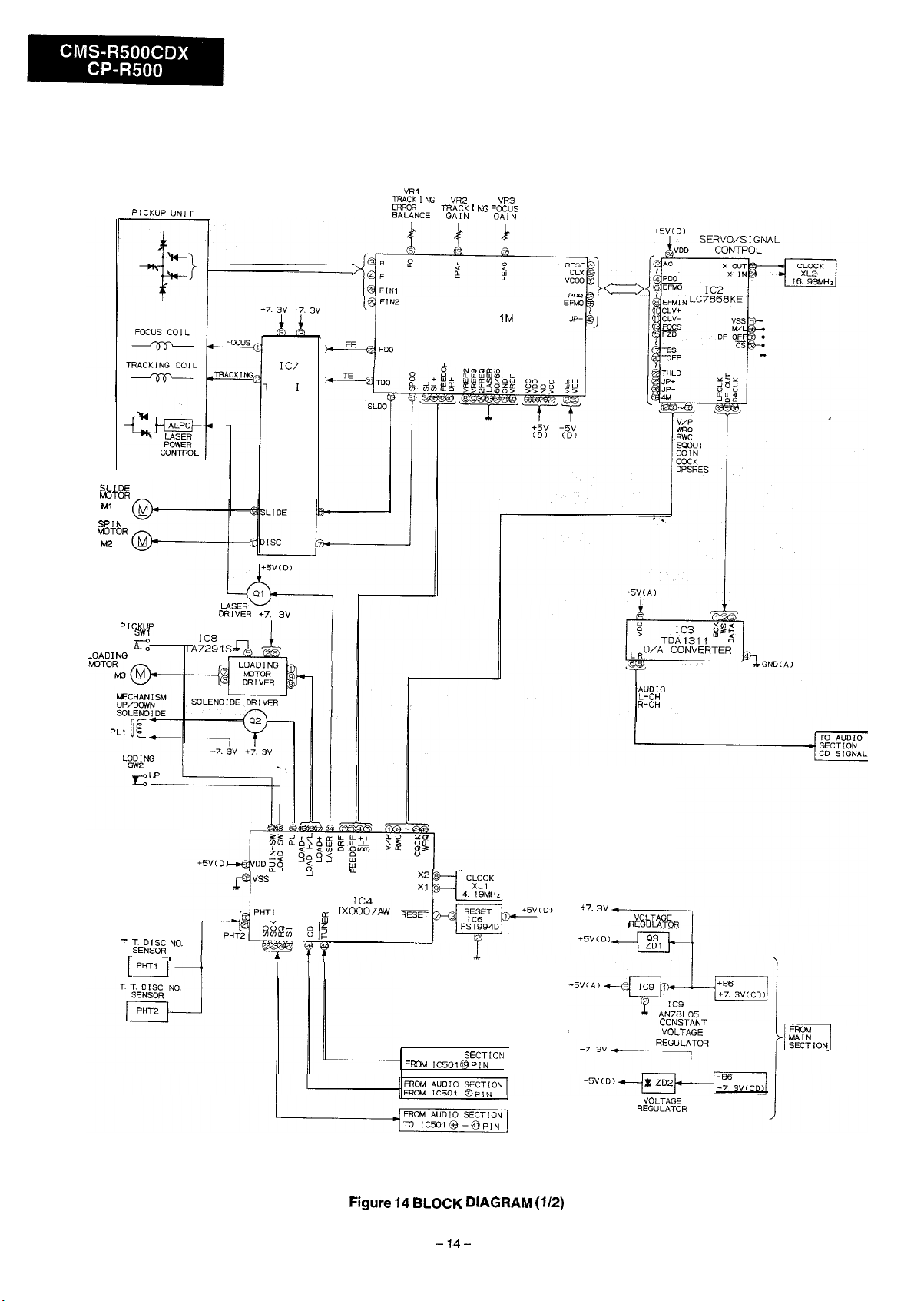
When performing adjustment or operation checks, use the extension cables as showm below, when nesessary.
(See Fig.
l
CD SECTION
Contents) maybecaused
by a build up of dust other foreign matter on the
pickup lens.
Before attempting any adjustment make certain that the lens is
clean. If not, clean it as mentioned below.”
1. Turn the power off.
2. Gently clean the lens with a lens cleaning tissue and a small
amount of isopropyl alcohol.
Do not touch the lens with the bare hand.
1. Preparation for Adjustment
Remove the CD section from the main unit, and connect the
CD section to the main unit using a jig cable unit.
Test mode setting
With the PAUSE II button and STOP n button pressed, turn
on the power switch.
l-3. Test mode operation
When the test mode is entered, the CD mechanism will move
down.
When the
button is pressed once, the CD mechanism will
move up.
When it is pressed again, the CD mechanism will play. When
the n button is pressed during play, the CD mechanism will
stop.
When it is pressed again, the CD mechanism will move down.
(See Fig. 12-l
2. VCO Free-Run Frequency
When lower than
*I
Cut the R37 (39 kohms).
‘2: Cut the R38 (33 kohms).
3. Servo Unit
Follow the procedure stated below.
l
: When the play modeAPSS
of tracking error balance. (Tracking server
obtain symmetric waveform (Figure 12-3.) when DC is 0 V.
After adjustment APSS
(Tracking servo ON)
l
l
button is pressed, adjustment
Adjust
as to
button is pressed.
Apply sine wave (Oscillation Frequency: 1 .O kHz 0.5 Vrms) as
shown in Figure 13-I.
l
Make sure that waveform is as shown in Figure 13-2.
Test Mode Start
CD Mechanism Down
CD Mechniam Up
12-l
TRACKING ERROR
BALANCE ADJ. JIG
More than
wave (Oscillation
820
FOCUS GAIN ADJ. JIG
Page 9
-
0.0082
GND
lk
I
TRAC
KING GAIN ADJ. JIG
1
SIGNAL
GENERP
1 kHz
CH-2
I
The jig (BPF) are recommended to reduce high frequency nois
during alignment. As an alternative, two
be used to achieve the same results.
kohm resistors can
0%
nt
CD SERVO PWB (TOP VIEW)
BARANCE
I
FOCUS
Page 10
LASER
POWER
CONTROL
IN
LA6524
-RACK
/FOCUS
DR I VER
NC
FOCUS
ICI
LA921
SERVO AMP.
NG
CD CONTROL
MICROCOMPUTER
FRW AUDIO
SECTION
Page 11
Page 12
Page 13

Page 14

Page 15

1
2
3
I
-23-
4
5
6
Figure 23 WIRING SIDE OF P.W.BOARD (2/3)
7
9
10
11
12
Page 16

Page 17

Page 18

A
C
E
F
G
L
. NOTES ON SCHEMATIC DIAGRAM can be found on page 34.
1
2
Figure
29 SCHEMATIC
I-
DIAGRAM
I NVERTER
9
11
12
Page 19

Page 20

HF
0
FRF
FE
0.
STOP-PLAYBACK
PLAYBACK
l
Resistor.
To differentiate the units of resistors, such symbol as K and M
are used: the symbol K means 1000 ohm and the symbol M
means 1000 kohm and the resistor without any symbol is ohm-
type resistor.
l
Capacitor:
To indicate the
P means micro-micro-farad and the unit of the capacitor without
such a symbol is microfarad. As to electrolytic capacitor, the
expression “capacitance/withstand voltage” is used.
STOP-PLAYBACK
DATA
0
(ML): Mylar type
l
Schematicdiagram and Wiring
are subject to change for improvement without prior notice.
REF. NO
SW2
SW101
SW401
SW501
CD-MEMORY
the one with “Fusible” is a fuse type.
of capacitor, a symbol P is used: this symbol
Temperature compensation
DESCRIPTION
L
RECORD/PLAYBACK
DUBBING SPEED
POSITION
OFF
OFF
PLAYBACK
OFF
OFF
OFF
OFF
OFF
OFF
OFF 1
DIAGRAM
The indicated voltage in each section is the one measured by
Digital Multimeter between such a section and the chaws with
no signal given.
In the tuner section,
indicates AM and
in the FM ST mode.
2. In the main section, a tape is being played back.
3. In the deck section, a tape is being played back.
indicates the record state.
4. In the power section, a tape is being
5. In the CD
indicates CD playback.
l
Parts marked with
thesafetyoftheset. Besureto replacetheseparts withspecified
ones for
the CD is stopped.
the safety and performance of the set.
FM MONO
played
back.
are important for maintaining
FRF
FOCUS COIL
0.
PLAYBACK
(DC)
-33-
BAND
SW517
SW518
SW520 CD
PRESET DOWN
PRESET UP
RN1202
OFF
OFF
OFF
OFF
L
GR RN1207
K
RN2202
C
RN2204
GR
Figure 34 TYPES OF TRANSISTOR
I
SR
BCE
Page 21

When the CD section dose not operate When the objective lens of the optical pickup is dirty, this section may not operate. Clean the
objective lens, and check the playback operation. When this section does not operate even
items. Remove the cabinet and follow the troubleshooting instructions.
“Track skipping
Before attempting any adjustment make certain that the lens is clean. If not, clean it as mentioned below.”
Turn the power off.
2. Gently clean the lens with a lens cleaning tissue and a small amount of isopropyl alcohol.
Do not touch the lens with the bare hand.
Turn the power switch on the unit to ON.
no TOC(Table Of Conetents) may
above step is taken, check the following
by a build up of dust other foreign matter on the laser pickup lens.
When the CD mode is entered, does the LCD change from
displaying “CD” to the function display “01 O:OO”?
Does the CD mechanism move down? Does the turntable
rotate?
Does the spin motor run?
When the disc is initialized, is TOC read?
Is TOC set to the playback mode?
Is there any audio
output
Check the item of “The CD microcomputer circuit
No
No
No
No
No
No
ates improperly”.
. . Check the item of “The CD mechanism moves up or down
improperly”.
Check the item of “The turntable operates improperly”.
Check the item of “The mechanism up operation is not
being detected”.
Check the item of ‘The spin motor does not run.”
Check the item of “The disc does not playback.”
Check the audio circuit.
OK
Page 22

l
Turn the power switch to ON.
Check the power circuit voltage.
Is the oscillating circuit
operating normally?
Check to see that the reset circuit of the control microcomputer
(lC4) is operating normally.
Is the drive signal of the LCD
Are the connector and PWB pattern damaged?
Is one of the motor drive output pins 15and 17of microcomputer
held “I-“?
of the control microcomputer (IC4)
Normal
being
output from the
Yes
Normal
OK
odown4mpreperly.
1
Defective replace faulty parts.
control
Check the XL1 and peripheral circuits and replace faulty
No
parts.
Check the reset circuit (IC6) and peripheral circuits and
The microcomputer (IC4) is defective. Replace it.
The microcomputer (IC4) is defective. Replace.
Is there any output between
the loading motor rotating?
Belt slip: Clean the pulley belt.
Replace the belt.
Are the plunger suction output pin 55 of microcomputer (IC4)
held “L”?
Is +B(7.5
The plunger and suction mechanism are defective.
Replace the plunger or the drive mechanism.
being output to pin
Yes
The motor drive
The loading motor (M3) is defective. Replace.
The turntable shutter, sensor
No
No
(PHT
The microcomputer (IC4) is defective. Replace.
The plunger driver circuits (Q2) are defective. Replace.
are defective. Replace.
input terminal state of
microcomputer
(IC8) is defective. Replace.
and sensors
1 2 3 4
Pin 21
Pin 22 H L H
H H L H H
H L
Page 23

l
Has the mechanism up detection input pin 18 of
microcomputer (IC4) changed to
Has the motor drive output of microcomputer (IC4) been turned
OFF (pins 15 and 17: “H”)?
Yes
The motor drive
motor M2 is defective. Replace it.
is defective. Replace’.
The mechanism up switch or detection mechanism is
No
defective. Replace.
The microcomputer (IC4) is defective. Replace.
is defective. Replace it.
is defective. Replace it.
is defective. Replate it.
l
Is the disc initialized? Does the laser diode go on?
Does the tracking servo operate normally?
Is the EFM signal of pin 72 of ICI flat? (Lower side)
Is the tracking error signal (
Yes
Yes
Normal
A: Check the item of “The laser diode goes on.”
B: Check the item of “The laser diode does not go on.”
Check if the objective lens of the
No
No
pickup is dirty.
If it is dirty, clean it.
Does the spin motor run normally? Check the waveform of
pins 10
Is there any dropout part in the EFM signal of pin 72 of ICI?
Replace the disc or change the program.
Is the tracking signal being out-
put from the pickup main unit?
and 11 (CLV-) of
Normal
Yes
IC2 is defective.
No
Replace it.
The pickup is
defective.
Yes
Is the tracking coil drive output being output from the tracking -- IC7 is defective.
driver output (pin 2 of
Yes
The pickup connecting connector is broken.
The pickup tracking coil is broken.
No
The PWB negative pattern is damaged.
Replace the
Page 24

When the CD Mecahnism moves up without loading disc, does the pickup lens move
up and down?
the EFM signal of pin 72 of
being output?
No
l
Pickup height error
l
Laser diode output error
NO
Are the voltages at pins 8 and 3 of the focus
driver (IC7) +7.5V and -7.5V, respectively?
Yes
Is the high/low level repetition output for
leading the focus servo of pin 13 of
being output?
Yes
of
Is the DRF disc
reflection
signal
pin 40 of the servo signal control
at a high level?
Yes
shown below?
Pin 40
DRF
Pin 26
FEAO
The servo amplifier
The servo amplifier
) is defective.
is defective.
is defective.
Is the high/low repetition output being
output from pin 22 of
The focus error
Replace it.
Yes
Is the high/low repetition output being
output from pin 1 of
Check connectors
and
is defective.
Yes
Check to see that the focus circuit is normal and check the
distribution connector.
The focus driver (IC7) is defective. Replace it.
Page 25

(IC4) at a low level?
Yes
emitter voltage
Yes
The laser diode is defective.
Check the powercircuit.
No
Is the pickup returned to the innermost part?
Is the pickup in switch
Check if pins 4 (SLM+) and 5
Check pin 33 of servo A
Check pin 9 of the slide
Check if there is voltage at CNP3,
turned to ON?
No
and Ml.
Yes
Replace the pickup.
IS
pin
of
at a low
level?
Yes
IC4 is defective. Replace it.
IC4 is defective. Replace it.
The servo AMP.
The slide motor driver (IC7) is defective. Replace it.
is defective.
Replace it.
is defective. Replace it.
Is there audio output?
Is there audio output fro
Checking the D/A circuit.
Yes
I
l
No
Check sound coupling capacitors
(R-CH).
(L-CH) and C92
Page 26

Tuner/System Control
this
terminal
asterisk
terminal
Page 27

CLOCKED
I
Tuner/System Control
A
PROGRAM
ROM
PR
OGRAM
MEMORY
q
GENERAL
DATA
REG.
BITS
I I
CPU
CLOCK
Page 28

terminal
asterisk
terminal
Page 29

unit, the terminal with asterisk mark (*) is (open) terminal which is connected to the outside.
In this
CD Control Microcomputer
TIO
1
s
I NTTO
I NTERRUPT
CD Control Microcomputer
ROM
PROGRAM
MEMORY
2160X.3
TS
MEMORY
BITS
P73
I
CLOCK
OUTPUT
CONTROL
CLOCK
CLOCK STAND BY
GENERATOR
Xl x2
Page 30

OK
Page 31

Page 32

Page 33

Page 34

IC6
REPLACEMENT PARTS LIST
“HOW TO ORDER REPLACEMENT PARTS”
To have your order filled promptly and correctly, please furnish the following information.
NOTE:
Parts marked with “A” are Important for maintaining the safety of the set. Be sure to replace these parts
for maintaining the safety and performance of the set.
INTEGRATED CIRCUITS
J Servo Amp.,LA9211M
J CD Control Microcomputer,
J Reset.PST994D
J Tracking/Focus Driver,
J Loading Motor Driver,
J PLL.TC9216P
J FM IF
J Audio Processor,TDA7318
J
TRANSISTORS
J
J
J
J Stlicon,NPN,ZSC535 C AC
J Digital,PNP.RNZZOZ AB
J Sillcon,NPN,ZSC1740 SR
J
J
J Digital.PNP,RNZZOZ
J
J
J Silicon.NPN.ZSC1740 SR
J
Silican.NPN.‘ZSCZOOl L
J Silicon~NPN;ZSDZOlZ
Q251
Q604
Q658.659
Q660
RH-
RH-
1. MODEL NUMBER
3. PART NO.
PARTS-DELIVERY SECTION
Control,
LA6524
Playback Amp.,AN7345K
AM IF,LA1832
Control,
GR AB
CODE
AQ
AN
AY
AC
AH
AG
AE
AM
AG
AL
AR
AX
AY
AB
AB
AC
AD
AB
A0
AD
2. REF. NO.
4. DESCRIPTION
Q661
Q664
Q667
Q669
D5
LED501
VD202
ZD653
ZD655.656
CF251
T204
T251
J
TRANSFORMERS
DESCRIPTION
J
J Sflicon,NPN,2SD2012
J Silicon,PNP,ZSBL375
J
J
J
DIODES
J
J Sllicon,RL104AT
J
J
J
J
J
J
J
J
J
Variable Capacitance,
Variable Capacitance.
J Zener.6.2V.MTZJ6.2C
FILTERS
J FM Detector
J FM IF
J AM IF
J Power
specified ones
GR
CODE
A6
AD
AF
A8
A8
AB
AB
AA
AA
AB
AC
AD
AA
AA
AA
AA
AA
AA
AG
AA
AE
AE
AS
AC
AC
AA
AB
AC
AA
AD
AH
AD
AD
AC
AF
VA2
VR251
x251
x252
XL1
XL2
XL501
There are two types of capacitors
other by reading their Part Numbers.
The capacitance error of each capacitor is indicated by the symbol given at
13th digit of the Part Number
(Tubular type ceramic capacltar is
(Tubular type
NO.
c3 VCTY,#,lCX472K J 0.0047 pF,16V AA
c4
C6
c7
L6
Ceramic
A symbol “c”
. Semiconductor type capacitor:
A symbol “T”
NO.
VP-CH27QKQQQQ J 27
VARIABLE RESISTORS
capacitor;
“K” is given at the 3rd digit of its Part Number like “VCC
gwen at the 3rd diglt of its Part Number
capacitor is identified by the symbol MF(MN)
otherwise specified,
this MF(MN)
COILS
J 2.2
J 27
J 1.8 mH.Choke
J
mH,Choke
J 330
J FM Oscillation
J 100
J
mH,Choke
J 100 ,zH,Choke
J 2.2
J
[Tracking Error
J 5 kohms
[Tracking Gain1
J
kohm
[Focus Gain1
J
VIBRATORS
CAPACITORS
“D”
this TV(TQ/CY) does not mean the lead
J 33
J 47
Speed1
kohm
Mute Level1
Crystal,456
MHz
and they can be identified from
not mean the lead wire)
capacitors are
sF,SOV.Electroiytic
“z”
by the symbol TV(TQ/CY)
“M”
type.Q260
AB
A0
AC
AB
AB
AF
AA
AD
AB
AB
AB
A0
AB
AB
AB
AD
AK
AD
AG
AD
the par
AA
AA
AA
AA
AB
AB
AB
AB
AA
AA
AB
AA
AA
AA
AA
AA
AA
AB
AB
AB
A0
AA
AA
AA
AA
AA
AB
AA
AA
AB
AA
AB
AA
AB
AB
AB
AB
AA
AA
AA
AA
AA
AA
AB
AA
AB
AA
AA
AA
AA
AA
AA
AA
AA
AB
AA
A0
AA
AA
AB
AA
AB
AB
Cl6
C24
C25
C27
c31
C32
c34
c51
c52
C61
C65
C67
c71
c77
c79
c91.92
c93.94
Cl60
0.47 pF,SOV,Electrolytic
J 0.001 /1F,50”
J 0.022 #F,6.3V
J 220
J
J
J 47
J 0.022
J 470
J 0.001 pF,50V
J 220
J 330 pF,&3V,Electrolytic
J
J 330
J 560
flF.SOV,Ekctrolytic
J
J 0.01 pF.16V
J 0.001 fiF,SOV
J 0.0033 uF.16V
J
sF,StiV,Electrolytic
J 22 uF.16V.Electrolvtic
J O.O& pF.16V
J
220
J
33
J
470
J
47
J
0.0039 pF,lOOV.
Polypropylene
J
0.027 pF,SOV,Mylar
J
47 /rF,16V,Electrolytlc
J
2.2 flF,50V,Electrolytic
Page 35

Cl72
c212
C213
C214
C215
C216
C217
C218
C225
C226
C232
C234
C235
C236
C252
C256
C257
C258
c259
C261
C262
C263
C264
C265
C266
C275
C281
C282
C285
C286
C287
c292
c293
c294
c295
C296
C297
C298
c299
PART NO.
J
J 18 pF (CH),SOV
J
J
J
J
J
J
J
J
J
J
J
J
J
J
J
J
J 8.2 pF
J
J
J 18 pF (UJ),SOV
J 18 pF (CH),SOV
J
J
J
J
J
J
J
J
J
J
J
J
J
J
J
J
J
J
J
J
J
J
J 12 pF
J 15 pF
J
J
J
J
J
J
J
J
J
J
J
J
J
J
J
J
J
RC-GZA475AFlH
J
J
J
DESCRIPTION
J
0.022
22
0.01 /1F,16V
4.7
15 pF (CH),SOV
33
0.0047 ,~F,16v
10
0.001
0.022
0.001
0.022
10
0.022
100
8.2 pF (UJ),SOV
22
0.022
0.001
0.022
0.047 pF,5OV
0.022
470
0.022 ,uF,25V
0.022
10
0.022
22
0.001
2.2
1
0.022 ,uF,25V
120
0.022
3.3
0.022
22
0.001
1
1
0.015
22
0.1
0.022
0.01
330
0.022
0.022
47
0.001
0.33 ,uF,SOV,Electrolytic
47
0.022 /1F,25V
100
56
100
0.022
10
47
0.0018
4.7
0.22
100
CODE REF.NO.
AA
C421
AA
AA
AA
AA
AA
AA
AA
AA
AA
AA
AA
AB
C516
AA
AA
AA
AA
c529
AA
AA
AA
AA
AA
AA
AA
AA
AA
AA
AA
AB
AA
C631
AA
AA
C634
AB
C655
AB
AA
AA
AA
AB
C662
AA
C663
AB
C664
AB
C665
AA
AB
AB
AB
AB
AA
AA
AA
(Unless otherwise specfifed, resistors are
AA
AA
AA
AA
AA
AB
R3
AA
R4
AA
R5
AB
R6
AA
R7
AB
R8
AA
AB
AA
AB
AB
AA
R15
AB
R16
AB
R17
AA
PART NO.
1
100
J O.OOlpF,5OV
J 470
J 3.3
0.01
100
0.01
J
J 330
J
10
RC-GZA476AFlV J 47
10
100
J 2.2
100
10
10
RC-GZA336AFlC J 33
3300
1000
RESISTORS
J 0
J
1
J 15
J 56
J 8.2
120 kohms,l/8W
22 kohms,l/8W
680 ohms,l/8W
J 680
Ivory
DESCRIPTION
type.)
CODE
AB
AB
AB
AA
AA
AA
AA
AB
AA
AB
AA
AB
AA
AA
AA
AA
AA
AA
AA
AB
AB
AA
AA
AA
AB
AB
AB
AB
AB
AB
AB
AA
AA
AA
AB
AA
AA
AB
AB
AB
AB
AG
AD
AF
AF
AB
AA
AA
AA
AA
AA
AA
AA
AA
AA
AA
AA
AA
AA
AA
AA
AA
AA
AA
Page 36

REF.NO.
R22
R23
R24
R25
R26
R27
R28
R29
R30
R32
R33
R34
R35
R36
R37
R38
R39
R40
R42
R43
R48
R49
R50
R53
R54
R55
R56
R57
R63
R64
R69
R70
R71
R72
R73
R74
R75
R83
R84
R87
R95
R97
R120
PART NO.
VRD-MNZBDIOZJ
J
J
J
J
J
J
J
J
J
J
J
J
J
J
J
J
J
J
J
J
J
J
J
J
J
J
J 10
J
J
J
J
J
J
J
J
J
J
J
J
J
J
J
J
J
J
J
J
J
J
J
J
J
J
J
J
J
J
J
J
J
J
J
J
J
J
J
J
J
J
J
68
47
2.2
10
39
6.8
330
390
47
100
10
100
3.3
4.7
33
39
33
180
100
470
39
5.6
8.2
1
1
47
1.2
200
2.2
100
1
22
47
1
1.8
1.8
1.8
1.8
820
1.8
100
1.8
100
1.8
1.8
4.7
12
27
270
56
470
39
470
39
2.2
33
47
22
68
1
56
100
3.9
100
5.6
3.9
3.9
1
DESCRIPTION
CODE REF.NO.
AA
AA
AA
AA
AA
R133
AA
R134
AA
AA
AA
AA
R142
AA
R143
AA
AA
AA
AA
R153
AA
AA
R154
AA
R155
AA
R158
AA
R159
AA
R160
AA
AA
AA
R164
AA
AA
AA
AA
AA
R170
AA
R179
AA
AA
R201
AA
R202
AA
R203
AA
R204
AA
R205
AA
R206
AA
R207
AA
R208
AA
R209
AA
R210
AA
R219
AA
R220
AA
R223
AA
R224
AA
R251
AA
R252
AA
R253
AA
R254
AA
R255
AA
R256
AA
R258
AA
R259
AA
R260
AA
AA
AA
AA
R267
AA
R268
AA
AA
R279
AA
R280
AA
R281
AA
R282
AA
R283
AA
R284
AA
R285
AA
R286
AA
R293
AA
PART NO.
VRD-MNZBDIOZJ
3 J
J
6.8
J
560
J 100
J
10
J
680
J
470
J
3.3
J
27
J
10
J
4.7
J
10
J
10
J
4.7
J
10
J
27
J
100
J
47
J
22
J
22
J
68
J
6.8
J
2.7
J
1
J
4.7
J
4.7
J
10
J
33
J
1
J
5.6
J
10
J
10
J
22
J
100
J
33
J
10
J
47
J
680
J
270
J
1.2
J
4.7
J
100
J
4.7
J
68
J
100
J
6.8
J
2.7
J
270
J
10
J
3.3
J
3.3
J
6.8
J
1.8
J
4.7
J
27
J
3.3
J
10
J
1
J
33
J
1
J
2.2
J
2.7
J
10
J
150
J
5.6
J
12
J
10
J
47
J
390
J
5.6
DESCRIPTION
CODE
AA
AA
AA
AA
AA
AA
AA
AA
AA
AA
AA
AA
AA
AA
AA
AA
AA
AA
AA
AA
AA
AA
AA
AA
AA
AA
AA
AA
AA
AA
AA
AA
AA
AA
AA
AA
AA
AA
AA
AA
AA
AA
AA
AA
AA
AA
AA
AA
AA
AA
AA
AA
AA
AA
AA
AA
AA
AA
AA
AA
AA
AA
AA
AA
AA
AA
AA
AA
AA
AA
Page 37

REF.NO.
R295
R296
R297
R298
R417
R418
R451
R452
R523
R532
R533
R534
R537
R538
R539
R540
R541
R551
R613
R614 ,
R615
R616
R617
R620
R625
R626
R629
R630
R632
R639
R665
R668
R669
R670
R671
PART NO. *
J 5.6
J 470
J 560
J 820
J 5.6
J
J 100
J 1.2
J 5.6
J 2.7
J 47
J 1.2
J 1.2
J 8.2
J
JJ330
J 2.7
J 5.6
J 56
J 56
JJ560
J 560
J
J 150
J 220
J 39
J 220
J 3.3
1JJ
J
J 22
J
J
1
1
10
1
1
1
100
1
10
1
1
1
1
10
1
100
330
100
1
10
1
DESCRIPTION
CODE
AP
AP
AP
AP
AP
AP
AP
AP
AA
AP
AA
AA
AA
AA
AA
AA
AA
AA
AA
AA
AA
AA
AA
AA
AA
AA
AA
AA
AA
AA
AA
AA
AA
AA
AA
AA
AA
AA
AA
AA
AA
AA
AA
AA
AA
AA
AA
AA
AA
AA
AA
AA
AA
AA
AB
AA
AA
AA
AA
AA
AA
AA
AA
AA
AA
AB
AA
AA
AA
AA
REF.NO.
R691
R692
R693
CNP3
CNP4
CNP5
CNP7
CNP103
CNP104
CNS4
CNS7
CNS103
CNS104
LCD501
Ml
M2
M3
M601
RX501
so401
SO601
SW1
SW401
SW501
SW502
SW503
SW504
PART NO.
J
10
DESCRIPTION
J 68
OTHER CIRCUITRY PARTS
J Connector
J Plug,GPin
J
J
J
J
J
Part of
J
J
J
J
J
J Fuse,T3.15A L 250V
J Jack,Headphones
J Lamp
[Loading]
l/-l
J Receiver,Remote Control,
J
J
J
[Pickup In]
[Loading]
[Record/Playback]
[Dubbing Speed]
[Fast Forward]
[Rewind]
[Random]
L 250V
L 250V
L
Type
Type
Type
Type
Type
Type [Repeat]
Type
CODE
AA
AA
AA
AA
AA
AA
AA
AA
AF
AL
AD
AC
AB
AB
AA
AG
AB
AB
AB
AC
AC
AF
AL
AG
AD
AG
AF
AH
AD
AF
AF
AD
AD
AD
AD
AK
AV
AD
AP
AT
AS
AP
AM
AK
AK
AF
AG
AC
AC
AG
AF
AC
AC
AC
AC
Page 38

SW505
SW508
PART NO.
DESCRIPTION
Type [Play]
Type
CODE
AC
AC
[CD-Memory]
SW509
AC
[Tuning Down]
SW510
Type
AC
[Tuning Up1
SW511
AC
[Tuning-Memory]
SW512
SW513
SW514
SW515
SW516
SW517
Type [Clear]
Type [Power]
Type
AC
AC
AC
AC
AC
AC
[Preset Down]
SW518
Type
AC
[Preset Up]
SW520
SW521
SW522
SW523
SW525
Type
Type [Tuner]
Type [Tape]
Type
AC
AC
AC
AC
AC
[Balance-Left]
SW526
Type
AC
[Balance-Right]
SW527
Type
AC
[Disc Skip]
SW528
SW529
SW530
SW531
SW532
SW533
SW534
Type [Disc
Type [Disc
Type [Disc
AC
AC
AC
AC
AC
AC
AC
[Volume-Down]
SW535
Type
AC
[Equalizer Mode]
[Voltage
Type
Type
Selector]
Type
AC
AQ
SW536 AC
SW541
J
SW605 AE
[Tape 1 Main]
SW606 AE
Type
[Tape 2 Main]
SW607 AB
[Tape 1 Mute]
SW608
AB
[Tape 2 Mute]
DECK MECHANISM PARTS
1
2
3
4
5
6
10
12
13
14
15
J Joint
J Spring,Latch Plate AA
J Head,Erase
Plate
Lock
AC
AC
AB
AB
AB
AA
AA
AG
AA
AA
Lever
16
17
AA
AG
REF.NO.
18
19
20
21
22
23
24
25
26
27
28
29
30
31
32
33
34
35
36
37
38
40
41
42
43
45
46
47
48
50
51
52
53
54
55
56
58
63
64
66
67
68
69
70
71
72
501
503
504
505
506
508
509
510
511
SW605
SW606
SW607
SW608
301
PART NO.
J
J idler Lever Ass’y
J Lever,Main Lock
J Lever,AS Killer
J
J Lever,Record
J Lever,P-Kick
J
J Spring,Operate Lever
J Spring,Pause Killer
J Take-up Reel Ass’y
PCUSZO 162AFZZ
J Prevent Vibration Rubber
LX-WZ9064AFZZ J
J
J
LX-WZ9063AFZZ J
J
J Screw,dZmn P-Kick Lever
J Motor with Pulley [Tape]
CD MECHANISM PARTS
J
DESCRIPTION
Joint
Lock
1
21
Lever
Killer Lever
Stop Lever
[Tape
11
J Screw+$ZX4mm
J
J Screw,dZXSmm
Type
[Tape
Main]
[Tape 2 Main]
[Tape 1 Mute]
[Tape 2 Mute]
11
46XO.5mm
CODE
AG
AG
AA
AC
AB
AB
AC
AA
AB
AA
AB
AB
AA
AA
AB
AB
AB
AB
AB
AB
AF
AG
AA
AA
AC
AE
AB
AM
AD
AA
AA
AA
AA
AA
AA
AG
AA
AA
AA
AA
AA
AA
AA
AA
AA
AK
AA
AB
AA
AA
AA
AA
AA
AA
AA
AP
AE
AE
AB
AB
AA
Page 39

302
303
304
305
306
308
701
702
703
M2
201
202
203
204
205
206
207
208
209
210
211
212
213
214
215
217
218
220
221
222
8223
8223
8223
224
225
226
227
228
229
230
231
232
233
234
235
236
237
REF.NO.
1
2
3
1
2
1
2
PART NO.
CABINET PARTS
DESCRIPTION
J
J
J Gear,Rack,Fix
J
J
J Cushion
J Pickup Unit
J Screw,dPX3mm
J Screw,+2.6XGmm
J Motor with Gear
J Motor with Chassis
Front Panel
(Not Replacement Item)
J
J
J
[Tape
11
Cassette Holder
(Not Replacement Item)
J
[Tape
J Cassette Holder Ass’y
Cassette Holder
(Not Replacement Item)
J
J Spring,Cassette Up.
J Damper
J Knob,CD
J Knob,CD Disc
J Knob,Tuner
J Knob,Power
J Knob,X-BASS
J
J
J
J Knob,Function
J
J Main Chassis
J Bracket,Main PWB
J
J
J
J AC Power Supply Cord
[For Taiwan]
[For Saudi Arabia]
J AC Power Supply Cord
[For Australia]
J Gear,Driving
J Cam,Driving Gear
J Gear,Driving Gear Cam
J
J
J Cushion,Arm
J
J
J
Turntable
[Tape 21
Cover
Player Base
Bottom
Lock
CODE
AC
AB
AB
AB
AC
AC
BF
AA
AA
AA
AP
AT
AY
AC
AH
AA
AL
AD
AL
AD
AA
AD
AC
AF
AC
AC
AC
AD
AD
AC
AD
AE
AT
AF
AA
AD
AM
AM
AP
AC
AF
AC
AC
AE
AB
AH
AB
AB
AC
AD
AC
AW
AF
REF.NO.
238
239
240
241
242
243
244
245
246
247
248
249
250
251
252
253
254
255
256
257
258
259
260
261
262
263
265
266
267
268
269
270
271
601
602
603
604
605
606
607
608
609
610
611
612
614
615
616
617
618
619
620
621
622
623
PART NO.
DESCRIPTION
CODE
1
(Not Replacement Item)
2
J
Holder
AA
AK
1
(Not Replacement Item)
2
3
J Cu.shion,Stabilizer AD
J Stabilizer AE
J
AC
AA
J Heat Sink
J
J LCD Sheet
J Back Board
J Side Panel
J
J Hinge Ass’y
AR
AE
AE
AK
AN
AG
AH
AW
1
Dust Cover
(Not Replacement Item)
2
Hing
JBTN-0008AWSA J
[Tape
[Tape 21
J
[Tape
Forward
AC
AC
AV
AB
AB
AB
AB
[Tape
JBTN-0012AWSA J
JBTN-0013AWSA J
JBTN-0014AWSA J
JBTN-0015AWSA J
JBTN-0016AWSA J
JBTN-0017AWSA J
J Lever,Record
[Tape
[Tape 21
[Tape 21
[Tape
[Tape
Forward
11
[Tape
AB
AB
AB
AB
AB
AB
AB
AB
Button
AB
J Fuse Holder
J Magnet
J Spring,Lock Lever
J Bushing,AC Power Supply
AA
AE
AB
AD
AD
Cord
J Bracket,Heat Sink
J Heat Sink
1
J
J
J
J
J
J
J
J
J
J Screw,+43X25mm
J Screw,d2.6mm
J Washer,d3mm
J Screw,d3X
J
AF
AC
AC
AA
AA
AA
AA
AA
AA
AA
AA
AA
AA
AA
AA
AA
AA
AA
AA
AA
AB
AA
AA
AA
AB
-57-
Page 40

624
PART NO.
DESCRIPTION
J
ACCESSORIES/PACKING PARTS
J Packing
J Packing Case
T i NSTOOO
J Operation Manual
[For Thailand
[Except for Thailand]
T
NSZ0049AWZZ
J Operation Manual
[For Russian Only1
J AM Loop Antenna
Accessories
Dust Cover
J Polyethylene Bag,
AC Plug Adaptor
[Except for Australia]
J FM Antenna
[For Australia Only]
[For Saudi Arabia]
J Adaptor,AC Plug
[Except for Saudi
Arabia]
J Remote Control
J Battery Lid,Remote
Control
CODE
AA
AS
AF
AP
AF
AK
AA
AB
AB
AA
AD
AB
AD
AG
AX
REF.NO.
707
708
709
710
711
712
PART NO.
PACKING PARTS
DESCRIPTION
J Speaker Cord
J
J
J
J
Non-Polar
J Woofer
J Packing
Bottom,Speaker
J Sheet,Speaker
J Polyethylene Bag,Speaker
CODE
AG
AA
AA
AC
AC
AB
AD
BA
AT
AF
AH
AD
AD
P.W.B. ASSEMBLY (Not Replacement Item)
J Main/Power
(Combined Ass’y)
PWB-B 32Ll%B1862DPLS J Display
[For Australia Only]
PWB-Cl9
J CD Servo/Sensor
[For Australia Only]
PWB-D
J CD Motor (PWB Only)
[For Australia Only]
PWB-E
OTHER SERVICE PART
A
J Extension Cable,
SPEAKER BOX PARTS
701 92LPFPAlR500
J Front Panel Ass’y AW
Front Panel
(Not Replacement Item)
2
702
1
J Net Frame Ass’y
Net Frame
(Not Replacement Item)
2
703
704
705
J Badge,SHARP
J Speaker Box Ass’y
J Port Cushion
J Bracket,Tweeter
Australia Only]
Ass’y)
AB
Australia Only]
BE
(1%13Pin)
AD
AU
AC
AY
AD
AD
Writer and Editor: Quality
Reliability Control Center of Communication
Printed in Japan
Audio Systems Group, Sharp Corp.
 Loading...