

Page 1
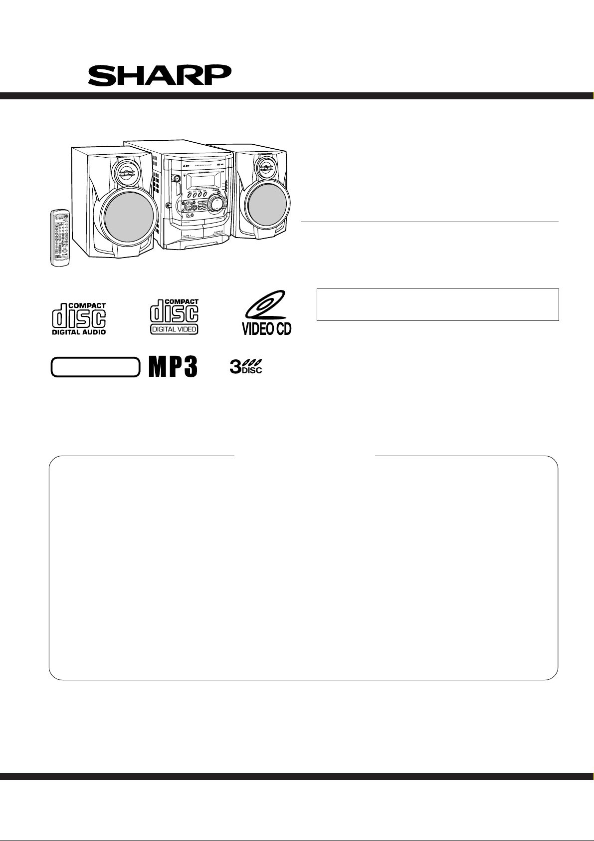
CD-XP205V
SERVICE MANUAL
No. S7256CDXP205V
VIDEO CD MINI SYSTEM
MODEL CD-XP205V
CD-XP205V Video CD Mini System consisting of CD-XP205V
(main unit) and CP-XP205 (speaker system).
• In the interests of user-safety the set should be restored to its
original condition and only parts identical to those specified be
used.
NTSC/PAL
CONTENTS
Page
SAFETY PRECAUTION FOR SERVICE MANUAL ........................................................................................................... 2
VOLTAGE SELECTION..................................................................................................................................................... 2
AC POWER SUPPLY CORD AND AC PLUG ADAPTOR ................................................................................................. 2
SPECIFICATIONS ............................................................................................................................................................. 3
NAMES OF PARTS ........................................................................................................................................................... 4
DISASSEMBLY.................................................................................................................................................................. 6
REMOVING AND REINSTALLING THE MAIN PARTS..................................................................................................... 9
ADJUSTMENT ................................................................................................................................................................. 10
BLOCK DIAGRAM ........................................................................................................................................................... 15
SCHEMATIC DIAGRAM / WIRING SIDE OF P.W.BOARD............................................................................................. 18
NOTES ON SCHEMATIC DIAGRAM .............................................................................................................................. 39
TYPES OF TRANSISTOR AND LED............................................................................................................................... 39
VOLTAGE ........................................................................................................................................................................ 40
WAVEFORMS OF CD CIRCUIT...................................................................................................................................... 41
TROUBLESHOOTING ..................................................................................................................................................... 42
FUNCTION TABLE OF IC................................................................................................................................................ 46
FL DISPLAY..................................................................................................................................................................... 56
REPLACEMENT PARTS LIST/EXPLODED VIEW
SHARP CORPORATION
This document has been published to be used
for after sales service only.
The contents are subject to change without notice.
Page 2
CD-XP205V
SAFETY PRECAUTION FOR SERVICE MANUAL
WARNINGS
THE AEL (ACCESSIBLE EMISSION LEVEL) OF THE LASER POWER OUTPUT IS LESS THAN CLASS 1 BUT THE LASER
COMPONENT IS CAPABLE OF EMITTING RADIATION EXCEEDING THE LIMIT FOR CLASS 1. THEREFORE IT IS
IMPORTANT THAT THE FOLLOWING PRECAUTIONS ARE OBSERVED DURING SERVICING TO PROTECT YOUR EYES
AGAINST EXPOSURE TO THE LASER BEAM.
1-WHEN THE CABINET IS REMOVED, THE POWER IS TURNED ON WITHOUT A COMPACT DISC IN POSITION AND THE
PICKUP IS ON THE OUTER EDGE THE LASER WILL LIGHT FOR SEVERAL SECONDS TO DETECT A DISC. DO NOT
LOOK INTO THE PICKUP LENS.
2-THE LASER POWER OUTPUT OF THE PICKUP UNIT AND REPLACEMENT SERVICE PARTS ARE ALL FACTORY
PRESET BEFORE SHIPMENT.
DO NOT ATTEMPT TO READJUST THE LASER PICKUP UNIT DURING REPLACEMENT OR SERVICING.
3-UNDER NO CIRCUMSTANCES STARE INTO THE PICKUP LENS AT ANY TIME.
4-CAUTION-USE OF CONTROLS OR ADJUSTMENTS, OR PERFORMANCE OF PROCEDURES OTHER THAN THOSE
SPECIFIED HEREIN MAY RESULT IN HAZARDOUS RADIATION EXPOSURE.
Laser Diode Properties
Material: GaAIAs
Wavelength: 780 nm
Emission Duration: continuous
Laser Output: max. 0.6 mW
VOLTAGE SELECTION
Before operating the unit on mains, check the preset voltage. If the voltage is different from your local voltage, adjust the voltage
as follows.
Turn the selector with a screwdriver until the appropriate voltage number appears in the window (110 V, 127 V, 220 V or 230 V - 240 V AC).
AC POWER SUPPLY CORD AND AC PLUG ADAPTOR
QACCE0012AW00
QACCA0003AW00
QPLGA0003AWZZ
QPLGA0004AWZZ
– 2 –
Page 3
CD-XP205V
CD-XP205V
FOR A COMPLETE DESCRIPTION OF THE OPERATION OF THIS UNIT, PLEASE REFER
TO THE OPERATION MANUAL.
SPECIFICATIONS
General
Power source AC 110/127/220/230 - 240 V, 50/60 Hz
Power consumption 133 W
Dimensions Width: 270 mm (10-5/8")
Weight 7.5 kg (16.5 lbs.)
Height: 330 mm (13")
Depth: 355 mm (13-15/16")
Amplifier
Output power MPO: 240 W (120 W + 120 W) (10 % T.H.D.)
Output terminals Speakers: 6 ohms
Input terminals Video/Auxiliary (audio signal): 500 mV/47 k ohms
RMS: 150 W (75 W + 75 W) (10 % T.H.D.)
RMS: 104 W (52 W + 52 W) (0.9 % T.H.D.)
Headphones: 16 - 50 ohms (recommended: 32 ohms)
Video out: 1 Vp-p (75 ohms)
Microphone: 1 mV/600 ohms
Video CD
Video output format PAL/NTSC
CD player
Type 3-disc multi-play compact disc player
Signal readout Non-contact, 3-beam semiconductor laser pickup
D/A converter 1-bit D/A converter
Frequency response 20 - 20,000 Hz
Dynamic range 90 dB (1 kHz)
Tuner
Frequency range FM: 88 - 108 MHz
AM: 531 - 1,602 kHz
Cassette deck
Frequency response 50 - 14,000 Hz (Normal tape)
Signal/noise ratio 55 dB (TAPE 1, playback)
Wow and flutter 0.3 % (WRMS)
CP-XP205
Type 2-way type speaker system
Maximum input power 150 W
Rated input power 75 W
Impedance 6 ohms
Dimensions Width: 220 mm (8-11/16")
Weight 3.0 kg (6.6 lbs.)/each
Specifications for this model are subject to change without
prior notice.
50 dB (TAPE 2, recording/playback)
5 cm (2") Tweeter
13 cm (5-1/8") Woofer
Height: 330 mm (13")
Depth: 222 mm (8-6/8")
– 3 –
Page 4
CD-XP205V
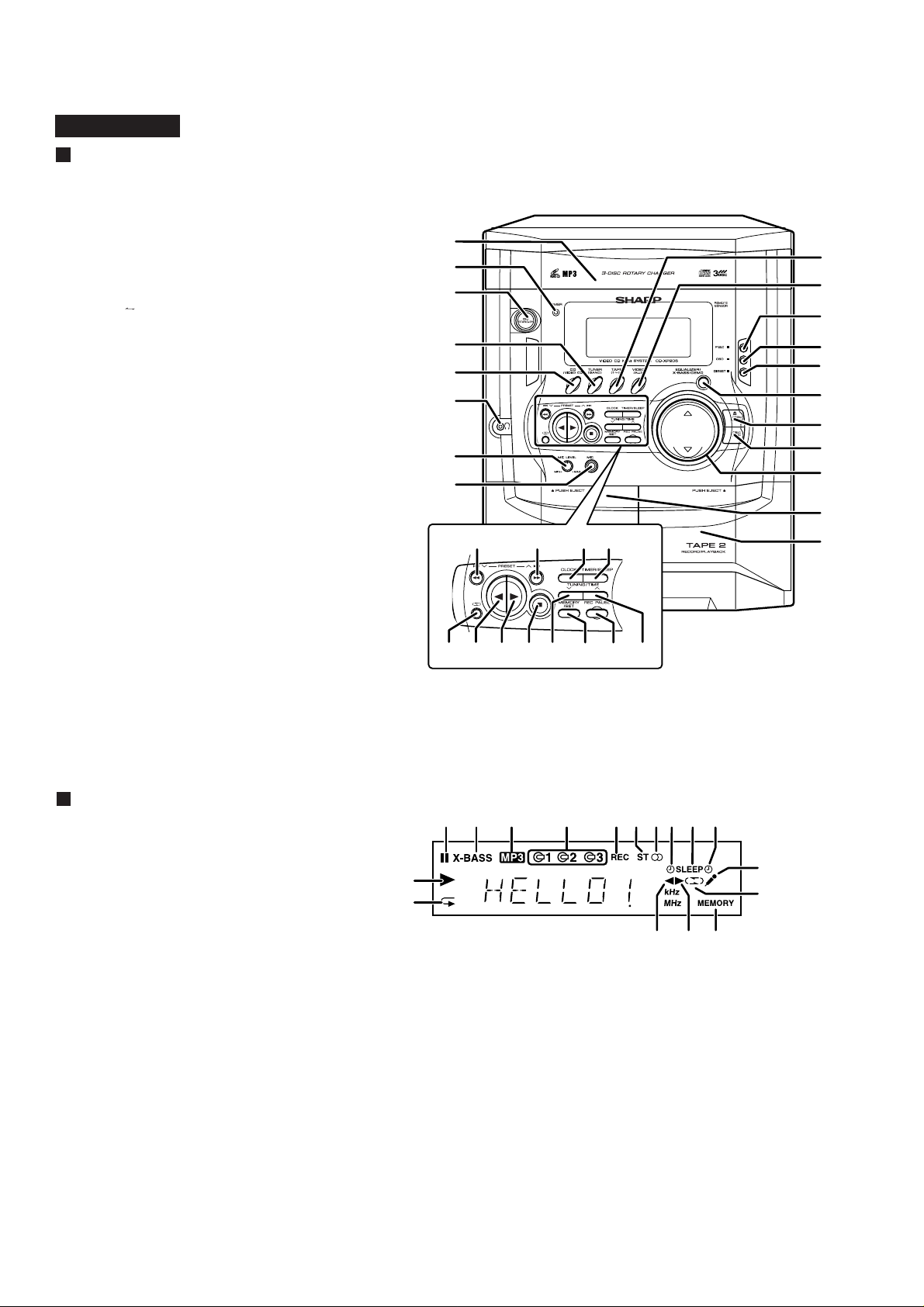
y
NAMES OF P ARTS
CD-XP205V
Front panel
1. Disc Tray
2. Timer Set Indicator
3. On/Stand-by Button
4. Tuner (Band) Button
5. Video CD/CD/MP3 Disc Button
6. Headphone Socket
7. Microphone Level Control
8. Microphone Socket
9. Tape (1 2) Button
10. Video/Auxiliary Button
11. Video CD Playback Control Button
12. Video CD On Screen Display On/Off Button
13. Video CD Digest/Time Search Button
14. Equaliser Mode Select/Extra Bass/Demo Mode Button
15. Disc Tray Open/Close Button
16. Disc Skip Button
17. Volume Up and Down Buttons
18. Tape 1 Cassette Compartment
19. Tape 2 Cassette Compartment
20. Video CD Skip or Previous,
CD/MP3 Disc Track Down or Fast Reverse,
Tape 2 Fast Wind, Tuner Preset Down Button
21. Video CD Skip or Next,
CD/MP3 Disc Track Up or Fast Forward,
Tape 2 Fast Wind, Tuner Preset Up Button
22. Clock Button
23. Timer/Sleep Button
24. Tape 2 Reverse Mode Select Button
25. Tape 2 Reverse Play Button
26. Video CD Play or Repeat or Select or Resume,
CD/MP3 Disc Play or Repeat, Tape 1 Play,
Tape 2 Forward Play Button
27. Video CD Stop or Return,
CD/MP3 Disc/Tape Stop Button
28. Tuning and Time Down Button
29. Memory/Set Button
30. Tape 2 Record Pause Button
31. Tuning and Time Up Button
1
2
3
9
10
11
4
5
6
12
13
14
15
7
16
17
8
18
20
26 2728 313029
2524
2221 23
19
Display
1. Disc Pause Indicator
2. Extra Bass Indicator
3. MP3 Disc Indicator
4. Disc Number Indicators
5. Tape 2 Record Indicator
6. FM Stereo Mode Indicator
7. FM Stereo Receiving Indicator
8. Timer Play Indicator
9. Sleep Indicator
10. Timer Recording Indicator
11. Disc Play Indicator
12. Disc Repeat Play Indicator
13. Karaoke Mode Indicator
14. Tape Reverse Mode Indicator
15. Tape 2 Reverse Play Indicator
16. Tape 1 Play or Tape 2 Forward Play Indicator
17. Memor
Indicator
11
12
2678103 451 9
13
14
15 16 17
– 4 –
Page 5
CD-XP205V
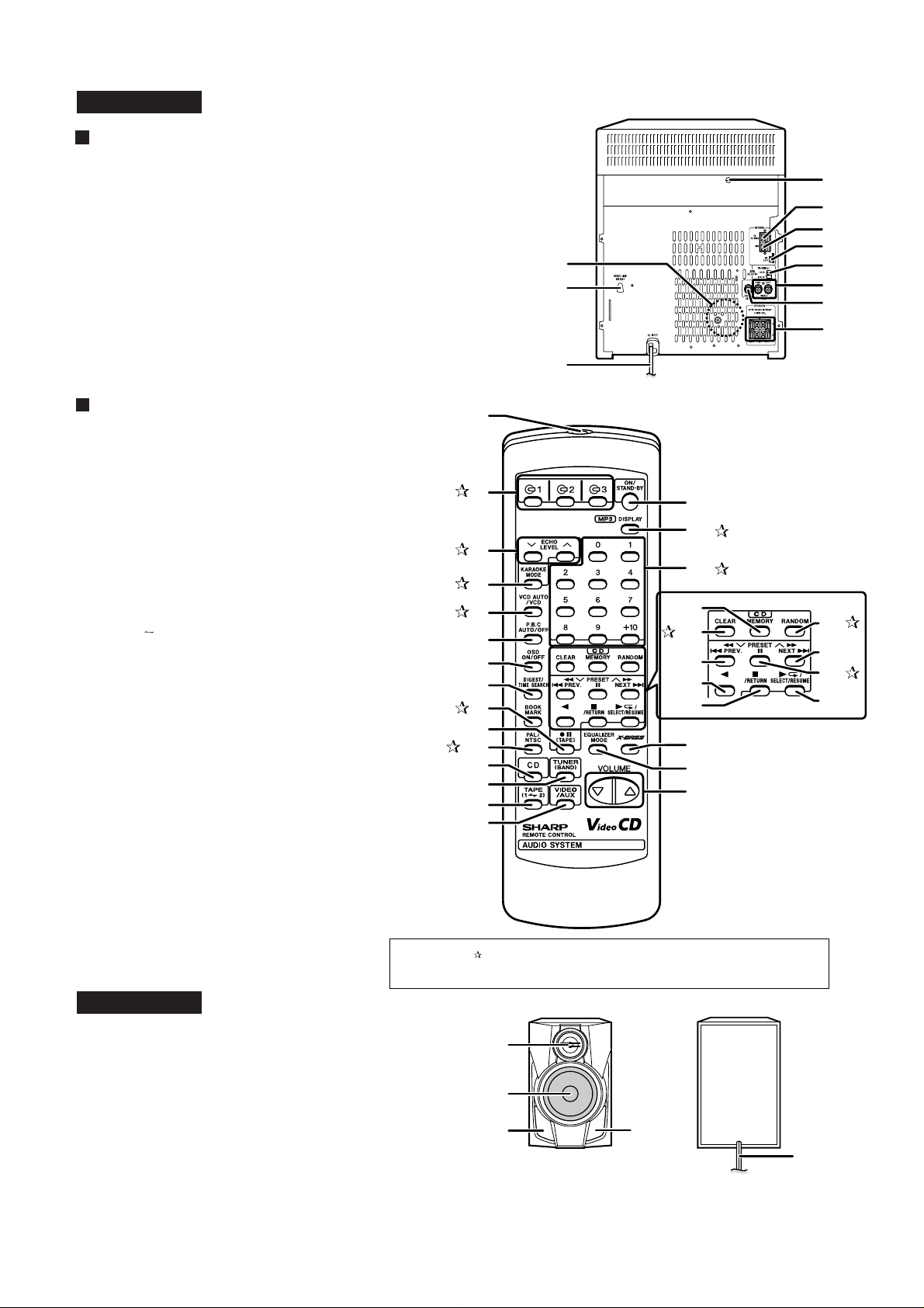
Rear panel
CD-XP205V
1. Cooling Fan
2. AC Voltage Selector
3. AC Power Lead
4. Transport Screw
5. FM 75 Ohms Aerial Terminal
6. FM Aerial Earth Terminal
7. AM Loop Aerial Socket
8. Span Selector Switch
9. Video/Auxiliary (Audio Signal) Input Sockets
10. Video Output Socket
11. Speaker Terminals
Note:
This product is equipped with a cooling fan inside, which begins to run at a specified
volume level for better heat radiation.
Remote control
1. Remote Control Transmitter
2. Disc Number Select Buttons
3. Echo Level Up and Down Buttons
4. Karaoke Mode Button
5. Video CD Auto/On Button
6. Video CD Playback Control Auto/Off Button
7. Video CD On Screen Display On/Off Button
8. Video CD Digest/Time Search Button
9. Video CD Bookmark Button
10. Tape 2 Record Pause Button
11. PAL/NTSC Select Button
12. Video CD/CD/MP3 Disc Button
13. Tuner (Band) Button
14. Tape (1 2) Button
15. Video/Auxiliary Button
16. On/Stand-by Button
17. MP3 Disc Display Button
18. Disc Direct Search Buttons
19. Extra Bass Button
20. Equaliser Mode Select Button
21. Volume Up and Down Buttons
22. Disc Memory Button
23. Disc Clear Button
24. Video CD Skip or Previous,
CD/MP3 Disc Track Down or Fast Reverse,
Tape 2 Fast Wind, Tuner Preset Down Button
25. Tape 2 Reverse Play Button
26. Video CD Stop or Return,
CD/MP3 Disc/Tape Stop Button
27. Disc Random Button
28. Video CD Skip or Next,
CD/MP3 Disc Track Up or Fast Forward,
Tape 2 Fast Wind, Tuner Preset Up Button
29. Disc Pause Button
30. Video CD Play or Repeat or Select or Resume,
CD/MP3 Disc Play or Repeat, Tape 1 Play,
Tape 2 Forward Play Button
CP-XP205
1. Tweeter
2. Woofer
3. Bass Reflex Duct
4. Speaker Wire
Buttons with " " mark in the illustration can be operated on the remote control
only.
1
2
3
4
5
6
7
8
9
10
11
12
13
14
15
1
2
4
5
6
7
1
2
8
9
10
11
3
16
17
18
22
23
24
25
26
27
28
29
30
19
20
21
– 5 –
3
3
4
Page 6
CD-XP205V
DISASSEMBLY
Caution on Disassembly
Follow the below-mentioned notes when disassembling
the unit and reassembling it, to keep it safe and ensure
excellent performance:
1. Take cassette tape and compact disc out of the unit.
2. Be sure to remove the power supply plug from the wall
outlet before starting to disassemble the unit.
3. Take off nylon bands or wire holders where they need to
be removed when disassembling the unit. After servicing
the unit, be sure to rearrange the leads where they were
before disassembling.
4. Take sufficient care on static electricity of integrated
circuits and other circuits when servicing.
CD-XP205V
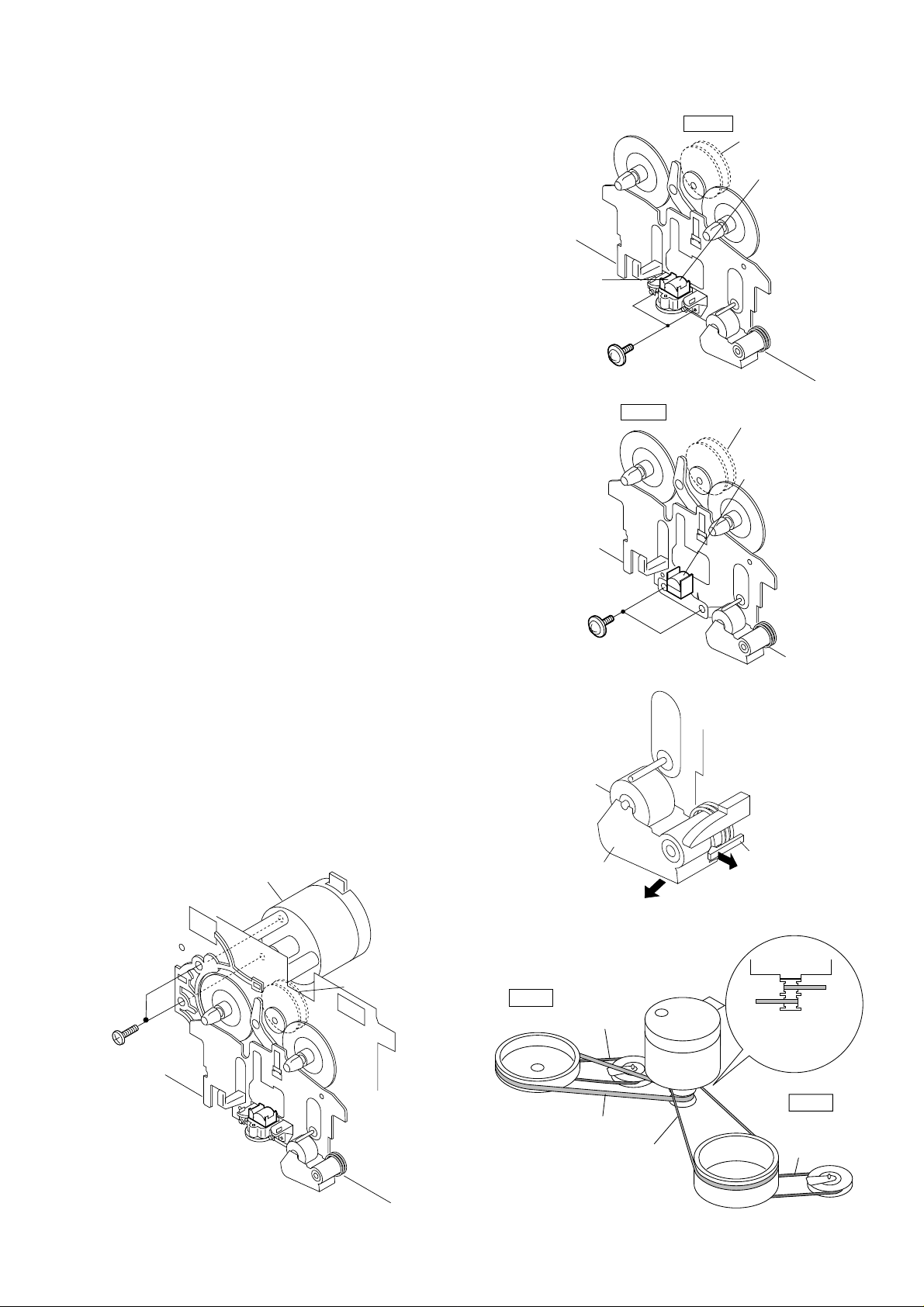
STEP
10
11 Turntable 1. Hook.........................(L1) x2 7-3
12 Loading Tray 1.
13 Video CD PWB 1. Screw ...................... (N1) x2 7-5
14 CD Mechanism 1. Hook ........................ (P1) x2 7-6
Note 1: How to open the changer manually. (Fig. 6-3)
1. In this state, turn fully the lock lever in the arrow direction through
2. After that, push forward the loading tray.
REMOVAL PROCEDURE FIGURE
1 Top Cabinet 1. Screw ...................... (A1) x4 6-1
2 Side Panel 1. Screw ...................... (B1) x8 6-1
(Left/Right)
3 CD Tray Cover/ 1. Turn on the power supply, .. 6-2
CD Player Unit open the disc tray, take out
4 Rear Panel with 1. Screw .................... (D1) x12 6-2
Fan Motor 2. Socket ..................... (D2) x1
5 Main PWB 1. Screw ...................... (E1) x4
6 Front Panel 1. Screw .......................(F1) x2 7-1
7 Mic PWB 1. Screw ...................... (G1) x2 7-1
8 Display PWB 1. Screw .................... (H1) x12 7-2
9 Tape Mechanism 1. Open the cassette holder. 7-2
Headphones PWB
(Note 2) 2. Hook........................ (N2) x1
the hole on the loading tray bottom.
the CD tray cover, and close.
(Note 1)
2. Screw ...................... (C1) x1
3. Hook........................ (C2) x3
4. Hook........................ (C3) x2
5. Socket ..................... (C4) x4
2. Socket ..................... (E2) x4 7-1
3. Flat Cable ............... (E3) x1
4. Flat Wire.................. (E4) x1
2. Hook.........................(F2) x2
3. Socket ......................(F3) x1
2. Tip Wire................... (G2) x1
2. Flat Cable ............... (H2) x1
2. Screw...................... (J1) x5
1. Screw ...................... (K1) x1 7-2
2. Cover .......................(L2) x1
Turn fully the lock lever in the
arrow direction
2.
Push the loading tray backward
to engage the claw with the
groove and remove it in the
direction of the arrow..(M1) x6
3. Socket ..................... (N3) x4
2. Hook........................ (P2) x2
.
6-2, 7-1
6-3
7-4
CD-XP205V
Side Panel
(Right)
(B1)x2
ø3x10mm
(B1)x4
ø3x10mm
VIDEO
CD PWB
(C3)x1
Pull
Rear
Panel
(C1)x1
ø3x10mm
Lock Lever
CD Player Unit
(Bottom View)
(A1)x2
ø3x12mm
(C4)x4
(D1)x11
ø3x10mm
Top Cabinet
Rear
Panel
Figure 6-1
Main
PWB
Figure 6-2
CD Tray Cover
2
1
(D2)x1
(E1)x1
ø3x10mm
Front
Panel
(B1)x2
ø3x10mm
(D1)x1
ø3x10mm
(A1)x2
ø3x12mm
Side Panel
(Left)
(C2)x3
1
2
CD Player
Unit
(C3)x1
Main PWB
Lug Wire
(E1)x1
ø3x10mm
Note 2:
1. After removing the connector for the optical pickup from the
connector, wrap the conductive aluminium foil around the front end
of the connector so as to protect the optical pickup from electrostatic damage.
Figure 6-3
Note 3:
1. Be careful not to break the claw of the CD mechanism.
2. When fining back the cam gear assembly, let it lock by front
movement.
– 6 –
Page 7
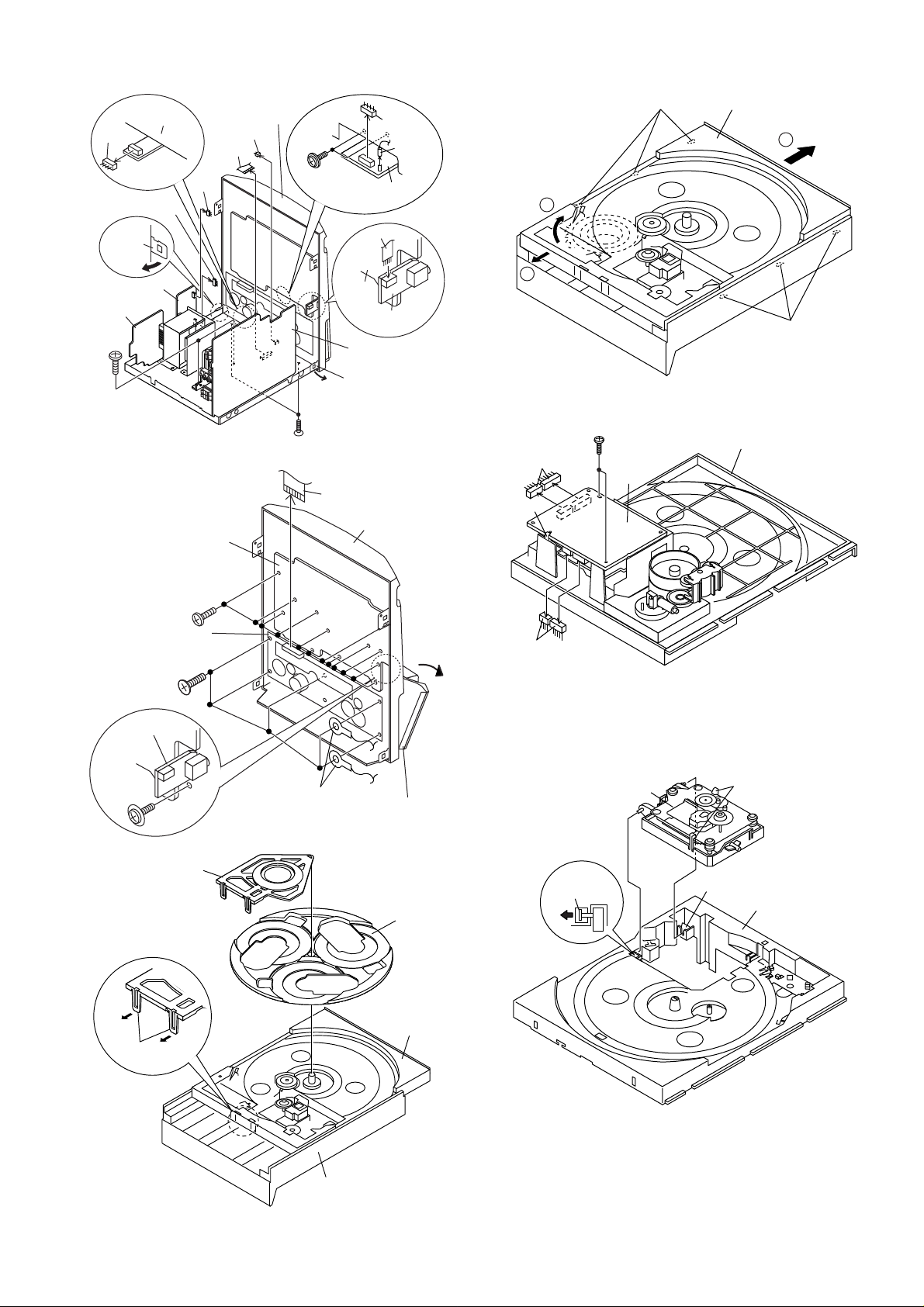
CD-XP205V
Tape
Mechanism
(E2)x1
(F2)x1
Power PWB
Transformer
PWB
(E1)x2
ø3x10mm
(E2)x1
(E2)x1
(E3)x1
(F3)x1
Figure 7-1
Display PWB
Front
Panel
(G1)x2
ø3x10mm
Display
PWB
(F2)x1
(F1)x2
ø3x10mm
(H2)x1
(E2)x1
(G2)x1
Mic
PWB
(E4)x1
Headphones
PWB
Main PWB
Front Panel
1
(N3)x2
(N2)x1
(M1)x3
Loading Tray
3
2
(M1)x3
Figure 7-4
(N1)x2
ø3x10mm
Video CD
PWB
Loading
Tray
(J1)x5
ø3x10mm
Headphones
PWB
(K1)x1
ø3x10mm
(L1)x2
(H1)x12
ø3x10mm
Tape
Mechanism
(L2)x1
Figure 7-2
Lug Wire
Cassette
Holder
Turntable
Loading
Tray
Open
(N3)x2
(P1)x1
CD
Mechanism
Figure 7-5
(P2)x2
(P1)x1
Loading Tray
Figure 7-3
Figure 7-6
CD Player Unit
– 7 –
Page 8
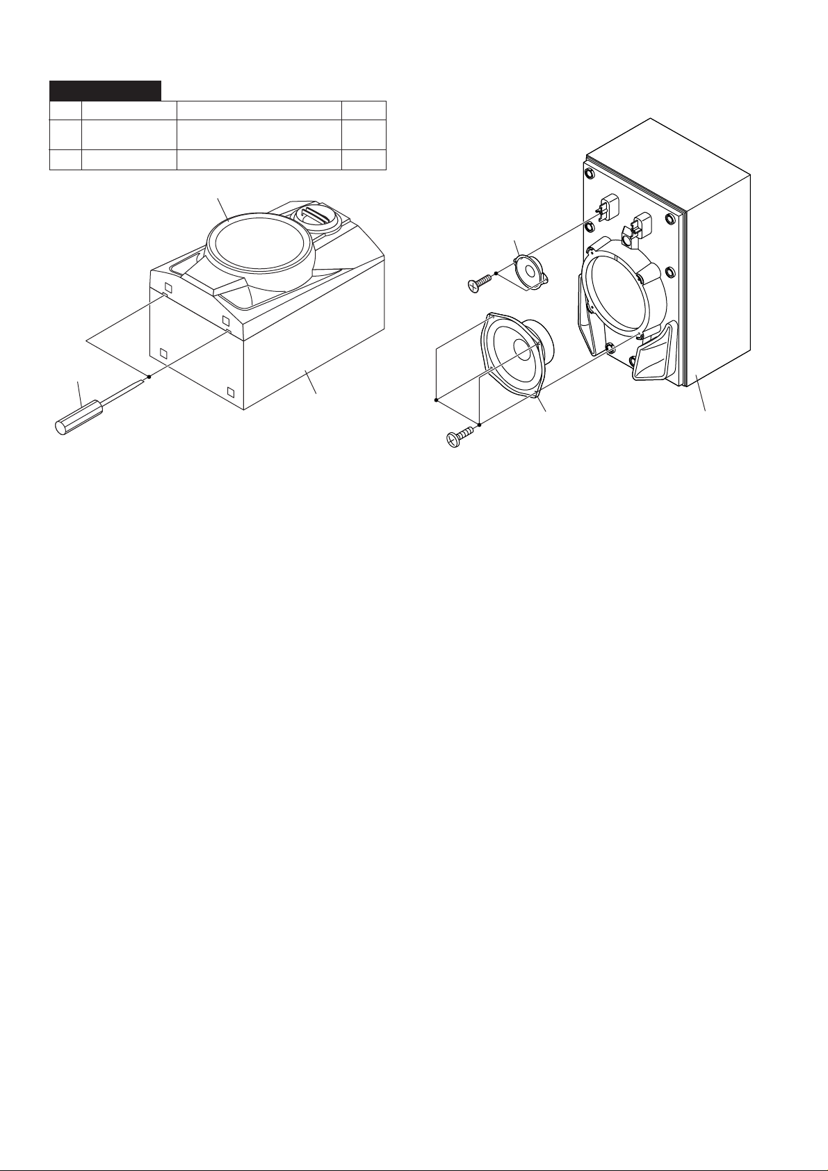
CD-XP205V
CP-XP205
STEP
Screwdriver
REMOVAL PROCEDURE FIGURE
1 Woofer 1. Front Panel ............. (A1) x1 8-1
2 Tweeter 1. Screw ...................... (B1) x2 8-2
Driver should
be pried away
from Speaker Box.
2. Screw ...................... (A2) x4 8-2
(A1)x1
Speaker Box
Ass'y
(B1)x2
ø3x10mm
Tweeter
(A2)x4
ø4x12mm
Woofer
Speaker Box
Ass'y
Figure 8-1 Figure 8-2
– 8 –
Page 9
REMOVING AND REINSTALLING THE MAIN PARTS
TAPE 2
TAPE 1
Main Belt
(E1)x1
TAPE 2
Main Belt
(D1)x1
TAPE 1
Main Belt
(D1)x1
Main Belt
(E1)x1
FF/REW
Belt
(D2)x1
FF/REW
Belt
(E2)x1
Tape
Motor
Tape
Motor
TAPE MECHANISM SECTION
Perform steps 1 to 6 and 9 of the disassembly method to
remove the tape mechanism.
How to remove the record/playback and erase
heads (TAPE 2) (See Fig. 9-1)
1. When you remove the screws (A1) x 2 pcs., the record/
playback head and three-dimensional head of the erasing
head can be removed.
How to remove the playback head (TAPE 1)
(See Fig. 9-2)
1. When you remove the screws (B1) x 2 pcs., the playback
head can be removed.
How to remove the pinch roller (TAPE 1/2)
(See Fig. 9-3)
1. Carefully bend the pinch roller pawl in the direction of the
arrow <A>, and remove the pinch roller (C1) x 1 pc., in the
direction of the arrow <B>.
Note:
When installing the pinch roller, pay attention to the spring
mounting position.
Erase Head
(A1)x2
Ø2x9mm
Figure 9-1
TAPE 1
TAPE 2
CD-XP205V
Clutch Ass'y
Record/Playback
Head
Clutch Ass'y
Playback
Head
How to remove the belt (TAPE 2)
(See Fig. 9-4)
1. Remove the main belt (D1) x 1 pc., from the tape motor side.
2. Remove the FF/REW belt (D2) x 1 pc.
How to remove the belt (TAPE 1)
(See Fig. 9-4)
1. Remove the main belt (E1) x 1 pc., from the tape motor side.
2. Remove the FF/REW belt (E2) x 1 pc.
How to remove the tape motor (See Fig. 9-5)
1. Remove the screws (F1) x 2 pcs., to remove the tape motor.
Tape Motor
Clutch Ass'y
(F1)x2
Ø2.6x5mm
(B1)x2
Ø2x9mm
Pinch Roller
(C1)x1
Figure 9-2
Pull
Figure 9-3
<B>
<A>
Pinch
Roller
Pawl
Figure 9-4Figure 9-5
– 9 –
Page 10
CD-XP205V
(B3)x2
ø2.6x6mm
Shaft
(B4)x1
Stop Washer
(B1)x1
Gear
(B2)x1
CD Mechanism
Pickup
CD MECHANISM SECTION
Perform steps 1, 2, 3, 11, 12, 13 and 14 of the disassembly
method to remove the CD mechanism.
How to remove the loading motor
(See Fig. 10-1)
1. Remove the screw (A1) x 1 pc., to bend the hooks (A2) x 5
pcs., to remove the loading motor.
How to remove the pickup (See Fig. 10-2)
1. Remove the stop washer (B1) x 1 pc., to remove the gear
(B2) x 1 pc.
2. Remove the screws (B3) x 2 pcs., to remove the shaft
(B4) x 1 pc.
3. Remove the pickup.
Note
After removing the connector for the optical pickup from the
connector wrap the conductive aluminium foil around the front
end of connector so as to protect the optical pickup from
electrostatic damage.
Loading
Tray
Loading
Motor PWB
Loading
Motor
Figure 10-1
(A1)x1
ø3x10mm
(A2)x5
MECHANISM SECTION
••
• Driving Force Check
••
Play: TW-2111 Tape 1: Over 80 g
••
• Torque Check
••
Play: TW-2111 30 to 80 g.cm 30 to 80 g.cm
Fast forward: TW-2231 — 70 to 180 g.cm
Rewind: TW-2231 — 70 to 180 g.cm
Torque Meter Specified Value
Tape 2: Over 80 g
Torque Meter
Specified Value
Tape 1
ADJUSTMENT
Tape 2
Figure 10-2
••
• Tape Speed
••
Test Tape
Normal MTT-111 Variable 3,000 ± 30 Hz Speaker
speed Resistor in Terminal
Adjusting
Point
motor. (Load
Specified
Value
Instrument
Connection
resistance:
6 ohms)
TAPE MECHANISM
Tape
Motor
Variable Resistor in motor
Figure 10-3
– 10 –
Page 11
CD-XP205V
T
T
EFBL
FDO
TE
Stopped
CH1=500 mV
DC 10:1
CH2=200 mV
DC 10:1
CH3=1 V
DC 10:1
500 ms/div
(500 ms/div)
NORM:20 kS/s
1
2
3
=Record Length=
Smoothing : ON CH1 : 0.000 V
CH2 : 0.000 V
Main : 100K
Zoom : 2k
Mode : SINGLE
Type : EDGE CH1
Delay : 0.0 ns
Hold off : 0.2 µs
CH3 : 0.00 V
CH4 : 0.00 V
BW : FULL
=Trigger==Filter= =Offset=
CH2
v/DIV
200 mV
1999/04/05 20:26:47
TUNER SECTION
fL: Low-range frequency
fH: High-range frequency
••
•
AM IF/RF
••
Signal generator: 400 Hz, 30%, AM modulated
Test Stage Frequency Frequency
Display
AM IF 450 kHz 1,602 kHz T351 *1
AM Band — 531 kHz (fL): T306 *2
Coverage 1.1 ± 0.1 V
AM Tracking 990 kHz 990 kHz (fL): T303 *1
*1. Input: Antenna Output: TP302
*2. Input: Antenna Output: TP301
••
• FM RF
••
Signal generator: 1 kHz, 40 kHz dev., FM modulated
Test Stage
FM Band — 87.50 MHz T301 (fL): *1
Coverage 1.3 V ± 0.1 V
FM RF 98.00 MHz 98.00 MHz L312 *2
Frequency Frequency
Display
(10-30 dB)
*1. Input: Antenna Output: TP301
*2. Input: Antenna Output: Speaker terminal
••
• FM IF
••
Signal generator: 10.7 MHz, FM modulated
Test Stage Instrument
IF 10.7 MHz 98.00 MHz T302 *1
Frequency Frequency
Display
*1. Input: Antenna Output: TP301
Setting/
Adjusting
Parts
Setting/
Adjusting
Point
Setting/
Adjusting
Point
(Turn the
core of transformer T302
fully counterclock wise)
Instrument
Connection
Instrument
Connection
Connection
CD SECTION
• Adjustment
Since this CD system incorporates the following automatic
adjustment functions, readjustment is not needed when
replacing the pickup. Therefore, different PWBs and pickups
can be combined freely.
Each time a disc is changed, these adjustments are
performed automatically. Therefore, playback of each disc
can be performed under optimum conditions.
Items adjusted automatically
(1) Offset adjustment (The offset voltage between the head
amplifier output and the VREF reference voltage is
compensated inside the IC.)
* Focus offset adjustment
* Tracking offset adjustment
(2) Tracking balance adjustment (waveform drawing
Fig. 11-2 EFBL)
(3) Gain adjustment (The gain is compensated inside the IC
so that the loop gain at the gain crossover frequency will
be 0 dB.)
* Focus gain adjustment
* Tracking gain adjustment
CD ERROR CODE DESCRIPTION
Error Explanation
01
10*
11* "CLAMP SW", "DISC NO SW" and "OPEN/CLOSE"
31
* 'CHECKING'
If Error is detected, 'CHECKING' will be display instead of 'ERCD**' display. 'ER-CD**' display will only be display when
error had been detected for the 5 th times.
When Pickup set inner position, inner switch
cannot detect 'ON' level for 10 secs.
When tray moves to Open/Close, Open/Close switch
cannot detect 'ON' level for 7 secs.
When disc table rotate to target position.
Clamp switch cannot detect 'ON' level for 7 secs.
When disc table set to Disc1 position for 1 st time,
cannot detect 'ON' level for 14 secs.
When it changes to CD function, DSP cannot read
initial data.
MAIN PWB
SO302
TERMINAL
FM ANTENNA
CNP302
ANTENNA
AM/FM LOOP
FM BAND
COVERAGE fL
T302
IC301
1
L312
R316
T303
AM TRACKING
fL
Figure 11-1 ADJUSTMENT POINTS
T301
FM IF
FM RF
TP301
T306
AM BAND
COVERAGE fL
T351
AM IF
TP302
R356
Figure 11-2
– 11 –
Page 12
CD-XP205V
TEST MODE
• Setting the test mode
Any one of test mode can be set by pressing several keys as follows.
<X-BASS> + <CD> + <POWER> TEST: CD operation test.
Function: -CD test mode.
-Enter test mode.
C D T E S T
OPEN/CLOSE operation is using manual.
<< >>, << >> buttons make pick's slide possible.
IL isn't done
<<MEMORY>>
key input.
Adjustment result
automatically will
display as below.
for each 2 sec :
a) "FOFF_XX"
b) "TOFF_XX"
c) "TBAL_XX"
d) "TGAN_XX"
f) "FGAN_XX"
g) "RFLS_XX"
explanation:
a) Focus off set = "FOFF_XX"
b) Tracking off set = "TOFF_XX"
c) Tracking balance = "TBAL_XX"
d) Tracking Gain = "TGAN_XX"
f) Focus Gain = "FGAN_XX"
g) RF level shift = "RFLS_XX"
<<PLAY>> key input.
Do TOC IL. Do normal play.
When these following key is input
into PLAY key, track number can
be appoint directly.
<< 1>> key: Track 4
<<
2>> key: Track 9
<<
3>> key: Track 15
<<STOP>> key input.
STOP
<<MEMORY>> key input.
Laser ON.
<<MEMORY>> key input.
Tracking OFF play at that
specific point.
<<MEMORY>> key input.
Tracking ON play from
that specific point.
<<MEMORY>> key input.
Adjustment result automatically will
display as below for each 2 sec :
a) "FOFF_XX"
b) "TOFF_XX"
c) "TBAL_XX"
d) "TGAN_XX"
f) "FGAN_XX"
g) "RFLS_XX"
<<STOP>> key input.
VOL — Last memory
BAL — CENTER
P.GEQ — FLAT
X-BASS — OFF
To cancel : Power OFF
– 12 –
STOP
Sliding the PICKUP with
<<
>>, << >> button
must only be in STOP mode.
Page 13
CD-XP205V
Standard Specification of Stereo System Error Message Display Contents
Error Contents DISPLAY Notes
TAPE Mechanism Error. 'ER-TA**' 00: Tape Mechanism Error.
01: Initial Error.
CD Pickup Mechanism Error. 'ER-CD**' 01: PU-IN SW Detection NG.
CD Changer Mechanism Error. 'ER-CD**' 10: Changer Error.
(*) 11: Initial Error.
CD DSP Communication Error 'ER-CD**' 31: DSP COMMUNICATION ERROR
Focus Not Match. 'NO DISC'
IL Time Over. 'NOT READ'
TUN PLL Unlock. 'ER-TU**' 00: TUN Error.
01: PLL Unlock.
(*) CHECKING:
If CD changer mechanism error is detected, 'CHECKING' will be display instead of 'ER-CD**' display 'ER-CD**' will only be display
when CD changer mechanism error had been detected for the 5 th times.
Speaker abnormal detection and +B PROTECTION display
In case speaker abnormal detection or +B PROTECTION had occurred, it can be check by pressing 'POWER', 'VIDEO' and 'XBASS' key twice. Display will show "S** B**". S is referring to speaker abnormal detection and B is referring to +B PROTECTION.
** is in hex valve.
+B PROTECTION is condition when irregular process occur on power supply line.
VIDEO CD SECTION
TEST DISC Model No. TVD-581A (NTSC/PAL)
• Checking of video output signal
Checking of color bar
Disc Adjusting Point
Track 2 Video output terminal
Instrument
Connection
Chroma Peak Level
105 ± 15 IRE
UNIT
(0.714 V)
(1 V)
40 IRE
Color Burst
Video Output Terminal
Video Input Terminal
TV
140 IRE
40 IRE
(0.286 V)
100 IRE
20
-20
-40
75
Gray
IH
100 100
33.5
Yellow
(59.94 Hz)
88.5
75
5
0
-13.5
Magenta
Cyan
70
41.5
-25 -25
Red
Green
Color bar signal
waveform
Horizontal
sync signal
Blue
Figure 13-1 CHECKING OF VIDEO OUTPUT SIGNAL Figure 13-2
– 13 –
Page 14
CD-XP205V
Gray
Cyan
Yellow
Magenta
Red
Green
Blue
TV monitor
Figure 14-1
Checking of vector scope waveform
Disc Checking Setting
Set the phase of color
Track 2 VIDEO OUT burst signal (B) to
180° -360° line.
Checking
Item
Phase check
±10°
( Check that the setting is within the illustrated range.)
90
170
180
190
160
200
150
210
140
220
130
230
120
103.4
167.1
YE
240
110
250
100
R
240.8
G
260
270
80
MG
-1
123 +180
CY
280
70
+0
33
283.4
290
60
60.8
BL
300
50
40
30
347.1
330
320
310
Vector scope waveform of color bar signal
Figure 14-2
20
340
10
360
350
Gray
Cyan
Yellow
Magenta
Green
TV monitor
Figure 14-3
Checking the black-and-white level
Disc Checking Setting
Track 3 VIDEO OUT 150 line.
IRE
100
80
60
40
20
-20
-40
NTSC
Waveform on 140 LINE
Figure 14-4
0%
12.5%
100%
Red
Blue
Checking
Item
Output level
±10 IRE
(This burst level
is 40 IRE)
140 IRE
– 14 –
TV monitor
Figure 14-5
Page 15
M3
T/T UP/DOWN
LOADING
MOTOR
SW3
DISC
NUMBER
SW2
CLAMP
SW1
OPEN/
CLOSE
+6.5 V (+B4)
A10 V (+B8)
+5 V (+B7)
TO MAIN
SECTION
DISC NO. SW
CLAMP SW
SECTION
TO DISPLAY
+B12
M
DGND
CD-GND
L-CH
A_GND
R-CH
O/C SW
CD RES
CLK
DO
DRF
WRG
-
+
CNP11
DI
CE
CNP12
CD-XP205V
JK690
84
5
LR
ICM1
35
+
+
-
M
M
VIDEO OUT
+B8
7
L
1
R
22
~
26
31
~
34
36
~
39
20
6
1
40
M1
SPINDLE
MOTOR
M2
SLED
MOTOR
TRACKING COIL
FOCUS COIL
PICKUP UNIT
+B12
94
92
89
96
XL1
27 MHz
98 79 37 33 23 90 78 73 66 60 59
74
XIN
XOUT
71
~
8
81
83
85
93
95
97
99
17
OE_
ICM4
6
5
4
3
2
1
CNP4
24
CE_
22
15
~
13
12
IX0512AW
EPROM IC
~
2
1
6
5
4
3
2
1
+B12
QM6
QM5
~
21
23
25
~
30
32
6
5
4
3
2
1
8
80
86
84
VCD COMPANION
669
DSC_C
+B13
+B12
AJN
ARFS
ARCLK
ICM3
ES3889F
1 25 26 31 41 43 51 56 57 62 45 48
~~
50 30
VIDEO CD DECODER
~
9188
45 44 43 41 3247
ICM2
ES3880F
49 52 54
AJN
55
~
62
64
65
66
68
~
79
80
100
LOE#
LROMCE#
LSC1#
~
8782
TO ICM3
17, 19, 21, 22PIN
4482
LR
ARCLK
959493
CNP1
39
38
42
41
40
25
17
64
53
32
16
5
100
91
77
75
72
63
ARFS
2
1
12
~
4
28
~
13
81
51
31
1
~
OUT6OUT6+
IN6+
IN6-
VCC4
SPDO
SLDO
FDO
TDO
+B12
CNP1
+B12
+B13
2935
IC3
M63001FP
18 24 23 28
QM1
+B8
IC6
TJM4558CD
OPE AMP.
3
19
~
16
10
~
7
1625635T
5
DRAM
~
2
21
~
8142122
SP-
27
SP+
26
SL+
16
SL-
15
TR-
7
TR+
6
FOCUS/TRACKING/
SPIN/SLED DRIVER
FO-
5
FO+
4
7
+B8
6
5
4
3
2
1
10
9
8
7
6
5
4
3
2
1
Q2
Q9
Q10
SW4
PICKUP IN
TEST
40
30
CONT2
CONT3
31
CONT4
32
EMPH
41
CECLDI
SERVO/SIGNAL
DO
RVSS
47
LVSS
46
XVSS
53
CONT6
75
IC2
LC78636E
CONTROL
WRQ
RES
CONT5
DEF
65 66 67 68 70 71 72 52 51
16.9344 MHz
SLDO
XOUT
XL2
FDO
SPDO
XVDD
RVDD
LVDD
ADAVDD
VVDD
XIN
23242526336474
HFL
VDD
VDD
VCC
LASER
DRIVER
IC1
+3.4 V
(+B11)
Q3
LDD
PD
TIN2
LA9235M
TIN1
SERVO AMP.
FIN2
FIN1
8
7
4
3
2
1
+5 V
(+B7)
TDO
19
13
+5 V (+B7)
3
16
TE
15
FE
PH
14
7
50
49
44
36
RFEV
22
FE-
21
20
FE
19
TETE
18
HFL
17
18
5
73
+5 V
(+B7)
VOLTAGE
REGULATOR
+3.4 V (+B11)
Q4
30 23 11 9
+3.4 V
(+B11)
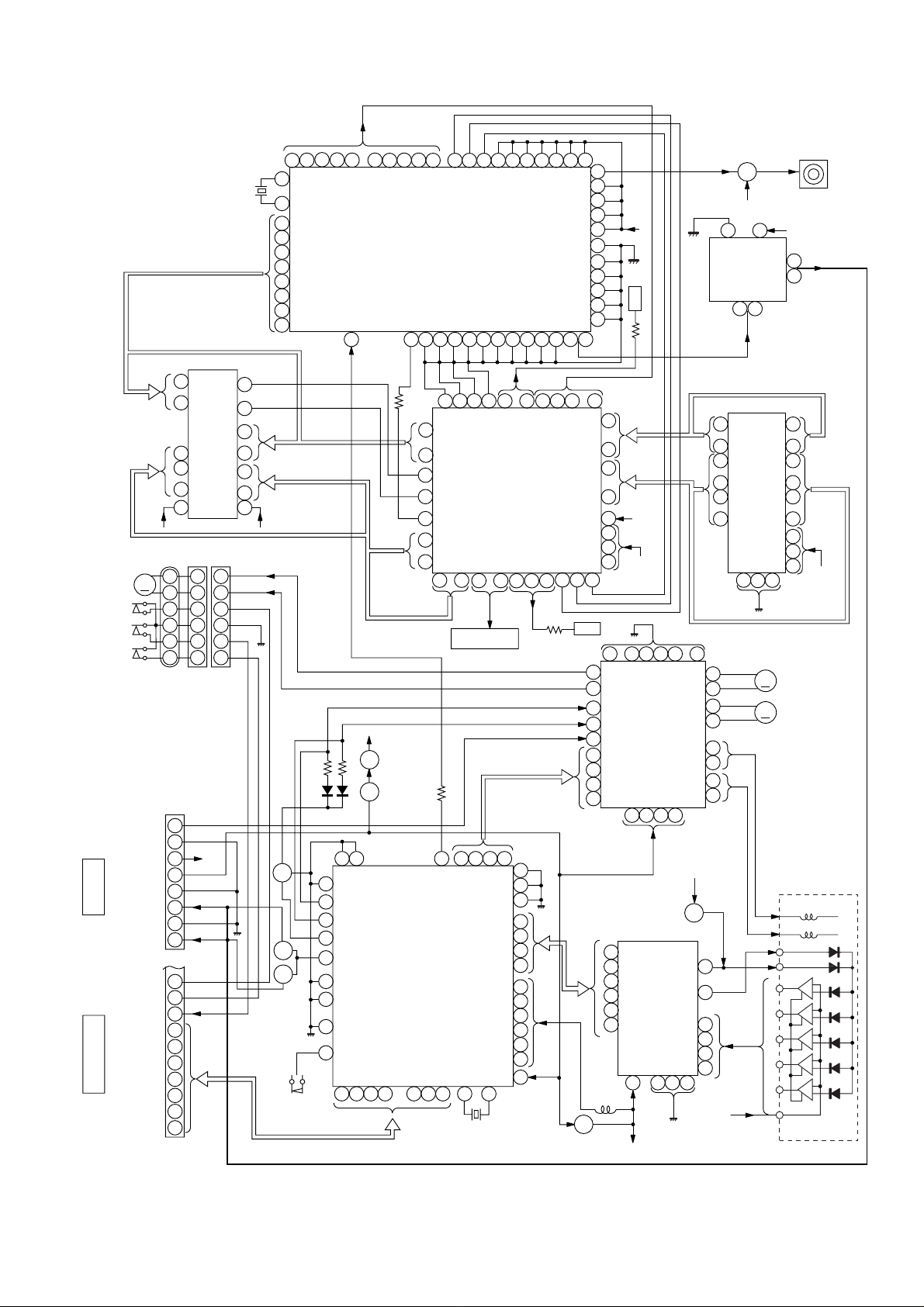
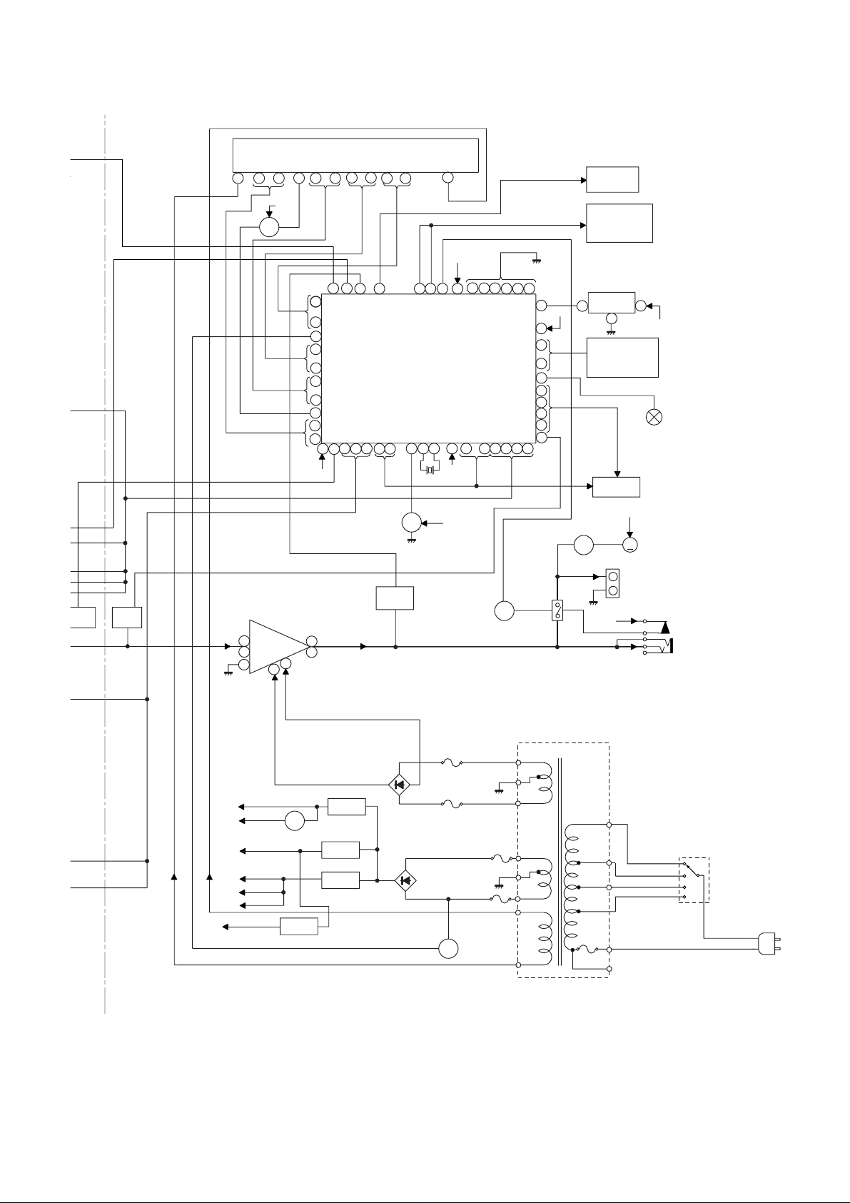
Figure 15 BLOCK DIAGRAM (1/3)
– 15 –
Page 16
CD-XP205V
S
2
JK1
MIC
VRK1
MIC
VOLUME
M65856SP
MIC AMP.
MIC IN
ICK1
ANTENNA
FM ANTENNA
TERMINAL
AM LOOP
ANTENNA
40
LATCH
DATA
CLOCK
9
12
ROUT
13
LOUT
22
TAPE 1
P.B. HEAD
TAPE 2
REC./P.B.
HEAD
FM
SO302
RIN
LIN
VCC
42
41
35
36
32
31
23
L-CH
R-CH
L-CH
R-CH
ERASE
CNP302
HEAD
BF301
B.P.F
KIA4558P
OPE AMP.
6
5
2
3
QK1
CNP11
FROM
CD SECTION
REC.
P.B.
AC BIAS
TA7358AP
FM FRONT END
1
4
3
L312 T301
FM RF
AM TRACKING
T303 T306
ICK2
R
7
1
L
+B5
1
2
3
BI601
L(T1)
R(T1)
L(T2)
R(T2)
SWITCHING
Q101~
Q104
L REC
R REC
SWITCHING
Q105
Q106
+B5
Q111
L103
BIAS/
OSC
IC301
6
8
7
FM
OSC
OSC BUFF
AM BAND
COVERAGE
9
FM
OSC
Q302
5
IC302
LC72131
PLL(TUNER)
FM+B
SWITCHING
1
P.B
24
2
23
H/N
REC
9
16
11
12
NOR/
15
HIGH
T1/T2
19
Q114
SWITCHING
Q112
SWITCHING
Q113
SWITCHING
FM IF
13
4
21
7
18
Q109
+B6
CF303T302
T351
AM IF
21
AM MIX
21
AM OSC IN
AM OSC OUT
AM RF IN
VT
+B5
Q360
+B5
L
PB
R
RECRL
X352
4.5 MHz
20 22 11
OSC
FM
JK690
VIDEO/AUX
L
R
TUNER
7
AUX
TAPE
CD
1615
FM/AM
21
9 10
9
L
16
R
L
10
15
R
L
11
14
R
L
12
13
R
IC101
AN7345K
PLAYBACK AND RECORD
/PLAYBACK AMP.
+B5
Q110
BIAS
+B3
+B3
+B6
ZD351
10.7 MHz
CF351
FM
DET
FM+B
MPXIN
162324
5.1V
X351
456 kHz
13
VCO
L
MO/ST
R
FM/AM
12
14
15
450 kHz
CF352
7
STEREO
LA1832S
+B6
4
98517
GND
AM IF
FM/AM
OUT
18
IC303
FM IF DET./
FM MPX./AM IF
CLK
DO
DI
CE
6
5413
IC601
17
+B5
1
DI
2
CE
24
CLK
MO/ST
LC75341
AUDIO PROCESSOR
8
17
7
18
MOTOR
DRIVER
Q706
Q707
Q708
SOLENOID
DRIVER
3
Q107
Q108
MUTING
R
21
4
L
23
+B5
TAPE
MECHANISM
ASS'Y
–20dB
ATT
+B5
Q601
Q602
REC/PLAY
Q603
Q604
T1/T
BIA
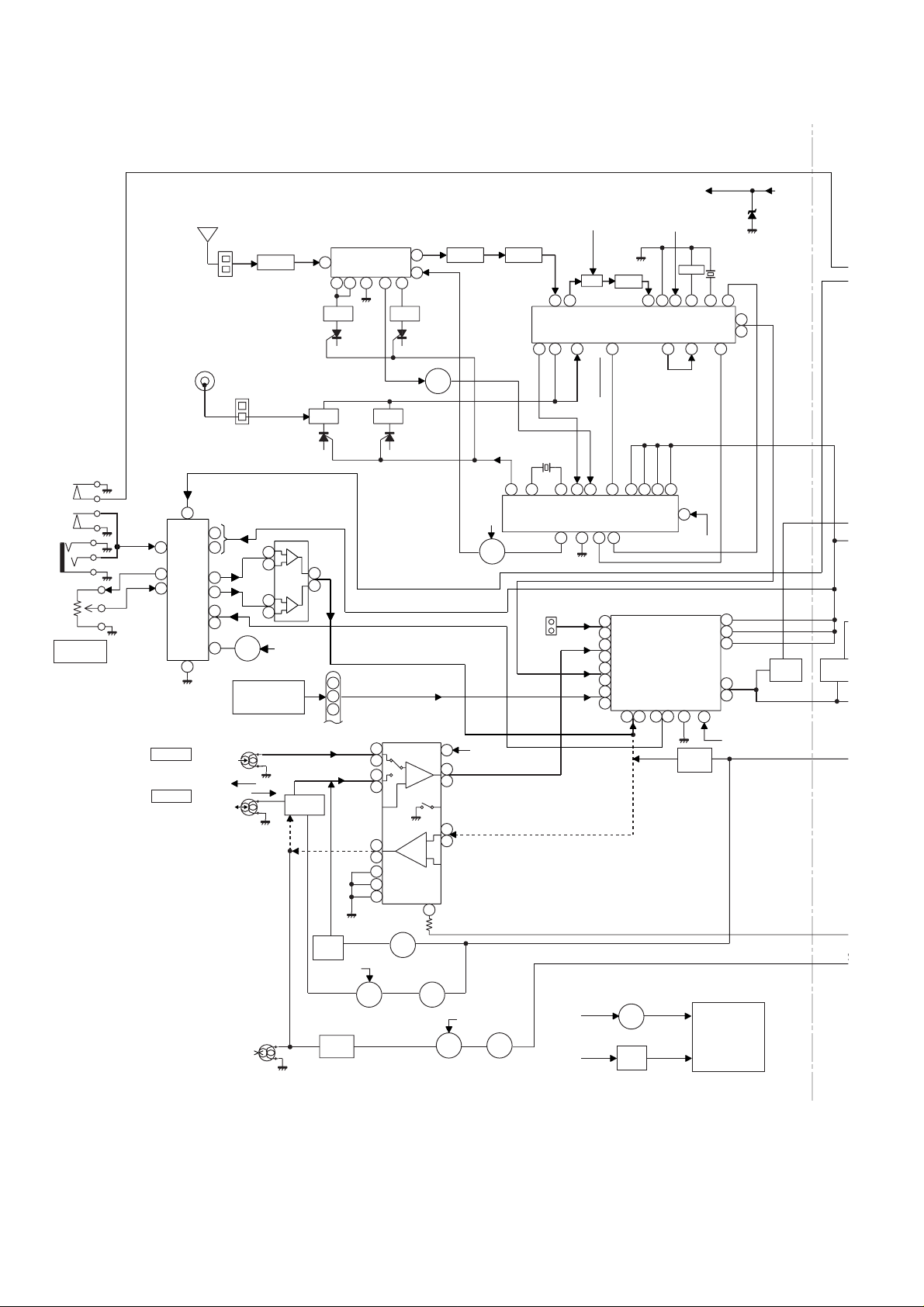
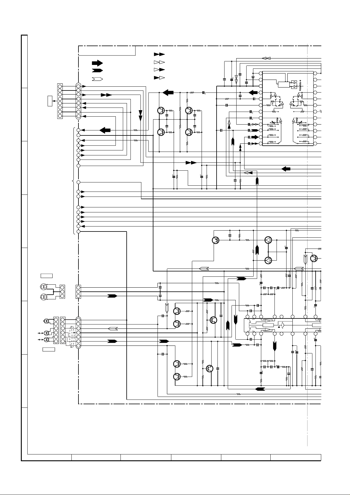
Figure 16 BLOCK DIAGRAM (2/3)
– 16 –
Page 17
+B5
51
Q705
CD-XP205V
FL701
FL DISPLAY
~
32
27
33
13
12
~
14
+B9
~
19
~
45
41
+B10
TO CD
SECTION
TAPE
MECHANISM
ASS'Y
601
602
REC/PLAY
Q603
Q604
T1/T2
BIAS
MUTE
SYSTEM
VF1
STK4029S
POWER AMP.
1
L
15
R
13
+B3
+B4
+B5
VF2
–VF
+B7
+B8
+B9
UNSW_5.6V
+B10
5655
70
~
78
79
VLOAD
80
~
85
86
~
91
92
93
VDD
100
12456 78
+B10
SP DET.
IC901
L-OUT
7
10
R-OUT
9
8
-B2
+B2
IC855
VOLTAGE
REGULATOR
KIA7810AP
KIA7805AP
IC854
AN78L05
IC853, IC854
KIA7812AP
IC851
IC852
IC853
M_13V
LD+7V
A_10V
D_5V
A_5V
SW_5V
VOLTAGE REGULATOR
505549
5438 5251
46
48
VDD
IC701
IX0560AW
SYSTEM
MICROCOMPUTER
RESET
VDD
1 0 16 1 7 20 212223 24
1112
XL700
4.194304 MHz
RESET
Q709
Q901~
Q904
T4A L 250V
D802
T4A L 250V
IC851, IC852
VOLTAGE
REGULATOR
D803, D804
~
+B10
+B10
SP RELAY
ON-OFF
F802
F801
T2A L 250V
F804
T2A L 250V
VOLTAGE
REGULATOR
Q801
F803
40 25 13
AVDD
CLK
CEDIDO
FAN MOTOR
Q905
RL914
TRANSFORMER
39
+B10
34
33
~
31
9
37
29
26
15
41
DRIVER
PT801
POWER
RX701
REMOTE
1
SENSOR
2
KEY
SW701-SW707
SW711-SW725
SW727-SW729
TO CD
SECTION
Q906
+B3
HEADPHONES
T.F.
3
+B10
SW601
SPAN
SELECTOR
+B7
M4
M
FAN
MOTOR
SO901
SPEAKER
TERMINAL
JK701
230-240V
127V
110V
220V
AC 110/127/220/230-240 V,
50/60 Hz
SW801
VOLTAGE
SELECTOR
SUPPLY CORD
AC POWER
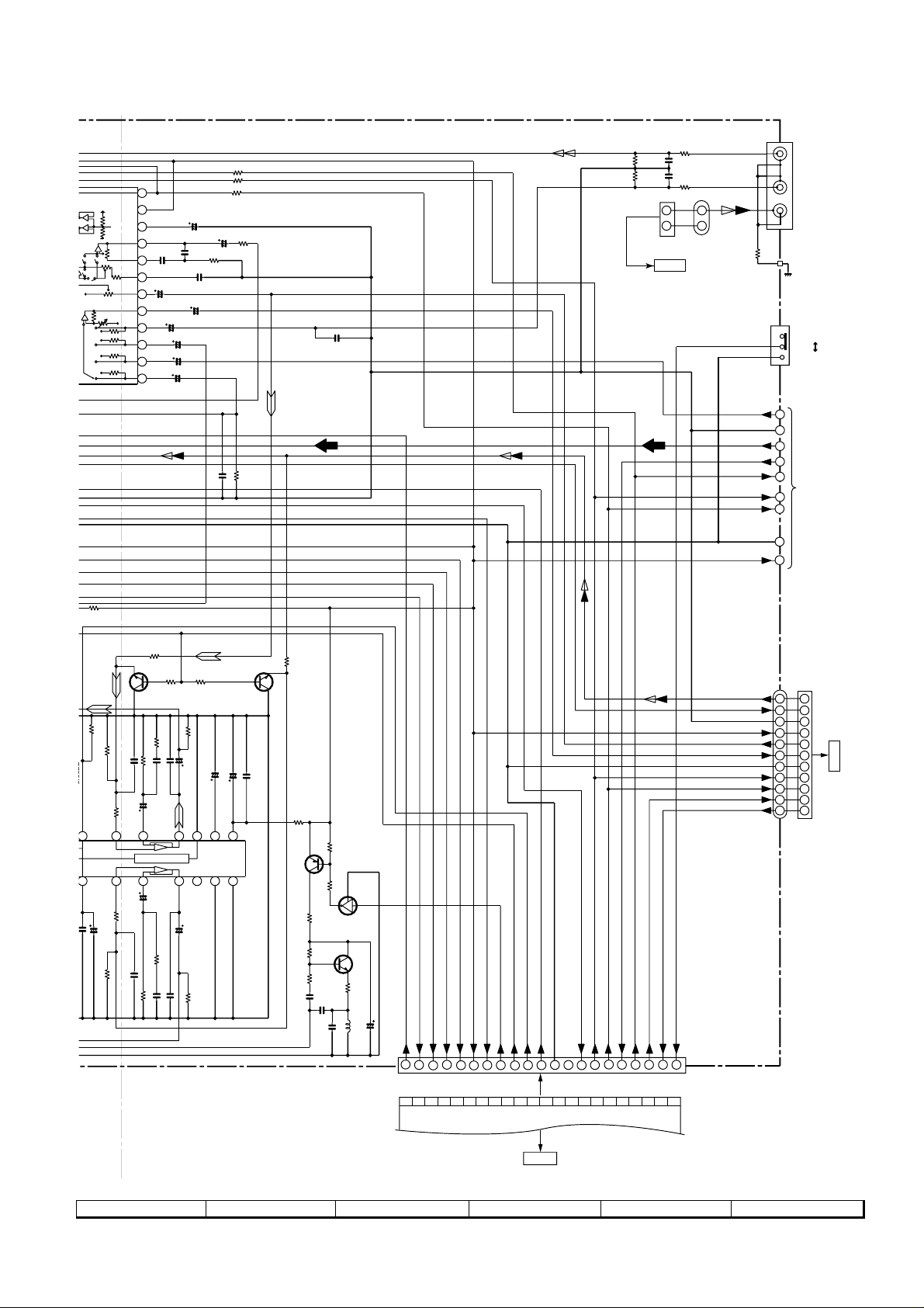
Figure 17 BLOCK DIAGRAM (3/3)
– 17 –
Page 18
CD-XP205V
+
–
C
T
1
1
3
0
/
0 022
100
/
0 022
C
1
A
B
C
D
E
F
G
P27 12 - D
TAPE 1
PLAYBACK HEAD
R-CH
L-CH
ERASE
HEAD
R-CH
L-CH
TAPE 2
RECORD/
PLAYBACK HEAD
CNS601
R-CH
1
A_GND
2
L-CH
3
CD_GND
4
D_5V
5
CNP11
A-5V
6
D_GND
7
LD+7V
8
TO VIDEO CD SERVO PWB
11
10
13
16
15
P22 1 - E~H
TO POWER SECTION
12
14
17
1
1
T1_R
2
2
A_GND
3
T1_L
3
1
1
2
2
3
4
5
6
3
4
5
6
CNS102
2
MAIN PWB-A1 (1/3)
FM SIGNAL
PLAYBACK SIGNAL
BI601
1
2
3
4
5
6
7
8
L-CH
1
GND
(A_GND)
2
R_CH
3
LD+7V
7
A_5V
D_5V
GND(CD_GND)
CD(A_GND)
GND(D_GND)
+B_PROTECT
9
M_+13.5V
6
A_+10V
8
SW_5V
UNSW_5.6V
SP_DET
5
SP_RLY
4
GND(M_GND)
CNP101
M_GND
1
ERASE
T2_R2
3
A_GND
4
T2_R1
5
T2_L1
6
T2_L2
7
BI102
RECORD SIGNAL
+B
+B
CD SIGNAL
VIDEO SIGNAL
VIDEO OUT SIGNAL
C609
C635
C636
1/50
0.001
0.001
R110
R109
0V
4.7K
4.7K
R621
9.3V
9.3V
0V
0V
R107
22K
47K
C602
0.022
R607
3.9K
C611
0.0022
C629
0.001
KTA1266 GR
SWITCHING
R102
1K
R101
1K
47K
R108
0V
0V
Q106
Q105
SWITCHING
KTC3199 GR
0V
0.0022
C136
8.6V
Q112
C106
SWITCHING
KTC3199 GR
560P
C105
MIC SIGNAL
Q603, Q604: SYSTEM MUTE
+B
+B
R619
330
R618
330
+B
+B
Q603
KTC3199 GR
C638
Q604
KTC3199 GR
C102
560P
C101
560P
C104
180P
C103
180P
R617
2.2K
C637
0.001
R616
2.2K
C640
22/50
SWITCHING
KTC3200 GR
0V
KTC3200 GR
SWITCHING
KTC3200 GR
SWITCHING
R615
0.001
R614
Q102
0V
0V
Q104
SWITCHING
KTC3200 GR
0V
0V
0V
Q101
4.7K
4.7K
R620
22K
Q103
0.7V
0.7V
0.7V
0.7V
Q601
Q602
R105
3.3K
R103
2.2K
R106
R605
10K
R613
390
R611
2.2K
KTC3199 GR
R610
2.2K
KTC3199 GR
R612
390
C639
1/50
S_MUTE
R104
2.2K
3.3K
C625
560P
C601
0.022
220P
C653
220/16
220P
C652
C607
0.1
C613
1/50
C615
4.7/50
C617
1/50
C619
1/50
C621
1/50
C623
1/50
R609
1.2K
R147
10K
10K
R146
R148
4.7K
R112
15K
R114
1K
R
C108
330P
24 23 22
1 2 3 4 5
L
C107
330P
R113
1K
R111
15K
1
DI
220P
C651
CE
2
VSS
3
LOUT
4
LBASS
5
C605
LTRE
0.1
6
LIN
7
LSEL0
8
L4
9
L3
10
L2
11
L1
12
AUDIO PROCESSOR
SWITCHING
Q113
L
KRC104 M
3.4V
0V
23
1
0V
1
3.4V
0V
23
R116
56
C112
100/25
C114
C116
0.033
C110
330P
C109
330P
C113
0.033
C111
100/25
R115
56
100K
R118
–
+
112K
Hich=T1
112K
+
–
100K
R117
R120
R119
C115
3.9K
560P
CCB
INTERFACE
+
–
+
–
+
–
AUX
DECK
TUNER
IC601
LC75341
C141
100/16
Q114
KRC104 M
R122
10K
R124
560P
5.6K
C118
47/25
2021
C121
0.022
3.9K
R123
C117
47/25
R121
10K
CLK
VDD
–
+
VREF
+
–
ROUT
+
–
RBASS
+
–
RTRE
RIN
RSEL0
+
–
CD
–20dBATT
R
R149
150
0V
SWITCHING
C120
5.6K
0V
68K
R150
R126 4.7K
0.0022
R128
5.6K
IC101
6 7 8
R129
5.6K
C143
3.3/50
C123
C119
0.0022
4.7K
R127
24
23
22
21
20
19
18
17
C6
1/5
R4
16
R3
15
R2
14
R1
13
R1
22
0.7
Q
KTC3
MU
R132
C128
C124 270P
R130 1.5K
C1
22
171819
Hich=
+
–
C1
22
R133
270P
C127
1.5K
R131
H
• NOTES ON SCHEMATIC DIAGRAM can be found on page 39.
1
23456
Figure 18 SCHEMATIC DIAGRAM (1/13)
– 18 –
Page 19
CD-XP205V
+
0.0022
C119
JK690
1
CLK
VIDEO/AUX
L-CH
AUX IN
R-CH
VIDEO OUT
CHASSIS
50 kHz/9 kHz
100 kHz/10 kHz
SW601
SPAN
SELECTOR
26
2
27
DO
22
CE
25
DI
24
23
P21 10, 11 - H
TO TUNER SECTION
15
8
R693
33K
C691
R691
6.8K
R690
6.8K
390P
R692
C690
33K
390P
CNS602B
1
2
CNP2
P29 12 - C
TO
VIDEO CD PWB
1
2
BI602B
R694
TUN_R
A GND
TUN_L
D_GND
A_+10V
KOK OUT(R)
KOK IN(R)
KOK OUT(L)
KOK IN(L)
+B
+B
+B
+B
+B
R601 1K
22/50
C620
1/50
C622
1/50
C624
1/50
C603
C608
0.1
4.7/50
R602 1K
R603 1K
C610
1/50
C612
0.0022
C616
C626
R606
3.9K
0.0022
R604
10K
R608
1.2K
C630
0.001
24
CLK
VDD
–
+
+
–
–
+
–
1
ESSOR
–20dBATT
23
+B
VREF
22
ROUT
21
+
–
RBASS
20
C606
RTRE
0.1
19
RIN
18
C614
RSEL0
1/50
17
C618
1/50
R4
16
R3
15
R2
14
R1
13
R149
150
R136
220K
0V
R138
10K
0.7V
Q108
0V
KTC3199 GR
MUTING
R126 4.7K
C124 270P
Hich=CHROME
R129
5.6K
3.3/50
270P
C123
4.7K
R132
C128
R130 1.5K
C126
22/50
171819 13141516
–
+
+
–
C125
22/50
R133
C127
0.022
1.5K
R131
68K
R150
R128
5.6K
IC101
6 7 8
C143
0.0022
R127
R139
100
C130 0.0033
0.022
C132
56K
56K
9
C131
47/25
100
R135
C129 0.0033
10K
Q107
KTC3199 GR
MUTING
10K
R134
47/25
C133 22/50
C134 220/10
RIPPLE
Nor/CrO2
ALC
ALC
10 11 12
10K
REC_R
0.7V
C135 0.022
VCC
GND
IC101
REC_L
R137
220K
0V
R158
220
11.7V
11.6V
Q109
0V
SWITCHING
KTA1266 GR
R141
4.7K
11.6V
R142
82(1/2W)
47K
R143
AN7345K
PLAYBACK AND RECORD/
0V
R144
22K
PLAYBACK AMP.
C138
0.0082(PP)
C137
0.047(ML)
C139
0.039(ML)
R140
47K
1
0V
23
0V
Q110
KRC104 M
BIAS
0V
Q111
0V
R145
4.7
L103
330µH
T-T1 T2
REC/PLAY
T_BIAS
BIAS OSC
KTC3203 Y
C140
47/25
1
–20dB
SP_DET
SP_RLY
2
345
+B
SW_5V
UNSW5.6V
+B
A_+10V
A+10V
6
T_BIAS
M_+13.5V
8
7
DI
CLK
D_GND
LVL_DET
CLK
DI
+B-PROTECT
D_GND
S_MUTE
T_T1/T2
REC/PLAY
11 12 13 14 15 16 17 18 19 20 21
10
9
DO
DO
CE
CE
KOK_LATCH
MIC IN
SPAN
CNP601
KOK OUT(L)
KOK IN(L)
A_GND
A_+10V
KOK OUT(R)
KOK IN(R)
D_GND
CLK
KOK_LATCH
MIC IN
BI602
CNS602
1
1
2
2
3
3
4
4
5
5
6
6
7
DI
8
9
10
11
CNPK1
7
P30 6 - C
8
9
10
11
TO MIC PWB
1
FFC701
CNP701
P24 1 - F
TO DISPLAY PWB
7
8 9 10 11 12
21
Figure 19 SCHEMATIC DIAGRAM (2/13)
– 19 –
Page 20
CD-XP205V
7
0
0
C351 0 022
A
B
C
AM LOOP
ANTENNA
D
SO302
FM ANTENNA
TERMINAL
E
F
C302
0.001
AM TRACKING
AM ANTENNA
C323
C338
0.001
D301
DS1SS133
D302
DS1SS133
BF301
B.P.F
1 2 3
C303
CNP302
121
2
10P(CH)
1 2 3 4
C304
0.01
C308
D305
4.7P(CH)
DS1SS133
C314
0.0047
0.022
AM BAND
COVERAGE fL
IC301
TA7358AP
FM FRONT END
6
5
C305
4.7P(CH)
C320
0.001
C309
0.001
VD302
R311
22
C316
100K
0.022
SVC211C
33K
R313
C317
0.001
FM RF
C315
0.0047
L312
R314
AM OSC.
T306
8
9
7
R302
10
C306
C311
18P
FM OSC.
C310
T301
15P(CH)
FM BAND
COVERAGE fL
C312
0.022
R325
47K
R327
33
T303
C335
560P
C334
0.022
C324
4.7P(UJ)
T302
FM IF
R322
680
C318
100P
Q302
KTC3194 Y
OSC BUFF
22P(UJ)
C307
10/50
VD303
SVC211C
C313
22P
(CH)
FM SIGNAL
AM SIGNAL
CF303
1
C331
0.047
C332
C330
0.022
15P(UJ)
VD301
SVC348S
68K
R323
R309
10K
3
2
+B
R316
4.7K
R336
10K
TP301
+B
C342
0.022
+B
+B
C3
0.
+B
R382
C381
12P(CH)
X352
4.5 MHz
C382
15P(CH)
C383
56P
150
R3
47
G
H
• NOTES ON SCHEMATIC DIAGRAM can be found on page 39.
1
23456
Figure 20 SCHEMATIC DIAGRAM (3/13)
– 20 –
+B
Page 21
+B
TP301
+B
C342
0.022
R382
C381
12P(CH)
X352
4.5 MHz
C382
15P(CH)
+B
+B
150
C397
0.022
R365
10K
R358
3.9K
24
5.6K
R351
AM OSC OUT
FM IF IN
132
C351 0.022
C352 10/50
R381
10K
C389
20
22
21
VSS
AOUT
IC302
X OUT
X IN
1234
C361 0.022
C362 3.3/50
22
23
21
FM AFC
AM OSC IN
REG
AM MIX OUT
T351
AM IF
C350 0.022
+B
C392
C394
47/25
0.001
C380
10/50
1.5K
R380
1/50
18
19
AIN
DI
CL
CE
5
C363 0.022
20
AM RF IN
R352
1K
1
+B
2.2K
R379
16
17
PD
VDD
DO
FM/AM
6
7
C364 2.2/50
C366 0.001
C365 0.022
18
19
VSM
FM/AM OUT
AM LOW CUT
AM IF IN
GND SDSTEREO
4
5
3
2
CF352
C393
0.001
C387
0.022
L351
0.01
C385
14
15
AM IN
FM IN
IF
FM/AM
CONT
10
8
9
R350
6
C353
100µH
1213
SD
IF IN
MO/ST
11
2.7K
C367
1/50
0.022
ST IND
R393
47K
R377
C386
330P
R376
1K
7
C354
1K
TP302
FM DET
8
0.022
X351
456 kHz
17
270
R353
CF351
C399
1/50
C368
16
MPX VCO
VCC
9
0.022
C398
+B
R395
47K
R360
4.7K
470K
R357
1K
R356
MPX IN
IF OUT
10
11
C357
2.2/50
C356
0.001
R388
100/10
15
PHASE
3.9K
+B
C374
0.015
C369
27P(UJ)
14
R-CH OUT
R355
3.3K
22P
C355
5.6K
R387
C373
0.015
C371
1/50
C372
1/50
13
MO/ST
L-CH OUT
(FM/AM)
PHASE
12
C358
+B
R359
R361
10K
R362
10K
+B
IC303
LA1832S
1/50
1/50
C370
L352
100µH
C396
100/10
R392
270
SWITCHING
Q360
KTA1266 GR
+B
R385
5.6K
1.8K
5.6K
R384
8.2K
8.2K
R363
R364
FM IF DET./
FM MPX./AM IF
ZD351
DZ5.1BSB
C395
0.022
+B
R391
270
+B
R383
5.6K
C391
47/25
C388
0.001
CD-XP205V
MAIN PWB-A1 (2/3)
C383
56P
R375
470
R372 1K
R373 1K
R374 1K
R378 1K
IC302
LC72131
PLL (TUNER)
R386
22K
+B
+B
CEDICLK
DO
25 24 23 22
TO MAIN SECTION
7
8 9 10 11 12
C384
0.001
+B
A_GND
A_10V
2
8
P19 12 - C, D
TUN_R
D_GND
15 26 27
TUN_L
Figure 21 SCHEMATIC DIAGRAM (4/13)
– 21 –
Page 22

CD-XP205V
18V
13V
3
1
3 1
3 1
3 1
2
2
2
2
+B_PROTECT
GND (D_GND)
GND (M_GND)
+B2
R-CH
L-CH
SP_RLY
SP_DET
GND
(CD_GND)
CD(A_GND)
A_+10V
M_+13.5V
L
R
R
L
L
R
FAN MOTOR 5V
UNSW_5.6V
D_5V
SW_5V
LD+7V
A_5V
(A_GND)
GND
5
4
3
2
1
4
5
2
3
1
15
1413121110
9 8 7 6
5 4 3 2 1
1
2
3
4
5
1
2
3
4
5
CH1
OUT
OUT
CH2
CH2
CH1
–
–
+
+
+VCC
–VCC
R-CH
L-CH
CNS705
P25 12 - E
FROM DISPLAY PWB
P18 1 - B~D
TO MAIN SECTION
1
2
3
4
5
6
7
8
9
10
11
12
13
14
15
16
17
SP R
ON-
VOLTAGE REGULATOR
+B
+B
+B
+B +B
+B
+B
-B
-B
-B
-B
-B
+B
+B
+B
+B
+B
+B
+B
+B
+B
+B
+B
+B
+B
+B
+B
+B
+B
-B
IC901
STK4029S
POWER AMP.
C907
820P
R903
1K
C905
3.3P
(CH)
C903
0.001
R907
56K
R909
1K
R911
820
C909
4.7/50
R901
56K
C901
0.22/50
R921
100(1/4W)
Fusible
C913
100/63
R925
22K
C932
0.22
R923
1K
R915
1.5K
C911
0.022
R913
0.1 (1W)
Q901
KTC3199 GR
D905
DS1SS133
C915
10/63
C916
10/63
R919
0.22(2W)
R917
0.22(2W)
R922
100(1/4W)
Fusible
C914
100/63
R920
0.22(2W)
R918
0.22(2W)
R912
820
C910
4.7/50
R904
1K
R910
1K
C908
820P
C906
3.3P(CH)
R908
56K
R914
0.1 (1W)
C912
0.022
R916
1.5K
R924
1K
D906
DS1SS133
Q902
KTC3199 GR
D907
DS1SS133
Q904
KTC3199 GR
Q903
KTC3199 GR
R936
56K
R935
56K
R937
56K
C925
47/50
C928
0.22
R940
4.7
R941
4.7
C929
0.22
R93
680
R943
680
D
DS1
Q9
KTC31
BI801
CNS801
C
CNP802
C856
3300/35
C855
0.1(ML)
IC852
KIA7810AP
C854
0.1(ML)
C853
47/25
R853
22K
D852
DS1SS133
D857
DS1SS133
R859
22K
C863
22/50
IC855
KTC2026
R860
220
C865
10/50
ZD852
DZ8.2BSB
D851
DS1SS133
C851
0.047(ML)
R854
22K
C852
22/50
D859
DS1SS133
IC851
KIA7812AP
R927
22K
C949
2200/63
C948
2200/63
R926
22K
C864
0.1(ML)
D858
DS1SS133
IC853
KIA7805AP
C859
0.1(ML)
C858
0.022
C857
47/25
R852
10K
IC854
AN78L05
IC851~IC854
VOLTAGE REGULATOR
C861
0.047(ML)
C860
47/25
D856
DS1SS133
C862
10/50
C904
0.001
R902
56K
C902
0.22/50
C926
0.22
C927
0.22
A
B
C
D
E
F
G
H
• NOTES ON SCHEMATIC DIAGRAM can be found on page 39.
1
23456
Figure 22 SCHEMATIC DIAGRAM (5/13)
– 22 –
Page 23

CD-XP205V
+
C927
0.22
C929
0.22
R941
FM SIGNAL
D912
C931
10/50
C930
47/50
R950
R949
1K
68K
M_+13.5V
SP_RLY
R-CH
GND
L-CH
HLD803
Q906
+B
DS1SS133
+B
680
680
D911
Q905
ON-OFF
R942
680
R939
680
RL914
R946
47K
R945
1.5K
R944
1.5K
R_OUT
L_OUT
R938
R943
L
R
DS1SS133
KTC3199 GR
SP RELAY
4.7
+B
R947
15K
+B
+B
+B
CNP971
2
1
DRIVER
KTC3203 Y
FAN MOTOR
1
5
+
+
–
–
SPEAKER
TERMINAL
CNS971
+
2
–
M
1
M4
FAN MOTOR
FW803
SP_L-CH
SP_R-CH
6 OHMS MIN
SP_L-CH_GND
SP_R-CH_GND
SO901
CNP705
+B
1
2
3
4
5
HEADPHONES
HEADPHONES
PWB-B2
JK701
MAIN PWB-A1 (3/3)
BI801
B2
CNS801
1
2
3
4
5
P25 12 - E
CNP801
VCC
1
1
GND
2
2
–VCC
3
3
4
4
5
5
CNP802
1
2
3
CNS705
4
5
FROM DISPLAY PWB
VF2
–VF
P_IN
VF1
R801
220K
12K
R803
R804
+B
-B
C801
R805
R802
47K
100/35
47
D3SBA60F
C802
47/50
ZD801
DZ6.2BSA
D802
C807 0.1(ML)
C806 0.1(ML)
ZD802
DZ6.2BSA
47K
R806
–28V
–33V
R807
10
REGULATOR
+B
47
C809
0.1(ML)
C808
0.1(ML)
-B
D803
RL204F
D804
RL204F
D805
ZD803
DZ300BSB
2.2K
(1/2W)
1N4004S
C804
220/63
C803
47/50
R808
–28V
Q801
KTA1274 Y
VOLTAGE
POWER PWB-A2
F802
T4A L 250V
F801
T4A L 250V
T2A L 250V
T2A L 250V
C805
22/100
D806
F803
F804
1N4004S
T.F.
PT801
POWER
TRANSFORMER
SW801
VOLTAGE
SELECTOR
230-240V
220V
127V
110V
K801
K802
TRANSFORMER PWB-A3
50/60 Hz
AC POWER
SUPPLY CORD
AC 110/127/220/230-240 V,
7
8 9 10 11 12
Figure 23 SCHEMATIC DIAGRAM (6/13)
– 23 –
Page 24

CD-XP205V
2
9
N
REMOCON
G9
D
G09
N
3
D
4
6
K
1
A
E
M
A
B
C
D
CNS702
6
6
5
5
4
4
3
3
CNP1
P29 12-B
2
2
TO VIDEO CD PWB
1
1
DISPLAY PWB-B1
BI702
ESS_ACK
6
ESS_STB
5
ESS_DI
4
ESS_DO
3
DSA_DATA
2
DSA_ACK
1
C706
47/25
R752
FL701
FL DISPLAY
R794
1.5
C707
1/50
33
R738
R755
4.7K
R772 10K
R770 10K
NP
F
F
P21
P20
P19
P18
P17
P16
P15
P14
P13
P12
R754
10K
R786
4.7K
P11
45 44 43 42 41 40 39 38 37 36 35 34 33 32 31 30 29 28 27 26 25 24 23 22 21 20 19 18 17 16 15 14 1
Q705
KTC3199 GR
R793
1K
R792
100K
47K
FOR PHILIPPINES
ONLY
D704
DS1SS133
D701
DS1SS133
R753 1K
P10
P09
P08
R745 1K
R744 1K
R743 1K
R742 1K
R784 1K
R785 1K
R741 1K
R746 1K
R734 1K
R735 1K
R732
1K
NXNXNXNXNXNXNX
P07
81 82 83 84 85 86 87 88 89 90 91 9
S11
S9
80
S12
S10
79
VLOAD
S13
78
77
S14
76
S15
S16
75
74
DIST3/S17
DIST2/S18
73
DIST1/S19
72
DIST0/S20
71
S21
70
DIST
69
STOP LED
68
REV_PLY_LED
67
FOR_PLY_LED
66
65
64
63
62
61
60
59
58
57
56
55
54
53
52
51
MICROCO
ILU_LED1
RDS READY/ESS DO
RDS RDCL/ESS DI
RDS RDDA/ESS STB
RDS RST/ESS ACK
MPEG POWER
DISC NO SW V_ONLY
KARAOKE LATCH
MIC SW
O/C_SW
JOG2
JOG1
VDD
AC_RLY
SP_RLY
50 49 48 47 46 45 44
P06
P05
P04
S6S7S8
IX0560
SYST
T_SOL_A
T_MOTOR
TIMER LED
43 42 41 40 3
P03
P02
1
IC70
52
T1 RU
51
T2 RU
SMUTE
T_SOL_B
P01
S1S2S3S4S5
VD
VSS
E
TO MAIN PWB
F
TAPE MECHANISM
PWB-F
PLAY
–
TAPE
M
MOTOR
SOLENOID
F. PLAY
SOLENOID
CASSETTE
+
G
P19 10 - H
CNP701
R729 560
R729 560
M_+13V
+B
R731 10K
R762
+B
R780
10K
+B
10K
FFC702
1
10
CNP701
21
20
19
18
17
16
15
14
13
12
11
10
9
8
7
6
5
4
3
2
1
CNP702
T2_PLAY SW
1
GND
2
T2 RUN
3
+MTR
4
SOL2
5
SOL1
6
F_REC
7
T1 RUN
8
9
10
SPAN
MIC IN
KARAOKE LATCH
CE
DO
CLK
DI
+B_PROTECT
LVL_DET
D_GND
S_MUTE
T_T1/T2
REC/PLAY
T_BIAS
M_+13V
A+10V
SW_5V
UNSW5.6V
SP_DET
SP_RLY
–20dB
R789 10K
R787 10K
C712
47/25
R788 10K
FPA/FPB
+B
MOTOR DRIVER
Q706
KTA1273 Y
+B
R777
R778
10K
R779
10K
10K
Q707
KTA1273 Y
Q708
KTA1273 Y
Q707, Q708: SOLENOID DRIVER
R774 10K
+B
D709
DS1SS133
D710
DS1SS133
R740
4.7K
R760
8.2K
21
1
FFC701
1
2
3
4
5
6
7
8
9
10
PH
R726 680
R727 680
R728 2.2K
R724 1K
R725 1K
R7
4.7
LE
SLR3
H
• NOTES ON SCHEMATIC DIAGRAM can be found on page 39.
1
23456
Figure 24 SCHEMATIC DIAGRAM (7/13)
– 24 –
Page 25

CD-XP205V
JOG2
/
NX
A
Y
NXNXNX
NX
P06
P05
P04
P03
P02
P01
G08
23 22 21 20 19 18 17 16 15 14 13 12 11 10
82 83 84 85 86 87 88 89 90 91 92 93 94 95 96 97
1
2
OAD
3
4
5
6
ST3/S17
ST2/S18
ST1/S19
ST0/S20
1
ST
OP LED
U_LED1
PEG POWER
SC NO SW V_ONLY
IC SW
C_SW
49 48 47 46 45 44
S6S7S8
S9
S10
V_PLY_LED
R_PLY_LED
MICROCOMPUTER
S READY/ESS DO
S RDCL/ESS DI
S RDDA/ESS STB
S RST/ESS ACK
RAOKE LATCH
JOG1
TIMER LED
VDD
AC_RLY
SP_RLY
R729 560
R728 2.2K
R729 560
R731 10K
10K
R762
G09
S1S2S3S4S5
G9G8G7G6G5G4G3G2G1
1
VDD
IC701
IX0560AW
SYSTEM
52
T1 RUN
51
T2 RUN
REMOCON
VSS
SMUTE
T_SOL_A
T_MOTOR
T_SOL_B
43 42 41 40 39 38 37 36 35 34 33 32 31
R724 1K
R733 1K
R726 680
R727 680
R725 1K
G04
G05
G06
G07
98765432
–20dBATT
SUB-CE/DSA_STB
REC/PLAY
CD RESOUT
T2_PLAY SW/
28
FPA/FPB SW
29
PROTECT
30
LVL_DET
DISC_NO SW/
DSA DATA
CD CLAMP SW
P_IN
AVREF
SP DET
R736 1K
R721 1K
G03
T_T1/T2
CD CLK
CD DO
TUN SM
DSA_ACK
AVDD
KEY 0
R720 1K
G02
100
99 98
T-BIAS
WRQ
SPAN
RESET
X2
X1
VPP/IC
XT2
DRF
VDD
CD DI
CD CE
CE
CLK
DO
AVSS
KEY 1
R719 1K
G01
1
2
3
4
5
6
7
8
9
10
11
12
13
14
15
16
17
18
19
20
21
22
DI
23
24
25
26
27
28
29
30
KEY 2
R718 1K
NP
F
1
C703
0.022
R763 1K
R701 100
R702 1K
R703 1K
R704 1K
R705 1K
R706 1K
R707 1K
R708 1K
XL700
4.194304 MHz
R769 1K
R709 1K
R710 1K
R711 1K
R712 1K
R713 1K
R714 1K
R715 1K
R716 1K
R717 100
R737 100
R739
1K
C720
0.022
R722 1K
C701
1/50
C702
1000/6.3
C704
15P
C705
18P
R759
5.6K
R795
1.5
+B
C721
0.022
R791 4.7K
R771 10K
4.7K
R747
R748
10K
MPEG_POWER
DSA_STB
DISC_NO SW
O/C_SW
CLAMP SW
RES OUT
CD CLK
CD DI
CD DO
CD CE
DRF
WRQ(DSP)
AC_RLY CON
P_IN
BI701
CNS701
121112
11
10
10
9
9
8
8
7
7
CNP12
6
6
5
4
3
2
1
BI705
VF2
1
–VF
2
3
VF1
4
5
5
4
3
2
1
1
2
3
4
5
CNS705
P27 12 - F
TO VIDEO CD PWB
CNP802
P23 7 - G
TO POWER PWB
D712
C714
3.3/50
DS1SS133
RD25
SW727
DIGEST
RD16
3.9K
SW717
REC
PAUSE
RD06
2.7K
SW706
REVERSE
PLAY
3.9K
+B
R782
100K
DS1SS133
RX701
REMOTE
SENSOR
1 2 3
SW728
RD17
5.6K
SW718
MEMORY/
SET
SW707
REVERSE
MODE
OSD
C716
RD26
0.022
5.6K
+B
+B
R783
100
+B
C717
47/25
SW729
P.B.C
RD18
10K
SW719
TUNING/
TIME DOWN
D711
SW720
CLOCK
DS1SS133
R773
10K
5V BACK UP
+B
RD19
680
SW721
VOLUME
UP
SW701
ON/
STAND-BY
R761
10K
R756
4.7K
R768
10K
R767
10K
R766
10K
+B
KEY 2
KEY 1
KEY 0
+B
+B
+B
R780
10K
+B
R
R765
4.7K
LED701
SLR342VCJ
RD20
820
SW722
VOLUME
DOWN
RD10
680
SW711CDSW712
RD01
680
SW702
FAST REWIND/
PRESET DOWN
+B
SW723
RD11
820
TUNER
(BAND)
+B
DISC
SKIP
RD02
RD21
1K
SW724
OPEN/
CLOSE
RD12
1K
SW713
TAPE
RD03
820
SW703
FAST FORWARD/
PRESET UP
L701
100µH
RD22
1.5K
SW714
VIDEO/
AUX
1K
C715
RD13
1.5K
R781
47K
0.01
UN_SW5V
D713
DS1SS133
RESET
Q709
KRC102 M
213
RD23
2.2K
SW725
EQUALIZER
X-BASS/DEMO
RD14
2.2K
SW715
TIMER/
SLEEP
RD04
1.5K
SW704
STOP
DS1SS133
RD24
2.7K
SW716
TUNING/
TIME UP
RD05
2.2K
SW705
PLAY
D714
RD15
2.7K
D715
7
8 9 10 11 12
Figure 25 SCHEMATIC DIAGRAM (8/13)
– 25 –
Page 26

CD-XP205V
H
R
6
C
0
R
A
PICKUP UNIT
B
C
D
VIDEO CD PWB-C (1/2)
CD SIGNAL
CNS1A CNS1B
Vcc
7
Vref
6
6
E
5
5
A
4
4
B
3
3
F
2
2
C
1
1
7
77
6
6
R51 10K
5
5
R52 1.8K
4
4
R53 1.8K
3
3
R54 10K
2
2
1
CNP9
R30
R31
220
1
Q6
R27
10K
1.2K
Q5
KTC3875 GR
KTC3875 GR
R26
10K
R33
1.2K
R32
220
Q7
KTC3875 GR
Q8
KTC3875 GR
R29
10K
C51
C53
47/6.3
0.001
R47
Q3
KTA1504 GR
LASER DRIVER
10
R37 5.6K
R43 5.6K
R41 5.6K
R36 5.6K
R56
1.8K
C54
47/10
R28
10K
R55
1.8K
+B
R25
10K
C55
0.01
C6
100/10
C8
0.1
C7
0.022
TIN1
FIN1
FIN2
TIN2
REF1
VREF
LDD
GND
LDON
AGON
EFBL
TEST0
TES1
R50
47
C23
R12
0.047
680
C17
C25
0.022
R79 1.5M
C24 0.22/50
C21
0.1
C22
100P
R11
(CH)
R8
330
C42
68P
(CH)
C28
47/10
13
R15
10K
C26
0.047
C29
0.022
12K
R80
1M
1
C27
0.1
P
2
R44
1K
R10
27K
EFBL
FIN1
FIN2
TIN1
TIN2
1
2
3
4
5
6
7
8
9
10
11
12
13
14
15
REF
REF
REF
REF
APC
ODRV
AGCON
IC1
LA9235M
SERVO AMP.
REF
ODRV
PH/BH
REF
REF
REF
REF
LPF
REF
REF
AGCON
PH
DH
REF
LPF
REF
LPF
REF
ODRV
REF
VCC
30
RFSW
29
RF–
28
27
26
25
24
23
22
21
20
19
18
17
16
RF
PH
BH
RFEV
FE–
FE
TE–
TE
HFL
TEST
R42
56K
5
C13 0.01
C89 560P
47/6.3
0.022
R7
6.8K
R5
68K
C14 0.33
R3 56K
R4 10K
C11
C12
C18
5P
(CH)
R6
47K
4
C20 0.1
0.0047
C82
0.022
C52
E
CNS2A CNS2B
1
TR+
FO+
FO–
TR–
F
ACTUATOR
G
CD MOTOR
PWB-D
M1
SPINDLE
M
MOTOR
M2
SLED
M
MOTOR
SW4
PICKUP IN
1
2
2
3
3
4
4
5
5
6
6
7
7
GND
+
–
+
–
8
CNS3A CNS3B
6
5
4
3
2
1
CNP3A
8
6
5
4
3
2
1
TR–
1
1
TR+
2
2
FO+
3
3
FO–
4
4
GND
5
5
PD
6
6
VR
7
7
LD
8
8
CNP10
SP+
6
6
SP–
5
5
SL+
4
4
SL–
3
3
PUIN
2
2
GND(D)
1
1
CNP3
0.01
C19
0.022
+B
100/10
+B
R24
TDO
FDO
C46
0.022
SLDO
R48
6.8K
C49
100/10
C50
1
2
3
4
5
6
7
8
9
10
11
12
13
14
15
16
17
18
19
20
21
–
–
+
+
–
+
–
+
IC3
M63001FP
FOCUS/
TRACKING/
SPIN/
SLED DRIVER
–
–
+
+
+
–
++-
+
-
–
–
+
+
+
–
+
–
+
–
1(1/2W)
42
41
+B
40
39
38
37
36
35
34
33
32
31
30
29
28
27
26
25
24
23
22
SPDO
C47
100/10
+B
+B
+B
C90
100/10
+B
+B
H
• NOTES ON SCHEMATIC DIAGRAM can be found on page 39.
1
23456
Figure 26 SCHEMATIC DIAGRAM (9/13)
– 26 –
Page 27

CD-XP205V
.
C71
100P(CH)
R68
1K
R67 1K
CONT7
CONT6
V/*P
GENERAL
SERVO
PROCESSEROR
GENERAL
CONT3
CONT2
CONT1
R40 1.2K
R45 1.2K
Q2
UN2211
1
2
C72 0.01
C73
100P(CH)
C76
100P(CH)
C78
3
100P(CH)
C80 0.1
VSS
VDD5V
73 72 71 70 69 68 67 66 65
LC78636E
SERVO/SIGNAL
CONTROL
ERROR
CORRECT
CONT5
CONT4
33 34 35 36
C2F
PCK
VDD
R46 1K
3
DRF
RES
IC2
AUDIO
OUT
DOUT
FSX
37 38 39 40
9
C30 0.022
C31 100/10
DI
DO
WRQ
COMMAND
INTERFACE
SUBCODE
DECODE
CRC
OUT
SERIAL
AUDIOIN
EXTERNAL
INTERPOLATION
MUTE
ATTENUATION
DEEMPHASIS
FILTER
DIGITAL
1BIT
DAC
EFLG
TEST
CE
CL
CLOCK
GENERATOR
LPF
EMPH
DISC-NO
R58 10K
R57 10K
+B
EFMO
PLL
VCEC
SLICE
LEVEL
CONTROL
+
–
25
CONTROL
S/HD/A
26
80 79 78 77 76 75 74
FSEQ
DEFECT
FRAMESYNC
DEFECT,PROTECT
EFMDECODE
CLV
CONTROL
JITER
DEFECT
SW
AUTO
ADJUST
A/DSW
FG(D_Vref)
LASER
27 28 29 30 31 32
SLDOSPDO
C23
R12
C21
0.1
680
R44
1K
R13
680
C81
0.022
R14
1.2K
C27
0.1
PH(RFENV)
ADAVDD
PCKIST
VVDD
SLCIST
SLCO
EFMIN
JITTV
JITTC
VREF
ADAVSS
PHREF
BHREF
TBLO
TDO
FDO
1
7
PD01
1
8
PD02
2
VVSS
3
4
5
FR
6
HFL
7
8
9
10
11
12
BH
13
14
FE
15
TE
16
17
18
19
20
21
22
23
24
0.047
R79 1.5M
C24 0.22/50
C22
25
100P
022
R10
27K
0.1
330
7
C42
47
68P
(CH)
2
EFBL
R11
(CH)
12K
R80
1M
R15
R8
10K
C26
0.047
C29
C28
0.022
47/10
2
13
6
R35
1K
R38
R39
270
470
R24
1(1/2W)
100/10
C47
+B
+B
+B
R22
R21
820
820
D21
KDS193
C90
100/10
+B
+B
D22
KDS193
64
63
62
61
60
59
58
57
56
55
54
53
52
XOUT
51
50
49
48
47
46
45
44
43
42
41
0.82 µH
SBCK
PW
SBSY
SFSY
16M
DATA
DATACK
LRSY
ASDFIN
ASDACK
ASLRCK
XVSS
R20 220
XIN
XVDD
RVDD
RCHO
RVSS
LVSS
LCHO
LVDD
MUTER
MUTEL
L61
OUTIN
C93
0.022
R71 1K
R72 1K
R73 1K
R75 100
R76 1K
R77 1K
R78 1K
L62
2.2 µH
12
10
10P(CH)
REGULATOR
SI3033LUS
3
C65
47/10
0.022
100/10
C85
8P(CH)
16.9344 MHz
C86
R19
2.2K
R9
22K
CE1
1/50
R2
2.2K
R17
1.5K
+B
VOLTAGE
Q4
2
GND
C44
C45
11
0.047
3.3(1/4)
GND(D)
XL2
C34
0.022
C84
R18
330
R1
330
R23
Fusible
1
C92
0.1
LD
LD
R59 33
R60 33
R61 33
C83
0.047
Q10
KTC3875 GR
Q9
KTC3875 GR
+B
M+
M–
+B
+B
+B
+B
+B
OPENNMP3O
DATA
DATACK
LRSY
+5V
+B
+B
+B
C87
1000/6.3
+B
R97
3.9K
WRQ
DRF
MPEG
POWER
DSA_STB
MPEG RESET
RAC/NTSC
RES
49
50
51
P28 1 - D, E
52
TO MPEG SECTION
CNP11
R-CH
1
2
AGND
L-CH
3
4
5
6
7
8
40
41
42
43
44
CNP12
1
2
CE
3
DO
4
DI
5
CL
6
7
8
9
10
11
12
45
46
47
48
CNP4
1
2
3
4
5
6
DGND
FROM MAIN PWB
+5V
A10V
DGND(OPTION)
+6.5V
R-CH
AGND
L-CH
A10V
P28 1 - E, P29 12 - A
D_GND
WRQ
DRF
CE
DO
DI
CLK
CDRES
CLAMP SW
O/C SW
DISCNO SW
DSA_STB
MPEG_POW
P28 1 - D, E
TO MPEG SECTION
CNS4
BI4
1
1
2
2
3
3
4
4
5
5
6
6
P18 1 - B
CNS601
TO MPEG SECTION
P25 12 - D
CNS701
FROM
DISPLAY PWB
SW1
OPEN/
CLOSE
SW2
CLAMP
SW3
DISC
+
NUMBER
M3
M
CD LOADING
–
MOTOR
CD
LOADING
MOTOR
PWB-E
• The numbers 1 to 13 are waveform numbers shown in page 41.
7
8 9 10 11 12
Figure 27 SCHEMATIC DIAGRAM (10/13)
– 27 –
Page 28

CD-XP205V
100
99
98
97
96
95
94
93
92
91
90
89
88
87
86
85
84
83
82
81
82
81
50
50
49
49
48
47
46
45
44
43
42
41
40
39
38
37
36
35
34
33
32
31
123456789
10 11 12
40 39 38 37 36 35 34 33 32 31 30 29
13 14 15 16 17 18 19 20
28 27 26 25 24 23 22 21
80 79 78 77 76 75 74 6667686970717273 65 525364 63 62 61 60 59 58 57 56 55 54 51
19 20 21 22 23 24 25 26 27 28 29 30
56789
10 11 12 13 14 15 16 17 18
4321
32 31 30 29 28 27 26 25 24 23
123456789
10
171819
202122
11 12 13 14 15 16
DBUS7
DA3
DA4
DA2
DA5
DBUS2
DBUS1
DBUS0
DBUS5
DBUS4
DA6
DBUS10
DA8
DA7
DA0
DBUS3
DBUS8
DBUS9
DBUS15
DBUS14
DBUS6
DA1
DBUS11
DBUS12
DBUS13
ADJ
VC
GND
OUT
IN
DSA_STB
MPEG
POWER
LD3
LD4
LD5
LD6
LD7
LA10
LA11
LA9
LA8
LA13
LA14
LA17
LD2
LD1
LD0
LA0
LA1
LA2
LA3
LA4
LA5
LA6
LA7
LA12
LA15
LA16
ARFS
RCLK
AJN
NTSC
RAC/
+5V
D_GND
DATACK
LRSY
DATA
P27 12 - C, E, G
TO CD SECTION
LROMCE#
PJM
VCC
A17
A14
A13
A8
A9
A11
OE_
A10
CE_
D7D6D5D4D3GND
D2D1D0A0A1A2A3A4A5A6A7
A12
A15
A16
VPP
CAS2_
OE_
RFSET#
VSS
D15
D14
D13
D12
VSS
D11
D10D9D8
CAS_A8A7A6A5A4VSSVCC
A3A2A1
A0
RAS_
WE_
VCC
D7D6D5
D4
D3D2D1
D0
VCC
DWE#
RAS#
GND
CAS#
TDMFS
100
99
TDMDR
TDMCLK
ARFS
ARCLK
AJN
DOE#
ATFG/SEL_PLL1
ATCLK
AOUT/SEL_PLL0
ACLK
LA17
LA16
LA15
LA14
LA13
LA12
VCC
GND
LA11
LA10
LA9
LA8
LA7
LA6
LA5
LA4
LA3
LA2
LA1
LA0
LCS0#
LCS1#
LOE#
LWR#
LD7
LD6
LD5
LD4
LD3
LD2
LD1
LD0
AUX7
AUX5
AUX6
VCC3
YUV0
GND
AUX4
AUX3
AUX2
AUX1
AUX0
PCLA
PCLA2X
CPUCLK
HSYNC
VSYNC
YUV7
YUV6
YUV5
YUV4
YUV3
YUV2
YUV1
VCC3
GND
DBUS15
DBUS14
DBUS13
DBUS12
DBUS11
DBUS10
32
31
DBUS9
DBUS8
DBUS7
DBUS6
DBUS5
DBUS4
DBUS3
DBUS2
DBUS1
DBUS0
MA8
MA7
MA6
MA5
MA4
MA3
MA2
MA1
MA0
VCC3
MPEG
RESET
123
5
4
13
2
46
52
48
45
49
47
44
50
51
+B
+B
+B
+B
+B
+B
+B
+B
+B
+B
+B
+B
+B
+B
+B
+B
+B
RM2
33
RM4
33
RM38
33
RM42 33
RM44 33
RM43 33
RM41
8.2K
CM35
0.022
CM34
10/16
CM28
0.022
CM27
10/16
CM26
0.022
ICM2
ES3880F
VIDEO CD DECODER
RM32
10
RM33
33
RM30 33
RM31 33
ICM4
IX0512AW
EPROM IC
CM39
0.1
RM82
2.2K
RM83
1.2K
RM36
330
CM38
47/10
RM34
10K
QM5
KTA1046 Y
QM3
UN2211
CM36
100/10
CM37
0.1
C91
0.1
QM6
SI3033LU
CM30
0.1
CM31 0.022
CM32 10/16
ICM1
1625635T
DRAM
CM29 0.022
CM40
0.01
CM33
0.022
CM56
33P
(CH)
RM45
4.7K
A
B
C
D
E
F
G
H
• NOTES ON SCHEMATIC DIAGRAM can be found on page 39.
1
23456
Figure 28 SCHEMATIC DIAGRAM (11/13)
– 28 –
Page 29

CD-XP205V
0
1
2
3
+
4
10K
CM48
100/10
RM61
RM60
10K
100/10
RM56
100K
CM43
10/16
RM70
220
RM71
3.3K
VCM
RSET
VREF
COMP
MIC1
AOL+
MIC2
AOL–
AOR–
AOR+
AVDD
VREFP
VREFM
AGND
AUX15
AUX14
AUX13
RSCK_SER_IN
AUX12
AUX11
AUX10
RSD/SPLL0
VCC
GND
N.C.
GND
RM16
4.7K
CM51
33P(CH)
CM49
33P(CH)
RM58
10K
QM1
KTC3265 Y
RM75
220
CM6
0.1
AGND
50
49
48
47
46
45
44
43
42
41
40
39
38
37
36
35
34
33
32
31
N.C.
+B
RM26
4.7K
RM64
15K
+B
RM59
10K
CM44
10/16
1000/6.3
RM72
+B
CM25
0.1
ARCLK
AJN
CM20
0.1
CM1
220
RM49
4.7K
CM52
10/16
CM53
10/16
RM67
100K
RM57
100K
CM3
0.1
CM23
0.1
CM22
10P(CH)
RM27
4.7K
+B
DSA_ACK
DSA_DATA
HSS_DO
HSS_DI
HSS_STB
HSS_ACK
RM76
15
CM4
0.1
CM24
100/10
CM21
100/10
RM65
RM73
2.2K
1K
RM66
RM68
100K
1K
CM54
22P(CH)
RM74
100
CM7
CM55
22P(CH)
100/16
RM15
4.7K
L_CH
A_GND
R-CH
A10V
VDAC
VGND
40
41
42
43
1
2
3
4
5
6
1
2
CNP2
CNP1
P27 12 - E
TO CD SECTION
CNS702
P24 2 - D
FROM DISPLAY PWB
CNS602B
P19 12 - B
FROM MAIN PWB
RM63
15K
IC6
TJM4558C
OPE AMP.
+B
RM1 33
RM3 33
RM5 33
RM6 33
RM7 33
RM8 33
RM78
4.7K
+B
CM13
0.001
LM3
0.82 µH
+B
33
33
LD7
32
33
3
LD6
LD5
+B
CM16
0.1
LD4
LD3
LD2
LD1
+B
CM12
27P(CH)
CM14
0.1
CM15
80 6768697071727378 77 76 75 7479 555657585960616263646566 51525354
22P(CH)
PCK2
DSC_D7
81
HSYNCt
82
DSC_D6
83
VSYNCt
84
DSC_D5
85
YUV7
86
YUV6
87
YUV5
88
YUV4
89
VDD
90
GND
91
YUV3
92
DSC_D4
93
YUV2
94
DSC_D3
95
YUV1
96
DSC_D2
97
YUV0
98
DSC_D1
99
GND
100
GND
12345
PCK
RM23
4.7K
CM17
VDD
0.1
CM11
GND
VCC
RM14
100K
XL1
27P(CH)
27 MHz
XIN
VDD
GND
DSC_D0
AUX00
DSC_C
6789
LD0
CM5
100/10
+B+B
RM80
1K
CM9
GND
XOUT
AUX03
AUX04
AUX05
AUX06
ICM3
ES3889F
VCD COMPANION
AUX07
RSTt
DCLK/EXT-CLK
AUX02
DSC_5
AUX01
10 11 12 13 14 15 16 17
CM18
0.1
RM52
RM51
10K
CM41
10/16
RM77
4.7K
RM9
150
RM12
150
RM13
150
0.1
VDD
VDAC
VGND
VGND
PLLCAP
TWS/SPLLOUT
AUX08
MCLK
VCC
MUTE
18 19 20 21 22 23 24 25 26 27 28 29 30
CM19
0.1
CM50
33P(CH)
RM62
CM46
33P(CH)
10K
RM53
CM42
10/16
+B
YDAC
VVDD
TSO
AUX09
10K
100K
RM11
150
CM47
0.1
RM54
100K
CM2
100/16
RM10
VVDD
CDAC
RWS/SPLL1
TSCK
ARFS
7
––
6
5
+
8
CM45
RM55
6.8K
+B
RM50
10
RM69
3.9K
+B
CM8
0.1
220
VGND
VGND
50
GND
RSTOUTt
IC6
RM81
1K
ACLK
AOUT
ATFG
ATCLK
VIDEO OUT SIGNAL
VIDEO CD PWB-C (2/2)
7
8 9 10 11 12
Figure 29 SCHEMATIC DIAGRAM (12/13)
– 29 –
Page 30

CD-XP205V
A
B
C
MIC PWB-G
DK1
DS1SS133
PINK1
DK2
DS1SS133
CK3
GND
0.001
CHASSIS
JK1
MIC
RK8 5.6K
CK54
0.1
CK41
100/16
CK1
0.01
RK4
10K
RK7
1K
RK3
56K
VRK1
20K(B)
MIC
VOLUME
+B
RK2
56K
CK7 0.47/50
CK8 4.7/50
CK9 2.2/50
CK10 0.1
CK11 0.1
CK13
0.0047
CK16 0.22
CK17 220/10
CK12
2.2/50
CK14
0.001
CK15
0.068
MIC SIGNAL
CK48
10K
ZDK1
MTZJ5.6B
RK13
1.2K
RK45
CK51
1/50
CK52
1/50
RK44
CK53
47/25
6.8K
6.8K
220P
RK46
18K
CK50
100P
CK49
100P
RK43
18K
CK47
220P
+B
CK44
47/25
RK47
RK49
QK1
KTC3203 Y
10K
CK43
47/25
RK50
8.2K
RK48
10K
RK12
100
ICK1
M65856SP
RK1
MIC AMP.
10K
MIC SW
1
MCLKC ONT
2
VACL
3
4
MIC1 IN
ALC1
5
MIC1NF IN
6
MIC1 OUT
7
MIC1 VOL IN
8
SOURCEOUT
MIC2 IN
9
ALC2
KEYCONIN
10
MIC2 NF IN
11
MIC2 OUT
12
MIC2 VOL IN
13
MICOUT
14
LPF1 IN1
15
LPF2 IN2
16
DAINTOUT
LPF1 OUT
17
AD INTOUT
18
AD INTIN
19
ADCONT
20
REF
21
DATA
CLOCK
LATCH
VCF IL
L OUT
R OUT
VOL IN
LPF2OUT
LPF2IN2
LPF2IN1
DAINTIN
DACONT
VCC
GND
R IN
PS2
PS1
L IN
42
41
40
39
38
37
36
35
34
33
32
31
30
29
28
27
26
25
24
23
22
RK10 1K
RK11 1K
RK9 1K
CK31 0.15
CK29 2.2/50
CK30 2.2/50
CK26 2.2/50
CK25 2.2/50
CK24 2.2/50
CK23 0.001
CK22 0.0047
CK21 0.068
CK20 0.22
CK18
100/16
CK35 47P
CK34 47P
CK33 47P
CK19
0.022
+B
+B
CK42
0.022
2
3
ICK2
5
6
RK14
100(1/2W)
RK15
100(1/2W)
KIA4558P
OPE AMP.
8
4
CK72
100/16
ICK2
1
CK46
2.2/50
CK45
2.2/50
7
CNPK1
1
2
3
4
5
6
7
8
9
10
11
CNS602
P19 12 - E
FROM MAIN PWB
RK42 10K
RK38
100
RK41 10K
RK37
RK39
1K
MIC OUT(L)
MIC IN(L)
390
A_GND
A_+10V
RK36
390
MIC OUT(R)
MIC IN(R)
RK40
1K
DATA
CLOCK
MIC LATCH
MIC IN
+B
D
• NOTES ON SCHEMATIC DIAGRAM can be found on page 39.
Figure 30 SCHEMATIC DIAGRAM (13/13)
E
F
JK1
MIC
G
VRK1
MIC
VOLUME
CK18
CK42
CK17
CK13
CK16
RK8
CK12
CK20
CK21
CK19
CK14
CK15
CK10
DK1
CK22
22
21
DK2
CK23
20
CK54
CK51
CK3
RK7
RK46
CK24
25
CK11
RK45
CK48
MIC PWB-G
H
15
CK9
CK50
CK7
4
3
2
1
30
CK25
ICK1
10
CK8
ICK2
CK46
5
6
7
8
CK26
35
CK52
RK43
RK47
RK48
CK29
5
RK2
RK3
CK45
RK49
RK44
CK49
CK47
RK50
CK72
CK31
40
RK4
CK1
RK38
RK37
QK1
E C B
ZDK1
42
1
CK53
CK43
CK30
CK41
RK12
RK13
RK36
RK1
RK41
RK15
RK14
CK44
RK40
RK42
CK35
RK11
RK39
CK34
RK10
11
10
9
8
7
6
5
4
3
2
1
CK33
RK9
CNPK1
PINK1
CNS602
P30 5 - A
FROM MAIN PWB
1
23456
Figure 30 WIRING SIDE OF P.W.BOARD (1/9)
– 30 –
Page 31

TRANSFORMER PWB-A3
SW801
VOLTAGE SELECTOR
AC POWER
SUPPLY CORD
AC 110/127/220/230-240 V,
50/60 Hz
CD-XP205V
COLOR TABLE
BROWN
BR
OR
YL
GR
BL
VL
GY
BK
PK
RED
ORANGE
YELLOW
GREEN
BLUE
VIOLET
GRAY
WHITE
BLACK
PINK
RD(R)
WH(W)
230-240 V
220 V
127 V110 V
BR
BL
K801 K802
230-240 V
220 V
127 V
110 V
T.F.
POWER PWB-A2
C805
D806
R808
R804
D805
R803
R805
ZD803
C801
C803
B C E
Q801
C804
FROM DISPLAY PWB
C802
R807
CNP802
12345
CNS705
P34 1 - E
ZD801
R806
T2A L 250V
D803
D804
C806
R801
F804
C807
ZD802
R802
T4A L 250V
C808
T2A L 250V
F801
C809
F803
D802
F802
T4A L 250V
CNP801
12345
CNS801
P33 7 - H
FROM MAIN PWB
PT801
POWER TRANSFORMER
7
8 9 10 11 12
Figure 31 WIRING SIDE OF P.W.BOARD (2/9)
– 31 –
Page 32

CD-XP205V
5
R607
5
6
C603
A
MAIN PWB-A1
CNS602
1110
BLGYBLGYBLGYBLGYBLGYRD
P30 5 - G
TO MIC PWB
CNPK1
987654321
B
C
D
E
F
G
VIDEO OUT
TO
VIDEO CD PWB
P36 1 - B
CNP2
FM ANTENNA
FM
75 OHMS
GND
JK690
VIDEO/AUX
R-CH
L-CH
CNS602B
R-CH
L-CH
L-CH
R-CH
SO901
SPEAKER
TERMINAL
SO302
TERMINAL
AM LOOP
ANTENNA
1
2
SW601
SPAN
SELECTOR
50 kHz/9 kHz
100 kHz/10 kHz
WH
1
BK
FAN MOTOR
BR
RD
CNS971
+
+
–
–
M4
C302
C382
C381
C397
C394
R381
C307
C306
9
8
7
R314
6
5
C338
C323
T303
R690
C690
BK
WH
C331
R692
R691
C691
1
R950
R947
IC301
C304
C303
123
BF301
C330
TP301
R693
R949
C931
D912
4
3
2
1
R620
E C B
Q906
C305
C640
B C E
R940
CNP302
1
2
D301
D302
R694
22
BI602B
GY
2
1
C384
R322
C315
C314
C317
VD301
R944
X352
C320
R325
R302
C310
C308
L312
R323
C332
C335
R616
Q604
C638
C930
R945
D911
LUG3
CNP971
E
C
B
R373
R374
123456789
IC302
R379
20
19
22
21
C392
C380
R380
C389
B C E
Q302
R327
C311
C312
T302
CF303
C309
VD302
D305
R313
C316
R316
C334
R336
C362
T306
Q602
B
R614
R604
R612
C
E
R618
1
2
R924
Q902
R946
Q905
C926
C928
18
C393
B
C
E
C910
R372
17
16
R377
L351
R375
T301
C324
R309
1 2 3
R311
R365
C636
R908
C387
15
14
C385
C318
C350
VD303
C342
R621
R610
C912
R916
R902
R904
RL914
R378
10
13
C313
C361
C363
C639
C902
R910
R936
R359
11
C386
R360
12
R384
R387
B
R393
C
Q360
E
R382
T351
3
2
CF352
1
C352
CF351
C353
R352
123456789
R351
22
21
20
24
23
IC303
C367
R358
R350
C365
C364
Q601
B C E
C635
R611
D906
C916
C904
R912
C908
C914
C906
R388
R376
R386
R385
C391
R383
C398
C354
10
C351
C399
C366
19
18
17
16
15
R615
R613
D907
R937
C915
R922
IC901
15 14 13 1211 10
C929
C927
R941
C383
C396
R391
R395
R392
ZD351
C356
C357
R353
R355
12
11
X351
13
14
C371
C369
R356
R357
C368
TP302
Q603
E C B
C637
R619
E
B
C
C
B
E
C925
Q903
Q904
C913
987654321
R914
R920
C395
C370
C355
C372
R921
R918
L352
C358
R361
R362
C374
R617
C373
R605
R925
R919
R363
R364
C932
C388
C901
R917
C909
R901
C903
R911
R907
C905
R903
C907
R909
R913
D905
R935
R927
R923
R915
E C B
Q901
R926
R602
R601
C911
C864
C852
123
IC851
C609
C601
C6
C651
C
R603
11
R8
C948
H
1
23456
Figure 32 WIRING SIDE OF P.W.BOARD (3/9)
– 32 –
Page 33

CD-XP205V
1
927
RD
E C B
R926
R923
R915
Q901
IC851
R602
C911
C864
R601
C852
C609
C601
C653
C651
C610
R603
R854
C948
1
C615
R607
C607
123456789
C652
C602
22
24
23
C608
C603
C614
BI602
D858
D859
C851
C855
IC852
P31 10 - H
TO POWER PWB
P35 12 - D
TO DISPLAY PWB
CNP701
C613
C605
C611
10
IC601
21
20
19
18
17
16
15
C622
C606
C612
C618
C630
C620
C616
R606
C853
C854
R853
123123123
R852
C858
R939
R943
CNP801
CNS801
C619
C629
C617
R609
C625
11 12
14 13
1
111
1113151719
10121416182120
CNP601
C857
GY
5
WH
4
GY
3
WH
2
RD
1
TO VIDEO CD PWB
C621
C623
C624
BI601
2468
IC853
C859
C949
FFC701
21
P36 1 - E
CNP11
12345678
RDBLWHBLWHBLWH
R608
C626
R127
R137
C119
R121
C117
R123
R119
R117
8
C113
CNP101
C101
Q114
13579
Q113
5
BI801
1
CNS601
BL
B
C
Q107
E
23
3 2 1
3 2 1
C125
R131
R129
C123
C143
C115
1
C102
R149
C127
R135
C121
C107
R101
Q105
R139
C111
R113
E
C
B
R110
R109
R148
R158
R138
C131
R133
Q106
R107
LUG4
C129
R115
C105
E
C
B
R147
C856
C134
12
11
10
9
8
7
6
5
4
3
2
1
C141
C136
Q110
C133
R102
R108
R146
Q108
R130
R134
C135
IC101
C108C109
7
R114
C106
E
C
B
3 2 1
B C E
C132
C130
R132
C128
C126
R126
13
14
R128
15
C124
16
R150
17
18
19
20
21
R118
22
23
24
C103
BI102
1
C138
C139
Q112
Q109
D851
C862
123
IC854
C112
R116
E C B
R111
E C B
E C B
E C B
Q104
C104
L103
R860
C110
R145
R141
E C B
IC855
BCE
D852
R938
R942
R136
R105
Q103
Q101
Q102
E C B
Q111
C140
R140
5
1
R122
C120
R124
C116
R120
C114
R103
R104
R112
R106
C137
R144
R143
C863
R859
ZD852
C865
D857
C860
D856
C861
HLD803
C118
R142
COLOR TABLE
BROWN
BR
RED
RD(R)
ORANGE
OR
YELLOW
YL
GREEN
GR
BLUE
BL
VIOLET
VL
GRAY
GY
WHITE
WH(W)
BLACK
BK
PINK
PK
P38 5 - E
FROM
TAPE 1 PLAYBACK HEAD
BI102
7
BL
YL
WH
BK
PK
WH
BK
1
WH
BK
YL
WH
PK
BL
CNS102
6
5
4
3
2
1
P38 5 - E
HEADPHONES PWB-B2
CNP705
12345
15
FW803
JK701
HEADPHONES
TO TAPE 2
ERASE HEAD
RECORD/PLAYBACK
7
8 9 10 11 12
Figure 33 WIRING SIDE OF P.W.BOARD (4/9)
– 33 –
Page 34

CD-XP205V
R
X
A
B
C
D
E
F
P36 1 - D
P36 1 - C
P31 8 - H
CNS702
CNP1
TO VIDEO CD PWB
CNP8
TO VIDEO CD PWB
CNP802
TO POWER PWB
6
5
4
3
2
1
12
11
10
CNS701
CNS705
WH
BR
WH
BR
BL
WH
BL
WH
9
BL
8
WH
7
BL
6
WH
5
BL
4
WH
3
BL
2
RD
1
RD
1
WH
2
GR
3
WH
4
GR
5
DISPLAY PWB-B1
6
WH
RD
10
1
1
1
5
BI702
SW728
O.S.D
BI701
BI705
SW729
PBC
RD26
RD25
R795
R794
SW727
DIGEST
SW724
OPEN/CLOSE
SW723
DISC SKIP
CNP702
C701
RD24
C712
C707
D711
D715
RD21
1357
2468
C717
R782
D709
C715
D710
RX701
C716
R783
RD23
RD22
R740
R760
9
10
D714
D713
Q709
3 2 1
C714
Q706
1
3
2
D712
SW725
EQUALIZER/
X-BASS/DEMO
R777
R778
E C B
E C B
E C B
R779
R707
R759
SW721
VOLUME UP
R772
Q707
Q708
VOLUME DOWN
1 56789
R701
R756
R747
R791
R774
RD19
RD20
SW722
R781
R770
R748
R780
10 11 12 13 14 15 16 17 18 19
R763
R702
R703
R704
R705
R706
L701
R708
C702
R716
R717
R737
R739
R793
B C E
Q705
C721
R769
R709
R710
R711
R712
R713
R714
R715
R792
C703
XL700
C704
C705
C720
VIDEO/AU
SW715
TIMER/SLEEP
SW716
TUNING/
TIME UP
SW717
REC PAUSE
FL701
100
1
SW714
9
5
R722
G
110
FFC702
P38 3 - A
TO TAPE MECHANISM PWB
H
1
23456
Figure 34 WIRING SIDE OF P.W.BOARD (5/9)
– 34 –
Page 35

CD-XP205V
0
0
R788
R792
100
4
5
FL701
1
27 28 29 30 31 32 33 34 35 36 37 38 39 40 41 45
FOR
PHILIPPINES
ONLY
80
81
85
75
90
10
IC701
15
20
70
65
60
55
45
40
25
35
30
31
95
5
D704
51
50
D701
R732
R731
R730
R762
R738
R729
R784
R786
R787
R785
R754
R741
R771
LED701
R745
R744
R743
R742
R753
R752
R736
R733
R725
R765
R761
R721
R719
RD12
RD13
RD15
RD16
RD17
R720
RD11
SW713
TAPE
SW720
CLOCK
SW719
TUNING/
TIME DOWN
SW718
MEMORY/SET
R727
R726
R724
SW712
TUNER
(BAND)
SW703
FAST FORWARD/
PRESET UP
SW704
STOP
R728
RD10
R735
SW711
CD
SW705
PLAY
R746
R734
RD03
RD04
RD05
SW706
REVERSE
PLAY
RD02
RD06
R789
R755
SW702
FAST REWIND/
PRESET DOWN
SW707
REVERSE
MODE
R718
R722
R768
720
R766
R767
R773
SW714
VIDEO/AUX
715
/SLEEP
RD18
RD14
W716
NING/
IME UP
717
PAUSE
SW701
ON/STAND-BY
RD01
C706
10
12
14
16
18
20
CNP701
COLOR TABLE
BR
RD(R)
OR
YL
GR
BL
VL
GY
WH(W)
BK
PK
1
2
3
4
5
6
7
8
9
11
13
15
17
19
21
BROWN
RED
ORANGE
YELLOW
GREEN
BLUE
VIOLET
GRAY
WHITE
BLACK
PINK
1
21
FFC701
CNP601
P33 8 - A
TO MAIN PWB
7
8 9 10 11 12
Figure 35 WIRING SIDE OF P.W.BOARD (6/9)
– 35 –
Page 36

CD-XP205V
A
B
P32 1 - E
FROM MAIN PWB
C
P34 1 - D
FROM DISPLAY PWB
D
P34 1 - B
FROM DISPLAY PWB
E
P33 9 - B
FROM MAIN PWB
F
VIDEO CD PWB-C (TOP VIEW)
RM58
CM51
RM56
RM59
RM53
RM51
RM52
CNS602B
CNS701
CNS702
CNS601
RM71
RM75
RM72
CNP2
CNP12
12
11
10
9
8
7
6
5
4
3
2
1
1
2
3
4
5
6
RM73
2
1
R77
R76
R75
R78
R71
R73
8
7
6
5
4
3
2
1
C84
CNP10
RM76
RM2
R72
R97
RM1
RM5
CNP1
CNP11
R24
RM69
RM70
C76
C73
RM3
RM77
RM6
RM7
RM78
RM8
C87
R1
C83
R18
C52
QM1
Q9
C72
C78
C71
Q10
R19
R9
R21
CM1
RM27
D21
RM54
CM46
CM49
CM25
CM22
RM49
CM39
QM3
C91
R17
R2
C46
R22
D22
RM62
RM63
RM61
CM50
CM8
RM15
CM14
RM16
RM26
43
1
5
QM6
Q2
C19
C53
12345678
C55
RM57
CM47
RM65
CM9
RM23
RM34
Q3
RM50
RM67
CM54
RM66
RM14
CM11
QM5
B C E
R29
RM55
RM60
CM55
XL1
R47
Q8
R28
CNP9
RM64
17 18 19 20 21 22 23 24 25 26 27 28 29 30 31 32
ICM4
RM68
16 15 14 13 12 11 10
RM80
CM13
CM12
Q4
1
RM81
C92
3
C93
R23
C8
R25
R33
R32
Q7
7
R31
Q5Q6
123456
987654321
CM31
CM30
R46
C82
C81
C25
C26
R11
C42
R15
R80
C27
R14
C29
C22
R68
R57
R30
R27
R26
C20
R10
R67
R58
CM40
CM29
RM41
RM45
CM37
R61
R60
R59
C85
CNP4
CNP3
XL2
1
2
3
4
5
6
1
2
3
4
5
6
CNS4
P38 1 - E
MOTOR PWB
FROM CD LOADING
PWB
CNS3A
P38 4 - H
FROM CD MOTOR
G
CNS2A
P38 1 - H
FROM PICKUP UNIT
FROM PICKUP UNIT
H
• The numbers 1 to 13 are waveform numbers shown in page 41.
1
23456
Figure 36 WIRING SIDE OF P.W.BOARD (7/9)
– 36 –
CNS1A
P38 1 - G
Page 37

VIDEO CD PWB-C (BOTTOM VIEW)
CD-XP205V
1
6
9
2
10
11
RM38
RM44
RM42
RM43
C30
L61
C34
C86
C45
CM35
R20
CM33
20
21
C31
41
45
L62
CM34
100
25
C44
CM36
81
40
50
55
60
64
65
80
75
85
90
95
5
1
CM56
1015
ICM1
30
R45
35
IC2
70
10
5
35
R40
30
75
C80
70
65
ICM2
15
1
40
R39
25
15
10
5
80
R35
R12
20
60
24
20
1
C23
R38
R44
R79
C24
25
C11
R8
R13
55
45
C12
C28
C21
35
C65
C17
CM53
CM43 CM44
CM45
1
4
IC6
LM3
RM30
51
CM26
50
RM32
40
RM33
CM16
31
CM27
30
CM28
CM32
C18
R7
R6
R5
R42
25
30
81
C13
RM31
80
100
1
C14
R3
20
90
95
R4
C89
CM15
85
5
75
10
CM17
C49
21
16
70
IC1
1
R43
R52
R55
R41
R53
R56
5
R37
R36
R54
R51
15
10
C6
22
C7
C51
CM48
8
5
CM52
RM12
RM9
RM13
RM10
65
ICM3
15
CM19
CM18
20
IC3
25
C54
60
20
R48
RM82
15
CM41
RM11
RM83
30
R50
CM3
55
25
10
CM42
CM5
CM6
CM4
45
40
35
31
30
CM38
C50
35
RM74
51
50
RM36
5
40
C47
CM2
RM4
CM7
CM24
CM23
CM21
CM20
5
CE1
1
4
C90
42
13
12
7
13
3
7
8
4
8 9 10 11 12
Figure 37 WIRING SIDE OF P.W.BOARD (8/9)
– 37 –
Page 38

CD-XP205V
A
TAPE MECHANISM
ASSEMBLY
SW
PH
P34 3 - G
TO DISPLAY PWB
CNP702
1
3
567 9
1
2
8 10
4
FFC702
10
TAPE MECHANISM PWB-F
SW
2
1
SW
B
SOLENOID
+
-
CD LOADING MOTOR PWB-E
C
SW1
OPEN/CLOSE
M3
CD LOADING
MOTOR
TAPE 1
PLAYBACK HEAD
TAPE
MOTOR
SOLENOID
RECORD/PLAYBACK/
TAPE 2
ERASE HEAD
+
PK
BK
D
WH
–
GR
1 2 3 4 5 6
WH
BK
WH
BK
WH
1
BI4
6
NUMBER
RD
1
CNS4
2
3
4
5
6
P36 6 - D
E
CNP4
TO VIDEO CD PWB
SW3
DISC
SW2
CLAMP
BK
WH
PK
23
1
CNP101
P33 11 - D
TO MAIN PWB
CNS102
P33 12-E
FROM MAIN PWB
M2
F
PICKUP UNIT(306)
SLED MOTOR
+
CD MOTOR
PWB-D
-
1
2
3
4
5
6
CNS1A
1
2
CNS2A
3
4
5
6
7
1
2
3
4
5
6
7
8
G
PWB
P36 4 - G
TO VIDEO CD
PWB
P36 2 - G
TO VIDEO CD
CNP9
CNP10
RD
WH
BL
WH
BL
WH
BL
RD
WH
GY
WH
GY
WH
GY
WH
CNS1B
1
2
3
4
5
6
7
1
2
3
4
5
6
7
8
CNS2B
8
H
1
23456
17
1
CNS3B
CNS3A
TO VIDEO CD PWB
CNP3A
1 2 3 4 5 6
GR
RD
GR
WH
WH
1 2 3 4 5 6
CNP3
P36 6 - D
WH
SW4
PICKUP IN
+
M1
SPINDLE MOTOR
–
COLOR TABLE
BR
BROWN
RD(R)
WH(W)
OR
YL
GR
BL
VL
GY
BK
PK
RED
ORANGE
YELLOW
GREEN
BLUE
VIOLET
GRAY
WHITE
BLACK
PINK
Figure 38 WIRING SIDE OF P.W.BOARD (9/9)
– 38 –
Page 39

NOTES ON SCHEMATIC DIAGRAM
• Resistor:
To differentiate the units of resistors, such symbol as K and
M are used: the symbol K means 1000 ohm and the symbol
M means 1000 kohm and the resistor without any symbol is
ohm-type resistor. Besides, the one with “Fusible” is a fuse
type.
• Capacitor:
To indicate the unit of capacitor, a symbol P is used: this
symbol P means pico-farad and the unit of the capacitor
without such a symbol is microfarad. As to electrolytic
capacitor, the expression “capacitance/withstand voltage”
is used.
(CH), (TH), (RH), (UJ): Temperature compensation
(ML): Mylar type
(P.P.): Polypropylene type
• Schematic diagram and Wiring Side of P.W.Board for this
model are subject to change for improvement without prior
notice.
CD-XP205V
• The indicated voltage in each section is the one measured
by Digital Multimeter between such a section and the chassis with no signal given.
1. In the tuner section,
indicates AM
indicates FM stereo
2. In the main section, a tape is being played back.
3. In the deck section, a tape is being played back.
4. In the power section, a tape is being played back.
5. In the CD section, the CD is stopped.
• Parts marked with “ 1 ” ( ) are important for
maintaining the safety of the set. Be sure to replace these
parts with specified ones for maintaining the safety and
performance of the set.
REF. NO DESCRIPTION POSITION
SW1 OPEN/CLOSE ON—OFF
SW2 CLAMP ON—OFF
SW3 DISC NUMBER ON—OFF
SW4 PICKUP IN ON—OFF
SW601 SPAN SELECTOR 50 kHz/9 kHz—
100 kHz/10 kHz
SW701 ON/STAND-BY ON—OFF
SW702 FAST REWIND/PRESET DOWN ON—OFF
SW703 FAST FORWARD/PRESET UP ON—OFF
SW704 STOP ON—OFF
SW705 PLAY ON—OFF
SW706 REVERSE PLAY ON—OFF
SW707 REVERSE MODE ON—OFF
SW711
SW712 TUNER (BAND) ON—OFF
SW713 TAPE ON—OFF
SW714 VIDEO/AUX ON—OFF
CD
ON—OFF
TYPES OF TRANSISTOR AND LED
REF. NO DESCRIPTION POSITION
SW715 TIMER/SLEEP ON—OFF
SW716 TUNING/TIME UP ON—OFF
SW717 REC PAUSE ON—OFF
SW718 MEMORY/SET ON—OFF
SW719 TUNING/TIME DOWN ON—OFF
SW720 CLOCK ON—OFF
SW721 VOLUME UP ON—OFF
SW722 VOLUME DOWN ON—OFF
SW723 DISC SKIP ON—OFF
SW724 OPEN/CLOSE ON—OFF
SW725 EQUALIZER/X-BASS/DEMO ON—OFF
SW727 DIGEST ON—OFF
SW728 OSD ON—OFF
SW729 P.B.C ON—OFF
SW801 VOLTAGE SELECTOR 110 V—127 V—
220 V— 230-240 V
FRONT
VIEW
E C B
(S) (G) (D)
(1) (2) (3)
KRC102 M
KRC104 M
KTA1046 Y
KTA1266 GR
KTA1273 Y
KTA1274 Y
KTC3199 GR
KTC3200 GR
KTC3194 Y
KTC3203 Y
B
(D)
(3)
E
(G)
(1)
TOP
VIEW
KTA1504 GR
KTC3265 Y
KTC3875 GR
UN2211
(S)
(2)
– 39 –
FRONT
VIEW
C
B C E
SLR342VCJKTC2026
FRONT
VIEW
Page 40

CD-XP205V
VOLTAGE
PIN NO. VOLTAGE PIN NO. VOLTAGE PIN NO. VOLTAGE PIN NO. VOLTAGE PIN NO. VOLTAGE PIN NO. VOLTAGE PIN NO. VOLTAGE PIN NO. VOLTAGE PIN NO. VOLTAGE
1 4 .81 V 21 0 V 1 0 V 4 1 2.36 V 1 1 .65 V 1 2.76 V 51 2.76 V 1 0 V 51 0 V
2 0.3 V (AC) 22 0 V 2 0 V 42 3.26 V 2 1.65 V 2 4.81 V 52 4.17 V 2 0 V 52 1.67 V
3 0.3 V (AC) 23 4.81 V 3 0 V 43 3.26 V 3 1.83 V 3 4.81 V 53 0.29 V (AC) 3 0 V 5 3 4.82 V
4 0.3 V (AC) 24 4.81 V 4 1.1 V 44 3.27 V 4 2.07 V 4 4.81 V 54 4.81 V 4 0 V 54 0.23 V
5 0.3 V (AC) 25 4.81 V 5 3.27 V 45 1.63 V 5 2.06 V 5 4.81 V 55 4.81 V 5 4.81 V 55 4.82 V
6 4.81 V 26 0 V 6 2.5 V 46 0 V 6 2.07 V 6 4.81 V 56 4.81 V 6 4.81 V 56 0.23 V
7 0.3 V (AC) 27 0 V 7 0 V 47 0 V 7 2.06 V 7 4.81 V 57 4.81 V 7 4.81 V 57 0.23 V
8 0.3 V (AC) 28 4.81 V 8 1 V 48 1.63 V 8 0 V 8 4.81 V 58 4.81 V 8 0 V 5 8 0.23 V
9 0.3 V (AC) 29 4.81 V 9 1.6 V 49 3.27 V 9 0 V 9 4.81 V 59 4.81 V 9 0 V 59 4.82 V
10 0.3 V (AC) 30 4.81 V 10 1.6 V 50 3.26 V 10 0 V 10 4.81 V 60 4.81 V 10 0.24 V (AC) 60 4.81 V
11 0.44 V ( AC) 31 0.44 V (AC) 11 1.66 V 51 1.57 V 11 0 V 11 4.81 V 61 4.81 V 11 4.81 V 61 0.23 V
12 0.44 V ( AC) 32 0.7 V (AC) 12 1.66 V 52 1.59 V 12 0 V 12 0 V 62 4.81 V 12 4.81 V 62 0.23 V
13 4.81 V 33 0.4 V (AC) 13 0 V 53 0 V 13 0 V 13 0 V 63 4.81 V 13 4.7 V 63 0.23 V
14 4.81 V 34 0.4 V (AC) 14 1.4 V 54 0.47 V ( AC) 14 0 V 14 0.3 V 64 0 V 14 4.81 V 64 0.23 V
15 0 V 35 0 V 15 1.76 V 55 0.47 V (AC) 15 2.1 V 15 0.3 V 65 4.81 V 15 4.81 V 65 1.9 V
16 4.81 V 36 0.4 V (AC) 16 1.71 V 56 0.47 V (AC) 16 2.1 V 16 0.3 V 66 4.81 V 16 4.81 V 66 4.82 V
17 4.81 V 37 0.4 V (AC) 17 1.65 V 57 1.63 V 17 1.7 V 17 0.3 V 67 4.81 V 17 0 V 67 0 V
18 4.81 V 38 0.4 V (AC) 18 3.27 V 58 1.63 V 18 5 V 18 0.3 V 68 0 V 18 0 V 68 0 V
19 4.81 V 39 0.4 V (AC) 19 0 V 59 0 V 19 3.4 V 19 0.3 V 69 0 V 19 4.81 V 69 0 V
20 4.82 V 40 0 V 20 1.63 V 60 1.65 V 20 1.7 V 20 0.3 V 70 0 V 20 0 V 70 0 V
PIN NO. VOLTAGE PIN NO. VOLTAGE 23 1.63 V 63 0.4 V (AC) 23 4.8 V 23 0.3 V 73 0 V 23 4.81 V 73 4.81 V
1 4.82 V 17 0 V 24 1.63 V 64 0 V 24 4.8 V 24 0.3 V 74 0 V 24 0 V 74 2.18 V
2 4.81 V 18 0 V 25 1.63 V 65 0 V 25 1.7 V 25 0.3 V 75 4.81 V 25 0 V 75 0 V
3 4.81 V 19 4.81 V 26 1.63 V 66 4.6 V 26 2.1 V 26 0.3 V 76 4.81 V 26 0 V 76 0 V
4 4.81 V 20 4.81 V 27 1.63 V 67 0 V 27 2.1 V 27 0.3 V 77 4.81 V 27 0 V 77 0 V
5 4.81 V 21 4.81 V 28 0 V 68 4.7 V 28 4.8 V 28 0.3 V 78 4.81 V 28 0 V 78 4.81 V
6 1.7 V 22 4.81 V 29 0.52 V (AC) 69 4.8 V 29 0 V 29 0 V 79 4.81 V 29 0 V 79 0 V
7 1.7 V 23 4.81 V 30 3.42 V 70 4.8 V 30 0 V 30 0 V 80 0 V 30 0 V 80 1.88 V
8 1.7 V 24 0 V 31 3.43 V 71 4.7 V 31 0 V 31 3.3 V 81 4.81 V 31 0 V 81 4.81 V
9 4.81 V 25 4.81 V 32 0 V 72 0 V 32 0 V 32 0 V 82 4.81 V 32 4.81 V 82 0 V
10 0 V 26 4.81 V 33 0 V 73 4.8 V 33 0 V 33 0 V 83 4.81 V 33 0.38 V 83 4.81 V
11 0 V 27 4.81 V 34 1.69 V 74 0 V 34 0 V 34 0 V 84 4.81 V 34 0 V 84 0 V
12 0 V 28 4.81 V 35 3.26 V 75 4.8 V 35 0 V 35 0 V 85 4.81 V 35 0 V 85 4.81 V
13 0 V 29 4.81 V 36 3.26 V 76 0 V 36 4.1 V 36 0 V 86 4.81 V 36 0 V 86 4.81 V
14 0 V 30 4.81 V 37 1.64 V 77 2.6 V 37 0 V 37 0 V 87 4.81 V 37 0.37 V 87 0 V
15 0 V 31 4.81 V 38 1.17 V 78 0 V 38 3.42 V 38 0 V 88 0 V 38 4.81 V 88 0 V
16 0 V 32 4.81 V 39 0 V 79 0.2 V 39 3.42 V 39 4.81 V 89 0.38 V 39 0 V 89 0 V
PIN NO. VOLTAGE PIN NO. VOLTAGE 42 3.42 V 42 0 V 92 0.2 V 42 3.05 V 92 0 V
1 1.64 V 16 0 V 43 1.8 V 93 0.37 V 43 0 V 93 0 V
2 1.64 V 17 0 V 44 0 V 94 0.37 V 44 4.81 V 94 0 V
3 1.64 V 18 1.7 V
4 1.64 V 19 1.65 V
5 1.64 V 20 1.76 V
6 1.64 V 21 1.65 V
7 0 V 2 2 1.4 V
8 2.63 V 23 0 V
9 0 V 2 4 0.97 V
10 0 V 25 0 V
11 0 V 26 0 V
12 3.26 V 27 0.34 V
13 1.63 V 28 1.65 V
14 1.58 V 29 1.65 V
15 1.65 V 30 3.27 V
PIN NO. VOLTAGE
1 5.78 V
2 5.07 V
3 5.07 V
40 V
5 5.06 V
6 5.07 V
7 5.77 V
8 9.86 V
PIN NO. VOLTAGE PIN NO. VOLTAGE PIN NO. VOLTAGE PIN NO. VOLTAGE PIN NO. VOLTAGE PIN NO. VOLTAGE PIN NO. VOLTAGE
ICM1 IC2 IC3 ICM2
21 1.63 V 61 1.61 V 21 0 V 21 0.3 V 71 4.81 V 21 0.38 V 71 2.36 V
ICM4
IC1
IC6
1 0.74 7 2.4 13 2.4 19 2.4 25 2.45 31 2.4 37 2.47
2 0.91 8 2.4 14 2.4 20 0.56 26 2.45 32 2.4 38 0
3 0.65 9 2.4 15 2.4 21 2.4 27 2.44 33 2.38 39 0
4 2.4 10 2.4 16 2.4 22 0 28 2.44 34 2.45 40 0
5 4.41 11 2.4 17 2.4 23 4.77 29 2.44 35 2.33 41 0
6 2.4 12 2.4 18 2.4 24 0 30 2.42 36 2.35 42 0
IC855
PIN
VOLTAGE
NO.
E 8.31 V
13.21 V
C
B
7.82 V
IC854
PIN
VOLTAGE
NO.
1 9.96 V
0.61 V
2
3
5.72 V
22 1.63 V 62 0.5 V (AC) 22 0 V 22 0.3 V 72 0 V 22 0.24 V (AC) 72 0 V
40 0 V 80 1.6 V 40 7.51 V 40 0 V 90 0.28 V 40 3.53 V 90 4.81 V
IC101
PIN
VOLTAGE
NO.
1 0 V
0 V
2
3
0.56 V
1.97 V
4
0 V
5
1.30 V
6
0 V
7
0.58 V
8
3.42 V
9
10 3.42 V
11 0 V
12 0 V
13 6.90 V
14 4.12 V
15 0 V
16 3.40 V
17 0 V
18 0 V
19 2.60 V
20 0 V
21 1.96 V
22 0.56 V
23 0 V
24 0 V
IC851
PIN
VOLTAGE
NO.
1 17.93 V
0 V
2
3
13.22 V
IC852
PIN
VOLTAGE
NO.
1 17.94 V
0 V
2
3
9.94 V
IC853
PIN
VOLTAGE
NO.
1 13.93 V
0 V
2
3
4.95 V
IC601
PIN
VOLTAGE
NO.
1 4.78 V
0 V
2
3
0 V
4.75 V
4
4.72 V
5
4.68 V
6
4.93 V
7
4.93 V
8
4.93 V
9
10 4.93 V
11 4.93 V
12 4.93 V
13 4.93 V
14 4.93 V
15 4.93 V
16 4.93 V
17 4.93 V
18 4.93 V
19 4.93 V
20 4.93 V
21 4.93 V
22 4.93 V
23 9.93 V
24 4.76 V
IC303
PIN
VOLTAGE
NO.
1 2.11 V
4.92 V
2
3
2.11 V
2.11 V
4
0 V
5
5.02 V
6
5.02 V
7
2.84 V
8
4.82 V
9
10 4.20 V
11 3.73 V
12 3.73 V
13 3.87 V
14 1.28 V
15 1.23 V
16 2.10 V
17 2.20 V
18 0.79 V
19 0.17 V
20 1.14 V
21 4.02 V
22 4.02 V
23 4.02 V
24 3.62 V
41 3.42 V 41 0 V 91 4.81 V 41 0 V 91 0 V
PIN
VOLTAGE
NO.
1 4.77 V
4.66 V
2
3
0 V
0 V
4
4.68 V
5
4.71 V
6
4.74 V
7
0 V
8
0 V
9
10 4.85 V
11 2.30 V
12 1.99 V
13 0 V
14 4.76 V
15 0 V
16 4.77 V
17 0 V
18 0 V
19 0 V
20 0 V
21 0 V
22 4.77 V
23 4.77 V
24 4.97 V
25
0 V
26
4.94 V
27
0 V
28
4.98 V
29
4.98 V
30
0 V
0.32 V
31
4.99 V
32
33
4.99 V
34
4.77 V
35
4.99 V
36
1.86 V
37
4.94 V
38
4.99 V
39
4.84 V
40
0 V
41
1.93 V
42
13.2 V
43
13.2 V
44
13.2 V
45
3.75 V
46
4.78 V
47
4.76 V
48
0 V
0 V
49
0 V
50
IC701
PIN
VOLTAGE
NO.
51 0 V
0 V
52
53
0 V
4.94 V
54
0 V
55
0 V
56
0 V
57
0 V
58
0 V
59
60 0 V
61 4.76 V
62 0 V
63 4.77 V
64 4.77 V
65 4.77 V
66 0 V
67 0 V
68 0 V
69 29.16 V
70 29.16 V
71 29.16 V
72 29.16 V
73 29.16 V
74 29.16 V
75
29.16 V
76
29.16 V
77
29.16 V
78
29.16 V
79
-29.36 V
80
-29.36 V
-29.36 V
81
82
-29.36 V
83
-29.36 V
84
-29.36 V
85
-29.36 V
86
-29.36 V
87
-29.36 V
88
-29.36 V
89
-29.36 V
90
-29.36 V
91
-29.36 V
92
-26.23 V
93
-26.23 V
94
-26.23 V
95
-26.23 V
96
-26.23 V
97
-26.23 V
98
-26.23 V
99
-26.23 V
100
-26.23 V
ICK1
45 5.0 V 95 4.81 V 45 0 V 95 0 V
46 5.0 V 96 1.63 V 46 0 V 96 0 V
47 0 V 97 0 V 47 0 V 97 0 V
48 5.0 V 98 1.63 V 48 0 V 98 0 V
49 4.17 V 99 4.81 V 49 0 V 99 0 V
50 0 V 100 0 V 50 0 V 100 0 V
IC302
PIN
VOLTAGE
NO.
1 2.43 V
0 V
2
3
0 V
0 V
4
0 V
5
4.96 V
6
9.92 V
7
4.53 V
8
3.71 V
9
10 3.82 V
11 4.98 V
12 0 V
13 4.98 V
14 0 V
15 2.48 V
16 0 V
17 5.00 V
18 0 V
19 0 V
20 0 V
21 0 V
22 2.45 V
IC901
PIN
VOLTAGE
NO.
1 -0.13 V
-0.13 V
2
3
0 V
48.2 V
4
46.7 V
5
0 V
6
0 V
7
49.4 V
8
-49.4 V
9
10 0 V
11 0 V
12 -48.1 V
13 0 V
14 -0.13 V
15 -0.13 V
IC301
PIN
VOLTAGE
NO.
10 V
0.12 V
2
3
0.32 V
0.22 V
4
0 V
5
0.22 V
6
022 V
7
0.32 V
8
0.32 V
9
ICM3
– 40 –
Page 41

CD-XP205V
1
3
5
4
3
1
1
2
4
IC2 24
IC2 23
IC2 24
IC2 72
IC1 18 ,
IC2 16
IC1 27
IC1 18 ,
IC2 16
IC2 72
IC2 24
Stopped
CH1=500 mV
DC 10:1
T
FDO
1
TDO
3
Smoothing : ON CH1 : 0.000 V
BW : FULL
1
T
2
3
Smoothing : ON CH1 : 0.000 V
BW : FULL
2
T
1
Smoothing : ON CH1 : 0.0 V
BW : FULL
T
2
CH2 : 0.0 V
CH3 : 0.000 V
CH4 : 0.00 V
Stopped
CH1=500 mV
DC 10:1
FDO
DRF
TE
-3 div -1 div 0 div +1 div +3 div
CH2 : 0.0 V
CH3 : 0.00 V
CH4 : 0.00 V
Stopped
CH1=10 V
DC 10:1
TE
DRF
=Filter= =Offset=
CH2 : 0.00 V
CH3 : 0.00 V
CH4 : 0.00 V
Stopped
CH1=200 mV
DC 10:1
FDO
CH2=10 V
DC 10:1
CH Position To
T
CH2=1 V
DC 10:1
T
CH2=500 mV
DC 10:1
CH3=500 mV
DC 10:1
=Record Length=
Main : 100 K
Zoom : 2 K
CH3=1 V
DC 10:1
=Record Length=
Main : 100 K
Zoom : 2 K
=Record Length=
Main : 100 K
Zoom : 2 K
WAVEFORMS OF CD CIRCUIT
500 ms/div
(500 ms/div)
NORM:20 kS/s
IC2 1
7
IC2 2
8
IC2 24
10
11
12
9
1
4
13
1
IC2 57
IC2 58
IC2 59
IC2 24
IC2 37
IC1 18 ,
IC2 16
IC1 13 ,
IC2 22
Smoothing : ON CH1 : 0.000 V
BW : FULL
T
1
Smoothing : ON CH1 : 0.00 V
BW : FULL
Smoothing : ON CH1 : 0.00 V
BW : FULL
Smoothing : ON CH1 : 0.000 V
BW : FULL
CH1
v/DIV
500 mV
=Trigger==Filter= =Offset=
Mode : AUTO
Type : EDGE CH1
Delay : 0.0 ns
Hold off : 0.2 µs
500 ms/div
(500 ms/div)
NORM:20 kS/s
CH2
Position
0.20 div
=Trigger==Filter= =Offset=
Mode : AUTO
Type : EDGE CH1
Delay : 0.0 ns
Hold off : 0.2 µs
Vp-p=1.0 V~1.3 V
0.5 mV/div,0.5 µsec/div
100 ms/div
(100 ms/div)
NORM:100 kS/s
=Trigger=
Mode : NORMAL
Type : EDGE CH1
Delay : 2.924 ms
Hold off : 0.2 µs
1999/04/07 09:51:15
500 ms/div
(500 ms/div)
NORM:20 kS/s
T
T
T
1
3
2
3
4
1
1
2
3
Stopped
PDO1
PDO2
FDO
Stopped
DOUT
Stopped
LRSY
DATACK
DATA
Stopped
FDO
TE
EFBL
CH1=500 mV
DC 10:1
CH1=2 V
DC 10:1
CH1=2 V
DC 10:1
CH1=500 mV
DC 10:1
CH2 : 0.0 V
CH3 : 0.00 V
CH4 : 0.00 V
T
CH2 : 0.00 V
CH3 : 0.00 V
CH4 : 0.00 V
T
CH2=2 V
DC 10:1
CH2 : 0.00 V
CH3 : 0.00 V
CH4 : 0.00 V
T
CH2=200 mV
DC 10:1
CH2 : 0.000 V
CH3 : 0.00 V
CH4 : 0.00 V
CH3=1 V
DC 10:1
=Record Length=
Main : 100 K
Zoom : 2 K
=Record Length=
Main : 1 K
Zoom : 100
CH3=2 V
DC 10:1
=Record Length=
Main : 5 K
Zoom : 100
CH3=1 V
DC 10:1
=Record Length=
Main : 100 K
Zoom : 2 k
1999/04/05 17:33:17
CH4=1 V
500 ms/div
(500 ms/div)
DC 10:1
NORM:20 kS/s
=Trigger==Filter= =Offset=
Mode : AUTO
Type : EDGE CH2
Delay : 0.0 ns
Hold off : 0.2 µs
1999/04/07 09:25:28
500 ns/div
(500 ns/div)
NORM:200 MS/s
=Trigger==Filter= =Offset=
Mode : NORMAL
Type : EDGE CH1
Delay : 2.887 ms
Hold off : 0.2 µs
1999/04/05 20:50:17
5 us/div
(5 us/div)
NORM:100 kS/s
=Trigger==Filter= =Offset=
Mode : AUTO
Type : EDGE CH3
Delay : 0.0 ns
Hold off : 0.2 µs
1999/04/05 20:26:47
500 ms/div
(500 ms/div)
NORM:20 kS/s
=Trigger==Filter= =Offset=
Mode : SINGLE
Type : EDGE CH1
Delay : 0.0 ns
Hold off : 0.2 µs
CH1
v/DIV
500 mV
CH3
v/DIV
2 V
CH2
v/DIV
200 mV
SPDO
IC2 25
6
1
Smoothing : ON CH1 : 0.000 V
BW : FULL
CH2 : 0.000 V
CH3 : 0.00 V
CH4 : 0.00 V
=Record Length=
Main : 100 K
Zoom : 2 K
=Trigger==Filter= =Offset=
Mode : NORMAL
Type : EDGE CH2
Delay : 2.924 ms
Hold off : 0.2 µs
– 41 –
Page 42

CD-XP205V
TROUBLESHOOTING
When the CD does not function
When the CD section does not operate when the objective lens of the optical pickup is dirty, this section may not operate. Clean
the objective lens, and check the playback operation. When this section does not operate even after the above step is taken, check
the following items.
Remove the cabinet and follow the trouble shooting instructions.
"Track skipping and/or no TOC (Table Of Contents) may be caused by build up of dust other foreign matter on the laser pickup
lens. Before attempting any adjustment make certain that the lens is clean. If not, clean it as mentioned below."
Turn the power off.
Gently clean the lens with a lens cleaning tissue and a small amount of isopropyl alcohol.
Do not touch the lens with the bare hand.
Parts code
1. CD optical pickup Lens cleaner disc UDSKA0004AFZZ
HOW TO USE
1.
Using the brush in the cleaner cap, apply 1 or 2 drops of the cleaning fluid to the
brush on the CD cleaner disc which has the mark next to it.
2.
Place the CD cleaner disc onto the CD disc tray with the brush side down,then
press the play button.
3.
You will hear music for about 20 seconds and the CD player will automatically stop.
If it continuous to turn, press the stop button.
Cleaning fluid
CAUTION
The CD lens cleaner should be effective for 30-50 operations, however if the
brushes become worn out earlier then please the cleaner disc.
If the CD cleaner brushes become very wet then wipe off any excess fluid with a soft
cloth.
Do not drink the cleaner fluid or allow it to come in contact with the eyes. In the
event of this happening then drink and / or rinse with clean water and seek medical
advice.
The CD cleaner disc must not be used on car CD players or on computer CD-ROM
drives.
All rights reserved. Unauthorized duplicating, broadcasting and renting this product
is prohibited by law.
Cleaner disc
When a CD cannot be played
1. "E-CD01" is displayed.
(1) Check the power to IC2 (LC78636E), the presence of the clock signal (16.9344 MHz) and the status of the RESET terminal
(pin 71 on IC2).
(2) Does the pickup move to the PICKUP-IN Switch (SW4) position ?
If (1) and (2) are OK, check the system microcomputer (especially the communication line with the DSP).
2. Pressing the CD operation key is accepted, but playback does not occur.
(1) Focus-HF system check
(2) Tracking system check
(3) Spin system check
(4) PLL system check
(5) Others
– 42 –
Page 43

CD-XP205V
(1) Focus-HF system check
Although a CD is inserted and the cover is closed, "NO
DISC" is displayed.
Press the OPEN/CLOSE switch (SW1) without inserting a
disc, and try starting the playback operation.
1. Does the pickup move to the PICKUP-IN Switch (SW4)
position ?
Yes
2. Does the focus (lens) move up and down ?
(Waveform drawing 43-1).
Yes
3. Is the laser lit ?
No
No
No
Stopped
CH1=500 mV
DC 10:1
T
FDO
1
TDO
3
Smoothing : ON CH1 : 0.000 V
BW : FULL
CH2 : 0.0 V
CH3 : 0.000 V
CH4 : 0.00 V
CH3=500 mV
DC 10:1
=Record Length=
Main : 100 K
Zoom : 2 K
NORM:20 kS/s
=Trigger==Filter= =Offset=
Mode : AUTO
Type : EDGE CH1
Delay : 0.0 ns
Hold off : 0.2 µs
Figure 43-1
Sled motor (M2).
Check the focus peripheral circuit.
Check the laser diode driver Q3 peripheral circuit.
500 ms/div
(500 ms/div)
CH1
v/DIV
500 mV
Yes
4. Is the turntable rotating ?
When a disc is loaded, start playback operation.
1. Is focus servo activated ? (Waveform drawing 43-2)
Yes
2. Does DRF change from "L" to "H" ?
No
Is the disc rotating ?
Yes
3. Is the HF waveform normal ? (Waveform drawing 43-3)
Stopped
1
T
2
CH1=500 mV
DC 10:1
FDO
DRF
CH2=10 V
DC 10:1
CH3=1 V
DC 10:1
500 ms/div
(500 ms/div)
NORM:20 kS/s
No
No
No
Spindle motor (M1).
Pins 1~11 on IC1
Check the laser diode driver Q3 peripheral circuit.
Focus error circuit (pins 20 and 21 on IC1)
No
Check the spin system.
If the disc is spinning and a HF waveform is generated,
DRF will go H.
If the level is not normal, check around pins 27~29 on IC1.
TE
3
-3 div -1 div 0 div +1 div +3 div
Smoothing : ON CH1 : 0.000 V
BW : FULL
CH Position To
CH2 : 0.0 V
CH3 : 0.00 V
CH4 : 0.00 V
=Record Length=
Main : 100 K
Zoom : 2 K
Figure 43-2
CH2
Position
0.20 div
=Trigger==Filter= =Offset=
Mode : AUTO
Type : EDGE CH1
Delay : 0.0 ns
Hold off : 0.2 µs
– 43 –
Figure 43-3
Vp-p=1.0 V~1.3 V
0.5 mV/div,0.5 µsec/div
Page 44

CD-XP205V
(2) Tracking system check
Check the TE waveform at pin 18 on IC1.
If the waveform shown in Figure 44-1 appears and soon after
NO DISC appears ?
No
"Initialization" is possible, but play is not possible ?
No
"Initialization" is not possible.
Yes
Yes
The tracking servo is not activated.
Check the peripheral circuits at pins 18 and 19 on IC1, pin 23 on
IC2, and CNS1A/B.
A normal jump operation cannot be completed or the beginning of
the track cannot be found.
Check the around pin 23 on IC2.
Data cannot be read. Check the VCO-PLL system.
Stopped
CH1=10 V
DC 10:1
TE
2
DRF
T
1
=Filter= =Offset=
Smoothing : ON CH1 : 0.0 V
BW : FULL
T
CH2=1 V
DC 10:1
CH2 : 0.00 V
CH3 : 0.00 V
CH4 : 0.00 V
=Record Length=
Main : 100 K
Zoom : 2 K
100 ms/div
(100 ms/div)
NORM:100 kS/s
=Trigger=
Mode : NORMAL
Type : EDGE CH1
Delay : 2.924 ms
Hold off : 0.2 µs
Figure 44-1
(3) Spin system check
Press the OPEN/CLOSE switch without inserting a disc, and
then try starting the play operation.
1. The turntable rotates a little ? (Waveform drawing 44-2)
No
2. The turntable doesn't rotate.
Yes
The spin driver circuit is OK.
Check around pin 25 on IC2, pins 15 and 16 on IC3, and CNS3A/B.
T
CH2=500 mV
DC 10:1
1999/04/07 09:51:15
500 ms/div
(500 ms/div)
NORM:20 kS/s
T
2
1
Stopped
CH1=200 mV
FDO
SPDO
DC 10:1
– 44 –
=Filter= =Offset=
Smoothing : ON CH1 : 0.000 V
BW : FULL
CH2 : 0.000 V
CH3 : 0.00 V
CH4 : 0.00 V
Figure 44-2
=Record Length=
Main : 100 K
Zoom : 2 K
=Trigger=
Mode : NORMAL
Type : EDGE CH2
Delay : 2.924 ms
Hold off : 0.2 µs
Page 45

CD-XP205V
(4) PLL system check
When a disc is loaded, start play operation.
The HF waveform is normal, but the TOC data cannot be
read.
Check the PDO waveform. (Figure 45-1)
Check around pins 1~6 on IC2.
(5) Others
The HF waveform is normal and the time is displayed
normally, but no sound is produced. Or the sound
has dropouts.
Is pin 35 (C2F) on IC2 "L" ?
Yes
No
Stopped
CH1=500 mV
DC 10:1
PDO1
3
4
PDO2
T
FDO
1
Smoothing : ON CH1 : 0.000 V
BW : FULL
CH2 : 0.0 V
CH3 : 0.00 V
CH4 : 0.00 V
CH3=1 V
DC 10:1
=Record Length=
Main : 100 K
Zoom : 2 K
1999/04/05 17:33:17
CH4=1 V
500 ms/div
(500 ms/div)
DC 10:1
NORM:20 kS/s
=Trigger==Filter= =Offset=
Mode : AUTO
Type : EDGE CH2
Delay : 0.0 ns
Hold off : 0.2 µs
CH1
v/DIV
500 mV
Figure 45-1
There are too many error flags on a damaged disc which
makes error correction impossible.
1. When playing at normal speed
Check the peripheral circuit at pin 37 (DOUT) on IC2 and
the waveform (Figure 45-2).
If both 1. and 2. are OK.
Check again using a known good disc.
T
Stopped
CH1=2 V
DC 10:1
T
1
DOUT
Smoothing : ON CH1 : 0.00 V
BW : FULL
CH2 : 0.00 V
CH3 : 0.00 V
CH4 : 0.00 V
=Record Length=
Main : 1 K
Zoom : 100
Figure 45-2
1999/04/07 09:25:28
500 ns/div
(500 ns/div)
NORM:200 MS/s
=Trigger==Filter= =Offset=
Mode : NORMAL
Type : EDGE CH1
Delay : 2.887 ms
Hold off : 0.2 µs
– 45 –
Page 46

CD-XP205V
FUNCTION T ABLE OF IC
IC1 VHiLA9235M/-1: Servo Amp. (LA9235M)
1 30FIN1 VCC
REF
FIN2
2
REF
3TIN3
REF
TIN4
4
REF
5REF1
REF
6VREF
TES1
7LDS
8LDD
9VEE
10LDOF
11ODRV
12AGON
13EFBL
14TES0
15
APC
ODRV
AGCON
LPF
LA9235M
REF
REF
ODRV
REF
AGCON
PH
BH
PH/BH
REF
LPF
REF
LPF
REF
REF
REF
ODRV
REF
REF
29
RFSW
28 RF-
27
RF
26 N/C
25 PH
24 BH
23 N/C
22 RFEV
21 FE20 FE
19 TE18 TE
17 HFL
TEST
16
IC2 VHiLC78636E-1: Servo/Signal Control (LC78636E)
EFMO
DEFECT
FSEQ
V/P
CONT7
CONT6
VSS
VDD
DRF
807978777675747372717069686766
PD01
1
PD02
2
VVSS
VVDD
FR
HFL
SLCO
EFMIN
JITTV
JITTC
BH
FE
TE
VREF
PHREF
BHREF
TBLO
TDO
FDO
3
4
5
6
7
8
9
10
11
12
13
14
15
16
17
18
19
20
21
22
23
24
25
26
LC78636E
27FG28
29
313233
PCKIST
SLCIST
PH(RFENV)
ADAVDD
ADAVSS
RES
WRQ
INTDODICLCE
34
35
36
65
SBCK
64
PW
63
SBSY
62
SFSY
61
16M
60
DATA
59
DATACK
58
LRSY
57
ASDFIN
56
ASDACK
55
ASLRCK
54
XVSS
53
XOUT
52
XIN
51
XVDD
50
RVDD
49
RCHO
48
RVSS
47
LVSS
46
LCHO
45
LVDD
44
MUTER
43
MUTEL
42
EMPH
41
37
38
39
40
SLDO
SPDO
LASER
CONT130CONT2
CONT3
CONT4
PCK
CONT5
C2F
VDD
FSX
DOUT
Figure 46 BLOCK DIAGRAM OF IC
– 46 –
TEST
EFLG
Page 47

IC3 VHiM63001FP-1: Focus/Tracking/Spin/Sled Driver (M63001FP)
1
2
3
4
5
6
7
8
9
10
11
12
13
14
15
16
17
18
19
20
21
28
29
30
31
32
33
34
35
36
37
38
39
40
41
42
27
26
25
24
23
22
IN2–
IN1A–
IN1B–
OUT1–
OUT1+
OUT2–
OUT2+
OUT3+
OUT3–
IN3–
VCC1
STANDBY
VTEF
MUTE
GND
GND
VCC3
OUT4+
OUT4–
IN4–
VCC2
IN5+
IN5–
IN6+
IN6–
VCC4
OUT6–
OUT6+
OUT5–
OUT5+
M63001FP
Pin No.
1 IN2- CH2 inverted input.
2 IN1A- CH1 inverted input.
3* IN1B- CH1 output offset control.
4 OUT1- CH1 inverted output.
5 OUT1+ CH1 non-inverted output.
6 OUT2- CH2 inverted output.
7 OUT2+ CH2 non-inverted output.
8-14 GND GND
15 OUT3+ CH3 non-inverted output.
16 OUT3- CH3 inverted output.
17 IN3- CH3 inverted input.
18 VCC1 Power supply 1. (CH1, CH2, CH3)
19 STANDBY Standby signal input.
20 VRFE
21 MUTE Mute signal input. (CH6)
22 IN5- CH5 inverted input.
23 IN5+ CH5 non-inverted input.
24 VCC2 Power supply 2. (CH4)
25 IN4- CH4 inverted input.
26 OUT4- CH4 inverted output.
27 OUT4+ CH4 non-inverted output.
28 VCC3 Power supply 3. (CH5)
29-35 GND GND
36* OUT5+ CH5 non-inverted output.
37* OUT5- CH5 inverted output.
38 OUT6+ CH6 non-inverted output.
39 OUT6- CH6 inverted output.
40 VCC4 Power supply 4. (CH6)
41 IN6- CH6 inverted input.
42 IN6+ CH6 non-inverted input.
Terminal
Name
Function
CH1-CH4 reference voltage
input
.
Figure 47 BLOCK DIAGRAM OF IC
CD-XP205V
In this unit, the terminal with asterisk mark (*) is (open)
terminal which is not connected to the outside.
ICM4 RH-iX0512AW00: EPROM IC (IX0512AW)
Port NamePin No.
1 VPP Program power supply.
2,3 A16,15 Address inputs.
4 A12 Address inputs.
5-12 A7-0 Address inputs.
13-15 D0-2 Data inputs/outputs.
16 GND Ground
17-21 D3-7 Data inputs/outputs.
22 CE_ Chip enable.
23 A10 Address inputs.
24 OE_ Output enable.
25 A11 Address inputs.
26,27 A9,8 Address inputs.
28,29 A13,14 Address inputs.
30 A17 Address inputs.
31 PJM Program strobe.
32 VCC Power supply.
Function
– 47 –
Page 48

CD-XP205V
ICM2 VHiES3880F/-1: Video CD Decoder (ES3880F)
Port Name Terminal NamePin No. Input/Output
1 VCC3 VCC3 Input Voltage supply for 3.3 V.
2 RAS# RAS# Output Dram rom address strobe.
3 DWE# DWE# Output Dram write enable.
4-12 MA0-8 MA0-8 Output Dram multiplexer row and column address bus.
13-28 DBUS0-15 DBUS0-15 Input/Output Dram databus.
29 RESET# RESET# Input System reset.
30 GND GND — Ground
31 VCC3 VCC3 Input Voltage supply for 3.3 V.
32-39 YUV0-7 YUV0-7 Output Transfer luminance and chrominance pixel.
40 VSYNC VSYNC Input/Output Vertical sync for screen video interface.
41 HSYNC HSYNC Input/Output Horizontal sync for screen video interface.
42* CPUCLK N.C. Input Risc and system clock input.
43 PCLA2X PCLA2X Input/Output Pixel clock.
44 PCLA PCLA Input/Output Pixel clock gualifier.
45 AUX0 DSA ACK Input/Output DSA acknowledge.
46 AUX1 DSA DATA Input/Output DSA data.
47 AUX2 HSS_STB Input/Output HSS strobe.
48 AUX3 DSA STB Input/Output DSA strobe.
49 AUX4 HSS_DI Input/Output HSS data input.
50 GND GND — Ground
51 VCC3 VCC3 Input Voltage supply for 3.3 V.
52 AUX6 HSS_ACK Input/Output HSS acknowledge.
53 AUX5 DSC_S Input/Output DSC_S
54 AUX7 HSS_DO Input/Output HSS data output.
55-62 LD0-7 LD0-7 Input/Output Risc interface data bus.
63* LWR# N.C. Output Risc interface write enable.
64 LOE# LOE# Output Risc interface output enable.
65 LROMCE# LROMCE# Output Risc interface chip select.
66 LCS1# LCS1# Output Risc interface chip select.
67* LCS0# N.C. Output Risc interface chip select.
68-79 LA0-11 LA0-11 Output Risc interface address bus.
80 GND GND — Ground
81 VCC VCC Input Digital supply Voltage for 5 V.
82-87 LA12-17 LA12-17 Output Risc interface address bus.
88 ACLK 16 MHz Input 16 MHz.
89
90 ATCLK AUBCK Output Audio bit clock.
91
92 DOE# DOE# Output Dam output enable.
93 AJN AJN Input Audio I/F SERIAL DATA INPUT.
94 ARCLK ARCLK Input Audio receive bit clock.
95 ARFS ARFS Input Audio I/F receive frame sync.
96 TDMCLK BCLK Input Bit clock.
97 TDMDR DATAD Input TDM interface serial data receive.
98 TDMFS LRCK Input TDM interface frame sync.
99 CAS# CAS# Output Dram column address strobe bank 0.
100 GND GND — Ground
AOUT/SEL_PLL0
ATFG/SEL_PLL1
AUDO Output Audio out clock.
AULRCK Output Audio lr clock.
Function
In this unit, the terminal with asterisk mark (*) is (open) terminal which is not connected to the outside.
– 48 –
Page 49

ICM3 VHiES3889F/-1: VCD Companion (ES3889F) (1/2)
CD-XP205V
Port Name Terminal NamePin No. Input/Output
1 GND GND — Ground
2*-4* N.C. N.C. Input Not used.
5 VCC VCC Input Voltage supply 5 V.
6 DSC_C DSC_C Input Clock for programming to access internal register.
7* AUX00 N.C. — Not used.
8 DSC_D0 LDO Input/Output Data for programming to access internal register.
9* AUX01 N.C. — Not used.
10 DSC_5 DSC_5 Input Strobe for programming to access internal register.
11 AUX02 AUX02 Output Joint to mute.
12*
13 RST# RST# Input Video reset.
14 AUX07 MIC SW Input MIC switch.
15 MUTE MUTE Output Audio mute.
16 VCC VCC Input Voltage supply 5 V.
17 MCLK MCLK Input Audio master clock. (11.28 MHz)
18* AUX08 XIN Input/Output To CD DSP OSC IN.
19
20* AUX09 N.C. — Not used.
21 TSO TSO Input Transmit audio data input.
22 TSCK TBCK Input Transmit audio bit clock.
23 RWS/SPLL1 RWS Output Receive audio frame sync.
24 RSOUT# RSTOUT# Output Reset output.
25 GND GND — Ground
26 GND GND — Ground
27*,28* N.C. N.C. — Not used.
29* N.C. N.C. Input Not used.
30* N.C. N.C. — Not used.
31 GND GND — Ground
32 VCC VCC Input Voltage supply 5 V.
33 RSD/SPLL0 RSD Output Receive audio data input.
34*-36* AUX10-12 N.C. — Not used.
37
38 AUX13 PGM Output Joint to eprom.
39*,40* AUX14,15 N.C. — Not used.
41 AGND AGND — Audio analog ground.
42 VREFM VREFM Input Dac and adc minimum reference.
43 VREFP VREFP Input Dac and adc maximum reference.
44 AVDD AVDD Input Analog VDD 5 V.
45 AOR+ AOR+ Output Right channel output.
46 AOR- AOR- Output Right channel output.
47 AOL- AOL- Output Left channel output.
48 AOL+ AOL+ Output Left channel output.
49* MIC1 N.C. — OPEN
50* MIC2 N.C. — OPEN
51 AGND AGND — Audio analog ground.
52 VREF VREF Input Voltage reference.
53 VCM VCM Input Adc common mode reference buffer output.
54 RSET RSET Input Full scale dac current adjustment.
55 COMP COMP Input Compensation pin.
56,57 VGND VGND — Video analog ground.
58 CDAC CDAC Output Modulated chrominance output.
DCLK/EXT-CLK
TWS/SPLL OUT
RSCK_SER_IN
N.C. — Not used.
TWS Input Transmit audio frame sync.
RSCK Output Receive audio bit clock.
Function
In this unit, the terminal with asterisk mark (*) is (open) terminal which is not connected to the outside.
– 49 –
Page 50

CD-XP205V
ICM3 VHiES3889F/-1: VCD Companion (ES3889F) (2/2)
Port Name Terminal NamePin No. Input/Output
59,60 VVDD VVDD Input Video VDD 5 V.
61 YDAC YDAC Output Y luminance data bus for screen video output.
62,63 VGND VGND Input Video analog ground.
64 VDAC VDAC Output Composite video output.
65 PLLCAP PLLCAP Input Audio cap.
66 VDD VDD Input Voltage supply 5 V.
67* AUX06 N.C. Input Not used.
68* AUX05 N.C. Output Not used.
69 AUX04 PAL/NTSC Input PAL/NTSC.
70* AUX03 N.C. Output Not used.
71 XOUT XOUT Output Crystal output.
72 GND GND — Ground
73 VDD VDD Input Voltage supply 5 V.
74 XIN XIN Input 27 MHz crystal input.
75 GND GND — Ground
76* N.C. N.C. — Not used.
77 GND GND — Ground
78 VDD VDD Input Voltage supply 5 V.
79 PCK PCK Input/Output 13.5 MHz pixel clock.
80 PCK2 PCK2 Input/Output 27 MHz pixel clock.
81 DSC_D7 LD7 Input/Output Data for programming to access internal register.
82 HSYNC# HSYNC# Output Horizontal sync.
83 DSC_D6 LD6 Input/Output Data for programming to access internal register.
84 VSYNC# VSYNC# Output Vertical sync.
85 DSC_D5 LD5 Input/Output Data for programming to access internal register.
86-89 YUV7-4 YUV7-4 Input YUV DATA bus for screen video port.
90 VDD VDD Input Voltage supply 5 V.
91 GND GND — Ground
92 YUV3 YUV3 Input YUV data bus for csreen video port.
93 DSC_D4 LD4 Input/Output Data for programming to access internal register.
94 YUV2 YUV2 Input YUV data bus for screen video port.
95 DSC_D3 LD3 Input/Output Data for programming to access internal register.
96 YUV1 YUV1 Input YUV data bus for screen video port.
97 DSC_D2 LD2 Input/Output Data for programming to access internal register.
98 YUV0 YUV0 Input YUV data bus for screen video port.
99 DSC_D1 LD1 Input/Output Data for programming to access internal register.
100 GND GND — Ground
Function
In this unit, the terminal with asterisk mark (*) is (open) terminal which is not connected to the outside.
– 50 –
Page 51

ICM1 VHi1625635T-1: DRAM (1625635T)
CD-XP205V
Port NamePin No.
1 VCC Power supply.
2-5 D0-3 Data input/output.
6 VCC Power supply.
7-10 D4-7 Data input/output.
11*,12* N.C. Not used.
13 WE_ Read/write enable.
14 RAS_ Row address strobe.
15* N.C. Not used.
16-19 A0-3 Address input. (ROW/REFRESH: A0 TO A3) (COLUMN: A0 TO A3)
20 VCC POWER supply.
21 VSS Ground
22-26 A4-8 Address input. (ROW/REFRESH: A4 TO A8) (COLUMN: A4 TO A8)
27 OE_ output enable.
28,29
30* N.C. Not used.
31-34 D8-11 Data input/output.
35 VSS Ground
36-39 D12-15 Data input/output.
40 VSS Ground
In this unit, the terminal with asterisk mark (*) is (open) terminal which is not connected to the outside.
CAS_,CAS2_
Column address strobe.
Function
RAS_
CAS2_
CAS_
WE_
A0
A1
A2
A3
A4
A5
A6
A7
14
29
28
13
16
17
18
19
22
23
24
25
A0-A8
A0-A8
Clock generating
circuit
Coidmn decoder
I/O control circuit
Memory cell array
Roe decoder
Lowar
Upper
Lower data
Input buffer
Lower data
Output buffer
Upper data
Input buffer
Upper data
Output buffer
1
20
40
35
21
2
3
10
31
32
39
VCC
VSS
D0
D1
D7
D8
D9
D15
A8
26
Row and column address buffer
Figure 51 BLOCK DIAGRAM OF IC
– 51 –
27
OE
Page 52

CD-XP205V
IC601 VHiLC75341/-1: Audio Processor (LC75341)
DI
CE
VSS
123
CLK
VDD
VREF
222324
LOUT
LBASS
LIN
LSEL0
4
LVref
CCB
5
INTERFACE
6
CIRCUIT
CONTROL
CIRCUIT
CONTROL
7
8
RVref
CIRCUIT
CONTROL
21
20
19
18
17
ROUT
RBASS
RTRELTRE
RIN
RSEL0
CD
9
L4
24 23 22 21 20 19 18 17 16 15 14 13
Tape
Tuner
Video
10 11 12 13 14 15 16
L3
CLK
L2 L1
VDD
VREF
ROUT
R1 R2
RBASS
RTRB
RIN
RSEL0R4R3
R3 R4
LC75341
123456789101112
DI
CE
VSS
LOUT
LBASS
Figure 52 BLOCK DIAGRAM OF IC
– 52 –
LIN
LTRE
L4
LSEL0
L3
R2
L2
R1
L1
Page 53

IC701 RH-iX0560AWZZ: System Microcomputer (IX0560AW) (1/2)
Port Name Terminal NamePin No. Input/Output
1 VDD VDD Input (+) Power supply.
2 P37 -20dBATT Output -20dB Attenuator.
3 P36 SUB-CE/DSA_STB Input/Output DSA storbe.
4 P35 T-BIAS Output Tape record bias.
5 P34 T_T1/T2 Output Tape T1/T2 change.
6 P33 T-REC/PLAY Output Tape REC/PLAY change.
7 P32 CD RESOUT Output CD DSP reset.
8 P31 CD_WRQ Input CD write read request..
9 P30 SPAN Input Tuner span change.
10 RESET RESET Input Reset.
11 X2 X2 Output Main clock.
12 X1 X1 Input Main clock.
13 VPP/IC VPP/IC — GND
14* XT2 XT2 — Open
15 P04 CD_DRF Input CD DRF level detection.
16 VDD VDD Input (+) Power supply.
17 P27 CD CLK Output CD DSP clock.
18 P26 CD DI Output CD DSP command.
19 P25 CD DO Input CD DSP CODE Q out.
20 P24 CD CE Output CD DSP CE output.
21 P23 CE Output CE output.
22 P22 CLK Output Clock output.
23 P21 DI Output Data output.
24 P20 DO Input Data input.
25 AVSS AVSS — Analog ground.
26 P17 DSA DATA Input/Output DSA data.
27 ANI6 TUN SM/DSA_ACK Input/Output DSA acknowledge.
28 ANI5
29 ANI4 PROTECT Input Power abnormal detect.
30 ANI3 LVL_DET Input Speaker output level detect.
31-33 ANI2-ANI0 KEY 2-KEY 0 Input Key input.
34 AVDD AVDD Input Analog VDD.
35 AVREF AVREF Input Analog ref voltage.
36 INTP3 P_IN Input Power failure detect.
37 P02 CD CLAMP SW Input CD CLAMP SW.
38 INTP1 SP DET Input Speaker abnormal detect.
39 INTP0 REMOCON Input Remocon input.
40 VSS VSS — Ground voltage.
41 P74 SMUTE Output System mute control.
42 P73 T_SOL_B Output Tape 2 solenoid control.
43 P72 T_SOL_A Output Tape 1 solenoid control.
44 P71 T_MOTOR Output Tape motor control.
45 P70 TIMER LED Output Timer LED control.
46 VDD VDD Input (+) Power supply.
47 P127 AC_RLY Output AC relay control.
48 P126 SP_RLY Output Speaker relay control.
49 P125 JOG 1 Input Volume jog input 1.
50 P124 JOG 2 Input Volume jog input 2.
51 P123 T 2_RUN Input TAPE 2 RUN PULSE input.
52 P122 T 1_RUN Input TAPE 1 RUN PULSE input.
53* P121 MONST LED Output Monster LED.
T2_PLAY SW/FPA/FPB SW
Input Tape F.P A/B SW & PLAY 2 SW.
In this unit, the terminal with asterisk mark (*) is (open) terminal which is not connected to the outside.
Function
CD-XP205V
– 53 –
Page 54

CD-XP205V
IC701 RH-iX0560AWZZ: System Microcomputer (IX0560AW) (2/2)
Port Name Terminal NamePin No. Input/Output
54 P120 O/C SW Input CD OPEN/CLOSE SW.
55 P117 MIC SW Input Mic switch input.
56 P116 KARAOKE LATCH Output Karaoke latch.
57 P115 DISC NO SW Input CD DISC NUMBER SW.
58 P114 MPEG POWER Output MPEG power control.
59 P113 RDS RST/ESS ACK Output RDS RAM reset.
60 P112
61 P111 RDS RDCL/ESS DI Output RDS clock.
62 P110
63* P107 ILU_LED1 Output Illumination LED1.
64* P106 ILU_LED2 Output Illumination LED2.
65* P105 ILU_LED3 Output Illumination LED3.
66* P104 FOR PLY_LED Output Forward play LED.
67* P103 PEV PLY_LED Output Reverse play LED.
68* P102 STOP_LED Output Stop LED.
69 FIP30 DIST Input Destination input.
70 FIP29 S21 Output FL segment driver.
71-74 P97-P94 S20-S17/DIST3-0 Output Destination output./FL segment driver.
75-78 FIP24-FIP21 S16-S13 Output FL segment driver.
79 VLOAD VLOAD Input FL driver power supp. -30 V
80-91 FIP20-FIP9 S12-S1 Output FL segment driver.
92-100 FIP8-FIP0 G9-G1 Output FL grid driver.
RDS RDDA/ESS STB
RDS READY/ESS DO
Input RDS data input.
Input RDS ready.
Function
In this unit, the terminal with asterisk mark (*) is (open) terminal which is not connected to the outside.
ICK1 VHiM65856SP-1: Mic Amp. (M65856SP) (1/2)
Port NamePin No. Input/Output
1 MIC SW Input Microphone SW L: MIC OFF, H: MIC ON
2 MCLKC ONT — Clock Control.
Controls built-in clock generation circuit with external R.
3 VALCL — ALC operating voltage setting terminal.
To set ALC operating voltage according to applied voltage.
4 MIC1 IN Input Microphone 1 input.
To connect MIC 1.
5* ALC1 — ALC1 control.
To connect ALC1 attack/recovery time setting capacitor.
6* MIC1NF IN Input Microphone 1 negative feedback input.
To connect low cut-off frequency of MIC 1 amplifier setting capacitor.
7* MIC1 OUT Output Microphone 1 output.
8 MIC1 VOL IN Input Microphone 1 volume input.
To connect capacitor to reduce noise generated at time of volume change.
9 MIC2 IN Input Microphone 2 input.
To connect MIC 2.
10 ALC2 — ALC2 control.
To connect ALC 2 attack/recovery time setting capacitor.
11 MIC2 NF IN Input Microphone 2 negative feedback input.
To connect low cut-off frequency of MIC 2 amplifier setting capacitor.
12 MIC2 OUT Output Microphone 2 output.
13 MIC2 VOL IN Input Microphone 2 volume input.
To connect capacitor to reduce noise generated at time of volume change.
14 MICOUT Output Microphone output.
Mixing output of MIC 1 and MIC 2.
15 LPF1 IN1 Input Low pass filter 1 input 1.
Pre-filter before A/D convertor for digital delay.
In this unit, the terminal with asterisk mark (*) is (open) terminal which is not connected to the outside.
Function
– 54 –
Page 55

ICK1 VHiM65856SP-1: Mic Amp. (M65856SP) (2/2)
CD-XP205V
Port NamePin No. Input/Output
16 LPF1 IN2 Input Low pass filter 1 input 2.
Pre-filter before A/D convertor for digital delay.
17 LPF1 OUT Output Low pass filter 1 output.
Pre-filter before A/D convertor for digital delay.
18 AD INTOUT Output A/D integrator output.
Composes D/A conversion integrator with external capacitor.
19 AD INTIN Input A/D integrator input.
Composes D/A conversion integrator with external capacitor.
20 ADCONT — A/D control.
To determine adaptive time constant of A/D convertor with ADM system.
21 REF — Reference power output.
To connect 1/2 Vcc output and filter capacitor.
22 GND — Ground.
23 VCC Input Power supply.
24 DACONT — D/A control.
To determine adaptive time constant of D/A convertor with ADM system .
25 DAINTIN Input D/A Integrator input.
Composes D/A conversion integrator with external capacitor.
26 DAINTOUT Output D/A Integrator output.
Composes D/A conversion integrator with external capacitor.
27 LPF2IN1 Input Low pass filter 2 input 1.
Post-filter after D/A convertor for digital delay.
28 LPF2IN2 Input Low pass filter 2 input 2.
Post-filter after D/A convertor for digital delay.
29 LPF2OUT Output Low pass filter 2 output.
Post-filter after D/A convertor for digital delay.
30 VOLIN Input Echo effect/Echo feed back volume input.
To connect capacitor to reduce noise generated at time of volume change.
31 L IN Input Lch line input.
32 R IN Input Rch line input.
33* KEYCONIN Input Monaural input for external KEYCONTROL IC.
Input/Output interface terminal for external KEYCONTROL IC.
34* SOURCEOUT Output Monaural input for external KEYCONTROL IC.
Input/Output interface terminal for external KEYCONTROL IC.
35 R OUT Output Rch mixing output.
36 L OUT Output Lch mixing output.
37 VCF IL — Vocal cut filter.
Processes frequencies lower then the vocal band.
38* PS1 Input Phase shift input 1.
Determines a constant at time of phase shift.
39* PS2 Input Phase shift input 2.
Determines a constant at time of phase shift.
40 LATCH Input Latch input via serial bus.
41 CLOCK Input Clock input via serial bus.
42 DATA Input Data input via serial bus.
Function
In this unit, the terminal with asterisk mark (*) is (open) terminal which is not connected to the outside.
– 55 –
Page 56

CD-XP205V
FL701 VVKNA09SS29-1
GRID ASSIGNMENT
FL DISPLAY
2G
X-BASS
1G
ANODE CONNECTION
1G
P1
P2
P3
P4
P5
P6
P7
P8
P9
P10
P11
P12
P13
P14
P15
P16
P17
P18
P19
P20
P21
S1
S2
S3
S4
a
b
k
h
m
d
g
p
e
n
r
c
Dp
X-BASS
j
f
3G 4G 5G 6G
MP3
1
2
3
7G
REC
8G 9G
ST
SLEEP
RDS
EON
kHz
TP
col
S2
S3
a
h
f
g
e
2G 3G 4G 5G 6G 7G 8G 9G
MP3
S1
S2
S3
S4
a
b
k
j
h
f
m
d
g
p
e
n
r
c
Dp
S1
S2
S3
S4
a
b
k
h
m
d
g
p
e
n
r
c
Dp
S1
S2
S3
S4
a
b
k
j
f
j
h
f
m
d
g
p
e
n
r
c
Dp
j
p
r
n
d
(1G~8G)
1 2 3
S1
S4
k
b
m
c
Dp
S1
S2
S3
S4
a
b
k
j
h
f
m
d
g
p
e
n
r
c
Dp
S1
S2
S3
S4
a
b
k
j
h
f
m
d
g
p
e
n
r
c
Dp
MHz TA MEMORY
col
S1
S2
S3
S4
a
b
k
j
h
f
m
d
g
p
e
n
r
c
Dp
REC
PTYIPTY
TI
S1
S2
S3
S4
a
b
k
j
h
f
m
d
g
p
e
n
r
c
Dp
ST
PTYI
TA
TP
RDS
TI
MEMORY
PTY
)
(
MHz
kHz
EON
PRO LOGIC
(L)
(H)
SLEEP
– 56 –
Page 57

PARTS GUIDE
VIDEO CD MINI SYSTEM
MODEL CD-XP205V
CD-XP205V Video CD Mini System consisting of CD-XP205V
(main unit) and CP-XP205 (speaker system).
CD-XP205V
“HOW TO ORDER REPLACEMENT PARTS”
To have your order filled promptly and correctly, please furnish the
following information.
1. MODEL NUMBER 2. REF. No.
3. PART NO. 4. DESCRIPTION
MARK: SPARE PARTS-DELIVERY SECTION
Explanation of capacitors/resistors parts codes
Capacitors
VCC ....................... Ceramic type
VCK........................ Ceramic type
VCT........................ Semiconductor type
VC • • MF............... Cylindrical type (without lead wire)
VC • • MN............... Cylindrical type (without lead wire)
VC • • TV................ Square type (without lead wire)
VC • • TQ ............... Square type (without lead wire)
VC • • CY ............... Square type (without lead wire)
VC • • CZ ............... Square type (without lead wire)
VC • • • • • • • • • J .. The 13th character represents capacity difference.
("J" ±5%, "K" ±10%, "M" ±20%, "N" ±30%,
"C" ±0.25 pF, "D" ±0.5 pF, "Z" +80-20%.)
If there are no indications for the electrolytic capacitors, error is ±20%.
For U.S.A. only
Contact your nearest SHARP Parts Distributor to order.
For location of SHARP Parts Distributor,
Please call Toll-Free;
1-800-BE-SHARP
Resistors
VRD ....................... Carbon-film type
VRS........................ Carbon-film type
VRN ....................... Metal-film type
VR • • MF ............... Cylindrical type (without lead wire)
VR • • MN............... Cylindrical type (without lead wire)
VR • • TV................ Square type (without lead wire)
VR • • TQ ............... Square type (without lead wire)
VR • • CY ............... Square type (without lead wire)
VR • • CZ ............... Square type (without lead wire)
VR • • • • • • • • • J .. The 13th character represents error.
("J" ±5%, "F" ±1%, "D" ±0.5%.)
If there are no indications for other parts, the resistors are ±5%
carbon-film type.
NOTE:
Parts marked with “ ” are important for maintaining the safety of the set.
Be sure to replace parts with specified ones for maintaining the safety and performance of the set.
Page 58

CD-XP205V
PRICE
RANK
DESCRIPTIONNO. PART CODE NO. PARTS CODE
CD-XP205V
INTEGRATED CIRCUITS
IC1 VHILA9235M/-1 J AQ Servo Amp.,LA9235M
IC2 VHILC78636E-1 J AX Servo/Signal Control,LC78636E
IC3 VHIM63001FP-1 J AX Focus/Tracking/Spin/Slide
IC6 VHITJM4558CD1 J AE Ope Amp.,TJM4558CD
IC101 VHIAN7345K/-1 J AM Playback and Record/Playback
IC301 VHITA7358AP-1 J AG FM Front End,TA7358AP
IC302 VHILC72131/-1 J AP PLL (Tuner),LC72131
IC303 VHILA1832S/-1 J AN FM IF Det./FM Mpx./AM IF,
IC601 VHILC75341/-1 J AM Audio Processor,LC75341
IC701 RH-IX0560AWZZ J AX System Microcomputer,
IC851 VHIKIA7812AP1 J AF Voltage Regulator,KIA7812AP
IC852 VHIKIA7810AP1 J AF Voltage Regulator,KIA7810AP
IC853 VHIKIA7805AP1 J AF Voltage Regulator,KIA7805AP
IC854 VHIAN78L05/-1 J AE Voltage Regulator,AN78L05
IC855 VSKTC2026//-1 J AF Silicon,NPN,KTC2026
IC901 VHISTK4029S-1 J BA Power Amp.,STK4029S
ICK1 VHIM65856SP-1 J AX Mic Amp.,M65856SP
ICK2 VHIKIA4558P-1 J AC Ope Amp.,KIA4558P
ICM1 VHI1625635T-1 J AZ DRAM,1625635T
ICM2 VHIES3880F/-1 J BB Video CD Decoder,ES3880F
ICM3 VHIES3889F/-1 J BC VCD Companion,ES3889F
ICM4 RH-IX0512AW00 J AR EPROM IC,IX0512AW
Driver,M63001FP
Amp.,AN7345K
LA1832S
IX0560AW
TRANSISTORS
Q2 VSUN2211///-1 J AC Digital,NPN,UN2211
Q3 VSKTA1504GR-1 J AB Silicon,PNP,KTA1504 GR
Q4 VHISI3033LUS1 J AG Voltage Regulator,SI3033LUS
Q5~10 VSKTC3875GR-1 J AB Silicon,NPN,KTC3875 GR
Q101~104 VSKTC3200GR-1 J AC Silicon,NPN,KTC3200 GR
Q105~108 VSKTC3199GR-1 J AB Silicon,NPN,KTC3199 GR
Q109 VSKTA1266GR-1 J AB Silicon,PNP,KTA1266 GR
Q110 VSKRC104M//-1 J AC Digital,NPN,KRC104 M
Q111 VSKTC3203Y/-1 J AC Silicon,NPN,KTC3203 Y
Q112 VSKTA1266GR-1 J AB Silicon,PNP,KTA1266 GR
Q113,114 VSKRC104M//-1 J AC Digital,NPN,KRC104 M
Q302 VSKTC3194Y/-1 J AD Silicon,NPN,KTC3194 Y
Q360 VSKTA1266GR-1 J AB Silicon,PNP,KTA1266 GR
Q601~604 VSKTC3199GR-1 J AB Silicon,NPN,KTC3199 GR
Q705 VSKTC3199GR-1 J AB Silicon,NPN,KTC3199 GR
Q706~708 VSKTA1273Y/-1 J AE Silicon,PNP,KTA1273 Y
Q709 VSKRC102M//-1 J AC Digital,NPN,KRC102 M
Q801 VSKTA1274Y/-1 J AE Silicon,PNP,KTA1274 Y
Q901~905 VSKTC3199GR-1 J AB Silicon,NPN,KTC3199 GR
Q906 VSKTC3203Y/-1 J AC Silicon,NPN,KTC3203 Y
QK1 VSKTC3203Y/-1 J AC Silicon,NPN,KTC3203 Y
QM1 VSKTC3265Y/-1 J AC Silicon,NPN,KTC3265 Y
QM3 VSUN2211///-1 J AC Digital,NPN,UN2211
QM5 VSKTA1046Y+-1 J AF Sillicon,PNP,KTA1046 Y
QM6 VHISI3033LU-1 J AG Voltage Regulator,SI3033LU
DIODES
D21,22 VHDKDS193//-1 J AC Silicon,KDS193
D301,302 VHDDS1SS133-1 J AB Silicon,DS1SS133
D305 VHDDS1SS133-1 J AB Silicon,DS1SS133
D701 VHDDS1SS133-1 J AB Silicon,DS1SS133
D704 VHDDS1SS133-1 J AB Silicon,DS1SS133
D709~715 VHDDS1SS133-1 J AB Silicon,DS1SS133
D802 VHDD3SBA60F-1 J AG Silicon,D3SBA60F
D803,804 VHDRL204F//-1 J AC Silicon,RL204F
D805,806 VHD1N4004S/-1 J AB Silicon,1N4004S
D851,852 VHDDS1SS133-1 J AB Silicon,DS1SS133
D856~859 VHDDS1SS133-1 J AB Silicon,DS1SS133
D905~907 VHDDS1SS133-1 J AB Silicon,DS1SS133
D911,912 VHDDS1SS133-1 J AB Silicon,DS1SS133
DK1,2 VHDDS1SS133-1 J AB Silicon,DS1SS133
LED701 VHPSLR342VCJ1 J AC LED,Red,SLR342VCJ
ZD351 VHEDZ5R1BSA-1 J AB Zener,5.1V,DZ5.1BSA
ZD801,802 VHEDZ6R2BSA-1 J AB Zener,6.2V,DZ6.2BSA
ZD803 VHEDZ300BSB-1 J AB Zener,30V,DZ30BSB
[For Philippines Only]
PRICE
RANK
ZD852 VHEDZ8R2BSB-1 J AB Zener,8.2V,DZ8.2BSB
ZDK1 VHEMTZJ5R6B-1 J AD Zener,5.6V,MTZJ5.6B
DESCRIPTION
FILTERS
BF301 RFILR0008AWZZ J AE Band Pass Filter
CF303 RFILF0124AFZZ J AD FM IF,10.7 MHz
CF351 RFILF0003AWZZ J AK FM IF
CF352 RFILA0009AWZZ J AE AM IF
TRANSFORMERS
1 PT801 RTRNP0409AWZZ J BF Power
T301 RCILB0065AWZZ J AC FM OSC.
T302 RCILI0017AWZZ J AB FM IF
T303 RCILA0052AWZZ J AE AM Antenna
T306 RCILB0067AWZZ J AD AM OSC.
T351 RCILI0019AWZZ J AD AM IF
COILS
L61 RCILC0011AWZZ J AD 0.82 µH
L62 RCILC0012AWZZ J AD 2.2 µH
L103 VP-MK331K0000 J AB 330 µH,Choke
L312 RCILR0056AWZZ J AB FM RF
L351,352 VP-DH101K0000 J AB 100 µH,Choke
L701 VP-DH101K0000 J AB 100 µH,Choke
LM3 RCILC0013AWZZ J AE 3.3 µH
VARIABLE RESISTOR
VRK1 92LVRR1674A J AF 20 kohms (B),Semi-VR
[Mic Volume]
VARIABLE CAPACITORS
VD301 VHCSVC348S/-1 J AK Variable Capacitance,SVC348S
VD302,303 VHCSVC211C/-1 J AG Variable Capacitanse,SVC211C
VIBRATORS
X351 92LCRSTL1425A J AF Crystal,456 kHz
X352 RCRSP0019AWZZ J AF Crystal,4.5 MHz
XL1 RCRSP0023AWZZ J AH Ceramic,27 MHz
XL2 RCRSP0020AWZZ J AG Crystal,16.9344 MHz
XL700 RCRSP0003AWZZ J AH Crystal,4.19403 MHz
CAPACITORS
C6 VCEAPS107AF1A J AD 100 µF,10V,Electrolytic
C7 VCKYCY1EF223Z J AB 0.022 µF,25V
C8 VCKYCY1CB104K J AB 0.1 µF,16V
C11 VCEAPS476AF0J J AC 47 µF,6.3V,Electrolytic
C12 VCKYCY1EF223Z J AB 0.022 µF,25V
C13 VCKYCY1CB103K J AA 0.01 µF,16V
C14 VCKYCY1CF334Z J AA 0.33 µF,16V
C17 VCKYCY1HB472K J AA 0.0047 µF,50V
C18 VCCCCY1HH5R0C J AA 5 pF (CH),50V
C19 VCKYCY1EF223Z J AB 0.022 µF,25V
C20 VCKYCY1CB104K J AB 0.1 µF,16V
C21 VCKYCY1CB104K J AB 0.1 µF,16V
C22 VCCCCY1HH101J J AA 100 pF (CH),50V
C23 VCKYCY1CB473K J AA 0.047 µF,16V
C24 VCEAPS224AF1H J AC 0.22 µF,50V,Electrolytic
C25 VCKYCY1EF223Z J AB 0.022 µF,25V
C26 VCKYCY1CB473K J AA 0.047 µF,16V
C27 VCKYCY1CB104K J AB 0.1 µF,16V
C28 VCEAPS476AF1A J AD 47 µF,10V,Electrolytic
C29 VCKYCY1EF223Z J AB 0.022 µF,25V
C30 VCKYCY1EF223Z J AB 0.022 µF,25V
C31 VCEAPS107AF1A J AD 100 µF,10V,Electrolytic
C34 VCKYCY1EF223Z J AB 0.022 µF,25V
C42 VCCCCY1HH680J J AA 68 pF (CH),50V
C44 VCKYCY1EF223Z J AB 0.022 µF,25V
C45 VCEAPS107AF1A J AD 100 µF,10V,Electrolytic
C46 VCKYCY1EF223Z J AB 0.022 µF,25V
C47 VCEAPS107AF1A J AD 100 µF,10V,Electrolytic
C49,50 VCEAPS107AF1A J AD 100 µF,10V,Electrolytic
C51 VCEAPS476AF0J J AC 47 µF,6.3V,Electrolytic
– 1 –
Page 59

CD-XP205V
PRICE
RANK
C52 VCKYCY1CB103K J AA 0.01 µF,16V
C53 VCKYCY1HB102K J AA 0.001 µF,50V
C54 VCEAPS476AF1A J AD 47 µF,10V,Electrolytic
C55 VCKYCY1CB103K J AA 0.01 µF,16V
C65 VCEAPS476AF1A J AD 47 µF,10V,Electrolytic
C71 VCCCCY1HH101J J AA 100 pF (CH),50V
C72 VCKYCY1CB103K J AA 0.01 µF,16V
C73 VCCCCY1HH101J J AA 100 pF (CH),50V
C76 VCCCCY1HH101J J AA 100 pF (CH),50V
C78 VCCCCY1HH101J J AA 100 pF (CH),50V
C80 VCKYCY1CB104K J AB 0.1 µF,16V
C81,82 VCKYCY1EF223Z J AB 0.022 µF,25V
C83,84 VCKYCY1CB473K J AA 0.047 µF,16V
C85 VCCCCY1HH8R0D J AA 8 pF (CH),50V
C86 VCCCCY1HH100D J AA 10 pF (CH),50V
C87 VCEAZU0JW108M J AC 1000 µF,6.3V,Electrolytic
C89 VCKYCY1HB561K J AA 560 pF,50V
C90 VCEAPS107AF1A J AD 100 µF,10V,Electrolytic
C91,92 VCKYCY1CB104K J AB 0.1 µF,16V
C93 VCKYCY1EF223Z J AB 0.022 µF,25V
C101,102 VCKYMN1HB561K J AA 560 pF,50V
C103 VCKYBT1HB181K J AA 180 pF,50V
C104 VCKYMN1HB181K J AA 180 pF,50V
C105,106 VCKYMN1HB561K J AA 560 pF,50V
C107~110 VCKYMN1HB331K J AA 330 pF,50V
C111,112 VCEAZA1EW107M J AB 100 µF,25V,Electrolytic
C113,114 VCTYPA1EX333K J AA 0.033 µF,25V
C115,116 VCKYMN1HB561K J AA 560 pF,50V
C117,118 VCEAZA1EW476M J AB 47 µF,25V,Electrolytic
C119,120 VCTYMN1CX222K J AA 0.0022 µF,16V
C121 VCTYMN1EF223Z J AA 0.022 µF,25V
C123,124 VCKYMN1HB271K J AA 270 pF,50V
C125,126 VCEAZA1HW226M J AB 22 µF,50V,Electrolytic
C127,128 VCTYPA1CX223K J AA 0.022 µF,16V
C129,130 VCTYMN1CX332K J AA 0.0033 µF,16V
C131,132 VCEAZA1EW476M J AB 47 µF,25V,Electrolytic
C133 VCEAZA1HW226M J AB 22 µF,50V,Electrolytic
C134 VCEAZA1AW227M J AC 220 µF,10V,Electrolytic
C135 VCTYMN1EF223Z J AA 0.022 µF,25V
C136 VCKZPA1HF223Z J AA 0.022 µF,50V
C137 VCQYKA1HM473K J AB 0.047 µF,50V,Mylar
C138 VCQPKA2AA822J J AA 0.0082 µF,100V,Polypropylene
C139 VCQYKA1HM393K J AB 0.039 µF,50V,Mylar
C140 VCEAZA1EW476M J AB 47 µF,25V,Electrolytic
C141 VCEAZA1CW107M J AC 100 µF,16V,Electrolytic
C143 VCEAZA1HW335M J AB 3.3 µF,50V,Electrolytic
C302 VCKYMN1HB102K J AA 0.001 µF,50V
C303 VCCCMN1HH100J J AA 10 pF (CH),50V
C304 VCTYMN1CY103N J AA 0.01 µF,16V
C305 VCCCMN1HH4R7C J AA 4.7 pF (CH),50V
C306 VCTYMN1EF223Z J AA 0.022 µF,25V
C307 VCEAZA1HW106M J AB 10 µF,50V,Electrolytic
C308 VCCCMN1HH4R7C J AA 4.7 pF (CH),50V
C309 VCKYMN1HB102K J AA 0.001 µF,50V
C310 VCCCMN1HH150J J AA 15 pF (CH),50V
C311 VCCSMN1HL180J J AA 18 pF,50V
C312 VCTYMN1EF223Z J AA 0.022 µF,25V
C313 VCCCMN1HH220J J AA 22 pF (CH),50V
C314,315 VCTYMN1CX472K J AA 0.0047 µF,16V
C316 VCTYMN1EF223Z J AA 0.022 µF,25V
C317 VCKYMN1HB102K J AA 0.001 µF,50V
C318 VCKYMN1HB101K J AA 100 pF,50V
C320 VCKYBT1HB102K J AA 0.001 µF,50V
C323 VCTYMN1EF223Z J AA 0.022 µF,25V
C324 VCCUMN1HJ4R7D J AA 4.7 pF (UJ),50V
C330 VCCUMN1HJ150J J AA 15 pF (UJ),50V
C331 VCKZPA1HF473Z J AA 0.047 µF,50V
C332 VCTYMN1EF223Z J AA 0.022 µF,25V
C334 VCCUMN1HJ220J J AA 22 pF (UJ),50V
C335 VCKYMN1HB561K J AA 560 pF,50V
C338 VCKYMN1HB102K J AA 0.001 µF,50V
C342 VCTYMN1EF223Z J AA 0.022 µF,25V
C350 VCKZPA1HF223Z J AA 0.022 µF,50V
C351 VCTYMN1EF223Z J AA 0.022 µF,25V
C352 VCEAZA1HW106M J AB 10 µF,50V,Electrolytic
C353,354 VCTYMN1EF223Z J AA 0.022 µF,25V
C355 VCCSMN1HL220J J AA 22 pF,50V
C356 VCKYMN1HB102K J AA 0.001 µF,50V
C357 VCEAZA1HW225M J AB 2.2 µF,50V,Electrolytic
C358 VCEAZA1HW105M J AB 1 µF,50V,Electrolytic
C361 VCTYMN1EF223Z J AA 0.022 µF,25V
C362 VCEAZA1HW335M J AB 3.3 µF,50V,Electrolytic
DESCRIPTION
NO.
C363 VCTYMN1EF223Z J AA 0.022 µF,25V
C364 VCEAZA1HW225M J AB 2.2 µF,50V,Electrolytic
C365 VCKZPA1HF223Z J AA 0.022 µF,50V
C366 VCKYMN1HB102K J AA 0.001 µF,50V
C367,368 VCEAZA1HW105M J AB 1 µF,50V,Electrolytic
C369 VCCUMN1HJ270J J AA 27 pF (UJ),50V
C370~372 VCEAZA1HW105M J AB 1 µF,50V,Electrolytic
C373,374 VCTYPA1CX153K J AA 0.015 µF,16V
C380 VCEAZA1HW106M J AB 10 µF,50V,Electrolytic
C381 VCCCMN1HH120J J AA 12 pF (CH),50V
C382 VCCCMN1HH150J J AA 15 pF (CH),50V
C383 VCCSBT1HL560J J AA 56 pF,50V
C384 VCKYMN1HB102K J AA 0.001 µF,50V
C385 VCTYMN1CY103N J AA 0.01 µF,16V
C386 VCKYMN1HB331K J AA 330 pF,50V
C387 VCTYMN1EF223Z J AA 0.022 µF,25V
C388 VCKYMN1HB102K J AA 0.001 µF,50V
C389 VCEAZA1HW105M J AB 1 µF,50V,Electrolytic
C391 VCEAZA1EW476M J AB 47 µF,25V,Electrolytic
C392 VCKYMN1HB102K J AA 0.001 µF,50V
C393 VCKYBT1HB102K J AA 0.001 µF,50V
C394 VCEAZA1EW476M J AB 47 µF,25V,Electrolytic
C395 VCTYMN1EF223Z J AA 0.022 µF,25V
C396 VCEAZA1AW107M J AB 100 µF,10V,Electrolytic
C397 VCTYMN1EF223Z J AA 0.022 µF,25V
C398 VCEAZA1AW107M J AB 100 µF,10V,Electrolytic
C399 VCTYMN1EF223Z J AA 0.022 µF,25V
C601 VCEAZA1CW227M J AC 220 µF,16V,Electrolytic
C602 VCTYMN1EF223Z J AA 0.022 µF,25V
C603 VCEAZA1HW226M J AB 22 µF,50V,Electrolytic
C605~608 VCFYHA1HA104J J AB 0.1 µF,50V,Thin Film
C609,610 VCEAZA1HW105M J AB 1 µF,50V,Electrolytic
C611,612 VCTYMN1CX222K J AA 0.0022 µF,16V
C613,614 VCEAZA1HW105M J AB 1 µF,50V,Electrolytic
C615,616 VCEAZA1HW475M J AB 4.7 µF,50V,Electrolytic
C617~624 VCEAZA1HW105M J AB 1 µF,50V,Electrolytic
C625,626 VCTYMN1CX222K J AA 0.0022 µF,16V
C629,630 VCKYMN1HB102K J AA 0.001 µF,50V
C635~638 VCKYMN1HB102K J AA 0.001 µF,50V
C639 VCEAZA1HW105M J AB 1 µF,50V,Electrolytic
C640 VCEAZA1HW226M J AB 22 µF,50V,Electrolytic
C651~653 VCKYMN1HB221K J AA 220 pF,50V
C690,691 VCKYMN1HB391K J AA 390 pF,50V
C701 VCEAZA1HW105M J AB 1 µF,50V,Electrolytic
C702 VCEAZA0JW108M J AC 1000 µF,6.3V,Electrolytic
C703 VCTYMN1EF223Z J AA 0.022 µF,25V
C704 VCCSMN1HL150J J AA 15 pF,50V
C705 VCCSMN1HL180J J AA 18 pF,50V
C706 VCEAZA1EW476M J AB 47 µF,25V,Electrolytic
C707 VCEAZA1HW105M J AB 1 µF,50V,Electrolytic
C712 VCEAZA1EW476M J AB 47 µF,25V,Electrolytic
C714 VCEAZA1HW335M J AB 3.3 µF,50V,Electrolytic
C715 VCTYMN1EF103Z J AB 0.01 µF,25V
C716 VCTYMN1EF223Z J AA 0.022 µF,25V
C717 VCEAZA1EW476M J AB 47 µF,25V,Electrolytic
C720 VCTYBT1EF223Z J AA 0.022 µF,25V
C721 VCKZPA1HF223Z J AA 0.022 µF,50V
C801 VCEAZA1VW107M J AC 100 µF,35V,Electrolytic
C802,803 VCEAZA1HW476M J AB 47 µF,50V,Electrolytic
C804 VCEAZV1JW227M J AC 220 µF,63V,Electrolytic
C805 VCEAZA2AW226M J AC 22 µF,100V,Electrolytic
C806~809 VCQYKA1HM104K J AB 0.1 µF,50V,Mylar
C851 VCQYKA1HM473K J AB 0.047 µF,50V,Mylar
C852 VCEAZA1HW226M J AB 22 µF,50V,Electrolytic
C853 VCEAZA1EW476M J AB 47 µF,25V,Electrolytic
C854,855 VCQYKA1HM104K J AB 0.1 µF,50V,Mylar
C856 VCEAZW1VW338M J AH 3300 µF,35V,Electrolytic
C857 VCEAZA1EW476M J AB 47 µF,25V,Electrolytic
C858 VCTYMN1EF223Z J AA 0.022 µF,25V
C859 VCQYKA1HM104K J AB 0.1 µF,50V,Mylar
C860 VCEAZA1EW476M J AB 47 µF,25V,Electrolytic
C861 VCQYKA1HM473K J AB 0.047 µF,50V,Mylar
C862 VCEAZA1HW106M J AB 10 µF,50V,Electrolytic
C863 VCEAZA1HW226M J AB 22 µF,50V,Electrolytic
C864 VCQYKA1HM104K J AB 0.1 µF,50V,Mylar
C865 VCEAZA1HW106M J AB 10 µF,50V,Electrolytic
C901,902 VCEAZA1HW224M J AB 0.22 µF,50V,Electrolytic
C903,904 VCKYMN1HB102K J AA 0.001 µF,50V
C905,906 VCCCMN1HH3R3C J AA 3.3 pF (CH),50V
C907,908 VCKYMN1HB821K J AA 820 pF,50V
C909,910 VCEAZA1HW475M J AB 4.7 µF,50V,Electrolytic
C911 VCKZPA1HF223Z J AA 0.022 µF,50V
PARTS CODENO. PART CODE
PRICE
RANK
DESCRIPTION
– 2 –
Page 60

CD-XP205V
PRICE
RANK
C912 VCTYMN1EF223Z J AA 0.022 µF,25V
C913,914 VCEAZV1JW107M J AC 100 µF,63V,Electrolytic
C915,916 VCEAZA1JW106M J AB 10 µF,63V,Electrolytic
C925 VCEAZA1HW476M J AB 47 µF,50V,Electrolytic
C926~929 VCFYHA1HA224J J AC 0.22 µF,50V,Thin Film
C930 VCEAZA1HW476M J AB 47 µF,50V,Electrolytic
C931 VCEAZA1HW106M J AB 10 µF,50V,Electrolytic
C932 VCFYHA1HA224J J AC 0.22 µF,50V,Polyester
C948,949 RC-EZ0063AWZZ J AM 2200 µF,63V,Electrolytic
CE1 VCEAPS105AF1H J AB 1 µF,50V,Electrolytic
CK1 VCTYPA1CX103K J AA 0.01 µF,16V
CK3 VCKYPA1HB102K J AA 0.001 µF,50V
CK7 VCEAZA1HW474M J AB 0.47 µF,50V,Electrolytic
CK8 VCEAZA1HW475M J AB 4.7 µF,50V,Electrolytic
CK9 VCEAZA1HW225M J AB 2.2 µF,50V,Electrolytic
CK10,11 VCFYDA1HA104J J AB 0.1 µF,50V,Thin Film
CK12 RC-EZY225AF1H J AB 2.2 µF,50V,Electrolytic
CK13 VCTYPA1CX472K J AA 0.0047 µF,16V
CK14 VCKYPA1HB102K J AA 0.001 µF,50V
CK15 VCFYDA1HA683J J AB 0.068 µF,50V,Polyester
CK16 VCFYDA1HA224J J AB 0.22 µF,50V,Polyester
CK17 RC-EZD227AF1A J AC 220 µF,10V,Electrolytic
CK18 RC-EZY107AF1C J AB 100 µF,16V,Electrolytic
CK19 VCKZPA1HF223Z J AA 0.022 µF,50V
CK20 VCFYDA1HA224J J AB 0.22 µF,50V,Polyester
CK21 VCFYDA1HA683J J AB 0.068 µF,50V,Polyester
CK22 VCTYPA1CX472K J AA 0.0047 µF,16V
CK23 VCKYPA1HB102K J AA 0.001 µF,50V
CK24~26 VCEAZA1HW225M J AB 2.2 µF,50V,Electrolytic
CK29,30 VCEAZA1HW225M J AB 2.2 µF,50V,Electrolytic
CK31 VCFYDA1HA154J J AB 0.15 µF,50V,Polyester
CK33~35 VCCSPA1HL470J J AA 47 pF,50V
CK41 VCEAZA1CW107M J AC 100 µF,16V,Electrolytic
CK42 VCKZPA1HF223Z J AA 0.022 µF,50V
CK43,44 VCEAZA1EW476M J AB 47 µF,25V,Electrolytic
CK45,46 VCEAZA1HW225M J AB 2.2 µF,50V,Electrolytic
CK47,48 VCCSPA1HL221J J AA 220 pF,50V
CK49,50 VCCSPA1HL101J J AA 100 pF,50V
CK51,52 VCEAZA1HW105M J AB 1 µF,50V,Electrolytic
CK53 VCEAZA1EW476M J AB 47 µF,25V,Electrolytic
CK54 VCFYDA1HA104J J AB 0.1 µF,50V,Thin Film
CK72 VCEAZA1CW107M J AC 100 µF,16V,Electrolytic
CM1 VCEAZU0JW108M J AC 1000 µF,6.3V,Electrolytic
CM2 VCEAPS107AF1C J AC 100 µF,16V,Electrolytic
CM3,4 VCKYCY1CB104K J AB 0.1 µF,16V
CM5 VCEAPS107AF1A J AD 100 µF,10V,Electrolytic
CM6 VCKYCY1CB104K J AB 0.1 µF,16V
CM7 VCEAPS107AF1C J AC 100 µF,16V,Electrolytic
CM8,9 VCKYCY1CB104K J AB 0.1 µF,16V
CM11,12 VCCCCY1HH270J J AA 27 pF (CH),50V
CM13 VCKYCY1HB102K J AA 0.001 µF,50V
CM14 VCKYCY1CB104K J AB 0.1 µF,16V
CM15 VCCCCY1HH220J J AA 22 pF (CH),50V
CM16~20 VCKYCY1CB104K J AB 0.1 µF,16V
CM21 VCEAPS107AF1A J AD 100 µF,10V,Electrolytic
CM22 VCCCCY1HH100D J AA 10 pF (CH),50V
CM23 VCKYCY1CB104K J AB 0.1 µF,16V
CM24 VCEAPS107AF1A J AD 100 µF,10V,Electrolytic
CM25 VCKYCY1CB104K J AB 0.1 µF,16V
CM26 VCKYCY1EF223Z J AB 0.022 µF,25V
CM27 VCEAPS106AF1C J AB 10 µF,16V,Electrolytic
CM28 VCKYCY1EF223Z J AB 0.022 µF,25V
CM29 VCKYCY1EF223Z J AB 0.022 µF,25V
CM30 VCKYCY1CB104K J AB 0.1 µF,16V
CM31 VCKYCY1EF223Z J AB 0.022 µF,25V
CM32 VCEAPS106AF1C J AB 10 µF,16V,Electrolytic
CM33 VCKYCY1EF223Z J AB 0.022 µF,25V
CM34 VCEAPS106AF1C J AB 10 µF,16V,Electrolytic
CM35 VCKYCY1EF223Z J AB 0.022 µF,25V
CM36 VCEAPS107AF1A J AD 100 µF,10V,Electrolytic
CM37 VCKYCY1CB104K J AB 0.1 µF,16V
CM38 VCEAZA1AW476M J AB 47 µF,10V
CM39 VCKYCY1CB104K J AB 0.1 µF,16V
CM40 VCKYCY1CB103K J AA 0.01 µF,16V
CM41~44 VCEAPS106AF1C J AB 10 µF,16V,Electrolytic
CM45 VCEAPS107AF1A J AD 100 µF,10V,Electrolytic
CM46 VCCCCY1HH330J J AA 33 pF (CH),50V
CM47 VCKYCY1CB104K J AB 0.1 µF,16V
CM48 VCEAPS107AF1A J AD 100 µF,10V,Electrolytic
CM49~51 VCCCCY1HH330J J AA 33 pF (CH),50V
CM52,53 VCEAPS106AF1C J AB 10 µF,16V,Electrolytic
CM54,55 VCCCCY1HH220J J AA 22 pF (CH),50V
DESCRIPTIONNO. PART CODE NO. PARTS CODE
PRICE
RANK
CM56 VCCCCY1HH330J J AA 33 pF (CH),50V
DESCRIPTION
RESISTORS
VRD-MN2BD000C J AA 0 ohm,Jumper,ø1.4×3.5mm,Ivory
VRS-CY1JB000J J AA 0 ohm,
R1 VRS-CY1JB331J J AA 330 ohms,1/16W
R2 VRS-CY1JB222J J AA 2.2 kohms,1/16W
R3 VRS-CY1JB563J J AA 56 kohms,1/16W
R4 VRS-CY1JB103J J AA 10 kohm,1/16W
R5 VRS-CY1JB683J J AA 68 kohms,1/16W
R6 VRS-CY1JB473J J AA 47 kohms,1/16W
R7 VRS-CY1JB682J J AA 6.8 kohms,1/16W
R8 VRS-CY1JB331J J AA 330 ohms,1/16W
R9 VRS-CY1JB223J J AA 22 kohms,1/16W
R10 VRS-CY1JB273J J AA 27 kohms,1/16W
R11 VRS-CY1JB123J J AA 12 kohms,1/16W
R12,13 VRS-CY1JB681J J AA 680 ohms,1/16W
R14 VRS-CY1JB122J J AA 1.2 kohms,1/16W
R15 VRS-CY1JB103J J AA 10 kohm,1/16W
R17 VRS-CY1JB152J J AA 1.5 kohms,1/16W
R18 VRS-CY1JB331J J AA 330 ohms,1/16W
R19 VRS-CY1JB222J J AA 2.2 kohms,1/16W
R20 VRS-CY1JB221J J AA 220 ohms,1/16W
R21,22 VRS-CY1JB821J J AA 820 ohms,1/16W
1 R23 VRG-ST2EG3R3J J AB 3.3 ohms,1/4W,Fusible
R24 VRD-RT2HD1R0J J AA 1 ohm,1/2W
R25~29 VRS-CY1JB103J J AA 10 kohm,1/16W
R30 VRS-CY1JB122J J AA 1.2 kohms,1/16W
R31,32 VRS-CY1JB221J J AA 220 ohms,1/16W
R33 VRS-CY1JB122J J AA 1.2 kohms,1/16W
R35 VRS-CY1JB102J J AA 1 kohm,1/16W
R36,37 VRS-CY1JB562J J AA 5.6 kohms,1/16W
R38 VRS-CY1JB271J J AA 270 ohms,1/16W
R39 VRS-CY1JB471J J AA 470 ohms,1/16W
R40 VRS-CY1JB122J J AA 1.2 kohms,1/16W
R41 VRS-CY1JB562J J AA 5.6 kohms,1/16W
R42 VRS-CY1JB563J J AA 56 kohms,1/16W
R43 VRS-CY1JB562J J AA 5.6 kohms,1/16W
R44 VRS-CY1JB102J J AA 1 kohm,1/16W
R45 VRS-CY1JB122J J AA 1.2 kohms,1/16W
R46 VRS-CY1JB102J J AA 1 kohm,1/16W
R47 VRS-CY1JB100J J AA 10 ohm,1/16W
R48 VRS-CY1JB682J J AA 6.8 kohms,1/16W
R50 VRS-CY1JB470J J AA 47 ohms,1/16W
R51 VRS-CY1JB103J J AA 10 kohm,1/16W
R52,53 VRS-CY1JB182J J AA 1.8 kohms,1/16W
R54 VRS-CY1JB103J J AA 10 kohm,1/16W
R55,56 VRS-CY1JB182J J AA 1.8 kohms,1/16W
R57,58 VRS-CY1JB103J J AA 10 kohm,1/16W
R59~61 VRS-CY1JB330J J AA 33 ohms,1/16W
R67,68 VRS-CY1JB102J J AA 1 kohm,1/16W
R71~73 VRS-CY1JB102J J AA 1 kohm,1/16W
R75 VRS-CY1JB101J J AA 100 ohm,1/16W
R76~78 VRS-CY1JB102J J AA 1 kohm,1/16W
R79 VRS-CY1JB155J J AA 1.5 Mohms,1/16W
R80 VRS-CY1JB105J J AA 1 Mohm,1/16W
R97 VRS-CY1JB392J J AA 3.9 kohms,1/16W
R101,102 VRD-MN2BD102J J AA 1 kohm,1/8W
R103,104 VRD-MN2BD222J J AA 2.2 kohms,1/8W
R105,106 VRD-MN2BD332J J AA 3.3 kohms,1/8W
R107,108 VRD-MN2BD473J J AA 47 kohms,1/8W
R109,110 VRD-MN2BD472J J AA 4.7 kohms,1/8W
R111 VRD-ST2CD153J J AA 15 kohms,1/6W
R112 VRD-MN2BD153J J AA 15 kohms,1/8W
R113,114 VRD-ST2CD102J J AA 1 kohm,1/6W
R115,116 VRD-ST2CD560J J AA 56 ohms,1/6W
R117,118 VRD-MN2BD104J J AA 100 kohm,1/8W
R119,120 VRD-MN2BD392J J AA 3.9 kohms,1/8W
R121,122 VRD-MN2BD103J J AA 10 kohm,1/8W
R123,124 VRD-MN2BD562J J AA 5.6 kohms,1/8W
R126,127 VRD-MN2BD472J J AA 4.7 kohms,1/8W
R128,129 VRD-MN2BD562J J AA 5.6 kohms,1/8W
R130,131 VRD-MN2BD152J J AA 1.5 kohms,1/8W
R132,133 VRD-MN2BD101J J AA 100 ohm,1/8W
R134,135 VRD-MN2BD103J J AA 10 kohm,1/8W
R136,137 VRD-ST2CD224J J AA 220 kohms,1/6W
R138 VRD-ST2CD103J J AA 10 kohm,1/6W
R139 VRD-MN2BD103J J AA 10 kohm,1/8W
R140 VRD-MN2BD473J J AA 47 kohms,1/8W
R141 VRD-ST2CD472J J AA 4.7 kohms,1/6W
Jumper,0.8×1.55mm,Green
– 3 –
Page 61

CD-XP205V
PRICE
RANK
R142 VRD-RT2HD820J J AA 82 ohms,1/2W
R143 VRD-MN2BD473J J AA 47 kohms,1/8W
R144 VRD-MN2BD223J J AA 22 kohms,1/8W
R145 VRD-ST2CD4R7J J AA 4.7 ohms,1/6W
R146,147 VRD-MN2BD103J J AA 10 kohm,1/8W
R148 VRD-MN2BD472J J AA 4.7 kohms,1/8W
R149 VRD-ST2EE151J J AA 150 ohms,1/4W
R150 VRD-MN2BD683J J AA 68 kohms,1/8W
R158 VRD-ST2EE221J J AA 220 ohms,1/4W
R302 VRD-MN2BD100J J AA 10 ohm,1/8W
R309 VRD-ST2CD103J J AA 10 kohm,1/6W
R311 VRD-MN2BD104J J AA 100 kohm,1/8W
R313 VRD-MN2BD333J J AA 33 kohms,1/8W
R314 VRD-ST2CD220J J AA 22 ohms,1/6W
R316 VRD-MN2BD472J J AA 4.7 kohms,1/8W
R322 VRD-MN2BD681J J AA 680 ohms,1/8W
R323 VRD-MN2BD683J J AA 68 kohms,1/8W
R325 VRD-MN2BD473J J AA 47 kohms,1/8W
R327 VRD-MN2BD330J J AA 33 ohms,1/8W
R336 VRD-MN2BD103J J AA 10 kohm,1/8W
R350 VRD-MN2BD272J J AA 2.7 kohms,1/8W
R351 VRD-MN2BD562J J AA 5.6 kohms,1/8W
R352 VRD-MN2BD102J J AA 1 kohm,1/8W
R353 VRD-MN2BD271J J AA 270 ohms,1/8W
R355 VRD-MN2BD332J J AA 3.3 kohms,1/8W
R356 VRD-MN2BD102J J AA 1 kohm,1/8W
R357 VRD-ST2CD474J J AA 470 kohms,1/6W
R358 VRD-ST2CD392J J AA 3.9 kohms,1/6W
R359 VRD-MN2BD182J J AA 1.8 kohms,1/8W
R360 VRD-MN2BD472J J AA 4.7 kohms,1/8W
R361,362 VRD-MN2BD103J J AA 10 kohm,1/8W
R363,364 VRD-MN2BD822J J AA 8.2 kohms,1/8W
R365 VRD-MN2BD103J J AA 10 kohm,1/8W
R372~374 VRD-MN2BD102J J AA 1 kohm,1/8W
R375 VRD-ST2CD471J J AA 470 ohms,1/6W
R376 VRD-MN2BD102J J AA 1 kohm,1/8W
R377 VRD-MN2BD473J J AA 47 kohms,1/8W
R378 VRD-MN2BD102J J AA 1 kohm,1/8W
R379 VRD-MN2BD222J J AA 2.2 kohms,1/8W
R380 VRD-MN2BD152J J AA 1.5 kohms,1/8W
R381 VRD-MN2BD103J J AA 10 kohm,1/8W
R382 VRD-ST2EE151J J AA 150 ohms,1/4W
R383 VRD-MN2BD562J J AA 5.6 kohms,1/8W
R384 VRD-ST2CD562J J AA 5.6 kohms,1/6W
R385 VRD-MN2BD562J J AA 5.6 kohms,1/8W
R386 VRD-ST2CD223J J AA 22 kohms,1/6W
R387 VRD-ST2CD562J J AA 5.6 kohms,1/6W
R388 VRD-MN2BD392J J AA 3.9 kohms,1/8W
R391,392 VRD-ST2EE271J J AA 270 ohms,1/4W
R393 VRD-MN2BD102J J AA 1 kohm,1/8W
R395 VRD-MN2BD473J J AA 47 kohms,1/8W
R601~603 VRD-ST2CD102J J AA 1 kohm,1/6W
R604 VRD-MN2BD103J J AA 10 kohm,1/8W
R605 VRD-ST2CD103J J AA 10 kohm,1/6W
R606,607 VRD-MN2BD392J J AA 3.9 kohms,1/8W
R608,609 VRD-MN2BD122J J AA 1.2 kohms,1/8W
R610,611 VRD-MN2BD222J J AA 2.2 kohms,1/8W
R612,613 VRD-MN2BD391J J AA 390 ohms,1/8W
R614,615 VRD-MN2BD472J J AA 4.7 kohms,1/8W
R616 VRD-MN2BD222J J AA 2.2 kohms,1/8W
R617 VRD-ST2CD222J J AA 2.2 kohms,1/6W
R618,619 VRD-ST2CD331J J AA 330 ohms,1/6W
R620,621 VRD-MN2BD223J J AA 22 kohms,1/8W
R690,691 VRD-MN2BD682J J AA 6.8 kohms,1/8W
R692,693 VRD-MN2BD333J J AA 33 kohms,1/8W
R694 VRD-ST2CD1R0J J AA 1 ohm,1/6W
R701 VRD-ST2CD101J J AA 100 ohm,1/6W
R702~705 VRD-MN2BD102J J AA 1 kohm,1/8W
R706~708 VRD-ST2CD102J J AA 1 kohm,1/6W
R709~715 VRD-MN2BD102J J AA 1 kohm,1/8W
R716 VRD-ST2CD102J J AA 1 kohm,1/6W
R717 VRD-ST2CD101J J AA 100 ohm,1/6W
R718 VRD-MN2BD102J J AA 1 kohm,1/8W
R719 VRD-ST2CD102J J AA 1 kohm,1/6W
R720~722 VRD-MN2BD102J J AA 1 kohm,1/8W
R724,725 VRD-ST2CD102J J AA 1 kohm,1/6W
R726,727 VRD-ST2CD681J J AA 680 ohms,1/6W
R728 VRD-ST2CD222J J AA 2.2 kohms,1/6W
R729 VRD-ST2CD561J J AA 560 ohms,1/6W
R730 VRD-MN2BD102J J AA 1 kohm,1/8W
R731 VRD-MN2BD103J J AA 10 kohm,1/8W
R732 VRD-MN2BD102J J AA 1 kohm,1/8W
DESCRIPTION
NO.
R733~736 VRD-ST2CD102J J AA 1 kohm,1/6W
R737 VRD-ST2CD101J J AA 100 ohm,1/6W
R738 VRD-ST2CD473J J AA 47 kohms,1/6W
R739 VRD-ST2CD102J J AA 1 kohm,1/6W
R740 VRD-ST2CD472J J AA 4.7 kohms,1/6W
R741 VRD-MN2BD102J J AA 1 kohm,1/8W
R742~746 VRD-ST2CD102J J AA 1 kohm,1/6W
R747 VRD-MN2BD472J J AA 4.7 kohms,1/8W
R748 VRD-ST2CD103J J AA 10 kohm,1/6W
R752 VRD-ST2CD330J J AA 33 ohms,1/6W
R753 VRD-ST2CD102J J AA 1 kohm,1/6W
R754 VRD-MN2BD103J J AA 10 kohm,1/8W
R755 VRD-MN2BD472J J AA 4.7 kohms,1/8W
R756 VRD-MN2BD472J J AA 4.7 kohms,1/8W
R759 VRD-ST2CD562J J AA 5.6 kohms,1/6W
R760 VRD-ST2CD822J J AA 8.2 kohms,1/6W
R761,762 VRD-MN2BD103J J AA 10 kohm,1/8W
R763 VRD-MN2BD102J J AA 1 kohm,1/8W
R765 VRD-ST2CD472J J AA 4.7 kohms,1/6W
R766~768 VRD-MN2BD103J J AA 10 kohm,1/8W
R769 VRD-MN2BD102J J AA 1 kohm,1/8W
R770 VRD-ST2CD103J J AA 10 kohm,1/6W
R771~774 VRD-MN2BD103J J AA 10 kohm,1/8W
R777~780 VRD-MN2BD103J J AA 10 kohm,1/8W
R781 VRD-MN2BD473J J AA 47 kohms,1/8W
R782 VRD-MN2BD104J J AA 100 kohm,1/8W
R783 VRD-MN2BD101J J AA 100 ohm,1/8W
R784,785 VRD-ST2CD102J J AA 1 kohm,1/6W
R786 VRD-MN2BD472J J AA 4.7 kohms,1/8W
R787~789 VRD-MN2BD103J J AA 10 kohm,1/8W
R791 VRD-MN2BD472J J AA 4.7 kohms,1/8W
R792 VRD-ST2CD104J J AA 100 kohm,1/6W
R793 VRD-MN2BD102J J AA 1 kohm,1/8W
R794,795 VRD-ST2EE1R5J J AA 1.5 ohms,1/4W
R801 VRD-ST2CD224J J AA 220 kohms,1/6W
R802 VRD-ST2CD473J J AA 47 kohms,1/6W
R803 VRD-ST2CD123J J AA 12 kohms,1/6W
R804,805 VRD-ST2EE470J J AA 47 ohms,1/4W
R806 VRD-ST2CD473J J AA 47 kohms,1/6W
R807 VRD-ST2EE100J J AA 10 ohm,1/4W
R808 VRD-RT2HD222J J AA 2.2 kohms,1/2W
R852 VRD-MN2BD103J J AA 10 kohm,1/8W
R853,854 VRD-ST2CD223J J AA 22 kohms,1/6W
R859 VRD-ST2CD223J J AA 22 kohms,1/6W
R860 VRD-ST2EE221J J AA 220 ohms,1/4W
R901,902 VRD-MN2BD563J J AA 56 kohms,1/8W
R903 VRD-MN2BD102J J AA 1 kohm,1/8W
R904 VRD-ST2CD102J J AA 1 kohm,1/6W
R907,908 VRD-MN2BD563J J AA 56 kohms,1/8W
R909,910 VRD-MN2BD102J J AA 1 kohm,1/8W
R911,912 VRD-MN2BD821J J AA 820 ohms,1/8W
R913,914 VRN-VV3AAR10J J AB 0.1 ohm,1W
R915 VRD-ST2CD152J J AA 1.5 kohms,1/6W
R916 VRD-MN2BD152J J AA 1.5 kohms,1/8W
R917~920 VRN-VV3DAR22J J AC 0.22 ohms,2W
1 R921,922 VRG-ST2EC101J J AB 100 ohm,1/4W,Fusible
R923 VRD-ST2CD102J J AA 1 kohm,1/6W
R924 VRD-MN2BD102J J AA 1 kohm,1/8W
R925 VRD-MN2BD223J J AA 22 kohms,1/8W
R926,927 VRD-ST2CD223J J AA 22 kohms,1/6W
R935~937 VRD-MN2BD563J J AA 56 kohms,1/8W
R938,939 VRD-RT2HD681J J AA 680 ohms,1/2W
R940,941 VRD-ST2EE4R7J J AA 4.7 ohms,1/4W
R942,943 VRD-RT2HD681J J AA 680 ohms,1/2W
R944,945 VRD-ST2CD152J J AA 1.5 kohms,1/6W
R946 VRD-ST2CD473J J AA 47 kohms,1/6W
R947 VRD-ST2CD153J J AA 15 kohms,1/6W
R949 VRD-RT2HD102J J AA 1 kohm,1/2W
R950 VRD-ST2CD683J J AA 68 kohms,1/6W
RD01 VRD-MN2BD681J J AA 680 ohms,1/8W
RD02 VRD-MN2BD821J J AA 820 ohms,1/8W
RD03 VRD-MN2BD102J J AA 1 kohm,1/8W
RD04 VRD-MN2BD152J J AA 1.5 kohms,1/8W
RD05 VRD-MN2BD222J J AA 2.2 kohms,1/8W
RD06 VRD-MN2BD272J J AA 2.7 kohms,1/8W
RD10 VRD-MN2BD681J J AA 680 ohms,1/8W
RD11 VRD-MN2BD821J J AA 820 ohms,1/8W
RD12 VRD-MN2BD102J J AA 1 kohm,1/8W
RD13 VRD-ST2CD152J J AA 1.5 kohms,1/6W
RD14 VRD-MN2BD222J J AA 2.2 kohms,1/8W
RD15 VRD-MN2BD272J J AA 2.7 kohms,1/8W
RD16 VRD-MN2BD392J J AA 3.9 kohms,1/8W
PARTS CODENO. PART CODE
PRICE
RANK
DESCRIPTION
– 4 –
Page 62

CD-XP205V
PRICE
RANK
RD17 VRD-MN2BD562J J AA 5.6 kohms,1/8W
RD18 VRD-MN2BD103J J AA 10 kohm,1/8W
RD19 VRD-ST2CD681J J AA 680 ohms,1/6W
RD20 VRD-MN2BD821J J AA 820 ohms,1/8W
RD21 VRD-MN2BD102J J AA 1 kohm,1/8W
RD22 VRD-MN2BD152J J AA 1.5 kohms,1/8W
RD23 VRD-MN2BD222J J AA 2.2 kohms,1/8W
RD24 VRD-ST2CD272J J AA 2.7 kohms,1/6W
RD25 VRD-MN2BD392J J AA 3.9 kohms,1/8W
RD26 VRD-MN2BD562J J AA 5.6 kohms,1/8W
RK1 VRD-ST2CD103J J AA 10 kohm,1/6W
RK2,3 VRD-ST2CD563J J AA 56 kohms,1/6W
RK4 VRD-ST2CD103J J AA 10 kohm,1/6W
RK7 VRD-ST2CD102J J AA 1 kohm,1/6W
RK8 VRD-ST2CD562J J AA 5.6 kohms,1/6W
RK9~11 VRD-ST2CD102J J AA 1 kohm,1/6W
RK12 VRD-ST2CD101J J AA 100 ohm,1/6W
RK13 VRD-ST2CD122J J AA 1.2 kohms,1/6W
RK14,15 VRD-RT2HD101J J AA 100 ohm,1/2W
RK36,37 VRD-ST2CD391J J AA 390 ohms,1/6W
RK38 VRD-ST2CD101J J AA 100 ohm,1/6W
RK39,40 VRD-ST2CD102J J AA 1 kohm,1/6W
RK41,42 VRD-ST2CD103J J AA 10 kohm,1/6W
RK43 VRD-ST2CD183J J AA 18 kohms,1/6W
RK44,45 VRD-ST2CD682J J AA 6.8 kohms,1/6W
RK46 VRD-ST2CD183J J AA 18 kohms,1/6W
RK47 VRD-ST2CD822J J AA 8.2 kohms,1/6W
RK48~50 VRD-ST2CD103J J AA 10 kohm,1/6W
RM1~3 VRS-CY1JB330J J AA 33 ohms,1/16W
RM4 VRS-CY1JB330J J AA 33 ohms,1/16W
RM5~8 VRS-CY1JB330J J AA 33 ohms,1/16W
RM9 VRS-CY1JB151J J AA 150 ohms,1/16W
RM10 VRS-CY1JB221J J AA 220 ohms,1/16W
RM11~13 VRS-CY1JB151J J AA 150 ohms,1/16W
RM14 VRS-CY1JB104J J AA 100 kohm,1/16W
RM15,16 VRS-CY1JB472J J AA 4.7 kohms,1/16W
RM23 VRS-CY1JB472J J AA 4.7 kohms,1/16W
RM26,27 VRS-CY1JB472J J AA 4.7 kohms,1/16W
RM30,31 VRS-CY1JB330J J AA 33 ohms,1/16W
RM32 VRS-CY1JB100J J AA 10 ohm,1/16W
RM33 VRS-CY1JB330J J AA 33 ohms,1/16W
RM34 VRS-CY1JB103J J AA 10 kohm,1/16W
RM36 VRS-CY1JB331J J AA 330 ohms,1/16W
RM38 VRS-CY1JB330J J AA 33 ohms,1/16W
RM41 VRS-CY1JB822J J AA 8.2 kohms,1/16W
RM42~44 VRS-CY1JB330J J AA 33 ohms,1/16W
RM45 VRS-CY1JB472J J AA 4.7 kohms,1/16W
RM49 VRS-CY1JB472J J AA 4.7 kohms,1/16W
RM50 VRS-CY1JB100J J AA 10 ohm,1/16W
RM51,52 VRS-CY1JB103J J AA 10 kohm,1/16W
RM53,54 VRS-CY1JB104J J AA 100 kohm,1/16W
RM55 VRS-CY1JB682J J AA 6.8 kohms,1/16W
RM56,57 VRS-CY1JB104J J AA 100 kohm,1/16W
RM58~62 VRS-CY1JB103J J AA 10 kohm,1/16W
RM63,64 VRS-CY1JB153J J AA 15 kohms,1/16W
RM65,66 VRS-CY1JB102J J AA 1 kohm,1/16W
RM67,68 VRS-CY1JB104J J AA 100 kohm,1/16W
RM69 VRS-CY1JB392J J AA 3.9 kohms,1/16W
RM70 VRS-CY1JB221J J AA 220 ohms,1/16W
RM71 VRS-CY1JB332J J AA 3.3 kohms,1/16W
RM72 VRS-CY1JB221J J AA 220 ohms,1/16W
RM73 VRS-CY1JB222J J AA 2.2 kohms,1/16W
RM74 VRS-CY1JB101J J AA 100 ohm,1/16W
RM75 VRS-CY1JB221J J AA 220 ohms,1/16W
RM76 VRS-CY1JB150J J AB 15 ohms,1/16W
RM77,78 VRS-CY1JB472J J AA 4.7 kohms,1/16W
RM80,81 VRS-CY1JB102J J AA 1 kohm,1/16W
RM82 VRS-CY1JB222J J AA 2.2 kohms,1/16W
RM83 VRS-CY1JB122J J AA 1.2 kohms,1/16W
DESCRIPTIONNO. PART CODE NO. PARTS CODE
OTHER CIRCUITRY PARTS
BI4/CNS4 QCNWN1572AWZZ J AF Connector Ass’y,6/6Pin
BI102/CNS102 QCNWN1974AWZZ J AM Connector Ass’y,7/6Pin
BI601/CNS601 QCNWN2241AWZZ J AG Connector Ass’y,8/8Pin
BI602/CNS602 QCNWN2178AWZZ J AK Connector Ass’y,11/11Pin
BI602B/CNS602B
BI701/CNS701 QCNWN2175AWZZ J AK Connector Ass’y,12/12Pin
BI702/CNS702 QCNWN2176AWZZ J AG Connector Ass’y,6/6Pin
BI705/CNS705 QCNWN2180AWZZ J AF Connector Ass’y,5/5Pin
BI801/CNS801 QCNWN2221AWZZ J AF Connector Ass’y,5/5Pin
QCNWN2332AWZZ J AF Connector Ass’y,2/2Pin
PRICE
RANK
CNP1 92LCONE6P53254 J AC Plug,6Pin
CNP2 92LCONE2P53254 J AB Plug,2Pin
CNP3 92LCONE6P53253 J AC Plug,6Pin
CNP3A 92LCONE6P53254 J AC Plug,6Pin
CNP4 QCNCM705FAFZZ J AB Plug,6Pin
CNP9 QCNCM704GAWZZ J AC Plug,7Pin
CNP10 QCNCM704HAWZZ J AC Plug,8Pin
CNP11 92LCONE8P53254 J AC Plug,8Pin
CNP12 QCNCM932MAFZZ J AE Plug,12Pin
CNP101 QCNCM705CAFZZ J AA Plug,3Pin
CNP302 92LCONE2P5268 J AB Plug,2Pin
CNP601 QCNCWZX21AWZZ J AD Socket,21Pin
CNP701 QCNCWZF21AWZZ J AF Plug,21Pin
CNP702 QCNCWZY10AWZZ J AC Socket,10Pin
CNP705 QCNCW026EAWZZ J AE Plug,5Pin
CNP801 92LCONE5P5267X J AB Plug,5Pin
CNP802 92LCONE5P53253 J AB Plug,5Pin
CNP971 92LCONE2P53253 J AB Plug,2Pin
CNPK1 QCNCM705LAFZZ J AC Plug,11Pin
CNS1A/B QCNWN2329AWZZ J AG Connector Ass’y,7/7Pin
CNS2A/B QCNWN2330AWZZ J AH Connector Ass’y,8/8Pin
CNS3A/B QCNWN1539AWZZ J AE Connector Ass’y,6/6Pin
CNS971 QCNWN1389AWZZ J AC Connector Ass’y,2Pin
1 F801,802 QFS-D402CAWNI J AC Fuse,T4A L 250V
1 F803,804 QFS-D202CAWNI J AC Fuse,T2A L 250V
FFC701 QCNWN2219AWZZ J AG Flat Cable,21Pin
FFC702 QCNWN1845AWZZ J AE Flat Cable,10Pin
FL701 VVKNA09SS29-1 J AX FL Display
FW803 QCNWN2252AWZZ J AD Flat Wire,5Pin
HLD803 QCNCW019EAWZZ J AB Holder,Flat Wire
JK1 QJAKJ0012AWZZ J AF Jack,Mic
JK690 QSOCJ0311AWZZ J AF Jack,Video/AUX
JK701 QJAKM0004AWZZ J AK Jack,Headphones
1 K801,802 92LLUG1746A J AA Lug,Terminal
LUG3,4 QLUGP0001AWZZ J AC Lug
M1 92LMTR2790CASY J BB Motor with Chassis [Spindle]
M2 92LMTR1854BASY J AP Motor with Gear [Sled]
M3 RMOTV0373AFZZ J AL Motor with Worm Pulley
M4 RMOTV0027AWZZ J AM Motor,Air Cooling Fan
PINK1 QLUGP0002AWZZ J AB Lug
RL914 RRLYD0016AWZZ J AH Relay
RX701 VHLGP1UM271-1 J AH Remote Sensor,GP1UM271
SO302 QTANC0206AWZZ J AD Terminal,FM Antenna
SO901 QTANA0423AWZZ J AE Terminal,Speaker
SW1 QSW-M0012AWZZ J AM Switch,Leaf Type [Open/Close]
SW2 QSW-M0012AWZZ J AM Switch,Leaf Type [Clamp]
SW3 QSW-M0012AWZZ J AM Switch,Leaf Type [Disc Number]
SW4 QSW-F9001AW01 J AD Switch,Leaf Type [Pickup In]
SW601 QSW-S0024AWZZ J AE Switch,Slide Type
SW701 92LSWICH1401AT J AC Switch,Key Type [On/Stand-by]
SW702 92LSWICH1401AT J AC Switch,Key Type
SW703 92LSWICH1401AT J AC Switch,Key Type
SW704 92LSWICH1401AT J AC Switch,Key Type [Stop]
SW705 92LSWICH1401AT J AC Switch,Key Type [Play]
SW706 92LSWICH1401AT J AC Switch,Key Type [Reverse Play]
SW707 92LSWICH1401AT J AC Switch,Key Type
SW711 92LSWICH1401AT J AC Switch,Key Type [CD]
SW712 92LSWICH1401AT J AC Switch,Key Type [Tuner (Band)]
SW713 92LSWICH1401AT J AC Switch,Key Type [Tape]
SW714 92LSWICH1401AT J AC Switch,Key Type [Video/Aux]
SW715 92LSWICH1401AT J AC Switch,Key Type [Timer/Sleep]
SW716 92LSWICH1401AT J AC Switch,Key Type
SW717 92LSWICH1401AT J AC Switch,Key Type [Rec Pause]
SW718 92LSWICH1401AT J AC Switch,Key Type [Memory/Set]
SW719 92LSWICH1401AT J AC Switch,Key Type
SW720 92LSWICH1401AT J AC Switch,Key Type [Clock]
SW721 92LSWICH1401AT J AC Switch,Key Type [Volume Up]
SW722 92LSWICH1401AT J AC Switch,Key Type [Volume Down]
SW723 92LSWICH1401AT J AC Switch,Key Type [Disc Skip]
SW724 92LSWICH1401AT J AC Switch,Key Type [Open/Close]
SW725 92LSWICH1401AT J AC Switch,Key Type
SW727 92LSWICH1401AT J AC Switch,Key Type [Digest]
SW728 92LSWICH1401AT J AC Switch,Key Type [OSD]
SW729 92LSWICH1401AT J AC Switch,Key Type [P.B.C]
DESCRIPTION
[T/T Up/Down Loading]
[Span Selector]
[Fast Rewind/Preset Down]
[Fast Forward/Preset Up]
[Reverse Mode]
[Tuning/Time Up]
[Tuning/Time Down]
[Equalizer/X-Bass/Demo]
– 5 –
Page 63

CD-XP205V
PRICE
RANK
1 SW801 QSOCE0009AWZZ J AH Switch,Rotary Type
DESCRIPTION
[Voltage Selector]
CD MECHANISM PARTS
301 NGERH0011AWZZ J AC Gear,Middle
302 NGERH0012AWZZ J AC Gear,Drive
303 MLEVP0080AWZZ J AC Rail,Guide
304 NSFTM0020AWFW J AD Shaft,Guide
305 92LM-CUSN1524A J AC Cushion
1 306 92LHPC1LXASY J BD Pickup Unit Ass’y
306- 1 ———— –– Pickup Unit
306- 2 NGERR0043AFZZ J AC Gear,Rack
306- 3 MSPRC0961AFZZ J AA Spring,Rack
701 XBSSD26P06000 J AA Screw,ø2.6×6mm
702 XHBSD20P05000 J AA Screw,ø2×5mm
703 XBBSD20P03000 J AA Screw,ø2×3mm
704 LX-WZ1070AFZZ J AA Washer,ø1.5×3.8×0.25mm
M1 92LMTR2790CASY J BB Motor with Chassis [Spindle]
M2 92LMTR1854BASY J AP Motor with Gear [Sled]
SW4 QSW-F9001AW01 J AD Switch,Leaf Type [Pickup In]
(Not Replacement Item)
CABINET PARTS
201 92LCAB4248AASY J BE Front Panel Ass’y
201- 1 ———— –– Front Panel
201- 2 GCOVA1417AWSA J AH Cover,Cassette [Tape 1]
201- 3 GCOVA1418AWSA J AH Cover,Cassette [Tape 2]
201- 4 GCOVA1421AWSA J AC Cover,Remote Sensor
201- 5 GCOVA1422AWSA J AB Cover,LED,Timer
201- 6 GDORF0112AWSA J AE Holder,Cassette [Tape 1]
201- 7 GDORF0113AWSA J AE Holder,Cassette [Tape 2]
201- 8 HDECQ0834AWSA J AE Panel,Cassette [Tape 1]
201- 9 HDECQ0835AWSA J AE Panel,Cassette [Tape 2]
201-10 HDECQ0921AWSA J AL Panel,Amp.
201-11 HDECQ0844AWSA J AC Ring,Play/Stop
201-12 HDECQ0850AWSA J AH Panel,FL Display
201-13 JKNBZ0862AWSA J AH Button,Volume
201-14 JKNBZ0890AWSA J AH Button,Operation
201-15 JKNBZ0864AWSA J AC Button,X-Bass/Equalizer
201-16 JKNBZ0865AWSA J AD Button,Function
201-17 JKNBZ0884AWSA J AE Button,On/Stand-by
201-18 LHLDZ1424AWZZ J AF Block,Button
201-19 MLIFP0008AWZZ J AD Damper
201-20 MSPRD0151AWFJ J AB Spring,Cassette [Tape 1]
201-21 MSPRD0152AWFJ J AB Spring,Cassette [Tape 2]
201-22 JKNBZ0882AWSA J AG Button,Video CD
202 92LCAB3838BASY J AN Side Panel Ass’y,Left
202- 1 ———— –– Side Panel,Left
202- 2 PCUSG0022AWZZ J AB Cushion,Leg
203 92LCAB3838CASY J AN Side Panel Ass’y,Right
203- 1 ———— –– Side Panel,Right
203- 2 PCUSG0022AWZZ J AB Cushion,Leg
204 GCAB-1197AWZZ J AM Loading Tray
205 GCAB-1215AWSA J AT Top Cabinet
206 GCOVA1447AWSA J AK Cover,CD Tray
207 GITAR1058AWSA J AN Rear Panel
207 GITAR1059AWSA J Rear Panel [For Philippines]
208 KMECB0025AWZZ J BG Tape Mechanism Ass’y
208- 1 92PF513-853 J BL Head Plate Block [Tape 2]
208- 2 92PF525-336 J BE Motor with Pulley [Tape]
208- 3 92PF567-677 J –– Tape Mechanism PWB Ass’y
208- 4 92PFF19N-21 J AL Belt,Main [Tape 2]
208- 5 92PF514-133 J AL Pinch Roller
208- 6 92PF19S-31 J AL Belt,FF/REW [Tape 2]
208- 7 92PFF19N-11 J AL Belt,Main [Tape 1]
208- 8 92PF522-061 J AZ Clutch Ass’y Block [Tape 1]
208- 9 92PFF19S-52 J AL Belt,FF/REW [Tape 1]
208-10 92PF513-861 J AG Head Plate Block [Tape 1]
208-11 92PF522-063 J AZ Clutch Ass’y Block [Tape 2]
208-12 92PFD60F-11 J AK Cam Gear [Tape 1]
208-13 92PFR26C-11 J AN Flywheel [Tape 1]
208-14 92PFR26D-11 J AN Flywheel [Tape 2]
208-15 92PF765-292 J AS Solenoid Ass’y
208-16 92PFD58M-14 J AK Cam Gear [Tape 2]
(Not Replacement Item)
(Not Replacement Item)
(Not Replacement Item)
[Except for Philippines]
NO.
209 LANGK0110AWFW J AE Bracket,Cassette Lock,Tape 1
210 LANGK0111AWFW J AE Bracket,Cassette Lock,Tape 2
211 LANGK0300AWFW J AE Bracket,Fan Support
212 LBSHC0002AWZZ J AD Bushing,AC Power Supply Cord
213 LCHSM0157AWFW J AP Chassis,Main
214 LCHSM0155AWZZ J AS Chassis,Loading
215 LHLDM1018AWZZ J AE Stabilizer
216 LHLDZ1357AWZZ J AH Holder,CD Mechanism
217 LHLDZ1358AWZZ J AF Holder,Stabilizer
218 LHLDZ1433AWZZ J AD Holder,Gear
219 LHLDZ1410AWZZ J AD Holder,FL Display
220 LHLDZ1412AWZZ J AC Holder,LED
221 MCAMP0010AWZZ J AE Gear,Cam Upper
222 MCAMP0011AWZZ J AE Gear,Cam Lower
223 MLEVP0109AWZZ J AB Lever,Cam Lock
224 MLEVP0110AWZZ J AB Lever,Switch A
225 MLEVP0111AWZZ J AB Lever,Switch B
226 MLEVP0112AWZZ J AB Turntable Actuator
227 MLOKC0003AWZZ J AD Lock Lever,Cassette,Tape 1
228 MLOKC0004AWZZ J AD Lock Lever,Cassette,Tape 2
229 MSPRC0033AWFJ J AB Spring,Friction
230 MSPRD0109AWFJ J AB Spring,Cassette Lock,Tape 1
231 MSPRD0110AWFJ J AB Spring,Cassette Lock,Tape 2
232 MSPRP0057AWFW J AC Spring,Tray Lock
233 MSPRP0068AWFW J AB Spring,Motor Gear
234 NFANP0001AWZZ J AD Rotary Fan
235 NGERH0152AWZZ J AC Gear,Turntable Drive
236 NGERH0153AWZZ J AC Gear,Drive
237 NGERW0020AWZZ J AC Gear,Center
238 NGERW0021AWZZ J AC Gear,Idler
239 NGERW0022AWZZ J AD Gear,Worm
240 NGERW0023AWZZ J AC Gear,Motor
241 NTNT-0022AWZZ J AK Turntable
242 PCUSG0022AWZZ J AB Cushion,Leg
243 PMAGF0001AWZZ J AF Magnet
244 PRDAR0244AWFW J AV Heat Sink,Main
1 245 QACCE0012AW00 J AH AC Power Supply Cord
1 245 QACCA0003AW00 J AH AC Power Supply Cord
246 QCNWN1860AWZZ J AC Lug Wire
1 247 QFSHD0001AWZZ J AB Holder,Fuse
248 92LCSPR1431C J AA Spring,Ring
249 92LMT0304302 J AB Plate,Metal
250 92LNBAND1318A J AA Nylon Band,80mm
251 92LPT0303002 J AB Roller
252 LANGK0326AWFW J AD Bracket,PWB
253 PRDAR0256AWFW J AK Heat Sink,Sub
254 TLABS0354AWZZ J AC Label,Class 3A
255 JKNBK0012AWSK J AK Knob,Mic
256 QCNWN2030AWZZ J AD Lug Wire
257 PSLDM9004AWFW J AH Shield Plate,Power Transformer
258 PSHEZ0178AWZZ J AF Sheet,Power Transformer
259 PRDAR0257AWFW J AF Heat Sink,Sub
260 TSPC-1095AWZZ J Label,Specifications
601 LX-BZ0082AWFC J AE Screw,Transport
602 LX-EZ0010AWFD J AA Screw,Special
603 LX-HZ0009AWFD J AC Screw,ø2×13mm
604 LX-JZ0010AFFD J AA Screw,ø3×10mm
605 XBBSD20P04000 J AA Screw,ø2×4mm
606 XEBSD26P08000 J AA Screw,ø2.6×8mm
607 XEBSD30P08000 J AA Screw,ø3×8mm
608 XEBSD30P10000 J AA Screw,ø3×10mm
609 XEBSD30P12000 J AA Screw,ø3×12mm
610 XESSD30P10000 J AA Screw,ø3×10mm
611 XHBSD26P04000 J AA Screw,ø2.6×4mm
612 XHBSD40P08000 J AA Screw,ø4×8mm
613 XJBSD20P05000 J AA Screw,ø2×5mm
614 XJBSD30P10000 J AA Screw,ø3×10mm
615 XJBSD30P06000 J AA Screw,ø3×6mm
616 XJBSD30P14000 J AA Screw,ø3×14mm
617 XJBSF30P10000 J AA Screw,ø3×10mm
618 XJSSD30P10000 J AA Screw,ø3×10mm
619 92LSC0310RBZI J AB Screw,ø3×10mm
620 92LSC0314WBZI J AB Screw,ø3×14mm
621 LX-JZ0036AWFD J AB Screw,Special
PARTS CODENO. PART CODE
PRICE
RANK
DESCRIPTION
[For Thailand]
ACCESSORIES/PACKING PARTS
QANTL0008AWZZ J AH AM Loop Antenna
QCNWG0005AWZZ J AL Video Cord
SPAKA0366AWZZ J AN Packing Add.Left/Right
– 6 –
Page 64

CD-XP205V
PRICE
RANK
SPAKC1405AWZZ J AV Packing Case
SPAKP0013AWZZ J AC Polyethylene Bag,Unit
SPAKZ0885AWZZ J AB Sheet,Mirror Mat
SPAKZ0887AWZZ J AD Pad,Bottom
SPAKZ0895AWZZ J AD Pad,Support
SSAKA0007AWZZ J AB Polyethylene Bag,Accessories
TCAUZ0035AWZZ J AB Caution Sheet,
TCAUZ0132AWZZ J AB Caution,Transport
TINSZ0845AWZZ J AQ Operation Manual
TINST0123AWZZ J Operation Manual [For Thailand]
TLABZ1191AWZZ J AC Label,Feature [Tape 2]
TLABZ1205AWZZ J AC Label,Feature [Tape 1]
TLABE0649AWZZ J Label,Bar Code
1 QPLGA0003AWZZ J AF AC Plug Adaptor
1 QPLGA0004AWZZ J AF AC Plug Adaptor
92LBAG760C J AA Polyethylene Bag,AC Plug
92LFANT1746A J AD FM Antenna
RRMCG0270AWSA J AT Remote Control
GFTAB1043AWSA J AG Battery Lid,Remote Control
DESCRIPTIONNO. PART CODE
[Except for Thailand]
Adaptor [For Saudi Arabia Only]
P.W.B. ASSEMBLY (Not Replacement Item)
1 PWB-A1~3 92LPWB4248MANS J –– Main/Power/Transformer
PWB-B1,2 92LPWB4248DPLS J –– Display/Headphones
PWB-B1,2 92LPWB4251DPLS J –– Display/Headphones
PWB-C 92LPWB3877VCDS J –– Video CD
PWB-D QPWBF0027AWZZ J AD CD Motor (PWB Only)
PWB-E QPWBF0749AWZZ J AD CD Loading Motor (PWB Only)
PWB-F 92PF567-677 J –– Tape Mechanism
PWB-G 92LPWB3844MICS J –– Mic
(Combined Ass’y)
(Combined Ass’y)
[Except for Philippines]
(Combined Ass’y)
[For Philippines]
OTHER SERVICE PART
UDSKA0004AFZZ J AZ CD Pickup Lens Cleaner
CP-XP205
SPEAKER BOX PARTS
901 GBOXS0088AWSB J BC Speaker Box Ass’y
902 CPNLS1056AW01 J AX Front Panel Ass’y
903 QCNWN1833AWZZ J AH Speaker Cord Ass’y
904 PCUSG0022AWZZ J AB Cushion,Leg
905 PFLT-0046AWZZ J AC Felt
906 TSPC-1027AWZZ J AC Label,Specifications
907 XJBSD30P10000 J AA Screw,ø3×10mm
908 XJBSD40P12000 J AA Screw,ø4×12mm
SP1,2 RSPA10059AW6W J Woofer
SP3,4 RSPA00051AW6T J Tweeter
(with Capacitor C1,2)
PACKING PARTS
SPAKA0367AWZZ J AL Packing Add.,Top/Bottom
SSAKH0051AWZZ J AC Polyethylene Bag,Speaker
– 7 –
Page 65

A
CD-XP205V
CD-XP205V
701
306
306-2
304
701
B
306-1
704
306-3
302
C
301
702
D
303
703x2
E
M1
F
305
M2
G
305x2
SW4
PWB-D
H
1
23456
Figure 8 CD MECHANISM EXPLODED VIEW
– 8 –
Page 66

CD-XP205V
A
B
C
D
CD-XP205V
614x2
PWB-B1
220
FL701
PWB-B2
202
602
219
202-2
608x12
201
201-17
202-1
201-5
603
PWB-A1
614x2
604
604
246
611x2
230
227
209
208-1,208-2,208-3,208-4,208-5,
208-6,208-7,208-8,208-9,208-10,
208-11,208-12,
208-15,208-16
201-12
208
604
Silicon
Grease
IC901
610x5
256
246
208-13,208-14,
607x2
201-18
257
621x3
IC851
IC852
IC853
614
616x2
PWB-F
210
612
253
617x2
244
228
259
611x2
231
258
614
Silicon
Grease
207
603
612x4
BELT CONNECTION
FF/REW
ROLLER
ASS'Y
FLYWHEEL
ASS'Y
TAPE 2
614
MAIN BELT
614x13
248
605x2
234
M4
Tape
Motor
614
211
FF/REW
ROLLER
ASS'Y
FLYWHEEL
ASS'Y
TAPE 1
260
614x3
245
212
PWB-A3
201-1
606
E
201-19
201-10
201-11
F
618x2
201-20
G
201-8
201-2
201-6
201-3
201-16
201-4
242x2
201-7
201-14
201-15
201-13
201-19
201-22
255
256
606
602
213
PWB-G
615
252
PT801
602
PWB-A2
247x8
203
203-1
201-9
H
201-21
250
Note: Only the unit and consumable parts are supplied as parts supply for the Tape mechanism.
1
23456
Figure 9 CABINET EXPLODED VIEW (1/2)
– 9 –
203-2
614x2
Page 67

CD-XP205V
CD-XP205V
217
609x2
A
205
249
243
215
B
241
CD
MECHANISM
C
216
619
D
PWB-E
254
SW3
609x2
SW2
SW1
223
221
222
235
226
236
238
251
229
237
224
M3
240
251
239
236
218
251
251
E
F
204
PWB-C
619x2
G
206
233
613
225
M3
232
601
214
251
620
H
620
1
23456
Figure 10 CABINET EXPLODED VIEW (2/2)
– 10 –
Page 68

CD-XP205V
RD
SP3, 4
TWEETER
RD
+––
SP1, 2
WOOFER
902
903
+
BK
BK
907x2
C1,2
SP3,4
SP3,4
TWEETER
SP1,2
WOOFER
905
901
C1,2
Capacitor
100V(N.P.)
2.2µF,
906
CP-XP205
A
C1, 2
Capacitor
100V(N.P.)
2.2µF,
B
C
D
E
F
G
SP1, 2
908x4
H
1
23456
904x2
904x2
SPEAKER EXPLODED VIEW
COPYRIGHT 2002 BY SHARP CORPORATION
©
ALL RIGHTS RESERVED.
No part of this publication may be reproduced,
stored in a retrieval system, or transmitted in
any form or by any means, electronic, mechanical,
photocopying, recording, or otherwise, without
prior written permission of the publisher.
SHARP CORPORATION
AV Systems Group
Audio Systems Division
Higashihiroshima, Hiroshima 739-0192, Japan
Printed in Japan
A0208-310DS•HA•M
SA • SZ • EX
 Loading...