

Page 1
CD-XP120
SERVICE MANUAL
No. S4234CPXP120/
MINI COMPONENT SYSTEM
MODEL CD-XP120
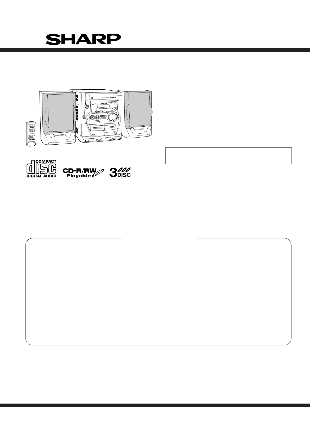
CD-XP120 Mini Component System consisting of CD-XP120
(main unit) and CP-XP120 (speaker system).
• In the interests of user-safety the set should be restored to its
original condition and only parts identical to those specified be
used.
CONTENTS
Page
IMPORTANT SERVICE NOTES........................................................................................................................................ 2
SPECIFICATIONS ............................................................................................................................................................. 2
NAMES OF PARTS ........................................................................................................................................................... 3
DISASSEMBLY.................................................................................................................................................................. 5
REMOVING AND REINSTALLING THE MAIN PARTS..................................................................................................... 7
ADJUSTMENT ................................................................................................................................................................... 9
TEST MODE .................................................................................................................................................................... 10
BLOCK DIAGRAM ........................................................................................................................................................... 12
SCHEMATIC DIAGRAM / WIRING SIDE OF P.W.BOARD............................................................................................. 16
VOLTAGE ........................................................................................................................................................................ 33
NOTES ON SCHEMATIC DIAGRAM .............................................................................................................................. 34
TYPES OF TRANSISTOR ............................................................................................................................................... 34
FUNCTION TABLE OF IC................................................................................................................................................ 35
FL DISPLAY..................................................................................................................................................................... 39
REPLACEMENT PARTS LIST/EXPLODED VIEW
PACKING OF THE SET
SHARP CORPORATION
This document has been published to be used
for after sales service only.
The contents are subject to change without notice.
Page 2
CD-XP120
IMPORT ANT SERVICE NOTES
BEFORE RETURNING THE AUDIO PRODUCT
(Fire & Shock Hazard)
Before returning the audio product to the user, perform the
following safety checks.
1. Inspect all lead dress to make certain that leads are not
pinched or that hardware is not lodged between the chassis
and other metal parts in the audio product.
2. Inspect all protective devices such as insulating materials,
cabinet, terminal board, adjustment and compartment covers
or shields, mechanical insulators etc.
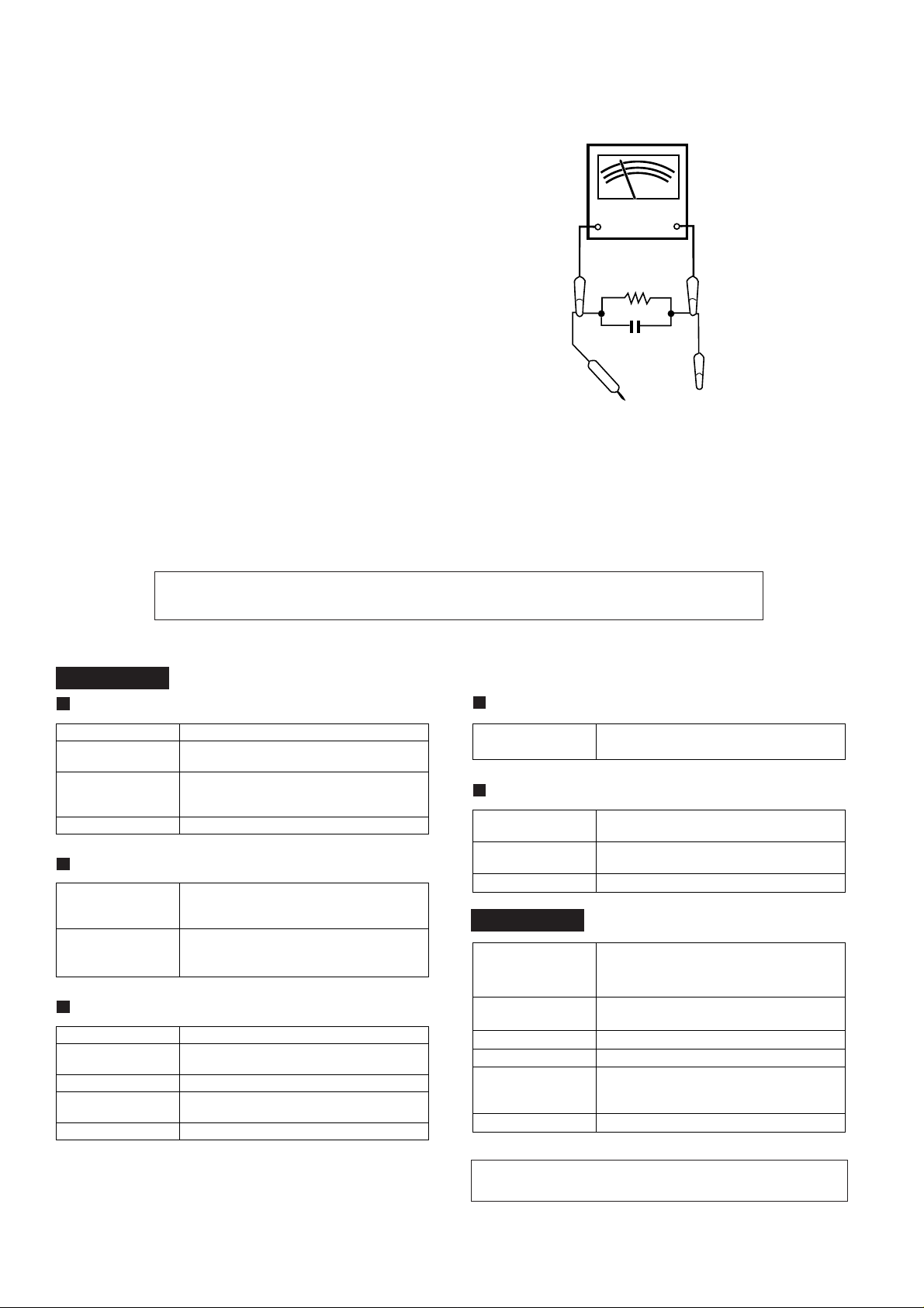
3. To be sure that no shock hazard exists, check for leakage
current in the following manner.
* Plug the AC line cord directly into a 120 volt AC outlet.
* Using two clip leads, connect a 1.5 kohm, 10 watt resistor
paralleled by a 0.15 µF capacitor in series with all exposed
metal cabinet parts and a known earth ground, such as
conduit or electrical ground connected to earth ground.
* Use a VTVM or VOM with 1000 ohm per volt, or higher,
sensitivity to measure the AC voltage drop across the
resistor (See diagram).
* Connect the resistor connection to all exposed metal parts
having a return path to the chassis (antenna, metal cabinet,
screw heads, knobs and control shafts, escutcheon, etc.)
and measure the AC voltage drop across the resistor.
VTVM
AC SCALE
1.5 kohms
10 W
0.15 µF
TO EXPOSED
TEST PROBE
METAL PARTS
CONNECT TO
KNOWN EARTH
GROUND
All check must be repeated with the AC line cord plug connection
reversed.
Any reading of 0.3 volt RMS (this corresponds to 0.2 milliamp.
AC.) or more is excessive and indicates a potential shock
hazard which must be corrected before returning the audio
product to the owner.
FOR A COMPLETE DESCRIPTION OF THE OPERATION OF THIS UNIT, PLEASE REFER
TO THE OPERATION MANUAL.
SPECIFICATIONS
CD-XP120
General
Power source AC 120 V, 60 Hz
Power consump-
tion
Dimensions Width: 10-5/8" (270 mm)
Weight 12.8 lbs. (5.8 kg)
Amplifier
Output power 20 watts minimum RMS per channel into 8
Output terminals Speakers: 8 ohms
CD player
Type 3-disc multi-play compact disc player
Signal readout Non-contact, 3-beam semiconductor laser
D/A converter 1-bit D/A converter
Frequency re-
sponse
Dynamic range 90 dB (1 kHz)
53 W
Height: 12" (305 mm)
Depth: 13-1/2" (343 mm)
ohms from 100 Hz to 20 kHz, 10% total harmonic distortion
Headphones: 16 - 50 ohms (recommended:
32 ohms)
pickup
20 - 20,000 Hz
Tuner
Frequency range FM: 87.5 - 108 MHz
AM: 530 - 1,720 kHz
Cassette deck
Frequency response
Signal/noise ratio 50 dB (TAPE 1, recording/playback)
Wow and flutter 0.3 % (WRMS)
CP-XP120
Type 2-way type speaker system
Maximum input
power
Rated input power 20 W
Impedance 8 ohms
Dimensions Width: 7-7/8" (200 mm)
Weight 4.6 lbs. (2.1 kg)/each
125 - 8,000 Hz (Normal tape)
50 dB (TAPE 2, playback)
Tweeter
4" (10 cm) Woofer
40 W
Height: 12" (305 mm)
Depth: 6-9/16" (167 mm)
Specifications for this model are subject to change without
prior notice.
– 2 –
Page 3
CD-XP120
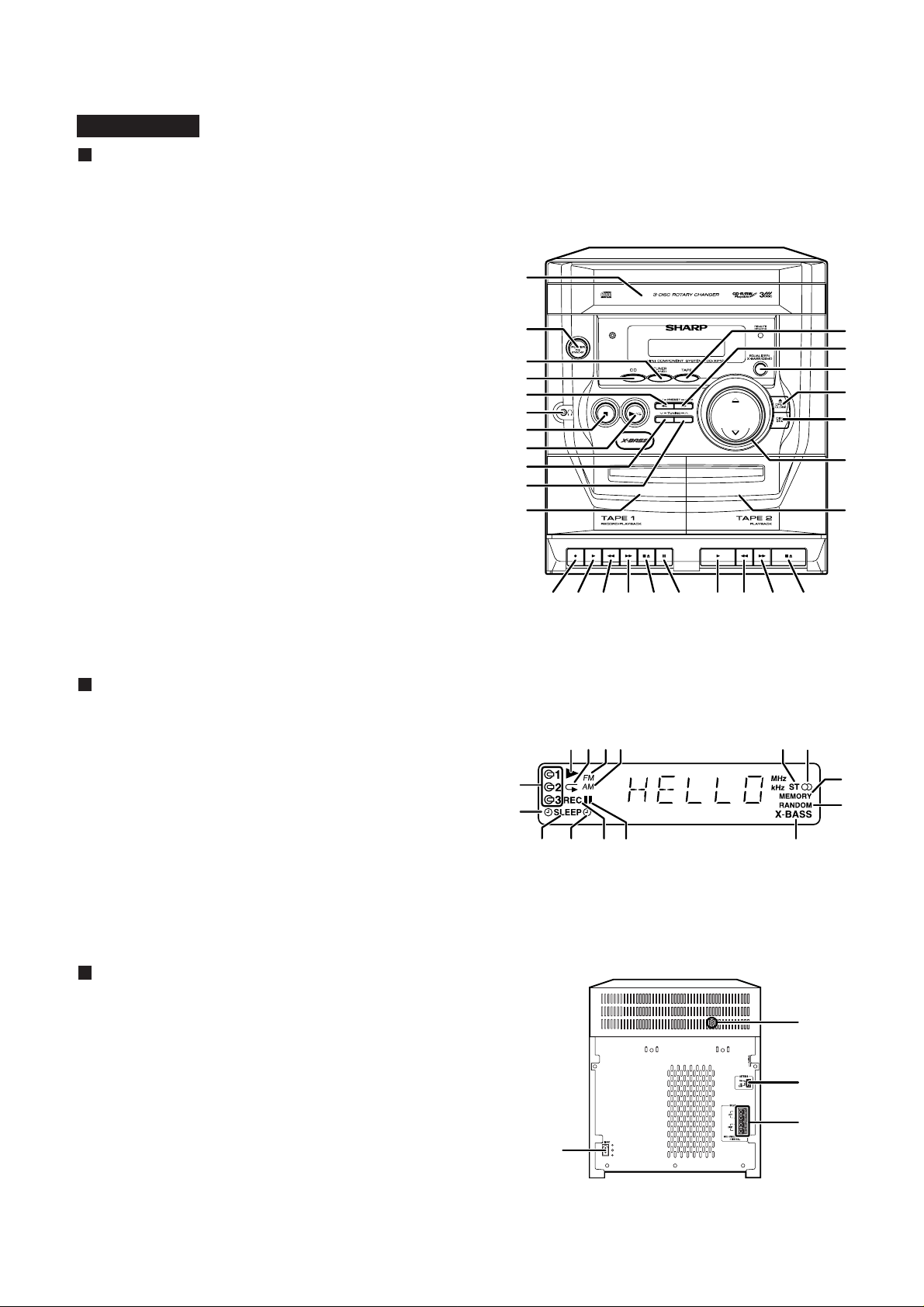
Front panel
1. Disc Tray
2. Power On/Stand-by Button
3. Tuner (Band) Button
4. CD Button
5. CD Track Down or Fast Reverse,
Tuner Preset Down Button
6. Headphone Jack
7. CD Stop Button
8. CD Play or Repeat Button
9. Tuning Down Button
10. Tuning Up Button
11. Tape 1 Cassette Compartment
12. Tape Button
13. CD Track Up or Fast Forward,
Tuner Preset Up Button
14. Equalizer Mode Select/Extra Bass/
Demo Mode Button
15. Disc Tray Open/Close Button
16. Disc Skip Button
17. Volume Up and Down Buttons
18. Tape 2 Cassette Compartment
19. Tape 1 Record Button
20. Tape 1 Play Button
21. Tape 1 Rewind Button
22. Tape 1 Fast Forward Button
23. Tape 1 Stop/Eject Button
24. Tape 1 Pause Button
25. Tape 2 Play Button
26. Tape 2 Rewind Button
27. Tape 2 Fast Forward Button
28. Tape 2 Stop/Eject Button
NAMES OF P ARTS
1
2
3
4
5
6
7
8
9
10
11
19
CD-XP120
12
13
14
15
16
17
18
20 21 22 23 24 25 26 27 28
Display
1. CD Play Indicator
2. CD Repeat Play Indicator
3. FM Station Indicator
4. AM Station Indicator
5. Disc Number Indicators
6. Clock Indicator
7. Sleep Indicator
8. Timer Play Indicator
9. Tape 1 Record Indicator
10. CD Pause Indicator
11. FM Stereo Mode Indicator
12. FM Stereo Receiving Indicator
13. Memory Indicator
14. Random Play Indicator
15. Extra Bass Indicator
Rear panel
1. AC Power Input Jack
2. Transport Screw
3. FM/AM Loop Antenna Jack
4. Speaker Terminals
1 2 3 4 11 12
5
6
8
7 9 10 15
13
14
2
3
4
– 3 –
1
Page 4
CD-XP120
CD-XP120
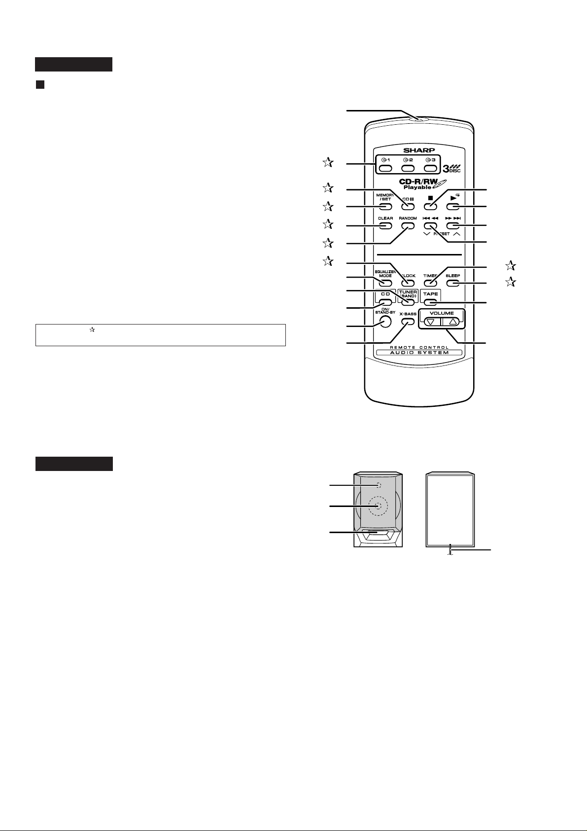
Remote control
1. Remote Control Transmitter
2. Disc Number Select Buttons
3. CD Pause Button
4. Memory/Set Button
5. Clear Button
6. CD Random Button
7. Clock Button
8. Equalizer Mode Select Button
9. Tuner (Band) Button
10. CD Button
11. Power On/Stand-by Button
12. Extra Bass Button
13. CD Stop Button
14. CD Play or Repeat Button
15. CD Track Up or Fast Forward,
Tuner Preset Up Button
16. CD Track Down or Fast Reverse,
Tuner Preset Down Button
17. Timer Button
18. Sleep Button
19. Tape Button
20. Volume Up and Down Buttons
Buttons with " " mark in the illustration can be operated on the remote control only.
10
11
12
1
2
3
4
5
6
7
8
13
14
15
16
17
18
9
19
20
CP-XP120
1. Tweeter
2. Woofer
3. Bass Reflex Duct
4. Speaker Wire
1
2
3
4
– 4 –
Page 5
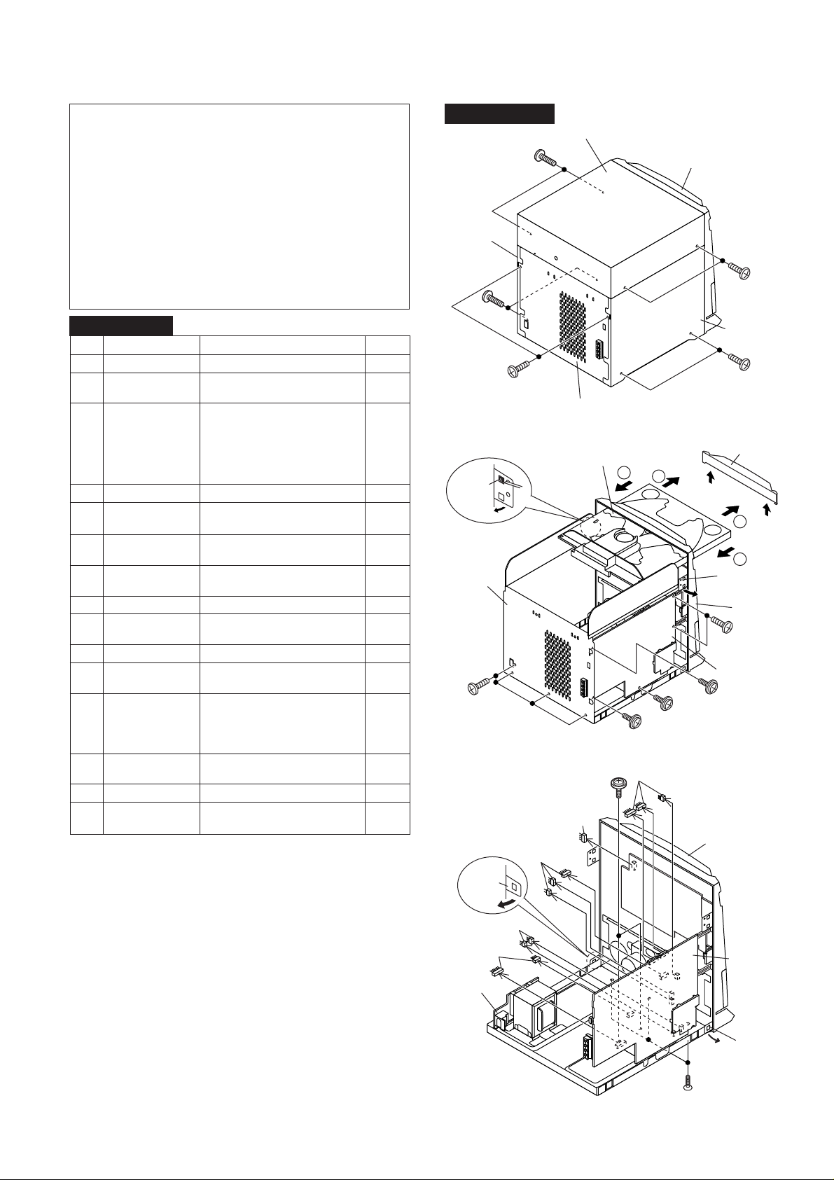
DISASSEMBLY
Caution on Disassembly
Follow the below-mentioned notes when disassembling
the unit and reassembling it, to keep it safe and ensure
excellent performance:
1. Take cassette tape and compact disc out of the unit.
2. Be sure to remove the power supply plug from the wall
outlet before starting to disassemble the unit.
3. Take off nylon bands or wire holders where they need to
be removed when disassembling the unit. After servicing
the unit, be sure to rearrange the leads where they were
before disassembling.
4. Take sufficient care on static electricity of integrated
circuits and other circuits when servicing.
CD-XP120
Side Panel
(Right)
(B1)x2
ø3x10mm
(A1)x2
ø3x16mm
CD-XP120
Top Cabinet
Front
Panel
(A1)x2
ø3x16mm
CD-XP120
STEP
10
11 Turntable 1. Screw .......................(L1) x1 6-2
12 Loading Tray 1.
13 CD Servo PWB 1. Screw ...................... (N1) x3 6-3
14 Switch B PWB 1. Screw ...................... (P1) x2 6-3
15 CD Mechanism 1. Screw ...................... (Q1) x4 6-4
Note 1:
1. After removing the connector for the optical pickup from the
REMOVAL PROCEDURE FIGURE
1 Top Cabinet 1. Screw ...................... (A1) x4 5-1
2 Side Panel 1. Screw ...................... (B1) x6 5-1
(Left/Right)
3 CD Player Unit 1. Turn on the power supply, .. 5-2
4 Rear Panel 1. Screw ...................... (D1) x6 5-2
5 Main PWB 1. Screw ...................... (E1) x5 5-2,5-3
6 Front Panel 1. Screw ....................... (F1) x3 5-3
7 Switch A PWB 1. Screw ...................... (G1) x3 6-1
8 Display PWB 1. Screw .................... (H1) x10 6-1
9 Tape Mechanism 1. Open the cassette holder. 6-1
Headphones PWB
(Note 1) 2. Socket ..................... (N2) x5
connector, wrap the conductive aluminium foil around the front end
of the connector so as to protect the optical pickup from electrostatic damage.
open the disc tray, take out
the CD tray cover, and close.
2. CD Tray Cover........ (C1) x1
3. Hook........................ (C2) x2
4. Socket ..................... (C3) x4 5-3
2. Socket ..................... (E2) x7 5-3
2. Hook.........................(F2) x2
2. Socket ..................... (G2) x1
2. Screw...................... (J1) x8
1. Screw ...................... (K1) x1 6-1
2. Spacer......................(L2) x1
Push forward the loading tray.
2.
Inserting the flat head into the
hole, push in the direction indi-
cated by the arrow. ...
2. Spring...................... (Q2) x4
(M1) x2
6-2
(C2)x1
Pull
Rear
Panel
(D1)x4
ø3x8mm
(F2)x1
(B1)x2
ø3x8mm
(E2)x3
Rear
Panel
Figure 5-1
CD Player
Unit
(D1)x1
ø3x10mm
Figure 5-2
(E1)x2
ø3x10mm
(C3)x1
2
(C3)x3
1
(E1)x1
ø3x10mm
Side Panel
(Left)
(B1)x2
ø3x10mm
(C2)x1
Pull
(E1)x2
ø3x8mm
Main PWB
(D1)x1
ø3x10mm
Front
Panel
(C1)x1
1
2
Front
Panel
– 5 –
Power
PWB
(E2)x2
(E2)x2
Figure 5-3
(F1)x3
ø3x6mm
Main PWB
(F2)x1
Page 6
CD-XP120
Display PWB
(H1)x10
ø2.5x10mm
Tape
Mechanism
(J1)x8
ø3x10mm
(G1)x3
ø2.5x10mm
(K1)x1
ø2.5x10mm
(L1)x1
ø3x8mm
Front Panel
Headphones
PWB
Figure 6-1
(L2)x1
Display PWB
Switch A
PWB
Open
Cassette
Holder
Screwdriver
(M1)x1
(G2)x1
CD Servo
PWB
(N2)x2
(Q1)x4
ø2.5x8mm
(Q2)x4
(N1)x3
ø3x24mm
(N2)x1
(N2)x1
Figure 6-3
CD Mechanism
(N2)x1
(P1)x2
ø3x8mm
Loading
Tray
Switch B
PWB
Loading Tray
Screwdriver
Turntable
Loading Tray
(M1)x1
Figure 6-2
CP-XP120
This speaker CP-XP120 is available in assembles only and
may not be disassembled.
Figure 6-4
– 6 –
Page 7
REMOVING AND REINSTALLING THE MAIN PARTS
TAPE MECHANISM SECTION
Perform steps 1 to 6 and 9 of the disassembly method to
remove the tape mechanism.
How to remove the record/playback and erase
heads (TAPE 1) (See Fig. 7-1)
1. When you remove the screws (A1) x 2 pcs., the record/
playback head can be removed.
2. Move the hooks (A2) x 2 pcs., toward the center position as
shown in Fig. 7-1 and then lift the erase head.
Hook
(A2)x2
(A1)x1
ø2x7mm
(A1)x1
ø2x3mm
CD-XP120
TAPE 1
Record/Playback
Head
How to remove the playback head (TAPE 2)
(See Fig. 7-2)
1. When you remove the screws (B1) x 2 pcs., the playback
head can be removed.
How to remove the pinch roller (TAPE 1)
(See Fig. 7-3)
1. When you remove the screw (C1) x 1 pc., the pinch roller
can be removed.
Note:
When installing the pinch roller, pay attention to the spring
mounting position.
How to remove the pinch roller (TAPE 2)
(See Fig. 7-3)
1. When you remove the screw (D1) x 1 pc., the pinch roller
can be removed.
Note:
When installing the pinch roller, pay attention to the spring
mounting position.
How to remove the motor (See Fig. 7-4)
1. Remove the belt.
2. Remove the screws (E1) x 6 pcs., to remove the motor
bracket.
3. Remove the screws (E2) x 3 pcs., to remove the motor.
Erase
Head
TAPE 1
(B1)x1
ø2x6mm
(C1)x1
ø2x4mm
Pinch Roller
Figure 7-1
(B1)x1
ø2x6mm
Figure 7-2
Playback
Head
TAPE 2
TAPE 2
(D1)x1
ø2x4mm
Pinch Roller
How to remove the belt (TAPE 1)
(See Fig. 7-5)
1. Remove the main belt (F1) x 1 pc., from the motor side.
2. Remove the FF/REW belt (F2) x 1 pc.
How to remove the belt (TAPE 2)
(See Fig. 7-5)
1. Remove the main belt (G1) x 1 pc., from the motor side.
2. Remove the FF/REW belt (G2) x 1 pc.
Motor
TAPE 2
Main
Belt
(G1)x1
REW/FF
Clutch Ass'y
REW/FF
Belt
(G2)x1
TAPE 2
Main Belt
(G1)x1
Main
Belt
(F1)x1
TAPE 1
Main Belt
(F1)x1
Motor
REW/FF
Belt
(F2)x1
TAPE 1
REW/FF
Clutch Ass'y
– 7 –
(E1)x2
ø2x4mm
Figure 7-3
(E1)x2
ø2x4mm
Motor
(E1)x2
ø2x4mm
Motor
Bracket
(E2)x3
Special Screw
Motor
Bracket
Motor
Figure 7-4Figure 7-5
Page 8
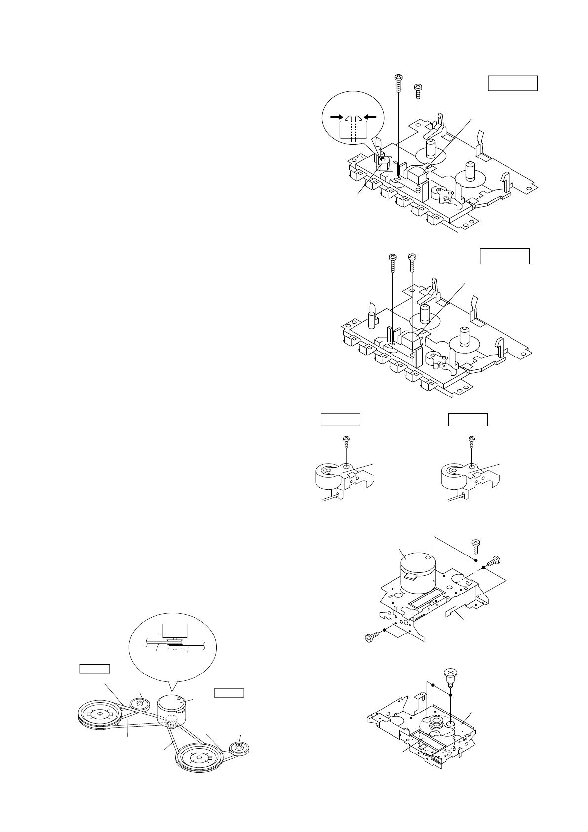
CD-XP120
CD MECHANISM SECTION
Perform steps 1, 2, 3, 11, 12, 13 and 15 of the disassembly
method to remove the CD mechanism.
How to remove the T/T up/down motor
(See Figs. 8-1, 8-2)
1. Remove the screws (A1) x 4 pcs.
2. Remove the belt (A2) x 1 pc.
3. Remove the screws (A3) x 2 pcs., to remove the T/T up/
down motor.
(A1)x4
ø3x8mm
(B1)x2
ø3x8mm
(B3)x2
ø2.4x3mm
(B1)x3
ø3x8mm
Loading
Tray
Figure 8-1
(A3)x2
ø2.4x3mm
How to remove the loading motor
(See Figs. 8-1, 8-2)
1. Remove the screws (B1) x 5 pcs.
2. Remove the belt (B2) x 1 pc.
3. Remove the screws (B3) x 2 pcs., to remove the loading
motor.
How to remove the pickup (See Fig. 8-3)
1. Remove the stop washer (C1) x 1 pc., to remove the gear
(C2) x 1 pc.
2. Remove the screws (C3) x 2 pcs., to remove the shaft
(C4) x 1 pc.
3. Remove the pickup.
Note
After removing the connector for the optical pickup from the
connector wrap the conductive aluminium foil around the front
end of connector so as to protect the optical pickup from
electrostatic damage.
(B2)x1
CD
Pickup
Mechanism
(C3)x1
ø2.6x6mm
(A2)x1
Figure 8-2
Stop Washer
(C1)x1
Loading
Motor
(C3)x1
ø2.6x6mm
Gear
(C2)x1
T/T Up/Down
Motor
Shaft
(C4)x1
– 8 –
Figure 8-3
Page 9
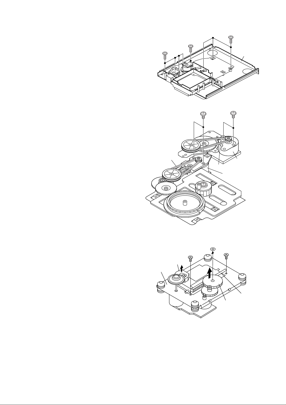
ADJUSTMENT
MECHANISM SECTION
• Driving Force Check
Torque Meter Specified Value
Play: TW-2111 Tape 1: Over 80 g
Tape 2: Over 80 g
• Torque Check
Torque Meter
Play: TW-2111 30 to 80 g.cm 30 to 80 g.cm
Fast forward: TW-2231 — 70 to 180 g.cm
Rewind: TW-2231 — 70 to 180 g.cm
• Tape Speed
Test Tape
Tape MTT-111 Variable 3,000 ± 30 Hz Speaker
speed Resistor in Terminal
Adjusting
Point
motor. (Load
TAPE MECHANISM
Variable Resistor in motor
Figure 9-1
VR351
T351
AM IF
FM MUTE
Level
TP302
R356
R357
AM BAND
COVERAGE fL
Tape 1
T306
L303
FM BAND
COVERAGE fL
T304
FM IF
Specified Value
Specified
Value
Tape
Motor
MAIN PWB
1
11 12
IC301
1
L302
FM RF
T302
AM TRACKING
fL
Tape 2
Instrument
Connection
resistance:
6 ohms)
22
R381
20
TP301
IC302
CNP301
CD-XP120
TUNER SECTION
fL: Low-range frequency
fH: High-range frequency
• AM IF/RF
Signal generator: 400 Hz, 30%, AM modulated
Test Stage Frequency Frequency
Display
AM IF 450 kHz 1,720 kHz T351 *1
AM Band — 530 kHz (fL): T306 *2
Coverage 1.1 ± 0.1 V
AM Tracking 990 kHz 990 kHz (fL): T302 *1
*1. Input: Antenna Output: TP302
*2. Input: Antenna Output: TP301
• FM RF
Signal generator: 1 kHz, 40 kHz dev., FM modulated
Test Stage Instrument
FM Band — 87.50 MHz L303 (fL): *1
Coverage 1.3 V ± 0.1 V
FM RF 98.00 MHz 98.00 MHz L302 *2
Frequency Frequency
Display
(10-30 dB)
*1. Input: Antenna Output: TP301
*2. Input: Antenna Output: Speaker Terminal
• FM IF
Signal generator: 10.7 MHz, FM modulated
Test Stage Instrument
IF 10.7 MHz 98 MHz T304 *1
Frequency Frequency
Display
*1. Input: Antenna Output: TP301
• FM Mute Level (FM ST MODE)
Signal generator: 1 kHz, 40 kHz dev., FM modulated
Frequency
Display
98.00 MHz 98.00 MHz VR351*1 Input:CNP301
(26 dBµV) Output: Speaker
Adjusting
*1. Adjust so that an output signal appears.
Setting/
Adjusting
Parts
Setting/
Adjusting
Point
Setting/
Adjusting
Point
(Turn the
core of transformer T304
fully counterclock wise)
Parts
Instrument
Connection
Connection
Connection
Instrument
Connection
Terminal
Figure 9-2 ADJUSTMENT POINTS
– 9 –
Page 10
CD-XP120
TEST MODE
PLAY + DISC SKIP test04 TIMER ON/OFF TEST MODE
FL DISPLAY:
STOP + DISC SKIP test05 VFD DISPLAY WINDOW TEST MODE
FL DISPLAY: VFD ALL LIGHT
FUNCTION: TEST THE VFD DISPLAY WINDOW
PLAY + OPEN/CLOSE test08 OPEN/CLOSE & 3 DISC CHANGER AGING TEST
DISPLAY:
FUNCTION: Enter the TEST MODE 8, MCU control the 3 DISC CHANGER OPEN/CLOSE.
After open finished, tray rotate 1 circle (360 degree). Then close, After close
finished, tray rotate 1 circle (360 degree) again.
Request: Every period include 4 operation. Below is TIMING:
Enter test mode
CHANGER
Find the disc 1 position
open
delay 3S after open finish
rotate 1 circle
close
delay 3S after close finish
rotate 1 circle
– 10 –
Page 11
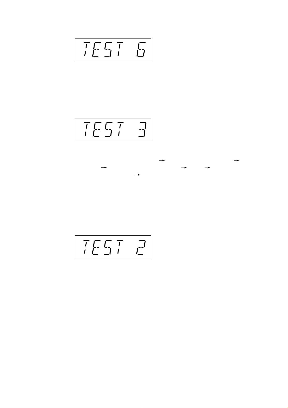
PLAY + VOLUME DOWN test06 FRONT PANEL KEY TEST
FL DISPLAY:
CD-XP120
FUNCTION:
F RONT PANEL KEY TEST MODE,IF ALL KEY HAVE BEEN PRESSED 1 TIME,
THEN
PRESS THE "POWER" KEY, VFD DISPLAY "OK".
PLAY + VOLUME UP test03 VOLUME TEST MODE
FL DISPLAY:
FUNCTION:
1. TEST 3 DISPLAY 1 SECOND. THEN CHANGE TO CD FUNCTION.
2. IN CD FUNCTION (Pickup IN CHECK DISC1 SW TOC_IL No
DISC RECEIVE OPEN/CLOSE KEY OPEN RECEIVE
OPEN/CLOSE KEY CLOSE)
3. Can change to other function [TAPE/TUNER] FUNCTION KEY PROCESS
SAME AS NORMAL PROCESS.
4. In any function within this test mode VOLUME CONTROL HAS
3LEVEL [0/23/MAX] CANCEL VOL UP/DOWN CONTINUE PROCESS
FUNCTION.
PLAY + TUNER test02 TUNER TEST MODE
FL DISPLAY
FUNCTION STORE 10 PRESET TUNER IN THE MEMORY [AM/FM ST]
FM test use the BAND key change from FM ST.
– 11 –
Page 12
CD-XP120
ACTUATOR
FO+
TR+
TR–
FO–
SW1
OPEN/
CLOSE
SW2
DISC
SW3
UP
T/T UP/DOWN
LOADING MOTOR
CD LOADING
SPINDLE
PICKUP IN
M
M3
M
M1
MOTOR
NM802
MOTOR
NM801
SLED
MOTOR
SW4
M_GND
LOAD SW
DISC_SW
UP_SW
LOAD+
LOAD–
ROTATE
Q405
Q403
GND
PO1+
Q404
15 16 17 18 19
OPO
PO1–
Q406
Q407
D403
Q408
Q409
Q410
O/C SW
LOAD_SW
DISC_SW
PICK_IN
+
–
M+
M–
ROTATE+
ROTATE-
+
–
+
M
M
SP+
SP–
–
SL+
+
SL–
PU-IN
–
GND
TR–
TR+
FO+
FO–
GND
PD
VR
LD
1 2 3 4
VG1
VIN1
VO1–
VO1+
VIN4
VO4+
VO4–
GND
FOCUS/TRACKING/SPIN/SLED DRIVER
6
5
7
TRB
REG O
IC404
BIAS
VG4
Q402
D402
8
9
10 11 12 13 14
VG2
GND
VIN2
MUTE
VIN3
VG3
VCC
VCC
20 21 22 23 24 25 26 27 28
IC404
MM1469XH
VO2+
VO3+
VO2–
VO3–
+
–
C
+
–
F
+
–
B
+
–
A
+
–
E
GND
MON
LD
VCC
PICKUP UNIT
1/2V
C
F
B
A
E
+5V
LASER
DRIVER
Q401
32 31 30 29 28 27 26 25 24 23 22 21 20
A
AN22000A
HEAD AMP.
LD
PD
123456789
DBC
IC402
RFN
VCC
E
RFOUT
F
RFIN
TBAL
CACC
FBAL
GCTL
CEA
ARF
10 11 12 13 14 15 16
FEOUT
3TOUT
FEN
CBDO
TEN
BDO
19 18 17
TEBPF
TEOUT
OFTR
CDFTR
VDET
NRFDET
VREF
GND
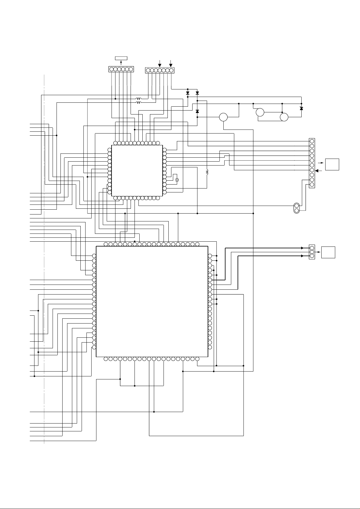
Figure 12 BLOCK DIAGRAM (1/4)
– 12 –
Page 13
CD-XP120
CNS701
MDATA
MLD
37
38
39
40
41
42
43
44
45
46
47
48
CNP701
34612
5
STB
CLK
POW_SW
D_GND
DATA
INTR
36 35 34 33 32 31 30
SD
STB
CLK
DATA
UP_SW
DISC_SW
LOAD_SW
PICK_IN
CD_STB
NRST
MMOD
MCLK
BLKCK
P0W_KEY
IC403
IX0051SJ
SYSTEM
MICROCOMPUTER
GVSW
ROTATE
LOAD-
LOAD+
STAT
MRST
1 2 3 4 5 6 7 8 9
7564312
D_GND
29 28 27 26 25
IR
CD+B
SYS_STOP
TAPE_DET
DEMO
10 11 12
+B2
6.2V
M_GND
CHANEL_SW
P_STB
FM_ST
CE
P_MUTE
CL
DO
DI
XO
XI
VSS
OSC1
OSC2
MODE_CHK
P_CON
P_STB
24
23
22
21
20
19
18
17
16
15
14
13
+B6
5.6V
P_MUTE
VDD
CNS101
X402
8 MHz
D401
D404
D405
Q411
CONSTANT
VOLTAGE
Q412
Q413
FM_ST
CD+B
TAPE_DET
ZD401
CNS105
SD
DO
CL
DI
CE
1
2
3
4
5
TO MAIN
SECTION
6
CNP105
7
+B5
8
9
10
1
2
19 18 17 16 15 14 13 12 11 10
20
/RST
PMCK
TVR
21
22
TVD
23
PC
24
ECM
25
ECS
26
KICK
27
TRO
28
FOO
29
VREF
30
FBAL
31
TBAL
FE
32
TE
33
RFENV
34
35
VDET
36
OFT
37
TRCRS
38
/RFDET
39
BDO
40
LD
WVEL
TDFS
PLLF1
41 42 43 44 45 46 47 48 49
STAT
SUBQ
SQCK
BLKCK
ARF
DMUTE
IREF
/TLOCK
MN6627482W
CD SIGNAL CONTROL
VCOF
PLLF
DSLF
DRF
9 8 7 6 5 4 3 2 1
/FLOCK
SENSE
MLD
MCLK
MDATA
DVSS1
DVDD1
SRDATA
LRCK
TX
IC401
X2
X1
VSS
SBCK
SUBC
VCDF2
PCK
EFM/CK384
AVSS2
AVDD2
50 51 52 53 54 55 56 57 58 59 60
BCLK
SSEL
MSEL
PSEL
CSEL
RSEL
OUTR
AVSS1
OUTL
AVDD1
/TEST
IOSEL
RESY
DEMPH
CLVS
FLAG
IPFLAG
FCLK
CLOCK
BYTCK
VDD
CRC
CD_R
A_GND
80
79
78
77
CD_L
CNS103
3
TO MAIN
2
SECTION
CNP103
1
76
75
74
73
72
71
70
69
68
67
66
65
64
63
62
61
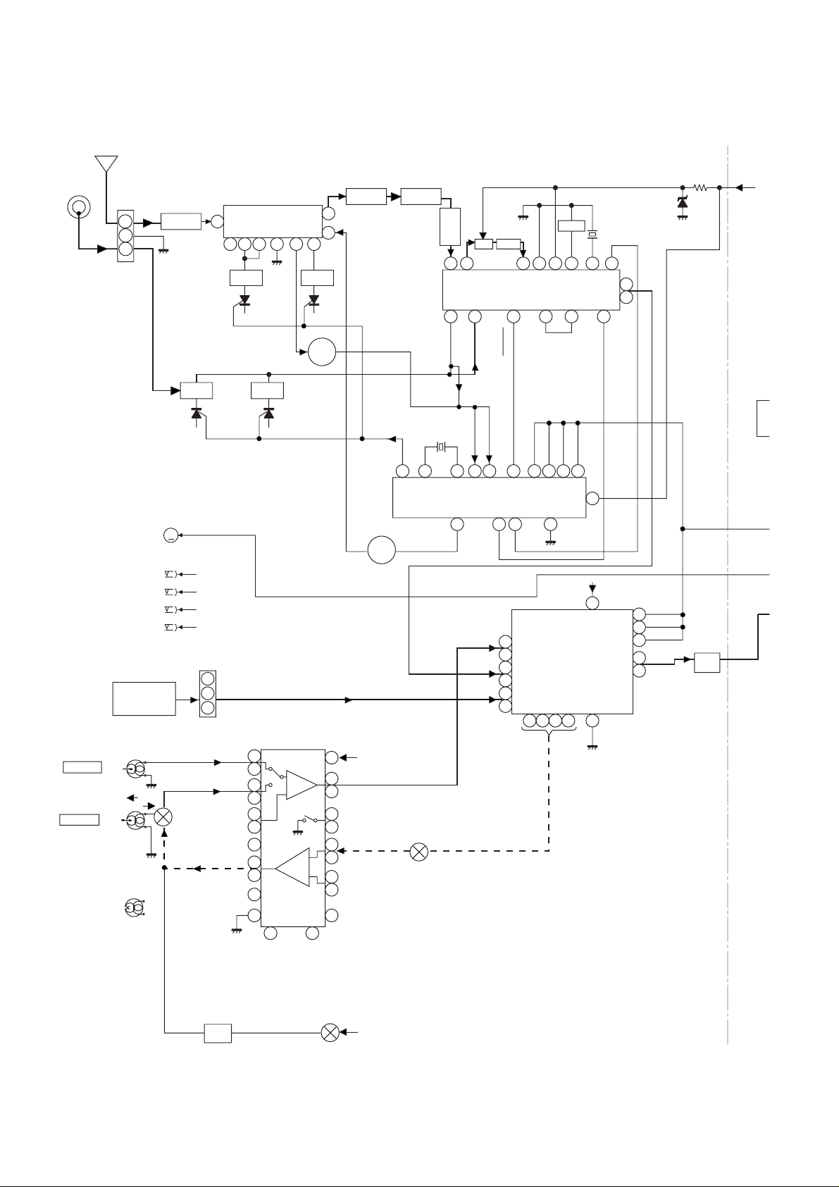
Figure 13 BLOCK DIAGRAM (2/4)
– 13 –
Page 14
CD-XP120
R
E
C
AM LOOP
ANTENNA
TAPE 2
PLAYBACK
HEAD
TAPE 1
RECORD/
PLAYBACK HEAD
ANTENNA
CNP301
T2 FF/REW
CD SECTION
L-CH
R-CH
L-CH
R-CH
AC BIAS
ERASE
HEAD
FM
3
2
1
SW5
T1 PLAY
SW6
T1 FF/REW
SW7
SW8
T2 PLAY
FROM
CNS103
REC
P.B.
B.P.F
BF301
M2
TAPE
MOTOR
M
SWITCHING
SW801
B, C, D,
F, G
IC301
TA7358AP
1
FM FRONT END
4
3
L302
5
T306
2
FM RF
AM TRACKING
T302
SP DET
+B3
+B3
+B3
+B3
CNP103
1
2
3
AN7345K
PLAYBACK AND RECORD
/PLAYBACK AMP.
L(T1)
1
R(T1)
24
2
L(T2)
R(T2)
23
L NF
3
R NF
22
6
L REC
R REC
REF
16
14
12
REC
9
15
7
FM
OSC BUFF
AM BAND
COVERAGE
IC801
P.B
T1/T2
8
OSC
L303
Q302
19
6
13
18
17
10
9
21
20
4
5
7
8
FM
L
R
L REC
R
L NF
R NF
ALC
FM IF
+B4
T302
FM OSC
VT
Q360
SWITCHING
PB
20
FM
CF303
4.5 MHz
1
SW801
A, E
CF302
1
AM MIX
23
AM OSC IN
X352
22
OSC
PLL(TUNER)
7
T351
AM IF
2
IC303
LA1832S
21
AM RF IN
1615
IC302
LC72131
FM/AM
TAPE
TUNER
CD
CF351
CF352
4
985
GND
VCC
FM/AM
MPXIN
OUT
18
7
IC303
LA1832S
STEREO
FM IF DET./
FM MPX./AM IF
CL
DI
CE
4
5
3
21
IC601
LC75341M
AUDIO PROCESSOR
8
7
17
18
L
R
L
R
L
R
AM IF
9
10
15
11
14
12
13
11
MO/ST
10
FM
DET
16
6
+B4
DO
17
VCO
17
23
456 kHz
MO/ST
FM/AM
12
3
X351
13
L
R
14
15
DI
CE
CL
DZ5.1BSJ
1
2
24
21
R
L
4
Q203
Q204
SYSTEM
MUTE
+B4
F
S
BIAS
OSC
Q801
L801
SW801
H
+B4
Figure 14 BLOCK DIAGRAM (3/4)
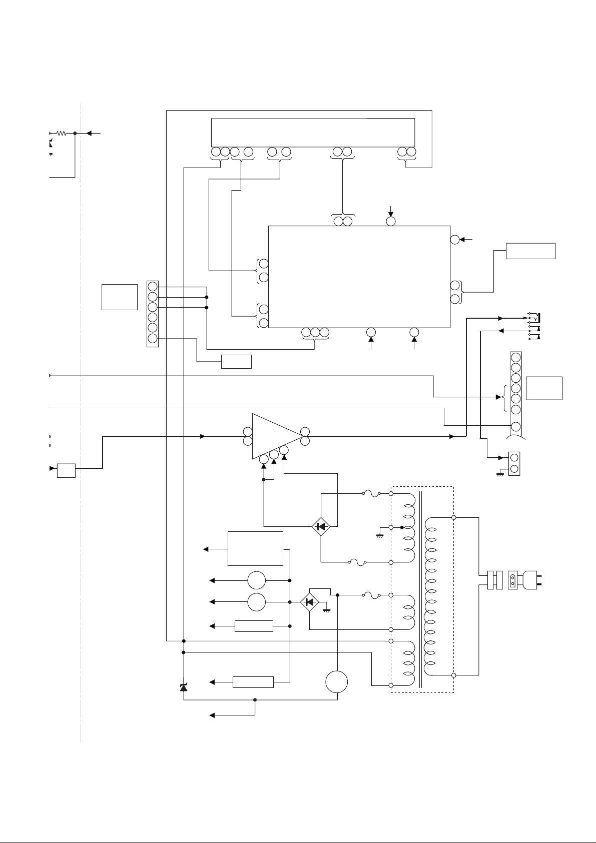
– 14 –
Page 15
CD-XP120
Q203
Q204
SYSTEM
MUTE
+B4
FROM CD
SECTION
CNS702
CNP702
1
2
3
4
5
6
2
1
~
3
SW701
L
R
IC201
LM1876TF
POWER AMP.
13
10
FL701
FL DISPLAY
31
~
18
29
15
~
26
30
~
37
8
VccB
15
+B1
VccA
2
4
Vee
11
7
–B1
30
5251
IC701
SC16312
SYSTEM
MICROCOMPUTER
DIN
STB
CLK
68
9
R-OUT
L-OUT
3.15A/125V
14
+B2
F101
VDD
+B4
46
VDD
3332
VEE
VDD
KEY3
KEY1
~
38
13
10
+B2
KEY
SW702~SW715
~
JK101
HEADPHONES
27
-B2
CNP105
1
2
3
FROM CD
SECTION
4
CNS105
5
6
SP DET
9
SO102
SPEAKER
TERMINAL
VF2
VF1
+B2
+B3
+B4
+B5
+B6
-B2
5.6 V
M10 V
REGULATOR
A12 V
6.2 V
D108~D111
IC101
MC7805CT
VOLTAGE
REGULATOR
Q103
VOLTAGE
Q104
VOLTAGE REGULATOR
Q109,Q110
VOLTAGE REGULATOR
Q105,Q106
VOLTAGE REGULATOR
-30 V
D112~D115
Q101
REGULATOR
Figure 15 BLOCK DIAGRAM (4/4)
– 15 –
F102
3.15A/125V
F103
1.6A/125V
VOLTAGE
T101
POWER TRANSFORMER
AC POWER
SUPPLY CORD
AC 120 V,60 Hz
Page 16
CD-XP120
P23 12 - C
FROM
A
CNP105
FM SIGNAL
PLAYBACK SIGNAL
CD SERVO PWB
CNS105 CNS101 CNS103
1 2 3 4 5 6 7 8 9
DI
CL
SD
DO
FM ST
10
CE
CD+B
TAPE_DET
P23 9 - A
FROM
CD SERVO PWB
7 6 5 4 3 2 1
STB
M_GND
CD_6.2V
CHANEL_SW
MUTE
D_GND
P23 12 - D
FROM
CD SERVO PWB
CNP101
5V
3 2 1
CD_R
A_GND
CNP103
CD_L
RECORD SIGNAL
B
C
D
SO101
E
F
G
CD SIGNAL
AC POWER
SUPPLY CORD
T101
POWER
AC INLET
TRANSFORMER
AC 120 V, 60 Hz
R121
4.7M
POWER PWB-A3
1
212
3
4
5
6
7
8
BI104
CNS104
SD
1
FM ST
2
DO
3
CL
4
CE
5
DI
6
A_12V
7
D_GND
P21 12 - D, E
8
TUN_L
TO TUNER SECTION
9
TUN_R
10
A_GND
11
CNP104
1
2
3
3
4
4
5
5
6
6
7
7
C141
100/16
3.15A/125V
3.15A/125V
VF1
VF2
F101
F102
F103
1.6A/125V
C142
0.022
100/50
1N4004
C101
D101
R129
+B
+B
A_GND
D108
D111
C105
0.1
C106
0.1
C107
220/50
D103
ZD101
DZ30BSB
A 12V
D109
1N5402M
D110
1N5402M
D112
1N4004
D115
1N4004
R101
22K
KSA1015 GR
VLTAGE
REGULATOR
Q101
C108
47/50
R103
47K
R102
10
D113
1N4004
D114
1N4004
+B
+B1
–B1
DZ6.2BSA
ZD102
+B
-B
-B
+B
C110
C109
330/35
CNP102
FROM DISPLAY PWB
10
1N5402M
C103
0.1
C104
0.1
1N5402M
D102
1N4004
C102
100/50
1N4004
+B
+B2
R104
12K
100/35
R105
330
R106
330
+B
–30V
5.6V
3.8V
3.8V
1 2 3 4 5
CNS102
P25 12 - G
+B
+B
D_GND
R133
1.2K
KRA102 M
+B
+B1
A_GND1
–B1
+B
Q103, Q104: VOLTAGE REGULATOR
20V
+B
R109
+B
20V
R107
1.2K
R108
100
C111
100/25
1
23123
Q112
+B
C112
4700/35
Q110
Q109
KRC107 M
KRA102 M
3
3
2
+B
1
Q105, Q106, Q109, Q110: VOLTAGE REGULATOR
Q103
2SD2012 Y
47
20V
13V
DZ13BSA
11.7V
Q104
2SD2012 Y
47
R110
12.3V
Q102
HSC1609 GR
R111
4.7K
ZD103
Q111
KRC107 M
R113
22K
11.7V
R114
22K
C113
100/25
+B
D104
C118
2200/35
R124
1
C114
470/25
1N4148
820
Q105
2
C115
0.022
+B
C116
C117
2200/35
Q106
2SD2012 Y
R116
47
HSC1609 GR
R117
4.7K
100
R115
ZD104
DZ8.2BSC
+B
D105
1N4004
C119
10/16
C143
220/25
0.022
D107
1N4004
CD_6.2V
22K
R118
D106
C121
0.022
1N4148
C120
100/25
D116
1N4004
D117
1N4004
M_GND
IC101
MC7805CT
VOLTAGE
REGULATOR
+B
2
D119
C123
1N4004
0.047
+B
C122
470/16
+B
+B
3 1
C124
47/25
H
• NOTES ON SCHEMATIC DIAGRAM can be found on page 34.
1
23456
Figure 16 SCHEMATIC DIAGRAM (1/10)
– 16 –
Page 17

2200/35
1
NP103
D107
1N4004
Q106
2SD2012 Y
CD_6.2V
22K
16
R118
7
D106
C121
1N4148
R117
4.7K
ZD104
C120
8.2BSC
100/25
OLTAGE REGULATOR
R
+B
D116
D105
1N4004
1N4004
C119
10/16
MC7805CT
VOLTAGE
REGULATOR
+B
C143
220/25
D119
1N4004
D117
1N4004
M_GND
IC101
2
0.022
C123
0.047
CD-XP120
P19 12 - A, B
TO TAPE SECTION
7 2 1 4 3 5 6 8 910
R618
+10V
M_10V
REC L
REC R
A_GND
M_GND
TAPE L
D603
1N4004
TAPE R
CHANEL_SW
+B
1K
1K
R201
R202
+B
+B
C208
470/16
R221
47K
+B
R208
R207
10K
10K
Q201
KSC1815 GR
ZD201
DZ3.3BSB
R216
10K
TAPE_DET
+B
D602
1N4004
D601
1N4004
+B
-B
+B
C122
470/16
-B
+B
+B
+B
3 1
C124
47/25
+B
33K
R620
R616
560
33K
TAPE L
TUN L
33K
100K
R214
R619
+IN B
ZD204
33K
–IN B
R203
C201
R220
4.7K
DZ3.3BSB
CD L
CD R
TUN R
TAPE R
R621
560
LM1876TF
POWER AMP.
MUTE B
1K
47/50
KSC1815 GR
KSC1815 GR
R624
7.5K
R625
7.5K
R617
R
L
VCC B
STB B
15 14 13 12 11 10
10K
R211
C604 10/16
C605 10/16
C606 10/16
R604
1K
IC601
LC75341M
AUDIO
PROCESSOR
C601 10/16
C602 10/16
C603 10/16
R605
1K
R601 1K
R602 1K
R603 1K
IC201
–IN A
+IN A
GND B
+B
–B
Q204
Q203
C207
47/25
MUTE A
STB A
9 8 7 6 5 4 1 2 3
Q202
HSC1609 GR
R215
4.7K
GND A
C203
47/50
R205
100K
R204
R206
1K
C202
47/50
R213
100K
SYSTEM
L
MUTE
R219
R218
R
SYSTEM
MUTE
R210
10K
10K
R209
R217
10K
R614
10K
1K
1K
R608
R606
C607
12 11 10
9 8 7 6 5 4 3 2 1
L1L2L3
L4
R4R3R2
R1
13 14 15 16 17 18 19
C608
4.7/50
R615
1K
1K
R607
10K
R609
R611
47K
OUT B
OUT A
VCC A
VEE
C204
47/50
-B
100K
+B
-B
10K
10K
C205
100/16
ZD203
DZ3.3BSB
4.7/50
47K
R610
LSL0
RSL0
C610
C609
C612
LIN
RIN
0.0027
C611
2.2/50
2.2/50
C613
LTRE
RTRE
R613
0.0027
C614
3.9K
3.9K
R612
C615
0.47/16
0.1
C622
0.1(ML)
CE
VSS
LOUT
LBS
VDD
VREF
ROUT
RBS
20 21 22 23 24
C617
33/16
0.1
C623
0.1(ML)
C616
CL
0.47/16
DI
R622
100K
C618
CE
R119
4.7
C127
C125
C126
R120
DI
CL
C128
0.1
4.7
+B
0.1
0.1
0.1
100/16
+B
R123
L101
3 µH
R122
10
L102
3 µH
10
C134
R623
100K
C619
220P
C620
220P
C621
220P
0.0047
C133
0.0047
CNP108
L IN
L OUT
A_GND
R OUT
R IN
+
L-ch
SO102
–
SPEAKER
TERMINAL
–
R-ch
+
BI108CNS108
L IN
5
5
5
4
3
2
1
L OUT
4
4
A_GND
3
3
R OUT
2
2
R IN
1
1
HEADPHONES PWB-A4
L103
10 µH
R128
390
R127
390
HEADPHONES
JK101
MAIN PWB-A1(1/3)
7
8 9 10 11 12
Figure 17 SCHEMATIC DIAGRAM (2/10)
– 17 –
Page 18

CD-XP120
8
9
R820
68K
39K
A
B
C
TAPE 2
PLAYBACK HEAD
R-CH
L-CH
D
MAIN PWB-A1(2/3)
SW5
TAPE 1
PLAY
SW6
TAPE 1
FF/REW
SW7
TAPE 2
FF/REW
SW8
TAPE 2
PLAY
M
+
–
CNS804
M2
TAPE
MOTOR
PLAYBACK SINGAL
RECORD SINGAL
1
1
2
2
3
3
CNP801
T1_R
A_GND
T1_L
C801
560P
C802
560P
CNP803CNS803
4
4
3
3
2
2
1
1
D802
1N4148
2
3
2
1
1
CNP804
R801
1K
R802
1K
R806
56
C808
330P
D804
1N4148
R808
10K
C810
100/25
C812
0.0027
C815
0.033
R809
100K
R834
33K
+B
R835
18K
D803
1N4148
33K
R813
D806
1N4148
C819
5.6K
R815
0.0022
R817
R818
E
F
TAPE 1
PLAYBACK/RECORD
HEAD
L-CH
R-CH
ERASE HERD
G
560P
C813
R811
C817
C805
330P
SW801C
REC./P.B.
R
CNP802
1
1
2
2
3
3
4
4
P
SW801D
REC./P.B.
R
SW801B
REC./P.B.
P
R
P
SW801F
REC./P.B.
P
SW801G
REC./P.B.
R P
T2_R2
T2_R1
A_GND
T2_L1
T2_L2
R
C803
560P
C804
560P
RECORD/PLAYBACK AMP.
R804
1K
IC801
PLAYBACK AND
24 23 22 21 20 19 18 17 16
R(T2)
L(T2)
C809
56
R805
10K
R NF
L NF
330P
560P
C814
R810
100K
C816
0.033
PRO
PLO
R814
33K
R803
1K
R(T1)
L(T1)
1 2 3 4 5 6 7 8 9
330P
C806
C811
100/25
R807
C807
0.0027
3.9K
L:T1
H:T2
IC801
AN7345K
3.9K
R812
C818
5.6K
R816
47/25
RRI
RLI
47/25
C821
3.3/50
C820
0.0022
R NF
L NF
RRO
RLO
C822
1
R
H
• NOTES ON SCHEMATIC DIAGRAM can be found on page 34.
1
23456
Figure 18 SCHEMATIC DIAGRAM (3/10)
– 18 –
Page 19

CD-XP120
R
NF
330P
B-A1(2/3)
R834
R835
18K
D803
1N4148
04
148
C812
0.0027
08
0K
R813
C815
0.033
R809
100K
33K
+B
33K
D806
1N4148
C819
5.6K
R815
0.0022
R817
R818
R838
5.6K
3.9K
6.8K
R821
C823
0.001
1.5K
R837
1K
R824
100
R823
C827
0.022
47K
C829
0.0033
10K
R826
C831
R828
47K
47/25
+B
C840
220/16
CHANEL_SW
TAPE L
TAPE R
REC R
REC L
+10V
M_GND
A_GND
TAPE_DET
M_10V
10
1
2
3
4
5
6
7
8
9
P17 8 - A
TO MAIN SECTION
C825
3.3/50
0.0022
R NF
L NF
22/50
RRO
RLO
ALC
10 11 12
C822
0.022
6.8K
R819
3.9K
R820
REF
C826
22/50
C824
0.001
560P
C813
R811
C817
47/25
3.9K
L:T1
IC801
AN7345K
3.9K
R812
C818
5.6K
R816
33K
H:T2
RRI
RLI
47/25
C821
C820
2 21 20 19 18 17 16 15 14 13
PRO
L NF
PLO
3 4 5 6 7 8 9
560P
C814
R810
100K
C816
0.033
R814
5
K
+B
VCC
R822
R
P
1.5K
SW801E
REC./P.B.
SW801A
REC./P.B.
C828
0.022
100
R825
P
R
C830
0.0033
C833
22/50
C832
10K
R827
C834
220/16
47/25
C835
0.022
SW801H
REC./P.B.
R830
100
C838
0.022 (ML)
+B
D801
1N4004
P R
+B
R831
150
R832
33K
C839
0.0047
(ML)
BIAS OSC.
Q801
KSC3203 Y
R833
10
+B
R836
8.2K
C836
0.0022
R829
220
+B
D805
1N4148
L801
BIAS OSC.
C837
100/10
7
8 9 10 11 12
Figure 19 SCHEMATIC DIAGRAM (4/10)
– 19 –
Page 20

CD-XP120
2
T
L
+
C
A
B
C
D
E
AM LOOP
ANTENNA
FM
ANTENNA
FM SIGNAL
AM SIGNAL
C302
0.001
D301
1N4148
D302
1N4148
BF301
B.P.F
1 2 3
1 2 3 4 5 6 7 8 9
C319
18P(CH)
D306
1N4148
D305
D307
1N4148
1N4148
0.01
AM
1
1
GND
2
2
FM
3
3
CNP301
C301
0.012
C304
C305
0.0047
0.8V
C307
C306
0.0047
1.5V
9P(UJ)
FM RF
C308
0.022
L302
5.2V
C303
0.001
C309
R302
R301
0.001
100K
22
1.5V
C318
5P
R303
VD303
33K
AM TRACKING fL
AM ANTENNA
0.022
C337
0.022
IC301
TA7358AP
FM FRONT END
0V
5.2V
T304
KDV147B
FM IF
C311
10P(CH)
R304
47K
Q302
SSC1674 C
OSC BUFF
T302
C329
AM OSC.
T306
AM BAND
COVERAGE fL
R307
FM BAND
COVERAGE fL
R315
47
33
C335
560P
R323
68K
4.4V
R306
C312
33P
L303
FM OSC.
R305
680
100P
C315
33
C330
12P(CH)
3.8V
2
6P
C313
C314
22P(CH)
C316
C331
0.047
C334
27P(UJ)
CF303
13
(UJ)
R308
10K
10/16
VD302
+B
C317
C332
0.022
5.2V
+B
KDV147B
0.022
VD301
R316
330
R312
2.2K
Q306
SSC1674 C
680
R313
SVC348S
33
R314
R336
5.6K
+B
+B
R309
470
FM MU
LEVE
VR351
10K(B)
R351
C351
5.6K
0.022
C349
0.001
F
G
H
• NOTES ON SCHEMATIC DIAGRAM can be found on page 34.
1
23456
Figure 20 SCHEMATIC DIAGRAM (5/10)
– 20 –
R310
4.7K
C321
0.0033
Page 21

CD-XP120
R314
MAIN PWB-A1(3/3)
3.3K
R364
(AM/FM)
3.8V
R355
10K
R376
+B
4.7V
(0V)
4V
(1.2V)
3.3K
+B
L352
100µH
100/10
R391
Q351
KRC104 M
1
3.3K
R363
32
(2.2V)
R366
2.2K
FM IF DET./
FM MPX./AM IF
ZD351
DZ5.1BSB
C396
C395
390
0.022
+B
R392
390
+B
11.7V
R383
5.6K
R385
5.6K
R384
6.8K
D308
1N4148
SWITCHING
Q360
KSA1015 GR
10.8V
+B
10.9V
C391
47/16
+B
SD
1
FM ST
2
DO
3
CL
4
CE
5
DI
6
A_12V
+B
D_GND
TUN_L
TUN_R
A_GND
+B
7
8
9
10
11
P16 2 - C
TO MAIN SECTION
C374
R357
R356
C368
C398
12 13 14 15 16 17
470K
1K
1/50
2.1V
0V0V5V
100/10
R395
IF IN
IF REQ
C369
MPX IN
IF OUT
10
3.8V
22P
C355
47K
330P
C386
0V
56P
1.3V
R-CH
PHASE
11
(1.9V)
C356
0.001
R365
0.022
OUT
C357
2.2/50
C370
10K
C371
1.3V
L-CH
C358
1/50
1/50
C383
R387
1/50
OUT
C373
C372
1/50
0.022
5.6K
0.022
R361
12K
R362
12K
13 14 15 16
MO/ST
PHASE
12
FM MUTE
LEVEL
R358
8.2K
+B
+B
1
+B
33P
C343
24
2.5V
OUT
AM OSC
IN
FM IF
1 2 3
2.1V
3
2
C344
33P
R382
330
R386
330
C381
12P(CH)
X352
C382
15P(CH)
C384
0.001
C361
C360
0.022
0.022
C362
3.3/50
2.1V
5V
(2.7V)
IN
AM OSC
FM AFC
LA1832S
REG
AM MIX
OUT
5V
C350
0.022
C352
10/16
C378
330P
T351
AM IF
+B
C397
0.022
VT
R381
22 21 20
2.6V
VSS
X OUT
4.5 MHz
X IN
1 2 3 4 5 6 7 8 9
2.6V
0V
VR351
10K(B)
L353
1mH
+B
R336
5.6K
16
0
2
K
C
33
+B
R309
470
R351
C351
5.6K
2.1V
0.022
CF302
+B
C364
10/16
C363
0.022
(2.7V)
0.6V
2.1V
IN
VSM
AM RF
IC303
R352
1K
13
2
C394
47/16
C392
0.001
10K
R380
C393
1.5K
1/50
0.9V
IC302
AOUT
LC72131
PLL(TUNER)
CE
DICLDO
0.1V
0.1V
1K
1K
R373
R374
R372
C366
0.001
C365
0.022
(0.9V)
0V
AM IF
IN
4 5 6 7 8
CF352
19
AIN
4.8V
1K
R371
18 19 20 21 22 23
CUT
FM/AM
AM LOW
GND
C353
0.022
C380
10/16
18
0.9V
PD
5.1V
1K
2.3V
OUT
SD
+B
R379
1.7V
5V
C387
2.2K
(11.4V)
R350
C367
5V
C354
0.022
5.2V
VDD
2.7K
1/50
STEREO
0.022
(0V)
2.6V
FM IN
3.7V
CF351
(0V)
X351
456 kHz
17
2.3V
MPX VCO
FM DET
2.9V
(4.3V)
270
R353
C399
R393
1K
R377
5.6K
L351
100µH
C385
0.01
0V
(2.6V)
AM IN
FMFMMUTE
10 11
3.5V
3.9V
R359
R360
(0V)
VCC
9
0.022
+B
MO/ST
(0V)
1.8K
4.7K
7
8 9 10 11 12
Figure 21 SCHEMATIC DIAGRAM (6/10)
– 21 –
Page 22

CD-XP120
A
B
C
D
FO+
ACTUATOR
TR+
TR–
FO–
E
SWITCH B PWB-A6
SW1
OPEN/
CLOSE
SW2
DISC
SW3
UP
T/T UP/DOWN
MOTOR PWB-A8
+
–
M
M3
T/T UP/DOWN
MOTOR
CD LOADING
MOTOR PWB-A7
+
–
M
M1
CD LOADING
MOTOR
R919
68
CD MOTOR PWB-C
M
M
+
–
+
–
NM802
SPINDLE
MOTOR
NM801
SLED
MOTOR
SW4
PICKUP IN
BI402A
BI402B
CNP401
1
2
1
2
CNP405
SP+
SP–
SL+
SL–
PU-IN
GND
TR–
TR+
FO+
FO–
GND
PD
VR
LD
CNS401
1
2
3
4
CNS402
CNS405
6
5
4
3
2
1
1
2
3
4
5
6
7
8
CNS406
CD SERVO PWB-A2
BI401
M_GND
1
1
LOAD SW
2
2
DISC_SW
3
3
UP_SW
4
4
M+
1
1
M–
2
2
ROTATE+
3
3
ROTATE-
4
4
CNP402
R401
1K
BI405
SP+
6
7
SP-
6
5
SL+
4
5
SL–
4
3
PU-IN
2
3
2
M_GND
1
1
TR–
11
2
TR+
2
3
FO+
4
3
FO–
4
5
GND
5
6
PD
6
7
VR
8
7
LD
9
8
BI406
R405
100
1 2 3 4
VO1–
C401 470/10
C403 0.1
GND
Q402
KSC3203 Y
D402
1N4004
2.2K
2.2K
R408
R412
8
6
5
7
TRB
VG1
VO1+
VO4–
VIN1
VO4+
GND
MUTE
REG O
IC404
VCC
VCC
BIAS
VG4
VIN4
1K
R409
IC404
MM1469XH
FOCUS/TRACKING/
SPIN/SLED DRIVER
FB402
R418
1.5K
Q403
KSA1271 Y
9
10 11 12 13 14
VG2
VIN2
VO2+
VO3+
VIN3
VG3
20 21 22 23 24 25 26 27 28
R419
3.3K
HSB562-C
VO2–
VO3–
R421
22K
Q404
GND
PO1+
OPO
PO1–
15 16 17 18 19
Q405
KSC1815 GR
Q407
KSA1271 Y
R423 1.8K
R424 12K
R425 5.6K
R426 18K
5V6.3V
R428
1.5K
R427
18K
CD SIGNAL
22K
R430
Q406
KSC1815 GR
R431
D403
1N4004
C416 47/16
C417 0.01
R450 82K
R429
4.7K
3.3K
Q408
KSC3203 Y
Q410
KSA1271 Y
FB403
R434
1.5K
O/C SW
LOAD_SW
DISC_SW
PICK_IN
FB401
LOAD+
LOAD–
ROTATE
R437
3.3K
KSC1815 GR
R438
2.7K
Q409
R492
12K
C425
0.1
GH6C605B3A1
1/2VCC
+
–
C
+
–
F
F
G
+
–
B
+
–
A
+
–
E
GND
MON
LD
VCC
PICKUP UNIT
1/2V
C
1
F
2
B
3
A
4
E
5
6
+5V
7
CNS407
C
1 1
2
F
2
3
B
4
3
A
4
5
E
5
6
VREF
6
7
+5V
8
7
BI407
R403
R404
10
33
H
• NOTES ON SCHEMATIC DIAGRAM can be found on page 34.
1
23456
Figure 22 SCHEMATIC DIAGRAM (7/10)
LASER
DRIVER
Q401
KSA1015 GR
R406
C402
47/10
– 22 –
R420
220K
R417
R416
270K
82P
C410
C409
82P
3.9K
3.9K
R413
R411
32 31 30 29 28 27 26 25 24 23 22 21 20
A
LD
PD
123456789
C405
22/10
C404
47/10
4.7
R407
39K
C406
VCC
0.1
F
E
DBC
AN22000A
HEAD AMP.
RFIN
RFOUT
RFN
C407
4.3K
R410
R415
910
TBAL
IC402
CACC
0.33
0.1
C408
7.5K
R414
FBAL
ARF
C411
100P
GCTL
CEA
C418
62K
180P
C414
330P
R432
390K
19 18 17
TEN
FEN
TEBPF
TEOUT
FEOUT
OFTR
CBDO
CDFTR
BDO
3TOUT
10 11 12 13 14 15 16
C412
0.027
C415
0.0056
C413
0.027
1M
R422
R433
100K
VDET
NRFDET
C419
0.0056
VREF
GND
C420
0.022
R436
150K
C421
R490
4.7M
C423
0.0022
0.1
C424
47/16
R493
7.5K
C451
120P(CH)
Page 23

CD-XP120
+
–
TE
Q409
1815 GR
8
K
R492
12K
C425
0.1
R493
7.5K
C451
120P(CH)
R440 10K
C460
0.022
R449
1K
R489B 1K
R489A 1K
R448 10K
R447 10K
R443 10K
C427
0.1
R451
TO DISPLAY PWB
CNS701
POW_SW
BI701
1K
R459
36 35 34 33 32 31 30
R452
37
1K
UP_SW
38
R453 1K
DISC_SW
39
R454 1K
LOAD_SW
40
41
PICK_IN
R455
42
CD_STB
1K
43
NRST
44
MMOD
45
46
MCLK
MDATA
47
MLD
48
R499
1K
19 18 17 16 15 14 13 12 11 10
20
PMCK
TVR
21
22
TVD
23
PC
24
ECM
25
ECS
26
KICK
27
TRO
28
FOO
29
VREF
30
FBAL
31
TBAL
FE
32
TE
33
RFENV
34
35
VDET
36
OFT
37
TRCRS
38
/RFDET
39
BDO
40
LD
1M
TDFS
PLLF1
41 42 43 44 45 46 47 48 49
R457
220K
R458
C428
100K
560P
P25 12 - F
CNP701
3 4 6 1 2
5
STB
CLK
INTR
D_GND
DATA
346125
L404
2.2 µH
L405
2.2 µH
1K
R460
R461
SD
STB
MICROCOMPUTER
LOAD-
LOAD+
MRST
1 2 3 4 5 6 7 8 9
R456
/RST
STAT
ARF
WVEL
R462
C429
0.012
R467
1K
1K
1K
1K
R465
R463
29 28 27 26 25
CLK
47K
IR
DATA
BLKCK
P0W_KEY
SYS_STOP
IC403
IX0051SJ
SYSTEM
TAPE_DET
DEMO
GVSW
ROTATE
STAT
1K
R498
R495 1K
R496 1K
R497 1K
SUBQ
SQCK
BLKCK
DMUTE
MN6627482W
CD SIGNAL CONTROL
VCOF
PLLF
DSLF
DRF
IREF
0.1
C430
270
R464
120K
C431
0.001
C432
0.68
P16 4 - A
TO MAIN PWB
CNP101
6.2V
P_STB
5.6V
P_MUTE
CNS101
BI101
R481
10K
D401
1N4148
R435A
7 5 6 4 3 1 2
M_GND
CHANEL_SW
D_GND
7 5 6 4 3 1 2
+B
1K
1K
R470
R468
R475
1K
24
CD+B
R491
1K
P_STB
P_MUTE
OSC1
OSC2
MODE_CHK
10 11 12
R446
47K
FM_ST
CE
CL
DO
XO
VSS
P_CON
DI
XI
R445
23
22
21
20
19
18
17
16
15
14
13
47K
R476 1K
R477 1K
R478 1K
R479 1K
X402
8 MHz
R479A
1.8K
R480
1K
R444
47K
C452
100/10
C437
0.1
9 8 7 6 5 4 3 2 1
TX
MLD
MCLK
DVSS1
/TLOCK
/FLOCK
SENSE
MDATA
DVDD1
SRDATA
IC401
SBCK
SUBC
VCDF2
PCK
EFM/CK384
AVSS2
AVDD2
50 51 52 53 54 55 56 57 58 59 60
R466
2.7K
C433
0.33
R469
220K
R402
R474
2.7K
16.93 MHz
C436
0.33
C458
0.047
C435
100/10
L401
0.82 µH
C457
0.047
C434
0.1
1.5
1K
C455
0.1
LRCK
X2X1VSS
X403
C438
15P(CH)
C454
1N4148
D404
1N4148
R435B
0.1
BCLK
OUTR
AVSS1
AVDD1
/TEST
IOSEL
DEMPH
IPFLAG
CLOCK
BYTCK
VDD
C441
D405
1K
VDD
SSEL
MSEL
PSEL
CSEL
RSEL
OUTL
RESY
CLVS
FLAG
FCLK
0.1
CRC
2.2 µH
80
79
78
77
76
75
74
73
72
71
70
69
68
67
66
65
64
63
62
61
C442
15P(CH)
KRC102 M
3.3K
R435C
23
L403
C444
0.0027
R483
560
C445
0.001
R484
680
Q411
1
C443
L402
0.82 µH
D406
1N4148
0.1
C459
R482
1K
Q412
R442B
10K
R471A
10K
Q413
KSC1815 GR
R471B
120
FM_ST
SD
DO
CL
CE
CD+B
TAPE_DET
CD_R
A_GND
CD_L
ZD401
DZ3.3BSB
R473
1K
CNS105
1
1
2
2
3
3
4
DI
BI105A
BI105B
BI103
4
5
5
6
6
CNP105
7
1
2
3
2
1
CNS103
P16 3 - A
7
TO MAIN PWB
8
9
10
3
2
1
CNP103
P16 6 - A
TO MAIN PWB
C422
KSC1815 GR
R442A
0.01
82
C426
3.3/16
R441
100K
+B
+B
C449
10/50
C447
C450
0.0027
10/50
R485
560
R486
680
C448
0.001
0.01
C446
470/6.3
R487
100
7
8 9 10 11 12
Figure 23 SCHEMATIC DIAGRAM (8/10)
– 23 –
Page 24

CD-XP120
4
GND SEG1/KS1
E
SW708
EQUALIZER/
SW709
TAPE
SW710
STOP
SW711
UP
X-BASS/DEMO
A
SW702
CD
SW703
TUNING
UP
B
SW704
PRESET
UP
SW705
TUNER
(BAND)
SW706
TUNING
DOWN
SW707
PRESET
DOWN
SW713
OPEN/
CLOSE
SW714
PLAY/
REPEAT
SW715
VOLUME
DOWN
SW712
DISC SKIP
C
VFD701
FL DISPLAY
VF1
G8
G7
1 2 3 4 5 6
G2
G4G6G5
G3
G1
10 11 12 13 14 15 16 17 18 19 20
7 8 9
P5
P1
P4P2P3
21 22 23 24 25 26 27 28 29 30 31 32 33
P7
P6
P10
P9
P8
P11
P12
P13
VF2
P14
D701 1SS133
D702 1SS133
D703 1SS133
D704 1SS133
D
E
23
24
25
26
–30V
27
28
29
F
30
31
32
33
22 21 20 19 18 17 16 1
SEG9
SEG10
SEG11
SEG12/GRID11
VEE
SEG13/GRID10
SEG14/GRID9
SEG15/GRID8
SEG16/GRID7
GRID6
GRID5
SEG8
SEG7
SEG4/KS4
SEG5/KS5
SEG6/KS6
IC701
SC16312
SYSTEM
MICROCOMPUT
GRID4
GRID3
GRID2
GRID1
VDD
LED4
LED3
34 35 36 37 38 39 40 41 42
5V
SEG2/KS2
SEG3/KS3
LED2
LED1
G
H
• NOTES ON SCHEMATIC DIAGRAM can be found on page 34.
1
23456
Figure 24 SCHEMATIC DIAGRAM (9/10)
– 24 –
Page 25

CD-XP120
GRID2
SEG8
DISPLAY PWB-B
P
RX701
REMOTE SENSOR
D701 1SS133
D702 1SS133
D703 1SS133
D704 1SS133
5V
2 21 20 19 18 17 16 15 14 13 12
VDD
SEG1/KS1
GND
OSC
KEY4
KEY2
KEY1
DOUT
R711
51K
STB
CLK
GND
SW4
SW3
SW2
SW1
SEG7
SEG2/KS2
SEG3/KS3
SEG4/KS4
SEG5/KS5
SEG6/KS6
11
10
9
8
7
37 38 39 40 41 42 43 44
IC701
SC16312
SYSTEM
MICROCOMPUTER
GRID1
VDD
LED4
LED3
LED2
LED1
5V
KEY3
DIN
R703
10K
11
10
9
8
7
6
5
4
3
2
1
R704
10K
R705 10K
R706 10K
C704 100P
C705 100P
R707
10K
C707
0.033
C706
100/16
3 2 1
C701
100/10
C702
0.047
R702
47
R708
10
R701
1K
C703
100P
D706
1N4004
CNP702 CNS702
CNP701
5V
–30V
3.8V
3.8V
BI102
1
2
3
6
5
4
3
2
1
6
5
4
3
2
1
1
2
3
POW_KEY
D_GND
STB
CLK
DATA
IR
D_GND
VEE
VF1
VF2
SWITCH A PWB-A5
SW701
ON/STAND-BY
1
2
BI702
P23 8 - A
CNS701
FROM
CD SERVO PWB
5
4
P16 4 - H
3
CNP102
2
TO MAIN PWB
1
CNS102
7
8 9 10 11 12
Figure 25 SCHEMATIC DIAGRAM (10/10)
– 25 –
Page 26

CD-XP120
3
A
B
AM LOOP
ANTENNA
FM
ANTENNA
SO102
SPEAKER
TERMINAL
L-CH
R-CH
JK101
1
2
3
HEADPHONES
C
D
E
F
G
MAIN PWB-A1
TP301
C380
R380
C394
C393
C321
C316
B
Q302
123
L101
L102
L103
R128
R127
C
E
C304
D305
D307
D301
D302
R122
3
2
1
C301
BF301
CNP301
C302
C349
C397
R379
R305
C317
R304
R315
C319
IC301
R123
C134
22
20
R381
15
12
C315
C311
C318
R119
R120
C133
1
BI108
5
C381
R365
C387
C383
IC302
9
8
7
6
5
4
C305
3
C307
2
1
1
C382
C392
5
10
11
R309
C312
R306
R301
T304
C306
L302
T302
C127
C126
F101
3.15A/125V
F102
3.15A/125V
BK
WH
WH
WH
WH
R374
R316
L303
C314
D306
C303
CNS108
1
2
3
4
5
R373
R372
R371
R359
R360
VD301
C329
C308
C330
R387
L351
C313
VD302
R308
C309
R303
R307
R302
VD303
C331
C334
C128
C335
C125
C384
X352
C385
C386
L353
R310
VR351
LEVEL
FM MUTE
CF303
R336
3
2
1
C332
T306
R323
C103
C104
CNP104
1234567
D308
R312
R314
T351
CF302
1 2 3
B
C
E
Q306
C337
D108
D109
R382
C378
R313
C362
R386
1
2
3
1
C350
C344
24
C343
R358
1.6A/125V
CF352
R352
R351
C365
F103
C351
C399
C361
C364
Q360
C370
C352
CF351
5
C360
20
C366
R350
TP302
CNP108
12345
E
C
B
C398
R353
IC303
C367
C368
C369
D110
R383
C355
10 12
L352
C356
1315
R356
R357
D111
R391
R392
R385
R384
X351
C372
C374
R376
C354
R362
R364
Q103
R395
C353
B
C
Q104
E
R109
B
C
E
C396
C357
R355
C358
C363
C371
C373
Q102
R115
R116
ZD351
R377
R393
R363
R361
R110
E
C
B
E C B
C395
D104
R108
Q105
C391
C124
D119
C123
R114
C119
R111
C142
R366
Q351
C116
R113
C115
ZD103
C114
ZD104
B C E
Q106
C141
3
2
1
D105
Q111
Q109
R117
D106
R129
1
2
3
1
2
3
D112
3
2
1
C113
R118
D113
D114
3
2
1
R107
C122
C106
C105
D115
C112
C143
IC101
R133
R124
3
2
1
P28 2 - B
FROM
CD SERVO PWB
CNS105
12345678910
CNP105
C101
D101
D102
R106
R105
D116
Q112
C111
D107
C204
C203
Q110
C120
C121
R
1
2
HEADPHONES PWB-A4
H
1
23456
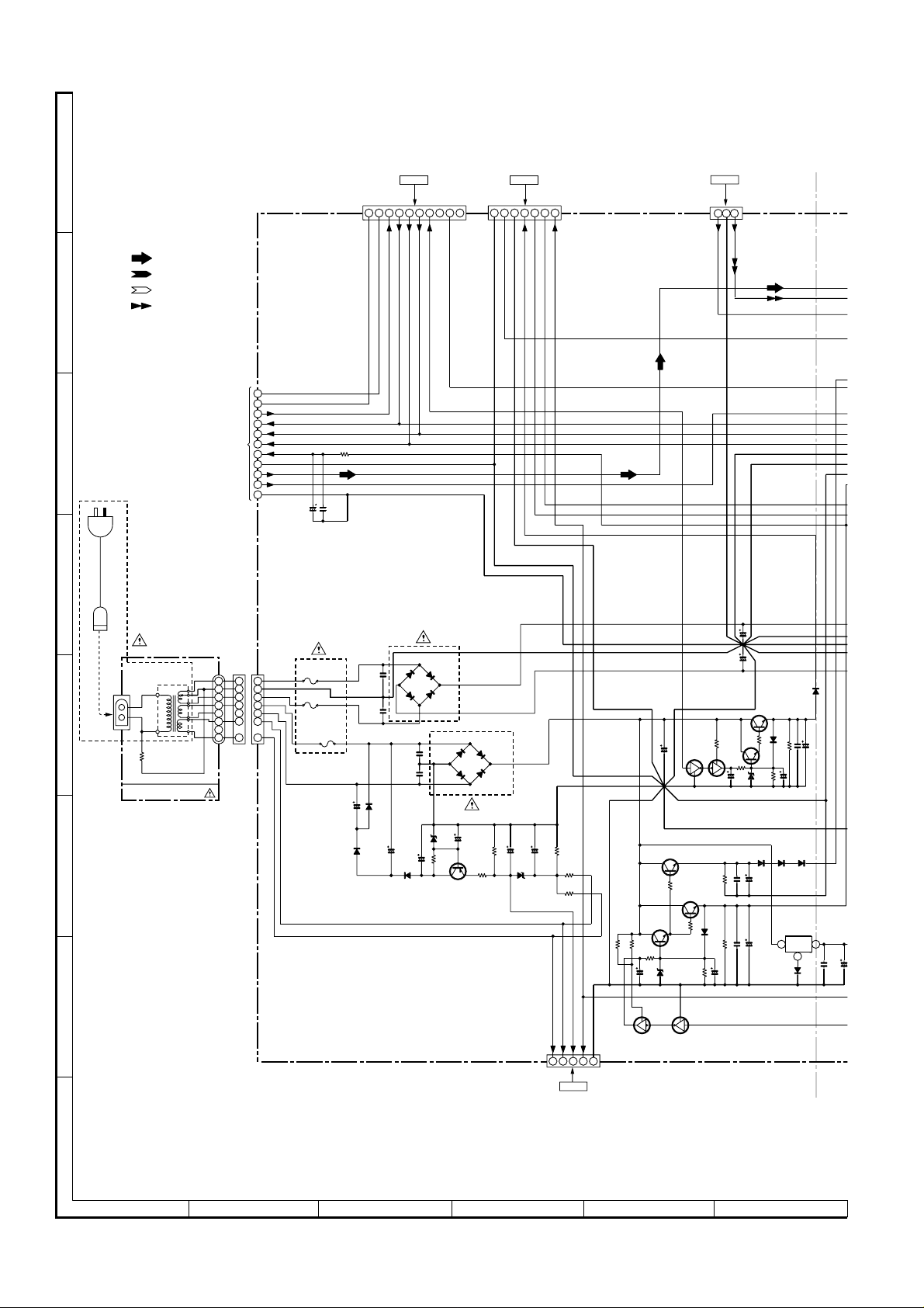
Figure 26 WIRING SIDE OF P.W.BOARD (1/7)
– 26 –
Page 27

CD-XP120
28 2 - B
FROM
ERVO PWB
NS105
5678910
NP105
C101
D101
D102
R106
R105
D116
D107
C204
C203
P28 1 - D
CD SERVO PWB
CNP101
C107
C102
R210
C118
R205
R204
R206
13579
2468
IC201
FROM
CNS101
R101
D103
C110
12
345
CNP102
Q202
R209
ZD203
C117
C202
R203
11 13 15
10 12 14
Q101
ZD101
C108
R104
ZD102
R218
12345678
E
C
B
C109
E C B
C205
R219
D117
C201
R214
P31 11 - D
DISPLAY PWB
R103
R102
ZD201
R207
R208
R217
C207
R220
CNP804
R827
R814
C820
C818
C814
C816
R810
R213
P32 5 - D
TAPE MOTOR
FROM
CNS102
D602
D601
D603
C208
R221
B
C
E
ZD204
4
3
2
CNP803
1
D803
D805
3
2
1
C828
R825
R822
C826
C822
C832
C821
R816
R812
C811
R807
R802
CNP801
FROM
P32 4 - G
FROM TAPE 2
PLAYBACK HEAD
CD SERVO PWB
R215
R216
Q201
3
2
1
R211
CNP103
R834
D802
D804
R838
R836
R835
D806
C830
12 13
10
5
1
C809
C806
R801
3
C802
2
1
C801
C804
P28 1 - B
FROM
CNS103
Q203
B
C
E
R618
C617
C618
R601
B C E
Q204
C837
R833
R837
C840
R829
C833
C834
IC801
C805
C808
R803
R804
FROM TAPE 1
PLAYBACK/RECORD
R613
C620
R603
R623
C615
R610
R201
L801
C836
E C B
Q801
C829
C835
C817
C813
C815
R809
15
20
24
4
3
2
1
C803
P32 3 - H
HEAD
C616
C619
R602
C622
C839
D801
C831
C819
REC./P.B.
C810
R806
CNP802
R805
R622
C623
C612
24
C621
C613
R614
SW801
C812
R625
R621
R202
R611
R615
C614
C601
C608
C610
R605
R607
R609
13
20
15
IC601
510
112
C611
R612
R624
R832
R826
R815
R811
AE
R808
BF
C
DH
C807
C609
R813
C838
R831
C823
C824
C607
R830
C825
C827
G
REC.
P.B.
R608
R606
R604
R820
C606
R620
R617
R828
R821
R819
R619
R616
R818
R817
C604
C605
R824
C602
C603
R823
COLOR TABLE
BROWN
BR
RD(R)
WH(W)
P32 5 - A
FROM
TAPE MECHANISM
OR
YL
GR
BL
VL
GY
BK
PK
RED
ORANGE
YELLOW
GREEN
BLUE
VIOLET
GRAY
WHITE
BLACK
PINK
POWER PWB-A3
R121
AC POWER
SUPPLY CORD
SO101
AC INLET
AC 120 V, 60 Hz
POWER TRANSFORMER
BI104
1
GYGYGYGYGYGYBK
T101
78654321
CNS104
7
8 9 10 11 12
Figure 27 WIRING SIDE OF P.W.BOARD (2/7)
– 27 –
Page 28

CD-XP120
B
C
D
E
F
G
A
P27 9 - A
CNP103
TO MAIN PWB
CNS105
P27 7 - A
TO MAIN PWB
CNP101
CNS101
12345678 123456
BKGYGYGYGYGYGYWHGYGYGYGYGY
D405
BI101
D401
R465
R470
R461
B C E
B C E
R459
R460
D402
R442B
R467
Q412
R471B
Q413
R471A
R468
R481
R463
L405
ZD401
R482
CNP402
1234
WH
1
BK
2
RD
3
CNS103
P26 6 - A
TO MAIN PWB
CNP105
123456789
BKGYGYGYGYGYGYRDWH
P30 1 - C
TO DISPLAY PWB
CNP701
GY
BI701
1186
R478
R477
R475
R476
R479A
R479
IC403
R473
R442A
C422
R434
B
C
Q408
E
Q405
24
25
B
C
E
20
R431
R430
R419
R421
Q406
13
30
36
R452
B
C
E
15
35
12
10
37
B
C
E
Q409
X402
5
45
40
R438
BR
CNS701
1
48
R453
R418
R437
B
C
E
10
BK
GY
GYGYGYGYGY
BI105A
1
C454
R480
L403
RD WH
1
BI105B
R455
R454
R449
R447
R448
C426
Q403
Q402
B
B
C
C
E
E
WH
BK
RD
2
R443
R440
Q411
R441
Q407
R491
C455
C460
7
L404
C452
GYGYGY
3 2 1
R435A
1
3
R498
R499
D406
R435B
D404
D403
E C B
Q410
BI103
R456
R495
R496
R497
BK
14
BI401
R435C
R401
R446
R451
R489A
456
GYGYGYGYGY
R426
C450
C447
C448
R444
R445
20
21
C427
R489B
C425
C415
R422
R415
R425
C449
15
25
C405
C412
C413
231
BI405
C417
R424
C437
10
30
R493
C406
R410
C407
C419
C411
WH
R408
R412
R423
R483
1
5
35
40 41
Q401
R414
C408
CNS405
17
IC404
1
14
R486
C445
R484
80
75
70
55
IC401
50
45
C428
B C E
1
5
10
15
16
IC402
C451
R490
FB402
5
10
R485
C444
65
R458
C404
FB401
C434
30
25
20
C421
25
20
R409
C443
C441
61
60
R462
32
C414
17
28
15
R428
C446
L401
C459
X403
C435
C409
C410
R420
R436
C418
R433
R492
R427
C457
C442
R469
R457
R406
R429
R466
R407
R416
C420
C403
R450
C458
R487
L402
C438
C433
R417
C423
R432
B
C
E
C432
Q404
C416
C401
FB402
R405
9
C436
R474
R402
C431
C402
BI407
R413
1
BI406
R464
8
1
C424
C429
C430
R404
R411
R403
BK
WH
WH
WH
WH
WH
WH
WH
WH
WH
WH
WH
WH
WH
BK
1
2
3
4
5
6
7
8
CNS406
7
6
5
4
3
2
1
CNS407
CD SERVO PWB-A2
GY
4
GY
3
GY
2
BK
1
CNS401
H
1
23456
Figure 28 WIRING SIDE OF P.W.BOARD (3/7)
– 28 –
Page 29

PICKUP UNIT(308)
17
NM802
SPINDLE MOTOR
6
CNP405
SW4
PICKUP IN
12345
F3895AF
B
1
NM801
SLED MOTOR
CD-XP120
COLOR TABLE
BROWN
BR
RD(R)
OR
YL
GR
BL
VL
GY
WH(W)
BK
PK
RED
ORANGE
YELLOW
GREEN
BLUE
VIOLET
GRAY
WHITE
BLACK
PINK
1
8
SWITCH B PWB-A6
SW3
UP
CNP401
1234
SW2
DISC
SW1
OPEN/CLOSE
T/T UP/DOWN
MOTOR PWB-A8
M3
T/T UP/DOWN MOTOR
R919
BI402A
12
CD MOTOR
PWB-C
CD LOADING
MOTOR PWB-A7
CD LOADING MOTOR
BI402B
M1
12
BK
4
RD
3
BL
2
WH
1
CNS402
7
8 9 10 11 12
Figure 29 WIRING SIDE OF P.W.BOARD (4/7)
– 29 –
Page 30

CD-XP120
A
B
P28 2 - D
CNS701
FROM
CD SERVO PWB
C
D
E
SW713
OPEN/
CLOSE
C703
6
5
4
3
2
1
CNP701
RX701
C705
R706
X-BASS/DEMO
R701
1
2
3
C701
R705
C704
SW708
EQUALIZER/
C702
R704
VOLUME UP
R702
12 3456789
SW711
33
34
40
35
44
IC701
5
1
10
11
VFD701
10 11 12 13 14 15 16 17 18 19 20 21 22 23 24 25
SW709
TAPE
SW704
PRESET UP
30
15
12
D704
20
25
23
22
D703
SW707
PRESET
DOWN
D702
SW712
DISC
SKIP
F
SW715
VOLUME DOWN
SW703
TUNING UP
SW706
TUNING
DOWN
G
H
1
23456
Figure 30 WIRING SIDE OF P.W.BOARD (5/7)
– 30 –
Page 31

CD-XP120
22 23 24 25 26 27 28 29 30 31 32 33
SW705
TUNER
(BAND)
D702
D701
DISPLAY PWB-B
R711
R707
SW702
CD
D706
R708
R703
1
BI102
6
1
2
3
CNP702
COLOR TABLE
BR
RD(R)
OR
YL
GR
BL
VL
GY
WH(W)
BK
PK
CNS102
BK
1
GY
2
GY
3
GY
4
GY
5
1
2
3
CNS702
BROWN
RED
ORANGE
YELLOW
GREEN
BLUE
VIOLET
GRAY
WHITE
BLACK
PINK
P27 8 - A
CNP102
TO MAIN PWB
BK
WH
W707
RESET
OWN
W706
UNING
OWN
12
BI702
SW701
ON/STAND-BY
SW714
PLAY/REPEAT
C707
C706
SW710
STOP
SWITCH A PWB-A5
7
8 9 10 11 12
Figure 31 WIRING SIDE OF P.W.BOARD (6/7)
– 31 –
Page 32

CD-XP120
A
B
YL
RD
RD
RD
YL
OR
RD
BR
4
3
2
1
P27 10 - D
CNP803
TO MAIN PWB
SW5
TAPE 1
PLAY
SW6
TAPE 1
FF/REW
SW7
TAPE 2
FF/REW
SW8
TAPE 2
PLAY
C
M2
TAPE
MOTOR
A
B
+
-
WH
BK
3
2
1
P27 8 - G
CNP804
TO MAIN PWB
D
E
ERASE
HERAD
TAPE 1 TAPE 2
RECORD/PLAYBACK
HEAD
PLAYBACK
HEAD
WH
F
RD
G
H
TO MAIN PWB
1
23456
RD
BK
WH
CNP802
P27 9 - G
BK
4321
BK
BK
WH
RD
BK
BR
WH
BK
RD
23
1
CNP801
P27 8 - H
TO MAIN PWB
COLOR TABLE
BROWN
BR
RD(R)
OR
YL
GR
BL
VL
GY
WH(W)
BK
PK
RED
ORANGE
YELLOW
GREEN
BLUE
VIOLET
GRAY
WHITE
BLACK
PINK
Figure 32 WIRING SIDE OF P.W.BOARD (7/7)
– 32 –
Page 33

VOLTAGE
CD-XP120
IC101
PIN
VOLTAGE
NO.
1 18 V
0.6 V
2
3
4.9 V
IC201
PIN
VOLTAGE
NO.
1 0.14 V
22 V
2
3
0.15 V
–22 V
4
0 V
5
0.3 V
6
0 V
7
0 V
8
0 V
9
10 0 V
11 0.3 V
12 0 V
13 0 V
14 0 V
15 22 V
IC402
PIN
VOLTAGE
NO.
10 V
4.2 V
2
3
5.1 V
2.7 V
4
2.4 V
5
4.3 V
6
1.7 V
7
2.7 V
8
3.5 V
9
10 2.7 V
11 4 V
12 0 V
13 3.8 V
14 0 V
15 0 V
16 0 V
17 2.7 V
18 0 V
19 2.7 V
20 2.7 V
21 2.7 V
22 2.7 V
23 2.7 V
24 3.1 V
25 2.7 V
2.7 V
26
27
2.7 V
2.7 V
28
2.8 V
29
2.8 V
30
2.8 V
31
2.8 V
32
PIN
VOLTAGE
NO.
1 2.6 V
2.6 V
2
3
2.6 V
5.1 V
4
0 V
5
2.5 V
6
4.5 V
7
4 V
8
4.7 V
9
10 0 V
11 0 V
12 0 V
13 0 V
14 5.1 V
15 2.5 V
16 0.2 V
17 0.3 V
18 4.8 V
19 2.6 V
20 2.6 V
21 2.7 V
22 2.7 V
23 2.7 V
24 2.7 V
25
2.7 V
26
2.7 V
27
2.7 V
28
2.7 V
29
2.7 V
30
2.4 V
2.4 V
31
32
2.7 V
33
2.7 V
34
2.7 V
35
0.3 V
36
0.3 V
37
2.3 V
38
0.3 V
39
0.3 V
40
5 V
Q101
PIN
VOLTAGE
NO.
E –27 V
–28 V
C
B
–23 V
Q102
PIN
VOLTAGE
NO.
E 12 V
18 V
C
B
12.5 V
Q103
PIN
VOLTAGE
NO.
E 11.4 V
18.6 V
C
B
12 V
IC401
PIN
VOLTAGE
NO.
41 0.2 V
2.7 V
42
43
0 V
2.7 V
44
1.3 V
45
0.5 V
46
2.7 V
47
1.6 V
48
0.3 V
49
50 5.1 V
51 0.3 V
52 2.7 V
53 2.7 V
54 0.2 V
55 0.3 V
56 5 V
57 0.3 V
58 2.5 V
59 2.7 V
60 5.1 V
61 4.8 V
62 0.3 V
63 0.3 V
64 0.2 V
65
0.3 V
66
5.1 V
67
5.1 V
68
0.3 V
69
5.1 V
70
5.1 V
5.1 V
71
72
4.7 V
73
2.4 V
74
0.3 V
75
2.4 V
76
5.1 V
77
0.2 V
78
0.2 V
79
5.1 V
80
5.1 V
Q104
PIN
VOLTAGE
NO.
E 11.3 V
18.5 V
C
B
12 V
Q105
PIN
VOLTAGE
NO.
E 7.9 V
18.5 V
C
B
9.3 V
Q106
PIN
VOLTAGE
NO.
E 6.8 V
18.5 V
C
B
7.9 V
IC403
PIN
VOLTAGE
NO.
1 4.8 V
0 V
2
3
0 V
0 V
4
0 V
5
0 V
6
0 V
7
5 V
8
0 V
9
10 0 V
11 0 V
12 4.8 V
13 0 V
14 4.8 V
15 2.4 V
16 2.3 V
17 0 V
18 2 V
19 2.4 V
20 4.8 V
21 4.8 V
22 4.8 V
23 0 V
24 5 V
25
4.9 V
26
2.4 V
27
4.6 V
28
4.6 V
29
4.8 V
30
4.8 V
4.8 V
31
32
0 V
33
4.8 V
34
4.8 V
35
4.8 V
36
5.1 V
37
4.9 V
38
0 V
39
0 V
40
0 V
41
4.8 V
42
4.8 V
43
4.8 V
44
0 V
45
0.2 V
46
4.6 V
47
4.1 V
48
4.8 V
IC404
PIN
VOLTAGE
NO.
1 2.7 V
2.7 V
2
3
2.7 V
2.7 V
4
5.2 V
5
5.2 V
6
4.7 V
7
0 V
8
2.7 V
9
10 2.7 V
11 2.4 V
12 2.9 V
13 0 V
14 2.9 V
15 0 V
16 5.6 V
17 2.7 V
18 2.7 V
19 2.7 V
20 2.7 V
21 6 V
22 6 V
23 2.7 V
24 2.7 V
25 2.7 V
3 V
26
27
2.5 V
0 V
28
2.7 V
29
2.9 V
30
2.4 V
31
0 V
32
IC601
PIN
VOLTAGE
NO.
1 4.8 V
0 V
2
3
0 V
4.8 V
4
4.8 V
5
4.8 V
6
4.8 V
7
4.8 V
8
4.8 V
9
10 4.8 V
11 4.8 V
12 4.8 V
13 4.8 V
14 4.8 V
15 4.8 V
16 4.8 V
17 4.8 V
18 4.8 V
19 4.8 V
20 4.8 V
21 4.8 V
22 4.8 V
23 9.4 V
24 4.8 V
IC701
PIN
VOLTAGE
NO.
10 V
0 V
2
3
0 V
0 V
4
4.4 V
5
4.4 V
6
0 V
7
4.5 V
8
4.8 V
9
10 0 V
11 0 V
12 0 V
13 0 V
14 5.2 V
15 3.5 V
16 8.3 V
17 13.2 V
18 16.2 V
19 16.2 V
20 13.2 V
21 17.6 V
22 –27 V
23 –25 V
24 –27 V
25
15.2 V
26
7.2 V
27
–28 V
28
12.5 V
29
7.2 V
30
4.4 V
3.8 V
31
32
7.2 V
33
7.2 V
34
4.3 V
35
7.2 V
36
7.2 V
37
7.2 V
38
4.7 V
39
4.8 V
40
4.8 V
41
4.8 V
42
4.8 V
43
0 V
44
2.6 V
Q109
PIN
VOLTAGE
NO.
E 9.4 V
9.4 V
C
B
0 V
Q110
PIN
VOLTAGE
NO.
E0 V
0 V
C
B
4.8 V
IC801
PIN
VOLTAGE
NO.
10 V
1.5 V
2
3
1.5 V
1.8 V
4
0.8 V
5
0 V
6
0 V
7
0.6 V
8
3 V
9
10 3 V
11 0 V
12 0 V
13 6.2 V
14 3.8 V
15 0 V
16 3 V
17 0.6 V
18 0 V
19 0 V
20 1 V
21 1.8 V
22 0.6 V
23 0 V
24 0 V
Q111
PIN
VOLTAGE
NO.
E0 V
0 V
C
B
4.3 V
Q112
PIN
VOLTAGE
NO.
E 9.4 V
9.4 V
C
B
0 V
Q201
PIN
VOLTAGE
NO.
E0 V
0 V
C
B
0.7 V
Q202
PIN
VOLTAGE
NO.
E0 V
0 V
C
B
0.7 V
Q203
PIN
VOLTAGE
NO.
E0 V
0 V
C
B
0.6 V
Q204
PIN
VOLTAGE
NO.
E0 V
0 V
C
B
0.6 V
Q351
PIN
VOLTAGE
NO.
E0 V
4.7 V (0 V)
C
B
3.7 V (0 V)
Q401
PIN
VOLTAGE
NO.
E5 V
2.1 V
C
B
4.2 V
Q402
PIN
VOLTAGE
NO.
E0 V
0.3 V
C
B
0 V
Q403
PIN
VOLTAGE
NO.
E 5.7 V
0 V
C
B
5.3 V
Q404
PIN
VOLTAGE
NO.
E 6.3 V
5.2 V
C
B
5.2 V
Q405
PIN
VOLTAGE
NO.
E0 V
5.3 V
C
B
0 V
Q406
PIN
VOLTAGE
NO.
E0 V
5.3 V
C
B
0 V
Q407
PIN
VOLTAGE
NO.
E6 V
3 V
C
B
5.5 V
Q408
PIN
VOLTAGE
NO.
E0 V
0.3 V
C
B
0 V
Q412
PIN
VOLTAGE
NO.
E0 V
4.8 V
C
B
0 V
Q413
PIN
VOLTAGE
NO.
E0 V
0 V
C
B
1.1 V
Q801
PIN
VOLTAGE
NO.
E 0.26 V
4.92 V
C
B
0.94 V
– 33 –
Page 34

CD-XP120
NOTES ON SCHEMATIC DIAGRAM
• Resistor:
To differentiate the units of resistors, such symbol as K and
M are used: the symbol K means 1000 ohm and the symbol
M means 1000 kohm and the resistor without any symbol is
ohm-type resistor. Besides, the one with “Fusible” is a fuse
type.
• Capacitor:
To indicate the unit of capacitor, a symbol P is used: this
symbol P means pico-farad and the unit of the capacitor
without such a symbol is microfarad. As to electrolytic
capacitor, the expression “capacitance/withstand voltage”
is used.
(CH), (TH), (RH), (UJ): Temperature compensation
(ML): Mylar type
(P.P.): Polypropylene type
• Schematic diagram and Wiring Side of P.W.Board for this
model are subject to change for improvement without prior
notice.
• The indicated voltage in each section is the one measured
by Digital Multimeter between such a section and the chassis with no signal given.
1. In the tuner section,
indicates AM
indicates FM stereo
2. In the main section, a tape is being played back.
3. In the deck section, a tape is being played back.
( ) indicates the record state.
4. In the power section, a tape is being played back.
5. In the CD section, the CD is stopped.
• Parts marked with “ 1 ” ( ) are important for
maintaining the safety of the set. Be sure to replace these
parts with specified ones for maintaining the safety and
performance of the set.
REF. NO DESCRIPTION POSITION
SW1 OPEN/CLOSE ON—OFF
SW2 DISC ON—OFF
SW3 UP ON—OFF
SW4 PICKUP IN ON—OFF
SW5 TAPE 1 PLAY ON—OFF
SW6 TAPE 1 FF/REW ON—OFF
SW7 TAPE 2 FF/REW ON—OFF
SW8 TAPE 2 PLAY ON—OFF
SW701 ON/STAND-BY ON—OFF
SW702 CD ON—OFF
SW703 TUNING UP ON—OFF
SW704 PRESET UP ON—OFF
TYPES OF TRANSISTOR
FRONT
VIEW
REF. NO
SW705 TUNER (BAND) ON—OFF
SW706
SW707 PRESET DOWN ON—OFF
SW708 EQUALIZER/X-BASS/DEMO ON—OFF
SW709 TAPE ON—OFF
SW710 STOP ON—OFF
SW711 VOLUME UP ON—OFF
SW712 DISC SKIP ON—OFF
SW713 OPEN/CLOSE ON—OFF
SW714 PLAY/REPEAT ON—OFF
SW715 VOLUME DOWN ON—OFF
SW801 REC./P.B. ON—OFF
TUNING DOWN
DESCRIPTION
POSITION
ON—OFF
FRONT
VIEW
E C B
(S) (G) (D)
(1) (2) (3)
KRA102 M
KRC102 M
KRC107 M
KRC104 M
KSA1015 GR
HSB562 C
HSC1609 GR
KSC1815 GR
KSC3203 Y
KSA1271 Y
SSC1674 C
B C E
2SD2012 Y
– 34 –
Page 35

FUNCTION T ABLE OF IC
IC402 VHiAN22000A-1: Head Amp. (AN22000A)
Pin No. FunctionTerminal Name
1 PD APC amp input.
2 LD APC amp output.
3 VCC Power supply.
4 RFN RF amp inverting input.
5 RFOUT RF addition amp output.
6 RFIN AGC amp input.
7 CAGC AGC loop filter connection.
8 ARF AGC output.
9 CEA Capacitor for HPF-amp connection.
10 3TOUT 3T-ENV output.
11 CBDO Capacitor for RF dark-side envelope detection connection.
12 BDO BDO output.
13 COFTR Capacitor for RF bright-side envelope detection connection.
14 OFTR OFTR output.
15 NRFDET NRFDET output.
16 GND Ground
17 VREF VREF output.
18 VDET VDET output.
19 TEBPF VDET input.
20 TEOUT TE amp output.
21 TEN TE amp inverting input.
22 FEN FE amp inverting input.
23 FEOUT FE amp output.
24 GCTL Gain & APC control.
25 FBAL FBAL control.
26 TBAL TBAL control.
27 E Tracking signal input 1.
28 F Tracking signal input 2.
29 D Focus signal input 4.
30 B Focus signal input 2.
31 C Focus signal input 3.
32 A Focus signal input 1.
CD-XP120
OFTR
COFTR
BD0
CBD0
ARF
CAGC
RFIN
RFOUT
RFN
3TOUT
CEA
10915
14
OFTR
13
12
11
8
7
6
5
4
3TENV
BDO
AGC
NRFDET
RF_EQ
NRFDET
FEN
FEOUT
TEN
TEOUT
BCA
GCA
AMP
B
20
-
+
SUBT
BCA
GCA
AMP
27293031
E
D
22 23 21
-
+
SUBT
BCA
GCA
AMP
32 28
A
C
TEBPF
19
BCA
GCA
AMP
F
18
VDET
VDET
+
17
LD
2
-
+
-
VREF
PD
1
VCC
3
GND
16
25
FBAL
26
TBAL
24
GCTL
Figure 35 BLOCK DIAGRAM OF IC
– 35 –
Page 36

CD-XP120
IC401 VHiMN6627482W: CD Signal Control (MN6627482WA) (1/2)
Terminal NamePin No. Input/Output
1* BCLK Output SRDATA bit clock output.
2* LRCK Output L/R identification signal output.
3* SRDATA Output Serial data output.
4 DVDD1 Input Digital circuit power supply.
5 DVSS1 Input Digital circuit GND.
6* TX Output Digital audio interface output signal.
7 MCLK Input Microcomputer command clock signal input. (Data latch at the rising edge.)
8 MDATA Input Microcomputer command data input.
9 MLD Input Microcomputer command load signal input. L: Load
10* SENSE Output Sense signal output. (OFT, FESL, NACEND, NAJEND, SFG)
11* /FLOCK Output Focus servo lead-in signal. (L: Lead-in)
12* /TLOCK Output Tracking servo lead-in signal. (L: Lead-in)
13 BLKCK Output Subcode block clock signal. (fBLKCK=75 Hz)
14 SQCK, GIO0 Input Default: external clock input for subcode Q resistor.
Command execution: general purpose I/O port.
CD-TEXT mode 2: TEXT data read clock input.
15* SUBQ Output Subcode Q data output.
CD-TEXT mode 2: TEEXT data output.
16 DMUTE Input Muting input. (Effective only at bit rate 64fs output.) H: Mute
17 STAT Output Status signal. (CRC, STCNT, CLVS, TTSTOP, JCLVS, SQOK, FLAG6, SENE, FLOCK,
TLOCK, revolving speed data, FCLV, SUBQ, SYFLG)
CD-TEXT mode 3: subcode Q and TEXT data output.
18 /RST Input Reset input (L: Reset)
19* SMCK Output MSEL=H: 8.4672 MHz clock signal output.
MSEL=L: 4.2336 MHz clock signal output.
20* PMCK, PLAY Output Default: 88.2 kHz clock signal output.
Command execution: Play signal output. H: play
21 TRV Output Traverse forcing transmission output. 3-State
22 TVD Output Traverse drive output.
23* PC Output Spindle motor ON output. L: ON (Default)
24 ECM Output Spindle motor drive signal. (Forcing mode output.) 3-State
25 ECS Output Spindle motor drive signal. (Servo error signal output.)
26 KICK Output Kick pulse output. 3-State
27 TRD Output Tracking drive output.
28 FOD Output Focus drive output.
29 VREF Input DA output section (TVD, ECS, TRD, FOD, FBAL, TBAL, TOFS) reference voltage.
30 FBAL Output Focus balance adjustment output.
31 TBAL Output Tracking balance adjustment output.
32 FE Input Focus error signal input. (Analog input)
33 TE Input Tracking error signal input. (Analog input)
34 RFENV Input RF envelope signal input. (Analog input)
35 VDET Input Oscillation detection signal input. H: Detection
36 OFT Input Off track signal input. H: Off track
37 TRCRS Input Track cross signal input. (Analog input)
38 /RFDET Input RF detection signal input. L: Detection
39 BDO Input Drop out signal input. H: Drop out
40 LDON Output Laser ON signal output. H: ON
41 PLLF2 Input/Output Loop filter characteristic switch terminal for PLL.
42* TOFS Output Tracking offset adjustment output. (Shared with general purpose DA output terminal.)
43* WVEL Output Double-speed status signal output. H: Double-speed
44 ARF Input RF signal input.
45 IREF Input Reference current input terminal
46* DRF Input DSL bias terminal.
In this unit, the terminal with asterisk mark (*) is (open) terminal which is not connected to the outside.
Function
– 36 –
Page 37

IC401 VHiMN6627482W: CD Signal Control (MN6627482WA) (2/2)
Terminal NamePin No. Input/Output
47 DSLF Input/Output DSL loop filter terminal.
48 PLLF Input/Output PLL loop filter terminal.
49 VCOF Input/Output VCO loop filter terminal.
50 AVDD2 Input Analog circuit power supply. (DSL, PLL and DA output sections for AD)
51 AVSS2 Input Analog circuit GND. (DSL, PLL and DA output sections for AD)
52* EFM, CK384 Output · IOSEL=H: EFM signal output.
· IOSEL=L: X-tal system 16.9344 MHz clock output.
Signal processing system: 384fs output. (VCO clock for jitter-free operation)
(X-tal system or signal processing system can be selected by the command.)
53 PCK, DSLB Output PLL extraction clock output or DSL balance output. fPCK-4.3218 MHz
54 VCOF2 Input/Output Loop filter terminal for digital servo 33.8688 MHz creation VCO.
X-tal 16.9344 MHz: external circuit is needed.
55* SUBC Output Subcode serial output. CD-TEXT mode 1: TEXT data output.
56* SBCK Input Subcode serial output clock input. CD-TEXT mode 1: TEXT data read clock input
57 VSS Input Oscillation circuit GND.
58 X1 Input Oscillation circuit input terminal. f=16.9344 MHz, 33.8688 MHz
59 X2 Output Oscillation circuit output terminal. f=16.9344 MHz, 33.8688 MHz
60 VDD Input Oscillation circuit power supply.
61* BYTCK, TRVSTP Output IOSEL=H: byte clock signal output.
IOSEL=L: traverse STOP signal output. H: STOP Mode
62* GIO1, /CLDCK Output Default: general purpose I/O port.
Command execution: terminal for subcode frame clock signal output. (fCLDCK=7.35 kHz)
63* GIO2, FCLK Output Default: general purpose I/O port.
Command execution: crystal frame clock signal output. (fFCLK=7.35 kHz)
64* IPFLAG Output Interpolation flag signal output. H: Interpolation
65* FLAG Output Flag signal output.
66* CLVS Output Output for spindle servo phase synchronization signal. H: CLV, L: Rough servo
67* CRC Output Default: output for subcode CRC check results. H: OK, L: NG
68* DEMPH Output Demphasis detection signal output. H: ON
69* RESY, FLAG6 Output IOSEL= H: resync signal RESY output for frame synchronization.
H: Synchronization, L: Synchronization lost
IOSEL=L: RAM address reset signal for error correct deinterleave.
FLAG 6 output L: Address reset
70 IOSEL Input Mode switch terminal.
71 /TEST Input Test terminal. Normal: H
72 AVDD1 Input Analog circuit power supply. (Audio output section (for both Lch and Rch))
73 OUTL Output Lch audio output.
74 AVSS1 Input Analog circuit GND. (Audio output section (for both Lch and Rch))
75 OUTR Output Rch audio output.
76 RSEL, GIO3 Input Default: RF signal polarity specification terminal.
Brightness H: RESEL=H Brightness L: RESEL=L
Command execution: general purpose I/O port.
RF signal polarity can be specified by command.
CD-TEXT mode 1 or 2: TEXT data read enabling signal (DQSY) output
77 CSEL Input Oscillation frequency specification terminal.
H: Oscillation frequency=33.8688 MHz L: Oscillation frequency=16.9344 MHz
78 PSEL Input IOSEL=H: test terminal. (Normal: L)
IOSEL=L: SRDATA input.
79 MSEL Input IOEL=H: SMCK terminal output, frequency switch terminal.
H: SMCK=8.4672 MHz L: SMCK=4.2336 MHz
IOSEL=L: LRCK input
H: Lch data, L: Rch data
SMCK=4.2336 MHz fixed
80 SSEL Input IOSEL=H: switch terminal for SUBQ terminal output mode.
H: Q code buffer mode L: CLDCK synchronization mode
IOSEL=L: BCLK input
Q code buffer mode fixed
In this unit, the terminal with asterisk mark (*) is (open) terminal which is not connected to the outside.
Function
CD-XP120
– 37 –
Page 38

CD-XP120
IC401 VHiMN6627482W: CD Signal Control (MN6627482WA)
V
DD
V
SS
DV
DD1
DV
SS1
/RST
/TEST
FE
TE
RFENV
TRCRS
VDET
BDO
/RFDET
OFT
STATX1X2
TIMING
GENERATOR
PITCH CONTROL
A/D CONVERTER
INPUT PORT
SERVO
TIMING
GENERATOR
MSEL
CSEL
PMCK(PLAY)
GIO2(FCLK)
SMCK
BYTCK(TRVSTP)
VCO
MICRO
COMPUTER
INTERFACE
SERVO
CPU
OUTPUT PORT
D/A
CONVERTER
VCOF
VCOF2
MDATA
MCLK
MLD
REF
PSEL
RSEL(GIO3)
ARF
DRF
I
DSLF
PLLF2
DSL • PLL VCO
EFM DEMODULATION
SYNC INTERPOLATION
DD2AVSS2
PLLF
EFM(CK384)
PCK(DSLB)
AV
SUBCODE
BUFFER
SUBQ
SOCK(GIO0)
CD-TEXT
BUFFER
SUBCODE DEMODULATION
CIRC ERROR CORRECTION
DEINTERLEAVE
INTER
POLATION
SOFT MUTING
DIGITAL
CLV
SERVO
INTERFACE
ATTENUATION
SSEL
FLAG6(RESY)
16k
SRAM
DIGITAL
AUDIO
DEMPH
SUBC
SBCK
GIO1(/CLDCK)
BLKCK
CRC
CLVS
IOSEL
+
SRDATAIN(PSEL)
BCLKIN(SSEL)
DIGITAL
DEEMPHSIS
8TIMES
OVER
SAMPLING
DIGITAL FILTER
1 BIT DAC
PWMLOGIC
PWM
(L)
-
LRCKIN(MSEL)
PWM
(R)
-
+
WVEL
SENSE
LDON
/FLOCK
FBAL
TBAL
/TLOCK
TVD
TRV
TRD
FOD
VREF
KICK
TOFS
BCLK
DMUTE
LRCK
SRDATA
Figure 38 BLOCK DIAGRAM OF IC
PC
ECS
ECM
TX
FLAG
IPFLAG
OUTL
SS1
DD1
AV
OUTR
AV
– 38 –
Page 39

VFD701 VVK250808//-1
CD-XP120
FL DISPLAY
1G 2G
1
2
3
SLEEP
PIN NO. 123456789101112131415161718
CONNECTION F
PIN NO.
CONNECTION
REC
FM
AM
19
P1
F
20
P2
NP
21
P3
3G 4G 5G 6G 7G 8G
6G
27
P9
7G
28
P10
8G
8G
29
P11
NC
NC NC NC NC NC NC
30
31
P12
P1332P1433NP34F
f
g
e
( )
2G-7G
1G
2G
22
23
P4
P5
a
k
j
h
r
i
d
3G
4G
24
25
P6
P7
b
m
n
c
5G
26
P8
P1
P2
P3
P4
P5
P6
P7
P8
P9
P10
P11
P12
1G
3
2
1
FM
AM
REC
(Left)
SLEEP
2G 3G 4G 5G 6G 7G 8G
k
h
f
b
a
g
m
r
j
n
c
e
k
h
f
b
a
g
m
r
j
n
c
e
k
h
f
b
a
g
m
r
n
c
e
k
h
f
b
a
g
m
r
j
j
n
c
e
k
h
f
b
a
g
m
r
j
n
c
e
k
h
f
b
a
g
m
r
j
n
c
e
P13
P14
(Right)
d
d
d
– 39 –
d
d
d
Page 40

CD-XP120
— M E M O —
– 40 –
Page 41

PARTS GUIDE
MINI COMPONENT SYSTEM
MODEL CD-XP120
CD-XP120 Mini Component System consisting of CD-XP120
(main unit) and CP-XP120 (speaker system).
CD-XP120
“HOW TO ORDER REPLACEMENT PARTS”
To have your order filled promptly and correctly, please furnish the
following information.
1. MODEL NUMBER 2. REF. No.
3. PART NO. 4. DESCRIPTION
MARK: SPARE PARTS-DELIVERY SECTION
Explanation of capacitors/resistors parts codes
Capacitors
VCC ....................... Ceramic type
VCK........................ Ceramic type
VCT........................ Semiconductor type
VC • • MF............... Cylindrical type (without lead wire)
VC • • MN............... Cylindrical type (without lead wire)
VC • • TV................ Square type (without lead wire)
VC • • TQ ............... Square type (without lead wire)
VC • • CY ............... Square type (without lead wire)
VC • • CZ ............... Square type (without lead wire)
VC • • • • • • • • • J .. The 13th character represents capacity difference.
("J" ±5%, "K" ±10%, "M" ±20%, "N" ±30%,
"C" ±0.25 pF, "D" ±0.5 pF, "Z" +80-20%.)
If there are no indications for the electrolytic capacitors, error is ±20%.
For U.S.A. only
Contact your nearest SHARP Parts Distributor to order.
For location of SHARP Parts Distributor,
Please call Toll-Free;
1-800-BE-SHARP
Resistors
VRD ....................... Carbon-film type
VRS........................ Carbon-film type
VRN ....................... Metal-film type
VR • • MF ............... Cylindrical type (without lead wire)
VR • • MN............... Cylindrical type (without lead wire)
VR • • TV................ Square type (without lead wire)
VR • • TQ ............... Square type (without lead wire)
VR • • CY ............... Square type (without lead wire)
VR • • CZ ............... Square type (without lead wire)
VR • • • • • • • • • J .. The 13th character represents error.
("J" ±5%, "F" ±1%, "D" ±0.5%.)
If there are no indications for other parts, the resistors are ±5%
carbon-film type.
CAUTION:FOR CONTINUED
PROTECTION AGAINST FIRE
HAZARD, REPLACE ONLY WITH
SAME TYPE F101, F102 3.15A, 125V /
F103 1.6A, 125V FUSES
ATTENTION:POUR ASSURER
UNE LONGUE PROTECTION CONTRE
UNINCENDIE, REMPLACER SEULEMENT
PAR UN FUSIBLE DE
TYPE F101, F102 3.15A, 125V /
F103 1.6A, 125V
NOTE:
Parts marked with “ ” are important for maintaining the safety of the set.
Be sure to replace parts with specified ones for maintaining the safety and performance of the set.
Page 42

CD-XP120
PRICE
RANK
DESCRIPTIONNO. PART CODE NO. PARTS CODE
CD-XP120
INTEGRATED CIRCUITS
IC101 VHIMC7805CT-1 J AF Voltage Regulator,MC7805CT
IC201 VHILM1876TF-1 J BD Power Amp.,LM1876TF
IC301 VHITA7358AP-1 J AG FM Front End,TA7358AP
IC302 VHILC72131/-1 J AP PLL (Tuner),LC72131
IC303 VHILA1832S/-1 J AN FM IF Det./FM Mpx./AM IF,
IC401 VHIMN6627482W J AV CD Signal Control,MN6627482W
IC402 VHIAN22000A-1 J AF Head Amp.,AN22000A
IC403 RH-IX0051SJZZ J System Microcomputer,
IC404 VHIMM1469XH-1 J AN Focus/Tracking/Spin/Sled Driver,
IC601 VHILC75341M-1 J AM Audio Processor,LC75341M
IC701 VHISC16312/-1 J BD System Microcomputer,SC16312
IC801 VHIAN7345K/-1 J AM Playback and Record/Playback
LA1832S
IX0051SJ
MM1469XH
Amp.,AN7345K
TRANSISTORS
Q101 VSKSA1015GR-1 J Silicon,PNP,KSA1015 GR
Q102 VSHSC1609GR-1 J Silicon,NPN,HSC1609 GR
Q103,104 VS2SD2012Y/-1 J AF Silicon,NPN,2SD2012 Y
Q105 VSHSC1609GR-1 J Silicon,NPN,HSC1609 GR
Q106 VS2SD2012Y/-1 J AF Silicon,NPN,2SD2012 Y
Q109 VSKRA102M//-1 J AC Digital,PNP,KRA102 M
Q110,111 VSKRC107M//-1 J AC Digital,NPN,KRC107 M
Q112 VSKRA102M//-1 J AC Digital,PNP,KRA102 M
Q201 VSKSC1815GR-1 J Silicon,NPN,KSC1815 GR
Q202 VSHSC1609GR-1 J Silicon,NPN,HSC1609 GR
Q203,204 VSKSC1815GR-1 J Silicon,NPN,KSC1815 GR
Q302 VSSC1674-C/-1 J Silicon,NPN,SSC1674 C
Q306 VSSC1674-C/-1 J Silicon,NPN,SSC1674 C
Q351 VSKRC104M//-1 J AC Digital,NPN,KRC104 M
Q360 VSKSA1015GR-1 J Silicon,PNP,KSA1015 GR
Q401 VSKSA1015GR-1 J Silicon,PNP,KSA1015 GR
Q402 VSKSC3203Y/-1 J Silicon,NPN,KSC3203 Y
Q403 VSKSA1271Y/-1 J Silicon,PNP,KSA1271 Y
Q404 VSHSB562-C/-1 J Silicon,PNP,HSB562 C
Q405,406 VSKSC1815GR-1 J Silicon,NPN,KSC1815 GR
Q407 VSKSA1271Y/-1 J Silicon,PNP,KSA1271 Y
Q408 VSKSC3203Y/-1 J Silicon,NPN,KSC3203 Y
Q409 VSKSC1815GR-1 J Silicon,NPN,KSC1815 GR
Q410 VSKSA1271Y/-1 J Silicon,PNP,KSA1271 Y
Q411 VSKRC102M//-1 J AC Digital,NPN,KRC102 M
Q412,413 VSKSC1815GR-1 J Silicon,NPN,KSC1815 GR
Q801 VSKSC3203Y/-1 J Silicon,NPN,KSC3203 Y
DIODES
D101~103 VHD1N4004//-1 J AB Silicon,1N4004
D104 VHD1N4148//-1 J AA Silicon,1N4148
D105 VHD1N4004//-1 J AB Silicon,1N4004
D106 VHD1N4148//-1 J AA Silicon,1N4148
D107 VHD1N4004//-1 J AB Silicon,1N4004
1 D108~111 VHD1N5402M/-1 J AE Silicon,1N5402M
1 D112~115 VHD1N4004//-1 J AB Silicon,1N4004
D116,117 VHD1N4004//-1 J AB Silicon,1N4004
D119 VHD1N4004//-1 J AB Silicon,1N4004
D301,302 VHD1N4148//-1 J AA Silicon,1N4148
D305~308 VHD1N4148//-1 J AA Silicon,1N4148
D401 VHD1N4148//-1 J AA Silicon,1N4148
D402,403 VHD1N4004//-1 J AB Silicon,1N4004
D404~406 VHD1N4148//-1 J AA Silicon,1N4148
D601~603 VHD1N4004//-1 J AB Silicon,1N4004
D701~704 VHD1SS133//-1 J AA Silicon,1SS133
D706 VHD1N4004//-1 J AB Silicon,1N4004
D801 VHD1N4004//-1 J AB Silicon,1N4004
D802~806 VHD1N4148//-1 J AA Silicon,1N4148
ZD101 VHEDZ300BSB-1 J AB Zener,30V,DZ30BSB
ZD102 VHEDZ6R2BSA-1 J AB Zener,6.2V,DZ6.2BSA
ZD103 VHEDZ130BSA-1 J AC Zener,13V,DZ13BSA
ZD104 VHEDZ8R2BSC-1 J AB Zener,8.2V,DZ8.2BSC
ZD201 VHEDZ3R3BSB-1 J AB Zener,3.3V,DZ3.3BSB
ZD203,204 VHEDZ3R3BSB-1 J AB Zener,3.3V,DZ3.3BSB
ZD351 VHEDZ5R1BSB-1 J AC Zener,5.1V,DZ5.1BSB
ZD401 VHEDZ3R3BSB-1 J AB Zener,3.3V,DZ3.3BSB
PRICE
RANK
DESCRIPTION
FILTERS
BF301 RFILR0008AWZZ J AE Band Pass Filter
CF302,303 RFILF0004SJZZ J AG FM IF,10.7 MHz
CF351 RFILF0003AWZZ J AK FM IF
CF352 RFILA0003SJZZ J AF AM IF
TRANSFORMERS
1 T101 RTRNP0079SJZZ J AX Power [Except for Canada]
1 T101 RTRNP0089SJZZ J Power [For Canada]
T302 RCILA0007SJZZ J AG AM Antenna
T304 RCILI0005SJZZ J AF FM IF
T306 RCILB0009SJZZ J AG AM OSC.
T351 RCILI0004SJZZ J AF AM IF
COILS
L101,102 RCILZ0024AWZZ J AC 3 µH,Choke
L103 VP-DH100K0000 J AB 10 µH,Choke
L302 RCILR0003SJZZ J AD FM RF
L303 RCILB0016SJZZ J FM OSC.
L351,352 VP-DH101K0000 J AB 100 µH,Choke
L353 VP-DH102K0000 J AB 1 mH,Choke
L401,402 VP-DHR82K0000 J AE 0.82 µH,Choke
L403~405 VP-DH2R2K0000 J AB 2.2 µH,Peaking
L801 RCILB0003SJZZ J AD OSC,Bias
FB401~403 RCORF0010SJZZ J Coil
VARIABLE RESISTOR
VR351 RVR-M0026AWZZ J AC 10 kohm (B),Semi-VR [FM Mute
Level]
VARIABLE CAPACITORS
VD301 VHCSVC348S/-1 J AK Variable Capacitance,SVC348S
VD302,303 VHCKDV147B/-1 J AH Variable Capacitance,KDV147B
VIBRATORS
X351 RCRM-0007SJZZ J AG Ceramic,456 kHz
X352 RCRSP0003SJZZ J AL Crystal,4.5 MHz
X402 RCRM-0008SJZZ J AG Ceramic,8 MHz
X403 RCRSP0002SJZZ J AL Crystal,16.93 MHz
CAPACITORS
C101,102 RC-GZA107AF1H J AC 100 µF,50V,Electrolytic
C103~106 VCFYFA1HA104J J AC 0.1 µF,50V,Thin Film
C107 RC-GZV227AF1H J AC 220 µF,50V,Electrolytic
C108 RC-GZA476AF1H J AB 47 µF,50V,Electrolytic
C109 RC-GZV337AF1V J AB 330 µF,35V,Electrolytic
C110 RC-GZA107AF1V J AB 100 µF,35V,Electrolytic
C111 RC-GZA107AF1E J AB 100 µF,25V,Electrolytic
C112 RC-GZW478AF1V J AH 4700 µF,35V,Electrolytic
C113 RC-GZA107AF1E J AB 100 µF,25V,Electrolytic
C114 RC-GZV477AF1E J AC 470 µF,25V,Electrolytic
C115,116 VCKYPA1HF223Z J AB 0.022 µF,50V
C117,118 RC-GZW228AF1V J AF 2200 µF,35V,Electrolytic
C119 RC-GZA106AF1C J AB 10 µF,16V,Electrolytic
C120 RC-GZA107AF1E J AB 100 µF,25V,Electrolytic
C121 VCKYPA1HF223Z J AB 0.022 µF,50V
C122 RC-GZA477AF1C J AC 470 µF,16V,Electrolytic
C123 VCFYFA1HA473J J AB 0.047 µF,50V,Thin Film
C124 RC-GZA476AF1E J AB 47 µF,25V,Electrolytic
C125~128 VCFYFA1HA104J J AC 0.1 µF,50V,Thin Film
C133,134 VCKYPA1HB472K J AB 0.0047 µF,50V
C141 RC-GZA107AF1C J AB 100 µF,16V,Electrolytic
C142 VCKYPA1HF223Z J AB 0.022 µF,50V
C143 RC-GZA227AF1E J AB 220 µF,25V,Electrolytic
C201~204 RC-GZA476AF1H J AB 47 µF,50V,Electrolytic
C205 RC-GZA107AF1C J AB 100 µF,16V,Electrolytic
C207 RC-GZA476AF1E J AB 47 µF,25V,Electrolytic
C208 RC-GZA477AF1C J AC 470 µF,16V,Electrolytic
C301 VCKYCY1EF123Z J 0.012 µF,25V
C302,303 VCKYCY1HB102K J AA 0.001 µF,50V
C304 VCKYCY1EF103Z J AA 0.01 µF,25V
– 1 –
Page 43

CD-XP120
PRICE
RANK
C305 VCKYCY1HB472K J AA 0.0047 µF,50V
C306 VCCUCY1HJ9R0D J AB 9 pF (UJ),50V
C307 VCKYCY1HB472K J AA 0.0047 µF,50V
C308 VCKYCY1EF223Z J AB 0.022 µF,25V
C309 VCKYCY1HB102K J AA 0.001 µF,50V
C311 VCCCCY1HH100J J AA 10 pF (CH),50V
C312 VCCSCY1HL330J J AD 33 pF,50V
C313 VCCUCY1HJ6R0J J 6 pF (UJ),50V
C314 VCCCCY1HH220J J AA 22 pF (CH),50V
C315 VCKYCY1HB101K J AB 100 pF,50V
C316 RC-GZA106AF1C J AB 10 µF,16V,Electrolytic
C317 VCKYCY1EF223Z J AB 0.022 µF,25V
C318 VCCSCY1HL5R0C J AD 5 pF,50V
C319 VCCCCY1HH180J J AA 18 pF (CH),50V
C321 VCKYCY1HB332K J AA 0.0033 µF,50V
C329 VCKYCY1EF223Z J AB 0.022 µF,25V
C330 VCCCPA1HH120J J AA 12 pF (CH),50V
C331 VCKYCY1EF473Z J AB 0.047 µF,25V
C332 VCKYPA1HF223Z J AB 0.022 µF,50V
C334 VCCUPA1HJ270J J AA 27 pF (UJ),50V
C335 VCKYCY1HB561K J AA 560 pF,50V
C337 VCKYPA1HF223Z J AB 0.022 µF,50V
C343,344 VCCSCY1HL330J J AD 33 pF,50V
C349 VCKYCY1HB102K J AA 0.001 µF,50V
C350,351 VCKYCY1EF223Z J AB 0.022 µF,25V
C352 RC-GZA106AF1C J AB 10 µF,16V,Electrolytic
C353,354 VCKYCY1EF223Z J AB 0.022 µF,25V
C355 VCCSCY1HL220J J AD 220 pF,50V
C356 VCKYCY1HB102K J AA 0.001 µF,50V
C357 RC-GZA225AF1H J AB 2.2 µF,50V,Electrolytic
C358 RC-GZA105AF1H J AB 1 µF,50V,Electrolytic
C360,361 VCKYCY1EF223Z J AB 0.022 µF,25V
C362 RC-GZA335AF1H J AB 3.3 µF,50V,Electrolytic
C363 VCKYCY1EF223Z J AB 0.022 µF,25V
C364 RC-GZA106AF1C J AB 10 µF,16V,Electrolytic
C365 VCKYCY1EF223Z J AB 0.022 µF,25V
C366 VCKYCY1HB102K J AA 0.001 µF,50V
C367,368 RC-GZA105AF1H J AB 1 µF,50V,Electrolytic
C369 VCCSCY1HL560J J AD 56 pF,50V
C370~372 RC-GZA105AF1H J AB 1 µF,50V,Electrolytic
C373,374 VCTYPA1CX223K J AA 0.022 µF,16V
C378 VCKYPA1HB331K J AA 330 pF,50V
C380 RC-GZA106AF1C J AB 10 µF,16V,Electrolytic
C381 VCCCCY1HH120J J AA 12 pF (CH),50V
C382 VCCCCY1HH150J J AA 15 pF (CH),50V
C383 VCKYCY1EF223Z J AB 0.022 µF,25V
C384 VCKYCY1HB102K J AA 0.001 µF,50V
C385 VCKYPA1HF103Z J AB 0.01 µF,50V
C386 VCKYPA1HB331K J AA 330 pF,50V
C387 VCKYCY1EF223Z J AB 0.022 µF,25V
C391 RC-GZA476AF1C J AB 47 µF,16V,Electrolytic
C392 VCKYCY1HB102K J AA 0.001 µF,50V
C393 RC-GZA105AF1H J AB 1 µF,50V,Electrolytic
C394 RC-GZA476AF1C J AB 47 µF,16V,Electrolytic
C395 VCKYCY1EF223Z J AB 0.022 µF,25V
C396 RC-GZA107AF1A J AB 100 µF,10V,Electrolytic
C397 VCKYCY1EF223Z J AB 0.022 µF,25V
C398 RC-GZA107AF1A J AB 100 µF,10V,Electrolytic
C399 VCKYPA1HF223Z J AB 0.022 µF,50V
C401 RC-GZA477AF1A J AC 470 µF,10V,Electrolytic
C402 RC-EZD476AF1A J AC 47 µF,10V,Electrolytic
C403 VCKYCY1EF104Z J AA 0.1 µF,25V
C404 RC-GZA476AF1A J AB 47 µF,10V,Electrolytic
C405 RC-GZA226AF1A J AB 22 µF,10V,Electrolytic
C406 VCFYFA1HA104J J AC 0.1 µF,50V,Thin Film
C407 VCKYPA1HF334Z J 0.33 µF,50V
C408 VCFYFA1HA104J J AC 0.1 µF,50V,Thin Film
C409,410 VCCSPA1HL820J J AA 82 pF,50V
C411 VCKYCY1HB101K J AB 100 pF,50V
C412,413 VCKYPA1HF273Z J 0.027 µF,50V
C414 VCKYPA1HB331K J AA 330 pF,50V
C415 VCKYCY1HB562K J AA 0.0056 µF,50V
C416 RC-GZA476AF1C J AB 47 µF,16V,Electrolytic
C417 VCKYCY1EF103Z J AA 0.01 µF,25V
C418 VCKYCY1HB181K J AB 180 pF,50V
C419 VCKYCY1HB562K J AA 0.0056 µF,50V
C420 VCKYPA1HF223Z J AB 0.022 µF,50V
C421 VCKYCY1EF104Z J AA 0.1 µF,25V
C422 VCKYCY1EF103Z J AA 0.01 µF,25V
C423 VCKYPA1HB222K J AA 0.0022 µF,50V
C424 RC-GZA476AF1C J AB 47 µF,16V,Electrolytic
C425 VCFYFA1HA104J J AC 0.1 µF,50V,Thin Film
DESCRIPTION
NO.
C426 RC-GZA335AF1C J AB 3.3 µF,16V,Electrolytic
C427 VCFYFA1HA104J J AC 0.1 µF,50V,Thin Film
C428 VCKYPA1HB561K J AA 560 pF,50V
C429 VCKYCY1EF123Z J 0.012 µF,25V
C430 VCKYCY1EF104Z J AA 0.1 µF,25V
C431 VCKYCY1HB102K J AA 0.001 µF,50V
C432 VCKYPA1HF684Z J 0.68 µF,50V
C433 VCKYPA1HF334Z J 0.33 µF,50V
C434 VCKYCY1EF104Z J AA 0.1 µF,25V
C435 RC-EZD107AF1A J AB 100 µF,10V,Electrolytic
C436 VCKYPA1HF334Z J 0.33 µF,50V
C437 VCKYCY1EF104Z J AA 0.1 µF,25V
C438 VCCCCY1HH150J J AA 15 pF (CH),50V
C441 VCKYCY1EF104Z J AA 0.1 µF,25V
C442 VCCCCY1HH150J J AA 15 pF (CH),50V
C443 VCKYCY1EF104Z J AA 0.1 µF,25V
C444 VCKYCY1HB272K J AA 0.0027 µF,50V
C445 VCKYCY1HB102K J AA 0.001 µF,50V
C446 RC-GZA477AF0J J AB 470 µF,6.3V,Electrolytic
C447 VCKYCY1HB272K J AA 0.0027 µF,50V
C448 VCKYCY1HB102K J AA 0.001 µF,50V
C449,450 RC-EZD106AF1H J AB 10 µF,50V,Electrolytic
C451 VCCCCY1HH121J J AA 120 pF (CH),50V
C452 RC-GZA107AF1A J AB 100 µF,10V,Electrolytic
C454,455 VCKYCY1EF104Z J AA 0.1 µF,25V
C457,458 VCKYCY1EF473Z J AB 0.047 µF,25V
C459 VCKYPA1HF103Z J AB 0.01 µF,50V
C460 VCKYCY1EF223Z J AB 0.022 µF,25V
C601~606 RC-GZA106AF1C J AB 10 µF,16V,Electrolytic
C607,608 RC-GZA475AF1H J AB 4.7 µF,50V,Electrolytic
C609,610 RC-GZA225AF1H J AB 2.2 µF,50V,Electrolytic
C611,612 VCKYPA1HB272K J AA 0.0027 µF,50V
C613,614 RC-QZA104AFYJ J AC 0.1 µF,50V,Mylar
C615,616 RC-GZA474AF1C J 0.47 µF,16V,Electrolytic
C617 RC-GZA336AF1C J AB 33 µF,16V,Electrolytic
C618 RC-GZA107AF1C J AB 100 µF,16V,Electrolytic
C619~621 VCKYCY1HB221K J AA 220 pF,50V
C622,623 VCKYCY1EF104Z J AA 0.1 µF,25V
C701 RC-GZA107AF1A J AB 100 µF,10V,Electrolytic
C702 VCKYPA1HF473Z J AB 0.047 µF,50V
C703~705 VCKYPA1HB101K J AA 100 pF,50V
C706 RC-GZA107AF1C J AB 100 µF,16V,Electrolytic
C707 VCKYPA1HF333Z J AA 0.033 µF,50V
C801~804 VCKYCY1HB561K J AA 560 pF,50V
C805,806 VCKYCY1HB331K J AA 330 pF,50V
C807 VCKYPA1HB272K J AA 0.0027 µF,50V
C808,809 VCKYCY1HB331K J AA 330 pF,50V
C810,811 RC-GZA107AF1E J AB 100 µF,25V,Electrolytic
C812 VCKYPA1HB272K J AA 0.0027 µF,50V
C813,814 VCKYPA1HB561K J AA 560 pF,50V
C815,816 VCKYPA1HF333Z J AA 0.033 µF,50V
C817,818 RC-GZA476AF1E J AB 47 µF,25V,Electrolytic
C819,820 VCKYPA1HB222K J AA 0.0022 µF,50V
C821 RC-GZA335AF1H J AB 3.3 µF,50V,Electrolytic
C822 VCKYPA1HF223Z J AB 0.022 µF,50V
C823,824 VCKYPA1HB102K J AA 0.001 µF,50V
C825,826 RC-GZA226AF1H J AB 22 µF,50V,Electrolytic
C827 VCKYCY1EF223Z J AB 0.022 µF,25V
C828 VCKYPA1HF223Z J AB 0.022 µF,50V
C829,830 VCKYPA1HB332K J AA 0.0033 µF,50V
C831,832 RC-GZA476AF1E J AB 47 µF,25V,Electrolytic
C833 RC-GZA226AF1H J AB 22 µF,50V,Electrolytic
C834 RC-GZA227AF1C J AB 220 µF,16V,Electrolytic
C835 VCKYPA1HF223Z J AB 0.022 µF,50V
C836 VCKYPA1HB222K J AA 0.0022 µF,50V
C837 RC-GZA107AF1A J AB 100 µF,10V,Electrolytic
C838 VCQYKA1HM223K J AB 0.022 µF,50V,Mylar
C839 VCQYKA1HM472K J AB 0.0047 µF,50V,Mylar
C840 RC-GZA227AF1C J AB 220 µF,16V,Electrolytic
PARTS CODENO. PART CODE
PRICE
RANK
DESCRIPTION
RESISTORS
VRS-CY1JB000J J AA 0 ohm,Jumper,
R101 VRD-ST2CD223J J AA 22 kohms,1/6W
R102 VRD-ST2EE100J J AA 10 ohm,1/4W
R103 VRD-ST2CD473J J AA 47 kohms,1/6W
R104 VRD-ST2CD123J J AA 12 kohms,1/6W
R105,106 VRD-ST2CD331J J AA 330 ohms,1/6W
R107 VRS-CY1JB122J J AA 1.2 kohms,1/16W
R108 VRD-ST2EE101J J AA 100 ohm,1/4W
0.8×1.55mm,Green
– 2 –
Page 44

CD-XP120
PRICE
RANK
R109,110 VRD-ST2EE470J J AA 47 ohms,1/4W
R111 VRD-ST2CD472J J AA 4.7 kohms,1/6W
R113,114 VRD-ST2CD223J J AA 22 kohms,1/6W
R115 VRD-ST2EE101J J AA 100 ohm,1/4W
R116 VRD-ST2EE470J J AA 47 ohms,1/4W
R117 VRD-ST2CD472J J AA 4.7 kohms,1/6W
R118 VRD-ST2CD223J J AA 22 kohms,1/6W
R119,120 VRD-ST2EE4R7J J AA 4.7 ohms,1/4W
R121 RR-HZ0001AWZZ J AE 4.7 Mohms,1/2W
R122,123 VRD-ST2EE100J J AA 10 ohm,1/4W
R124 VRD-ST2EE821J J AA 820 ohms,1/4W
R127,128 VRD-ST2EE391J J AA 390 ohms,1/4W
R129 VRD-ST2EE100J J AA 10 ohm,1/4W
R133 VRS-CY1JB122J J AA 1.2 kohms,1/16W
R201,202 VRS-CY1JB102J J AA 1 kohm,1/16W
R203,204 VRD-ST2CD102J J AA 1 kohm,1/6W
R205,206 VRD-ST2CD104J J AA 100 kohm,1/6W
R207~211 VRD-ST2CD103J J AA 10 kohm,1/6W
R213,214 VRS-CY1JB104J J AA 100 kohm,1/16W
R215 VRD-ST2CD472J J AA 4.7 kohms,1/6W
R216 VRS-CY1JB103J J AA 10 kohm,1/16W
R217~219 VRD-ST2CD103J J AA 10 kohm,1/6W
R220 VRD-ST2CD472J J AA 4.7 kohms,1/6W
R221 VRD-ST2CD473J J AA 47 kohms,1/6W
R301 VRD-ST2EE220J J AA 22 ohms,1/4W
R302 VRS-CY1JB104J J AA 100 kohm,1/16W
R303 VRD-ST2CD333J J AA 33 kohms,1/6W
R304 VRS-CY1JB473J J AA 47 kohms,1/16W
R305 VRS-CY1JB681J J AA 680 ohms,1/16W
R306 VRS-CY1JB330J J AA 33 ohms,1/16W
R307 VRD-ST2EE470J J AA 47 ohms,1/4W
R308 VRS-CY1JB103J J AA 10 kohm,1/16W
R309 VRD-ST2EE471J J AA 470 ohms,1/4W
R310 VRS-CY1JB472J J AA 4.7 kohms,1/16W
R312 VRS-CY1JB222J J AA 2.2 kohms,1/16W
R313 VRS-CY1JB681J J AA 680 ohms,1/16W
R314,315 VRS-CY1JB330J J AA 33 ohms,1/16W
R316 VRS-CY1JB331J J AA 330 ohms,1/16W
R323 VRS-CY1JB683J J AA 68 kohms,1/16W
R336 VRD-ST2CD562J J AA 5.6 kohms,1/6W
R350 VRS-CY1JB272J J AA 2.7 kohms,1/16W
R351 VRS-CY1JB562J J AA 5.6 kohms,1/16W
R352 VRS-CY1JB102J J AA 1 kohm,1/16W
R353 VRS-CY1JB271J J AA 270 ohms,1/16W
R355 VRS-CY1JB332J J AA 3.3 kohms,1/16W
R356 VRS-CY1JB102J J AA 1 kohm,1/16W
R357 VRS-CY1JB474J J AA 470 kohms,1/16W
R358 VRS-CY1JB822J J AA 8.2 kohms,1/16W
R359 VRS-CY1JB182J J AA 1.8 kohms,1/16W
R360 VRS-CY1JB472J J AA 4.7 kohms,1/16W
R361,362 VRS-CY1JB123J J AA 12 kohms,1/16W
R363 VRD-ST2CD332J J AA 3.3 kohms,1/6W
R364 VRS-CY1JB332J J AA 3.3 kohms,1/16W
R365 VRS-CY1JB103J J AA 10 kohm,1/16W
R366 VRS-CY1JB222J J AA 2.2 kohms,1/16W
R371~374 VRS-CY1JB102J J AA 1 kohm,1/16W
R376 VRD-ST2CD103J J AA 10 kohm,1/6W
R377 VRD-ST2CD562J J AA 5.6 kohms,1/6W
R379 VRS-CY1JB222J J AA 2.2 kohms,1/16W
R380 VRD-ST2CD152J J AA 1.5 kohms,1/6W
R381 VRS-CY1JB103J J AA 10 kohm,1/16W
R382 VRD-ST2EE331J J AA 330 ohms,1/4W
R383 VRS-CY1JB562J J AA 5.6 kohms,1/16W
R384 VRD-ST2CD682J J AA 6.8 kohms,1/6W
R385 VRD-ST2CD562J J AA 5.6 kohms,1/6W
R386 VRD-ST2EE331J J AA 330 ohms,1/4W
R387 VRD-ST2CD562J J AA 5.6 kohms,1/6W
R391,392 VRD-ST2EE391J J AA 390 ohms,1/4W
R393 VRS-CY1JB102J J AA 1 kohm,1/16W
R395 VRD-ST2CD473J J AA 47 kohms,1/6W
R401 VRD-ST2CD102J J AA 1 kohm,1/6W
R402 VRD-ST2CD224J J AA 220 kohms,1/6W
R403 VRS-CY1JB100J J AA 10 ohm,1/16W
R404 VRD-ST2CD330J J AA 33 ohms,1/6W
R405 VRS-CY1JB101J J AA 100 ohm,1/16W
R406 VRD-ST2EE4R7J J AA 4.7 ohms,1/4W
R407 VRD-ST2CD393J J AA 39 kohms,1/6W
R408 VRS-CY1JB222J J AA 2.2 kohms,1/16W
R409 VRS-CY1JB102J J AA 1 kohm,1/16W
R410 VRD-ST2CD752J J AA 7.5 kohms,1/6W
R411 VRS-CY1JB392J J AA 3.9 kohms,1/16W
R412 VRS-CY1JB222J J AA 2.2 kohms,1/16W
DESCRIPTIONNO. PART CODE NO. PARTS CODE
PRICE
RANK
R413 VRS-CY1JB392J J AA 3.9 kohms,1/16W
R414 VRD-ST2CD222J J AA 2.2 kohms,1/6W
R415 VRD-ST2CD911J J AA 910 ohms,1/6W
R416 VRD-ST2CD274J J AA 270 kohms,1/6W
R417 VRD-ST2CD224J J AA 220 kohms,1/6W
R418 VRD-ST2CD152J J AA 1.5 kohms,1/6W
R419 VRD-ST2CD332J J AA 3.3 kohms,1/6W
R420 VRD-ST2CD623J J AA 62 kohms,1/6W
R421 VRD-ST2CD223J J AA 22 kohms,1/6W
R422 VRD-ST2CD105J J AA 1 Mohm,1/6W
R423 VRD-ST2CD182J J AA 1.8 kohms,1/6W
R424 VRD-ST2CD123J J AA 12 kohms,1/6W
R425 VRD-ST2CD562J J AA 5.6 kohms,1/6W
R426,427 VRD-ST2CD183J J AA 18 kohms,1/6W
R428 VRD-ST2CD152J J AA 1.5 kohms,1/6W
R429 VRD-ST2CD472J J AA 4.7 kohms,1/6W
R430 VRD-ST2CD223J J AA 22 kohms,1/6W
R431 VRD-ST2CD332J J AA 3.3 kohms,1/6W
R432 VRS-CY1JB394J J AA 390 kohms,1/16W
R433 VRS-CY1JB104J J AA 100 kohm,1/16W
R434 VRD-ST2CD152J J AA 1.5 kohms,1/6W
R435A,B VRS-CY1JB102J J AA 1 kohm,1/16W
R435C VRD-ST2CD332J J AA 3.3 kohms,1/6W
R436 VRD-ST2CD154J J AA 150 kohms,1/6W
R437 VRD-ST2CD332J J AA 3.3 kohms,1/6W
R438 VRD-ST2CD272J J AA 2.7 kohms,1/6W
R440 VRS-CY1JB103J J AA 10 kohm,1/16W
R441 VRS-CY1JB104J J AA 100 kohm,1/16W
R442A VRS-CY1JB820J J AA 82 ohms,1/16W
R442B VRS-CY1JB103J J AA 10 kohm,1/16W
R443 VRS-CY1JB103J J AA 10 kohm,1/16W
R444~446 VRS-CY1JB473J J AA 47 kohms,1/16W
R447,448 VRS-CY1JB103J J AA 10 kohm,1/16W
R449 VRS-CY1JB102J J AA 1 kohm,1/16W
R450 VRD-ST2CD823J J AA 82 kohms,1/6W
R451 VRD-ST2CD105J J AA 1 Mohm,1/6W
R452~455 VRS-CY1JB102J J AA 1 kohm,1/16W
R456 VRD-ST2CD473J J AA 47 kohms,1/6W
R457 VRD-ST2CD224J J AA 220 kohms,1/6W
R458 VRD-ST2CD104J J AA 100 kohm,1/6W
R459,460 VRS-CY1JB102J J AA 1 kohm,1/16W
R461 VRD-ST2CD102J J AA 1 kohm,1/6W
R462 VRD-ST2CD124J J AA 120 kohms,1/6W
R463 VRD-ST2CD102J J AA 1 kohm,1/6W
R464 VRD-ST2CD271J J AA 270 ohms,1/6W
R465 VRD-ST2CD102J J AA 1 kohm,1/6W
R466 VRD-ST2CD272J J AA 2.7 kohms,1/6W
R467,468 VRD-ST2CD102J J AA 1 kohm,1/6W
R469 VRD-ST2EE1R5J J AA 1.5 ohms,1/4W
R470 VRD-ST2CD102J J AA 1 kohm,1/6W
R471A VRS-CY1JB103J J AA 10 kohm,1/16W
R471B VRS-CY1JB121J J AA 120 ohms,1/16W
R473 VRS-CY1JB102J J AA 1 kohm,1/16W
R474 VRD-ST2CD272J J AA 2.7 kohms,1/6W
R475 VRS-CY1JB102J J AA 1 kohm,1/16W
R476~478 VRD-ST2CD102J J AA 1 kohm,1/6W
R479 VRS-CY1JB102J J AA 1 kohm,1/16W
R479A VRS-CY1JB182J J AA 1.8 kohms,1/16W
R480 VRS-CY1JB102J J AA 1 kohm,1/16W
R481 VRD-ST2CD103J J AA 10 kohm,1/6W
R482 VRS-CY1JB102J J AA 1 kohm,1/16W
R483 VRS-CY1JB561J J AA 560 ohms,1/16W
R484 VRS-CY1JB681J J AA 680 ohms,1/16W
R485 VRD-ST2CD561J J AA 560 ohms,1/6W
R486 VRD-ST2CD681J J AA 680 ohms,1/6W
R487 VRD-ST2EE101J J AA 100 ohm,1/4W
R489A,B VRD-ST2CD102J J AA 1 kohm,1/6W
R490 VRS-CY1JB475J J AA 4.7 Mohms,1/16W
R491 VRS-CY1JB102J J AA 1 kohm,1/16W
R492 VRD-ST2CD123J J AA 12 kohms,1/6W
R493 VRS-CY1JB752J J AA 7.5 kohms,1/16W
R495~499 VRD-ST2CD102J J AA 1 kohm,1/6W
R601 VRD-ST2CD102J J AA 1 kohm,1/6W
R602,603 VRS-CY1JB102J J AA 1 kohm,1/16W
R604~609 VRD-ST2CD102J J AA 1 kohm,1/6W
R610,611 VRD-ST2CD473J J AA 47 kohms,1/6W
R612,613 VRD-ST2CD392J J AA 3.9 kohms,1/6W
R614,615 VRD-ST2CD103J J AA 10 kohm,1/6W
R616~619 VRD-ST2CD333J J AA 33 kohms,1/6W
R620,621 VRD-ST2CD561J J AA 560 ohms,1/6W
R622,623 VRD-ST2CD104J J AA 100 kohm,1/6W
R624,625 VRD-ST2CD752J J AA 7.5 kohms,1/6W
DESCRIPTION
– 3 –
Page 45

CD-XP120
PRICE
RANK
R701 VRD-ST2CD102J J AA 1 kohm,1/6W
R702 VRD-ST2EE470J J AA 47 ohms,1/4W
R703~707 VRD-ST2CD103J J AA 10 kohm,1/6W
R708 VRD-ST2EE100J J AA 10 ohm,1/4W
R711 VRD-ST2CD513J J AA 51 kohms,1/6W
R801~804 VRD-ST2CD102J J AA 1 kohm,1/6W
R805 VRD-ST2CD103J J AA 10 kohm,1/6W
R806,807 VRD-ST2CD560J J AA 56 ohms,1/6W
R808 VRD-ST2CD103J J AA 10 kohm,1/6W
R809,810 VRD-ST2CD104J J AA 100 kohm,1/6W
R811,812 VRS-CY1JB392J J AA 3.9 kohms,1/16W
R813,814 VRD-ST2CD333J J AA 33 kohms,1/6W
R815,816 VRS-CY1JB562J J AA 5.6 kohms,1/16W
R817 VRD-ST2CD392J J AA 3.9 kohms,1/6W
R818,819 VRD-ST2CD682J J AA 6.8 kohms,1/6W
R820 VRD-ST2CD392J J AA 3.9 kohms,1/6W
R821,822 VRD-ST2CD152J J AA 1.5 kohms,1/6W
R823 VRD-ST2CD473J J AA 47 kohms,1/6W
R824,825 VRD-ST2CD101J J AA 100 ohm,1/6W
R826,827 VRD-ST2CD103J J AA 10 kohm,1/6W
R828 VRD-ST2CD473J J AA 47 kohms,1/6W
R829 VRD-ST2EE221J J AA 220 ohms,1/4W
R830 VRD-ST2CD101J J AA 100 ohm,1/6W
R831 VRD-ST2CD151J J AA 150 ohms,1/6W
R832 VRD-ST2CD333J J AA 33 kohms,1/6W
R833 VRD-ST2EE100J J AA 10 ohm,1/4W
R834 VRS-CY1JB333J J AA 33 kohms,1/16W
R835 VRD-ST2CD183J J AA 18 kohms,1/6W
R836 VRD-ST2CD822J J AA 8.2 kohms,1/6W
R837 VRD-ST2CD102J J AA 1 kohm,1/6W
R838 VRS-CY1JB562J J AA 5.6 kohms,1/16W
R919 VRD-ST2EE680J J AA 68 ohms,1/4W
DESCRIPTION
OTHER CIRCUITRY PARTS
BI101/CNS101 QCNWN0406SJZZ J Connector Ass’y,7/7Pin
BI102/CNS102 QCNWN0407SJZZ J Connector Ass’y,6/5Pin
BI103/CNS103 QCNWN0415SJZZ J Connector Ass’y,3/3Pin
BI104/CNS104 QCNWN0438SJZZ J Connector Ass’y,8/7Pin
BI105A/B/CNS105
BI108/CNS108 QCNWN0409SJZZ J Connector Ass’y,5/5Pin
BI401/CNS401 QCNWN0405SJZZ J Connector Ass’y,4/4Pin
BI402A/B/CNS402
BI405/CNS405 QCNWN0404SJZZ J Connector Ass’y,7/6Pin
BI406/CNS406 QCNWN0403SJZZ J Connector Ass’y,9/8Pin
BI407/CNS407 QCNWN0402SJZZ J Connector Ass’y,8/7Pin
BI701/CNS701 QCNWN0408SJZZ J Connector Ass’y,6/6Pin
BI702/CNS702 QCNWN0442SJZZ J Connector Ass’y,2/2Pin
CNP101 QCNCM999GAFZZ J Plug,7Pin
CNP102 QCNCM999EAFZZ J AG Plug,5Pin
CNP103 QCNCM999CAFZZ J AG Plug,3Pin
CNP104 QCNCM998GAFZZ J AH Plug,7Pin
CNP105 QCNCM999KAFZZ J Plug,10Pin
CNP108 QCNCM050ESJZZ J Plug,5Pin
CNP301 QCNCM042CSJZZ J Plug,3Pin
CNP402 QCNCM004DAFZZ J Plug,4Pin
CNP405 QCNCM932FAFZZ J AC Plug,6Pin
CNP701 QCNCM004FAFZZ J Plug,6Pin
CNP702 QCNCM004CAFZZ J AB Plug,3Pin
CNP801 QCNCM999CAFZZ J AG Plug,3Pin
CNP802 QCNCM999DAFZZ J AG Plug,4Pin
CNP803 QCNCM047DSJZZ J Plug,4Pin
CNP804 QCNCM046CSJZZ J Plug,3Pin
1 F101,102 QFS-D322BSJNI J AC Fuse,3.15A/125V
1 F103 QFS-D162BSJNI J AE Fuse,1.6A/125V
JK101 QJAKM0001SJZZ J AG Jack,Headphones
M1 9GDM03-DJ001 J Motor with Pulley [Loading]
M2(225-8) 9GDSO2210168 J Motor with Pulley [Tape]
M3 9GDM03-DJ001 J Motor with Worm Pulley
NM801 RMOTV0409AFM1 J AN Motor with Gear [Sled]
NM802 RMOTV0003SJM1 J AP Motor with Chassis [Spindle]
RX701 VHLN64H380A-1 J AK Remote Sensor,N64H380A
1 SO101 QSOCA0214AWZZ J AD Socket,AC Input
SO102 QTANA0007SJZZ J AF Terminal,Speaker
SW1 9GDM03-KG001 J Switch,Push Type [Open/Close]
SW2 9GDM03-KG001 J Switch,Push Type [DISC]
SW3 9GDM03-KG001 J Switch,Push Type [UP]
SW4 QSW-F9001AWZZ J AE Switch,Leaf Type [Pickup In]
SW5 9GDSO2210171 J Switch,Leaf Type [Tape 1 Play]
QCNWN0440SJZZ J Connector Ass’y,7/2/10Pin
QCNWN0412SJZZ J Connector Ass’y,2/2/4Pin
[T/T Up/Down]
NO.
SW6 9GDSO2210172 J Switch,Leaf Type
SW7 9GDSO2210172 J Switch,Leaf Type
SW8 9GDSO2210171 J Switch,Leaf Type [Tape 2 Play]
SW701 QSW-K0005SJZZ J AD Switch,Key Type
SW702 QSW-K0005SJZZ J AD Switch,Key Type [CD]
SW703 QSW-K0005SJZZ J AD Switch,Key Type [TUNING UP]
SW704 QSW-K0005SJZZ J AD Switch,Key Type [PRESET UP]
SW705 QSW-K0005SJZZ J AD Switch,Key Type
SW706 QSW-K0005SJZZ J AD Switch,Key Type
SW707 QSW-K0005SJZZ J AD Switch,Key Type
SW708 QSW-K0005SJZZ J AD Switch,Key Type
SW709 QSW-K0005SJZZ J AD Switch,Key Type [TAPE]
SW710 QSW-K0005SJZZ J AD Switch,Key Type [STOP]
SW711 QSW-K0005SJZZ J AD Switch,Key Type [VOLUME UP]
SW712 QSW-K0005SJZZ J AD Switch,Key Type [DISK SKIP]
SW713 QSW-K0005SJZZ J AD Switch,Key Type
SW714 QSW-K0005SJZZ J AD Switch,Key Type
SW715 QSW-K0005SJZZ J AD Switch,Key Type
SW801 QSW-S0001SJZZ J AD Switch,Slide Type [REC./P.B.]
VFD701 VVK250808//-1 J AX FL Display
PARTS CODENO. PART CODE
PRICE
RANK
DESCRIPTION
[Tape 1 FF/REW]
[Tape 2 FF/REW]
[ON/STAND-BY]
[TUNER (BAND)]
[TUNING DOWN]
[PRESET DOWN]
[EQUALIZER/X-BASS/DEMO]
[OPEN/CLOSE]
[PLAY/REPEAT]
[VOLUME DOWN]
CD MECHANISM PARTS
301 MLEVP1054AFZZ J AC Rail,Guide
302 NGERH0586AFZZ J AC Gear,Middle
303 NGERH0587AFZZ J AC Gear,Drive
304 NSFTM0291AFFW J AD Shaft,Guide
1 308 DCTRH8004SJ01 J BC Pickup Unit Ass’y
308- 1 ———— –– Pickup Unit
308- 2 MSPRC0961AFZZ J AA Spring,Rack
308- 3 NGERR0043AFZZ J AC Gear,Rack
701 LX-WZ1070AFZZ J AA Washer,ø1.5×ø3.8×0.25mm
702 XBBSD20P03000 J AA Screw,ø2×3mm
703 XBBSD26P06000 J AA Screw,ø2.6×6mm
704 XHBSD20P05000 J AA Screw,ø2×5mm
NM801 RMOTV0409AFM1 J AN Motor with Gear [Sled]
NM802 RMOTV0003SJM1 J AP Motor with Chassis [Spindle]
SW4 QSW-F9001AWZZ J AE Switch,Leaf Type [Pickup In]
(Not Replacement Item)
CABINET PARTS
201 CPNLC1057SJ02 J Front Panel Ass’y
201- 1 ———— –– Front Panel
201- 2 JKNBZ0065SJSA J AD Button,Power
201- 3 JKNBZ0066SJSA J AG Button,Function
201- 4 GCOVA1022SJSA J Cover,Remote Sensor
201- 5 JKNBZ0068SJSA J Button,Equalizer
201- 6 JXNBZ0066SJSA J Button,Operation
201- 7 NGERH0001SJSA J AD Gear,Damper
201- 8 HDECQ0086SJSA J AE Panel,Amp
202 GITAS0006SJ01 J AM Side Panel Ass’y,Left
202- 1 ———— –– Side Panel,Left
202- 2 PCUSG0016SJZZ J Cushion,Leg
203 GITAS0007SJ01 J AM Side Panel Ass’y,Right
203- 1 ———— –– Side Panel,Right
203- 2 PCUSG0016SJZZ J Cushion,Leg
204 GCAB-1001SJSA J AP Top Cabinet
205 GCOVA1019SJSA J Cover,Cassette,Left
206 GCOVA1020SJSA J Cover,Cassette,Right
207 GCOVA1021SJSA J Cover,CD Tray
208 GDORF0026SJSA J AF Holder,Cassette,Left
209 GDORF0027SJSA J AF Holder,Cassette,Right
211 GITAR0031SJSA J AM Rear Panel [Except for Canada]
211 GITAR0038SJSA J Rear Panel [For Canada]
213 HDECQ0087SJSA J AD Panel,Cassette,Left
214 HDECQ0088SJSA J AD Panel,Cassette,Right
(Not Replacement Item)
(Not Replacement Item)
(Not Replacement Item)
– 4 –
Page 46

CD-XP120
PRICE
RANK
215 JBTN-0025SJSA J AD Button,Record [Tape 1]
216 JBTN-0026SJSA J AD Button,Play [Tape 1]
217 JBTN-0027SJSA J AD Button,Rewind [Tape 1]
218 JBTN-0028SJSA J AD Button,Fast Forward [Tape 1]
219 JBTN-0029SJSA J AD Button,Stop [Tape 1]
220 JBTN-0030SJSA J AD Button,Pause [Tape 1]
221 JBTN-0031SJSA J AD Button,Play [Tape 2]
222 JBTN-0032SJSA J AD Button,Rewind [Tape 2]
223 JBTN-0033SJSA J AD Button,Fast Forward [Tape 2]
224 JBTN-0034SJSA J AD Button,Stop [Tape 2]
225 KMECB0010SJZZ J Tape Mechanism Ass’y
225- 1 9GDSO2210173 J Pinch Roller Arm Ass’y
225- 2 9GDSO2210169 J Head,Erase [Tape 1]
225- 3 9GDSO2210170 J Head,Record/Playback
225- 4 9GDSO2210613 J Belt,Main
225- 5 9GDSO2210612 J Belt,FF/REW
225- 6(SW5,SW8)
225- 7(SW6,7) 9GDSO2210172 J Switch,Leaf Type,FF/REW
225- 8(M2) 9GDSO2210168 J Motor with Pulley [Tape]
226 LANGK0040SJFW J Bracket,Rear Panel
227 LCHSM0018SJFW J Shassis,Main
228 LANGK0042SJFW J Bracket,PWB
230 LHLDW1001SJZZ J AD Nylon Band
231 LHLDZ1052SJSA J Holder,FL Display
234 MSPRD0020SJFJ J AD Spring,Cassette Holder
236 MSPRD0023SJFJ J Spring,Cassette Holder
239 PCOVS3007SJFW J Cover
240 PCUSG0010SJZZ J Cushion,Leg
243 PRDAR0057SJFW J Heat Sink
1 250 QFSHD0001AWZZ J AB Holder,Fuse
251 9GDM03-SCT01 J Bush,Changer
252 9GDM03-SZP01 J Turntable
253 9GDM03-JYT01 J Yoke,Chucking
254 9GDM03-CT001 J Magnet
255 9GDM03-SYP01 J Stabilizer
256 9GDM03-SCT01 J Loading Tary
257 9GDM03-XHQ01 J Cushion,Ring
258 9GDM03-XPD01 J Belt
259 9GDM03-SCL06 J Gear,Transporting
260 9GDM03-SCL01 J Pulley,Loading
261 9GDM03-JDB03 J Base,Transporting Parts
262 9GDM03-SCL05 J Gear,Abaxial
263 9GDM03-SCL04 J Gear,Drive
264 9GDM03-JSP01 J Slice,Limiting
265 9GDM03-SCL02 J Gear,Tarns
266 9GDM03-SCL03 J Gear,Blidge
267 9GDM03-SHB01 J Skateboard
268 9GDM03-JZZ01 J Axis,Rotational
269 9GDM03-JZZ02 J Axis,Locating
270 9GDM03-JDB02 J Base,Rotational Parts
271 9GDM03-SJZ01 J Base,Motor
272 9GDM03-SZT01 J Bush
273 9GDM03-JDB01 J Soleplate
274 9GDM03-SDK02 J Pad,Right
275 9GDM03-SDB01 J Pad,Small
276 9GDM03-SDZ02 J Base,Right
277 9GDM03-SDK01 J Pad,Left
278 9GDM03-SDZ01 J Base,Left
279 9GDM03-JYP01 J Slice,Iron
280 9GDM03-JCH01 J Spring,Thick
281 9GDM03-XXJ01 J Rubber,Absorping
282 9GDM03-SGJ01 J Frame,Load
283 9GDM03-STG01 J Bar,Switch
284 9GDM03-SCG01 J Bar,Selecting
601 LX-BZ0003SJZZ J Screw,Transport
602 LX-BZ0004SJZZ J Screw,Special
604 LX-JZ0001SJFD J AA Screw,ø3×10mm
605 LX-JZ0002SJFD J Screw,Special
609 XHBSD30P06000 J AA Screw,ø3×6mm
610 XHBSF30P06000 J AA Screw,ø3×6mm
611 XHBSF30P08000 J AA Screw,ø3×8mm
612 XHSSD30P08000 J AA Screw,ø3×8mm
613 XJBSD25P10000 J Screw,ø2.5×10mm
614 XJBSD30P08000 J AA Screw,ø3×8mm
615 XJBSD30P10000 J AA Screw,ø3×10mm
616 XJBSD30P24000 J AA Screw,ø3×24mm
617 XJBSF30P08000 J AA Screw,ø3×8mm
618 XJBSF30P10000 J AA Screw,ø3×10mm
619 XJBSF30P16000 J AA Screw,ø3×16mm
620 XJPSF30P04000 J Screw,ø3×4mm
9GDSO2210171 J Switch,Leaf Type,Play
DESCRIPTIONNO. PART CODE NO. PARTS CODE
PRICE
RANK
DESCRIPTION
PACKING PARTS (EXCEPT FOR U.S.A.)
SPAKA0120SJZZ J Packing Add.,Left
SPAKA0121SJZZ J Packing Add.,Right
SPAKC0212SJZZ J Packing Case
SPAKC0214SJZZ J Packing Case [For Canada]
SSAKA0002SJZZ J AE Polyethylene Bag,Accessories
SSAKH0017SJZZ J Polyethylene Bag,Unit
[Except for Canada]
ACCESSORIES
1 QACCU0003SJ00 J AH AC Power Supply Cord
QANTL0004SJZZ J AM/FM Loop Antenna
TCAUZ0024SJZZ J Sheet,Caution
TCAUZ0029SJZZ J Sheet,Caution
TINSE0080SJZZ J AF Operation Manual
[Except for Canada]
TINSK0033SJZZ J AG Operation Manual [For Canada]
TINSZ0131SJZZ J AD Quick Guide [For U.S.A. Only]
TLABR1250SJZZ J Label,
TLABZ0074SJZZ J Label,Feature [Tape 1]
TLABZ0075SJZZ J Label,Feature [Tape 2]
RRMCG0047SJSA J AQ Remote Control
GFTAT1121AFSA J Battery Lid,Remote Control
P.W.B. ASSEMBLY (Not Replacement Item)
1 PWB-A1~9 DCEKKV204SJ03 J –– Main/CD Servo/Power/
PWB-B DCEKNV204SJ03 J –– Display
PWB-C QPWBF3895AFZZ J AC CD Motor (PWB Only)
CP-XP120
Headphones/Switch A/Switch
B/CD Loading Motor/T/TUp/
Down Motor/Speaser
(Combined Ass’y)
SPEAKER BOX PART
901 B3CPXP120U J Speaker Ass’y
– 5 –
Page 47

CD-XP120
CD-XP120
A
308
308-1
308-2
308-3
703
701
B
703
C
304
303
302
704
D
301
702x2
E
NM802
F
NM801
G
SW4
H
PWB-C
1
23456
Figure 6 CD MECHANISM EXPLODED VIEW
– 6 –
Page 48

CD-XP120
A
B
C
D
CD-XP120
202
614x2
PWB-A4
201
201-7
202-1
613
PWB-A9
201-1
202-2
228x2
PWB-A5
201-2
239
613x2
201-3
613x3
611x2
604x3
201-4
PWB-B
201-5
250x6
613x10
231
VFD701
PWB-A1
Silicon
Grease
618
IC201
618x3
IC101
226
211
226
605x4
614x8
Q104
Q103
243
614x3
T101
PWB-A3
201-6
Silicon
Grease
E
201-7
201-8
612x3
225
611x8
227
230
F
240x2
215
208
205
G
213
214
216
234
217
218
206
219
209
220
221
222
223
224
225-1, 225-2, 225-3, 225-4,
225-5, 225-6, 225-7, 225-8
236
203
203-1
203-2
H
Note: Only the unit and consumable parts are supplied as parts supply for the Tape mechanism.
1
23456
Figure 7 CABINET EXPLODED VIEW (1/2)
– 7 –
614x2
Page 49

CD-XP120
A
B
C
D
CD-XP120
258
260
252
257
259
609x2
261
251
263
617
262
620
253
255
254
256
284
619x2
PWB-A6
SW3
SW2
617x2
616x3
283
204
SW1
617
264
281x4
280x4
602x4
601
615
619x2
282
CD
MECHANISM
279x2
620x2
M3
258
616x3
E
278
274
276
275
620
273
271
272
PWB-A2
609x2
277
M1
610x2
272
616x4
PWB-A8
610x4
260
265
266
F
G
207
267
268
PWB-A7
269
270
610x3
272
H
1
23456
Figure 8 CABINET EXPLODED VIEW (2/2)
– 8 –
Page 50

CD-XP120
Setting position of switches and knobs
Tape Mechanism STOP
P ACKING OF THE SET
UNIT
TLABZ0074SJZZ
Label, Feature Tape1
SSAKH0017SJZZ
Polyethylene Bag, Unit
SPAKA0122SJZZ
Packing Add., Left
TLABZ0075SJZZ
Label, Feature Tape2
Top
back
SPAKA0121SJZZ
Packing Add., Right
Bottom
SPEAKER ASS'Y CP-XP120
A
B3CPXP120U
AM/FM Loop Antenna
Quick Guide
Operation Manual
Remote Control
Caution Sheet
SSAKA0002SJZZ
Polyethylene Bag, Accessories
B3CPXP120U
TLABR1250SJZZ
A
TOP
FRONT
FRONT SIDE OF
SPEAKERS
Label ,Bar Code
SPAKC0212SJZZ
Packing Case
– 9 –
Not Replacement Item
Page 51

— M E M O —
CD-XP120
– 10 –
Page 52

CD-XP120
COPYRIGHT 2002 BY SHARP CORPORATION
©
ALL RIGHTS RESERVED.
No part of this publication may be reproduced,
stored in a retrieval system, or transmitted in
any form or by any means, electronic, mechanical,
photocopying, recording, or otherwise, without
prior written permission of the publisher.
SHARP CORPORATION
AV Systems Group
Audio Systems Division
Higashihiroshima, Hiroshima 739-0192, Japan
Printed in Japan
A0204-1625DS•HA•C
SC • SL
 Loading...