

Page 1
CODE: 00ZAR700//H1E
FIELD SERVICE HANDBOOK
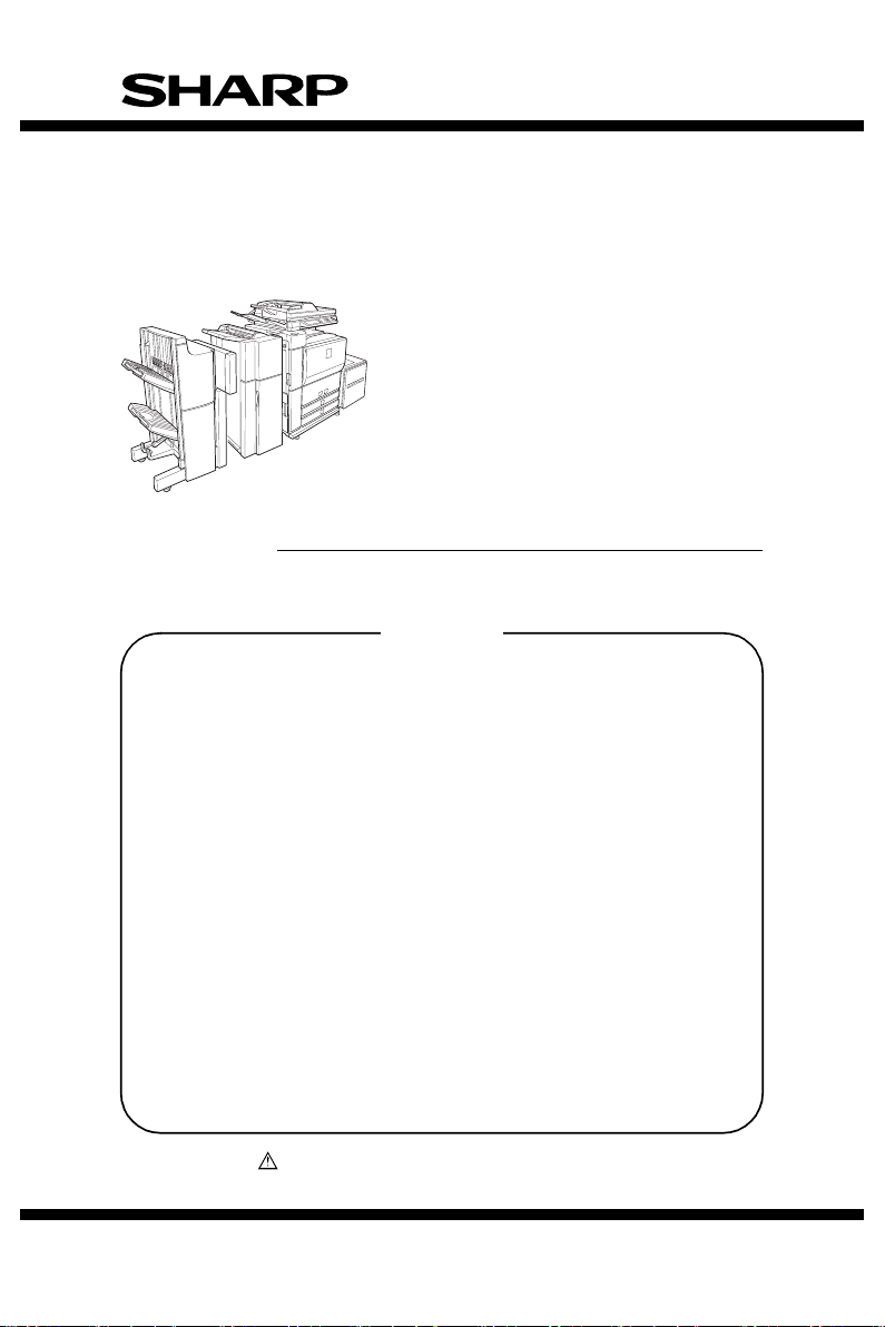
DIGITAL LASER COPIER/PRINTER
DIGITAL MULTIFUNCTIONAL SYSTEM
AR-M550N/M550U
AR-M620N/M620U
MODEL AR-M700N/M700U
CONTENTS
[1] CONSUMABLE PARTS . . . . . . . . . . . . . . . . . . . . . . . . . . 1-1
[2] STRUCTURE OF EACH SECTION . . . . . . . . . . . . . . . . . 2-1
[3] SETTING AND ADJUSTMENTS. . . . . . . . . . . . . . . . . . . . 3-1
[4] SIMULATION . . . . . . . . . . . . . . . . . . . . . . . . . . . . . . . . . . 4-1
[5] SELF DIAG MESSAGE AND TROUBLESHOOTING . . . .5-1
[6] ROM VERSION-UP METHOD . . . . . . . . . . . . . . . . . . . . . 6-1
[7] MAINTENANCE LIST . . . . . . . . . . . . . . . . . . . . . . . . . . . . 7-1
[8] OTHER . . . . . . . . . . . . . . . . . . . . . . . . . . . . . . . . . . . . . . . 8-1
[9] SIGNAL NAME LIST . . . . . . . . . . . . . . . . . . . . . . . . . . . . . 9-1
Parts marked with “ ” are important for maintaining the safety of the set. Be sure to replace
these parts with specified ones for maintaining the safety and performance of the set.
SHARP CORPORATION
This document has been published to be used
for after sales service only.
The contents are subject to change without notice.
Page 2
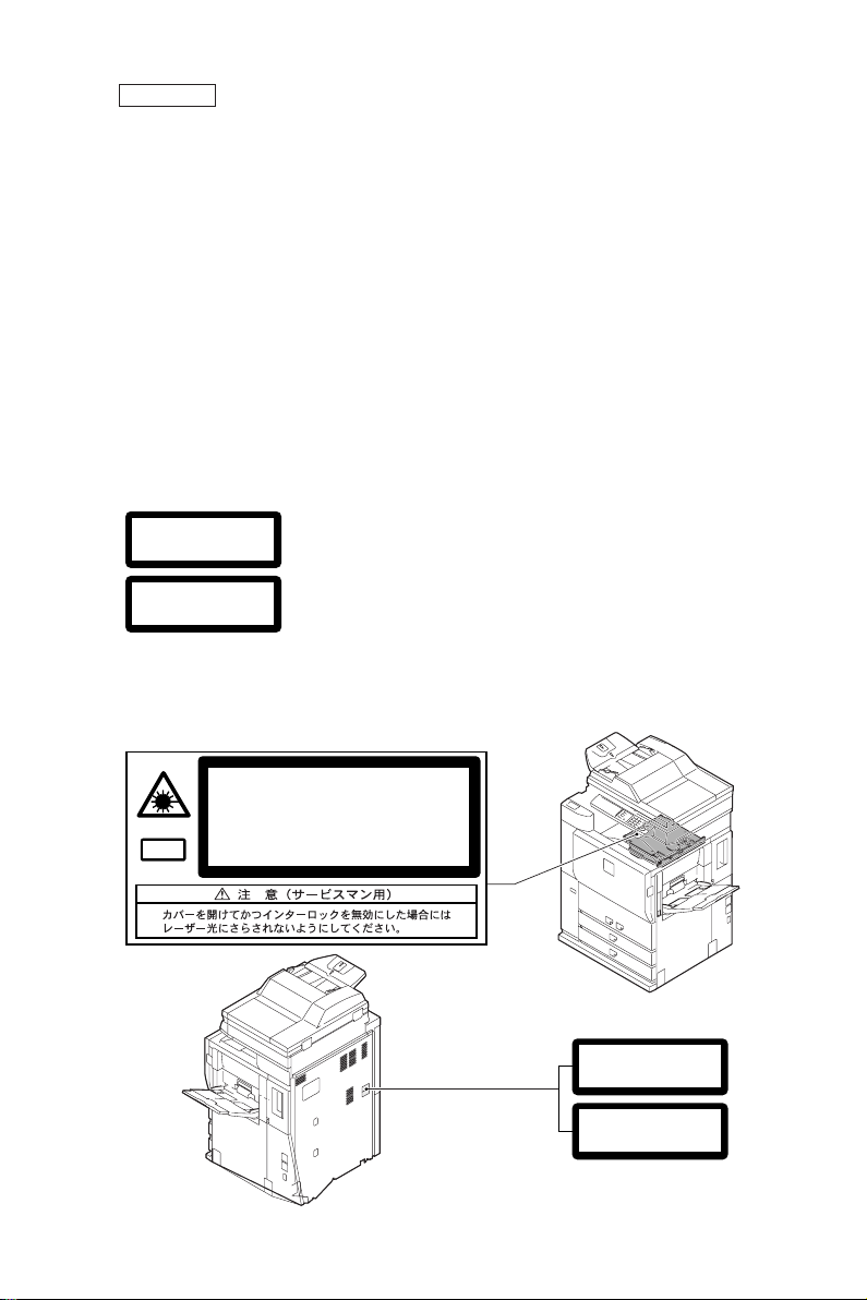
CAUTION
This product is a class 1 laser product that complies with 21CFR 1040 of the CDRH
standard and IEC825. This means that this machine does not produce hazardous laser
radiation. The use of controls, adjustments or performance of procedures other than
those specified herein may result in hazardous radiation exposure.
This laser radiation is not a danger to the skin, but when an exact focusing of the
laser beam is achieved on the eye’s retina, there is the danger of spot damage to the
The following cautions must be observed to avoid exposure of the laser beam to your
eyes at the time of servicing.
When a problem in the laser optical unit has occurred, the whole optical unit must
1)
be exchanged as a unit, not as individual parts.
Do not look into the machine with the main switch turned on after removing the
2)
developer unit, toner cartridge, and drum cartridge.
Do not look into the laser beam exposure slit of the laser optical unit with the
3)
connector connected when removing and installing the optical system.
The middle frame contains the safety interlock switch.
4)
Do not defeat the safety interlock by inserting wedges or other items into the
switch slot.
CLASS 1
LASER PRODUCT
LASER KLASSE 1
Wave length: 785 nm
Pulse times
North America: 55 cpm model (3.1 µs
Europe: 55 cpm model (3.7 µs
Output power: Max 0.8 mW
Laserstrahl
+10 nm
–15 nm
62 cpm model (3.1 µs
70 cpm model (2.7 µs
62 cpm model (3.7 µs
70 cpm model (3.2 µs
CAUTION
VORSICHT
ADVARSEL
ADVERSEL
VARNING
VAR O!
INVISIBLE LASER RADIATION,
WHEN OPEN AND INTERLOCKS DEFEATED.
AVOID EXPOSURE TO BEAM.
UNSICHTBARE LASERSTRAHLUNG,
WENN ABDECKUNG GEÖFFNET UND
SICHERHEITSVERRIEGELUNG ÜBERBRÜCKT.
NICHT DEM STRAHL AUSSETZEN.
± 3.1 ns)/7 mm
± 3.1 ns)/7 mm
± 2.7 ns)/7 mm
± 3.7 ns)/7 mm
± 3.7 ns)/7 mm
± 3.2 ns)/7 mm
INVISIBLE LASER RADIATION WHEN OPEN AND INTERLOCKS DEFEATED.
AVOID EXPOSURE TO BEAM.
UNSICHTBARE LASERSTRAHLUNG WENN ABDECKUNG GEÖFFNET UND
SICHERHEITSVERRIEGELUNG ÜBERERÜCKT. NICHT DEM STRAHL AUSSETZEN.
USYNLIG LASERSTRÅLING VED ÅBNING, NÅR SIKKERHEDSAFBRYDERE ER
UDE AF FUNKTION. UNDGÅ UDSAETTELSE FOR STRÅLNING.
USYNLIG LASERSTRÅLING NÅR DEKSEL ÅPNES OG SIKKERHEDSLÅS BRYTES.
UNNGÅ EKSPONERING FOR STRÅLEN.
OSYNLIG LASERSTRÅLNING NÄR DENNA DEL ÄR ÖPPNAD OCH SPÄRRAR ÄR
URKOPPLADE. STRÅLEN ÄR FARLIG. BETRAKTA EJ STRÅLEN.
AVATTAESSA JA SUOJALUKITUS OHITETTAESSA OLET ALTTIINA NÄKYMÄTÖNTÄ
LASERSÄTEILYLLE. ÄLÄ KATSO SÄTEESEEN.
CAUTION
VORSICHT
AVATTAESSA JA SUOJALUKITUS
OHITETTAESSA OLET ALTTIINA
NÄKYMÄTTÖMÄLLE LASERSÄTEILYLLE ÄLÄ
KATSO SÄTEESEEN.
USYNLIG LASERSTRÅLNING VED ÅBNING, NÅR
SIKKERHEDSBRYDERE ER UDE AF
FUNKTION. UNDGÅ UDSAETTELSE FOR
STRÅLNING.
OSYNLIG LASERSTRÅLNING NÄR DENNA DEL
ÄR ÖPPNAD OCH SPÄRREN ÄR URKOPPLAD.
BETRAKTA EJ STRÅLEN. – STRÅLEN ÄR
FARLIG.
VARO !
ADVARSEL
VARNING !
CLASS 1
LASER PRODUCT
LASER KLASSE 1
Page 3

CONTENTS
[1] CONSUMABLE PARTS
1. Supply system table . . . . . . . . . . . . . . . . . . . . . . . . . . . . . . . . . . . . . 1-1
A. USA, Canada, South and Central America . . . . . . . . . . . . . . . . . 1-1
B. Europe affiliates (Including East Europe, Russia)/Australia/
New Zealand/UK) . . . . . . . . . . . . . . . . . . . . . . . . . . . . . . . . . . . . 1-2
C. Asia affiliates . . . . . . . . . . . . . . . . . . . . . . . . . . . . . . . . . . . . . . . . 1-2
D. Hong Kong. . . . . . . . . . . . . . . . . . . . . . . . . . . . . . . . . . . . . . . . . . 1-3
E. China (AR-M620N/M700N) . . . . . . . . . . . . . . . . . . . . . . . . . . . . . 1-3
F. Middle East/Philippine . . . . . . . . . . . . . . . . . . . . . . . . . . . . . . . . . 1-4
G. Taiwan . . . . . . . . . . . . . . . . . . . . . . . . . . . . . . . . . . . . . . . . . . . . . 1-4
2. Maintenance parts list . . . . . . . . . . . . . . . . . . . . . . . . . . . . . . . . . . . . 1-5
A. USA, Canada. . . . . . . . . . . . . . . . . . . . . . . . . . . . . . . . . . . . . . . . 1-5
B. Europe affiliates (Including East Europe, Russia) Australia/
New Zealand/UK . . . . . . . . . . . . . . . . . . . . . . . . . . . . . . . . . . . . . 1-7
C. Middle East/Asia/South and Central America . . . . . . . . . . . . . . 1-10
D. China. . . . . . . . . . . . . . . . . . . . . . . . . . . . . . . . . . . . . . . . . . . . . 1-12
E. Taiwan. . . . . . . . . . . . . . . . . . . . . . . . . . . . . . . . . . . . . . . . . . . . 1-14
[2] STRUCTURE OF EACH SECTION
1. Operation panel section . . . . . . . . . . . . . . . . . . . . . . . . . . . . . . . . . . 2-1
2. Paper feed, paper transport, duplex,
and paper exit reverse sections . . . . . . . . . . . . . . . . . . . . . . . . . . . . 2-4
[Paper feed section] . . . . . . . . . . . . . . . . . . . . . . . . . . . . . . . . . . . . . 2-5
(Manual paper feed section) . . . . . . . . . . . . . . . . . . . . . . . . . . . . . . . 2-6
(Paper feed tray sections 1 and 2) . . . . . . . . . . . . . . . . . . . . . . . . . . 2-8
(Paper feed trays 3 and 4) . . . . . . . . . . . . . . . . . . . . . . . . . . . . . . . 2-10
[Paper Transport Section] . . . . . . . . . . . . . . . . . . . . . . . . . . . . . . . . 2-12
(Vertical paper transport section 1) . . . . . . . . . . . . . . . . . . . . . . . . . 2-12
(Vertical paper transport section 2) . . . . . . . . . . . . . . . . . . . . . . . . . 2-14
(Horizontal transport section) . . . . . . . . . . . . . . . . . . . . . . . . . . . . . 2-16
[Paper exit and turning section] . . . . . . . . . . . . . . . . . . . . . . . . . . . 2-18
(Duplex section) . . . . . . . . . . . . . . . . . . . . . . . . . . . . . . . . . . . . . . . 2-20
3. Laser scan unit (LSU) . . . . . . . . . . . . . . . . . . . . . . . . . . . . . . . . . . . 2-22
Page 4

4. Image process section . . . . . . . . . . . . . . . . . . . . . . . . . . . . . . . . . . 2-24
[Developer tank section] . . . . . . . . . . . . . . . . . . . . . . . . . . . . . . . . . 2-26
[OPC drum section]. . . . . . . . . . . . . . . . . . . . . . . . . . . . . . . . . . . . . 2-28
[Transfer section] . . . . . . . . . . . . . . . . . . . . . . . . . . . . . . . . . . . . . . 2-30
[Main charger section]. . . . . . . . . . . . . . . . . . . . . . . . . . . . . . . . . . . 2-32
5. Scanner section . . . . . . . . . . . . . . . . . . . . . . . . . . . . . . . . . . . . . . . 2-33
6. Fusing section. . . . . . . . . . . . . . . . . . . . . . . . . . . . . . . . . . . . . . . . . 2-36
7. SPF section. . . . . . . . . . . . . . . . . . . . . . . . . . . . . . . . . . . . . . . . . . . 2-42
[Paper feed tray section] . . . . . . . . . . . . . . . . . . . . . . . . . . . . . . . . . 2-44
[Paper feed/transport section]. . . . . . . . . . . . . . . . . . . . . . . . . . . . . 2-46
[CIS section] . . . . . . . . . . . . . . . . . . . . . . . . . . . . . . . . . . . . . . . . . . 2-48
[Paper exit section] . . . . . . . . . . . . . . . . . . . . . . . . . . . . . . . . . . . . . 2-50
[3] SETTING AND ADJUSTMENTS
[ADJ 1] Adjusting high voltage values . . . . . . . . . . . . . . . . . . . . . . . . . . 3-4
[ADJ 2] Adjusting the developing unit. . . . . . . . . . . . . . . . . . . . . . . . . . 3-13
[ADJ 3] Adjusting image distortions . . . . . . . . . . . . . . . . . . . . . . . . . . . 3-18
[ADJ 4] Adjusting the SPF parallelism . . . . . . . . . . . . . . . . . . . . . . . . . 3-31
[ADJ 5] Adjusting the image focus . . . . . . . . . . . . . . . . . . . . . . . . . . . . 3-36
[ADJ 6] Adjusting the image magnification . . . . . . . . . . . . . . . . . . . . . . 3-41
[ADJ 7] Adjusting the image off-center . . . . . . . . . . . . . . . . . . . . . . . . . 3-54
[ADJ 8] Adjusting the image position, image loss, and void area . . . . . 3-64
[ADJ 9] Adjusting the copied image quality . . . . . . . . . . . . . . . . . . . . . 3-77
[ADJ 10] Adjusting the print quality in fax mode . . . . . . . . . . . . . . . . . . . 3-87
[ADJ 11] Adjusting the image quality in scan mode . . . . . . . . . . . . . . . . 3-94
[ADJ 12] Common image quality adjustments for all of copy, scan,
and fax modes . . . . . . . . . . . . . . . . . . . . . . . . . . . . . . . . . . . . . 3-99
[ADJ 13] Adjusting the fusing paper guide position . . . . . . . . . . . . . . . 3-103
[ADJ 14] Adjusting the paper size detection . . . . . . . . . . . . . . . . . . . . . 3-104
[ADJ 15] Adjusting the original size detection
(in original table mode) . . . . . . . . . . . . . . . . . . . . . . . . . . . . . 3-110
[ADJ 16] Adjusting the touch panel coordinates . . . . . . . . . . . . . . . . . . 3-112
[ADJ 17] Adjusting the supply voltage . . . . . . . . . . . . . . . . . . . . . . . . . 3-113
[4] SIMULATION
1. Adjustment value/Simulation and storage data. . . . . . . . . . . . . . . . . 4-1
A. Simulation adjustment value/ Set value data. . . . . . . . . . . . . . . . 4-1
B. Each storage data . . . . . . . . . . . . . . . . . . . . . . . . . . . . . . . . . . . . 4-1
2. Simulation list . . . . . . . . . . . . . . . . . . . . . . . . . . . . . . . . . . . . . . . . . 4-11
3. Details. . . . . . . . . . . . . . . . . . . . . . . . . . . . . . . . . . . . . . . . . . . . . . . 4-41
Page 5

[5] SELF DIAG MESSAGE AND TROUBLESHOOTING
[Error code] . . . . . . . . . . . . . . . . . . . . . . . . . . . . . . . . . . . . . . . . . . . . . . . . 5-1
1. Breakdown sequence . . . . . . . . . . . . . . . . . . . . . . . . . . . . . . . . . . . . 5-1
A. Breakdown mode process . . . . . . . . . . . . . . . . . . . . . . . . . . . . . . 5-1
2. Trouble kind . . . . . . . . . . . . . . . . . . . . . . . . . . . . . . . . . . . . . . . . . . . 5-4
3. Details. . . . . . . . . . . . . . . . . . . . . . . . . . . . . . . . . . . . . . . . . . . . . . . 5-11
[6] ROM VERSION-UP METHOD
1. General . . . . . . . . . . . . . . . . . . . . . . . . . . . . . . . . . . . . . . . . . . . . . . . 6-1
A. Version-up target ROM's . . . . . . . . . . . . . . . . . . . . . . . . . . . . . . . 6-1
B. ROM version-up is required in the following cases:. . . . . . . . . . . 6-6
2. Precautions. . . . . . . . . . . . . . . . . . . . . . . . . . . . . . . . . . . . . . . . . . . . 6-7
A. Relationship between each ROM and version-up . . . . . . . . . . . . 6-7
3. Necessary items for Flash ROM version-up . . . . . . . . . . . . . . . . . . . 6-7
4. Flash ROM version-up method . . . . . . . . . . . . . . . . . . . . . . . . . . . . . 6-8
A. MFP control PWB ROM DIP switch selection and
Flash ROM slot . . . . . . . . . . . . . . . . . . . . . . . . . . . . . . . . . . . . . . 6-8
B. Operation panel . . . . . . . . . . . . . . . . . . . . . . . . . . . . . . . . . . . . . . 6-8
C. Version-up procedure 1 . . . . . . . . . . . . . . . . . . . . . . . . . . . . . . . . 6-9
D. Version-up procedure 2 . . . . . . . . . . . . . . . . . . . . . . . . . . . . . . . 6-11
E. Countermeasures against "Result: NG" . . . . . . . . . . . . . . . . . . 6-14
5. Turning OFF the power during the version-up procedure. . . . . . . . 6-14
[7] MAINTENANCE LIST
1. Maintenance list . . . . . . . . . . . . . . . . . . . . . . . . . . . . . . . . . . . . . . . . 7-1
2. Details. . . . . . . . . . . . . . . . . . . . . . . . . . . . . . . . . . . . . . . . . . . . . . . 7-10
A. Drum peripheral section . . . . . . . . . . . . . . . . . . . . . . . . . . . . . . 7-10
B. Transfer section . . . . . . . . . . . . . . . . . . . . . . . . . . . . . . . . . . . . . 7-13
C. Developing section . . . . . . . . . . . . . . . . . . . . . . . . . . . . . . . . . . 7-14
D. Fusing section . . . . . . . . . . . . . . . . . . . . . . . . . . . . . . . . . . . . . . 7-16
E. Scanner section . . . . . . . . . . . . . . . . . . . . . . . . . . . . . . . . . . . . . 7-20
F. SPF section . . . . . . . . . . . . . . . . . . . . . . . . . . . . . . . . . . . . . . . . 7-22
G. Paper feed section. . . . . . . . . . . . . . . . . . . . . . . . . . . . . . . . . . . 7-24
H. Transport section/paper exit reverse section/duplex section. . . 7-26
I. Drive section . . . . . . . . . . . . . . . . . . . . . . . . . . . . . . . . . . . . . . . 7-28
J. Filters. . . . . . . . . . . . . . . . . . . . . . . . . . . . . . . . . . . . . . . . . . . . . 7-30
3. Maintenance and disassembly . . . . . . . . . . . . . . . . . . . . . . . . . . . . 7-31
A. Necessary execution items in maintenance and servicing . . . . 7-31
Page 6

[8] OTHER
1. VARIOUS COUNTERS SPECIFICATIONS . . . . . . . . . . . . . . . . . . . 8-1
A. Count specification . . . . . . . . . . . . . . . . . . . . . . . . . . . . . . . . . . . 8-1
B. Location and display of each counter data . . . . . . . . . . . . . . . . 8-12
2. Web setting service mode. . . . . . . . . . . . . . . . . . . . . . . . . . . . . . . . 8-17
A. Outline . . . . . . . . . . . . . . . . . . . . . . . . . . . . . . . . . . . . . . . . . . . . 8-17
B. Operating procedures . . . . . . . . . . . . . . . . . . . . . . . . . . . . . . . . 8-17
C. Details . . . . . . . . . . . . . . . . . . . . . . . . . . . . . . . . . . . . . . . . . . . . 8-18
3. Paper jam code. . . . . . . . . . . . . . . . . . . . . . . . . . . . . . . . . . . . . . . . 8-21
A. Paper jam judgment conditions . . . . . . . . . . . . . . . . . . . . . . . . . 8-21
B. Inserter (AR-CF2) paper jam judgment conditions . . . . . . . . . . 8-32
C. Finisher (AR-F15/F16) paper jam judgment conditions. . . . . . . 8-33
[9] SIGNAL NAME LIST
Page 7
6% document
MT = NT x 10
MD = ND x 10
AR-620MD 1 Used two bags.
55ppm: 250k
AR-620DR 10
55ppm: 250k
[1] CONSUMABLE PARTS
x 10 720k (72k x 10) AR-620MT 1 * Life setting by A4/LT
1 Toner cartridge (Black) Toner cartridge (Black)
1. Supply system table
No. Part name Content Life Model name Packing Remark
A. USA, Canada, South and Central America
AR-M550/M620/M700 CONSUMABLE PARTS 1 - 1
(Toner; Net weight 1430g)
With IC chip
x 10 830k (83k x 10) AR-621MT
Toner cartridge (Black)
(Toner; Net weight 1650g)
With IC chip
x 10 62/70ppm: 300k
2 Developer (Black) Developer (Black)
(Developer; Net weight 725g)
3 Drum OPC drum x 1 62/70ppm: 300k
Page 8
6% document
LT = T x 10
LD = DV x 10
6% document
CT = ST x 10
CD = SD x 10
x 10 720k (72k x 10) AR-620LT 1 * Life setting by A4/LT
(Toner; Net weight 1430g)
With IC chip
x 10 830k (83k x 10) AR-621LT
Toner cartridge (Black)
(Toner; Net weight 1650g)
With IC chip
AR-620LD 1 Used two bags.
55ppm: 250k
x 10 62/70ppm: 300k
(Developer; Net weight 725g)
AR-620DM 10
55ppm: 250k
x 10 720k (72k x 10) AR-620CT 1 * Life setting by A4/LT
(Toner; Net weight 1430g)
With IC chip
x 10 830k (83k x 10) AR-621CT
Toner cartridge (Black)
(Toner; Net weight 1650g)
With IC chip
AR-620CD 1 Used two bags.
55ppm: 250k
x 10 62/70ppm: 300k
(Developer; Net weight 725g)
AR-620DR 10
55ppm: 250k
B. Europe affiliates (Including East Europe, Russia)/Australia/New Zealand/UK)
1 Toner cartridge (Black) Toner cartridge (Black)
No. Part name Content Life Model name Packing Remark
AR-M550/M620/M700 CONSUMABLE PARTS 1 - 2
2 Developer (Black) Developer (Black)
3 Drum OPC drum x 1 62/70ppm: 300k
1 Toner cartridge (Black) Toner cartridge (Black)
No. Part name Content Life Model name Packing Remark
C. Asia affiliates
2 Developer (Black) Developer (Black)
3 Drum OPC drum x 1 62/70ppm: 300k
Page 9
LT 6% document
CT-C = ST-C x 10
CD-C = SD-C x 10
AR-620CD-C 1 Used two bags.
55ppm: 250k
6% document
AR-620DR-C 10
55ppm: 250k
x 10 720k (72k x 10) AR-620CT-C 1 * Life setting by A4/
Toner cartridge (Black)
(Toner; Net weight 1430g)
With IC chip
For SRH
1 Toner cartridge (Black)
No. Part name Content Life Model name Packing Remark
D. Hong Kong
E. China (AR-M620N/M700N)
x 10 72k (72k x 1) AR-621ST-C 1 * Life setting by A4/LT
1 Toner cartridge (Black) Toner cartridge (Black)
No. Part name Content Life Model name Packing Remark
x 10 830k (83k x 10) AR-621CT-C
Toner cartridge (Black)
AR-M550/M620/M700 CONSUMABLE PARTS 1 - 3
(Toner; Net weight 1650g)
With IC chip
x 10 62/70ppm: 300k
(Developer; Net weight 725g)
2 Developer (Black) Developer (Black)
3 Drum OPC drum x 1 62/70ppm: 300k
(Toner; Net weight 1430g)
With IC chip
x 10 83k (83k x 1) AR-622ST-C
Toner cartridge (Black)
(Toner; Net weight 1650g)
x 10 62/70ppm: 300k AR-620SD-C 1 Used two bags.
With IC chip
(Developer; Net weight 725g)
2 Developer (Black) Developer (Black)
3 Drum OPC drum x 1 62/70ppm: 300k AR-620DR-C 1
Page 10
6% document
6% document
ET=FT x 10
CD = SD x 10
ET=FT x 10
LD = DV x 10
x 10 720k (72k x 10) AR-620ET 1 * Life setting by A4/LT
(Toner; Net weight 1430g)
With IC chip
x 10 830k (83k x 10) AR-621ET
Toner cartridge (Black)
(Toner; Net weight 1650g)
(Toner; Net weight 1650g)
With IC chip
AR-620LD 1 Used two bags.
55ppm: 250k
x 10 62/70ppm: 300k
(Developer; Net weight 725g)
AR-620DM 10
55ppm: 250k
AR-620CD 1 Used two bags.
AR-620DR 10
55ppm: 250k
55ppm: 250k
x 10 62/70ppm: 300k
With IC chip
(Developer; Net weight 725g)
x 10 720k (72k x 10) AR-620ET 1 * Life setting by A4/LT
(Toner; Net weight 1430g)
With IC chip
x 10 830k (83k x 10) AR-621ET
Toner cartridge (Black)
1 Toner cartridge (Black) Toner cartridge (Black)
No. Part name Content Life Model name Packing Remark
F. Middle East/Philippine
2 Developer (Black) Developer (Black)
3 Drum OPC drum x 1 62/70ppm: 300k
AR-M550/M620/M700 CONSUMABLE PARTS 1 - 4
1 Toner cartridge (Black) Toner cartridge (Black)
No. Part name Content Life Model name Packing Remark
G. Taiwan
3 Drum OPC drum x 1 62/70ppm: 300k
2 Developer (Black) Developer (Black)
Page 11
(AR-620BL) x 10
Model name Packing Remark
Life
55cpm 62cpm 70cpm
AR-620CB 1 AR-620CB =
300K
(x 10)
300K
(x 10)
(x 10)
Side seal R x 1
MC cleaning unit x 1
Cleaner blade x 1
Drum separation pawl x 4
Screen grid x 1
Toner reception seal x 1
Charging plate x 1
Paper dust removal unit x 1
DV seal x 1
DV side seal F x 1
DV side seal R x 1
Toner filter x 1
Transfer belt x 1
Transfer roller x 1
Transfer gear x 1
Fusing separation pawl (Upper) x 6
Fusing separation pawl (lower) x 2
2. Maintenance parts list
No. Name Content
A. USA, Canada
1 Maintenance kit 1 Side seal F x 1 250K 300K 300K AR-620KA 10
AR-M550/M620/M700 CONSUMABLE PARTS 1 - 5
2 Maintenance kit 2 Transfer cleaning roller x 1 250K 300K 300K AR-620KB 10
3 Upper heat reoller kit Upper heat roller x 1 250K 300K 300K AR-620UH 10
4 Lower heat roller kit Lower heat roller x 1 250K 300K 300K AR-620LH 10
5 Cleaner blade Cleaner blade x 10 250K
Page 12

(AR-620RC) x 10
(Common with the
cartridge for AR-F11/
F12)
(Common with the
cartridge for AR-F12)
Model name Packing Remark
Life
55cpm 62cpm 70cpm
– AR-620CR 1 AR-620CR =
300K
(x 10)
(x 10)
Cleaning sheet x 10 ––300K AR-700CR 1
Scraper unit x 10 250K
Sub heat roller cleaning unit x 10
Oil roller x 10
Cleaning roller bearing x 20
Pressure cleaning plate x 10
SF-SC11 20 Cartridge for AR-F15
5,000
times x 3
5,000
times x 3
times x 3
Heat roller bearing x 2
SPF take-up roller x 1
SPF reverse roller x 1
Main unit paper feed take-up roller x 1
Main unit paper feed reverse roller x 1
AR-SC3 40 Cartridge for AR-F16
2,000
2,000
times x 3
times x 3
times x 3
No. Name Content
6 Cleaning roller kit
(70cpm model)
(55/62cpm model)
8 Heat roller kit Sub heat roller x 1 250K 300K 300K AR-620HR 10
7 Maintenance kit 3
AR-M550/M620/M700 CONSUMABLE PARTS 1 - 6
9 DSPF roller kit SPF paper feed roller x 1 100K 100K 100K AR-620DF 10
10 Paper feed roller kit Main unit paper feed roller x 1 100K 100K 100K AR-620RT 10
11 Staple cartridge Finisher staple x 3 5,000
12 Staple cartridge Saddle finisher staple x 3 2,000
Page 13

Packing Remark
Model
Life
name
55cpm 62cpm 70cpm
B. Europe affiliates (Including East Europe, Russia) Australia/New Zealand/UK
No. Part name Content
Side seal R x 1
MC cleaning unit x 1
Cleaner blade x 1
Drum separation pawl x 4
Screen grid x 1
Toner reception seal x 1
Charging plate x 1
Paper dust removal unit x 1
DV seal x 1
DV side seal F x 1
DV side seal R x 1
Toner filter x 1
1 Maintenance kit 1 Side seal F x 1 250K 300K 300K AR-620KA 10
AR-M550/M620/M700 CONSUMABLE PARTS 1 - 7
Transfer belt x 1
Transfer roller x 1
Transfer gear x 1
2 Maintenance kit 2 Transfer cleaning roller x 1 250K 300K 300K AR-620KB 10
Page 14

Packing Remark
Model
Life
name
55cpm 62cpm 70cpm
No. Part name Content
Upper heat roller x 1 250K 300K – AR-620KC 5
3 Maintenance kit 3
Lower heat roller x 1
Fusing separation pawl (Upper) x 6
Fusing separation pawl (lower) x 4
Scraper unit x 1
Sub heat roller cleaning unit x 1
Sub heat roller x 1
Heat roller bearing x 2
Upper heat roller x 1 ––300K AR-700KC 5
Lower heat roller x 1
Fusing separation pawl (Upper) x 6
Fusing separation pawl (lower) x 4
Cleaning sheet x 1
Oil roller x 1
(55/62cpm model)
AR-M550/M620/M700 CONSUMABLE PARTS 1 - 8
Maintenance kit 3
(70cpm model)
Cleaning roller bearing x 2
Pressure cleaning plate x 1
Sub heat roller x 1
Heat roller bearing x 2
SPF take-up roller x 1
SPF reverse roller x 1
Main unit paper feed take-up roller x 1
Main unit paper feed reverse roller x 1
4 DSPF roller kit SPF paper feed roller x 1 100K 100K 100K AR-620DF 10
5 Paper feed roller kit Main unit paper feed roller x 1 100K 100K 100K AR-620RT 10
Page 15

Packing Remark
Model
(Common with the
(Common with the
cartridge for AR-F11/
F12)
name
SF-SC11 20 Cartridge for AR-F15
cartridge for AR-F12)
AR-SC3 40 Cartridge for AR-F16
Life
5,000
5,000
55cpm 62cpm 70cpm
times x 3
times x 3
times x 3
2,000
2,000
times x 3
times x 3
times x 3
No. Part name Content
6 Staple cartridge Finisher staple x 3 5,000
7 Staple cartridge Saddle finisher staple x 3 2,000
AR-M550/M620/M700 CONSUMABLE PARTS 1 - 9
Page 16

Life
Model name Packing Remark
55cpm 62cpm 70cpm
Side seal R x 1
MC cleaning unit x 1
Cleaner blade x 1
Drum separation pawl x 4
Screen grid x 1
Toner reception seal x 1
Charging plate x 1
Paper dust removal unit x 1
DV seal x 1
DV side seal F x 1
DV side seal R x 1
Toner filter x 1
Transfer belt x 1
Transfer roller x 1
Transfer gear x 1
1 Maintenance kit 1 Side seal F x 1 250K 300K 300K AR-620KA 10
No. Part name Content
C. Middle East/Asia/South and Central America
AR-M550/M620/M700 CONSUMABLE PARTS 1 - 10
2 Maintenance kit 2 Transfer cleaning roller x 1 250K 300K 300K AR-620KB 10
Page 17

Model name Packing Remark
Life
55cpm 62cpm 70cpm
Upper heat roller x 1 250K 300K – AR-620KC 5
Lower heat roller x 1
Fusing separation pawl (Upper) x 6
Fusing separation pawl (lower) x 4
Scraper unit x 1
Sub heat roller cleaning unit x 1
Sub heat roller x 1
Heat roller bearing x 2
Upper heat roller x 1 ––300K AR-700KC 5
Lower heat roller x 1
Fusing separation pawl (Upper) x 6
Fusing separation pawl (lower) x 4
Cleaning sheet x 1
Oil roller x 1
Cleaning roller bearing x 2
Pressure cleaning plate x 1
Sub heat roller x 1
Heat roller bearing x 2
SPF take-up roller x 1
SPF reverse roller x 1
Main unit paper feed take-up roller x 1
Main unit paper feed reverse roller x 1
(55/62cpm model)
3 Maintenance kit 3
No. Part name Content
AR-M550/M620/M700 CONSUMABLE PARTS 1 - 11
Maintenance kit 3
(70cpm model)
4 DSPF roller kit SPF paper feed roller x 1 100K 100K 100K AR-620DF 10
5 Paper feed roller kit Main unit paper feed roller x 1 100K 100K 100K AR-620RT 10
Page 18
(Common with the
cartridge for AR-F11/
F12)
(Common with the
cartridge for AR-F12)
Model name Packing Remark
Life
SF-SC11 20 Cartridge for AR-F15
5,000
5,000
55cpm 62cpm 70cpm
times x 3
times x 3
times x 3
AR-SC3 40 Cartridge for AR-F16
2,000
2,000
times x 3
times x 3
times x 3
Model name Packing Packing
Life
62cpm 70cpm
Side seal R x 1
MC cleaning unit x 1
Cleaner blade x 1
Drum separation pawl x 4
Screen grid x 1
Toner reception seal x 1
Charging plate x 1
Paper dust removal unit x 1
DV seal x 1
DV side seal F x 1
DV side seal R x 1
Toner filter x 1
6 Staple cartridge Finisher staple x 3 5,000
No. Part name Content
7 Staple cartridge Saddle finisher staple x 3 2,000
AR-M550/M620/M700 CONSUMABLE PARTS 1 - 12
D. China
No. Part name Content
1 Maintenance kit 1 Side seal F x 1 300K 300K AR-620KA 10
Page 19

Model name Packing Packing
Life
62cpm 70cpm
Transfer belt x 1
Transfer roller x 1
Transfer gear x 1
Upper heat roller x 1 300K – AR-620KC 5
Lower heat roller x 1
Fusing separation pawl (Upper) x 6
Fusing separation pawl (lower) x 4
Scraper unit x 1
Sub heat roller cleaning unit x 1
Heat roller bearing x 2
Upper heat roller x 1 – 300K AR-700KC 5
Lower heat roller x 1
Fusing separation pawl (Upper) x 6
Fusing separation pawl (lower) x 4
Heat seal plate N assembly x 1
Oil roller x 1
Cleaning roller bearing x 2
Pressure cleaning plate x 1
Sub heat roller x 1
Heat roller bearing x 2
SPF take-up roller x 1
SPF reverse roller x 1
No. Part name Content
(55/62cpm model)
2 Maintenance kit 2 Transfer cleaning roller x 1 300K 300K AR-620KB 10
3 Maintenance kit 3
AR-M550/M620/M700 CONSUMABLE PARTS 1 - 13
Maintenance kit 3
(70cpm model)
4 DSPF roller kit SPF paper feed roller x 1 100K 100K AR-620DF 10
Page 20
(Common with the
cartridge for AR-F11/F12)
(Common with the
cartridge for AR-F12)
Model name Packing Packing
Life
62cpm 70cpm
Model name Packing Packing
Life
55cpm 62cpm 70cpm
Side seal R x 1
MC cleaning unit x 1
Cleaner blade x 1
Drum separation pawl x 4
Screen grid x 1
Toner reception seal x 1
Charging plate x 1
Paper dust removal unit x 1
DV seal x 1
DV side seal F x 1
DV side seal R x 1
Toner filter x 1
x 3
x 3
AR-SC3 40 Cartridge for AR-F16
x 3
2,000 times
x 3
SF-SC11 20 Cartridge for AR-F15
5,000 times
Main unit paper feed take-up roller x 1
Main unit paper feed reverse roller x 1
No. Part name Content
5 Paper feed roller kit Main unit paper feed roller x 1 100K 100K AR-620RT 10
6 Staple cartridge Finisher staple x 3 5,000 times
AR-M550/M620/M700 CONSUMABLE PARTS 1 - 14
7 Staple cartridge Saddle finisher staple x 3 2,000 times
E. Taiwan
No. Part name Content
1 Maintenance kit 1 Side seal F x 1 250K 300K 300K AR-620KA 10
Page 21

Model name Packing Packing
Life
55cpm 62cpm 70cpm
No. Part name Content
Transfer belt x 1
2 Maintenance kit 2 Transfer cleaning roller x 1 250K 300K 300K AR-620KB 10
Upper heat roller x 1 250K 300K – AR-620KC 5
Transfer roller x 1
Transfer gear x 1
Lower heat roller x 1
Fusing separation pawl (Upper) x 6
Fusing separation pawl (lower) x 4
Scraper unit x 1
Sub heat roller cleaning unit x 1
Heat roller bearing x 2
Upper heat roller x 1 ––300K AR-700KC 5
Lower heat roller x 1
Fusing separation pawl (Upper) x 6
Fusing separation pawl (lower) x 4
Cleaning sheet x 1
Oil roller x 1
(55/62cpm model)
Maintenance kit 3
(70cpm model)
3 Maintenance kit 3
AR-M550/M620/M700 CONSUMABLE PARTS 1 - 15
Cleaning roller bearing x 2
Pressure cleaning plate x 1
Sub heat roller x 1
Heat roller bearing x 2
SPF take-up roller x 1
SPF reverse roller x 1
4 DSPF roller kit SPF paper feed roller x 1 100K 100K 100K AR-620DF 10
Page 22

(Common with the
cartridge for AR-
F11/F12)
(Common with the
cartridge for AR-
F12)
Model name Packing Packing
Life
55cpm 62cpm 70cpm
Main unit paper feed take-up roller x 1
Main unit paper feed reverse roller x 1
SF-SC11 20 Cartridge for AR-F15
5,000
5,000
times x 3
times x 3
times x 3
AR-SC3 40 Cartridge for AR-F16
2,000
2,000
times x 3
times x 3
times x 3
No. Part name Content
5 Paper feed roller kit Main unit paper feed roller x 1 100K 100K 100K AR-620RT 10
6 Staple cartridge Finisher staple x 3 5,000
AR-M550/M620/M700 CONSUMABLE PARTS 1 - 16
7 Staple cartridge Saddle finisher staple x 3 2,000
Page 23

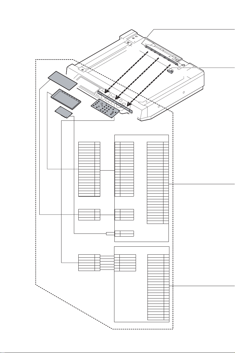
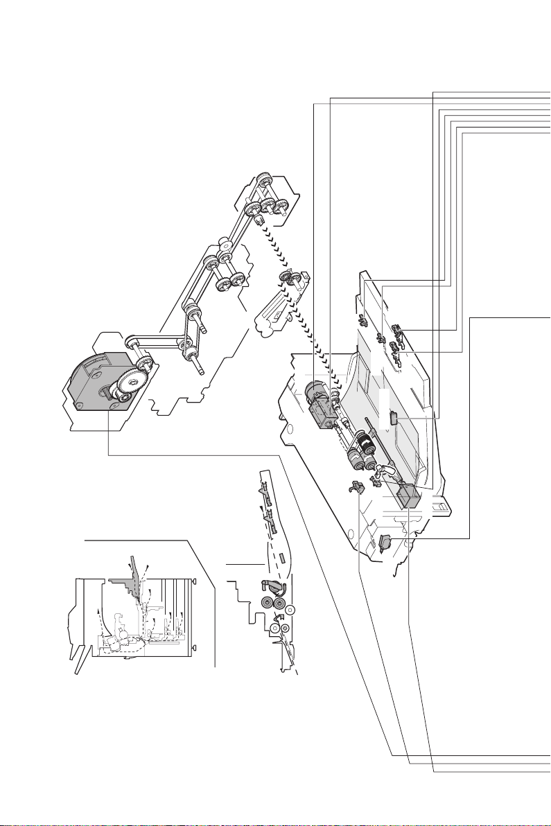
[2] STRUCTURE OF EACH SECTION
1. Operation panel section
A. General
This section describes various types of settings, display and operation.
The LCD display section is controlled by the MFP CONTROL PWB.
The touch panel, operation keys and LED display are controlled by the SCANNER
CONTROL PWB.
AR-M550/M620/M700 DETAILS OF EACH SECTION 2 - 1
Page 24
B. Major parts and signal functions
ORSLED
TOUCH
LCD
/CCFT
GND
N.C
N.C
N.C
N.C 16
GND
LCD D3
LCD D2
LCD D1
LCD D0
GND
LCD-VEE
3.3V3
lcd DIS
GND
CP2
GND
CP1
LCD M
LCD S
/YL
XH
YH
/XL
20
19
18
17
15
14
13
12
11
10
9
8
7
6
5
4
3
2
1
4
3
2
1
FFC-20Pin
FFC-4Pin
/ORSPD
CN4
20FLS-SM1-TB
1
GND
N.C
2
3
N.C
4
N.C
N.C
5
GND
6
7
LCD D3
LCD D2
8
9
LCD D1
10
LCD D0
GND
11
LCD-VEE
12
13
3.3V3
14
lcd DIS
GND
15
16
CP2
17
GND
18
CP1
19
LCD M
LCD S
20
CN2
04FM-1.0ST
/YL
1
XH
2
3
YH
/XL
4
CN3
S02(8.0)B-BHS-L
1
/CCFT
HV
2
CN1
30FMZ-BT
XH
/YL
/XL
YH
/CCFT
24V3
GND
TH
GND
lcdD3lcdD3+
lcdD2lcdD2+
lcdD1lcdD1+
lcdD0lcdD0+
LCD-VEE
3.3V3
lcdDIS
GND
lcdCP2lcdCP2+
GND
lcdCP1lcdCP1+
lcdMlcdM+
lcdSlcdS+
INVERTER
-LVDS PWB
OCSW
30
29
28
27
26
25
24
23
22
21
20
19
18
17
16
FFC-30Pin
15
14
13
12
11
10
9
8
7
6
5
4
3
2
1
PDSEL0
PDSEL1
PDSEL2
5V2
PD
GND
OPERATION PANEL
UNIT
AR-M550/M620/M700 DETAILS OF EACH SECTION 2 - 2
B6B-PH-K-S
CN102
1
2
3
4
5
6
B6B-PH-SM3-TB
1
PDSEL0
2
PDSEL1
PDSEL2
3
4
5V2
5
PD
GND
6
MFP
OPE
PWB
CN101
T24FAZ-SMT-TF
GND
5V1
/BZR
N.C
N.C
GND
GND
GND
/F3
/F2
/F1
/F0
SEG2
SEG1
SEG0
/KEYIN
5V2
GND
PD
5V2
PDSEL2
PDSEL1
PDSEL0
GND
1
2
3
4
5
6
7
8
9
10
11
FFC-24Pin
12
13
14
15
16
17
18
19
20
21
22
23
24
Page 25
SCN JNT
PWB
CN6
30FMZ-BT
XH
1
2
/YL
3
/XL
4
YH
/CCFT
5
24V3
6
7
GND
8
TH
9
GND
lcdD3-
10
11
lcdD3+
lcdD2-
12
lcdD2+
13
14
lcdD1-
15
lcdD1+
16
lcdD0-
17
lcdD0+
18
LCD-VEE
19
3.3V3
lcdDIS
20
GND
21
22
lcdCP2-
23
lcdCP2+
GND
24
25
lcdCP1-
26
lcdCP1+
lcdM-
27
28
lcdM+
29
lcdSlcdS+
30
CN5
T24FAZ-SMT-TF
24
GND
23
5V1
22
/BZR
21
N.C
N.C
20
19
GND
18
GND
17
GND
16
/F3
15
/F2
/F1
14
13
/F0
SEG2
12
SEG1
11
10
SEG0
/KEYIN
9
5V2
8
7
GND
PD
6
5
5V2
4
PDSEL2
PDSEL1
3
2
PDSEL0
GND
1
CN4
TX25-100P-LT-H1
GND
GND
/1_DBL/1_DBL+
1_CLK1_CLK+
1_DATA01_DATA0+
1_DATA11_DATA1+
1_DATA21_DATA2+
1_DATA31_DATA3+
GND
GND
/CCDFAN
12V2
24V3
24V3
PDSEL1
PDSEL2
/KEYIN
SEG0
GND
GND
lcdS+
lcdSlcdM+
lcdMlcdCP1+
lcdCP1lcdCP2+
lcdCP2lcdD0+
lcdD0lcdD1+
lcdD1lcdD2+
lcdD2lcdD3+
lcdD3GND
GND
YH
/XL
/STSET
/STMPS
GND
GND
GND
GND
12V2
12V2
GND
5V2
GND
5V2
GND
3.3V3
FRM_CCD1
CLK_CCD1
TXD_CCD1
RES_CCD1
RXD_CCD1
ADD_CCD1
GND
PAGE1
GND
GND
/CL1
PDSEL0
5V2
PD
SEG1
SEG2
GND
/F0
GND
/F1
GND
/F2
GND
/F3
GND
/BZR
GND
5V1
lcdDIS
3.3V3
GND
LCD_VEE
TH
/CCFT
/YL
XH
24V3
24V3
GND
GND
H3P-SHF-AA
+B3P-SHF-1AA
5V1
1
GND
2
OCSW
3
CN1
TX24-100R-LT-H1
1
100
2
3
4
5
6
7
8
9
10
11
12
13
14
15
16
17
18
19
20
21
22
23
24
25
26
27
28
29
30
31
32
33
34
35
36
37
38
39
40
41
42
43
44
45
46
47
48
49
50
51
52
53
54
55
56
57
58
59
60
61
62
63
64
65
66
67
68
69
70
71
72
73
74
75
76
77
78
79
80
81
82
83
84
85
86
87
88
89
90
91
92
93
94
95
96
97
98
99
GND
GND
/1_DBL/1_DBL+
1_CLK1_CLK+
1_DATA01_DATA0+
1_DATA11_DATA1+
1_DATA21_DATA2+
1_DATA31_DATA3+
GND
GND
/CCDFAN
12V2
24V3
24V3
PDSEL1
PDSEL2
/KEYIN
SEG0
GND
GND
lcdS+
lcdSlcdM+
lcdMlcdCP1+
lcdCP1lcdCP2+
lcdCP2lcdD0+
lcdD0lcdD1+
lcdD1lcdD2+
lcdD2lcdD3+
lcdD3GND
GND
YH
/XL
/STSET
/STMPS
GND
GND
GND
GND
12V2
12V2
GND
5V2
GND
5V2
GND
3.3V3
FRM_CCD1
CLK_CCD1
TXD_CCD1
RES_CCD1
RXD_CCD1
ADD_CCD1
GND
PAGE1
GND
GND
/CL1
PDSEL0
5V2
PD
SEG1
SEG2
GND
/F0
GND
/F1
GND
/F2
GND
/F3
GND
/BZR
GND
5V1
lcdDIS
3.3V3
GND
LCD_VEE
TH
/CCFT
/YL
XH
24V3
24V3
GND
GND
CN3
B6B-PH-K-S
5V1
GND
OCSW13
24V3 4
/LED0
/LED1
SCN
CONTROL
PWB
2
5
6
1
2
3
4
5
6
7
8
9
10
11
12
13
14
15
16
17
18
19
20
21
22
23
24
25
26
27
28
29
30
31
32
33
34
35
36
37
38
39
40
41
42
43
44
45
46
47
48
49
50
51
52
53
54
55
56
57
58
59
60
61
62
63
64
65
66
67
68
69
70
71
72
73
74
75
76
77
78
79
80
81
82
83
84
85
86
87
88
89
90
91
92
93
94
95
96
97
98
99
100
AR-M550/M620/M700 DETAILS OF EACH SECTION 2 - 3
Page 26
2. Paper feed, paper transport, duplex, and paper exit reverse sections
AR-M550/M620/M700 DETAILS OF EACH SECTION 2 - 4
Page 27

[Paper feed section]
General
The paper feed tray 1 holds 900 sheets, the paper feed tray 2 holds 1,300 sheets,
the multi-purpose paper feed tray 3 holds 500 sheets, the paper feed tray 4 holds
500 sheets, and the manual paper feed tray holds 100 sheets. Those paper feed
units are standard provisions.
AR-M550/M620/M700 DETAILS OF EACH SECTION 2 - 5
Page 28
(Manual paper feed section)
A. Major parts and signal functions
MM
MPFC
MTOP2
MTOP1
MPFPWS
MPLD2
MPLD1
MFPUS
MPFD1
MPED
DSW-R
AR-M550/M620/M700 DETAILS OF EACH SECTION 2 - 6
MPFGS
Page 29
GND2
GND2
+5V2
+5V2
MPLD1
MPLD2
DF3-3S-2C
DF3-3S-2C
2
1
8
9
GND2
MPLD1
PHNR-09-H+BU09P-TR-P-H
3
65432
7
MPLD2
+5V2
MTOP1
MTOP2
321
GND2
MPFPWS
179228-2
1
Vref
987654321
MTOP1
GND2
212
MTOP2
179228-2
1
GND2
PHR-3
GND2
MPFPWS
1
2
Vref
3
2
113
+24V1
3
PHNR-03-H+BU03P-TR-P-H
2
1
(NC)
/MPFC
+24V1
/MFPUS
2
1
232
SMR-02V-N/SMP-02V-NC
GND2
MPED
DF3-3S-2C
1
+5V2
2
1
+24V1
/MPFGS
MPFD1
GND2
+5V-MPFD1
PHR-3
1
2
SMR-02V-N/SMP-02V-NC
321
MPLD1
+5V2
MPLD2
MTOP1
8765432
MTOP2
GND2
CN-13
9
MPFPWS
987654321
B26B-PHDSS-B
1
DSW-F(R)
GND2
DRAWER
QR/P4-24S-C(01)/QR/P4-24P-C(01)
PCU PWB
M2LUM
GND2
+24V1
/T1PFC
B30B-PHDSS-B
CN-17
1
2
10
Vref
/MPFC
1
DSW-F(R)
+24V1
+24V1
2
(NC)
+24V1
+24V1
(NC)
/M2PFC
/DSKPFC2
/MFPUS
GND2
GND2
+24V1
GND2
GND2
9876543
17161514131211
MPED
+5V2
16151413121110
76543
MPLD1
/MFPUS
TXD-FIN
+5V2
+24V1
/MPFGS
191817
9
8
+5V2
GND2
RXD-FIN
201918
21
GND2
+5V-MPFD1
20
21
MPLD2
MPED
/DTR-FIN
/MM
MMCLK
1413121110
15
MPFD1
(NC)
MTOP1
+5V2
/DSR-FIN
MM-T
54321
242322
DSW-R
242322
MTOP2
+24V1
TSW-LED
RES-FIN
MPFPWS
/MPFGS
TSW
(NC)
Vref
+5V-MPFD1
/MPFC
GND2
GND2
242322212019181716
MPFD1
+24V1
GND2
GND2
DSW-DSK
TANSET
+5V2
2526272829
242322212019181716151413121110
GND2
(NC)
25
(NC)
26
DSW-R
+5V2
30
GND2
+5V2
/MM
MMCLK
MM-T
S5B-PH-K-S
AR-M550/M620/M700 DETAILS OF EACH SECTION 2 - 7
Page 30
(Paper feed tray sections 1 and 2)
A. Major parts and signal functions
PCU PWB
CN-14
B24B-PHDSS-B
B30B-PHDSS-B
B30B-PHDSS-B
T1LUM
T2LUM
GND2
GND2
+24V1
+24V1
/T1PUS
/T2PUS
+5V2
+24V1
GND2
/DSKLS
T1LUD
GND2
T1PED
T1SPD
+5V2
+5V2
GND2
GND2
T2LUD
T2SPD
T2PED
+5V2
CN-17
M2LUM
+24V1
GND2
/T1PFC
+24V1
+24V1
/M2PFC
/DSKPFC2
GND2
GND2
TXD-FIN
+5V2
RXD-FIN
/MM
/DTR-FIN
MMCLK
/DSR-FIN
MM-T
RES-FIN
TSW-LED
(NC)
TSW
GND2
GND2
TANSET
GND2
+5V2
DSW-DSK
(NC)
+5V2
CN-12
+24V1
+24V1
/T2PFC
/HPLS
+24V1
DVCH1
/HPFC
DVCH2
+24V1
DVCH3
/PSBC
DVCH4
+5V2
+24V1
PPD
TCS
GND2
GND2
+5V-MPRD1
TSGOUT
GND2
GND2
MPRD1
+5V2
+5V-MPRD2
HUS-DV
GND2
GND2
MPRD2
TH-DV
1
2
3
4
5
6
7
8
9
10
11
12
13
14
15
16
17
18
19
20
21
22
23
24
1
2
3
4
5
6
7
8
9
10
11
12
13
14
15
16
17
18
19
20
21
22
23
24
25
26
27
28
29
30
1
2
3
4
5
6
7
8
9
10
11
12
13
14
15
16
17
18
19
20
21
22
23
24
25
26
27
28
29
30
PHNR-03-H+BU03P-TR-P-H
+24V1
(NC)
2
/T1PFC
1
S5B-PH-K-S
1
GND2
2
+5V2
3
/MM
4
MMCLK
5
MM-T
PHR-3
1
GND2
2
TANSET
3
+5V2
13
2
3
PHNR-03-H+BU03P-TR-P-H
SMR-04V-N/SMP-04V-NC
1
+5V2
2
GND2
3
T1LUD
4
T1PED
SMP-10V-NC/SMR-10V-N
1
1
+5V2
2
2
GND2
3
3
T2LUD
4
4
T2PED
5
5
GND2
6
6
T1SPD
7
7
+5V2
8
8
GND2
9
9
T2SPD
10
10
+5V2
32+24V1
1 3
(NC)
/T2PFC
1
2
SMR-02V-N/SMP-02V-NC
SMR-02V-N/SMP-02V-NC
1
2
3
4
PHR-2
1
T1LUM
GND2
2
1
+24V1
2
/T1PUS
PHR-2
1
T2LUM
2
GND2
1
+24V1
2
/T2PUS
S4B-PH-K-S
1
+5V2
2
GND2
3
T1LUD
4
T1PED
S4B-PH-K-S
1
+5V2
2
GND2
3
T2LUD
4
T2PED
PHR-3
1
GND2
2
T1SPD
3
+5V2
PHR-3
1
GND2
2
T2SPD
3
+5V2
1
2
1
2
AR-M550/M620/M700 DETAILS OF EACH SECTION 2 - 8
Page 31

T1S PWB
MM
T1PUS
T1PFC
T1LUM
TANSET
T1SPD
T2S PWB
AR-M550/M620/M700 DETAILS OF EACH SECTION 2 - 9
T2PFC
T2LUM
T2SPD
T2PUS
Page 32

(Paper feed trays 3 and 4)
A. Major parts and signal functions
MM
M1PFD
M2PFD
M1LUD
M1PED
M1PWS
M2LUD
M2PED
DSKPFC1
M1PUS
M2PUS
M1PFC
M1SPD
M2SPD
M1LUM
M2LUM
M2PFC
M1SS PWB
M2SS PWB
AR-M550/M620/M700 DETAILS OF EACH SECTION 2 - 10
Page 33

PHR-2
M2LUM
GND2
PHNR-02-H+BU02P-TR-P-H
+24V1
1
/M2PFC
2
S6B-PH-K-S
(NC)
GND2
M1SS1
M1SS2
M1SS3
M1SS4
GND2
M1SPD
+5V2
S6B-PH-K-S
(NC)
GND2
M2SS1
M2SS2
M2SS3
M2SS4
GND2
M2SPD
+5V2
SMP-02V-NC/SMR-02V-N
+24V1
1
2
/M2PUS
PHR-3
GND2
M2PED
+5V2
PHR-3(RED)
GND2
M2LUD
+5V2
PHR-3
+5V-M2PFD
GND2
M2PFD
1
2
1
2
3
2
4
1
5
6
7
8
9
10 10
SMR-10V-N/SMP-10V-NC
1
2
3
4
5
6
PHR-3
PHR-3
SMP-02V-NC/SMR-02V-N
1
2
1
2
3
1
2
3
1
2
3
SMP-18V-NC/SMR-18V-N
1
2
3
1
2
3
4
5
6
1
2
3
+24V1
1
1
2
2
/M1PUS
PHR-3
GND2
1
2
M1PED
+5V2
3
PHR-3(RED)
GND2
1
2
M1LUD
+5V2
3
PHR-3
1
+5V-M1PFD
GND2
2
3
M1PFD
SMR-11V-N/SMP-11V-NC
+24V1
1
/M2PUS
2
GND2
3
M2PED
4
+5V2
5
6
GND2
M2LUD
7
+5V2
8
9
+5V-M2PFD
GND2
101110
11
M2PFD
PHNR-02-H+BU02P-TR-P-H
+24V1
1
/M1PFC
M1LUM
GND2
PHNR-02-H+BU02P-TR-P-H
1
+24V1
2
/DSKPFC1
Soldering
Vref
GND2
M1PWS
M2LUM
GND2
+24V1
/M2PFC
GND2
TXD-FIN
RXD-FIN
/DTR-FIN
/DSR-FIN
RES-FIN
1
GND2
2
M1SS1
3
M1SS2
4
M1SS3
5
M1SS4
6
GND2
M1SPD
7
8
+5V2
9
(NC)
10
GND2
11
M2SS1
12
M2SS2
13
M2SS3
14
M2SS4
15
GND2
16
M2SPD
17
+5V2
(NC)
18
SMR-11V-N/SMP-11V-NC
1
2
3
4
5
6
7
8
9
111011
1
2
3
4
5
6
7
8
9
2
12
PHR-2
1
2
2
1
3
1
2
1
2
3
4
5
6
7
8
9
S5B-PH-K-S
GND2
+5V2
/MM
MMCLK
MM-T
1
2
3
4
5
6
7
8
9
10
11
12
13
14
15
16
17
18
+24V1
1
/M1PUS
2
GND2
3
M1PED
4
+5V2
5
GND2
6
M1LUD
7
+5V2
8
9
+5V-M1PFD
GND2
10
M1PFD
SMR-03V-N/SMP-03V-NC
Vref
11
GND2
22
M1PWS
3
3
CN-17
B30B-PHDSS-B
M2LUM
1
+24V1
2
GND2
3
/T1PFC
4
+24V1
5
+24V1
6
/M2PFC
7
/DSKPFC2
8
GND2
9
GND2
10
TXD-FIN
11
+5V2
12
RXD-FIN
13
/MM
14
/DTR-FIN
15
MMCLK
16
/DSR-FIN
17
MM-T
18
RES-FIN
19
TSW-LED
20
(NC)
21
TSW
22
GND2
1
2
3
4
5
23
GND2
24
TANSET
25
GND2
26
+5V2
27
DSW-DSK
28
(NC)
29
+5V2
30
CN-15
B34B-PHDSS-B
DSW-F
1
2
(NC)
3
GND2
4
GND2
5
/GBPWM
6
/MHVREM
7
MHV-T
/THV+PWM
8
THV+REM
9
/CHV-PWM
10
/CHV-REM
11
12
/CHVACPWM
13
/CHVACREM
14
/DVPWM
15
/DVREM
16
HVREM
17
+24V1
18
(NC)
19
GND2
20
GND2
21
M1SS1
22
M2SS1
23
M1SS2
24
M2SS2
M1SS3
25
26
M2SS3
27
M1SS4
28
M2SS4
29
GND2
30
GND2
31
M1SPD
32
M2SPD
+5V2
33
+5V2
34
CN-16
B32B-PHDSS-B
+24V1
1
+24V1
2
/M1PUS
3
/M2PUS
4
GND2
5
GND2
6
M1PED
7
M2PED
8
+5V2
9
+5V2
10
GND2
11
12
GND2
M1LUD
13
M2LUD
14
+5V2
15
+5V2
16
+5V-M1PFD
17
18
+5V-M2PFD
19
GND2
20
GND2
21
M1PFD
22
M2PFD
23
+24V1
24
+24V1
/M1PFC
25
/DSKPFC1
26
27
M1LUM
Vref
28
GND2
29
GND2
30
(NC)
31
32
M1PWS
PCU PWB
AR-M550/M620/M700 DETAILS OF EACH SECTION 2 - 11
Page 34

[Paper Transport Section]
Outline
The paper transport section serves the function of transferring paper from each
paper feed port to the registration roller section.
Paper from manual feed, paper feed tray units 1 and 2 (optional), and the right
paper feed tray of the paper feed tray units 1 and 2 is transported horizontally,
whereas paper from the left paper feed tray of the paper feed tray units 1 and 2,
paper feed tray 3 and paper feed tray 4 is transported vertically to the registration
roller section.
After the leading edge of the paper is synchronized with the leading edge of the
drum image in the registration roller section, the paper that is transfer printed with
the image in the transfer section passes through the fusing section and is discharged either face-down or face-up.
(Vertical paper transport section 1)
A. Major parts and signal functions
MM
DSKPFC2
VPM
PHNR-02-H+BU02P-TR-P-H
1
S5B-PH-K-S
AR-M550/M620/M700 DETAILS OF EACH SECTION 2 - 12
+24V1
/DSKPFC2
GND2
+5V2
/MM
MMCLK
MM-T
2
12
1
2
3
4
5
Page 35

CN-17
B30B-PHDSS-B
M2LUM
1
+24V1
2
GND2
3
/T1PFC
4
+24V1
5
+24V1
6
7
/M2PFC
8
/DSKPFC2
9
GND2
10
GND2
11
TXD-FIN
12
+5V2
13
RXD-FIN
/MM
14
/DTR-FIN
15
MMCLK
16
/DSR-FIN
17
18
MM-T
RES-FIN
19
TSW-LED
20
21
(NC)
22
TSW
23
GND2
24
GND2
25
TANSET
GND2
26
27
+5V2
DSW-DSK
28
(NC)
29
+5V2
30
PCU PWB
CN-10
B26B-PHDSS-B
/POM1A
/POM1XA
/POM1B
/POM1XB
/POM2A
/POM2XA
/POM2B
/POM2XB
/ADM1A
/ADM1XA
/ADM1B
/ADM1XB
/ADM2A
/ADM2XA
/ADM2B
/ADM2XB
/TRMA
/TRMXA
/TRMB
/TRMXB
/VPMA
/VPMXA
/VPMB
/VPMXB
GND2
GND2
10
11
12
13
14
15
16
17
18
19
20
21
22
23
24
25
26
1
2
3
4
5
6
7
8
9
CN-4
B26B-PHDSS-B
/POM1A
1
/POM1XA
2
/POM1B
3
/POM1XB
4
/POM2A
5
6
/POM2XA
/POM2B
7
/POM2XB
8
/ADM1A
9
/ADM1XA
10
/ADM1B
11
/ADM1XB
12
/ADM2A
13
/ADM2XA
14
/ADM2B
15
/ADM2XB
16
/TRMA
17
/TRMXA
18
/TRMB
19
/TRMXB
20
/VPMA
21
/VPMXA
22
/VPMB
23
/VPMXB
24
GND2
25
GND2
26
DRIVER
PWB
AR-M550/M620/M700 DETAILS OF EACH SECTION 2 - 13
CN-2
B12B-PH-K-S
/TRM/A
/TRMA
/TRMB
/TRM/B
+24V2
+24V2
/VPM/A
/VPMA
/VPMB
/VPM/B
+24V2
+24V2
1
2
3
4
5
SMR-06V-N/SMP-06V-NC
6
7
1
/VPM/A
8
/VPMA
2
9
/VPMB
3
10
4
/VPM/B
11
5
+24V2
12
+24V2
6
1
2
3
4
5
6
Page 36

(Vertical paper transport section 2)
A. Major parts and signal functions
PSBC
MM
RRC
TRM
S5B-PH-K-S
1
GND2
2
+5V2
3
/MM
4
MMCLK
5
MM-T
PHNR-02-H+BU02P-TR-P-H
+24V1
1
2
2
1
/RRC
CN-17
B30B-PHDSS-B
M2LUM
1
+24V1
2
GND2
3
/T1PFC
4
+24V1
5
+24V1
6
/M2PFC
7
/DSKPFC2
8
GND2
9
GND2
10
TXD-FIN
11
+5V2
12
RXD-FIN
13
/MM
14
/DTR-FIN
15
MMCLK
16
/DSR-FIN
17
MM-T
18
RES-FIN
19
TSW-LED
20
(NC)
21
TSW
22
23
GND2
GND2
24
TANSET
25
GND2
26
+5V2
27
DSW-DSK
28
(NC)
29
+5V2
30
CN-7
B32B-PHDSS-B
1
+24V1
2
+24V1
3
/CFM-DV
4
/RRC
5
GND2
6
(NC)
7
+24V1
8
+24V(DSW)
9
+5V-APPD1
PFD2
10
11
+5V-APPD2
/CFM-ADU
12
+5V-PFD2
13
14
THPS2
15
+5V-DSWD
16
TURM
+5V-AINPD
17
/TCBPWH
18
19
+5V-THPS1
20
(NC)
21
+5V-THPS2
/TCBIAS
22
23
/FBIAS
APPD1
24
DSWD
25
APPD2
26
27
/DGS
AINPD
28
29
GND2
GND2
30
(NC)
31
32
DSW-L
PPD
MPRD2
PCU PWB
CN-12
B30B-PHDSS-B
+24V1
+24V1
/T2PFC
/HPLS
+24V1
DVCH1
/HPFC
DVCH2
+24V1
DVCH3
/PSBC
DVCH4
+5V2
+24V1
PPD
TCS
GND2
GND2
+5V-MPRD1
TSGOUT
GND2
GND2
MPRD1
+5V2
+5V-MPRD2
HUS-DV
GND2
GND2
MPRD2
TH-DV
CN-10
B26B-PHDSS-B
/POM1A
/POM1XA
/POM1B
/POM1XB
/POM2A
/POM2XA
/POM2B
/POM2XB
/ADM1A
/ADM1XA
/ADM1B
/ADM1XB
/ADM2A
/ADM2XA
/ADM2B
/ADM2XB
/TRMA
/TRMXA
/TRMB
/TRMXB
/VPMA
/VPMXA
/VPMB
/VPMXB
GND2
GND2
VPM
MPRD1
1
2
3
4
5
6
7
8
9
10
11
12
13
14
15
16
17
18
19
20
21
22
23
24
25
26
27
28
29
30
1
2
3
4
5
6
7
8
9
10
11
12
13
14
15
16
17
18
19
20
21
22
23
24
25
26
AR-M550/M620/M700 DETAILS OF EACH SECTION 2 - 14
Page 37

+24V1
1
1
2
/PSBC
2
+5V2
3
3
PPD
4
4
5
GND2
5
+5V-MPRD1
6
6
7
GND2
7
8
MPRD1
8
9
9
+5V-MPRD2
10
10
GND2
11
11
MPRD2
12
12
+24V1
13
13
/HPLS
14
14
(NC)
15
15
(NC)
16
16
(NC)
17
17
(NC)
18
18
(NC)
SMR-18V-N/SMP-18V-NC
PHNR-06-H+BU06P-TR-P-H
+24V1
1
6
/PSBC
2
5
+5V2
3
4
PPD
4
3
GND2
5
2
(NC)
61
SMR-08V-N/SMP-08V-NC
+5V-MPRD1
1
1
GND2
2
2
MPRD1
3
3
+5V-MPRD2
4
4
GND2
5
5
MPRD2
6
6
+24V1
7
7
8
8
/HPLS
PHNR-02-H+BU02P-TR-P-H
+24V1
1
2
12
/PSBC
179228-3
+5V2
1
PPD
2
3
GND2
PHR-3(RED)
1
+5V-MPRD1
2
GND2
3
MPRD1
PHR-3
+5V-MPRD2
1
GND2
2
3
MPRD2
CN-4
B26B-PHDSS-B
/POM1A
1
/POM1XA
2
/POM1B
3
/POM1XB
4
/POM2A
5
/POM2XA
6
/POM2B
7
/POM2XB
8
/ADM1A
9
/ADM1XA
10
/ADM1B
11
/ADM1XB
12
/ADM2A
13
/ADM2XA
14
/ADM2B
15
/ADM2XB
16
/TRMA
17
/TRMXA
18
/TRMB
19
/TRMXB
20
/VPMA
21
22
/VPMXA
/VPMB
23
/VPMXB
24
GND2
25
GND2
26
DRIVER PWB
CN-2
B12B-PH-K-S
/TRM/A
/TRMA
/TRMB
/TRM/B
+24V2
+24V2
/VPM/A
/VPMA
/VPMB
/VPM/B
+24V2
+24V2
1
2
3
4
5
6
7
8
9
10
11
12
AR-M550/M620/M700 DETAILS OF EACH SECTION 2 - 15
SMR-06V-N/SMP-06V-NC
/TRM/A
1
2
/TRMA
3
/TRMB
/TRM/B
4
5
+24V2
6
+24V2
SMR-06V-N/SMP-06V-NC
1
/VPM/A
2
/VPMA
3
/VPMB
4
/VPM/B
5
+24V2
6
+24V2
1
2
3
4
5
6
1
2
3
4
5
6
Page 38

(Horizontal transport section)
A. Major parts and signal functions
T1PPD
MPRD2
MPRD1
MPFD2
LPPD
HPFC
S5B-PH-K-S
GND2
+5V2
/MM
MMCLK
MM-T
1
2
3
4
5
MM
AR-M550/M620/M700 DETAILS OF EACH SECTION 2 - 16
Page 39

CN-17
B30B-PHDSS-B
M2LUM
1
+24V1
2
3
GND2
4
/T1PFC
+24V1
5
+24V1
6
/M2PFC
7
/DSKPFC2
8
GND2
9
GND2
10
TXD-FIN
11
+5V2
12
RXD-FIN
13
/MM
14
15
/DTR-FIN
16
MMCLK
17
/DSR-FIN
18
MM-T
19
RES-FIN
20
TSW-LED
21
(NC)
22
TSW
23
GND2
24
GND2
25
TANSET
GND2
26
27
+5V2
28
DSW-DSK
29
(NC)
30
+5V2
PCU PWB
CN-12
B30B-PHDSS-B
+24V1
+24V1
/T2PFC
/HPLS
+24V1
DVCH1
/HPFC
DVCH2
+24V1
DVCH3
/PSBC
DVCH4
+5V2
+24V1
PPD
TCS
GND2
GND2
+5V-MPRD1
TSGOUT
GND2
GND2
MPRD1
+5V2
+5V-MPRD2
HUS-DV
GND2
GND2
MPRD2
TH-DV
CN-18
B14B-PHDSS-B
GND2
+5V-MPFD2
TXD-LCC
GND2
RXD-LCC
MPFD2
/DTR-LCC
+5V-LPPD
/DSR-LCC
GND2
RES-LCC
LPPD
/TRC-LCC
(NC)
1
2
3
4
5
6
7
8
9
10
11
12
13
14
15
16
17
18
19
20
21
22
23
24
25
26
27
28
29
30
1
2
3
4
5
6
7
8
9
10
11
12
13
14
PHNR-02-H+BU02P-TR-P-H
2
+24V1
/HPFC
1
SMR-06V-N/SMP-06V-NC
+5V-MPFD2
1
2
3
4
5
6
GND2
MPFD2
+5V-LPPD
GND2
LPPD
1
2
3
4
5
6
1
2
SMP-06V-NC/SMR-06V-N
1
+5V-MPFD2
2
GND2
3
MPFD2
4
+5V-LPPD
5
GND2
6
LPPD
1
2
3
4
5
6
PHR-3
+5V-MPFD2
1
GND2
2
MPFD2
3
PHR-3
+5V-LPPD
1
GND2
2
LPPD
3
AR-M550/M620/M700 DETAILS OF EACH SECTION 2 - 17
Page 40

[Paper exit and turning section]
A. Outline
The paper exit and turning section discharges paper which is transported from the
fusing section, and detects paper full. It also turns paper to transport it to the
duplex or the finisher.
B. Major parts and signal functions
CN-1
B12B-PH-K-S
/POM1/A
1
/POM1A
2
/POM1B
3
/POM1/B
4
+24V2
5
+24V2
6
/POM2/A
7
/POM2A
8
/POM2B
9
/POM2/B
10
+24V2
11
+24V2
12
CN-5
DRIVER PWB
B26B-PHDSS-B
/POM1A
/POM1XA
/POM1B
/POM1XB
/POM2A
/POM2XA
/POM2B
/POM2XB
/ADM1A
/ADM1XA
/ADM1B
/ADM1XB
/ADM2A
/ADM2XA
/ADM2B
/ADM2XB
/TRMA
/TRMXA
/TRMB
/TRMXB
/VPMA
/VPMXA
/VPMB
/VPMXB
GND2
GND2
CN-4
PCU PWB
CN-10
1
2
3
4
5
6
7
8
9
10
11
12
13
14
15
16
17
18
19
20
21
22
23
24
25
26
B26B-PHDSS-B
/POM1A
1
/POM1XA
2
/POM1B
3
/POM1XB
4
/POM2A
5
/POM2XA
6
/POM2B
7
/POM2XB
8
/ADM1A
9
/ADM1XA
10
/ADM1B
11
/ADM1XB
12
/ADM2A
13
/ADM2XA
14
/ADM2B
15
/ADM2XB
16
/TRMA
17
/TRMXA
18
/TRMB
19
/TRMXB
20
/VPMA
21
/VPMXA
22
/VPMB
23
/VPMXB
24
GND2
25
GND2
26
B32B-PHDSS-B
GND2
+24V1
POD1
/VFM-EX1
+5V2
GND2
GND2
+24V1
POD2
/VFM-EX2
+5V2
GND2
GND2
+24V1
POD3
/VFM-EX3
+5V2
GND2
+24V1
+24V1
/CFM-U1
/VFM-BKL
GND2
GND2
+24V
+24V1
/CFM-U3
/CFM-U2
GND2
GND2
TH-EX
GND2
CN-8
B20B-PHDSS-B
/PWM-RSV1
1
2
3
4
5
6
7
8
9
10
11
12
13
14
15
16
17
18
19
20
21
22
23
24
25
26
27
28
29
30
31
32
20
AR-M550/M620/M700 DETAILS OF EACH SECTION 2 - 18
Page 41

POM1
INTPWB
CFM-U1
SMP-02V-NC/SMR-02V-N
/PWM-RSV1
11
2
(NS)
2
CFM-U3
CFM-U4
DELIVERY UNIT
SMP-18V-NC/SMR-18V-N
1
2
3
4
5
6
7
8
9
10
11
12
13
14
15
16
17
18
GND2
POD1
+5V2
GND2
POD2
+5V2
GND2
POD3
+5V2
+24V1
/CFM-U1
GND2
+24V1
/CFM-U3
GND2
TH-EX
GND2
/PWM-RSV1
1
2
3
4
5
6
7
8
9
10
11
12
13
14
15
16
17
18
POD1
POD2
POD3
SMR-06V-N/SMP-06V-NC
1
2
3
4
5
6
SMR-06V-N/SMP-06V-NC
1
2
3
4
5
6
1
2
3
1
2
3
1
2
3
SMR-03V-N/SMP-03V-NC
1
22
3
SMR-03V-N/SMP-03V-NC
1
22
3
PHNR-03-H+BU03P-TR-P-H
3
2
1
1
2
3
4
/POM1/A
/POM1A
/POM1B
/POM1/B
+24V2
+24V2
/POM2/A
/POM2A
/POM2B
/POM2/B
+24V2
+24V2
PHR-3
GND2
POD1
+5V2
PHR-3(RED)
GND2
POD2
+5V2
PHR-3
GND2
POD3
+5V2
+24V1
/CFM-U1
GND2
+24V1
/CFM-U3
GND2
+24V1
/PWM-RSV1
GND2
S4B-PH-K-S
(NC)
(NC)
TH-EX
GND2
POM2
1
2
3
4
5
6
1
2
3
4
5
6
1
3
1
3
1
2
3
AR-M550/M620/M700 DETAILS OF EACH SECTION 2 - 19
Page 42

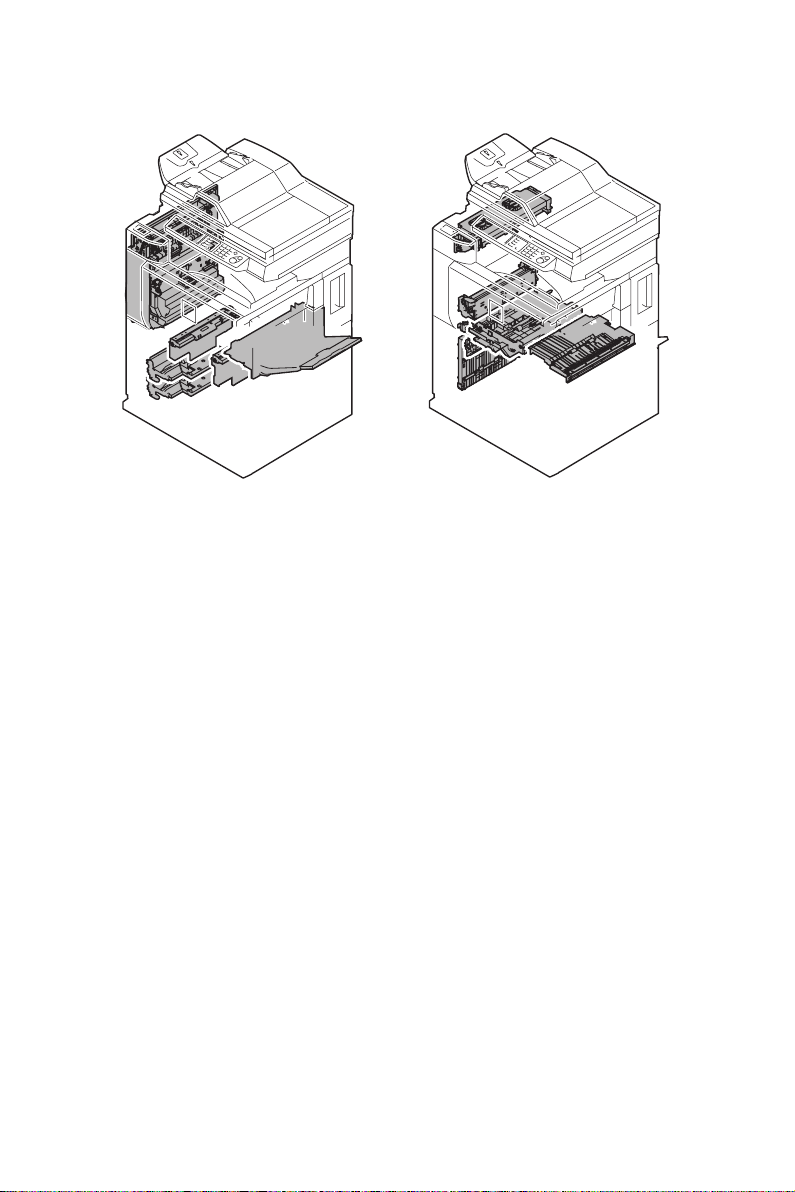
(Duplex section)
A. General
When duplex print is selected, paper one surface of which was printed is switched
back to feed to the duplex section to make duplex print.
B. Major parts and signal functions
DSW-L
ADM1
DSW-ADU
DGS
AINPD
ADM2
APPD1
TURM
APPD2
PFD2
THPS2
AR-M550/M620/M700 DETAILS OF EACH SECTION 2 - 20
Page 43

PHR-3
+5V-APPD1
GND2
APPD1
321
PHR-3
GND
+5V-APPD2
PHR-3
GND2
PFD2
APPD2
+5V-PFD2
321
321
1
+5V-PFD2
PFD2
+5V-THPS2
1
SMR-12V-N/SMP-12V-NC
179228-3
THPS2
/TCB-PWM
THPS2
/TCBIAS
GND2
+5V-THPS2
321
8765432
DSW-L
DSW-L
8765432
9
GND2
9
PHR-2
101112
TURM
101112
GND2
TURM
2
1
+24V1
/CFM-ADU
TB PWB
/TCBIAS
DSW-L
DSW-L
B6B-PH-K-S
Bias
FPS-187
/TCB-PWM
GND2
F-GND
54321
6
SRA-21T-4
1
+24V2
/ADUM2/A
/ADUM2A
/ADUM2B
/ADUM2/B
21345
SMR-06V-N/SMP-06V-NC
SRA-21T-4
65432
+24V2
6
SMR-06V-N/SMP-06V-NC
1
/ADUM1/A
/ADUM1A
/ADUM1B
21345
65432
+24V2
+24V2
/ADUM1/B
179228-3
6
PHNR-03-H+BU03P-TR-P-H
AINPD
1223
AINPD
3
+5V-AINPD
GND2
321
GND2
+5V-AINPD
1
DSW-ADU
179228-3
+5V-DSWD
GND2
321
2
12
+24V1
1 DGS
PHNR-02-H+BU02P-TR-P-H
987654321
DRAWER
/ADUM2/A
/ADUM2A
/ADUM2B
/ADUM2/B
/ADUM1/A
/ADUM1A
/ADUM1B
+5V-AINPD
+5V-PFD2
+5V-DSW
987654321
CN-7
B32B-PHDSS-B
(NC)
1
+24V1
2
+24V1
/RRC
/CFM-DV
/ADUM1/B
+24V(DSW)
+24V1
GND2
(NC)
+24V1
PFD2
+24V(DSW)
432
1
DSW-L
DSW-L
GND2
(NC)
/FBIAS
432
1
55
SMP-05V-NC/SMR-05V-N
DRIVER
CN-5
B9B-PH-K-S
PWB
/ADM1/A
/ADM1A
/ADM1B
/ADM1/B
/ADM2/A
/ADM2A
/ADM2/B
/ADM2B
987654321
+24V2
DSW-L
+5V-APPD1
+5V-APPD2
PCU PWB
AR-M550/M620/M700 DETAILS OF EACH SECTION 2 - 21
2019181716151413121110
21
TURM
THPS2
/CFM-ADU
2019181716151413121110
21
9876543
+5V-APPD1
+5V-APPD2
PFD2
242322
+5V-THPS2
/TCB-PWM
/TCBIAS
242322
+5V-PFD2
/CFM-ADU
THPS2
25262728293031
GND2
APPD1
APPD2
AINPD
GND2
25262728293031
+5V-DSWD
+5V-AINPD
+5V-THPS1
TURM
TCBWH
32
/DGS
+24V2
DSW-ADU
32
QR/P4-32S-C(01)/QR/P4-32P-C(01)
242322212019181716151413121110
25262728293031
+5V-THPS2
APPD1
APPD2
AINPD
/CFM-AM1
DSWD
/DGS
TCBIAS
(NC)
GND2
GND2
32
(NC)
DSW-L
LEFT DOOR UNIT
Page 44

3. Laser scan unit (LSU)
A. General
This section performs the following operations.
Image data sent from the MFP (image process circuit) through the mother board
and PCU are converted into laser beams to radiate onto the drum surface.
B. Major parts and signal functions
CN-8
MFP
CONTROL
PWB
CN-8
MOTHER
PWB
CN-6 CN-6
PCU PWB
B30B-PHDSS-B
GND2
+5VLD
GND2
GND2
/READY
/PMCLK
/START
+24V1
(NC)
+24V1
+5V2
GND2
+5V2
GND2
TEST
TEST2
VRB
GND2
TEST3
GND2
VIDEO
GND2
/VIDEO
GND2
LSU S/H
GND2
/LDON
GND2
/SYNC
GND2
CN-22
1
2
3
4
5
6
7
8
9
10
11
12
13
14
15
16
17
18
19
20
21
22
23
24
25
26
27
28
29
30
AR-M550/M620/M700 DETAILS OF EACH SECTION 2 - 22
Page 45

BD
PGM
CN-2
SMP-18V-NC/SMR-18V-N
1
2
3
4
5
6
7
8
9
10
11
12
13
14
15
16
17
18
1
2
3
4
5
6
7
8
9
10
11
12
SMP-12V-NC/SMR-12V-N
GND2
+5VLD
GND2
GND2
/READY
/PMCLK
/START
+24V1
(NC)
+24V1
+5V2
GND2
+5V2
GND2
TEST
TEST2
VRB
GND2
TEST3
GND2
/VIDEO
VIDEO
GND2
GND2
LSU S/H
GND2
/LDON
GND2
/SYNC
GND2
1
2
3
4
5
6
7
8
9
10
11
12
13
14
15
16
17
18
10
11
12
1
2
3
4
5
6
7
8
9
B30B-PHDSS-B
GND2
1
+5VLD
2
3
GND2
4
GND2
5
/READY
6
/PMCLK
/START
7
8
+24V1
9
/BRAKE
10
+24V1
11
+5V2
12
GND2
13
+5V2
14
GND2
TEST
15
TEST2
16
VRB
17
GND2
18
19
TEST3
GND2
20
/VIDEO
21
GND2
22
23
VIDEO
24
GND2
25
LSU S/H
26
GND2
27
/LDON
28
GND2
29
/SYNC
GND2
30
LD PWB
LSU UNIT
AR-M550/M620/M700 DETAILS OF EACH SECTION 2 - 23
CN-1
B6B-PH-K-S
/BRAKE
/PMCLK
/READY
/START
GND2
+24V1
CN-3
B4B-PH-K-S
GND2
/SYNC
GND2
+5V2
1
2
3
4
5
6
1
2
3
4
Page 46

4. Image process section
A. General
Toner is attached to electrostatic latent images formed by the laser beams which
were radiated to the OPC drum charged by the main charger, forming toner
images.
The toner images formed on the OPC drum are transferred to paper by the transfer belt.
B. Major parts and signal functions
TM1X
TFSD
CRUM
AR-M550/M620/M700 DETAILS OF EACH SECTION 2 - 24
TM2X
Page 47

PCU PWB
TM1a
TM1b
TM2a
CRUCLK
+5V2
GND2
B12B-PHDSS-B
CN-11
1
2
987654321
11
10
+24V1
TFSD
GND2
TM1a
TM1b
GND2
+5V2
CRUCLK
CRUSDA
(NC)
(NC)
TSDP-12V-K/TSDR-12V-K
432
1
PHR-4
TONER HOPPER
+24V1
TFSD
(NC)
GND2
987654321
11
10
1
TM1a
1
SMR-02V-N/SMP-02V-NC
GND2
+24V1
TM2b
TFSD
CRUSDA
76543
9
8
10
11
SRA-01T-3.2
12
GND2
12
SRA-01T-3.2
1
2
TM1b
GND2
2
DRAWER TSR-04V-K
TNCA
12
CRUCLK
+5V2
432
CRUSDA
1
TM2a
1
SMR-02V-N/SMP-02V-NC
2
TM2b
2
AR-M550/M620/M700 DETAILS OF EACH SECTION 2 - 25
Page 48

[Developer tank section]
A. General
In this section, toner is attached to electrostatic latent images formed by laser
beams on the OPC drum, making visible images.
B. Major parts and signal functions
DVM
HUS-DV
TH-DV
TCS
AR-M550/M620/M700 DETAILS OF EACH SECTION 2 - 26
Page 49

DEVELOPER UNIT
51021-0400
1
TSGOUT
2
+24V1
3
TCS
4
GND2
ZHR-4
1
+5V2
2
HUS-DV
3
GND2
4
TH-DV
SRA-01T-3.2
QR/P8-20S-C(01)/QR/P8-20P-C(01)
1
2
3
4
5
6
7
8
9
10
11
12
13
14
15
16
17
18
19
20
DRAWER
DVCH1
DVCH2
DVCH3
DVCH4
+24V1
TCS
GND2
TSGOUT
(NC)
GND2
(NC)
+5V2
HUS-DV
GND2
TH-DV
(NC)
(NC)
(NC)
(NC)
DV-Bias
B2PS-VH
+38V
GND1
S5B-PH-K-S
GND2
+5V2
/DVM
DVMCLK
DVM-T
1
2
3
4
5
6
7
8
9
10
11
12
13
14
15
16
17
18
19
20
CN-5
B16B-PADSS-1
+38V
10
+38V
11
+38V
12
GND1
14
GND1
15
GND1
16
1
2
1
2
3
4
5
CN-6
B18B-PHDSS-B
1
GND2
2
GND2
3
+5V2
4
+5V2
5
/DM
6
/DVM
7
DMCLK
8
DVMCLK
9
DM-T
10
DVM-T
11
GND2
12
+5V2
13
/FUM
14
FUMCLK
15
FUM-T
16
+24V1
17
/VFM-BKR
18
GND2
CN-12
B30B-PHDSS-B
1
+24V1
+24V1
2
/T2PFC
3
4
/HPLS
5
+24V1
DVCH1
6
7
/HPFC
DVCH2
8
+24V1
9
10
DVCH3
11
/PSBC
12
DVCH4
13
+5V2
14
+24V1
15
PPD
16
TCS
17
GND2
18
GND2
19
+5V-MPRD1
20
TSGOUT
21
GND2
22
GND2
MPRD1
23
+5V2
24
+5V-MPRD2
25
26
HUS-DV
27
GND2
28
GND2
29
MPRD2
TH-DV
30
PS-187(GR)
Bias
AC PWB
PCU PWB
CN-15
B34B-PHDSS-B
/DVPWM
/DVREM
HVREM
+24V1
DVREM
HV
CN1
14
15
16
17
AR-M550/M620/M700 DETAILS OF EACH SECTION 2 - 27
Page 50

[OPC drum section]
A. General
In this section, laser beams are radiated to the OPC drum surface which was negatively charged, making electrostatic latent images.
B. Major parts and signal functions
2
3212321
1
+38V
GND1
B2PS-VH
S5B-PH-K-S
2
1
10
CN-5
+38V
+38V
+38V
B16B-PADSS-1
PCS
+12V2
PCS-LED
1
3
SMR-03V-B/SMP-03V-BC
PROCESS UNIT
+5V2
GND2
/DVM
DVMCLK
DVM-T
54321
1615141211
CN-6
+5V2
GND2
GND1
GND1
GND1
GND2
B18B-PHDSS-B
DMS
+12V2
DMS-LED
+24V-DL
/DL
(NC)
PHR-3
2
1
332
SMR-03V-B/SMP-03V-BC
/DM
+5V2
1
DRAWER
PCS-LED
PCS
TSDR-20V-K/TSDP-20V-K
987654321
DM-T
/DVM
GND2
DVM-T
DMCLK
DVMCLK
+12V2
+5V2
/PSPS
(NC)
+24V1
S4B-PH-K-S
1
1
2
SMP-02V-BC/SMR-02V-B
987654321
DMS-LED
DMS
/DL
/PTDL
(NC)
+24V1
+12V2
+24V-DL
987654321
181716151413121110
+24V1
FUM-T
CN-8
GND2
/VFM-BKR
B20B-PHDSS-B
/FUM
FUMCLK
GND2
TH-CL
(NC)
432
/PSPS
TH-CL
+24V1
PCS-LED
DMS-LED
GND2
PCS
DMS
(NC)
+12V2
(NC)
+12V2
SRA-01T-3.2
(NC)
(NC)
+24V1
+24V-DL
2019181716151413121110
GND2
2019181716151413121110
SRA-01T-3.2
987654321
/DL
/PTDL
+24V1
TH-CL
GND2
/PSPS
+5V2
TLS
GND2
HUS-TC
2019181716151413121110
GND2
/PWM-RSV1
AC PWB
PCU PWB
AR-M550/M620/M700 DETAILS OF EACH SECTION 2 - 28
Page 51

PCS
DM
PSPS
TH-CL
DL
DMS
AR-M550/M620/M700 DETAILS OF EACH SECTION 2 - 29
Page 52

[Transfer section]
A. General
In this section, toner images on the OPC drum are transferred to paper.
B. Major parts and signal functions
DM
TURM
THPS2
HV
FPS-187(WH)
THV
CN-1
B16B-PH-K-S
MHV-T
/THV+PWM
THV+REM
/CHV-PWM
AR-M550/M620/M700 DETAILS OF EACH SECTION 2 - 30
6
7
8
9
Page 53

CN-15
B34B-PHDSS-B
MHV-T
7
8
/THV+PWM
9
THV+REM
/CHV-PWM
10
CN-8
B20B-PHDSS-B
1
PCS-LED
2
DMS-LED
3
PCS
4
DMS
+12V2
5
+12V2
6
+24V-DL
7
+24V1
8
9
/DL
10
/PTDL
+24V1
11
12
TH-CL
13
/PSPS
14
GND2
+5V2
15
16
TLS
17
HUS-TC
18
GND2
19
GND2
20
(NC)
PCU
PWB
CN-7
B32B-PHDSS-B
+24V1
+24V1
/CFM-DV
/RRC
GND2
(NC)
+24V1
+24V(DSW)
+5V-APPD1
PFD2
+5V-APPD2
THPS1
+5V-PFD2
THPS2
+5V-DSWD
TURM
+5V-AINPD
/SFM
+5V-THPS1
(NC)
+5V-THPS2
(NC)
/CFM-AM1
APPD1
DSWD
APPD2
/DGS
AINPD
GND2
GND2
(NC)
DSW-L
B1v8B-PHDSS-B
GND2
GND2
+5V2
+5V2
/DM
/DVM
DMCLK
DVMCLK
DM-T
DVM-T
GND2
+5V2
/FUM
FUMCLK
FUM-T
+24V1
/VFM-BKR
GND2
1
2
3
4
5
6
7
8
9
10
11
12
13
14
15
16
17
18
19
20
21
22
23
24
25
26
27
28
29
30
31
32
QR/P4-32S-C(01)/QR/P4-32P-C(01)
AC PWB
CN-6
1
2
3
4
5
6
7
8
9
10
11
12
13
14
15
16
17
18
19
20
21
22
23
24
25
26
27
28
29
30
31
32
1
2
3
4
5
6
7
8
9
10
11
12
13
14
15
16
17
18
DRAWER
DSW-L
/ADUM2/A
/ADUM2A
/ADUM2B
/ADUM2/B
+5V-APPD1
+5V-APPD2
+5V-PFD2
+5V-DSW
+5V-AINPD
(NC)
/ADUM1/A
/ADUM1A
/ADUM1B
/ADUM1/B
+24V1
+24V(DSW)
PFD2
/CFM-ADU
THPS2
TURM
/TCB-PWM
/TCBIAS
+5V-THPS2
GND2
GND2
APPD1
APPD2
AINPD
DSW-ADU
/DGS
+24V2
1
2
3
4
5
LEFT DOOR UNIT
6
7
8
9
10
SMR-12V-N/SMP-12V-NC
11
+5V-PFD2
1
12
2
13
3
14
4
15
5
16
17
6
7
18
8
19
9
20
10
21
11
22
12
23
24
25
26
27
28
29
30
31
32
B16B-PADSS-1
+38V
+38V
+38V
GND1
GND1
GND1
PFD2
+5V-THPS2
THPS2
/TCB-PWM
/TCBIAS
DSW-L
DSW-L
GND2
TURM
+24V1
/CFM-ADU
CN-5
10
11
12
14
15
16
1
2
3
4
5
6
7
8
9
10
11
12
1
2
3
4
5
6
B6B-PH-K-S
DSW-L
DSW-L
/TCBIAS
/TCB-PWM
GND2
F-GND
179228-3
1
THPS2
2
GND2
3
+5V-THPS2
PHR-2
TURM
21GND2
FPS-187
TB PWB
S5B-PH-K-S
1
GND2
2
+5V2
3
/DM
4
DMCLK
5
DM-T
B2PS-VH
1
+38V
2
GND1
Bias
AR-M550/M620/M700 DETAILS OF EACH SECTION 2 - 31
Page 54

[Main charger section]
A. General
The OPC drum surface is negatively charged in this section.
B. Major parts and signal functions
CN-15
B34B-PHDSS-B
1
2
3
4
5
6
7
8
9
10
11
12
13
14
15
16
17
18
19
PS-187(RD)
MHV
PS-187(YL)
GB
FPS-187(WH)
THV
PS-187(GR)
Bias
HV
CN-1
B16B-PH-K-S
DSW-F
GND2
GND2
/GBPWM
/MHVREM
MHV-T
/THV+PWM
THV+REM
/CHV-PWM
/CHV-REM
/CHVACPWM
/CHVACREM
/DVPWM
/DVREM
HVREM
+24V1
1
2
3
4
5
6
7
8
9
10
11
12
13
14
15
16
PCU PWB
DSW-F
(NC)
GND2
GND2
/GBPWM
/MHVREM
MHV-T
/THV+PWM
THV+REM
/CHV-PWM
/CHV-REM
/CHVACPWM
/CHVACREM
/DVPWM
/DVREM
HVREM
+24V1
(NC)
GND2
AR-M550/M620/M700 DETAILS OF EACH SECTION 2 - 32
Page 55

5. Scanner section
A. General
There are following three methods of scanning documents in this machine.
a. Place a document on the table glass. The copy lamp unit is operated to radiate
copy lamp light onto the document, scanning the document with the CCD.
b. The SPF feeds a document. The copy lamp light is radiated onto the document
which is stopped at the specified position and the document is scanned by the
CCD.
c. The SPF feed a document. The LED light of the CIS unit which is attached to
the SPF is radiated to the back of the document, and the document is scanned
by the CIS.
AR-M550/M620/M700 DETAILS OF EACH SECTION 2 - 33
Page 56

B. Major parts and signal functions
CN3
CIScnt
PWB
CN1
B26B-PHDSS
2_DATA1-
1
2_DATA1+
2
2_DATA0-
3
2_DATA0+
4
2_CLK-
5
2_CLK+
6
/2_DBL-
7
/2_DBL+
8
GND
9
10
FRM_CCD2
CLK_CCD2
11
12
PAGE2
13
ADD_CCD2
TXD_CCD2
14
15
RES_CCD2
16
RXD_CCD2
3.3V3
17
3.3V3
18
24V3
19
20
GND
12V2
21
GND
22
5V2
23
GND
24
5V2
25
26
/CISSET
9604S-35F
SD7
GND
SD6
GND
SD5
GND
SD4
GND
SD3
GND
SD2
GND
SD1
GND
SD0
GND
/LST
GND
SCLK
GND
LD
GND
DATA
GND
CLK
GND
LGATE
GND
SCN
GND
VDS
GND
VAS
GND
VLED
1
2
3
4
5
6
7
8
9
10
11
12
13
14
15
FFC-35Pin
16
17
18
19
20
21
22
23
24
25
26
27
28
29
30
31
32
33
34
35
MHPS
CIS unit
CIS unit
Copy lamp unit
CL
MHPS
CL1
Scanner motor
CCD PWB
CCD lens unit
Copy lamp unit
MIMDA
CCD PWB
SLD5R-1 (FCI)
GND
GND
/CL1
24V3
24V3
AR-M550/M620/M700 DETAILS OF EACH SECTION 2 - 34
1
2
3
4
5
Page 57

FFC-40Pin
FFC-5Pin
SCN
JNT
PWB
CN2
IL-FPR-40S-VF-E1500
GND
40
1_DATA3+
39
1_DATA3-
38
1_DATA2+
37
36
1_DATA2-
35
1_DATA1+
1_DATA1-
34
1_DATA0+
33
32
1_DATA0GND
31
1_CLK+
30
1_CLK-
29
GND
28
/1_DBL+
27
/1_DBL-
26
GND
25
FRM_CCD1
24
/PAGE1
23
CLK_CCD1
22
ADD_CCD1
21
TXD_CCD1
20
RXD_CCD1
19
RES_CCD1
18
GND
17
3.3V3
16
3.3V3
15
GND
14
5V2
13
5V2
12
5V2
11
10
5V2
9
5V2
8
5V2
7
5V2
6
5V2
GND
5
12V2
4
3
12V2
2
GND
GND
1
CN3
SLD5R-1 (FCI)
1
GND
GND
2
3
/CL1
4
24V3
5
24V3
CN4
TX25-100P-LT-H1
GND
GND
/1_DBL/1_DBL+
1_CLK1_CLK+
1_DATA01_DATA0+
1_DATA11_DATA1+
1_DATA21_DATA2+
1_DATA31_DATA3+
GND
GND
/CCDFAN
12V2
24V3
24V3
PDSEL1
PDSEL2
/KEYIN
SEG0
GND
GND
lcdS+
lcdSlcdM+
lcdMlcdCP1+
lcdCP1lcdCP2+
lcdCP2lcdD0+
lcdD0lcdD1+
lcdD1lcdD2+
lcdD2lcdD3+
lcdD3GND
GND
YH
/XL
/STSET
/STMPS
GND
GND
GND
GND
12V2
12V2
GND
5V2
GND
5V2
GND
3.3V3
FRM_CCD1
CLK_CCD1
TXD_CCD1
RES_CCD1
RXD_CCD1
ADD_CCD1
GND
PAGE1
GND
GND
/CL1
PDSEL0
5V2
PD
SEG1
SEG2
GND
/F0
GND
/F1
GND
/F2
GND
/F3
GND
/BZR
GND
5V1
lcdDIS
3.3V3
GND
LCD_VEE
TH
/CCFT
/YL
XH
24V3
24V3
GND
GND
CN1
TX24-100R-LT-H1
1
GND
1
2
2
GND
/1_DBL-
3
3
4
4
/1_DBL+
1_CLK-
5
5
6
1_CLK+
6
1_DATA0-
7
7
1_DATA0+
8
8
9
1_DATA1-
9
10
10
1_DATA1+
11
11
1_DATA2-
12
1_DATA2+
12
13
13
1_DATA3-
14
1_DATA3+
14
15
15
GND
16
GND
16
17
/CCDFAN
17
18
12V2
18
19
24V3
19
20
20
24V3
21
PDSEL1
21
22
PDSEL2
22
23
23
/KEYIN
24
24
SEG0
25
25
GND
26
26
GND
27
lcdS+
27
28
lcdS-
28
29
29
lcdM+
30
lcdM-
30
lcdCP1+
31
31
32
lcdCP1-
32
lcdCP2+
33
33
lcdCP2-
34
34
35
35
lcdD0+
36
36
lcdD0-
37
37
lcdD1+
38
38
lcdD1-
39
39
lcdD2+
40
lcdD2-
40
41
lcdD3+
41
42
lcdD3-
42
43
43
GND
44
GND
44
45
YH
45
46
46
/XL
47
/STSET
47
48
/STMPS
48
49
GND
49
50
GND
50
51
51
GND
52
52
GND
53
12V2
53
54
12V2
54
55
55
GND
56
56
5V2
57
GND
57
58
58
5V2
59
GND
59
60
60
3.3V3
61
FRM_CCD1
61
CLK_CCD1
62
62
TXD_CCD1
63
63
64
RES_CCD1
64
RXD_CCD1
65
65
ADD_CCD1
66
66
67
GND
67
68
PAGE1
68
GND
69
69
70
70
GND
/CL1
71
71
PDSEL0
72
72
73
73
5V2
74
PD
74
SEG1
75
75
SEG2
76
76
GND
77
77
/F0
78
78
79
GND
79
/F1
80
80
81
GND
81
/F2
82
82
83
83
GND
/F3
84
84
85
GND
85
86
86
/BZR
87
87
GND
88
88
5V1
89
89
lcdDIS
90
3.3V3
90
91
GND
91
LCD_VEE
92
92
TH
93
93
94
/CCFT
94
95
/YL
95
XH
96
96
24V3
97
97
98
24V3
98
GND
99
99
100
GND
100
SCN cnt
PWB
CN10
S26B-PHDSS-B
2_DATA12_DATA1+
2_DATA02_DATA0+
2_CLK2_CLK+
/2_DBL/2_DBL+
GND
FRM_CCD2
CLK_CCD2
PAGE2
ADD_CCD2
TXD_CCD2
RES_CCD2
RXD_CCD2
3.3V3
3.3V3
24V3
GND
12V2
GND
5V2
GND
5V2
/CISSET
CN6
B3B-PH-K-S
MHPS
CN7
S6B-PH-K-R
MIMA
MIMB
24V3
24V3
1
2
3
4
5
6
7
8
9
10
11
12
13
14
15
16
17
18
19
20
21
22
23
24
25
26
53053-0310(MOLEX)
1
2GND
3
1
2
3/MIMA
4/MIMB
5
6
12MHPS
GND
3
5V25V2
AR-M550/M620/M700 DETAILS OF EACH SECTION 2 - 35
Page 58

6. Fusing section
AR-M550/M620/M700 DETAILS OF EACH SECTION 2 - 36
Page 59

A. General
This section performs the following functions and operations.
1) Toner attached to paper in the transfer section are heated and pressed onto
paper to fuse.
2) The auxiliary heat roller is used to improve fusing capacity and separation
capacity after fusing.
AR-M550/M620/M700 DETAILS OF EACH SECTION 2 - 37
Page 60

B. Major parts and signal functions
■ AR-M550N/U, AR-M620N/U
1
+12VS GND2
CN-4 CN-3
Drawer connector
A
FUM
3
2
CN-1
HL1-N
123 123
123456
HL-2L HL-1N HL-2N HL-3N HL-3L HL-1L
123456 1 234 56 789
456
AC-MON FW-SUB
HL3-L
HL2-L
3
7
HL3
HLCNT3 GND2
Sub power PWB
HL2
HL1
1
+24VPR HLPR12 GND2 HLCNT2
RTH1 GND2
B
1
HLTS2
3
2
CN-2
HL1-L HL2-N
987654321
HLTS1
456
HLCNT1
HL3-N
GND2
RTH2
RTH3
12
4321
RTH1
RTH2
GND2
GND2 (NC) (NC) (NC)
34
4
2
5
HLTS3
RTH3
21
12
2
AR-M550/M620/M700 DETAILS OF EACH SECTION 2 - 38
8
Page 61

BB
6pin
1pin
WW
5pin 2pin
B
W
4pin
3pin
9
4
1
Crosssectional
view of
connector
+12VS
CN-1
1
GND2
2
AC-MON
3
FW-SUB
4
HLCNT3
5
1
RTH1
1
GND2
2
2
RTH2
3
3
4
4
GND2
RTH3
5
5
6
GND2
6
7
(NC)
7
8
(NC)
8
(NC)
9
9
A
B
6
1
2
3
4
5
6
7
8
9
10
11
12
13
14
15
16
GND2
PCU
GND2
CN-2
+24VPR
GND2
GND2
HLPR12
RTH1
HLPR3
GND2
HLCNT1
RTH2
HLCNT2
GND2
+24V1
RTH3
/MSWPR
GND2
AR-M550/M620/M700 DETAILS OF EACH SECTION 2 - 39
Page 62

■ AR-M700N/U
1
+12VS GND2
CN-4 CN-3
Drawer connector
A
FUM
3
2
CN-1 CN-2
HL1-N
123 123
1234
HL-2L HL-1N HL-2N HL-3N HL-3L HL-1L
12
456
AC-MON FW-SUB
HL3-L
3
9
HLCNT3
Sub power PWB
HL2-L
5
3456
HL
HL1
HL3
GND2
6
2
123
+24VPR HLPR12 GND2 HLCNT2
HL1-L HL2-N
98
RTH1 GND2 RTH2 GND2 RTH3 GND2 (NC) (NC) (NC)
B
23
1
1
HLTS2
HLTS1
45
HL3-N
765
456
12
4321
RT
HLCNT1
H1
RTH2
6
GND2
43
34
789
21
4
2
5
HLTS3
RTH
3
21
12
2
10
8
AR-M550/M620/M700 DETAILS OF EACH SECTION 2 - 40
Page 63

BB
6pin
1pin
WW
5pin 2pin
WB
4pin 3pin
9
4
1
Crosssectional
view of
connector
+12VS
CN-1
1
GND2
2
AC-MON
3
FW-SUB
4
HLCNT3
5
1
RTH1
1
2
GND2
2
3
RTH2
3
GND2
4
4
5
RTH3
5
6
GND
6
7
(NC)
7
(NC)
8
8
(NC)
9
9
A
B
6
1
2
3
4
5
6
7
8
9
10
11
12
13
14
15
16
GND2
PCU
CN-2
GND2
+24VPR
GND2
GND2
HLPR12
RTH1
HLPR3
GND2
HLCNT1
RTH2
HLCNT2
GND2
+24V1
RTH3
/MSWPR
GND2
AR-M550/M620/M700 DETAILS OF EACH SECTION 2 - 41
Page 64

7. SPF section
AR-M550/M620/M700 DETAILS OF EACH SECTION 2 - 42
Page 65

A. General
Sheet documents are automatically fed and transported for continuous scanning.
The front and the back surfaces of duplex sheet documents can be scanned at a
time.
AR-M550/M620/M700 DETAILS OF EACH SECTION 2 - 43
Page 66

[Paper feed tray section]
A. Major parts and signal functions
SPLS2
5V1
SPED2
GND
5V2
STLD
GND
B3B-PH-K-S
B3B-PH-K-S
SPLS1
SPWS
SPWS
STLD
SMP-05V-NC
1
OUT /SLUMB
OUT /SLUMA
2
OUT SLUMB
3
4
OUT SLUMA
24V3
5
SMP-12V-NCSMR-12V-N
5V2
1
2
3
4
5
6
3
7
2
8
1
9
10
11 STLD
12
3
2
1
SPPD4
GND
5V2
SPPD3
GND
5V1
SPED2
GND
5V2
GND
1
2
3
4
5
6
7
8
9
10
11
12
SMR-05V-N
1
2
3
4
5
SPED2
/SLUMB
SPF PWB
CN3
B34B-PHDSS-B
1
OUT /SLUMB
/STRC
2
OUT /SLUMA
3
/STRBC
4
OUT SLUMB
5
/SRRBC
6
OUT SLUMA
7
/SRRC
8
GND
9
GND
10
GND
11
GND
12
GND
13
GND
14
GND
15
GND
16
5VPOD
17
18
GND
5V2
19
GND
20
5V2
21
5V2
22
5V2
23
5V2
24
VAREF
25
N.C
26
24V3 SRRBC
27
5V2
28
24V3 FAN
29
24V3 STRBC
30
24V3 STRC
31
24V3 SRRC
32
24V3 PM
33
N.C
34
5V2
CN2
B32B-PHDSS-B
GND
GND
VAREF
N.C
24V3
SPPD2
24V3
SCOV
5V2
SPPD1
/SPFMA
SPED1
SPFMA
STUD
/SPFMB
SPFMO1
SPFMB
SPFMO2
STRRC
STRRBC
/SLUMA
/SLUMB
SLUMA
SLUMB
SPF SET
SRRBC
SRRC
STRC
STRBC
SPFC
GND
GND
1
2
3
4
5
6
7
8
9
10
11
12
13
14
15
16
17
18
19
20
21
22
23
24
25
26
27
28
29
30
31
32
PHNR-3-H
+BU3P-TR-P-H
VAREF
1
2
SPWS
GND3
5V2
SPLS2 2
GND
5V2
SPLS1
GND
PHNR-3-H
3
2
B3B-PH-K-S
B3B-PH-K-S
1
3
1
3
2
1
PHNR-9-H
+BU9P-TR-P-H
VAREF
1
2
SPWS
GND
3
5V2
4
5
SPLS2
6
GND
5V27
8
SPLS1
GND
9
PHNR-9-H
9
8
7
6
5
4
3
2
1
AR-M550/M620/M700 DETAILS OF EACH SECTION 2 - 44
Page 67

SCNcnt
PWB
CN12
S22B-PHDSS-B
1
GND
2
GND
3
VAREF
4
5V1
5
24V3
6
SPPD2
7
24V3
8
SCOV
9
5V2
10
SPPD1
11
/SPFMA
12
SPED1
13
SPFMA
14
STUD
15
/SPFMB
16
SPFMO1
17
SPFMB
18
SPFMO2
19
STRRC
20
STRRBC
21
GND
22
GND
CN11
S20B-PHDSS-B
1
/SLUMA
/SLUMB
2
SLUMA
3
SLUMB
4
SPF SET
5
SRRBC
6
SRRC
7
STRC
8
STRBC
9
10
SPFC
SPFFAN
11
SPPD4
12
SPPD3
13
SPED2
14
STLD
15
SPWS
16
SPLS2
17
SPLS1
18
SOCD
19
SPOD
20
CN1
TX24-100R-LT-H1
GND
GND
/1_DBL/1_DBL+
1_CLK1_CLK+
1_DATA01_DATA0+
1_DATA11_DATA1+
1_DATA21_DATA2+
1_DATA31_DATA3+
GND
GND
/CCDFAN
12V2
24V3
24V3
PDSEL1
PDSEL2
/KEYIN
SEG0
GND
GND
lcdS+
lcdSlcdM+
lcdMlcdCP1+
lcdCP1lcdCP2+
lcdCP2lcdD0+
lcdD0lcdD1+
lcdD1lcdD2+
lcdD2lcdD3+
lcdD3GND
GND
YH
/XL
/STSET
/STMPS
GND
GND
GND
GND
12V2
12V2
GND
5V2
GND
5V2
GND
3.3V3
FRM_CCD1
CLK_CCD1
TXD_CCD1
RES_CCD1
RXD_CCD1
ADD_CCD1
GND
PAGE1
GND
GND
/CL1
PDSEL0
5V2
PD
SEG1
SEG2
GND
/F0
GND
/F1
GND
/F2
GND
/F3
GND
/BZR
GND
5V1
lcdDIS
3.3V3
GND
LCD_VEE
TH
/CCFT
/YL
XH
24V3
24V3
GND
GND
CN4
TX25-100P-LT-H1
1
1
2
3
4
5
6
7
8
9
10
11
12
13
14
15
16
17
18
19
20
21
22
23
24
25
26
27
28
29
30
31
32
33
34
35
36
37
38
39
40
41
42
43
44
45
46
47
48
49
50
51
52
53
54
55
56
57
58
59
60
61
62
63
64
65
66
67
68
69
70
71
72
73
74
75
76
77
78
79
80
81
82
83
84
85
86
87
88
89
90
91
92
93
94
95
96
97
98
99
100
GND
GND
/1_DBL/1_DBL+
1_CLK1_CLK+
1_DATA01_DATA0+
1_DATA11_DATA1+
1_DATA21_DATA2+
1_DATA31_DATA3+
GND
GND
/CCDFAN
12V2
24V3
24V3
PDSEL1
PDSEL2
/KEYIN
SEG0
GND
GND
lcdS+
lcdSlcdM+
lcdMlcdCP1+
lcdCP1lcdCP2+
lcdCP2lcdD0+
lcdD0lcdD1+
lcdD1lcdD2+
lcdD2lcdD3+
lcdD3GND
GND
YH
/XL
/STSET
/STMPS
GND
GND
GND
GND
12V2
12V2
GND
5V2
GND
5V2
GND
3.3V3
FRM_CCD1
CLK_CCD1
TXD_CCD1
RES_CCD1
RXD_CCD1
ADD_CCD1
GND
PAGE1
GND
GND
/CL1
PDSEL0
5V2
PD
SEG1
SEG2
GND
/F0
GND
/F1
GND
/F2
GND
/F3
GND
/BZR
GND
5V1
lcdDIS
3.3V3
GND
LCD_VEE
TH
/CCFT
/YL
XH
24V3
24V3
GND
GND
2
3
4
5
6
7
8
9
10
11
12
13
14
15
16
17
18
19
20
21
22
23
24
25
26
27
28
29
30
31
32
33
34
35
36
37
38
39
40
41
42
43
44
45
46
47
48
49
50
51
52
53
54
55
56
57
58
59
60
61
62
63
64
65
66
67
68
69
70
71
72
73
74
75
76
77
78
79
80
81
82
83
84
85
86
87
88
89
90
91
92
93
94
95
96
97
98
99
100
SCN
JNT
PWB
CN5
T24FAZ-SMT-TF
GND
5V1
/BZR
N.C
N.C
GND
GND
GND
/F3
/F2
/F1
/F0
SEG2
SEG1
SEG0
/KEYIN
5V2
GND
PD
5V2
PDSEL2
PDSEL1
PDSEL0
GND
CN101
FFC-24Pin
T24FAZ-SMT-TF
GND
1
5V1
2
/BZR
3
N.C
4
N.C
5
GND
6
GND
7
GND
8
/F3
9
/F2
10
/F1
11
/F0
12
SEG2
13
SEG1
14
SEG0
15
/KEYIN
16
5V2
17
GND
18
PD
19
5V2
20
PDSEL2
21
PDSEL1
22
PDSEL0
23
GND
24
24
23
22
21
20
19
18
17
16
15
14
13
12
11
10
9
8
7
6
5
4
3
2
1
MFP
OPE
PWB
AR-M550/M620/M700 DETAILS OF EACH SECTION 2 - 45
Page 68

[Paper feed/transport section]
A. Major parts and signal functions
5V2
SCOV
GND
5V2
SPPD1
GND
5V2
SPED1
GND
5V2
STUD
GND
PHNR-2-H
PHNR-3-H
PHNR-2-H
B3B-PH-K-S
B3B-PH-K-S
B3B-PH-K-S
B3B-PH-K-S
1
/STRC
2
24V3
1
/STRBC
N.C2
3
1
/SPFC
2
24V3
3
2
1
3
2
1
3
2
1
3
2
1
PHNR-2-H
+BU2P-TR-P-H
PHNR-3-H
+BU3P-TR-P-H
PHNR-2-H
+BU2P-TR-P-H
2
1
2
1
3
2
124V3
CN5
B14B-PH-K-S
1
/SPFC
2
24V3
3
SCOV
GND
4
SPPD1
5
6
GND
7
SPED1
GND
8
STUD
9
10
GND
5V2
11
5V2
12
13
5V2
5V2
14
CN3
CN3
B34B-PHDSS-B
B34B-PHDSS-B
OUT /SLUMB
OUT /SLUMB
1
1
/STRC
/STRC
2
2
OUT /SLUMA
OUT /SLUMA
3
3
/STRBC
/STRBC
4
4
OUT SLUMB
OUT SLUMB
5
5
/SRRBC
/SRRBC
6
6
OUT SLUMA
OUT SLUMA
7
7
/SRRC
/SRRC
8
8
GND
GND
9
9
GND
GND
10
10
GND
GND
11
11
GND
GND
12
12
GND
GND
13
13
GND
GND
14
14
GND
GND
15
15
GND
GND
16
16
5VPOD
5VPOD
17
17
GND
GND
18
18
5V2
5V2
19
19
GND
GND
20
20
5V2
5V2
21
21
5V2
5V2
22
22
5V2
5V2
23
23
5V2
5V2
24
24
VAREF
VAREF
25
25
N.C
N.C
26
26
24V3 SRRBC
27
24V3 SRRBC
27
5V2
5V2
28
28
24V3 FAN
24V3 FAN
29
29
24V3 STRBC
24V3 STRBC
30
30
24V3 STRC
31
24V3 STRC
31
24V3 SRRC
24V3 SRRC
32
32
24V3 PM
24V3 PM
33
33
N.C
N.C
34
34
SPF PWB
CN4
B4B-PH-K-S
5V2
SPPD2
GND
N.C
CN1
B12B-PH-K-S
SPFMB1
/SPFMB1
/SPFMA1
SPFMA1
24V3
24V3
24V3
24V3
SPFMA2
5V2
5V2
/SPFMA2
/SPFMB2
SPFMB2
CN6
B5B-PH-K-S
/STRRC
24V3
24V3
N.C
/STRRBC
1
2
3
4
12
11
10
9
8
7
6
5
4
3
2
1
1
2
3
4
5
AR-M550/M620/M700 DETAILS OF EACH SECTION 2 - 46
Page 69

SPED1
SPFM
SCOV
SPFC
B3B-PH-K-S
3
2
1
SMR-06V-N
5
4
3
2
1
5V2
SPPD2
GND
24V36
24V3
(SPFMA1)
(/SPFMA1)
(/SPFMB1)
(SPFMB1)
SMP-06V-NC
6
5
4
3
2
1
STUD
SPPD2
SPPD1
STRC
STRRBC
STRRC
STRBC
PHNR-2-H
+BU2P-TR-P-H
2
1
PHNR-3-H
+BU3P-TR-P-H
2
1
PHNR-2-H
1/STRRC
PHNR-3-H
2
13
2
24V3
/STRRBC
N.C
24V3 3
AR-M550/M620/M700 DETAILS OF EACH SECTION 2 - 47
Page 70

[CIS section]
A. Major parts and signal functions
FFC-35Pin
CIScnt
PWB
CN3
9604S-35F
SD7
1
GND
2
SD6
3
GND
4
SD5
5
GND
6
SD4
7
GND
8
SD3
9
GND
10
SD2
11
GND
12
SD1
13
GND
14
SD0
15
GND
16
/LST
17
GND
18
SCLK
19
GND
20
LD
21
GND
22
DATA
23
GND
24
CLK
25
GND
26
LGATE
27
GND
28
SCN
29
GND
30
VDS
31
32
GND
VAS
33
GND
34
VLED
35
CN2
B12B-PHDSS-B
SD7
SD6
SD5
SD4
SD3
SD2
SD1
SD0
/LST
SCLK
GND
GND
CN1
B26B-PHDSS
2_DATA12_DATA1+
2_DATA02_DATA0+
2_CLK2_CLK+
/2_DBL/2_DBL+
GND
FRM_CCD2
CLK_CCD2
PAGE2
ADD_CCD2
TXD_CCD2
RES_CCD2
RXD_CCD2
3.3V3
3.3V3
24V3
GND
12V2
GND
5V2
GND
5V2
/CISSET
1
2
3
4
5
6
7
8
9
10
11
12
BR
1
BR
2
BR
3
BR
4
BR
5
BR
6
BR
7
BR
8
GY
9
BR
10
BR
11
BR
12
BR
13
BR
14
BR
15
BR
16
OR
17
OR
18
RD
19
GY
20
PL
21
GY
22
BL
23
GY
24
BL
25
BR
26
SCN cnt PWB
CN10
S26B-PHDSS-B
BR
2_DATA1-
1
BR
2_DATA1+
2
BR
2_DATA0-
3
BR
2_DATA0+
4
BR
2_CLK-
5
BR
2_CLK+
6
BR
/2_DBL-
7
BR
/2_DBL+
8
GY
GND
9
BR
FRM_CCD2
10
BR
CLK_CCD2
11
BR
PAGE2
12
BR
ADD_CCD2
13
BR
TXD_CCD2
14
BR
RES_CCD2
15
BR
RXD_CCD2
16
OR
3.3V3
17
OR
18
3.3V3
RD
19
24V3
GY
GND
20
PL
21
12V2
GY
GND
22
BL
23
5V2
GY
GND
24
BL
5V2
25
BR
/CISSET
26
AR-M550/M620/M700 DETAILS OF EACH SECTION 2 - 48
Page 71

CIS unit
AR-M550/M620/M700 DETAILS OF EACH SECTION 2 - 49
Page 72

[Paper exit section]
A. Major parts and signal functions
SPOD
SPPD4
SPSM
SRRBC
SRRC
SOCD
SPPD3
B3B-PH-K-S
5V2
SPPD4 2
GND
B3B-PH-K-S
5V2
SPPD3
GND
B3B-PH-K-S
5V2
SOCD
GND
B3B-PH-K-S
SPOD
GND
5VPOD
3
1
2
1
3
4
5
6
3
7
2
8
1
9
10
11 STLD
12
PHNR-2-H
2
PHNR-3-H
13/SRRBC
3
2
1
3
2
1
5V2
SPPD4
GND
5V2
SPPD3
GND
5V1
SPED2
GND
5V2
GND
PHNR-2-H
+BU2P-TR-P-H
/SRRC1
24V3
PHNR-3-H
+BU3P-TR-P-H
N.C2
24V3
SMP-12V-NCSMR-12V-N
1
2
3
4
5
6
7
8
9
10
11
12
2
1
3
2
1
AR-M550/M620/M700 DETAILS OF EACH SECTION 2 - 50
Page 73

SPF PWB
CN3
B34B-PHDSS-B
1
OUT /SLUMB
/STRC
2
OUT /SLUMA
3
4
/STRBC
5
OUT SLUMB
/SRRBC
6
OUT SLUMA
7
8
/SRRC
GND
9
GND
10
GND
11
12
GND
13
GND
GND
14
GND
15
GND
16
5VPOD
17
18
GND
5V2
19
20
GND
5V2
21
5V2
22
5V2
23
5V2
24
25
VAREF
N.C
26
27
24V3 SRRBC
5V2
28
24V3 FAN
29
24V3 STRBC
30
24V3 STRC
31
32
24V3 SRRC
33
24V3 PM
34
N.C
5V2
CN1
B12B-PH-K-S
SPFMB1
/SPFMB1
/SPFMA1
SPFMA1
24V3
24V3
24V3
24V3
SPFMA2
/SPFMA2
/SPFMB2
SPFMB2
CN2
B32B-PHDSS-B
GND
GND
VAREF
N.C
24V3
SPPD2
24V3
SCOV
5V2
SPPD1
/SPFMA
SPED1
SPFMA
STUD
/SPFMB
SPFMO1
SPFMB
SPFMO2
STRRC
STRRBC
/SLUMA
/SLUMB
SLUMA
SLUMB
SPF SET
SRRBC
SRRC
STRC
STRBC
SPFC
GND
GND
12
11
10
9
8
7
6
5
4
3
2
1
1
2
3
4
5
6
7
8
9
10
11
12
13
14
15
16
17
18
19
20
21
22
23
24
25
26
27
28
29
30
31
32
SMR-06V-B SMP-06V-BC
/SPFMB2
6
24V3
5
SPFMB2
4
SPFMA2
3
24V3
2
/SPFMA2 1
1
CN12
S22B-PHDSS-B
1
GND
GND
2
VAREF
3
5V1
4
5
24V3
SPPD2
6
24V3
7
SCOV
8
5V2
9
SPPD1
10
11
/SPFMA
SPED1
12
13
SPFMA
STUD
14
/SPFMB
15
SPFMO1
16
SPFMB
17
SPFMO2
18
STRRC
19
20
STRRBC
GND
21
GND
22
CN11
S20B-PHDSS-B
1
/SLUMA
2
/SLUMB
3
SLUMA
4
SLUMB
5
SPF SET
6
SRRBC
7
SRRC
8
STRC
9
STRBC
10
SPFC
11
SPFFAN
12
SPPD4
13
SPPD3
14
SPED2
15
STLD
16
SPWS
17
SPLS2
18
SPLS1
19
SOCD
20
SPOD
6
5
4
3
2
SCN cnt PWB
AR-M550/M620/M700 DETAILS OF EACH SECTION 2 - 51
Page 74

[3] SETTING AND ADJUSTMENTS
Each adjustment item in the adjustment item list is associated with a specific JOB
number. Perform the adjustment procedures in the sequence of Job numbers
from the smallest to the greatest.
However, there is no need to perform all the adjustment items. Perform only the
necessary adjustments according to the need.
Unnecessary adjustments can be omitted. Even in this case, however, the
sequence from the smallest to the greatest JOB number must be observed.
If the above precaution should be neglected, the adjustment would not complete
normally or trouble may occur.
Job
No
ADJ 1Adjusting high voltage
values
ADJ 2Adjusting the
developing unit
Adjustment item list
ADJ 1AAdjust the main charger grid voltage 8-2
ADJ 1BAdjust the developing bias voltage 8-1
ADJ 1CAdjust the transfer current 8-6,
ADJ 2AAdjust the developing doctor gap
ADJ 2BAdjust the developing roller main pole
Simu-
lation
8-17,
8-18
ADJ 3Adjusting image
distortions
ADJ 4Adjusting the SPF
parallelism
ADJ 5Adjusting the image
focus
AR-M550/M620/M700 SETTING AND ADJUSTMENTS 3 - 1
ADJ 3AAdjust print image distortions (LSU
parallelism adjustment)
ADJ 3BAdjust the scanner (reading) unit
parallelism
ADJ 3CAdjust scanned image distortions in
the sub-scanning direction
ADJ 3DAdjust scanned image distortions in
the main scanning direction - 1
ADJ 3EAdjust scanned image distortions in
the main scanning direction - 2
ADJ 4AAdjust SPF levelness
ADJ 4BAdjust SPF skews 64-1
ADJ 5AAdjust the image focus in original table
mode and SPF front-face mode (CCD)
ADJ 5BAdjust the image focus in SPF back-
face mode (CIS)
64-1
48-1
Page 75

Job
No
ADJ 6Adjusting the image
magnification
ADJ7Adjusting the image
off-center
ADJ 8Adjusting the image
position, image loss,
and void area
Adjustment item list
ADJ 6AAdjust the image magnification in the
Simu-
lation
48-1
main scanning direction in original
table mode (CCD)
ADJ 6BAdjust the image magnification in the
48-1
sub-scanning direction in original table
mode (CCD)
ADJ 6CAdjust the image magnification in the
48-1
main scanning direction in SPF frontface mode (CCD)
ADJ 6DAdjust the image magnification in the
48-1
main scanning direction in SPF backface mode (CIS)
ADJ 6EAdjust the image magnification in the
sub-scanning direction in SPF mode
ADJ 7AAdjust the print image off-center (print
engine section)
48-1,
48-5
50-5
(50-
10)
ADJ 7BAdjust the scanned image off-center in
50-12
original table mode (scan section)
ADJ 7CAdjust the scanned image off-center in
50-12
SPF front-face mode (scan section)
ADJ 7DAdjust the scanned image off-center in
50-12
SPF back-face mode (scan section)
ADJ 8AAdjust copied image loss/void area in
50-1
original table mode
ADJ 8BAdjust the original scan start position
53-8
(adjust the scanner read position in
SPF-mode front face scan)
ADJ 8CAdjust the copied image loss/void area
50-6
in SPF mode
ADJ 8DAdjust the image loss in scanner mode 50-27
ADJ 9Adjusting the copied
image quality
AR-M550/M620/M700 SETTING AND ADJUSTMENTS 3 - 2
ADJ 8EAdjust the image loss for images sent
50-27
in fax mode
ADJ 9AAdjust the binary mode copy density
46-2
for all modes at once
ADJ 9BAdjust the copy density in text binary
mode
46-9,
10, 11
ADJ 9CAdjust the copy density in text/photo
binary mode
ADJ 9DAdjust the copy density in photo binary
mode
ADJ 9EAdjust the copied image gamma in
46-18
copy mode
ADJ 9FAdjust the copied image sharpness 46-31
Page 76

Job
No
ADJ 10Adjusting the print
quality in fax mode
ADJ11Adjusting the image
quality in scan mode
Adjustment item list
ADJ
Adjust the fax mode print density for
10A
all modes at once
ADJ
Adjust the fax mode print density in
10B
standard mode
ADJ
Adjust the fax mode print density in
10C
small-character mode
ADJ
Adjust the fax mode print density in
10D
fine mode
ADJ
Adjust the fax mode print density in
10E
super fine mode
ADJ
Adjust the fax mode print density in
10F
600dpi mode
ADJ
Adjust the scan mode image density
11A
for all modes at once
ADJ
Scan mode image density adjustment/
11B
individual setup (standard mode)
ADJ
Scan mode image density adjustment/
11C
individual setup (small-character
mode)
ADJ
Scan mode image density adjustment/
11D
individual setup (fine mode)
ADJ
Scan mode image density adjustment/
11E
individual setup (super fine mode)
ADJ
Adjust the image gamma in scanner
11F
mode
ADJ12Common image
quality adjustments
for all of copy, scan,
and fax modes
ADJ
Correct the image density in original
12A
table mode/SPF mode (Copy mode)
ADJ
Set up the auto mode operation for
12B
copy, scan, and fax
ADJ
Adjust the shading reference value
12C
(gain adjustment)
ADJ13Adjusting the fusing paper guide position
Simu-
lation
46-12
46-13,
46-14,
46-15,
46-16,
46-45
46-21
46-21,
46-22,
46-23,
46-24,
46-25
46-27
46-20
46-19
46-17
ADJ 14Adjusting the paper
size detection
ADJ 15Adjusting the original
size detection (in
original table mode)
ADJ
Adjust the paper width sensor for the
14A
manual paper feed tray
ADJ
Adjust the paper width sensor for
14B
paper feed tray 3
ADJ
Adjust the paper width sensor for the
14C
SPF paper feed tray
ADJ
Adjust the detection point of the
15A
original size sensor (in original table
mode)
ADJ
Adjust the sensitivity of the original
15B
size sensor
40-2
40-12
53-6
41-1
41-2
ADJ16Adjusting the touch panel coordinates 65-1
ADJ17Adjusting the supply voltage
AR-M550/M620/M700 SETTING AND ADJUSTMENTS 3 - 3
Page 77

ADJ 1 Adjusting high voltage values
Note: Adjusting the output voltage requires the ability to measure internal imped-
ance of 1000 MW.
ADJ 1A Adjust the main charger grid voltage
This adjustment is needed in the following situations:
• The high voltage power PWB (MC/DV/TC) has been replaced.
• U2 trouble has occurred.
• The PCU PWB has been replaced.
• The EEPROM of the PCU PWB has been replaced.
(Main charger grid voltage adjustment)
Item/operation
mode
Copy Auto mode 8-2 AUTO 200 –
Text mode CHAR-
Text/photo
mode
Photo
mode
Printer All modes PRINTER 200 –
FAX All modes FAX 200 –
1) Remove the rear cover of the machine.
2) Apply a digital multi-meter to the connector CN2 pin (3) of the high voltage
PWB and the chassis GND.
Simulation
Setting
range
1000
ACTER
MIX 200 –
PHOTO 200 –
200 –
1000
1000
1000
1000
1000
Default Connector Pin #
High voltage power PWB
(MC/DV/TC)
Actual
voltage
580 CN2 3 –590
±2v
580 CN2 3 –590
±2v
580 CN2 3 –590
±2v
580 CN2 3 –590
±2v
580 CN2 3 –590
±2v
580 CN2 3 –590
±2v
CN2
3
AR-M550/M620/M700 SETTING AND ADJUSTMENTS 3 - 4
Page 78

3) Go through the modes specified in Simulation 8-2.
SIMULATION 8-2
MAIN GRID SETTING. SELECT 1-6, AND PRESS START.
1.AUTO 580 2.CHARACTER 580
3.MIX 580 4.PHOTO 580
5.PRINTER 580 6.FAX 580
Press [START] key. Press [CUSTOM SETTINGS] key.
SIMULATION 8-2
MAIN GRID SETTING. INPUT VALUE, AND PRESS START.
1.AUTO (200-1000)
1
580
Press [START] key. Press [CUSTOM SETTINGS] key.
SIMULATION 8-2
MAIN GRID SETTING. EXECUTING···.
1.AUTO
Or after 30sec output.
580
4) Select the number that corresponds to the adjustment item using the numeric
keypad.
5) Press the Start key.
6) Press the start key to have the voltage output for 30 seconds.
The operation can be stopped with the CUSTOM SETTINGS key.
If the output voltage is not within the requirement, do the following steps.
7) Enter the adjustment value using the numeric keypad.
8) Press the Start key.
(The adjustment value is put into memory, and the corresponding voltage is
output for 30 seconds.)
Repeat steps 7 to 8 until the output requirement is satisfied.
AR-M550/M620/M700 SETTING AND ADJUSTMENTS 3 - 5
Page 79

ADJ 1B Adjust the developing bias voltage
This adjustment is needed in the following situations:
• The high voltage power PWB (MC/DV/TC) has been replaced.
• U2 trouble has occurred.
• The PCU PWB has been replaced.
• The EEPROM of the PCU PWB has been replaced.
(Main charger grid voltage adjustment)
Item/operation
mode
Simulation
Setting
range
Default Connector Pin #
Copy Auto mode 8-1 AUTO 0 – 750 495 CN2 7 –500
Text mode CHAR-
0 – 750 495 CN2 7 –500
ACTER
Text/photo
MIX 0 – 750 495 CN2 7 –500
mode
Photo
PHOTO 0 – 750 495 CN2 7 –500
mode
Printer All modes PRINTER 0 – 750 495 CN2 7 –500
FAX All modes FAX 0 – 750 495 CN2 7 –500
Cleaning mode PLUS 0 – 250 150 CN2 7 +150
1) Remove the rear cover of the machine.
2) Apply a digital multi-meter to the connector CN2 pin (7) of the high voltage
PWB and the chassis GND.
High voltage power PWB
(MC/DV/TC)
Actual
voltage
±5v
±5v
±5v
±5v
±5v
±5v
±5v
CN2
7
AR-M550/M620/M700 SETTING AND ADJUSTMENTS 3 - 6
Page 80

3) Go through the modes specified in Simulation 8-1.
SIMULATION 8-1
DV BIAS SETTING. SELECT 1-7, AND PRESS START.
1.AUTO 495 2.CHARACTER 495
3.MIX 495 4.PHOTO 495
5.PRINTER 495 6.FAX 495 7.PLUS 150
Press [START] key. Press [CUSTOM SETTINGS] key.
SIMULATION 8-1
DV BIAS SETTING. INPUT VALUE, AND PRESS START.
1:AUTO (0-750)
1
495
Press [START] key. Press [CUSTOM SETTINGS] key.
SIMULATION 8-1
DV BIAS SETTING. EXECUTING···.
1:AUTO
4) Select the number that corresponds to the adjustment item using the numeric
keypad.
5) Press the Start key.
6) Press the start key to have the voltage output for 30 seconds.
The operation can be stopped with the CUSTOM SETTINGS key.
If the output voltage is not within the requirement, do the following steps.
7) Enter the adjustment value using the numeric keypad.
8) Press the Start key.
(The adjustment value is put into memory, and the corresponding voltage is
output for 30 seconds.)
Repeat steps 7 to 8 until the output requirement is satisfied.
Or after 30sec output.
495
AR-M550/M620/M700 SETTING AND ADJUSTMENTS 3 - 7
Page 81

current
power PWB
(MC/DV/TC)
power PWB
(TC cleaning)
Actual voltage/actual
Connector Pin #
Adjustment voltage
Simulation
(monitor voltage)
Setting range Default
400* 40±1.0µA (2.0 – 2.5Kv)*
AC4.5Kv (p-p)
400* 40±1.0µA (2.0 – 2.5Kv)*
THV- 0 – 75 10 DC -100±10v CN2 1 DC -100±10v /
SHF BACK 0 – 600 450 –––AC4.5Kv (p-p)
8-17 SHF FRONT 0 – 600 450 –––AC4.5Kv (p-p)
mode
ADJ 1C Adjust the transfer voltage
Item/operation
Front print 8-6 FRONT 0 – 800 350 –––35±1.0µA (1.0 – 1.5Kv) High voltage
Back print BACK 0 – 800 350 –––35±1.0µA (1.0 – 1.5Kv)
Transfer belt
(Transfer voltage adjustment)
AR-M550/M620/M700 SETTING AND ADJUSTMENTS 3 - 8
(cleaning)
8-18 CRHV PLUS 0 – 250 200 +2.0±0.1v – Check pin +2000±100v High voltage
Transfer roller
(cleaning)
CRHV MINUS 0 – 250 200 –2.0±0.1v – Check pin –2000±100v
Transfer roller
(print)
*: AR-M700N/U
Page 82

Transfer voltage adjustment (print operation mode)
This adjustment is needed in the following situations:
• The high voltage power PWB (MC/DV/TC) has been replaced.
• U2 trouble has occurred.
• The PCU PWB has been replaced.
• The EEPROM of the PCU PWB has been replaced.
1) Go through the modes specified in Simulation 8-6.
SIMULATION 8-6
THV+ SETTING. SELECT 1-2, AND PRESS START.
1.FRONT 300
2.BACK 300
Press [START] key. Press [CUSTOM SETTINGS] key.
SIMULATION 8-6
THV+ SETTING. INPUT VALUE, AND PRESS START.
1.FRONT(0-800)
300
1
Press [START] key. Press [CUSTOM SETTINGS] key.
SIMULATION 8-6
THV+ SETTING. EXECUTING···.
1.FRONT
Or after 30sec output.
300
2) Select the number that corresponds to the adjustment item (FRONT/BACK)
using the numeric keypad.
3) Press the Start key.
4) Enter the adjustment value (default) using the numeric keypad.
5) Press the Start key.
(The adjustment value is put into memory, and the corresponding current is
output for 30 seconds.)
The operation can be stopped with the CUSTOM SETTINGS key.
Note: It is not possible to determine the adjusted transfer voltage (print operation
mode) (FRONT/BACK). If the voltage seems to be abnormal after setting
the default value, therefore, the high voltage PWB (MC/DV/TC) should be
replaced.
AR-M550/M620/M700 SETTING AND ADJUSTMENTS 3 - 9
Page 83

Transfer voltage adjustment (transfer belt cleaning mode)
This adjustment is needed in the following situations:
• The high voltage power PWB (MC/DV/TC) has been replaced.
• U2 trouble has occurred.
• The PCU PWB has been replaced.
• The EEPROM of the PCU PWB has been replaced.
1) Remove the rear cover of the machine.
2) Apply a digital multi-meter to the connector CN2 pin (1) of the high voltage
PWB and the chassis GND.
CN2
1
3) Go through the modes specified in Simulation 8-17.
SIMULATION 8-17
TRANSFER ROLLER SETTING. SELECT 1-3, AND PRESS START.
1.SHV FRONT 450
2.SHV BACK 450
3.THV- 10
1
Press [START] key. Press [CUSTOM SETTINGS] key.
SIMULATION 8-17
TRANSFER ROLLER SETTING. INPUT VALUE, AND PRESS START.
1.FRONT (0-600)
450
Press [START] key. Press [CUSTOM SETTINGS] key.
SIMULATION 8-17
TRANSFER ROLLER SETTING. EXECUTING···.
1.FRONT(0-600)
Or after 30sec output.
450
AR-M550/M620/M700 SETTING AND ADJUSTMENTS 3 - 10
Page 84

4) Select the number that corresponds to the adjustment item (SHF FRONT/
SHF BACK) using the numeric keypad.
5) Press the Start key.
6) Set each adjustment item to the default value (enter the adjustment value and
then press the Start key).
Note: The adjustment items (SHF FRONT / SHF BACK) correspond to the AC
component of the 'transfer belt cleaning mode voltage' applied to the transfer roller, but this voltage component cannot be determined. If the voltage
seems to be abnormal after setting the default adjustment value, therefore,
the high voltage PWB (MC/DV/TC) should be replaced.
7) Select the number that corresponds to cleaning operation mode (THV-) using
the numeric keypad.
Note: The adjustment items (THV-) corresponds to the DC component of the
'transfer belt cleaning mode voltage' applied to the transfer roller.
8) Press the Start key.
9) Press the Start key to have the voltage output for 30 seconds.
If the output voltage is not within the requirement, do the following steps.
The operation can be stopped with the CUSTOM SETTINGS key.
10) Enter the adjustment value using the numeric keypad.
11) Press the Start key.
(The adjustment value is put into memory, and the corresponding voltage is
output for 30 seconds.)
Repeat steps 10 to 11 until the output requirement is satisfied.
Transfer voltage adjustment (transfer roller cleaning/transfer roller
print modes)
This adjustment is needed in the following situations:
• The high voltage power PWB (TC cleaning) has been replaced.
• U2 trouble has occurred.
• The PCU PWB has been replaced.
• The EEPROM of the PCU PWB has been replaced.
1) Connect the transfer section to the main body side using the transfer extension harness (DHAi-3629FCZZ).
AR-M550/M620/M700 SETTING AND ADJUSTMENTS 3 - 11
Page 85

2) Remove the front frame cover of the duplex section, and remove the rear
frame cover of the transfer section.
3) Apply a digital multi-meter to the check pin of the high voltage PWB (TC
cleaning) and the chassis GND.
AR-M550/M620/M700 SETTING AND ADJUSTMENTS 3 - 12
Page 86

4) Go through the modes specified in Simulation 8-18.
SIMULATION 8-18
TRANSFER CLEANING ROLLER SETTING. SELECT 1-2, AND
PRESS START.
1.CRHV PLUS 200
2.CRHV MINUS 200
Press [START] key. Press [CUSTOM SETTINGS] key.
SIMULATION 8-18
TRANSFER CLEANING ROLLER SETTING. INPUT VALUE, AND
PRESS START.
1.CRHV PLUS (0-250)
1
200
Press [START] key. Press [CUSTOM SETTINGS] key.
SIMULATION 8-18
TRANSFER CLEANING ROLLER SETTING. EXECUTING···.
1.CRHV PLUS(0-250)
Or after 30sec output.
200
5) Select the number that corresponds to the adjustment item (CRHV PLUS/
CRHV MINUS) using the numeric keypad.
6) Press the Start key.
7) Press the Start key to have the voltage output for 30 seconds.
The operation can be stopped with the CUSTOM SETTINGS key.
If the output voltage is not within the requirement, do the following steps.
8) Enter the adjustment value using the numeric keypad.
9) Press the Start key.
(The adjustment value is put into memory, and the corresponding voltage is
output for 30 seconds.)
Repeat steps 8 to 9 until the output requirement is satisfied.
ADJ 2 Adjusting the developing unit
ADJ 2A Adjust the developing doctor gap
This adjustment is needed in the following situations:
• The developing unit has been disassembled.
• The print density is low.
• The toner is excessively dispersed.
AR-M550/M620/M700 SETTING AND ADJUSTMENTS 3 - 13
Page 87

1) Remove the developing unit of the machine.
2) Remove the developing unit cover and blade cover.
3) Loosen the DV doctor fixing screws.
4) Manually turn the DV roller to align the marking on the DV roller surface with
the DV doctor position.
AR-M550/M620/M700 SETTING AND ADJUSTMENTS 3 - 14
Page 88

5) Insert a 0.525mm clearance gauge in between the DV roller and DV doctor so
that the gauge is positioned at a distance of 40 mm to 70 mm from the DV
doctor end face.
6) Tighten the DV doctor fixing screws while pressing the DV doctor in the arrow
direction.
(This should be done for both front and rear frames.)
AR-M550/M620/M700 SETTING AND ADJUSTMENTS 3 - 15
Page 89

7) On both sides of the DV doctor and at its center, make sure that the DV doctor
gap is 0.525 ±0.03.
Note: When inserting a clearance gauge, take care not to damage the DV doctor
or MG roller.
Repeat steps 2 to 6 until the DV doctor gap meets the requirement.
ADJ 2B Adjust the developing roller main pole
This adjustment is needed in the following situations:
• The developing unit has been disassembled.
• The print density is low.
• The toner is excessively dispersed.
1) Remove the dveloping unit.
2) Remove the developing unit cover and blade cover, and then place the developing unit on a level surface.
3) Attach a piece of string to a sewing needle or pin.
AR-M550/M620/M700 SETTING AND ADJUSTMENTS 3 - 16
Page 90

4) With the string in hand, bring the needle closer to the DV roller while keeping
the needle parallel with the roller. (Do not use a clip, which does not accurately indicate the position.)
5) Keeping the needle 2 to 3 mm off the DV roller surface, mark the DV roller surface at an extension of the needle tip. (Do not let the needle tip contact the DV
roller.)
6) Measure the distance between the marking on the DV roller and leading edge
of the DV doctor, and make sure that it is 19±0.5mm.
19 0.5 mm
If this requirement is not met, do the following steps.
AR-M550/M620/M700 SETTING AND ADJUSTMENTS 3 - 17
Page 91

7) Remove the front cover.
8) Loosen the fixing screws of the developing roller main pole adjusting plate,
and make adjustments by moving the adjusting plate in the arrow direction.
Repeat steps 3 to 6 until the developing roller main pole meets the positional
requirement.
ADJ 3 Adjusting image distortions
ADJ 3A Adjust print image distortions (LSU parallelism
adjustment)
This adjustment is needed in the following situations:
• The LSU has been replaced or removed.
• Print images are distorted.
This adjustment should be followed by:
ADJ 7 / ADJ 7A: Adjust the print image off-center (print engine section)
1) Set A4 (11 x 8.5) paper to Tray 1.
2) Go through the modes specified in Simulation 64-1.
AR-M550/M620/M700 SETTING AND ADJUSTMENTS 3 - 18
Page 92

SIMULATION 64-1
SELF PRINT MODE. SELECT 0-7, AND PRESS START.
0. TRAY SELECT :1 1. PRINT START
2. PRINT PATTERN:87 3. DENSITY :1
4. MULTI : 1 5. MODE :1
6. LEVEL : 1 7. DUPLEX :1
1
Select 1, and
press [START] key.
(2)
SIMULATION 64-1
SELF PRINT MODE. INPUT VALUE, AND PRESS START.
(PRINT PATTERN)
INPUT 1-98.
SIMULATION 64-1
(3)
SELF PRINT MODE. INPUT VALUE, AND PRESS START.
(DENSITY)
1-255
(4)
SIMULATION 64-1
SELF PRINT MODE. INPUT VALUE, AND PRESS START.
(MULTI COUNT)
1-999
SIMULATION 64-1
(5)
SELF PRINT MODE. SELECT 1-8, AND PRESS START.
(MODE)
1.STANDARD 2.SMOOTHING 3.TONER SAVE 4.HALF TONE
5.SMOOTHING+ TONER SAVE 6.SMOOTHING+ HALF TONE
7.TONER SAVE+ HALF TONE
8.SMOOTHING+ TONER SAVE+ HALF TONE
(6)
SIMULATION 64-1
SELF PRINT MODE. INPUT VALUE, AND PRESS START.
(LEVEL)
1-5
Select other than 1, and
press [START] key.
Press [START] key, or
press [CUSTOM SETTINGS] key.
71
100
1
1
3
(0)
SIMULATION 64-1
SELF PRINT MODE. SELECT 1-6, AND PRESS START.
(FEED TRAY)
1.TRAY1 2.TRAY2 3.TRAY3 4.TRAY4 5.BPT
6.LCC
(7)
SIMULATION 64-1
SELF PRINT MODE. SELECT 1-2, AND PRESS START.
(DUPLEX)
1.NO 2.YES
SIMULATION 64-1
SELFT PRINT MODE.. EXECUTING···
0. TRAY SELECT :1
2. PRINT PATTERN:87 3. DENSITY :1
4. MULTI : 1 5. MODE :1
6. LEVEL : 1 7. DUPLEX :1
AR-M550/M620/M700 SETTING AND ADJUSTMENTS 3 - 19
1
1
0
Page 93

3) Select PRINT PATTERN using the numeric keypad.
4) Select print pattern 71 (grid pattern).
5) Press the Start key.
6) Select PRINT START using the numeric keypad.
7) Press the Start key.
8) Check the printed grid pattern for distortions.
Check with one of the following methods.
[Check Method 1]
Compare the front frame side and rear frame side of the printed paper in terms of
the distance between the outer end of the grid pattern image and the edge of the
paper.
No adjustment is needed if the difference between these dimensions is within
0.5 mm.
a
R
Ra-Fb<±0.5mm
b
F
[Check Method 2]
Check the printed grid pattern for distortions.
If the right-angle level of the traverse print line is 0.5mm or less with respect to the
longitudinal print line of paper, no adjustment is needed.
Carry out the following work if the situation is unsatisfactory.
AR-M550/M620/M700 SETTING AND ADJUSTMENTS 3 - 20
Page 94

9) Draw out the manual paper feed tray, and remove the front frame side, side
cover, fan cover cabinet, and fan unit.
10) Remove the fan unit.
11) Loosen the LSU fixing screws, and change the LSU fixing angle.
• If the vertical line image is inclined to the left with respect to the front frame
side, move the LSU fixing plate in arrow direction (a).
• If the vertical line image is inclined to the right with respect to the front frame
side, move the LSU fixing plate in arrow direction (b).
Repeat steps 5 to 11 until an acceptable result is obtained.
AR-M550/M620/M700 SETTING AND ADJUSTMENTS 3 - 21
b
a
Page 95

ADJ 3B Adjust the scanner (reading) unit parallelism
This adjustment is needed in the following situations:
• The scanner (reading) section has been disassembled.
• Scanned images are distorted.
1) Loosen the fixing screws for Scanner Unit A and scanner drive wire to release
the scanner unit from the drive wire.
2) Manually turn the scanner drive pulley, and move Scanner Unit B until contact
with the two stoppers on the CCD mounting plate.
If Scanner Unit B makes contact with the two stoppers on the CCD mounting
plate simultaneously, the parallelism of Scanner Unit B is proper.
If this requirement is not met, do the following steps.
AR-M550/M620/M700 SETTING AND ADJUSTMENTS 3 - 22
Page 96

3) Loosen the pulley angle fixing screw on either the front or rear frame side of
Scanner Unit B.
4) Adjust the pulley angle position on Scanner Unit B so that the scanner unit
makes contact with both of the two stoppers on the CCD mounting plate at the
same time.
5) Fix the pulley angle on Scanner Unit B.
If the above steps fail to provide an acceptable result, then do the following steps.
6) Loosen the fixing screw of the scanner unit drive pulley that is not in contact.
7) Manually turning the scanner unit drive pulley, move Scanner Unit B until it
comes into contact with the two stoppers on the CCD mounting plate.
Scanner Unit B
Winding pulley
8) Without moving the scanner unit drive shaft, manually turn the scanner unit
drive pulley so that Scanner Unit B makes contact with both of the two stoppers on the CCD mounting plate at the same time. (Change the positional
relationship between the scanner unit drive pulley and the drive shaft.)
AR-M550/M620/M700 SETTING AND ADJUSTMENTS 3 - 23
Page 97

9) With Scanner Unit B in contact with both of the two stoppers on the CCD
mounting plate at the same time, align the end face of Scanner Unit A with the
right-hand side end face of the frame, and fix Scanner Unit A with the screws.
AR-M550/M620/M700 SETTING AND ADJUSTMENTS 3 - 24
Page 98

ADJ 3C Adjust scanned image distortions in the sub-
scanning direction
This adjustment is needed in the following situations:
• The scanner (reading) section has been disassembled.
• Scanned images are distorted.
1) Make a test chart on A3 (11" x 17") paper as shown below. (Draw a rectangular with four right angles.)
L
L
L
L = 10mm
L
2) Set the test chart made in step 1 on the document table (about 30 mm in front
of the document standard setting position), and make a copy on A3 (11" x 7")
paper with the SPF unit open.
1
1
2
2
8
11 13 14 175
A4
A5 B5 A4
A5 B5 B4 A3
30mm
1
2
5
A5
B5
A5
A4
1
2
8
B5
B4
11
A4
A3
AR-M550/M620/M700 SETTING AND ADJUSTMENTS 3 - 25
Page 99

3) Check for distortions in the sub scanning direction.
If La = Lb, there is no distortion.
If there is some distortion in the sub scanning direction, do the following steps.
4) Loosen either of two fixing screws of the scanner unit drive pulley. (Either one
on the front or the rear side will do.)
5) With the scanner unit drive shaft kept stationary, manually turn the scanner
unit drive pulley to change the parallelism of Scanner Units A and B. (Change
the positional relationship between the scanner unit drive pulley and the drive
shaft.)
6) Tighten the scanner unit drive pulley fixing screw.
Repeat steps 2 to 6 until an acceptable result is obtained.
If the above steps fail to eliminate distortions in the sub scanning direction, do the
steps described in "ADJ 6E: Adjust scanned image distortions in the main scanning direction - 2."
AR-M550/M620/M700 SETTING AND ADJUSTMENTS 3 - 26
Page 100

ADJ 3D Adjust scanned image distortions in the main
scanning direction - 1
This adjustment is needed in the following situations:
• The scanner (reading) section has been disassembled.
• Scanned images are distorted.
1) Make a test chart on A3 (11" x 17") paper as shown below. (Draw a rectangular with four right angles.)
L
L
L
2) Set the test chart made in step 1 on the document table, and make a copy on
A3 (11" x 17") paper.
3) Check for distortions in the main scanning direction.
If the four angles of the rectangle on the copy are right angles, there is no dis-
tortion and therefore no further steps are needed.
If there is some distortion in the main scanning direction, do the following steps.
L
L = 10mm
AR-M550/M620/M700 SETTING AND ADJUSTMENTS 3 - 27
 Loading...