

Page 1

Service Manual
PAL SYSTEM
COLOUR
ELECTRICAL SPECIFICATIONS
Aerial Input
..................
75 ohm
Convergence.
...............
Self Converging System
Focus
...................
electrostatic
Audio Power Output Rating
..........
2.0 Watt (max.)
Intermediate Frequencies
Picture IF Carrier Frequency.
......... 36,875 MHz
Sound IF Carrier Frequency
..........
31,375 MHz
Sub-Carrie;-Frequency . . 32,445 MHz (Nominal)
Power Rating
........................
165 Watt
Speaker Size.
................. 19 x
Dynamic
Voice Coil Impedance
...........
ohms (at 400 Hz)
Sweep Deflection
.....................
Tuning Ranges
.............
VHF-Channels 0 thru 11
F Channels 28
63
IMPORTANT SERVICE NOTES
Maintenance and repair of this receiver should
down by
qualified service
only.
SERVICING OF HIGH VOLTAGE SYSTEM AND
PICTURE TUBE
When servicing the high voltage system, remove static
charge from it by connecting a 1 OK ohm Resistor in series
with an insulated wire (such as a test probe) between picture
tube
and 2nd anode lead. (AC
cord
be
disconnected from AC outlet.)
1. Picture tube in this receiver employs
implosion
protection.
3. Replace with tube of the same type number for continued safety.
3. Do not lift picture tube by the neck.
4. Handle the picture tube only when wearing shatter-proof
goggles and after discharging the high voltage completely.
X-RAY
This receiver is designed so that any X-ray radiation is
kept to an absolute minimum. Since certain malfunctions
or servicing may produce potentially hazardous radiation
with prolonged exposure at close range, the following
precautions should be observed:
1. Do not adjust the high voltage level above 27.5
at
1
2. Do not substitute a picture tube with unauthorized
types and/or brands which may cause excess X-ray
radiation.
BEFORE RETURNING THE RECEIVER
Before returning the receiver to the user, perform the
following safety checks.
1. Inspect all lead dress to make certain that leads are nol
pinched or that hardware is not lodged between the
chassis and other metal parts in the receiver.
2. Inspect
protective devices such as
control
knobs, insulating fishpapers, cabinet backs, adjustment
and compartment covers or shields, isolation
capacity networks, mechanical insulators etc.
The manufacturer reserves the right to vary specifications or use alternative materials as may be deemed necessary or desirable
at any time, any such change or variation being of a kind as not to reduce the quality performance or appearance substantially.
SHARP CORPORATION OF
LTD.
64-80 SEVILLE ST.,
FAIRFIELD, 2165
TEL: 02-728-9111
Page 2

INSTALLATION AND SERVICE ADJUSTMENTS
INSTALLATION OF NEW COLOUR TELEVISION
RECEIVER
Adjust the receiver for a black and white picture. Check
the horizontal oscillator adjustment, focus, vertical size
and linearity.
Observe the picture for good
white reproduction over all areas of the screen. No ob-
jectionable
shading should be evident. If shading
is evident, demagnetize the receiver. It is seldom necessary
to go through a complete “set-up” routine when installing
a new colour receiver. In the majority of cases a technician
needs only to
the face plate area of the picture
tube and touch up the static convergence.
television receivers leaving the factory are adjusted
by experts who specialize in the set-up of
receivers.
Normally, readjustment of picture tube temperature or
even dynamic convergence should not be required upon
delivery. However, since a receiver or parts of it, may
become magnetized as it is transported from one location
to another, it is very important to demagnetize the picture
tube face plate area once the receiver is set in its final
operating position.
This receiver is equipped with an automatic
coil
which effectively demagnetizes the picture tube each time
the receiver is turned on. The
coil will operate
at any time the set is turned on after having been off for at
least five minutes.
Since this
effect is confined to the picture tube,
should any part of the chassis or cabinet become magnetized,
it will be necessary to
the affected area by means of
a manual
coil. Move the coil slowly around the
parts to be demagnetized, then slowly withdraw for a
distance of six feet before disconnecting the coil from
the AC power supply.
Note:
(or
is an important
function in the setting up and installation of
T.V.
receivers.
The receiver should be positioned in its foal
location before
because of possible loss of
purity due to the
of the receiver.
Because of possible loss of purity caused by the
of the receiver, the cabinet should be positioned in its
final location before
MODULE SERVICE PERCAUTIONS
DO NOT remove or insert module units whilst the set is
switched on.
Semiconductor heat sinks should be regarded as potential
shock hazards when the receiver is operation.
Touch the Channel Selector Button corresponding to
the channel, that you wish to select.
Adjust the Band Selector switch to either of 3
positions
,
as shown below, depending on
what channel you now wish to select.
BAND
. . . . . . . . .
VHF 0
Sch.
. . . . . . . . .
. . . . . . . . .
Note the number on the Channel Selector Button and
relate it to the Preset Tuning knob and Band Selector
switch with corresponding number.
Tune in the desired channel by turning the Preset
Tuning knob clockwise or counterclockwise until the
channel is properly tuned.
Note:
Whenever the ON-OFF switch is turned on, No. 1 program
will always be selected. However, when you want to change
this No. 1 program to another program by depressing the
channel selector button, it sometimes occurs that the
corresponding indicator lamp does not light up
this
means that your desired program has not been selected.
In this case, set the ON-OFF switch to “OFF” position and
reverse the polarity of power cord. Then, the unit will
function normally, assuring a proper program selection. The
aforesaid, however, may take place only when the antenna
terminal is grounded or a separate transformer is used as a
power supply source and, therefore, this is out of the
question as long as you operate the unit in a normal
condition.
Preset Channel Table
(at factory setting)
No. 1
Al
No. 3 ASA
No. 5
No. 6
No. 7 E34
No. 8 E68
Figure
Front Panel Controls
7
Page 3

High voltage is not adjustable but must be checked to
verify that the receiver is operating within safe and efficient
design limitations
as
specified:
If
Remove cabinet back.
Operate receiver for at least
minutes, with strong air
signal or test signal properly tuned in.
Set Brightness and contrast controls to maximum
position.
Connect an accurate high voltage meter to CRT anode.
Reading should be
(at 1
correct reading cannot be obtained, check circuitry for
malfunctioning components.
FOCUS
Adjust the Focus control(R667), located on the rear of the
TV chassis, for maximum over-alldefinition and fine picture
detail with Brightness and Contrast controls set at normal
viewing levels.
VERTICAL SIZE AND LINEARITY
The Vertical Linearity control
primarily affects the
top of the raster while the Vertical Size control
primarily affects the bottom of the raster. However,
there is some interaction between these two controls.
Vertical Centering properly positioned and Brightness and
Contrast controls adjusted for normal picture, alternately
adjust Vertical Linearity and Vertical Size controls to
obtain a linear picture.
HORIZONTAL OSCILLATOR ADJUSTMENT
The receiver should be operating for at least
minutes
before proceeding.
Tune in a local station and set the Horizontal Hold
control
at the center of its rotation.
Connect a short clip lead between test point
and ground.
Adjust the Horizontal Frequency Control
to
obtain minimum horizontal movement of the picture.
Remove a short clip lead between test point
and
ground.
Check the operation of the Horizontal Hold control to
verify that the picture is porperly synchronized with the
control set at the mechanical
of its range.
RF AGC ADJUSTMENT
The receiver should be operating for at least
minutes
before proceeding.
Connect a
input signal to the antenna terminal.
Connect
to
Fully turn RF
control
counter-clock-
wise.
Observing the indication of
slowly turn RF
control
clockwise and fix it when the
voltage starts to fall.
ADJUSTMENT
The
control
is adjusted at the factory.
However, should readjustment be required, proceed as
follows:
Operate receiver for at least
minutes.
Connect positive lead of
to
negative lead
to
is ground.
Rotate
Adjust control
to clockwise and/
or counter clockwise until a
reading of DC
Remove
to
CAUTION:
Do not exceed
volt for protecting
the set from failure.
H-SIZE ADJUSTMENT
Since the horizontal amplitude of receiver has been completely adjusted before delivery from the factory, normally
readjustment should not be required.
However, if it
becomes necessary for any reasons, take the following steps.
Receive cross-hatch pattern.
Rotate H-Size coil
until over scanning is more
than 6 percent.
CENTERING ADJUSTMENT
H-Center Adjustment:
If the picture is one-sided from right to left of the screen,
rotate H-CENT adjust control
until the picture is
centered.
Adjustment:
If the picture is one-sided from top
bottom of the
screen, change V-CENT adjust tip to adjust so that the
picture is centered.
PINCUSHION ADJUSTMENT
The pin-cushion adjustments are
at the factory and
normally need no further adjustment. However, if necessary,
corrections can be made by adjusting for straight horizontal
lines at the top and bottom of the rester.
The receiver should be allowed to operate for at least five
minutes with a cross-hatch pattern displayed on the screen.
Top and Bottom Pincushion Adjustment
Adjust the Pincushion coil
to move the maximum
curvature of the horizontal lines to the center of the
screen.
Adjust the Pincushion Transformer Magnet
so as
to straighten out the horizontal lines at both the top and
bottom of the screen.
Side Pincushion Adjustment
Rotate the Side Pin. Phase control
until the pin-
cushion distortion is at the
of screen.
Rotate the Side Pin. Amp. control
to compensate
for pincushion distortion until vertical lines at both sides
of screen are straight .
3
Page 4

WHITEBALANCE ADJUSTMENT
The purpose of this procedure is to
the picture
tube to obtain good black and white picture at all brightness
levels while at the same time achieving maximum usable
brightness. Normal RF
setting and purity adjustments
must
this procedure.
This adjustment is to be made only after a warm-up
operation is provided for
minutes at least.
With antenna connected to the receiver, tune in picture
on a strong channel.
Rotate the
control
to maximum
position and misadjust
Tuning so that the receiver
will not produce a color picture while the following
adjustments are being performed.
Set the Green Drive
and Blue Drive
controls to mid-position.
Rotate the Red, Green and Blue Bias controls to the full
end of their rotation ranges.
Set the Service Switch, on
to Service position.
Rotate the Screen control
to the full
end of its rotation range. Then, rotate it
until a
dim raster of one pronounced color (Red, Green or
Blue) is obtained.
The other two color Bias controls must be rotated
until a dim white raster is obtained.
Set the Service switch to Normal position
Set the Brightness control (R480) to maximum.
Set the two Drive controls to obtain best white uni-
formity on the picture tube screen.
Rotate the Brightness control to minimum.
Rotate the Brightness control to clockwise until a dim
raster is obtained.
Touch-up adjustment of the three Bias Controls to
obtain best white uniformity on the screen.
Black and white tracking procedure must have been completed before attempting this adjustment.
Operate receiver for at least
minutes and with antenna
connected to the receiver, tune in picture on a strong
channel.
Connect voltmeter positive probe to
and negative
probe to
on
Rotate Brightness and Contrast controls to maximum.
Adjust
contrast control
to obtain a reading
of
PURITYADJUSTMENT
Before purity adjustment can be made, the receiver
should be demagnetized and allow to run with full brightness (without bloom) for a minimum of
minutes and
static convergence must be correct.
With antenna connected receiver.
Fully turn the R-Bias
and B-Bias
controls counterclockwise to get green alone.
Loosen the clamp screw for deflection yoke and draw it
back as much as possible.
Turn the purity magnet rings and
them so that a
green band is produced and that red and blue bands are
made at the right and left.
Slowly slide the deflection yoke forward and
it by
tightening up the clamp screw when the best over-all
green is obtained in the screen.
When purity is not achieved, repeat the steps
4 and
then the best purity can be obtained.
Fully turn the G-Bias control
counterclockwise
and then the R-Bias control clockwise. Check if the
purity of red has been achieved. After that, check
the purity of blue as well.
YOKE
H-SIZE COIL
MAGNET
PURITY MAGNET
Figure
CONVERGENCEADJUSTMENT
Any
impurity induced as a result of relocation of
the receiver normally will be removed by the Automatic
Operation.
The
recurs any time
the receiver is turned on, after being off for at least 5
minutes.
The receiver, with the Brightness and Contrast controls
in normal position, should be operated for minimum of
minutes before proceeding. Also, adjustments such as
purity, vertical size and vertical linearity must be made,
as directed in this manual, before attempting convergence
adjustment.
Connect the cross
pattern Generator to the VHF
antenna terminals of the receiver and turn the receiver to a
channel suitable for operation with the particular generator
being used.
4
Page 5

Static Convergence Adjustment
Rotate two pieces of
magnet in different directions reverse to each other so as to make the same the
vertical lines of red beam and blue beam.
Rotate both magnets in combination without changing
the created angle between them and fix them when the
vertical line and horizontal line for both red beam and
blue beam are the nearest.
Rotate both magnets gradually in different direction
until the red line and Blue line are
upon
one to another producing a mazenta line.
Rotate two pieces of
magnets to bring the green
line onto the mazenta line.
CHASSIS REMOVAL
Loosen the back cover retaining screws and separate the
back cover from cabinet.
In this position the chassis can be inspect from all sides.
Remove
chassis (deflection
retaining
screws.
After all plug connections on
and picture tube
anode cap have been disconnection the
chassis
can be pulled out of the cabinet.
Remove
chassis (power
retaining screws.
After all plug connections on
have been discon-
nection the
chassis can be pulled out of the
cabinet.
When remove the
chassis (signal
after pull
out of the all connections on
and pull out the
chassis.
PICTURE TUBE ASSEMBLY REMOVAL AND REPLACEMENT
Remove
and
chassis from cabinet.
(Refer to CHASSIS REMOVAL procedure)
Disconnect picture tube coating earth tip from the
Unplug picture tube socket board
from picture
tube.
Spread a heavy pad on blanket on the
surface to be
used to prevent scratching the cabinet and carefully
place cabinet face down on this protective covering.
Remove the four nuts that secure the picture tube
mounting tubs to the front frame.
Carefully grasp the picture tube assembly by its mounting
tubs and lift from the cabinet front.
The picture tube must be handled with care.
Remove the picture tube
ground harness assembly.
Carefully seat the new picture tube assembly in place on
the cabinet front and install all hardware in reverse other
sequence.
5
Page 6

Equipment
The test equipment specified on page 7 or its equivalent,
is required to properly perform the alignment procedures
which are outlined on the following pages. Use of equipment which does not meet these requirements may result
in the inability to properly align the instrument.
A warm-up period of at least fifteen minutes should be
allowed for proper stabilization of equipments such as
Marker and Sweep Generators.
It is essential that the proper bias values, as specified,
are maintained during alignment to insure the proper
results.
Equipment Terminations
The alignment pads and the input lead are designed for
correct matching of the equipment to the circuits involved.
Failure to use proper matching will result in responses
which cannot be depended upon as representing the true
operation of the receiver.
The pads should be constructed
as compactly as possible and all unshielded leads at the end
of the test equipment cables should be as short as possible,
preferably not in excess of one inch long. In many
instances a small ceramic capacitor, approximately
connected from the oscilloscope probe to ground will
eliminate stray pick-up of unwanted signals. If used, make
sure the capacitor does not affect the shape of the response
being observed.
Signal Overload
Use of excessive signal from the Sweep Generator can cause
overloading of the receiver circuits. To determine that this
condition is not present and that the response curve is true,
turn the Sweep Generator output to zero and then gradually
increase the output until a response is obtained. Further
increase of the sweep output should not change the configuration of the response except in amplitude. If the
response changes in configuration, such as flattening at the
top or dropping below the base line at the bottom, decrease
the sweep output to restore the proper configuration. The
oscilloscope gain should be run as high as possible to maintain a usable pattern with the peak-to-peak values specified,
thus requiring a lower output from the Sweep Generator
and less chance of overload.
Insertion of markers from the Marker Generator should
not cause distortion of the response curve. The markers
should be kept as small as possible and still remain visible.
6
Page 7

TESTEQUIPMENT
To facilitate service and alignment for this chassis, it is
that the following test equipments should be
used.
VARIABLE POWER SUPPLY . . . .
Range: DC 0 . .
TEST PATTERN GENERATOR
VOLT METER . . . . . . . . . . .
High input
type.
SWEEP GENERATOR.
MARKER GENERATOR . . . . . . . With crystal
accuracy.
IF-TEST BLOCKS . . . . . . . . . . . . . . . .
Shown in Fig.
VIDEO DETECTOR TEST BLOCK . . . Shown in Fig.
OUTPUT PADS
. . . . . . . . .
Shown in Fig.
5 (A)
TEST POINT
I
.
CHASSIS
Figure
IF Test Block
Figure 4. Video Detector Test
TO TEST POINT
CHASSIS
SWEEP
GENERATOR
Sweep Generator Output Pad
Sweep Geneator Output Pad
SWEEP
GENERATOR
SWEEP
GENERATOR
Sweep Generator Output Pad
Figure
Output Pad
7
Page 8

TUNER PERFORMANCE CHECK
Preliminary Information
Unless there is evidence of tempering or if electrical repairs
have been made tuner alignment is normally not required.
Response Curve
“A”
is an indicator of the quality of tuner
performance. If the response curve is obviously bad on all
channels, repair, rather than alignment, is indicated.
Also check for bad solder connections and contacts.
Visually inspect the circuits for overheated components
and obvious wiring defects.
Test Equipment Connections:
Refer to Figure
GENERAL . . . .
The set under
should be correctly
tuned,
tuning should not be adjusted while
performing this tuner check.
OSCILLOSCOPE . . . With at 1
P-P calibration, connect
to terminal
SWEEP GENERATOR
. . .
output to the tuner
aerial terminals using proper matching pad.
MARKER GENERATOR
. . . . . . . . Connect markers at loosely
to Sweep Generator output lead.
BIAS SUPPLY
. . . . . . . . . . . . . . . .
Apply
volts bias to
Performance Check
Starting with the tuner placed in the Channel
position
and the Sweep Generator
at the proper frequency, check
the overall response curve as viewed on the Oscilloscope.
This viewed curve should match, approximately, Response
Curve “A”.
The same procedure should be used for
Channels
through
.
Response Curve “A”
Figure 6. Tuner Performance Check
Page 9

PICTURE IF TRANSFORMER
TRAP ALIGNMENT
Test Equipment Connections:
Refer to Figure
GENERAL
. . . . . . . . . . . . . . . .
Connect AC power plug through
isolation transformer to power supply.
BIAS SUPPLY
. . . . . . . . . . . .
Apply t8V volts bias to
OSCILLOSCOPE
. . . . . . Connect to
through “IF TEST
BLOCK” shown in Figure
Detector terminal B
is connected to
SWEEP GENERATOR
. . . . . . .
Connect
output in
series with “Out Put Pad” shown in Figure 5 to
MARKER GENERATOR
. . . . . . Couple
loosely
to
Sweep
Generator Output Cable to provide markers.
. . . . . . . . . . . . .
Used to check bias voltage.
Note:
. . . . . . .
Preset RF
control to mid-position. Set
Channel Selector to Channel
Alignment Procedure
. . . . . . . . .
See “General Alignment
STEP
4
5
6
7
8
Recheck adjustment of Tl on tuner and
for correct response as shown in
of Figure
9
Reset RF
control
for normal operation.
ADJUSTMENT
GENERATOR
MARKER
GENERATOR
COMPONENT
PROCEDURE
Detector stage
3
(bottom core)
Adjust as shown on response curve “A” of
Figure
Adjust 3
attenuation of
Same as Step 1 31.375MHz
Adjust
(Top core) alternately for
(Top
maximum attenuation of
as
transformer.
shown on response curve “A” of Figure
Recheck adjustment of
(Bottom core) for response as shown in “A” Figure
Remove the Sweep Generator lead from
and reconnect it
to test point on tuner.
Remove the IF Test Block terminal A from the
and reconnect it to
of IF Test Block terminal
Apply
volts
bias to
Set channel selector to channel
Check 31.375MHz
Adjacent channel
trap & sound trap
transformers
Same as Step 1
Adjust mixer collector
in VHF
tuner
Same as Step 1
Adjust
PIF
transformer
Same as Step 1
Adjust for minimum dip at
MHz,
3
on
Adjust for maximum gain and the response
VHF Tuner
curve
in Figure
Same as Step 6
Remove the IF Test Block terminal B from the
and reconnect it to
of IF Test Block terminal A.
Apply
volts
bias to
Adjust for proper
curve
Same as Step 1
Same as Step 6
Align T204 and T205 for maximum gain and
obtain the response as shown in
Figure
Recheck adjustment
and for correct response as shown in
Figure
9
Page 10

3
Response Curve “A”
Response Curve
Figure
PIF Transformer and Trap Alignment
10
Page 11

RF AFT ALIGNMENT
Test Equipment Connections*
Refer to Figure 9 .
GENERAL
. . . . . . . . . . . . . . . .
Set channel selector to the highest
unused channel.
Read the General Alignment
Instruction (Page
Connect.
AC
power plug through the isolation
former to power supply.
. . . . . . . .
Connect through a direct probe to
Calibrate for a two inch equal
P-P
display.
Note:
Set base line in
of CRT for reference.
SWEEP
GENERATOR
. . . . . . .
Connect the IF video output
through the Output Pad A or
(Figure
) Set
for a 1 V P-P output.
MARKER GENERATOR . . . Adjust to produce
MHz couple loosely to Sweep Generator output cable
to provide marker.
ALIGNMENT PROCEDURE
Before attempting this alignment, check the PIF response and realign if necessary.
Make sure that the signal appearing at the
output of the video detector has an amplitude of
P-P.
STEP
ADJUSTMENT
SWEEP
MARKER
GENERATOR GENERATOR
COMPONENT
PROCEDURE
1
Readjust Marker Generator for visible
marker, if necessary, without distorting the response
2
Move the core of
to its bottom end of range.
3
Transformer
Adjust
to obtain the maximum amplitude
I
and response
“A” as shown in Figure
4
AFT Discriminator
Adjust
to bring
marker to the
APT Transformer
Adjust
to make the S curve symmetrical
as shown in Figure
6
Repeat Steps 3 through 5 so that the final response curve matches Response Curve,
When property aligned maximum allowable amplitude ratio above and below zero reference is approximately
7
(See Response Curve “B”).
Check all channels for same response, if response is not the same, adjust
for each
With the tuner set to an outside signal, observe whether or not the AFT locks in a black and white station and a colour station.
8
Note:
If AFT is found to lock in
but not colour, perform the Burst Alignment. If AFT does not B/W or colour, repeat this
AFT alignment.
Curve “A”
Response Curve
Figure 8.
Page 12

cl 0
cl
0
0
0
cl
Figure
RF AFT Alignment
Page 13

The following alignment procedures are accomplished with
the receiver operating normally while connected to an
antenna and tuned to receiver a local telecast.
STEP
I
ADJUSTMENT
I
COMPONENT
PROCEDURE
1
Transformer Input
2
Discriminator
Adjust the input transformer for maximum sound.
Adjust the discriminator for least distortion with maximum
sound and minimum buzz.
VIDEO
GENERAL
. . . . . . . . . . .
Connect AC power plug through the isolation transformer to power supply.
STEP
1
PROCEDURE
Connect
Bar Generator to receiver antenna terminals. Switch Pattern control to
Bar Position. Adjust receiver
for normal colour reception.
2
Connect Oscilloscope to
3
I
Adjust the Video Trap
for minimum
in the Video signal.
ADJUST
VIDEO
I
SUB CONTRAST
n
I
II
I
I I
I
r
,
Figure
Video Trap Alignment
Page 14

PEDESTAL LEVEL ALIGNMENT
Tune in a black and White Signal. The receiver should
have been operating at least
minutes before proceeding
with Pedestal Level Alignment.
Connect
power plug through the isolation transformer
to power supply.
STEP
PROCEDURE
1
Set the Brightness control to mid. positions.
2
Set the R-Drive, G-Drive and B-Drive controls to mid range.
3
Set the and B Bias controls to minimum (fully
4
Connect oscilloscope to collector of red output transistor
Connect a short clip lead between
and
6
Adjust the Pedestal control
to make the pedestal level be aligned with the pulse level (A) of the waveform drawn on an
oscilloscope.
7
Adjust the white balance in such manners as in page
J-J-
(A)
Waveform “A”
q
0
0 0
TP
SUB-COLOR
SUB-CONT
TP401
PEDESTAL LEVEL
0
PEDESTAL
Figure
Pedestal Level Alignment
Page 15

Test Equipment Connections:
Refer to Figure
OSCILLOSCOPE
. . . . . .
GENERAL
Connect to
through “Video
. . . . . . . .
Connect AC power plug through the
Detector Test Block” shown in Figure
isolation transformer to power supply.
SWEEP GENERATOR
. . . . . . . . . . .
Connect the IF Video
Set Channel selector to the highest unused channel.
put through the Out Put Pad. (Refer to Figure
Preset
control to approximately midposition.
MARKER GENERATOR
. . . . . . . .
Connect as shown.
Set the Contrast control to maximum. Connect a
SIGNAL GENERATOR . . . . . . . . . . . .
Connect as shown Produce
short clip lead between
and
of
signal.
BIAS
SUPPLY . . . . . . . . . . .
Apply t7.5 volts bias to
RF MODULATOR
. . . . . . . . . . . . . . . . . .
Connect as shown.
OUT PUT PAD
. . . . . . . . . . . . . . . . . . . . . . . . .
Connect as shown.
. . . . . . . . . . . . . . . . . . . . . . . . . . . . . . . . . . . . . .
Check to bias voltage.
STEP
ADJUSTMENT
SWEEP
MARKER
GENERATOR
GENERATOR
COMPONENT
PROCEDURE
1
Set the
control to
of its range.
2
Apply output of Sweep Generator to the RF
Set the
control to the
of it range.
3
Apply
bias to
4
Alignment
Page 16

COLOUR SYNC. ALIGNMENT
Test
Equipment Connections:
Refer to Figure
OSCILLOSCOPE
. . . . . . . . . . . .
Connect through direct probe
GENERAL
. . . . . . .
Connect AC power plug through the
described. The frequency response of vertical input
framsformer to power supply.
should be flat to at least
Set the Colour control to the centre of its range.
COLOUR BAR GENERATOR
. . . . . . . . .
receiver
Set the receiver to normal operation.
antenna terminals. Switch Pattern control to Colour
Bar position. Adjust receiver for normal colour
reception.
OSCILLATOR ALIGNMENT
STEP
ADJUSTMENT
COMPONENT
PROCEDURE
1
Connect Oscilloscope to
(Vertical range
2
Adjust
Adjust
for maximum deflection on scope.
Trans.)
(Output level 1 0.3V p-p)
COLOUR SYNC. ALIGNMENT
STEP
ADJUSTMENT
COMPONENT
PROCEDURE
1
Connect a short clip lead between
and
Turn the
Killer control to fully counter
position.
2
Adjust
Trans.
Adjust
to obtain
sync.
3
Remove a short clip lead between
and
whether colour sync. obtain or not.
ADJUST
SUB CARRIER
ADJUST
C
TRANSFORM
COLOR
0
CONTRAST
0
0
0
PEDESTAL
0
0
0
0 0
0
Figure 13.
Oscillator and
Sync.
Alignment
Page 17

STEP
1
ADJUSTMENT
COMPONENT
Set the
control to
of its range.
Connect Oscilloscope to
PROCEDURE
2
Adjust Delay Time
control
Adjust
to the response curve “A” shown in Figure
3
Adjust Phase trans.
Adjust
to the response curve
shown in Figure
4
Remove Oscilloscope to
STEP
ADJUSTMENT
COMPONENT
PROCEDURE
1
Connect Oscilloscope to
Fine tune until sound appears in the
signal.
2
Adjust
Sound
Trap trans.
Adjust the
sound trap
for minimum sound in the
CORRECT IN CORRECT
Response “A”
CORRECT IN CORRECT
Response
Figure
Delay Circuit Alignment
Page 18

TROUBLE SHOOTING GUIDE
Methods of Checking
Repairs will be considerably simplified by careful observation of the defect and its location to a specific part of the
circuit. Once this has been done it can be said that
of the repair has been completed.
To do this an understanding of the outline of the
used
in solid state colour T.V. will be of great assistance in
quickly diagnosing the cause of trouble.
When checking, the following procedure is
Carefully note the symptoms of the trouble. Ensure
that the defect is in fact caused by the receiver and not
by a fault in transmission, by switching to alternative
channels.
If the fault is present on all channels locate the defective
circuit in the receiver.
Where the defective circuit has adjustable controls
ensure that these are correctly set. If adjustments have
no effect on the fault be sure to
to the original
positions.
Measure voltages and waveforms of the suspected circuit
block and, if defects are found, replace the transistors,
or other components.
(a) Check the collector voltage and waveform of
transistors.
Check voltage between base and emitter of
transistors. (Generally 1 v for silicon
transistors and
v for germanium transistors).
Measure the terminal voltages and waveforms of
Note:
When removing components from the
dis-
connect the leads by heating the soldered portions
with a soldering iron, removing surplus solder
with a
tool.
PART
COPPER FOIL
TOOL
Melt the solder
and suck it
up by the
tool.
Figure
PRECAUTIONS TO BE TAKEN DURING REPLAIR
In servicing, some of the methods used for valve systems
do not work on solid state colour T.V. receivers. Keep in
mind
Transistors and KS MUST NOT be overloaded, even
momentarily.
In the case of valves, damage is rarely caused even if the
anodes and screens are severely overloaded, provided
that this condition is not maintained for very long.
Transistors and
however, should not be subjected
to overload even for a moment.
Be sure to switch off the power source when removing
or soldering leads or measuring resistance.
Essential Conditions in Checking Transistors
The test and replacement of power transistors must be
carried out in such a way that the transistor is kept in
its heat-sink.
Valve checking is simple but with transistors testing is complicated by the fact that screws and
solder must be removed. Never test a power transistor
which is not securely fixed in its heat-sink otherwise
damage will be caused by overheating as power transistors consume large current.
To check small transistors, remove as quickly as possible
with a soldering iron avoiding excessive heating of the
transistor.
Avoiding short-circuits
When checking voltages or waveforms take care not to
produce shortcircuits with the test probes or test clips
of the meter or oscilloscope.
During operation:
DO NOT short the emitter resistor.
DO NOT short or open circuit the bias resistor.
DO NOT short the collector resistor.
DO NOT allow adjacent legs of
to come into contact
with each other.
Do Not Operate Vertical Output Circuit With Parts
Removed.
If the vertical output circuit is operated with parts
removed a large flyback pulse may be produced which
can cause short-circuting or deterioration of transistors.
In checking the horizontal deflection circuit, abnormal
oscillation such, as sparking the high voltage circuit and
stopping the oscillator circuit must be avoided.
If the high voltage circuit is checked by sparking the
driver or the input pulse is cut off abruptly with the
horizontal output circuit operated, the output transistor
may be damaged. The output transistor is designed to
withstand high voltages but if it is heated or subjected
to abnormal conditions for long periods the resistance
against voltages’ will be considerably reduced, and the
transistor may be damaged if subjected to an input
circuit shock (cutting off the input instantly) or output
circuit shock (sparking the high voltage circuit).
Others
Wires must be carefully arranged after check and repair.
(Be sure to connect them to the original places taking
care not to induce high voltages or other circuitry).
Page 19

These notes may give the impression that the repair of
and transistorised sets is a complicated procedure.
,
However, no difficulties should be encountered provided
that it is remembered that extra care must be taken in
EXAMPLES OF DEFECTIVE PARTS
Transistors
(a) Short-circuit of connections . . . Continuity in
both forward and backward directions when
measured by an ohmmeter.
Burn-out of connections (open) . . . No continuity
in both forward and backward directions when
measured by an ohmmeter.
Deterioration of characteristics.
Capacitors
(a)
Change of capacity
No capacity (open)
Defective insulation (leak)
Resistors
(a) Increase of resistance value
Generally, resistances tend to increase in value
during use. This often occurs in cases of higher
resistances than
ohms.
Bum-out
Resistance value is extremely increased.
Coil, Transformers
(a) Burn-out
Layer short
line short
iron core short . . . etc.
CHECKING OF TRANSISTORS BY OHMMETER
Transistors can be checked by measuring the forward
backward resistances between collector and base,
emitter and base.
and
and
Since the function of a diode exists between emitter
and
base, collector and base, low and high resistances
are
indicated by polarity when measured with a test meter.
The former is the
resistance and the latter is the
backward resistance.
Attention must be paid to the range of the ohmmeter.
In the case of an ordinary transistor, the range can be
found by
but the range of a power transistor must
be reduced for the measurement. Alteration of resistance
values measured by tester.
Short-circuit of connections . . . Both forward and
backward resistances become zero.
Burn-out of connections (OPEN) . . . Both forward
and backward resistances become infinite.
forward and backward becomes small.
Note: It is desirable to measure the transistor whilst
disconnected from the
,
,
R
LEAK
LAYER SHORT
LAYER LEAK
I
SHORT
Figure
LAYER SHORT
Figure
BURN-OUT
Page 20

EXPLANATION OF CODES FOR RESISTOR AND CAPACITOR
RESISTOR
I
I
C
I
D
SIGNIFICANT FIGURES
DECIMAL MULTIPLIER EXAMPLE
(POWER OF 10)
TOLERANCE
(RESISTANCE)
I
I
I
I
0
BROWN
I
1
I
I
I
RED
2
I
I
I
ORANGE
3
YELLOW
4
GREEN
5
BLUE
6
VIOLET
7
GRAY
I
8
I
I
WHITE
9
I
I
GOLD
SILVER
COLORLESS
EXAMPLE
A : RED
B : VIOLET
x
C : ORANGE
=
D :
CAPACITOR
I
I
I
CAPACITY
TOLERANCE
WITHSTAND VOLTAGE
A
EXAMPLE
G
M
P
Except for the
T
WITH UNDER LINE
above, the
Z
WITHOUT UNDER LINE
,
direct indicated to
Except for the above, the indication methode
capacity.
direct indicated to withstand value.
A
Page 21

TROUBLE SHOOTING TABLE
Circuits
l
Power
Regulator Circuit
l Horizontal Deflection Circuit
l
Picture Tube Bias Circuit
l
Protector
l
Video Circuit
l Picture
the fuse
blown out?
4
Replace the fuse
Check for the collector
with new one.
voltage of
l
,
.
blown out
or
blown
again
our again
----
r-m---
Check for
-----1
I
I
I
I ,
,
------w-w--
l i
-----------
i
I
y--------B-
-i
Picture Tube
----
Yes
L
w-B--
---,-J
Firstly turn off the power
switch and about 15 seconds
thereafter turn on the power
switch. At this moment, is
horizontal oscillation sound
heard?
I
I
When SCR
is disconnected
and the power switch is turned on,
i
T701
Yes
I
I
I
I
---
-w-w-
, SCR
,
p-w---I
--- ----
Check +Bz line
L
I
I
I
Check for the bias circuit of
picture
tube. Check high
voltage rectifier unit.
Normal
1
When
is grounded,
is there caused a raster?
No
Yes
Q411
L
se--
I circuits,
L
Page 22

l P-l F Circuit
Circuit
. Tuner
the tuner
click noise is given
to the pin 1 of 1201, does
1
noise appear on the screen?
Yes
Make the pin 9 of
and check for the
voltage of
Normal
Check for the
voltage at B4
terminal.
No
Check for the voltage at the
base, collector and emitter
of
Normal
Abnormal
I
I
I
I
I
B-B--J
I
Page 23

NO PICTURE (SOUND
NORMAL)
Checked Circuit
l Video A 7plifier
Check for the voltage at the
collector, emitter and base
of
and
,
Normal
Make
be
grounded.
I
I
If the both legs
of
are
shorted, does
picture appear?
3
--
I
I
I
Checked Circuits
l
Circuit
l Audio Output Circuit
I
Hum is created
When the pin 6 of
is
grounded, does sound
come out?
I
No
Check for the
voltage at the
pin 5 of 1301.
I
I
I
I
I-
I
Normal
--VW-
:
I
D201
I
I
I
Apply main ripple to the
pin 1 of
via
capacitor and
ohm
resistor.
Speaker
L
--e-e-
-l
I
I
I
I
Page 24

Circuits
l
Video Amp.
l
Circuit.
Are both vertical and horizontal
synchronizations not possible?
No
Check for the voltage at
the collector, base and
emitter of
Check for the voltage at the
collector, base and emitter
of Q401.
Normal
Abnormal
---
I
t
--
I
synchronization
Is it impossible even
if V-HOLD
J
----I
I
Only horizontal
synchronization
I
I
Is it impossible
if H-HOLD
and H-FREQ
controls are adjusted?
.
Check
I
I
_I
Page 25

I
NO VERTICAL SCAN
I
set at SERVICE posItIon?
the yrvice
0:
At
position
I
-- ---
L
1
Normal
I
I
base
I
Voltage
Normal:
L ,
--- --
I
I
,
I
I
I
Check
base voltage.
Normal:
I
I
I
I-
1
--
I
1
I
Deflection coil
I
I
I
J
r
I
I
I
I
I
I
I
I
I--
----J
I
DEFECTIVE VERTICAL AMPLITUDE AND VERTICAL LINEARITY
I
Adjust the controls
V-SIZE)
Top
--em-__-- ----------------
------- -- ---- ------ ----
I
Check for Vertical oscillator, driver and output circuit.
-----
I
-------------------------------
Page 26

NO COLOUR OR PALE COLOUR
Checked Circuits
l
and its Adjacent Circuit
l
and its Adjacent Circuit
Set colour contrast control to
Set contrast control to maximum.
Check aerial cable.
No colour
I
When the junction bet.
and
is
shorted, does colour
No colour
I
Yes
Is there chroma signal at
,
I
Check for the voltage at the
collector, emitter and base
of
When the emitter-collector junction
of
is shorted, does colour
1
--
I
Page 27

NO SPECIFIC COLOUR
Specific
are not
Checked Circuits
produced in colour broad-
l 1802 and its Adjacent Circuit
cast reception.
l
Output Circuit
Is some colour produced
in
broadcast reception?
,
No
,
--
1
I
I
I
I
i
Is the white balance properly adjusted?
No
r-----
-
the white balance.:
The picture coloured red
The picture coloured green
The picture coloured blue
or cyan.
or magenta.
or yellow.
7
L
7
--
------
J
-- --
1
I
Checked Circuits
l
and its Adjacent
Circuit
I-
t
-m-- ---
Cl306
I
I
I
I
I
I
I
Page 28

PRINTED WIRING BOARD ASSEMBLIES
Figure
PWB-A Component Side
Page 29

Figure 19.
Wiring Side
Page 30

Figure 20.
Component Side
Page 31
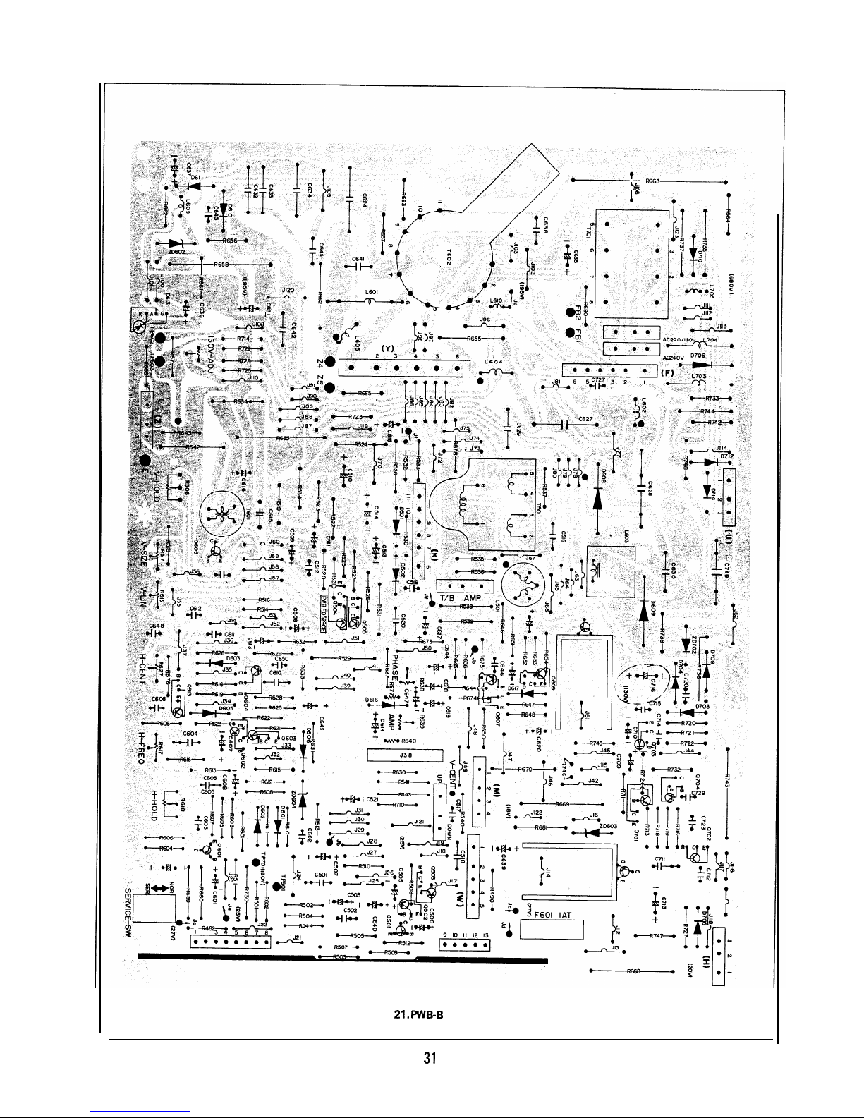
Figure
Wiring Side
Page 32

Page 33

Figure 26.
Component Side
Figure 27.
Wiring Side
Page 34

Figure 28. PWM-A Component Side
Figure 29. PWM-A Wiring Side
Page 35

CHASSIS I
D-L-AMP-AD J
.
cl
0
0
cl
0
0
0
0
0
cl
0
EL
SELECTOR BUT TON
L
SWITCH
SUB-CONTRAST
PEDESTAL LEVEL SET
.
Figure 30.
Page 36

KOS25
I I
G-DRIVE
B-DRIVE
Layout
Page 37

TOUCH
BUTTON
I
CHANNEL
SENSOR
A
SPEAKER
-AMP
VIDEO
CORRECTION
REGULATOR
SIDE PIN AMP
Page 38

DIAGRAM
I
a
KILLER
AMP
AMP
I
KILLER
PULSE
AMP
AMP
AMP
I
1
VIDEO
PEDESTAL BRIGHTNESS
AMP
5
VIDEO AMP
,
4
AMP
BLANKING A MP
REGULATOI;
,C’412
--
E
Block Diagram
Page 39

Tuner
Figure
Tuner Schematic
SAFETY NOTE:
DISCONNECT THE AC PLUG FROM THE
AC OUTLET BEFORE REPLACING
PARTS
SEMICONDUCTOR
SINKS
SHOULD BE REGARDED AS PO-
TENT/AL SHOCK HAZARDS WHEN
THE CHASSIS IS OPERATING.
BOTTOM VIEW
r
NOTE
The unit of n&stance
omitted (K-1000 ohms
M-l
2
All resistors are
watt, unless
noted.
3 All capacitors MFO, unless otherwise noted P-MMFO.
Voltage Measurement Conditions
in parenthesis measured with no Signal.
2
without parenthesis measured with
w or
All the voltages in each point an?
with
Vacuum Tube Volt Meter..
Waveform Measurement Conditions
bar generator signal of 2 V peak to
applied
at base of
Video Amplifier (Q208).
bias
BOTTOM VIEW
BOTTOM VIEW
.
CA-
-L
BOTTOM VIEW
Page 40

I(51
Page 41

REPLACEMENT
PARTS
____
-----
It is recommanded to use genuine factory SHARP replacement parts to assure fine performance.
“How to order Replacement Parts”
To have your order filled promptly and correctly, please furnish the following information-s.
Model Number
Ref. No.
Part No.
Description
REF. NO.
PART NO.
DESCRIPTION
REF. NO. PART NO.
DESCRIPTION
CRT
Picture Tube and Semiconductor Complement
Picture Tube
Deflection Yoke &
Static Conv. Assy.)
Transistor, RF-Amplifier
(UHF)
Transistor, Local
oscillator (UHF)
Transistor, UHF
Amplifier
Transistor, Mixer
Transistor, Mixer
Transistor, RF Amplifier
Transistor, Local
oscillator (VHF)
Transistor, AFT Muting
Transistor, AFT Muting
Transistor, AFT Voltage
amplifier
(Cl
Transistor, Tuning
voltage amplifier
Transistor,
Band switcher
Transistor,
Band switcher
Transistor,
Switcher
Transistor,
Switcher
Transistor,
Amplifier
Transistor,
Amplifier (VHF)
(WI
Transistor, P-l F Amplifier
Transistor, 1
Video
Amplifier
Transistor, 2nd Video
Amplifier
Transistor, Sync.
Separator
Transistor, Sync.
Amplifier
Transistor, Pulse
Amplifier
Transistor, Pulse
Amplifier
Transistor, Voltage
Regulator
Transistor, 3rd Video
Amplifier
Transistor, 3rd Video
Amplifier
Transistor, 3rd Video
Amplifier
Transistor,
Video
Amplifier
(01
(Y)
(Y)
(Y)
(Y)
(Y)
(Y)
(Y)
(Y)
Transistor, 4th Video
Amplifier
Transistor, 5th Video
Amplifier
Transistor, Blanking
Transistor, Voltage
Regulator
Transistor, Vertical
Oscillator
Transistor, Vertical
Oscillator
Transistor, Vertical
Amplifier
Vertical
Amplifier
Transistor, Vertical
Drive
Transistor, Vertical
output
Transistor, Vertical
output
Transistor, Horizontal
Transistor, Horizontal
Oscillator
Transistor, Horizontal
Oscillator
Transistor, Horizontal
Oscillator
Transistor, Horizontal Drive
Transistor, Horizontal
output
Transistor, Side-pin
Amplifier
Transistor, Side-pin Drive
Transistor, Side-pin
output
Transistor, Horiz.
Centering Amplifier
Transistor, Pulse Amplifier
Transistor, Pulse Former
Transistor, Error Amplifier
Transistor, Power Regulator
Drive
Transistor, Power Regulator
Output
Transistor, Chroma
Amplifier
Transistor, Colour Gain
Control
Transistor, Red Output
Transistor, Green Output
Transistor, Blue Output
Selector
Selector
Page 42

REF. NO.
PART NO.
DESCRIPTION
REF. NO.
PART NO.
DESCRIPTION
Diode, Protector
1
Diode, Temperature
Colour Killer
Compensation
Diode, Damper
PAL-Switch
Diode, Side-pin.
1
Variable capacitance
Diode, Side-pin.
Diode
Rectifier 19OV
1
Variable Capacitance D611
Diode, Rectification
Diode
Diode, Clamping
1
Variable Capacitance
Diode, Protector
Diode
Rectifier (Power)
1
Variable Capacitance
Rectifier (Power)
Diode
Diode, Temperature
Diode
Compensation
HZ-l 1 A
Diode, Temperature
Diode
Compensation
1
Diode
Diode, Stater
1
Diode
Diode, Damper
Variable Capacitance
1
Diode, Protector
Diode
Diode
1
Diode
Diode Clamper
Diode
Diode
Diode
Diode
1
Diode
Variable Capacitance
Diode
1
Diode
Variable Capacitance
Diode
Diode
LED, Channel Indicator
LED, Channel Indicator
E SCR Protector
LED, Channel Indicator
Diode, Protector
LED, Channel Indicator
Positive Coefficient
LED, Channel Indicator
Thermistor,
LED, Channel Indicator
1
Crystal,
LED, Channel Indicator
LED, Channel Indicator
Diode
Diode
Diode
Coils
Diode
Diode L201
Diode
Choke 10pH
Diode
Diode
Choke
Diode
Choke 12pH
Diode
Choke
Diode
Diode
Diode
Diode L501
T/B Pincushion Phase
Diode
I LPOO45C
Choke
Diode
Choke
Protective Diode
Choke
Diode
Horizontal Linearity
Diode
Choke
Diode
Choke 1
Protective Diode
I LPOO5OC
Choke
Composite Detector
Choke
Diode
I
1
Protective Diode
I
Choke
Clamping Diode
Choke
Diode
Choke 10pH
Diode, Idling Bias
Choke 10pH
Diode, Idling Bias
1
Diode,
Detector
1
Diode,
Detector
Page 43

‘REF. NO.
001
PART NO.
Transformers
I
Delay Line
DESCRIPTION
Choke
Filter 15pH
Phase Shift
Peaking
Filter
Choke
Choke
Choke
Choke
Choke
Choke
Filter P-IF
Filter
Trap
Filter
Trap
Filter P-IF
Filter P-l F
Filter P-l F
Filter
MHz Trap
Filter AFT Discriminator
Filter AFT Discriminator
Filter S-l F
Filter Sound
Demodulator
Filter
MHz Trap
T/B Pincushion
Horizontal Drive
Horizontal Flyback
Chopper
Filter Chroma
MHz
Filter PAL-Output
Video (Y)
PAL
Controls
Potentiometer
ohm
Potentiometer
ohm
Potentiometer
ohm
Potentiometer
Potentiometer
ohm
Potentiometer
ohm
Potentiometer
ohm
Potentiometer
ohm
RF
ohm
Volume
ohm
Pedestal Level Setting
ohm
Sub-Contrast 1
ohm
Contrast 1 K ohm
Brightness
ohm
Hoid
ohm
REF. NO.
PART NO.
DESCRIPTION
Lenearity
ohm
Size
ohm
Frequency
ohm
Hold
ohm
Centering
ohm
Side Pincushion Phase
ohm
Side Pincushion Amp.
ohm
Focus 15M ohm
Adjustment 1 K ohm
ohm
ohm
R-Bias
ohm
G-Bias
ohm
B-Bias 5K ohm
G-Drive
ohm
B-Drive
ohm
Screen 1 M ohm
Capacitors
01 K
K
Electrolytic 1
Electrolytic
Electrolytic 1
Electrolytic 22OpF
1
Electrolytic
Electrolytic
Electrolytic 1
1
Mylar
Mylar
.053c(F
Mylar
Mylar
.47OPF
Electrolytic 1
1
Polypropylene Film
F
Electrolytic 16OV
Electrolytic
1
Polypropylene Film
Polypropylene Film
Polypropylene Film
Polypropylene Film
Polypropylene Film
.082/~F
Electrolytic Film
.OOlpF
Polypropylene Film
Electrolytic
47OpF
Electrolytic
1
Page 44

REF. NO.
PART NO. DESCRIPTION
REF. NO.
PART NO. DESCRIPTION
Electrolytic
K
Cement 33 ohm 15W 10%
Mylar
.22pF
Cement
ohm 15W 10%
.OOlpF
Metal Coating
Electrolytic 1
ohm 2W
Fuse Resistor .56 ohm
Special Capacitor 1
10%
Oxide Metal Coating
ohm 2W
ohm 7W 10%
Cement
ohm 7W 10%
Oxide Metal Coating
B
Electrolytic
22OpF
ohm 2W
Electrolytic
Cement
ohm 5W 10%
Electrolytic
Oxide Metal Coating
Polypropylene
ohm 3W
K
IOOPF
Oxide Metal Coating
.OOlpF
ohm
Cl
Electrolytic
1
Metal Coating
ohm 2W
J
Oxide Metal Coating
ohm 2W 5%
Metal Coating
ohm 2W
Resistors
Cement
ohm
10%
.
Metal Coating
ohm
Oxide Metal Coating
Cement
ohm 5W 10%
Oxide Metal Coating
Metal Coating 1 ohm
J
Oxide Metal Coating
Oxide Metal Coating
ohm 2W 5%
ohm 2W
J
Oxide Metal Coating
Oxide Metal Coating
ohm
5%
ohm 2W 5%
Oxide Metal Coating
Oxide Metal Coating
ohm
5%
ohm 2W
J
Oxide Metal Coating
Oxide Metal Coating
ohm 2W
ohm 1W 10%
Oxide Metal Coating
Oxide Metal Coating
ohm
5%
Oxide Metal Coating
Printed Wiring Board Assemblies
ohm
5%
Oxide Metal Coating
Mother-A
Mother-B
Oxide Metal Coating
CRT Bias
ohm
Channel Indicator
K
Cement
ohm 5W 10%
Power
Oxide Metal Coating
ohm 1 W 5%
Oxide Metal Coating
ohm
5%
Oxide Metal Coating
Miscellaneous Parts
Cement
ohm 5W 10%
J
Oxide Metal Coating
Front Cabinet
ohm 3W
Back Cabinet
Metal Coating
LED-Cover
Door
Oxide Metal Coating
Badge “SHARP”
Colour Mark
Cement 10 ohm IOW 10%
H
Oxide Metal Coating
Indicated Metal
Panel
Oxide Metal Coating
Knob, On-Off-Vol.
Knob, Colour, Brightness,
1
Special Resistor Contrast
Page 45

I
REF. NO.
I
PART NO.
I
DESCRIPTION
I
CESB
L5001
CEO0
RR
Touch Button
Hinge
AC Cord
Impedance Converter
Fuse
Fuse
Fuse
Fuse 1 AT
Antenna Terminal
Socket, Picture Tube
Spark Gap
Spark Gap
Spark Gap
Service Switch
Door Switch
High Voltage Rectifier Unit
Speaker
Tuner
Page 46

SHARP
 Loading...