

Sharp 6n138 Datasheet
6N138
6N138
High Sensitivity, High Speed
OPIC Photocoupler
■ Features
1. High current transfer ratio
(CTR : MIN. 300% at IF= 1.6mA
)
2. High speed response
(t
: TYP. 2 s at R
PHL
µ
= 2.2kΩ
L
)
3. Instantaneous common mode rejection
voltage( CM
: TYP. 500V/ s
H
)
µ
4. TTL compatible output
5. Overseas standard model
6. Recognized by UL, file
No. E64380.
■ Applications
1. Interfaces for computer peripherals
2. Electronic calculators, measuring instruments,
control equipment
3. Telephone sets
4. Signal transmission between circuits of
different potentials and impedances
■ Absolute Maximum Ratings
Parameter Symbol Rating Unit
Forward current I
*1
Peak forward current I
*2
Input
Peak transient forward current I
Reverse voltage V
Power dissipation P 35 mW
Supply voltage V
Output voltage V
Output
Emitter-base reverse
withstand voltage (pin 5 to 7
*3
Average output current I
)
Power dissipation P
*4
Isolation voltage V
Operating temperature T
Storage temperature T
*5
Soldering temperature T
*1 50% duty cycle, Pulse width: 1ms
*2 pulse width<=1 s, 300pps
*3 Decreases at the rate of 0.7mA /˚C if the external temperature is 25˚C or more.
*4 40 to 60% RH, AC for 1 minute
*5 For 10 seconds
µ
F
F
FM
R
CC
O
V
EBO
O
O
iso
opr
stg
sol
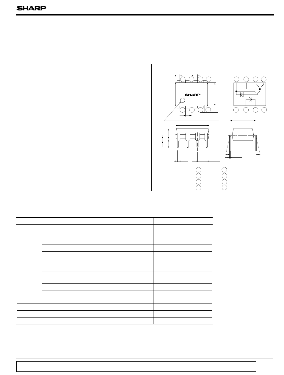
■ Outline Dimensions
9.22
± 0.1
± 0.3
1.2
± 0.5
1 NC
2 Anode
3 Cathode
4 NC
5678
0.8
2.54
)
± 0.5
6.5
± 0.2
)
± 0.25
5 GND
6 V
7 V
8 V
± 0.3
0.85
6N138
1234
± 0.3
1.2
Primary side mark (Sunken place
± 0.5
0.5TYP
3.5
± 0.5
3.7
0.5
* “OPIC ” (Optical IC) is a trademark of the SHARP Corporation.
An OPIC consists of a light-detecting element and signal processing circuit integrated onto a single chip.
(
Ta= 25˚C
(
Unit : mm
Internal connection
diagram
1234
± 0.3
7.62
= 0 to 13 ˚
θ
θ
± 0.1
0.26
O
B
CC
20 mA
40 mA
1A
5V
- 0.5 to + 7 V
- 0.5 to + 7 V
0.5 V
60 mA
100 mW
2 500
V
rms
0 to + 70 ˚C
- 55 to + 125 ˚C
260 ˚C
)
5678
θ
“ In the absence of confirmation by device specification sheets, SHARP takes no responsibility for any defects that occur in equipment using any of SHARP's devices, shown in catalogs,
data books, etc. Contact SHARP in order to obtain the latest version of the device specification sheets before using any SHARP's device.”
6N138
■ Electro-optical Characteristics
(
Ta= 0 to 70˚C unless otherwise specified
Parameter Symbol Conditions MIN. TYP. MAX. Unit
*1
Current transfer ratio
Logic (0) output voltage V
Logic (1) output current I
Logic (0) supply current I
Logic (1) supply current I
Input forward voltage V
Input forward voltage
temperature coefficient
Input reverse voltage BV
Input capacitance C
*3
Leak current
(
input-output
*3
Isolation resistance (input-output)
*3
Capacitance (input-output
)
)
*1 Current transfer ratio is a ratio of input current and output Note) Typical value : at Ta= 25˚C, V
current expressed in %.
/∆ Ta
*2 ∆ V
F
*3 Measured as 2-pin element (Short 1, 2, 3, 4 and 5, 6, 7, 8.
■ Switching Characteristics
I
CTR
F
= 4.8mA, V
OLIO
= 0, VCC=VO= 7V - 0.1 250 A
OHIF
= 1.6mA, V
CCLIF
CCHIF
*2 I
I
R
C
= 0, VCC= 5V, VO= open - 10 - nA
= 1.6mA, Ta= 25˚C
FIF
= 1.6mA
F
=10µA, Ta= 25˚C 5.0 - - V
RIR
VF= 0, f= 1MHz - 60 - pF
IN
Ta= 25˚C, 45%RH, t= 5s
I-O
V
I-O
I-OVI-O
f= 1MHz - 0.6 - pF
I-O
= 0.4V, V
O
= 4.5V, IF= 1.6mA
CC
CC
= 3kV DC
= 500V DC - 10
= 4.5V= 1.6mA, V
CC
= open= 5V, V
O
300 - %
1 600
- 0.1 0.4 V
- 0.5 -
- 1.5 1.7 V
- - 1.9 -
- - 1.0 A
12
)
(
Ta= 25˚C, V
- Ω
CC
Parameter Symbol Conditions MIN. TYP. MAX. Unit
*4
Propagation delay time
Output (1) → (0
*4
Propagation delay time
)
Output (0)→ (1)
*5
Instantaneous common mode
*6
rejection voltage “ Output (1)”
*5
Instantaneous common mode
*6
rejection voltage “ Output (0)”
t
t
CM
CM
PHL
PLH
*5 Instantaneous common mode rejection voltage “ output (1)” represents a common mode voltage variation that can hold
the output above (1) level (VO> 2.0V).
Instantaneous common mode rejection voltage “ output (0)” represents a common mode voltage variation that can hold
the output above (0) level (V
< 0.8V).
O
= 1.6mA
I
F
RL= 2.2kΩ
= 1.6mA
I
F
RL= 2.2kΩ
IF= 0, VCM= 10V
H
RL= 2.2kΩ
= 1.6mA, V
I
F
L
RL= 2.2kΩ
CM
P-P
= 10V
- 2 10 s
- 7 35 s
- 500 - V/ s
P-P
- - 500 - V/ s
µ
mA
mV/˚C
µ
=5V
CC
=5V
µ
µ
µ
µ
)
)
*4 Test circuit for Propagation Delay Time
Pulse input
duty ratio
= 1/10
IF monitor
Pulse oscillator
I
F
100Ω
1
2
3
4
5
6
7
8
R
L
V
CC
V
O
CL= 15pF
F
I
0
O
V
1.5V
t
PHL
5V
1.5V
OL
V
t
PLH
 Loading...