

Sharp 6n136, 6n135 Datasheet
6N135/6N136
6N135/6N136
General Purpose Type
Photocoupler
■Features
1. High speed response t
(6N135:MAX. 1.5µs at R
(6N136:MAX. 0.8µs at R
2. High common mode rejection voltage
(CMH:TYP. 1kV/µ
3. Standard dual-in-line package
4. Recognized by UL, file No. E64380
PHL
, t
PLH
=4.1kΩ
L
=1.9kΩ
L
)
s
)
)
■Applications
1. Computers, measuring instruments, control
equipment
2. High speed line receivers, high speed logic
3. Telephone sets
4. Signal transmission between circuits of
different potentials and impedances
■Absolute Maximum Ratings (Ta=25˚C
Parameter Symbol Rating Unit
Forward current I
*1
Input
Peak forward current
Peak transient
*2
forward current
I
I
FM
Reverse voltage V
Power dissipation P 45 mW
Supply voltage V
Output voltage V
Output
Emitter-base reverse withstand voltage (Pin 5 to 7
Average output current
Peak output current I
Base current (Pin 7
)
)
V
EBO
I
OP
I
Power dissipation P
*3
Isolation voltage V
Operating temperature
T
Storage temperature T
*4
Soldering temperature
*1 50% duty cycle, Pulse width:1ms
Decreases at the rate of 1.6mA/˚C if the external temperature is 70˚C or more.
*2 Pulse width<=1µs, 300
*3 40 to 60% RH, AC for 1 minute
*4 For 10 seconds
P/S
T
F
F
R
-0.5 to+15
CC
-0.5 to+15
O
O
B
O
2 500
iso
-55 to+100
opr
-55 to+125
stg
so1
25 mA
50 mA
1A
5V
5V
8mA
16 mA
5mA
100 mW
260 ˚C
)
V
V
V
rms
˚C
˚C
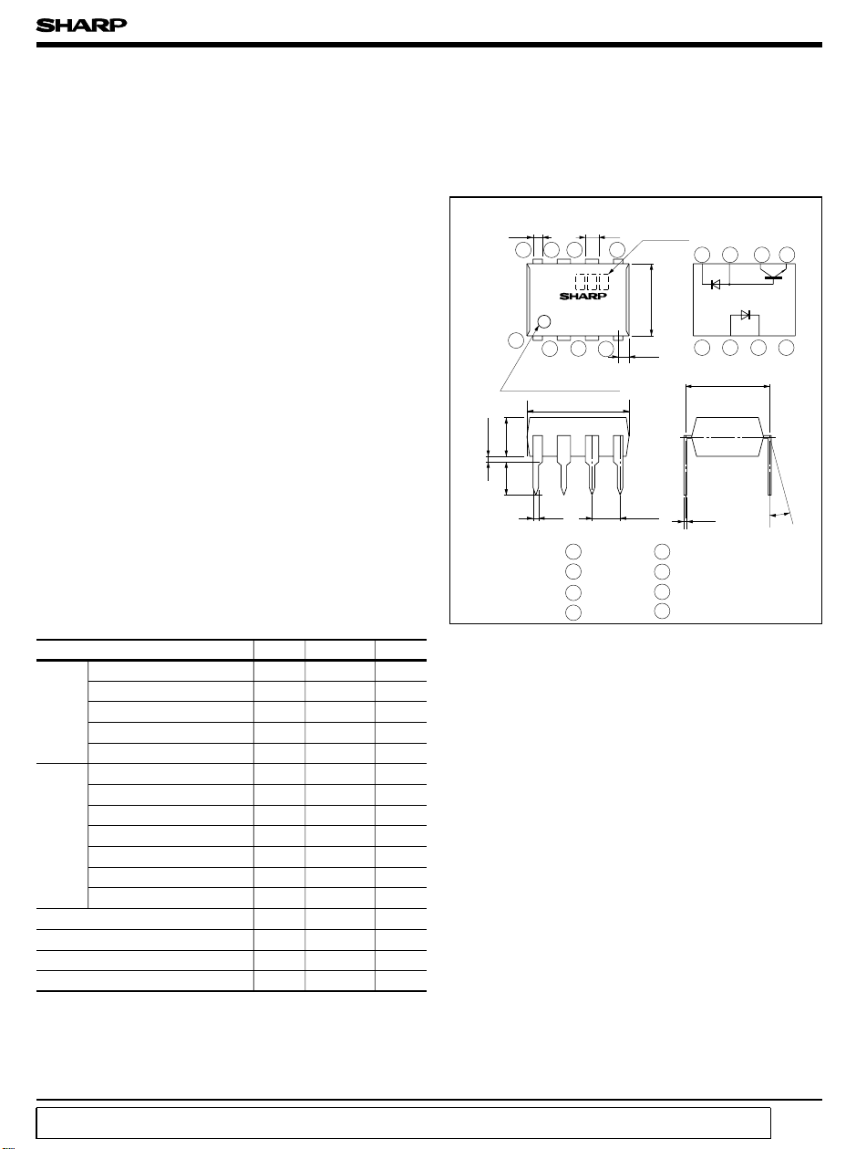
■Outline Dimensions
Model
±0.3
0.85
6N
1
234
Primary side mark
(
Sunken place
9.22
± 0.5
0.5TYP
3.5
± 0.5
3.7
* “OPIC” (Optical IC) is a trademark of the SHARP Corporation.
An OPIC consists of a light-detecting element and signal processing circuit integrated onto a single chip.
0.5
±0.1
1.2
5678
)
±0.5
1 NC
2 Anode
3 Cathode
4 NC
±0.3
2.54
No.
± 0.5
6.5
0.8
±0.25
5 GND
6 V
7 V
8 V
(
Unit:mm
Internal
connection
diagram
1234
±0.3
7.62
θ=0 to 13˚
θ
±0.1
0.26
O
B
CC
)
5678
“In the absence of confirmation by device specification sheets, SHARP takes no responsibility for any defects that occur in equipment using any of SHARP's devices, shown in catalogs,
data books, etc. Contact SHARP in order to obtain the latest version of the device specification sheets before using any SHARP's device.”
6N135/6N136
■ Electro-optical Characteristics
Parameter Symbol Conditions MIN. TYP. MAX. Unit
*5
Current transfer
ratio
6N136 CTR(1
6N135 CTR(2
6N136 CTR(2
Logic (0) output voltage V
Logic (1) output current
Logic (0) supply current I
Logic (1) supply current
Input forward voltage V
Input forward voltage
temperature coefficient
Input reverse voltage BV
Input capacitance C
6N135 CTR(1
*6
Leak current
(
input-output
*6
Isolation resistance
(
input-output
*6
Capacitance (input-output
)
)
)
Transistor current
amplification factor
*5 Current transfer ratio is the ratio of input current and output
current expressed in % .
*6 Measured as 2-pin element (Short 1, 2, 3, 4
*7 6N135 :IO= 1.1mA, 6N136 :IO= 2.4mA
)
Ta = 25˚C, IF= 16mA
)
V
O
)
)
OL
(1)
I
OH
(2)
I
OH
(3)
I
OH
CCL
(1)
I
CCH
(2)
I
CCH
F
/ ∆TaIF= 16mA - - 1.9 - mV/˚C
∆V
F
R
IN
I
I-O
R
I-O
C
I-O
h
FE
= 16mA, VO= 0.5V
I
F
V
CC
*7
IF= 16mA, VCC= 4.5V - 0.1 0.4 V
=25˚C, IF=0
T
a
V
CC=VO
=25˚C, IF=0
T
a
V
CC=VO
= 0, VCC=VO= 15V - - 50 A
I
F
IF= 16mA, VCC= 15V
V
O
=25˚C, VCC= 15V
T
a
V
F
V
CC
V
O
Ta=25˚C, IF= 16mA - 1.7 1.95 V
Ta=25˚C, IR= 10 A 5.0 - - V
VF= 0, f = 1MHz - 60 T
= 25˚C, 45 %RH, t = 5s
a
V
I-O
V
I-O
f = 1MHz - 0.6 VO= 5V, IO= 3mA - 70 -
)
(
Ta = 0 to + 70˚C unless otherwise specified
7.0 40 - %
= 0.4V, VCC= 4.5V
19 40 - %
5.0 43 - %
= 4.5V
= 5.5V
= 15V
= open
= open, IO=0
= 15V
= open, IF=0
15 43 - %
- 3.0 500 nA
- 0.01 1.0 A
- 200 - A
- 0.02 1.0 A
- - 2.0 A
µ
= 3kVDC
- - 1.0 A
= 500VDC - 10
Note) Typical volue : at Ta = 25˚C
)
µ
µ
µ
µ
µ
pF
µ
12
- Ω
pF
 Loading...