50Hz
Chassis
Colour Television
DA100 and DW100


Colour Television – DA100/DW100 Chassis
Contents
POWER SUPPLIES...........................................................................................................................1
Switch Mode Power Supply......................................................................................................1
Start up operation...........................................................................................................1
Voltage regulation ..........................................................................................................2
Over-voltage Protection..................................................................................................2
Over-current control .......................................................................................................2
Slave Processor Power Supply.................................................................................................3
Degauss Circuit........................................................................................................................ 4
5v Regulator ............................................................................................................................5
DA100 (59ESD7H and 66ESD7H) 4:3 chassis................................................................ 5
DW100 (56FW53H to 6FW54H) 16:9 chassis.................................................................6
CLASS D OUTPUT STAGES............................................................................................................7
Tda7480 Pin Functions.............................................................................................................7
Pin 9 – Frequency..........................................................................................................7
Pin 12 – Mute/Standby function......................................................................................7
Audio Output............................................................................................................................8
Field Output.............................................................................................................................9
Vertical Fly-back...........................................................................................................10
VIDEO AND SYNC PROCESSOR...................................................................................................11
Description.............................................................................................................................11
Analogue front-end.......................................................................................................11
Input Selector............................................................................................................... 11
Clamping......................................................................................................................11
Automatic Gain Control ................................................................................................12
Analogue-to-Digital Converters..................................................................................... 12
Digitally Controlled Clock Oscillator .............................................................................. 12
Analogue Video Output ................................................................................................12
Average Beam Current Limiting.................................................................................... 12
Protection Circuitry.......................................................................................................12
Scan Velocity Modulation Output..................................................................................12
PICTURE ROTATION......................................................................................................................13
SCAN VELOCITY MODULATOR .................................................................................................... 14
LINE OUTPUT STAGE.................................................................................................................... 15
East West Circuit.................................................................................................................... 16
Circuit Description........................................................................................................16
MICROPROCESSOR CONTROL....................................................................................................17
Reset.....................................................................................................................................18
PROTECTION.................................................................................................................................19
Microprocessor....................................................................................................................... 19
Audio Output................................................................................................................19
Beam Current...............................................................................................................19
Horizontal Mute............................................................................................................19
Video/Sync Processor............................................................................................................20
Safety ..........................................................................................................................20
Vprot............................................................................................................................20
Sharp Electronics (UK) Ltd
September 99
Technical Support

Colour Television – DA100/DW100 Chassis
POWER SUPPLIES
This CTV employs two power supplies, which are similar in design to previous models. The Power
Supply located on the sub-board 'PWB-C' will supply the Dolby Prologic circuit and Audio Output
Stages that are also located on PWB-C. Similar to the CS, CA10 and CW100 chassis, when this
receiver is in standby mode, the outputs from the power supplies (including the supply to the Main
Microprocessor circuit) will be muted by removal of the FET gate voltage. The Slave Processor
(IC702) performs standby and timer on/off functions, additionally in this chassis the Slave Processor
will control the degauss circuit.
SWITCH MODE POWER SUPPLY
+8v
D721
8v2
+16v
-16v
150V
R743
47k
R744
47k
R746
47k
D730
Standby
R719
220
C712
100pF
D712
15v
D713
Q702
+HT
R713
560k
R714
560k Q701
R717
22k
Q703
C738
56pF
R716
0R47
C711
330pF
C714
82nF
C713
68nF
R730
82
C715
330pF
R723
270
R715
47k
D711
To Degauss
Circuit
R718
18
D716
5v6
C717
15nF
C718
3n3
C710
47nF
D715
R722
0R33
T701
17
12
14
8
7
3
4
5
6
115
2
IC705
R724
470
IC706
R728
180
D718
D719
D720
D726
12v
R750
1M
R727
180
C718
1000
C719
1000
C720
100
R766
220
R765
220
R745
1k8
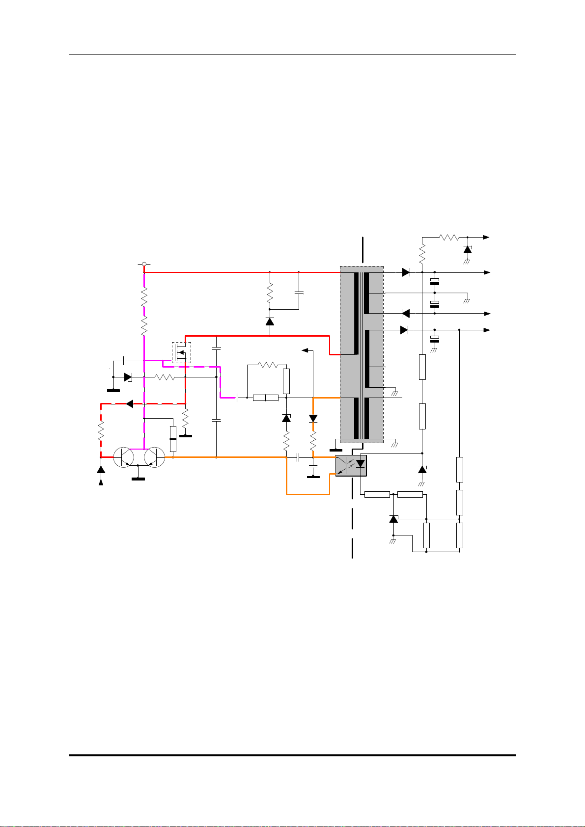
START UP OPERATION
Rectified and smoothed mains voltage (+320VDC) is used to provide the start up voltage to the gate
of Q701. Current flows via R713 and R714 charging C714 (C714 earth return is via T701 secondary
winding pins 14 and 15). This allows a voltage at the gate of Q701 to rise slowly (Q701 will turn on
when the gate reaches 4.5V). D712 ensures that Q701 gate voltage will not exceed 15V, preventing
the FET being damage by voltage spikes.
When Q701 turns on, current will flow from the bridge rectifier, through T701 primary winding (pins 12
and 17), Q701 source/drain junction, returning to the bridge rectifier via, R716. The current flowing
through T701 primary will induce an e.m.f. into secondary windings
The e.m.f. produced at T701 pin 15 will flow through D715 and the collector emitter junction of the
opto-coupler (IC705), charging C713. Once the charge on C713 reaches 0.6V Q703 will turn on,
connecting Q701 gate to ground, turning Q701 off and discharging C714.
Sharp Electronics (UK) Ltd
September 99 Page 1
Technical Support

Colour Television – DA100/DW100 Chassis
At this point, the magnetic field within T701 will collapse causing the e.m.f at pin 15 to go negative
turning Q703 off.
Q701 will not turn on until sufficient charge has built up on C714. However, at this time the negative
plate of C714 is approximately -12V; due to the collapsing field within T701. This results in the time
period required to build sufficient charge on C714 to bias Q701 on increasing i.e. Q701 off time = the
time for the back 'e.m.f.' to decade to zero, plus C714 charge time form zero to 4.5V approx.).
VOLTAGE REGULATION
The feed back through the opto-coupler (IC705), provides voltage regulation. The +150V line is used
as the controlling source and a reference is provided from the +16v supply.
Increase in load
As the +150V rail falls due to an increase in load (high beam current), the trigger voltage of IC706 will
fall, increasing IC706 cathode voltage, reducing the current flowing through the LED section of IC705.
This has the effect of decreasing the conduction of the photo transistor part of IC705. This increases
the voltage drop across the collector/emitter junction; thereby increasing the time taken to charge
C713, delaying the point when Q703 turns on, turning Q701 off. Energy is transferred across T701 for
a longer period, increasing the HT rail; hence, the frequency of the power supply will fall.
Decrease in load
As the +150V rail increase due to a decreasing load (low beam current), the trigger voltage of IC706
will rise decreasing IC706 cathode voltage which increases the current flow through the LED section
of IC705. This has the effect of increase the conduction of the phototransistor within IC705. Thereby
decreasing the voltage drop across the collector/emitter junction; which will decrease C713 charge
time, advancing the point when Q703 turns off, turning off Q701 to turn on earlier. Energy is
transferred across T701 for a shorter period, decreasing the HT rail; hence, the frequency of the
power supply will increase.
It can now be seen that this is a variable frequency power supply, typically the frequency will vary
between 144kHz (no load) to 70kHz (high beam current).
OVER-VOLTAGE PROTECTION
D716 is used to prevent the secondary rails increasing beyond safe limits. If the e.m.f. at T701 pin 15
increases beyond safe limits D716 will conduct, increase the voltage across C713, thereby reducing
its charge time, turning on Q703 earlier, turning off Q701, allowing the HT rails to fall. Once the HT
starts to fall Q703 will turn off allowing the Power Supply to restart.
OVER-CURRENT CONTROL
Over current control is performed by monitoring the amount of current passing though the R716
(Q701 drain, earth return resistor). This resistor is an extremely low value, 0.47R, and Ohms Law
dictates that the current flowing through it must be proportional to the voltage across it. The base
voltage required for turning on Q702, is +0.6V then the voltage across R706 to ‘trip’ the circuit would
have to be approximately 1.2V (this includes 0.6V drop across D720). Therefore a current of 2.5amps
is required to operate the trip circuit.
The voltage developed across R716 will turn Q702 on via D713 and R719. Once Q702 turns on,
C714 will discharge rapidly, removing Q701 gate bias. Q701 will remain turn off until the current
through R716 decreases. At this point Q702 turns off allowing C714 to charge turning on Q701. If the
overload is still present then Q702 will turn on again, thus repeating the cycle. In the case of a short
circuit line output transistor the power supply will keep repeating this cycle. The HT rail and base of
Q702 (if measured with a standard DVM) would normally read zero volts and the power supply
appears not to be working. On some occasions when the short is not as heavy then a whistle may be
heard.
Sharp Electronics (UK) Ltd
September 99 Page 2
Technical Support

Colour Television – DA100/DW100 Chassis
SLAVE PROCESSOR POWER SUPPLY
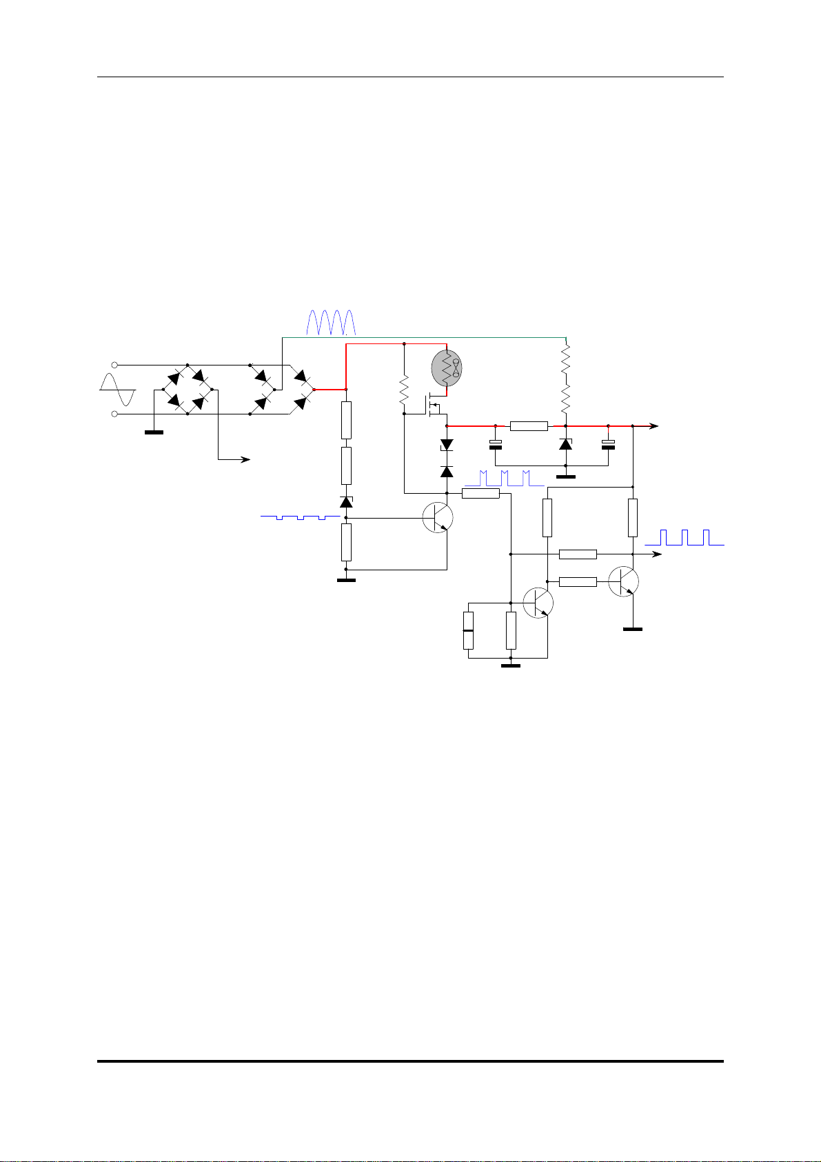
This part of the circuit has changed compared to previous chassis, where this supply was derived by
means of a bridge rectifier with two additional 68k resistors and a 5v1 zener diode to limit the voltage.
This has been replaced by a series regulator circuit, which is supplied from one side of the mains, with
an earth return via the bridge rectifier.
D708 and D707 forms part of a bridge rectifier, two diodes of the main bridge rectifier are used for the
other part. Therefore, at the junction of D707 and D708 there is a 100Hz signal comprising of positive
halve cycles at mains potential. Each time this signal exceeds 47v D729 will conduct, turning on
Q717.
D710
5v1
R738
47k
R737
180k
R721
150k
R703
150k
+5v
C724
220
R739
47k
R736
470k
Clock
D734
D731
HT
D707
D708
R774
470k
R775
470k
D729
47v
R776
82k
R771
470k
D732
15v
D733
Q717
Q715
C739
220
R770
220
R735
470k
C725
4n7
R777
47
Q708 Q709
R787
47k
When Q717 turns on the gate of Q715 is taken to ground. Since this is a N Channel MOSFET Q715 is
turned off and no current will flow through this device.
During the period when Q717 is turned off Q715 will turn on allowing C739 to charge to approximately
7v which is limited to 5v by R777 and D710.
It can now be seen that the period of Q715 conduction is very short (it is only turned on when the
100Hz signal at the junction of D707 and D708 is less than 47v). Therefore, a top-up supply from the
bridge rectifier circuit comprising of D734 and D731 is added to the cathode of D710 via R721 and
R703.
The 100Hz signal at the junction Q717 and D733 is also used as a timing signal for the real time clock
within the slave processor. However, before it can be used the signal is passed through a Schmitt
Trigger circuit (Q708 and Q709) to ensure that the signal free from noise.
Sharp Electronics (UK) Ltd
September 99 Page 3
Technical Support

Colour Television – DA100/DW100 Chassis
DEGAUSS CIRCUIT
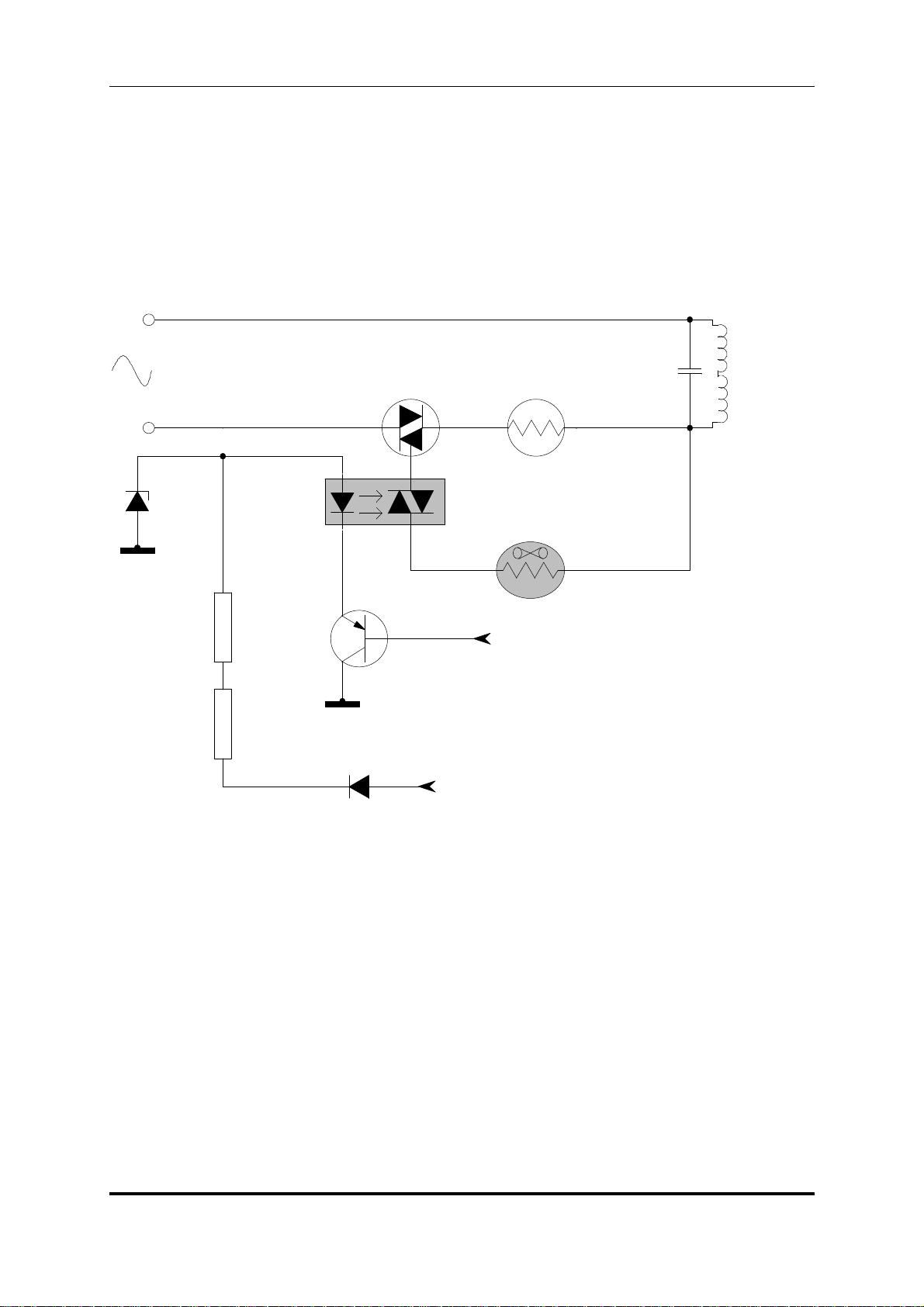
This circuit is configured to ensure that the degauss circuit will not operated unless the switch mode
power supply is operating and IC702 pin 14 = low.
A positive bias is applied to the emitter of Q714 from T701 pin 15 (rectified by D727 and limited by
D728). Via the opto-coupler; IC708. Since Q714 is a pnp device once the base is taken low compared
to the emitter, Q714 will turn on allowing current to flow through IC708 (LED Section), turning on the
triac T702, allowing current to flow through the degauss coils.
N
L
D728
4v7
R768
220
R762
220
Q714
IC708
D727
T702
POR701
R763
100
From IC702
pin 14
From T701
pin15
C702
10nF
Degause
Coils
Current will continue to flow through the degauss coils until either the PTC (POR701) has increased in
value sufficiently to cut off the current flow, or IC702 pin 14 goes high, turning of Q714, preventing
current flow through IC708, turning the triac T702 off.
Since the default condition for IC702 = low, it can be seen that the degauss circuit should now operate
each time the CTV is turned on from the main on/off switch or switched from standby to normal
operation. Whether the main processor has set up communication with the slave processor or not.
Sharp Electronics (UK) Ltd
September 99 Page 4
Technical Support

Colour Television – DA100/DW100 Chassis
5V REGULATOR
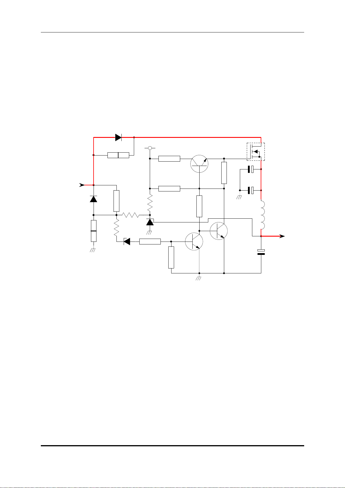
This is another new circuit, but depending on whether you are dealing with the DA100 (4:3) chassis or
DW100 (16:9) chassis will determine the exact circuit.
DA100 (59ESD7H AND 66ESD7H) 4:3 CHASSIS
The FET Q704 is a series regulator producing 5v, which is controlled by Q713. A voltage is fed-back
from the output of Q704 (junction of L705 and C723) which will control the conduction of a variable
zener diode (IC707). D723, Q705 and Q706 provide protection against excessive supply voltage.
D722
From T701
pin 1
D714
C722
10nF
R707
1k5
R725
10k
C735
150pF
D723
2v7
R710
2k2
+16v
R731
10k
R726
22
R757
2k2
R706
8k2
IC707
R756
10k
Q713
R760
4k7
R729
4k7
Q705
Q704
C734
470
C721
470
L705
Q706
+5v
C723
2200
Sharp Electronics (UK) Ltd
September 99 Page 5
Technical Support
