

Page 1

64LHP5000
PROJECTOR UNIT
FINAL
SERVICE MANUAL
S29C764LHP5-P
REAR PROJECTION HDTV
MODEL
In the interests of user-safety (Required by safety regulations in some countries) the set should be restored
to its original condition and only parts identical to those specified should be used.
64LHP5000
OUTLINE
1.This manual covers the 64LHP5000 Projector unit. The DTV Decoder is referred to in the DTV Unit Service
Manual that will be separately issued.
2.The Projector Unit Service Manual consists of two books: Issue No. S29C764LHP5-P and Issue No.
S29C864LHP5-P Use these two books together for serivicing.
CONTENTS
Page Page
〈
Issue No. S29C764LHP5-P
SPECIFICATIONS..............................................2
SAFETY INFORMATION...................................3
OPERATION MANUAL......................................6
ADJUSTMENT.................................................13
GENERAL INFORMATION..............................50
BLOCK DIAGRAMS.......................................102
SCHEMATIC DIAGRAM.................................108
PCB CONNECTION DIAGRAM.....................220
〉
〈
Issue No. S29C864LHP5-P
PARTS LIST
ELECTRICAL PARTS...............................244
CABINET AND MECHANICAL PARTS....320
PACKING OF THE SET.................................341
〉
SHARP CORPORATION
This document has been published to be used for
after sales service only.
The contents are subject to change without notice.
1
Page 2

64LHP5000
PROJECTOR UNIT
Specifications
Display and amplifier section
Screen size ..................................................................... 64"
CRT.................................................. 7" High focus CRT x 3
Brightness (White peak) ......................... 400 Foot-Lamber t
[White window signal input contrast Max.]
without protective screen
Horizontal resolution.......................... More than 1400 lines
[Input digital test pattern (1400 lines resolution)]
Input terminals ...............................................4 video inputs
4 S-VIDEO input jacks (Y/C separate INPUT)
2 COMPONENT VIDEO INPUT jacks (Y, C
CENTER INPUT jack
Output terminals ..................................... MONITOR/AUDIO
Input terminal signal ratings
Input signal
Video signal:
Composite and S-VIDEO(Y): 1.0 Vp-p (75 ohms
load)
COMPONENT (Y):1.0 Vp-p (75 ohms load)
B/PB, CR/PR):0.7 Vp-p (75 ohms load)
(C
Audio signal (including CENTER): 500mV rms
Input impedance............................. Video input: 75 ohms
Audio input (including CENTER): 22 kilo-ohms
Input signal polarity (Video) ........ Synchronized negative
Output terminal signal ratings
Output signal .......... Video signal: 1 Vp-p (75 ohms load)
Audio signal: 500 mV rms (100 % modulation)
Output impedance ........................ Video output: 75 ohms
Audio output: Less than 1 kilo-ohms
Effective output
Front both channels driven............................. 15 W + 15 W
(THD. 1 % 1 kHz, 8 ohms)
Built-in speaker system ...... 16 cm (6-5/16 in) full range x 2
..............................................6.6 cm (2-9/16 in) tweeter x 2
DTV-OUT (NTSC)................... Audio: 2 Vrms (1 kHz, 0 dB)
Video: Composite Video; 1.0 Vp-p (Negative sync on), 75
Audio output
5.1 ch output..............................Front L/R, surround L/R,
center and subwoofer
Output connector: Pin-jack
Digital audio I/F . Optical digital output: Optical connector
Coaxial digital output........................................... Pin-jack
IR-MOUSE G-LINK Terminal x 1
Digital expansion port ............. For expansion input devices
B/PB, CR/PR)
4 audio inputs
or more
Tuner section
Circuit type...................................... Video signal detection:
PLL full synchronous detection
PLL digital synthesizer system
Audio multiplex: ATSC system
NTSC Reception channels
VHF; CH2–CH13, UHF; CH14–CH69
CATV (STANDARD, IRC or HRC)
CATV 1-125 CH
DTV reception channels
VHF: Low 54–88 MHz, High 174–216 MHz,
UHF: 470–806 MHz
Antenna terminals
................................... Antenna terminal, 75 ohms UNBAL,
F-type connector (VHF, UHF MIXED)
Electrical section, miscellaneous
Power requirements...................................120 V AC, 60 Hz
Power consumption ................................................... 400 W
External dimensions .... 1510 (W) x 698 (D) x 1425 (H) mm
59-7/16 (W) x 27-31/64 (D) x 56-1/8 (H) inch
Weight of main unit.............................. 167 kg (368 lb 4 oz)
NOTE:
Specifications and design are subject to possible modifications
without notice due to improvements.
2
Page 3

64LHP5000
PROJECTOR UNIT
SAFETY INFORMATION
This service manual is intended for qualified service technicians; it is not meant for the casual do-ityourselfer. Qualified technicians have the necessary test equipment and tools, and have been trained to
properly and safely repair complex products such as those covered by this manual.
Improperly performed repairs can adversely affect the safety and reliability of the product and may void the
warranty. If you are not qualified to perform the repair of this product properly and safely, you should not risk
trying to do so and refer the repair to a qualified service technician.
WARNING
This product contains lead in solder and certain electrical parts contain chemicals which are known to the state of
California to cause cancer, birth defects or other reproductive harm.
Health & safety code section 25249.6—Proposition 65
NOTES
(FOR CANADIAN MODEL ONLY)
Fuse symbols (fast operating fuse) and/or (slow operating fuse) on PCB indicate that replacement parts must be
of identical designation.
REMARQUE
(POUR MODÈLE CANADIEN SEULEMENT)
Les symboles de fusible (fusible de type rapide) et/ou (fusible de type lent) sur CCI indiquent que les pièces de
remplacement doivent avoir la même désignation.
SAFETY PRECAUTIONS
NOTlCE: Comply with all cautions and safety related notes
located on or inside the cabinet and on the chassis or picture
tube.
The following precautions should be observed:
1. Do not install, remove, or handle the picture tube in any
manner unless shatterproof goggles are worn. People
not so equipped should be kept away while picture tubes
are handled.
Keep picture tube away from the body while handling.
2. When service is required, even though the PROJECTION MONITOR RECEIVER an isolation transformer
should be inserted between power line and the set in
safety before any service is performed.
3. When replacing a chassis in the set, all the protective
devices must be put back in place, such as barriers,
nonmetallic knobs, adjustment and compartment
covershields, isolation resistor-capacitor, etc.
4. When service is required, observe the original lead
dress.
Extra precaution should be taken to assure correct lead
dress in the high voltage circuitry area.
5. Always use the manufacturer’s replacement components. Especially critical components as indicated on the
circuit diagram should not be replaced by other
manufacture’s.
Furthermore where a short circuit has occurred, replace
those components that indicate evidence of overheating.
6. Before returning a serviced set to the customer, the service technician must thoroughly test the unit to be certain
that it is completely safe to operate without danger of
electrical shock, and be sure that no protective device
built into the set by the manufacturer has become defective, or inadvertently defeated during servicing.
Therefore, the following checks should be performed for the
continued protection of the customer and service technician.
Leakage Current Cold Check
With the AC plug removed from 120V AC 60Hz source,
place a jumper across the two plug prongs. Turn the AC
power switch on. Using an insulation tester (DC 500V), connect one lead to the jumpered AC plug and touch the other
lead to each exposed metal part (input/output terminals,
screwheads, metal overlays, control shafts, etc.), particularly any exposed metal part having a return path to the
chassis. Exposed metal parts having a return path to the
chassis should have a minimum resistor reading of 0.3MΩ
and a maximum resistor reading of 5MΩ. Any resistor value
below or above this range indicates an abnormality which
requires corrective action. Exposed metal parts not having a
return path to the chassis will indicate an open circuit.
3
Page 4

64LHP5000
PROJECTOR UNIT
Leakage Current Hot Check
Plug the AC line cord directly into a 120V AC 60Hz outlet ( do
not use an isolation transformer for this check). Turn the AC
power switch on.
Using a “Leakage Current Tester (Simpson Model 229
equivalent )”, measure for current from all exposed metal
parts of the cabinet ( input/output terminals, screwheads,
metal overlays, control shaft, etc. ), particularly any exposed
metal part having a return path to the chassis, to a known
earth ground (water pipe, conduit, etc.). Any current measured must not exceed 0.5mA.
Reading should
not be above
0.5 mA
Earth ground
Device
under
test
2-wire cord
Also test with
plug reversed
(Using AC adapter
plug as required)
Test all
exposed metal
surfaces
Leakage
current
tester
AC Leakage Test
ANY MEASUREMENTS NOT WITHIN THE LIMITS OUTLINED
ABOVE ARE INDICATIVE OF A POTENTIAL SHOCK HAZARD
AND MUST BE CORRECTED BEFORE RETURNING THE SET
TO THE CUSTOMER.
High V oltage
This set is provided with a X-ray protection for clearly indicating that voltage has increased in excess of a predetermined value. Comply with all notes described in this Service
Manual regarding this hold down circuit when servicing, so
that this X-ray protection may correctly by operated.
Serviceman Warning
In the status of the black picture ( video muting is being applied ) when no signal is input, high voltage of this set during
operation is less than 30.5kV. In case any component having some relation to the high voltage is replaced, confirm
that the high voltage is lower than 30.5kV in the status of the
black picture when no signal is input.
To measure H.V. use a high impedance H.V. meter.
Connect ( – ) to earth and ( + ) to the FBT anode cable connector.
(Refer to page 50)
X-radiation
TUBE: The primary source of X-radiation in this set is the
picture tube.
For continued X-radiation protection, the replacement tube
must be the same type as the original, SHARP approved
type.
The picture tube (the CRT assy R, G, B ) use in this set
holds complete guarantee against X-ray radiation when the
X-ray is sealed (See page 5). Accordingly, when the current
in flowing to the picture tube (CRT assy R, G, B) be sure to
perform it by putting the tube into X-ray sealed applied state.
Avoid absolutely to flow the current to the picture tube (CRT
assy R, G, B) itself. Moreover, when the voltage of the high
voltage circuit becomes abnormally a little higher, the picture tube radiates X-rays. Accordingly, when servicing the
high voltage circuit be sure to replace as an assembly with
the DEFLECTION SERVICE assy in the manner in which
has been adjusted to perform normal operation.
PRODUCT SAFETY NOTICE
Many electrical and mechanical parts in SHARP set have
special safety related characteristics. These are often not
evident from visual inspection nor the protection afforded by
them necessarily can be obtained by using replacement
components rated for higher voltage, wattage, etc. Replacement parts which have these special safety characteristics
are identified in this Service Manual.
Electrical components having such features are identified by
marking with a å on the schematics and on the parts list in
this Service Manual.
The use of a substitute replacement component which does
not have the same safety characteristics as the SHARP recommended replacement one, shown in the parts list in this
Service Manual, may create shock, fire, X-radiation, or other
hazards.
Product Safety is continuously under review and new instructions are issued from time to time. For the latest information, always consult the current SHARP Service Manual.
A subscription to, or additional copies of SHARP Service
Manual may be obtained at a nominal charge from SHARP.
4
Page 5
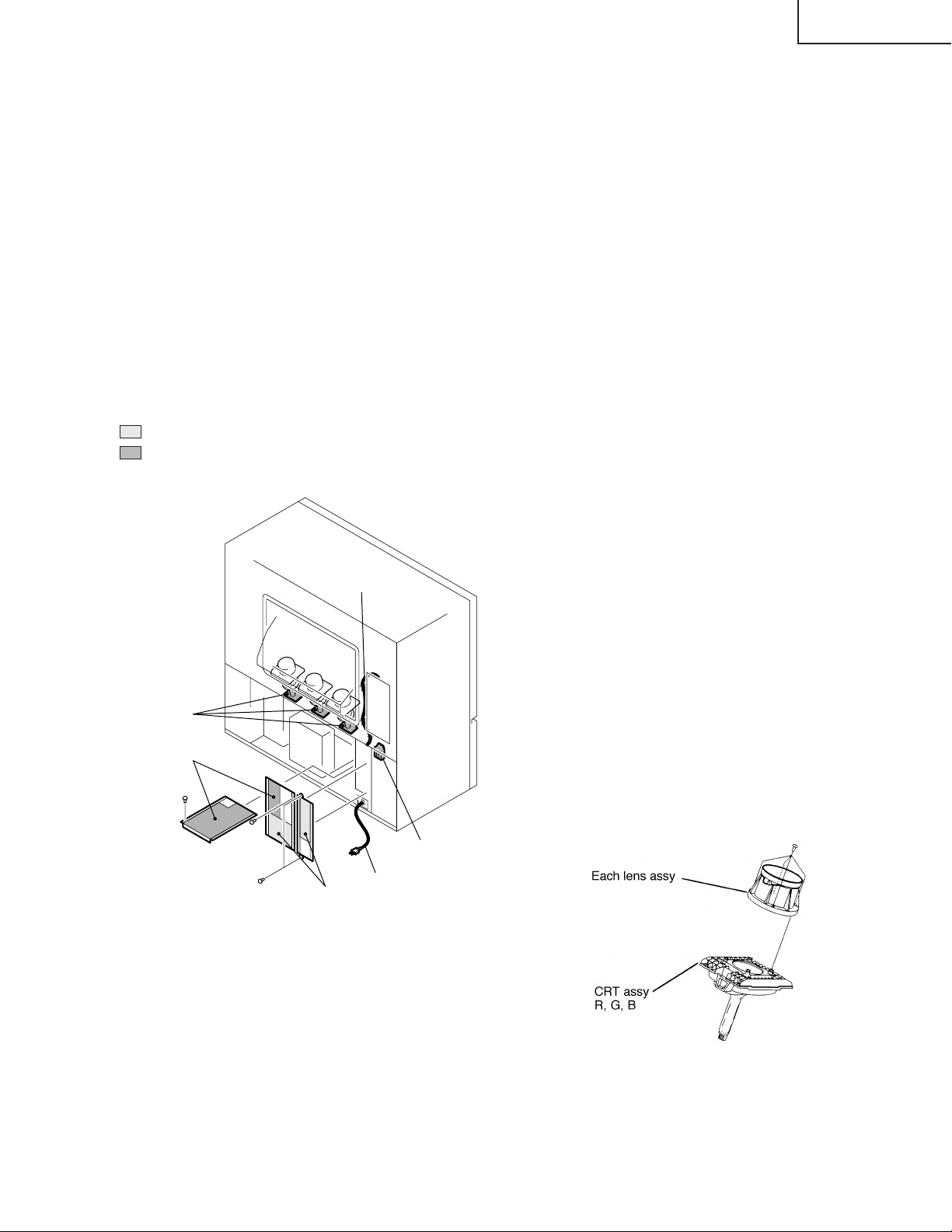
CHARGED SECTION, HIGH VOLTAGE GENERATING POINT
AND X-RAY PROTECTION
Ë
Charged section
The circuit in which the commercial AC power is used as it
is without passing through the power supply transformer. If
the charged section is touched, there is a risk of electric
shock. In addition, the measuring equipment can be damaged if it is connected to the GND of the charged section
and the GND of the non-charged section while connecting
the set directly to the commercial AC power supply. In this
case, be sure to connect the set via an insulated transformer
and supply the current.
Ë
Charged section
(Power supply primary side)
1. The primary side of the AC IN assy
2. AC power cord
3. The primary side of the POWER SUPPLY assy
4. AC power cord for DTV STB
: Part is the charged section.
: Part is the high voltage generating
points other than the charged section.
AC power cord for
DTV STB
High Voltage
generating point
High Voltage
generating point
Ë
High voltage generating point
The place where voltage is 100V is generated.
1. Charged seciton
DEFLECTION assy
(including FBT) (30.5kV, 1.2kV, 210V,135V)
2. POWER SUPPLY assy (135V)
3. R. CRT DRIVE assy (10.5kV, 210V)
4. G. CRT DRIVE assy (10.5kV, 210V)
5. B. CRT DRIVE assy (10.5kV, 210V)
6. CRT assy R (CRT service assy R) (30.5kV)
7. CRT assy G (CRT service assy G) (30.5kV)
8. CRT assy B (CRT service assy B) (30.5kV)
9. Focus variable resistor(VR1) (10.5kV)
10. Deflection yokes (L1, L2 and L3) Approx. (1100V at peak)
Ë
X-ray protection
• Regarding the parts which are relative to radiation of X-
rays (There is the danger to radiate X-ray from the individual CRT assy R, G, B), there are notifications of caution in the individual schematic diagrams. Be sure to read
them for safety’s sake.
• The component parts for X-ray protection are as follows :
When the current flows to the CRT assy R, G, B, be sure
to perform it with these parts being attached. Protection
from the X-ray radiation is maintained in the state in which
these parts have been installed to the CRT assy. R, G, B.
Accordingly, never supply current only to the CRT assy R,
G, B.
Moreover, the anode voltage of the CRT assy R, G, B
should always be kept not higher than the predetermined
value (in the minimum brightness and picture state when
non signal input is less than 30.5kV). Be sure to drive the
CRT assy R, G, B by using a completely functional DEFLECTION assy which have been adjusted completely in
the combined state. (When the voltage abnormally becomes high, the X-ray protection circuit will operate.)
1. CRT assy R, G, B (Do not dismantle CRT assemblies
under any circumastances)
2. Each Lens assy
64LHP5000
PROJECTOR UNIT
High Voltage
generating point
AC Power cord
Charged section
Fig. 1 Charged section and high voltage generating point
Fig. 2 Component parts for X-ray protection
5
Page 6
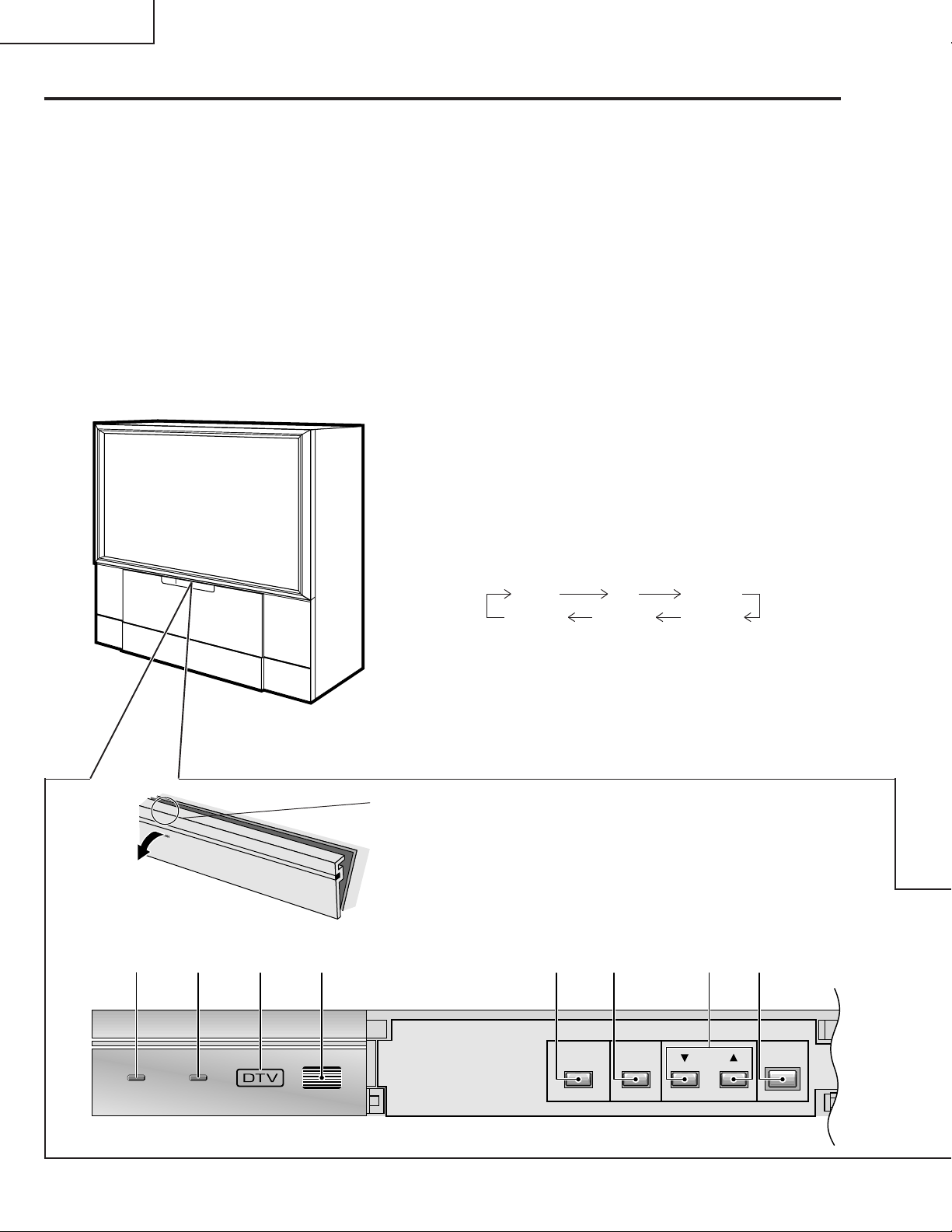
64LHP5000
POWER
STANDBY/ON
INPUT CH RETURN
POWER/
DOWN LOAD
TIMER OPC
PROJECTOR UNIT
Front Panel Functions
A flip-down door conceals the control panel. Push gently
and release, to open the door. To close the door, lift it back
up into place.
NOTE:
If you accidentally pull the door, it may not shut properly. Push the
door back in to shut it.
1 POWER/DOWNLOAD indicator
Lights when power is on. Flashes when downloading the
GUIDE Plus+ program information.
2 Timer indicator
Lights GUIDE Plus+ timer is set.
3 DTV indicator
Lights when receiving a digital television broadcast.
Flashes when downloading the DTV program information.
(DTV indicator may still blink even when the power has
been turned off. This is not a defect.)
4 OPC sensor
Sensor to detect the room brightness.
5 POWER button (ST ANDBY/ON)
Press once to turn on the Rear Projection HDTV. Press
again to turn off the Rear Projection HDTV.
NOTE:
When the Rear Projection HDTV is turned on in DTV mode, it may take
several seconds before the DTV image is displayed. This is not a
malfunction.
6 INPUT button
Press to select your program source. Each press of the
INPUT changes the selection to the next source.
TV DTV INPUT 1
INPUT 4 INPUT 3 INPUT 2
7 CHANNEL b uttons
Press plus ' or minus " to tune to a higher or lower
channel. Only the preset channels can be tuned in using
these buttons.
8 RETURN b utton
Press to set the Rear Projection HDTV to its initial mode.
In some cases, the door may only open slightly when
pushed.
In such cases, open the door with your finger as shown in
the figure at left.
51 2 3 4 6 7 8
6
Page 7
64LHP5000
VOL
S-VIDEO
INPUT 4
VIDEO L-AUDIO-R
(MONO)
PROJECTOR UNIT
FRONT PANEL FUNCTIONS
Initial mode
Input selector: Set to TV.
TV channel: Remains at the last channel set.
VOLUME: Remains at the last setting.
MUTING: OFF
VIDEO
MODE: STD
Parameters: Set to 0.
3D Y/C LEVEL: 3
3D NR LEVEL: 3
CNR: OFF
FAV. COLOR: STD.
FLESH TONE: ON
AUDIO
MTS: MAIN
Parameters: Set to 0.
SURROUND: OFF
VIEW
AUT O VIEW: OFF
MODE: SMART STRETCH
V. POSITION: Set to 0.
CC: OFF
OPC: OFF
SYSTEM IN/OUT
SPEAKER: NORMAL
AUDIO OUT: FIXED
CAUTION:
Do not press any operation button on the Rear Projection
HDTV or the remote control unit while recording. Signals
from the MONITOR OUTPUT jacks may be temporarily
interrupted when a button is pressed.
ATTENTION
The Rear Projection HDTV Receiver will not function
properly in the following cases.
• An electrical discharge in the CRT.
• Lightning storms.
• High static electricity environment.
• Poor voltage regulation in the power source.
If the Rear Projection HDTV does not operate properly,
reset it as follows:
1. Unplug the AC cord.
2. After approximately 1 minute, turn on the power with
switch and 5 POWER button.
NOTE:
On rare occasions, an electrical discharge may occur inside the
CRT. It makes a short, sharp pop and either no sound is produced
or the volume level changes by itself. The TWIN PICTURE and
SEARCH SCREEN function will be cancelled automatically if an
electrical discharge occurs when this function is engaged.
• When this button is pressed while adjusting the
outer point convergence, the outer point
convergence returns to the initial mode.
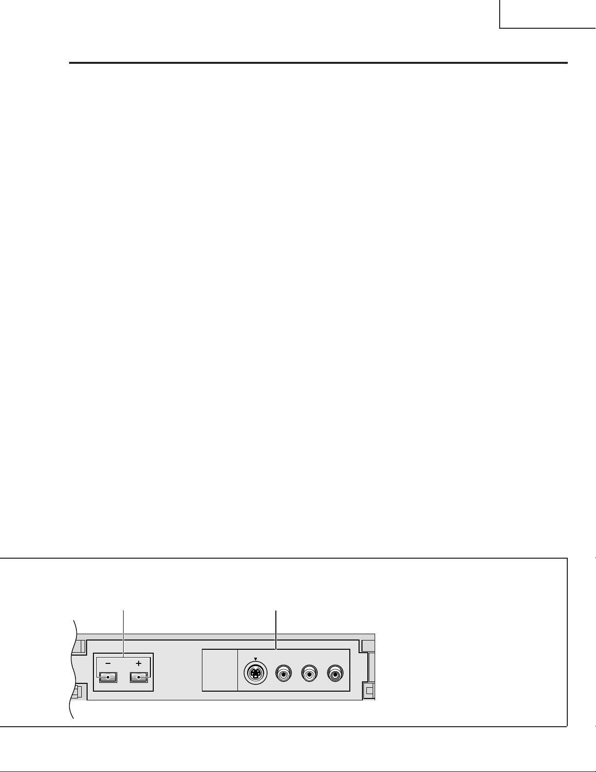
9 VOLUME buttons
Press plus (+) button to increase the volume, press minus
(–) button to decrease it.
0 INPUT 4 jac ks
These inputs are for Video Movie and VCR. Use RCA-type
pin plug cords (the same as those used in Hi-Fi systems)
and S-VIDEO cords for connections. When the audio
source to be connected is monaural, connect the source to
the L-(MONO) jack.
9 0
7
Page 8
64LHP5000
PROJECTOR UNIT
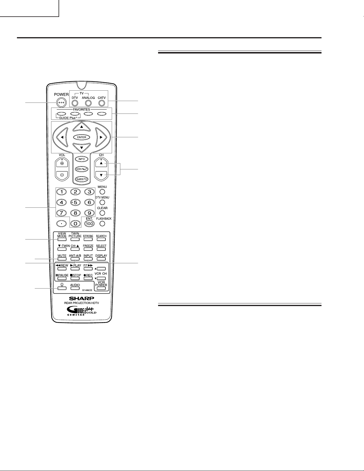
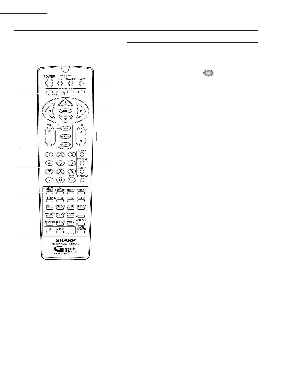
Remote Control Unit Functions
1
0
MONITOR (TV) CONTR OL B UTT ONS
1 POWER button
Turns the power of the Rear Projection HDTV on and off.
2 Input button (TV, DTV, INPUT 1 to INPUT 4)
Press the button to select the source you wish to watch. The screen
will display your selection.
5
3
4
7
9
8
6
2
3 VIEW MODE button
Press to select the VIEW MODE.
4 ANT-A/B button
Press to switch between ANTENNA-A and ANTENNA-B when you
wish to watch TV.
5 Direct channel selection buttons
Press the button (or buttons) that corresponds to the channel that
you wish to watch.
6 CH (channel) ', " button
Press plus ' or minus " to tune in a higher or lower channel. Only
the preset channels can be tuned in using these buttons.
7 MUTE button
Press to temporarily turn off the sound. Press again to return to the
previous volume level.
8 Cursor/ENTER buttons (ENTER, \, |, ', ")
\, |, ', ": Press to select or adjust items on the menu screen.
ENTER: Press to activate the selected function.
9 FAVORITES buttons
These buttons call up the channels that have been assigned to
them.
q
REMOTE CONTR OL UNIT SETTING BUTTONS
0 Remote control mode select buttons
Use to switch the remote control unit modes.
q Light button
When this button is pressed, some buttons on the remote control
unit will light. The lighting will tur n off if no operations are performed
within about six seconds.
This button is used for performing operations in dark places.
8
Page 9

a
t
s
p
i
o
u
64LHP5000
PROJECTOR UNIT
w TWIN PICTURE/SEARCH screen buttons
TWIN PICTURE: Press to turn the TWIN PICTURE screen function
on and off.
STROBE: Press to turn the STROBE screen on and off.
SEARCH: Press to select the SEARCH screen mode.
SELECT: Selects the screen for switching the channel or
input source.*
FREEZE: When this button is pressed with the regular
screen, the screen will change to the TWIN
PICTURE screen and the picture at the time the
button was pressed will become the sub-picture,
displayed as a frozen image.
"-TWIN CH-': Used to switch the channel for the sub-picture of
the TWIN PICTURE screen.
e DISPLAY button
Turns the screen indicators for the input source, channel, setting,
and they will appear for a few seconds.
r FLASHBACK button
Press to switch between the current channel and the channel you
were watching immediately before.
1
y
r
w
e
t VOL (volume) +, – buttons
Press plus (+) button to increase the volume, press minus (–) button
to decrease it.
Volume level will appear on the screen as numbers and a bar graph.
The maximum volume level is “63”.
The display will disappear from the screen after 2 seconds.
y MENU button
Press to turn on the menu screen for use in function selection.
Press again to return to normal TV screen.
u GUIDE/TV button
i INFO button
o VCR Plus+ button
p ENTER button
a ACTION button
s
The buttons of u-s listed above are GUIDE Plus+ buttons.
button
*1 With the 9-SEARCH screen, the search picture’s input source
and channel cannot be switched.
9
Page 10
64LHP5000
PROJECTOR UNIT
DTV CONTROL BUTT ONS
1 AUDIO button
Press to select the audio mode during multiaudio broadcasts.
5
9
2
0
6
4
3
8
7
2 Direct channel selection buttons,
Press the buttons that corresponds to the channel that you wish to
watch.
3 CH (channel) ', " button
Press plus ' or minus " to tune in a higher or lower channel.
4 Cursor/ENTER buttons (ENTER, \, |, ', ")
\, |, ', ": Press the button to select items on the DTV MENU
screen.
ENTER: Press to activate the selected function.
5 FAVORITE CH/Colored (blue, green, red and yellow) buttons
FAVORITE CH: Used for making FAVORITE CH settings for the
DTV.
Blue, Green, Red, Yellow: Used to make selections from the DTV
menu.
6 DTV button
Tur ns the TV to the DTV mode.
7 FLASHBACK button
Press to switch between the current channel and the channel you
were watching immediately before.
8 DTV MENU button
When this button is pressed, the DTV menu screen will be
displayed.
button
1
9 INFO button
When this button is pressed, information on DTV will be displayed.
0 VIEW MODE button
Adjust picture size.
10
Page 11

64LHP5000
PROJECTOR UNIT
CABLE CONTROL BUTT ONS
Cable converters which are made by other makers and are not
preset can also be operated using the remote control unit if buttons
1 to 2 have learnt the functions.
1 Direct channel selection buttons
Press the button (or buttons) that corresponds to the channel that
you wish to watch.
2 CH (channel) ', " buttons
Press plus ' or minus " to tune in a higher or lower channel.
3 ENTER button *
Fix the selected channel with the direct channel selection buttons.
1
2
3
* Some manufacturers do not preset ENTER.
11
Page 12

64LHP5000
PROJECTOR UNIT
VCR CONTROL BUTT ONS
If the VCR is preset by OPERATION OF REMOTE CONTROL, the
remote control unit button will function as follows when the mode
switch of the remote control unit is set to VCR.
When the input button having the same number as the input
terminal connecting the VCR is pressed, the VCR can be operated
using buttons 1 to 9.
VCR which are made by other makers and are not preset can also
be operated using the remote control unit if buttons 1 to 9 have
learnt the functions.
1 Numeric buttons
Use to enter two-digit code numbers when identifying your VCR.
2\\ REW
Press to rewind a tape. For some VCRs you may need to press
STOP first, then REWIND.
In Playback mode, hold button down to view picture moving
rapidly in reverse.
1
2
3
4
5
6
7
8
9
3| PLAY
Press to play back a tape.
4â PAUSE
Press to temporarily stop the tape during playback or recording.
Press again to release Pause.
5Ë STOP
Press to stop the tape.
6Æ REC
Press to begin recording.
7 FF ||
Press to rapidly advance the tape. For some VCRs, you may
need to press STOP first, then FF.
In Playback mode, hold button down to view the picture moving
rapidly in forward direction.
8 VCR CHANNEL UP (')/ DOWN (")
Press to scan up or down through the channels on the VCR.
9 VCR POWER Æ
Press to turn the VCR on and off.
12
Page 13

ADJUSTMENT
Ë
Key Indication of the Remote Control Unit
64LHP5000
PROJECTOR UNIT
CONVER GE:
GV (Green, Vertical)
GH (Green, Horizontal)
BV (Blue, Vertical)
• Adjustment Items
Adjustment
RANGE
OFFSET
Adjustment
Name
CUT-R
VOL0
Color
TINT
Contrast
Bright
Sharpness
3D YC,
3D NR Level
Detail
VOL20
S.V .M
VOL30
DRV-R
S.V .M
DRV-B
NU
MERIC
KEYS
Cyclically
ADJUSTMENT
ITEMS
STATIC
SKEW
3D SKEW
5D SKEW
BOW
4D BOW
6D BOW
SUB KEY
M S KEY
3S KEY
M 3S KEY
KEY
MID KEY
3D KEY
M 3D KEY
SUB PIN
M S PIN
4S PIN
M 4S PIN
PIN
MID PIN
4D PIN
M 4D PIN
LIN
MID LIN
6D LIN
SIZE
MID SIZE
5D SIZE
RANGE:
SRS ON/OFF
TRU ON/OFF
RH (Red, Horizontal)
RV (Red, Vertical)
BH (Blue, Horizontal)
TYPE
GH GV RH RV BH BV
OFFSET:
CUT-G
CUT-B
(Data Value)
VOL – VOL +
13
Page 14
64LHP5000
PROJECTOR UNIT
Ë
Jigs and Measuring Instruments
· Screwdriver · Adjustment screwdriver
Color bar generator D.DC. Volt meter LD player
Monoscope Dual trace oscilloscope Frequency counter
For HD Signal generator
14
Page 15
Ë
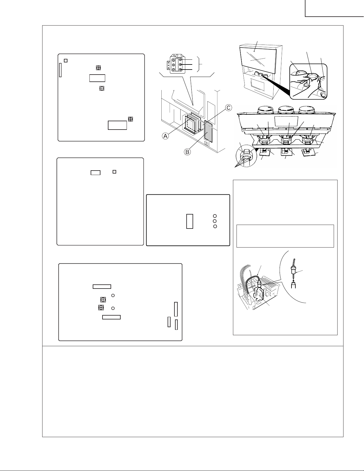
Assembly Adjustment Location and Items
A TUNER • µ-COM ASSY (A SIDE)
K2702
J2703
VR2701
916
IC2701
18
VR2801
FOCUS VR (VR1)
B
G FOCUS VR
R
Translucent paper such as tracing paper
Lens assy
(For Red)
64LHP5000
PROJECTOR UNIT
Lens assy
(For Green)
Lens assy
(For Blue)
52 27
IC2202
126
TUNER • µ-COM ASSY (B SIDE)
IC2702
14 8
71
Q2708
B POWER SUPPLY ASSY
IC207
91
VR201
VR202
TP201
TP204
91
IC201
L2202
C VIDEO ASSY (A SIDE)
IC5251
12856
15
1
1
1
11
10
P5252
29
P5254
Deflection
yoke (B)
CRT assy B
Deflection
yoke
B CRT DRIVE
Centering magnet
(Turn in either direction untill cross signal becomes white.)
assy
TP-BK
CRT assy G
G CRT DRIVE
assy
MEASURING METHOD
Disconnect the FBT anode cable as shown below.
Measure at the point where the cable enters the FBT.
Caution: Take extra precaution when measuring the
voltage. High voltage are also present in
surrounding circuit boards. (CRT DRIVE assy,
P5253
POWER SUPPLY assy).
SERVICEMAN W ARNING
Before removing the anode cable, turn off the power,
unplug the AC plug and let the unit discharge for more
than 1 minute.
Anode cable
FBT
Note:
When reconnecting the cable, proceed in the reverse
order. After reconnecting, tug on the cable to check
that it is secure.
TP-GK
Deflection
yoke (G)
CRT assy R
Pull straight up
Deflection
yoke (R)
R CRT DRIVE
assy
!Power supply adjustment
@Contrast coarse adjustment
#Brightness adjustment (PIONEER’s standard settings)
$Deflection yoke lean adjustment
%Screen center adjustment
^Focus adjustment of lens assy
&Focus VR adjustment
*Vertical size adjustment
(Horizontal size adjustment
)Convergence adjustment
QTest cross H-center position adjustment
WTuner block adjustment
EWhite balance adjustment
RPIONEER’s standard settings
TSide panel adjustment (Screen size 4:3)
YSPLIT screen adjustment
15
Page 16

64LHP5000
PROJECTOR UNIT
Ë
Assembly Adjustment Location Guide
If POWER SUPPLY ASSY
B
is repaired
1
Power supply adjustment
If DEFLECTION ASSY
If VIDEO ASSY
C
If TUNER µ-COM ASSY
A
If AMP ASSY
is repaired or replaced
is repaired or replaced
the µ-COM block
is repaired
(*1)
the tuner block
is repaired or replaced
is replaced
is replaced
No adjustment is required
7
Focus VR adjustment
8
Vertical size adjustment
9
Horizontal size adjustment
10
Convergence adjustment
13
White balance adjustment
3
Brightness adjustment
13
White balance adjustment
14
SHARP's standard settings
15
Side panel adjustment
2
Contrast coarse adjustment
3
Brightness adjustment
11
Test cross H-center position adjustment
14
SHARP's standard settings
12
Tuner block adjustment
All the above adjustments except for the test-cross H-center
11
position adjustment and tuner adjustment are required.
8
Vertical size adjustment
9
Horizontal size adjustment
10
Convergence adjustment
3
Brightness adjustment (SHARP's standard settings)
If R, G or B CRT DRIVE ASSY
If CRT ASSY
If LENS ASSY
is repaired or replaced
R, G, B or deflection yoke is replaced
is replaced
13
White balance adjustment
4
Deflection yoke lean adjustment
5
Screen center adjustment
7
Focus VR adjustment
10
Convergence adjustment
13
White balance adjustment
14
SHARP's standard settings
6
Focus adjustment of lens assy
10
Convergence adjustment
Check white balance. If the best screen is not obtained, adjust
If SIGNAL ASSY
If SUB VIDEO ASSY
If CONVER. DAC ASSY
If OTHER ASSY
is repaired or replaced
is repaired or replaced
is repaired or replaced
is repaired or replaced
13
White balance adjustment
16
SPLIT screen adjustment
13
White balance adjustment
14
SHARP's standard settings
10
Convergence adjustment
No adjustment is required
(*1) When replacing the tuner u-com assembly, mount the IC2204 (24LC32A:E2 PROM)on the current assembly to the new one to facilitate
adjustments.
16
Page 17

64LHP5000
PROJECTOR UNIT
Ë
Factory ADJ Mode
Select 1st FACTORY ADJ Mode
Start
“ON”
Front panel
Push the
switch with
thin rod.
Start
1st FAC
Selecting the mode for adjustment operations.
2
4
.................. Start adjusting
............ Select 1st factory adjustment mode, then adjust.
Normal
picture
Cyclically
2nd FACTORY ADJ
mode
picture
1
(MUTE) (MUTE)
STD OFFSET mode
(MUTE)
GENCE mode (ENTER)
(MUTE)
(∞ DOWN)
Telop : Blue
MANUAL CONVER-
Telop : White
AUTO ADJ mode
( LEFT)
Telop : White
1st FACTORY ADJ
mode
picture
RANGE CHECK mode
(MENU ON)
Telop : Red
The 2nd factory adjustment
mode is not used in the
adjustment.
PANEL ADJ mode
(FLASHBACK)
Telop : Yellow
(MUTE)
ADJUSTMENT SIZE
mode (ANT-A/B)
Telop : Green
(MUTE)
ADJUSTMENT MPX mode
(P IN P ON/OFF) (TWIN PICTURE)
Telop : Magenta
5
3
7
(MUTE)
Not used in the
adjustment
EPG CHECK mode
Note :
The brackets ( ) show the operation key.
TEST mode
( RIGHT)
Telop : Green
(GUIDE/TV)
Telop : Yellow
DTV PANEL mode
Telop : Yellow
(DTV)
SIGNAL ADJ mode
OTHERS OFFSET
(FF )
Telop : White
mode (XXXA)
Telop : -----
6
8
17
Page 18

64LHP5000
PROJECTOR UNIT
Adjustment Range Mode
1
Start
ADJUSTMENT
VOL 20
1st FAC
PD5462A RANGE
ADJUSTMENT
COLOR, BASS CNT
<VOLUME>
PD5462A RANGE
Telop : Red
: Vol 20
: Vol 30
: Vol 0
Picture quality, eyc., Change amount check made operating.
: COLOR,
BASS
: TINT,
TREBLE
: CONTRAST,
BALANCE
: BRIGHT
: SHARP-
NESS
: DETAIL
: S.V.M
TINT SHARPNESS
Center
CNT
The color to purple
MIN
The color to green
MAX
CNT
MIN
Cyclically
MAX
Center
Sharp
Soft
Adjustment OFFSET Mode
2
Start
1st FAC
STD
: STD OFFSET (NTSC)
: COMP (31kHz, 33kHz) OFFSET (HD)
: COMP (15kHz) OFFSET
(NTSC Component)
<Data value section>
COLOR
Telop : Blue
OFFSET
–24
Data value
This mode is to set the standard picture quality for a normal picture.
<Picture quality>
: COLOR (–64 to 63)
: TINT (–64 to 63)
: CONTRAST (–64 to 63)
: BRIGHT (–128 to 127)
: SHARPNESS (–128 to 127)
: DETAIL (–128 to 127)
: VM (–128 to 127)
: DRV-R (–64 to 63)
: DRV-B (–64 to 63)
: CUT-R (–128 to 127)
or
: CUT-G (–128 to 127)
18
: CUT-B (–128 to 127)
Page 19

3
64LHP5000
PROJECTOR UNIT
Size Mode
Start
1st FAC
<Size mode>
• Mode for roughly adjusting the horizontal and vertical sizes of the main deflection.
• In this mode, the color is green only, screen size is FULL and the contrast is
+10.
• The above settings are cleared when this mode is exited.
<Data value section>
ADJUSTMENT
H SIZE –24
Size mode
CH + : H PHA
or
(31 kHz)
CH – : H PHA
(33 kHz)
Telop : Green
: H Size
: V Size
: P HA
Screen mode
FULL SIZE
Data value
For
service
or
(–128 to 127)
Table on H SIZE and V SIZE data
Picture quality mode
NATURAL
ZOOM
CINEMA
FULL
FULL (MD)
A, B: are adjustment values.
D: Fixed value.
H SIZE
A
A
A
A
A+D
V SIZE
B
B
B
B
B
<View mode>
Table on H PHA data
: FULL (HD) H SIZE and
fixed value D can be
varied.
FULL ZOOM CINEMA WIDE
FULL (HD) NATURAL WIDE
PHA
Component input
(INPUT1, INPUT2)
DTV
(NTSC system)
15 kHz 31 kHz 33 kHz
CEFG C
C: Adjustment value
G: Fixed value
E, F: Fixed value + arbitrary service values
Others
19
Page 20

64LHP5000
PROJECTOR UNIT
4
Convergence Setting Mode
Start
1st FAC
<Variety section>
ADJUSTMENT
GV STATIC
Adjustment item
Variety
GV (Green, vertical)
GH (Green, horizontal)
BV (Blue, vertical)
Telop : White
Cyclically
Screen mode
FULL
–120
–128~127
Data value
RH (Red, horizontal)
RV (Red, vertical)
BH (Blue, horizontal)
<Data value section>
oror
ADJUSTMENT FULL
GV STATIC
–120
Data value
<Adjustment item section> <View mode>
STATIC (H, V)
SKEW 3D SKEW 5D SKEW
BOW 4D BOW 6D BOW
SUB KEY M S KEY 3S KEY
KEY MID KEY 3D KEY
SUB PIN M S PIN 4S PIN
PIN MID PIN 4D PIN
LIN MID LIN 6D LIN
SIZE MID SIZE 5D SIZE
M 3S KEY
M 3D KEY
M 4S PIN
M 4D PIN
<CRT control>
: Red ON/OFF
: Green ON/OFF
: Blue ON/OFF
FULL ZOOM CINEMA
WIDE
FULL (HD) NATURAL
WIDE
20
Page 21

5
Panel Adjustment Mode
64LHP5000
PROJECTOR UNIT
Start
1st FAC
• Mode for adjusting the brightness, width, and position of the gray part (panel) of
the 4:3 normal screen.
<Data value section>
ADJUSTMENT
Telop : Yellow
PANEL
–24
BRIGHT
Data value
<Adjustment item section>
6
DTV Panel Adjustment Mode (When option is mounted)
or
: BRIGHT (–64 to 63)
: CONTRAST (–64 to 63)
: WIDTH (–128 to 127)
: POSITION (–128 to 127)
Start
1st FAC
ADJUSTMENT
Telop : Yellow
DTV PANEL
–24
BRIGHT
Data value
• Mode for adjusting the brightness, width, and position of the gray part (panel) of
the 4:3 normal screen of the DTV tuner.
<Data value section>
or
<Adjustment item section>
: BRIGHT (–64 to 63)
: CONTRAST (–64 to 63)
: WIDTH (–128 to 127)
: POSITION (–128 to 127)
21
Page 22

64LHP5000
PROJECTOR UNIT
7
Adjustment MPX Mode
Start
1st FAC
For adjusting the TV tuner MPX decoder section
Auto adjust
(P IN P)
8
Others OFFSET Mode
Start
1st FAC
ADJUSTMENT
1 ATT
2 ST VCO
3 SAP VC
4 ST LPF
9
27
10
26
00001
MPX F.E 1
5 SAP LPF
6 WIDE BAN
7 SPECTRA
Telop : Magenta
Picture quality mode
MOVIE OFFSET
8
12
23
ADJUSTMENT
1 ATT
2 ST VCO
3 SAP VC
4 ST LPF
MPX F.E 1
9
5 SAP LPF
29
6 WIDE BAN
9
7 SPECTRA
30
00001
COMPLETE !
8
12
21
Yellow
“NG”
ADJUSTMENT
1 ATT
2 ST VCO
3 SAP VC
4 ST LPF
MPX F.E 1
9
5 SAP LPF
25
6 WIDE BAN
8
7 SPECTRA
30
00001
TRY AGAIN !!
8
12
23
Red
<Picture quality>
: COLOR (–64 to 63)
: TINT (–64 to 63)
–24
COLOR
Data value
OFFSET MODE
Direct Key Screen Display Picture quality mode
(Blue) MOVIE MOVIE OFFSET MODE
(Green) GAME GAME OFFSET MODE
(Red) TV TV OFFSET MODE
COLOR TEMP (STD) COLOR TEMP LOW for STD &
COLOR TEMP (MOVIE)
(GAME) OFFSET MODE
COLOR TEMP LOW for MOVIE
OFFSET MODE
: CONTRAST (–64 to 63)
: BRIGHT (–128 to 127)
: SHARPNESS (–128 to 127)
: DETAIL (–128 to 127)
: VM (–128 to 127)
: DRV-R (–64 to 63)
: DRV-B (–64 to 63)
: CUT-R (–128 to 127)
: CUT-G (–128 to 127)
: CUT-B (–128 to 127)
<Data value section>
or
22
Page 23

Ë
Adjustment
Power supply adjustment
1
-1
1
Start
64LHP5000
PROJECTOR UNIT
135V Power supply adjustment
Color-bar generator
D. DC voltmeter
Color bar
TP201
VR201
135.0V±1V
14.5V Power supply adjustment
-2
1
Start
Color bar
Contrast coarse adjustment
2
Start
1st FAC
POWER SUPPLY
ASSY
TP204
VR202
POWER SUPPLY
ASSY
VR201
Color-bar generator
D. DC voltmeter
14.5V ± 0.1V
VR202
ADJUSTMENT OFFSET
ADJUSTMENT OFFSET
COLOR
Telop : Blue
Data value
23
CONTRAST
or
Telop : 0
Page 24

64LHP5000
PROJECTOR UNIT
Brightness adjustment
3
Start
1st FAC
ADJUSTMENT OFFSET
CUTR
Telop : Blue
Data value
CUT-R
CUT-B
0
BRIGHT
or
Oscilloscope
or
G CRT DRIVE
assy
Cut of level
(180V DC)
TP-GK
GND
Deflection yoke lean adjustment
4
Start
Cross hatch
CRT assy B
Deflection
yoke
TP-GK
Deflection
yoke (G)
CRT assy R
R CRT DRIVE
assy
Deflection
yoke (R)
Deflection
yoke (B)
B CRT DRIVE assy
Centering magnet
(Turn in either direction untill cross signal becomes white.)
CRT assy G
TP-BK
G CRT DRIVE assy
24
Page 25

• For Red or Blue adjustment, turn 1st FACTORY ADJ mode ON
and then OFF to place the convergence POSITION at the center
of the adjustable range.
• Move the centering magnet of the deflection yoke for the
replaced color so that the horizontal and vertical lines at the
center of the screen align with the lines for a color not replaced.
Cross hatch
Screen center adjustment
5
Start
Focus adjustment of lens assy
6
Start
64LHP5000
PROJECTOR UNIT
Deflection yoke
Centering magnet
(Turn in either direction until cross signal becomes white.)
Translucent paper such as tracing paper
Focus VR adjustment
7
Start
Cross hatch
Cross hatch
FOCUS VR (VR1)
B
G FOCUS VR
R
“Best focusing”
Lens assy
(For Red)
Lens assy
(For Green)
Lens assy
(For Blue)
Turn the focus VR for best focusing.
25
Page 26
64LHP5000
PROJECTOR UNIT
Vertical size adjustment
8
Start
1st FAC
Monoscope
or
General
broadcasting
Green screen
V .SIZE
Adjust the size so that the picture is completely
displayed on the screen.
Note :
After the V. SIZE adjustment,
enter the H. SIZE adjustment by
pressing “1” key and readjust.
Screen mode : FULL
91% ± 2%
Note :
After the H. SIZE adjustment,
enter the V. SIZE adjustment by
pressing “2” key and readjust.
26
Page 27

Horizontal size adjustment
9
Start
1st FAC
Monoscope
64LHP5000
PROJECTOR UNIT
Note :
Screen mode : FULL
Green screen
H.SIZE
or
General
broadcasting
Adjust the size so that the picture is completely
displayed on the screen.
91% ± 2%
27
Page 28

64LHP5000
PROJECTOR UNIT
Convergence adjustment
10
10
Green line adjustment
-1
1st FAC
• Adjustment in the horizontal direction
Start
» Horizontal correction adjustment of the green line
• See 4 Convergence Setting Mode in the Factory ADJ mode.
• Input cross-hatch signals to this device’s video input terminal.
• The green line serves as the reference line in the adjustment of
red and blue. Perform this accurately.
Adjust the convergence of the green line using only green.
• Select the Adjustment item
GH - STATIC
or
In particular, be aware of the
setting before adjustment.
Adjustment Items
1
2
3
4
5
6
Center-line Adjustment
7
"
GH-STATIC
"
GH-SKEW
"
GH-BOW
"
(GH-3D SKEW)
"
(GH-4D BOW)
"
(GH-5D SKEW)
"
(GH-6D BOW)
Screen No.
1
2
5
3
6
4
7
• Adjust the center vertical line to the screen center position.
• Adjust so that the green vertical line at the center becomes a straight line with neither
Note: Do not adjust items 4 to 7.
• Adjust the Data value
distortion nor tilting.
Note :
The convergence for this device must be adjusted for each
screen size FULL (NTSC, 4:3 NORMAL), ZOOM (NTSC), CINEMA WIDE (NTSC), NATURAL WIDE (NTSC), FULL (HD)
(33.75 kHz, DTV).
RED
OFF
Green only
Note :
• Repeat the adjustments until you attain the
optimum state.
• Fine-adjust over the entire picture to obtain the
or
optimum picture.
• If the adjustment of H-STATIC is not possible
within the range of 010 to –010, set the data value
to 0, turn the centering magnet of the deflection
yoke and fine-adjust H-STATIC.
Adjustment Method
GREEN
ON
BLUE
OFF
1
2
3
4
5
6
Line-interval Adjustment
Ë
Screen
• STATIC
Key
No.
)
• SKEW
Key
No.
1
Key
No.
• BOW
2
"
GH-SIZE
"
GH-MID SIZE
"
GH-LIN
"
GH-MID LIN
"
(GH-5D SIZE)
"
(GH-6D LIN)
1
2
5
• 3D SKEW
• 4D BOW
8
9
A
B
0
C
• Adjust so that the intervals of the green vertical lines in the right and left sections of the
screen are symmetrical and correct.
Note: Do not adjust items 5 and 6.
» Screen’s changes in the horizontal direction when manual convergence
adjustment is mode
The changes at the arrow parts shown below are those implemented using
the Volume
key is used.
3
• 5D SKEW
4
Key
No.
± key. Changes are opposite to the arrow when the Volume —
= Fixed position
• SIZE
8
• MID SIZE
9
• 5D SIZE
8
6
• 6D BOW
7
Key
No.
• LIN
11
• MID LIN
12
7
Fig. 1. Horizontal correction (1)
• 6D LIN
10
13
28
Page 29

» Horizontal correction adjustment of the green line
• Select the Adjustment item
GH - SUB PIN
or
In particular, be aware of the
setting before adjustment.
• Adjust the Data value
Note :
• Repeat the adjustments until you attain the
optimum state.
• Fine-adjust over the entire picture to obtain the
or
optimum picture.
• If the adjustment of H-STATIC is not possible
within the range of 010 to –010, set the data value
to 0, turn the centering magnet of the deflection
yoke and fine-adjust H-STATIC.
64LHP5000
PROJECTOR UNIT
Adjustment Items
1
2
3
Lean Adjustment
4
1
2
3
4
5
6
7
8
Distortion Adjustment
9
10
11
12
*1 : Adjust taking note of the green vertical lines at 1/4 of the left and right sides of the screen.
"
GHKEY
"
GH-MID KEY
"
GH-SUB KEY
"
GH-M S KEY
"
GH-3D KEY
"
(GH-M 3D KEY)
"
GH-3DS KEY
"
(GH-M 3S KEY)
"
GH-PIN
"
GH-MID PIN
"
GH-SUB PIN
"
GH-M S PIN
"
GH-4D PIN
"
(GH-M 4D PIN)
"
GH-4DS PIN
"
(GH-M 4S PIN)
*1
*1
*1
*1
*1
*1
*1
*1
Screen No.
E
F
I
J
G
H
K
L
M
N
Q
R
O
P
S
T
• Adjust so that the vertical green lines on the left and right sides of the screen do not tilt.
• Adjust so that the vertical green lines on the left and right sides of the screen become
straight with no distortion.
Note: Do not adjust items 2, 4, 10 and 12.
Adjustment Method
Ë
Key
No.
4
Key
No.
3
Key
No.
6
Key
No.
5
Screen
• SUB KEY
• SUB PIN
• KEY
• PIN
15
19
23
27
• MID KEY
• M S KEY
• MID PIN
• M S PIN
16
20
24
28
Fig. 2. Horizontal correction (2)
• 3D KEY
• 3DS KEY
• 4D PIN
• 4DS PIN
17
21
25
29
29
• M 3D KEY
• M 3S KEY
• M 4D PIN
• M 4S PIN
» Screen’s changes in the horizontal direction when
18
manual convergence adjustment is mode
The changes at the arrow parts shown below are those
implemented using the Volume
opposite to the arrow when the Volume
± key. Changes are
— key is used.
22
26
30
= Fixed position
Page 30

64LHP5000
PROJECTOR UNIT
10
Green line adjustment
-2
1st FAC
• Adjustment in the vertical direction
Start
» Vertical correction adjustment of the green line
• Select the Adjustment item
GV - STATIC
or
In particular, be aware of the
setting before adjustment.
Adjustment Items
1
2
3
4
5
6
Center-line Adjustment
7
"
GV-STATIC
"
GV-SKEW
"
GV-BOW
"
(GV-3D SKEW)
"
(GV-4D BOW)
"
(GV-5D SKEW)
"
(GV-6D BOW)
Screen No.
1
2
5
3
6
4
7
• Adjust the center horizontal line to the center of the screen.
• Adjust so that the green vertical line at the center becomes a straight line with neither
Note: Do not adjust items 6 and 7.
• Adjust the Data value
distortion nor tilting.
Note :
• Repeat the adjustments until you attain the
optimum state.
• Fine-adjust over the entire picture to obtain the
or
optimum picture.
• If the adjustment of V-STATIC is not possible
within the range of 010 to –010, set the data value
to 0, turn the centering magnet of the deflection
yoke and fine-adjust V-STATIC.
Adjustment Method
1
2
3
4
5
6
Line-interval Adjustment
Ë
Screen
• STATIC
Key
No.
)
• SKEW
Key
No.
1
Key
No.
• BOW
2
"
GV-SIZE
"
GV-LIN
"
GV-MID SIZE
"
GV-MID LIN
"
(GV-5D SIZE)
"
(GV-6D LIN)
1
2
5
• 3D SKEW
• 4D BOW
8
A
9
B
0
C
• Adjust so that the intervals of the green horizontal lines at the top and bottom of the
screen are symmetrical and correct.
Note: Do not adjust items 5 and 6.
» Screen’s changes in the vertical direction when manual convergence
adjustment is mode
The changes at the arrow parts shown below are those implemented using
the Volume
key is used.
3
• 5D SKEW
4
± key. Changes are opposite to the arrow when the Volume —
• SIZE
8
• MID SIZE
9
• 5D SIZE
Key
No.
8
6
• 6D BOW
7
• LIN
11
• MID LIN
12
• 6D LIN
Key
No.
7
10
13
= Fixed position
Fig. 3. Vertical correction (1)
30
Page 31

» Vertical correction adjustment of the green line
• Select the Adjustment item
GV - SUB PIN
or
In particular, be aware of the
setting before adjustment.
• Adjust the Data value
Note :
• Repeat the adjustments until you attain the
optimum state.
• Fine-adjust over the entire picture to obtain the
or
optimum picture.
• If the adjustment of V-STATIC is not possible
within the range of 010 to –010, set the data value
to 0, turn the centering magnet of the deflection
yoke and fine-adjust V-STATIC.
64LHP5000
PROJECTOR UNIT
Adjustment Items
"
1
2
3
Lean Adjustment
4
1
2
3
4
5
6
7
8
9
Distortion Adjustment
10
11
12
*2 : Adjust taking note of the green horizontal lines at 1/4 of the left and right sides of the screen.
GV-KEY
"
GV-MID KEY
"
GV-SUB KEY
"
GV-M S KEY
"
GV-3D KEY
"
(GV-M 3D KEY)
"
GV-3DS KEY
"
(GV-M 3S KEY)
"
GV-PIN
"
GV-MID PIN
"
GV-4D PIN
"
(GV-M 4D PIN)
"
GV-SUB PIN
"
GV-M S PIN
"
GV-4DS PIN
"
(GV-M 4S PIN)
*2
*2
*2
*2
*2
*2
*2
*2
Screen No.
E
F
I
J
G
H
K
L
M
N
O
P
Q
R
S
T
• Adjust so that the green horizontal lines at the top and bottom of the screen do not tilt.
• Adjust so that the green horizontal lines at the top and bottom of the screen become
straight with no distortion.
Note: Do not adjust items 2, 4, 8 and 12.
Adjustment Method
Ë
Key
No.
4
Key
No.
3
Key
No.
6
Key
No.
5
Screen
• SUB KEY
• SUB PIN
• KEY
• PIN
15
19
23
27
• MID KEY
• M S KEY
• MID PIN
• M S PIN
16
20
24
28
Fig. 4. Vartical correction (2)
• 3D KEY
• 3DS KEY
• 4D PIN
• 4DS PIN
17
21
25
29
31
• M 3D KEY
• M 3S KEY
• M 4D PIN
• M 4S PIN
» Screen’s changes in the vertical direction when
18
manual convergence adjustment is mode
The changes at the arrow parts shown below are those
implemented using the Volume
opposite to the arrow when the Volume
± key. Changes are
— key is used.
22
26
30
= Fixed position
Page 32

64LHP5000
PROJECTOR UNIT
10
Red line adjustment
-3
1st FAC
• Adjustment in the horizontal direction
Start
» Horizontal correction adjustment of the red line
• See 4 Convergence Setting Mode in the Factory ADJ mode.
• Input cross-hatch signals to this device’s video input terminal.
• Adjust the convergence of the red line using the green and red
lines.
• Select the Adjustment item
• Adjust the Data value
RH - STATIC
or
In particular, be aware of the
setting before adjustment.
Adjustment Item
1
2
3
4
5
6
Center-line Adjustment
7
RH-STATIC
RH-SKEW
RH-BOW
(RH-3D SKEW)
(RH-4D BOW)
(RH-5D SKEW)
(RH-6D BOW)
"
"
"
"
"
"
"
Screen No.
1
2
5
3
6
4
7
• Adjust the red center to match the green center.
• Overlap the red vertical line at the center with the green vertical line.
Note: Do not adjust items 6 and 7.
RED
ON
RED + GREEN
Note :
• Ov erlap the green line with the red line, so that the line
becomes yellow .
• Repeat the adjustments until you attain the optimum
state.
or
• Fine-adjust ov er the entire picture to obtain the optimum
picture.
• If the adjustment is of H-STATICnot possible within the
range of 010 to –010, set the data value to 0, turn the
centering magnet of the deflection yoke and fine-adjust
H-STATIC.
Adjustment Method
GREEN
ON
BLUE
ON
1
2
3
4
5
6
Line-interval Adjustment
Ë
Screen
• STATIC
Key
No.
)
• SKEW
Key
No.
1
Key
No.
• BOW
2
"
RH-SIZE
"
RH-LIN
"
RH-MID SIZE
"
RH-MID LIN
"
(RH-5D SIZE)
"
(RH-6D LIN)
1
2
5
• 3D SKEW
• 4D BOW
8
A
9
B
0
C
• Adjust the interval at the center of the red vertical line to the interval of the green vertical
line.
Note: Do not adjust items 5 and 6.
» Screen’s changes in the horizontal direction when manual convergence
adjustment is mode
The changes at the arrow parts shown below are those implemented using
the Volume
key is used.
3
• 5D SKEW
4
Key
No.
± key. Changes are opposite to the arrow when the Volume —
= Fixed position
• SIZE
8
• MID SIZE
9
8
6
• 6D BOW
7
Key
No.
• LIN
11
• MID LIN
12
7
Fig. 5. Horizontal correction (1)
• 5D SIZE
• 6D LIN
10
13
32
Page 33

» Horizontal correction adjustment of the red line
• Select the Adjustment item
RH - SUB PIN
or
In particular, be aware of the
setting before adjustment.
• Adjust the Data value
Note :
• Repeat the adjustments until you attain the
optimum state.
• Fine-adjust over the entire picture to obtain the
or
optimum picture.
• If the adjustment of H-STATIC is not possible
within the range of 010 to –010, set the data value
to 0, turn the centering magnet of the deflection
yoke and fine-adjust H-STATIC.
64LHP5000
PROJECTOR UNIT
Adjustment Item
1
2
3
Lean Adjustment
4
1
2
3
4
5
6
7
8
9
Distortion Adjustment
10
11
12
*3 : Adjust taking note of the red horizontal lines at 1/4 of the left and right sides of the screen.
Ë
Screen
"
RH-KEY
"
RH-MID KEY
"
RH-SUB KEY
"
RH-M S KEY
"
RH-3D KEY
"
(RH-M 3D KEY)
"
RH-3DS KEY
"
(RH-M 3S KEY)
"
RH-PIN
"
RH-MID PIN
"
RH-4D PIN
"
(RH-M 4D PIN)
"
RH-SUB PIN
"
RH-M S PIN
"
(RH-4DS PIN)
"
RH-M 4S PIN
• KEY
*3
*3
*3
*3
15
*3
*3
*3
*3
• MID KEY
Screen No.
E
F
I
J
G
H
K
L
M
N
O
P
Q
R
S
T
16
• Adjust so that the red vertical lines at the top and bottom of the screen do not tilt.
• Adjust so that the red vertical line at the top and bottom of the screen overlap with the
green vertical lines, and becomes a straight line with no distortion.
Note: Do not adjust items 2, 4, 8 and 11.
17
• 3D KEY
• M 3D KEY
Key
No.
4
Adjustment Method
» Screen’s changes in the horizontal direction when
18
manual convergence adjustment is mode
The changes at the arrow parts shown below are those
implemented using the Volume
opposite to the arrow when the Volume
± key. Changes are
— key is used.
Key
No.
3
Key
No.
6
Key
No.
5
• SUB KEY
• PIN
• SUB PIN
19
23
27
• M S KEY
• MID PIN
• M S PIN
20
24
28
Fig. 6. Horizontal correction (2)
• 3DS KEY
• 4D PIN
• 4DS PIN
21
25
29
33
• M 3S KEY
• M 4D PIN
• M 4S PIN
22
26
30
= Fixed position
Page 34

64LHP5000
PROJECTOR UNIT
10
Red line adjustment
-4
1st FAC
• Adjustment in the vertical direction
Start
» Vertical correction adjustment of the red line
• Select the Adjustment item
RV - STATIC
or
In particular, be aware of the
setting before adjustment.
Adjustment Item
1
2
3
4
5
6
Center-line Adjustment
7
RV-STATIC
RV-SKEW
RV-BOW
RV-3D SKEW
RV-4D BOW
(RV-5D SKEW)
(RV-6D BOW)
"
"
"
"
"
"
"
Screen No.
1
2
5
3
6
4
7
• Adjust the red center to match the green center.
• Adjust so that the red horizontal line at the center overlaps with the green horizontal
line.
Note: Do not adjust items 6 to 7.
• Adjust the Data value
Note :
• Repeat the adjustments until you attain the
optimum state.
• Fine-adjust over the entire picture to obtain the
or
optimum picture.
• If the adjustment of V-STATIC is not possible
within the range of 010 to –010, set the data value
to 0, turn the centering magnet of the deflection
yoke and fine-adjust V-STATIC.
Adjustment Method
1
2
3
4
5
6
Line-interval Adjustment
Ë
Screen
• STATIC
Key
No.
)
• SKEW
Key
No.
1
Key
No.
• BOW
2
"
RV-SIZE
"
RV-LIN
"
RV-MID SIZE
"
RV-MID LIN
"
(RV-5D SKEW)
"
(RV-6D LIN)
1
2
5
• 3D SKEW
• 4D BOW
8
A
9
B
0
C
• Adjust the interval at the center of the red vertical line to the interval of the green vertical
line.
Note: Do not adjust items 5 and 6.
» Screen’s changes in the vertical direction when manual convergence
adjustment is mode
The changes at the arrow parts shown below are those implemented using
the Volume
key is used.
3
• 5D SKEW
4
± key. Changes are opposite to the arrow when the Volume —
• SIZE
8
• MID SIZE
9
Key
No.
8
6
• 6D BOW
7
• LIN
11
• MID LIN
12
Key
No.
7
• 5D SIZE
• 6D LIN
10
13
= Fixed position
Fig. 7. Vertical correction (1)
34
Page 35

» Vertical correction adjustment of the red line
• Select the Adjustment item
RV - SUB PIN
or
In particular, be aware of the
setting before adjustment.
• Adjust the Data value
Note :
• Repeat the adjustments until you attain the
optimum state.
• Fine-adjust over the entire picture to obtain the
or
optimum picture.
• If the adjustment of V-STATIC is not possible
within the range of 010 to –010, set the data value
to 0, turn the centering magnet of the deflection
yoke and fine-adjust V-STATIC.
64LHP5000
PROJECTOR UNIT
Adjustment Item
1
2
3
4
"
RV-KEY
"
RV-MID KEY
"
RV-SUB KEY
"
RV-M S KEY
*4
*4
Lean Adjustment
1
2
3
4
5
6
7
8
9
Distortion Adjustment
10
11
12
*4 : Adjust taking note of the red horizontal lines at 1/4 of the left and right sides of the screen.
"
RV-3D KEY
"
(RV-M 3D KEY)
"
RV-3DS KEY
"
(RV-M 3S KEY)
"
RV-PIN
"
RV-MID PIN
"
RV-4D PIN
"
(RV-M 4D PIN)
"
RV-SUB PIN
"
RV-M S PIN
"
RV-4DS PIN
"
(RV-M 4S PIN)
*4
*4
*4
*4
*4
*4
Screen No.
E
F
I
J
G
H
K
L
M
N
O
P
Q
R
S
T
• Adjust so that the red horizontal lines at the left and right of the screen do not tilt.
• Adjust so that the red horizontal lines at the left and right of the screen overlap with the
green horizontal lines, and become a straight line with no distortion.
Note: Do not adjust items 2, 4, 8 and 12.
Adjustment Method
Ë
Key
No.
4
Key
No.
3
Key
No.
6
Key
No.
5
Screen
• SUB KEY
• SUB PIN
• KEY
• PIN
15
19
23
27
• MID KEY
• M S KEY
• MID PIN
• M S PIN
16
20
24
28
Fig. 8. Vartical correction (2)
• 3D KEY
• 3DS KEY
• 4D PIN
• 4DS PIN
17
21
25
29
35
• M 3D KEY
• M 3S KEY
• M 4D PIN
• M 4S PIN
» Screen’s changes in the vertical direction when
18
manual convergence adjustment is mode
The changes at the arrow parts shown below are those
implemented using the Volume
opposite to the arrow when the Volume
± key. Changes are
— key is used.
22
26
30
= Fixed position
Page 36

64LHP5000
PROJECTOR UNIT
10
Blue line adjustment
-5
1st FAC
• Adjustment in the horizontal direction
Start
» Horizontal correction adjustment of the blue line
• See 4 Convergence Setting Mode in the Factory ADJ mode.
• Input cross-hatch signals to this device’s video input terminal.
• Select the Adjustment item
BH - STATIC
or
In particular, be aware of the
setting before adjustment.
Adjustment Item
1
2
3
4
1
6
Center-line Adjustment
7
"
BH-STATIC
"
BH-SKEW
"
BH-BOW
"
BH-3D SKEW
"
BH-4D BOW
"
BH-5D SKEW
"
BH-6D BOW
Screen No.
1
2
5
3
6
4
7
• Adjust the blue center to match the green center.
• Overlap the blue vertical line at the center with the green vertical line.
Note: Do not adjust items 6 and 7.
• Adjust the Data value
RED
OFF
GREEN + BLUE
Note :
• Repeat the adjustments until you attain the
optimum state.
• Fine-adjust over the entire picture to obtain the
or
optimum picture.
• If the adjustment of H-STATIC is not possible
within the range of 010 to –010, set the data value
to 0, turn the centering magnet of the deflection
yoke and fine-adjust H-STATIC.
Adjustment Method
GREEN
ON
BLUE
ON
1
2
3
4
5
6
Line-interval Adjustment
Ë
Screen
• STATIC
Key
No.
)
• SKEW
Key
No.
1
Key
No.
• BOW
2
"
BH-SIZE
"
BH-LIN
"
BH-MID SIZE
"
BH-MID LIN
"
(BH-5D SIZE)
"
(BH-6D LIN)
1
2
5
• 3D SKEW
• 4D BOW
8
A
9
B
0
C
• Adjust the interval at the center of the blue vertical line to the interval of the green
vertical line.
Note: Do not adjust items 5 and 6.
» Screen’s changes in the horizontal direction when manual convergence
adjustment is mode
The changes at the arrow parts shown below are those implemented using
the Volume
key is used.
3
• 5D SKEW
4
Key
No.
± key. Changes are opposite to the arrow when the Volume —
= Fixed position
• SIZE
8
• MID SIZE
9
• 5D SIZE
8
6
• 6D BOW
7
Key
No.
• LIN
11
• MID LIN
12
7
Fig. 9. Horizontal correction (1)
• 6D LIN
10
13
36
Page 37

» Horizontal correction and adjustment of blue line
• Select the Adjustment item
BH - SUB PIN
or
In particular, be aware of the
setting before adjustment.
• Adjust the Data value
Note :
• Repeat the adjustments until you attain the
optimum state.
• Fine-adjust over the entire picture to obtain the
or
optimum picture.
• If the adjustment of H-STATIC is not possible
within the range of 010 to –010, set the data value
to 0, turn the centering magnet of the deflection
yoke and fine-adjust H-STATIC.
64LHP5000
PROJECTOR UNIT
Adjustment Item
1
2
3
Lean Adjustment
4
1
2
3
4
5
6
7
8
9
Distortion Adjustment
10
11
12
*5 : Adjust taking note of the blue vertical lines at 1/4 of the left and right sides of the screen.
Ë
Screen
"
BH-KEY
"
BH-MID KEY
"
BH-SUB KEY
"
BH-M S KEY
"
BH-3D KEY
"
(BH-M 3D KEY)
"
BH-3DS KEY
"
(BH-M 3S KEY)
"
BH-PIN
"
BH-MID PIN
"
BH-4D PIN
"
(BH-M 4D PIN)
"
BH-SUB PIN
"
BH-M S PIN
"
BH-4DS PIN
"
(BH-M 4S PIN)
• KEY
*5
*5
*5
*5
15
*5
*5
*5
*5
• MID KEY
Screen No.
E
F
I
J
G
H
K
L
M
N
O
P
Q
R
S
T
16
• Adjust so that the blue vertical lines at the top and bottom of the screen do not tilt.
• Adjust so that the blue vertical lines at the top and bottom of the screen overlap with the
green vertical lines, and become a straight line with no distortion.
Note:Do not adjust items 2, 4, 8 and 12.
17
• 3D KEY
• M 3D KEY
Key
No.
4
Adjustment Method
» Screen’s changes in the horizontal direction when
18
manual convergence adjustment is mode
The changes at the arrow parts shown below are those
implemented using the Volume
opposite to the arrow when the Volume
± key. Changes are
— key is used.
Key
No.
3
Key
No.
6
Key
No.
5
• SUB KEY
• PIN
• SUB PIN
19
23
27
• M S KEY
• MID PIN
• M S PIN
20
24
28
• 3DS KEY
• 4DS PIN
Fig. 10. Horizontal correction (2)
• 4D PIN
21
25
29
37
• M 3S KEY
• M 4D PIN
• M 4S PIN
22
26
30
= Fixed position
Page 38

64LHP5000
PROJECTOR UNIT
10
Blue line adjustment
-6
1st FAC
• Adjustment in the vertical direction
Start
» Vertical correction adjustment of the blue line
• Select the Adjustment item
BV - STATIC
or
In particular, be aware of the
setting before adjustment.
Adjustment Item
1
2
3
4
5
6
Center-line Adjustment
7
BV-STATIC
BV-SKEW
BV-BOW
BV-3D SKEW
BV-4D BOW
BV-5D SKEW
BV-6D BOW
"
"
"
"
"
"
"
Screen No.
1
2
5
3
6
4
7
• Adjust the blue center to match the green center.
• Adjust so that the blue horizontal line at the center overlaps with the green horizontal
line.
• Adjust the Data value
Note :
• Repeat the adjustments until you attain the
optimum state.
• Fine-adjust over the entire picture to obtain the
or
optimum picture.
• If the adjustment of V-STATIC is not possible
within the range of 010 to –010, set the data value
to 0, turn the centering magnet of the deflection
yoke and fine-adjust V-STATIC.
Adjustment Method
1
2
3
4
5
6
Line-interval Adjustment
Ë
Screen
• STATIC
Key
No.
)
• SKEW
Key
No.
1
Key
No.
• BOW
2
"
BV-SIZE
"
BV-LIN
"
BV-MID SIZE
"
BV-MID LIN
"
(BV-5D SIZE)
"
(BV-6D LIN)
1
2
5
• 3D SKEW
• 4D BOW
8
A
9
B
0
C
• Adjust the interval at the center of the blue horizontal line to the interval of the green
horizontal line.
Note: Do not adjust items 5 and 6.
» Screen’s changes in the vertical direction when manual convergence
adjustment is mode
The changes at the arrow parts shown below are those implemented using
the Volume
key is used.
3
• 5D SKEW
4
± key. Changes are opposite to the arrow when the Volume —
• SIZE
8
• MID SIZE
9
Key
No.
8
6
• 6D BOW
7
• LIN
11
• MID LIN
12
Key
No.
7
• 5D SIZE
• 6D LIN
10
13
= Fixed position
Fig. 11. Vertical correction (1)
38
Page 39

» Vertical correction adjustment of the blue line
• Select the Adjustment item
BV - SUB PIN
or
In particular, be aware of the
setting before adjustment.
• Adjust the Data value
Note :
• Repeat the adjustments until you attain the
optimum state.
• Fine-adjust over the entire picture to obtain the
or
optimum picture.
• If the adjustment of V-STAC is not possible within
the range of 010 to –010, set the data value to 0,
turn the centering magnet of the deflection yoke
and fine-adjust V-STATIC.
64LHP5000
PROJECTOR UNIT
Adjustment Item
1
2
3
Lean Adjustment
4
1
2
3
4
5
6
7
8
9
Distortion Adjustment
10
11
12
*6 : Adjust taking note of the blue horizontal lines at 1/4 of the left and right sides of the screen
Ë
Screen
"
BV-KEY
"
BV-MID KEY
"
BV-SUB KEY
"
BV-M S KEY
"
BV-3D KEY
"
(BV-M 3D KEY)
"
BV-3DS KEY
"
(BV-M 3S KEY)
"
BV-PIN
"
BV-MID PIN
"
BV-4D PIN
"
(BV-M 4D PIN)
"
BV-SUB PIN
"
BV-M S PIN
"
BV-4DS PIN
"
(BV-M 4S PIN)
• KEY
*6
*6
*6
*6
15
*6
*6
*6
*6
• MID KEY
Screen No.
E
F
I
J
G
H
K
L
M
N
O
P
Q
R
S
T
16
• Adjust so that the blue horizontal lines at the left and right of the screen do not tilt.
• Adjust so that the blue horizontal lines at the left and right of the screen overlap with the
green horizontal lines, and become straight lines with no distortion.
Note: Do not adjust items 2, 4, 8 and 12.
17
• 3D KEY
• M 3D KEY
Key
No.
4
Adjustment Method
» Screen’s changes in the vertical direction when
18
manual convergence adjustment is mode
The changes at the arrow parts shown below are those
implemented using the Volume
opposite to the arrow when the Volume
± key. Changes are
— key is used.
Key
No.
3
Key
No.
6
Key
No.
5
• SUB KEY
• PIN
• SUB PIN
19
23
27
• M S KEY
• MID PIN
• M S PIN
20
24
28
Fig. 12. Vartical correction (2)
• 3DS KEY
• 4D PIN
• 4DS PIN
21
25
29
39
• M 3S KEY
• M 4D PIN
• M 4S PIN
22
26
30
= Fixed position
Page 40

64LHP5000
PROJECTOR UNIT
Test cross H-center position adjustment
11
Start
(LD player)
: ADJ CONVERGE
TUNER µ-COM
ASSY
Tuner block adjustment
12
Video level adjustment 1
-1
12
Start
L2202
TV SET UP
CONVERGENCE
SAT CONTROL
SYSTEM MODE
SPEAKER
EXIT
MONITOR OUT terminal
(75Ω treminal)
: OFF
: OFF
: INTERNAL
Adjust the position so that the
test cross is placed at the center
of the screen.
L2202
Dual trace oscilloscope
ANT A
RF signal :
fV = EIA color bar or white
100%, 60dBµV
9 ch (fp = 187.25MHz)
TUNER µ-COM
ASSY
VR2701
2Vp-p ± 0.2V
VR2701
40
Page 41

12
Video level adjustment 2
-2
Start
(P IN P)
P IN P ANT.A CH9
ON/OFF
INPUT
CH
SHIFT
EXIT
CH9
J2703 4 pin
VR2801
64LHP5000
PROJECTOR UNIT
Double screen
or
not 75Ω terminal
1Vp-p ± 0.10V
12
-3
Start
Stereo VCO adjustment
1st FAC
5. SAP UF 8
1. ATT 9
6.
2. ST VCO 29
3. SAP VC 9
4. STUF 30
TUNER µ-COM
ASSY
Q2708
00000
WIDE BAN
SPECTRA
7.
12
2
TUNER µ-COM
ASSY
Audio Rch output
(P IN P)
ST VCO adjustment
mode
VR2801
Frequency counter
or
62.936kHz
TV screen
1 ATT
2 ST VCO 31
3 SAP VC 8
4 ST LPF 31
or
5 SAP LPF 8
6 WIDE BAN 31
7 SPECTRA 31
41
Page 42

64LHP5000
PROJECTOR UNIT
SAP VCO adjustment
-4
12
Start
1. ATT 9
2. ST VCO 29
3. SAP VC 9
4. STUF 30
5. SAP UF 8
6.
WIDE BAN
SPECTRA
7.
00000
1st FAC
12
2
TUNER µ-COM ASSY
Q2708
K2702
(TP-MPX)
00001
11 01
78.67kHz
147mVrms
00
Oscillator
(P IN P)
1. ATT 9
2. ST VCO 29
3. SAP VC 9
4. STUF 30
or
5. SAP UF 8
WIDE BAN
6.
7.
SPECTRA
00001
12
2
If “TRY AGAIN” is
displayed, adjust
again as follows.
“COMPLETE”
Set to center
1. ATT 9
2. ST VCO 29
3. SAP VC 9
4. STUF 30
5. SAP UF 8
6.
WIDE BAN
SPECTRA
7.
00001
12
2
42
Page 43

12
STEREO LPF adjustment
-5
Start
1st FAC
TUNER µ-COM ASSY
Q2708
K2702
(TP-MPX)
9.4kHz
600mVrms
Sine wave
Oscillator
(P IN P)
ADJUSTMENT MPX
1. ATT 9
2. ST VCO 29
3. SAP VC 9
4. ST LPF 30
00000
5. SAP LPF 8
6.
WIDE BAN
SPECTRA
7.
64LHP5000
PROJECTOR UNIT
12
21
“COMPLETE”
12
SAP LPF adjustment
-6
Start
1st FAC
TUNER µ-COM ASSY
Q2708
01000
01
Set to center
K2702
(TP-MPX)
0
88kHz
120mVrms
Sine wave
Oscillator
or
ADJUSTMENT MPX
1. ATT 9
2. ST VCO 29
3. SAP VC 9
4. ST LPF 30
00000
ADJUSTMENT MPX
1. ATT 9
2. ST VCO 29
3. SAP VC 9
4. ST LPF 30
5. SAP LPF 8
6.
WIDE BAN
7.
SPECTRA
5. SAP LPF 8
WIDE BAN
6.
7.
SPECTRA
00000
If “TRY AGAIN” is
displayed, adjust
again as follows.
12
21
12
21
“COMPLETE”
00100
01
Set to center
(P IN P)
If “TRY AGAIN” is
or
displayed, adjust
again as follows.
0
ADJUSTMENT MPX
1. ATT 9
2. ST VCO 29
3. SAP VC 9
4. ST LPF 30
5. SAP LPF 8
6.
WIDE BAN
SPECTRA
7.
00000
12
21
43
Page 44

64LHP5000
PROJECTOR UNIT
Separation adjustment (WIDE BAND)
-7
12
12
Start
-8
Start
1st FAC
5. SAP UF 8
1. ATT 9
6.
2. ST VCO 29
3. SAP VC 9
4. STUF 30
WIDE BAN
7. SPECTRA 2
00000
Separation adjustment (SPECTRAL)
1st FAC
5. SAP UF 8
1. ATT 9
6.
2. ST VCO 29
3. SAP VC 9
4. STUF 30
WIDE BAN
7. SPECTRA 2
00000
12
12
ANT A
ANT A
Adjust the output of the TV OUT terminal on
the rear panel to the minimum level.
R ch level - L ch input (RF) minimum
or
L ch level - R ch input (RF) minimum
RF signal
Video signal : fV = EIA color-bar, 60dBµV
Audio signal : fA = 300Hz, 30% MOD, L ch
(or R ch) only, 54dBµV
9 ch (fp = 187.25MHz)
Adjust the output of the TV OUT terminal on
the rear panel to the minimum level.
R ch level - L ch input (RF) minimum
or
L ch level - R ch input (RF) minimum
RF signal
Video signal : fV = EIA color-bar, 60dBµV
Audio signal : fA = 3kHz, 30% MOD, L ch
(or R ch) only, 54dBµV
9 ch (fp = 187.25MHz)
»
Connection diagram for adjusting the tuner section:
Frequency
counter
DC
voltmeter
Waveform
monitor or
oscilloscope
Signal
generator
Test signal generator for adjustment
To each TP terminals of
the TUNER • µ-COM ASSY
PROJECTION MONITOR
RECEIVER
ANTENNA
MONITOR OUT
(Video)
MONITOR OUT
(Audio)
High frequency
attenuator
Oscilloscope
L.P.F.
L.P.F. : 100Hz - 10kHz : dB
15.75kHz - 100kHz : less than –40dB
Up
converter
OUT
Distortion
meter
+0
–0.5
2 signal pad
25Ω
25Ω
25Ω
Oscilloscope
IN
IF
modulator
IN
FM signal
generator
Note :
• Repeat step B -7 and B -8 till the best separation.
• When performing the separation adjustment, be sure to perform WIDE BAND adjustment first.
• If performing the WIDE BAND adjustment, be sure to perf orm SPECTRAL adjustment.
TV signal
generator
TV MPX signal
generator
Low frequency
oscillator
44
Page 45

White balance adjustment
13
64LHP5000
PROJECTOR UNIT
Start
Color bar signal
without color
signal
SHARP’s standard settings
14
1st FAC
STD OFFSET
COMP (31.33kHz) OFFSET
COMP (15kHz) OFFSET
Adjust the DRV-R and DRV-B
so that the bright part of the
screen becomes white.
Adjust the CUT-R and CUT -B
so that the dark part of the
screen become gray. (Don't
move the screen VR and CUT-G).
COLOR TEMP (STD)
COLOR TEMP (MOVIE)
: DRV-R
: DRV-B
: CUT-R
or
: CUT-B
14
14
Sharpness adjustment
-1
Start
-2
Start
1st FAC
Telop : Blue
Color adjustment
1st FAC
STD OFFSET
OFFSET
“Color bar”
OFFSET
“Multiburst”
P5253
VIDEO ASSY
Adjust the screen to optimum condition.
A : B = 5 : 6.6
A
Oscilloscope
B
1.25MHz
500kHz
45
Page 46

64LHP5000
PROJECTOR UNIT
Tint adjustment
-3
14
14
Start
-4
Start
1st FAC
Contrast adjustment
1st FAC
ADJUSTMENT
TINT
“Color bar”
OFFSET
Adjust the screen to optimum condition.
“Color bar”
ADJUSTMENT
CONTR
“Normal video signal”
OFFSET
Adjust the screen to optimum condition.
At the TP-BK of the B. CRT DRIVE assy, check that the
signal is shaped as shown below.
Saturated
Shapely waveform Shapeless waveform
46
Page 47

Side panel adjustment (Screen size 4 : 3)
15
Panel position adjustment
-1
15
64LHP5000
PROJECTOR UNIT
Start
1st FAC
(ADJUSTMENT PANEL MODE)
“Monoscope”
ADJUSTMENT
Telop : Yellow
91%
91%
“Monoscope”
Screen mode 4 : 3
• Set the information amount
for the right side of the
screen to 91%.
VR5252 (PANEL POSI)
PANEL
POSITION
Data value
or
–24
<Panel position data value>
or
91%
<Panel width data value>
or
91%
• Set the information amount for
the left side of screen to 91%.
VR5251 (PANEL WITH)
Ë
When the optional DTV tuner is
mounted
Start
(DTV PANEL ADJ MODE)
1st FAC
• Using the VOL+ and VOL– keys, adjust the information amount
at the right side of the screen to the same position as that when
NTSC signals are input.
• Using the VOL+ and VOL– keys, adjust the information amount
at the left side of the screen to the same position as that when
NTSC signals are input.
47
Page 48

64LHP5000
PROJECTOR UNIT
Adjustment of panel luminance
-2
15
Start
1st FAC
(ADJUSTMENT PANEL MODE)
“Monoscope”
Telop : Yellow
Screen mode 4 : 3
• When Panel Bright :
Black burst
• When Panel Contrast :
100% white
TP-G.K (PI5151)
G CRT DRIVE ASSY
PANELADJUSTMENT
BRIGHT
Data value
–24
<Panel contrast>
<Data value ><Panel bright>
or
Adjust the TP-G.K panel
level to 160V.
Panel Contrast
or
Adjustment
Ë
When the optional DTV tuner is
mounted
Start
(DTV PANEL ADJ MODE)
HD SG
Black burst
1st FAC
Screen mode 4 : 3
Adjust the TP-G.K panel level to the same
potential as Panel Bright Adjustment.
Panel level
Approx. 160VDC
Oscilloscope
+220V
+190V
GND
HD SG
White 100%
48
Page 49

SPLIT screen adjustment
“Color bar”
Double screen
• Adjust the left and right
screens to the same
color.
(Only the color density
and hue of the right
screen will change.)
(SUB TINT)
(SUB COLOR)
or
or
16
Start
1st FAC
64LHP5000
PROJECTOR UNIT
(SIGNAL ADJUSTMENT MODE)
Luminance adjustment
-1
16
Double screen
“WHITE”
COMPOSITEADJUSTMENT SUGNAL
MAIN CONTRAST
(SUB CONTRAST)
–24
Data value
Double screen
• Adjust the left and right
screens to the same
or
Note :
If the SPLIT screen is extremely bright or dark when displaying
live images after adjustments, adjust the MAIN CONTRAST
(1 key ON) to adjust the brightness again.
brightness.
(Only the brightness of
the right screen will
change.)
-2
16
Adjustment of color density and hue
Note :
If the SPLIT screen is extremely light or the hue is improper
when displaying live images after adjustments , adjust the MAIN
TINT (2 key ON) and MAIN COLOR (3 ke y ON) to adjust the
color density and hue again.
49
Page 50

64LHP5000
PROJECTOR UNIT
GENERAL INFORMATION
Ë
WIRING DIAGRAM
Reconnect any disconnected lead wires of the Projection
monitor receiver.
The important points for connection of the lead wires are as
shown below.
You may find that they were connected differently. Be sure
reconnect the lead wires as they were.
Note:
A:FBT focus wire and other parts should be at least 15mm away
from any other parts.
B:Loop with a radius of 30mm or omre.
C:The anode cable and other parts should be at least 15mm away
from any other parts.
D:Loop with a radius of 50mm or more.
B
C
D
C
A
FBT
focus wire
FBT
Binder
A
FBT
focus wire
50
Binder
Page 51

Ë
IC
» The information shown in the list is basic information and
may not correspond exactly to that sho wn in the schematic
diagrams.
» List of IC
TA8638N CA0007AD CXA1315P STK4412 NJM2187L
PD5462A9 PD5463B9 PD5497B9 PD0264AM TA1276AN
AN5344FBP AN5395FBP SAA7165WP TDA8755T SAA4952WP
TMS4C2973-26 CD74HCT4046AM SAA4990H PE6001A9 PQ05RD1B
uPD64081BGF-3BA TA1270AF NJM2233BM PQ09RD1B CXA2119M
MM1031XM TC90A45F MB40C568HPFV MA07132 HY514264BJC-50A
TLC29321PW PD5499A 24LC08B(I)SN
Ë
TA8638N (DEFLECTION ASSY : IC301)
DEFLECTION IC
» Block Diagram
64LHP5000
PROJECTOR UNIT
X-ray Protection Input
Horizontal Drive Output
Horizontal Pulse width Setting
AFC-II Filter
FBP Input
Horizontal GND
Horizontal Phase Adjustment
Horizontal Power Supply
Horizontal Oscillation Capacitor
Horizontal Oscillation Adjustment
1 24
2 23
3 22
4 21
5 20
6 19
7 18
8 17
9 16
10 15
X-Ray
Horizontal
Output
AFC-II
Horizontal
Phase
Adjustment
Horizontal
Oscillator
Sync
Separation
Vertical
Separation
VD waveform
shaping
Vertical
Oscillator
Vertical
Lamp
Sync Separation Input
Sync Separation Output
Vertical Separation Input
VD Input
Vertical Oscillation Adjustment
Vertical Lamp Clamp Voltage
Vertical Amplitude Adjustment
Vertical Power Supply
Vertical Lamp Filter
Vertical NF Input
AFC-I Filter
HD Input
11 14
12 13
AFC-I
HD Wavef orm
Shaping
Vertical
Amplifier
51
Vertical GND
Vertical Drive Output
Page 52

64LHP5000
PROJECTOR UNIT
» Pin Function
Pin No.
1
2
3
4
5
6
7
8
9
Pin Name
X-ray protection input
Horizontal drive output
Horizontal pulse width setting
AFC-II filter
FBP input
Horizontal GND
Horizontal phase adjustment
Horizontal VCC
Horizontal oscillation capacitor
I/O
Function
Pin for preventing radiation of X-ray from CRT.
I
When this pin is set above 1.3V (standard), the horizontal output will
stop until H.VCC becomes a low level.
O
Horizontal output pin.
Pin for adding a capacitor for setting horizontal output pulse duty.
I
—
Pin for adding capacitor for AFC-II filter.
I
FBP input pin.
—
Horizontal circuit GND
Pin 3-waveform
Horizontal output
0.3mA 1.2mA
Horizontal phase adjustment pin.
I
The image horizontal position can be adjusted according to the voltage
of this pin.
—
Horizontal circuit VCC=12V (Standard)
Pin for adding the horizontal oscillation capacitor.
Oscillation circuit based on rated current discharge.
—
Pin 9 waveform
8V
4V
8V
4V
10
Horizontal oscillation adjustment
11
AFC-I filter
12
HD input
13
Vertical drive output
14
Vertical GND
15
Vertical NF input
16
Vertical lamp filter
17
Vertical power supply
18
Vertical amplitude width adjustment
19
Vertical lamp clamp voltage
20
Vertical oscillation adjustment
21
VD input
22
Vertical separation input
Pin for adjusting the horizontal oscillation frequency.
I
Determines the current to Pin 9.
—
Pin for adding the capacitor to the AFC-I filter.
HD signal input pin.
I
The HD signal is selected as the sync signal by setting the voltage of
Pin 22 to low level (<0.7V).
O
Vertical output pin.
—
Vertical circuit GND.
I
Vertical negative feed back input pin.
Pin for adding a capacitor for generating the vertical lamp waveform.
—
Performs waveform-shaping by the discharged power of the capacitor.
—
Vertical circuit VCC=12V (Standard)
I
Pin for adding a capacitor for generating the vertical lamp waveform.
—
Pin for determining the upper limit voltage of vertical sawtooth wave.
—
Pin for adding the capacitor resistance for vertical oscillation.
VD signal input pin.
I
The VD signal is selected as a sync signal by setting the voltage of Pin
22 to low level (<0.7V).
Vertical sync signal input pin.
I
By setting this pin to low level (<0.7V), the HD and VD signals are
selected as a sync signal.
52
Page 53

64LHP5000
PROJECTOR UNIT
Pin No.
23
Sync separation output
24
Sync separation input
Ë
CA0007AD (AMP ASSY: IC907)
Pin Name
DUAL ANALOG MULTIPLIER IC
» Block Diagram
IN+
IN-
OUT
X1
Y1
OUT1
N.C.
1
+
2
-
3
4
MPY1
MPY2
5
6
7
14
13
12
11
10
9
8
VEE
VCC
N.C.
X2
Y2
OUT2
GND
I/O
Horizontal sync separation output pin.
O
Separates and outputs the sync signal of the composite signal input to
Pin 24.
I
Horizontal sync separation input pin.
» Pin Function
Pin No.
1
2
3
4
5
6
7
8
9
10
11
12
13
14
Pin Name
IN+
IN–
OUT
X1
Y1
OUT1
N.C.
GND
OUT2
Y2
X2
N.C.
VCC
VEE
Function
I/O
I
Non-inverting input (OP-AMP)
I
Inverting input (OP-AMP)
O
Output (OP-AMP)
I
X input (MPY-1)
I
Y input (MPY-1)
O
Output (MPY-1)
–
Not connected
–
Ground
O
Output (MPY-2)
I
Y input (MPY-2)
I
X input (MPY-2)
–
Not connected
–
Power
–
Power
Function
Ë
CXA1315P (AMP ASSY: IC1171)
8 bit D/A CONVERTER
» Pin Assignment
1
SW1
2
SW0
SW input/output
DAC output
DAC4
DAC3
DAC2
DAC1
DAC0
GND
3
45
6
7
8
16 15 14
13 12
11
10
9
Vcc
SCL
SDA
SAD2
SAD1
SAD0
SW3
SW2
» Block Diagram
2
I
C BUS
SDA
C bus
2
I
SW input/output
SCL
Slave address
select pin
Vcc
SAD2
SAD1
13
Level conversion
14
15
16
REG
Level
conversion
Power On
Reset
LATCH LATCH LATCH LATCH LATCH
+
Vcc
8 3
GND
DAC
AMP AMP AMP AMP AMP
SAD0
11 2
12
LATCH
2
I
C decoder
DAC DAC DAC DAC
DAC4
4
DAC3
5
DAC2
SW0
SW1
SW2
1910
Level conversion
6
DAC1
SW3
Open collector
7
DAC0
53
Page 54

64LHP5000
PROJECTOR UNIT
» Pin Function
Pin No.
1
2
3
4
5
6
7
8
9
10
11
12
13
14
15
16
SW1
SW0
DAC4
DAC3
DAC2
DAC1
DAC0
GND
SW2
SW3
SAD0
SAD1
SAD2
SDA
SCL
VCC
Pin Name
I/O
Input/output pin of the general I/O port.
I/O
I/O
O
O
O
O
O
—
I/O
I/O
I
I
I
I/O
I
—
VILmax: 1.5V
VIHmin: 3V
VOLmax: 0.4V
D/A converter output pin.
GND pin.
Input/output pin of the general I/O port.
VILmax: 1.5V
VIHmin: 3V
VOLmax: 0.4V
Input pin of the slave address.
Inputs by positive logic.
VILmax: 1.5V
VIHmin: 3V
I2C BUS SDA input/output pin.
I2C bus SCL input pin.
Power supply pin.
Function
Ë
STK4412 (AMP ASSY: IC1202)
POWER Amp
» Block Diagram
R1
TR2
TR4
R7
TR5
R5
R6
BOOTSTRAP1
D1
R8
IN1
NF B1
C1
1
TR1
R3
2
TR3
R4
R2
3 6 4 8 12 10 13
PRE GND1
PRE Vcc
9
TR6
OUT1 OUT2
5 11
SUB
TR7
POWER GND
SUB
Vcc
7
POWER GND
BOOTSTRAP2
PRE GND
15
IN2
14
NF B2
54
Page 55

Ë
1
MO3
28
T7
2
MODE2
27
T6
3
MODE1
26
CE_IN2
30
F_OUT
29
F_IN
4
VREF
25
T5
5
GND
24
FI_IN
6
V
+
23
Rch IN
7
T1
22
Lch IN
8
T2
21
FIL1_OUT
9
T3
20
FIL1_IN
10
T4
19
SPACE_OUT
11
Rch OUT
18
SPACE_IN
12
Lch OUT
17
CENTER_OUT
13
FIL2_IN2
16
CENTER_IN
14
FIL2_IN
15
FIL2_OUT
NJM2187L
NJM2187L (AMP ASSY: IC1204)
SURROUND IC
» Pin Assignment
64LHP5000
PROJECTOR UNIT
» Pin Function
Pin No.
1
2
3
4
5
6
7
8
9
10
11
12
13
14
15
Pin Name
MO3
MODE2
MODE1
VREF
GND
V+
T1
T2
T3
T4
Rch OUT
Lch OUT
FIL2_IN2
FIL2_IN
FIL2_OUT
I/O
I
V+ IN
I
Mode selection switch
I
Mode selection switch
—
Reference voltage V+/2
—
Ground
—
Power supply 4.5V to 13V
O
Test pin
O
Test pin
O
Test pin
O
Test pin
O
Right channel output
O
Left channel output
I
Perspective Network 2 input
I
Perspective Network 2 input
I
Perspective Network 2 output
Function
Pin No.
16
17
18
19
20
21
22
23
24
25
26
27
28
29
30
55
Pin Name
CENTER_IN
CENTER_OUT
SPACE_IN
SPACE_OUT
FIL1_IN
FIL1_OUT
Lch IN
Rch IN
FI IN
T5
CE IN
T6
T7
F_IN
F_OUT
I/O
I
Center gain adjustment
O
Center gain adjustment
I
Space gain adjustment
O
Space gain adjustment
I
Perspective Network 1 input
O
Perspective Network 1 output
I
Left channel input
I
Right channel input
I
Perspective Network input
I
Test pin
I
Center input
I
Test pin
O
Test pin
I
Perspective Network 3 input
O
Perspective Network 3 output
Function
Page 56

64LHP5000
PROJECTOR UNIT
Ë
PD5462B9 (TUNER u-COM: IC2201)
MAIN µ-COM
» Pin Function
Pin No.
1
2
3
4
5
6
7
8
9
10
11
12
13
14
15
16
17
18
19
20
21
22
23
24
25
26
27
28
29
30
31
32
33
34
35
36
37
38
39
40
Pin Name
OPTION
TEMP.S
AFT1
AFT2
KEY
DPO
YOBI
SRDY
MCLK
MDATA
SDATA
MREQ
ANT SW2
H SYNC1
H SYNC2
V BLK2
NC
NC
MTS SW
(D)SCL
(D)SDA
(D)BUSY
(D)RESET
(D)INT
REM
CNVSS
RESET
TIMER LED
DTV LED
XIN
XOUT
VSS
LED ON/OFF
P.D.
RELAY1
RELAY2
AC CLK
FAN DRV
A.MUTE1
A.MUTE2
I/O
I
I
I
I
I
I
I
I
O
O
I
O
O
TIM input
TIM input
INT input
I
I
O
O
I/O
I
O
INT input
INT input
–
I
O
O
I
O
–
O
I
O
O
I
I
O
I
Function
For software destination switching
Unused
AFT analog voltage input to tuner 1
AFT analog voltage input to tuner 2
Analog DC voltage input for determination of KEY input
DPO analog voltage input
Unused
SRDY signal for communication with sharp microprocessor
MCLK signal for communication with sharp microprocessor
MDATA signal for communication with sharp microprocessor
SDATA signal for communication with sharp microprocessor
MREQ signal for communication with sharp microprocessor
Output for switching ANT SW for tuner 2
Tuner 1 reception horizontal sync count input. Same contents as
H.SYNC2.
Horizontal sync count input for tuner 2 reception. Determines that
there is a broadcast station if the state in which the number of H.
SYNC is 12 to 18 continues for 8 times, and determines that there
is no broadcast station for other states continue for 6 times.
For data transmission timing
Unused
Unused
Tuner 1, 2 audio input switching control signal
I2C BUS for communication with DTV tuner
I2C BUS for communication with DTV tuner
BUSY signal for communication with DTV tuner
RESET signal for communication with DTV tuner
INT signal for communication with DTV tuner
SR remote control signal input
Connected to VSS
RESET input
LED control signal for reserved recording
LED control signal for DTV reception
Main clock generation circuit input pin
Main clock generation circuit output pin
Prints 0V
Main PW RED LED control signal
Unused
TV GUIDE +, TUNER 2 power supply relay control
General secondary side circuit power supply relay control
AC.CLK detection input for detection of AC power supply OFF
Unused
Audio mute output
Unused
ACT
P:L, S:H
–
–
–
–
–
–
–
–
–
ANT.A: H, ANT.B: L
Negative polarity
Negative polarity
Positive polarity
–
–
Tuner1: L, Tuner2: H
–
–
–
–
RESET: L
Lit: H
Lit: H
–
–
–
Lit: H
–
ON: L, OFF: H
ON: L, OFF: H
–
–
Mute: H
–
56
Page 57

64LHP5000
PROJECTOR UNIT
Pin No.
41
42
43
44
45
46
47
48
49
50
51
52
53
54
55
56
57
58
59
60
61
62
63
64
65
66
67
68
69
70
71
72
73
74
75
76
77
78
79
80
Pin Name
C.MUTE
C.ENB
CLK
DATA
E2P RST
(E)SCL
(E)SDA
I2CSW
SCL1
SDA1
SCL2
SDA2
(S)CLK
(S)DATA
(S)ENB
(S)BUSY
CC SEL
SCL5
SDA5
NC
SMUTE
MMUTE
V MUTE
P.ENB
NC
G.ENB
G.RST
3D RST
V CHIP MUTE
TV MUTE
MON MUTE
V/F MUTE
VCC
ADVREF
AVSS
ANT SW1
N.C.
N.C.
N.C.
N.C.
I/O
O
O
O
I/O
O
O
I/O
O
O
I/O
O
I/O
O
I/O
O
O
O
I/O
O
O
O
O
O
O
O
O
O
O
–
–
–
O
–
–
–
–
Function
Converter mute output. When AC is supplied:L, Discharge:H.
ENB output for PM0011 AS (convergence DAC IC) control.
PM0011AS (convergence DAC IC, IC1403, IC1408-IC1412),
HG62G010R29FB (auto zoom IC, IC4005)
CLK output for control
Same as above, DATE output
RESET output for EEPROM
SCL output for EEPROM
SDA input/output for EEPROM
Control output for separating the (E)SCL, (E)SDA I2C B US from the
auto converter connector. Connected only in the auto con v erter mode.
I2C BUS for AXF1084 (Tuner 1 front end), CXA1734S (US sound multidecoder IC, IC2701), PD5497B9 (CCD microprocessor , IC2203), I2C
BUS for control
Same as above
uPC1853CT (surround processor, IC1201)
TA1276N (video jungle IC, IC5251)
CXA1315P (audio DAC, IC1171), CXP1315P (DAC for base)
CXA1315M (6-layer DAC, IC6403), I2C BUS for control
Same as above
CLK output for sub-microprocessor (PD5463B9, IC2202) control
DATA output for sub-microprocessor (PD5463B9) control
ENB output for sub-microprocessor (PD5463B9) control
I
BUSY output for sub-microprocessor (PD5463B9)
CCD switching control signal
AXF1084 (tuner 2 front end), I2C BUS for control
AXF1084 (tuner 2 front end), I2C BUS for control
I
Unused
Sub-screen mute output
Main-screen mute output
Video mute output (Main-screen and sub-screen muted together)
I
Unused
I
Unused
ENB output for HG62G010R29FB (auto zoom IC, IC4005) control
RESET output for HG62G010R29FB (auto zoom IC) control
Signal for resetting uPD64081BGF-3BA (3D Y/C SEP IC, IC7002)
V chip muting of main-screen
For muting TV OUT signal during station selection
Signal output for monitor out signal muting
(When system is connected, when function is switched, when ON/OFF)
Muting output for switching VARIABLE and FIX of audio output
Supplies power +5V
Supplies power +5V for AD
Supplies 0V
Output for switching ANT SW for TUNER1
Unused
Unused
Unused
Unused
ACT
MUTE ON: L, OFF: H
Communication permission: L
–
–
RESET: H
–
–
SW ON: H
–
–
–
–
–
–
Communication permission: L
BUSY: H
Main (CC for left screen): L
–
–
–
–
–
Mute: H
–
–
Permission: L
RESET: H
RESET: L
Mute: H
Mute: H
Mute: H
Mute: H
–
–
–
ANT.A: H, ANT.B: L
–
–
–
–
57
Page 58

64LHP5000
PROJECTOR UNIT
Ë
PD5463B9 (TUNER µ-COM: IC2202)
SUB µ-COM
» Pin Function
Pin No.
1
2
3
4
5
6
7
8
9
10
11
12
13
14
15
16
17
18
19
20
21
22
23
24
25
26
27
28
29
30
31
32
33
34
35
36
37
38
39
Pin Name
DH BLK
V BLK2
OPTION
VS
HS
NC
P.RST
(S)BUSY
(S)ENB
(S)DATA
V SIZE ADJ
H SIZE ADJ
H PHA ADJ
OSD ENB
(S)CLK
OSD DATA
OSD CLK
AVCC
HLF
RVCO
VHOLD
CC Y1
CNVSS
XIN
XOUT
VSS
VCC
OSC1
OSC2
RESET
V O/X1
V O/X2
CENT O/X
FRESH TONE
CNR SW
SDA4
SDA3
SCL4
SCL3
I/O
–
O
O
I/O
O
O
O
O
O
O
–
–
–
–
–
–
–
–
–
I/O
O
O
I/O
O
O
O
Function
I
CCD display sync signal double speed HBLK input
I
CCD display sync signal VBLK input
I
Voltage input for switching software destination
I
Vertical sync input for detecting fH of component signal
I
Horizontal sync input for detecting fH of component signal
Unused
RESET output for RESET control of progressive BLOCK
(PE6001A9, PST9146N), TC9078F (aspect conversion IC)
BUSY line for communication with main microprocessor
I
ENB line for communication with main microprocessor
DATA line for communication with main microprocessor
PWM output for vertical size adjustment
PWM output for horizontal size adjustment
PWM output for horizontal position adjustment
ENB output for PD0264A(OSD IC) control
I
CLK line input for communication with main microprocessor
DATA output for controlling PD0264 A (OSD IC)
CLK output for controlling PD0264 A (OSD IC)
Analog power supply. Connected to +5V.
Connected to external part for CCD timing signal generation circuit
Connected to external part for CCD timing signal generation circuit
Connected to external part for CCD reference voltage generation circuit
I
Input of video signal for main screen CCD and V CHIP detection
Connected to VSS.
Input pin of main clock generation circuit
Output pin of main clock generation circuit
Supplies to 0V
Supplies +5V power supply
I
Clock input for display
Clock output for display
I
RESET input
I
Input for main signal input detection
I
Input for sub signal input detection
I
Input for center input detection
Signal output for switching skin color compensation input range
Control output for CNR ON/OFF
I2C BUS for CXA2069Q (AV selection SW), CXA1315M (DAC for
AV I/O) control
TC9078F (aspect conversion IC), 87C654 (line doubler control
microprocessor), SAA7165 (D/A conversion), I2C BUS for control
Same as SDA4
Same as SDA3
ACT
Positive polarity
Positive polarity
P: L, S: H
Positive polarity
Positive polarity
–
RESET: H
H: BUSY
Communication permission: L
–
Size large: +, Size small: –
Size large: +, Size small: –
Move to right: –, Mo ve to left: +
Communication permission: L
–
–
–
–
–
–
–
Positive polarity
–
–
–
–
–
–
–
Reset: L
Signal present: L
Signal present: L
Signal present: H
ON: L
ON: L
–
–
–
–
58
Page 59

64LHP5000
PROJECTOR UNIT
Pin No.
40
41
42
43
44
45
46
47
48
49
50
51
52
Ë
PD5497B9 (TUNER µ-COM: IC2203)
Pin Name
AUX SW
COMP3 MUTE
COMP2 MUTE
COMP1 MUTE
H OSC SW
LIN WHITE
NC
NC
NC
CC1-BLK
CC1-B
CC1-G
CC1-R
I/O
O
O
O
O
O
–
–
–
O
O
O
O
Switches between external double speed component input signal,
DTV 1080 signal, and double speed component signal double
speed signal processed inside the unit
Sub-screen component signal (15K) mute output
Main-screen component signal (15K) mute output
Double speed component signal (31.5K/33.75K) mute output
Horizontal free-running frequency switching signal
I
Unused
Unused
Unused
Unused
BLK output for main-screen CCD
B output for main-screen CCD
G output for main-screen CCD
R output for main-screen CCD
CCD µ-COM
» Pin Function
Function
ACT
External double speed: H
Others: L
Mute: H
Mute: H
Mute: H
31 K: H, 33 K: L
Sync with CUT B
Unused
Unused
Unused
Positive polarity
Positive polarity
Positive polarity
Positive polarity
Pin No.
1
2
3
4
5
6
7
8
9
10
11
12
13
14
15
16
17
18
19
20
21
22
23
24
25
Pin Name
DH BLK
V BLK2
OPTION
NC
NC
NC
NC
NC
NC
NC
NC
NC
NC
NC
NC
NC
NC
AVCC
HLF
RVCO
VHOLD
CC Y2
CNVSS
XIN
XOUT
I/O
–
–
–
–
–
–
–
Function
I
Sync signal double speed HBLK input for CCD display
I
Sync signal VBLK input for CCD display
I
Voltage input for switching software destination
I
Unused
I
Unused
I
Unused
I
Unused
I
Unused
I
Unused
I
Unused
I
Unused
I
Unused
I
Unused
I
Unused
I
Unused
I
Unused
I
Unused
Connected to analog power supply, +5V
Connected to external part for CCD timing signal generation circuit
Connected to external part for CCD timing signal generation circuit
Connected to external part for CCD reference voltage generation circuit
I
Video signal input for detection of sub-screen CCD, V CHIP
Connected to VSS
Input pin of main lock generation circuit
Output pin of main lock generation circuit
ACT
Positive polarity
Positive polarity
P: L, S: H *1
–
–
–
–
–
–
–
–
–
–
–
–
–
–
–
–
–
–
Positive polarity
–
–
–
59
Page 60

64LHP5000
PROJECTOR UNIT
Pin No.
26
27
28
29
30
31
32
33
34
35
36
37
38
39
40
41
42
43
44
45
46
47
48
49
50
51
52
Pin Name
VSS
VCC
OSC1
OSC2
RESET
NC
NC
NC
NC
NC
NC
SDA1
NC
SCL1
NC
NC
NC
NC
NC
NC
NC
NC
NC
CC2-BLK
CC2-B
CC2-G
CC2-R
I/O
–
–
I/O
I/O
O
O
O
O
O
Function
Supplies 0V
Supplies +5V power supply
I
Clock input for display
Clock output for display
I
RESET input
I
Unused
I
Unused
I
Unused
I
Unused
I
Unused
I
Unused
I2C BUS for communication with main microprocessor
I
Unused
Same as SDA1
I
Unused
I
Unused
I
Unused
I
Unused
I
Unused
I
Unused
I
Unused
I
Unused
I
Unused
BLK output for sub-screen CCD
B output for sub-screen CCD
G output for sub-screen CCD
R output for sub-screen CCD
ACT
–
–
–
–
RESET:L
–
–
–
–
–
–
–
–
–
–
–
–
–
–
–
–
–
–
Positive polarity
Positive polarity
Positive polarity
Positive polarity
*1 P: AWV1715
S: AWV1723
60
Page 61

Ë
PD0264AM (TUNER µ-COM ASSY: IC2206)
OSD (On-Screen Display) IC
» Pin Assignment
» Block Diagram
64LHP5000
PROJECTOR UNIT
1AVSS 28 AVSS2
2LPF 27 R
3REF 26 G
4OSCIN 25 B
5OSCOUT 24 I
6AVDD 23 AVDD2
SOP28
7ODD 22 BLK1
8H 21 BLK2
9(NC) 20 DC
10(NC) 19 DVSS
11XIIC 18 (NC)
12V 17 XCS
13XRST 16 SDA
14DVDD 15 SCL
6AVDD
2LPF
3REF
4OSCIN
5OSCOUT
1AVSS
8H
12V
7ODD
17XCS
16SDA
15SCL
11XIIC
13XRST
14DVDD
19DVSS
23AVDD2
28AVSS2
generator
Polarity
switching
Polarity
switching
judgment
Interface
Clock
O/E
I
2
C/three-wire
ODD/
EVEN
DC
H
V
Dot clock
Display
control circuit
OSD display
control
Wallpaper
display
control
Text RAM
W
(288 words)
W
Font RAM
(4 fonts)
Font RAM
(507 fonts)
W
Control
register
R
R
R
Area control
OSD shift
register
Wallpaper
shift register
Halftone color
decoding
RAMDAC
Edge/
shadow
Mixer
R,G,B,I
20 DC
22 BLK1
21 BLK2
24 I
25 B
26 G
27 R
61
Page 62

64LHP5000
PROJECTOR UNIT
» Pin Function
Pin No.
1
2
3
4
5
6
7
8
9
10
11
12
13
14
15
16
17
18
19
20
21
22
23
24
25
26
27
28
Pin Name
AVSS
LPF
REF
OSCIN
OSCOUT
AVDD
ODD
H
(NC)
(NC)
XIIC
V
XRST
DVDD
SCL
SDA
XCS
(NC)
DVSS
DC
BLK2
BLK1
AVDD2
I
B
G
R
AVSS2
I/O
—
Ground pin of the analog circuit section.
I
An external low-pass filter is connected.
I
The free-running frequency of VCO is determined.
I
Oscillation input pin. This pin must be secured to the ground level.
O
Oscillation output pin. (NC)
—
Pin through which power is supplied to the analog circuit section.
I
Pin through which the field judging signal is input. When the signal goes to “H”, it becomes ODD.
I
The horizontal synchronization signal is input. (Input polarity can be set.)
—
—
I
Mask option function. When the serial three-wire is used, this terminal is usually fixed to “H”.
I
The vertical synchronization signal is input. (Input polarity can be set.)
I
When set at “L”, the inside of IC is initialized.
I
Pin through which power is supplied to the digital circuit section.
Serial clock input terminal. When set at I2C, this terminal functions as SCL. When the serial
I
three-wire is used, this terminal functions as the serial clock input terminal.
Serial data input and output terminal. When set at I2C, this terminal functions as SDA. When
I/O
the serial three-wire is used, this terminal functions as the serial data input terminal.
Chip select input terminal. When set at I2C, this terminal is not used; it is fixed to either “L” or
“H”. When the serial three-wire is used and this terminal is level “L”, the serial data and serial
I
clock are enabled. When the serial three-wire is used and this terminal is level “H”, the serial
data and serial clock are disabled.
—
—
Ground pin of the digital circuit section.
O
This terminal can be set to output the dot clock.
O
This terminal outputs the timing of blanking 2 in the form of positive logic.
O
This terminal outputs the timing of blanking 1 in the form of positive logic.
I
This terminal is the pin through which power is supplied to the DAC output port system.
O
This terminal outputs the intensity signal.
O
This terminal outputs the blue signal.
O
This terminal outputs the green signal.
O
This terminal outputs the red signal.
I
This terminal is the ground pin of the DAC output port system.
Function
62
Page 63

Ë
TA1276AN (VIDEO ASSY: IC5251)
CHROMA SYNC DEFLECTION PROCESSING IC
PAL/NTSC SYSTEM COLOR TV IC
» Block Diagram
64LHP5000
PROJECTOR UNIT
fsc Output
SCP Output
SECAM Control
Y1 Output
U/Q Output
V/I Output
1H DL Control
4.43MHz X'tal
M PAL X'tal
3.58MHz X'tal
APC Filter
Vcc1 (5V)
Chroma Input
Chroma GND
Y1/Sync Input
V-Sep.
HD Output
Sync Output
DEF GND
AFC Filter
VCO
32f
H
DEF Vcc (9V)
Horizontal Output
(H/V BLK Input)
[SW]
Bending
Correction
(External
CP/BPP Input)
FBP Input
Digital GND
1
2
3
4
5
6
7
8
9
10
11
12
13
14
15
16
17
18
19
20
21
22
23
24
25
26
fsc
Output
SECAM
Control
SW
TOF
Chroma
VCO
APC
Detection
Sub
Color
Delay
Line
H. V.
Sync Sep
V Sep
HD Output/
BPP Input
Phase
Detection
<AFC-1>
VCO
32f
H
Horizontal
Drive
Horizontal
Phase
Shift
Phase
Detection
<AFC-2>
H BLK
Output
Diffentiation
Delay
Line
1H DL
Control
Automatic
Filter
adjustment
CW
Matrix
P/N
Differentiation
Detection
ACC
Detection
ACC
Amplifier
V Sync
Sync
Output
Count Down
H Parabola
SCP
Color
fsc
Trap
Sep
Horizontal
(External
VBLK)
Delay
Line
LPF fsc
Trap
Chroma
Demoduration
Chroma
BLK
TOF SW
SW
Mode
SW
Vertical
Count Down
VP Output
G-Y Axis
Matrix
Unicolor
Color
Tint
Y Clamp
Black
Expansion
Black
Level
Control
Compensation
DC
Playback
Sharpness
Delay
Line
SRT
Sharpness
Control
Y NR
Amplifier
Sub
Contrast
Unicolor
Clamp
Halftone
WPS
RGB
Matrix
Internal Clamp Mode
or
External Clamp Mode
Cut-Off Cut-OffIK R S/H
Clamp
Delay
Line
Contrast
Clamp
RGB
Brightness
Halftone
SW
ABCL
Amplifier
RGB
IQ-UV
Converter
Detection
Detection
SW
SW
Color
Black
Peak
APL
ACL
Fresh
Color
DL SW
YM SW
R.G.B. S/H
Cut-OffIK
YS SW
CDE
High Bright
Detection
IQ-UV
Clamp
VSM
Mute
VSM
Amplifier
HPF
RGB
Output
BLK
Clamp
Drive
OSD
Amplifier
Clamp
YS SW
Color
Color
Peak
SENS Input
56
R S/H
55
Color Limiter
54
Y2 Input
53
U/Q Input
52
V/I Input
51
Black Peak Hold
50
APL Detection
49
VSM Output
48
YM Input
47
Vcc3(9V)
46
ABCL Input
45
TEXT GND
44
R Output
43
G Output
42
B Output
41
Vcc2 (9V)
40
Analog OSD
39
R Input
Analog OSD
38
G Input
Analog OSD
37
B Input
Ys1
36
(Analog OSD)
Analog R Input
35
34
Analog G Input
33
Analog B Input
Ys2
32
(Analog RGB)
VP Output
31
100IRE
=2.3Vp-p
I2C Bus
27
SDA
SCL
The double speed mode can be set by connecting Pin 23 to VCC.
(Note)
[ ] indicates for double speed mode. (External clamp pulse input mode)
Decoder
28
Register
D/A
Converter
63
Cut-Off
Cut-Off
G S/H
B S/H
30
G S/H
29
B S/H
Page 64

64LHP5000
PROJECTOR UNIT
» Pin Function
Pin No.
1
2
3
4
5
6
7
8
9
10
11
12
Pin Name
fsc output
SCP output
SECAM control
Y1 output
U/Q output
V/I output
1H DLcontrol
4.43MHz X’tal
M PAL X’tal
3.58MHz X’tal
APC filter
VCC1 (5V)
I/O
Function
Outputs the VCXO oscillation waveform.
Inputs the 3.58 NTSC signal, and the output DC becomes 3.2V
O
only for color.
It is 1.4V for Black/white and other signals.
Outputs SCP (Sand Castle Pulse).
O
The output signal is clamp pulse, horizontal blanking pulse, and
vertical blanking.
I/O
I/O pin for controlling the SECAM demodulation IC.
Outputs the Y signal passed through the fsc TRAP (TRAP can be
O
turned ON/OFF by the bus) and Y delay line circuit.
Outputs the B-Y (U) signal or Q signal.
O
Incorporates the LPF for eliminating carrier.
Outputs the R-Y (V) signal and I signal.
O
Incorporates the LPF for eliminating carrier.
Outputs the PAL/SECAM/NTSC differential results.
O
Maintains the voltage just before for black/white differentiation.
I
I
Connected to X'tal.
I
O
Connected to the APC filter for chroma demodulation.
—
VCC of chroma block l2 bus block.
I/O Signal
DC
3.58 NTSC colored:3.2V
Black/white/Other system:1.4V
AC
0.6 Vp-p
8.3V
4.8V
2.5V
GND
When PAL/NTSC:4.0V
When SECAM:0.75V
1Vp-p
2V
GND
DC
2.5V
Rainbow color bar: 360mVp-p
DC
2.5V
Rainbow color bar:360 mVp-p
8.4V : PAL
4.3V : SECAM
0V : NTSC
DC
4.0V
90 mVp-p
DC
–
13
14
15
16
Chroma input
Chroma GND
Y1/sync input
V-Sep
I
Chroma input. Input the Y/C separated chroma signal.
—
Chroma processing block GND.
I
Composite video signal or Y signal input.
O
Connected to the vertical sync separation filter.
64
Burst signal
300mVp-p
2.5V
2.5V
GND
–
1Vp-p
GND
DC
6.4V
Page 65

64LHP5000
PROJECTOR UNIT
Pin No.
17
18
19
20
Pin Name
HD output
Sync output
DEF GND
AFC filter
I/O
Function
(1)When bus HD-OUT=0, outputs the HD pulse imposed with
AFC (pulse width:1 us).
O
Also provided with a BPP (black peak detection stop pulse)
signal external input function.
(2)When bus HD-OUT=1, and AKB is ON, outputs the AKB
reference period pulse.
O
Outputs the sync signal separated in the sync separation circuit.
—
DEF block GND.
Connected to the horizontal AFC filter.
O
Determines the horizontal output frequency at the voltage of this
pin.
(1)
(2)
I/O Signal
HD
1µs
BPP TH : 1.0V
–
DC
5V
Ext BPP
0V
5V
0V
5V
GND
21
32fH VCO
22
DEF VCC (9V)
Horizontal output
23
(Mode SW)
Bending correction
24
(External CP/BPP
Input)
25
FBP input
O
Connected to the ceramic oscillator for horizontal oscillation.
—
VCC of the DEF block.
O
Horizontal output pin.
(1)Normal scan mode
I
Corrects bending of the screen during high voltage changes.
(2)Double speed mode
Inputs the clamp pulse externally when this mode.
Inputs the FBP for generating the pulse for horizontal AFC2, Y
I
smoothing, horizontal blanking.
HIGH : 3.2V
LOW : 0.2V
(1) DC 4.5V
(2)
External clamp pulse
1.5µs
BPP TH : 1.0V
130mVp-p
DC : 5.9V
–
5V
Ext CP
TH : 3.6V
Ext BPP
0V
9V
3.5V
(AFC-2)
1.0V
(H BLK)
26
27
28
Digital GND
SDA
SCL
—
I2L block GND pin.
I/O
I2C bus SDA pin.
I
I2C bus SCL pin.
–
–
–
65
Page 66

64LHP5000
PROJECTOR UNIT
Pin No.
29
30
31
32
33
34
35
36
Pin Name
B S/H
G S/H
VP output
YS2
Analog B input
Analog G input
Analog R input
YS1
I/O
O
S/H (sample hold) pin for AKB mode or clamp mode.
O
S/H (sample hold) pin for AKB mode or clamp mode.
O
Vertical pulse output.
Function
Switch for switching the internal RGB signal and analog RGB
I
(pins 33, 34, 35).
The VM output is muted when YS2 SW is ON.
I
I
Analog RGB input pins.
I
Switch for switching between the internal RGB signal and OSD/
I
analog RGB (pins 37, 38, 39).
The VSM output is muted when YS1 SW is ON.
I/O Signal
DC
DC
A. BGB
TV
100IRE : 0.5Vp-p
3.5V
GND
A. BGB
VSM Mute
TV
5V
0V
0.75V
GND
2.25V
0.75V
GND
37
Analog OSD B input
38
Analog OSD G input
39
Analog OSD R input
40
VCC2 (9V)
41
B output
42
G output
43
R output
44
TEXT GND
45
ABCL input
46
VCC3 (9V)
I
I
OSD signal or analog RGB input pins.
I
—
Text block VCC pin.
O
O
RGB output.
O
—
TEXT block GND pin.
I
External unicolor, brightness, dynamic ABL control pin.
—
VCC pin of the picture quality and color difference block.
–
100IRE : 0.5Vp-p
2.5V
At Cont Max.
BRT Cent.
GND
–
ABCL OFF: Higher than 6V
–
66
Page 67

64LHP5000
PROJECTOR UNIT
Pin No.
47
48
49
50
51
52
53
54
55
Pin Name
YM input
VSM output
APL detection
Black peak hold
V/I input
U/Q input
Y2 input
Color limiter
R S/H
I/O
I
Internal RGB signal halftone SW.
Function
Outputs the DC played back Y signal which had passed through
O
HPF.
The output is muted by the pins 32 and 36 switches.
O
Connected to the filter for correcting the DC playback rates.
Connected to the filter for controlling the black expansion gain of
I
the black expansion circuit.
I
Pin for inputting the R-Y (V)/I signal and B-Y (U)/Q signal.
I
I
Pin for inputting the Y signal.
O
Connected to the filter for detecting the color limit.
O
Same as pins 29 and 30.
I/O Signal
Soft AKB
Halftone
When Burst:Chroma=1:1:
360 mVp-p
DC: 5.0V
1Vp-p (Including sync)
6.3V
TV
DC
3.5V
DC
DC
DC
DC
7.0V
0.75V
GND
GND
56
SENSE input
I
Inputs the IK feedback signal from the CRT.
BGR
1.5V
67
Page 68

64LHP5000
PROJECTOR UNIT
Ë
AN5344FBP (SUB VIDEO ASSY: IC4201)
COLOR CONTROL IC
» Block Diagram
H
R-Y
NC GND 3GND 4
OUT
48
47246345444543642741840939103811371236133514341533
49
NC
H B-Y OUT
CNR R-Y IN
CNR B-Y IN
CCD R-Y IN
CCD B-Y IN
CCD R-Y OUT
50 32
51 30
52 29
53 28
K OUT
54 27
55 26
56 25
Clamp
B-Y
IN
Clamp
Polarity
switch
R-Y
IN
I.G.C NCK.G.C
Color compensation
CNR
C.G.CC.S.C–C.C+C.CCENT
D
CONT
OFF
SET
Mono
Malti
32
NC
VCC 4
VCC 3
SCP IN
MMCR
CP OUT
HBL
CNR R-Y OUT
DM
» Pin Function
Pin No.
1
2
3
4
5
6
7
8
9
10
11
12
13
14
15
16
17
18
Pin Name
NC
CRI
Y IN
L.S.L
CPD
CLL
GAIN
COLOR IN
A.L.S
R-Y OUT
B-Y OUT
TINT IN
SHIFT
APL
HB OHT
NC
VCC 5
YS IN
CCD B-Y OUT
GND 1
GND 2
Differential
Monitor
C.C.L
YH IN
C.S.L
GND 5
57 24
58 23
59 22
60 21
61 20
62 19
63 18
64 17
1
NC CRY Y IN L.S.L CPD CLL GAIN COLORINA.L.S R-Y
I/O
—
I
I
I
I
I
I
I
I
O
O
I
O
O
—
—
—
I
Clamp
TINT
CRI
Function
NC
CRI correction amount
Y input
Limit slice level
Color peak detection
Color limit level
Output polarity gain control
Color control voltage
APL connection limiter switch
R-Y output
B-Y output
Tint control voltage
APL shift adjustment
APL detection
(Skin color bright output) NC
NC
VCC5 (For CNR)
YS input
Color Limiter
Pin No.
Polarity switch
OUT
19
20
21
22
23
24
25
26
27
28
29
30
31
32
33
34
35
36
Clamp
Skin Color
Bright
B-Y
TINTINSHIFT APL NC
OUT
Pin Name
DC IN
VCC 1
VCC 2
HB B-Y IN
HB R-Y IN
CNR B-Y OUT
CNR R-Y OUT
HBL
CP OUT
MMCR
SCP IN
VCC 3
VCC 4
NC
NC
K.G.C
OFFSET
D CONT
I/O
—
—
O
O
—
—
—
—
—
—
—
—
HB
OUT
I
I
I
I
I
I
CNR B-Y OUT
HB R-Y IN
HB B-Y IN
VCC 2
VCC 1
DC IN
YS IN
VCC 5
16
Function
External DC input
VCC1 (Main)
VCC2 (Clamp system)
Skin color bright B-Y input
Skin color bright R-Y input
CNR B-Y output
CNR R-Y output
(Skin color bright correction amount) NC
Clamp pulse output
Monostable multivibrator CR
SCP input
VCC3 (B-Y system)
VCC4 (R-Y system)
NC
NC
(K calculation gain control) NC
Offset control
(Differential control) NC
68
Page 69

64LHP5000
PROJECTOR UNIT
Pin No.
Ë
AN5395FBP (SUB VIDEO ASSY: IC4401)
37
38
39
40
41
42
43
44
45
46
47
48
49
50
Pin Name
C.G.C
C.S.C
– C.C
+ C.C
CENT
R-Y IN
I.G.C
B-Y IN
GND
GND
H R-Y OUT
NC
NC
H B-Y OUT
I/O
Color compensation gain control
I
Color compensation stop control
I
– side compensation control
I
+ side compensation control
I
Center axis control
I
R-Y input
I
Input polarity gain control
I
B-Y input
I
GND 3 (B-Y system)
—
GND 4 (R-Y system)
—
Skin color compensation R-Y output
O
NC
—
NC
—
Skin color compensation B-Y output
O
Function
HDTV IC
» Block Diagram
Pin No.
51
52
53
54
55
56
57
58
59
60
61
62
63
64
Pin Name
CNR R-Y IN
CNR B-Y IN
K CONT
CCD R-Y IN
CCD B-Y IN
CCD R-Y OUT
CCD B-Y OUT
GND 1
GND 2
DM
C.C.L
YH IN
C.S.L
GND
I/O
CNR R-Y input
I
CNR B-Y input
I
K control
I
(CCD R-Y input) NC
—
(CCD B-Y input) NC
—
CCD R-Y output
O
CCD B-Y output
O
GND1 (Main)
—
GND2 (Clamp system)
—
(Differential monitor) NC
—
CRI core ring level
I
Y high band input
I
CRI slice level
I
GND5 (For CNR)
—
Function
28
Gain
Adder
Delay
Delay
20
Detector
*
*
38
33
Clamp
Gain
Control
Coring
234
Limiter
35
37
36
Coring
43
Delay
45
39
40
46
48
47
1
Delay
*
34
Differential
*
Differential
32
2nd
1st
7
Gain
Control
*
Limiter
8 5
Edge
Switch
Fast
Switch
Control
6
9
30
29
31
21
Limiter
22
Coring
16
26
Gain
Control
Adder
Gain
Control
11
12
25
17
24
27
19
42
15
13
10
69
Page 70

64LHP5000
PROJECTOR UNIT
» Pin Function
Pin No.
1
2
3
4
5
6
7
8
9
10
11
12
13
14
15
16
17
18
19
20
21
22
23
24
Function
PR input
VM preamplifier gain control
VM preamplifier input
VM preamplifier output
Sub screen Ys input
Ys input
VM limiter amplifier input
VM limiter amplifier gain control
VM limiter amplifier output
Sub screen amplifier output
Sub screen amplifier gain control
Sub screen amplifier output
PR output
NC
PB output
DSC large signal gain control
Pre-correction primary differential input
NC
VCC
DSC detection output
DSC small signal gain control
DSC input
DSC bias
Pre-correction primary differential output
I/O
O
O
O
O
O
—
O
—
—
O
O
I
I
I
I
I
I
I
I
I
I
I
I
I
Pin No.
25
26
27
28
29
30
31
32
33
34
35
36
37
38
39
40
41
42
43
44
45
46
47
48
Function
Sharpness mute control
Sharpness control
Y output
Contour gain control
Contour bias
Secondary differential input
Minute part gain control
Post-correction primary differential output
Minute part core ring control
Minute part core ring bias
Differential signal bias 1
Contour, minute part separation level control
Differential signal bias 2
Minute part limiter output
Y delay line switching switch 1
Y delay line switching switch 2
NC
GND
Clamp pulse input
NC
Y input
C delay line switching switch 1
PB input
C delay line switching switch 2
I/O
I
I
O
I
I
I
I
O
I
I
I
I
I
O
I
I
—
—
I
—
I
I
I
I
70
Page 71

Ë
1
2
3
12
13
22
23
24
26
30
31 32
33
34 35
36
373840 41 42
43
44
V
DDD1VDDD2
V
DDA1VDDA2VDDA3
CUR V
DDA4
MC
LLC
HREF
RESET
SCL
SDA
I
2
C-bus
Y7 to Y0
UV7 to
UN0
YUV-bus
V
SSD1VSSD2
AP
SP SUB V
SSA1VSSA2VSSA3
C
Y
Y
REFL
Y
(B - Y)
REFL
UV
C
UV
(R - Y)
25Ω
DAC 3
DAC 2
DAC 1
DATA
SWITCH
SAA7165
DCTI
Y
U
V
PEAKING
AND
CORING
INTERPOLATION
FILTER
Y
FORMATTER
UV
FORMATTER
TIMING
CONTROL
I
2
C-BUS
CONTROL
TEST
CONTROL
21 to 14
11 to 4
data clock
8
8
25
27
28
29
25Ω
25Ω
39
SAA7165WP (SUB VIDEO ASSY: IC4702)
VIDEO ENHANCEMENT D/A
» Pin Assignment
UV2
UV1
UV0
SUB
5
Y4Y5Y6
34
SAA7165
22
21
Y7
6
7
UV3
8
UV4
9
UV5
10
UV6
11
UV7
V
DDD1
12
V
SSD1
13
14
Y0
15
Y1
16
Y2
17
Y3
181920
UV
Y
Y
C
AP
23
12
REFL
SP
24
REFL
MC
UV
C
26
25
LLC
DDAVDDA3
V
CUR
4041424344
28
27
SCL
HREF
RESET
39
Y
38
V
SSA3
37
V
DDA2
36
(B - Y)
35
V
SSA2
34
V
SSA1
(R - Y)
33
32
V
DDA1
V
DDD2
31
30
V
SSD2
SDA
29
» Block Diagram
» Pin Function
64LHP5000
PROJECTOR UNIT
Pin No.
Pin Name
1
REFL Y
2
CY
3
SUB
4
UV0
5
UV1
6
UV2
7
UV3
8
UV4
9
UV5
10
UV6
11
UV7
12
VDD D1
13
VSS D1
14
Y0
15
Y1
16
Y2
17
Y3
18
Y4
19
Y5
20
Y6
21
Y7
22
AP
23
SP
24
MC
25
LLC
26
HREF
27
RESET
I/O
I
I
I
I
I
I
I
I
I
I
I
—
—
I
I
I
I
I
I
I
I
—
—
I
I
I
I
Function
Low reference of luminance DAC (connected to VSS A1)
Capacitor for luminance DAC (high reference)
Substrate (connected to VSS A1)
UV signal input bit UV7 (digital color-difference signal)
UV signal input bit UV6 (digital color-difference signal)
UV signal input bit UV5 (digital color-difference signal)
UV signal input bit UV4 (digital color-ifference signal)
UV signal input bit UV3 (digital color-difference signal)
UV signal input bit UV2 (digital color-difference signal)
UV signal input bit UV1 (digital color-difference signal)
UV signal input bit UV0 (digital color-difference signal)
+5V digital supply voltage 1
Digital ground 1 (0 V)
Y signal input bit Y7 (digital luminance signal)
Y signal input bit Y6 (digital luminance signal)
Y signal input bit Y5 (digital luminance signal)
Y signal input bit Y4 (digital luminance signal)
Y signal input bit Y3 (digital luminance signal)
Y signal input bit Y2 (digital luminance signal)
Y signal input bit Y1 (digital luminance signal)
Y signal input bit Y0 (digital luminance signal)
71
Connected to ground (action pin for testing)
Connected to ground (shift pin for testing)
Data cloack CREF (e.g.13.5MHz); at MC=HIGH, the LLC driver-by-two is inactive
Line-locked clock signal (LL27=27MHz)
Data clock for YUV data inputs (for active line 768Y or 640Y long)
Reset input (active LOW)
Page 72

64LHP5000
1
234
5
6
7
8
9
10
11
12
13
14
15
16
17
1823
24
31
32
V
CCAVCCDVCCO
AGND DGND SDN N.C. REG1 REG2 REG3
D0
D7
HREF
CE
CLK
D'0
D'1
D'2
D'3
V
U
Y
INY
CLPY
CLP
INU
CLPU
CLPV
INV
SUPPLY AND REFERENCE
VOLTAGE REGULATOR
CLAMP
LOGIC
CLAMP
V
CLAMP
U
TRACK
AND
HOLD
DIGITAL
MULTIPLEXER
ANALOG
MULTIPLEXER
TRACK
AND
HOLD
TRACK
AND
HOLD
COMPARATOR
128
8-bit
ADC
8-bit
ADC
U AND V
DATA
ENCODER
TTL
I / O
TTL
I / O
TDA8755
TIMING GENERATOR
CLAMP
Y
COMPARATOR
16
TRACK
AND
HOLD
8-bit
PIPELINE
8
8
8
8
8
2
2
2
2
19
20
21
22
PROJECTOR UNIT
Pin No.
28
29
30
31
32
33
34
35
36
37
38
39
40
41
42
43
44
Pin Name
SCL
SDA
VSS D2
VDD D2
VDD A1
(R-Y)
VSS A1
VSS A2
(B-Y)
VDD A2
VSS A2
Y
VDD A3
CUR
VDD A4
C UV
REF L UV
I/O
—
—
—
O
—
—
O
—
—
O
—
—
I2C-bus clock line
I
I2c-bus data line
I
Digital ground 2(0V)
+5V digital supply voltage 2
+5V analog supply voltage for buffer of DAC 1
± (R-Y) output signal (analog signal)
Analog ground 1(0V)
Analog ground 2(0V)
± (B-Y) output signal (analog colour-difference signal)
+5V analog supply voltage for buffer of DAC 2
Analog ground 3 (0V)
Y output signal (analog luminance signal)
+5V analog supply voltage for buffer of DAC 3
Current input for analog output buffers
I
Supply and reference voltage for the three DAC S
Capacitor for chrominance DAC S (high reference)
I
Low reference of chrominance DAC S (connected to VSS A1)
I
Function
Ë
TDA8755T (SUB VIDEO ASSY: IC4703)
VIDEO A/D CONVERTER
» Pin Assignment » Block Diagram
32
31
30
29
28
27
26
25
24
23
TDA8755T
22
21
20
19
18
17
V
CCD
D7
D6
D5
D4
D3
D2
D1
D0
V
CCO
D'3
D'2
D'1
D'0
DGND
CLK
N.C.
1
2
REG1
INY
3
4
REG2
CLPY
5
6
CCA
V
7
INU
8
SDN
INV
9
10
AGND
CLPU
11
CLPV
12
13
REG3
CE
14
CLP
15
HREF
16
72
Page 73

» Pin Function
64LHP5000
PROJECTOR UNIT
Pin No.
1
2
3
4
5
6
7
8
9
10
11
12
13
14
15
16
17
18
19
20
21
22
23
24
25
26
27
28
29
30
31
32
Pin Name
NC
REG1
INY
REG2
CLPY
VCC A
INU
SDN
INV
AGND
CLPU
CLPV
REG3
CE
CLP
HREF
CLK
DGND
D’0
D’1
D’2
D’3
VCC O
D0
D1
D2
D3
D4
D5
D6
D7
VCC D
I/O
—
O
—
O
—
O
O
—
O
O
O
O
—
O
O
O
O
O
O
O
O
—
Function
Not connected
Decoupling input (internal stabilization loop decoupling)
I
Y analog voltage input
I
Decoupling input (internal stabilization loop decoupling)
I
Y clamp capacitor connection
Analog positive supply voltage (+5V)
U analog voltage input
I
Stabilizer decoupling node and analog reference voltage (+3.35 V)
V analog voltage input
I
Analog ground
U clamp capacitor connection
V clamp capacitor connection
Decoupling input (internal stabilization loop decoupling)
I
Chip enable input (TTL level input active LOW)
I
Clamp control input
I
Horizontal reference signal
I
Clock input
I
Digital ground
V data output; bit 0 (n-1)
V data output; bit 1 (n)
U data output; bit 0 (n-1)
U data output; bit 1 (n)
Positive supply voltage for output stages (+5V)
Y data output; blt 0 (LSB)
Y data output; blt 1
Y data output; blt 2
Y data output; blt 3
Y data output; blt 4
Y data output; blt 5
Y data output; blt 6
Y data output; blt 7 (MSB)
Digital positive supply voltage (+5V)
73
Page 74

64LHP5000
PROJECTOR UNIT
Ë
SAA4952WP (SUB VIDEO ASSY: IC4704)
MEMORY CONTROLLER
» Pin Assignment » Block Diagram
DD1VSS4
SRC
SWC1
V
34
SAA4952WP
22
21
ALE
WRD
BLND
HRD
LLD
RSTW1
SSC
TEST
41
4344
12
23
25
24
P0P1P2
SS2
DD3
V
V
40
42
39
VACQ
38
VDFL
37
HDFL
36
V
DD4
35
HRDFL
34
V
SS3
33
LLDFL
32
P7
P6
31
P5
30
29
P4
26
28
27
P3
STROBE
(12,13.5,16,18MHz)
LLA
TEST
SDP
SSC
VACQ
(50/60Hz)
LLDFL
(27,32,36MHz)
LLD
(32,36MHz)
WE1
STROBE
V
DD2
HRA/BLNA
V
SS1
LLA
WE2
CLV
HVCD
IE1
IE2
7
8
9
10
11
12
13
14
15
16
17
SWC05
SDP
6
5
181920
RE1
RE2
ALEWRD P0P1P2P3P4P5P6P7
9
13
40
5
41
39
33
43
21 22
DEFLECTION
TIMING
2526272829 30 31 32
MICROCONTROLLER INTERFACE
ACQUISITION
HORIZONTAL
TIMING
ACQUISITION
VERTICAL
TIMING
DISPLAY
VERTICAL
TIMING
DISPLAY
HORIZONTAL
TIMING
LOGIC
2
VACQS
10
PROCESSING
HWE1
VWE1
VWE2
VRE1
VRE2
VD
HWE2
HRE
HD
36
23 24
12
V
SS
SAA4952WP
IE
LOGIC
LOGIC
34
1 to VSS4VDD1 to VDD4
7
IE1
IE2
14
3
SWC1
+2
SWC05
6
11
HRA/BLNA
16
CLV
8
WE1
42
RSTW1
HRDFL
35
HDFL
37
38
VDFL
15
WE2
HVCD
17
18
RE1
19
RE2
20
BLND
HRD
1
4
SRC
44
» Pin Function
Pin No.
1
2
3
4
5
6
7
8
9
10
11
12
13
14
15
16
17
18
Pin Name
HRD
VDD 1
SWC1
SRC
SDP
SWC05
IE1
WE1
STROBE
VCC 2
HRA/BLNA
VSS 1
LLA
IE2
WE2
CLV
HVCD
RE1
I/O
Horizontal reference signal output (display PLL)
O
Supply voltage 1
—
Serial write clock output for memory 1
O
Serial read clock output
O
Select deflection processor input
I
Serial write clock output,SWC1 divided-by-2
O
Input enable signal output (memory 1)
O
Write enable signal output (memory 1)
O
Strobe signal input
I
Supply voltage 2
—
Horizontal reference signal output (acquisition part)/horizontal blanking signal input,reset for
I/O
horizontal acquisition counters(acquisition part)
Ground 1
—
Line- locked cloack signal input (acquisition part)
I
Input enable signal output (memory 2)
O
Write enable signal output (memory 2)
O
Horizontal signal output (acquisition part)
O
Horizontal,vertical or composite blanking signal output (display part)
O
Read enable signal output (memory 1)
O
Function
74
Page 75

» Pin Function
64LHP5000
PROJECTOR UNIT
Pin No.
19
20
21
22
23
24
25
26
27
28
29
30
31
32
33
34
35
36
37
38
39
40
41
42
43
44
RE2
BLND
ALE
WRD
VCC 2
VSS 2
P0
P1
P2
P3
P4
P5
P6
P7
LLDFL
VSS 3
HRDFL
VDD 4
HDFL
VDFL
VACQ
TEST
SSC
RSTW1
LLD
VSS 4
Pin Name
I/O
Read enable signal output (memory 2)
O
Horizontal branking signal output (display part)
O
Address latch enable signal input
I
Wrirw/read data signal input
I
Supply voltage 3
—
Ground 2
—
Data input/output signal bit 0
I/O
Data input/output signal bit 1
I/O
Data input/output signal bit 2
I/O
Data input/output signal bit 3
I/O
Data input/output signal bit 4
I/O
Data input/output signal bit 5
I/O
Data input/output signal bit 6
I/O
Data input/output signal bit 7(MSB = Most Significant Bit)
I/O
Line-locked clock signal input (deflection part)
I
Ground 3
—
Horizontal reference signal output (deflection part)
O
Supply voltage 4
—
Horizontal synchronization signal output (deflection part)
O
Vertical synchronization signal output (deflection part)
O
Vertical synchronization signal input (deflection part)
I
Test input
I
Select signal clock system input
I
Reset write signal output (memory 1)
O
Line-locked clock signal input (display part)
I
Ground 4
—
Function
75
Page 76

64LHP5000
PROJECTOR UNIT
Ë
TMS4C2973-26 (SUB VIDEO ASSY: IC4705, IC4706)
2.9M FIELD MEMORY
» Pin Assignment
SSOP
VSS1
D11
D10
D9
D8
D7
D6
D5
D4
D3
D2
D1
D0
SWCK
RSTW
WE
CC
V
1
2
3
4
5
6
7
8
9
10
11
12
13
14
15
16
IE
17
18
1
36
SS
2
V
Q11
35
Q10
34
Q9
33
Q8
32
Q7
31
Q6
30
29
Q5
28
Q4
Q3
27
Q2
26
TMS4C2973-26
Q1
25
Q0
24
SRCK
23
RSTR
22
RE
21
OE
20
V
CC
2
19
» Pin Function
Pin No.
1
2
3
4
5
6
7
8
9
10
11
12
13
14
15
16
17
18
Pin Name
Vss1
D11
D10
D9
D8
D7
D6
D5
D4
D3
D2
D1
D0
SWCK
RSTW
WE
IE
Vcc1
I/O
Ground
—
Data input
I
Data input
I
Data input
I
Data input
I
Data input
I
Data input
I
Data input
I
Data input
I
Data input
I
Data input
I
Data input
I
Data input
I
Serial write clock
I
Reset write
I
Write enable
I
Input enable
I
3.3V power supply voltage
—
Function
Pin No.
19
20
21
22
23
24
25
26
27
28
29
30
31
32
33
34
35
36
Pin Name
Vcc2
OE
RE
RSTR
SRCK
Q0
Q1
Q2
Q3
Q4
Q5
Q6
Q7
Q8
Q9
Q10
Q11
Vss2
I/O
3.3V power supply voltage
—
Output enable
I
Read enable
I
Serial read clock
I
Reset read
I
Data output
O
Data output
O
Data output
O
Data output
O
Data output
O
Data output
O
Data output
O
Data output
O
Data output
O
Data output
O
Data output
O
Data output
O
Ground
—
Function
76
Page 77

Ë
CD74HCT4046AM (SUB VIDEO ASSY: IC4713)
PLL IC
» Pin Assignment » Block Diagram
OUT
PCP
PC1
COMP
VCO
OUT
OUT
INH
C1
C1
GND
1
2
3
IN
4
5
A
6
B
7
8
16
V
CC
15
PC3
OUT
14
SIG
IN
13
PC2
OUT
12
R
2
11
R
CD74HTC4046AM
1
10
DEM
OUT
9
VCO
IN
V
CO
IN
DEM
OUT
INHIBT
R
2
R
1
C
12
9
11
10
5
HC/HCT4046A
2
4
R
V
CC
CURRENT
MIRROR
16
V
CC
+
-
+
-
+
-
GND
8
CURRENT
AMP.
CURRENT
SOURCE
SWITCH
C
1
C1A
PHASE COMP II OUTPUT
6
PNP
C1B
7
N
JKQ
PHASE II
13
Q
V
CC
P
N
VCO OUT
4
VCO
COMP IN
SIG IN
3 14
"1"
"1"
PHASE PULSES
PHASE PULSE OUTPUT
64LHP5000
PROJECTOR UNIT
PHASE COMP
OUT I
III
2
PHASE I
C
D
Cd
Cd
C
D
PHASE III
S
R
Q
Q
Q
Q
1
15
Q
Q
» Pin Function
Pin No.
1
2
3
4
5
6
7
8
Pin Name
PCPOUT
PC1OUT
COMPIN
VCOOUT
INH
C1A
C1B
GND
I/O
Phase comparator pulse output
—
Phase comparator 1 output
—
Comparator input
I
VCO output
—
Inhibit input
I
Capacitor C1 connection A
—
Capacitor C1 connection B
—
Ground(0V)
—
Function
Pin No.
9
10
11
12
13
14
15
16
Pin Name
VCOIN
DEMOUT
R1
R2
PC2OUT
SIGIN
PC3OUT
Vcc
I/O
VCO input
—
Demodulator output
—
Resistor R1 connection
—
Resistor R2 connection
—
Phase comparator 2 output
O
Signal input
I
Phase comparator 3 output
—
Positive supply voltage
—
Function
77
Page 78

64LHP5000
PROJECTOR UNIT
Ë
SAA4990H (SUB VIDEO ASSY: IC4719)
PROZONIC IC
» Pin Assignment » Block Diagram
YUVA8
YUVA9
YUVA10
YUVA11
1
TEST1/AP
2
TEST2/SP
RE1
3
V
SS1
4
VDD1
5
YUVC7
6
7
YUVC6
8
YUVC5
YUVC4
9
YUVC3
10
11
VSS2
VDD2
12
YUVC2
13
YUVC1
14
15
YUVC0
YUVC11
16
17
YUVC10
YUVC9
18
19
YUVC8
20
CK
VSS3
21
VDD3
22
23
WE2
RE2
24
25 26 27 28 29 30 31 32 33 34 35 36 37 38 39 40
YUVB8
YUVB9
YUVB11
YUVB10
» Pin Function
Pin No.
1
2
3
4
5
6
7
8
9
10
11
12
13
14
15
16
17
18
19
20
21
22
23
24
Pin Name
TEST1/AP
TEST2/SP
RE1
VSS 1
VDD 1
YUV C7
YUV C6
YUV C5
YUV C4
YUV C3
VSS 2
VDD 2
YUV C2
YUV C1
YUV C0
YUV C11
YUV C10
YUV C9
YUV C8
CK
VSS 3
VDD 3
WE2
RE2
YUVA0
YUVA1
YUVB0
SS8
V
VDD8
SAA4990H
YUVB3
YUVB1
YUVB2
N.C.
YUVA2
YUVA3
YUVA4
YUVA5
VSS4
VDD4
YUVB5
YUVB4
N.C.
YUVA6
YUVA7
65666768697071727374757677787980
64
HO
63
AUX
62
SNCL
61
SNDA
60
SNRST
59
V
SS7
58
VDD7
57
YUVD7
56
YUVD6
55
YUVD5
54
YUVD4
53
YUVD3
52
VSS6
VDD6
51
YUVD2
50
49
YUVD1
YUVD0
48
47
YUVD11
46
VSS5
VDD5
45
44
YUVD10
43
YUVD9
42
YUVD8
41
HD
VD
RE
YUVB7
YUVB6
YUVA
YUVB
YUVC
I/O
Action pin for testing to be connected to Vss
I
Shift pin for testing to be connected to Vss
I
Read enable to FM1
O
Ground 1
—
Supply voltage 1
—
Y bit 7 to FM2
O
Y bit 6 to FM2
O
Y bit 5 to FM2
O
Y bit 4 to FM2
O
Y bit 3 to FM2
O
Ground 2
—
Supply voltage 2
—
Y bit 2 to FM2
O
Y bit 1 to FM2
O
Y bit 0 to FM2
O
UV bit 3 to FM2
O
UV bit 2 to FM2
O
UV bit 1 to FM2
O
UV bit 0 to FM2
O
Master clock,nominal 27 or 32 MHz
I
Ground 3
—
Supply voltage 3
—
Write enable to FM2
O
Read enable to FM2
O
UV1
REFPRMATTER
UV2
Y1
Y2
4
REFPRMATTER
4
4
FORMATTER
8
NOISE
REDUCTION
8
8
NOISE
REDUCTION
8
MOVIE
PHASE
DETECTOR
MEMORY 1
MEMORY 1
MICROPROCESSOR
LINE
LINE
INTERFACE
(SNERT)
SNCL,SNDA,
SNRST
MEMORY 2
MIXER
MEMORY 2
MEDIAN
FILTER
3
LINE
LINE
MEMORY 3
MEMORY 3
SAA4990H
FORMATTER
MIXER
LINE
MIXER
CONTROL BLOCK
2 2
CK
VD,HD RE,WE
12
YUV
D
RE1
3
RE2
WE2
LINE
12
12
12
Function
78
Page 79

» Pin Function
64LHP5000
PROJECTOR UNIT
Pin No.
25
26
27
28
29
30
31
32
33
34
35
36
37
38
39
40
41
42
43
44
45
46
47
48
49
50
51
52
53
54
55
56
57
58
59
60
61
62
63
64
65
66
67
68
69
Pin Name
YUV B8
YUV B9
YUV B10
YUV B11
YUV B0
YUV B1
YUV B2
YUV B3
VDD 4
VSS 4
YUV B4
YUV B5
YUV B6
YUV B7
RE
VD
HD
YUV D8
YUV D9
YUV D10
VDD 5
VSS 5
YUV D11
YUV D0
YUV D1
YUV D2
VDD 6
VSS 6
YUV D3
YUV D4
YUV D5
YUV D6
YUV D7
VDD 7
VSS 7
SNRST
SNDA
SNCL
AUX
Ho
NC
NC
YUV A7
YUV A6
YUV A5
I/O
UV bit 0 from FM2
I
UV bit 1 from FM2
I
UV bit 2 from FM2
I
UV bit 3 from FM2
I
Y bit 0 from FM2
I
Y bit 1 from FM2
I
Y bit 2 from FM2
I
Y bit 3 from FM2
I
Supply voltage 4
—
Ground 4
—
Y bit 4 from FM2
I
Y bit 5 from FM2
I
Y bit 6 from FM2
I
Y bit 7 from FM2
I
Master read enable
I
Field frequent reset, vertical display
I
Horizontal reference signal
I
UV bit 0
O
UV bit 1
O
UV bit 2
O
Supply voltage 5
—
Ground 5
—
UV bit 3
O
Y bit 0
O
Y bit 1
O
Y bit 2
O
Supply voltage 6
—
Ground 6
—
Y bit 3
O
Y bit 4
O
Y bit 5
O
Y bit 6
O
Y bit 7
O
Supply voltage 7
—
Ground 7
—
Field frequent reset from microcontroller;reset for SNERT interface
I
Data for SNERT interface
I/O
Clock for SNERT interface
I
Spre output form line-sequencer
O
Output hold to e.g.LC.display
O
Not connected
–
Not connected
–
Y bit 7 from FM1
I
Y bit 6 from FM1
I
Y bit 5 from FM1
I
Function
79
Page 80

64LHP5000
PROJECTOR UNIT
Pin No.
70
71
72
73
74
75
76
77
78
79
80
Ë
PE6002A9 (SUB VIDEO ASSY: IC4720)
Pin Name
YUV A4
YUV A3
YUV A2
VSS 8
VDD 8
YUV A1
YUV A0
YUV A11
YUV A10
YUV A9
YUV A8
I/O
Y bit 4 from FM1
I
Y bit 3 from FM1
I
Y bit 2 from FM1
I
Ground 8
—
Supply voltage 8
—
Y bit 1 from FM1
I
Y bit 0 from FM1
I
UV bit 3 from FM1
I
UV bit 2 from FM1
I
UV bit 1 from FM1
I
UV bit 0 from FM1
I
PROGRESSIVE ONE TIME µ-COM
» Pin Assignment
6
1 40
7
LCC
17
18
39
29
28
» Logic
RD
WR
T1
T0
INT1
TXD
INT0
ALTERNATE
FUNCTIONS
RXD
PORT 3
Function
PROG/ALE
PSEN
VPP/EA
XTAL2
XTAL1
RST
VCC
VSS
Pin
10
11
12
13
14
15
16
17
18
19
20
21
22
1
2
3
4
5
6
7
8
9
Function
N.C.
P1.0
P1.1
P1.2
P1.3
P1.4
P1.5
P1.6/SCL
P1.7/SDA
RST
X
P3.0/R
NC8
X
P3.1/T
P3.2/INT0
P3.3/INT1
P3.4/T0
P3.5/T1
P3.6/WR
P3.7/RD
XTAL2
XTAL1
SS
V
Pin
Function
23
NC8
24
P2.0/A8
25
P2.1/A9
26
P2.2/A10
27
P2.3/A11
28
P2.4/A12
29
P2.5/A13
30
P2.6/A14
31
P2.7/A15
32
33
34
35
36
37
38
39
40
41
42
43
44
PSEN
ALE/PROG
NC8
PP
EA/V
P0.7/AD7
P0.6/AD6
P0.5/AD5
P0.4/AD4
P0.3/AD3
P0.2/AD2
P0.1/AD1
P0.0/AD0
CC
V
D
D
» Block Diagram
FREQUENCY
REFERENCE
XTAL2
OSCILLATOR
TIMING
INTERRUPTS
INT0 INT1
EXTERNAL
INTERRUPTS
PORT 2 PORT 1 PORT 0
ADDRESS BUS
XTAL1
AND
CPU
INTERNAL
PROGRAM
MEMORY
(16K x 8
EPROM)
64K BYTE BUS
EXPANSION
CONTROL
CONTROL PARALLEL PORTS,
SCL
SDA
(256 x 8 RAM)
PROGRAMMABLE I/O
ADDRESS/DATA BUS
AND I/O PINS
DATA
MEMORY
ADDRESS AND
DATA BUS
COUNTERS
T0 T1
TWO 16-BIT
TIMER/EVENT
COUNTERS
PROG SERIAL PORT
FULL DUPLEX UART
SYNCHRONOUS SHIFT
SERIAL IN
SHARED WITH
SERIAL OUT
PORT 3
2
I
C SERIAL I/O
SDA
SCL
SHARED
WITH
PORT 1
80
Page 81

Ë
PQ05RD1B (SIGNAL ASSY: IC7007, IC7105)
REGULATOR
» Pin Assignment » Block Diagram
Vin
1
Exclusive IC
» Pin Function
3
GND
64LHP5000
PROJECTOR UNIT
Vo
2
Vc
4
Pin No.
DC input (Vin)
1
DC output (Vo)
2
1
Ë
UPD64081BGF-3BA (SIGNAL ASSY: IC7002)
4
3
2
GND
3
ON/OFF control (Vc)
4
3D Y/C SEPARATION IC
» Pin Assignment
DVDD
MA8
MRAS
AGND
ACI
VRBC
VRTC
AVDD
AVDD
VRTY
VRBY
VCLY
AYI
AGND
AGND
CBPY
AYO
ACO
CBPC
84
47
FSCO
83 82 81
48 49 5031
AGND
AGND
AVDD
80
79
78
77
76
75
74
73
72
71
70
69
68
67
66
65
64
63
62
61
60
59
58
57
56
55
54
53
52
51
FSCI
DGND
MA7
MA6
MA5
MA4
MA3
MA2
MA1
MA0
MCAS
MWE
MOE
MIO15
MIO14
MIO13
MIO12
MIO11
MIO10
MIO9
MIO8
MIO7
MIO6
MIO5
MIO4
MIO3
MIO2
MIO1
MIO0
DGND
100
999897
1
2
3
4
5
6
7
8
9
10
11
12
13
14
15
16
17
18
19
20
21
22
23
24
25
26
27
28
29
30
XI
323334
XO
HO3
DVDD
96 95 94
35 36 37
HO2
HO1
93 92 91 90 89 88
38 39 40 41 42 43
HO0
HRST
HRCK
HWCK
DGND
HI3
HI2
85
86
87
46
45
44
HI1
HI0
AVDD
DVDD
DGND
KIL
LINE
TEST
CSI
ALTF
DYCO9
DYCO8
DYCO7
DYCO6
DYCO5
DYCO4
DYCO3
DYCO2
DYCO1
DYCO0
DVDD
NSTD
ST1
ST0
SDA
SCL
SLA0
RSTB
CLK8
DGND
CKMD
AVDD
RPLL
CPLL
Function
I/O
I
O
–
I
81
Page 82

64LHP5000
PROJECTOR UNIT
» Pin Function
Pin No.
1
2
3
4
5
6
7
8
9
10
11
12
13
14
15
16
17
18
19
20
21
22
23
24
25
26
27
28
29
30
31
32
33
34
35
36
37
38
39
40
41
42
43
44
45
Pin Name
DGND
MA7
MA6
MA5
MA4
MA3
MA2
MA1
MA0
MCAS
MWE
MOE
MIO15
MIO14
MIO13
MIO12
MIO11
MIO10
MIO9
MIO8
MIO7
MIO6
MIO5
MIO4
MIO3
MIO2
MIO1
MIO0
DGND
XI
XO
DVDD
HO3 (MSB)-(LSB)
HO2 (MSB)-(LSB)
HO1 (MSB)-(LSB)
HO0 (MSB)-(LSB)
HWCK
HRCK
HRST
DGND
HI3 (MSB)-(LSB)
HI2 (MSB)-(LSB)
HI1 (MSB)-(LSB)
HI0 (MSB)-(LSB)
DVDD
I/O
Digital block ground
–
O
O
O
O
Address output for external EDO memory
O
O
O
O
CAS output for external EDO memory (Active low)
O
WE output for external EDO memory (Active low)
O
OE output for external EDO memory (Active low)
O
I/O
I/O
I/O
I/O
I/O
I/O
I/O
Data input/output for external EDO memory
I/O
I/O
I/O
I/O
I/O
I/O
I/O
I/O
I/O
fsc generator digital block ground
–
fsc generator reference clock input (Connected to X'tal)
I
fsc generator reference clock reversal output (Connected to X'tal)
O
fsc generator digital block power
–
O
O
External field memory data output (Open when not used)
O
O
Write clock output for external field memory (Open when not used)
O
Read clock output for external field memory (Open when not used)
O
Reset signal output for external field memory (Open when not used)
O
Digital block ground
–
Input for external field memory (Connected to GND when not used)
I
Input for external field memory (Connected to GND when not used)
I
Input for external field memory (Connected to GND when not used)
I
Input for external field memory (Connected to GND when not used)
I
Digital block power supply
–
Function
82
Page 83

64LHP5000
PROJECTOR UNIT
Pin No.
46
47
48
49
50
51
52
53
54
55
56
57
58
59
60
61
62
63
64
65
66
67
68
69
70
71
72
73
74
75
76
77
78
79
Pin Name
AVDD
FSCO
AGND
AGND
FSCI
CPLL
RPLL
AVDD
CKMD
DGND
CLK8
RSTB
SLA0
SCL
SDA
ST0
ST1
NSTD
DVDD
DYCO0
(LSB)-(MSB)
DYCO1
(LSB)-(MSB)
DYCO2
(LSB)-(MSB)
DYCO3
(LSB)-(MSB)
DYCO4
(LSB)-(MSB)
DYCO5
(LSB)-(MSB)
DYCO6
(LSB)-(MSB)
DYCO7
(LSB)-(MSB)
DYCO8
(LSB)-(MSB)
DYCO9
(LSB)-(MSB)
ALTF
CSI
TEST
LINE
KIL
I/O
fsc generator DAC block power supply
–
fsc generator fsc output
–
fsc generator DAC block ground
–
8fsc-PLL ground
–
8fsc-PLL fsc input
–
8fsc-PLL filter output (Opened or connected to GND)
–
8fsc-PLL frequency compensation output
–
8fsc-PLL power supply
–
Clock mode test input (Opened or connected to GND)
I
Digital block ground
–
8fsc clock output
O
System reset input (Active Low) (Inputs active low reset pulses from outside)
I
I2C bus slave address selection input (L:B8/B9h, H:BA/BBh)
I
I2C bus clock input (Connected to system SCL line)
I
I2C bus data input/output (Connected to system SDA line)
I/O
Internal signal monitor output
O
Internal signal monitor output
O
Non-standard detection monitor output (L:Standard determination, H:Non-standard determination)
O
Digital block power supply
–
I/O
I/O
I/O
I/O
I/O
EXADINS=0, digital YC signal alternate output
EXADINS=1, external Y-ADC data input
I/O
I/O
I/O
I/O
I/O
EXADINS=0, digital YC signal alternate flag output (LY, HC)
O
EXADINS=1, external Y-ADC 4fsc clock output
Composite sync input (Active low)
I
IC selection test pin (Opened or connected to GND)
I
Forced inter-line processing selection input (L:Normal processing, H:Forced inter-line processing)
I
External killer input (L:Normal processing, H:Forced YC separation stop)
I
Function
83
Page 84

64LHP5000
PROJECTOR UNIT
Pin No.
80
81
82
83
84
85
86
87
88
89
90
91
92
93
94
95
96
97
98
99
100
DGND
AVDD
CBPC
ACO
AYO
CBPY
AGND
AGND
AYI
VCLY
VRBY
VRTY
AVDD
AVDD
VRTC
VRBC
ACI
AGND
MRAS
MA8
DVDD
Pin Name
I/O
Digital block ground
–
Y-DAC, C-DAC power supply
–
C-DAC phase compensation output
O
C-DAC analog C signal output
O
Y-DAC analog Y signal output
O
Y-DAC phase compensation output
O
Y-ADC, C-DAC ground
–
Y-DAC ground
–
Y-ADC analog composite signal/Y signal input
I
Y-ADC clamp potential output
O
Y-ADC bottom reference voltage output
O
Y-ADC top reference voltage output
O
Y-ADC, C-ADC power supply
–
Y-ADC, C-ADC power supply
–
C-ADC top reference voltage output
O
C-ADC bottom reference voltage output
O
C-ADC analog C signal input
I
C-ADC ground
–
RAS output for external EDO memory (Active low)
O
Address output for external EDO memory
O
Digital block power supply
–
Function
Ë
TA1270AF (SIGNAL ASSY: IC7100, IC7300)
COLOR DEMODULATION SYNC SEPARATION IC
» Block Diagram
DAC2
Y Output
GND
DAC TEST
SDA
DAC1
Y Input
DAC Vcc
(5V)
C Vcc
(5V)
UV/IQ SW
fsc Output
1HDL CONT
SECAM CONT
B-Y/Q Output
R-Y/I Output
I2C BUS
CONTROL
APC
CW
MATRIX
P/N ID
SW
TOF
ACC
SCL
38 37 36 35 34 33 32 31 30 29 28 27 26 25
LEVEL
DAC2
39
40
41
42
43
44
45
46
47
48
SHIFT SW
DAC1
PEDESTAL
CLAMP
Y DL
fsc
1H DL
CONTROL
SECAM
CONTROL
IQ/UV
SW
VCXO
1 2 3 4 5 6 7 8 9 10 11 12 13 14
SUB-
CONTRAST
fsc
TRAP
SYSTEM
LPF/fsc
TRAP
BPF
DAC
TEST
Y DL
SW
R-Y1 Input
TH=0.7V
Ys ( )
HI ; 1IN/LOW ; 2IN
PEDESTAL
Ys
TINT
DEMO
CHROMA
BLK
V
SEP
SYNC
OFFSET
SEP
CLAMP
SW
C GND
B-Y1 Input
2
Y1 Input
I
R-Y2 Input
PEDESTAL
RGB
MATRIX
NOSE
DET
H. AFC H C/D V C/D
SW
32fH
VCO
B-Y2 Input
CLAMP
HI ; 2ch / LOW ; 24h
Y2 Input
SW
CP/HP
IN
SCP
24
SW GND
23
ADRS SW
22
R-Y/R Output
21
B-Y/B Output
20
Y/G Output
SW Vcc
19
(9V)
SYNC Vcc
18
(9V)
17
CP/HP Input
16
Dig GND
15
SCP Output
X'tal
4.43MHz
N-X'tal
X'tal
3.58MHz
APC
C GND
V-SEP
Chroma Input
Sync Input
AFC Filter
Sync Output
84
32fH VCO
SYNC GND
VD Output
HD Output
Page 85

» Pin Function
64LHP5000
PROJECTOR UNIT
Pin No.
1
2
3
4
5
6
7
8
Pin Name
4.43 MHz X'tal
N-X'tal
3.58 MHz X'tal
APC
C GND
Chroma input
V-SEP
Sync input
I/O
Connected to X'tal. Oscillation frequency f0 and frequency
I
Function
adjustment range can be changed in series capacity and parallel
I
capacity respectively.
Frequency adjustment range for oscillation frequency f0 with
I
series capacity can be changed to parallel capacity.
Connected to the chroma demodulation APC filter.
I
VCXO oscillation frequency is determined by the voltage of this pin.
—
Chroma processing circuit GND pin.
Chroma input pin.
I
Inputs Y/C separated chroma signal.
I
Connected to the filter for vertical sync separation.
I
Sync separation circuit input.
I/O Signal
DC 4.0V
90 mVp-p
DC
–
Burst signal
300mVp-p
2.5V
GND
DC 6.4V
1Vp-p
2.85V
GND
5V
9
10
11
12
13
14
Sync output
AFC filter
SYNC GND
32fH VCO
VP output
HD output
O
Outputs the sync signal separated in the sync separation circuit.
Connected to the filter for horizontal AFC.
I
Horizontal output frequency is determined by the voltage of this pin.
—
GND pin of the sync processing circuit.
O
Connected to the ceramic oscillator for horizontal oscillation.
O
Vertical pulse output.
O
Outputs the HD pulse imposed with AFC.
GND
DC
–
130mVp-p
DC : 5.9V
5V
0V
5V
0V
85
Page 86

64LHP5000
PROJECTOR UNIT
Pin No.
15
16
17
18
19
20
21
22
23
24
25
26
27
28
29
30
31
32
33
34
35
36
Pin Name
SCP output
Dig GND
CP/HP input
SYNC Vcc
SW Vcc
Y/G output
B-Y/B output
R-Y/R output
ADRS SW
SW GND
Y2 input
B-Y2 input
R-Y2 input (YUV2)
I2C GND
Y1 input
B-Y1 input
R-Y1 input (YUV1)
Ys
SCL
SDA
DAC TEST
GND
I/O
Function
Outputs the SCP (Sand Castle Pulse).
O
The output signals are clamp pulse, horizontal blanking pulse, and
vertical blanking.
—
Logic block GND pin.
Input pin for the CP/HP pulse for operating the SW circuit.
I
CP is used as the clamp pulse and HP as the blanking pulse.
—
VCC pin for sync processing block and SW block.
—
Connected to 9V (standard).
O
Outputs Y/B-Y/R-Y or R/G/B.
O
Switches the YUV/RGB output by bus setting,
O
Pin for switching the slave address.
I
GND - 24H,
VCC - 2CH
—
GND pin for switch block.
I
I
Input pin for Y2/B-Y2/R-Y2 (YUV2 input) or R2/G2/B2.
I
—
I2C block GND pin.
I
I
Input pin for Y1/B-Y1/R-Y1 (YUV1 input) or R1/G1/B1.
I
High speed SW for switching the input of pins 25, 26, 27 (YUV2)
I
and 29, 30, 31 (YUV1).
Threshold is 0.7V.
I
SCL pin for I2C bus.
I/O
SDA pin for I2C bus.
O
DAC monitor pin for IC shipping test.
—
GND pin.
I/O Signal
8.3V
4.8V
2.5V
0
–
3.5V
1V
0
–
2CH
––– 0.7V
24H
––– GND
–
–
YUV1
––– 0.7V
YUV2
––– GND
–
–
–
–
1Vp-p
37
38
39
Y output
DAC2
DAC1
Outputs the Y signal passing through the fsc TRAP (can be turned
O
ON/OFF by BUS) and Y delay line circuit.
O
1 bit DAC output pin.
O
86
2V
GND
–
Page 87

64LHP5000
PROJECTOR UNIT
Pin No.
40
41
42
43
44
45
46
47
48
Pin Name
Y input
DAC Vcc
C Vcc
UV/IQ SW
fsc output
1HDL CONT
SECAM CONT
B-Y/Q output
R-Y/I output
I/O
I
Input pin for composite video signal or Y signal.
—
VCC pin for DAC block and chroma processing block.
—
Connected to 5V (standard).
Function
Switches between UV demodulation and IQ demodulation.
I
UV demodulation is set when this pin is open and IQ demodulation
is set when GND.
Outputs the X'tal oscillation.
O
The pin voltage becomes high only when 3.58 NTSC is received.
O
Outputs the PAL/SECAM/NTSC differentiation results.
Input/output pin to control the SECAM demodulation IC.
I/O
Determined as SECAM when more than 250 @u@A current is
pulled from this pin.
The B-Y (U) signal or Q signal is output.
O
Incorporates the LPF for eliminating the carrier inside.
Outputs the R-Y (V) signal or I signal.
O
Incorporates an LPF for eliminating carrier.
I/O Signal
1Vp-p
2.5V
GND
–
UV
––– 0.7V
IQ
––– 0
AC ; 0.6Vp-p
DC ;
3.58NTSC : 3.2V
Others : 1.4V
4.3V ; PAL
2.5V ; SECAM
0V ; NTSC
When PAL/NTSC : 4.0V
When SECAM (White/black):
0.75V
DC ; 2.5V
Rainbow color bar ;
360 mVp-p
DC ; 2.5V
Rainbow color bar ;
360 mVp-p
Ë
NJM2233BM (SIGNAL ASSY: IC7103, IC7303, IC7305, IC7306)
VIDEO SW
» Block Diagram
1
Vin1
2
CTL
3
Vin2
NC
4
BIAS
GND
8
Vout
7
VCC
6
5
NC
» Control Input – Output Signal
CTL
L
H
Function
Vin1
Vin2
87
Page 88

64LHP5000
PROJECTOR UNIT
Ë
PQ09RD1B (SIGNAL ASSY: IC7106)
REGULATOR
» Pin Assignment » Block Diagram
Vin
1
» Pin Function
Exclusive IC
3
GND
Vo
2
Vc
4
Pin No.
DC input (Vin)
1
2
1
Ë
CXA2119M (SIGNAL ASSY: IC7250) (For SIGNAL ASSY AWV1725)
4
3
DC output (Vo)
2
GND
3
ON/OFF control (Vc)
4
Function
Y COLOR DIFFERENCE I/F SW
» Block Diagram
SIG3 IN
SEL2
SIG2 IN
SEL1
SIG1 IN
Vcc
SIG OUT
YM
YS
GND
Cr OUT
28
27 26 25 24 23 22 21 20 19 18 17 16 15
6dB
0/-6dB
SW
I/O
I
O
–
I
Cb OUT
Y OUT
NC
6dB
CLP
1
Y1 IN
6dB
CLP
2
Cb1 IN
6dB
CLP
3
Cr1 IN
4
INPUT SEL
6dB
CLP
5
Y2 IN
6dB
CLP
6
Cb2 IN
6dB
CLP
7
Cr2 IN
88
6dB
Cr Cb Y
RGB YCbCr
8
9
CLP
R IN
6dB
MATRIX
10
G IN
6dB
CLP
CLP
CLP
11
12
13
14
B IN
YCLP
CbCLP
CrCLP
Page 89

» Pin Function
64LHP5000
PROJECTOR UNIT
Pin No.
1
2
3
4
5
6
7
8
9
10
11
12
13
14
15
16
17
18
19
20
24
22
23
24
25
26
Pin Name
Y1 IN
Cb1 IN
Cr1 IN
INPUT SEL
Y2 IN
Cb2 IN
Cr2 IN
CLP
R IN
G IN
B IN
YCLP
CbCLP
CrCLP
NC
Y OUT
Cb OUT
Cr OUT
GND
YS
YM
SIG OUT
Vcc
SIG1 IN
SEL1
SIG2 IN
I/O
Pin for inputting the YCbCr signal.
I
Inputs the YCbCr specifications (0.7 Vp-p for 100% color bar) signal.
I
The pedestal level of the input signal is clamped at 4V.
I
Pin for controlling the selection SW of 2-line YCbCr input.
High:Selects the Y1, Cb1, Cr1 input, Low:Selects the Y2, Cb2, Cr2 input
I
VILMAX=1V , VIHMIN=3V
Pin for inputting the YCbCr signal.
I
Inputs the YCbCr specifications (0.7 Vp-p for 100% color bar) signal.
I
The pedestal level of the input signal is clamped at 4V.
I
Pin for inputting the clamp pulse.
High:CLP ON, Low:CLP OFF
I
VILMAX=2.5V , VIHMIN=4V
Pin for inputting the R signal.
I
Pin for inputting the G signal.
I
Pin for inputting the B signal.
I
Capacity connection pin for clamping the Y signal made from the RGB signal.
I
Capacity connection pin for clamping the Cb signal made from the RGB signal.
I
Capacity connection pin for clamping the Cr signal made from the RGB signal.
I
NC pin.
I
Output pin of Y signal. The output pedestal level is 3.8V.
O
Output pin of Cb signal. The output pedestal level is 3.8V.
O
Output pin of Cr signal. The output pedestal level is 3.8V.
O
GND pin.
—
YSSW control pin.
High:Selects the RGB input, Low:Selects the YCbCr input
I
VILMAX=1V , VIHMIN=3V
Pin for controlling YMSW.
High:Selects the -6 dB signal., Low:Selects the 0 dB signal.
I
VILMAX=1V , VIHMIN=3V
Output pin for SIG1, SIG2, and SIG3.
Outputs the 6dB signal of the input signal.
O
The APL of the signal becomes 4.4V when output.
Vcc pin.
—
Pin for inputting the composite video signal.
I
Inputs the 1Vp-p (100% white including Sync) signal via the capacity.
Control pin for the output selection SW of the 3 input composite video signals.
SEL1 SEL2 SIG OUT
Low Low SIG1
I
I
High Low SIG2
Low High SIG3
High High Prohibited
VILMAX=0.5V, VIHMIN=3.5V
Pin for inputting the composite video signal.
Inputs the 1Vp-p (100% white including Sync) signal via the capacity.
Function
89
Page 90

64LHP5000
PROJECTOR UNIT
Pin No.
Pin Name
I/O
Function
Control pin for the output selection SW of the 3 input composite video signals.
SEL1 SEL2 SIG OUT
Low Low SIG1
27
SEL2
I
High Low SIG2
Low High SIG3
High High Prohibited
VILMAX=0.5V, VIHMIN=3.5V
28
SIG3 IN
Ë
MM1031XM (SIGNAL ASSY: IC7301, IC7304, IC7500, IC7605)
Pin for inputting the composite video signal.
I
Inputs the 1Vp-p (100% white including Sync) signal via the capacity.
VIDEO AMP
» Block Diagram
V OUT
GND
4
1
6dB
GND
4
V IN
3
2
VCC
Ë
TC90A45F (SIGNAL ASSY: IC7307)
V IN
3
2 LINE DIGITAL Y/C SEP IC
» Pin Assignment
AVSS
VRB
VRT
ADIN
BIAS1
TEST
KILLER
DVDD
1
2
3
4
5
6
7
8
16
15
14
13
12
11
10
9
AVDD
YOUT
BIAS2
COUT
BIAS3
DVSS
» Block Diagram
Composite video
signal input
VFIL
CKIN
4
ADC
Clamp
f
SC
10
PLL
1
V OUT
1H line memory
System clock
BPF
BPF
2
VCC
Dynamic
comb filter
+
+
-
BPF
1/2
+
+
-
Color killer
DAC
DAC
Luminance
15
signal output
Color killer
7
Color signal
13
output
90
Page 91

» Pin Function
64LHP5000
PROJECTOR UNIT
Pin No.
1
2
3
4
5
6
7
8
9
10
11
12
13
14
15
16
AVSS
VRB
VRT
ADIN
BIAS1
TEST
KILLER
DVDD
DVSS
CKIN
VFIL
BIAS3
COUT
BIAS2
YOUT
AVDD
Pin Name
I/O
Analog GND
–
Reference pin for ADC.
–
Reference pin for ADC.
–
Composite video signal input pin.
I
Bias pin for ADC.
–
TEST pin. Connected to the digital GND.
–
Function
Killer circuit setting pin.
When set to H level, it will output signals without Y/C separation.
I
Use this pin when inputting B/W signals.
H: B/W mode (Y/C separation OFF), L: Normal Y/C separation mode
Digital power supply (+5V)
–
Digital GND
–
Clock input.
I
Connected to the VCO filter.
–
DAC bias pin.
–
C signal output
O
DAC bias pin.
–
Y signal output
O
Analog power supply (+5V)
–
Ë
MB40C568HPFV (SIGNAL ASSY: IC7503)
A/D CONVERTER
» Pin Assignment
AV
DD
AV
AV
(LSB)D
(MSB)D
DV
1
DD
2
3
SS
8
4
D
7
5
D
6
6
D
5
7
D
4
8
D
3
9
D
2
10
1
11
SS
12
AV
SS
24
23
V
RB
22
V
REFB
21
V
INA
20
V
REFT
V
RT
19
18
AV
DD
AV
SS
17
AV
DD
16
AV
SS
15
CLK
14
DV
DD
13
91
Page 92

64LHP5000
PROJECTOR UNIT
» Pin Function
Pin No.
1
2
3
4
5
6
7
8
9
10
11
12
13
14
15
16
17
18
19
20
21
22
23
24
AVDD
AVDD
AVSS
D8
D7
D6
D5
D4
D3
D2
D1
DVSS
DVDD
CLK
AVSS
AVDD
AVSS
AVDD
VRT
VREFT
VINA
VREFB
VRB
AVSS
Pin Name
I/O
Analog power supply pin (+5 V)
–
Analog power supply pin (+5 V)
–
Analog power ground pin (0 V)
–
Function
O
O
O
O
Digital output pins. D1: MSB, D8: LSB
O
O
O
O
Digital power ground pin (0 V)
—
Digital power supply pin (+3 or +5 V)
—
Clock input pin
I
Analog power ground pin (0 V)
—
Analog power supply pin (+5 V)
—
Analog power ground pin (0 V)
—
Analog power supply pin (+5 V)
—
Reference voltage input pin (3 V)
I
Reference voltage input pin (1 V)
I
Analog input pin. Input range: VRB to VRT (2 Vp-p between 0.5 to 4 V)
I
Reference voltage output pin. When connected to VRB, the pin generates 0.2 x AVDD (1 V).
O
Reference voltage input pin (1 V)
I
Analog power ground pin (0 V)
—
Ë
MA07132 (SIGNAL ASSY: IC7700)
TWIN PICTURE LSI
» Pin Assignment
"""""""""""""""""""""""""""""""""""""""""""
VDD
184
1
GND
"
"
"
"
"
"
"
"
"
"
"
"
"
"
"
"
"
"
"
"
"
"
"
"
"
"
"
"
"
"
"
"
"
"
"
"
"
"
"
"
"
"
"
"
46
VDD
47
"""""""""""""""""""""""""""""""""""""""""""
GND
"
GND
139
VDD
138
"
"
"
"
"
"
"
"
"
"
"
"
"
"
"
"
"
"
"
"
"
"
"
"
"
"
"
"
"
"
"
"
"
"
"
"
"
"
"
"
"
"
"
"
93
GND
92
"
VDD
» Block Diagram
Horizontal
24
YCbCr 24 bit
input
YCbCr 24 bit
RGB24 bit input
Main
Vsync
Main
Vsync
Hsync
CLK
Sub
Vsync
or
Sub
Vsync
Hsync
CLK
filter
/reduction
Horizontal
24
filter
/reduction
Line buffer
Line buffer
Line buffer
Line buffer
Vertical
filter
/reduction
Vertical
filter
/reduction
T-BUS
I/F
EDO-DRAM
EDO-DRAM
Line buffer
Line buffer
Line buffer
EDO-DRAM (2 or 4)
EDO-DRAM
EDO-DRAM
16
MUX
MUX
8
Line buffer
3ch.
Digital
24
RGB
output
images
Analog
YCbCr
D/A
output
images
92
Page 93

» Pin Function
64LHP5000
PROJECTOR UNIT
Pin No.
1
2
3
4
5
6
7
8
9
10
11
12
13
14
15
16
17
18
19
20
21
22
23
24
25
26
27
28
29
30
31
32
33
34
35
36
37
38
39
40
41
42
43
44
45
Pin Name
GND
Y7MI
Y6MI
Y5MI
Y4MI
Y3MI
Y2MI
Y1MI
Y0MI
CB7MI
CB6MI
CB5MI
CB4MI
CB3MI
CB2MI
CB1MI
CB0MI
CR7MI
CR6MI
CR5MI
CR4MI
CR3MI
VDD
GND
CR2MI
CR1MI
CR0MI
CKMI
HSMI
VSMI
CLMPMO
CK2MO
GND
HSMO
CPGDMO
HREFMO
CPMYO
CPMCBO
CPMCRO
Y7SI
Y6SI
Y5SI
Y4SI
Y3SI
Y2SI
I/O
–
I
I
I
I
Main screen Y signal input
I
I
I
I
I
I
I
I
Main screen Cb signal input
I
I
I
I
I
I
Main screen Cr signal input
I
I
I
–
–
I
Main screen Cr signal input
I
I
Main screen sync clock (32.5 MHz), Used as internal system clock.
I
Main screen horizontal sync signal input
I
Main screen vertical sync signal input
I
Clamp pulse output for main screen
O
Clock output by frequency dividing CKMI
O
–
Horizontal sync signal output after elimination of half pulse to main screen horizontal AFCIC
O
Copy guard signal output for main screen
O
fH reference signal output to main screen horizontal AFCIC
O
Y signal clamp offset PWM output for main screen
O
Cb signal clamp offset PWM output for main screen
O
Cr signal clamp offset PWM output for main screen
O
I
I
I
Y signal input/R signal input for sub screen (When inputting VGA)
I
I
I
Function
93
Page 94

64LHP5000
PROJECTOR UNIT
Pin No.
46
47
48
49
50
51
52
53
54
55
56
57
58
59
60
61
62
63
64
65
66
67
68
69
70
71
72
73
74
75
76
77
78
79
80
81
82
83
84
85
86
87
88
89
90
91
Pin Name
VDD
GND
Y1SI
Y0SI
CB7SI
CB6SI
CB5SI
CB4SI
CB3SI
CB2SI
CB1SI
CB0SI
CR7SI
CR6SI
CR5SI
CR4SI
CR3SI
CR2SI
CR1SI
CR0SI
HSSI
VSSI
CKSI
VDD
GND
CK2SO
HSSO
HREFSO
CPSYO
CPSCBO
CPSCRO
CLMPSO
R7O
R6O
R5O
R4O
R3O
R2O
R1O
R0O
CPGDSO
G7O
G6O
G5O
G4O
G3O
I/O
–
–
I
Y signal input/R signal input for sub screen (When inputting VGA)
I
I
I
I
I
Cb signal input/G signal input for sub screen (When inputting VGA)
I
I
I
I
I
I
I
I
Cr signal input/B signal input for sub screen (When inputting VGA)
I
I
I
I
Sub screen horizontal sync signal input
I
Sub screen vertical sync signal input
I
Sync clock for sub screen (32.5 MHz)
I
–
–
Clock output by frequency dividing CKSI (No frequency dividing for VGA images)
O
Horizontal sync signal output after eliminating half pulse to sub screen horizontal AFCIC
O
fH reference signal output to sub screen horizontal AFCIC
O
Y signal/R signal clamp offset PWM output for sub screen
O
Cb signal/G signal clamp offset PWM output for sub screen
O
Cr signal/B signal clamp offset PWM output for sub screen
O
Clamp pulse output for sub screen
O
O
O
O
O
Display screen digital R signal output
O
O
O
O
Copy guard signal output for sub screen
O
O
O
Display screen digital G signal output
O
O
O
Function
94
Page 95

64LHP5000
PROJECTOR UNIT
Pin No.
92
93
94
95
96
97
98
99
100
101
102
103
104
105
106
107
108
109
110
111
112
113
114
115
116
117
118
119
120
121
122
123
124
125
126
127
128
129
130
131
132
133
134
135
136
137
VDD
GND
G2O
G1O
G0O
WCKO
GND
B7O
B6O
B5O
B4O
B3O
B2O
B1O
B0O
TMC1I
TBUSD
TMC2I
TBUSPI
TBUSCI
RSTI
TEST2I
TEST1I
VDD
GND
N.C
AVDD
VOY
VOCB
VOCR
AGND
AGND
N.C
VDD
GND
A8O
A7O
A6O
A5O
VDD
GND
A4O
A3O
A2O
A1O
A0O
Pin Name
I/O
–
–
O
Display screen digital G signal output
O
O
External D/A -C clock output for RGB output
O
–
O
O
O
O
Display screen digital B signal output
O
O
O
O
Test input (Normally LOW input)
I
Tbus DATA signal input/output
I/O
Test input (Normally LOW input)
I
Tbus PERIOD signal input
I
Tbus CLOCK signal input
I
Power on reset input
I
Test input (Normally LOW input)
I
Test input (Normally LOW input)
I
–
–
–
–
Display screen analog Y signal output
O
Display screen analog Cb signal output
O
Display screen analog Cr signal output
O
–
–
–
–
–
O
O
Address bus of DRAM for multi window
O
O
–
–
O
O
Address bus of DRAM for multi window
O
O
O
Function
95
Page 96

64LHP5000
PROJECTOR UNIT
Pin No.
138
139
140
141
142
143
144
145
146
147
148
149
150
151
152
153
154
155
156
157
158
159
160
161
162
163
164
165
166
167
168
169
170
171
172
173
174
175
176
177
178
179
180
181
182
183
184
Pin Name
VDD
GND
CASB1O
GND
CASB2O
GND
RASB1O
VDD
GND
RASB2O
GND
WEB1O
OEB1O
WEB2O
OEB2O
VDD
GND
YSO
D23IO
D22IO
D21IO
D20IO
D19IO
VDD
GND
D18IO
D17IO
D16IO
D15IO
D14IO
D13IO
D12IO
GND
D11IO
D10IO
D9IO
D8IO
D7IO
D6IO
GND
D5IO
D4IO
D3IO
D2IO
D1IO
D0IO
VDD
I/O
–
–
LCAS, UCAS to DRAM 1 for multi window
O
–
LCAS, UCAS to DRAM 2 for multi window
O
–
RAS to DRAM 1 for multi window
O
–
–
RAS to DRAM 2 for multi window
O
–
Write enable signal to DRAM 1 for multi window
O
Output enable signal to DRAM 1 for multi window
O
Write enable signal to DRAM 2 for multi window
O
Output enable signal to DRAM 2 for multi window
O
–
–
Digital RGB output range signal
O
I/O
I/O
Data bus of DRAM for multi window
I/O
I/O
I/O
–
–
I/O
I/O
I/O
Data bus of DRAM for multi window
I/O
I/O
I/O
I/O
–
I/O
I/O
I/O
Data bus of DRAM for multi window
I/O
I/O
I/O
–
I/O
I/O
I/O
Data bus of DRAM for multi window
I/O
I/O
I/O
–
Function
96
Page 97

Ë
HY514264BJC-50A (SIGNAL ASSY: IC7003, IC7701, IC7702)
4M DRAM
» Pin Assignment » Block Diagram
1Vcc 40 Vss
2DQ0 39 DQ15
3DQ1 38 DQ14
4DQ2 37 DQ13
5DQ3 36 DQ12
6Vcc 35 Vss
7DQ4 34 DQ11
8DQ5 33 DQ10
9DQ6 32 DQ9
10DQ7 31 DQ8
11NC 30 NC
12NC 29 LCAS
13WE 28 UCAS
14RAS 27 OE
15N.C 26 A8
16A0 25 A7
17A1 24 A6
18A2 23 A5
19A3 22 A4
20Vcc 21 Vss
SOJ
13WE
29LCAS
28UCAS
16A0
17A1
18A2
19A3
22A4
23A5
24A6
25A7
26A8
RAS VSS
14
GENERATOR
PREDECODER
CONTROLLER
ADDRESS BUFFER
PREDECODER
GENERATOR
COLUMN
CLOCK
COLUMN
(9)
COLUMN
REFRESH
COUNTER
(9)
ROW
(9)
RAS CLOCK
DQ020DQ1
2 3 38 39
20
88
DATA INPUT
BUFFER
DQ0-7 DQ8-15
88
9
9
88
DATA INPUT
DQ0-7
16
ROW
DECODER
DQ1420DQ15
20
BUFFER
88
DECODER
SENCE AMP
282,144 x16
SUBSTRATE
GENERTOR
DQ8-15
COLUMN
I/O GATE
MEMORY
ARRAY
BIAS
64LHP5000
PROJECTOR UNIT
OE
20
27
VCC
1, 20
21,40
» Pin Function
Pin No.
1
2
3
4
5
6
7
8
9
10
11
12
13
14
15
16
17
18
19
20
Pin Name
Vcc
DQ0
DQ1
DQ2
DQ3
Vcc
DQ4
DQ5
DQ6
DQ7
NC
NC
WE
RAS
NC
A0
A1
A2
A3
Vcc
Function
Power (+5V)
Data I/O
Data I/O
Data I/O
Data I/O
Power (+5V)
Data I/O
Data I/O
Data I/O
Data I/O
Write Enable
Row Address Strobe
Address Input
Address Input
Address Input
Address Input
Power (+5V)
I/O
—
I/O
I/O
I/O
I/O
—
I/O
I/O
I/O
I/O
—
—
—
—
I
I
I
I
I
I
Pin No.
21
22
23
24
25
26
27
28
29
30
31
32
33
34
35
36
37
38
39
40
Pin Name
Vss
A4
A5
A6
A7
A8
OE
UCAS
LCAS
NC
DQ8
DQ9
DQ10
DQ11
Vss
DQ12
DQ13
DQ14
DQ15
Vss
Function
Ground
Address Input
Address Input
Address Input
Address Input
Address Input
Output Enable
Column Address Strobe
Column Address Strobe
Data I/O
Data I/O
Data I/O
Data I/O
Ground
Data I/O
Data I/O
Data I/O
Data I/O
Ground
I/O
—
I
I
I
I
I
O
I
I
—
I/O
I/O
I/O
I/O
—
I/O
I/O
I/O
I/O
—
97
Page 98

64LHP5000
PROJECTOR UNIT
Ë
TLC2932IPW (SIGNAL ASSY: IC7703, IC7704)
PLL IC
» Pin Assignment
» Block Diagram
LOGIC V
DD
SELECT
VCO OUT
F
IN
-A
F
IN
-B
PFD OUT
LOGIC GND
» Pin Function
Pin No.
1
2
3
4
5
6
7
8
9
10
11
12
13
14
Pin Name
LOGIC VDD
SELECT
VCO OUT
FIN-A
FIN-B
PFD OUT
LOGIC GND
NC
PFD INHIBIT
VCO INHIBIT
VCO GND
VCOIN
RBIAS
VCO VDD
DD
DD
1
2
3
4
5
6
7
I/O
—
O
O
VCO V
14
R
BIAS
13
V
COIN
12
VCO GND
11
VCO INHIBIT
10
PFD INHIBIT
9
NC
8
-B
IN
LOGIC V
F
1
5
PFD
7
46
-A
IN
F
LOGIC GND
PFD INHIBIT
9
PFD OUT
Function
Pin which supplies power voltage to the internal logic circuit. Should be completely separated
from the VCO power voltage supply pin.
VCO output frequency 1/2 divider select pin. By controlling this pin using external logic, the
VCO output frequency can be frequency divided by 1/2.
VCO output pin. Set to level "L" when inhibited.
DD
VCO INHIGIT
VCO V
1410
1/2 DIVIDER
VCO
13 11
12
BIAS
R
VCO IN
VCO OUT
SELECT
23
VCO GND
2-input pin for detecting the edge difference between the reference frequency (REF-IN) and
frequency from the external counter. Normally, the 1REF-IN is input to pin FIN-A while the
I
divided frequency and doubled frequency from the external counter is input to pin FIN-B.
2-input pin for detecting the edge difference between the reference frequency (REF-IN) and
frequency from the external counter. Normally, the 1REF-IN is input to pin FIN-A while the
I
divided frequency and doubled frequency from the external counter is input to pin FIN-B.
PFD (phase frequency detector) output pin. Can be fixed at high impedance.
O
Internal logic circuit ground pin.
—
Internal unconnected pin.
—
PFD inhibit function control pin.
I
VCO inhibit function control pin.
I
VCO ground pin.
—
VCO control voltage input pin. Normally, PLL inputs the VCO oscillation control voltage from
I
the LPF configured externally.
Bias resistance connection pin for setting the VCO oscillation frequency. Connects the bias
resistor between this pin and the power line when supplying bias for oscillation operations of
I
the internal VCO and for setting and adjusting the oscillation frequency.
VCO power voltage supply pin. This should be completely separated from the power voltage
—
pin of internal logic.
98
Page 99

Ë
PD5499A (SIGNAL ASSY: IC7800)
CONTROL µ-COM
» Pin Assignment
64LHP5000
PROJECTOR UNIT
VDDNCVDNCNCNCNCNCNCNCNCNCNCNCNCNCNCNCNCNCNCNCNCNCNCNCS_MUTE
P52
P53
P54
P55
P56
P00
P01
P02
P03
P04
P05
P06
P07
P10
P11
P12
P13
P14
P15
SCLK 1
SOUT 1
MCLK
SDATA
P16
SCL 2
SCL
VDD
HSYNC
P70
P71
NCNCNC
VSYNC
P36
P35
NC
INT 1
MREQ
AD3
NC
P60
PD
P61
CLK
P62
DATA
P63
P64
NC
ZOOMRST
P65
NC
P66
TRST
P67
NC
TIM 3
HS
TIM2
VS
P31
NC
P30
NC
SRDY 1
SIN 1
SRDY
MDATA
» Pin Function
Pin No.
1
2
3
4
5
6
7
8
9
10
11
12
13
14
15
16
17
18
19
20
21
22
23
24
25
26
27
28
Pin Name
NC
NC
NC
NC
MREQ
NC
PD
CLK
DA TA
ZOOMRST
NC
NC
TRST
NC
HS
VS
NC
NC
SRDY
MDATA
MCLK
SDATA
SCL
SDA
TSCL
TSDA
CNVSS
NC
I/O
Unused
I
Unused
I
Unused
I
Unused
I
M-S serial main request input
I
Unused
I
T bus period output
O
T bus clock output
O
T bus clock output
O
2-screen zoom IC reset output
O
Unused
I
Unused
I
TVGP+ reset output
O
Unused
I
Video horizontal sync signal detection input
I
Video vertical sync signal detection input
I
Unused
I
Unused
I
M-S serial sub ready output
O
M-S serial main data input
I
M-S serial main clock input
I
M-S serial sub data output
O
IIC bus clock output
O
IIC bus data input/output
I/O
TVGP+ IIC bus clock output
O
TVGP+ IIC bus data input/output
I/O
Processor mode switching input
I
Timing signal output
O
P17
SDA 2
SDA
P20
P21
SCL 3
SDA 3
TSCL
TSDA
Function
P22
CNVSS
CNVSS
M_MUTE
M_SW
P23
P24
RESET
NC
RESET
S_SW
P25
XIN
XIN
PASS
P26
XOUT
XOUT
TVD
P27
VSS
VSS
99
Page 100

64LHP5000
PROJECTOR UNIT
Pin No.
29
30
31
32
33
34
35
36
37
38
39
40
41
42
43
44
45
46
47
48
49
50
51
52
53
54
55
56
57
58
59
60
61
62
63
64
Pin Name
RESET
XIN
XOUT
VSS
TVD
PASS
S_SW
M_SW
M_MUTE
S_MUTE
NC
NC
NC
NC
NC
NC
NC
NC
NC
NC
NC
NC
NC
NC
NC
NC
NC
NC
NC
NC
NC
NC
NC
VD
NC
VDD
I/O
Reset input
I
System clock input
I
System clock output
O
Power supply input (GND)
I
TVGP+ vertical sync signal output
O
1-screen through switching output
O
Sub composite /S switching output
O
Main video/EPG switching output
O
Main video deletion output
O
Sub video deletion output
O
Unused (Fixed at "L" output)
O
Unused (Fixed at "L" output)
O
Unused (Fixed at "L" output)
O
Unused (Fixed at "L" output)
O
Unused (Fixed at "L" output)
O
Unused (Fixed at "L" output)
O
Unused (Fixed at "L" output)
O
Unused (Fixed at "L" output)
O
Unused (Fixed at "L" output)
O
Unused (Fixed at "L" output)
O
Unused (Fixed at "L" output)
O
Unused (Fixed at "L" output)
O
Unused (Fixed at "L" output)
O
Unused (Fixed at "L" output)
O
Unused (Fixed at "L" output)
O
Unused (Fixed at "L" output)
O
Unused (Fixed at "L" output)
O
Unused (Fixed at "L" output)
O
Unused (Fixed at "L" output)
O
Unused (Fixed at "L" output)
O
Unused (Fixed at "L" output)
O
Unused (Fixed at "L" output)
O
Unused (Fixed at "L" output)
O
TVGP+ VD1 signal input
I
Unused (Fixed at "L" output)
I
Power input (+5V)
I
Function
100
 Loading...