

Page 1

APRIL 2000
Models:
50NP4/60NP4
PROJECTION COLOR
TELEVISION
S/M: S01TM50/60//E
SERVICE MANUAL
CONTENTS
SAFETY PRECAUTIONS . . . . . . . . . . . . . . . . . . . . . . . . . . . . . . . . . . . . . . . . . . . . . . 3
SERVICING PRECAUTIONS . . . . . . . . . . . . . . . . . . . . . . . . . . . . . . . . . . . . . . . . . . . . 6
TECHNICAL CAUTIONS . . . . . . . . . . . . . . . . . . . . . . . . . . . . . . . . . . . . . . . . . . . . . . 10
SPECIFICATIONS . . . . . . . . . . . . . . . . . . . . . . . . . . . . . . . . . . . . . . . . . . . . . . . . . . . 11
CIRCUIT PROTECTION . . . . . . . . . . . . . . . . . . . . . . . . . . . . . . . . . . . . . . . . . . . . . . 11
CAUTIONS WHEN CONNECTING/DISCONNECTING THE HV CONNECTOR . . . . . .12
GENERAL INFORMATION . . . . . . . . . . . . . . . . . . . . . . . . . . . . . . . . . . . . . . . . . . . . .13
REMOTE CONTROL . . . . . . . . . . . . . . . . . . . . . . . . . . . . . . . . . . . . . . . . . . . . . . . . .16
CUSTOMIZED PICTURE AND SOUND ADJUSTMENTS . . . . . . . . . . . . . . . . . . . . . .19
SERVICE ADJUSTMENTS . . . . . . . . . . . . . . . . . . . . . . . . . . . . . . . . . . . . . . . . . . . . .24
ADJUSTMENT POINTS . . . . . . . . . . . . . . . . . . . . . . . . . . . . . . . . . . . . . . . . . . . . . . .47
TROUBLESHOOTING . . . . . . . . . . . . . . . . . . . . . . . . . . . . . . . . . . . . . . . . . . . . . . . .52
WAVEFORMS . . . . . . . . . . . . . . . . . . . . . . . . . . . . . . . . . . . . . . . . . . . . . . . . . . . . . .58
PRINTED CIRCUIT BOARDS . . . . . . . . . . . . . . . . . . . . . . . . . . . . . . . . . . . . . . . . . . .61
WIRING DRAWING . . . . . . . . . . . . . . . . . . . . . . . . . . . . . . . . . . . . . . . . . . . . . . . . . .67
BLOCK DIAGRAM . . . . . . . . . . . . . . . . . . . . . . . . . . . . . . . . . . . . . . . . . . . . . . . . . . .72
WIRING DIAGRAM . . . . . . . . . . . . . . . . . . . . . . . . . . . . . . . . . . . . . . . . . . . . . . . . . . .73
CIRCUIT SCHEMATICS DIAGRAM . . . . . . . . . . . . . . . . . . . . . . . . . . . . . . . . . . . . . .75
EXPLODED VIEW . . . . . . . . . . . . . . . . . . . . . . . . . . . . . . . . . . . . . . . . . . . . . . . . . . .89
REPLACEMENT PARTS LIST . . . . . . . . . . . . . . . . . . . . . . . . . . . . . . . . . . . . . . . . . .90
In the interest of user-safety (required by safety regulations in some countries), the set should be
restored to its original conditiion and only parts identical to those specified should be used.
CAUTION: Before servicing this chassis, it is important that the service technician read the ÒSafety PrecautionÓ
and ÒProduct Safety NoticesÓ in this service manual.
SAFETY NOTICE
USE ISOLATION TRANSFORMER WHEN SERVICING
Components having special safety characteristics are identified by a on the schematics and on the parts list in this
Service Data and its supplements and bulletins. Before servicing the chassis, it is important that the service technician
read and follow the ÒSafety PrecautionsÓ and ÒProduct Safety NoticesÓ in this Service Manual.
SPECIFICATIONS ARE SUBJECT TO CHANGE WITHOUT PRIOR NOTICE
!
SHARP CORPORATION
This document has bben published to be used for after
sales service only.
The contents are subject to change without notice.
Page 2

2
IMPORTANT SERVICE SAFETY PRECAUTION
J Service work should be performed only by qualified service technicians who are throughly familiar with all
safety checks and the servicing guidelines which follow:
WARNING
1. For continued safety, no modification of any circuit should be
attempted.
2. Disconnect AC power before servicing.
3. Semiconductor heat sinks are potential shcok hazards when
the chassis is operating.
4. The chassis in this receiver has two ground systems which are
separated by insulating material. The non-isolated (hot)
ground system is for the B+ voltage regulator circuit and the
horizontal output circuit. The isolated ground system is for the
low B+ DC voltages and the secondary circuit of the high
voltage transformer.
To prevent electrical shock use an isolation transformer
between the line cord and power receptable, when servicing
this chassis.
SERVICING OF HIGH VOLTAGE SYSTEM AND PICTURE
TUBE
When servicing the high voltage system, remove the static
charge by connecting a 10k ohm resistor in series with an
insulated wire (such as a test probe) between the picture
tube ground and the anode lead. (AC line cord should be
disconnected from AC outlet.)
1. Picture tube in this receiver employs integral implosion
protection.
2. Replace with tube of the same type number for continued
safety.
3. Do not lift picture tube by the neck.
4. Handle the picture tube only when wearing shatterproof
goggles and after discharging the high voltage anode
completely.
F
4A 125V
CAUTION: FOR CONTINUED
PROTECTION AGAINST A
RISK OF FIRE, REPLACE
ONLY WITH SAME TYPE 4A125V FUSE.
X-RADIATION AND HIGH VOLTAGE LIMITS
1. Be sure all service personnel are aware of the procedures and
instructions covering X-radiation. The only potential source of
X-ray in current solid state TV receivers is the picture tube.
However, the picture tube does not emit measurable X=Ray
radiation, if the high voltage is as specified in the ÒHigh
Voltage CheckÓ instructions.
It is only when high voltage is excessive that X-radiation is
capable of penetrating the shell of the picture tuve including
the lead in the glass material. The important precaution is to
keep the high voltage below the maximum level specified.
2. Is is essential that servicemen have available at all times an
accurate high voltage meter.
The calibration of this meter should be checked periodically.
3. High voltage should always be kept at the rated value - no
higher. Operation at higher voltages may cause a failure of
the picture tube or high volate circuity and also, under certain
conditions, may produce radiation in exceeding of desirable
levels.
4. When the high voltage regulator is operating properly there is
no possibility of an X-radiation problem. Every time a color
chassis is serviced, the brightness should be tested while
monitoring the high voltage with a meter to be certain that the
high voltage does not exceed the specified value and that it is
regulating correctly.
5. Do not use a picture tube other than that specified or make
unrecommended circuit modifications to the high voltage
circuitry.
6. When trouble shooting and taking test measurements on a
receiver with excessive high voltage, avoid being
unnecessarily close to the receiver.
Do not operate the receiver longer than is necessary to locate
the cause of excessive voltage.
Page 3

3
LEAKAGE
CURRENT
TESTER
(READING
SHOULD NOT
BE ABOVE 0.5mA)
EARTH
GROUND
TEST ALL
EXPOSED
METAL SURFACES
DEVICE
UNDER
TEST
2-WIRE CORD
ALSO TEST WITH PLUG
REVERSED
(USING AC ADAPTER
PLUS AS REQUIRED)
AC Leakage Test
BEFORE RETURNING THE RECEIVER
(Fire & Shock Hazard)
Before returning the receiver to the user, perform the
following safety checks.
1. Inspect all lead dress to make certain that leads are not
pinched or that hardware is not lodged between the
chassis and other metal parts in the receiver.
2. Inspect all protective devices such as non-metallic control
knobs, insulating materials, cabinet backs, adjustment
and compartment covers or shields, isolation resistorcapacity networks, mechanical insulators and etc.
3. To be sure that no shock hazard exists, check for leakage
current in the followingmanner.
¥ Plug the AC cord directly into a 120 volt AC outlet, (Donot
use an isolation transformer for this test).
¥ Using two clip leads, connect a 1.4k ohm, 10 watt resistor
paralleled by a 0.15mF capacitor in series with all
exposed metal cabinet parts and a known earth ground,
such as electrical conduit or electrical ground connected
to earth ground.
¥ Use an AC voltmeter having with 5000 ohm per volt, or
higher, sensitivity to measure the AC voltage drop across
the resistor.
IMPORTANT SERVICE SAFETY PRECAUTION
(Continued)
¥ Connect the resistor connection to all exposed metal
parts having a return to the chassis (antenna, metal
cabinet, screw heads, knobs and control shafts,
escutcheon and etc.) and measure the AC voltage drop
across the resistor.
All checks must be repeated with the AC line cord plug
connection reversed. (If necessary, a non-polarized
adapter plug must be used only for the purpose of
completing these checks.)
Any current measured must not exceed 0.5 milliamp. Any
measurements not within the limits outlined above
indicate of a potential shock hazard and corrective action
must be taken before returing the instrument to the
customer.
SAFETY NOTICE
many electrical and mechanical parts in television receivers
have special safety-related characteristics. These
characteristics are often not evident from visual inspection,
nor can protection afforded by them be necessarllity
increased by using replacement components rated for
higher voltage, wattage, and etc. Replacement parts which
have these special safety characteristics are identified in
this manual; electrical components having such features are
identified by and shaded areas in the Replacement Parts
Lists and Schematic Diagrams.
For continued protection, replacement parts must be
identical to those used in the origianl circuit. The use of
substitute replacement parts which do not have the same
safety characteristics as the factory recommended
replacement parts shown in this service manual, may create
shock, fire, X-radiation or other hazards.
!
Page 4
4
g. X-radiation – TUBE: The primary source of X-
radiation in this receiver is the picture tube. The tube
utilized for the above mentioned function in this
chassis is specially constructed to limit X-radiation
emissions.
For continued X-radiation protection, the replacement
tube must be the same type as the original, Sharp
approved type.
When troubleshooting and making test measurements in a receiver with a problem of excessive high
voltage, avoid being unnecessarily close to the picture tube and the high voltage component.
Do not operate the chassis longer than is necessary
to locate the cause of excessive voltage.
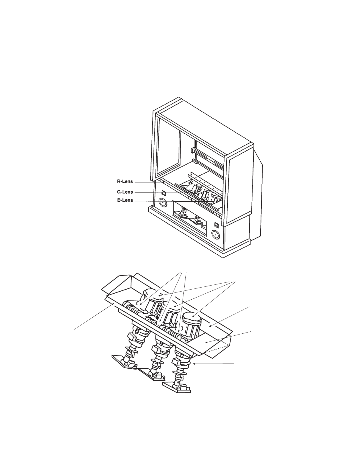
h. X-radiation Shield –
1. This receiver is provided with X-ray shield plates
for protection against X-radiation. Do not remove
X-ray shield plates A, B, or C shown in Fig. 1
unnecessarily, when troubleshooting and/or
making test measurements.
2. To prevent X-radiation, after replacement of
picture tube and lens, confirm these components
to be fixed correctly to bracket and cabinet, and
not to be taken off easily.
Shield Plate A (1.6mm)
Glass Lens for Shielding
Shield Plate B (1.6mm)
Shield Plate B (1.6mm)
Shield Plate C (1.6mm)
Detailing X-radiation shield, ( ) plate thickness
Shield Plate B (1.6mm)
Fig. 1. Installation of shield lens, shield cover and shield plates (oblique view).
Page 5

5
2. Read and comply with all caution and safety-related
notes on or inside the receiver cabinet, on the
receiver chassis, or on the picture tube.
3. Design Alteration Warning Ð Do not alter or add to
the mechanical or electrical design of this TV receiver.
Design alterations and additions including but not
limited to circuit modifications and the addition of
items such as auxiliary audio and/or video output
connectors, might alter the safety characteristics of
this receiver and create a hazard to the user. Any
design alterations or additions may void the
manufacturerÕs warranty and may make you, the
servicer, responsible for personal injury or property
damage resulting therefrom.
4. Picture Tube Implosion Protection Warning Ð The
picture tube in this receiver employs integral
implosion protection. For continued implosion
protection, replace the picture tube only with one of
the same type number. Do not remove, install, or
otherwise handle the picture tube in any manner
without first putting on shatterproof goggles equipped
with side shields. People not so equipped must be
kept safely away while picture tubes are handled.
Keep the picture tube away from your body. Do not
handle the picture tube by its neck.
5. Hot Chassis Warning Ð a. Some TV receiver chassis
are electrically connected directly to one conductor of
the AC power cord and may be safely serviced
without an isolation transformer only if the AC power
plug is inserted so that the chassis is connected to the
ground side of the AC power source. Confirm that the
AC power plug is inserted correctly with an AC
voltmeter by measuring between the chassis and a
known earth ground. If a voltage reading in excess of
1.0V is obtained, remove and reinsert the AC power
plug in the opposite polarity and again measure the
voltage potential between the chassis and a known
earth ground. b. Some TV receiver chassis normally
have 85V AC (RMS) between chassis and earth
ground regardless of the AC plug polarity. These
chassis can be safely serviced only with an isolation
transformer inserted in the power line between the
receiver and the AC power source, for both personnel
and test equipment protection. c. Some TV receiver
chassis have a secondary ground system in addition
to the main chassis ground. This secondary ground
system is not isolated from the AC power line. The two
ground systems are electrically separated by
insulating material that must not be defeated or
altered.
6. Observe original lead dress. Take extra care to assure
correct lead dress in the following areas: a. near
sharp edges, b. near thermally hot parts Ð be sure
that leads and components do not touch thermally hot
parts, c. the AC supply, d. high voltage and e. antenna
wiring. Always inspect in all areas for pinched, out-ofplate, or frayed wiring. Do not change spacing
between components and the printed circuit board.
Check AC power cord for damage.
7. Components, parts, and/or wiring that appear to have
overheated or are otherwise damaged should be
replaced with components, parts, or wiring that meet
original specifications. Additionally, determine the
cause of overheating and/or damage and, if
necessary, take corrective action to remove any
potential safety hazard.
8. PRODUCT SAFETY NOTICE Ð Many TV electrical
and mechanical parts have special safety-related
characteristics some of which are often not evident
from visual inspection, nor can the protection they
give necessarily be obtained by replacing them with
components rated for higher voltage, wattage, etc.
Parts that have special safety characteristics are
identified in Sharp service data by shading on
schematics and by a in the parts list. Use of
substitute replacement that does not have the same
safety characteristics as the recommended replacement part in Sharp service data parts list might create
shock, fire, and/or other hazards. Product safety is
under review continuously and new instructions are
issued whenever appropriate. For the latest
information, always consult the appropriate current
Sharp service literature. A subscription to, or
additional copies of service literature may be obtained
at a nominal charge from Sharp.
!
Page 6

6
CAUTION: Before servicing instruments covered by this
service data and its supplements and addenda, read and
follow the SAFETY PRECAUTIONS on page 3 of this
publication.
NOTE: If unforeseen circumstances create conflict between
the following servicing precautions and any of the safety
precautions on page 3 of this publication, always follow the
safety precautions. Remember: Safety First.
General Servicing Guidelines
1. Always unplug the instrument AC power cord from the AC
power source before:
a. Removing or reinstalling any component, circuit
board, module, or any other instrument assembly.
b. Disconnecting or reconnecting any instrument
electrical plug or other electrical connection.
c. Connecting a test substitute in parallel with an
electrolytic capacitor in the instrument.
CAUTION: A wrong part substitution or incorrect
polarity installation of electrolytic
capacitors may result in an explosion
hazard.
d. Discharging the picture tube anode.
2. Test high voltage only by measuring it with an appropriate
high voltage meter or other voltage measuring device
(DVM, FETVOM, etc.) equipped with a suitable high
voltage probe. Do not test high voltage by “drawing an
arc.” The H.V. Distribution Box has an internal 400MW
resistor (bleeder resistor) connected from the high
voltage to ground. After power is removed from the
instrument the high voltage will discharge through the
high voltage bleeder resistor. If the tubes have high
voltage after power is removed, then the bleeder resistor
is defective or the bleeder ground is disconnected.
3. Discharge the picture tube’s anode at any of the R, G, or
B outputs on the H.V. Distribution Box only by (a) first
connecting one end of an insulated clip lead to the
degaussing or kine aquadag grounding system shield at
the point where the picture tube socket ground lead is
connected, and then (b) touch the other end of the
insulated clip lead to the picture tube high voltage
distribution box R, G, or B output, using an insulated
handle to avoid personal contact with high voltage.
4. Do not spray chemicals on or near this instrument or any
of its assemblies.
5. Unless specified otherwise in these service data, clean
electrical contracts by applying the following mixture to
the contacts with a pipe cleaner, cotton-tipped stick or
comparable nonabrasive applicator: 10% (by volume)
Acetone and 90% (by volume) isopropyl alcohol (90%99% strength).
CAUTION: This is a flammable mixture. Unless
specified otherwise in these service data,
lubrication of contacts is not required.
6. Do not defeat any plug/socket B+ voltage interlocks with
which instruments covered by this service data might be
equipped.
7. Do not apply AC power to this instrument and/or any of its
electrical assemblies unless all solid-state device heatsinks are correctly installed.
8. Always connect the test instrument ground lead to the
appropriate instrument chassis ground before connecting
the test instrument positive lead. Always remove the test
instrument ground lead last.
9. Use with this instrument only the test fixtures specified in
this service data.
CAUTION: Do not connect the test fixture ground strap
to any heatsink in this instrument.
Electrostatically Sensitive (ES) Devices
Some semiconductor (solid state) devices can be damaged
easily by static electricity. Such components commonly are
called Electrostatically Sensitive (ES) Devices. Examples of
typical ES devices are integrated circuits and some fieldeffect transistors and semiconductor “chip” components. The
following techniques should be used to help reduce the
incidence of component damage caused by static electricity.
1. Immediately before handling any semiconductor
component or semiconductor-equipped assembly, drain
off any electrostatic charge on your body by touching a
known earth ground. Alternatively, obtain and wear a
commercially available discharging wrist strap device,
which should be removed for potential shock reasons
prior to applying power to the unit under test.
2. After removing an electrical assembly equipped with ES
devices, place the assembly on a conductive surface
such as aluminum foil, to prevent electrostatic charge
buildup or exposure of the assembly.
3. Use only a grounded-tip soldering iron to solder or
desolder ES devices.
4. Use only can anti-static type solder removal device.
Some solder removal devices not classified as “antistatic” can generate electrical charges sufficient to
damage ES device.
5. Do not use freon-propelled chemicals. These can
generate electrical charges sufficient to damage ES
devices.
6. Do not remove a replacement ES device from its
protective package until immediately before you are
ready to install it. (Most replacement ES devices are
packaged with leads electrically shorted together by
conductive foam, aluminum foil or comparable conductive
material.)
7. Immediately before removing the protective material from
the leads of a replacement ES device, touch the
protective material to the chassis or circuit assembly into
which the device will be installed.
CAUTION: Be sure no power is applied to the chassis or
circuit, and observe all other safety
precautions.
8. Minimize bodily motions when handling unpackaged
replacement ES devices. (Otherwise harmless motion
such as the brushing together of your clothes fabric or the
lifting of your foot from a carpeted floor can generate
SERVICING PRECAUTIONS
Page 7
7
General Soldering Guidelines
1. Use a grounded-tip, low-wattage soldering iron and
appropriate tip size and shape that will maintain tip
temperature within the range 500°F to 600°F.
2. Use an appropriate gauge of resin-core solder composed
of 60 parts tin/40 parts lead.
3. Keep the soldering iron tip clean and well-tinned.
4. Thoroughly clean the surfaces to be soldered. Use a
small wire-bristle (0.5 inch or 1.25 cm) brush with a metal
handle. Do not use freon-propelled spray-on cleaners.
5. Use the following desoldering technique.
a. Allow the soldering iron tip to reach normal
temperature (500°F to 600°F).
b. Heat the component lead until the solder melts.
Quickly draw away the melted solder with an antistatic, suction-type solder removal device or with
solder braid.
CAUTION: Work quickly to avoid overheating the
circuit board printed foil.
6. Use the following soldering technique.
a. Allow the soldering iron tip to reach normal
temperature (500°F to 600°F).
b. First, hold the soldering iron tip and solder strand
against the component lead until the solder melts.
c. Quickly move the soldering iron tip to the junction of
the component lead and the printed circuit foil, and
hold it there only until the solder flows onto and
around both the component lead and the foil.
CAUTION: Work quickly to avoid overheating the
circuit board printed foil or components.
d. Closely inspect the solder area and remove any
excess or splashed solder with a small wire-bristle
brush.
Removal
1. Desolder and straighten each IC lead in one operation by
gently prying up on the lead with the soldering iron tip as
the solder melts.
2. Draw away the melted solder with an anti-static suctiontype solder removal device (or with solder braid) before
removing the IC.
Replacement
1. Carefully insert the replacement IC in the circuit board.
2. Carefully bend each IC lead against the circuit foil pad
and solder it.
3. Clean the soldered areas with a small wire-bristle brush.
(It is not necessary to reapply acrylic coating to areas.)
“Small-signal” Discrete Transistor Removal/Replacement
1. Remove the defective transistor by clipping its leads as
close as possible to the component body.
2. Bend into a “U” shape the end of each of three leads
remaining on the circuit board.
3. Bend into a “U” shape the replacement transistor leads.
4. Connect to replacement transistor leads to the
corresponding leads extending from the circuit board and
crimp the “U” with long nose pliers to insure metal to
metal contact, then solder each connection.
Power Output Transistor Devices Removal/Replacements
1. Heat and remove all solder from around the transistor
leads.
2. Remove the heatsink mounting screw (if so equipped).
3. Carefully remove the transistor from the circuit board.
4. Insert new transistor in circuit board.
5. Solder each transistor lead, and clip off excess lead.
6. Replace heatsink.
Diode Removal/Replacement
1. Remove defective diode by clipping its leads as close as
possible to diode body.
2. Bend the two remaining leads perpendicularly to the
circuit board.
3. Observing diode polarity, wrap each lead of the new
diode around the corresponding lead on the circuit board.
4. Securely crimp each connection and solder it.
5. Inspect (on the circuit board copper side) the solder joints
of the two “original leads”. If they are not shiny, reheat
them and, if necessary, apply additional solder.
Use Solding Iron to Pry Leads
IC Removal/Replacement
Some Sharp unitized chassis circuit boards have slotted
holes (oblong) through which the IC leads are inserted and
then bent flat against the circuit foil. When holes are the
slotted type, the following technique should be used to
remove and replace the IC. When working with boards using
the familiar round hole, use the standard technique as
outlined in paragraphs 5 and 6 above.
Page 8
8
Fuses and Conventional Resistor Removal/Replacement
1. Clip each fuse or resistor lead at top of circuit board
hollow stake.
2. Securely crimp leads of replacement component around
stake 1/8 inch from top.
3. Solder the connections.
CAUTION: Maintain original spacing between the
replaced component and adjacent
components and the circuit board, to
prevent excessive component
temperatures.
Circuit Board Foil Repair
Excessive heat applied to the copper foil of any printed
circuit board will weaken the adhesive that bonds the foil to
the circuit board, causing the foil to separate from, or Òliftoff,Ó the board. The following guidelines and procedures
should be followed whenever this condition is encountered.
In Critical Copper Pattern Areas
High component/copper pattern density and/or special
voltage/current characteristics make the spacing and
integrity of copper pattern in some circuit board areas more
critical than in others. The circuit foil in these areas is
designated as Critical Copper Pattern. Because Critical
Copper Pattern requires special soldering techniques to
ensure the maintenance of reliability and safety standards,
contact your Sharp personnel.
At IC Connections
To repair defective copper pattern at IC connections, use the
following procedure to install a jumper wire on the copper
pattern side of the circuit board. (Use this technique only on
IC connections.)
1. Carefully remove the damaged copper pattern with a
sharp knife. (Remove only as much copper as absolutely
necessary.)
2. Carefully scratch away the solder resist and acrylic
coating (if used) from the end of the remaining copper
pattern.
3. Bend a small ÒUÓ in one end of a small-gauge jumper wire
and carefully crimp it around the IC pin. Solder the IC
connection.
4. Route the jumper wire along the path of the cut-away
copper pattern and let it overlap the previously scraped
end of the good copper pattern. Solder the overlapped
area, and clip off any excess jumper wire.
1. Remove the defective copper pattern with a sharp knife.
Remove at least 1/4 inch of copper, to ensure hazardous
condition will not exist if the jumper wire opens.
2. Trace along the copper pattern from both wire sides of
the pattern break and locate the nearest component
directly connected to the affected copper pattern.
3. Connect insulated 20-gauge jumper wire from the
nearest component on one side of the pattern break to
the lead of the nearest component on the other side.
Carefully crimp and solder the connections.
CAUTION: Be sure the insulated jumper wire is
dressed so that it does not touch
components or sharp edges.
Frequency Synthesis (FS) Tuning Systems
1. Always unplug the instrument AC power cord before
disconnecting or reconnecting FS tuning system cables
and before removing or inserting FS tuning system
modules.
2. The FS tuner must never be disconnected from the FS
tuning control module while power is applied to the
instrument.
3. When troubleshooting intermittent problems that might be
caused by defective cable connection(s) to the FS tuning
system, remove the instrument AC power as soon as the
defective connector is found and finish confirming the
bad connection with a continuity test. This procedure will
reduce the probability of electrical overstress of the FS
system semi-conductor components.
CRIMP AND
SOLDER
BARE JUMPER
WIRE
Install Jumper Wire and Solder
DEFECTIVE
COPPER
REMOVED
Insulated Jumper Wire
At Other Connections
Use the following technique to repair defective copper
pattern at connections other than IC Pins. This technique
involves the installation of a jumper wire on the component
side of the circuit board.
Page 9

9
Leadless Chip Components
(surface mount)
Chip components must be replaced with identical
chips due to critical foil track spacing. There are no
holes in the board to mount standard transistors or
diodes. Some chip capacitor or resistor board solder
pads may have holes through the board, however the
hole diameter limits standard resistor replacement to
1/8 watt. Standard capacitors may also be limited for
the same reason. It is recommended that identical
chip components be used. .
Chip resistors have a three digit numerical resistance
code -1st and 2nd significant digits and a multiplier.
Example: 162 = 1600 or 1.6KΩ resistor, 0 = 0Ω
(jumper).
Chip capacitors generally do not have the value
indicated on the capacitor. The color of the component
indicates the general range of the capacitance.
Chip transistors are identified by a two letter code. The
first letter indicates the type and the second letter, the
grade of transistor.
Chip diodes have a two letter identification code as
per the code chart and are a dual diode pack with
either
common anode or common cathode. Check the parts
list for correct diode number.
Component Removal
1. Use solder wick to remove solder from component
end caps or terminals.
2. Without pulling up, carefully twist the component
with tweezers to break the adhesive.
3. Do not reuse removed leadless or chip
components since they are subject to stress
fracture during removal .
Chip Component Installation
1. Put a small amount of solder on the board
soldering pads.
2. Hold the chip component against the soldering
pads with tweezers or with a miniature alligator
clip and apply heat to the pad area with a 30 watt
iron until solder flows. Do not apply heat for more
than 3 seconds
How to Replace Flat-lC
—Required Tools—
• Soldering iron • iron wire or small awl
• De-solder braids • Magnifier
1. Remove the solder from all of the pins of a Flat-lC
by using a de-solder braid.
2. Put the iron wire under the pins of the Flat-lC and
pull it in the direction indicated while heating the
pins using a soldering iron. A small awl can be
used instead of the iron wire.
3. Remove the solder from all of the pads of the
Fiat-lC by using
a de-solder braid.
4. Position the new Flat-lC in place (apply the pins of
the Flat-lC to the soldering pads where the pins
need to be soldered). Properly
determine the positions of the
soldering pads and pins by
correctly aligning the polarity
symbol.
6. Check with a magnifier for solder bridge between
the pins or for dry joint between pins and soldering
pads. To remove a solder bridge, use a de-solder
braid as shown in the figure below.
NOTE:
These components are affixed with glue. Be careful not to break or damage any foil under the
component or at the pins of the ICs when removing. Usually applying heat to the component for a short
time while twisting with tweezers will break the component loose.
Chip Components
TYPE
GRADE
C
B
E
SOLDER
CAPS
TRANSISTOR
CAPACITOR
1ST DIGIT
2ND DIGIT
MULTIPLIER
= 1600 = 1.6K
ANODES
MH DIODE
RESISTOR
SOLDER CAPS
COMMON CATHODE
De-Solder
Braid
Soldering
Iron
Soldering
Iron
Soldering
Iron
Soldering
Iron
Soldering
Iron
Soldering
Iron
De-Solder
Braid
Flat-IC
Bridge
Solder
De-Solder
Braid
Iron
Wire
Pull
Awl
Polarity Symbol
5. Solder all pins to the soldering pads using a fine
tipped soldering iron.
Page 10
10
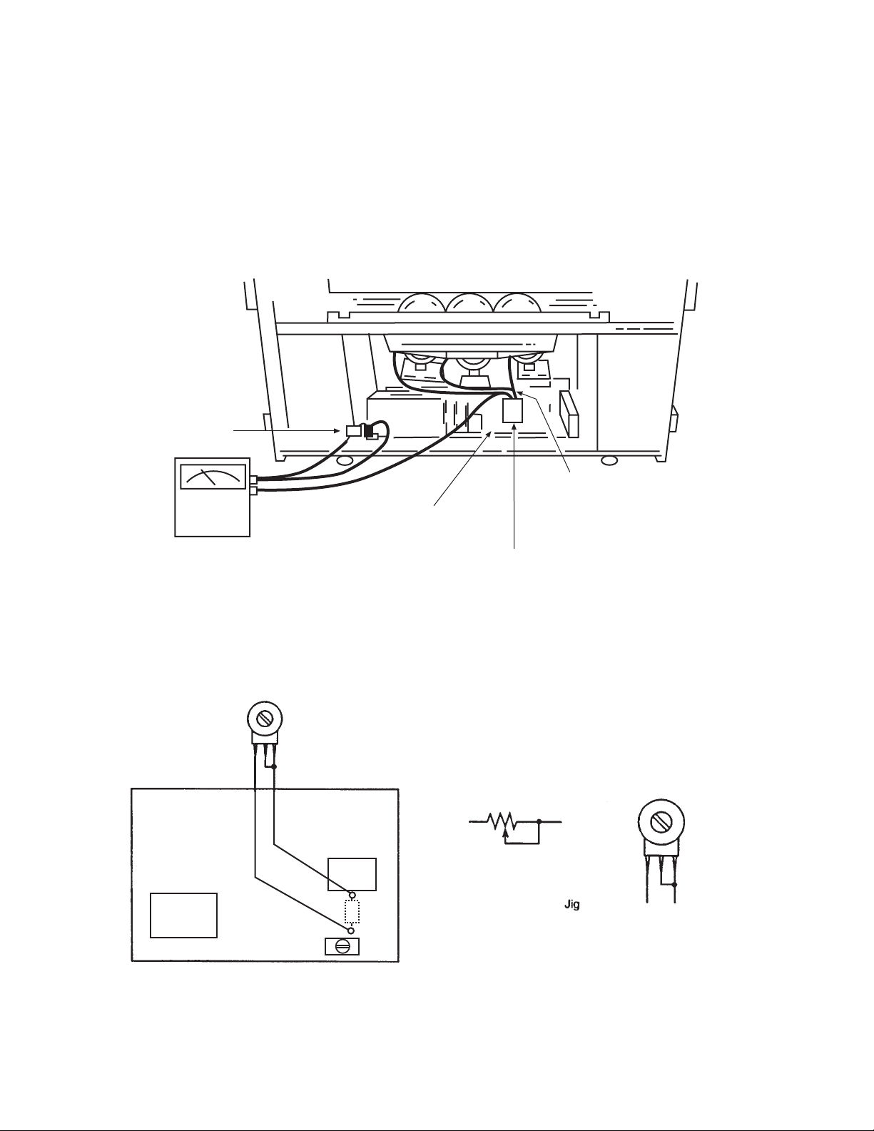
High Voltage limiter circuit operation check.
1. Turn off TV and connect jig as shown in Figure 2. Adjust
jig fully counter-clockwise for minimum resistance.
2. Set the AC input to 120V AC and turn on TV.
3. Confirm test pattern on CRT is a usable picture, then
slowly adjust jig until the picture disappears and TV shuts
down.
4. When the limiter circuit is operating properly, High
Voltage will be less than 31.5 kV at 1.5mAwhen TV shuts
down.
5. Turn off set immediately after checking circuit operation.
6. Unplug set for one minute to reset shutdown circuit.
Remove jig and voltmeter.
TECHNICAL CAUTIONS
TP91
CP16
IP04
Remove RH80 and connect 50KΩVR jig as shown.
FBT
RH80
TP91
POWER/DEFLECTION PWB
RH44
50K½VR
Fig. 2. Deflection/Power P.C.B.
Chassis ground
Deflection P.W.B.
High voltage
connector
High impedance
H.V. meter
FBT
(TH01)
Page 11
11
Model: 50NP4 60NP4
Cathode-Ray Tube:
R=P16LFM00RFA(LU)
G=P16LFM00HHA(LU)
B=P16LFM00BMB(EU)
Power Input: 120 volts AC, 60 Hz
Power Consumption: 50NP4 60NP4
Maximum 232W 232W
Operating 206W 206W
Antenna Impedance: 75 Ohm Unbalanced
VHF / UHF / CATV
Receiving Channel: BAND CH
VHF 2~13
UHF 14~69
EXT. Mid (A-5)~(A-1), 4+
CATV Mid. A~I
CATV Super J~W
CATV Hyper (W+1)~(W+28)
Intermediate Frequency: Picture l-F Carrier 45.75 MHz
Sound l-F Carrier 41.25 MHz
Color Sub Carrier 42.17 MHz
Video Input: 1 Volt p-p, 75 Ohm
1 Volt p-p, 75 Ohm (Y)
0.7 Volt p-p, 75 Ohm, (P
B
, PR)
Video Output: 1 Volt p-p, 75 ohm
Audio Input: 470 mVrms, 47 k Ohm
Stereo Audio Output: 470 mVrms, 1 k Ohm
Audio Output Power:
Front: 12 watts per channel at 10% distortion,
8 ohm Impedance. Max output Ð 15 watts.
Anode Voltage: 30.0 ± 1.5kv (1.27±0.2mA)
Brightness: 50NP4 130cd/m2
60NP4 100cd/m2
Speakers:
2 Woofers - 5 inch (120 mm) round
Dimension: 50NP4 60NP4
Height (in.) 51
7
/
8
60
2
/
5
Width (in.) 43
1
/
5
51
1
/
3
Depth (in.) 23
3
/
5
26
2
/
3
Weight (Ibs.) 145 216
Circuit Board Assemblies:
C.P.T. (B) P.W.B. Terminal P.W.B.
C.P.T. (G) P.W.B. VM P.W.B.
C.P.T. (R) P.W.B. Surround P.W.B.
Audio Out P.W.B. Power/Deflection P.W.B.
2 H P.W.B. Control P.W.B.
Power Supply P.W.B. Control Sub P.W.B.
Signal P.W.B. Sensor Distribution P.W.B.
Sub Deflection P.W.B.
CIRCUIT PROTECTION
CAUTION: Below is an EXAMPLE only. See Replacement Parts List for details. The following symbol near the fuse
indicates fast operation fuse (to be replaced). Fuse ratings appear within the symbol.
Example:
SPECIFICATIONS
RISK OF FIRE - REPLACE FUSE AS MARKED
The rating of fuse F901 is 6.0A - 125V.
Replace with the same type fuse for continued protection
against fire.
F
6 A 125V
125V
6A
Page 12
12
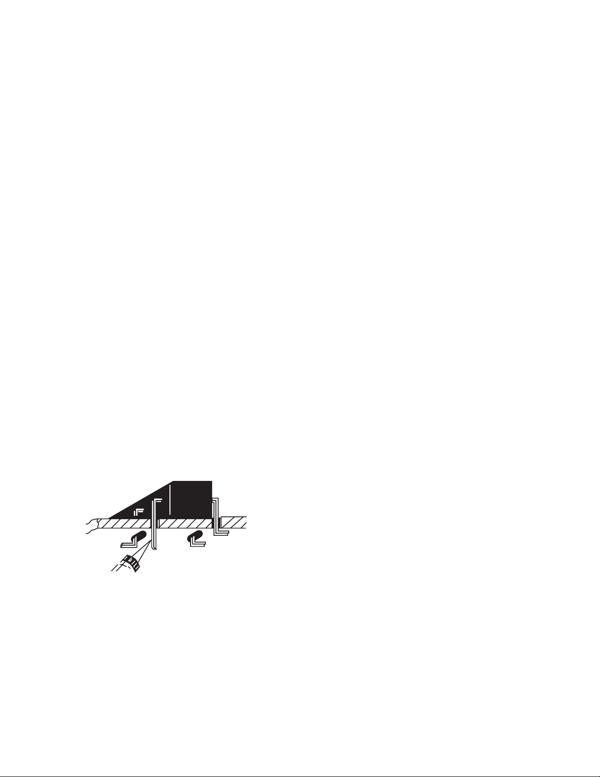
During Insertion
1. Please refer to direction for insertion as shown in Fig. B (L position). Insert connector until “CLICK” sound is heard.
2. Make sure the connector is pressed right in, so that it has a good contact with the spring.
3. Confirm the contact by pulling the connector slightly. (Don’t pull hard because it may damage the connector).
4. Cover the high voltage output by carefully pushing silicon cover onto it. (Don’t turn the connector).
(REMARK)
1. Make sure the silicon cover is
covering the high voltage output.
CAUTIONS WHEN CONNECTING / DISCONNECTING THE HV CONNECTOR
Perform the following when the
HV connector (anode connector)
is removed or inserted for CPT
replacement, etc.
Deflection P.W.B.
Silicon cover
Wing
L Position
L Position
Wing
FBT
Anode
connector
3. Remove the connector slowly
by pulling it away from the
case.
During Removal
1. Roll out silicon cover from FBT’s contact area slowly .
2. While turning the connector about 90 degrees
following the arrow (0 position), push the connector
slightly towards the case. (Fig. A)
Fig. A
Fig. B
Silicon Cover
less than 1mm
PUSH
PUSH
Page 13
13
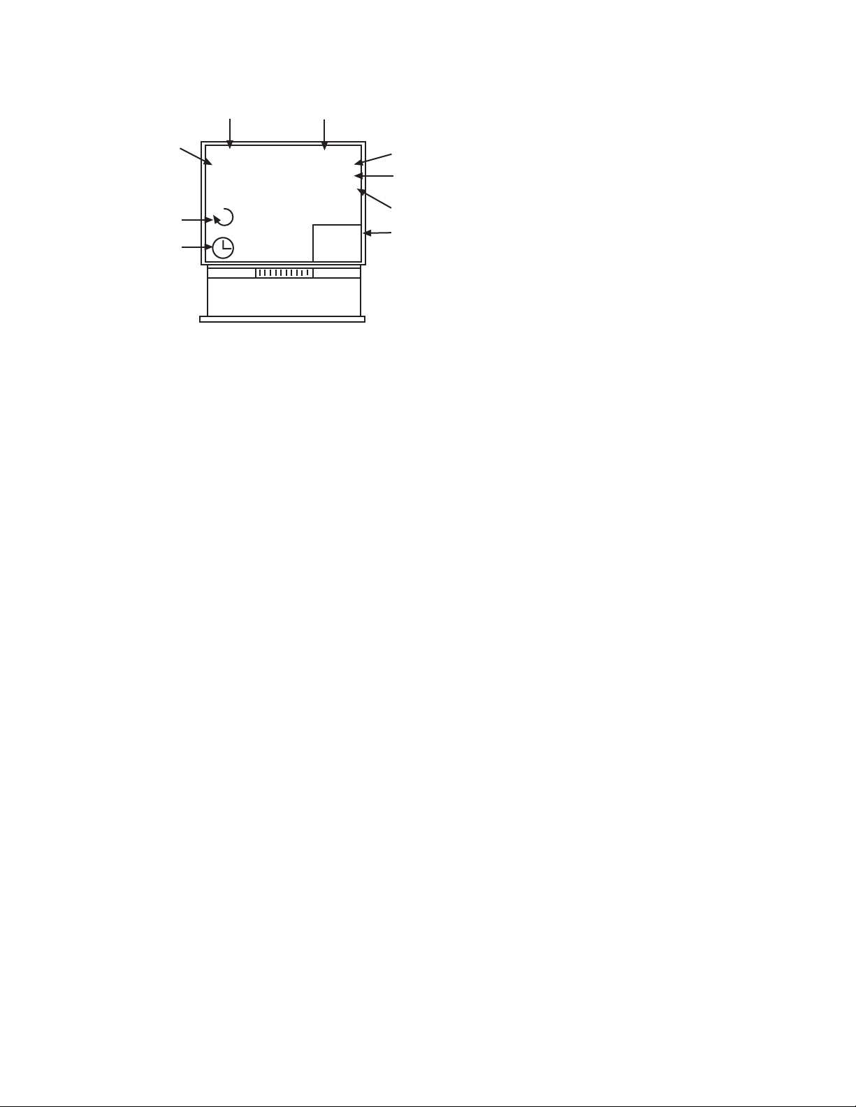
FRONT PANEL CONTROLS
FRONT VIEW
POWER
INPUT
EXIT
MENU
f e b a c
d i j
Push open door and
pull forward and down
PUSH
POWER
INPUT
h
g
EXIT MENU
VOL+VOL-
CH-
CH+
VOL+VOL-
CH-
CH+
SCREEN
ADJ.
POWER
INPUT
EXIT
MENU
PUSH
VOL+VOL-
CH-
CH+
NOTES: 1. Your SHARP Projection TV will appear to be turned OFF if there is no video input when VIDEO: 1, 2 or 3 is
selected. Check the Power Light to make sure the TV is turned off when not in use.
2. To see an auto-demonstration of the on-screen displays with HELP text displayed, press and hold the POWER
button on the TV set for approximately five seconds. Press the POWER button on the TV again to end the autodemonstration.
a MENU button
This button allows you to enter the MENU, making it possible to set TV features to your preference without using the remote. This
button also serves as the ÒSELECTÓ button when in menu mode.
b INPUT/EXIT button
Press this button to select the current antenna source, VIDEO: 1, 2, 3 or alternate antenna source. Your selection is shown in the
top right corner of the screen. This button also serves as the EXIT button when in MENU mode.
c CHANNEL selector
Press these buttons until the desired channel appears in the top right corner of the TV screen. These buttons also serve as
the cursor down (H) and up (G) buttons when in MENU mode.
d VOLUME level
Press these buttons for your desired sound level. The volume level will be displayed on the TV screen. These buttons also serve
as the cursor left (F) and right (E) buttons when in MENU mode.
e POWER button
Press this button to turn the TV on or off.
Page 14

14
f POWER light
You will see a red light when the TV is turned on.
g AI (Artificial Intelligence) sensor
The Artificial Intelligence sensor will make automatic picture adjustments depending on the amount of light in the room to give the
best picture.
h REMOTE CONTROL sensor
Point your remote at this area when selecting channels, adjusting volume, etc.
i SCREEN ADJUST
Use this button to adjust your picture quality to optimum performance.
j FRONT INPUT JACKS (for VIDEO: 3)
Use these audio/video jacks for a quick hook-up from a camcorder or VCR to instantly view your favorite show or new recording.
Press the INPUT button until VIDEO: 3 appears in the top right corner of the TV screen. If you have mono sound, insert the audio
cable into the left audio jack.
FRONT PANEL CONTROLS
Page 15
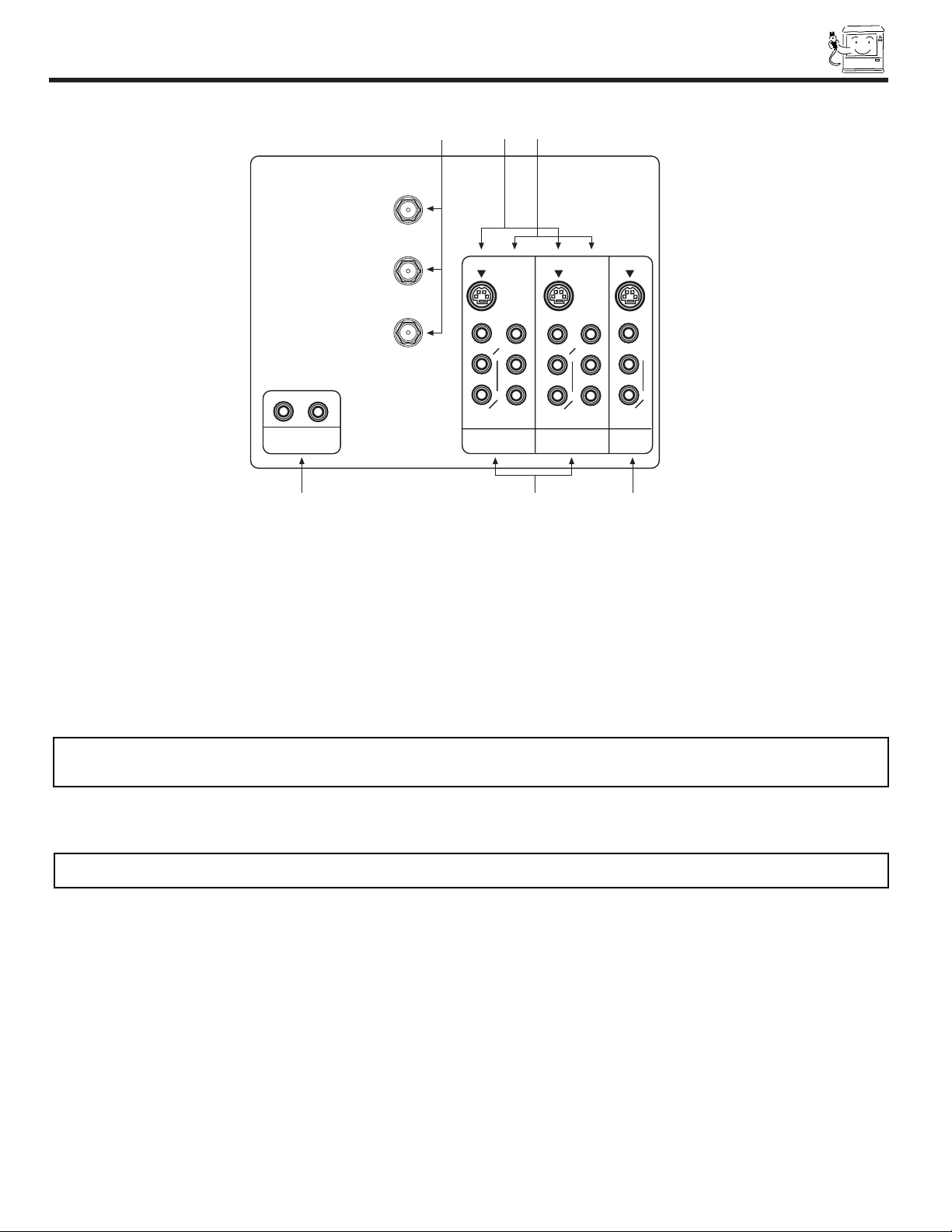
REAR PANEL JACKS
a Antenna Input/Output
The remote control allows you to switch between two separate 75-Ohm RF antenna inputs, ANT A and ANT B. ANT A input can
be displayed as a main picture or sub-picture. ANT B can only be displayed as a main picture. (ANT B cannot be displayed as a
sub-picture.) The antenna output labeled ÒTO CONVERTERÓ allows the ANT A connection to pass directly to a different source
such as a cable box, only when ANT B is displayed as a main picture.
b Audio/Video Inputs 1 and 2
The INPUT button will step through each video source and antenna source input each time it is pressed. Use the audio and video
inputs to connect external devices, such as VCRs, camcorders, laserdisc players, DVD players etc. (If you have mono sound, insert
the audio cable into the left audio jack.)
c MONITOR OUT
These jacks provide fixed audio and video signals which are used for recording. Use the S-VIDEO Output for high quality video
output.
d AUDIO TO HI-FI Output
These jacks provide variable audio output to a separate stereo amplifier. With this connection, the audio to the stereo can be
controlled by the televisionÕs main volume.
e S-VIDEO Inputs 1 and 2
Inputs 1 and 2 provide S-VIDEO (Super Video) jacks for connecting equipment with S-VIDEO output capability.
a
b
c
e
P
B
P
R
P
B
P
R
f
d
MONITOR
OUT
INPUT 2
INPUT 1
AUDIO
(MONO)
L
R
AUDIO
L
R
S-VIDEOS-VIDEO
VIDEO
VIDEO
ANT A
TO
CONVERTER
ANT B
AUDIO
L
R
(MONO)
S-VIDEO
VIDEO
YY
AUDIO
TO HI-FI
R
L
NOTE: You may use VIDEO, S-VIDEO, or COMPONENT: Y-PBPRinputs to connect to INPUT 1 and 2, but only one of these
inputs may be used at a time.
NOTE: S-VIDEO Output may be used for recording, only when the input is of S-VIDEO type.
15
Page 16

16
REAR PANEL JACKS
NOTES: 1.
DO NOT connect standard VIDEO or S-VIDEO to Input 1 or 2 when using Y-PBPRinput.
2. When using the Y-PBPRinput jacks, connect your components audio output to the TVÕs Input 1 or 2 Left and Right Audio input jacks.
3. Your component outputs may be labeled Y, B-Y, and R-Y. In this case, connect the components B-Y output to the TVÕs PBinput and
the components R-Y output to the TVÕs PRinput.
4. Your component outputs may be labeled Y-CBCR. In this case, connect the component CBoutput to the TVÕs PBinput and the
component CRoutput to the TVÕs PRinput.
5. It may be necessary to adjust TINT to obtain optimum picture quality when using the Y-PBPR inputs.
6. To ensure no copyright infringement, the MONITOR OUT output will be abnormal, when using the Y-PBPRjacks.
7. When using the Y-PBPR jacks, PIP sub-picture can not be turned ON. It is not possible to view a Y-PBPRinput while PIP is ON.
f Component: Y-P
BPR
Inputs
Inputs 1 and 2 provide Y-P
BPR
jacks for connecting equipment with this capability, such as a DVD player or Set Top Box.
Page 17
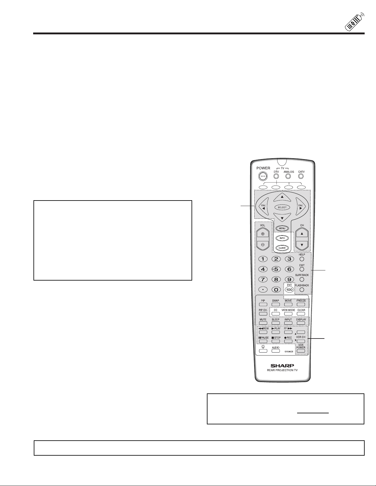
USING THE REMOTE TO CONTROL VCR FUNCTIONS
Operating the precoded function for your VCR.
This remote is designed to operate different types of VCRs. You must first program the remote to match the remote system of your
VCR. (refer to page 18 for pre-codes)
1. Turn ON your VCR.
2. Aim the remote control at the front of your VCR.
3. Press and release the ANALOG mode button.
4. Push ÒSELECTÓ key and ÒCH HÓ key at the same time, then release both buttons, and within 10 seconds after releasing these
buttons, enter the 2 digit code number as shown on page 31.
5. Aim the remote at the VCR and press the POWER button. The remote will turn off your VCR when the correct two digit preset code
is entered. When this occurs, the remote control is programmed for your VCR. If the VCR does not turn off, try a different two digit
preset code.
6. The remote will now control your VCR.
NOTES:
1. If your VCR cannot be operated after performing the
above procedures, your VCRÕs code has not been
precoded into the remote.
2. In the unlikely event that your VCR cannot be operated
after performing the above procedures, please consult
your VCR operating guide.
3. The remote control will remember the codes you have
programmed until the batteries are removed from the
remote control. After replacing the batteries repeat the
entire programming procedure as stated above.
a PRECODED VCR Buttons
These buttons transmit the chosen precoded VCR codes.
For some VCRs, you must press the RECORD button twice
to record a program.
b EXCLUSIVE TV Buttons
These buttons are for operating the TV.
b
b
a
MY VCR CODE IS:
NOTE: Refer to the instruction manual of the VCR for operation of the buttons exclusively for the VCR.
17
Page 18

18
VCR BRAND. . . . . . . . . . . . . CODE
Akai . . . . . . . . . . . . . . . . . 25, 26, 37
Audio Dynamics . . . . . . . . 15, 22, 30
Broksonic . . . . . . . . . . . . . . . . . . 32
Canon . . . . . . . . . . . . . . . . . . . . . 04
Capehart . . . . . . . . . . . . . . . . . . . 34
Craig . . . . . . . . . . . . . . . . . . . . . . 31
Curtis Mathis . . . . . . . . . . . . . . . . 04
Daewoo . . . . . . . . . . . . . . . . . . . . 34
DBX. . . . . . . . . . . . . . . . . 15, 22, 30
Dynatech . . . . . . . . . . . . . . . . . . . 29
Emerson . . . . . . . . . . . . . 21, 32, 35
Fisher . . . . . . . . . . . . . . . . . . 09, 11
Funai . . . . . . . . . . . . . . . . . . . . . . 29
GE. . . . . . . . . . . . . . . . . . . . . . . . 04
Goldstar. . . . . . . . . . . . . . . . . . . . 24
Hitachi . . . . . . . . . . . . . . . . . . . . . 06
Instant Replay . . . . . . . . . . . . . . . 04
JC Penney . . . . . . . . . 04, 06, 24, 30
JVC . . . . . . . . . . . . . . . . . 15, 41, 42
Kenwood . . . . . . . . . . . . . . . . . . . 15
Lloyds . . . . . . . . . . . . . . . . . . . . . 29
Magnavox . . . . . . . . . . . . 04, 05, 08
Magnin . . . . . . . . . . . . . . . . . . . . 31
Marantz . . . . . . . . . . . . . . . . . . . . 30
Memorex . . . . . . . . . . . . . 04, 24, 29
Minolta . . . . . . . . . . . . . . . . . . . . 06
Mitsubishi. . . . . . . . . . 17, 18, 39, 40
Montgomery Ward . . . . . . . . . 02, 43
Multitech . . . . . . . . . . . . . . . . . . . 29
NEC. . . . . . . . . . . . . . . . . 15, 22, 30
Panasonic . . . . . . . . . . . . . . . 04, 44
Pentax . . . . . . . . . . . . . . . . . . 05, 06
Philco . . . . . . . . . . . . . . . . . . 04, 05
Philips . . . . . . . . . . . . . . . 04, 05, 08
Quasar . . . . . . . . . . . . . . . . . . . . 04
RCA. . . . . . . . . . . . . . . . . 06, 07, 33
Realistic . . . . . . . . . . . . . . 01, 02, 24
Samsung . . . . . . . . . . . . . . . . 23, 31
Scott . . . . . . . . . . . . . . . . . . . . . . 20
Sears . . . . . . . . . . . . . . . . 06, 11, 24
Sharp. . . . . . . . . . . . . . . . 01, 02, 03
Shintom . . . . . . . . . . . . . . . . . . . . 36
Sony . . . . . . . . . . . . . . . . 12, 13, 38
Sound Design . . . . . . . . . . . . . . . 29
Sylvania . . . . . . . . . . . . . . 04, 05, 08
Symphonic. . . . . . . . . . . . . . . . . . 29
Tatung . . . . . . . . . . . . . . . . . . . . . 15
Teac . . . . . . . . . . . . . . . . . . . 15, 29
Teknika . . . . . . . . . . . . . . . . . 27, 29
Thomas . . . . . . . . . . . . . . . . . . . . 29
TMK . . . . . . . . . . . . . . . . . . . . . . 21
Toshiba . . . . . . . . . . . . . . . . . 19, 20
Video Concepts . . . . . . . . . . . . . . 30
Yamaha . . . . . . . . . . . . . . 15, 29, 30
Zenith . . . . . . . . . . . . . . . . . . . . . 16
CABLE BRAND . . . . . . . . . . CODE
Anision . . . . . . . . . . . . . . . . . 07, 08
Cable Star . . . . . . . . . . . . . . . 07, 08
Eagle. . . . . . . . . . . . . . . . . . . . . . 08
Eastern International . . . . . . . . . . 02
General Instrument . . 04, 05, 15, 23,
. . . . . . . . . . . . . . . . . 24, 25, 30, 36
Hamliln . . . . . . . . . . . . . . 12, 13, 34
Jerold . . . . . . . . . . . . 04, 05, 15, 23,
. . . . . . . . . . . . . . . . . 24, 25, 30, 36
Macom . . . . . . . . . . . . . . . . . . . . 37
Magnavox . . . 07, 08, 19, 25, 28, 29,
. . . . . . . . . . . . . . . . . 32, 33, 40, 41
NSC . . . . . . . . . . . . . . . . . . . . . . 09
Oak . . . . . . . . . . . . . . . . . 01, 16, 38
Oak Sigma . . . . . . . . . . . . . . . . . 18
Panasonic . . . . . . . . . . . . . . . 27, 39
Philips . . . . . . 07, 08, 19, 26, 28, 29,
. . . . . . . . . . . . . . . . . 32, 33, 40, 41
Pioneer . . . . . . . . . . . . . . . . . 18, 20
Randtek . . . . . . . . . . . . . . . . . 07, 08
RCA . . . . . . . . . . . . . . . . . . . . . . 27
Regal. . . . . . . . . . . . . . . . . . . 12, 13
Regency . . . . . . . . . . . . . . . . . . . 02
Scientific Atlanta. . . . . . . . 03, 22, 42
Sylvania. . . . . . . . . . . . . . . . . . . . 11
Teknika . . . . . . . . . . . . . . . . . . . . 06
Texscan . . . . . . . . . . . . . . . . . . . . 11
Tocom . . . . . . . . . . . . . . . . . . 17, 21
Unika. . . . . . . . . . . . . . . . . . . . . . 31
Viewstar. . 07, 08, 19, 26, 28, 29, 32,
. . . . . . . . . . . . . . . . . . . . 33, 40, 41
Zenith . . . . . . . . . . . . . . . . . . . . . 14
VCR and CABLE CODES
Page 19
19
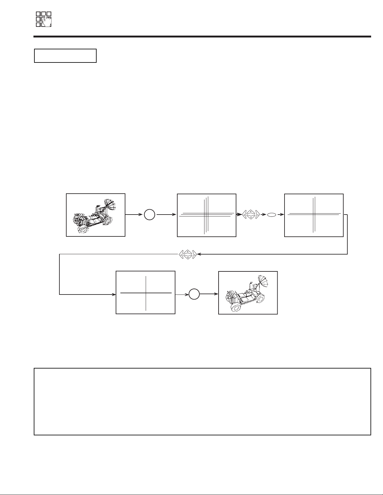
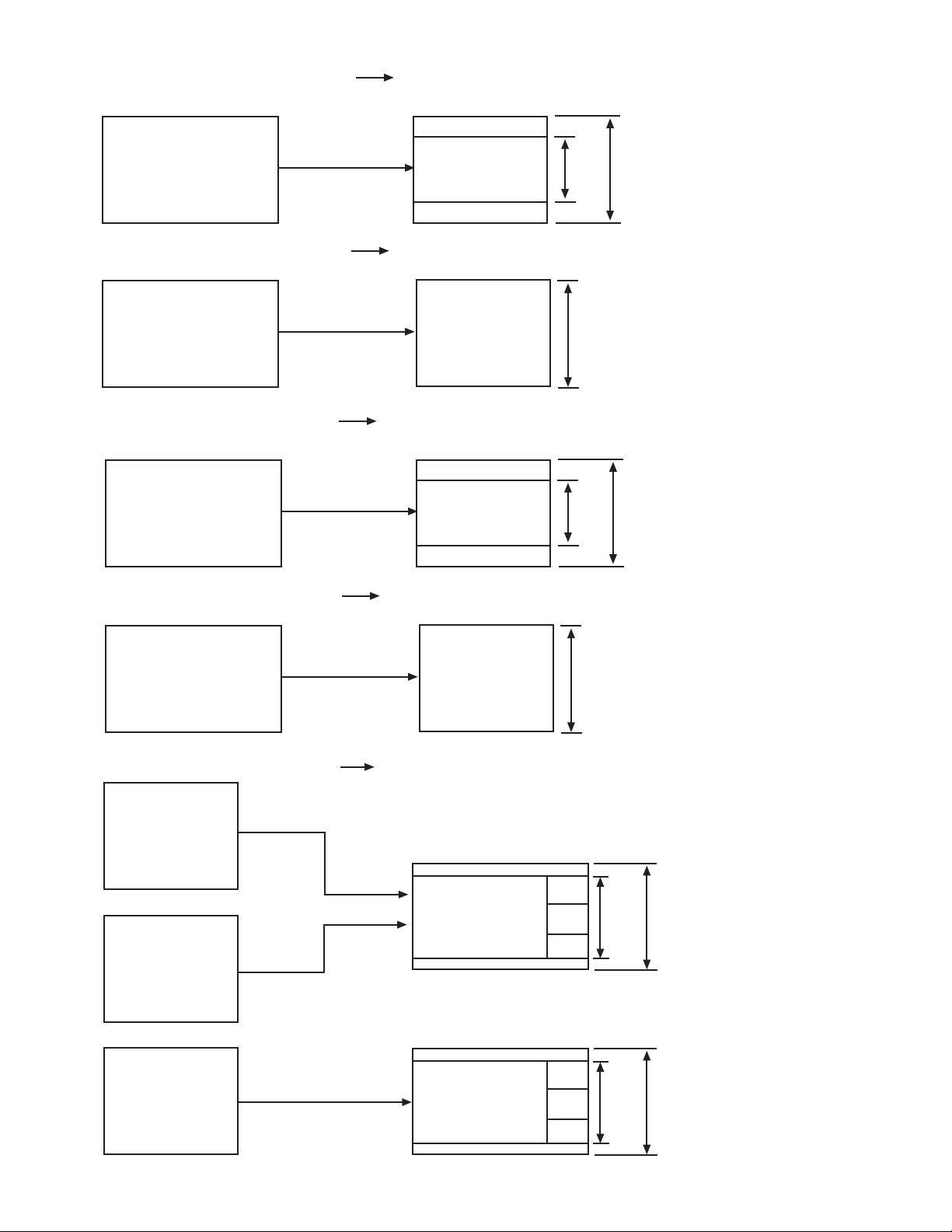
SET UP
SET UP
Your SHARP Projection TV has three color projection tubes: one for red, one for green, one for blue. When mixed together in the proper
proportion, the output of these three color tubes can produce any color. To produce these colors, however, the beams must be precisely
aligned over each other so that the colors can be mixed. The process of aligning these picture beams is called ÒconvergenceÓ.
Over a period of time, the picture tubes can drift out of alignment due to normal bumps and vibrations or moving the TV. If you move
your TV, or if, after a time, you notice color rings or halos around objects in the picture, you may want to converge (align) the colors.
Properly converged, the lines appear white, which is actually a combination of the outputs of the three color tubes. The output of the
green tube is stationary. The outputs of the red and blue tubes can be adjusted. When properly aligned, the outputs of all three tubes
should be directly over each other to produce the white lines.
To simplify convergence, SHARP incorporates a feature to allow you to display a test pattern of 1 horizontal and 1 vertical line at the
center of the screen. Simply use the remote control to adjust the red and blue colors to match the green. When properly aligned, the
outputs of all three tubes should be directly over each other to produce the white lines.
To enter this adjustment mode, you may also select CONVERGENCE ADJ. from the Set Up menu. However, this will display a message
prompting you to press the front panel SCREEN ADJ. button.
NOTES: 1. Only a momentary press of the SCREEN ADJ. button is necessary to enter CONVERGENCE ADJUST mode.
2. The color being adjusted will blink (red or blue) to indicate color you are adjusting.
3. To save your adjustment data into memory, press the front panel SCREEN ADJ. button. If you do NOT wish to save
your adjustment data into memory, turn the TV OFF. When the TV is turned ON again, your old convergence data
will be restored.
CONVERGENCE ADJ.
Red
SCREEN
ADJ.
Blue
SCREEN
ADJ.
CURSOR
FAV.
FAV.
MENU
CURSOR
FAV.
FAV.
Press the CURSOR G , H , F , E buttons to move the displayed color up, down, left, or right.
Press MENU to change the color you want to adjust.
Press the front panel SCREEN ADJ. button when adjustment is done. This will save your adjustment into memory.
Page 20

20
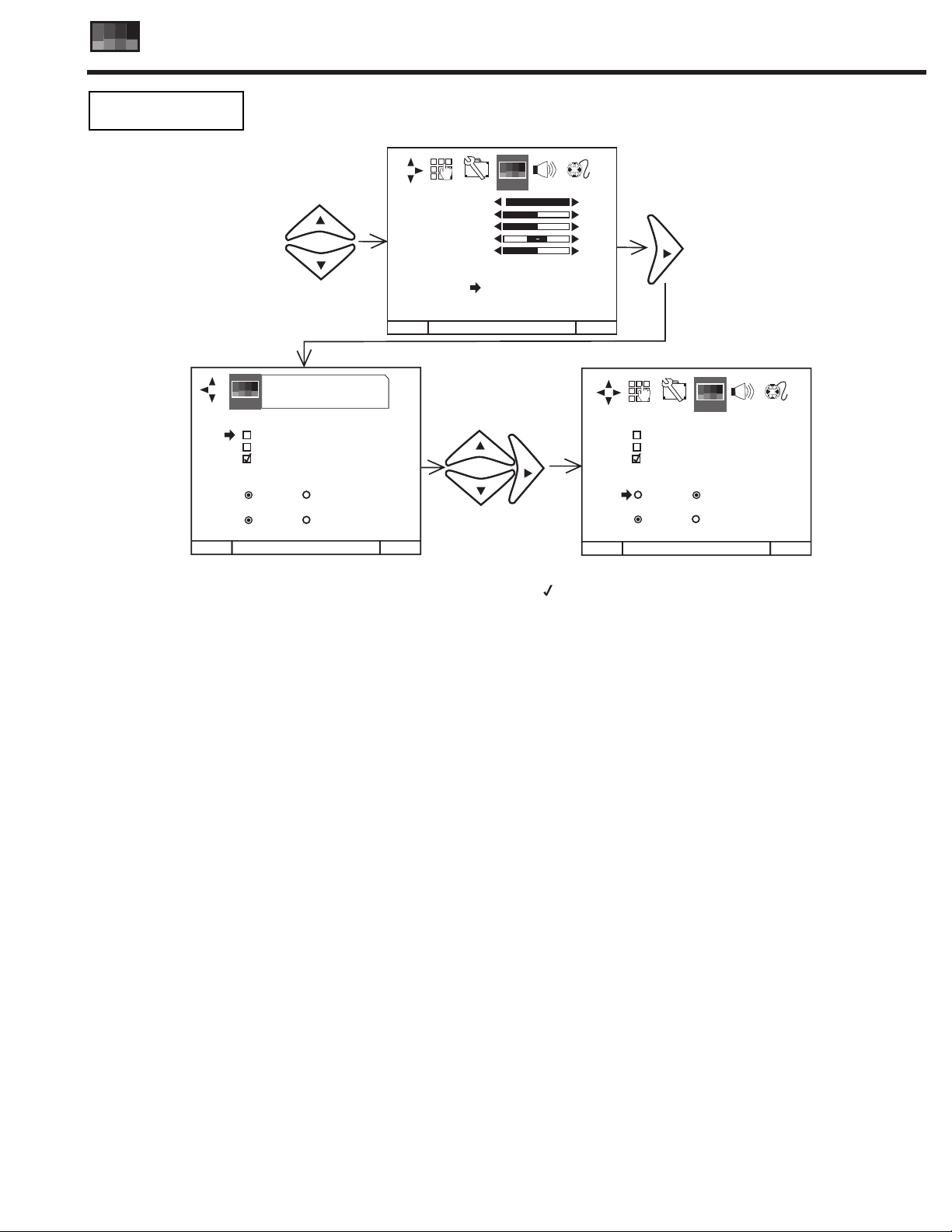
VIDEO
VIDEO
VIDEO
Select VIDEO to adjust picture settings and improve picture quality.
Use this function to change the contrast between black and white levels in the picture. This adjustment will
only affect the picture when OTHER SETTINGS-O.P.C. is OFF. (see page 50)
Use the CURSOR G or H to highlight the function to be adjusted.
Press the CURSOR F or E to adjust the function.
Press EXIT to quit menu.
NOTE: If PICTURE is selected, you are adjusting the PICTURE. The additional menu items BRIGHT, COLOR, TINT,
and SHARP can be selected and adjusted in the same manner.
Use this function to adjust the level of color in the picture.
Use this function to adjust flesh tones so they appear natural.
Use this function to adjust overall picture brightness.
Use this function to adjust the amount of fine detail in the picture.
When RESET is selected, press SELECT to return video adjustments to factory preset conditions.
PICTURE
COLOR
TINT
BRIGHT
SHARP
RESET
NOTE: 1. It may be necessary to adjust TINT to obtain optimum picture quality when using the COMPONENT VIDEO Y-PBP
R
input jacks.
2. If you are using the COMPONENT VIDEO input jacks (Y-PBPR) and notice that the TINT and COLOR are abnormal,
check to make sure that COMPONENT SET - COLOR SYSTEM is set properly. (see page 41)
Use this function to automatically adjust picture settings to produce the highest quality picture possible.
OTHER SETTINGS
MENU
Set Up
CURSOR
FAV
FAV
CH
CH
Set UpSet UpISet UpSet UpSet Up
Set Up
CONTRAST
BRIGHTNESS
COLOR
TINT
SHARPNESS
RESET
ADVANCED
SETTINGS
Custom
Video
Video
Audio
Audio
Theater
Theater
Info
Info
I
75%
50%
50%
50%
CURSOR
FAV
CH
Set Up
Set UpSet UpISet UpSet UpSet Up
Set Up
CONTRAST
BRIGHTNESS
COLOR
TINT
SHARPNESS
RESET
ADVANCED
SETTINGS
Custom
Video
Video
Audio
Audio
Theater
Theater
Info
Info
I
98%
50%
50%
50%
MENU TO MENU BAR TO QUIT EXIT
MENU TO MENU BAR TO QUIT EXIT
Page 21
21
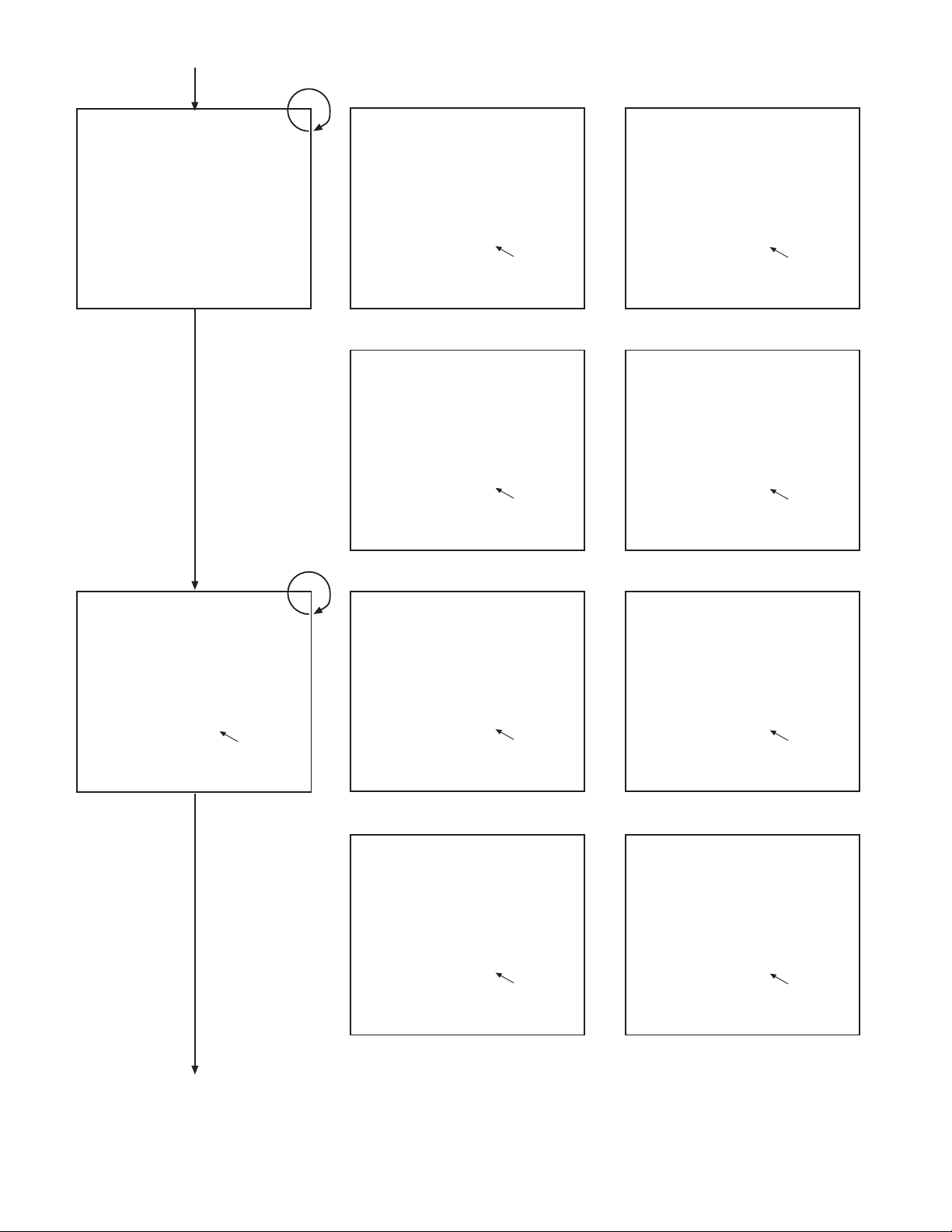
VIDEO
VIDEO
Your SHARP Projection TV has an O.P.C. (Optional Picture Control) function which will automatically adjust
picture settings to produce the highest quality picture possible.
When O.P.C. is highlighted, press SELECT to turn the O.P.C. on or off.
Use CURSOR G or H to select function.
Press SELECT to select the function setting. When the function has an Ò Ó in the box, it is ON.
Use CURSOR E to change COLOR TEMPERATURE or ASPECT RATIO setting. When the function shows a Ò Ò, it is selected.
Use CURSOR E to enter V. POSITION mode, then use CURSOR G or H to adjust V. POSITION.
Press EXIT to quit menu or CURSOR F to return to previous menu.
O.P.C. (Optional Picture Control)
When the O.P.C. function is on, the TVsÕ internal computer will perform the following:
1. Automatically monitor and adjust contrast depending on room lighting (sensor is located in the front panel) to produce a more
natural picture.
2. Automatically monitor and adjust color levels and maintain natural flesh tones.
3. Automatically compensate for weak or strong TV signals to produce a clear picture.
Turn the O.P.C. function off to control additional OTHER SETTINGS.
FLESH TONE
The FLESH TONE function automatically monitors and adjusts the color to maintain constant color levels even after a program or
channel changes. It also maintains natural flesh tones while preserving fidelity of background colors. (This function will automatically
set to on and cannot be turned off when the O.P.C. function is ON.) This function does not operate with a COMPONENT: Y-PBPRinput
signal.
NOISE REDUCTION
The NOISE REDUCTION function automatically reduces conspicuous noise in the picture without degrading picture quality.
(This function will automatically be set to on and cannot be turned off when the O.P.C. function is ON.)
COLOR TEMPERATURE
Set this to WARM for hotter colors with more red, or set to COOL for less intense colors with more blue.
ASPECT RATIO
Adjust this when viewing a COMPONENT: Y-PBPRinput signal.
16:9 - Screen changes to 16:9 aspect ratio. (gray bars visible on top and bottom of screen). HDTV signals are normally 16:9 aspect
ratio.
4:3 - Screen changes to 4:3 aspect ratio. (entire screen is filled with video). SDTV and NTSC signals are normally 4:3 aspect ratio.
V. POSITION
Adjust this when viewing a COMPONENT: Y-PBPRsignal. This feature is used to center an HDTV video signal between the top and
bottom gray bars. Adjustable range is -10 (video center is toward bottom of screen) to +10 (video center is toward top of screen).
OTHER
SETTINGS
MENU TO MENU BAR TO QUIT EXIT
MENU TO MENU BAR TO QUIT EXIT
MENU TO MENU BAR TO QUIT EXIT
CURSOR
100%
50%
50%
50%
PRESS SELECT TO
ACTIVATE/DEACTIVATE
FAV.
CURSOR
FAV.
CURSOR
SET UP CUSTOMIZE VIDEO AUDIO THEATER
SET UP CUSTOMIZE VIDEO AUDIO THEATER
VIDEO
OTHER SETTINGS
O.P.C.
FLESH TONE
NOISE REDUCTION
COLOR TEMPERATURE
COOL WARM
ASPECT RATIO
4:3 16:9
V. POSITION 0
OTHER SETTINGS
O.P.C.
FLESH TONE
NOISE REDUCTION
COLOR TEMPERATURE
COOL WARM
ASPECT RATIO
4:3 16:9
V. POSITION 0
1. PICTURE
2. BRIGHT
3. COLOR
4. TINT
5. SHARP
6. RESET
7. OTHER
SETTINGS
Page 22

22
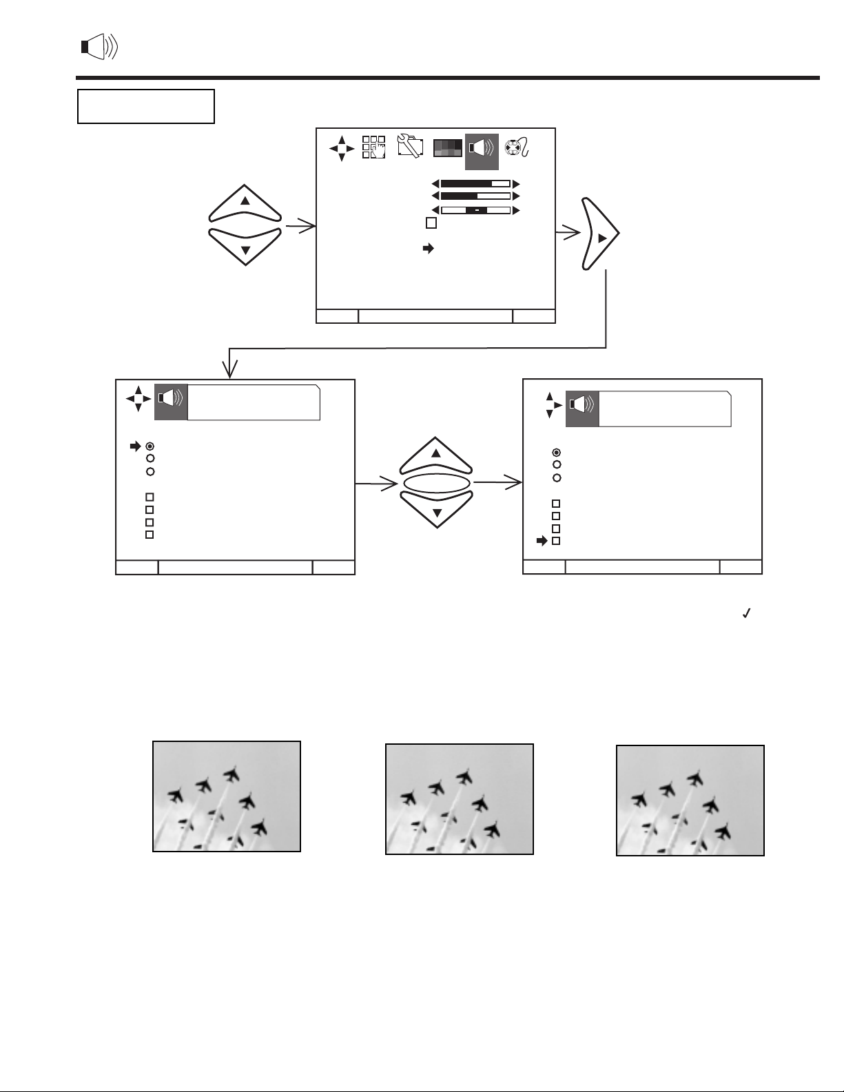
AUDIO
AUDIO
Select AUDIO to adjust the TV to your preference and to improve the sound quality.
AUDIO
This function controls the low frequency audio to all speakers.
Use CURSOR G or H to highlight the function to be adjusted.
Press CURSOR F or E to adjust the function.
When RESET is highlighted, press SELECT to reset audio settings to factory conditions.
Press EXIT to quit menu.
NOTE: If BASS is selected you are adjusting BASS. The additional menu items TREBLE and BALANCE can be selected and
adjusted in the same manner.
This function controls the high frequency audio to all speakers.
This function will control the left to right balance of the TV internal speakers and the AUDIO TO HI FI output.
When RESET is selected, press SELECT to return audio adjustments to factory preset conditions.
BASS
BALANCE
RESET
TREBLE
MENU TO MENU BAR TO QUIT EXIT
MENU TO MENU BAR TO QUIT EXIT
CURSOR
72%
50%
1. BASS
2. TREBLE
3. BALANCE
4. RESET
5. OTHER
SETTINGS
90%
50%
FAV.
FAV.
MENU
FAV.
CURSOR
SET UP CUSTOMIZE VIDEO AUDIO THEATER SET UP CUSTOMIZE VIDEO AUDIO THEATER
1. BASS
2. TREBLE
3. BALANCE
4. RESET
5. OTHER
SETTINGS
Use this function to improve the sound performance of your TV, depending on listening conditions.
OTHER SETTINGS
Page 23
23
AUDIO
AUDIO
Use OTHER SETTINGS to improve the sound performance of your TV, depending on listening conditions.
MTS MODE
Multi-Channel Television Sound will allow you to select STEREO (a stereo broadcast), MONO (monaural sound) used when receiving
a weak stereo broadcast or SAP (second audio program) which may be a secondary language, weather report, etc.
The sources received will be displayed at the top center edge of the TV. The source you select will be displayed above the sources
received. See the example below for each selection when both stereo and second audio are received (monaural is always received).
Press CURSOR G or H to highlight a function. Press SELECT to change the function setting. When the function has a Ò Ó in the box
it is ON, when it has a Ò Ò it is selected.
OTHER
SETTINGS
MENU TO MENU BAR TO QUIT EXIT
MENU TO MENU BAR TO QUIT EXIT
MENU TO MENU BAR TO QUIT EXIT
CURSOR
√
√
√
PRESS SELECT TO
ACTIVATE/DEACTIVATE
72%
50%
1. BASS
2. TREBLE
3. BALANCE
4. RESET
5. ADVANCED
SETTINGS
FAV.
SELECT
CURSOR
CURSOR
SET UP CUSTOMIZE VIDEO AUDIO THEATER
AUDIO
PRESS SELECT TO
ACTIVATE/DEACTIVATE
AUDIO
ADVANCED SETTINGS
STEREO
MONO
SECOND AUDIO PROGRAM
INTERNAL SPEAKERS
AUTO NOISE CANCEL
LOUDNESS
PERFECT VOLUME
ADVANCED SETTINGS
STEREO
MONO
SECOND AUDIO PROGRAM
INTERNAL SPEAKERS
AUTO NOISE CANCEL
LOUDNESS
PERFECT VOLUME
INTERNAL SPEAKERS
This function is useful if you prefer to use only speakers from a separate stereo system.
AUTO NOISE CANCEL
This function eliminates the noise between stations. If a channel is tuned and is noisy, this function will automatically eliminate the audio
for that channel.
LOUDNESS
This function will improve the quality of both low and high frequency sounds when listening at low volume levels.
CONSTANT VOLUME
This function will automatically adjust volume so each channel has the same average volume level.
ANT A 31
NEWS
10:00 PM
ANT A 31
NEWS
10:00 PM
STEREO SELECTED
SAP SELECTED
MONO SELECTED
STEREO
ST/SA
ANT A 31
NEWS
10:00 PM
SAP
ST/SA
MONO
Page 24

24
SERVICE ADJUSTMENTS
1. I2C ADJUSTMENT..............................................................................................................................................25
1-1. Memory Initialization (SDTV AND HDTV) ..............................................................................................25
1-2. Comb Filter Operation Check ................................................................................................................35
1-3. Audio Operation Check ..........................................................................................................................35
1-3-1. Tone Control Check......................................................................................................................35
1-3-2. Constant Volume Operation Check..............................................................................................35
1-3-3. SRS Check ..................................................................................................................................35
1-4. High Voltage Adjustment ........................................................................................................................36
2. FINAL ASSEMBLY ADJUSTMENT (Adjustment should be according to below order) ..............................36
2-1. Cut Off ....................................................................................................................................................36
2-2. DCU Phase Data Setting (Progressive and HD mode)..........................................................................36
2-3. Horizontal Position Adjustment (Coarse)................................................................................................37
2-4. Raster Tilt (Deflection Yoke)....................................................................................................................37
2-5. Beam Alignment......................................................................................................................................37
2-6. Raster Position........................................................................................................................................38
2-7. Vertical Size (Progressive and HD mode) ..............................................................................................38
2-8. Horizontal Size (Progressive and HD mode)..........................................................................................38
2-9. Beam Form ............................................................................................................................................39
2-10. Lens Focus..............................................................................................................................................39
2-11. Static Focus ............................................................................................................................................39
2-12. Digital Convergence (Progressive and HD mode) ..................................................................................42
2-13-1. Raster Position ..........................................................................................................................43
2-13-2. Convergence Point ....................................................................................................................44
2-13. Blue Defocus ..........................................................................................................................................45
2-14. White Balance ........................................................................................................................................45
2-15. Sub Brightness ........................................................................................................................................45
2-16. Horizontal Position (Progressive and HD mode)....................................................................................46
2-17. Scanning Area Check ................................................................................................................................
3. ADJUSTMENT POINT........................................................................................................................................47
3-1. CRT (R)(G)(B), Cabinet Locations..........................................................................................................47
3-2. Main Chassis (Signal P.W.B.) ................................................................................................................48
3-3. Main Chassis (Power/Deflection P.W.B.) ................................................................................................49
3-4. Power Supply P.W.B...............................................................................................................................50
3-5. CPT (R)(G)(B), Focus Pack, Control P.W.B. ..........................................................................................51
*IMPORTANT
For many of the above adjustments, it is necessary to have an HDTV (1080i) signal generator, SDTV (480P) signal
genrator, as well as the usual NTSC (480i) signal generator.
Sharp recognizes that few companies offer HDTV or SDTV signal generators and that the cost of these generators
is sometimes prohibited. For this reason, we suggest the use of a set-top-box for HDTV and SDTV adjustments.
Usually, there is a switch on the set-top-box which enables it to output HDTV (1080i) or SDTV (480P) signals even
with no input. In this case, the sync is automatically detected by the TV (at the Y-P
BPR
Inputs on the rear panel).
Page 25
25
1. I2C ADJUSTMENT
1.1 Memory Initialization
Adjustment Procedure
(1) Press and hold the INPUT key on Control Panel and then Power ON to access I2C adjustment mode.
(2) Receive signal on main picture. (NTSC, SDTV or HDTV).
Some menu pages have I2C adjustments for SDTV and HDTV. The set will automatically allow you to set
these items only when a SDTV or HDTV signal is input to the COMPONENT jacks on the back of the TV.
See table below.
(3) Check the OSD according to the I2C data on page 28~34, using CURSOR G, H on Remote Control.
All data should be exactly as stated on page 28~34 exept adjustable data (*).
*: Adjustable Data
Others: Fixed Data (be careful not to change)
(4) Press MENU key to exit I2C ADJUSTMENT mode.
NOTE: (1) If there is a different value than shown in table above, for fixed data, adjust it using CURSOR F, E
(only in this case).
(2) When exchanging microprocessor and TV is turned on for first time, it requires initialization of
Memory Initial of I2C adjustment menu.
SIGNAL ASPECT fH COLOR
HDTV 1080i 16:9 33.75kHz Y PBP
HDTV 720P 16:9 45kHz Y PBP
SDTV 480P 4:3 31.5kHz Y CBC
NTSC 480i 4:3 15.75kHz Y CBC
R
R
R
R
NTSC NTSC
Page 26
26
ANT A 10
ABCD
10:00PM
PIP ANT A 12
STEREO
ST/SA
SLEEP 0:15
SLEEP
TIMER
Audio
Broadcast
Audio Selected
Main Picture Source
CHANNEL ID
Time
Sub-Picture
Source
PIP
SURF/B
SURF/
BACK
Page 27
27
(5) HDTV: 1080i 16x9 (33.75kHz) 1080i 4x3 (33.75kHz)
16x9
1080i
33.75kHz
16x9
1080i
33.75kHz
Insertion panel to top and bottom.
810
Lines
1080
Lines
4x3
1080i
33.75kHz
1080
Lines
(6) HDTV: 1080i 16x9 (33.75kHz) 1080i 4x3 (33.75kHz)
16x9
1080i
33.75kHz
(7) HDTV: 720P 16x9 (45kHz) 480P 4x3 (31.5kHz)
16x9
720P
45kHz
16x9
480P
31.5kHz
Insertion panel to top and bottom.
360
Lines
480
Lines
4x3
480P
33.75kHz
480
Lines
(8) HDTV: 720P 16x9 (45kHz) 480P 4x3 (31.5kHz)
16x9
720P
45kHz
B. SURF/STROBE MODE NTSC 480P 4x3 (31.5kHz)
Main
Picture
480
Lines
360
Lines
SUB
SUB
SUB
Main
Picture
Sub
Picture
NTSC
Picture
Moving
Picture
480
Lines
360
Lines
STROBE
STROBE
STROBE
Page 28

28
I2C Parameter List
(1) Adjust Mode OSD
Press [POWER] + [INPUT] keys of front control panel.
*: ADJUSTABLE ITEM
EXIT I2C ADJUST MODE
POWER on/off.
ADJUST MODE
SUB BRT
SERVICE
DEF RESET
V/P RESET
3DYC RESET
FLEX RESET
DSP RESET
CCD RESET
FACT RESET
MEMORY INITIAL
l
l
l
l
l
l
l
l
l
l
SUB BRT 80
(OSD OFF)
Press key
Press
key
Select SERVICE
and Press key
ADJUST MODE
TA1300 315
H POSI 40
FLEX CONT
47 VD-POS 3F
UPD64081
DYGA 9
DCGA 6
VAPGA 5
VAPIN 0B
YHCOR 0
ADJUST MODE
TA1300 3375
H POSI 40
FLEX CONT
47 VD-POS 3F
UPD64081
DYGA 9
DCGA 6
VAPGA 5
VAPIN 0B
YHCOR 0
31.5kHz
Mode
33.75kHz
Mode
ADJUST MODE
TA1270-M
TINT (TV) 3C
TOFFO (TV) 00
TOFQ (TV) 00
SUB CNT 0F
SUB CLR 1B
ADJUST MODE
TA1270-S
TINT (TV) 3C
TOFFO (TV) 00
TOFQ (TV) 00
SUB CNT 0F
SUB CLR 1B
POWER+INPUT
A
CURSOR,MENU
Select SUB BRIGHT
and Press key
Page 29
29
MENU
FLEX CONT NTSC
39 HHPF1 00
41 V-CRG 00
42 H-CRG 00
43 V-ENH 00
44 H-ENH 00
96 YVHENH 0B
100 CVHENH 12
FLEX CONT 480i
39 HHPF1 00
41 V-CRG 00
42 H-CRG 00
43 V-ENH 02
44 H-ENH 00
96 YVHENH 0B
100 CVHENH 12
FLEX CONT 480P
39 HHPF1 00
41 V-CRG 00
42 H-CRG 00
43 V-ENH 02
44 H-ENH 00
96 YVHENH 0B
100 CVHENH 12
480i
Mode
480P
Mode
FLEX CONT 1080i
39 HHPF1 00
41 V-CRG 00
42 H-CRG 00
43 V-ENH 00
44 H-ENH 00
96 YVHENH 00
100 CVHENH 12
FLEX CONT 720P
39 HHPF1 00
41 V-CRG 00
42 H-CRG 00
43 V-ENH 02
44 H-ENH 00
96 YVHENH 1B
100 CVHENH 12
1080i
Mode
720P
Mode
CURSOR,MENU
FLEX CONT NTSC
71 YV-ENH 00
79 CV-ENH 00
87 YH-ENH 07
94 CH-ENH 0F
66 YV-DSB 00
75 CV-DSB 00
82 YH-DSB 00
90 CH-DSB 00
68 YV-CLP 00
84 YH-CLP 00
FLEX CONT 480i
71 YV-ENH 00
79 CV-ENH 00
87 YH-ENH 07
94 CH-ENH 0F
66 YV-DSB 00
75 CV-DSB 00
82 YH-DSB 00
90 CH-DSB 00
68 YV-CLP 00
84 YH-CLP 00
FLEX CONT 480P
71 YV-ENH 00
79 CV-ENH 00
87 YH-ENH 07
94 CH-ENH 0F
66 YV-DSB 00
75 CV-DSB 00
82 YH-DSB 00
90 CH-DSB 00
68 YV-CLP 00
84 YH-CLP 00
480i
Mode
480P
Mode
G , H
NTSC
Mode
FLEX CONT 1080i
71 YV-ENH 00
79 CV-ENH 00
87 YH-ENH 00
94 CH-ENH 0F
66 YV-DSB 00
75 CV-DSB 00
82 YH-DSB 00
90 CH-DSB 00
68 YV-CLP 00
84 YH-CLP 00
FLEX CONT 720P
71 YV-ENH 00
79 CV-ENH 00
87 YH-ENH 07
94 CH-ENH 0F
66 YV-DSB 00
75 CV-DSB 00
82 YH-DSB 00
90 CH-DSB 00
68 YV-CLP 00
84 YH-CLP 00
1080i
Mode
720P
Mode
G , H
Page 30

30
MENU
FLEX CONT NTSC
97 YV-NLP 00
98 YH-NLP 0A
Y-LMT FF
83 YH-FRQ 00
91 CH-FRQ 02
70 YV-LTI 00
78 CV-CTI 00
86 YH-LTI 01
93 CH-CTI 01
FLEX CONT 480i
97 YV-NLP 00
98 YH-NLP 0A
Y-LMT FF
83 YH-FRQ 00
91 CH-FRQ 02
70 YV-LTI 00
78 CV-CTI 00
86 YH-LTI 01
93 CH-CTI 01
FLEX CONT 480P
97 YV-NLP 00
98 YH-NLP 0A
Y-LMT FF
83 YH-FRQ 00
91 CH-FRQ 02
70 YV-LTI 00
78 CV-CTI 00
86 YH-LTI 01
93 CH-CTI 01
480i
Mode
480P
Mode
FLEX CONT 1080i
97 YV-NLP 00
98 YH-NLP 0A
Y-LMT FF
83 YH-FRQ 00
91 CH-FRQ 02
70 YV-LTI 00
78 CV-CTI 00
86 YH-LTI 00
93 CH-CTI 01
FLEX CONT 720P
97 YV-NLP 00
98 YH-NLP 0A
Y-LMT FF
83 YH-FRQ 00
91 CH-FRQ 02
70 YV-LTI 00
78 CV-CTI 00
86 YH-LTI 01
93 CH-CTI 01
1080i
Mode
720P
Mode
CURSOR,MENU
FLEX CONT NTSC
69 YVDSBC 00
77 CVDSBC 00
85 YHDSBC 00
92 CHDSBC 00
95 Y-CRG 00
99 C-CRG 00
64 YNR-IN 04
73 CNR-IN 04
80 YNRPAS 00
88 CNRPAS 02
FLEX CONT 480i
69 YVDSBC 00
77 CVDSBC 00
85 YHDSBC 00
92 CHDSBC 00
95 Y-CRG 00
99 C-CRG 00
64 YNR-IN 04
73 CNR-IN 04
80 YNRPAS 00
88 CNRPAS 02
FLEX CONT 480P
69 YVDSBC 00
77 CVDSBC 00
85 YHDSBC 00
92 CHDSBC 00
95 Y-CRG 00
99 C-CRG 00
64 YNR-IN 04
73 CNR-IN 04
80 YNRPAS 00
88 CNRPAS 02
480i
Mode
480P
Mode
G , H
NTSC
Mode
FLEX CONT 1080i
69 YVDSBC 00
77 CVDSBC 00
85 YHDSBC 00
92 CHDSBC 00
95 Y-CRG 00
99 C-CRG 00
64 YNR-IN 04
73 CNR-IN 04
80 YNRPAS 00
88 CNRPAS 02
FLEX CONT 720P
69 YVDSBC 00
77 CVDSBC 00
85 YHDSBC 00
92 CHDSBC 00
95 Y-CRG 00
99 C-CRG 00
64 YNR-IN 04
73 CNR-IN 04
80 YNRPAS 00
88 CNRPAS 02
1080i
Mode
720P
Mode
G , H
NTSC
Mode
101
101
101
101 101
Page 31

31
MENU
FLEX CONT NTSC
65 YNRRDC 00
74 CNRRDC 00
67 YNR-DC 00
76 CNR-DC 00
81 YNR-0 00
89 CNR-0 00
45 CB-BLK 07
46 CR-BLK 07
27 FRMBRT 60
102 CLPOUT 7F
FLEX CONT 480i
65 YNRRDC 00
74 CNRRDC 00
67 YNR-DC 00
76 CNR-DC 00
81 YNR-0 00
89 CNR-0 00
45 CB-BLK 07
46 CR-BLK 07
27 FRMBRT 60
102 CLPOUT 7F
FLEX CONT 480P
65 YNRRDC 00
74 CNRRDC 00
67 YNR-DC 00
76 CNR-DC 00
81 YNR-0 00
89 CNR-0 00
45 CB-BLK 07
46 CR-BLK 07
27 FRMBRT 60
102 CLPOUT 7F
480i
Mode
480P
Mode
FLEX CONT 1080i
65 YNRRDC 00
74 CNRRDC 00
67 YNR-DC 00
76 CNR-DC 00
81 YNR-0 00
89 CNR-0 00
45 CB-BLK 07
46 CR-BLK 07
27 FRMBRT 60
102 CLPOUT 7F
FLEX CONT 720P
65 YNRRDC 00
74 CNRRDC 00
67 YNR-DC 00
76 CNR-DC 00
81 YNR-0 00
89 CNR-0 00
45 CB-BLK 07
46 CR-BLK 07
27 FRMBRT 60
102 CLPOUT 7F
1080i
Mode
720P
Mode
FLEX CONT NTSC
10 MPLL-S 0F
17 SPLL-S 0F
12 MPLL-E 0F
19 SPLL-E 0F
11 MVW-PH 05
18 SVW-PH 05
14 MHS-HP 0F
21 SHS-HP 0F
13 MY-CLP 03
20 SY-CLP 03
FLEX CONT 480i
10 MPLL-S 0F
17 SPLL-S 0F
12 MPLL-E 0F
19 SPLL-E 0F
11 MVW-PH 05
18 SVW-PH 05
14 MHS-HP 0F
21 SHS-HP 0F
13 MY-CLP 03
20 SY-CLP 03
FLEX CONT 480P
10 MPLL-S 0F
17 SPLL-S 0F
12 MPLL-E 0F
19 SPLL-E 0F
11 MVW-PH 05
18 SVW-PH 05
14 MHS-HP 0F
21 SHS-HP 0F
13 MY-CLP 03
20 SY-CLP 03
480i
Mode
480P
Mode
G , H
NTSC
Mode
FLEX CONT 1080i
10 MPLL-S 0F
17 SPLL-S 0F
12 MPLL-E 0F
19 SPLL-E 0F
11 MVW-PH 05
18 SVW-PH 05
14 MHS-HP 0F
21 SHS-HP 0F
13 MY-CLP 03
20 SY-CLP 03
FLEX CONT 720P
10 MPLL-S 0F
17 SPLL-S 0F
12 MPLL-E 0F
19 SPLL-E 0F
11 MVW-PH 05
18 SVW-PH 05
14 MHS-HP 0F
21 SHS-HP 0F
13 MY-CLP 03
20 SY-CLP 03
1080i
Mode
720P
Mode
G , H
NTSC
Mode
Page 32

32
MENU
FLEX CONT NTSC
23 V-POS 3F
24 V-SIZ 7F
50 HD-POS 3F
48 VBLK-T 7F
49 VBLK-B 7F
51 HBLK-R 7F
52 HBLK-L 7F
40 READ-F 10
FLEX CONT 480i
23 V-POS 3F
24 V-SIZ 7F
50 HD-POS 3F
48 VBLK-T 7F
49 VBLK-B 7F
51 HBLK-R 7F
52 HBLK-L 7F
40 READ-F 10
FLEX CONT 480P
23 V-POS 3F
24 V-SIZ 7F
50 HD-POS 3F
48 VBLK-T 7F
49 VBLK-B 7F
51 HBLK-R 7F
52 HBLK-L 7F
40 READ-F 10
480i
Mode
480P
Mode
FLEX CONT 1080i
23 V-POS 3F
24 V-SIZ 7F
50 HD-POS 3F
48 VBLK-T 7F
49 VBLK-B 7F
51 HBLK-R 7F
52 HBLK-L 7F
40 READ-F 0E
FLEX CONT 720P
23 V-POS 1F
24 V-SIZ 7F
50 HD-POS 3F
48 VBLK-T 7F
49 VBLK-B 7F
51 HBLK-R 7F
52 HBLK-L 7F
40 READ-F 0F
1080i
Mode
720P
Mode
FLEX CONT NTSC
35 FRMTOP-2 07
FRMTOP-L 07
36 FRMBTM-2 07
FRMBTM-L 07
37 FRMRGT 07
38 FRMLFT 07
59 BS-TOP 07
60 BS-BTM 07
61 BS-RGT 07
62 BS-LFT 07
FLEX CONT 480i
35 FRMTOP-2 07
FRMTOP-L 07
36 FRMBTM-2 07
FRMBTM-L 07
37 FRMRGT 07
38 FRMLFT 07
59 BS-TOP 07
60 BS-BTM 07
61 BS-RGT 07
62 BS-LFT 07
FLEX CONT 480P
35 FRMTOP-2 07
FRMTOP-L 07
36 FRMBTM-2 07
FRMBTM-L 07
37 FRMRGT 07
38 FRMLFT 07
59 BS-TOP 07
60 BS-BTM 07
61 BS-RGT 07
62 BS-LFT 07
480i
Mode
480P
Mode
G , H
NTSC
Mode
FLEX CONT 1080i
35 FRMTOP-2 07
FRMTOP-L 07
36 FRMBTM-2 07
FRMBTM-L 07
37 FRMRGT 07
38 FRMLFT 07
59 BS-TOP 07
60 BS-BTM 07
61 BS-RGT 07
62 BS-LFT 07
FLEX CONT 720P
35 FRMTOP-2 07
FRMTOP-L 07
36 FRMBTM-2 07
FRMBTM-L 07
37 FRMRGT 07
38 FRMLFT 07
59 BS-TOP 07
60 BS-BTM 07
61 BS-RGT 07
62 BS-LFT 07
1080i
Mode
720P
Mode
G , H
NTSC
Mode
SWX
only
SWX
only
SWX
only
SWX
only
SWX
only
Page 33

33
MENU
FLEX CONT
120 TV/CINE 01
121 T/C DET 07
122 T/C UNL 01
123 T/C LCK 03
126 T/C ARE 05
127 T/C CBR 07
128 T/C YBR 07
TA1298 NTSC
SHARP 0C
APACON 06
YNR 00
TA1298 480i
SHARP 0A
APACON 06
YNR 00
TA1298 480P
SHARP 07
APACON 05
YNR 00
SDTV
Mode
HDTV
Mode
G , H
NTSC
Mode
G , H
Page 34

34
MENU
TA1298 NTSC
COLOR 40
TINT 45
R-Y PH 02
R/B GA 01
G-Y PH 00
G/B GA 00
COLOR SYSTEM 00
TA1298 SDTV
COLOR 4F
TINT 3B
R-Y PH 02
R/B GA 02
G-Y PH 01
G/B GA 00
COLOR SYSTEM 01
TA1298 HDTV
COLOR 40
TINT 43
R-Y PH 00
R/B GA 02
G-Y PH 02
G/B GA 00
COLOR SYSTEM 01
SDTV
Mode
HDTV
Mode
NTSC
Mode
TA1298
RGB BRT 50
RGB CNT 50
G DRV (W) 39
B DRV (W) 2D
SUB CLR 10
SUB CNT 1G
VSM PH 05
VSM GA 00
OS ACL 01
RGB ACL 00
COLOR TEMP
WARM MODE
Center
Adjust
TA1298
CLR G 00
CLT 00
YOUT G 00
Y G PNT 00
S TRK 00
RGB G 00
DC PNT 00
DC RAT 00
DC LMT 00
CH U/D, AVX
G , H
G , H
TA1298
BSP 03
APL/BS 00
B COR 01
B GA 00
B DET 00
DABL PN 00
DABL GA 07
ABL PN 07
ABL GA 05
CH U/D, AVX
G , H
MENU
TA1298 NTSC
COLOR 40
TINT 45
R-Y PH 02
R/B GA 01
G-Y PH 00
G/B GA 00
COLOR SYSTEM 00
TA1298 SDTV
COLOR 4F
TINT 3B
R-Y PH 02
R/B GA 02
G-Y PH 01
G/B GA 00
COLOR SYSTEM 01
SDTV
Mode
NTSC
Mode
TA1298
Center
Adjust
TA1298
CH U/D,
G , H
Page 35

35
1.2 Comb filter operation check
Adjustment preparation
(1) Receive the color bar signal at the regular
tuning point.
(2) Set the CONTRAST control to MAX and the
other controls to center.
(3) Set the O.P.C. to OFF.
Adjustment procedure
(1) Check that between the color bars there are not
line dots every second color bar as shown in the
drawing.
A
A A
B
SP05
A No Dots
B No Dots
Check and line dots.
B
A
1.3 AUDIO OPERATION CHECK
1.3.1 TONE CONTROL CHECK
Preparation for adjustment
(1) Input an audio signal of 250Hz and 3Khz in
order with level of 150mVrms to the L/mono
audio input.
(2) Set the Volume to around the center.
(3) Set SRS SURROUND to OFF.
(4) Set LOUDNESS to OFF.
(5) Set INTERNAL SPEAKER to ON.
Adjustment Procedure
(1) Select BASS mode and check that the audio
output level of the speakers changes to
emphasized or supporessed when adjust to
max. or min. of the adjustment mode.
(2) Select TREBLE mode and check that the
audio output level of the speakers changes
by emphasized or suppressed when adjust to
max. or min. of the adjustment mode.
(3) Select BALANCE mode and check that the
audio output changes right or left when adjust
to right or left of the adjustment mode.
1.3.2 CONSTANT VOLUME OPERATION CHECK
Preparation for adjustment
CONSTANT VOLUME mode should be ON.
Procedure
(1) Input 100mVrms, 200mVrms, 300mVrms and
400mVrms of 1KHz sound signal to L/MONO
terminal.
(2) Check same level sound is output from SP
when 200mVrms, 300mVrms and 400mVrms
of 1KHz sound signal is input.
1.3.3 SRS CHECK
Preparation for adjustment
(1) Set the AUDIO SETTINGS as follows:
BALANCE:CENTER BASS and
TREBLE:CENTER, INTERNAL
SPEAKER:ON, LOUDNESS:OFF,
CONSTANT VOL:OFF.
(2) Input the signal to the VIDEO INPUT (R)
terminal as follows.
Adjustment procedure
(1) Check that the following waveform is output
at HiFi output (L).
(2) Check that the following waveform is output
at HiFi (R) output.
1Vpp
R ch: 400Hz 1Vpp
L ch: no signal
0
(a) SRS : OFF
1.4Vpp ±0.05
(b) SRS : ON
0
1.9Vpp ±0.05
(a) SRS : OFF
0
0.3Vpp ±0.05
(a) SRS : ON
0
Page 36

36
Important: High Voltage adjustment should
NOT be adjusted in field. This is
adjusted at factory using precise
loads and should NOT be
readjusted.
1.4 High Voltage Adjustment (should NOT be
readjusted in field).
Adjustment preparation
(1) Connect High Voltage meter to FBT High Voltage
output. Connect GND of High Voltage meter to CPT
GND or FBT GND.
(2) Check that High Voltage adjustment VR (RH44) is
set to mechanical center(located behind FBT on
DEFLECTION PWB).
(3) Receive circle pattern signal.
(4) VIDEO control should be reset.
Adjustment procedure
(1) Adjust High Voltage to following spec. by turning VR
RH44 clockwise slowly. (This should never need
adjustment).
ADJ. SPEC = 30.0kV +/-0. 5kV
(2) After adjustment, fix VR RH44 by Silicone glue
(KE40RTV).
2. FINAL ASSEMBLY ADJUSTMENT
2.1 Cut Off Adjustment
Adjustment preparation
(1) Set R and G drive VR’s on CPT P.W.B. to center .
(2) Adjust screen VR’s on Focus Pack fully
counterclockwise.
(3) Adjust Focus VR’s on Focus Pack fully
clockwise.
(4) Set video conditions to factory preset.
(5) The vertical incident illumination on the screen
should be 20 lux or less (room should be dark).
!
K
Adjustment procedure
(1) Press and hold INPUT key on the control panel
and then POWER ON to access I
2
C adjustment
mode.
(2) Choose “SERVICE” item from I
2
C adjustment
menu by pressing E key.
(3) Screen VR should be turned clockwise gradually
and set so that retrace line begins to appear.
(4) Return to “NORMAL” mode by CURSOR E key
again.
(5) Adjust Focus VR’s so that focus is even all
around screen.
2.2 DCU Phase Data Setting
Adjustment preparation
(1) Cut off adjustment should finished.
(2) Set video conditions to factory preset.
Adjustment procedure
(1) Receive any NTSC signal.
(2) Push “SERVICE ONLY” switch on
DEFLECTION PWB. (Enter DCU ADJ. mode).
(3) Push HELP key on R/C. (Green cross hatch is
displayed).
Then push EXIT key on R/C. (Character pattern
is displayed. This is the PHASE setting mode).
(4) Set PH-H phase data as shown below by using
4 and 6 key on Remote Control (RC).
(5) Set PH-V phase data as shown below by using
2 and 5 key on R/C.
(6) Set CR-H phase data as shown below by using
CURSOR F and E key on R/C.
(7) Set CR-V phase data as shown below by using
CURSOR G and H key on R/C.
(8) Push HELP key on R/C to exit from the PHASE
mode.
(9) Push PIP MOVE key 2 times on R/C to write the
phase data to memory.
(10) When Green dots are displayed, push MUTE
key to return to DCU ADJ. mode.
(1 1)Push “SERVICE ONLY” switch to return to RF or
VIDEO mode.
(12)Receive any HD signal (Set to video: 1 or 2
mode with HD input to component jacks).
(13)Repeat steps (2) ˜(11) above.
PROGRESSIVE MODE
TH01
HD MODE
HD MODE
PROGRESSIVE MODE
PHASE MODE
PH-H: BB
PH-V: 0C
CR-H: 4C
CR-V: 00
PHASE MODE
PH-H: BB
PH-V: 07
CR-H: 4C
CR-V: 0C
(FBT)
High Voltage Adjustment VR.
RH44
T702
DEFLECTION PWB.
CONV.
HEATSIN
Page 37

37
2.3 HOR. POSITION ADJUSTMENT (Coarse)
Adjustment preparation
(1) DCU PHASE DATA SETTING should be
finished.
Adjustment procedure
(1) Receive circle pattern (03ch.)
(2) Push SERVICE ONLY switch then DCU
crosshatch is displayed. Mark the DCU
crosshatch center position using your finger tip.
(3) Push SERVICE ONLY switch again to exit from
the DCU crosshatch.
(4) Go to I
2
C ADJ. mode.
(5) Choose H. POSI item by using R/C MENU (or
up/down cursor) key. Adjust horizontal position
to match the circle center to DCU crosshatch
center (marked by your finger).
(6) Exit from I
2
C menu.
(1) Receive 1080I (fH=33.75KHz) circle pattern
signal. (Input to component video terminal.)
(2) Repeat above steps (2)~(6).
2.4 Raster Tilt adjustment (Deflection yoke)
Adjustment preparation
(1) The set can face east or west.
(2) Input the single cross test signal.
(3) Set video conditions to factory preset.
(4) The lens focus and horzontal position
adjustment should have been coarse adjusted.
(5) The electric focus should have been coarse
adjusted.
(6) The digital convergence RAM should be cleared
(uncorrected state). With the TV set off, press
and hold the service switch located on the
Power/Deflection PWB and then press the
power button.
(7) Start adjustment 20 minutes or more after TV is
turned on.
Adjustment procedure
(1) Apply covers to the R and B lenses and project
only green light.
(2) Turn the G deflection yoke and adjust the
vertical raster inclination.
(3) Then, remove the cover of R or B lens and
project red or blue light and green light together
on screen.
1
, 2≤±2mm
1
≤ ±2 m m
Notes: (1) If internal cross-hatch does not appear after
clearing RAM data, press service switch
again, on POWER/DEFLECTION PWB.
(2) To restore old RAM data, turn TV off and on.
CROSSHATCH (GREEN)
2
(4) Receive cross-hatch signal. (Use of internal
cross-hatch signals allowed.)
Adjustment procedure
(1) Green (G) tube beam alignment adjustment.
Short-circuit 2P subminiature connector plug
pins of Red (R) and Blue (B) on the CPT boards
and project only Green (G) light or you may
cover the R and B lens.
(2) Put Green (G) tube beam alignment magnet to
the cancel state as shown below.
(3) Turn the Green (G) static focus (Focus Pack)
counterclockwise all the way and make sure of
position of cross-hatch center on screen. (Halo
state.)
(4) Turn the Green (G) static focus (Focus Pack)
clockwise all the way. (Blooming state.)
(5) Turn two magnets forming alignment magnet in
any desired direction and move cross-hatch
center to position found in (3).
(6) If image position does not shift when Green (G)
static focus (Focus Pack) is turned. Green (G)
beam alignment has been completed.
(7) If image position shifts when Green (G) static
focus (Focus Pack) is turned, repeat (2)-(6).
(8) Conduct beam alignment for red (R) and Blue
(B) focus: Focus Pack UFPK.
(9) Upon completion of adjustment, fix beam
alignment magnets with white paint.
2.5 Beam alignment
Adjustment preparation
(1) Adjust at least 30 minutes after turning on power
switch.
(2) Raster tilt should be completed. Raster position,
horizontal and vertical size, and optical focus
adjustment should be coarse adjusted.
(3) Set video conditions to factory preset.
(4) Turn the deflection yoke of R or B and set so that the
inclination of R or B light with respect to the green
light is as shown below on the top and bottom sides.
(5) After raster inclination adjustment, fixing screw of DY
should be screwed with 12±2kg-cm torque.
Circle center
DCU crosshatch center
DCU crosshatch
Circle pattern
HD MODE
Page 38

38
Notes: (1) Only adjust the vertical size for
progressive mode (NTSC).
Because both modes (NTSC and
HD) have the same vertical
freuency.
(2) If internal cross-hatch does not
appear after clearing RAM data,
press service switch again (on
POWER/DEFLECTION PWB).
(3) To restore old RAM data, turn TV
off and on.
=
PROGRESSIVE
MODE
50NP4 650
60NP4 770
Tolerance: w 5mm Unit:mm
2.7 Vertical size adjustment
Adjustment preparation
(1) The set can face east or west.
(2) Set video conditions to factory preset.
(3) Horizontal size adjustment should be finished.
(4) Static focus adjustment should be finished.
(5) Start adjustment after TV is turned on for 20
minutes or more.
Adjustment procedure
(1) Receive any NTSC signal.
(2) Press and hold the SERVICE ONLY SW on
DEFLECTION PWB to display DCU crosshatch
with convergence data cleared.
(3) Adjust V. SIZE as following by using R630.
(4) After adjustment, press SERVICE ONLY switch
to exit from DCU crosshatch.
PROGRESSIVE MODE
(RED) (BLUE)
50NP4 15 25
50NP4 15 25
Tolerance: w 2mm
1
2
2.8 Horizontal size adjustment
Adjustment preparation
(1) The set can face east or west.
(2) Set video conditions to factory preset.
(3) BEAM FORM adjustment should be finished.
(4) Convergence should not be corrected.
(5) Start adjustment after TV is turned on for 20
minutes or more.
Adjustment procedure
(1) Receive any NTSC signal.
(2) Press and hold the SERVICE ONLY SW on
DEFLECTION PWB to display DCU cross-hatch
with Convergence data cleared.
(3) Convergence should not be adjusted.
(4) Adjust H. SIZE by using R683.
(5) After adjustment, press SERVICE ONLY SW to
exit from DCU cross-hatch.
(1) Input 1080I (fH=33. 75kHz) component signal to
VIDEO 2.
(2) Press and hold the SERVICE ONLY SW on
DEFLECTION PWB to display DCU cross-hatch
with convergence data cleared.
(3) Adjust H. SIZE using R686.
(4) After adjustment, press SERVICE ONLY SW to
exit from DCU crosshatch.
H. SIZE SPECIFICATION
PROGRESSIVE MODE
HD MODE
=
PROGRESSIVE
MODE
HD
MODE
50NP4 995 995
60NP4 1190 1190
Tolerance: w 5mm Unit:mm
Geometric
center of the
screen
R
B
(2) Upon completion of adjustment, fix beam
alignment magnets with white paint.
NOTES: (1) If internal cross-hatch does not appear
after clearing RAM data, press service
switch again.
(2) To restore old RAM data, turn TV off and
on.
12
2.6 Raster position adjustment
Adjustment preparation
(1) The set can face east or west.
(2) Receive the DCU cross-hatch signal.
(3) Set video conditions to factory preset.
(4) Static Focus adjustment should be finished.
(5) The digital convergence RAM should be cleared
(uncorrected state). With the TV set off, press
and hold the service switch located on the
Power/Deflection PWB and then press the
power button.
(6) Start adjustment 20 minutes or more after TV is
turned on.
Adjustment procedure
(1) Turn the centering magnets for red, green, and
blue to satisfy the condition below. The red and
blue horizontal lines should match with green.
V. SIZE SPECIFICATION
Page 39

39
Notes: (1) Progressive mode should be adjusted
before HD mode.
(2) If internal cross-hatch does not appear after
clearing RAM data, press service switch
again.
(3) To restore old RAM data, turn TV off and on.
TRUE CIRCLE DEGREE: a/b
SPECIFICATION: 0.9-1.1
PRT SURFACE SIDE
4-POLE BEAM
SHAPE CORRECTION
MAGNET
2-POLE BEAM
ALIGNMENT
MAGNET
ZERO FIELD
SPACER (NO
ADJUSTMENT)
b
a
2.9 Beam form adjustment
Adjustment preparation
(1) The beam alignment should have been
completed.
(2) The raster tilt, centering, horizontal/
vertical size, scanning area check, and raster
distortion should have been completed.
(3) Set video conditions to factory preset.
(4) Input the dot signal.
Adjustment procedure
(1) Green PRT beam shape adjustment. Short-
circuit 2P sub-mini connectors on Red and Blue
CPT P.W.B.s to project only the Green beam.
(2) Turn the green static focus VR, on the Focus
Pack, fully clockwise. (Blooming)
(3) Make the dot at the screen center a true circle
using the 4-pole magnet as shown below.
(4) Also adjust the Red and Blue PRT beam shapes
according to the steps (1) to (3).
(5) After the adjustment has been completed, return
R, G and B static VRs to the just focus point.
(6) After completed, fix beam form magnet with
white paint.
TRUE CIRCLE SPECIFICATION
2.10 LENS FOCUS ADJUSTMENT
Adjustment preparation
(1) The orientation of PTV set is arbitrary, west,
east, north and south.
(2) Centering DY inclination should have been
adjusted.
(3) Electrical focus adjustment should have been
completed.
(4) Drive VR location dajustment should have been
completed. (Red : 12 OÕclock, Green : 1~2
OÕclock).
(5) Receive the cross-hatch pattern signal.
(6) Refer to set below.
CONTRAST : HALF of full scale.
BRIGHTNESS : minimum
Adjustment procedure
(1) Loosen the fixing screww or wing nut on the lens
cylinder so that the lens cylinder can be turned.
(Be careful not to loosen too much). After
completing steps (4), (5), (6) below, tighten the
fixing scres or wing nuts for each lens with a
torque of 1.18N.m (12Kgf cm) ~ 1.67N.m (17Kgf
cm). (Be careful the lens cylinder does not turn
after having tightened the screw or wing nuts. If
it is tightened too much, lens may tilt or screw
may break.)
(2) Apply covers to each color of R, G and B lenses.
And project a single color on the screen and
adjust in sequence. (The adjustment order of R,
G and B is only an example.)
(3) If the lens adjustment knob is turned clockwise
viewed from the front, the color Aberration
change as follows.
(NOTE 1)
Fixing Screw
(NOTE 2)
Wing Nut
TYPE 1 TYPE 2
Lens Sass
Lens Sass
Color
Aberration
Cross-Hatch
Change of Color Aberration
Short focus Long focus
RED LENS Orange Scarlet
GREEN LENS Blue Red
BLUE LENS Purple Green
Page 40

40
(4) In case of G lens. Set to the point where the
chromatic aberration switches from blue to red.
If the chromatic aberration appearing all over
the screen is not the same, observe the vertical
bright line and adjust lens focus as specified in
table below. When the red chromtic aberration
appearing at both sides of the bright line is not
equal, observe the side with larger chromatic
aberration when adjusting.
OPTICAL FOCUSING ADJUSTMENT GREEN
Change the signal to the circle pattern and fine
adjust. Observe the corner part of the screen,
especially observe number in the small circle
shen adjusting. If the focus performance at the
screen center exceeds the lower limit, it is
accpetable.
0
1
L1
L2
CHASSIS SP05 (D78)
SCREEN SIZE 60Ó 50Ó
L1 and L2
(PITCHES from CENTER) 3.0 3.0
BETWEEN
L1&L2 * *
COLOR * *
ABERRATION I 3mm MAX 3mm MAX
** **
O 3mm MAX 3mm MAX
(NOTE) * Slightly reddish or no color
** Slightly bluish or no color
Small circle of circle pattern
NOTES: 1. Since the G light is very important for picture
quality and performance, pay special
attention in its adjustment.
2. Be careful not to touch the lens with your
fingers when adjusting.
(5) In case of R lens. Set the position where the
chromatic aberration changes from red to
crimson. As shown below, observe the vertical
bright line and adjust lens focus where the
crimson or red chromatic aberration slightly
appears inside and crimson or red outside
(reference value : 1~3mm) at the point specified
in table below. Change the signal and fineadjust in the same way as the G lens.
OPTICAL FOCUSING ADJUSTMENT RED
(6) In case of B lens. Set the position where the
chromatic aberration changes from purple to
green. As shown below, observe the vertical
bright line and adjust lens focus where the
purple or green chrmoatic aberration slightly
appears inside and purple or green outside
(reference value : 1~3mm) at the point specified
in table below. Change the signal and fineadjust in the same way as the G lens.
0
1
L
CHASSIS SP05 (D78)
SCREEN SIZE 60Ó 50Ó
L1 and L2
(PITCHES from CENTER) 3.0 3.0
BETWEEN
L1&L2 ** **
COLOR ** **
ABERRATION I 3mm MAX 3mm MAX
**
O 3mm MAX 3mm MAX
(NOTE) * Slightly reddish or no color
** Slightly bluish or no color
NOTE: Setting the center between Red and crimson is
optimum.
1
O
L
NOTE: Setting the center between purple and crimson is
optimum.
Page 41

41
Adjustment Procedure
(7) After all colors have been adjusted, display all
colors with the cross-hatch pattern signal and
compare the focus (optical focus) performance
with the llimit sample set.
(8) Then, select the circle pattern signal and
compare the focus (optical focus) performaces
of each color and all colors together with the
limit sample set.
(9) If the focus performance is worse than the limit
sample set, re-adjust step (1) to (6).
2.11 STATIC FOCUS ADJUSTMENT
Adjustment preparation
(1) LENS FOCUS adjustment should be finished.
(2) Contrast : MAX
Brightness : Center.
(3) Receive the circle pattern signal.
(4) Apply covers to the lens of the colors you are
not adjusting and project only one color on the
screen.
Adjustment procedure
(1) Red and blue static focus adjustment. Adjust
the static focus VR on Focus pack (UFPK) so
that the center of circle pattern is the most clear.
Check that the focus does not get
conspicuously worse at the edges of the circle
pattern signal or cross-hatch signal.
(2) Green static focus adjustment. Adjust the static
focus VR on Focus pack (UFPK) (for green) so
that the center of circle pattern is the most clear.
Check that the focus does not get
conspicuously worse at the checking point, the
periphery of circle pattern cross-hatch signal.
NOTE: Checking point for the periphery of picture.
Checking point
Page 42

42
762
1017
97
41
83.8
5.8
UNIT: mm
H.SIZE: 995
48.6
83.8
5.8
97
97
97
97
97
41
48.6
762
1017
108.5
1.4
83.8
5.8
UNIT: mm
H.SIZE: 995
54
108.5
1.4
54
15 25
83.8
5.8
V.SIZE: 650
914
1219
116.6
49.2
100.4
7.3
UNIT: mm
H.SIZE: 1190
58.2
100.4
7.3
49.2
58.2
914
1219
130.2
1.6
100.4
7.3
UNIT: mm
H.SIZE: 1190
65.1
130.2
1.6
65.1
15 25
100.4
7.3
V.SIZE: 770
116.6
116.6
116.6
116.6
116.6
50 DIGITAL COVERGENCE CROSSHATCH
Progressive Mode
HD mode
Progressive Mode
HD mode
60 DIGITAL COVERGENCE CROSSHATCH
Page 43

43
Note: If only minor adjustments to convergence are
needed, the jig screen is not necessary. Use
digital data stored in memory and one color as a
reference (red, green, or blue). DO NOT CLEAR
DATAand WRITE to ROM memory.
2.12.1 Raster position adjustment
Adjustment preparation
(1) Position adjustment - This will move an entire
color. Use this adjustment to match colors at the
center of the screen. (Active video center from
external signal and physical screen center
should now match from phase adj. 2.2.).
(2) Use the buttons below to switch color to adjust.
ÒdisplayÓ - Green
Ò0Ó - Red
ÒINPUTÓ - Blue
Adjustment procedure
(1) Press the freez button. Extra horizontal lines
appear to confirm raster position mode.
(2) Use the cursor to adjust position.
(3) Press freeze again to exit raster position mode.
Notes: (1) Other functions cannot be accessed when
in raster position adjustment mode. Press
freeze and confirm extra horizontal lines
disappear to exit raster position mode.
(2) Press menu to switch between all colors
displayed or adjustment color and Green
only.
2.12.2 Convergence point adjustment
Adjustment preparation
(1) Select color to adjust.
ÒdisplayÓ - Green
Ò0Ó - Red
ÒINPUT - Blue
(2) Use 4, 6, 2, and 5 to move the cursor position
(dotted lines).
(3) Use cursor move the convergence point.
(4) Three adjustment modes are available:
1. Press ÒDISPLAYÓ 5 times (only when
Digital convergence unit is replaced).
2. (7x5) Press Ò0Ó 5 times
3. (13x9) Press ÒINPUTÓ 5 times
For touch-up, only the (13x9) mode is necessary.
This will adjust every cross-hatch intersection point
on the screen.
For complete adjustment, start with (7x5) mode, and
finally (13x9) mode to finish convergence.
If ÒSÓ distortion appears between cross-hatch lines
repeat (7x5) mode to change calculation process
while adjusting to remove distortion, then return to
(13x9) mode to finish touch-up convergence.
Adjustment procedure
(1) Receive any NTSC signal. (Set in Progressive
mode).
(2) contrast: middle of range to avoid PRT burn.
(3) Turn TV set on.
(4) Push the “SERVICE ONLY” switch on the
DEFLECTION P.W.B. then digital convergence
is set to the adjustment mode.
(5) Adjustment points are 117 points. (H : 13 points
x V: 9 points). ADJ. point can be moved using
(2), (4), (5), (6) keys of remote control. For
better result, adjust convergence starting at
center and working toward edges of the screen.
(6) RED CONVERGENCE ADJ. Press (0) key on
R/C. Just then red convergence mode is set.
Adjust each red line to green cross-hatch line,
using G, H, F, E (cursor) keys.
(7) Blue convergence adj. Press (INPUT) key on
R/C. Just then blue convergence mode is set.
(8) Green convergence adj. Press (DISPLAY) key
on R/C. Just then green convergence mode is
set.
(9) Calculation. When convergence adjustment is
finished, press (RED) color key on R/C. Then
the calculation mode starts. The operation time
is about 2 seconds and no picture appears
during this operation. This operation fills
convergence data between each adjustment
point. If you find convergence shifted more than
1mm, adjust convergence again.
(10)Write data to ROM. Press (MOVE)* key on R/C.
First press: “ROM WRITE”? is displayed for
alarm.
2nd press: Data starts to write to ROM, it takes
about 4 seconds and no picture appears during
this operation. When green dot patter appears,
writing operation is OK. If writing operation is
OK, press any key to return to the adjustment
mode. When red dot pattern appears writing
operation is NG. If writing operation is NG,
replace digital convergence unit and readjust.
Push the “SERVICE ONLY” switch again to
finish the adjustment.
(11)Receive any HD signal. (Set is in HD mode.)
(12)Repeat above steps (4)~(11) again.
PROGRESSIVE MODE
HD MODE
Adjustment Point
Adjustment Mode
Adjustment Point
Page 44

44
2.12.3 Digital Convergence Remote Control (SP0X)
ADJUSTMENT
CALCULATION
NOTES:
(1) EXIT button- Crosshatch/Video mode
Press ÒEXITÓ 5 times to display external signal.
Press ÒEXITÓ 5 times again to return to DCU
internal cross-hatch signal.
(2) MENU button- Remove color mode
Press MENU to switch between all colors
displayed or adjustment color and green only.
Press (0), then press MENU- REd and Green
displayed (Blue removed).
Press INPUT, then press MENU- Blue and
Green are displayed (Red removed).
Press DISPLAY, then press MENU- Only Green
is displayed.
(3) FREEZE button- ENTER/EXIT raster position
adjustment mode.
Adjustment Prepartion
(1) Position adjustment- This will move an entire
color.
(2) Use the buttons below to switch color to adjust.
DISPLAY- Green
0- Red
INPUT- Blue
Adjustment Procedure
(1) Press the FREEZE button. Extra horizontal
lines appear to confirm raster position mode.
(2) Use the cursor buttons to adjust.
(3) Press FREEZE again to exit raster position
mode.
NOTES: 1. Other functions cannot be accessed when in
raster position adjustment mode. Press
FREEZE and confirm extra horizontal lines
disappear to exit raster position mode.
2. Press MENU to switch between all colors
displayed or adjustment color and Green
only.
REMOVE
COLOR
CURSOR UP
CURSOR LEFT
CURSOR
DOWN
RED
(7x5 Adj.)
ROM
READ
REMOVE
COLOR
PHASE
CURSOR
RIGHT
ROM
WRITE
RASTER
POSITION
GREEN
(3x3 adj.)
BLUE
(13x9 adj.)
NOTES: 1. Above functions are executed only when
remote is in TV mode. First press the TV
button on R/C to select the TV mode.
2. 3x3 adjustment mode can be accessed only
when DCU is in uncorrected state.
Page 45

45
Condition: User controls are set to the initial set
positions (for shipment)
Measuring point-Screen center.
STICKING OUT OF BLUE
Defocus sticking out specification
Screen Size Blue sticking out
53Ó 1.0mm
60Ó 1.0mm
2.13 Blue defocus adjustment
Adjustment Preparation
(1) Optical and electrical focus adjustment should
have been completed.
(2) The convergence adjustment should have been
completed.
(3) Set Video conditions to factory preset.
(4) Input the cross-hatch signal.
Adjustment procedure
(1) Short-circuit 2P sub-mini connectors on the red
and green CPT P.W.Bs. to display only the blue
beam.
(2) Turn the B Focus VR (Focus Pack) fully
clockwise.
(3) Adjust the BLUE focus VR counter-clockwise
so that the sticking out part of blue satisfies the
specification.
Adjustment preparation
(1) Start adjustment after the power is turned on for
20 minutes or more.
(2) The vertical incident illumination on the screen
should be 20 lux or less. (Room should be dark).
(3) Set the video settings (CONTRAST: max,
others: center) to standard condition.
(4) The blue defocus and cut off adjustments should
be completed.
2.14 White balance adjustment
(1) Screen adjustment
(2) High light white balance.
(3) Low light balance.
Screen adjustment VRs
Red: on FOCUS PACK
Green: on FOCUS PACK
Blue: on FOCUS PACK
Drive adjustment VRs
Red: R829 on CPT P.W.B.
Green: R879 on CPT P.W.B.
(5) For low light white balance adjustment, input a
white raster signal level of 0.286 Vp-p (Video
input level).
(6) For high light white balance adjustment, input a
white raster signal level of 0.715Vp-p (Video
input level).
(7) Set the drive adjustment VRs (red and green) to
12 - 2 oÕclock position.
(8) Set Video Advanced Settings-Color temperature
to COOL.
Adjustment procedure
(1) Select the input signal for high brightness (Video
level = 0.715Vpp).
(2) Adjust the high brightness white balance, to
10800ûK±0MPCD (x=0.278, 0.280) at center of
the screen, using the drive adjustment VRs (red,
green) on the CPT P.W.B.
(3) Select the signal for low brightness (Video level
= 0.286Vpp)
(4) Adjust the low brightness white balance using
the screen adjustment VRs (red, green, blue) on
the FOCUS PACK. (Visually adjust).
(5) Check that high brightness white balance is still
obtained. If it is not, return to step (2).
NOTE: When adjusting low level white balance, turn the
screen VRs counterclockwise. The cut-off
adjustment should already be completed and
the screen VRÕs should not be increased past
the level set at cut-off. Since the
phosphorescent surface of the CRT is likely to
be burned, be careful. Do not turn the screen
VRÕs clockwise.
White balance = 10800¡ K ± 0 MPCD
Color coordinate = x ÉÉ 0.278
y ÉÉ 0.280
2.15 Sub brightness adjustment
Adjustment preparation
(1) Start adjustment after the power is turned ON
for 20 minutes or more.
(2) Receive the color bar signal.
(3) Set video conditions to factory preset.
(4) The vertical incident illumination on the screen
should be 20 lux or less. (Room should be dark).
Should sink
to black
Should rise
slightly from
black
Y CY G MG R BL
A7 A6 A5 A4 A3 A2 A1
B
C
D
Q I W 100% BLK
W
75%
Page 46

46
(1) Input 1080i (fH=33.75kHz) component circle
pattern signal to VIDEO 1 or 2.
(2) Go to I
2
C Adjustment mode by pressing INPUT
and POWER button on control panel at the
same time.
(3) Choose H. POSI item by using G,H keys.
(4) Adjust HOR. POSITION as following by using
F,E keys.
HD MODE
Spec: Balance Left/Right side display position
for H. position.
Adjustment procedure
(1) Go to “Sub Brightness” adjustment in I
2
C
ADJUST mode (press Input and Power button
on Control panel at same time), using G, H keys
and then E key.
(2) Then adjust “Sub Brightness” using F, E keys to
increase or decrease the value, according to
figure. (Visually adjust).
(3) After adjustment, press MENU button to exit I
2
C
ADJUST mode. (Data is stored in memory).
Note: When selecting SUB-BRIGHTNESS mode the
microcontroller sets the CONTRAST and
COLOR to MIN. automatically, but make sure
that the other conditions are center.
Directly observe the screen by eye without using
a mirror.
2.16 Horizontal position adjustment
Adjustment preparation
(1) The set should face East or West.
(2) Set video conditions to factory preset.
(3) DIGITAL CONVERGENCE adjustment should
be finished. (Progressive mode and HD mode).
Adjustment procedure
(1) Receive a circle pattern.
(2) Go to I
2
C Adjustment mode by pressing INPUT
and POWER button on control panel at the
same time.
(3) Choose H. POSI item by using G,H keys.
(4) Adjust HOR. POSITION as following by using
F,E keys.
PROGRESSIVE MODE
Spec: Balance Left/Right side display position
for H. position. H. size marker 0.7~1.5.
PROGRESSIVE MODE
2.17 Scanning area check
Checking condition
(1) Digital convergence adjustment should have
been completed.
(2) Receive the circle pattern signal.
(3) Brightness/Contrast - standard condition
Contrast:max
Other controls:center position
(4) Check that the scanning area matches with the
following drawing.
(1) Receive 1080i circle pattern No.59 of LT1611*,
LT1608* of LEADER signal generator.
¥ LT1611 : Programmable Video Generator
¥ LT1608 : Video Encoder
HD MODE
Top and bottom of the circle is between
outer edge and inner edge.
Outer edge of the circle Inner edge of the circle
3 5
5 3
H size marker
0.7~1.5
H size marker
0.7~1.5
3~4 scales
3~4 scales
3~4 scales
4 grids
1~2 scales
4 grids
6 grids
6 grids
Page 47

47
3. ADJUSTMENT POINT
3.1 CRT, cabinet locations
1.CENTERING MAGNET FOR RED PRT
2.CENTERING MAGNET FOR GREEN PRT
3.CENTERING MAGNET FOR BLUE PRT
4.4-POLE MAGNET FOR BEAM FORM ADJUSTMENT
5.BEAM ALIGNMENT MAGNET
6.DIGITAL CONVERGENCE MODULE (On Power/Deflection Board)
7.FOCUS PACK (Top Adjustments for Screen, Bottom for Focus)
Page 48

48
3.2 MAIN CHASSIS
(Signal P.W.B.)
FS
QS2
240
325
240
Rear view
U201
U202
U205
U204
QS4
325
0
TERMINAL P.W.B.
0 0
0
QS1
P1
2H
VIDEO PWB
FLEX
CONTROL
(PIP)
3DY/C
2nd tuner
1st tuner
SURROUND
P.W.B.
I001
Page 49

49
3.3 MAIN CHASSIS
(Power/Deflection P.W.B.)
325
DS1
CR
QH01
DP29
+B 120V
TP91
I601
385
325
SK01 : SERVICE ONLY SW
RH44 HIGH VOLTAGE ADJ.
Rear view
CG
CB
DF
0
DIGITAL
CONVERGENCE
UNIT
CONVERGENCE
HEAT SINK
MRMGMB
(Green)
DP37
(Red)
R630
V. SIZE ADJ.
R683
H. SIZE ADJ.
(Prog. Mode)
R686
H. SIZE ADJ.
(HD Mode)
(FBT)
THO1
Page 50

50
3.4 POWER SUPPLY P.W.B.
PQU1
PQS1
PQD2
PQD1
PQS2
PQU2
PA
PQS4
T901
Switching
Transformer
D912
AUDIO (F):SW+29V
(GREEN)
D913
AUDIO (RE)(C):SW+29V
(GREEN)
D927
SBY+7V
(GREEN)
D931
SW+5V
(GREEN)
D949
SBY+11V
(GREEN)
D903
IC POWER
MONITOR
(RED)
= RED OR GREEN LED
Page 51

51
3.5 CPT (R) (G) (B), Focus Pack, Control P.W.B.
GND
R
FS FT
GB
RGB
V
S
LR
FOCUS PACK (UFPK)
DIMMER CONTROL
LIGHT RECEIVER
REMOTE CONTROL
LIGHT RECEIVER
AUT O DIGICON
(MAGIC FOCUS)
POWER
LED
POWER INPUT/
EXIT
MENU/
SELECT
VOL+
VOL-
CH+
EFC1
Screen Adj. VR
P852
(Cathode)
P802
(Cathode)
R829
E861E831E801
RED
R879
P841
P851 P801
GREENBLUE
GND GND
Focus Adj. VR
R829
CONTROL P.W.B.
CH-
Page 52

52
TROUBLE SHOOTING
YES
YES
NO
NO
NO
NO
YES
YES
YES
YES
1. No raster and no power (How to check Diagnosis LED)
No raster
Is Power Indicator
Red LED "ON"?
DM03 (CONTROL)
Check
DIAGNOSIS
Red LED
(POWER)
Is click sound of
relay heard?
Is Red LED "BLINK"?
PROTECTION
DP37 (DEF.)
Is Red LED "BLINK"?
PROTECTION
D903 (POW.)
Did green LED
turn OFF same time?
(DEF)
DP29(+120V)
Check
EP98, DP11,
Q777,QH01
TH01,DH11
etc.
(POW)
D912
Audio(F)
Check
E992, D910
IC01
etc.
(POW)
D913
Audio(Re)(C)
Check
E993,D911,
IS15, IS16
etc.
(POW)
D927
SBY +7V line
Check
D918, I905,
I008, I010
etc.
(POW)
D949
SBY+11V line
Check
D918, I906,
I007, I009
etc.
(POW)
D931,
SW+5V line
Check
D918, I907,
I011, I012
etc.
Did 5 green LED’s
turn OFF same time?
Check
DIAGNOSIS
Red LED
(DEFLECTION)
1. Turn OFF power SW.
2. Wait for 3 seconds.
3. Turn ON again after several seconds,
and carefully observe green LED’s.
1. Turn OFF power SW.
2. Wait for 3 seconds.
3. Turn ON again after several seconds,
and carefully observe green LED’s.
Find which LED’s going to dark or OFF.
(Other LED’s are going to OFF little bit later or
same time.)
A
DE
C
B
NO
NO
(POWER PWB)
(POWER SUPPLY PWB)
Page 53

53
NO
NO
NO
NO
YES
YES
YES
YES
Is
Voltage at pin(4) of
IP01 14V - 18V ?
Check DP04, RP02,
RP03, CP05
(Deflection PWB) (Power Supply PWB)
Check D904, R905,
R906, C907
Check IP01
Check I901
Is
Voltage at pin(4) of
I901 14V - 18V ?
Has protector EP91 blown?
Has protector E991 blown?
Check Q008, Q009
I904, D909
B C
Check Q003, Q004,
D922, S901
Check IP01, DP04
Replace EP91
Check I901, D961
Replace E991
Check I001
NO
NO
NO
YES
YES
YES
Is
Voltage at pin (51)
and (33) of
I001 3.3V?
Is
Voltage at pin (53) of
I001 "L" ?
Is
Voltage at pin (23) of
I001 "AC CLOCK in" ?
Check Q029, D035
and L004
(Signal PWB)
A
Page 54

54
NO
YES
Does raster
appear with G and K of
QP01 shorted ?
NO
YES
Is base voltage of
Q751 normal ?
NO
YES
Are voltages
of both ends of T751
(primary side)
normal ?
Check QP01
(Deflection PWB)
(Power supply PWB)
D
NO
YES
Does raster
appear with G and K of
Q905 shorted?
E
Check
I702 pin(15)-H out,
pin(8)-DEF HVcc
QP04, DP35, DP36
Check T751,
R754, R755
Check Q777,
QH01, T751, T752
Check Q905, I903, D921,
D908, I902, Q902, D923
Check Q905
Page 55

555657
Page 56

Page 57

Page 58

D
2. INCORRECT COLOR
Color condition
efective
white balance
Are
voltages at pin
(41)(42) and (43) of
I205 normal?
Yes
Are
voltages at pin
(1)(3) and (5) of PZC
connector normal?
Yes
No color
No
IX01
No
QX31,QX32,DX11
QX36,QX37,DX12
QX41,QX42,DX13
Is
I/Q signal input at
pins(51)(52) of
IX01
No
Is
waveform at pin
(18) (20) of
PFC2(U205)
Abnormal
Is
waveform at pin
(4)(5) of PFC1(U205)
normal
Abnormal
Is
waveform at pin
(19)(21) of I205
normal
Abnormal
Yes
IX01
Normal
QX22~QX27,QX52~QX55,IX02
Normal
U205
Normal
Q229~Q231, Q236
Q232~Q234, Q237
A
Is
input signal RF or
Composite
signal
Yes
Is
waveform at pin
(1)(3) of I205
normal?
Abnormal
Is
waveform at pin
(47)(48) of I201
normal?
Abnormal
B
No
Normal
Normal
Abnormal
I406, Q426, Q427
I205
Q220, Q221
Is
waveform at pin
(7)(9) of I205
normal?
Q438, Q439, etc
Normal
I205
55
Page 59

A
Red does not appear
Q801, Q802, Q803, Q804
PRT ( R )
B
Is
waveform at pin
(6) of I201
normal?
Abnormal
Is
waveform at pin
(7) of PYC1(U204)
normal?
Abnormal
U201, U204, I401,
Q205, Q402, etc
Green does not appear
Q851, Q852, Q853, Q854
Normal
I201
Normal
Q213, Q214, Q215
PRT ( G )
Blue does not appear
Q8A1, Q8A2, Q8A3, Q8A4
PRT ( B )
56
Page 60

)
U20 1?
)
3. SNOW NOISE
ANT A
Reception impossible with snow noise
Is there output of
PLL control pulse
(Clock, Data,
Enable
of U201?
I201, I014
ANT B
Reception impossible with snow noise
No
Yes
Is there voltag e
app lied to pins
Vcc (9V ), BP( 5V),
and VT ( 3 3 V) o f
No
I009,I010,
D201
Yes
U201
Is there output of
PLL control pulse
(Clock, Data,
Enable
of U202?
I201, I014
No
Yes
Is there voltag e
app lied to pins
Vcc (9V ), BP( 5V),
and VT ( 3 3 V) o f
U20 2?
No
I009,I010,
D202
57
Yes
U202
Page 61

58
I001 Pin 1 I001 Pin 2 I001 Pin 23
I001 Pin 24 I001 Pin 38 I001 Pin 49
I001 Pin 55 I001 Pin 62 I001 Pin 63
I403 Pin 6 I403 Pin 8 I403 Pin 40
1
2
3
4
5
6
7
8
9
10
11
12
WAVEFORMS AT EACH SECTION
Numbers inside circle correspond to locations shown in the circuit diagram.
Page 62

59
PSD2 Pin 1 PSD2 Pin 2 PSD3 Pin 4
PSD3 Pin 6 PSD3 Pin 8 PSD3 Pin 10
PST1 Pin 1 PST1 Pin 2 PST1 Pin 5
PST1 Pin 6 PSU1 Pin 1 PSU1 Pin 2
22
23
24
19
20
21
16
17
18
13
14
15
WAVEFORMS AT EACH SECTION
Numbers inside circle correspond to locations shown in the circuit diagram.
Page 63

60
PSU1 Pin 3 PSU1 Pin 4 PSZ2 Pin 1
PSZ2 Pin 2 PSZ2 Pin 12 PSZ2 Pin 13
Q851 E Q852 E QE04 E
QE07 E QE24 C R863 - R864
34
35
36
31
32
33
28
29
30
25
26
27
WAVEFORMS AT EACH SECTION
Numbers inside circle correspond to locations shown in the circuit diagram.
Page 64

PRINTED CIRCUIT BOARD
61
2H Video/Terminal P.W.B.
Page 65

PRINTED CIRCUIT BOARD
DEFLECTION P.W.B.
62
Page 66

PRINTED CIRCUIT BOARD
SIGNAL P.W.B.
63
Page 67

PRINTED CIRCUIT BOARD
VM SENSOR 2
64
Page 68

PRINTED CIRCUIT BOARD
POWER SUPPLY P.W.B.
65
Page 69

PRINTED CIRCUIT BOARD
SRS P.W.B.
66
Page 70

67
WIRING DRESS DRAWING
Page 71

68
50NP4 WIRING DRAWING
Page 72

69
60NP4 WIRING DRAWING
Page 73

70
50NP4 WIRING DRAWING
Page 74

71
60NP4 WIRING DRAWING
Page 75

72
BLOCK DIAGRAM
Page 76

73
WIRING DRAWING
Page 77

75
A
1
O All DC voltage to be measured with a tester (100kh/V). Voltage taken on a complex color bar signal including a standard color bar signal.
O Since this is a basic circuit diagram, the value of the parts is subject to be altered for improvement.
POWER
PRODUCT SAFETY NOTE: Components marked with a and shaded have special characteristics important to
safety. Before replacing any of these components, read carefully the PRODUCT SAFETY NOTICE of this Service
Manual. DonÕt degrade the safety of the receiver through improper servicing.
BASIC CIRCUIT DIAGRAM
POWER
POWER DEFLECTION
32456
132456
B
C
D
E
A
B
C
D
E
Circuit Pi n Voltage Circuit Pin Voltage
No. No. VDC No. No. VDC
1 1.8 B 0
2 0.1 Q901 C 13.5
I901 3 163.7 E 0
4 13.5 B 6.4
5 0 Q902 C 11.5
1 12.4 E 5.9
I902 2 11.5 B 0.2
3 2.9 Q903 C 4.8
4 14.5 E 0.1
1 12.4 B 0
I903 2 11.7 Q905 C 11.7
30 E0
4 14.5 B 5.1
1 3.3 Q908 C 5.1
I904 2 5.3 E 4.5
3 5.2 B 4.5
4 12.4 Q909 C 0
1 27.3 E 4.6
2 7.4 B 2.9
I905 3 0 Q910 C 14.5
4 5.1 E 2.2
5 2.5 B 1
1 27.3 Q911 C 0.9
2 11.8 E 0.1
I906 3 0 B 4.9
4 9.3 Q912 C 0
5 2.5 E 5
1 27.3
2 5.7
I907 3 0
4 5.1
5 2.5
1 27.3
2 12.2
I908 3 0
4 12.2
5 2.5
Page 78

76
A
1
O All DC voltage to be measured with a tester (100kh/V). Voltage taken on a complex color bar signal including a standard color bar signal.
O Since this is a basic circuit diagram, the value of the parts is subject to be altered for improvement.
POWER DEFLECTION
PRODUCT SAFETY NOTE: Components marked with a and shaded have special characteristics important to
safety. Before replacing any of these components, read carefully the PRODUCT SAFETY NOTICE of this Service
Manual. DonÕt degrade the safety of the receiver through improper servicing.
BASIC CIRCUIT DIAGRAM
POWER
POWER DEFLECTION
32456
132456
B
C
D
E
A
B
C
D
E
Circuit Pi n Voltage Circuit Pin Voltage
No. No. VDC No. No. VDC
1 2.2 B 0.3
2 0.1 QP01 C 10.4
IP01 3 165.8 E 0
4 18.3 B 119.8
5 0.1 QP02 C 0.4
1 7.5 E 120.2
2 6.3 B 6.3
IP02 3 0 QP03 C 0
4 2.5 E 6.3
1 12.1 B 10.7
2 11.1 QP04 C 11.3
IP04 3 3.1 E 11.4
4 18.2
1 120.1
IP05 2 10.8
30
Page 79

77
A
1
O All DC voltage to be measured with a tester (100kh/V). Voltage taken on a complex color bar signal including a standard color bar signal.
O Since this is a basic circuit diagram, the value of the parts is subject to be altered for improvement.
PRODUCT SAFETY NOTE: Components marked with a and shaded have special characteristics important to
safety. Before replacing any of these components, read carefully the PRODUCT SAFETY NOTICE of this Service
Manual. DonÕt degrade the safety of the receiver through improper servicing.
BASIC CIRCUIT DIAGRAM
DEFLECTION
CONVERGENCE
32456
132456
B
C
D
E
A
B
C
D
E
DEFLECTION
Circuit Pi n Voltage Circuit Pin Voltage Circuit Pin Voltage
No. No. VDC No. No. VDC No. No. VDC
1 15.6 B 0.3 B 1.3
2 27.1 Q601 C 2.5 QF02 C 6.7
3 4.9 E 0 E 0.7
4 6.7 B 27.4 B 6.7
5 4.6 Q609 C 0 QF03 C 0.8
I601 6 0 E 27.7 E 7.1
7 3.8 B 0.3 B 0.8
8 4.6 Q612 C 8.7 QF04 C 11.7
9 4.6 E 0 E 0.3
10 27.4 B 10.9 B 12.3
11 1.1 Q652 C 7 QF06 C 383.3
1 0.7 E 11.5 E 383.1
2 1.3 B 6.4 B 383
3 0.9 Q653 C 1 QF07 C 981.6
I651 4 0 E 6.9 E 487.1
5 3.1 B 5.6 B 11.6
6 0.7 Q654 C 2.5 QF09 C 482.2
7 -0.2 E 6.1 E 11.1
8 12.3 B 0.6 B 3.3
1 0.1 Q655 C 12.3 QH01 C 75
2 0.1 E 1 E 0.4
3 3.1 B 0.7 B 12
4 3.2 Q656 C 0 QH07 C -0.2
5 0 E 1 E 10.5
6 7 B 0.2 B 0.6
7 5.7 Q657 C 93.4 QH08 C 4
89.7 E0 E0
9 2.7 B 0.1 B 4
10 1.1 Q701 C 7 QH09 C 12.3
11 1.2 E 0 E 3.9
I701 12 1.2 B 7 B 4
13 0 Q702 C 9.7 QH10 C 0
14 0 E 6.3 E 3.9
15 1.3 B 0.8 B 12.2
16 4.9 Q703 C 0.1 QH80 C 12
17 4.9 E 0 E 12.3
18 6.3 B 0.1 B 0
19 2.2 Q704 C 16.3 QN01 C 12.1
200.1 E0 E0
21 2.2 B 0.7 B 1
22 5.2 Q705 C 0.1 QN02 C 11.4
23 0.3 E 0 E 0.5
24 0.8 B 0.4 B 0.1
1 6.4 Q751 C 16.3 QN03 C 11.4
2 12.4 E 0 E 0
3 0.9 B 6.4 B 11.4
4 2.5 Q754 C 0.8 QN04 C -0.7
5 1.6 E 7.3 E 11.4
6 0 B 1.1 B -0.1
7 0 Q755 C 12.3 QN05 C 0.5
IH02 8 0 E 1.6 E 0
97.2 B0 B0
10 7.2 Q777 C 116.9 QN07 C 0.1
117.2 E0 E0
12 7.2 B 0.7 B 0.8
13 2.7 QF01 C 0 QN08 C 0
141.9 E0 E0
15 4.9
16 0
13
14
15
16
17
Page 80

78
A
1
O All DC voltage to be measured with a tester (100kh/V). Voltage taken on a complex color bar signal including a standard color bar signal.
O Since this is a basic circuit diagram, the value of the parts is subject to be altered for improvement.
PRODUCT SAFETY NOTE: Components marked with a and shaded have special characteristics important to
safety. Before replacing any of these components, read carefully the PRODUCT SAFETY NOTICE of this Service
Manual. DonÕt degrade the safety of the receiver through improper servicing.
BASIC CIRCUIT DIAGRAM
DEFLECTION
CONVERGENCE
32456
132456
B
C
D
E
A
B
C
D
E
CONVERGENCE
Circuit Pi n Voltage Circuit Pin Voltage
No. No. VDC No. No. VDC
1 8.7 B -8.4
IK01 2 0 QK01 C -5.3
3 5.1 E -9
1 3.5 B 0
IK02 2 5.1 QK02 C 0
3 0 E 0.7
1 8.7 B 0
IK03 2 0 QK03 C -7.8
3 5.1 E 0.7
10 B0
2 0 QK06 C 5.1
3 -31.1 E 0
4 -32.2 B 0
5 32.6 QK07 C 5.1
60 E0
70 B0
8 -27.6 QK08 C 5.1
IK04 9 0 E 0
10 27.6 B 0
11 0 QK71 C 3.4
12 -27.6 E 0
13 0
14 0
15 -0.1
16 0
17 -27.6
18 0
10
20
3 -31.1
4 -32.2
5 32.6
60
70
8 -27.6
IK05 9 0
10 27.6
11 0
12 -27.6
13 0
14 0
15 0
16 0
17 -27.6
18 27.6
Page 81

79
A
1
O All DC voltage to be measured with a tester (100kh/V). Voltage taken on a complex color bar signal including a standard color bar signal.
O Since this is a basic circuit diagram, the value of the parts is subject to be altered for improvement.
SIGNAL 1 OF 3
PRODUCT SAFETY NOTE: Components marked with a and shaded have special characteristics important to
safety. Before replacing any of these components, read carefully the PRODUCT SAFETY NOTICE of this Service
Manual. DonÕt degrade the safety of the receiver through improper servicing.
BASIC CIRCUIT DIAGRAM
SIGNAL 1 OF 3
SIGNAL 2 OF 3
32456
132456
B
C
D
E
A
B
C
D
E
Circuit Pin Voltage Circuit Pi n Voltage Circuit P in Voltage
No. No. VDC No. No. VDC No. No. VDC
1 0 1 5.1 B 7.8
2 4.9 2 5.1 Q001 C -0.2
3 4.9 3 0.4 E 7.8
4 3 4 4.7 B 0.8
5 3.3 5 4.7 Q002 C 0
6 2.2 6 0.4 E 0
7 3.2 7 0.4 B 0.7
8 0.1 I004 8 0 Q003 C 0
9 0.1 9 2.5 E 0
10 3.7 10 0 B 0
11 3.7 11 0 Q004 C 4.9
12 0.1 12 0 E 0
13 0.1 13 5.1 B 0
14 0.1 14 4.9 Q005 C 3.2
15 3.2 15 4.9 E 0
I001 16 3.2 16 5.1 B -1.7
17 0.1 1 5.1 Q006 C 2.8
18 0.1 2 5 E 0
19 0.1 3 5.4 B 0
20 3 4 5.4 Q007 C 0
21 3 5 5.4 E 0.7
22 3.8 6 0 B 0.4
23 1.6 7 0 Q008 C 2.5
24 2.8 I005 8 0 E 0.2
25 3.2 9 0 B 0.5
26 2 10 0 Q009 C 1.6
27 2.3 11 0 E 0.2
28 1.4 12 3.1 B 3.2
29 0 13 2.3 Q010 C 0
30 1.5 14 3.1 E 3.2
31 2.3 15 5 B 0
32 1.5 16 9.2 Q014 C 3.2
33 3.2 1 3.2 E 0
34 1.8 I006 2 0 B 0.7
35 1.6 3 3.2 Q015 C 0.1
36 1.6 1 11.2 E 0
37 0 I007 2 0 B 0.2
38 0 3 9.2 Q016 C 3.9
39 0 1 7.1 E 0
40 0 I008 2 0 B 0.2
41 1.4 3 5.1 Q017 C 2.8
42 1.4 1 0 E 0
43 0.1 2 4.3 B 6.1
44 0.3 I009 3 9.3 Q018 C 0.6
45 0.1 4 9.1 E 6
46 3 5 11.2 B 5.4
47 1.8 1 0 Q019 C 0
I001 48 1.8 I010 2 4.3 E 6
49 2.8 3 5.1 B 5.4
50 3 4 5.1 Q021 C 9.2
51 0.1 5 7.1 E 4.8
52 3.2 1 5.4 B 0
53 2.8 I011 2 0 Q022 C 0
54 3.2 3 2.6 E 0
55 3.2 1 5.4 B 11
56 0.1 I012 2 0 Q023 C 0
57 3.2 3 3.4 E 11
58 3.2 1 5.1 B 0
59 4.9 2 3 Q024 C 11.1
60 4.9 3 3 E 0
61 3.2 4 3 B 3.9
62 1.6 5 0 Q029 C 5.1
63 1.6 6 0 E 3.3
64 0 7 0.1 B 0.7
1 0 8 0 Q030 C 0
20 90 E0
3 0 I014 10 0 B 5.4
I002 4 0 11 0 Q031 C 9.2
5 4.9 12 0 E 4.8
6 4.9 13 0 B 3.1
7 0 14 0 Q034 C 0
8 5.1 15 0 E 3.7
1 0.2 16 4.7 B 3.7
2 4.6 17 4.8 Q035 C 9.1
3 4.7 18 4.8 E 3.1
4 4.1 19 0 B 0
5 4.1 20 5.1 Q036 C 5.1
6 4.7 1 2.7 E 0
7 4.7 2 5 B 5
I003 8 0 3 0 Q037 C 0
9 0 I015 4 3.9 E 5.1
10 0 5 5.1 B 0
11 0 1 2.7 Q038 C 5.1
12 0 2 5.1 E 0
13 0 3 0 B 0.7
14 4.9 I016 4 5.1 Q039 C 0
15 4.9 5 5.1 E 0
16 5.1 B 0.7
Q040 C 0
E0
B5
Q046 C 5.1
E0
7
89
2
1
6
3
5
4
Page 82

80
A
1
O All DC voltage to be measured with a tester (100kh/V). Voltage taken on a complex color bar signal including a standard color bar signal.
O Since this is a basic circuit diagram, the value of the parts is subject to be altered for improvement.
SIGNAL 2 0F 3
PRODUCT SAFETY NOTE: Components marked with a and shaded have special characteristics important to
safety. Before replacing any of these components, read carefully the PRODUCT SAFETY NOTICE of this Service
Manual. DonÕt degrade the safety of the receiver through improper servicing.
BASIC CIRCUIT DIAGRAM
SIGNAL 1 OF 3
SIGNAL 2 OF 3
32456
132456
B
C
D
E
A
B
C
D
E
Circuit Pin Voltage Circuit Pi n Voltage
No. No. VDC No. No. VDC
1 4 B 0.7
2 4 Q201 C 0
30 E0
4 0 B 0.7
5 0 Q202 C 0
6 1.8 E 0
7 6.1 B 0.7
8 0.2 Q203 C 0
9 0.5 E 0
10 7.5 B 0.7
11 0 Q204 C 0
12 2.2 E 0
13 4.9 B 7
14 0.2 Q205 C 9.2
15 1.2 E 6.4
16 0 B 1.7
17 0.2 Q206 C 9.2
18 9.1 E 1.1
19 0 B 0.7
20 1.6 Q207 C 0
21 2.7 E 0
22 1.4 B 3.9
23 0 Q208 C 0
I201 24 0 E 4.5
25 1 B 5
26 0.2 Q209 C 9.2
27 0.2 E 5.4
28 0 B 4
29 1.4 Q210 C 0
30 1.5 E 4.6
31 1.4 B 5
32 0 Q211 C 9.2
33 4.9 E 5.4
34 4.9 B 2.7
35 4.9 Q212 C 0
36 0 E 0
37 2.2 B 3.8
38 4.3 Q213 C 9.1
39 2.7 E 3.2
40 2.8 B 4
41 5 Q214 C 9.1
42 5 E 3.4
43 0.1 B 0
44 3.2 Q215 C 9.1
45 0 E 0.2
46 0 B 2.7
47 2.4 Q216 C 0
48 2.5 E 3.4
1 4.9 B 4.8
2 5 Q217 C 9.1
3 0.2 E 4.1
4 0.2 B 2.5
5 0 Q220 C 0
6 0 E 3.2
7 0 B 2.4
I202 8 0 Q221 C 0
9 4.3 E 3
10 4.3 B 2.2
11 4.3 Q222 C 0
12 0.2 E 2.9
13 0.2 B 1.4
14 0.2 Q223 C 0
15 4.9 E 2
16 5.1 B 3.7
1 0.2 Q226 C 8.5
2 4.9 E 3.1
3 4.9 B 8.5
4 0.2 Q227 C 5.5
5 5 E 9.1
6 0 B 5.5
7 0 Q228 C 9.1
I203 8 5.1 E 4.9
9 0 B 5.5
10 0 Q230 C 4.9
11 0.2 E 9.1
12 0.2 B 3.7
13 4.9 Q232 C 8.5
14 5.1 E 3.1
1 3.7 B 8.5
2 0 Q233 C 5.5
3 3.7 E 9.1
4 0 B 6.1
5 3.7 Q235 C 9.1
6 0 E 5.5
7 0 B 5.5
8 0 Q237 C 9.1
9 0 E 4.9
10 0 B 0.7
11 0 Q239 C 0.1
I205 12 0 E 0
13 0 B 4.2
14 0 Q240 C 9.1
15 2.2 E 4.9
16 4.2
17 0
18 2.6
19 2.2
20 5
21 2.2
22 0
23 0
24 0
1 2.6
25
I207 3 0
45
55
Page 83

81
A
1
O All DC voltage to be measured with a tester (100kh/V). Voltage taken on a complex color bar signal including a standard color bar signal.
O Since this is a basic circuit diagram, the value of the parts is subject to be altered for improvement.
SIGNAL 3 OF 3
PRODUCT SAFETY NOTE: Components marked with a and shaded have special characteristics important to
safety. Before replacing any of these components, read carefully the PRODUCT SAFETY NOTICE of this Service
Manual. DonÕt degrade the safety of the receiver through improper servicing.
BASIC CIRCUIT DIAGRAM
SIGNAL 3 OF 3
TERMINAL
32456
132456
B
C
D
E
A
B
C
D
E
Circuit Pi n Voltage
No. No. VDC
1 1.6
20
30
40
5 1.6
IC01 6 1 1
7 15.3
8 5.1
9 32.3
10 0
11 0
12 14.5
Circuit Pi n Voltage
No. No. VDC
B 0.3
QC01 C 0
E0
B 0.3
QC02 C 0
E0
B0
QC03 C 4.3
E0
B0
QC04 C 11
E0
Page 84

82
A
1
O All DC voltage to be measured with a tester (100kh/V). Voltage taken on a complex color bar signal including a standard color bar signal.
O Since this is a basic circuit diagram, the value of the parts is subject to be altered for improvement.
TERMINAL
PRODUCT SAFETY NOTE: Components marked with a and shaded have special characteristics important to
safety. Before replacing any of these components, read carefully the PRODUCT SAFETY NOTICE of this Service
Manual. DonÕt degrade the safety of the receiver through improper servicing.
BASIC CIRCUIT DIAGRAM
SIGNAL 3 OF 3
TERMINAL
32456
132456
B
C
D
E
A
B
C
D
E
Circuit Pin Voltage Circuit Pi n Voltage Circuit P in Voltage
No. No. VDC No. No. VDC No. No. VDC
14 14 14.9
2 4.5 2 4 2 4.9
34 34 30
4 4.5 4 2.2 4 4.6
54.5 50 55
6 0.2 6 1.8 6 4.9
7 4.9 7 6.3 7 0
84 83 81.9
9 4.5 9 0.1 9 1.9
10 4 10 7. 5 PST1 10 0
11 4.5 11 0 11 4.6
12 4.5 12 5.9 12 4.5
13 0.2 13 0 13 0
14 4.9 14 0.2 14 6.4
15 4 15 1.2 15 0
I401 16 4.5 16 0 1 6 4.6
17 4 17 9 17 4.6
18 4.5 18 9.1 18 0
19 4.5 19 9.1 19 1.1
20 0.2 20 1.1 20 0
21 5 21 4.8 1 0
22 4 22 2.4 2 0
23 4.5 23 9.1 3 3.9
24 4.1 24 0 4 0
25 4.5 25 0.5 5 3.8
26 4.5 26 0.3 6 0
27 0.2 27 0.4 7 3.9
28 5 I403 28 0 8 0
29 4.5 29 1.4 9 1.4
30 4 30 1. 3 PST2 10 0
31 4.5 31 1.4 11 2.5
32 0.1 32 0 12 0
33 5 33 4.9 13 2.5
34 5 34 4.9 14 0
35 0 35 0.3 15 4.8
36 4.5 36 0 16 0
37 4.5 37 0.1 17 4.8
38 4.6 38 5 18 0
39 3.7 39 4.9 19 4.8
40 4.6 40 2.7 20 0
41 4.5 41 5 1 0.2
42 9 42 5 2 0
43 4.6 43 0 3 0.1
44 0 44 3.2 4 0
45 3.9 45 0 5 0
46 3.7 46 3.8 6 0
47 4.5 47 2.4 7 0.1
I401 48 0.1 48 2.5 8 0
49 5 1 2.6 9 9.1
50 4.6 2 4.9 PST3 10 9.2
51 4.5 3 1.8 11 0
52 4.6 4 0 12 0
53 4.6 5 1.8 13 9.2
54 4.6 6 0.7 14 9.2
55 3.7 7 4.9 15 0
56 4.3 I406 8 2.1 16 0
57 0 9 2.1 17 5.1
58 4.5 10 0 18 5.1
59 4.5 11 2.5 19 0
60 4.4 12 4.9 20 0
61 4.5 13 5
62 4.5 14 2.6
63 4.4 15 0
64 4.5 16 2.5
1 6.5
20
I402 3 4.1
4 5.1
5 9.1
Circuit Pin Voltage Circuit Pin Voltage
No. No. VDC No. No. VDC
B 4.5 B 8.5
Q401 C 9 Q423 C 5.5
E 3.9 E 9.1
B 4.5 B 5.5
Q402 C 9 Q424 C 9.1
E 3.8 E 4.8
B 4.6 B 0.7
Q403 C 9 Q425 C 0
E 3.9 E 1.4
B 5.9 B 1.8
Q406 C 9.1 Q426 C 2.4
E 5.3 E 0
B 4.6 B 1.8
Q409 C 9 Q427 C 2.5
E 3.9 E 0
B 3.7 B 2.5
Q410 C 9 Q431 C 5
E 3.1 E 1.9
B 4.5 B 2.5
Q411 C 9.1 Q433 C 5
E 3.9 E 1.9
B 0 B 3.2
Q412 C 0 Q434 C 5
E 0.7 E 2.5
B 2.4 B 3.1
Q413 C 3 Q435 C 5
E 0 E 2.5
B 2.5 B 3.1
Q414 C 0 Q436 C 5
E 3.1 E 2.5
B 3.7 B 3.1
Q416 C 3.1 Q437 C 5
E 8.5 E 2.5
B 8.5 B 3.1
Q417 C 5.5 Q438 C 5
E 9.1 E 2.5
B 5.5 B 3.1
Q418 C 9.1 Q439 C 5
E 4.8 E 2.5
B 3.7 B 0.7
Q419 C 8.5 Q443 C 0.1
E 3.1 E 0
B 8.5 B 4.2
Q420 C 5.5 Q444 C 9.1
E 9.1 E 4.8
B 5.5 B 4.2
Q421 C 9.1 Q445 C 9.1
E 4.9 E 4.8
B 0 B 4.2
Q422 C 3.1 Q446 C 9.1
E 8.5 E 4.8
Page 85

83
A
1
O All DC voltage to be measured with a tester (100kh/V). Voltage taken on a complex color bar signal including a standard color bar signal.
O Since this is a basic circuit diagram, the value of the parts is subject to be altered for improvement.
2H-VIDEO
PRODUCT SAFETY NOTE: Components marked with a and shaded have special characteristics important to
safety. Before replacing any of these components, read carefully the PRODUCT SAFETY NOTICE of this Service
Manual. DonÕt degrade the safety of the receiver through improper servicing.
BASIC CIRCUIT DIAGRAM
2H-VIDEO
SRS
32456
132456
B
C
D
E
A
B
C
D
E
Circuit Pi n Voltage Circuit Pin Voltage Circuit Pin Voltage
No. No. VDC No. No. VDC No. No. VDC
1 1.6 1 9.2 B 0
2 4.4 2 9.2 QX01 C 0.1
3 4.1 3 0 E 0.7
4 3.1 4 5.1 B 0
5 2.5 5 5.1 QX02 C 0.7
6 2.3 6 0 E 0
7 0.1 7 0 B 0
8 4.1 8 0 QX03 C 0
9 4.1 9 0 E 0.7
10 4.1 PSZ1 1 0 0 B 0
11 1.6 11 0 QX07 C 0
12 5 12 0 E 0.2
13 2.5 13 0 B 0
IX01 14 0 14 0 QX08 C 0
15 2.6 15 0 E 0.7
16 0.1 16 0 B 0.1
17 0.1 17 0 QX09 C 0.1
18 0.1 18 0 E 0.2
19 0.1 19 0.8 B 7.3
20 6.7 20 0 QX13 C 9.2
21 0 1 4.9 E 6.6
22 9.1 2 4.9 B 0.2
23 9.1 3 0 QX15 C 9.1
24 1.7 4 4.7 E 0.2
25 1.3 5 11 B 9.1
26 1 6 0 QX16 C 0.3
27 4.9 7 0 E 9.1
28 4.9 8 1.2 B 1.2
29 5 9 0 QX17 C 0
30 5 PSZ2 10 0.2 E 1.7
31 0.1 11 0 B 0.6
32 0 12 0.5 QX18 C 0
33 3.7 13 0.3 E 1.3
34 3.7 14 0 B 0.8
35 3.7 15 4.2 QX21 C 1.6
36 0.2 16 0 E 0.7
37 3.6 17 4.2 B 5.3
38 3.6 18 0.1 QX22 C 9.1
39 3.6 19 4.2 E 4.6
40 9.1 20 0 B 5.3
41 2.8 QX23 C 9.1
IX01 42 2.6 E 4.6
43 2.6 B 7.7
44 0.1 QX24 C 9.1
45 5.7 E 7.1
46 9.1 B 0
47 0 QX25 C 4.9
48 3.4 E 0.9
49 5.5 B 8.5
50 5.1 QX26 C 4.6
51 5.1 E 9.1
52 5.1 B 8.5
53 6.6 QX27 C 0
54 7 E 9.2
55 5.2 B 2.6
56 0.2 QX31 C 0.1
1 2.6 E 3.2
2 4.7 B 6.9
3 1.9 QX32 C 3.2
4 0.1 E 7.6
5 1.9 B 2.7
6 0.7 QX36 C 0
7 0 E 3.3
IX02 8 2.2 B 6.9
9 2.2 QX37 C 3.3
10 0 E 7.6
11 2.6 B 2.8
12 5 QX41 C 0.1
13 5.1 E 3.4
14 2.6 B 1.3
15 0 QX42 C 0.6
16 2.6 E 1.3
B 3.5
QX46 C 9.2
E 2.8
B 4.9
QX52 C 0.1
E 4.3
B 4.6
QX53 C 9.1
E 3.9
B 4.6
QX54 C 8.5
E4
B 4.9
QX55 C 8.5
E 4.3
18
19
20
21
Page 86

84
A
1
O All DC voltage to be measured with a tester (100kh/V). Voltage taken on a complex color bar signal including a standard color bar signal.
O Since this is a basic circuit diagram, the value of the parts is subject to be altered for improvement.
SRS
PRODUCT SAFETY NOTE: Components marked with a and shaded have special characteristics important to
safety. Before replacing any of these components, read carefully the PRODUCT SAFETY NOTICE of this Service
Manual. DonÕt degrade the safety of the receiver through improper servicing.
BASIC CIRCUIT DIAGRAM
2H-VIDEO
SRS
32456
132456
B
C
D
E
A
B
C
D
E
Circuit Pin Voltage Circuit Pin Voltage
No. No. VDC No. No. VDC
1 5.1 B 1.1
2 4.9 QA07 C 8.6
3 4.9 E 0.4
4 0.1 B 8.6
5 0.1 QA08 C 4.1
6 0.1 E 9.2
7 5.1 B 1.1
8 0 QA09 C 8.6
9 5.1 E 0.4
IA01 10 0 B 8.6
11 5.1 QA10 C 4.2
12 0.1 E 9.2
13 0.1 B 0.1
14 0.1 QA11 C 0
15 0.1 E 0
16 5.1 B 0
17 5.1 QA12 C 0.1
18 5.1 E 0
19 5.1
20 5.1
1 4.7
2 1.3
3 4.7
4 9.2
IA02 5 4.7
60
7 0.1
8 4.7
9 5.7
10 4.6
1 4.7
2 4.7
3 4.7
4 4.7
5 4.7
6 4.7
7 4.7
8 4.7
9 9.2
10 0
11 0.1
IA03 12 0.1
13 4.7
14 4.7
15 4.7
16 4.7
17 0
18 4.7
19 4.6
20 4.7
21 4.6
22 4.7
1 0.1
20
3 4.2
4 4.2
5 4.2
6 4.2
70
80
90
10 4.9
11 4.9
IA05 12 0.1
13 0.1
14 3
15 2.7
16 8.5
17 4.2
18 4.2
19 4.2
20 0
21 4.2
22 0
Page 87

85
A
1
O All DC voltage to be measured with a tester (100kh/V). Voltage taken on a complex color bar signal including a standard color bar signal.
O Since this is a basic circuit diagram, the value of the parts is subject to be altered for improvement.
CPT
PRODUCT SAFETY NOTE: Components marked with a and shaded have special characteristics important to
safety. Before replacing any of these components, read carefully the PRODUCT SAFETY NOTICE of this Service
Manual. DonÕt degrade the safety of the receiver through improper servicing.
BASIC CIRCUIT DIAGRAM
CPT
VM
32456
132456
B
C
D
E
A
B
C
D
E
Circuit Pi n Voltage
No. No. VDC
B 3.4
Q801 C 8.4
E 2.9
B 8.6
Q802 C 9.2
E 8.4
B 9.1
Q803 C 172
E 8.6
B 172
Q804 C 1
E 172.7
B 1.7
Q812 C 1
E1
B 3.4
Q851 C 8.3
E 2.9
B 8.6
Q852 C 9.2
E 8.3
B 9.1
Q853 C 159.6
E 8.6
B 159.6
Q854 C 1.1
E 160.3
B 161.3
Q855 C 222
E 160.9
B 1.9
Q858 C 0
E 2.5
B 2.5
Q859 C 9.2
E 1.9
B 1.8
Q862 C 1.1
E 1.1
B 3.5
Q8A1 C 8.3
E3
B 8.6
Q8A2 C 9.2
E 8.3
B 164.5
Q8A4 C 1.1
E 164.9
B 165.9
Q8A5 C 222
E 165.3
B 3.1
Q8A6 C 0
E 2.9
B 3.7
Q8A7 C 9.2
E 3.1
B0
Q8C1 C 9.1
E0
B 1.7
Q8C2 C 1.1
E1
27
22
22
Page 88

86
A
1
O All DC voltage to be measured with a tester (100kh/V). Voltage taken on a complex color bar signal including a standard color bar signal.
O Since this is a basic circuit diagram, the value of the parts is subject to be altered for improvement.
VM
PRODUCT SAFETY NOTE: Components marked with a and shaded have special characteristics important to
safety. Before replacing any of these components, read carefully the PRODUCT SAFETY NOTICE of this Service
Manual. DonÕt degrade the safety of the receiver through improper servicing.
BASIC CIRCUIT DIAGRAM
CPT
VM
32456
132456
B
C
D
E
A
B
C
D
E
Circuit Pi n Voltage
No. No. VDC
B 3.4
QE01 C 12.7
E 2.7
B12
QE02 C 27.9
E 12.7
B 13.4
QE03 C 22.3
E 12.7
B 22.3
QE04 C 27.9
E 21.6
B 2.3
QE05 C 15.4
E 1.6
B 15.6
QE07 C 0
E 16.2
B 16.1
QE08 C 27.9
E 15.5
B 15.5
QE10 C 27.9
E 14.9
B14
QE11 C 0
E 14.6
B 211.6
QE22 C 10.7
E 212.1
B 210.2
QE23 C 187.7
E 210.7
B 187
QE24 C 0
E 187.8
B 25.1
QE25 C 117
E 24.6
B 1.4
QE26 C 24.6
E 0.9
B 12.4
QE35 C 139.5
E 11.9
B 12.5
QE36 C 27.9
E 11.9
26
24
25
Page 89

87
A
1
O All DC voltage to be measured with a tester (100kh/V). Voltage taken on a complex color bar signal including a standard color bar signal.
O Since this is a basic circuit diagram, the value of the parts is subject to be altered for improvement.
CONTROL PANEL
PRODUCT SAFETY NOTE: Components marked with a and shaded have special characteristics important to
safety. Before replacing any of these components, read carefully the PRODUCT SAFETY NOTICE of this Service
Manual. DonÕt degrade the safety of the receiver through improper servicing.
BASIC CIRCUIT DIAGRAM
CONTROL PANEL
32456
132456
B
C
D
E
A
B
C
D
E
Circuit Pin Voltage
No. No. VDC
B 0.12
QM01 C 0
E0
1 1.5
QM02 2 1.24
-- -B0
QM03 C 0
E0
B0
QM04 C 0
E0
B0
QM05 C 0.8
E0
Page 90

88
Page 91

88
5
10
3
11
15
12
4
8
7
27
16
15
2
1
6
9
14
15
16
17
13
EXPLODED VIEW
FRONT VIEW
NOTES: Some parts may appear different than those shown in the exploded view. When ordering, refer to the replacement parts
list for the correct part number. The circled numbers correspond to the parts list shown on page 88.
Page 92

89
REFERENCE PART DELIVERY PRICE REFERENCE PART DELIVERY PRICE
NO. NO. SECTION DESCRIPTION CODE NO. NO. SECTION DESCRIPTION CODE
EXPLODED VIEW PARTS LIST EXPLODED VIEW PARTS LIST
50NP4 60NP4
1 9GHPH09241 M CONTROL PANEL 1 9GHPH09241 M CONTROL PANEL
2 9GHNA11703 M CRT METAL 2 9GHNA11703 M CRT METAL
3 9GHKS00164 M MIRROR 3 9GHKS00163 M MIRROR
4
9GH33010390
M BARRIER BOARD 4 9GH33010382 M BARRIER BOARD
5 9GHQD03843 M BACK COVER 5 9GHQD04113 M BACK COVER
6
9GH55010219
M FRONT DOOR 6 9GH55010220 M FRONT DOOR
7
9GH33200072
M BACK CENTER BAR 7 9GH33200073 M BACK CENTER BAR
8 9GHH512266 M LOWER REAR BOARD
AZ 8 9GHH512264 M LOWER REAR BOARD AZ
9 9GHQD20021 M SPEAKER GRILLE BN 9 9GHQD20022 M SPEAKER GRILLE BP
10 9GHNA11681 M LONG GRIP 10 9GHNJ04211 M LONG GRIP
11 9GHNA11691 M SIDE GRIP 11 9GHNJ04232/3 M SIDE GRIP
12 9GHKR01227 M SCREEN ASSY
CQ 12 9GHKR01227 M SCREEN ASSY CQ
13 9GHQD20581 M FRAME H 13 9GHQD20583 M FRAME H
14 9GHH312084 M FRAME V 14 9GHH312085 M FRAME V
15 9GHQD20582 M BOTTOM FRAME 15 9GHQD20584 M BOTTOM FRAME
15 9GHUE07871 M CPD-LFM ASSY (R)
CS 15 9GHUE07871 M CPD-LFM ASSY (R) CS
16 9GHUE07872 M CPD-LFM ASSY (G) CS 16 9GHUE07872 M CPD-LFM ASSY (G) CS
17 9GHUE07873 M CPD-LFM ASSY (B) CS 17 9GHUE07873 M CPD-LFM ASSY (B) CS
21 9GHH420502 M FRAME CORNER BRACKET BR 21 9GHH420502 M FRAME CORNER BRACKET BR
22 9GHH312093 M FRAME CORNER "R" 22 9GHH312093 M FRAME CORNER "R"
23 9GHH312094 M FRAME CORNER "L" 23 9GHH312094 M FRAME CORNER "L"
CHASSIS PARTS
9GHUE07347 CHASSIS ASSY. DV
9GHIT20507 POWER SUPPLY CD
EXPLODED VIEW PARTS LIST
PARTS REPLACEMENT
Replacement parts which have these special safety characterisitcs identified in this manual; electrical components having such features
are identified by and shaded areas in the Replacement Parts Lists and Schematic Diagrams. The use of a substitute replacement
part which does not have the same safety characteristic as the factory recommended replacement parts shown in this service manual
may create shock, fire or other hazards.
!
“HOW TO ORDER REPLACEMENT PARTS”
To have your order filled promptly and correctly, please furnish the following information.
1. MODEL NUMBER 2. REF. NO.
3. PART NO. 4. DESCRIPTION
In USA: Contact your nearest SHARP Parts Distributor to order. For location of SHARP Parts DIstributor, Please call Toll-Free;
1-800-BE-SHARP.
Page 93

90
REFERENCE PART DELIVERY PRICE REFERENCE PART DELIVERY PRICE
NO. NO. SECTION DESCRIPTION CODE NO. NO. SECTION DESCRIPTION CODE
CAPACITORS C056 9GH 0800326R M CAP.-ELECTRO. 100UF-M 16V
C001 9GH 0800326R M CAP.-ELECTRO. 100UF-M 16V C057 9GH 0800291R M CAP.-ELECTRO. 10UF-M(SMG) 16V
C002 9GH 0893027R M CAP 2125 CHIP 100000PF-K B 25V TAPE C058 9GH 0800317R M CAP.-ELECTRO. 47UF-M(SMG) 16V
C003 9GH 0800326R M CAP.-ELECTRO. 100UF-M 16V C059 9GH 0893027R M CAP 2125 CHIP 100000PF-K B 25V TAPE
C004 9GH 0893053R M CAP2125CHIP 47000PFKB 50V TAPE C060 9GH 0893027R M CAP 2125 CHIP 100000PF-K B 25V TAPE
C005 9GH 0893027R M CAP 2125 CHIP 100000PF-K B 25V TAPE C061 9GH 0284623R M CAP.-ELECTRO. 1UF-SME(BP) 50V
C006 9GH 0800361N M CAP.-ELECTRO 1000UF 16V C062 9GH 0893027R M CAP 2125 CHIP 100000PF-K B 25V TAPE
C007 9GH 0893027R M CAP 2125 CHIP 100000PF-K B 25V TAPE C064 9GH 0800317R M CAP.-ELECTRO. 47UF-M(SMG) 16V
C008 9GH 0800326R M CAP.-ELECTRO. 100UF-M 16V C065 9GH 0893031R M CAP 2125CHIP 1000PFKB 50V TAPE
C009 9GH 0800291R M CAP.-ELECTRO. 10UF-M(SMG) 16V C068 9GH 0800326R M CAP.-ELECTRO. 100UF-M 16V
C010 9GH 0893027R M CAP 2125 CHIP 100000PF-K B 25V TAPE C069 9GH 0800326R M CAP.-ELECTRO. 100UF-M 16V
C011 9GH 0893027R M CAP 2125 CHIP 100000PF-K B 25V TAPE C070 9GH 0800326R M CAP.-ELECTRO. 100UF-M 16V
C012 9GH 0800359R M CAP.-ELECTRO. 1000UF-M 10V C072 9GH 0893027R M CAP 2125 CHIP 100000PF-K B 25V TAPE
C013 9GH 0893027R M CAP 2125 CHIP 100000PF-K B 25V TAPE C074 9GH 0800326R M CAP.-ELECTRO. 100UF-M 16V
C014 9GH 0800326R M CAP.-ELECTRO. 100UF-M 16V C075 9GH 0800291R M CAP.-ELECTRO. 10UF-M(SMG) 16V
C015 9GH 0800317R M CAP.-ELECTRO. 47UF-M(SMG) 16V C076 9GH 0800317R M CAP.-ELECTRO. 47UF-M(SMG) 16V
C016 9GH 0800326R M CAP.-ELECTRO. 100UF-M 16V C079 9GH 0893027R M CAP 2125 CHIP 100000PF-K B 25V TAPE
C017 9GH 0800325R M CAP.-ELECTRO. 100UF-M 10V C080 9GH 0893027R M CAP 2125 CHIP 100000PF-K B 25V TAPE
C018 9GH 0800315R M CAP.-ELECTRO. 47UF-M(SMG) 6.3V C081 9GH 0800326R M CAP.-ELECTRO. 100UF-M 16V
C019 9GH 0800324R M CAP.-ELECTRO. 100UF-M(SMG) 6.3V C082 9GH 0893027R M CAP 2125 CHIP 100000PF-K B 25V TAPE
C020 9GH 0800324R M CAP.-ELECTRO. 100UF-M(SMG) 6.3V C083 9GH 0800324R M CAP.-ELECTRO. 100UF-M(SMG) 6.3V
C021 9GH 0893027R M CAP 2125 CHIP 100000PF-K B 25V TAPE C084 9GH 0893027R M CAP 2125 CHIP 100000PF-K B 25V TAPE
C022 9GH 0800324R M CAP.-ELECTRO. 100UF-M(SMG) 6.3V C085 9GH 0800317R M CAP.-ELECTRO. 47UF-M(SMG) 16V
C023 9GH 0800324R M CAP.-ELECTRO. 100UF-M(SMG) 6.3V C092 9GH 0800279R M CAP.-ELECTORO. 1.0UF-M(SMG) 50V
AB
C024 9GH 0800324R M CAP.-ELECTRO. 100UF-M(SMG) 6.3V C093 9GH 0800351R M CAP.-ELECTRO. 470UF-M 6.3V
C025 9GH 0800324R M CAP.-ELECTRO. 100UF-M(SMG) 6.3V C094 9GH 0893027R M CAP 2125 CHIP 100000PF-K B 25V TAPE
C026 9GH 0893044R M CAP2125CHIP 10000PFKB 50V TAPE C095 9GH 0284623R M CAP.-ELECTRO. 1UF-SME(BP) 50V
C027 9GH 0228770R M CAPACITOR MINI-CHIP 470PF-J SL 50V TAPE C096 9GH 0284623R M CAP.-ELECTRO. 1UF-SME(BP) 50V
C028 9GH 0228054R M CAP 2125 CHIP 100PF-J CH 50V TAPE C097 9GH 0893027R M CAP 2125 CHIP 100000PF-K B 25V TAPE
C029 9GH 0228058R M CAP 2125 CHIP 150PF-J CH 50V TAPE C098 9GH 0893027R M CAP 2125 CHIP 100000PF-K B 25V TAPE
C030 9GH 0228070R M CAP 2125 CHIP 470PF-J CH 50V TAPE C099 9GH 0893027R M CAP 2125 CHIP 100000PF-K B 25V TAPE
C031 9GH 0893035R M CAP2125CHIP 2200PFKB 50V TAPE C101 9GH 0228772R M CAP2125CHIP 560PFJSL 50V TAPE
C032 9GH 0800291R M CAP.-ELECTRO. 10UF-M(SMG) 16V C102 9GH 0228772R M CAP2125CHIP 560PFJSL 50V TAPE
C033 9GH 0893027R M CAP 2125 CHIP 100000PF-K B 25V TAPE C103 9GH 0890082R M CAP.-CERAMIC 390PF-K 50V
C034 9GH 0800324R M CAP.-ELECTRO. 100UF-M(SMG) 6.3V C104 9GH 0890082R M CAP.-CERAMIC 390PF-K 50V
C035 9GH 0228042R M CAP 2125CHIP 33PFJCH 50V TAPE C105 9GH 0890082R M CAP.-CERAMIC 390PF-K 50V
C036 9GH 0228042R M CAP 2125CHIP 33PFJCH 50V TAPE C202 9GH 0893027R M CAP 2125 CHIP 100000PF-K B 25V TAPE
C037 9GH 0228042R M CAP 2125CHIP 33PFJCH 50V TAPE C203 9GH 0800317R M CAP.-ELECTRO. 47UF-M(SMG) 16V
C038 9GH 0228042R M CAP 2125CHIP 33PFJCH 50V TAPE C205 9GH 0893027R M CAP 2125 CHIP 100000PF-K B 25V TAPE
C039 9GH 0893038R M CAP 2125CHIP 3900PFKB 50V TAPE C206 9GH 0800361N M CAP.-ELECTRO 1000UF 16V
C040 9GH 0893044R M CAP2125CHIP 10000PFKB 50V TAPE C207 9GH 0893053R M CAP2125CHIP 47000PFKB 50V TAPE
C041 9GH 0800279R M CAP.-ELECTORO. 1.0UF-M(SMG) 50V
AB C208 9GH 0800361N M CAP.-ELECTRO 1000UF 16V
C043 9GH 0893031R M CAP 2125CHIP 1000PFKB 50V TAPE C209 9GH 0800291R M CAP.-ELECTRO. 10UF-M(SMG) 16V
C044 9GH 0800315R M CAP.-ELECTRO. 47UF-M(SMG) 6.3V C211 9GH 0800317R M CAP.-ELECTRO. 47UF-M(SMG) 16V
C045 9GH 0800279R M CAP.-ELECTORO. 1.0UF-M(SMG) 50V
AB C214 9GH 0800361N M CAP.-ELECTRO 1000UF 16V
C046 9GH 0800279R M CAP.-ELECTORO. 1.0UF-M(SMG) 50V
AB C215 9GH 0893053R M CAP2125CHIP 47000PFKB 50V TAPE
C047 9GH 0800279R M CAP.-ELECTORO. 1.0UF-M(SMG) 50V
AB C216 9GH 0800358R M CAP.-ELECTRO. 1000UF-M 6.3V
C048 9GH 0800279R M CAP.-ELECTORO. 1.0UF-M(SMG) 50V
AB C217 9GH 0800358R M CAP.-ELECTRO. 1000UF-M 6.3V
C049 9GH 0893035R M CAP2125CHIP 2200PFKB 50V TAPE C219 9GH 0893027R M CAP 2125 CHIP 100000PF-K B 25V TAPE
C04A 9GH 0800279R M CAP.-ELECTORO. 1.0UF-M(SMG) 50V
AB C220 9GH 0800326R M CAP.-ELECTRO. 100UF-M 16V
C050 9GH 0893035R M CAP2125CHIP 2200PFKB 50V TAPE C221 9GH AA00931R M CERAMIC CAPACITOR(1UF 10V)
C051 9GH 0893027R M CAP 2125 CHIP 100000PF-K B 25V TAPE C222 9GH 0800279R M CAP.-ELECTORO. 1.0UF-M(SMG) 50V
AB
C052 9GH 0893044R M CAP2125CHIP 10000PFKB 50V TAPE C223 9GH 0800279R M CAP.-ELECTORO. 1.0UF-M(SMG) 50V AB
C053 9GH 0893044R M CAP2125CHIP 10000PFKB 50V TAPE C224 9GH AA00931R M CERAMIC CAPACITOR(1UF 10V)
C054 9GH 0893027R M CAP 2125 CHIP 100000PF-K B 25V TAPE C225 9GH AA00931R M CERAMIC CAPACITOR(1UF 10V)
C055 9GH 0893053R M CAP2125CHIP 47000PFKB 50V TAPE C226 9GH 0800326R M CAP.-ELECTRO. 100UF-M 16V
Page 94

91
REFERENCE PART DELIVERY PRICE REFERENCE PART DELIVERY PRICE
NO. NO. SECTION DESCRIPTION CODE NO. NO. SECTION DESCRIPTION CODE
C227 9GH 0893044R M CAP2125CHIP 10000PFKB 50V TAPE C408 9GH 0893027R M CAP 2125 CHIP 100000PF-K B 25V TAPE
C228 9GH 0228048R M CAP 2125 CHIP 56PF-J CH 50V TAPE C409 9GH 0893044R M CAP2125CHIP 10000PFKB 50V TAPE
C229 9GH 0893044R M CAP2125CHIP 10000PFKB 50V TAPE C410 9GH 0893027R M CAP 2125 CHIP 100000PF-K B 25V TAPE
C231 9GH 0893039R M CAP 2125CHIP 4700PFKB 50V TAPE C411 9GH 0893027R M CAP 2125 CHIP 100000PF-K B 25V TAPE
C232 9GH 0800282R M CAP.-ELECTORO. 2.2UF-M(SMG) 50V C412 9GH 0800291R M CAP.-ELECTRO. 10UF-M(SMG) 16V
C233 9GH 0893027R M CAP 2125 CHIP 100000PF-K B 25V TAPE C413 9GH AA00931R M CERAMIC CAPACITOR(1UF 10V)
C234 9GH 0800282R M CAP.-ELECTORO. 2.2UF-M(SMG) 50V C414 9GH 0893062R M CAP2125CHIP 1000000PFZF16V TAPE
C235 9GH 0893044R M CAP2125CHIP 10000PFKB 50V TAPE C415 9GH 0893062R M CAP2125CHIP 1000000PFZF16V TAPE
C236 9GH 0893035R M CAP2125CHIP 2200PFKB 50V TAPE C416 9GH AA00931R M CERAMIC CAPACITOR(1UF 10V)
C237 9GH 0800273R M CAP.-ELECTRO 0.22UF-M 50V C419 9GH AA00931R M CERAMIC CAPACITOR(1UF 10V)
C238 9GH 0228032R M CAP 2125CHIP 12PFJCH 50V TAPE C420 9GH 0893062R M CAP2125CHIP 1000000PFZF16V TAPE
C239 9GH 0800316R M CAP.-ELECTRO. 47UF-M(SMG) 10V C421 9GH 0893062R M CAP2125CHIP 1000000PFZF16V TAPE
C240 9GH 0893027R M CAP 2125 CHIP 100000PF-K B 25V TAPE C422 9GH AA00931R M CERAMIC CAPACITOR(1UF 10V)
C241 9GH 0893027R M CAP 2125 CHIP 100000PF-K B 25V TAPE C423 9GH 0893027R M CAP 2125 CHIP 100000PF-K B 25V TAPE
C242 9GH 0893027R M CAP 2125 CHIP 100000PF-K B 25V TAPE C424 9GH AA00931R M CERAMIC CAPACITOR(1UF 10V)
C243 9GH 0800326R M CAP.-ELECTRO. 100UF-M 16V C425 9GH 0893062R M CAP2125CHIP 1000000PFZF16V TAPE
C244 9GH 0800325R M CAP.-ELECTRO. 100UF-M 10V C426 9GH 0893062R M CAP2125CHIP 1000000PFZF16V TAPE
C245 9GH 0893027R M CAP 2125 CHIP 100000PF-K B 25V TAPE C427 9GH AA00931R M CERAMIC CAPACITOR(1UF 10V)
C246 9GH 0893027R M CAP 2125 CHIP 100000PF-K B 25V TAPE C428 9GH 0893027R M CAP 2125 CHIP 100000PF-K B 25V TAPE
C247 9GH 0893027R M CAP 2125 CHIP 100000PF-K B 25V TAPE C429 9GH 0800317R M CAP.-ELECTRO. 47UF-M(SMG) 16V
C251 9GH 0800326R M CAP.-ELECTRO. 100UF-M 16V C430 9GH 0893027R M CAP 2125 CHIP 100000PF-K B 25V TAPE
C252 9GH 0893027R M CAP 2125 CHIP 100000PF-K B 25V TAPE C431 9GH AA00931R M CERAMIC CAPACITOR(1UF 10V)
C261 9GH 0284665R M CAP.-ELECTRO. 47UF-MBPR(SME)6.3V C432 9GH 0893062R M CAP2125CHIP 1000000PFZF16V TAPE
C262 9GH 0284665R M CAP.-ELECTRO. 47UF-MBPR(SME)6.3V C433 9GH 0893062R M CAP2125CHIP 1000000PFZF16V TAPE
C263 9GH 0284665R M CAP.-ELECTRO. 47UF-MBPR(SME)6.3V C434 9GH AA00931R M CERAMIC CAPACITOR(1UF 10V)
C264 9GH 0284665R M CAP.-ELECTRO. 47UF-MBPR(SME)6.3V C435 9GH 0893027R M CAP 2125 CHIP 100000PF-K B 25V TAPE
C265 9GH 0284665R M CAP.-ELECTRO. 47UF-MBPR(SME)6.3V C436 9GH 0800352R M CAP.-ELECTRO.470UF 10V
C266 9GH 0284665R M CAP.-ELECTRO. 47UF-MBPR(SME)6.3V C437 9GH 0800291R M CAP.-ELECTRO. 10UF-M(SMG) 16V
C267 9GH 0228070R M CAP 2125 CHIP 470PF-J CH 50V TAPE C438 9GH 0800291R M CAP.-ELECTRO. 10UF-M(SMG) 16V
C268 9GH 0800317R M CAP.-ELECTRO. 47UF-M(SMG) 16V C439 9GH 0800352R M CAP.-ELECTRO.470UF 10V
C269 9GH 0893027R M CAP 2125 CHIP 100000PF-K B 25V TAPE C440 9GH 0893044R M CAP2125CHIP 10000PFKB 50V TAPE
C270 9GH 0800279R M CAP.-ELECTORO. 1.0UF-M(SMG) 50V
AB C441 9GH 0800317R M CAP.-ELECTRO. 47UF-M(SMG) 16V
C271 9GH 0800291R M CAP.-ELECTRO. 10UF-M(SMG) 16V C442 9GH AA00931R M CERAMIC CAPACITOR(1UF 10V)
C272 9GH 0893027R M CAP 2125 CHIP 100000PF-K B 25V TAPE C443 9GH AA00931R M CERAMIC CAPACITOR(1UF 10V)
C273 9GH 0800291R M CAP.-ELECTRO. 10UF-M(SMG) 16V C444 9GH 0800316R M CAP.-ELECTRO. 47UF-M(SMG) 10V
C274 9GH 0800291R M CAP.-ELECTRO. 10UF-M(SMG) 16V C445 9GH 0893027R M CAP 2125 CHIP 100000PF-K B 25V TAPE
C275 9GH 0893027R M CAP 2125 CHIP 100000PF-K B 25V TAPE C446 9GH 0228032R M CAP 2125CHIP 12PFJCH 50V TAPE
C277 9GH 0800324R M CAP.-ELECTRO. 100UF-M(SMG) 6.3V C447 9GH 0800273R M CAP.-ELECTRO 0.22UF-M 50V
C279 9GH 0893027R M CAP 2125 CHIP 100000PF-K B 25V TAPE C448 9GH 0893035R M CAP2125CHIP 2200PFKB 50V TAPE
C280 9GH 0893044R M CAP2125CHIP 10000PFKB 50V TAPE C449 9GH 0800282R M CAP.-ELECTORO. 2.2UF-M(SMG) 50V
C281 9GH 0893044R M CAP2125CHIP 10000PFKB 50V TAPE C450 9GH 0800282R M CAP.-ELECTORO. 2.2UF-M(SMG) 50V
C282 9GH 0893044R M CAP2125CHIP 10000PFKB 50V TAPE C451 9GH 0893039R M CAP 2125CHIP 4700PFKB 50V TAPE
C283 9GH 0800352R M CAP.-ELECTRO.470UF 10V C462 9GH 0800326R M CAP.-ELECTRO. 100UF-M 16V
C284 9GH 0893027R M CAP 2125 CHIP 100000PF-K B 25V TAPE C463 9GH 0800291R M CAP.-ELECTRO. 10UF-M(SMG) 16V
C285 9GH 0800352R M CAP.-ELECTRO.470UF 10V C464 9GH 0800291R M CAP.-ELECTRO. 10UF-M(SMG) 16V
C286 9GH 0893027R M CAP 2125 CHIP 100000PF-K B 25V TAPE C465 9GH 0800291R M CAP.-ELECTRO. 10UF-M(SMG) 16V
C288 9GH 0800291R M CAP.-ELECTRO. 10UF-M(SMG) 16V C466 9GH 0893027R M CAP 2125 CHIP 100000PF-K B 25V TAPE
C290 9GH 0228772R M CAP2125CHIP 560PFJSL 50V TAPE C468 9GH 0800317R M CAP.-ELECTRO. 47UF-M(SMG) 16V
C295 9GH 0890068R M CAP.-CERAMIC 39PF-J 50V C472 9GH AA00931R M CERAMIC CAPACITOR(1UF 10V)
C401 9GH 0893027R M CAP 2125 CHIP 100000PF-K B 25V TAPE C473 9GH 0893062R M CAP2125CHIP 1000000PFZF16V TAPE
C402 9GH 0800291R M CAP.-ELECTRO. 10UF-M(SMG) 16V C474 9GH 0893062R M CAP2125CHIP 1000000PFZF16V TAPE
C403 9GH 0893062R M CAP2125CHIP 1000000PFZF16V TAPE C475 9GH 0893062R M CAP2125CHIP 1000000PFZF16V TAPE
C404 9GH 0893027R M CAP 2125 CHIP 100000PF-K B 25V TAPE C476 9GH 0893062R M CAP2125CHIP 1000000PFZF16V TAPE
C405 9GH 0800317R M CAP.-ELECTRO. 47UF-M(SMG) 16V C477 9GH AA00931R M CERAMIC CAPACITOR(1UF 10V)
C406 9GH 0800326R M CAP.-ELECTRO. 100UF-M 16V C478 9GH 0800316R M CAP.-ELECTRO. 47UF-M(SMG) 10V
C407 9GH 0893027R M CAP 2125 CHIP 100000PF-K B 25V TAPE C479 9GH 0893027R M CAP 2125 CHIP 100000PF-K B 25V TAPE
Page 95

92
REFERENCE PART DELIVERY PRICE REFERENCE PART DELIVERY PRICE
NO. NO. SECTION DESCRIPTION CODE NO. NO. SECTION DESCRIPTION CODE
C490 9GH 0893027R M CAP 2125 CHIP 100000PF-K B 25V TAPE C766 9GH 0244505R M CAP-CERAMIC 0.0022UF-K 500V
C493 9GH 0893027R M CAP 2125 CHIP 100000PF-K B 25V TAPE C767 9GH 0284677R M CAP.-ELECTORO. 100UF-M (BP) 16V
C494 9GH 0893027R M CAP 2125 CHIP 100000PF-K B 25V TAPE C768 9GH 0800294R M CAP.-ELECTRO. 10UF-M(SMG) 50V
C495 9GH 0800326R M CAP.-ELECTRO. 100UF-M 16V C769 9GH 0800323R M CAP.-ELECTRO. 47UF-M 100V
C496 9GH 0800291R M CAP.-ELECTRO. 10UF-M(SMG) 16V C773 9GH 0284634R M CAP.-ELECTRO 4.7UF-SME(BP) 50V
C497 9GH 0800291R M CAP.-ELECTRO. 10UF-M(SMG) 16V C778 9GH 0880194R M CAP.-POLYESTER 0.1UF-J 50V
C498 9GH 0800291R M CAP.-ELECTRO. 10UF-M(SMG) 16V C801 9GH 0890081R M CAP.-CERAMIC 330PF 50V
C499 9GH 0800291R M CAP.-ELECTRO. 10UF-M(SMG) 16V C802 9GH AN00624R M CAP.POLY 0.01UF 50V TAPE
C500 9GH 0800291R M CAP.-ELECTRO. 10UF-M(SMG) 16V C803 9GH 0800279R M CAP.-ELECTORO. 1.0UF-M(SMG) 50V
AB
C501 9GH 0800291R M CAP.-ELECTRO. 10UF-M(SMG) 16V C804 9GH 0299622F M CAP.-POLYPP FILM 0.01UF-J 630V
C502 9GH 0893027R M CAP 2125 CHIP 100000PF-K B 25V TAPE C805 9GH AL00031R M CAP.-ELECTORO. 33UF-M 250V
C503 9GH 0893027R M CAP 2125 CHIP 100000PF-K B 25V TAPE C807 9GH 0800353R M CAP.-ELECTRO.470UF-M 16V
C505 9GH 0893044R M CAP2125CHIP 10000PFKB 50V TAPE C812 9GH AJ00559 M CAPACITOT CERAMIC 2200PF2KV
C506 9GH 0893044R M CAP2125CHIP 10000PFKB 50V TAPE C813 9GH AL00025R M CAP.ALMI 2.2UF250V
C507 9GH 0893044R M CAP2125CHIP 10000PFKB 50V TAPE C814 9GH 0880194R M CAP.-POLYESTER 0.1UF-J 50V
C562 9GH 0800291R M CAP.-ELECTRO. 10UF-M(SMG) 16V C816 9GH 0890087R M CAP.-CERAMIC 1000PF-K 50V
C601 9GH AN00618R M CAP.POLY 0.0039UF 50V TAPE C851 9GH 0890082R M CAP.-CERAMIC 390PF-K 50V
C613 9GH AL01162R M CAP.ELECTRO 10UF-M(YXF)50V C852 9GH AN00624R M CAP.POLY 0.01UF 50V TAPE
C614 9GH 0800329R M CAP.-ELECTRO. 100UF-M(SMG) 50V C853 9GH 0800279R M CAP.-ELECTORO. 1.0UF-M(SMG) 50V
AB
C615 9GH AL01143S M CAP.ELECTROLYTIC 2200UF-M(YXF)25V C854 9GH AL00031R M CAP.-ELECTORO. 33UF-M 250V
C616 9GH AL01336R M ALUMINIUM ELECT. CAPACITOR PW(10UF 16V ) C857 9GH 0800353R M CAP.-ELECTRO.470UF-M 16V
C619 9GH 0800317R M CAP.-ELECTRO. 47UF-M(SMG) 16V C860 9GH 0800294R M CAP.-ELECTRO. 10UF-M(SMG) 50V
C620 9GH 0279692R M CAP.-POLYESTER 0.068UF 100V C862 9GH AJ00559 M CAPACITOT CERAMIC 2200PF2KV
C621 9GH 0880194R M CAP.-POLYESTER 0.1UF-J 50V C863 9GH AL00025R M CAP.ALMI 2.2UF250V
C622 9GH 0800347N M CAP.-ELECTRO. 330UF-M(SMG) 50V C864 9GH 0880194R M CAP.-POLYESTER 0.1UF-J 50V
C625 9GH 0880194R M CAP.-POLYESTER 0.1UF-J 50V C865 9GH 0800317R M CAP.-ELECTRO. 47UF-M(SMG) 16V
C651 9GH 0800326R M CAP.-ELECTRO. 100UF-M 16V C866 9GH 0890087R M CAP.-CERAMIC 1000PF-K 50V
C653 9GH AN00626R M CAP.POLYESTER 0.015UF 50V TAPE C8A1 9GH 0890079R M CAP.-CERAMIC 270PF-K 50V
C654 9GH AN00624R M CAP.POLY 0.01UF 50V TAPE C8A2 9GH AN00624R M CAP.POLY 0.01UF 50V TAPE
C655 9GH 0880198R M CAP.-PLOY. 0.22UF-J 50V C8A3 9GH 0800279R M CAP.-ELECTORO. 1.0UF-M(SMG) 50V
AB
C656 9GH 0244501R M CAP.-CERAMIC 1000PF-K 500V C8A4 9GH AL00031R M CAP.-ELECTORO. 33UF-M 250V
C657 9GH 0244507R M CAP.-CERAMIC 3300PF-KB B 500V C8A7 9GH 0800353R M CAP.-ELECTRO.470UF-M 16V
C658 9GH 0299975F M CAPACITOR-POLYPROPYLENE 0.0033MF 630V
AC C8A8 9GH 0880194R M CAP.-POLYESTER 0.1UF-J 50V
C659 9GH 0299975F M CAPACITOR-POLYPROPYLENE 0.0033MF 630V
AC C8C0 9GH 0880194R M CAP.-POLYESTER 0.1UF-J 50V
C660 9GH 0299973F M CAP.-POLYPROPYLENE 0.0022UF 630V C8C1 9GH 0800279R M CAP.-ELECTORO. 1.0UF-M(SMG) 50V
AB
C661 9GH 0259471 M CAP.-ELECTRO 6.8UF-M (BP) 50V C8C2 9GH AJ00559 M CAPACITOT CERAMIC 2200PF2KV
C662 9GH 0259471 M CAP.-ELECTRO 6.8UF-M (BP) 50V C8C3 9GH AL00025R M CAP.ALMI 2.2UF250V
C680 9GH 0800291R M CAP.-ELECTRO. 10UF-M(SMG) 16V C8C4 9GH 0890087R M CAP.-CERAMIC 1000PF-K 50V
C701 9GH 0800361N M CAP.-ELECTRO 1000UF 16V C901 9GH AN0144 5S M ACROSS CAPA 0.22UF 250V RE224
C702 9GH 0880194R M CAP.-POLYESTER 0.1UF-J 50V C902 9GH AN01443 S M ACROSS CAPA 0.1UF 250V RE104
C703 9GH 0800279R M CAP.-ELECTORO. 1.0UF-M(SMG) 50V
AB C903 9GH AJ00195F M CAPACITOR CERAMIC 4700P 250V F
C704 9GH AN00624R M CAP.POLY 0.01UF 50V TAPE C904 9GH AJ00195F M CAPACITOR CERAMIC 4700P 250V F
C706 9GH AN00624R M CAP.POLY 0.01UF 50V TAPE C905 9GH AL01741 M CAP.ALUMI.250V 220UF KMH(M)
C707 9GH 0890074R M CAP.-CERAMIC 100PF-J 50V C906 9GH AL01741 M CAP.ALUMI.250V 220UF KMH(M)
C708 9GH 0890074R M CAP.-CERAMIC 100PF-J 50V C907 9GH 0800345R M CAP.-ELECTRO. 330UF-M(SMG) 25V
C709 9GH 0880194R M CAP.-POLYESTER 0.1UF-J 50V C908 9GH 0800329R M CAP.-ELECTRO. 100UF-M(SMG) 50V
C752 9GH 0244505R M CAP-CERAMIC 0.0022UF-K 500V C909 9GH 0299616F M CAP.-PP FILM 0.0033UF-J 630V
C753 9GH 0243509R M CAP.-CERAMIC 470PF-K 500V C910 9GH 0800279R M CAP.-ELECTORO. 1.0UF-M(SMG) 50V
AB
C754 9GH AL01724 M CAP.ALUMI.160V 390UF KMH(M) C911 9GH 0270425R M CAP.-POLY.1200PF 50V
C755 9GH 0880194R M CAP.-POLYESTER 0.1UF-J 50V C913 9GH AJ00184F M CAP.CERA.CC-222M401E-DF10F11
C756 9GH 0890081R M CAP.-CERAMIC 330PF 50V C914 9GH AJ00182F M CAP. CERAMIC CC-102M401E-DF10F8.5
C758 9GH AN01131F M METALLIZ PP FILM CAPACITOR0.0056UF
AE C915 9GH 0243511R M CAP.-CERAMIC 680PF-K 500V TAPE
C759 9GH AN01133F M CAP.META.POLY FILM 0068UF C918 9GH AL01171S M CAP.ELECTR.1000UF-M(YXF)50V
C762 9GH AN01176F M CAP, 0.39UF 250V METALLIZ PP C919 9GH 0880062R M CAP.-POLYESTER 0.22UF-KEB 50V
C763 9GH AN01178F M CAP. 0.47UF 250V METALLIZ PP C921 9GH 0244105R M CAP.-CERAMIC 2200PF-K 50V TAPE
C765 9GH 0244505R M CAP-CERAMIC 0.0022UF-K 500V C922 9GH 0880009R M CAP.-POLYESTER 0.01UF-K 50V
!
!
!
!
!
!
!
!
!
!
!
!
Page 96

93
REFERENCE PART DELIVERY PRICE REFERENCE PART DELIVERY PRICE
NO. NO. SECTION DESCRIPTION CODE NO. NO. SECTION DESCRIPTION CODE
C923 9GH 0243511R M CAP.-CERAMIC 680PF-K 500V TAPE CA52 9GH 0893053R M CAP2125CHIP 47000PFKB 50V TAPE
C924 9GH 0800338R M CAP.ELECTRO.220UF-M 50V(SMG) CA53 9GH 0800291R M CAP.-ELECTRO. 10UF-M(SMG) 16V
C927 9GH 0243511R M CAP.-CERAMIC 680PF-K 500V TAPE CA54 9GH 0284638R M CAP.-ELECTRO. 10UF-SME(BP) 16V
C928 9GH AL01171S M CAP.ELECTR.1000UF-M(YXF)50V CA55 9GH 0893025R M CAP 2125CHIP 68000PFKB 25V TAPE
C931 9GH 0800346R M CAP.-ELECTRO 330UF 35V CA56 9GH 0893031R M CAP 2125CHIP 1000PFKB 50V TAPE
C932 9GH AL01117S M CAP.ELECTR.1000UF-M(YXF)10V CA57 9GH 0893027R M CAP 2125 CHIP 100000PF-K B 25V TAPE
C933 9GH 0284393F M CAP.ELECTR.1000UF-M(KMF)10V CA58 9GH 0800286R M CAP.-ELECTRO. 4.7UF-M(SMG) 25V
C934 9GH 0800346R M CAP.-ELECTRO 330UF 35V CA59 9GH 0284638R M CAP.-ELECTRO. 10UF-SME(BP) 16V
C935 9GH 0284408F M CAP.-ELECTRO 1000UF 16V CA60 9GH 0893025R M CAP 2125CHIP 68000PFKB 25V TAPE
C936 9GH 0284408F M CAP.-ELECTRO 1000UF 16V CA61 9GH 0893031R M CAP 2125CHIP 1000PFKB 50V TAPE
C937 9GH 0800346R M CAP.-ELECTRO 330UF 35V CA62 9GH 0800291R M CAP.-ELECTRO. 10UF-M(SMG) 16V
C938 9GH AL01106S M CAP.ELECTR.2200UF-M(YXF)6.3V CA63 9GH 0800286R M CAP.-ELECTRO. 4.7UF-M(SMG) 25V
C939 9GH 0284377F M CAP.ELECTR.1000UF-M(KMF)6.3V CA64 9GH 0800286R M CAP.-ELECTRO. 4.7UF-M(SMG) 25V
C940 9GH 0800346R M CAP.-ELECTRO 330UF 35V CA65 9GH 0800286R M CAP.-ELECTRO. 4.7UF-M(SMG) 25V
C941 9GH AL01128R M CAP.ELECTR.470UF-M(YXF)16V CA66 9GH 0800286R M CAP.-ELECTRO. 4.7UF-M(SMG) 25V
C942 9GH 0800353R M CAP.-ELECTRO.470UF-M 16V CA83 9GH 0284638R M CAP.-ELECTRO. 10UF-SME(BP) 16V
C947 9GH 0800279R M CAP.-ELECTORO. 1.0UF-M(SMG) 50V
AB CA84 9GH 0800291R M CAP.-ELECTRO. 10UF-M(SMG) 16V
C948 9GH 0800319R M CAP.-ELECTRO. 47UF-M 35V CA85 9GH 0800291R M CAP.-ELECTRO. 10UF-M(SMG) 16V
C949 9GH 0800291R M CAP.-ELECTRO. 10UF-M(SMG) 16V CA86 9GH 0284638R M CAP.-ELECTRO. 10UF-SME(BP) 16V
C950 9GH 0244505R M CAP-CERAMIC 0.0022UF-K 500V CA87 9GH 0800291R M CAP.-ELECTRO. 10UF-M(SMG) 16V
C951 9GH 0890087R M CAP.-CERAMIC 1000PF-K 50V CA88 9GH 0800291R M CAP.-ELECTRO. 10UF-M(SMG) 16V
C952 9GH 0244505R M CAP-CERAMIC 0.0022UF-K 500V CA89 9GH 0800326R M CAP.-ELECTRO. 100UF-M 16V
C953 9GH 0890087R M CAP.-CERAMIC 1000PF-K 50V CC01 9GH 0800279R M CAP.-ELECTORO. 1.0UF-M(SMG) 50V
AB
C955 9GH 0880198R M CAP.-PLOY. 0.22UF-J 50V CC02 9GH 0800279R M CAP.-ELECTORO. 1.0UF-M(SMG) 50V AB
C956 9GH 0800291R M CAP.-ELECTRO. 10UF-M(SMG) 16V CC03 9GH 0800279R M CAP.-ELECTORO. 1.0UF-M(SMG) 50V AB
CA01 9GH 0800335R M CAP.-ELECTRO. 220UF-M(SMG) 16V CC04 9GH 0800279R M CAP.-ELECTORO. 1.0UF-M(SMG) 50V AB
CA02 9GH 0893027R M CAP 2125 CHIP 100000PF-K B 25V TAPE CC05 9GH 0893031R M CAP 2125CHIP 1000PFKB 50V TAPE
CA03 9GH 0893027R M CAP 2125 CHIP 100000PF-K B 25V TAPE CC06 9GH 0893031R M CAP 2125CHIP 1000PFKB 50V TAPE
CA04 9GH 0800324R M CAP.-ELECTRO. 100UF-M(SMG) 6.3V CC07 9GH 0800317R M CAP.-ELECTRO. 47UF-M(SMG) 16V
CA05 9GH 0800291R M CAP.-ELECTRO. 10UF-M(SMG) 16V CC08 9GH 0800279R M CAP.-ELECTORO. 1.0UF-M(SMG) 50V
AB
CA08 9GH 0284634R M CAP.-ELECTRO 4.7UF-SME(BP) 50V CC09 9GH 0800279R M CAP.-ELECTORO. 1.0UF-M(SMG) 50V AB
CA09 9GH 0800288R M CAP.-ELECTRO. 4.7UF-M(SMG) 50V CC10 9GH 0800318R M CAP.-ELECTRO. 47UF-M 25V
CA10 9GH 0800326R M CAP.-ELECTRO. 100UF-M 16V CC10A 9GH 0800318R M CAP.-ELECTRO. 47UF-M 25V
CA11 9GH 0800291R M CAP.-ELECTRO. 10UF-M(SMG) 16V CC11 9GH 0800318R M CAP.-ELECTRO. 47UF-M 25V
CA12 9GH 0800291R M CAP.-ELECTRO. 10UF-M(SMG) 16V CC11A 9GH 0800318R M CAP.-ELECTRO. 47UF-M 25V
CA13 9GH 0284634R M CAP.-ELECTRO 4.7UF-SME(BP) 50V CC12 9GH 0800327R M CAP.-ELECTRO. 100UF-M 25V
CA14 9GH 0800291R M CAP.-ELECTRO. 10UF-M(SMG) 16V CC13 9GH 0800327R M CAP.-ELECTRO. 100UF-M 25V
CA15 9GH 0800291R M CAP.-ELECTRO. 10UF-M(SMG) 16V CC14 9GH 0800317R M CAP.-ELECTRO. 47UF-M(SMG) 16V
CA16 9GH 0893051R M CAP2125CHIP 33000PFKB 50V TAPE CC15 9GH 0893027R M CAP 2125 CHIP 100000PF-K B 25V TAPE
CA17 9GH 0893044R M CAP2125CHIP 10000PFKB 50V TAPE CC16 9GH 0893027R M CAP 2125 CHIP 100000PF-K B 25V TAPE
CA18 9GH 0893095R M CAP.CHIP-CERAMIC 330000PF 16V TAPE CC17 9GH 0284824F M CAP.-ELECTRO. 2200UF 35V
CA19 9GH 0880203R M CAP.-POLYESTER 0.47UF-J 50V CC18 9GH 0893027R M CAP 2125 CHIP 100000PF-K B 25V TAPE
CA20 9GH 0800291R M CAP.-ELECTRO. 10UF-M(SMG) 16V CC19 9GH 0893027R M CAP 2125 CHIP 100000PF-K B 25V TAPE
CA21 9GH 0800291R M CAP.-ELECTRO. 10UF-M(SMG) 16V CC20 9GH 0284824F M CAP.-ELECTRO. 2200UF 35V
CA22 9GH 0800279R M CAP.-ELECTORO. 1.0UF-M(SMG) 50V
AB CC21 9GH 0284824F M CAP.-ELECTRO. 2200UF 35V
CA23 9GH 0800326R M CAP.-ELECTRO. 100UF-M 16V CC22 9GH AN00637R M CAP.POLYESTER 0.1UF 50V TAPE
AB
CA24 9GH 0800326R M CAP.-ELECTRO. 100UF-M 16V CC25 9GH 0284625R M CAP.-ELECTRO. 2.2UF-SME(BP)50V
CA25 9GH 0893027R M CAP 2125 CHIP 100000PF-K B 25V TAPE CC26 9GH 0284625R M CAP.-ELECTRO. 2.2UF-SME(BP)50V
CA26 9GH 0893027R M CAP 2125 CHIP 100000PF-K B 25V TAPE CC27 9GH AN00637R M CAP.POLYESTER 0.1UF 50V TAPE
AB
CA27 9GH 0893044R M CAP2125CHIP 10000PFKB 50V TAPE CC28 9GH AN00637R M CAP.POLYESTER 0.1UF 50V TAPE AB
CA28 9GH 0893013R M CAP 2125 CHIP 220000PF-KB 16V TAPE CE01 9GH AN00624R M CAP.POLY 0.01UF 50V TAPE
CA29 9GH 0893039R M CAP 2125CHIP 4700PFKB 50V TAPE CE02 9GH 0800321R M CAP.-ELECTRO. 47UF-M 50V
CA30 9GH 0893027R M CAP 2125 CHIP 100000PF-K B 25V TAPE CE03 9GH 0880194R M CAP.-POLYESTER 0.1UF-J 50V
CA31 9GH 0800291R M CAP.-ELECTRO. 10UF-M(SMG) 16V CE04 9GH 0890066R M CAP.CERAMIC 27PF-J 50V
CA32 9GH 0800291R M CAP.-ELECTRO. 10UF-M(SMG) 16V CE05 9GH 0800291R M CAP.-ELECTRO. 10UF-M(SMG) 16V
CA51 9GH 0800326R M CAP.-ELECTRO. 100UF-M 16V CE06 9GH AN00624R M CAP.POLY 0.01UF 50V TAPE
Page 97

94
REFERENCE PART DELIVERY PRICE REFERENCE PART DELIVERY PRICE
NO. NO. SECTION DESCRIPTION CODE NO. NO. SECTION DESCRIPTION CODE
CE07 9GH 0890061R M CAP.-CERAMIC 10PF- 50V CK13 9GH 0880194R M CAP.-POLYESTER 0.1UF-J 50V
CE09 9GH 0880194R M CAP.-POLYESTER 0.1UF-J 50V CK14 9GH 0880194R M CAP.-POLYESTER 0.1UF-J 50V
CE10 9GH 0800321R M CAP.-ELECTRO. 47UF-M 50V CK15 9GH AN00611R M CAP.POLYSTYLENE 0.001UF 50V TAPE
CE13 9GH 0244541F M CAPACITOR-CERAMIC 0.01MF-K B 500V CK18 9GH AN00624R M CAP.POLY 0.01UF 50V TAPE
CE14 9GH 0244541F M CAPACITOR-CERAMIC 0.01MF-K B 500V CK19 9GH AN00624R M CAP.POLY 0.01UF 50V TAPE
CE15 9GH AN00619R M CAP.POLYESTER 0.0047UF 50V TAPE CK20 9GH 0890076R M CAP.CERAMIC 150PF-K 50V
CE16 9GH 0800294R M CAP.-ELECTRO. 10UF-M(SMG) 50V CK21 9GH 0890076R M CAP.CERAMIC 150PF-K 50V
CE24 9GH 0800294R M CAP.-ELECTRO. 10UF-M(SMG) 50V CK22 9GH 0890083R M CAP.-CERAMIC 470PF-K 50V
CE25 9GH AL00027R M CAP.-ELECTORO. 4.7UF-M 250V CK23 9GH 0890076R M CAP.CERAMIC 150PF-K 50V
CE26 9GH 0284455R M CEL-ELECTORO. 100UF-M 50V CK24 9GH 0890076R M CAP.CERAMIC 150PF-K 50V
CE27 9GH 0284455R M CEL-ELECTORO. 100UF-M 50V CK25 9GH 0890076R M CAP.CERAMIC 150PF-K 50V
CE28 9GH 0800303R M CAP.-ELECTRO. 22UF-M 50V CK27 9GH 0800356N M CAP.-ELECTRO. 470UF-M 50V
CE29 9GH 0800303R M CAP.-ELECTRO. 22UF-M 50V CK28 9GH 0800356N M CAP.-ELECTRO. 470UF-M 50V
CE30 9GH 0247848R M CAP.-CERAMIC 56PF-J SL 500V CK29 9GH 0890076R M CAP.CERAMIC 150PF-K 50V
CE31 9GH 0247848R M CAP.-CERAMIC 56PF-J SL 500V CK30 9GH 0890076R M CAP.CERAMIC 150PF-K 50V
CE32 9GH AL00032R M CAP.-ELECTORO. 47UF-M 250V CK31 9GH 0890076R M CAP.CERAMIC 150PF-K 50V
CE33 9GH 0244541F M CAPACITOR-CERAMIC 0.01MF-K B 500V CK32 9GH 0890076R M CAP.CERAMIC 150PF-K 50V
CF01 9GH 0800326R M CAP.-ELECTRO. 100UF-M 16V CK33 9GH 0890076R M CAP.CERAMIC 150PF-K 50V
CF02 9GH 0880196R M CAP.-POLYESTER 0.15UF 50V HFT CK34 9GH 0890076R M CAP.CERAMIC 150PF-K 50V
CF03 9GH AN00631R M CAP.POLYESTER 0.033UF 50V TAPE CK38 9GH 0880194R M CAP.-POLYESTER 0.1UF-J 50V
CF04 9GH 0880196R M CAP.-POLYESTER 0.15UF 50V HFT CK39 9GH 0880194R M CAP.-POLYESTER 0.1UF-J 50V
CF05 9GH 0800291R M CAP.-ELECTRO. 10UF-M(SMG) 16V CK43 9GH AN00624R M CAP.POLY 0.01UF 50V TAPE
CF08 9GH AN00614R M CAP.POLYESTER 0.0018UF 50V TAPE CK71 9GH 0800294R M CAP.-ELECTRO. 10UF-M(SMG) 50V
CF09 9GH 0245156 M CAPACITOT CERAMIC 22PF/2KV CM01 9GH 0800299R M CAP.-ELECTRO. 22UF-M(SMG) 16V
CF10 9GH AN01111F M METALLIZ PP FILM CAPACITOR0.001UF CM02 9GH AN00624R M CAP.POLY 0.01UF 50V TAPE
CF11 9GH 0255520R M CAP.-ELECTRO 0.47UF 250V(KME) CM03 9GH 0800279R M CAP.-ELECTORO. 1.0UF-M(SMG) 50V
AB
CF12 9GH 0800291R M CAP.-ELECTRO. 10UF-M(SMG) 16V CM04 9GH AN00624R M CAP.POLY 0.01UF 50V TAPE
CF13 9GH 0245158 M CAPACITOT CERAMIC 68PF/2KV CM05 9GH AN00624R M CAP.POLY 0.01UF 50V TAPE
CF14 9GH 0800291R M CAP.-ELECTRO. 10UF-M(SMG) 16V CM06 9GH AN00637R M CAP.POLYESTER 0.1UF 50V TAPE
AB
CF18 9GH AN01137F M CAP. METALLIZ FILM 0.01UF-J 1.8KV CM09 9GH AN00624R M CAP.POLY 0.01UF 50V TAPE
CH07 9GH 0890083R M CAP.-CERAMIC 470PF-K 50V CM10 9GH 0800291R M CAP.-ELECTRO. 10UF-M(SMG) 16V
CH15 9GH AN01119F M METALLIZ PP FILM CAP.0.0022UF
AD CM11 9GH 0800291R M CAP.-ELECTRO. 10UF-M(SMG) 16V
CH17 9GH AL01724 M CAP.ALUMI.160V 390UF KMH(M) CM12 9GH 0800317R M CAP.-ELECTRO. 47UF-M(SMG) 16V
CH25 9GH 0279693R M CAP.-POLYESTER FLM 0.1UF CM14 9GH AN00637R M CAP.POLYESTER 0.1UF 50V TAPE
AB
CH29 9GH 0800352R M CAP.-ELECTRO.470UF 10V CM15 9GH AN00637R M CAP.POLYESTER 0.1UF 50V TAPE AB
CH30 9GH 0800279R M CAP.-ELECTORO. 1.0UF-M(SMG) 50V AB CM16 9GH AN00637R M CAP.POLYESTER 0.1UF 50V TAPE AB
CH37 9GH AN00618R M CAP.POLY 0.0039UF 50V TAPE CN01 9GH 0800279R M CAP.-ELECTORO. 1.0UF-M(SMG) 50V AB
CH43 9GH 0800326R M CAP.-ELECTRO. 100UF-M 16V CN02 9GH 0800288R M CAP.-ELECTRO. 4.7UF-M(SMG) 50V
CH44 9GH 0890074R M CAP.-CERAMIC 100PF-J 50V CN03 9GH AN00631R M CAP.POLYESTER 0.033UF 50V TAPE
CH45 9GH AN00624R M CAP.POLY 0.01UF 50V TAPE CN04 9GH 0890084R M CAP.-CERAMIC 560PF-K 50V
CH46 9GH 0800291R M CAP.-ELECTRO. 10UF-M(SMG) 16V CN09 9GH AN00615R M CAP.POLYESTER 0.0022UF 50V TAPE
CH47 9GH AN00613R M CAP.POLYESTER 0.0015UF 50V TAPE CP01 9GH AJ00195F M CAPACITOR CERAMIC 4700P 250V F
CH48 9GH 0800326R M CAP.-ELECTRO. 100UF-M 16V CP02 9GH AJ00195F M CAPACITOR CERAMIC 4700P 250V F
CH49 9GH 0800279R M CAP.-ELECTORO. 1.0UF-M(SMG) 50V
AB CP03 9GH AL01746 M CAP.ALUMI.250V 560UF KMH(M)
CK01 9GH 0800326R M CAP.-ELECTRO. 100UF-M 16V CP04 9GH AL01746 M CAP.ALUMI.250V 560UF KMH(M)
CK02 9GH 0800326R M CAP.-ELECTRO. 100UF-M 16V CP05 9GH 0800346R M CAP.-ELECTRO 330UF 35V
CK03 9GH 0800326R M CAP.-ELECTRO. 100UF-M 16V CP06 9GH 0880194R M CAP.-POLYESTER 0.1UF-J 50V
CK04 9GH 0880194R M CAP.-POLYESTER 0.1UF-J 50V CP07 9GH 0890085R M CAP.-CERAMIC 680PF-K 50V
CK05 9GH 0800326R M CAP.-ELECTRO. 100UF-M 16V CP09 9GH 0299616F M CAP.-POLYPROPYLENE FILM 0.0033UF-J 630V
CK06 9GH 0880194R M CAP.-POLYESTER 0.1UF-J 50V CP10 9GH AJ00182F M CAPACITOT CERAMIC CC-102M401E-DF10F8.5
CK07 9GH 0800326R M CAP.-ELECTRO. 100UF-M 16V CP12 9GH 0244202R M CAP.-CERAMIC 470PF-K 2KV
CK08 9GH 0880194R M CAP.-POLYESTER 0.1UF-J 50V CP13 9GH 0243511R M CAP.-CERAMIC 680PF-K 500V TAPE
CK09 9GH 0880194R M CAP.-POLYESTER 0.1UF-J 50V CP14 9GH 0243511R M CAP.-CERAMIC 680PF-K 500V TAPE
CK10 9GH 0800326R M CAP.-ELECTRO. 100UF-M 16V CP15 9GH 0244202R M CAP.-CERAMIC 470PF-K 2KV
CK11 9GH AN00615R M CAP.POLYESTER 0.0022UF 50V TAPE CP16 9GH 0243511R M CAP.-CERAMIC 680PF-K 500V TAPE
CK12 9GH 0890076R M CAP.CERAMIC 150PF-K 50V CP17 9GH AL01153S M CAP.ELECTR. 1000UF-M 35V
!
!
!
!
Page 98

95
REFERENCE PART DELIVERY PRICE REFERENCE PART DELIVERY PRICE
NO. NO. SECTION DESCRIPTION CODE NO. NO. SECTION DESCRIPTION CODE
CP18 9GH AL01153S M CAP.ELECTR. 1000UF-M 35V CX34 9GH 0284634R M CAP.-ELECTRO 4.7UF-SME(BP) 50V
CP19 9GH 0243511R M CAP.-CERAMIC 680PF-K 500V TAPE CX35 9GH 0800324R M CAP.-ELECTRO. 100UF-M(SMG) 6.3V
CP20 9GH 0880194R M CAP.-POLYESTER 0.1UF-J 50V CX36 9GH 0893027R M CAP 2125 CHIP 100000PF-K B 25V TAPE
CP21 9GH 0800279R M CAP.-ELECTORO. 1.0UF-M(SMG) 50V
AB CX37 9GH 0893044R M CAP2125CHIP 10000PFKB 50V TAPE
CP22 9GH 0800279R M CAP.-ELECTORO. 1.0UF-M(SMG) 50V
AB CX38 9GH 0893044R M CAP2125CHIP 10000PFKB 50V TAPE
CP23 9GH AL01749 M 120UF 250V KMH(M)ALUMINIUM ELEC. CAPA CX39 9GH 0893027R M CAP 2125 CHIP 100000PF-K B 25V TAPE
CP24 9GH 0299610F M CAP.-POLYPRO.FILM 0.001UF 630V CX40 9GH 0800326R M CAP.-ELECTRO. 100UF-M 16V
CP25 9GH 0880194R M CAP.-POLYESTER 0.1UF-J 50V CX43 9GH 0800326R M CAP.-ELECTRO. 100UF-M 16V
CP26 9GH 0800352R M CAP.-ELECTRO.470UF 10V CX44 9GH 0893027R M CAP 2125 CHIP 100000PF-K B 25V TAPE
CP27 9GH 0880194R M CAP.-POLYESTER 0.1UF-J 50V CX45 9GH 0284638R M CAP.-ELECTRO. 10UF-SME(BP) 16V
CP28 9GH 0800328R M CAP. ELECTRO. 100UF-M 35V CX47 9GH 0284638R M CAP.-ELECTRO. 10UF-SME(BP) 16V
CP29 9GH AL01129S M CAP.ELECTROLYTIC 1000UF-M(YXF)16V CX49 9GH 0284638R M CAP.-ELECTRO. 10UF-SME(BP) 16V
CP30 9GH 0284405R M CAP.-ELECTRO. 220UF-M 16V CX51 9GH 0284638R M CAP.-ELECTRO. 10UF-SME(BP) 16V
CP31 9GH 0800353R M CAP.-ELECTRO.470UF-M 16V CX53 9GH 0893027R M CAP 2125 CHIP 100000PF-K B 25V TAPE
CP32 9GH 0800353R M CAP.-ELECTRO.470UF-M 16V CX57 9GH 0893027R M CAP 2125 CHIP 100000PF-K B 25V TAPE
CP33 9GH AL01723 M CAP.ALUMI.160V 330UF KMH(M) CX59 9GH 0893062R M CAP2125CHIP 1000000PFZF16V TAPE
CP34 9GH 0800317R M CAP.-ELECTRO. 47UF-M(SMG) 16V CX60 9GH 0893062R M CAP2125CHIP 1000000PFZF16V TAPE
CP35 9GH 0800303R M CAP.-ELECTRO. 22UF-M 50V CX61 9GH 0893062R M CAP2125CHIP 1000000PFZF16V TAPE
CP36 9GH 0880198R M CAP.-PLOY. 0.22UF-J 50V CX62 9GH 0893062R M CAP2125CHIP 1000000PFZF16V TAPE
CP37 9GH 0880198R M CAP.-PLOY. 0.22UF-J 50V CX63 9GH 0800326R M CAP.-ELECTRO. 100UF-M 16V
CP38 9GH 0800355N M CAP.ELECTRO. 470UF-M 35V CX64 9GH 0893027R M CAP 2125 CHIP 100000PF-K B 25V TAPE
CP39 9GH 0800355N M CAP.ELECTRO. 470UF-M 35V CX65 9GH 0800317R M CAP.-ELECTRO. 47UF-M(SMG) 16V
CP40 9GH 0284438F M CAP.-ELECTRO. 330UF-M 35V CX66 9GH 0893027R M CAP 2125 CHIP 100000PF-K B 25V TAPE
CP41 9GH 0284438F M CAP.-ELECTRO. 330UF-M 35V CX69 9GH 0893027R M CAP 2125 CHIP 100000PF-K B 25V TAPE
CP42 9GH 0800335R M CAP.-ELECTRO. 220UF-M(SMG) 16V CX70 9GH 0893027R M CAP 2125 CHIP 100000PF-K B 25V TAPE
CP43 9GH 0800335R M CAP.-ELECTRO. 220UF-M(SMG) 16V CX73 9GH 0893027R M CAP 2125 CHIP 100000PF-K B 25V TAPE
CP44 9GH 0800326R M CAP.-ELECTRO. 100UF-M 16V CX74 9GH 0893027R M CAP 2125 CHIP 100000PF-K B 25V TAPE
CP45 9GH 0800361N M CAP.-ELECTRO 1000UF 16V CX78 9GH 0893027R M CAP 2125 CHIP 100000PF-K B 25V TAPE
CP47 9GH 0244501R M CAP.-CERAMIC 1000PF-K 500V CX79 9GH 0893027R M CAP 2125 CHIP 100000PF-K B 25V TAPE
CP48 9GH 0244501R M CAP.-CERAMIC 1000PF-K 500V CX80 9GH 0800317R M CAP.-ELECTRO. 47UF-M(SMG) 16V
CP49 9GH 0244501R M CAP.-CERAMIC 1000PF-K 500V CX81 9GH 0893027R M CAP 2125 CHIP 100000PF-K B 25V TAPE
CX01 9GH 0800317R M CAP.-ELECTRO. 47UF-M(SMG) 16V CX85 9GH 0893027R M CAP 2125 CHIP 100000PF-K B 25V TAPE
CX03 9GH 0893027R M CAP 2125 CHIP 100000PF-K B 25V TAPE
CX05 9GH 0893027R M CAP 2125 CHIP 100000PF-K B 25V TAPE DIODES
CX06 9GH 0893027R M CAP 2125 CHIP 100000PF-K B 25V TAPE D001 9GH 2331849M M ZENER HZ12C3 (TA) SI 500MW
AB
CX07 9GH 0893027R M CAP 2125 CHIP 100000PF-K B 25V TAPE D002 9GH 2331849M M ZENER HZ12C3 (TA) SI 500MW AB
CX08 9GH 0893027R M CAP 2125 CHIP 100000PF-K B 25V TAPE D003 9GH 2331849M M ZENER HZ12C3 (TA) SI 500MW AB
CX09 9GH 0893027R M CAP 2125 CHIP 100000PF-K B 25V TAPE D004 9GH 2331849M M ZENER HZ12C3 (TA) SI 500MW AB
CX10 9GH 0893027R M CAP 2125 CHIP 100000PF-K B 25V TAPE D005 9GH 2331849M M ZENER HZ12C3 (TA) SI 500MW AB
CX11 9GH 0893027R M CAP 2125 CHIP 100000PF-K B 25V TAPE D007 9GH CH02001M M DIODE 1SR139-400 AB
CX12 9GH 0893027R M CAP 2125 CHIP 100000PF-K B 25V TAPE D008 9GH 2344041M M DIODE 1SS254TA/1SS270TA AB
CX13 9GH 0893027R M CAP 2125 CHIP 100000PF-K B 25V TAPE D009 9GH 2344041M M DIODE 1SS254TA/1SS270TA AB
CX14 9GH 0800282R M CAP.-ELECTORO. 2.2UF-M(SMG) 50V D010 9GH 2331849M M ZENER HZ12C3 (TA) SI 500MW AB
CX15 9GH 0893027R M CAP 2125 CHIP 100000PF-K B 25V TAPE D012 9GH 2344041M M DIODE 1SS254TA/1SS270TA AB
CX17 9GH 0800282R M CAP.-ELECTORO. 2.2UF-M(SMG) 50V D014 9GH CH02001M M DIODE 1SR139-400 AB
CX18 9GH 0800279R M CAP.-ELECTORO. 1.0UF-M(SMG) 50V AB D015 9GH CH02001M M DIODE 1SR139-400 AB
CX19 9GH 0893044R M CAP2125CHIP 10000PFKB 50V TAPE D016 9GH CH02001M M DIODE 1SR139-400 AB
CX20 9GH 0800326R M CAP.-ELECTRO. 100UF-M 16V D017 9GH 2331827M M ZENER DIODE HZ-9 TAPE (C1) SI 500MW 9.3V AB
CX21 9GH 0893027R M CAP 2125 CHIP 100000PF-K B 25V TAPE D018 9GH 2331827M M ZENER DIODE HZ-9 TAPE (C1) SI 500MW 9.3V AB
CX22 9GH 0893027R M CAP 2125 CHIP 100000PF-K B 25V TAPE D020 9GH 2344041M M DIODE 1SS254TA/1SS270TA AB
CX23 9GH 0800326R M CAP.-ELECTRO. 100UF-M 16V D021 9GH 2344041M M DIODE 1SS254TA/1SS270TA AB
CX25 9GH 0893027R M CAP 2125 CHIP 100000PF-K B 25V TAPE D023 9GH 2344041M M DIODE 1SS254TA/1SS270TA AB
CX27 9GH 0893027R M CAP 2125 CHIP 100000PF-K B 25V TAPE D024 9GH 2344041M M DIODE 1SS254TA/1SS270TA AB
CX31 9GH 0800291R M CAP.-ELECTRO. 10UF-M(SMG) 16V D025 9GH 2344041M M DIODE 1SS254TA/1SS270TA AB
CX32 9GH 0800288R M CAP.-ELECTRO. 4.7UF-M(SMG) 50V D027 9GH 2344041M M DIODE 1SS254TA/1SS270TA AB
CX33 9GH 0893027R M CAP 2125 CHIP 100000PF-K B 25V TAPE D028 9GH 2344041M M DIODE 1SS254TA/1SS270TA AB
Page 99

96
REFERENCE PART DELIVERY PRICE REFERENCE PART DELIVERY PRICE
NO. NO. SECTION DESCRIPTION CODE NO. NO. SECTION DESCRIPTION CODE
D029 9GH 2344041M M DIODE 1SS254TA/1SS270TA AB D816 9GH 2348432M M DIODE RMPG06G
D030 9GH 2344041M M DIODE 1SS254TA/1SS270TA
AB D851 9GH 2331849M M ZENER HZ12C3 (TA) SI 500MW AB
D031 9GH 2344041M M DIODE 1SS254TA/1SS270TA AB D852 9GH 2344041M M DIODE 1SS254TA/1SS270TA AB
D032 9GH CH02001M M DIODE 1SR139-400 AB D853 9GH 2344041M M DIODE 1SS254TA/1SS270TA AB
D034 9GH 2344041M M DIODE 1SS254TA/1SS270TA AB D854 9GH 2344041M M DIODE 1SS254TA/1SS270TA AB
D035 9GH 2331779M M ZENER DIODE HZ3C3 AB D856 9GH 2344041M M DIODE 1SS254TA/1SS270TA AB
D036 9GH 2331849M M ZENER HZ12C3 (TA) SI 500MW D858 9GH 2344041M M DIODE 1SS254TA/1SS270TA AB
D037 9GH 2331809M M ZENER DIODE HZ-6 TAPE (C3) SI 500MW D863 9GH 2348432M M DIODE RMPG06G
D038 9GH 2344041M M DIODE 1SS254TA/1SS270TA
AB D864 9GH 2348432M M DIODE RMPG06G
D201 9GH 2335991M M ZENER HZ-T33 (02 TP)
AD D865 9GH 2348432M M DIODE RMPG06G
D202 9GH 2335991M M ZENER HZ-T33 (02 TP)
AD D866 9GH 2348432M M DIODE RMPG06G
D203 9GH 2331849M M ZENER HZ12C3 (TA) SI 500MW
AB D8A1 9GH 2331849M M ZENER HZ12C3 (TA) SI 500MW AB
D205 9GH 2344041M M DIODE 1SS254TA/1SS270TA AB D8A2 9GH 2344041M M DIODE 1SS254TA/1SS270TA AB
D206 9GH 2344041M M DIODE 1SS254TA/1SS270TA AB D8A3 9GH 2344041M M DIODE 1SS254TA/1SS270TA AB
D601 9GH 2344041M M DIODE 1SS254TA/1SS270TA AB D8A4 9GH 2344041M M DIODE 1SS254TA/1SS270TA AB
D609 9GH CH02001M M DIODE 1SR139-400 AB D8A5 9GH 2344041M M DIODE 1SS254TA/1SS270TA AB
D610 9GH CH02001M M DIODE 1SR139-400 AB D8A6 9GH 2344041M M DIODE 1SS254TA/1SS270TA AB
D611 9GH CH02001M M DIODE 1SR139-400 AB D8C3 9GH 2348432M M DIODE RMPG06G
D612 9GH 2331154M M ZENER HZ-12 (A1-3 B1-3.TA) SI 200MA 14.3V
AB D8C4 9GH 2348432M M DIODE RMPG06G
D614 9GH CH02011M M DIODE 1SR153-400 D8C5 9GH 2348432M M DIODE RMPG06G
D615 9GH 2344041M M DIODE 1SS254TA/1SS270TA
AB D8C6 9GH 2348432M M DIODE RMPG06G
D616 9GH 2334305M M ZENER RD30E (B4 T2/TP/TA) SI 5MA 30.51V
AB D901 9GH 2338313 M DIODE RBV-406M (60V) SI 0.1USEC AL
D651 9GH 2344041M M DIODE 1SS254TA/1SS270TA AB D902 9GH CH02001M M DIODE 1SR139-400 AB
D652 9GH 2344041M M DIODE 1SS254TA/1SS270TA AB D903 9GH CH00183R M LIGHT EMITTING DIODE (SLZ-981C-06-T1) AC
D653 9GH 2344041M M DIODE 1SS254TA/1SS270TA AB D904 9GH 2334304M M ZENER RD30E (B3 T2/TP/TA) SI 5MA 30.51V
D654 9GH CH02011M M DIODE 1SR153-400 D905 9GH CH02011M M DIODE 1SR153-400
D655 9GH CH02011M M DIODE 1SR153-400 D906 9GH 2344041M M DIODE 1SS254TA/1SS270TA
AB
D656 9GH 2349861 M DIODE FMU-G16S AH D908 9GH 2331795M M ZENER HZ-5 (B2 TAPE) SI 200MA 4.9V
D657 9GH 2349861 M DIODE FMU-G16S
AH D909 9GH CH02001M M DIODE 1SR139-400 AB
D661 9GH CH02011M M DIODE 1SR153-400 D910 9GH 2337952S M DIODE RU4YX(LF015-302) AG
D662 9GH 2334315M M ZENER DIODE RD33E TAPE (B4) AB D912 9GH CH00182R M LIGHT EMITTING DIODE (SLZ-381C-06-T1) AC
D663 9GH 2339839M M ZENER HZS5C3 TAPE AB D914 9GH CH02001M M DIODE 1SR139-400 AB
D664 9GH 2334243M M ZENER RD16E (B2 T2/TP/TA) SI 10MA 16.51V AB D915 9GH 2338532M M DIODE EG01A (V1)
D666 9GH 2334243M M ZENER RD16E (B2 T2/TP/TA) SI 10MA 16.51V
AB D917 9GH CH02001M M DIODE 1SR139-400 AB
D702 9GH 2339882M M ZENER DIODE HZS-12(A2) TAPE AB D918 9GH 2337952S M DIODE RU4YX(LF015-302) AG
D703 9GH 2331807M M ZENER DIODE HZ-6 TAPE (C1) SI 500MW 6.1V D921 9GH 2339882M M ZENER DIODE HZS-12(A2) TAPE AB
D704 9GH 2331807M M ZENER DIODE HZ-6 TAPE (C1) SI 500MW 6.1V D922 9GH CH02001M M DIODE 1SR139-400 AB
D705 9GH 2339855M M ZENER DIODE HZS-7 (B2) TAPE SI 7V AB D923 9GH 2339846M M ZENER HZS6B3 TA
D751 9GH 2344041M M DIODE 1SS254TA/1SS270TA
AB D926 9GH CH01042M M DIODE RK34 (40V)
D752 9GH CH02161 M DIODE FMQ-G2FLS (1500V)
AK D927 9GH CH00182R M LIGHT EMITTING DIODE (SLZ-381C-06-T1) AC
D753 9GH 2344041M M DIODE 1SS254TA/1SS270TA AB D928 9GH 2344041M M DIODE 1SS254TA/1SS270TA AB
D754 9GH 2339952M M ZENER DIODE HZS27.2 TA AB D929 9GH CH01042M M DIODE RK34 (40V)
D755 9GH 2339826M M ZENER HZS4B3 TAPE
AB D930A 9GH CH01042M M DIODE RK34 (40V)
D756 9GH 2344041M M DIODE 1SS254TA/1SS270TA
AB D931 9GH CH00182R M LIGHT EMITTING DIODE (SLZ-381C-06-T1) AC
D759 9GH CH02001M M DIODE 1SR139-400 AB D932 9GH 2339852M M ZENER HZS7-A2 TA
D760 9GH CH02011M M DIODE 1SR153-400
AB D933 9GH 2344041M M DIODE 1SS254TA/1SS270TA AB
D762 9GH 2339882M M ZENER DIODE HZS-12(A2) TAPE AB D934 9GH CH01042M M DIODE RK34 (40V)
D801 9GH 2331849M M ZENER HZ12C3 (TA) SI 500MW
AB D935 9GH 2339892M M DIODE (HZS15-2TA)
D802 9GH 2344041M M DIODE 1SS254TA/1SS270TA
AB D936 9GH 2344041M M DIODE 1SS254TA/1SS270TA AB
D803 9GH 2344041M M DIODE 1SS254TA/1SS270TA AB D938 9GH 2339875M M ZENER HZS11B2 TA
D804 9GH 2344041M M DIODE 1SS254TA/1SS270TA
AB D941 9GH 2339892M M DIODE (HZS15-2TA)
D806 9GH 2344041M M DIODE 1SS254TA/1SS270TA
AB D942 9GH 2339836M M ZENER HZS-5 B3 AB
D808 9GH 2344041M M DIODE 1SS254TA/1SS270TA AB D943 9GH CH02001M M DIODE 1SR139-400 AB
D813 9GH 2348432M M DIODE RMPG06G D944 9GH CH02001M M DIODE 1SR139-400 AB
D814 9GH 2348432M M DIODE RMPG06G D945 9GH 2344041M M DIODE 1SS254TA/1SS270TA AB
D815 9GH 2348432M M DIODE RMPG06G D946 9GH 2344041M M DIODE 1SS254TA/1SS270TA AB
!
!
!
!
!
Page 100

97
REFERENCE PART DELIVERY PRICE REFERENCE PART DELIVERY PRICE
NO. NO. SECTION DESCRIPTION CODE NO. NO. SECTION DESCRIPTION CODE
D947 9GH 2339861M M ZENER HZS-9 A1 DH28 9GH 2339831M M ZENER HZS5 A1 TA SI 400MW 5V AB
D948 9GH 2344041M M DIODE 1SS254TA/1SS270TA AB DH30 9GH 2344041M M DIODE 1SS254TA/1SS270TA
D949 9GH CH00182R M LIGHT EMITTING DIODE (SLZ-381C-06-T1)
AC DH31 9GH 2335042M M ZENER HZ-22 (2L TP) SI 200MA 400MW AB
D950 9GH 2339836M M ZENER HZS-5 B3 AB DH33 9GH 2334305M M ZENER RD30E (B4 T2/TP/TA) SI 5MA 30.51V AB
D951 9GH 2344041M M DIODE 1SS254TA/1SS270TA AB DH40 9GH 2344041M M DIODE 1SS254TA/1SS270TA
D952 9GH 2344041M M DIODE 1SS254TA/1SS270TA
AB DH41 9GH 2334243M M ZENER RD16E (B2 T2/TP/TA) SI 10MA 16.51V AB
D953 9GH 2344041M M DIODE 1SS254TA/1SS270TA AB DH42 9GH 2334315M M ZENER DIODE RD33E TAPE (B4) AB
D954 9GH 2344041M M DIODE 1SS254TA/1SS270TA AB DH43 9GH 2339802M M ZENER DIODE HZS2B2 TAPE AB
D955 9GH 2344041M M DIODE 1SS254TA/1SS270TA AB DH44 9GH 2339839M M ZENER HZS5C3 TAPE AB
D956 9GH 2339836M M ZENER HZS-5 B3 AB DH47 9GH 2344041M M DIODE 1SS254TA/1SS270TA AB
D957 9GH 2344041M M DIODE 1SS254TA/1SS270TA AB DH80 9GH 2344041M M DIODE 1SS254TA/1SS270TA AB
D958 9GH 2339821M M ZENER HZS4A1 TA DK01 9GH 2339551M M DIODE ED14(V1) SI 5MA 45V AE
D959 9GH 2344041M M DIODE 1SS254TA/1SS270TA AB DK04 9GH CH02011M M DIODE 1SR153-400
D960 9GH 2339817M M ZENER HZS3C1 TA DK05 9GH CH02011M M DIODE 1SR153-400
DA03 9GH CH00151M M DIODE DSM1SD2(200V)TAPE DK16 9GH 2334324M M ZENER DIODE RD36E TAPE (B3) SI 500MW 36V
AB
DA04 9GH 2344041M M DIODE 1SS254TA/1SS270TA AB DK17 9GH 2334324M M ZENER DIODE RD36E TAPE (B3) SI 500MW 36V AB
DA08 9GH 2344041M M DIODE 1SS254TA/1SS270TA AB DK18 9GH 2334324M M ZENER DIODE RD36E TAPE (B3) SI 500MW 36V AB
DA15 9GH 2331771M M ZENER HZ-3A1 TAPE DK19 9GH 2334324M M ZENER DIODE RD36E TAPE (B3) SI 500MW 36V AB
DA16 9GH 2331771M M ZENER HZ-3A1 TAPE DK20 9GH 2334324M M ZENER DIODE RD36E TAPE (B3) SI 500MW 36V AB
DC01 9GH 2344041M M DIODE 1SS254TA/1SS270TA AB DK21 9GH 2334324M M ZENER DIODE RD36E TAPE (B3) SI 500MW 36V AB
DC02 9GH 2344041M M DIODE 1SS254TA/1SS270TA AB DK22 9GH 2334324M M ZENER DIODE RD36E TAPE (B3) SI 500MW 36V AB
DC03 9GH 2344041M M DIODE 1SS254TA/1SS270TA AB DK23 9GH 2334324M M ZENER DIODE RD36E TAPE (B3) SI 500MW 36V AB
DC04 9GH 2344041M M DIODE 1SS254TA/1SS270TA AB DK24 9GH 2334324M M ZENER DIODE RD36E TAPE (B3) SI 500MW 36V AB
DC05 9GH 2344041M M DIODE 1SS254TA/1SS270TA AB DK25 9GH 2334324M M ZENER DIODE RD36E TAPE (B3) SI 500MW 36V AB
DC06 9GH 2344041M M DIODE 1SS254TA/1SS270TA AB DK26 9GH 2334324M M ZENER DIODE RD36E TAPE (B3) SI 500MW 36V AB
DC07 9GH 2344041M M DIODE 1SS254TA/1SS270TA AB DK27 9GH 2334324M M ZENER DIODE RD36E TAPE (B3) SI 500MW 36V AB
DC08 9GH 2344041M M DIODE 1SS254TA/1SS270TA AB DK39 9GH 2344041M M DIODE 1SS254TA/1SS270TA AB
DC09 9GH 2344041M M DIODE 1SS254TA/1SS270TA AB DK41 9GH 2331806M M ZENER DIODE HZ-6 TAPE (B3) SI 500MW AB
DC10 9GH 2344041M M DIODE 1SS254TA/1SS270TA AB DK42 9GH 2331815M M ZENER HZ7-B2 AB
DE01 9GH 2331849M M ZENER HZ12C3 (TA) SI 500MW AB DK43 9GH 2331806M M ZENER DIODE HZ-6 TAPE (B3) SI 500MW AB
DE02 9GH 2335183M M ZENER HZ-20 (2L TP) SI 200MA DK71 9GH 2344041M M DIODE 1SS254TA/1SS270TA AB
DE03 9GH 2331913M M DIODE 1SS83 (TAPE) DK72 9GH 2344041M M DIODE 1SS254TA/1SS270TA AB
DE04 9GH 2331913M M DIODE 1SS83 (TAPE) DM01 9GH 2344041M M DIODE 1SS254TA/1SS270TA AB
DE05 9GH 2331913M M DIODE 1SS83 (TAPE) DM02 9GH 2344041M M DIODE 1SS254TA/1SS270TA AB
DE06 9GH 2331913M M DIODE 1SS83 (TAPE) DM03 9GH CH00231 M LED SLH-56VC3F
DE17 9GH 2344041M M DIODE 1SS254TA/1SS270TA
AB DM04 9GH 2331849M M ZENER HZ12C3 (TA) SI 500MW AB
DE18 9GH 2344041M M DIODE 1SS254TA/1SS270TA AB DM05 9GH 2331849M M ZENER HZ12C3 (TA) SI 500MW AB
DF01 9GH 2344041M M DIODE 1SS254TA/1SS270TA AB DM07 9GH 2331849M M ZENER HZ12C3 (TA) SI 500MW AB
DF02 9GH 2344041M M DIODE 1SS254TA/1SS270TA AB DM08 9GH 2331849M M ZENER HZ12C3 (TA) SI 500MW AB
DF03 9GH 2344041M M DIODE 1SS254TA/1SS270TA AB DM09 9GH 2331849M M ZENER HZ12C3 (TA) SI 500MW AB
DF04 9GH 2344041M M DIODE 1SS254TA/1SS270TA AB DM10 9GH 2331849M M ZENER HZ12C3 (TA) SI 500MW AB
DF05 9GH 2338531M M DIODE EG-01C (V) SI 0.5A AD DM11 9GH 2331849M M ZENER HZ12C3 (TA) SI 500MW AB
DF07 9GH CH00041M M DIODE ES1FV1 (1500V) AE DN01 9GH 2344041M M DIODE 1SS254TA/1SS270TA AB
DF08 9GH CH00041M M DIODE ES1FV1 (1500V) AE DN02 9GH 2344041M M DIODE 1SS254TA/1SS270TA AB
DH01 9GH 2339839M M ZENER HZS5C3 TAPE AB DN03 9GH 2344041M M DIODE 1SS254TA/1SS270TA AB
DH08 9GH 2344041M M DIODE 1SS254TA/1SS270TA AB DN04 9GH 2344041M M DIODE 1SS254TA/1SS270TA AB
DH09 9GH 2339551M M DIODE ED14(V1) SI 5MA 45V AE DN05 9GH 2339825M M ZENER DIODE HZS-4 TAPE (B2) SI 400MW 3.9V AB
DH11 9GH 2337361F M DIODE RU4D LF-20 DN06 9GH 2344041M M DIODE 1SS254TA/1SS270TA AB
DH15 9GH 2344041M M DIODE 1SS254TA/1SS270TA AB DN09 9GH 2331849M M ZENER HZ12C3 (TA) SI 500MW AB
DH17 9GH CH02001M M DIODE 1SR139-400 AB DN11 9GH 2344041M M DIODE 1SS254TA/1SS270TA AB
DH20 9GH CH02001M M DIODE 1SR139-400 AB DN12 9GH 2344041M M DIODE 1SS254TA/1SS270TA AB
DH21 9GH 2344041M M DIODE 1SS254TA/1SS270TA AB DN13 9GH 2344041M M DIODE 1SS254TA/1SS270TA AB
DH24 9GH CH00031M M DIODE AU02V1(280V) AC DN14 9GH 2344041M M DIODE 1SS254TA/1SS270TA AB
DH25 9GH 2339862M M ZENER HZS-9A2 TA AB DN15 9GH 2339836M M ZENER HZS-5 B3 AB
DH26 9GH 2339863M M ZENER HZS9A3 TA AB DP01 9GH 2338313 M DIODE RBV-406M (60V) SI 0.1USEC AL
DH27 9GH 2344041M M DIODE 1SS254TA/1SS270TA AB DP02 9GH CH02001M M DIODE 1SR139-400 AB
!
!
!
 Loading...