

Page 1
14LK11
SERVICE MANUAL
COLOR TELEVISION
Chassis No. MSA
MODEL
In the interests of user-safety (Required by safety regulations in some countries) the set should be restored to its
original condition and only parts identical to those specified should be used.
14LK11
CONTENTS
Page
» ELECTRICAL SPECIFICATIONS ......................................................................................................... 1
» IMPORTANT SERVICE SAFETY PRECAUTION ................................................................................. 2
» LOCATION OF USER'S CONTROL .....................................................................................................4
» INSTALLATION AND SERVICE INSTRUCTIONS ................................................................................ 5
» CHASSIS LAYOUT ............................................................................................................................. 13
» BLOCK DIAGRAM ..............................................................................................................................14
» DESCRIPTION OF SCHEMATIC DIAGRAMS....................................................................................15
» PRINTED WIRING BOARD ASSEMBLIES ........................................................................................ 19
» REPLACEMENT PARTS LIST ............................................................................................................22
» PACKING OF THE SET ......................................................................................................................27
ELECTRICAL SPECIFICATIONS
POWER INPUT ........................................ 110-220 V AC 50/60 Hz
POWER RATING ....................................................................53 W
PICTURE SIZE ........................................... 574cm2 (88.97sq inch)
CONVERGENCE ............................................................. Magnetic
SWEEP DEFLECTION .................................................... Magnetic
FOCUS ............................................... Hi-Bi-Potential Electrostatic
INTERMEDIATE FREQUENCIES
Picture IF Carrier Frequency ..................................... 45.75 MHz
Sound IF Carrier Frequency ...................................... 41.25 MHz
Color Sub-Carrier Frequency .................................... 42.17 MHz
(Nominal)
AUDIO POWER
OUTPUT RATING ................................ 0.9W (at 10% distortion)
SPEAKER
SIZE ...................................................................... 8 cm (Round)
VOICE COIL IMPEDANCE............................. 32 ohm at 400 Hz
ANTENNA INPUT IMPEDANCE
VHF/UHF ..................................................... 75 ohm Unbalanced
TUNING RANGES
VHF-Channels ............................................................... 2 thru 13
UHF-Channels ............................................................ 14 thru 69
CATV Channels ...........................................................1 thru 125
Specifications are subject to change without
prior notice.
SHARP CORPORATION
Page 2

14LK11
IMPORTANT SERVICE SAFETY PRECAUTION
Ë
Service work should be performed only by qualified service technicians who are thoroughly
familiar with all safety checks and the servicing guidelines which follow:
WARNING
1. For continued safety, no modification of any circuit
should be attempted.
2. Disconnect AC power before servicing.
3. Semiconductor heat sinks are potential shock
hazards when the chassis is operating.
4. The chassis in this receiver has two ground systems
which are separated by insulating material. The nonisolated (hot) ground system is for the B+ voltage
regulator circuit and the horizontal output circuit. The
isolated ground system is for the low B+ DC voltages
and the secondary circuit of the high voltage
transformer.
To prevent electrical shock use an isolation
transformer between the line cord and power
receptacle, when servicing this chassis.
SERVICING OF HIGH VOLTAGE SYSTEM
AND PICTURE TUBE
When servicing the high voltage system,
remove the static charge by connecting a
10k ohm resistor in series with an insulated
wire (such as a test probe) between the picture tube ground and the anode lead. (AC
line cord should be disconnected from AC
outlet.)
1. Picture tube in this receiver employs integral
implosion protection.
2. Replace with tube of the same type number for
continued safety.
3. Do not lift picture tube by the neck.
4. Handle the picture tube only when wearing
shatterproof goggles and after discharging the high
voltage anode completely.
X-RADIATION AND HIGH VOLTAGE LIMITS
1. Be sure all service personnel are aware of the
procedures and instructions covering X-radiation. The
only potential source of X-ray in current solid state
TV receivers is the picture tube. However, the picture
tube does not emit measurable X-Ray radiation, if
the high voltage is as specified in the "High Voltage
Check" instructions.
It is only when high voltage is excessive that Xradiation is capable of penetrating the shell of the
picture tube including the lead in the glass material.
The important precaution is to keep the high voltage
below the maximum level specified.
2. It is essential that servicemen have available at all
times an accurate high voltage meter.
The calibration of this meter should be checked
periodically.
3. High voltage should always be kept at the rated value
−no higher. Operation at higher voltages may cause
a failure of the picture tube or high voltage circuitry
and;also, under certain conditions, may produce
radiation in exceeding of desirable levels.
4. When the high voltage regulator is operating properly
there is no possibility of an X-radiation problem. Every
time a color chassis is serviced, the brightness should
be tested while monitoring the high voltage with a
meter to be certain that the high voltage does not
exceed the specified value and that it is regulating
correctly.
5. Do not use a picture tube other than that specified or
make unrecommended circuit modifications to the
high voltage circuitry.
6. When trouble shooting and taking test measurements
on a receiver with excessive high voltage, avoid being
unnecessarily close to the receiver.
Do not operate the receiver longer than is necessary
to locate the cause of excessive voltage.
2
Page 3
2
2
IMPORTANT SERVICE SAFETY PRECAUTION
(Continued)
14LK11
BEFORE RETURNING THE RECEIVER
(Fire & Shock Hazard)
Before returning the receiver to the user, perform
the following safety checks.
1. Inspect all lead dress to make certain that leads are
not pinched or that hardware is not lodged between
the chassis and other metal parts in the receiver.
2. Inspect all protective devices such as non-metallic
control knobs, insulating materials, cabinet backs,
adjustment and compartment covers or shields,
isolation resistor-capacity networks, mechanical
insulators and etc.
3. To be sure that no shock hazard exists, check for
leakage current in the following manner.
• Plug the AC cord directly into a 110~220 volt AC
outlet, (Do not use an isolation transformer for this
test).
• Using two clip leads, connect a 1.5k ohm, 10 watt
resistor paralleled by a 0.15µF capacitor in series with
all exposed metal cabinet parts and a known earth
ground, such as electrical conduit or electrical ground
connected to earth ground.
• Use an AC voltmeter having with 5000 ohm per volt,
or higher, sensitivity to measure the AC voltage drop
across the resistor.
• Connect the resistor connection to all exposed metal
parts having a return to the chassis (antenna, metal
cabinet, screw heads, knobs and control shafts,
escutcheon and etc.) and measure the AC voltage
drop across the resistor.
AII checks must be repeated with the AC ine cord
plug connection reversed. (If necessary, a nonpolarized adapter plug must be used only for the
purpose of completing these check.)
Any current measured must not exceed 0.5 milliamp.
Any measurements not within the limits outlined
above indicate of a potential shock hazard and
corrective action must be taken before returning the
instrument to the customer.
1.5k ohm
10W
0.15µF
TEST PROBE
TO EXPOSED
METAL PARTS
234567890123456789012345678901212345678901234567890123456789012123456789012345678901234567890121
CONNECT TO
KNOWN EARTH
GROUND
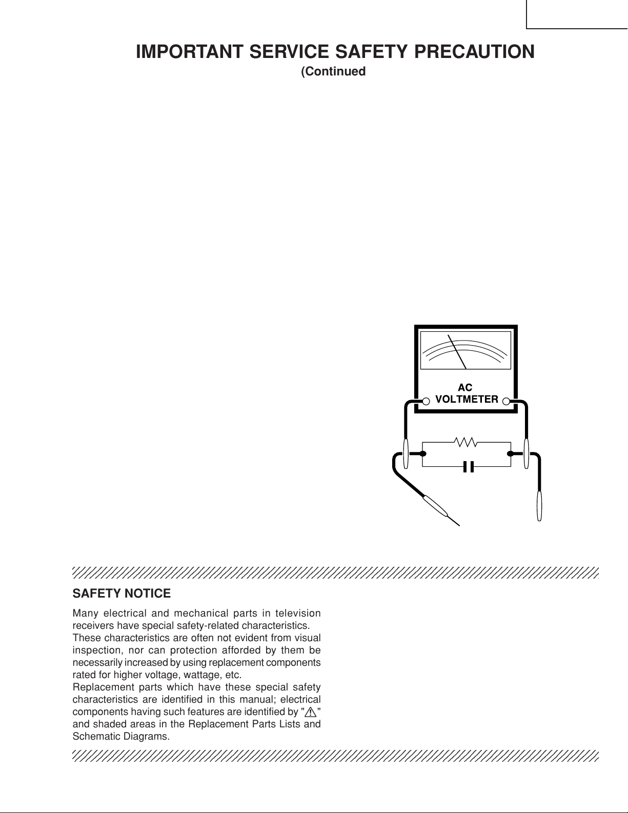
SAFETY NOTICE
Many electrical and mechanical parts in television
receivers have special safety-related characteristics.
These characteristics are often not evident from visual
inspection, nor can protection afforded by them be
necessarily increased by using replacement components
rated for higher voltage, wattage, etc.
Replacement parts which have these special safety
characteristics are identified in this manual; electrical
components having such features are identified by "å"
and shaded areas in the Replacement Parts Lists and
Schematic Diagrams.
234567890123456789012345678901212345678901234567890123456789012123456789012345678901234567890121
For continued protection, replacement parts must be
identical to those used in the original circuit. The use of
substitute replacement parts which do not have the same
safety characteristics as the factory recommended
replacement parts shown in this service manual, may
create shock, fire, X-radiation or other hazards.
3
Page 4
14LK11
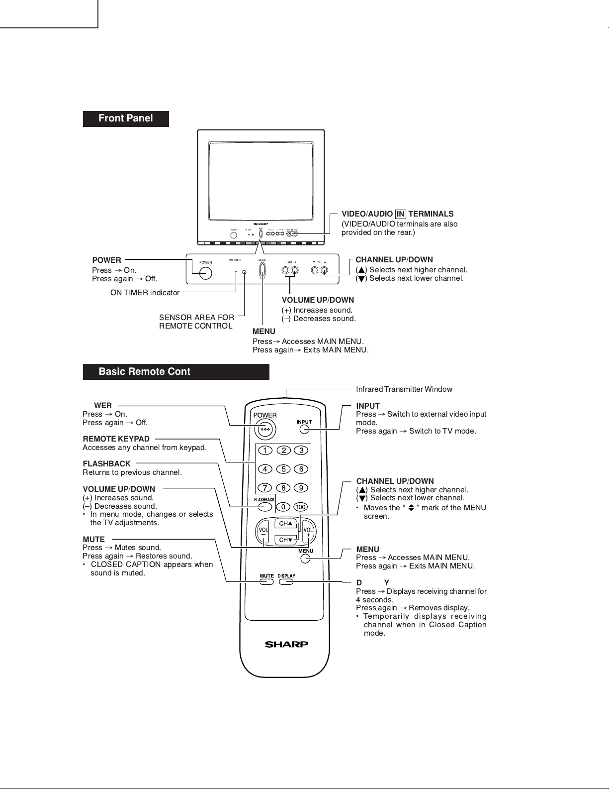
LOCATION OF USER'S CONTROL
Front Panel
POWER
Press®On.
Press again®Off.
ON TIMER indicator
SENSOR AREA FOR
REMOTE CONTROL
Basic Remote Control Functions
POWER
Press®On.
Press again®Off.
REMOTE KEYPAD
Accesses any channel from keypad.
FLASHBACK
Returns to previous channel.
VOLUME UP/DOWN
(+) Increases sound.
(Ð) Decreases sound.
¥ In menu mode, changes or selects
the TV adjustments.
MUTE
Press®Mutes sound.
Press again®Restores sound.
¥ CLOSED CAPTION appears when
sound is muted.
VIDEO/AUDIO TERMINALS
(VIDEO/AUDIO terminals are also
provided on the rear.)
CHANNEL UP/DOWN
( ) Selects next higher channel.
( ) Selects next lower channel.
VOLUME UP/DOWN
(+) Increases sound.
(Ð) Decreases sound.
MENU
Press®Accesses MAIN MENU.
Press again®Exits MAIN MENU.
Infrared Transmitter Window
INPUT
Press®Switch to external video input
mode.
Press again®Switch to TV mode.
CHANNEL UP/DOWN
( ) Selects next higher channel.
( ) Selects next lower channel.
¥ Moves the Ò Ó mark of the MENU
MENU
Press®Accesses MAIN MENU.
Press again®Exits MAIN MENU.
DISPLAY
Press®Displays receiving channel for
4 seconds.
Press again®Removes display.
¥ Temporarily displays receiving
IN
screen.
channel when in Closed Caption
mode.
TV
4
Page 5

14LK11
INSTALLATION AND SERVICE INSTRUCTIONS
Note: (1) When performing any adjustments to resistor controls and transformers use non-metallic
screwdrivers or TV alignment tools.
(2) Before performing adjustments, the TV set must be on at least 15 minutes.
CIRCUIT PROTECTION
The receiver is protected by a 3.15A fuse (F701),
mounted on PWB-A, wired into one side of the AC
line input.
+B DC REGULATOR CONFIRMATION
The + B DC output voltage adjustment is not included
in this circuit.However, should confirmation be
reguired proceed as follows.
1. Actuate receiver with 220V AC input voltage.
2. Receive a local channel.
3. Connect positive lead of digital voltmeter to C754
positive side on PWB-A ; negative lead to chassis
ground.
4. Confirm this voltage reading is as below.
CAUTION: The reading should be within 130 ± 2.0V DC
to ensure normal function and circuitry
reliability.
X-RADIATION PROTECTOR CIRCUIT TEST
After service has been performed on the horizontal
deflection system, high voltage system, B+ system,
test the X-Radiation protection circuit to ascertain
proper operation as follows:
HIGH VOLTAGE CHECK
High voltage is not adjustable but must be checked
to verify that the receiver is operating within safe
and efficient design limitations as specified checks
should be as follows:
1. Connect an accurate high voltage meter between
ground and anode of picture tube.
2. Operate receiver for at least 15 minutes at 110~220V
AC line voltage, with a strong air signal or a properly
tuned in test signal.
3. Receive a good local channel.
4. The voltage should be approximately, 23.5kV (at
picture MAX, Bright center condition).
If a correct reading cannot be obtained, check circuitry
for malfunctioning components. After the voltage test,
make Y-mute off to the normal mode.
1. Apply 220V AC using a variac transformer for accurate
input voltage.
2. Allow for warm up and adjust all customer controls
for normal picture and sound.
3. Receive a good local channel.
4. Connect a digital voltmeter to TP653 and make sure
that the voltmeter reads 21.1 ± 1.5 V.
5. Apply external 27.9V DC at TP653 by using an
external DC supply, TV must be shut off.
6. To reset the protector, unplug the AC cord and make
a short circuit between TP651 and TP652. Now make
sure that normal picture appears on the screen.
7. If the operation of the horizontal oscillator does not
stop in step 5, the circuit must be repaired before the
set is returned to the customer.
5
Page 6
14LK11
For adjustments of this model, the bus data is converted to various analog signals by the D/A converter
circuit.
Note: There are still a few analog adjustments in this series such as focus and master screen voltage.
Follow the steps below whenever the service adjustment is required. See "Table-B" to determine, if service adjustments are required.
1. Service mode
Before putting unit into the service mode, check that
customer adjustments are in the normal mode. Use
the reset function in the video adjustment menu to
ensure customer controls are in their proper (reset)
position.
2. Service item selection
Once in the service mode, press the Ch-up or Chdown button on the remote controller or at the set.
The service adjustment item will vary in increments
of one. Select the item you wish to adjust.
3. Data number selection
Press the Vol-up or down button to adjust the data
number.
To enter the service mode and exit service mode.
Short JA137&JA138 for 1 Second and release to switch
to the service mode position, and the microprocessor is
in input mode.(Adjustment through the I2C bus control.)
To exit the service mode, turn the television off by
pressing the power button.
DATA NUMBER
SERVICE ADJUSTMENT ITEM
25AGC:
Figure A.
6
Page 7
SUB
ADJ.
MODE
↓
MAX VOLUME (SUB-VOL)
↓
SUB CONTRAST (SUB-CON)
↓
SUB TINT (SUB-TINT)
↓
SUB COLOUR (SUB-COL)
↓
SUB BRIGHTNESS (SUB-BRI)
↓
SUB SHARPNESS (SUB-SHP)
↓
MAX HOTEL VOLUME (HTL-VOL)
↓
HOTEL PROGRAM NO(HTL-PRG)
↓
BLUE BACK CONTRAST (BB-CON)
↓
OSD GRB REFERENCE (RGB)
↓
BLACK LEVEL OFFSET R(CUT-R)
↓
BLACK LEVEL OFFSET G(CUT-G)
↓
CATHODE DRIVE LEVEL(CDL)
SERVICE MODE
(1) In the Service Mode, Key is used to select the mode in the following oreder.
AGC & WHITE POINT SUB
GEOMETRIC ADJ. ADJ.
MODE MODE MODE
FEATURE IC MTS
OPTION OPTION ADJ.
MODE MODE MODE
14LK11
OFFSET
ADJ.
MODE
AGC TAKE OVER POINT (AGC)
VERTICAL SLOPE (V-LIN)
VERTICAL AMP (V-AMP)
VERTICAL SHIFT (V-CENT)
VERTICAL ZOOM (V-ZOOM)
HORIZONTAL SHIFT (H-CENT)
EAST-WEST WIDTH (H-SIZE)
HORIZONTAL PARALLELOGRAM (EW//)
EAST-WEST PARABOLA / WIDTH (PARA)
EAST-WEST UPPER CORNER
PARABOLA (COR(U))
EAST-WEST LOWER CORNER
PARABOLA (COR(L))
EAST-WEST TRAPEZIUM (TRAPE)
HORIZONTAL BOW (HB)
S-CORRECTION (S-COR)
AGC &
GEOMETRIC
MODE
↓
↓
↓
↓
↓
↓
↓
↓
↓
↓
↓
↓
↓
↓
WHITE POINT
ADJ.
MODE
W.P. RED OFFSET HIGH /
OFFSET BLUE TONE (DRI-R-HI)
W.P. GREEN OFFSET HIGH /
OFFSET BLUE TONE (DRI-G-HI)
W.P.BLUE OFFSET HIGH /
OFFSET BLUE TONE (DRI-B-HI)
W.P. RED MH / STD (DRI-R-MH)
W.P. GREEN MH / STD (DRI-G-MH)
W.P. BLUE MH / STD (DRI-B-MH)
W.P. RED OFFSET ML /
OFFSET RED TONE (DRI-R-ML)
W.P. GREEN OFFSET ML /
OFFSET RED TONE (DRI-G-ML)
W.P. BLUE OFFSET ML /
OFFSET RED TONE (DRI-B-ML)
W.P. RED OFFSET LOW (DRI-R-LO)
W.P. GREEN OFFSET LOW (DRI-G-LO)
W.P. BLUE OFFSET LOW (DRI-B-LO)
↓
↓
↓
↓
↓
↓
↓
↓
↓
↓
↓
↓
7
Page 8

14LK11
OFFSET
ADJ.
MODE
Y-D TIME (TV) [ YD ] (DL-TV)
Y-D TIME (AV) [ YD ] (DL-AV)
INITIAL/DEFAULT LANGUAGE (INIT)
FAO-MAX VOLUME (FAO-VOL)
ENERGY SAVE OFFSET (ESV_OFFS)
CLOSE CAPTION POSITION (CCPOS)
↓
↓
↓
↓
↓
↓
IC
OPTION
MODE
VERTICAL SCAN DISABLE (VSD)
BLACK STRETCH (BKS)
AUTOMATIC VOLUME LEVELLING (AVL)
FAST FILTER IF-PLL ( FFI )
ENABLE VERTICAL GUARD ( EVG )
EHT TRACKING MODE ( EHT )
OVERSCAN SWITCH OFF (OSO)
AUTO COLOUR LIMIT (ACL)
FORCED COLOUR-ON (FCO)
VIDEO MUTE AT IDENT LOSS (VMI)
VIDEO MUTE AT PROGRAM/SOURCE CHANGE (VMC)
HOTEL MODE (HTL)
GAIN FM DEMODULATOR (BTSC)
CHARGE PUMP (CP)
FM WINDOW SELECTION (FMWS)
SOUND MUTE BIT 0 (SM0)
SOUND MUTE BIT 1 (SM1)
IF AGC SPEED BIT 0 (AGC0)
IF AGC SPEED BIT 1 (AGC1)
PHI 1 TIME CONSTANT FOR FE (FOA-FE)
PHI 1 TIME CONSTANT FOR FE (FOB-FE)
PHI 1 TIME CONSTANT FOR AV (FOA-AV)
PHI 1 TIME CONSTANT FOR AV (FOB-AV)
FORCED SLICING LEVEL FOR VERTICAL SYNC.(FSL)
SYNCHRONISATION OF OSD/TEXT DISPLAY (HP2)
RGB BLANK (RGBL)
↓
↓
↓
↓
↓
↓
↓
↓
↓
↓
↓
↓
↓
↓
↓
↓
↓
↓
↓
↓
↓
↓
↓
↓
↓
↓
MTS
ADJ.
MODE
ATTENUATE INPUT SIGNAL LEVEL (ATT)
VCO FREE RUNNING FREQUENCY ADJ. (VCO)
STEREO, SAP, DBX FILTER ADJ. (FILTER)
STEREO SEPARATION ADJUSTMENT (300HZ) (WIDEBAND)
STEREO SEPARATION ADJUSTMENT (3kHZ) (SPECTRAL)
BASS LEVEL (BASS)
TREBLE LEVEL (TREBLE)
↓
↓
↓
↓
↓
↓
↓
FEATURE
OPTION
MODE
↓
V-CHIP (V-CHIP)
MTS DECODING ENABLED (MTS)
DEMO MODE (DEMO)
REAL TIME CLOCK / ON TIMER (CLOCK)
ENERGY SAVE (E-SAVE)
PERSONAL PREFERENCE PROGRAM (P_PREF)
UNIVERSAL PLUS (UNIV+)
SPEAKER ON/OFF (SPEAKER)
FIXED AUDIO OUT (FAO)
VIEW TIMER (VIEW-TM)
FRENCH LANGUAGE (FRENCH)
EZ SETUP / AUTOPRESET (EZ-SETUP)
WHITE TEMP OR FAVORITE COLOR (W-TEMP)
AV ENABLED OR DISABLED (AV)
AV2 ENABLED OR DISABLED (AV2)
DYNAMIC SKIN CONTROL (DSK)
RATIO PRE- AND OVERSHOOT BIT 0 (RPO0)
RATIO PRE- AND OVERSHOOT BIT 1 (RPO1)
GAIN FM DEMODULATOR (AGN)
AUTO SWITCH OFF ENABLED (AUTO-OFF)
↓
↓
↓
↓
↓
↓
↓
↓
↓
↓
↓
↓
↓
↓
↓
↓
↓
↓
↓
FORWARD : CH DOWN KEY
REVERSE : CH UP KEY
( ) means OSD display.
Figure B: ADJUSTMENT CATEGORIES
1Press the CH DOWN/UP key on the remote controller to get ready to select the mode one by one.
2Press the CH DOWN/UP key on the remote controller to select the modes reversibly one by one.
3Using the VOLUME UP/DOWN key on the remote controller, the data can be modified.
(OSD disturbance can be erased by R/C display key)
8
Page 9
SERVICE MODE
14LK11
SERVICE
POSITION
AGC AGC TAKE OVER POINT 0~63 14 ADJ
V-LIN VERTICAL SLOPE 0~63 32 ADJ
V-AMP VERTICAL AMP 0~63 32 ADJ
V-CENT VERTICAL SHIFT 0~63 32 ADJ
V-ZOOM VERTICAL ZOOM 0~63 32 FIX
H-CENT HORIZONTAL SHIFT 0~63 32 ADJ
H-SIZE EAST-WEST WIDTH 0~63 32 FIX
EW// HORIZONTAL PARALLELOGRAM 0~63 32 FIX
PARA EAST-WEST PARABOLA / WIDTH 0~63 32 FIX
COR(U) EAST-WEST UPPER CORNER PARABOLA 0~63 32 FIX
COR(L) EAST-WEST LOWER CORNER PARABOLA 0~63 32 FIX
TRAPE EAST-WEST TRAPEZIUM 0~63 32 FIX
HB HORIZONTAL BOW 0~63 32 FIX
S-COR S-CORRECTION 0~63 0 FIX must be "17"
DRI-R-HI “W,P RED OFFSET HIGH / OFFSET BLUE TONE” 0~63 32 FIX must be "32"
DRI-G-HI W.P. GREEN OFFSET HIGH / OFFSET BLUE TONE 0~63 32 FIX must be "33"
DRI-B-HI W.P.BLUE OFFSET HIGH / OFFSET BLUE TONE 0~63 32 FIX must be "37"
DRI-R-MH W.P. RED MH / STD 0~63 25 FIX must be "32"
DRI-G-MH W.P. GREEN MH / STD 0~63 32 ADJ
DRI-B-MH W.P. BLUE MH / STD 0~63 32 ADJ
DRI-R-ML W.P. RED OFFSET ML / OFFSET RED TONE 0~63 32 FIX must be "32"
DRI-G-ML W.P. GREEN OFFSET ML / OFFSET RED TONE 0~63 32 FIX must be "32"
DRI-B-ML W.P. BLUE OFFSET ML / OFFSET RED TONE 0~63 32 FIX must be "25"
DRI-R-LO W.P. RED OFFSET LOW 0~63 32 FIX must be "32"
DRI-G-LO W.P. GREEN OFFSET LOW 0~63 32 FIX must be "22"
DRI-B-LO W.P. BLUE OFFSET LOW 0~63 32 FIX must be "19"
SUB-VOL MAX VOLUME 0~63 63 FIX must be "63"
SUB-CON SUB CONTRAST 0~63 63 FIX must be "52"
SUB-COL SUB COLOUR 0~63 32 ADJ
SUB-BRI SUB BRIGHTNESS 0~63 32 ADJ
SUB-TINT SUB TINT 0~63 32 ADJ
SUB-SHP SUB SHARPNESS 0~63 32 FIX must be "24"
HTL-VOL MAX HOTEL VOLUME 0~63 32 FIX
HTL-PRG HOTEL PROGRAM NO 0~125 or >125 for none 255 FIX
BB-CON BLUE BACK CONTRAST 0~15 10 FIX must be "5"
RGB OSD GRB REFERENCE 0~15 15 FIX must be "15"
CUT-R BLACK LEVEL OFFSET R 0~63 32 ADJ
CUT-G BLACK LEVEL OFFSET G 0~63 32 ADJ
CDL CATHODE DRIVE LEVEL 0~15 0 FIX must be "2"
DL-TV Y-D TIME (TV) [ YD ] 0~15 12 FIX must be "2"
DL-AV Y-D TIME (AV) [ YD ] 0~15 12 FIX must be "8"
INIT INITIAL/DEFAULT LANGUAGE 0(English), 1(Spanish), 0 FIX*
FAO-VOL FAO-MAX VOLUME 0~63 63 FIX must be "63"
ESV_OFFS ENERGY SAVE OFFSET 0~63 10 FIX must be "20"
CCPOS CLOSE CAPTION POSITION 0~255 32 ADJ
ATT ATTENUATE INPUT SIGNAL LEVEL 0~15 10 FIX
VCO VCO FREE RUNNING FREQUENCY ADJ. 0~63 32 FIX
FILTER “STEREO, SAP, DBX FILTER ADJ. “ 0~63 28 FIX
WIDEBAND STEREO SEPARATION ADJUSTMENT (300HZ) 0~63 32 FIX
SPECTRAL STEREO SEPARATION ADJUSTMENT (3kHZ) 0~63 27 FIX
BASS BASS LEVEL 0~15 8 FIX
TREBLE TREBLE LEVEL 0~15 8 FIX
VSD VERTICAL SCAN DISABLE 0 or 1 when item selected 0 FIX
BKS BLACK STRETCH 0(disable) or1(enable) 1 FIX
AVL AUTOMATIC VOLUME LEVELLING 0(disable) or1(enable) 1 FIX
FFI FAST FILTER IF-PLL 0(disable) or1(enable) 0 FIX
EVG ENABLE VERTICAL GUARD 0(disable) or1(enable) 1 FIX
EHT EHT TRACKING MODE 0(disable) or1(enable) 1 FIX
OSO OVERSCAN SWITCH OFF 0(disable) or1(enable) 0 FIX
ACL AUTO COLOUR LIMIT 0(disable) or1(enable) 0 FIX
FCO FORCED COLOUR-ON 0(disable) or1(enable) 0 FIX
VMI VIDEO MUTE AT IDENT LOSS 0(disable) or1(enable) 1 FIX
VMC VIDEO MUTE AT PROGRAM/SOURCE CHANGE 0(disable) or1(enable) 1 FIX
HTL HOTEL MODE 0(disable) or1(enable) 0 FIX
BTSC GAIN FM DEMODULATOR 0(disable) or1(enable) 0 FIX
CP CHARGE PUMP 0(fast tuning) or 1 0 FIX
ADJUST ITEM
RANGE
2(French)
(moderate speed tuning)
DATA
INITIAL VALUE
FIX/ADJ
REMARK
9
Page 10

14LK11
SERVICE
POSITION
FMWS FM WINDOW SELECTION 0(disable) or1(enable) 0 FIX
SM0 SOUND MUTE BIT 0 (SM0) 0(disable) or1(enable) 1 FIX
SM1 SOUND MUTE BIT 1 0(disable) or1(enable) 0 FIX
AGC0 IF AGC SPEED BIT 0 0(disable) or1(enable) 1 FIX
AGC1 IF AGC SPEED BIT 1 0(disable) or1(enable) 0 FIX
FOA-FE PHI 1 TIME CONSTANT FOR FE 0(disable) or1(enable) 0 FIX
FOB-FE PHI 1 TIME CONSTANT FOR FE 0(disable) or1(enable) 0 FIX
FOA-AV PHI 1 TIME CONSTANT FOR AV 0(disable) or1(enable) 1 FIX
FOB-AV PHI 1 TIME CONSTANT FOR AV 0(disable) or1(enable) 1 FIX
FSL FORCED SLICING LEVEL FOR VERTICAL SYNC. 0(disable) or1(enable) 0 FIX
HP2 SYNCHRONISATION OF OSD/TEXT DISPLAY 0(disable) or1(enable) 0 FIX
RGBL RGB BLANK 0(disable) or1(enable) 0 FIX
V-CHIP V-CHIP 0(disable) or1(enable) 0 FIX
MTS MTS DECODING ENABLED 0(disable) or1(enable) 0 FIX
DEMO DEMO MODE 0(disable) or1(enable) 1 FIX
CLOCK REAL TIME CLOCK / ON TIMER 0(disable) or1(enable) 1 FIX*
E-SAVE ENERGY SAVE 0(disable) or1(enable) 1 FIX
P_PREF PERSONAL PREFERENCE PROGRAM 0(disable) or1(enable) 0 FIX
UNIV+ UNIVERSAL PLUS 0(disable) or1(enable) 0 FIX
SPEAKER SPEAKER ON/OFF 0(disable) or1(enable) 0 FIX
FAO FIXED AUDIO OUT 0(disable) or1(enable) 0 FIX
VIEW-TM VIEW TIMER 0(disable) or1(enable) 1 FIX*
FRENCH FRENCH LANGUAGE 0(disable) or1(enable) 1 FIX
EZ-SETUP EZ SETUP / AUTOPRESET 0(AUTOPRESET) or 1 FIX
W-TEMP WHITE TEMP OR FAVORITE COLOR 0(FC) or 1(WT) 0 FIX
AV AV ENABLED OR DISABLED 0(without ext. source) or 0 FIX
AV2 AV2 ENABLED OR DISABLED 0(1 input) or 1(2 input) 0 FIX
DSK DYNAMIC SKIN CONTROL 0(disable) or1(enable) 0 FIX
RPO0 RATIO PRE- AND OVERSHOOT BIT 0 0(disable) or1(enable) 0 FIX
RPO1 RATIO PRE- AND OVERSHOOT BIT 1 0(disable) or1(enable) 0 FIX
AGN GAIN FM DEMODULATOR 0(normal) or1(+6dB) 0 FIX
AUTO-OFF AUTO SWITCH OFF ENABLED 0(disable) or1(enable) 1 FIX
ADJUST ITEM
RANGE
1(EZ SETUP)
1(with external source)
DATA
INITIAL VALUE
FIX/ADJ
REMARK
Table - A
Holding down to short JA137 & JA138 and turn on the main power SW will automatically write the initial values into
IC1003.
This is only can done when a new EEPROM is used. (Judge with the first 4 bytes.)
PART REPLACED
IC801
IC1003
CRT
NECESSARY
ADJUSTMENT
X
X
UNNECESSARY
X
NOTES
Data is stored in IC1003.
Holding down to short JA137 & JA138 and turn on the main
power SW will automatically write the initial values into IC1003.
This is only can done when a new EEPROM is used. (Judge
with the first 4 bytes.)
Adjust items related to picture tube only.
Table - B
10
Page 11

Ë
WAVEFORM 1
YCYGMGR BW
SAME LEVEL
SERVICE ADJUSTMENT
RF AGC Adjustment
1. Receive a good local channel.
2. Enter the service mode signal category and select
the service adjustment "AGC".
3. Set the data value to point where no noise or beat
appears.
4. Select another channel to confirm that no noise or
beat appears.
CHROMA ADJUSTMENT
No. Adjusting point Adjusting procedure/conditions Waveform and others
1
SUB-TINT (I
BUS CONTROL)
2
C
1. Receive the "Colour Bar" signal through AV in.
2. Connect the oscilloscope to TP853 (Pin (5) of
P882) BLUE-OUT.
» Range : 100mV/div. (AC)(Use Probe 10:1)
» Sweep time : 10 µsec/div.
3. Call the "SUB-TINT" mode in service mode. Adjust the "SUB-TINT" bus data to obtain the waveform shown as Fig 1.
4. "SUB-TINT" bus data decrease 4 steps to get final
waveform. (Fig 2.)
5. Clear the SERVICE mode.
Fig 1
FINAL WAVEFORM
Fig 2
14LK11
HORIZONTAL AND VERTICAL DEFLECTION LOOP ADJUSTMENT
No. Adjusting point Adjusting procedure/conditions Waveform and others
V-SLOPE(I2C
1
BUS CONTROL)
V-CENTER (I2C
2
BUS CONTROL)
3
V - AMP (I2C
BUS CONTROL)
4
S-CORRECTION (I2C
BUS CONTROL)
H - CENTER
5
Focus
6
adjustment
1. Receive Monoscope Pattern Signal.
2. Call the "V-LIN" mode.
3. Increase or decrease "V-LIN" by Volume key till
the horizontal line in the center of monoscope is
just at the position where the blanking starts.
1. Call the "V-CENT" mode.
2. Increase or decrease "V-CENT" by Volume key till
the picture is centered.
1. Call the "V-AMP" mode.
2. Increase or decrease "V - AMP" by Volume key to
set overscan of 10.0% typical.
Adjustment Spec 10.0% range ±1%.
FIXED DATA, NO NEED TO ADJUST.
1. Call the "H-CENT" mode.
2. Increase or decrease "H-CENT" by Volume key
to center the picture horizontal.
1. Receive the "Monoscope Pattern" signal.
2. Press R/C to set Picture NORMAL condition.
3. Adjust the focus control to get the best focus.
11
Page 12

14LK11
1 2 3 4 5
CRT CUT-OFF, BACKGROUND AND SUB-CONTRAST ADJUSTMENT
No. Adjusting point Adjusting procedure/conditions Waveform and others
CRT CUTOFF
1
ADJUSTMENT
(I2C BUS
CONTROL)
SUB-BRIGHT-
2
NESS
ADJUSMENT
(I2C BUS
CONTROL)
WHITE BAL-
3 # 11,600° K X : 0.273
ANCE SERVICE MODE
ADJ. (I2C BUS
CONTROL)
1. Switch TV to VIDEO mode,BLUE BACK OFF, with
NO VIDEO signal.
2. Press R/C to set Picture Normal condition.
3. Connect the oscilloscope to Red OUT from
IC801.(TP47R)
Range : 1 V/Div (DC)
Sweep : 5 msec/Div
4. Adjust SCREEN VR ,so that the tip of signal reach
3.0 Vdc + 0.1 Vdc.
1. Call " SUB-BRI" in service mode. (Receive Crosshatch pattern with 5 black level windows)
2. Adjust the " SUB BRIGHT " bus data in order that
the line 1, 2 and 3 have the same darkness
wherelse line 4 is slightly brighter than line 1, 2
and 3 and finally line 5 will be the brighter than
line 4.
1. Receive the "Monoscope Pattern" signal.
2. Press R/C to set Picture NORMAL condition.
3. Connect the DC miliammeter between the TP 602
( - ) TP 603 ( + ).
4. Check Beam current should be around (720µA)
5. Set it to service mode and adjust the DRI-G-MH,
& DRI-B-MH data to have a colour temperature
of 11,600°K ( white ).
6. Receive "WHITE" pattern, WITH BURST signal,
and set BRIGHTNESS Y by generator, to ** 10
cd/m2 (MINOLTA CA-100) by reducing LUMINATE
Y signal.
7. Adjust "CUT-R" & "CUT-G" to get 11,600°K. Then
go back NORMAL mode (HIGH BRIGHT**) to
check colour temperature. If out of range, back
to (1).
3.0Vdc
1 V
0
1, 2, 3 are in same black level.
Y : 0.280
( MINOLTA COLOUR ANALYZER
CA-100)
*NOTE: Above DATA can be UP/
DOWN by volume key.
LOW HIGH
14" 1.8cd/m2115cd/m
* 11,600° K
DRI-GW="DRI-GS"DATA-5
DRI-BW="DRI-BS" DATA-5
2
Maximum
4
beam check
Note: This adjustment must be done after
warming up the unit for 30 minutes or
longer with a beam current over 500µA.
DRI-R-MH=32 (FIXED)
DRI-G-MH=33 (FIXED)
DRI-B-MH=37 (FIXED)
DRI-R-MH=32 (FIXED)
1. Receive the "Monoscope Pattern" signal.
2. Press R/C to set Picture NORMAL condition.
3. Connect the DC miliammeter between TP603 (+)
and TP602 (–).
(Full Scale: 3 mA Range)
4. Beam current must be within 720 ± 50 µA.
12
Page 13

CHASSIS LAYOUT
H
G
F
14LK11
E
D
C
B
A
654321
13
Page 14

14LK11
BLOCK DIAGRAM
H
G
F
E
D
C
B
A
654321
14
Page 15

DESCRIPTION OF SCHEMATIC DIAGRAM
14LK11
NOTES:
1. The unit of resistance "ohm" is omitted.
(K=kΩ=1000Ω, M=MΩ)
2. All resistors are 1/16 watt, unless otherwise noted.
3. All capacitors are µF, unless otherwise noted.
(P=pF=µµF)
4. (G) indicates ±2% tolerance may be used.
5. indicates line isolated ground.
6. indicates hot ground.
VOLTAGE MEASUREMENT CONDITIONS:
1. All DC voltages are measured with DVM connected
between points indicated and chassis ground, line
voltage set at 120V AC and all controls set for normal
picture unless otherwise indicated.
2. All voltages measured with 1000µV B & W or Color
signal.
WAVEFORMS
WAVEFORM MEASUREMENT CONDITIONS:
1. Photographs taken on a standard gated color bar
signal, the tint setting adjusted for proper color. The
wave shapes at the red, green and blue cathodes of
the picture tube depend on the tint, color level and
picture control.
2.
indicates waveform check points (See chart,
waveforms are measured from point indicated to
chassis ground.)
å
AND SHADED ( ) COMPONENTS
= SAFETY RELATED PARTS.
'
MARK= X-RAY RELATED PARTS.
This circuit diagram is a standard one, printed circuits
may be subject to change for product improvement
without prior notice.
11.00Vp-p
Horiz Rate Horiz Rate Horiz Rate Horiz Rate Horiz Rate
667Vp-p
Horiz Rate Vert Rate Horiz RateHoriz Rate Horiz Rate
q8.40Vp-p
22.8Vp-p
780Vp-p
w48.8Vp-p
32.6Vp-p
83.00Vp-p 92.3Vp-p
e98Vp-p
42.7Vp-p
r1200Vp-p
565Vp-p
0116Vp-p
t415Vp-p
Horiz Rate Horiz Rate Horiz Rate Power Supply RateVert Rate
15
Page 16

14LK11
16
Page 17

14LK11
17
Page 18

14LK11
VB34EAK02X+1E
18
Page 19

PRINTED WIRING BOARD ASSEMBLIES
H
G
F
14LK11
PWB-B: CRT Unit (Wiring Side)
E
D
C
PWB-B: CRT Unit (Chip Parts Side)
B
A
654321
19
Page 20

14LK11
H
G
F
E
D
C
B
A
PWB-A: MAIN Unit (Wiring Side)
654321
20
Page 21

14LK11
H
G
F
E
D
C
B
A
PWB-A: MAIN Unit (Chip Parts Side)
654321
21
Page 22

14LK11
Ref. No. Part No. ★ Description Code Ref. No. Part No. ★ Description Code
PARTS LIST
PARTS REPLACEMENT
Replacement parts which have these special safety characteristics
identified in this manual; electrical components having such features
are identified by å and shaded areas in the Replacement Parts Lists
and Schematic Diagrams. The use of a substitute replacement part
which dose no have the same safety characteristic as the factory
recommended replacement parts shown in this service manual may
create shock, fire or other hazards.
NOTE : THE PARTS HERE SHOWN ARE SUPPLIED AS AN
PWB-A: DUNTKA541WEE1
MAIN UNIT
TUNER
ASSEMBLY BUT NOT INDEPENDENTLY.
å TU201 VTUENV56D82-1 J Tuner AT
"HOW TO ORDER REPLACEMENT PARTS"
To have your order filled promptly and correctly, please furnish the
following informations.
1. MODEL NUMBER 2. REF. NO.
3. PART NO. 4. DESCRIPTION
★ MARK : SPARE PARTS-DELIVERY SECTION
' MARK : X- RAY RELATED PARTS
Ref. No. Part No. ★ Description Code
PICTURE TUBE
å V101 VB34EAK02X+1E R Picture Tube BM
å L703 RCiLG0068PEZZ R Degaussing Coil AH
å DY601 RCiLH0225PEZZ R Deflection Yoke BA
PMAGF3041CEZZ J Degaussing Coil AG
-Purity and Static
Convergence
PSPAG0004PEZZ R Wedge(Gum), Yoke AB
QEARC1436PEZZ R Grounding Strap AE
MSPRT0001PEFJ R Spring for CRT AC
PRINTED WIRING BOARD ASSEMBLIES
(NOT REPLACEMENT ITEM)
PWB-A DUNTKA541WEE1 – MAIN Unit —
PWB-B DUNTKA542WEA0 – CRT Unit —
INTEGRATED CIRCUITS
IC302 VHiAN7511//-1 J An7511 AC
å IC501 VHIAN5522++-1 X An5522 AD
IC601 VHiKA7808AP-1 J Kia7808api AC
IC701 VHiSTRG5653-1 X Strg5653 AH
IC801 RH-iX3564CEZZ X I.C. AT
IC1003 VHiBR24C02F1E* J I.C. AC
TRANSISTORS
You can substitute "VS2SC2462-C-1" for "VS2SD601AR/-1".
Q201 VS2SC2735//1E J C2735
Q253 VS2SD601A//-1 J D601A AA
Q254 VS2SD601A//-1 J D601A AA
Q601 VS2SC3207//-1 J C3207 AB
Q602 VS2SD2586//1E J D2586 AF
Q603 VS2SC3198-G-1 J C3198-G AB
Q751 VS2SC3198-G-1 J C3198-G AB
Q752 VS2SC3198-G-1 J C3198-G AB
Q801 VS2SB709A//-1 J B709A AB
Q802 VS2SB709A//-1 J B709A AB
DIODES
D201 RH-EX0676GEZZ J Zener Diode, 33V AB
D302 VHD1SS119//-1 J Diode AA
å D331 RH-DX0302CEZZ J Diode AB
D502 RH-EX0615GEZZ J Zener Diode, 5V AB
D503 VHD1SS119//-1 J Diode AA
D505 RH-DX0441CEZZ J Diode AB
D508 RH-DX0131CEZZ J Diode AB
D509 RH-EX0665GEZZ J Zener Diode, 24V AB
D511 VHD1SS119//-1 J Diode AA
D531 RH-EX0627GEZZ J Zener Diode, 8.2V AB
D532 RH-EX0627GEZZ J Zener Diode, 8.2V AB
D601 RH-DX0475CEZZ J Diode AA
å D602 VHD1SS244//-1 J Diode AB
å D603 RH-EX0667GEZZ J Zener Diode, 27V AB
å D606 RH-DX0131CEZZ J Diode AB
å D608 RH-DX0468CEZZ J Diode AB
D651 RH-EX0627GEZZ J Zener Diode, 8.2V AB
D653 VHD1SS119//-1 J Diode AA
D701 RH-DX0476CEZZ J Diode AC
D705 VHD1SS82///1A J Diode AB
D706 VHD1SS82///1A J Diode AB
D707 VHD1SS82///1A J Diode AB
å D751 RH-DXA006WJZZ J Diode AB
å D752 RH-DX0131CEZZ J Diode AB
D754 RH-EX0616GEZZ J Zener Diode, 5.6V AB
D755 RH-EX0603GEZZ J Zener Diode, 3.9V AB
D801 VHD1SS119//-1 J Diode AA
D802 VHD1SS119//-1 J Diode AA
D803 VHD1SS119//-1 J Diode AA
D804 VHD1SS119//-1 J Diode AA
D805 VHD1SS119//-1 J Diode AA
D806 VHD1SS119//-1 J Diode AA
D1001 RH-PX0013PEZZ R Photodiode AB
D1004 VHD1SS119//-1 J Diode AA
D1012 RH-EX0611GEZZ J Zener Diode, 5.1V AB
D1018 RH-EX0263TAZZ J Zener Diode, 8.3V AB
D1019 RH-EX0263TAZZ J Zener Diode, 8.3V AB
D1020 RH-EX0263TAZZ J Zener Diode, 8.3V AB
D1021 RH-EX0263TAZZ J Zener Diode, 8.3V AB
22
Page 23

14LK11
Ref. No. Part No. ★ Description Code Ref. No. Part No. ★ Description Code
PWB-A: DUNTKA541WEE1
MAIN UNIT (Continued)
D1022 RH-EX0263TAZZ J Zener Diode, 8.3V AB
D1023 RH-EX0263TAZZ J Zener Diode, 8.3V AB
å VA701 RH-VX0073CEZZ X Varistor AB
PACKAGED CIRCUITS
PR702 RMPTP0028CEZZ J Packaged Circuit AC
X1001 RCRSB0300CEZZ J Crystal AC
FILTERS
CF253 RFILC0013CEZZ J Filter AB
SF201 RFILCA015WJZZ J S.A.W. Filter AC
COILS
L202 VP-DF270K0000 J Peaking 27 µHAB
L203 VP-DF270K0000 J Peaking 27 µHAB
L204 VP-XF1R2K0000 J Peaking 1.2 µHAB
L253 VP-XF120K0000 J Peaking 12µHAB
å L701 RCiLF0096PEZZ R Coil AC
å L751 RCiLP0225CEZZ J Coil AF
L802 VP-DF100K0000 J Peaking 10µHAB
L803 VP-DF100K0000 J Peaking 10 µHAB
L1030 VP-DF100K0000 J Peaking 10µHAB
L1050 VP-DF100K0000 J Peaking 10µHAB
L1051 VP-DF100K0000 J Peaking 10µHAB
TRANSFORMERS
å T601 RTRNZ0144PEZZ R Transformer AB
å T602 RTRNF0228PEZZ X H-Volt Transformer AQ
å T701 RTRNW0015PEN1 X Transformer AE
CAPACITORS
[EL.··· Electrolytic, M-Poly.··· Metalized Polypro Film]
C201 VCEA0A1CW476M J 47 16V EL. AB
C202 VCEA0A1AW337M+X 330 10V EL. AB
C205 VCKYCY1HF103Z J 0.01 50V Ceramic AA
C206 VCEA0A1HW105M J 1.0 50V EL. AB
C207 VCKYCY1HB103K J 0.01 50V Ceramic AA
C208 VCKYCY1HB103K J 0.01 50V Ceramic AA
C209 VCKYCY1HB103K J 0.01 50V Ceramic AA
C210 VCKYCY1HF103Z J 0.01 50V Ceramic AA
C211 VCKYCY1HF103Z J 0.01 50V Ceramic AA
C231 VCKYCY1HF223Z J 0.022 50V Ceramic AA
C232 VCKYCY1HB821K J 820p 50V Ceramic AA
C233 VCKYCY1HB472K J 4700p 50V Ceramic AA
C234 VCKYCY1EF104Z J 0.1 25V Ceramic AA
C251 VCKYCY1HF223Z J 0.022 50V Ceramic AA
C252 VCEA0A1CW107M J 100 16V EL. AB
C301 VCEA0A1CW477M J 470 16V EL. AB
C304 VCEA0A1HW106M J 10 50V EL. AB
C310 VCEA0A1HW225M J 2.2 50V EL. AB
C312 VCEA0A1HW225M J 2.2 50V EL. AB
C313 VCKYCY1HB332K J 3300p 50V Ceramic AA
å C332 VCQYTA1HM103J J 0.01 50V Mylar AB
å C333 VCEA0A1CW108M J 1000 16V EL. AB
C356 VCKYCY1HB472K J 4700p 50V Ceramic AA
C359 VCEA0A1CW106M J 10 16V EL. AB
C360 VCEA0A1HW225M J 2.2 50V EL. AB
C409 VCKYCY1EF104Z J 0.1 25V Ceramic AA
C410 VCKYCY1EF104Z J 0.1 25V Ceramic AA
C411 VCKYCY1HB102K J 1000p 50V Ceramic AA
C501 VCKYPA1HB102K J 1000p 50V Ceramic AA
C504 VCKYCY1HB103K J 0.01 50V Ceramic AA
C505 VCEA0A1HW107M J 100 50V EL. AB
C507 VCKYCY1HB103K J 0.01 50V Ceramic AA
C508 VCFYSA1JB224J+ X 0.22 63V Ceramic AB
C509 VCEA0A1CW477M J 470 16V EL. AB
C510 VCKYPA2HB102K J 1000p 500V Ceramic AB
C514 VCFYSA1JB563J+ X 0.056 63V Ceramic AB
C531 VCKYCY1HB102K J 1000p 50V Ceramic AA
C532 VCKYCY1HB102K J 1000p 50V Ceramic AA
C533 VCQYTA1HM104J J 0.1 50V Mylar AB
C601 VCQYTA1HM563J J 0.056 50V Mylar AB
C602 VCEA0A1HW475M J 4.7 50V EL. AB
C603 VCEA0A1HW105M J 1.0 50V EL. AB
C604 VCEA0A2EW106M J 10 250V EL. AD
C605 VCKYPA2HB102K J 1000p 500V Ceramic AB
C606 VCFPVC2DB334J J 0.33 200V M-Poly. AB
C607 VCFPVC3ZA532H X 5300p 1.5kV M-Poly. AB
C608 VCKYPA2HB102K J 1000p 500V Ceramic AB
C610 VCEA0A1CW108M J 1000 16V EL. AB
C611 VCEA0A1EW476M J 47 25V EL. AB
C612 VCEA0A1CW477M J 470 16V EL. AB
C620 VCKYPA2HB102K J 1000p 500V Ceramic AB
C640 VCFYSB2EB823J J 0.082 250V Ceramic AB
C651 VCQYTA1HM222J J 2200p 50V Mylar AB
C652 VCQYTA1HM472J J 4700p 50V Mylar AB
C653 VCEA0A1HW105M J 1.0 50V EL. AB
C654 VCKYCY1HF223Z J 0.022 50V Ceramic AA
C655 VCEA0A1HW106M J 10 50V EL. AB
C656 VCEA0A1HW224M J 0.22 50V EL. AB
C657 VCKYCY1EF104Z J 0.1 25V Ceramic AA
C658 VCKYCY1EF104Z J 0.1 25V Ceramic AA
C701 RC-FZ036SCEZZ J 0.1 275V Ceramic AB
or
RC-FZ035SGEZZ
or
RC-FZ038SCEZZ
C702 RC-KZ0029CEZZ J 0.01 250V Ceramic AB
C703 RC-KZ0029CEZZ J 0.01 250V Ceramic AB
C704 RC-KZ0029CEZZ J 0.01 250V Ceramic AB
C705 RC-EZ1044CEZZ J 150 400V EL. AF
C709 RC-KZ0039CEZZ J 680P 2kV Ceramic AB
C710 VCEA0A1HW476M J 47 50V EL. AB
C711 VCKYPA1HB102K J 1000p 50V Ceramic AA
C712 VCKYPA1HB471K J 470p 50V Ceramic AA
C751 RC-KZ0092GEZZ J
å C752 VCKYPH3DB561K J 560p 2kV Ceramic AB
å C753 RC-EZ0724CEZZ J 100 160V EL. AC
å C754 RC-EZ0638CEZZ J 33 160V EL. AC
å C755 VCEA0A1CW108M J 1000 16V EL. AB
å C756 VCQYTA1HM103J J 0.01 50V Mylar AB
C759 VCEA0A0JW477M J 470 6.3V EL. AB
C760 VCEA0A0JW228M J 2200 6.3V EL. AB
C801 VCEA0A1HW105M J 1.0 50V EL. AB
C802 VCEA0A1CW337M J 330 16V EL. AB
C803 VCEA0A1CW107M J 100 16V EL. AB
C804 VCKYCY1HB222K J 2200p 50V Ceramic AA
C805 VCKYD41HB102K J 1000p 50V Ceramic AA
C806 VCKYD41HB102K J 1000p 50V Ceramic AA
C807 VCKYD41HB102K J 1000p 50V Ceramic AA
C808 VCEA0A1CW107M J 100 16V EL. AB
C809 VCKYCY1CF474Z J 0.47 16V Ceramic AB
C810 VCKYCY1CF474Z J 0.47 16V Ceramic AB
C811 VCEA0A1CW107M J 100 16V EL. AB
C812 VCFYFA1HA224J J 0.22 50V Mylar AB
C813 VCFYFA1HA224J J 0.22 50V Mylar AB
C814 VCKYCY1HB471K J 470p 50V Ceramic AB
C816 VCKYCY1HB471K J 470p 50V Ceramic AB
C1001 VCEA0A0JW107M J 100 6.3V EL. AB
C1002 VCEA0A0JW107M J 100 6.3V EL. AB
C1003 VCEA0A1CW106M J 10 16V EL. AB
C1004 VCKYCY1CF474Z J 0.47 16V Ceramic AB
C1005 VCKYCY1CF474Z J 0.47 16V Ceramic AB
C1006 VCEA0A1CW106M J 10 16V EL. AB
C1008 VCCCCY1HH330J J 33p 50V Ceramic AA
C1009 VCCCCY1HH330J J 33p 50V Ceramic AA
C1010 VCEA0A0JW107M J 100 6.3V EL. AB
C1011 VCKYCY1CF474Z J 0.47 16V Ceramic AB
C1012 VCKYCY1CF474Z J 0.47 16V Ceramic AB
C1013 VCEA0A0JW107M J 100 6.3V EL. AB
C1016 VCQYTA1HM104J J 0.1 50V Mylar AB
C1018 VCKYCY1HB221K J 220p 50V Ceramic AA
C1024 VCQYTA1HM104J J 0.1 50V Mylar AB
C1026 VCEA0A0JW107M J 100 6.3V EL. AB
0.0033 AC250V
Ceramic AB
23
Page 24

14LK11
Ref. No. Part No. ★ Description Code Ref. No. Part No. ★ Description Code
PWB-A: DUNTKA541WEE1
MAIN UNIT (Continued)
RESISTORS
[M-Ox.··· Metal Oxide, Metal Film··· M-Film]
RJ2 VRS-CY1JF000J J 0 1/16W M-Ox. AA
RJ4 VRS-CY1JF000J J 0 1/16W M-Ox. AA
RJ8 VRS-CY1JF000J J 0 1/16W M-Ox. AA
RJ9 VRS-CY1JF000J J 0 1/16W M-Ox. AA
RJ10 VRS-CY1JF000J J 0 1/16W M-Ox. AA
RJ13 VRS-CY1JF000J J 0 1/16W M-Ox. AA
RJ14 VRS-CY1JF000J J 0 1/16W M-Ox. AA
RJ15 VRS-CY1JF000J J 0 1/16W M-Ox. AA
RJ16 VRS-CY1JF000J J 0 1/16W M-Ox. AA
RJ17 VRS-CY1JF000J J 0 1/16W M-Ox. AA
RJ19 VRS-CY1JF000J J 0 1/16W M-Ox. AA
RJ21 VRS-CY1JF000J J 0 1/16W M-Ox. AA
RJ26 VRS-CY1JF000J J 0 1/16W M-Ox. AA
RJ28 VRS-CY1JF000J J 0 1/16W M-Ox. AA
RJ31 VRS-CY1JF000J J 0 1/16W M-Ox. AA
RJ32 VRS-CY1JF000J J 0 1/16W M-Ox. AA
RJ35 VRS-CY1JF000J J 0 1/16W M-Ox. AA
RJ37 VRS-CY1JF000J J 0 1/16W M-Ox. AA
RJ38 VRS-CY1JF000J J 0 1/16W M-Ox. AA
RJ41 VRS-CY1JF000J J 0 1/16W M-Ox. AA
RJ42 VRS-CY1JF000J J 0 1/16W M-Ox. AA
RJ43 VRS-CY1JF000J J 0 1/16W M-Ox. AA
RJ46 VRS-CY1JF000J J 0 1/16W M-Ox. AA
RJ49 VRS-CY1JF000J J 0 1/16W M-Ox. AA
RJ50 VRS-CY1JF000J J 0 1/16W M-Ox. AA
RJ51 VRS-CY1JF000J J 0 1/16W M-Ox. AA
RJ52 VRS-CY1JF000J J 0 1/16W M-Ox. AA
RJ53 VRS-CY1JF000J J 0 1/16W M-Ox. AA
RJ70 VRS-CY1JF000J J 0 1/16W M-Ox. AA
RJ71 VRS-CY1JF000J J 0 1/16W M-Ox. AA
RJ72 VRS-CY1JF000J J 0 1/16W M-Ox. AA
RJ73 VRS-CY1JF000J J 0 1/16W M-Ox. AA
RJ75 VRS-CY1JF000J J 0 1/16W M-Ox. AA
R201 VRS-CY1JF101J J 100 1/16W M-Ox. AA
R202 VRS-CY1JF101J J 100 1/16W M-Ox. AA
R205 VRS-CY1JF680J J 68 1/16W M-Ox. AA
R206 VRS-CY1JF122J J 1.2k 1/16W M-Ox. AA
R207 VRS-CY1JF221J J 220 1/16W M-Ox. AA
R208 VRS-CY1JF122J J 1.2k 1/16W M-Ox. AA
R209 VRS-CY1JF392J J 3.9k 1/16W M-Ox. AA
R212 VRS-CY1JF332J J 3.3k 1/16W M-Ox. AA
R216 VRS-RG3LB223J+ X 22k 3W M-Ox. AB
R219 VRD-RA2BE392J J 3.9k 1/8W Carbon AA
R230 VRS-CY1JF473J* J 220 1/16W M-Ox. AA
R231 VRD-RA2BE681J J 680 1/8W Carbon AA
R232 VRS-CY1JF272J J 2.7k 1/16W M-Ox. AA
R233 VRS-CY1JF101J J 100 1/16W M-Ox. AA
R234 VRS-CY1JF391J J 390 1/16W M-Ox. AA
R257 VRS-CY1JF181J J 180 1/16W M-Ox. AA
R258 VRS-CY1JF151J J 150 1/16W M-Ox. AA
R259 VRS-CY1JF471J J 470 1/16W M-Ox. AA
R260 VRS-CY1JF392J J 3.9k 1/16W M-Ox. AA
R261 VRS-CY1JF223J J 22k 1/16W M-Ox. AA
R262 VRS-CY1JF560J J 56 1/16W M-Ox. AA
R263 VRS-CY1JF560J J 56 1/16W M-Ox. AA
R301 VRS-CY1JF101J J 100 1/16W M-Ox. AA
R304 VRS-CY1JF683J J 68k 1/16W M-Ox. AA
R310 VRS-CY1JF473J J 47k 1/16W M-Ox. AA
R311 VRS-CY1JF473J J 47k 1/16W M-Ox. AA
R313 VRS-CY1JF102J J 1.0k 1/16W M-Ox. AA
R314 VRS-CY1JF103J J 10k 1/16W M-Ox. AA
R315 VRS-CY1JF392J J 3.9k 1/16W M-Ox. AA
R320 VRN-RL3DB4R7J+ X 4.7 2W M-Film AB
R333 VRS-CY1JF101J J 100 1/16W M-Ox. AA
R334 VRS-CY1JF332J J 3.3k 1/16W M-Ox. AA
R335 VRS-CY1JF564J J 560k 1/16W M-Ox. AA
R364 VRS-CY1JF000J J 0 1/16W M-Ox. AA
R431 VRS-CY1JF101J J 100 1/16W M-Ox. AA
R432 VRS-CY1JF750J J 75 1/16W M-Ox. AA
R501 VRD-RA2BE272J J 2.7k 1/8W Carbon AA
R502 VRD-RM2HD102J J 1.0k 1/2W Carbon AA
R503 VRN-RL3DB2R7J+ X 2.7 2W M-Film AB
R504 VRS-CY1JF181J J 180 1/16W M-Ox. AA
R505 VRS-CY1JF102J J 1.0k 1/16W M-Ox. AA
R506 VRS-RG3AB331J+ X 330 1W M-Ox. AB
R507 VRN-RL3AB1R0J+ X 1.0 1W M-Film AB
R510 VRD-RA2BE333J J 33k 1/8W Carbon AA
R511 VRS-CY1JF181J J 180 1/16W M-Ox. AA
R512 VRD-RM2HD100J J 10 1/2W Carbon AA
R521 VRD-RA2BE333J J 33k 1/8W Carbon AA
R531 VRS-CY1JF101J J 100 1/16W M-Ox. AA
R532 VRS-CY1JF101J J 100 1/16W M-Ox. AA
R533 VRD-RA2BE393J J 39k 1/8W Carbon AA
R601 VRS-RG2HC102J J 1.0k 1/2W M-Ox. AB
R602 VRD-RA2BE393J J 39k 1/8W Carbon AA
R603 VRD-RA2BE273J J 27k 1/8W Carbon AA
R604 VRD-RA2BE563J J 56k 1/8W Carbon AA
R605 VRD-RM2HD124J J 120k 1/2W Carbon AA
å R606 VRN-RL3AB1R5J+ X 1.5 1W M-Film AB
å R607 VRD-RM2HD270J J 27 1/2W Carbon AA
å R609 VRD-RA2BE154J J 150k 1/8W Carbon AA
å R610 VRD-RA2BE102G J 1.0k 1/8W Carbon AB
R611 VRS-CY1JF102J J 1.0k 1/16W M-Ox. AA
R612 VRS-CY1JF123J J 12k 1/16W M-Ox. AA
R613 VRS-CY1JF103J J 10k 1/16W M-Ox. AA
å R614 VRD-RM2HD100J J 10 1/2W Carbon AB
R615 VRS-RG3DB682J+ X 6.8k 2W M-Ox. AB
R616 VRN-RL3ABR47J+ X 0.47 1W M-Film AB
R618 VRS-RG3DB391J+ X 390 2W M-Ox. AB
R619 VRS-RG3LB103J+ X 10k 3W M-Ox. AB
R620 VRS-RG3AB472J+ X 4.7k 1W M-Ox. AB
R622 VRD-RA2BE102J J 1.0k 1/8W Carbon AA
R625 VRN-VV3DB8R2J J 8.2 2W M-Film AB
R626 VRD-RM2HD470J J 47 1/2W Carbon AA
R641 VRN-RL2HCR47J+ X 0.47 1/2W M-Film AB
R651 VRS-CY1JF223J J 22k 1/16W M-Ox. AA
R652 VRS-CY1JF102J J 1.0k 1/16W M-Ox. AA
R653 VRS-CY1JF822J J 8.2k 1/16W M-Ox. AA
R654 VRS-CY1JF273J J 27k 1/16W M-Ox. AA
R655 VRS-CY1JF391J J 390 1/16W M-Ox. AA
R656 VRS-CY1JF100J J 10 1/16W M-Ox. AA
R658 VRD-RA2BE101J J 100 1/8W Carbon AA
R663 VRD-RA2BE101J J 100 1/8W Carbon AA
R701 VRW-KQ3NC3R9K J 3.9 7W Cement AB
R707 VRS-VV3DB104J J 100k 2W M-Ox. AB
R708 VRD-RA2BE681J J 680 1/8W Carbon AA
R709 VRN-RL3DBR47J+ X 0.47 2W M-Film AB
R710 VRN-RL3DBR56J+ X 0.56 2W M-Film AB
R711 VRD-RA2BE682J J 6.8k 1/8W Carbon AA
R712 VRD-RA2BE152J J 1.5k 1/8W Carbon AA
R716 VRD-RA2BE562J J 5.6k 1/8W Carbon AA
R751 RR-DZ0049CEZZ J 3.9M 1/2W Solid AB
R752 RR-DZ0049CEZZ J 3.9M 1/2W Solid AB
å R753 VRD-RM2HD124J J 120k 1/2W Carbon AA
R754 VRD-RM2HD150J J 15 1/2W Carbon AA
R755 VRD-RA2BE221J J 220 1/8W Carbon AA
R756 VRD-RM2HD270J J 27 1/2W Carbon AA
R757 VRS-CY1JF151J J 150 1/16W M-Ox. AA
R801 VRS-CY1JF221J J 220 1/16W M-Ox. AA
R802 VRS-CY1JF221J J 220 1/16W M-Ox. AA
R803 VRS-CY1JF221J J 220 1/16W M-Ox. AA
R804 VRS-CY1JF221J J 220 1/16W M-Ox. AA
R805 VRS-CY1JF822J J 8.2k 1/16W M-Ox. AA
R806 VRD-RA2BE123J J 12k 1/8W Carbon AA
R807 VRS-CY1JF103J J 10k 1/16W M-Ox. AA
R808 VRS-CY1JF221J J 220 1/16W M-Ox. AA
R809 VRD-RA2BE224J J 220k 1/8W Carbon AA
R812 VRS-CY1JF101J J 100 1/16W M-Ox. AA
R813 VRS-CY1JF221J J 220 1/16W M-Ox. AA
R1002 VRS-CY1JF822J J 8.2k 1/16W M-Ox. AA
R1003 VRS-CY1JF562J J 5.6k 1/16W M-Ox. AA
R1006 VRS-CY1JF562J J 5.6k 1/16W M-Ox. AA
R1007 VRS-CY1JF562J J 5.6k 1/16W M-Ox. AA
R1008 VRS-CY1JF822J J 8.2k 1/16W M-Ox. AA
24
Page 25

14LK11
Ref. No. Part No. ★ Description Code Ref. No. Part No. ★ Description Code
PWB-A: DUNTKA541WEE1
MAIN UNIT (Continued)
R1009 VRS-CY1JF562J J 5.6k 1/16W M-Ox. AA
R1011 VRS-CY1JF332J J 3.3k 1/16W M-Ox. AA
R1012 VRD-RA2BE391J J 390 1/8W Carbon AA
R1013 VRD-RA2BE101J J 100 1/8W Carbon AA
R1014 VRS-CY1JF101J J 100 1/16W M-Ox. AA
R1015 VRS-CY1JF332J J 3.3k 1/16W M-Ox. AA
R1016 VRS-CY1JF101J J 100 1/16W M-Ox. AA
R1017 VRS-CY1JF332J J 3.3k 1/16W M-Ox. AA
R1020 VRS-CY1JF101J J 100 1/16W M-Ox. AA
R1021 VRS-CY1JF183J J 18k 1/16W M-Ox. AA
R1022 VRS-CY1JF101J J 100 1/16W M-Ox. AA
R1023 VRS-CY1JF221J J 220 1/16W M-Ox. AA
R1024 VRS-CY1JF183J J 18k 1/16W M-Ox. AA
R1025 VRS-CY1JF101J J 100 1/16W M-Ox. AA
R1026 VRS-CY1JF224J J 220k 1/16W M-Ox. AA
R1028 VRS-CY1JF101J J 100 1/16W M-Ox. AA
R1032 VRS-CY1JF332J J 3.3k 1/16W M-Ox. AA
R1034 VRS-CY1JF101J J 100 1/16W M-Ox. AA
R1035 VRS-CY1JF332J J 3.3k 1/16W M-Ox. AA
R1036 VRS-CY1JF332J J 3.3k 1/16W M-Ox. AA
R1037 VRS-CY1JF101J J 100 1/16W M-Ox. AA
R1038 VRS-CY1JF101J J 100 1/16W M-Ox. AA
R1039 VRS-CY1JF223J J 22k 1/16W M-Ox. AA
R1040 VRS-CY1JF101J J 100 1/16W M-Ox. AA
R1041 VRS-CY1JF101J J 100 1/16W M-Ox. AA
R1042 VRD-RA2BE471J J 470 1/8W Carbon AA
R1046 VRS-CY1JF101J J 100 1/16W M-Ox. AA
R1047 VRS-CY1JF332J J 3.3k 1/16W M-Ox. AA
R1050 VRS-CY1JF392J J 3.9k 1/16W M-Ox. AA
R1051 VRS-CY1JF683J J 68k 1/16W M-Ox. AA
R1066 VRS-CY1JF472J J 4.7k 1/16W M-Ox. AA
R1072 VRS-CY1JF101J J 100 1/16W M-Ox. AA
R1073 VRS-CY1JF101J J 100 1/16W M-Ox. AA
SWITCHES
S1001 QSW-K0003WJZZ J CH-up AB
S1002 QSW-K0003WJZZ J CH-down AB
S1003 QSW-K0003WJZZ J Vol-up AB
S1004 QSW-K0003WJZZ J Vol-down AB
S1005 QSW-K0003WJZZ J Picture/Preset AB
S1006 QSW-K0114CEZZ J Power AC
MISCELLANEOUS PARTS
F701 QFS-C3229CEZZ J Fuse, 3.15A AB
FB601 RBLN-0091GEZZ X Ferrite Bead AB
FH701 QFSHD1013CEZZ J Fuse Holder AB
FH702 QFSHD1014CEZZ J Fuse Holder AB
J402 QJAKE0210CE04 X Jack, Video-IN AB
J403 QJAKE0210CE09 X Jack, Audio-IN AB
J409 QJAKF0074CEZZ X Jack, AV-IN(REAR) AC
P302 QPLGN0241CEZZ J Plug, 2pin (S) AB
P601 QPLGN0660CEZZ J Plug, 6pin (F) AB
P603 QPLGN0361CEZZ J Plug, 3pin (TP651-3) AB
P701 QPLGN0260CEZZ J Plug, 2pin (M) AB
P702 QPLGN0269GEZZ J Plug, 2pin (K701-2) AB
P1002 QPLGN0561CEZZ J Plug, 5pin (BC) AB
RMC1001
RRMCU0222CEZZ J R/C Receiver AD
LHLDW1104PEZZ X H-wire Holder AB
LHLDW1105PEZZ X K-wire Holder AB
LX-BZ3000GJFD J Screw AA
LX-BZ3049GEFD J Screw AA
LX-TZ3004CEFD J Screw AA
RDA501
PRDAR0118GJFW X Heat Sink for IC501 AB
RDA701
PRDAR0298PEFW R Heat Sink for IC701 AB
PWB-B: DUNTKA542WEA0
CRT UNIT
TRANSISTORS
Q870 RH-TX0110BMZZ+ X TX0110BM AB
Q871 RH-TX0110BMZZ+ X TX0110BM AB
Q872 RH-TX0110BMZZ+ X TX0110BM AB
Q883 RH-TX0124BMZZ+ X TX0124BM AB
Q885 RH-TX0124BMZZ+ X TX0124BM AB
Q887 RH-TX0124BMZZ+ X TX0124BM AB
DIODES
D881 VHD1SS119//-1 J Diode AA
D882 VHD1SS119//-1 J Diode AA
D883 VHD1SS119//-1 J Diode AA
D884 VHD1SS119//-1 J Diode AA
D885 VHD1SS119//-1 J Diode AA
CAPACITORS
[EL.··· Electrolytic]
C871 VCCSCY1HL471J J 470p 50V Ceramic AB
C872 VCCSCY1HL471J J 470p 50V Ceramic AB
C873 VCCSCY1HL471J J 470p 50V Ceramic AB
C875 VCKYPA2HB102K J 1000p 500V Ceramic AB
C876 RC-KZ0150CEZZ J 1000p 3kV Ceramic AB
C878 VCEA0A2EW106M J 10 250V EL. AB
C880 VCCSCY1HL471J J 470p 50V Ceramic AB
C881 VCKYPA1HB471K J 470p 50V Ceramic AA
C882 VCKYPA1HB471K J 470p 50V Ceramic AA
C886 VCKYPA2HB102K J 1000p 500V Ceramic AB
RESISTORS
[M-Ox.··· Metal Oxide]
R879 VRS-CY1JF471J J 470 1/16W M-Ox. AA
R880 VRS-CY1JF471J J 470 1/16W M-Ox. AA
R881 VRS-CY1JF471J J 470 1/16W M-Ox. AA
R882 VRS-VU3DE153J J 15k 2W M-Ox. AB
R883 VRD-RM2HD272J J 2.7k 1/2W Carbon AA
R884 VRS-VU3DE153J J 15k 2W M-Ox. AB
R885 VRD-RM2HD272J J 2.7k 1/2W Carbon AA
R886 VRS-VU3DE153J J 15k 2W M-Ox. AB
R887 VRD-RM2HD272J J 2.7k 1/2W Carbon AA
R888 VRS-CY1JF471J J 470 1/16W M-Ox. AA
R892 VRS-CY1JF102J J 1.0k 1/16W M-Ox. AA
R893 VRS-CY1JF102J J 1.0k 1/16W M-Ox. AA
R894 VRS-CY1JF102J J 1.0k 1/16W M-Ox. AA
R898 VRS-CY1JF471J J 470 1/16W M-Ox. AA
R899 VRS-CY1JF471J J 470 1/16W M-Ox. AA
MISCELLANEOUS PARTS
SC881 QSOCV0842CEZZ J CRT Socket AC
P882 LHLDW1105PEZZ X Connecting Cord(K-wire) AB
P884 LHLDW1104PEZZ X Connecting Cord(H-wire) AB
25
Page 26

14LK11
Ref. No. Part No. ★ Description Code Ref. No. Part No. ★ Description Code
MISCELLANEOUS PARTS CABINET PARTS
å
ACC701
QACCZA020WJPZ J AC Cord AE
SP301 VSP0080PBQ9YA X Speaker, 32 ohm AD
QCNW-2206PEZZ R Connecting Cord AB
SUPPLIED ACCESSORIES
TINS-A790WJZZ X Operation Manual AN
RRMCG1339CESB X Infrared R/C Unit AH
QPLGA0017CEZZ J Plug AC
1 CCABA0133WEH1 X Front Cabinet Ass'y AW
1-1
Not Available
1-2 JBTN-0112GJSC X Power Button
1-3 MSPRC0005PEFW R Power Spring AA
1-4 JBTN-0111GJSA X Control Button AC
1-5 HDECQ0102GJSA X Cover for R/C
2 GCABB0124GJKA X Rear Cabinet AQ
– Front Cabinet —
PACKING PARTS
(NOT REPLACEMENT ITEM)
SPAKC0206GJZZ – Packing Case AK
SPAKP0104GJZZ – Wrapping Paper AC
SPAKX0123GJZZ – Buffer Material AF
CABINET PARTS LOCATION
1-11
2
26
1-51-31-2 1-4
Page 27

14LK11
Ref. No. Part No. ★ Description Code Ref. No. Part No. ★ Description Code
PACKING OF THE SET
★ Polyethylene Bag
Operation Manual
Infrared R/C Unit
★ Batteries
★ Wrapping Paper
★ Buffer Material
★ MARK : Not Replacement Items.
FRONT
★ Packing Case
Use tape to fix
top side of pack
case.
REAR
Use 12 staples fix
the packing case.
27
Page 28

14LK11
COPYRIGHT © 2003 BY SHARP CORPORATION
ALL RIGHTS RESERVED.
No part of this publication may be reproduced,
stored in a retrieval system, or transmitted in
any form or by any means, electronic, mechanical,
photocopying, recording, or otherwise, without
prior written permission of the publisher.
QRC0001-L
Oct.2003
Changes : SEMEX
Design and Production Information
Design base : JAPAN
Production:SEMEX
J B
SHARP ELECTRONICA MEXICO S. A. DE C. V.
Quality & Reliability Control Center
Blvd. SHARP No. 3510 Parque Industrial Rosarito
Playas de Rosarito, México B. C. 22710
 Loading...