SHANGHAI SUNRISE ELECTRONICS CO., LTD.
)
)
)
)
)
)
)
)
)
)
)
)
)
)
)
)
M1 THRU M7
SURFACE MOUNT
RECTIFIER
VOLTAGE: 50 TO 1000V CURRENT: 1.0A
FEATURES
• Ideal for surface mount pick and
place application
• Low profile package
• Built-in strain relief
• High surge capability
• Open junction chip,silastic passivated
• High temperature soldering guaranteed:
o
260
C/10sec/at terminal
MECHANICAL DATA
• Terminal: Plated leads solderable per
MIL-STD 202E, method 208C
• Case: Molded with UL-94 Class V-O
recognized flame retardant epoxy
• Polarity: Color band denotes cathode
MAX.
MAX.
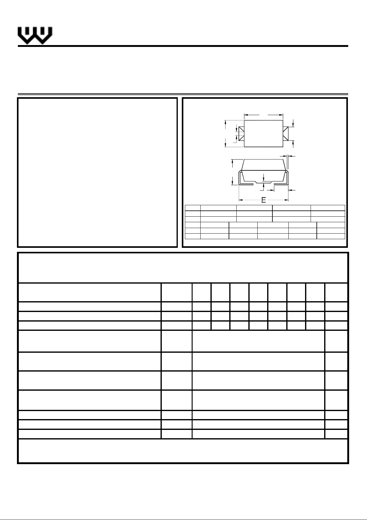
.110(2.79
.100(2.54).157(3.99
MIN.
.208(5.28
.194(4.93).078(1.98
MIN.
Dimensions in inches and (millimeters
TECHNICAL
SPECIFICATION
DSMA/DO-214AC
B
A
I
F
G
A
EFGHI
.090(2.29
B
.177(4.50
.008(0.203
.004(0.102).030(0.76
C
D
H
C
.075(1.90
.052(1.32
.060(1.52
D
.012(0.305
.006(0.152
.035(0.88
.027(0.68
MAXIMUM RATINGS AND ELECTRICAL CHARACTERISTICS
(Single-phase, half-wave, 60Hz, resistive or inductive load rating at 25oC, unless otherwise stated, for capacitive load,
derate current by 20%)
RATINGS
Maximum Repetitive Peak Reverse Voltage
Maximum RMS Voltage
Maximum DC Blocking Voltage
Maximum Average Forward Rectified Current
(T
=100oC)
L
Peak Forward Surge Current (8.3ms single
half sine-wave superimposed on rated load)
Maximum Instantaneous Forward Voltage
(at rated forward current)
Maximum DC Reverse Current
(at rated DC blocking voltage)
T
=25oC
a
=125oC
T
a
Typical Junction Capacitance (Note 1)
Typical Thermal Resistance (Note 2)
Storage and Operation Junction Temperature
Note:
1.Measured at 1.0 MHz and applied voltage of 4.0V
2.Thermal resistance from junction to terminal mounted on 5×5mm copper pad area
SYMBOL M1 M2 M3 M4 M5 M6 M7 UNITS
V
RRM
V
RMS
V
I
F(AV)
I
FSM
V
I
C
R
θ
T
STG,TJ
DC
F
R
J
(ja)
dc
50 100 200 400 600 800 1000 V
35 70 140 280 420 560 700 V
50 100 200 400 600 800 1000 V
1.0 A
30 A
1.1 V
5.0
200
15
27
-65 to +150
µA
µA
pF
o
C/W
o
C
http://www.sse-diode.com
 Loading...