

PRODUCT SELECTION GUIDE
PARAMETER WS57LV291C-70 WS57LV291C-90
Address Access Time (Max) 70 ns 90 ns
CS to Output Valid Time (Max) 20 ns 30 ns
HIGH SPEED 3.3 VOLT 2K x 8 CMOS PROM/RPROM
KEY FEATURES
• 3.3 Volt ± 0.3 Volt V
CC
• Available in 300 Mil "Skinny" DIP
• Fast Access Time • Immune to Latch-up
— t
ACC
= 70 ns — Up to 200 mA
—tCS= 20 ns
• ESD Protection Exceeds 2000V
• Low Power Consumption
— ≤ 25 mA I
CC
GENERAL DESCRIPTION
The WS57LV291C is a High Performance 2K x 8 UV Erasable Re-Programmable Read Only Memory (RPROM).
This RPROM is manufactured using an advanced CMOS EPROM manufacturing process resulting in a very low
power die that affords exceptional speed capabilities with a 3.3 volt VCCsupply. The WS57LV291C
is configured in the standard Bipolar PROM pinouts, the preferred and most common pinout for high speed PROMs
of 16K density.
Operating at 3.3 volts, the WS57LV291C dissipates a maximum of 25 mA under worst case conditions at maximum
speed (70 ns TAA). Typical ICCat 25°C is less than 20 milliamps.
The WS57LV291C is packaged in a space saving 300 mil windowed, hermetic DIP package.
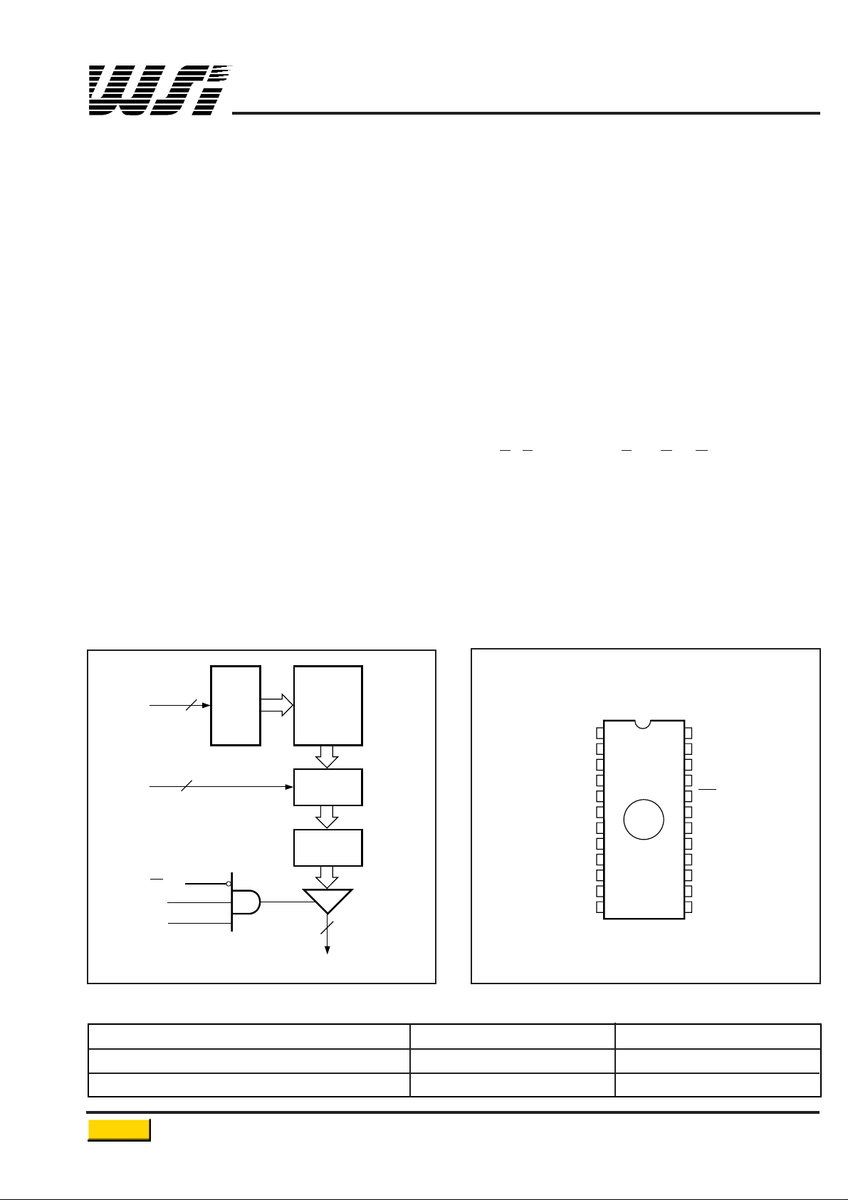
WS57LV291C
V
CC
A
8
A
9
A
10
CS1/V
PP
CS2
CS3
O
7
O
6
O
5
O
4
O
3
A
7
A
6
A
5
A
4
A
3
A
2
A
1
A
0
O
0
O
1
O
2
GND
1
2
3
4
5
6
7
8
9
10
11
12
24
23
22
21
20
19
18
17
16
15
14
13
TOP VIEW
CERDIP
PRELIMINARY
PIN CONFIGURATION
2-15
ROW
DECODER
EPROM ARRAY
16,384 BITS
COLUMN
DECODER
SENSE
AMPLIFIERS
8
CS2
CS3
OUTPUTS
CS1/V
PP
A0 - A4
COLUMN
ADDRESSES
A5 - A10
ROW
ADDRESSES
6
5
BLOCK DIAGRAM
Return to Main Menu
AC READ CHARACTERISTICS
Over Operating Range. (See Above)
PARAMETER SYMBOL
WS57LV291C-70 WS57LV291C-90
UNITS
MIN MAX MIN MAX
Address to Output Delay t
ACC
70 90
CS to Output Delay t
CS
20 30
ns
Output Disable to Output Float* t
DF
20 30
Address to Output Hold t
OH
00
WS57LV291C
2-16
DC READ CHARACTERISTICS
Over Operating Range. (See Above)
SYMBOL PARAMETER TEST CONDITIONS MIN MAX UNITS
V
IL
Input Low Voltage (Note 3) –0.1 0.6 V
V
IH
Input High Voltage (Note 3) 2.0 V
CC
+ 0.3 V
V
OL
Output Low Voltage IOL= 16 mA 0.4 V
V
OH
Output High Voltage IOH= –4 mA 2.4 V
(Notes 1 and 2)
I
CC
VCCActive Current (CMOS) I
CC
at Maximum Frequency 25 mA
Outputs Not Loaded
I
LI
Input Leakage Current VIN= 3.6V or Gnd –10 10 µA
I
LO
Output Leakage Current V
OUT
= 3.6 V or Gnd –10 10 µA
OPERATING RANGE
RANGE TEMPERATURE V
CC
Commercial 0°C to +70°C + 3.3V ± 0.3V
ABSOLUTE MAXIMUM RATINGS*
Storage Temperature............................–65° to + 150°C
Voltage on any Pin with
Respect to Ground ....................................–0.6V to +7V
VPPwith Respect to Ground...................–0.6V to + 14V
ESD Protection..................................................>2000V
NOTES: 1. CMOS inputs: GND ± 0.3V or VCC± 0.3V.
2. For TTL inputs
add 5 mA ICC.
3. These are absolute voltages with respect to device ground pin and include all overshoots due to system and/or tester noise.
Do not attempt to test these values without suitable equipment.
*
NOTICE:
Stresses above those listed under "Absolute Maximum
Ratings" may cause permanent damage to the device.
This is a stress rating only and functional operation of
the device at these or any other conditions above
those indicated in the operational sections of this
specification is not implied. Exposure to absolute
maximum rating conditions for extended periods of
time may affect device reliability.
*Sampled, Not 100% Tested.
MODE
PINS CS1/
CS2 CS3 V
CC
OUTPUTS
V
PP
Read V
IL
V
IH
V
IHVCC
D
OUT
Output
Disable
V
IH
XXVCCHigh Z
Output
XVILXVCCHigh Z
Disable
Output
Disable
XXVILV
CC
High Z
Program V
PP
XXVCCD
IN
Program
Verify
V
IL
V
IH
V
IHVCC
D
OUT
MODE SELECTION

SYMBOL PARAMETER CONDITIONS TYP
(5)
MAX UNITS
C
IN
Input Capacitance VIN= 0V 4 6 pF
C
OUT
Output Capacitance V
OUT
= 0V 8 12 pF
C
VPP
VPPCapacitance VPP= 0 V 18 25 pF
2-17
WS57LV291C
AC READ TIMING DIAGRAM
VALID
ADDRESSES
OUTPUTS
t
ACC
t
OH
t
CS
t
DF
VALID
CS
CAPACITANCE
(4)
TA= 25°C, f = 1 MHz
30 pF
(INCLUDING SCOPE
AND JIG
CAPACITANCE)
98 Ω
1.80 V
D.U.T.
A.C. TESTING INPUT/OUTPUT WAVEFORMTEST LOAD
(High Impedance Test Systems)
3.0
0.0
1.5 1.5
TEST
POINTS
NOTE: 6. Provide adequate decoupling capacitance as close as possible to this device to achieve the published A.C. and D.C. parameters.
A 0.1 microfarad capacitor in parallel with a 0.01 microfarad capacitor connected between VCCand ground is recommended.
Inadequate decoupling may result in access time degradation or other transient performance failures.
NOTES: 4. This parameter is only sampled and is not 100% tested.
5. Typical values are for TA= 25°C and nominal supply voltages.
A.C. testing inputs are driven at 3.0 V for a logic "1" and 0.0 V for a
logic "0." Timing measurements are made at 1.5 V for input and
output transitions in both directions.

WS57LV291C
2-18
1.2
1.1
1.0
0.9
0.8
-55 -35 -15 5 25 45 65 85 105 125
AMBIENT TEMPERATURE (°C)
NORMALIZED I
CC
1.60
1.40
1.20
1.00
0.80
0.60
4.0 4.5 5.0 5.5 6.0
SUPPLY VOLTAGE (V
)
NORMALIZED I
CC
1.6
1.4
1.2
1.0
0.8
0.6
-55 -35 -15 5 25 45 65 85 105 125
AMBIENT TEMPERATURE (°C
)
NORMALIZED T
aa
40.0
35.0
30.0
25.0
20.0
15.0
10.0
5.0
0.0
0.0 200 400 600 800 1000
CAPACITANCE (pF
)
DELTA T
aa
(
ns
)
NORMALIZED SUPPLY CURRENT
vs.
SUPPLY VOLTAGE
TYPICAL ACCESS TIME CHANGE
vs.
OUTPUT LOADING
NORMALIZED T
aa
vs.
AMBIENT TEMPERATURE
NORMALIZED SUPPLY CURRENT
vs.
AMBIENT TEMPERATURE

PROGRAMMING INFORMATION
DC CHARACTERISTICS
(TA= 25 ± 5°C, VCC= 6.25 V ± 0.25 V, VPP= 12.75 ± 0.25 V)
SYMBOLS PARAMETER MIN MAX UNITS
I
LI
Input Leakage Current
–10 10 µA
(VIN= VCCor Gnd)
I
PP
VPPSupply Current During
60 mA
Programming Pulse
I
CC
VCCSupply Current 25 mA
V
OL
Output Low Voltage During Verify
0.45 V
(IOL= 16 mA)
V
OH
Output High Voltage During Verify
2.4 V
(IOH= –4 mA)
2-19
WS57LV291C
SYMBOLS PARAMETER MIN TYP MAX UNITS
t
AS
Address Setup Time 2 µs
t
DF
Chip Disable Setup Time 30 ns
t
DS
Data Setup Time 2 µs
t
PW
Program Pulse Width 100 200 µs
t
DH
Data Hold Time 2 µs
t
CS
Chip Select Delay 30 ns
t
RF
VPPRise and Fall Time 1 µs
NOTES: 7. V
PP
must not be greater than 13 volts including overshoot.
AC CHARACTERISTICS
(TA= 25 ± 5°C, VCC= 6.25 V ± 0.25 V, VPP= 12.75 ± 0.25 V)
PROGRAMMING WAVEFORM
ADDRESS STABLE
ADDRESSES
V
IH
V
IL
V
PP
V
IH
V
IH
V
IL
V
IL
CS1/V
PP
DATA
t
AS
t
DF
t
DS
t
PW
t
DH
t
CS
t
RF
t
RF
DATA OUTDATA IN
DON'T CARE
CS2/CS3
V
IH
V
IL
WS57LV291C
2-20
ORDERING INFORMATION
SPEED PACKAGE PACKAGE
OPERATING WSI
PART NUMBER
(ns) TYPE DRAWING
TEMPERATURE MANUFACTURING
RANGE PROCEDURE
WS57LV291C-70T 70 24 Pin CERDIP, 0.3" T1 Comm’l Standard
WS57LV291C-90T 90 24 Pin CERDIP, 0.3" T1 Comm’l Standard
NOTE: 8. The actual part marking will not include the initials "WS."
PROGRAMMING/ALGORITHMS/ERASURE/PROGRAMMERS
REFER TO
PAGE 5-1
The WS57LV291C is programmed using Algorithm D shown on page 5-9.
Return to Main Menu
 Loading...