SGS Thomson Microelectronics WS57C49C Datasheet

WS57C49C
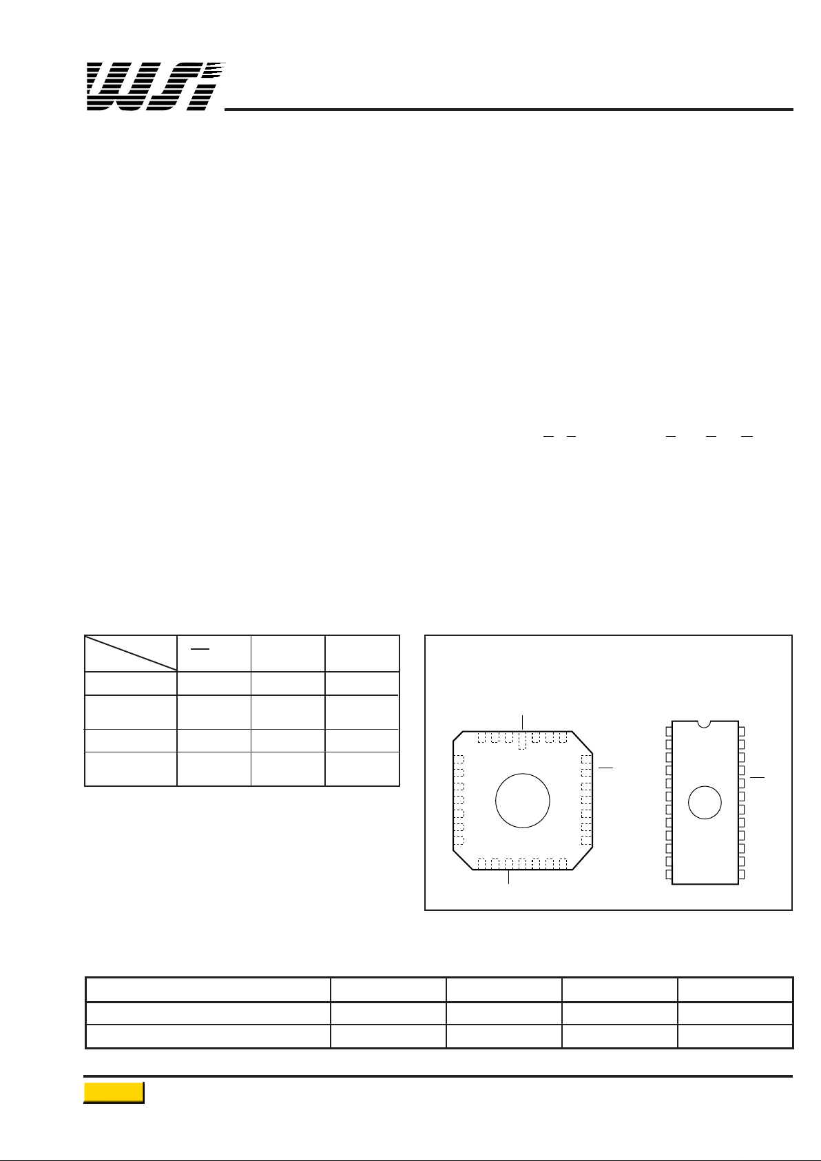
MODE
PINS
CS1/V
PP
V
CC
OUTPUTS
Read V
IL
V
CC
D
OUT
Output
Disable
V
IH
V
CC
High Z
Program V
PP
V
CC
D
IN
Program
Verify
V
IL
V
CC
D
OUT
V
CC
A
8
A
9
A
10
CS1/V
PP
A
11
A
12
O
7
O
6
O
5
O
4
O
3
A
7
A
6
A
5
A
4
A
3
A
2
A
1
A
0
O
0
O
1
O
2
GND
A
10
CS1/V
PP
A
11
A
12
NC
O
7
O
6
A5 A6 A7 VCC A8 A
9
NC
A
4
A
3
A
2
A
1
A
0
NC
O
0
O1 O2 NC O3 O4 O
5
GND
1
2
3
4
5
6
7
8
9
10
11
12
24
23
22
21
20
19
18
17
16
15
14
13
1
432
28 27
26
25
24
23
22
21
20
19
5
6
7
8
9
10
11
12 13 1415161718
TOP VIEW
Chip Carrier CERDIP/Flatpack
MODE SELECTION PIN CONFIGURATION
4-9
MILITARY HIGH SPEED 8K x8 CMOS PROM/RPROM
KEY FEATURES
• Ultra-Fast Access Time • Pin Compatible with Bipolar PROMs
— t
ACC
= 35 ns
• Immune to Latch-UP
— tCS= 20 ns
— Up to 200 mA
• Low Power Consumption
• ESD Protection Exceeds 2000 V
• Fast Programming
• Available in 300 and 600 Mil DIP, CLLCC,
and Flatpack
GENERAL DESCRIPTION
The WS57C49C is a High Performance 64K UV Erasable Electrically Re-Programmable Read Only Memory
(RPROM). It is manufactured in an advanced CMOS technology which enables it to operate at Bipolar PROM
speeds while consuming only 25% of the power required by its Bipolar counterparts. A further advantage of the
WS57C49C over Bipolar PROM devices is the fact that it utilizes a proven EPROM technology. This enables the
entire memory array to be tested for switching characteristics and functionality after assembly. Unlike devices which
cannot be erased, every WS57C49C in a windowed package is 100% tested with worst case test patterns both
before and after assembly.
The WS57C49C is configured in the standard Bipolar PROM pinout which provides an easy upgrade path for
systems which are currently using Bipolar PROMs, or its predecessor, the WS57C49B.
PRODUCT SELECTION GUIDE
PARAMETER WS57C49C-35 WS57C49C-45 WS57C49C-55 WS57C49C-70
Address Access Time (Max) 35 ns 45 ns 55 ns 70 ns
CS to Output Valid Time (Max) 20 ns 25 ns 25 ns 25 ns
Return to Main Menu

WS57C49C
4-10
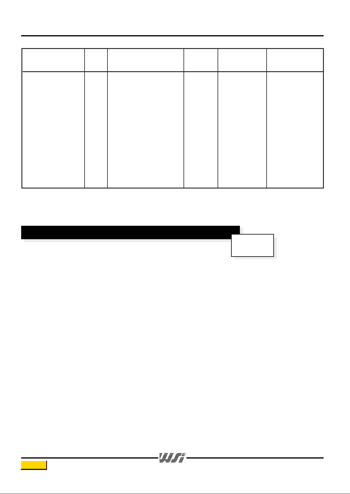
ORDERING INFORMATION
OPERATING WSI
PART NUMBER TEMPERATURE MANUFACTURING
RANGE PROCEDURE
WS57C49C-35CMB* 35 28 Pad CLLCC C1 Military MIL-STD-883C
WS57C49C-35TMB* 45 24 Pin CERDIP, 0.3" T1 Military MIL-STD-883C
WS57C49C-35DMB 45 24 Pin CERDIP, 0.6" D1 Military MIL-STD-883C
WS57C49C-45CMB* 45 28 Pad CLLCC C1 Military MIL-STD-883C
WS57C49C-45DMB* 45 24 Pin CERDIP, 0.6" D1 Military MIL-STD-883C
WS57C49C-45TMB* 45 24 Pin CERDIP, 0.3" T1 Military MIL-STD-883C
WS57C49C-55CMB* 55 28 Pad CLLCC C1 Military MIL-STD-883C
WS57C49C-55DMB* 55 24 Pin CERDIP, 0.6" D1 Military MIL-STD-883C
WS57C49C-55FMB* 55 24 Pin Ceramic Flatpack F1 Military MIL-STD-883C
WS57C49C-55TMB* 55 24 Pin CERDIP, 0.3" T1 Military MIL-STD-883C
WS57C49C-70CMB* 70 28 Pad CLLCC C1 Military MIL-STD-883C
WS57C49C-70TMB* 70 28 Pin CERDIP, 0.3" T1 Military MIL-STD-883C
SPEED PACKAGE PACKAGE
(ns) TYPE DRAWING
PROGRAMMING/ALGORITHMS/ERASURE/PROGRAMMERS
REFER TO
PAGE 5-1
The WS57C49C is programmed using Algorithm D shown on page 5-9.
NOTE: The actual part marking will not include the initials "WS."
*SMD product. See page 4-1 for DESC SMD numbers.
For complete data sheet and electrical specifications see page 2-39.
Return to Main Menu
 Loading...