

SGS Thomson Microelectronics VNS14NV04, VND14NV04, VND14NV04-1, VNP14NV04, VNB14NV04 Datasheet

®
VNB14NV04 / VND14NV04
3
VND14NV0 4-1 / VNP14N V0 4 / VNS14N V0 4
/
“OMNIFE T II” :
FULLY AUTOPROTECTED POWER MOSFET
TYPE R
DS(on)
I
lim
V
clamp
VNB14NV04
VND14NV04
VND14NV04-1
35 mΩ 12 A 40 V
VNP14NV04
VNS14NV04
■ LINEAR CURRENT LIMITATION
■ THERM AL SHUT DOWN
■ SHORT CIRCUIT PROTECTION
■ INTEGRATED CLAMP
■ LOW CURRENT DRAWN FROM INPUT PIN
■ DIAGNOSTIC FEEDBACK THROUGH INPUT
PIN
■ ESD PROTECTION
■ DIRECT ACCESS TO THE GATE OF THE
POWER MOSFET (ANALOG DRIVING)
■ COMPATIBLE WI TH STANDARD POWER
MOSFET
DESCRIPTION
The VNB14NV04, VND14NV04, VND14NV04-1,
VNP14NV04, VNS14NV04, are monolithic
devices de signed in ST Microelect ronics VIPo wer
M0-3 Technology, intended for replacement of
standard Power MOSFETS from DC up to 50KHz
BLO C K DIAGRA M
3
1
SO-8TO-252 (DPAK)
3
2
1
TO-220 TO-251 (IPAK)
2
1
D2PAK
3
1
ORDER CODES
PACKAGE TUBE T&R
2
PAK VNB14NV04 VNB14NV0413TR
D
TO-252 (DPAK) VND14NV04 VND14NV0413TR
TO-251 (IPAK) VND14NV04-1 TO-220 VNP14NV04
SO-8 VNS14NV04
-
-
applications. Built in thermal shutdown, linear
current limitation |and overvoltage clamp protect
the chip in harsh environments.
Fault feedback can be detected by monitoring the
voltage at the input pin.
DRAIN
2
Overvoltage
Clamp
INPUT
1
Gate
Control
Over
Temperature
Linear
Current
Limiter
3
SOURCE
July 2003 1/29
1
VNB14NV04 / VND14NV04 / VND14NV04-1 / VNP14NV04 / VNS14NV04
ABSOLUTE MAXIMUM RATI NG
Symbol Parameter
Drain-source Voltage (VIN=0V) Internally Clamped V
DS
Input Voltage Internally Clamped V
V
IN
Input Current +/-20 mA
I
IN
Minimum Input Series Impedance 10 Ω
Drain Current Internally Limited A
I
D
Reverse DC Output Current -15 A
I
R
Electros tatic Discharge (R=1.5KΩ, C=100p F) 4000 V
ESD1
Electros tatic Discharge on output pin only
ESD2
(R=330 Ω, C=150pF)
Total Dissipation at Tc=25°C 4.6 74 74 74 74 W
P
tot
Maximum Swi tching Energy (L=0.4 m H;
MAX
RL=0Ω; V
Operating Junction Tem perature Internally limited °C
T
j
Case Oper ating Tempe rature Internally limited °C
T
c
Storage Temperature -55 to 150 °C
stg
=13.5V; T
bat
=150ºC; IL=18A)
jstart
R
V
V
E
V
IN MIN
T
CONNECTION DIAGRAM (TOP VIEW)
SO-8 DPAK TO-220 IPAK D
93 93 mJ
SO-8 Package (*)
Value
16500 V
2
PAK
Unit
SOURCE
SOURCE
SOURCE
INPUT
(*) For the pins configuration related to DPAK, D2PAK, IPAK, TO-220 see outlines at page 1.
1
4
CURRENT AND VOLTAGE CONVENTIONS
I
IN
R
IN
INPUT
SOURCE
V
IN
8
5
DRAIN
DRAIN
DRAIN
DRAIN
DRAIN
I
D
V
DS
2/29
1
VNB14NV04 / VND14NV04 / VND14NV04-1 / VNP14NV04 / VNS14NV04
THERMAL DATA
Symbol Parameter
R
thj-case
R
thj-lead
R
thj-amb
(*) When mounted on a standar d s ingle-sided FR4 board wit h 0.5cm
Horizontal mounting and no artificial air flow.
Thermal R esistance Junction- case MAX 1.7 1.7 1 .7 1.7 °C/W
Thermal Resistance Junction-lead MAX 27 °C/W
Thermal R esistance Junction- am bient MAX 90 (*) 65 (*) 62 102 52 (*) ° C/W
SO-8 DPAK TO-220 IPAK D
2
of Cu (at least 35 µm thick) connected to all DRAIN pins.
ELECTRICAL CHARACTERISTICS (-40°C < Tj < 150°C, unless otherwise specified)
OFF
Symbol Parameter Test Conditi ons Min Typ Max Unit
V
CLAMP
V
CLTH
V
INTH
I
V
INCL
I
DSS
ISS
Drain-source Clamp
Voltage
Drain-source Clamp
Threshold Voltage
Input Thre shold Volta ge VDS=VIN; ID=1mA 0.5 2.5 V
Supply Current from Input
Pin
Input-Source Clamp
Voltage
Zero Input Voltage Drai n
Current (VIN=0V)
V
=0V; ID=7A 40 45 55 V
IN
=0V; ID=2mA 36 V
V
IN
VDS=0V; VIN=5V 100 150 µA
IIN=1mA
I
=-1mA
IN
V
=13V; VIN=0V; Tj=25°C
DS
V
=25V; VIN=0V
DS
Value
-1.0
2
PAK
6
6.8 8
-0.3
30
75
Unit
V
µA
ON
Symbol Parameter Test Conditi ons Min Typ Max Unit
V
R
DS(on)
Static Drain-source On
Resistance
=5V; ID=7A; Tj=25°C
IN
V
=5V; ID=7A
IN
35
70
mΩ
3/29
1
VNB14NV04 / VND14NV04 / VND14NV04-1 / VNP14NV04 / VNS14NV04
ELECTRICAL CHARACTERISTICS (continued) (Tj=25°C, unless otherwise specified)
DYNAMIC
Symbol Parameter Test Condi tions Min Ty p Max Unit
gfs (*)
C
OSS
SWITCHING
Symbol P arameter Test Co nditions Min Typ Max Unit
t
d(on)
t
t
d(off)
t
t
d(on)
t
t
d(off)
t
(di/dt)
Q
Forward
Transconductance
VDD=13V; ID=7A 18 S
Output Ca pacitance VDS=13V; f=1MHz; VIN=0V 400 pF
Turn-on Delay Time
Rise Time 350 1000 ns
r
Turn-off Delay Time 450 1350 ns
Fall Time 150 500 ns
f
Turn-on Delay Time
Rise Time 9.7 30.0 µs
r
Turn-off Delay Time 9 25.0 µs
Fall Time 10.2 30.0 µs
f
Turn-on Current Slope
on
Total Input Charge
i
=15V; ID=7A
V
DD
V
=5V; R
gen
gen=RIN MIN
(see figure 1)
=15V; ID=7A
V
DD
V
gen
=5V; R
gen
=2.2K Ω
(see figure 1)
=15V; ID=7A
V
DD
V
=5V; R
gen
V
DD
gen=RIN MIN
=12V; ID =7A; VIN=5V; I
(see figure 5)
=10Ω
=10Ω
=2.13m A
gen
80 250 ns
1.5 4.5 µs
16 A/µs
36.8 nC
SOURCE DRAIN DIODE
Symbol Parameter Test Conditions Min Typ Max Unit
(*) For ward On Voltag e ISD =7A; VIN=0V 0.8 V
V
SD
Q
I
RRM
t
Reverse Recovery Time ISD=7A; di/dt=4 0A/µs
rr
Reverse Recovery Charge 0.8 µC
rr
Reverse Recovery Current 5 A
V
=30V; L= 20 0 µ H
DD
(see test circuit, figure 2)
300 ns
PROTECTIONS (-40°C < Tj < 150°C, unless otherwise specified)
Symbol Parameter Test Conditions Min Typ Max Unit
I
lim
t
dlim
T
jsh
T
I
gf
E
(*) Pulsed: Pu ls e duration = 300µs, dut y c y c le 1.5%
Drain Current Limit VIN=5V; VDS=13V 12 18 24 A
=5V; VDS=13V
Step Response Current
Limit
Overtemperature
Shutdown
Overtemperature Reset 135 °C
jrs
Fault Sink Current VIN=5V; VDS=13V; Tj=T
Sing l e Pu lse
as
Avala nche Energy
V
IN
starti ng T
V
IN
= 5V; R
=25°C; V
j
gen=RIN MIN
(see figures 3 & 4)
jsh
=24V
DD
=10Ω; L=24mH
45 µs
150 175 200 °C
10 15 20 mA
400 mJ
4/29
2

VNB14NV04 / VND14NV04 / VND14NV04-1 / VNP14NV04 / VNS14NV04
PROTECTION FEATURES
During normal operation, the INPUT pin is
electrically connected to the gate of the internal
power MOSFET through a low impedance path.
The device then behaves like a standard power
MOSFET and can be used as a switch from DC up
to 50KHz. The only difference from the user’s
standpoint is that a small DC current I
100µA) flows into the INPUT pin in order to supply
ISS
(typ.
the internal circuitry.
The de vice integrates:
- OVERVOLTAGE CLAMP PROTECTION:
internally set at 45V, along with the rugged
avalanche characteristics o f the Power MOSFET
stage giv e this device unrivall ed ruggedne ss and
energy handl ing capability. This feat ure is mainly
important when driving inductive loads.
- LINEAR CURRENT LIMITER CIRCUIT:
limits the drain current ID to I
INPUT pin voltages. When the current limiter is
whatever the
lim
active, the device operates in the linear region, so
power dissipation may exceed the capability of the
heatsink. Both case and junction temperatures
increase, and if this phase lasts long enough,
junction temperature may reach the
overtemperature threshold T
jsh
.
- OVERTEMPERATURE AND SHORT CIRCUIT
PROTECTION:
these are based on sensing the chip t emperatur e
and are not dependen t on the input voltage. The
location o f t he s ensing el emen t on the c h ip i n t he
power stage area ensures fast, accurate detection
of the junction temperature. Overtemperature
cutout occurs in the range 150 to 190 °C, a typical
value being 170 °C. The device is auto matically
restarted when the chip temp eratu re fall s of about
15°C below shut-down temperature.
- STATUS FEEDBACK:
in the case of an overtem perature fault cond ition
(Tj > T
current Igf through the INPUT pin in order to
), the device tries to sink a diagnostic
jsh
indicate fault condition. If driven from a low
impedance source, this current may be used in
order to warn the control circuit of a device
shutdown. If the drive imped ance is high enough
so that the INPUT p in dri ver is no t abl e to su pply
the current Igf, the INPUT pin will fall to 0V. This
will not however affect the device operation:
no requirement is put on the current capability
of the INPUT pin driver except to be able to
supply the normal operation drive current I
ISS
Additional features of this device are ESD
protection according to the Human Body model
and the ability to be driven from a TTL Logic
circuit.
.
5/29
VNB14NV04 / VND14NV04 / VND14NV04-1 / VNP14NV04 / VNS14NV04
Figure 1: Switching Time Test Circuit for Resistive L oad
V
D
R
gen
V
gen
I
D
90%
t
r
t
V
gen
d(on)
10%
Figure 2: Test Circuit for Diode Recovery Times
A
D
I
OMNIFET
S
25 Ω
B
R
FAST
DIODE
gen
t
d(off)
I
OMNIFET
t
f
t
t
A
L=100uH
B
D
V
DD
6/29
V
gen
S
8.5 Ω
VNB14NV04 / VND14NV04 / VND14NV04-1 / VNP14NV04 / VNS14NV04
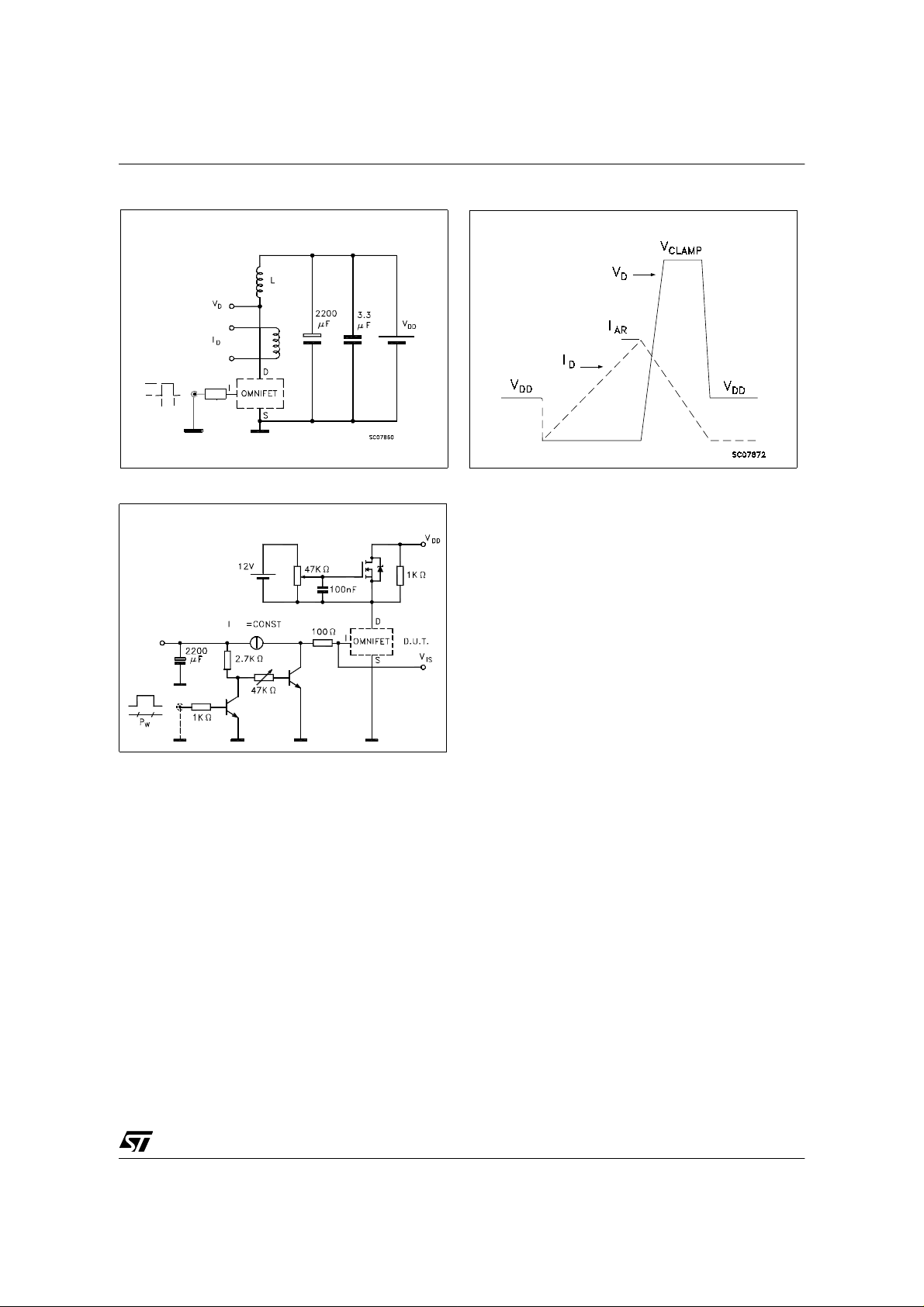
Figure 3: Unclamped Inductive Load Test Circuits
R
V
IN
P
GEN
W
Figure 5: Input Charge Test Circuit
IN
V
GEN
Figure 4: Unclamped Inductive Waveforms
ND8003
7/29

VNB14NV04 / VND14NV04 / VND14NV04-1 / VNP14NV04 / VNS14NV04
Source-Drain Diode Forward Characteristics
Vsd (mV)
1000
950
900
850
800
750
700
650
Vin=0V
0 2 4 6 8 10 12 14 16 18
Id (A)
Derating Curve
Static Drain Source On Resistance
Rds(on) (mohms)
180
160
140
120
100
80
60
40
20
Vin=2.5V
0.1 0.2 0.3 0.4 0.5 0.6 0.7 0.8 0.9 1
Tj=-40ºC
Tj=25ºC
Tj=150ºC
Id(A)
Static Drain-Source On resistance Vs. Input
Voltage
Rds(on) (mohms)
80
70
Tj=150ºC
60
50
Tj=25ºC
40
Id=12A
Id=1A
Static Drain-Source On resistance Vs. Input
Voltage
Rds(on) (mohms)
80
70
60
50
40
30
20
10
33.544.555.566.5
Vin(V)
8/29
Id=7A
Tj=150ºC
Tj=25ºC
Tj= - 40ºC
30
Tj=-40ºC
20
10
3 3.5 4 4.5 5 5.5 6 6.5
Vin(V)
Transconductance
Gfs (S)
24
22
Vds=13V
20
18
16
14
12
10
8
6
4
2
0
012345678910111213
Tj=-40ºC
Tj=150ºC
Id(A)
Id=12A
Id=1A
Id=12A
Id=1A
Tj=25ºC

VNB14NV04 / VND14NV04 / VND14NV04-1 / VNP14NV04 / VNS14NV04
Static Drain-Source On Resistance Vs. Id
Rds(on) (mohms)
70
60
Vin=5V
50
40
30
20
10
0
012345678910111213
Tj=150ºC
Tj=25ºC
Tj=-40ºC
Id(A)
Turn On Current Slope
di/dt(A/us)
20
17.5
15
12.5
10
7.5
5
2.5
0
0 250 500 750 1000 1250 1500 1750 2000 2250
Rg(ohm)
Vin=5V
Vdd=15V
Id=7A
Transfer Characteristics
Idon (A)
18
16
14
12
10
8
6
4
2
0
2
Vds=13.5V
Tj=150ºC
2.25
2.5
2.7533.25
3.5
3.7544.25
Vin (V)
Turn On Current Slope
di/dt(A/us)
6
5.5
5
4.5
4
3.5
3
2.5
2
1.5
1
0.5
0
0 250 500 750 1000 1250 1500 1750 2000 2250
Rg(ohm)
4.5
4.7555.25
Vin=3.5V
Vdd=15V
Id=7A
Tj=25ºC
Tj=-40ºC
5.5
Input Voltage Vs. Input Charge
Vin (V)
8
7
6
5
4
3
2
1
0
Vds=12V
Id=7A
0 5 10 15 20 25 30 35 40 45
Qg (nC)
Turn off drain source voltage slope
dv/dt(V/us)
300
275
250
225
200
175
150
125
100
75
50
25
0
0
500
250
750
1000
1250
Rg(ohm)
1500
1750
Vin=5V
Vdd=15V
Id=7A
2000
2250
2500
9/29
 Loading...