

M
®
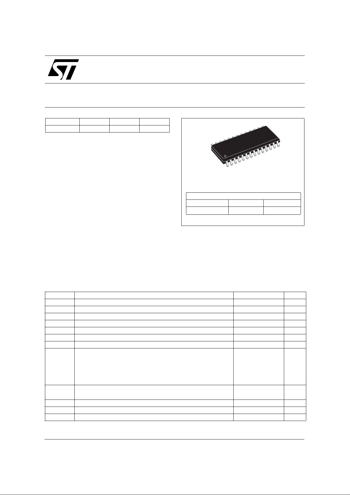
VNQ830
QUAD C HAN NEL HI GH SI DE DRIV ER
TYPE R
DS(on)
I
OUT
V
CC
VNQ830 65 mΩ (*) 6 A (*) 36 V
(*) Per each channel
■ CMOS COMPATIBLE INPUTS
■ OPEN DRAIN STATUS OUTPUTS
■ ON STATE OPEN LOAD DETECTION
■ OFF STATE OPEN LOAD DETECTION
■ SHORTED LOAD PROTECTION
■ UNDERVOLTAGE AND OVERVOLTAGE
SO-28 (DOUBLE ISLAND)
SHUTDOWN
■ LOSS OF GROUND PROTECTION
■ VERY LOW STAND-BY CURRENT
■ REVERSE BA TTERY PROTECTION (**)
PACKAGE TUBE T&R
SO-28
ORDER CODES
VNQ830 VNQ83013TR
DESCRIPTION
The VNQ830 is a quad HSD formed by
assembling two VND830 chi ps in the same SO-28
package. The VND830 is a monolithic device
made by using| STMicroelectronics VIPower M0-3
Technology. The VNQ830 is intend ed for driving
any type of multiple loads with one side connected
to ground.
Active VCC pin voltage clamp protects the device
against low energy spikes (see ISO7637 transient
compatibility table). Active current limitation
combined with thermal shu tdown and automatic
restart protects the device against overload.
The device detects open load condition both in on
and off state. Output shorted to VCC is det e c ted i n
the off state. Device automatically turns off in case
of ground pin disconnection.
ABSOLUTE MAXIMUM RATI NG
Symbol Parameter Value Unit
tot
DC Supply Vol tage 41 V
Reverse DC Supply Voltage - 0.3 V
CC
DC Reverse Ground Pin Curr ent - 200 mA
DC Output Current Internally Limited A
Reverse DC Output Current - 6 A
DC Input Cur rent +/- 10 mA
DC Status Cur rent +/- 10 mA
Electros tatic Disc harge (Huma n Body Model: R=1.5KΩ; C=100pF)
- INPU T
- STATUS
- OUTPU T
- V
CC
Maximum Swi tching Energy
(L=1.5mH; R
Power dissipation (per isla nd) at T
Junction Operating Tempera ture Internally Limi ted °C
j
=0Ω; V
L
=13.5V; T
bat
=150ºC; IL=9A)
jstart
=25°C 6.25 W
lead
4000
4000
5000
5000
85 mJ
Storage Temperature - 55 to 150 °C
V
CC
- V
- I
GND
I
OUT
- I
OUT
I
IN
I
STAT
V
ESD
E
MAX
P
T
T
stg
(**) See appl ic ation schematic at page 9
V
V
V
V
Janua ry 20 03 1/20

VNQ830
BLOCK DIAGRAM
V
cc
CLAMP
OVERVOLTAGE
UNDERVOLTAGE
V
CC1,2
GND1,2
INPUT1
STATUS1
INPUT2
STATUS2
GND3,4
INPUT3
STATUS3
INPUT4
STATUS4
OVERTEMP. 1
OVERTEMP. 2
V
cc
CLAMP
OVERTEMP. 3
LOGIC
LOGIC
CLAMP 1
DRIVER 1
CURRENT LIMITER 1
OPENLOAD ON 1
OPENLOAD OFF 1
OVERVOLTAGE
UNDERVOLTAGE
CLAMP 3
DRIVER 3
CURRENT LIMITER 3
OPENLOAD ON 3
OPENLOAD OFF 3
CLAMP 2
DRIVER 2
CURRENT LIMITER 2
OPENLOAD ON 2
OPENLOAD OFF 2
CLAMP 4
DRIVER 4
CURRENT LIMITER 4
OPENLOAD ON 4
OUTPUT1
OUTPUT2
V
CC3,4
OUTPUT3
OUTPUT4
2/20
OVERTEMP. 4
OPENLOAD OFF 4

CURRENT AND VOLTAGE CONVENTIO N S
VNQ830
I
S1,2
V
CC1,2
I
IN1
STAT3
V
IN4
V
STAT4
I
STAT1
I
IN2
I
STAT2
I
IN3
I
STAT3
I
IN4
I
STAT4
V
IN1
V
STAT1
V
IN2
V
STAT2
V
IN3
V
CONNECTION DIAG R A M (TOP VIE W )
VCC1,2
GND 1,2
INPUT1
STATUS1
STATUS2
INPUT2
V
1,2
CC
V
3,4
CC
GND 3,4
INPUT3
STATUS3
STATUS4
INPUT4
3,4
V
CC
V
CC1,2
INPUT1
STATUS1
INPUT2
STATUS2
INPUT3
STATUS3
INPUT4
STATUS4
GND
1
14 15
1,2
I
GND1,2
V
CC3,4
OUTPUT1
OUTPUT2
OUTPUT3
OUTPUT4
GND
28
3,4
I
GND3,4
I
OUT1
I
OUT2
I
OUT3
V
OUT3
I
OUT4
V
OUT4
V
1,2
CC
OUTPUT1
OUTPUT1
OUTPUT1
OUTPUT2
OUTPUT2
OUTPUT2
OUTPUT3
OUTPUT3
OUTPUT3
OUTPUT4
OUTPUT4
OUTPUT4
V
3,4
CC
I
S3,4
V
OUT2
V
OUT1
V
CC3,4
3/20
VNQ830
THERMAL DATA (Per island)
Symbol Parameter Value Unit
R
thj-lead
R
thj-amb
R
thj-amb
(*) When mounted on a standard si ngle-sided FR-4 board with 0.5c m2 of Cu per island (at least 35µm thick) connected to all VCC pins.
Horizontal mounting and no artificial air flow.
ELECTRICAL CHARACTERISTICS (8V<VCC<36V; -40°C< Tj <150°C, unless otherwise specified)
POWER OUTPUT (Per each channel)
Symbol Parameter Test Conditions Min Typ Max Unit
V
CC
V
USD
V
OV
R
I
S
I
L(off1)
I
L(off2)
I
L(off3)
I
L(off 4)
Thermal R esistance Junction-lead per chip 20 °C/W
Thermal Resistance Junction-ambient (one chip ON) 60 (*) °C/W
Thermal Resistance Junction- am bient (two chips ON) 46 (*) °C/W
(**) Operating Supply Voltage 5.5 13 36 V
(**) Undervoltage Sh ut-down 3 4 5.5 V
(**) Overvo ltage Shut-down 36 V
I
On Stat e Re sistance
on
(**) Supply Cu rr ent
Off State Output Current VIN=V
Off State Output Current VIN=0V; V
Off State Output Current VIN=V
Off State Output Current VIN=V
=2A; Tj=25°C
OUT
I
=2A; VCC>8V
OUT
Off State; V
Off State; V
T
=25°C
j
On State; V
OUT
OUT
OUT
=13V; VIN=V
CC
=13V; VIN=V
CC
=13V; VIN=5V; I
CC
OUT
OUT
=0V
=0V;
OUT
=0A
12
12
5
=0V 0 50 µA
=3.5V -75 0 µA
OUT
=0V; VCC=13V; Tj =125°C 5 µA
=0V; VCC=13V; Tj =25°C 3 µA
65
130mΩmΩ
40
25
7
µA
µA
mA
SWITCHING (Per each Channel) (VCC =13V)
Symbol Parameter Test Conditions Min Typ Max Unit
t
d(on)
t
d(off)
Turn-on Delay Time
Turn-off De lay Time
RL=6.5Ω from VIN rising edge to
V
=1.3V
OUT
RL=6.5Ω from VIN falling edge to
V
=11.7V
OUT
30 µs
30 µs
See
dV
OUT
/dt
Turn-on Voltage Slo pe RL=6.5Ω from V
(on)
=1.3V to V
OUT
OUT
=10.4V
relative
diagra m
See
dV
OUT
/dt
Turn-off Voltage Slope RL=6.5Ω from V
(off)
=11.7V to V
OUT
OUT
=1.3V
relative
diagra m
LOGIC INPUT (Per each channel)
Symbol Parameter Test Conditions Min Typ Max U nit
V
I
V
I
IH
V
I(hyst)
V
ICL
(**) Per island
Input Low Level 1.25 V
IL
Low Level Input Current VIN=1.25V 1 µA
IL
Input High Level 3.25 V
IH
High Level Input Current VIN=3.25V 10 µA
Input Hysteresis Voltage 0.5 V
I
Input Cl am p Voltage
IN
I
IN
=1mA
=-1mA
66.8
-0.7
8V
V/µs
V/µs
V
4/20
VNQ830
ELECTRICAL CHARACTERISTICS (continued)
VCC - OUTPUT DIODE
Symbol Paramet er Test Conditions Min Typ Max Unit
V
Forwar d on Voltage -I
F
STATUS PIN (Per each channel)
Symbol Parameter Test Conditions Min Typ Max Unit
V
STAT
I
LSTAT
C
STAT
V
SCL
Status Low Output Voltage I
Status Leakage Current Normal Operation; V
Status Pin Input
Capacitance
Status Clamp Voltage
PROTECTIONS (Per each channel)
Symbol Par ameter Test Conditions Min Typ Max Unit
T
TSD
T
T
hyst
t
SDL
I
V
demag
lim
Shut-down Temperature 150 175 200 °C
Reset Temp erature 135 °C
R
Ther ma l Hy steresis 7 15 °C
Status Delay in Overload
Conditions
Current limitation
Turn-off Output Clamp
Voltage
=2A; Tj=150°C 0.6 V
OUT
=1.6mA 0.5 V
STAT
Normal Operation; V
=1mA
I
STAT
I
=-1mA
STAT
T
j>TTSD
=5V 10 µA
STAT
=5V 100 pF
STAT
66.8
-0.7
691515A
5.5V<V
I
OUT
<36V
CC
=2A; L= 6m H VCC-41 VCC-48 VCC-55 V
8V
20 µs
V
A
OPENLOAD DETECTION (per each channel)
Symbol Pa rameter Test Conditions Min Typ Max Unit
I
OL
t
DOL(on)
V
t
DOL(off)
OPEN LOAD STATUS TI MING (with ext ernal pull-up)
V
INn
V
STATn
Openload ON State
Detectio n Threshold
Openload ON State
Detection Delay
=5V 50 100 200 mA
V
IN
=0A 200 µs
I
OUT
Openload OFF State
Voltage Detection
OL
Threshold
Openload Detection Delay
at Turn Off
V
OUT
t
DOL(off)
VIN=0V 1.5 2.5 3.5 V
OL
I
OUT
t
DOL(on)
> V
< I
OL
V
INn
V
STATn
1000 µs
OVER TEMP STATUS TIMING
Tj > T
TSD
t
SDL
t
SDL
5/20

VNQ830
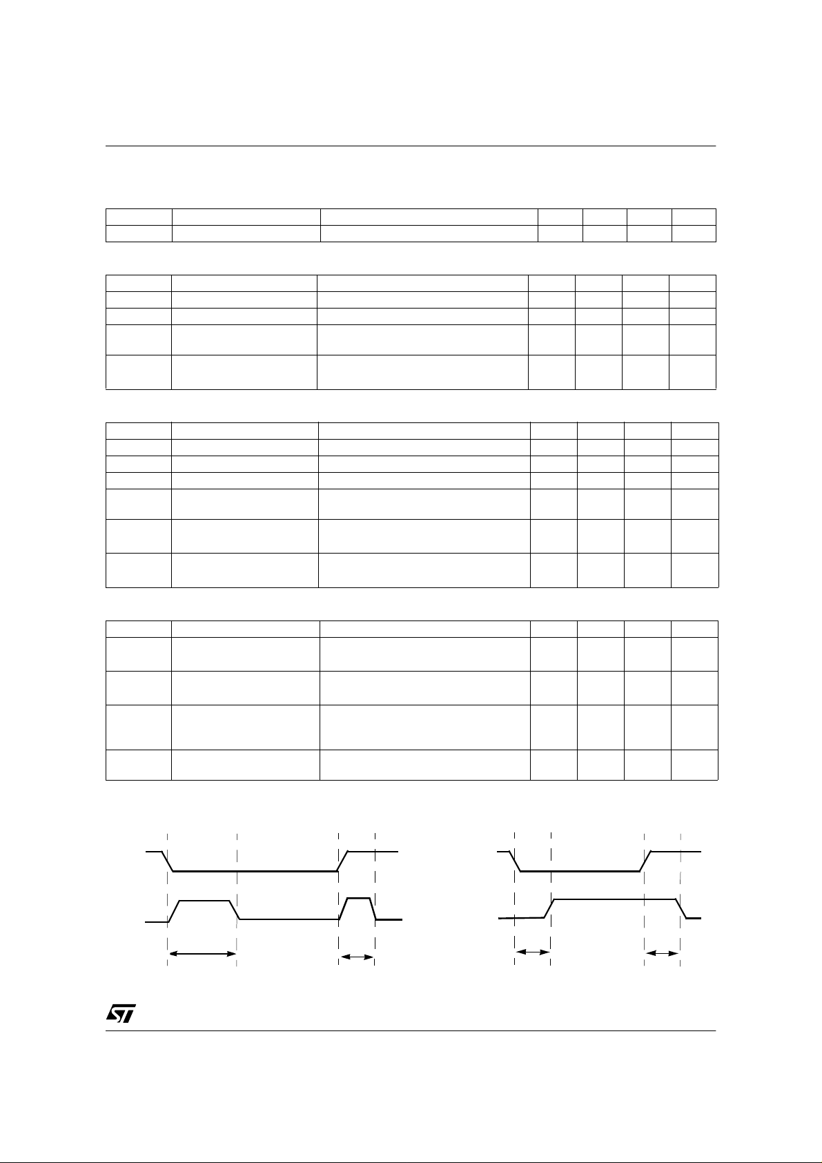
Switching time Waveforms
V
OUTn
dV
/dt
OUT
(on)
V
INn
td
(on)
80%
10%
90%
dV
/dt
OUT
(off)
t
td
(off)
t
TRUTH TABLE
CONDITIONS INPUT OUTPUT STATUS
Normal Operation
Current Limitation
Overtemperature
Undervoltage
Overvoltage
Output Voltage > V
Output Current < I
OL
OL
L
H
L
H
H
L
H
L
H
L
H
L
H
L
H
L
H
L
X
X
(T
(T
< T
j
> T
j
L
L
L
L
L
L
H
H
L
H
TSD
TSD
H
H
H
) H
) L
H
L
X
X
H
H
L
H
H
L
6/20
 Loading...