

SGS Thomson Microelectronics VNQ600 Datasheet
®
VNQ600
QUAD CHAN NEL HIGH SIDE SOLID STATE RELAY
TYPE R
DS(on)
(*) I
lim
V
CC
VNQ600 35mΩ 25A 36 V
(*) Per each channel
■ DC SHORT CIRCUIT CURRENT: 25A
■ CMOS COMPATIBLE INPUTS
■ PROPORTIONAL LOAD CURRENT SENSE
■ UNDERVOLTAGE & OVERVOLTAGE
SHUT-DOWN
n
■ OVERVOLTAGE CLAMP
■ THERMAL SHUT-DOWN
■ CURRENT LIMITATION
■ VERY LOW STAND-BY POWER DISSIPATION
■ PROTECTION AGAINST:
LOSS OF GROUND & LOSS OF VCC
n
■ REVERSE BATTERY PROTECTION (**)
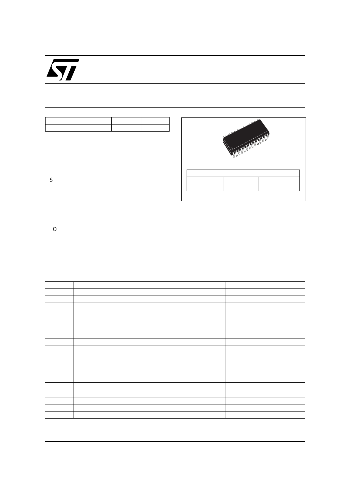
SO-28 VNQ600 VNQ60013TR
package. The VND600 is a monolithic device
designed in| STMicroelectronics VIPower M0-3
Technology. The VNQ600 is intended for dri ving
any type of multiple loads with one side connected
to ground. This device has four independent
channels and four analog sense outputs which
SO-28 (DOUBLE ISLAND)
ORDER CODES
PACKAGE TUBE T&R
deliver currents proportional to the outputs
currents. Active current limitation combined with
DESCRIPTION
The VNQ600 is a quad HSD formed by
assembling two VND600 chips in the same SO-28
thermal shut-down and automatic restart protect
the device against overload . Device auto mati call y
turns off in case of ground pin disconnection.
ABSOLUTE MAXIMUM RATING
Symbol Parameter Value Unit
V
-V
I
OUT
I
I
V
CSENSE
I
GND
V
ESD
E
MAX
P
T
T
Supply voltage ( continuous) 41 V
CC
Reverse supply voltage (continuous) -0.3 V
CC
Output current ( continuo us), for each channel 15 A
Reverse output current (continu ous), for each channel -15 A
R
Input current +/- 10 mA
IN
Current sense maximum voltage
Ground current at T
< 25°C (continuous) -200 mA
pins
-3
+15
Electro static Discharge ( Human Body M odel: R=1.5KΩ; C=100pF)
- INPUT
- CURRENT SENSE
- OUTPUT
- V
CC
Maxim u m Sw itchin g En ergy
(L=0.11m H ; R
Power dissipation (per island) at T
tot
Junction operat ing temperature Internally Limited ° C
j
Storage temperature -55 to 150 °C
stg
=0Ω; V
L
=13.5V ; T
bat
=150ºC ; IL=40A)
jstart
=25°C 6.25 W
lead
4000
2000
5000
5000
126 mJ
V
V
V
V
V
V
(**) See app lication sch em atic at page 9.
June 20 03 1/18

VNQ600
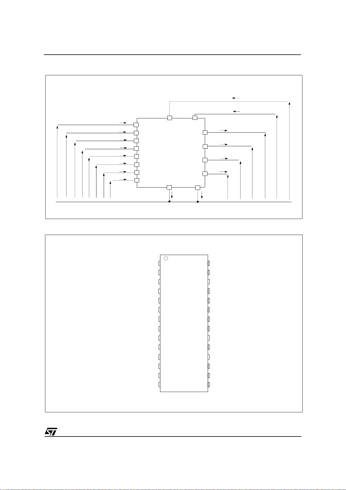
BLOCK DIAGRAM
OVERVOLTAGE
UNDERVOLT AGE
1,2
V
CC
INPUT 1
INPUT 2
GND 1,2
INPUT 3
INPUT 4
GND 3,4
OVERTEMP. 1
OVERTEMP. 2
OVERTEMP. 3
OVERTEMP. 4
LOGIC
LOGIC
DRIVER 1
I
OUT1
DRIVER 2
I
OUT2
OVERVOLT AGE
UNDERVOLTAGE
DRIVER 3
I
OUT3
DRIVER 4
I
OUT4
DEMA G 1
I
LIM1
K
DEMAG 2
I
LIM2
K
DEMAG 3
I
LIM3
K
DEMAG 4
I
LIM4
K
OUTPUT 1
CURRENT
SENSE 1
OUTPUT 2
CURRENT
SENSE 2
3,4
V
CC
OUTPUT 3
CURRENT
SENSE 3
OUTPUT 4
CURRENT
SENSE 4
2/18
CURRENT AND VOLTAGE CO NVENTIONS
I
VNQ600
S1,2
I
IN1
SENSE3
V
IN4
I
SENSE1
I
IN2
I
SENSE2
I
IN3
I
SENSE3
I
IN4
I
SENSE4
V
SENSE4
V
IN1
V
SENSE1
V
IN2
V
SENSE2
V
IN3
V
CONNECTION DIAGRAM ( TOP VIEW)
VCC1,2
GND 1,2
INPUT2
INPUT1
CURRENT
CURRENT SE NSE 2
V
CC
V
CC
GND 3,4
INPUT4
INPUT3
CURRENT SE NSE 3
CURRENT SE NSE 4
V
CC
SENSE 1
1,2
3,4
3,4
V
CC1,2
INPUT1
CUR. SENSE1
INPUT2
CUR. SENSE2
INPUT3
CUR. SENSE3
INPUT4
CUR. SENSE4
GND
1,2
1
14 15
OUTPUT1
OUTPUT2
OUTPUT3
OUTPUT4
I
GND1,2
V
CC3,4
GND
V
CC3,4
V
CC1,2
I
S3,4
I
OUT1
I
OUT2
I
OUT3
V
OUT3
I
OUT4
V
OUT4
3,4
I
GND3,4
28
V
1,2
CC
V
OUT2
V
OUT1
OUTPUT 2
OUTPUT 2
OUTPUT 2
OUTPUT 1
OUTPUT 1
OUTPUT 1
OUTPUT 4
OUTPUT 4
OUTPUT 4
OUTPUT 3
OUTPUT 3
OUTPUT 3
V
3,4
CC
3/18
VNQ600
THERMAL DATA (Per island)
Symbol Parameter Value Unit
R
thj-lead
R
thj-amb
R
thj-amb
(*) When mounted on a standard single-sided FR-4 board with 0.5cm2 of Cu (at leas t 35µ m thick) connected to all VCC pins.
Horizontal mounting and no artificial air flow.
ELECTRICAL CHARACTERISTICS (8V<VCC<36V; -40°C<Tj<150°C; unless otherwise specified)
(Per each channel)
POWER
Symbol Parameter Test Condi tions Min Typ Max Unit
V
CC
V
USD
V
OV
R
ON
V
clamp
I
(**) Supply current
S
I
L(off1)
I
L(off 2)
I
L(off3)
I
L(off4)
Thermal resistance Junction-lead 20 °C/W
Thermal resistance Juncti on-ambient (one chip ON) 60 (*) °C/W
Thermal Resistan ce Juncti on-ambient (two chips ON) 46 (*) °C/W
(**) Operating supply voltage 5.5 13 36 V
(**) Undervoltage shut-down 3 4 5.5 V
(**) Overvo ltage shut-down 36 V
On state res istance
1,2,3,4=5A; Tj=25°C
I
OUT
I
1,2,3,4=5A; Tj=150°C
OUT
I
1,2,3,4=3A; V
OUT
CC
=6V
35
70
120
Clamp Volt age ICC=20mA (see note 1) 41 48 55 V
Off Stat e; V
Off Stat e; V
T
=25°C
j
On State; V
=0A; R
I
OUT
Off state output current VIN=V
OUT
Off State Output Current VIN=0V; V
Off State Output Current VIN=V
Off State Output Current VIN=V
OUT
OUT
=13V; VIN=V
CC
=13V; VIN=V
CC
OUT
OUT
=0V
=0V;
12
12
=13V; VIN=5V;
CC
=3.9KΩ
SENSE
=0V 0 50 µA
=3.5V -75 0 µA
OUT
=0V; Vcc=13V; Tj =125°C 5 µA
=0V; Vcc=13V; Tj =25°C 3 µA
40
25
6
mΩ
mΩ
mΩ
µA
µA
mA
SWITCHING (VCC=13V)
Symbol Parameter Test Conditions Min Typ Max Unit
t
d(on)
t
d(off)
Turn-on del a y time RL=2.6Ω channels 1,2,3,4 (see fig. 1) 40 µs
Turn-off delay time RL=2.6Ω channels 1,2,3,4 (see fig. 1) 40 µs
See
/dt)onTurn-on voltage slope RL=2.6Ω channels 1,2,3,4 (see fig. 1)
(dV
OUT
relative
diagram
See
(dV
OUT
/dt)
Turn-off voltage s lope RL=2.6Ω channels 1,2,3,4 (see fig. 1)
off
relative
diagram
PROTECTIONS
Symbol Parameter Test Conditions Min Typ Max Unit
V
I
lim
T
TSD
T
R
T
hyst
V
demag
V
ON
(**) Per island
4/18
=13V
DC Short circuit current
CC
5.5V<V
CC
<36V
Thermal shut-down
temper ature
Thermal reset temperatu re 135 °C
Thermal hysteresis 7 15 °C
Turn-off output voltage clamp I
Output voltage drop limitation I
=2A; L= 6m H VCC-41 VCC-48 VCC-55 V
OUT
=0.5A; Tj= -40°C.. .+150°C 50 mV
OUT
25 40 70
70
150 175 200 °C
V/µs
V/µs
A
A
1
VNQ600
CURRENT SENSE (9V< V
< 16V) (See Fig. 3)
CC
Symbol Parameter Test Conditions Min Typ Max Unit
I
K
dK
1/K1
K
dK2/K
K
dK3/K
V
SENSE1,2
V
SENSEH
1
2
3
I
OUT/ISENSE
Current Sense Ratio Drift
I
OUT/ISENSE
Current Sense Ratio Drift
2
I
OUT/ISENSE
Current Sense Ratio Drift
3
Max analog sense output
voltage
Analog sense output voltage in
overtemperature condition
Analog Sense Output
R
VSENSEH
t
DSENSE
Impeda nce in
Overtem peratur e Condition
Current sense delay response to 90% I
=0.35A ; V
OUT1,2
T
= -40°C. .. +150°C
j
I
or I
OUT1
V
SENSE
open; Tj= -40°C...150° C
I
=2A; V
OUT
T
= 25°C...+150°C
j
or I
I
OUT1
other channels open;
T
=-40°C...150°C
j
I
=4A; V
OUT
T
= 25°C...+150°C
j
or I
I
OUT1
other channels open;
T
=-40°C...150°C
j
=5.5V; I
V
CC
R
SENSE
V
>8V; I
CC
R
SENSE
VCC=13V; R
=0.5A;
OUT2
=0.5V; other channels
SENSE
=5A; V
OUT2
SENSE
=15A; V
OUT2
OUT1,2
=10KΩ
OUT1,2
=10KΩ
SENSE
VCC=13V; Tj>T
open
(see note 2) 500 µs
SENSE
=0.5V;
SENSE
3300 43 50 6000
-10 +10 %
=2.5V; Tj=-40°C
=4V;
SENSE
3900
4150
4850
4850
6000
5800
-6 +6 %
=4V; Tj=-40°C
SENSE
=4V;
4150
4400
4900
4900
6000
5750
-6 +6 %
=2A;
=4A;
2
4
=3.9K Ω 5V
; All channels
TSD
400 Ω
V
V
LOGIC INPUT
Symbol Parameter Test Conditions Min Typ Max Unit
V
IL
V
IH
V
I(hyst)
I
IL
I
IN
V
ICL
Note 1: V
clamp
Note 2: current sense signal delay after pos itive input sl ope.
Note: Sense pin doesn’t have to be left float ing.
Low level input voltage 1.25 V
High level input voltage 3.25 V
Input hysteres is voltag e 0.5 V
Input current VIN=1.5V 1 µA
Input current VIN=3.5V 10 µA
=1mA
I
Input clamp voltage
and VOV are correlated. Typical difference is 5V.
IN
I
= -1mA
IN
66.8
-0.7
8V
V
5/18
2
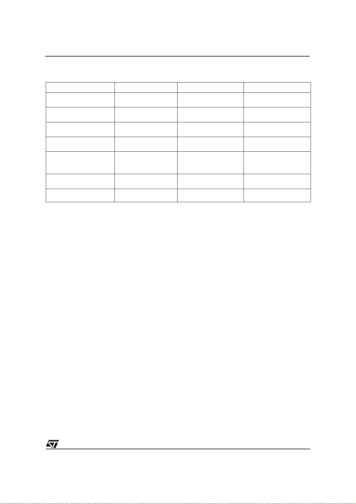
TRUTH TABLE (per channel)
CONDITIONS INPUT OUTPUT SENSE
Normal op eration
Overtemperature
Undervoltage
Overvoltage
Short circuit to GND
Short circuit to V
Negative output voltage
clamp
CC
VNQ600
L
H
L
H
L
H
L
H
L
H
H
L
H
LL 0
L
H
L
L
L
L
L
L
L
L
L
(T
j<TTSD
(T
j>TTSD
H
H
0
Nominal
0
V
SENSEH
0
0
0
0
0
) 0
) V
SENSEH
0
< Nomin a l
6/18
 Loading...