

SGS Thomson Microelectronics VNQ05XSP1613TR, VNQ05XSP16 Datasheet
®
VNQ05XSP16
QUAD CHAN NEL HIGH SIDE SOLID STATE RELAY
TYPE RON(*) I
OUT
V
CC
VNQ05XSP16 110mΩ 5A (*) 36 V
(*) Per each channel
■ OUTPUT CURRENT (CONTINUOUS): 5A
■ CMOS COMPATIBLE INPUTS
■ MULTIPLEXED PROPORTIONAL LOAD
CURRENT SENSE
■ UNDERVOLTAGE & OVERVOLTAGE
PowerSO-16
ORDER CODES
PACKAGE TUBE T&R
PowerSO-16™ VNQ05XSP16 VNQ05XSP1613TR
TM
SHUT- DOWN
■ OVERVOLTAGE CLAMP
■ THERMAL SHUT DOWN
■ CURRENT LIMITATION
■ VERY LOW STAND-BY POWER DISSIPATION
■ PROTECTION AGAINST:
n LOSS OF GROUND & LOSS OF V
■ REVERSE BATTERY PROTECTION (**)
CC
DESCRIPTION
The VNQ05XSP16 is a monolithic device
designed in STMicroelectronics VIPower M0-3
Technology. It is intende d for driving any type of
multiple loads with one side connec ted to grou nd.
Active V
against low energy spikes (see ISO7637 transient
pin voltage clamp protects the devi ce
CC
compatibility table). This device has four
independent channels and one multiplexed analog
sense output which del iver a current propor tional
to the selected output current. SenseEnable pin
allows to connect any number of VNQ05XSP16 on
the same Current Sense line. Active current
limitation combined with thermal shut-down and
automatic restart protect the device against
overload. Device automatically turns off in case of
ground pin disconnection.
ABSOLUTE MAXIMUM RATING
Symbol Parameter Value Unit
V
-V
I
OUT
I
I
V
CSENSE
I
GND
V
ESD
P
E
MAX
T
T
STG
T
Supply voltage (continuous) 41 V
CC
Reverse supply voltage (continuous) -0.3 V
CC
Output current (continuous), for each channel Internally limited A
Rever se output c urrent (c ontinuous), for each channel -5 A
R
Input current (IN1,IN2,IN3,IN4,SELA,SELB,SENSENABLE) +/- 10 mA
IN
Current sense maximum voltage
Ground current at T
<25°C (continuous) -200 mA
case
Electros tatic Discharge (H um an Body Mo del: R=1.5Ω; C=100pF )
- INPUT
- CURRENT SENSE
- OUTPU T
- V
CC
Power dissipation at T
tot
=25°C 78 W
case
Maximum Switching Energy
(L=1.72mH; R
Junction operating temperature Internally limited °C
j
Case Operating Temperature - 40 to 150 °C
c
=0Ω; V
L
=13.5V; T
bat
=150ºC; IL=7.5A)
jstart
Storage temperature -55 to 150 °C
-3
+15
4000
2000
5000
5000
76 mJ
V
V
V
V
V
V
(**) See appl ic ation schem atic at page 9
March 2 003 1/17
VNQ05XSP16
BLOCK DIAGRAM
OVERVOLTAGE
UNDERVOLT AGE
V
CC
INPUT 1
INPUT 2
INPUT 3
INPUT 4
SELECT A
SELECT B
SENSE ENABL E
GND
CURRENT SENSE
OVERTEMP . 1
OVERTEMP. 2
OVERTEMP. 3
OVERTEMP. 4
ANALO G
LOGIC
DIAG
LOGIC
QUAD
Mux
DRIVER 1
DEMAG
Ot
1
CS
1
Same structure for the channels2,3,4
I
Vds
1
LIM 1
LIM 1
K
CS1
CS2
CS3
CS4
I
OUT1
OUTPUT 1
OUTPUT 2
OUTPUT 3
OUTPUT 4
2/17

CURRENT AND VOLTAGE CO NVENTIONS
I
IN1
I
V
SELB
V
IN2
I
IN3
I
IN4
I
SENSE
I
SELA
I
SELB
I
SENSENABLE
SENSENABLE
V
IN1
V
IN2
V
IN3
V
IN4
V
SENSE
V
SELA
INPUT1
INPUT2
INPUT3
INPUT4
V
CC
SENSE
SELA
SELB
SENSENABLE
GND
OUTPUT1
OUTPUT2
OUTPUT3
OUTPUT4
I
GND
I
S
I
OUT1
I
OUT2
I
OUT3
I
OUT4
V
OUT4
V
VNQ05XSP16
V
OUT2
OUT3
V
OUT1
V
CC
CONNECTION DIAGRAM ( TOP VIEW)
INPUT 1
INPUT 2
INPUT 3
INPUT 4
C.SENSE
SENSENABLE
SELA
SELB
V
CC
10
11
12
13
14
15
16
17
89
7
6
5
4
3
2
1
GROUND
N.C.
OUTPUT 1
OUTPUT 2
N.C.
OUTPUT 3
OUTPUT 4
V
CC
3/17
VNQ05XSP16
THERMAL DATA
Symbol Parameter Value Unit
R
thj-case
R
thj-amb
Thermal resistance jun ction-case (MAX) 1.6 °C/W
Thermal resistance jun ction-a m bient (MAX) 51.6 (*) °C/W
(*) When mounted on FR4 printed circuit board with 0.5 cm² of copper area (at least 35 µm thick) connected to all V
CC
pins
ELECTRICAL CHARACTERISTICS (8V<VCC<36V; -4 0°C<Tj<150°C; unless o therwise specified) (Per each channel)
POWER
Symbol Parameter Test Conditions Min Typ Max Unit
V
V
USD
V
R
V
clamp
I
I
L(off1)
I
L(off2)
I
L(off3)
I
L(off4)
SWITCHING ( V
Operating supply voltage 5.5 13 36 V
CC
Under voltage shut down 3 4 5.5 V
Overvoltage shut down 36 V
OV
1,2,3,4=1A; Tj=25°C
I
OUT
On state resistan ce
ON
I
1,2,3,4=1A; Tj=150°C
OUT
I
1,2,3,4=0.5A; VCC=6V
OUT
Clam p Vo ltage ICC=20mA (See note 1) 41 48 55 V
CC
=13V
OUT
=0A;
Supply current
S
Off State Output Current VIN=V
Off State Output Current VIN=0V; V
Off State Output Current VIN=V
Off State Output Current VIN=V
=13V)
CC
Off state; Inputs=n.c.; V
On state; V
R
SENSE
=5V; VCC=13V; I
IN
=3.9k Ω
=0V 0 50 µA
OUT
=3.5V -75 0 µA
OUT
=0V; Vcc=13V; Tj=125°C 5 µA
OUT
=0V; Vcc=13V; Tj=25°C 3 µA
OUT
110
220
330
80
10
mΩ
mΩ
mΩ
µA
mA
Symbol Parameter Test Conditions Min Typ Max Unit
Turn-on delay tim e RL=2.6Ω channels 1,2,3,4 (see figure 2) 40 µs
Turn-off delay time RL=2.6Ω channels 1,2,3,4 (see figure 2) 40 µs
/
OUT
Turn-on voltage s lope RL=2.6Ω channels 1,2,3,4 (see figure 2)
on
/
OUT
Turn-off voltage slope RL=2.6Ω channels 1,2,3,4 (see figure 2)
off
See
relative
diagram
See
relative
diagram
V/µs
V/µs
(dV
(dV
t
d(on)
t
d(off)
dt)
dt)
PROTECTIONS
Symbol Parameter Test Conditions Min Typ Max Unit
I
lim
T
TSD
T
T
HYST
V
demag
V
ON
Note 1: V
=13V
V
DC short circuit current
CC
5.5V<V
CC
<36V
Thermal shut down
temperature
Thermal reset
R
temperature
Ther m al hy steresis 715 °C
Turn-off output voltage
clamp
Output voltage dr op
limitation
and VOV are correlated. Typical difference is 5V.
clamp
I
=2A; L=6mH VCC-41 VCC-48 VCC-55 V
OUT
I
=0.1A
OUT
T
=-40°C...+150°C
j
57.51010A
150 175 200 °C
135 °C
50 mV
4/17
1
A
VNQ05XSP16
CURRENT SENSE (9V< VCC <16V)
Symbol Parameter Test Conditions Min Typ Max Unit
I
K
1
dK
1/K1
K
2
dK
2/K2
K
3
dK
3/K3
I
SENSEO
V
SENSE1,2,3,4
I
OUT/ISENSE
Current Sense Ratio
Drift
I
OUT/ISENSE
Current Sense Ratio
Drift
I
OUT/ISENSE
Current Sense Ratio
Drift
Analog Sense
Leakage Current
Max analog sense
output voltage
Analog sense output
V
SENSEH
voltage in
overtemperature
condition
Analog sense output
R
VSENSEH
impe da nc e i n
overt em p erature
condition
t
DSENSE
Current sense delay
=0.1A; V
OUT
T
=-40...+150°C
j
I
=0.1A; V
OUT
T
= -40°C...+150°C
j
I
=1.0A, V
OUT
T
=-40...+150°C
j
I
=1.0A; V
OUT
T
=-40°C...+150°C
j
I
=2.0A, V
OUT
T
=-40...+150°C
j
I
=2.0A; V
OUT
T
=-40°C...+150°C
j
VCC=6...16V;
I
=0A;V
OUT
T
=-40°C...+150°C
j
V
CC
R
SENSE
V
CC
R
SENSE
=5.5V, I
=10kΩ
>8V, I
=10kΩ
SENSE
OUT1,2,3,4
VCC=13V; R
=13V; Tj>T
V
CC
All Channels Open
V
=13V; R
CC
(see note 2)
=0.5V
SENSE
SENSE
SENSE
SENSE
SENSE
SENSE
=0V;
OUT1,2,3,4
=0.5V;
=4V
=4V;
=4V
=4V;
=1.0A
650 950 1200
-10 +10 %
800 1000 1200
-8 +8 %
850 1000 1150
-6 +6 %
010µA
2
=2.0A
4
= 3.9kΩ 5.5 V
SENSE
;
TSD
SENSE
=3.9kΩ
400 Ω
300 500 µs
V
V
LOGIC CHARACTERISTICS (Inputs, Sela&b, Sensenable)
Symbol Parameter Test Conditions Min Typ Max Unit
V
IL
V
IH
V
I(hyst)
I
IL
I
IN
V
ICL
Note 2: current sense signal delay after pos itive input sl ope.
Note: Sense pin doesn’t have to be left float ing.
Inpu t low level
voltage
Input high level
voltage
Input hysteres is
voltage
Low level input
current
High level inp u t
current
Input clamp voltage
=1.25V 1 µA
V
IN
VIN=3.25V 10 µA
I
=1mA
IN
I
=-1mA
IN
3.25 V
0.5 V
66.8
-0.7
1.25 V
8V
V
5/17
2
VNQ05XSP16
TRUTH TABLE
CONDITIONS INPUT OUTPUT SENSE
Normal op eration
Overtemperature
Undervoltage
Overvoltage
L
H
L
H
L
H
L
H
L
Short circuit to GND
H
H
Short circuit to V
CC
Negative output voltage
clamp
L
H
LL 0
TRUTH TABLE
SENSENABLE SELB SELA SENSE
L X X High Impedance
HL LI
HL HI
HH LI
HH HI
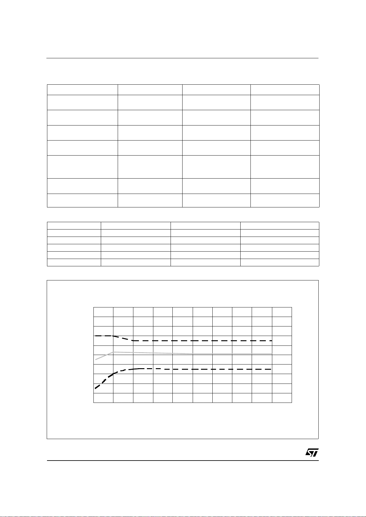
Figure 1: I
OUT/ISENSE
versus I
OUT
L
H
L
L
L
L
L
L
L
L
L
(T
(T
H
H
0
Nominal
0
V
SENSEH
0
0
0
0
0
) 0
j<TTSD
) V
j>TTSD
SENSEH
0
< Nomin a l
SENSE=IOUT1
SENSE=IOUT2
SENSE=IOUT3
SENSE=IOUT4
/K
/K
/K
/K
6/17
1
I
OUT/ISENSE
1500
1400
1300
1200
1100
1000
900
800
700
600
500
012345678910
I
(A )
OUT
max. T j= -4 0°C< < 150°C
typical value
min. T j= - 40 ° C< <150°
C
 Loading...