VNP10N06
”OMNIFET”:
FULLY AUTOPROTECTED POWER MOSFET
June 1997
1
2
3
TO-220
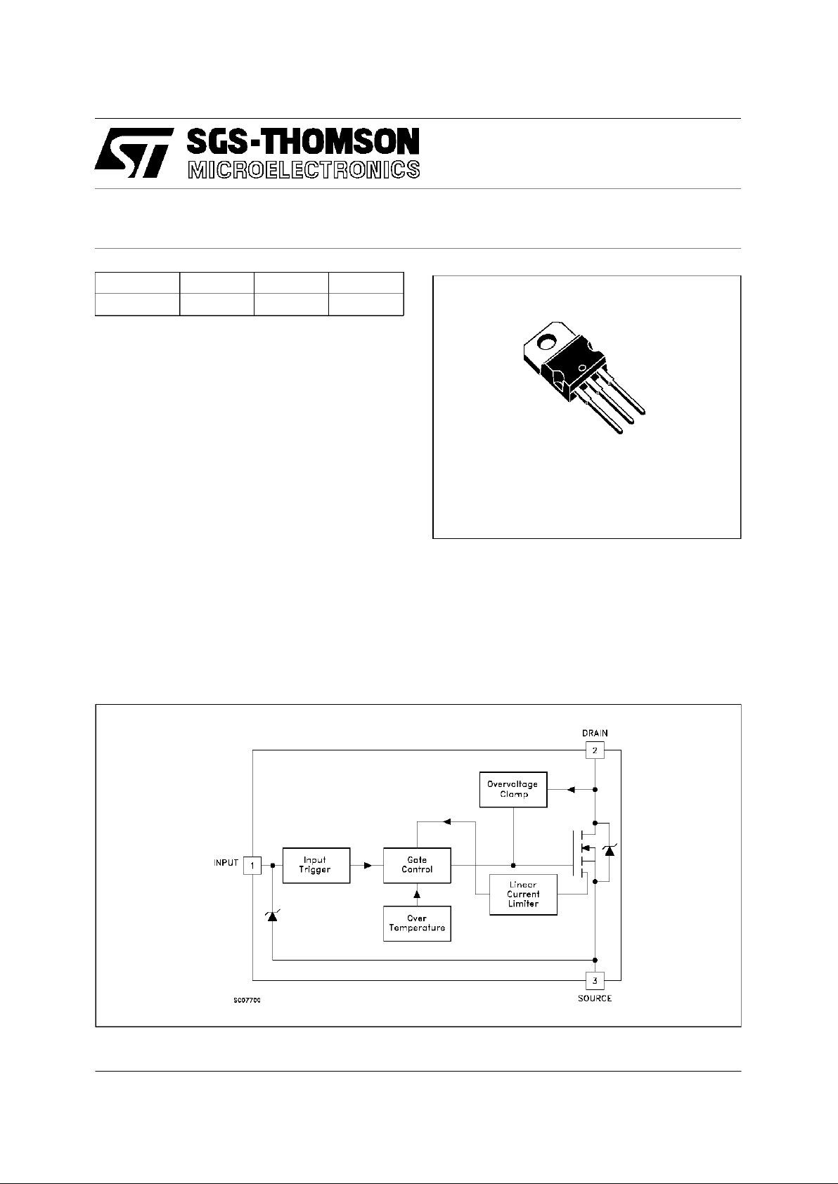
BLOCK DIAGRAM
TYPE V
clamp
R
DS(on)
I
lim
VNP10N06 60 V 0.3 Ω 10 A
■ LINEARCURRENTLIMITATION
■ THERMALSHUT DOWN
■ SHORTCIRCUIT PROTECTION
■ INTEGRATEDCLAMP
■ LOW CURRENTDRAWN FROM INPUT PIN
■ LOGICLEVEL INPUTTHRESHOLD
■ ESDPROTECTION
■ SCHMITTTRIGGER ON INPUT
■ HIGH NOISE IMMUNITY
■ STANDARD TO-220 PACKAGE
DESCRIPTION
The VNP10N06 is a monolithic device made
using SGS-THOMSON Vertical Intelligent Power
M0 Technology, intended for replacement of
standard power MOSFETS in DC to 50 KHz
applications. Built-in thermal shut-down, linear
current limitation and overvoltage clamp protect
the chip in harsh enviroments.
1/11

ABSOLUTEMAXIMUM RATING
Symbol Parameter Value Unit
V
DS
Drain-source Voltage (Vin= 0 ) Int er nall y Clamped V
V
in
Input Voltage Int er nall y Clamped V
I
in
Input Current ± 20 mA
I
D
Drain Current Internally Limited A
I
R
Reverse DC Output Current -15 A
V
esd
Elect r o st at ic Discharge (C= 100 pF, R=1. 5 KΩ)
4000 V
P
tot
Tot al Dissipat ion at Tc=25oC42W
T
j
Oper at i ng Junct ion Temperat ur e Internally Limited
o
C
T
c
Case Operating Temperature Internally Limited
o
C
T
stg
St orage Temperature -55 t o 150
o
C
THERMAL DATA
R
thj-case
R
thj-amb
Ther mal Resis t an ce Junction- case M ax
Ther mal Resis t an ce Junction- ambient Max
3
62.5
o
C/W
o
C/W
ELECTRICAL CHARACTERISTICS (T
case
=25oC unlessotherwise specified)
OFF
Symbol Parameter Test Condition s Min. Typ. Max. Unit
V
CLAMP
Drain-source Clamp
Volt age
ID= 200 mA Vin= 0 50 60 70 V
V
IL
Input Low Level
Volt age
I
D
= 100 µAVDS=16V
1.5 V
V
IH
Input High Lev el
Volt age
R
L
=27Ω VDD=16V
V
DS
=0.5V
3.2 V
V
INCL
Input-Source Reverse
Clamp Voltage
Iin=-1mA
I
in
=1mA
-1
8
-0.3
11
V
V
I
DSS
Zer o I npu t V olt age
Drain Current (V
in
=0)
V
DS
=50V Vin=V
IL
VDS<35V Vin=V
IL
250
100
µA
µA
I
ISS
Supply Current from
Input Pin
VDS=0V Vin= 5 V 150 300 µA
ON (∗)
Symbol Parameter Test Condition s Min. Typ. Max. Unit
R
DS(on)
St at ic Drain-sour ce On
Resistance
Vin=7V ID=1A TJ< 125oC0.150.3Ω
DYNAMIC
Symbol Parameter Test Condition s Min. Typ. Max. Unit
C
oss
Out put Capacit anc e VDS=13V f=1MHz Vin= 0 350 500 pF
VNP10N06
2/11

ELECTRICAL CHARACTERISTICS (continued)
SWITCHING(∗∗)
Symbol Parameter Test Condition s Min. Typ. Max. Unit
t
d(on)
t
r
t
d(off)
t
f
Turn-on Delay Time
Rise Time
Turn-off Delay T ime
Fall T ime
VDD=16V Id=1A
V
gen
=7V R
gen
=10Ω
(see figure 3)
1100
550
200
100
1600
900
400
200
ns
ns
ns
ns
t
d(on)
t
r
t
d(off)
t
f
Turn-on Delay Time
Rise Time
Turn-off Delay T ime
Fall T ime
VDD=16V Id=1A
V
gen
=7V R
gen
=1000Ω
(see figure 3)
1.2
1
1.6
1.2
1.8
1.5
2.3
1.8
µs
µs
µs
µs
(di/dt)
on
Tur n-on Current Slope VDD=16V ID=1A
V
in
=7V R
gen
=10Ω
1.5 A/µs
Q
i
Total Input Charge VDD=12V ID=1A Vin=7V 13 nC
SOURCE DRAIN DIODE
Symbol Parameter Test Condition s Min. Typ. Max. Unit
V
SD
(∗)ForwardOnVoltage ISD=1A Vin=V
IL
0.8 1.6 V
t
rr
(∗∗)
Q
rr
(∗∗)
I
RRM
(∗∗)
Reverse Re covery
Time
Reverse Re covery
Charge
Reverse Re covery
Current
I
SD
= 1 A di/dt = 100 A/µs
V
DD
=30V Tj=25oC
(see test cir cuit, figure 5)
125
0.22
3.5
ns
µC
A
PROTECTION
Symbol Parameter Test Condition s Min. Typ. Max. Unit
I
lim
Drain Current Limit Vin=7V VDS=13V 6 10 15 A
t
dlim
(∗∗) Step Response
Current Lim it
Vin=7V VDSstepfrom0to13V 12 20 µs
T
jsh
(∗∗) Ov ert emperatu re
Shut dow n
150
o
C
T
jrs
(∗∗) Ov ert emperatu re Reset 135
o
C
E
as
(∗∗) Si ngle Pulse
Avalanche E ner gy
starting Tj=25oCVDD=24V
V
in
=7V R
gen
=1KΩ L=10mH
250 m J
(∗) Pulsed: Pulse duration = 300 µs,duty cycle 1.5 %
(∗∗) Parameters guaranteed by design/characterization
VNP10N06
3/11

PROTECTION FEATURES
During Normal Operation, the INPUT pin is
electrically connected to the gate of the internal
power MOSFET through a low impedance path
as soon as V
IN>VIH
.
The device then behaves like a standard power
MOSFET and can be used as a switch from DC
to 50KHz. The only difference from the user’s
standpoint is that a small DC current (typically
150 µA) flows into the INPUT pin in order to
supplythe internalcircuitry.
During turn-off of an unclamped inductive load
the output voltage is clamped to a safe level by
an integrated Zener clamp between DRAIN pin
and the gateof theinternal Power MOSFET.
In this condition, the Power MOSFET gate is set
to a voltage high enough to sustain the inductive
load current even if the INPUT pin is driven to 0V.
The device integrates an active current limiter
circuit which limits the drain current I
D
to I
lim
whateverthe INPUTpin Voltage.
When the current limiter is active, the device
operatesin thelinear region,so power dissipation
may exceed the heatsinkingcapability. Both case
and junction temperatures increase, and if this
phase lasts long enough, junction temperature
may reach the overtemperaturethreshold T
jsh
.
If T
j
reaches T
jsh
, the device shuts down
whatever the INPUT pin voltage. The device will
restart automaticallywhen T
j
has cooled down to
T
jrs
VNP10N06
4/11
 Loading...