

VNH100N04
”OMNIFET”:
FULLY AUTOPROTECTED POWER MOSFET
TARGET DATA
September 1994
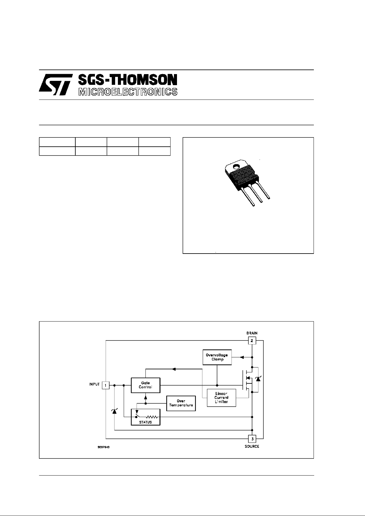
BLOCK DIAGRAM
TYPE V
clamp
R
DS(on)
I
lim
VNH100 N04 42 V 0.012 Ω 100 A
■ LINEAR CURRENT LIMITATION
■ THERMAL SHUT DOWN
■ SHORT CIRCUIT PROTECTION
■ INTEGRATED CLAMP
■ LOW CURRENT DRAWN FROM INPUT PIN
■ DIAGNOSTIC FEEDBACKTHROUGH INPUT
PIN
■ ESD PROTECTION
■ DIRECT ACCESS TO THE GATE OF THE
POWER MOSFET (ANALOG DRIVING)
■ COMPATIBLE WITH STANDARD POWER
MOSFET
■ STANDARD TO-218 PACKAGE
DESCRIPTION
The VNH100N04 is a monolithic device made
using SGS-THOMSON Vertical Intelligent Power
M0 Technology, intended for replacement of
standard power MOSFETS in DC to 50 KHz
applications. Buit-in thermal shut-down, linear
current limitation and overvoltage clamp protect
the chip in harsh enviroments.
Fault feedback can be detected by monitoring the
voltage at the input pin.
TO-218
1/7
ABSOLUTE MAXIMUM RATING
Symb o l Parameter Val u e Unit
V
DS
Drain - source Voltage (Vin= 0) Inte r nally Clamp ed V
V
in
Input Voltage 18 V
I
D
Drain C ur rent Inte r nally Limit ed A
I
R
Reverse DC O utput Current -50 A
V
esd
Electrost at ic D is c h ar ge (C= 100 p F , R=1. 5 KΩ ) 2000 V
P
tot
Total Dissipation at Tc=25oC208W
T
j
Oper at ing Junction Temperat ure Inte r nally Limit ed
o
C
T
c
Case Operating Temperature Internally Limited
o
C
T
stg
St orage Temperature -55 to 150
o
C
THERMAL DATA
R
thj-case
R
thj-amb
Thermal Resistance Junc tion-c as e Max
Thermal Resistance Junction- ambient Max
0.6
30
o
C/W
o
C/W
ELECTRICAL CHARACTERISTICS (T
case
=25oC unless otherwise specified)
OFF
Symbol Parameter Test Condi tions Min. Typ. Max. Unit
V
CLAMP
Drain - source Clamp
Volt age
ID=30A Vin= 0 36 42 48 V
V
CLTH
Drain - source Clamp
Thr e s hold Voltage
ID=2mA Vin=0 35 V
V
INCL
Input-Source Rev ers e
Clam p V oltage
Iin=-1mA -1 -0.3 V
I
DSS
Zero Input V oltage
Drain C ur rent (V
in
=0)
V
DS
=13V
V
DS
=25V
50
200
µA
µA
I
ISS
Supply Current f rom
Input Pin
VDS=0V Vin= 10 V 250 500 µ A
ON (∗)
Symbol Parameter Test Condi tions Min. Typ. Max. Unit
V
IS(th)
Input Threshold
Volt age
VDS=VinID=1mA 0.8 3 V
R
DS(on)
St at ic Dr ain- source On
Resistance
Vin=10V ID=30A
V
in
=5V ID=30A
0.012
0.015ΩΩ
DYNAMIC
Symbol Parameter Test Condi tions Min. Typ. Max. Unit
g
fs
(∗)Forward
Tr ansconduct anc e
VDS=13V ID=30A 40 S
C
oss
Out put Cap ac itance VDS=13V f=1MHz Vin= 0 1800 3000 pF
VNH100N04
2/7

ELECTRICAL CHARACTERISTICS (continued)
SWITCHING
Symbol Parameter Test Condi tions Min. Typ. Max. Unit
t
d(on)
t
r
t
d(off)
t
f
Turn-on Delay Time
Rise Time
Tur n - of f Delay Time
Fall Time
VDD=15V Id=30A
V
gen
=10V R
gen
=10Ω
(see figure 3)
100
400
900
400
TBD
TBD
TBD
TBD
ns
ns
ns
ns
t
d(on)
t
r
t
d(off)
t
f
Turn-on Delay Time
Rise Time
Tur n - of f Delay Time
Fall Time
VDD=15V Id=30A
V
gen
=10V R
gen
=10Ω
T
j
=125oC
(see figure 3)
TBD
TBD
TBD
TBD
ns
ns
ns
ns
t
d(on)
t
r
t
d(off)
t
f
Turn-on Delay Time
Rise Time
Tur n - of f Delay Time
Fall Time
VDD=15V Id=30A
V
gen
=10V R
gen
=1000Ω
(see figure 3)
TBD
TBD
TBD
TBD
µs
µs
µs
µs
(di/dt)
on
Turn-on Current S lope VDD=15V ID=30A
Vin=10V
TBD A/µs
Q
g
Total Gate Charge VDD=12V ID=30A Vin=10V TBD nC
SOURCE DRAIN DIODE
Symbol Parameter Test Condi tions Min. Typ. Max. Unit
V
SD
(∗) Forward O n Voltage ISD=30A Vin=0 TBD V
t
rr
Q
rr
I
RRM
Reverse Recover y
Time
Reverse Recover y
Charge
Reverse Recover y
Current
ISD= 30 A di/dt = 100 A/µs
VDD=V Tj= 150oC
(see test circuit, figure 5)
TBD
TBD
TBD
ns
µC
A
PROTECTION
Symbol Parameter Test Condi tions Min. Typ. Max. Unit
I
lim
Drain C ur rent Limit Vin=10V VDS= 13 V 70 100 140 A
t
dlim
St ep Response
Current Limit
Vin=10V VDS=13V TBD µs
T
jsh
Overtemperature
Shut down
150 170 190
o
C
T
jrs
Ove rtempe rature Rese t 135
o
C
I
gf
Fault Sink Cu r rent Vin=10V VDS=13V 50 mA
E
as
Single Pulse
Avalanc he Ener gy
starting Tj=25oCVDD=20V
Vin=10V R
gen
=1KΩ L= mH
TBD J
(∗) Puls ed: Pulse dur ation = 300 µs, duty cycle 1.5 %
VNH100N04
3/7
 Loading...