VB927
HIGH VOLTAGE IGNITION COIL DRIVER
■ NO EXTERNALCOMPONENT REQUIRED
■ INTEGRATEDHIGH VOLTAGECLAMP
■ COILCURRENT LIMITINTERNALLYSET
■ HIGH RUGGEDNESS
DESCRIPTION
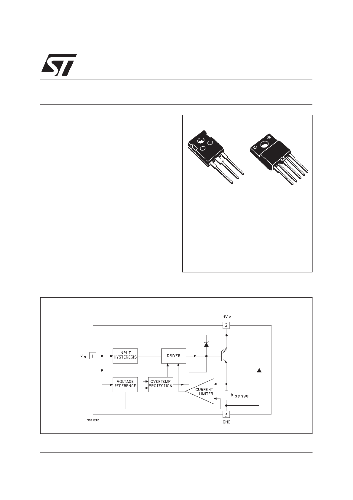
The VB927 is a monolithichigh voltage integrated
circuit made using STM VIPower Technology,
which combines a vertical current flow power
trilinton with a coil current limiting circuit and a
collectorvoltage clamping.
The device is peculiarly suitable for application in
high performance electronic car ignition, where
coil current limitation and voltage clamping are
required.
VB927FI
POWER IC
3
2
1
TO-247 ISOWATT5
BLOCK DIAGRAM
June 1998
1/5

VB927
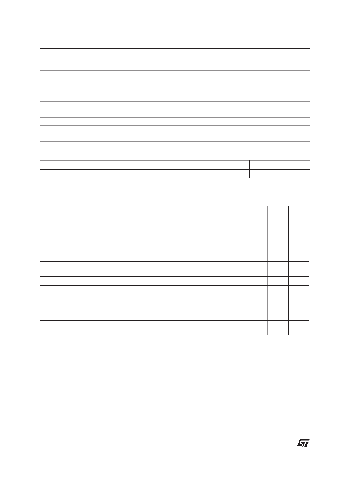
ABSOLUTEMAXIMUM RATING
Symbol Parameter Value Unit
VB927 VB927FI
HV
V
P
T
THERMAL DATA
R
thj-case
R
thj-amb
Collector Voltage Internally Limited V
c
Maximum Input Voltage 15 V
in
Collector Current Internally Limited A
I
c
Input Cur ren t Internally Limited mA
I
in
Tot al Diss ipation at Tc=25oC 150 70 W
tot
St orage Tem per atur e -40 t o150
stg
Oper at i ng Junction Temper at ure -40 to150
T
j
TO-247 ISOWATT5 Unit
Ther mal R es istance J unction-cas e Max 0.6 2
Ther mal Resis t an ce Junction- ambient Max 30
o
o
o
C
o
C
C/W
C/W
ELECTRICAL CHARACTERISTICS (V
=14 V, -40 < Tj<125oC unlessotherwise specified)
batt
Symbol Parameter Test Conditions Min. Typ. Max. Un it
I
leak
Collector Cut-off
Vin=0 HVc=250V 250 µA
Current
* Clamping Voltage -40 < Tj< 125oC 380 420 490 V
V
cl
V
cg(sat)
I
cl
I
V
f
V
in(h)
V
in(l)
V
n(hyst)
t
d(off)
T
Power S tage
Saturation Voltage
Ic=5A Iin= 10mA 25 ≤ Tj≤ 125oC
=6A Iin= 10mA -40 ≤ Tj≤ 25oC
I
c
* Coil Current Limit Vin=5V -40≤Tj≤125oC8.5 9.5A
Input Cur ren t Vin=5V Ic=5A
in
=5V Ic=5A Tj=25oC3
V
in
** Diode For ward V oltage If=10A Tj=25oC1.22.23.2V
Input Volt a ge (O N) On state input threshold 3.2 3.6 V
Input Volt a ge (O F F) Of f state input thr eshold 3 3.4 V
Input Voltage (Hyst.) 0.2 0.6 V
Turn-off Time Ic = 5 A 30 µs
Junction Temper at ur e
j
See n ot e1 150
2.5
3
10
10
V
V
mA
mA
o
C
Limit
* Coil data:primary resistance Rc= 0.4 - 0.8 Ω, primary inductance Lc=6-8mH
** Pulsed: Pulse duration = 300µs, duty cycle 1.5 %
Note1 : T
temperature, thethermal protection circuit will begin its action reducing the I
a functionof the R
min = 150oC means that the behaviour of the devicewill not be affected for junction temperature lower then 150oC . For higher
j
of the whole systemin which the device with be operating.
th
limit according with the power dissipation. Chip temperature is
cl
2/5

TO-247 MECHANICAL DATA
VB927
DIM.
MIN. TYP. MAX. MIN. TYP. MAX.
A 4.7 5.3 0.185 0.209
D 2.2 2.6 0.087 0.102
E 0.4 0.8 0.016 0.031
F 1 1.4 0.039 0.055
F3 2 2.4 0.079 0.094
F4 3 3.4 0.118 0.134
G 10.9 0.429
H 15.3 15.9 0.602 0.626
L 19.7 20.3 0.776 0.779
L3 14.2 14.8 0.559 0.413 0.582
L4 34.6 1.362
L5 5.5 0.217
M 2 3 0.079 0.118
Dia 3.55 3.65 0.140 0.144
mm inch
P025P
3/5

VB927
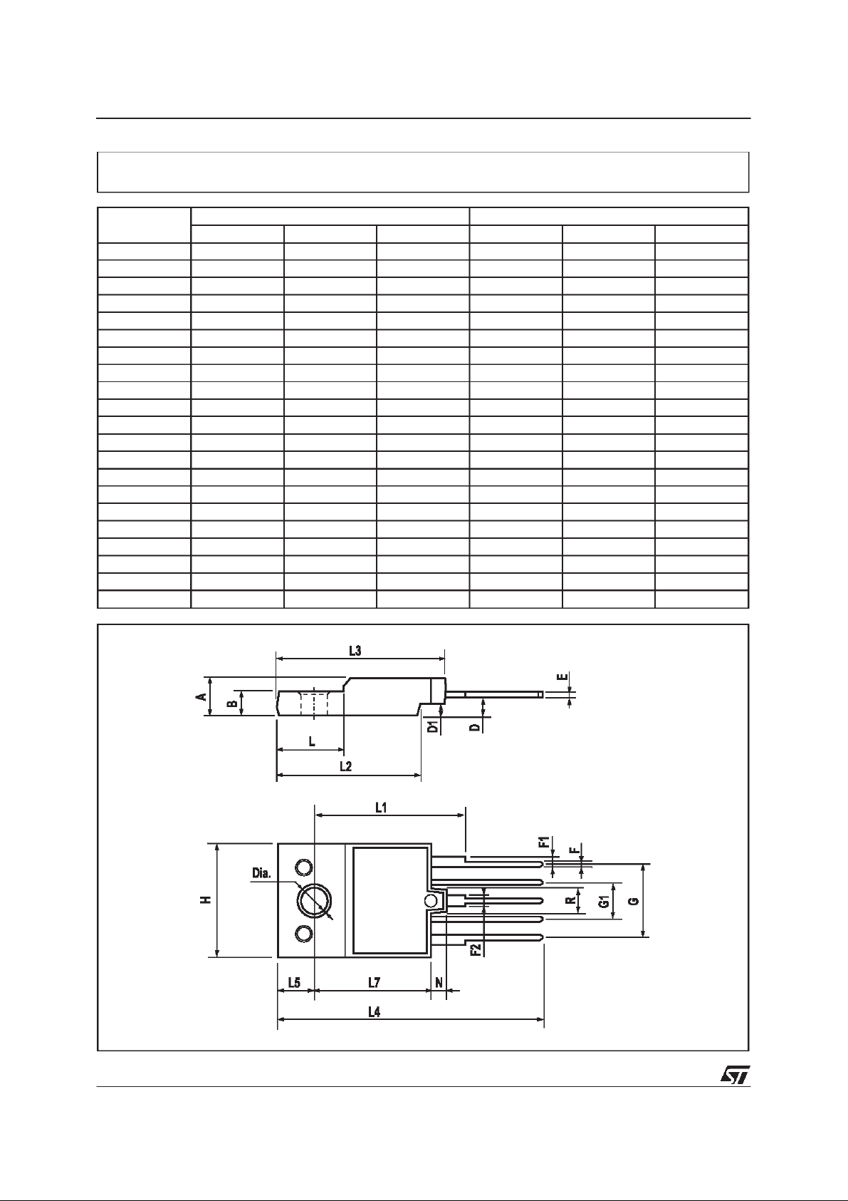
ISOWATT5MECHANICAL DATA
DIM.
A 5.35 5.65 0.210 0.222
B 3.3 3.8 0.130 0.149
D 2.95 3.1 0.116 0.122
D1 1.88 2.08 0.074 0.081
E 0.45 1 0.017 0.039
F 0.75 1 0.029 0.039
F1 1.5 0.059
F2 1.3 0.051
G 10.16 0.400
G1 5.08 0.200
H 15.8 16.2 0.622 0.637
L 9 0.354
L1 20.25 20.75 0.797 0.817
L2 19.10 19.9 0.751 0.783
L3 22.8 23.6 0.897 0.929
L4 34.9 36.9 1.374 1.452
L5 4.85 5.25 0.190 0.206
L7 16 0.630
N 2.1 2.3 0.082 0.090
R 3.1 0.122
MIN. TYP. MAX. MIN. TYP. MAX.
3.5 3.7 0.138 0.145
mm inch
4/5

VB927
Information furnished is believed to be accurateand reliable. However,STMicroelectronicsassumes no responsibility for the consequences
of use of such information nor for any infringement of patents or other rights of third parties which may result from its use. No license is
granted by implication orotherwise under any patent or patentrights of STMicroelectronics. Specification mentioned in this publication are
subject tochange without notice. This publicationsupersedes andreplaces all information previously supplied.STMicroelectronics products
are not authorized for use as critical componentsin life support devices or systems without express written approvalof STMicroelectronics.
Australia - Brazil - Canada - China - France- Germany- Italy - Japan - Korea - Malaysia - Malta - Mexico - Morocco- The Netherlands -
Singapore- Spain - Sweden- Switzerland- Taiwan- Thailand - United Kingdom- U.S.A.
The ST logo isa trademarkof STMicroelectronics
1998 STMicroelectronics–Printed in Italy – All Rights Reserved
STMicroelectronicsGROUP OF COMPANIES
.
5/5
 Loading...